Embed Size (px)
Citation preview
18EI504 Hall Ticket Number:
III/IV B.Tech (Regular) DEGREE EXAMINATION
February, 2021 Electronics and Instrumentation Engineering Fifth Semester Microcontrollers Time: Three Hours Maximum: 50 Marks Part – A Answer Question No.1 compulsorily. (1X10 = 10 Marks) 1. Answer all questions a) What is the ROM size of 8051 microcontroller? b) What is Machine Cycle? c) Mention the Math Flags present in Program Status Word. d) Upon reset which address is pointed by Stack Pointer? e) Write the instruction used for swapping upper and lower nibbles of accumulator. f) Which register is used for Timers mode selection? g) Which port is used for the generation of handshake lines in mode 1 or mode 2 of 8255 h) How many port lines in 8051 are needed for interfacing 4 x 4 key board? i) Mention the ports available in 16F8XX PIC. j) What is the number of instructions in 16F877 PIC? Answer ANY FOUR questions. (4X10=40 Marks) 2. a) Draw the pin diagram of 8051 microcontroller and explain the function of each pin briefly. 5M b) Explain Program Status Word (PSW) register of 8051 Microcontroller. 5M 3. a) Write about Stack of 8051 microcontroller. 5M b) Write about Interrupts of 8051 microcontroller. 5M 4. a) Explain various Arithmetic instructions of 8051 microcontroller. 5M b) Explain various Directives of 8051 microcontroller with examples. 5M 5. a) Write about TCON and TMOD resisters used in programming Timers. 5M b) Write assembly language program for arranging numbers in ascending order. 5M 6. a) Draw the block diagram of 8255 and explain each block briefly. 5M b) Draw the interfacing diagram of 4X4 keypad to 8051 and explain sequence of operations. 5M 7. a) Explain interfacing of ADC0808 with 8051. 5M b) Explain interfacing of Uni-Polar Stepper Motor with 8051. 5M 8. a) Explain briefly about various ports of PIC 16F877. 5M b) Explain STATUS and OPTION_REG registers. 5M 9. a) Draw the pin diagram of PIC 16F877. 5M b) Explain briefly about Program Memory and Data Memory of PIC 16F877. 5M
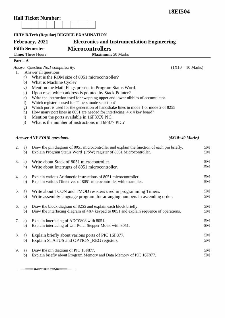
1. a) 4kB b) A machine cycle consists of the steps that a computer's processor executes whenever it receives a machine language. c) There are 4 math flags in PSW. They are Carry (C), Auxiliary Carry (AC), Overflow (OV) and Parity (P) flags. d) 07H e) SWAP f) TMOD g) Port C h)8 i) A,B,C,D and E j) 35 2.a)
Pins 1 to 8 − These pins are known as Port 1. This port doesn’t serve any other functions. It is internally pulled up, bi-directional I/O port.
Pin 9 − It is a RESET pin, which is used to reset the microcontroller to its initial values.
Pins 10 to 17 − These pins are known as Port 3. This port serves some functions like interrupts, timer input, control signals, serial communication signals RxD and TxD, etc.
Pins 18 & 19 − These pins are used for interfacing an external crystal to get the system clock.
Pin 20 − This pin provides the power supply to the circuit.
Pins 21 to 28 − These pins are known as Port 2. It serves as I/O port. Higher order address bus signals are also multiplexed using this port.
Pin 29 − This is PSEN pin which stands for Program Store Enable. It is used to read a signal from the external program memory.
Pin 30 − This is EA pin which stands for External Access input. It is used to enable/disable the external memory interfacing.
Pin 31 − This is ALE pin which stands for Address Latch Enable. It is used to demultiplex the address-data signal of port.
Pins 32 to 39 − These pins are known as Port 0. It serves as I/O port. Lower order address and data bus signals are multiplexed using this port.
Pin 40 − This pin is used to provide power supply to the circuit.
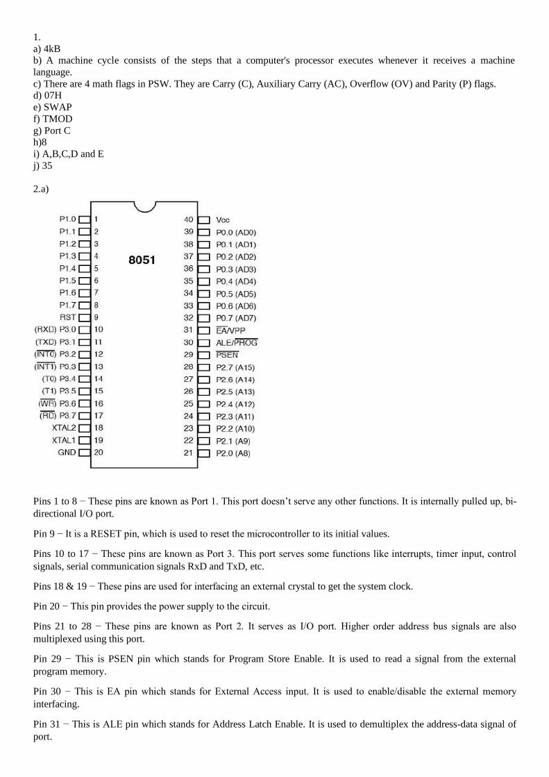
2.b)
3.a)
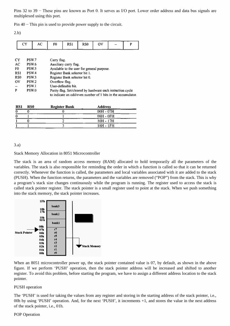
Stack Memory Allocation in 8051 Microcontroller
The stack is an area of random access memory (RAM) allocated to hold temporarily all the parameters of the variables. The stack is also responsible for reminding the order in which a function is called so that it can be returned correctly. Whenever the function is called, the parameters and local variables associated with it are added to the stack (PUSH). When the function returns, the parameters and the variables are removed (“POP”) from the stack. This is why a program’s stack size changes continuously while the program is running. The register used to access the stack is called stack pointer register. The stack pointer is a small register used to point at the stack. When we push something into the stack memory, the stack pointer increases.
When an 8051 microcontroller power up, the stack pointer contained value is 07, by default, as shown in the above figure. If we perform ‘PUSH’ operation, then the stack pointer address will be increased and shifted to another register. To avoid this problem, before starting the program, we have to assign a different address location to the stack pointer.
PUSH operation
The ‘PUSH’ is used for taking the values from any register and storing in the starting address of the stack pointer, i.e., 00h by using ‘PUSH’ operation. And, for the next ‘PUSH’, it increments +1, and stores the value in the next address of the stack pointer, i.e., 01h.
POP Operation
It is used for placing the values from the stack pointer’s maximum address to any other register’s address. If we use this ‘POP’ again, then it decrements by 1, and the value stored in any register is given as ‘POP’.
3.b)
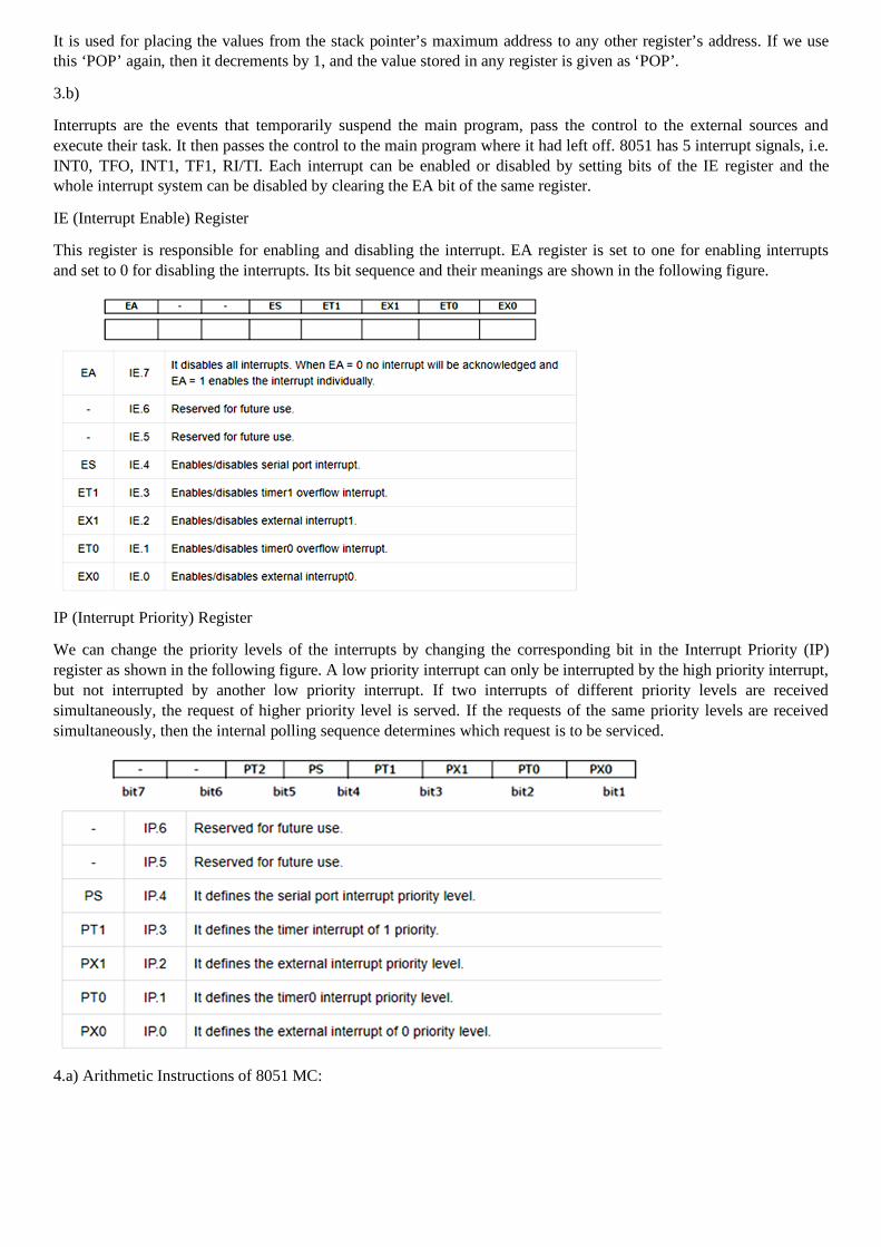
Interrupts are the events that temporarily suspend the main program, pass the control to the external sources and execute their task. It then passes the control to the main program where it had left off. 8051 has 5 interrupt signals, i.e. INT0, TFO, INT1, TF1, RI/TI. Each interrupt can be enabled or disabled by setting bits of the IE register and the whole interrupt system can be disabled by clearing the EA bit of the same register.
IE (Interrupt Enable) Register
This register is responsible for enabling and disabling the interrupt. EA register is set to one for enabling interrupts and set to 0 for disabling the interrupts. Its bit sequence and their meanings are shown in the following figure.
IP (Interrupt Priority) Register
We can change the priority levels of the interrupts by changing the corresponding bit in the Interrupt Priority (IP) register as shown in the following figure. A low priority interrupt can only be interrupted by the high priority interrupt, but not interrupted by another low priority interrupt. If two interrupts of different priority levels are received simultaneously, the request of higher priority level is served. If the requests of the same priority levels are received simultaneously, then the internal polling sequence determines which request is to be serviced.
4.a) Arithmetic Instructions of 8051 MC:
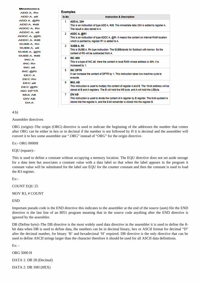
4.b)
Assembler directives
ORG (origin):-The origin (ORG) directive is used to indicate the beginning of the addresses the number that comes after ORG can be either in hex or in decimal if the number is not followed by H it is decimal and the assembler will convert it to hex some assembler use “.ORG” instead of “ORG” for the origin directive.
Ex:- ORG 0000H
EQU (equate):-
This is used to define a constant without accupying a memory location. The EQU directive does not set aside storage for a data item but associates a constant value with a data label so that when the label appears in the program it constant value will be substituted for the label use EQU for the counter constant and then the constant is used to load the R3 register.
Ex:-
COUNT EQU 25
MOV R3, # COUNT
END
Important pseudo code is the END directive this indicates to the assembler at the end of the source (asm) file the END directive is the last line of an 8051 program meaning that in the source code anything after the END directive is ignored by the assembler.
DB (Define byte):-The DB directive is the most widely used data directive in the assembler it is used to define the 8-bit data when DB is used to define data, the numbers can be in decimal binary, hex or ASCII format for decimal “D” after the decimal number, for binary ‘B’ and hexadecimal ‘H’ required. DB directive is the only directive that can be used to define ASCII strings larger than the character therefore it should be used for all ASCII data definitions.
Ex: -
ORG 5000 H
DATA 1: DB 28 (Decimal)
DATA 2: DB 39H (HEX)
DATA 3: 0101001 B (Binary)
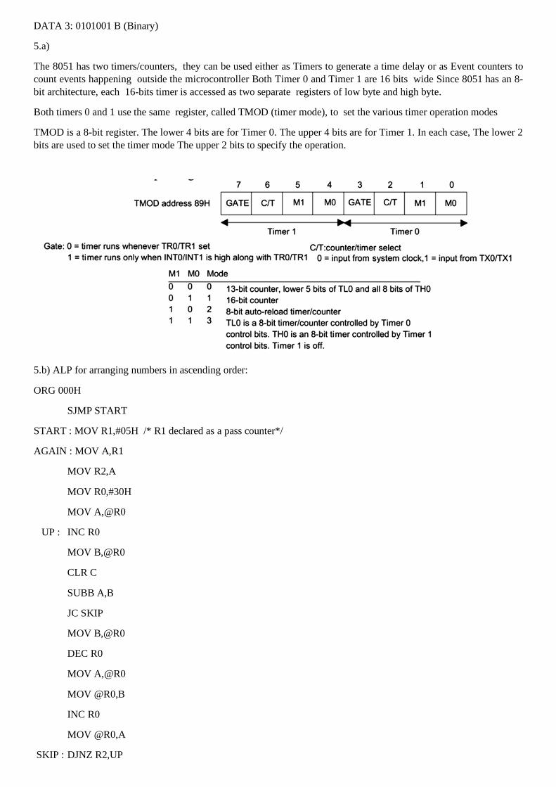
5.a)
The 8051 has two timers/counters, they can be used either as Timers to generate a time delay or as Event counters to count events happening outside the microcontroller Both Timer 0 and Timer 1 are 16 bits wide Since 8051 has an 8-bit architecture, each 16-bits timer is accessed as two separate registers of low byte and high byte.
Both timers 0 and 1 use the same register, called TMOD (timer mode), to set the various timer operation modes
TMOD is a 8-bit register. The lower 4 bits are for Timer 0. The upper 4 bits are for Timer 1. In each case, The lower 2 bits are used to set the timer mode The upper 2 bits to specify the operation.
5.b) ALP for arranging numbers in ascending order:
ORG 000H
SJMP START
START : MOV R1,#05H /* R1 declared as a pass counter*/
AGAIN : MOV A,R1
MOV R2,A
MOV R0,#30H
MOV A,@R0
UP : INC R0
MOV B,@R0
CLR C
SUBB A,B
JC SKIP
MOV B,@R0
DEC R0
MOV A,@R0
MOV @R0,B
INC R0
MOV @R0,A
SKIP : DJNZ R2,UP
DJNZ R1,AGAIN
STOP : SJMP STOP
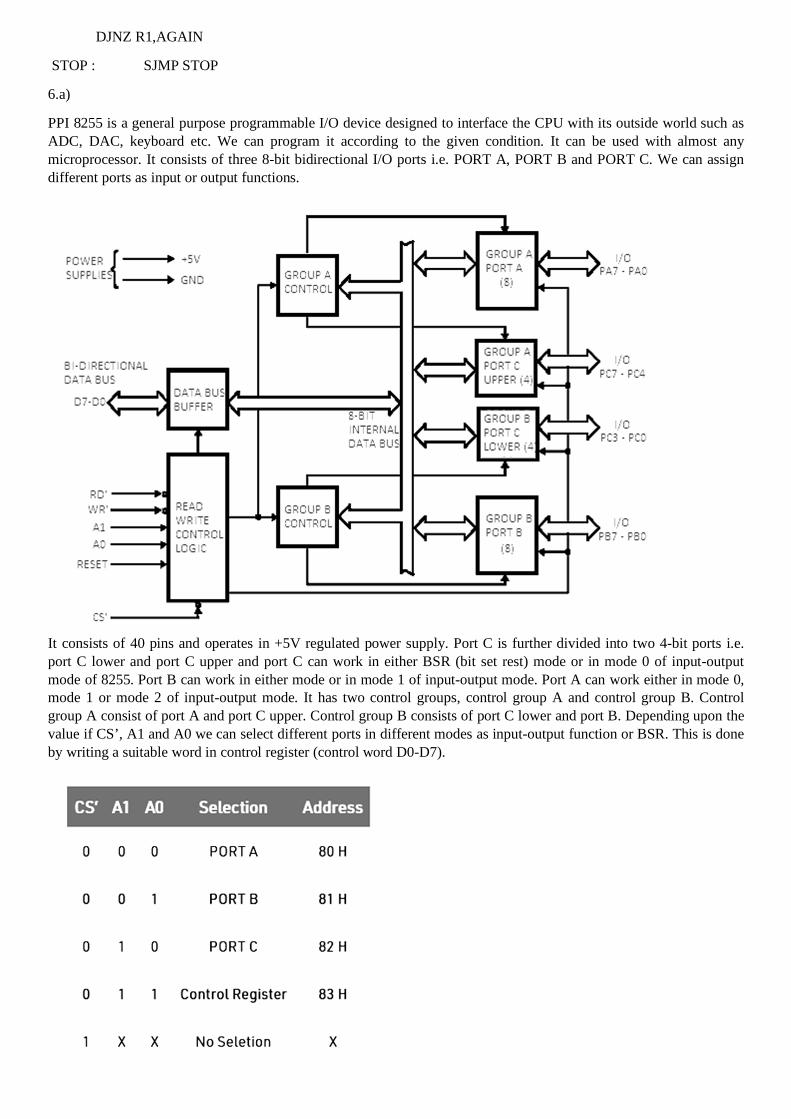
6.a)
PPI 8255 is a general purpose programmable I/O device designed to interface the CPU with its outside world such as ADC, DAC, keyboard etc. We can program it according to the given condition. It can be used with almost any microprocessor. It consists of three 8-bit bidirectional I/O ports i.e. PORT A, PORT B and PORT C. We can assign different ports as input or output functions.
It consists of 40 pins and operates in +5V regulated power supply. Port C is further divided into two 4-bit ports i.e. port C lower and port C upper and port C can work in either BSR (bit set rest) mode or in mode 0 of input-output mode of 8255. Port B can work in either mode or in mode 1 of input-output mode. Port A can work either in mode 0, mode 1 or mode 2 of input-output mode. It has two control groups, control group A and control group B. Control group A consist of port A and port C upper. Control group B consists of port C lower and port B. Depending upon the value if CS’, A1 and A0 we can select different ports in different modes as input-output function or BSR. This is done by writing a suitable word in control register (control word D0-D7).
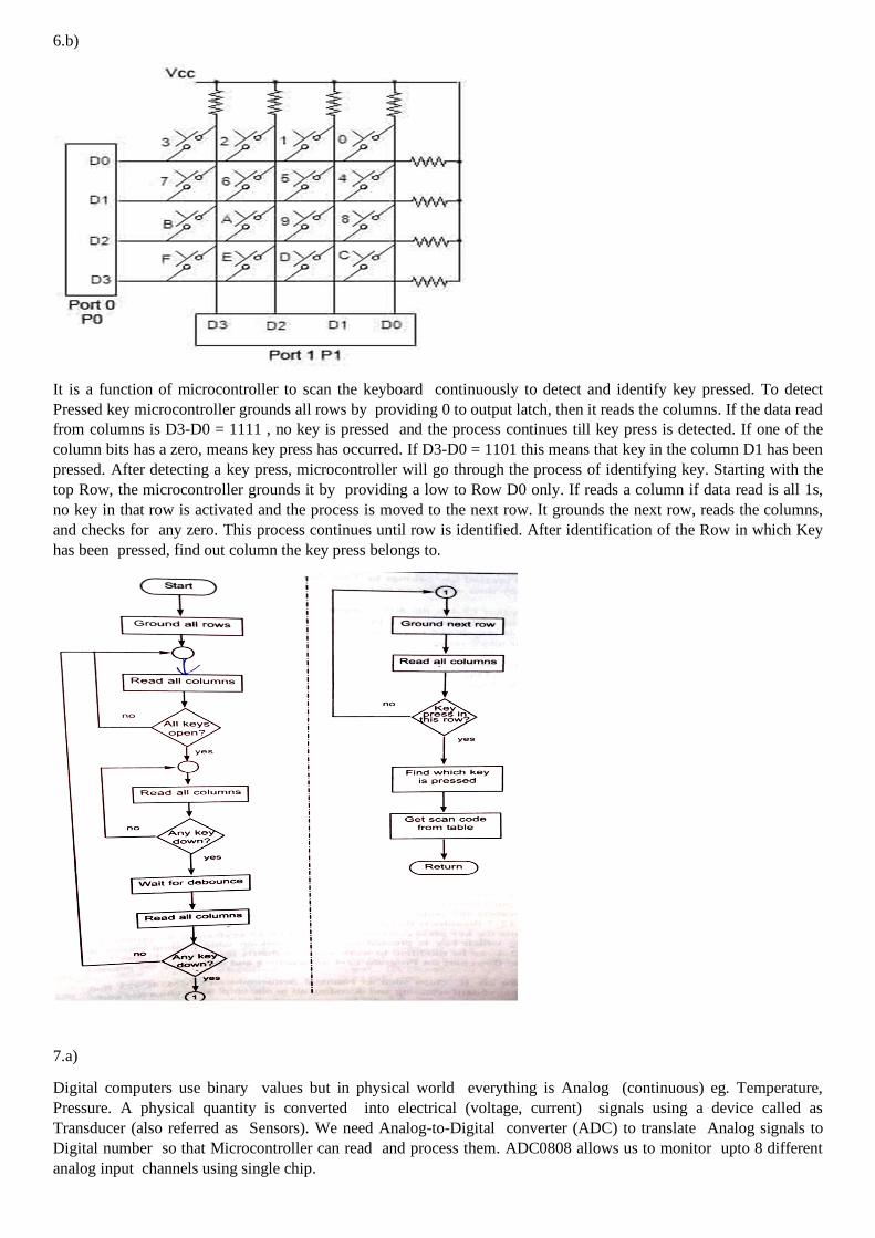
6.b)
It is a function of microcontroller to scan the keyboard continuously to detect and identify key pressed. To detect Pressed key microcontroller grounds all rows by providing 0 to output latch, then it reads the columns. If the data read from columns is D3-D0 = 1111 , no key is pressed and the process continues till key press is detected. If one of the column bits has a zero, means key press has occurred. If D3-D0 = 1101 this means that key in the column D1 has been pressed. After detecting a key press, microcontroller will go through the process of identifying key. Starting with the top Row, the microcontroller grounds it by providing a low to Row D0 only. If reads a column if data read is all 1s, no key in that row is activated and the process is moved to the next row. It grounds the next row, reads the columns, and checks for any zero. This process continues until row is identified. After identification of the Row in which Key has been pressed, find out column the key press belongs to.
7.a)
Digital computers use binary values but in physical world everything is Analog (continuous) eg. Temperature, Pressure. A physical quantity is converted into electrical (voltage, current) signals using a device called as Transducer (also referred as Sensors). We need Analog-to-Digital converter (ADC) to translate Analog signals to Digital number so that Microcontroller can read and process them. ADC0808 allows us to monitor upto 8 different analog input channels using single chip.
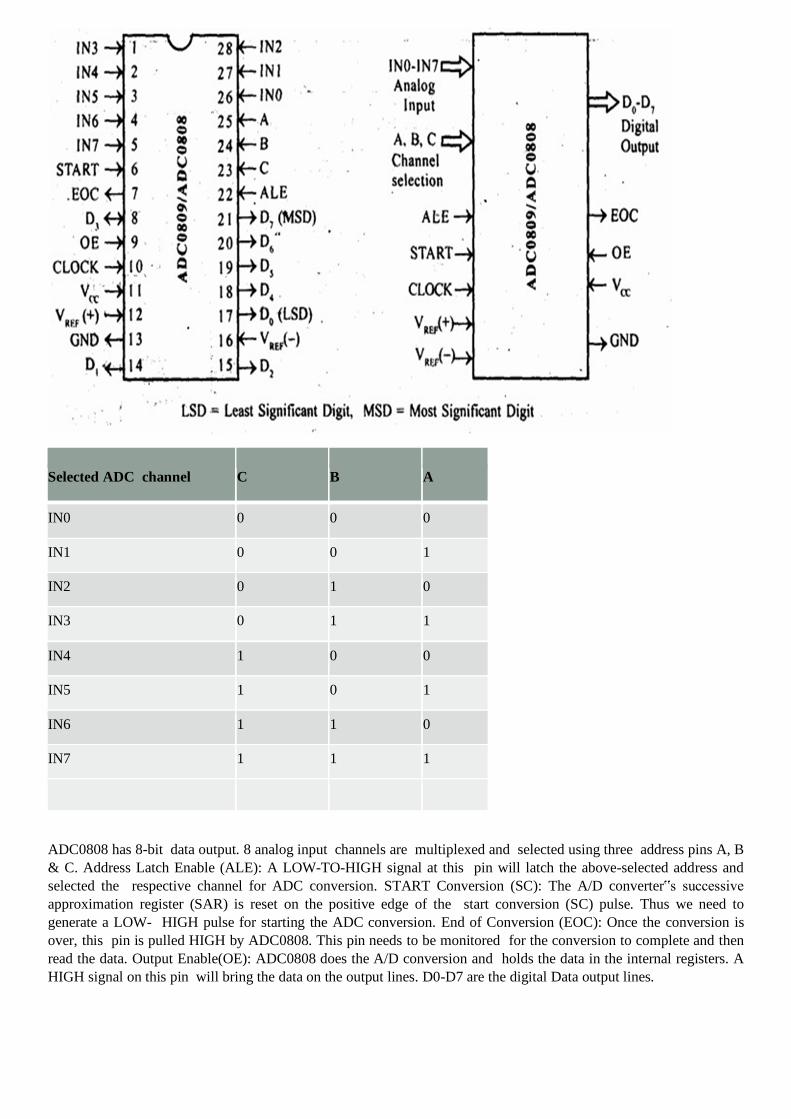
Selected ADC channel C B A
IN0 0 0 0
IN1 0 0 1
IN2 0 1 0
IN3 0 1 1
IN4 1 0 0
IN5 1 0 1
IN6 1 1 0
IN7 1 1 1
ADC0808 has 8-bit data output. 8 analog input channels are multiplexed and selected using three address pins A, B & C. Address Latch Enable (ALE): A LOW-TO-HIGH signal at this pin will latch the above-selected address and selected the respective channel for ADC conversion. START Conversion (SC): The A/D converter‟s successive approximation register (SAR) is reset on the positive edge of the start conversion (SC) pulse. Thus we need to generate a LOW- HIGH pulse for starting the ADC conversion. End of Conversion (EOC): Once the conversion is over, this pin is pulled HIGH by ADC0808. This pin needs to be monitored for the conversion to complete and then read the data. Output Enable(OE): ADC0808 does the A/D conversion and holds the data in the internal registers. A HIGH signal on this pin will bring the data on the output lines. D0-D7 are the digital Data output lines.
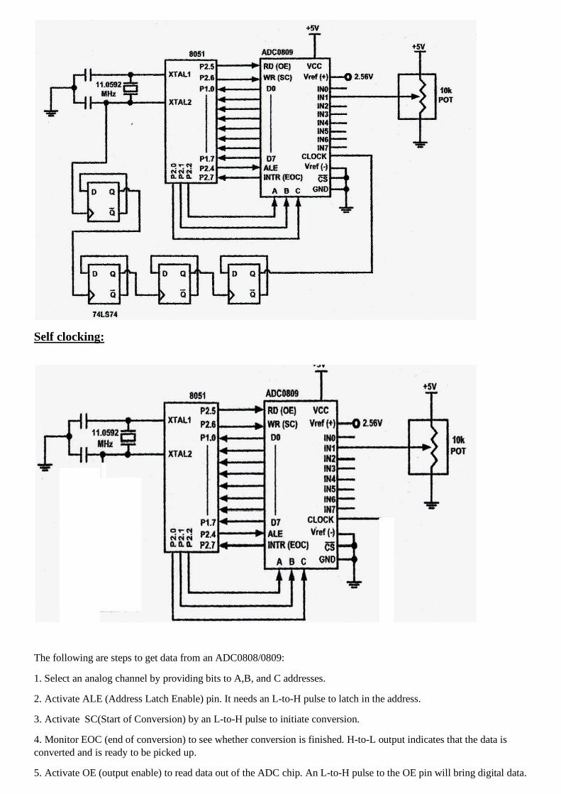
Self clocking:
The following are steps to get data from an ADC0808/0809:
1. Select an analog channel by providing bits to A,B, and C addresses.
2. Activate ALE (Address Latch Enable) pin. It needs an L-to-H pulse to latch in the address.
3. Activate SC(Start of Conversion) by an L-to-H pulse to initiate conversion.
4. Monitor EOC (end of conversion) to see whether conversion is finished. H-to-L output indicates that the data is converted and is ready to be picked up.
5. Activate OE (output enable) to read data out of the ADC chip. An L-to-H pulse to the OE pin will bring digital data.
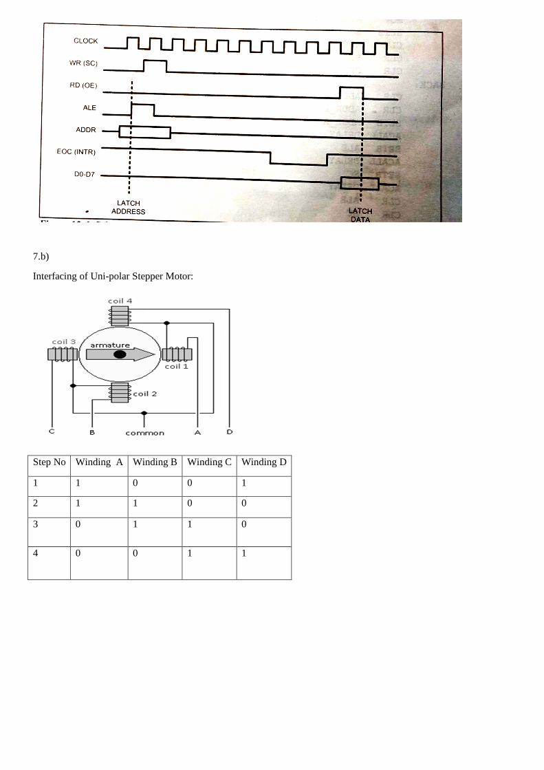
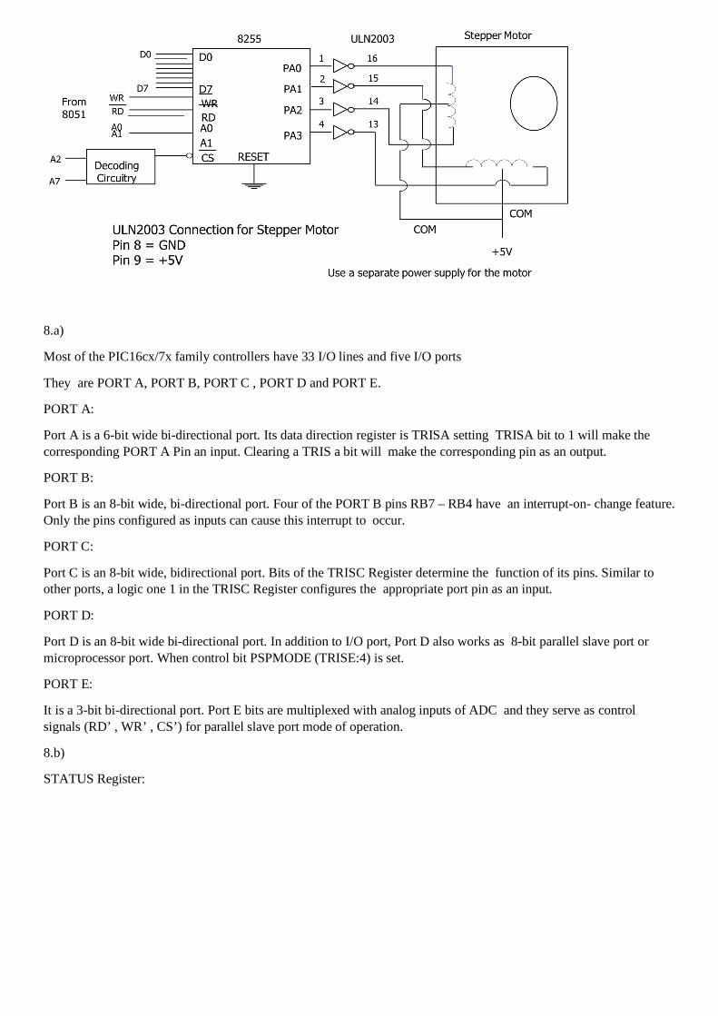
7.b)
Interfacing of Uni-polar Stepper Motor:
Step No Winding A Winding B Winding C Winding D
1 1 0 0 1
2 1 1 0 0
3 0 1 1 0
4 0 0 1 1
8.a)
Most of the PIC16cx/7x family controllers have 33 I/O lines and five I/O ports
They are PORT A, PORT B, PORT C , PORT D and PORT E.
PORT A:
Port A is a 6-bit wide bi-directional port. Its data direction register is TRISA setting TRISA bit to 1 will make the corresponding PORT A Pin an input. Clearing a TRIS a bit will make the corresponding pin as an output.
PORT B:
Port B is an 8-bit wide, bi-directional port. Four of the PORT B pins RB7 – RB4 have an interrupt-on- change feature. Only the pins configured as inputs can cause this interrupt to occur.
PORT C:
Port C is an 8-bit wide, bidirectional port. Bits of the TRISC Register determine the function of its pins. Similar to other ports, a logic one 1 in the TRISC Register configures the appropriate port pin as an input.
PORT D:
Port D is an 8-bit wide bi-directional port. In addition to I/O port, Port D also works as 8-bit parallel slave port or microprocessor port. When control bit PSPMODE (TRISE:4) is set.
PORT E:
It is a 3-bit bi-directional port. Port E bits are multiplexed with analog inputs of ADC and they serve as control signals (RD’ , WR’ , CS’) for parallel slave port mode of operation.
8.b)
STATUS Register:
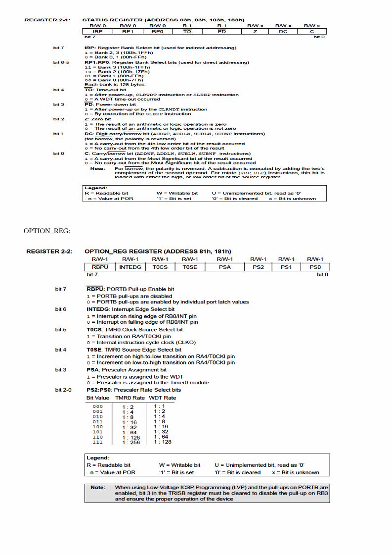
OPTION_REG:
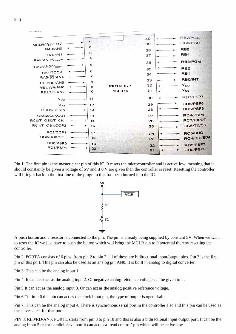
9.a)
Pin 1: The first pin is the master clear pin of this IC. It resets the microcontroller and is active low, meaning that it should constantly be given a voltage of 5V and if 0 V are given then the controller is reset. Resetting the controller will bring it back to the first line of the program that has been burned into the IC.
A push button and a resistor is connected to the pin. The pin is already being supplied by constant 5V. When we want to reset the IC we just have to push the button which will bring the MCLR pin to 0 potential thereby resetting the controller.
Pin 2: PORTA consists of 6 pins, from pin 2 to pin 7, all of these are bidirectional input/output pins. Pin 2 is the first pin of this port. This pin can also be used as an analog pin AN0. It is built in analog to digital converter.
Pin 3: This can be the analog input 1.
Pin 4: It can also act as the analog input2. Or negative analog reference voltage can be given to it.
Pin 5:It can act as the analog input 3. Or can act as the analog positive reference voltage.
Pin 6:To timer0 this pin can act as the clock input pin, the type of output is open drain.
Pin 7: This can be the analog input 4. There is synchronous serial port in the controller also and this pin can be used as the slave select for that port.
PIN 8: RE0/RD/AN5: PORTE starts from pin 8 to pin 10 and this is also a bidirectional input output port. It can be the analog input 5 or for parallel slave port it can act as a ‘read control’ pin which will be active low.
PIN 9: RE1/WR/AN6: It can be the analog input 6. And for the parallel slave port it can act as the ‘write control’ which will be active low.
PIN 10: RE2/CS/A7: It can be the analog input 7, or for the parallel slave port it can act as the ‘control select’ which will also be active low just like read and write control pins.
PIN 11 and 32: VDD: These two pins are the positive supply for the input/output and logic pins. Both of them should be connected to 5V.
PIN 12 and 31: VSS: These pins are the ground reference for input/output and logic pins. They should be connected to 0 potential.
PIN 13: OSC1/CLKIN: This is the oscillator input or the external clock input pin.
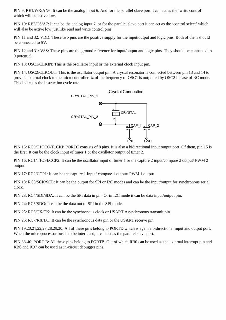
PIN 14: OSC2/CLKOUT: This is the oscillator output pin. A crystal resonator is connected between pin 13 and 14 to provide external clock to the microcontroller. ¼ of the frequency of OSC1 is outputted by OSC2 in case of RC mode. This indicates the instruction cycle rate.
PIN 15: RC0/T1OCO/T1CKI: PORTC consists of 8 pins. It is also a bidirectional input output port. Of them, pin 15 is the first. It can be the clock input of timer 1 or the oscillator output of timer 2.
PIN 16: RC1/T1OSI/CCP2: It can be the oscillator input of timer 1 or the capture 2 input/compare 2 output/ PWM 2 output.
PIN 17: RC2/CCP1: It can be the capture 1 input/ compare 1 output/ PWM 1 output.
PIN 18: RC3/SCK/SCL: It can be the output for SPI or I2C modes and can be the input/output for synchronous serial clock.
PIN 23: RC4/SDI/SDA: It can be the SPI data in pin. Or in I2C mode it can be data input/output pin.
PIN 24: RC5/SDO: It can be the data out of SPI in the SPI mode.
PIN 25: RC6/TX/CK: It can be the synchronous clock or USART Asynchronous transmit pin.
PIN 26: RC7/RX/DT: It can be the synchronous data pin or the USART receive pin.
PIN 19,20,21,22,27,28,29,30: All of these pins belong to PORTD which is again a bidirectional input and output port. When the microprocessor bus is to be interfaced, it can act as the parallel slave port.
PIN 33-40: PORT B: All these pins belong to PORTB. Out of which RB0 can be used as the external interrupt pin and RB6 and RB7 can be used as in-circuit debugger pins.


