Embed Size (px)
Citation preview
//INTEGRAS/ELS/PAGINATION/ELSEVIER UK/MAB/3B2/FINALS_03-11-03/CH001.3D – 1 – [1–27/27]28.11.2003 5:04PM
1Introduction to Microcontrollers
1.1 Introduction
A microcontroller is a computer with most of the necessary support chipsonboard. All computers have several things in common, namely:
. A central processing unit (CPU) that ‘executes’ programs.
. Some random-access memory (RAM) where it can store data that is variable.
. Some read onlymemory (ROM)where programs to be executed can be stored.
. Input and output (I/O) devices that enable communication to be establishedwith the outside world i.e. connection to devices such as keyboard, mouse,monitors and other peripherals.
There are a number of other common characteristics that define microcon-trollers. If a computer matches a majority of these characteristics, then it can beclassified as a ‘microcontroller’. Microcontrollers may be:
. ‘Embedded’ inside some other device (often a consumer product) so thatthey can control the features or actions of the product. Another name for amicrocontroller is therefore an ‘embedded controller’.
. Dedicated to one task and run one specific program. The program is storedin ROM and generally does not change.
. A low-power device. A battery-operated microcontroller might consume aslittle as 50 milliwatts.
A microcontroller may take an input from the device it is controlling andcontrols the device by sending signals to different components in the device.A microcontroller is often small and low cost. The components may be chosento minimise size and to be as inexpensive as possible.
The actual processor used to implement a microcontroller can vary widely. Inmany products, such as microwave ovens, the demand on the CPU is fairly low
//INTEGRAS/ELS/PAGINATION/ELSEVIER UK/MAB/3B2/FINALS_03-11-03/CH001.3D – 2 – [1–27/27]28.11.2003 5:04PM
and price is an important consideration. In these cases, manufacturers turn todedicated microcontroller chips – devices that were originally designed to below-cost, small, low-power, embedded CPUs. The Motorola 6811 and Intel8051 are both good examples of such chips.
A typical low-end microcontroller chip might have 1000 bytes of ROM and20 bytes of RAM on the chip, along with eight I/O pins. In large quantities, thecost of these chips can sometimes be just a few pence.
In this book the authors will introduce the reader to some of the Philips’ 8051family of microcontrollers, and show their working, with applications,throughout the book. The programming of these devices is the same and,depending on type of device chosen, functionality of each device is determinedby the hardware devices onboard the chosen device.
1.2 Microcontroller types
The predominant family of microcontrollers are 8-bit types since this wordsize has proved popular for the vast majority of tasks the devices have beenrequired to perform. The single byte word is regarded as sufficient for mostpurposes and has the advantage of easily interfacing with the variety of ICmemories and logic circuitry currently available. The serial ASCII data is alsobyte sized making data communications easily compatible with the microcon-troller devices. Because the type of application for the microcontroller may varyenormously most manufacturers provide a family of devices, each member ofthe family capable of fitting neatly into the manufacturer’s requirements. Thisavoids the use of a common device for all applications where some elements ofthe device would not be used; such a device would be complex and henceexpensive. The microcontroller family would have a common instruction subsetbut family members differ in the amount, and type, of memory, timer facility,port options, etc. possessed, thus producing cost-effective devices suitable forparticular manufacturing requirements. Memory expansion is possible with off-chip RAM and/or ROM; for some family members there is no on-chip ROM,or the ROM is either electrically programmable ROM (EPROM) or electricallyerasable PROM (EEPROM) known as flash EEPROM which allows for theprogram to be erased and rewritten many times. Additional on-chip facilitiescould include analogue-to-digital conversion (ADC), digital-to-analogue con-version (DAC) and analogue comparators. Some family members includeversions with lower pin count for more basic applications to minimise costs.Many microcontroller manufacturers are competing in the market place andrather than attempting to list all types the authors have restricted the text todevices manufactured by one maker. This does not preclude the book frombeing useful for applications involing other manufacturer’s devices; there is acommonality among devices from various sources, and descriptions within thetext can, in most cases, be applied generally. The chapters that follow will dealwith microcontroller family members available from Philips Semiconductors,and acknowledgement is due to the considerable assistance given by that
2 Introduction to microcontrollers
//INTEGRAS/ELS/PAGINATION/ELSEVIER UK/MAB/3B2/FINALS_03-11-03/CH001.3D – 3 – [1–27/27]28.11.2003 5:04PM
company in the production of this text. The Philips products are identified bythe numbering system:
8XCXXX
where in general, since there are exceptions, the digit following the 8 is:
0 for a ROMless device3 for a device with ROM7 for a device with EPROM/OTP (one time programmable)9 for a device with FEEPROM (flash).
Following the C there may be 2 or 3 digits. Additional digits, not shown above,would include such factors as clock speed, pin count, package code and tempera-ture range. Philips also produces a family of 16-bit microcontrollers in the eXtendedArchitecture (XA) range. For these devices Philips claims compatibility with the80C51 at source code level with full support for the internal registers, operatingmodes and 8051 instructions. Also claimed is a much higher speed of operationthan the 8051 devices. The XA products are identified by the numbering system:
PXAG3XXXX
where:
PXA is Philips 80C51 XAG3 is the derivative namenext digit is memory option:
0 ¼ ROM less
3 ¼ ROM
5 ¼ Bond-out ðemulationÞ7 ¼ EPROM=OTP
9 ¼ FEEPROM ðflashÞnext digit is speed:
J ¼ 25MHz
K ¼ 30MHZ
next digit is temperature:B ¼ 0�C toþ 70�C
F ¼ �40�C toþ 85�Cfinal digit is package code:
A ¼ Plastic Leaded Chip Carrier (PLCC)
B ¼ Quad Flat Pack (QFP)
etc.
The XA architecture supports:
. 16-bit fully static CPU with a 24-bit program and data address range;
. eight 16-bit CPU registers, each capable of performing all arithmetic andlogic operations as well as acting as memory pointers;
Microcontroller types 3
//INTEGRAS/ELS/PAGINATION/ELSEVIER UK/MAB/3B2/FINALS_03-11-03/CH001.3D – 4 – [1–27/27]28.11.2003 5:04PM
. both 8-bit and 16-bit CPU registers, each capable of performing all arith-metic and logic operations;
. an enhanced instruction set that includes bit-intensive logic operations andfast signed or unsigned 16� 16 multiplies and 32/16 divide;
. instruction set tailored for high-level language support;
. multitasking and real-time executives that include up to 32 vectored inter-rupts, 16 software traps, segmented data memory and banked registers tosupport context switching.
The next section of this chapter will look at a member of the Philips 80C51family in more detail.
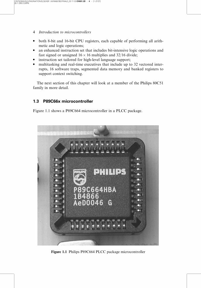
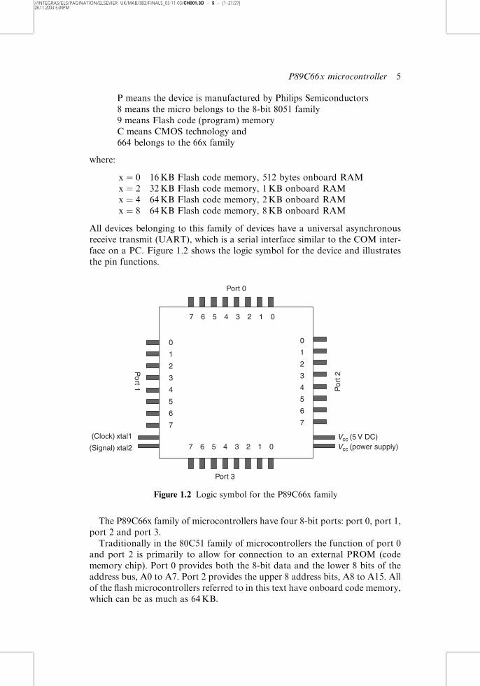
1.3 P89C66x microcontroller
Figure 1.1 shows a P89C664 microcontroller in a PLCC package.
Figure 1.1 Philips P89C664 PLCC package microcontroller
4 Introduction to microcontrollers
//INTEGRAS/ELS/PAGINATION/ELSEVIER UK/MAB/3B2/FINALS_03-11-03/CH001.3D – 5 – [1–27/27]28.11.2003 5:04PM
P means the device is manufactured by Philips Semiconductors8 means the micro belongs to the 8-bit 8051 family9 means Flash code (program) memoryC means CMOS technology and664 belongs to the 66x family
where:
x ¼ 0 16KB Flash code memory, 512 bytes onboard RAMx ¼ 2 32KB Flash code memory, 1KB onboard RAMx ¼ 4 64KB Flash code memory, 2KB onboard RAMx ¼ 8 64KB Flash code memory, 8KB onboard RAM
All devices belonging to this family of devices have a universal asynchronousreceive transmit (UART), which is a serial interface similar to the COM inter-face on a PC. Figure 1.2 shows the logic symbol for the device and illustratesthe pin functions.
The P89C66x family of microcontrollers have four 8-bit ports: port 0, port 1,port 2 and port 3.
Traditionally in the 80C51 family of microcontrollers the function of port 0and port 2 is primarily to allow for connection to an external PROM (codememory chip). Port 0 provides both the 8-bit data and the lower 8 bits of theaddress bus, A0 to A7. Port 2 provides the upper 8 address bits, A8 to A15. Allof the flash microcontrollers referred to in this text have onboard code memory,which can be as much as 64KB.
0
1
2
3
4
5
6
7
0
1
2
3
4
5
6
7
01234567
01234567
Port 0
Port 3
Por
t 2P
ort 1
Vcc (5 V DC)Vcc (power supply)
(Clock) xtal1
(Signal) xtal2
Figure 1.2 Logic symbol for the P89C66x family
P89C66x microcontroller 5
//INTEGRAS/ELS/PAGINATION/ELSEVIER UK/MAB/3B2/FINALS_03-11-03/CH001.3D – 6 – [1–27/27]28.11.2003 5:04PM
Port 0 pins are all from open-drain transistors and the port pins shouldhave pull-up resistors (e.g. 2.7 k� from pin to 5V DC supply) if the port is tobe used as a general-purpose interface.
Port 3 has some special function pins, e.g. pins 0 and 1 of port 3 may be usedas receive and transmit for the UART. Functions of other pins will be coveredin later chapters.
In the 80C51 family of microcontrollers the RAM is organised into 8-bitlocations.
MSB LSB
7 6 5 4 3 2 1 0
The bits are numbered 7, 6, 5, 4, 3, 2, 1, 0 where bit 7 is the most significant bit(MSB) and bit 0 the least significant bit (LSB).
A bit (binary digit) has two values, logic 0 or logic 1. Electrically logic 0 is 0Vwhereas logic 1 is the value of the microcontroller IC positive supply voltage.Logic 1 is usually 5V but nowadays with increasing use of batteries for powersupplies logic 1 could be 3V or 1.8V.
Power depends on the square of the voltage and there is a significant savingin power (i.e. battery lasts longer) if the microcontroller is powered by 3V or1.8V power supplies.
The maximum number that can be stored in an 8-bit memory location is28 � 1, which equals 255. This would occur when all the bits are equal to 1 i.e.:
MSB LSB
1 1 1 1 1 1 1 1
Binary is a base 2 number system and the electronic devices in the microcon-troller’s logic circuits can be set to logic 0 and logic 1.
The value of each bit is:
MSB LSB
27 26 25 24 23 22 21 20
128 64 32 16 8 4 2 1
Example 1.1
Show that if an 8-bit register contains all logic 1s then the value stored is 255.
Solution
With all bits of the register set to logic 1 the total value stored is given by:
128þ 64þ 32þ 16þ 8þ 4þ 2þ 1 ¼ 255
Remember the sequence by recalling that the LSB is 1 and the other numbersare successively doubled.
6 Introduction to microcontrollers
//INTEGRAS/ELS/PAGINATION/ELSEVIER UK/MAB/3B2/FINALS_03-11-03/CH001.3D – 7 – [1–27/27]28.11.2003 5:04PM
Exercise 1.1
What is the maximum number that can be stored in a 10-bit wide register?
1.4 Bits, nibbles, bytes and number conversions
BITS, BYTES AND NIBBLES
A bit is a single binary digit of value logic 1 or logic 0. A nibble is a group of4 bits, e.g. 1010 is a nibble. A byte is a group of 8 bits e.g. 10100111 is a byte andthe byte is made up of two nibbles 1010 and 0111.
DECIMAL TO BINARY CONVERSION
A decimal number may be converted to binary by dividing the number by 2,giving a quotient with a remainder of 0 or 1. The process repeats until the finalquotient is 0. The remainders with the first remainder being the least significantdigit determine the binary value. The process is best explained with an example.
Example 1.2
Express the decimal number 54 as a binary number.
Solution
54=2 ¼ 27; remainder 0
27=2 ¼ 13; remainder 1
13=2 ¼ 6; remainder 1
6=2 ¼ 3; remainder 0
3=2 ¼ 1; remainder 1
1=2 ¼ 0; remainder 1
Thus 54 decimal ¼ 110110 and in an 8-bit register the value would be 00110110. Abinary value is often expressed with a letter B following the value i.e. 00110110B.
It may be easier to use the weighted values of an 8-bit register to determinethe binary equivalent of a decimal number i.e. to break the decimal numberdown to those weighted elements, which have a logic 1 level.
Example 1.3Express the decimal number 54 as a binary number using weighted values.
Solution
54 ¼ 32þ 16þ 6
0� 128 þ 0� 64 þ 1� 32 þ 1� 16 þ 0� 8 þ 1� 4 þ 1� 2 þ 0� 1
0 0 1 1 0 1 1 0
Hence 54 decimal ¼ 00110110B.
Bits, nibbles, bytes and number conversions 7
//INTEGRAS/ELS/PAGINATION/ELSEVIER UK/MAB/3B2/FINALS_03-11-03/CH001.3D – 8 – [1–27/27]28.11.2003 5:04PM
Example 1.4
Express decimal 167 as a binary number.
Solution
Using the technique of Example 1.3:
167 ¼ 128þ 32þ 4þ 2þ 1 ¼ 10100111B
Exercise 1.2Represent decimal numbers 15 and 250 in binary format.
It follows that to convert binary to decimal the reverse procedure applies i.e.to convert the binary number 00110110 to decimal is achieved by simply addingthe weighted values of the logic 1 states. This is shown in the answer to Example1.3 where 00110110B ¼ 54 decimal.
BINARY, HEXADECIMAL (HEX) AND DECIMAL
When working out values at the port pins, the tendency is to think in binary,e.g. which LED to turn on, the logic level on a switch, etc.
The assembly language software tends to use hexadecimal, a base 16 numbersystem useful for grouping nibbles. Since childhood we have been taught tobecome familiar with the base 10 decimal system. It is useful to be able to workbetween the three number systems:
Binary Hex Decimal
0 0 0 0 00 00
0 0 0 1 01 01
0 0 1 0 02 02
0 0 1 1 03 03
0 1 0 0 04 04
0 1 0 1 05 05
0 1 1 0 06 06
0 1 1 1 07 07
1 0 0 0 08 08
1 0 0 1 09 09
1 0 1 0 0A 10
1 0 1 1 0B 11
1 1 0 0 0C 12
1 1 0 1 0D 13
1 1 1 0 0E 14
1 1 1 1 0F 15
8 Introduction to microcontrollers
//INTEGRAS/ELS/PAGINATION/ELSEVIER UK/MAB/3B2/FINALS_03-11-03/CH001.3D – 9 – [1–27/27]28.11.2003 5:04PM
Consider the following examples:
Example 1.5
Express ABCD as binary.
Solution
ABCD ¼ 1010 1011 1100 1101
Example 1.6
Express 101111000001 as a hexadecimal value.
Solution
1011 1100 0001 ¼ BC1
Example 1.7
Express 01110011110 as a hexadecimal value.
Solution
0011 1001 1110 ¼ 39E
Because in this last example the number of bits does not subdivide into groupsof four bits, the method used is to group into nibbles from the right, filling thespaces at the front with zeros.
Example 1.8
Express decimal 71 as a hex number.
Solution
71=16 ¼ 4 remainder 7 ¼ 47 Hex; usually written as 47H
Example 1.9
Express decimal 143 as a hex number.
Solution
143=16 ¼ 8 remainder 15 ¼ 8FH
Conversion from binary to decimal can be achieved quickly by first convert-ing the binary number to hex and then converting the hex number to decimal.An example illustrates the process.
Example 1.10
Express 11000101B in decimal form.
Solution
Converting to hex:
11000101B ¼ C5H
Bits, nibbles, bytes and number conversions 9
//INTEGRAS/ELS/PAGINATION/ELSEVIER UK/MAB/3B2/FINALS_03-11-03/CH001.3D – 10 – [1–27/27]28.11.2003 5:04PM
The hex number represents a nibble of binary data and each value is to a powerof 16 with the least significant nibble equal to 160(¼1) and the next significantnibble equal to 161(¼16). Hence the decimal number is:
ðC� 16Þ þ ð5� 1Þ ¼ ð12� 16Þ þ ð5� 1Þ ¼ 197 decimal
Check:
11000101 ¼ ð1� 128Þ þ ð1� 64Þ þ ð1� 4Þ þ ð1� 1Þ ¼ 197 decimal
Exercise 1.3
Express decimal 200 as a hex number and then as a binary number.
Exercise 1.4
Express the following binary numbers as hex and then decimal numbers.
1. 100001102. 10011000011
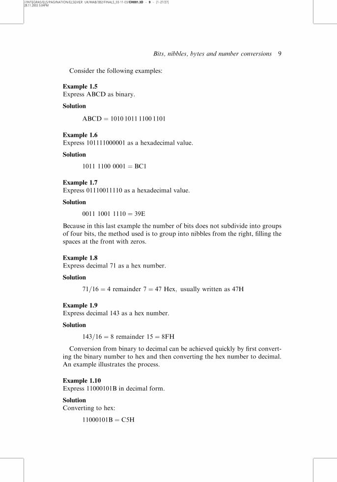
1.5 Inside microcontrollers
Microcontrollers normally contain RAM, ROM (EEPROM, EPROM,PROM), logic circuits designed to do specific tasks (UART, I2C, SPI) andsquare-wave oscillator (clock).
Built from the logic circuitry the microcontroller has two parts, the processorcore and the onboard peripherals. See Figure 1.3.
RAM locations that have special functions and support the processor coreand onboard peripheral circuitry are called special function registers (SFRs)and are reserved areas.
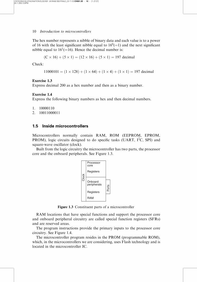
The program instructions provide the primary inputs to the processor corecircuitry. See Figure 1.4.
The microcontroller program resides in the PROM (programmable ROM),which, in the microcontrollers we are considering, uses Flash technology and islocated in the microcontroller IC.
Processorcore
Registers
Onboardperipherals
Registers
RAM
Por
ts
Clo
ck
Figure 1.3 Constituent parts of a microcontroller
10 Introduction to microcontrollers
//INTEGRAS/ELS/PAGINATION/ELSEVIER UK/MAB/3B2/FINALS_03-11-03/CH001.3D – 11 – [1–27/27]28.11.2003 5:04PM
1.6 Microcontroller programming
The microcontroller program comprises a set of instructions written by theprogram designer. There are four classes of instructions:
1. Arithmetic operations2. Logic operations3. Data transfer operations4. Branch operations.
ARITHMETIC OPERATIONS
Arithmetic instructions operate on whole numbers only and support addition,subtraction, multiplication and division.
Addition
ADD A,#66H ; add the hex number 66 to the accumulator A
This is an example of immediate addressing.The # sign is important, if it were omitted the operation would have a
different meaning.
ADD A,66H ; add to accumulator A the contents of RAM address; 0066H
This is an example of direct addressing.Accumulator A is an SFR; it is an 8-bit register and its RAM address is
00E0H. A large number of instructions use accumulator A, but not all.
INC 66H ; increment (add 1) the contents of address 0066H
Exercise 1.5
Is there any difference between the following two instructions?A) INC A B) ADD A,#1
Microcontrollerprogram
Instructiondecoder
Processorcore
Onboardperipherals
Clock oscillatorcircuitry
SFR RAM SFR
Por
ts
Figure 1.4 Block diagram of a microcontroller
Microcontroller programming 11
//INTEGRAS/ELS/PAGINATION/ELSEVIER UK/MAB/3B2/FINALS_03-11-03/CH001.3D – 12 – [1–27/27]28.11.2003 5:04PM
Subtraction
SUBB A, #66H ; subtract hex66 from the contents of A
The extra B in the instruction implies Borrow. If the contents of A are less thanthe number being subtracted then bit 7 of the program status word (PSW)SFR will be set. (For details of the PSW and other SFRs, see Appendix C.)
DEC A ; decrement A by 1, put result into A
Exercise 1.6
Is there any difference between the following two instructions?
(1) DEC A (2) SUBB A,#1
Multiplication
MUL AB ; multiply the contents of A and B, put the answer in AB
A is the accumulator and B is another 8-bit SFR provided for use with theinstructions multiply and divide. A and B are both 8-bit registers. The productof the multiplication process could be a 16-bit answer.
Example 1.11A ¼ 135 decimal, B ¼ 36 decimal. What would be the value in each registerafter executing the instruction MUL AB?
Solution
A� B ¼ 4860 ¼ 0001 0010 1111 1100B ¼ 12FCH0001 0010 or 12H would be placed in A; 1111 1100 or FCH in B
Exercise 1.7
If A ¼ 2FH and B ¼ 02H, what would each register contain after execution ofthe instruction MUL AB?
Division
DIV AB ; divide A by B, put quotient in A and remainder in B
Example 1.12
A ¼ 135, B ¼ 36. What would be the value in each register after execution ofthe instruction DIV AB?
Solution
Decimal values are assumed if the value quoted is not followed by an H
A=B ¼ 3; remainder 27 ð27 ¼ 1BHÞ: Hence 03H in A, 1BH in B
If multiplication or division is not being used then register B, which is bitaddressable, can be used as a general-purpose register.
12 Introduction to microcontrollers
//INTEGRAS/ELS/PAGINATION/ELSEVIER UK/MAB/3B2/FINALS_03-11-03/CH001.3D – 13 – [1–27/27]28.11.2003 5:04PM
Exercise 1.8
If A ¼ 2FH and B ¼ 02H, what would each register contain after the executionof the instruction DIV AB?
LOGIC OPERATIONS
The set of logic functions include:
ANL AND LogicORL OR LogicXRL exclusive OR LogicCPL Complement (i.e. switch to the opposite logic level)RL Rotate Left (i.e. shift byte left)RR Rotate Right (i.e. shift byte right)SETB Set bit to logic 1CLR Clear bit to logic 0
AND operation
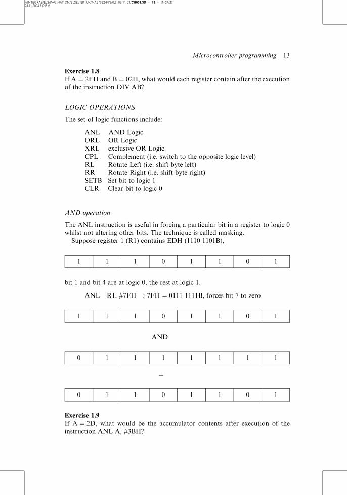
The ANL instruction is useful in forcing a particular bit in a register to logic 0whilst not altering other bits. The technique is called masking.
Suppose register 1 (R1) contains EDH (1110 1101B),
1 1 1 0 1 1 0 1
bit 1 and bit 4 are at logic 0, the rest at logic 1.
ANL R1, #7FH ; 7FH ¼ 0111 1111B, forces bit 7 to zero
1 1 1 0 1 1 0 1
AND
0 1 1 1 1 1 1 1
¼
0 1 1 0 1 1 0 1
Exercise 1.9
If A ¼ 2D, what would be the accumulator contents after execution of theinstruction ANL A, #3BH?
Microcontroller programming 13
//INTEGRAS/ELS/PAGINATION/ELSEVIER UK/MAB/3B2/FINALS_03-11-03/CH001.3D – 14 – [1–27/27]28.11.2003 5:04PM
ORL operation
Another aspect of masking is to use the ORL instruction to force a particularbit to logic 1, whilst not altering other bits.
The power control (PCON) SFR in the 8051 family, is not bit addressableand yet has a couple of bits that can send the microcontroller into idle mode orpower down mode, useful when the power source is a battery.
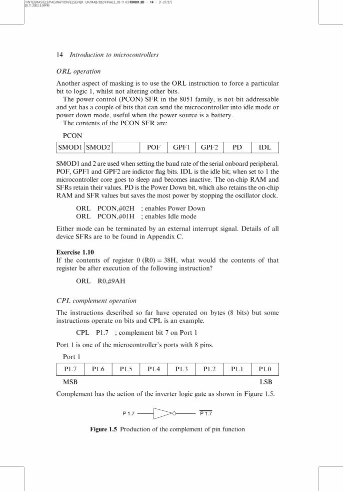
The contents of the PCON SFR are:
PCON
SMOD1 SMOD2 POF GPF1 GPF2 PD IDL
SMOD1 and 2 are used when setting the baud rate of the serial onboard peripheral.POF, GPF1 and GPF2 are indictor flag bits. IDL is the idle bit; when set to 1 themicrocontroller core goes to sleep and becomes inactive. The on-chip RAM andSFRs retain their values. PD is the Power Down bit, which also retains the on-chipRAM and SFR values but saves the most power by stopping the oscillator clock.
ORL PCON,#02H ; enables Power DownORL PCON,#01H ; enables Idle mode
Either mode can be terminated by an external interrupt signal. Details of alldevice SFRs are to be found in Appendix C.
Exercise 1.10
If the contents of register 0 (R0) ¼ 38H, what would the contents of thatregister be after execution of the following instruction?
ORL R0,#9AH
CPL complement operation
The instructions described so far have operated on bytes (8 bits) but someinstructions operate on bits and CPL is an example.
CPL P1.7 ; complement bit 7 on Port 1
Port 1 is one of the microcontroller’s ports with 8 pins.
Port 1
P1.7 P1.6 P1.5 P1.4 P1.3 P1.2 P1.1 P1.0
MSB LSB
Complement has the action of the inverter logic gate as shown in Figure 1.5.
P 1.7 P 1.7
Figure 1.5 Production of the complement of pin function
14 Introduction to microcontrollers
//INTEGRAS/ELS/PAGINATION/ELSEVIER UK/MAB/3B2/FINALS_03-11-03/CH001.3D – 15 – [1–27/27]28.11.2003 5:04PM
Exercise 1.11
If the contents of port 0 (P0) ¼ 125, what would be the port contents afterexecution of the following instruction?
CPL P0
RL, rotate left one bit, RR, rotate right one bit operations
Suppose the accumulator A contents are 0000 0001B; this is 01H.
RL A ; contents of A become 0000 0010B or 02HRL A ; 0000 0100B or 04HRL A ; 0000 1000B or 08H
RL three times has the effect of multiplying A by 23 i.e. by 8.Suppose the accumulator A contents are 1000 0000B, or 128 decimal, then:
RR A ; contents of A become 0100 0000B which is 64 decimalRR A ; A becomes 0010 0000B=32 decimalRR A ; A becomes 0001 0000B=16 decimalRR A ; A becomes 0000 1000B=8 decimal
RR four times has the same effect as dividing A by 24 i.e. 16.
128
16¼ 8
Exercise 1.12
If the content of A is 128 and B is 2, what would the register contents be afterexecution of the following instructions?
RR ARL BRR ARR ARL B?
SETB set bit, CLR clear bit operations
This instruction operates on a bit, setting it to logic 1.
SETB P1.7 ; set bit 7 on Port 1 to logic 1
Consider Figure 1.6 where pin 7 of port 1 is connected as shown.SETB P1.7 puts logic 1 (e.g. 5 V) onto the inverter input and therefore its
output, the LED cathode, is at 0V causing current to flow through the LED.The LED has a particular forward voltage Vf (refer to component specificatione.g. www.farnell.com).
Microcontroller programming 15
//INTEGRAS/ELS/PAGINATION/ELSEVIER UK/MAB/3B2/FINALS_03-11-03/CH001.3D – 16 – [1–27/27]28.11.2003 5:04PM
Typically Vf ¼ 2:2V and forward current If ¼ 8mA so that:
R¼ 5V�Vf
If¼ 5� 2:2
8� 10�3¼ 2:8� 1000
8¼ 350�¼ 330� (preferred value)
CLR P1.7 ; clears bit 7 on port 1 to zero
CLR P1.7 puts logic 0 on the inverter gate input and therefore its output, theLED cathode, becomes logic 1 which is 5V. This gives a voltage difference(5V DC� cathode voltage) of 0V and the LED turns off.
The inverter gate in the above circuit provides a good current bufferprotecting the microcontroller port pin from unnecessary current loading.In the above circuit the current flow is between the inverter gate and the 5VDC supply.
If an inverter gate is not used to drive a LED then the control may be directlyfrom the port pin but this will demand a current in milliamps from the port pin.
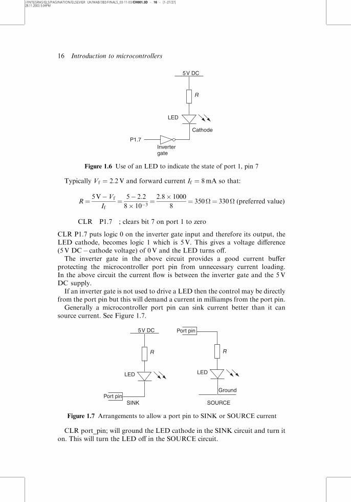
Generally a microcontroller port pin can sink current better than it cansource current. See Figure 1.7.
CLR port_pin; will ground the LED cathode in the SINK circuit and turn iton. This will turn the LED off in the SOURCE circuit.
5 V DC
R
LED
Cathode
Invertergate
P1.7
Figure 1.6 Use of an LED to indicate the state of port 1, pin 7
5 V DC
R
LED
SINKPort pin
Port pin
R
LED
Ground
SOURCE
Figure 1.7 Arrangements to allow a port pin to SINK or SOURCE current
16 Introduction to microcontrollers
//INTEGRAS/ELS/PAGINATION/ELSEVIER UK/MAB/3B2/FINALS_03-11-03/CH001.3D – 17 – [1–27/27]28.11.2003 5:04PM
SETB port_pin; will put logic 1 on the LED cathode in the SINK circuit andturn it off. This will turn the LED on in the SOURCE circuit.
Exercise 1.13
If Vcc ¼ 5V and for an LED, Vf ¼ 0:7V and the pin P0.0 of the microcon-troller port can sink 10mA and source 50 mA.
1. How you connect the LED to the microcontroller and2. Calculate the value of series resistor R.
Data transfer operations
This is mainly concerned with transfer of data bytes (8 bits). SETB and CLRhave just been covered; they operate on bits.
MOV operation
MOV moves bytes of data. Consider driving a seven-segment display (decimalpoint dp included) where each LED is driven by the sink method. See Figure 1.8.
Each LED illuminates a segment. The seven-segment display is shown to theright with its standard segment identification letters.
Example 1.13
Write two program lines, one to display 3, the second to display 4. In both casesturn the decimal point off.
Solution
P1.7 P1.6 P1.5 P1.4 P1.3 P1.2 P1.1 P1.0
dp g f e d c b a
3 1 0 1 1 0 0 0 0 B0H
4 1 0 0 1 1 0 0 1 99H
5 V DC
R
P1.7
5 V DC
R
P1.6
5 V DC
R
P1.5
5 V DC
R
P1.4
5 V DC
R
P1.3
5 V DC
R
P1.2
5 V DC
R
P1.1
5 V DC
R
P1.0
dp g f e d c b a
a
b
c
gf
ed
dp
Figure 1.8 Arrangement for a seven-segment LED display
Microcontroller programming 17
//INTEGRAS/ELS/PAGINATION/ELSEVIER UK/MAB/3B2/FINALS_03-11-03/CH001.3D – 18 – [1–27/27]28.11.2003 5:04PM
MOV P1,#B0H ; display 3MOV P1,#99H ; display 4
Note: MOV P1,#B0H would give a syntax error. In common with a numberof cross assemblers the software would see B0H as a label because it starts witha hex symbol; 99H would be acceptable since it starts with a number. Thecorrect program line should be MOV P1,#0B0H i.e. a zero must be placed infront of the hex symbol.
The instruction MOV is used to move RAM data that is onboard themicrocontroller.
Examples
MOV 0400H,#33H ;move the number 33 hex toRAMaddress 0400 hexMOV A,P1 ; move the contents of port 1 to accumulator AMOV R0,P3 ; move the contents of port 3 into register R0
Note: As well as the accumulator A the microcontroller has 32 registers infour banks of eight in the processor core. These 32 bytes are fast RAM andshould be used in preference to standard onboard RAM.
Each of the banks contain 8 registers R7, R6, R5, R4, R3, R2, R1, R0. Thereare four banks: 0, 1, 2 and 3.
Bank 0 is the default bank; the other banks can be selected by two bits(RS1,RS0) in the program status word (PSW) SFR
PSW
CY AC F0 RS1 RS0 OV F1 P
0 0 Register bank 0 (default)
0 1 Register bank 1
1 0 Register bank 2
1 1 Register bank 3
Other PSW bits are indicator flags:
CY (carry flag)AC (auxiliary carry flag)OV (overflow flag)P (parity flag)F0, F1 (general-purpose user-defined flags)
More information on the register banks and the SFRs can be found inAppendix C. MOVX is used to move data between the microcontroller andthe external RAM. MOVC is used to move data (e.g. table data) from PROM(also called code memory) to RAM.
18 Introduction to microcontrollers
//INTEGRAS/ELS/PAGINATION/ELSEVIER UK/MAB/3B2/FINALS_03-11-03/CH001.3D – 19 – [1–27/27]28.11.2003 5:04PM
Exercise 1.14
Write an instruction to select the register bank 2 of the microcontroller.
Branch operations
There are two types, unconditional and conditional branching. Unconditionalbranch operations are
ACALL absolute callLCALL long call
ACALL calls up a subroutine, the subroutine must always have RET as its lastoperation. ACALL range is limited to þ127 places forward or �128 placesbackward. If your program jumps further than ACALL the compiler willreport that the program is jumping out of bounds and replacement by LCALLwill solve the problem.
ACALL is two bytes long, LCALL is three bytes long.
AJMP absolute jumpLJMP long jumpSJMP short jump
Similar to ACALL and LCALL, AJMP and LJMP jump to addresses whereasSJMP, which has a similar range to ACALL and AJMP, jumps a number ofplaces.
The difference could be seen in the machine code. Consider the program:
$INCLUDE (REG66X.INC) ; lists all sfr addressesORG 0 ; sets start address to 0SJMP START ; short jump to START labelORG 0040H ; puts next program line at address 0040H
START: SETB P1.7 ; set pin 7 on port 1 to logic 1CLR P1.7 ; clear pin 7 on port 1 to logic 0AJMP START ; jump back to START labelEND ; no more assembly language
The machine code can be viewed in the list file, progname.lst:
SJMP STARTShows as 803E 80 is the hex for instruction SJMP
3E is the relative jump to reach 0040H where START is; itjumps from address 0002, the address after SJMP START,0002þ 3E ¼ 0040H
AJMP STARTShows as 0140 01 is the hex for instruction AJMP
40 is short for address 0040
Microcontroller programming 19
//INTEGRAS/ELS/PAGINATION/ELSEVIER UK/MAB/3B2/FINALS_03-11-03/CH001.3D – 20 – [1–27/27]28.11.2003 5:04PM
If LJMP had been used instead of AJMP then,LJMP STARTShows as 020040 02 is the hex for instruction LJMP
0040 is the full address
Exercise 1.15
In your own words describe the difference between ACALL and AJMP instruc-tions.Conditional branch operations:
JZ Jump if zeroJNZ Jump if not zeroDJNZ Decrement and jump if not zero
Consider an example (a subroutine called by ACALL):
DELAY: MOV R0,#34 ; move decimal 34 into register R0TAKE: DJNZ R0,TAKE ; keep subtracting 1 from R0 until zeroRET ; return from subroutine
CJNE Compare and jump if not equalConsider:
DELAY: MOV R0,#34 ; move decimal 34 into register R0TAKE: DEC R0 ; decrement R0
CJNE R0,#12,TAKE ; compare R0 with 12 jump to TAKE if notRET ; return when R0 equals 12
Other instructions are:
JC jump if carry is 1JNC jump if carry is 0
JB jump if bit ¼ 1JNB jump if bit ¼ 0
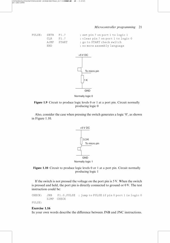
Consider a practical example of testing switched logic levels. Refer to Figure 1.9.If the switch is not pressed the voltage on the port pin is 0V. When the switchis pressed and held, then the port pin is connected directly to 5V. To test forswitch being pressed, the following program could be used:
$INCLUDE (REG66X.INC) ; lists all sfr addressesORG 0 ; sets start address to 0SJMP START ; short jump to START labelORG 0040H ; putsnextprogramlineataddress0040H
START: JB P1.0,PULSE ; jump to PULSE if pin 0 port 1 is logic 1CLR P1.7 ; otherwise clear pin 7 port 1 to zeroSJMP START ; go to START check switch
20 Introduction to microcontrollers
//INTEGRAS/ELS/PAGINATION/ELSEVIER UK/MAB/3B2/FINALS_03-11-03/CH001.3D – 21 – [1–27/27]28.11.2003 5:04PM
PULSE: SETB P1.7 ; set pin 7 on port 1 to logic 1CLR P1.7 ; clear pin 7 on port 1 to logic 0AJMP START ; go to START check switchEND ; no more assembly language
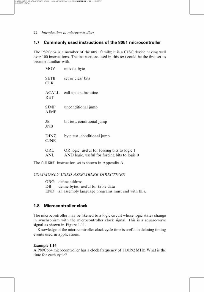
Also, consider the case when pressing the switch generates a logic ‘0’, as shownin Figure 1.10.
If the switch is not pressed the voltage on the port pin is 5V. When the switchis pressed and held, the port pin is directly connected to ground or 0V. The testinstruction could be:
CHECK: JNB P1.0,PULSE ; jump to PULSE if pin 0 port 1 is logic 0SJMP CHECK
PULSE:
Exercise 1.16
In your own words describe the difference between JNB and JNC instructions.
+5 V DC
To micro pin
1 K
Normally logic 0
GND
Figure 1.9 Circuit to produce logic levels 0 or 1 at a port pin. Circuit normallyproducing logic 0
+5 V DC
3.3 K
To micro pin
GND
Normally logic 1
Figure 1.10 Circuit to produce logic levels 0 or 1 at a port pin. Circuit normallyproducing logic 1
Microcontroller programming 21
//INTEGRAS/ELS/PAGINATION/ELSEVIER UK/MAB/3B2/FINALS_03-11-03/CH001.3D – 22 – [1–27/27]28.11.2003 5:04PM
1.7 Commonly used instructions of the 8051 microcontroller
The P89C664 is a member of the 8051 family; it is a CISC device having wellover 100 instructions. The instructions used in this text could be the first set tobecome familiar with.
MOV move a byte
SETB set or clear bitsCLR
ACALL call up a subroutineRET
SJMP unconditional jumpAJMP
JB bit test, conditional jumpJNB
DJNZ byte test, conditional jumpCJNE
ORL OR logic, useful for forcing bits to logic 1ANL AND logic, useful for forcing bits to logic 0
The full 8051 instruction set is shown in Appendix A.
COMMONLY USED ASSEMBLER DIRECTIVES
ORG define addressDB define bytes, useful for table dataEND all assembly language programs must end with this.
1.8 Microcontroller clock
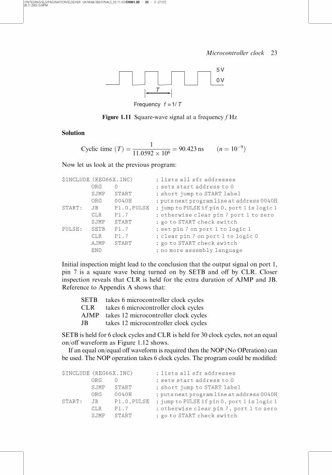
The microcontroller may be likened to a logic circuit whose logic states changein synchronism with the microcontroller clock signal. This is a square-wavesignal as shown in Figure 1.11.
Knowledge of the microcontroller clock cycle time is useful in defining timingevents used in applications.
Example 1.14
A P89C664 microcontroller has a clock frequency of 11.0592MHz. What is thetime for each cycle?
22 Introduction to microcontrollers
//INTEGRAS/ELS/PAGINATION/ELSEVIER UK/MAB/3B2/FINALS_03-11-03/CH001.3D – 23 – [1–27/27]28.11.2003 5:04PM
Solution
Cyclic time ðTÞ ¼ 1
11:0592� 106¼ 90:423 ns ðn ¼ 10�9Þ
Now let us look at the previous program:
$INCLUDE (REG66X.INC) ; lists all sfr addressesORG 0 ; sets start address to 0SJMP START ; short jump to START labelORG 0040H ; putsnextprogramlineataddress0040H
START: JB P1.0,PULSE ; jump to PULSE if pin 0, port 1 is logic 1CLR P1.7 ; otherwise clear pin 7 port 1 to zeroSJMP START ; go to START check switch
PULSE: SETB P1.7 ; set pin 7 on port 1 to logic 1CLR P1.7 ; clear pin 7 on port 1 to logic 0AJMP START ; go to START check switchEND ; no more assembly language
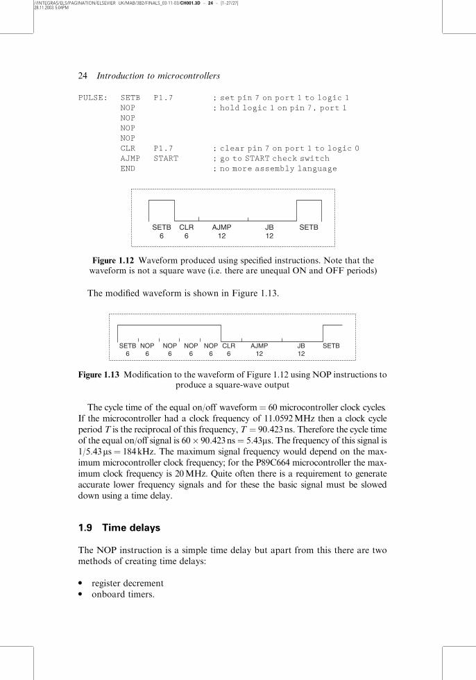
Initial inspection might lead to the conclusion that the output signal on port 1,pin 7 is a square wave being turned on by SETB and off by CLR. Closerinspection reveals that CLR is held for the extra duration of AJMP and JB.Reference to Appendix A shows that:
SETB takes 6 microcontroller clock cyclesCLR takes 6 microcontroller clock cyclesAJMP takes 12 microcontroller clock cyclesJB takes 12 microcontroller clock cycles
SETB is held for 6 clock cycles and CLR is held for 30 clock cycles, not an equalon/off waveform as Figure 1.12 shows.
If an equal on/equal off waveform is required then the NOP (No OPeration) canbe used. The NOP operation takes 6 clock cycles. The program could be modified:
$INCLUDE (REG66X.INC) ; lists all sfr addressesORG 0 ; sets start address to 0SJMP START ; short jump to START labelORG 0040H ; putsnextprogramlineataddress0040H
START: JB P1.0,PULSE ; jump to PULSE if pin 0, port 1 is logic 1CLR P1.7 ; otherwise clear pin 7, port 1 to zeroSJMP START ; go to START check switch
T
Frequency f = 1/ T
5 V
0 V
Figure 1.11 Square-wave signal at a frequency f Hz
Microcontroller clock 23
//INTEGRAS/ELS/PAGINATION/ELSEVIER UK/MAB/3B2/FINALS_03-11-03/CH001.3D – 24 – [1–27/27]28.11.2003 5:04PM
PULSE: SETB P1.7 ; set pin 7 on port 1 to logic 1NOP ; hold logic 1 on pin 7, port 1NOPNOPNOPCLR P1.7 ; clear pin 7 on port 1 to logic 0AJMP START ; go to START check switchEND ; no more assembly language
The modified waveform is shown in Figure 1.13.
The cycle time of the equal on/off waveform¼ 60 microcontroller clock cycles.If the microcontroller had a clock frequency of 11.0592MHz then a clock cycleperiod T is the reciprocal of this frequency, T ¼ 90:423ns. Therefore the cycle timeof the equal on/off signal is 60� 90:423ns¼ 5:43ms. The frequency of this signal is1/5:43ms¼ 184kHz. The maximum signal frequency would depend on the max-imum microcontroller clock frequency; for the P89C664 microcontroller the max-imum clock frequency is 20MHz. Quite often there is a requirement to generateaccurate lower frequency signals and for these the basic signal must be sloweddown using a time delay.
1.9 Time delays
The NOP instruction is a simple time delay but apart from this there are twomethods of creating time delays:
. register decrement
. onboard timers.
SETB6
SETBCLR6
AJMP12
JB12
Figure 1.12 Waveform produced using specified instructions. Note that thewaveform is not a square wave (i.e. there are unequal ON and OFF periods)
SETB6
NOP6
NOP6
NOP6
NOP6
CLR6
AJMP12
JB12
SETB
Figure 1.13 Modification to the waveform of Figure 1.12 using NOP instructions toproduce a square-wave output
24 Introduction to microcontrollers
//INTEGRAS/ELS/PAGINATION/ELSEVIER UK/MAB/3B2/FINALS_03-11-03/CH001.3D – 25 – [1–27/27]28.11.2003 5:04PM
The use of onboard timers will be described in a later chapter; here the registerdecrement method will be described.
The basic single loop program lines are:
DELAY: MOV R0,#number ; move a number into an 8-bit; register R0
TAKE: DJNZ R0,TAKE ; keep decrementing R0 until it is; zero
RET ; return from DELAY subroutine
MOV takes 6 clock cycles, DJNZ and RET each take 12 clock cycles. The delayis called up from the main program using ACALL, which takes 12 clock cycles.The delay time is (12þ 6þ (number� 12)þ 12) clock cycles. When the num-ber is small the NOPs (total 24 cycles) should be included,
Delay time ¼ ð24þ 12þ 6þ ðnumber� 12Þ þ 12Þ clock cycles
Delay time ¼ ð54þ ð12� numberÞÞ clock cycles
Example 1.15
A P89C664 microcontroller has an 11.0592MHz crystal-controlled clock oscil-lator. Write an assembly language program that will generate a 5 kHz square-wave signal on pin 7 of port 1 when a switch causes pin 0 on the same port to goto logic 1.
Solution
Clock frequency ¼ 11:0592MHzThus period of clock cycle ¼ ð1=11:0592MHzÞ ¼ 90:423 nsSignal frequency ¼ 5 kHzTherefore period of signal cycle ¼ ð1=5 kHzÞ ¼ 200 ms
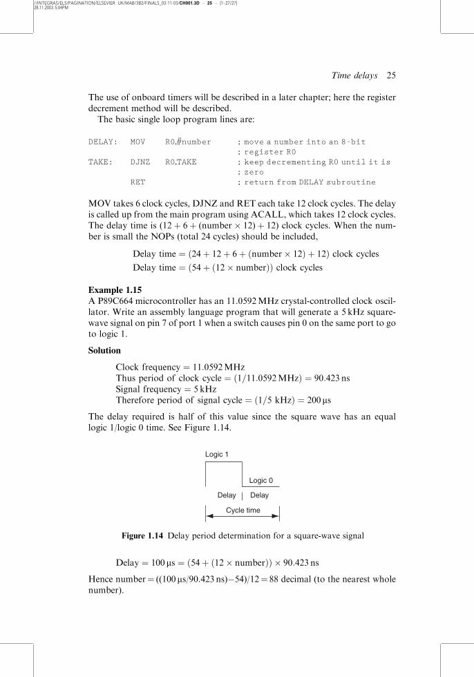
The delay required is half of this value since the square wave has an equallogic 1/logic 0 time. See Figure 1.14.
Delay ¼ 100 ms ¼ ð54þ ð12� numberÞÞ � 90:423 ns
Hence number¼ ((100 ms/90.423 ns)�54)/12¼ 88 decimal (to the nearest wholenumber).
Logic 1
Logic 0
Delay Delay
Cycle time
Figure 1.14 Delay period determination for a square-wave signal
Time delays 25
//INTEGRAS/ELS/PAGINATION/ELSEVIER UK/MAB/3B2/FINALS_03-11-03/CH001.3D – 26 – [1–27/27]28.11.2003 5:04PM
$INCLUDE (REG66X.INC) ; lists all sfr addressesORG 0 ; sets start address to 0SJMP START ; short jump to START labelORG 0040H ; putsnextprogramlineataddress0040H
START: JB P1.0,PULSE ; jump to PULSE if pin 0, port 1 is logic 1CLR P1.7 ; otherwise clear pin 7, port 1 to zeroSJMP START ; go to START check switch
PULSE: SETB P1.7 ; set pin 7 on port 1 to logic 1ACALL DELAYNOP ; hold logic 1 on pin 7 port 1NOPNOPNOPCLR P1.7 ; clear pin 7 on port 1 to logic 0ACALL DELAYAJMP START ; go to START check switch
DELAY: MOV R0,#88TAKE: DJNZ R0,TAKE
RETEND ; no more assembly language
The delay depended on the chosen microcontroller clock frequency and in theexample this was 11.0592MHz. This apparently unusual number gives standardbaud rate values, which will be useful later. For microcontroller clock frequen-cies in this region the single loop register decrement method gives delays in theregion of microseconds. Generally a double loop gives delays in the region ofmilliseconds and a triple loop delay gives delays in the region of seconds.
Exercise 1.17
Using the techniques above, assuming the clock frequency is 11.0592MHz, writea program to generate a pulse of 20kHz on pin 7 of port 1 of the microcontroller.
DOUBLE LOOP DELAY
DELAY: MOV R1,#number1INNER: MOV R0,#number2TAKE: DJNZ R0,TAKE
DJNZ R1,INNERRET
Approximately the time delay¼ (number 1)� (number 2)� 12 clock cycle periods.For example, suppose number 1¼ 200 and number 2¼ 240 and 1 clockcycle¼ 90.423 ns.
Time delay ¼ 200� 240� 12� 90:423 ns ¼ 52:1ms
The bigger the values of number 1 and number 2, the better the approximation.The software used has simulation and the values of number 1 and number 2 canbe fine tuned to give the accurate delay during simulation.
26 Introduction to microcontrollers
//INTEGRAS/ELS/PAGINATION/ELSEVIER UK/MAB/3B2/FINALS_03-11-03/CH001.3D – 27 – [1–27/27]28.11.2003 5:04PM
TRIPLE LOOP DELAY
DELAY: MOV R2,#number1OUTER: MOV R1,#number2INNER: MOV R0,#number3TAKE: DJNZ R0,TAKE
DJNZ R1,INNERDJNZ R2,OUTERRET
Approximately the delay=(number 1)� (number 2) � (number 3)�12 clockcycle periods. Suppose number 1=40, number 2=200, number 3=240, 1 clockcycle period=90.423 ns.
Delay ¼ ð40� 200� 240� 12� 90:423Þ ns � 2 s
Long enough to see a LED going on and off.In later chapters the use of the microcontroller’s onboard timers will be used
to describe an alternative method of producing time delays. The timer methodwill require the configuration of the timer SFRs.
The register decrement method described above is a valid alternative, easy toimplement and does not require the configuration of SFRs.
Summary
. A microcontroller is a computer with most of the necessary support chipsonboard. Microcontrollers can be embedded and are available in a varietyof forms to suit practical applications.
. Number systems, such as binary and hexadecimal, are used in microcon-troller applications. If decimal numbers are required they can be convertedto binary and/or hexadecimal and vice versa.
. There are four classes of instructions namely: arithmetic, logical, datatransfer and branch instructions.
. The microcontroller port pins may be required to sink and source currents.
. Time delays may be achieved by using register decrement instructions or byusing onboard timer circuits.
. Using register decrement, longer delays can be achieved by the use of doubleor triple loops.
Summary 27


