Embed Size (px)
Citation preview
1995 SecondModulator-Klystron Workshop
A Modulator-Klystron Workshopfor Future Linear Colliders
Organizing Committee:
A.R. Donaldson, ChairmanR.L. CasselP.D. PearceR. Lai, Workshop Administrator
Stanford Linear Accelerator CenterStanford University, Stanford, CaliforniaOctorber 9-11, 1995
SLAC-48 1tom-95 l0340--March 1996UC-414
-.
Prepared for the Department of Ener~under contract number DE-AC03-76SFO0515 //
/
Printed in the United States of America. Available from the Nation~ TechmcU.S. Department of Commerce, 5285 Port Royal Road, Springfield, Virginia 22.

Art Credits
The e- and e+ collision logo is the work of Terry Anderson,and the workshop photographs me by Dave FicMin.
ii

TABLE OF CONTENTS
Foreword . . . . . . . . . . . . . . . . . . . . . . . . . .. . . . . . . . . . . . . . . . . . . . . . . . . . . . . . . . . . . . . . . . . . . . . . . . . . . . . . . . . . . . . . . . . . . . . . . . . . . . . . . . . . . . . . ..l
Worhhop Conclmiom .. . . . . . . . . . . . . . . . . . . . . . . .. . . . . . . . . . . . . . . . . . . . . . . . . . . . . . . . . . . . . . . . . . . . . . . . . . . . . . . . . . . . . . . . . . . . . . . ...2
Industrid Sponsors . . . . . . . . . . . . . . . . . . . . . . . . . . . . . . . . . . . . . . . . . . . . . . . . . . . . . . . . . . . . . . . . . . . .. . . . . . . . . . . . . . . . . . . . . . . . . . . . . . . . . . 4
~eNext Lkem Collider RF System .. R. Ruth. . . . . . . . . . . . . . . . . . . .. . . . . . . . . . . . . . . . . . . . . . . . . . . . . . . . . . . . . . . . . . . . . . ...5
Summary of TRC Report on WystrotiModdator Requirements for FutureLmear Colliders --P. Wihon . . . . . . . . . . . . . . . . . . . . . . . . . . . . . . . . . . . . . . . . . . . . . . . . . . . . . . . . . . . . . . . . . . . . . . . . . . . . . . . . . . . . . . . . . . . . . . . . . . . . ...28
Development and Advances in Conventional High Power RF Systems -- P. Wihon . . . . . . . . . . . . . . . . . . . . . . . . . 45
Moddator-P.S. Parameter Space for Future Linear Colliders --G. Ca~otAs. . . . . . . . . . . . . . . . . . . . . . . . . . . . ...51
Mystron Session Summary--S. ~M.., . . . . . . . . . . . . . . .. . . . . . . . . . . . . . . . . . . . .. . . . . . . . . . . . . . . . . . . . . . . . . . . . . . . . . . . . . . . . 71
Moddator Wystron iteration Issues --E. Wright . . . . . . . . . . . . . . . . . . . . . . . . . . . . . . . . . . . . . . . . . . . . . . . . . . . . . . . . . . . . . ...72
NLC Wystron Moddator-- R. L. Cassel . . . . . . . .. . . . . . . . . . . . . . . . . . . . . . . . . . . . . . . . . . . . . . . . . . . . . . . . . . . . . . . . . . . . . . . . . . . 81
Mse Moddator Using a PFL and Magnetic Switch--M. Memoto . . . . . . . . . . . . . . . . . . . . . . . . . . . . . . . . . . . . . . . . . . 126
R&D of the C-Band Mystron Moddator --~ H. Baba, T. Shint&e, K. Wat&e,J. S. Oh, P. Pearce, M. H. Cho, W. Natiung . . . . . . . . . . . . . . . . . . . . . . . . . . . . . . . . . . . . . . . . . . . . . . . . . . . . . . . 138
Moddators mdSwitched Mode P.S. --G. Bees . . . . . . . . . . . . . . . . . . . . . . . . . . . . . . . . . . . . . . . . . . . . . . . . . . . . . . . . . . . . . . . ..l48
Moddator Efficiency, Ringing, PFL’svs PFN’s --T. Burkes . . . . . . . . . . . . . . . . . . . . . . . . . . . . . . . . . . . . . . . . . . . . . . . ..l54
Compact &Efficient MMtiator Desi~.. J. Ditiel . . . . . . . . . . . . . . . . . . . . . . . . . . . . . . . . . . . . . . . . . . . . . . . . . . . . . . . . . . ..l59
Sm~of Mtitiator Efficiency Session .. G. Lqh . . . . . . . . . . . . . . . . . . . . . . . . . . . . . . . . . . . . . . . . . . . . . . . . . . . . . . . . ..l~
Romd Table Discussion of Mtidator Pmmeters .. G. Lqh . . . . . . .. . . . . . . . . . . . . . . . . . . . . . . . . . . . . . . . . . . . . . . . ..l62
Moddator Efficiency vsCost --H. fleffer . . . . . . . . . . . . . . . . . . . . . . . . . . . . . . .. . . . . . . . . . . . . . . . . . . . . . . . . . . . . . . . . . . . . . . . . 164
Modtiator Construction for Linear Collider Wystrons -- ~ s. GOU .. . . . . . . . . . . . . . . . . . . . . . . . . . . ...166
Recent Performance of Mystron Testing Moddators in the SLAC Wystron Test hbR. Koontz, S. Goti, J. Eichner . . . . . . . . . . . . . . . . . . . . . . . . . .. . . . . . . . . . . . . . . . . . . . . . . . . . . . . . . . . . . . . . . . . . . . . . ..l89
Bltiein PFN’s for 100 MW Class X-Band Wystrons --H. Mizuw . . . . . . . . . . . . . . . . . . . . . . . . . . . . . . . . . . . . . . . . ..l92
DESY Hard Tube Modtiator Tests--S. Choroba . . . . . . . . . . . . . . . . . . . . . . . . . . . . . . . . . . . . . . . . . . . . . . . . . . . . . . . . . . . . . ..2O8
Commissioning of the Hard Tube Wser Experiment at DESY --M. Bieler, S. Choroba,J. Hameister, H.- Ch. Lewin, R. Giebeler, S. &ti . . . . . . . . . . . . . . . . . . . . . . . . . . . . . . . . . . . . . . . . . . . . . . . . . ..22l
Triaxid Helical Bltiein Type Moddator --H. ShiAra . . . . . . . . . . . . . . . . . . . . . . . . . . . . . . . . . . . . . . . . . . . . . . . . . . . ...224
Moddator Construction Session Summary --J. Grippe . . . . . . . . . . . . . . . . . . . . . . . . . . . . . . . . . . . . . . . . . . . . . . . . . . . . . . . 228
ThomsonHigh Stability&Large Duty Cyle Moddators -- R. Lechatellier ..... .............. .............229
Upgradingthe CTFModdators toa Peak OutputPower--P. Pearce . . . . . . . . . . . . . . . . . . . . . . . . . . . . . . . . . . . . ...244
Power Moddators Based on Advanced Transformer Li -- ~ M. Choi, M. Gu&ersen . . . . 250
Thyratron Lifetimes, A Brief Review -- G. D. Wa& M. J. Barnes . . . . . . . . . . . . . . . . . . . . . . . . . . . . . . . . . . . . . . . ...258
Thyratron Reliability and Lifetime --H. tinwaU .. . . . . . . . . . . . . . . . . . . . . . . . . . . . . . . . . . . . . . . . . . . . . . . . . . . . . . . . . . ...272
Continuous Operation of a 250 kW Thyratron --H. GrunwaU, J. McGowan, J. Creedon . . . . . . . . . . . . ...288
iii

Mtitiator Switch Session S~~.. D. Ficklin . . . . . . . . . . . . . . . . . . . . . . . . . . . . . . . . . . . . . . . . . . . . . . . . . . . . . . . . . . . . ...292
Pseudo-Spark Switch Development at CERN for the LHC Beam Dumping System --L. Ducimetiere, P. Faure, U. Jamsson, H. Riege, M. Schhug,
G. H. Schr~ert~ . . . . . . . . . . . . . . . . . . . . . . . . . . . . . . . . . . . . . . . . . . . . . . . . . . . . . . . . . . . . . . . . . . . . . ..2g3
Pseudospark, Back Lighted Thyratron Overview --M. Gundersen . . . . . . . . . . . . . . . . . . . . . . . . . . . . . . . . . . . . . . . . ...312
Switch Alternatives Summary-- V. Nesterov . . . . . . . . . . . .. . . . . . . . . . . . . . . . . . . . . . . . . . . . . . . . . . . . . . . . . . . . . . . . . . . . . . . ..3l9
Solid State Alternatives for Wystron Moddators -- M. J. Barnes, G. D. Wait. . . . . . . . . . . . . . . . . . . . . . . . . . . . . . 320
Summary: Solid State Switch Mternatives for ~ystron Moddators --M. Barnes . . . . . . . . . . . . . . . . . . . . . . . . . 339
EEV Thyratrons for NLC Wystron Modtiators -- R. SheUrake, C. R Weathemp, C. A. Pirne . . . . . ...341
SLAC Wystron Reliability --G. CaVot&is . . . . . . . . . . . . . . . . . . . . . . . .. . . . . . . . . . . . . . . . . . . . . . . . . . . . . . . . . . . . . . . . . . . . ..3M
AHisto~of tie~yratron Llfetfies at SLAC .. D. Ficklin . . . . . . . . . . . . . . . . . . . . . .. . . . . . . . . . . . . . . . . . . . . . . . . . . ..35l
Presentation: Review of LIL Wystron-Modtiator System Reliability -- P. Pearce . . . . . . . . . . . . . . . . . . . . . . .355
Review of LiL Wystron-Moddator System Reliability -- P. Pearce, G. McMomgle, G. Retiier ...,... 374
Reliability/Maintenance Issues of Wystrons and Thyratrons -- T. Shidara . . . . . . . . . . . . . . . . . . . . . . . . . . . . . . . . . . 380
Presentation: Wystron Moddator System Performance for PLS-- M. H. Cho. . . . . . . . . . . . . . . . . . . . . . . . . . . . . .389
~ystron Moddator System Performances for PLS 2-G --M, H. Cti, J. S. Oh,S. S. Park, W.Na&ng . . . . . . . . . . . . . . . . . . . . . . . . . . . . . . . . . . . . . . . . . . . . . . . . . . . . . . . . . . . . . . . . . . . . . . . . . . . . . . . . . . . 408
SLAC Mtiulator Reliabili~ .. J. AsMon . . . . . . . . . . . . . . .. . . . . . . . . . . . . . . . . . . . . . . . . . . . . . . . . . . . . . . . . . . . . . . . . . . . . . . . ..4l3
SLAC Moddator Availability and Impact on SLC Operations --A. R. Dona~on, J. Ashton . . . . . . . ...423
Reliability Summary --J. Sheppard, A. R. Do~tion . . . . . . . . . . . . . . . . . . . . . . . . . . . . . . . . . . . . . . . . . . . . . . . . . . . . . . . . . . 426
Presenwtion: Smart Modulator Technology --P. Pearce . . . . . . . . . . . . . . . . . . . . . . . . . . . . . . . . . . . . . . . . . . . . . . . . . . . . . 427
Smart Modtiator Technology --P. Pearce, G. McMo~gle . . . . . . . . . . . . . . . . . . . . . . . . . . . . . . . . . . . . . . . . . . . . . . . . . 437
Presentation: Diagnostic & Software System for CERN Moddators -- G. McMonagle . . . . . . . . . . . . . . . . . 442
Implementation of Diagnostic & Software System for CERN -- P. Pearce, G. McMowgle,
G. Rem.er . . . . . . . . . . . . . . . . . . . . . . . . . . . . . . . . . . . . . . . . . . . . . . . . . . . . . . . . . . . . . . . . . . . . . . . . . . . . . . . . . . . . . . . . . . . . . . . . ...458
Smart Modtiator Summary -- J. DeLamare . . . . . . . . . . . . . . . . . . . . . . . . . . . . . . .. . . . . . . . . . . . . . . . . . . . . . . . . . . . . . . . . . . . ...463
Autior Index . . . . . . . . . . . . . . . . . . . . . . . . . . . . . . . . . . . . . . . . . . . . . . . . . . . . . . . . . . . . . . . . . . . . . . . . . . . . . . . . . . . . . . . . . . . . . . . . . . . . . . . . . ..4M
Attendee List, affiliations and addresses . . . . . . . . . . . . . . . . . .. . . . . . . . . . . . . . . . . . . . . . . . . . . . . . . . . . . . . . . . . . . . . . . . . . . . . . . . 465
iv

FOWWO~
The frst Modulator-~ystron Workshop was held at CE~ in Octok 1991. It focused onimproving the operation and reliability of modulator-~ystron smtions in existing particle accel-erators. This second workshop examined the present state of modulator design and attemptdan extrapolation for future electron-positron tiear co~iders. These co~ders are currentiyviewd as mtitikilometer-long accelerators consisting of a thousand or more RF sources with5~ to 1~, or more, pulsed power systems. The workshop opened with two introductory@s that presented the current approaches to designing these hear colfiders, the mticipatedRF sources, and the design constraints for pulse power.
Thecost of mainAC poweris amajoreconomicconsiderationfor a futureco~ider,conse-quendytheworkshopinvestigateefficientmodulatordesigns.Techniquesthateffectivelyapplytheartof powerconversion,fromtie AC mainsto theRFoutput,andspecificdy,designsthatgenerateoutputpulseswithveryfastrisetimesascomparedto theflattop.
There were six sessions that involvd one or more presentations based on problems specific tothe design and production of thousands of modulator-tiystron stations, followd by discussionand debate on the material.
The session leaders were representative of modulator and Mystron designers and managers intie accelerator community. This degree of representation extendd to 2D of the workshopattendees. The otier in represent a commercid-industrid contingent involvd in the designand production of modulators, Uystrons, thyratrons, pulse &ansformers and other pulse powercomponents.
A beneficent fraction of the industrid contingent consisting of Triton Services, he., Titan-Beta, Stangenes hdustries, EEV and EG&G providti financial support for the workshop.Their sponsorship plus fiancid assistance from SLAC supportd the banquet, picnic, andrefreshment breaks. Their generosity was the basis for the social success and a signflcantfactor in the gened success of the workshop.
The absolute success of this assembly is difficult to gauge. We extid many importantissues: efficiency, performance, construction, refiabflity, diagnostics and the necessity ofmodulator-tiystron integration. But we dso left several questions or problems unresolvd. Theconclusions on the fo~owing pages offer an idea of what was answered and what was missed.Our work wdl eventually have an impact on linear co~der design. And even in our designdisagreements, we indicati what direction future investigations (workshops and actualresearch) must take.
The workshop organizers were Dick Cassel, Peter Pearce and the writer. Ruby Lai did asuperb job organizing the announcements, invitations, and registration as well as being thetitorid assistant. She dso arranged and coordinate the entire social scene for the work-shop. Justine Mello assisti Ms. Lai with the registration-attendance database and registration.AEtio Saab merits d credit for proposing SLAC as the site and host.
Oneother deti requires an explanation. The 1991 workshop was cdld a ~ystron-ModulatorTechnical Meeting. The workshop organizers have used K-M md M-K indiscriminately.However this writer prefers Modulator-~ystron Workshop. It is an extension of left to right(in to out), from tie WW plug, to the power supply, to the moddator and fmdly to theMystron. This volume is labeled tie Second Modulator-~ystron Workshop. I trust that PeterPearce, the organizer of the f~st meeting, wdl excuse me and understand my motive.
A.R. Donaldson
1
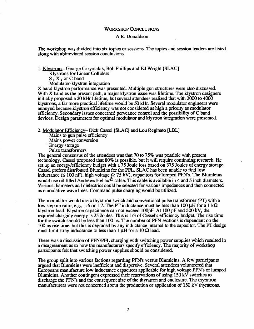
WORKSHOP COnfUSiOnS
A.R. Donaldson
The workshop was divided into six topics or sessions. The topics and session leaders are fistdalong with abbreviatti session conclusions.
1. ~ Gwrge Caryotakis, Bob PhilUps and M Wright [SLAC]~ystrons for Linear ColfidersS, X,or CbandModdator-Mystron integration
X band Uystron performance was presentd Multiple gun structures were dso discussd.With X band as the present path, a major Mystron issue was Metime. The Uystron designersinitiy proposal a 20 kHr lifetime, but several attendees ad that with 2000 to 4000Uys@ons, a far more practical tifetime would be 50 W. Seved moddator engineers wereannoyd &ause Mystron efficiency was not consideti as high a priority as modulatorefficiency. Secondary issues concernd perveance control and the possibility of C banddevices. Design parameters for optimal modulator and Uystron integration were presented.
2. Moddato Rffiaency.
– Dick Cassel [SLAq and Lou Reginato LBL]Mainsrm gun pulse efficiencyMains power conversionEnergy storageWse transformers
The general consensus of the attendees wm that 70 to 75% was possible with presenttechnology. Cassel proposal that 8090 is possible, but it will ~uire continuing research. Heset up an energy/efficiency budget with a 75 Jode loss based on 375 Joules of energy storage.Cassel prefers distibuti Blurrdeins for the PFL. SLAC has kn unable to find lowinductance (< 100 nF), high voltage (275 kV), capacitors for lumped P~s. The Bludeinswould use ofi tiled Andrews Hefiax@ cable. This cable is avtiable in 4 and 5 inch diameters.Various diameters and dielectrics could be selwted for vtious impedances and then connectedas cumulative wave fines. Command pulse charging wodd be utihzd
Themodtiatorwotid useathyratronswitchandmnventiondpulsetransformer(PT)withalow stepupratio,e.g., 1:6or 1:7.The~ inductancemustbe lessthm 100@ for a 1k~Hystronload.Hystron capacitancecannotexceed 100pF.At 100pF and500kV, thequti chargingenergyis 25 Joules.Thisis 1/3of Cassel’sefficiencybudget.Therisetimefor theswitchshouldbe lessthan100ns.Thenumberof Pm sectionsis dependenton the100nsrisetime,butthisis degradd by anyinductanceintemdto thecapacitor.ThePT designmustlimitstrayinductanceto lessthan1~ for a 10~ load.
Therewasadiscussionof P~@FL chargingwithswitchingpower supplieswhichrestitedina disa~ment asto how themanufacturersspecifyefficiency.Themajorityof workshopparticipantsfeltthatswitchingpowersuppliesshouldbe consideti.
The groupsptitintovariousfactionsregardingP~s versusBlutieins. A few participantsarguedthatBludeins wereinefficientanddispersive.Seved attendeesvolunteeredthatEuropeansmanufacturelow inductancecapacitorsapplicablefor highvoltagePWS or lum~Bltieins. Anothercontingentexpressd theirreservationsof using150kV switchestodischargetheP~s andtheconsquent sizeof thethyratronandenclosure.The thyratronmanufacturerswerenotconcem~ abouttie productionor applicationof 150kV thyratrons.

3. Modulator Construction.
– Ron Koontz, Sad Gold [SLAC] nd Howie Pfeffer [Fermilab]Ctiuit topology for efficiencyModtiator construction for efficiencyEwnomic constits to constructionMass production
This session consideti possible modulator designs with an emphasis on a partictiar design.During the discussion perid participants noted that the striptie inductance wotid increasebecause of magnetic mupfing between the sections. A shielded tie design would eliminate thiscouptig effwt. Modularity was not discus~. Ewnomic issues were mentiond during thediscussion. We were unable to focus on the cost issues. This topic wfll be pursud moreaggressively in future workshops. During the conclusions session, Ford and GM werementiond in passing as examples of “mass production.”
4. Modulator Sw.tche~● Thyratrons– John Dinkel Fermilab] and Gary Wait [~~
Representatives of Triton, EEV, EG&G and Litton actively participate in this session.The tivratron mmufacturers claimd thev cotid meet the Performance objectives and, bvemplo~ing dispenser cathodes, fifetimes ~f 50 kHr or gr=’ter are achieva~le. The majoti~y ofworkshop participants agred with this conclusion.
● SwitchAlternatives–EugeneVossenberg[~~Pseudo-sparkdevicesandBLTs @ack LitThyratrons).Thesedevicescannotbe considerd
asseriousalternativesfor thyratronsunti theymeettheMetime,repetitionrateandtempodstabifityperformanceof thyratrons.
● SwitchMternatives–MikeBarnesmmSofid statepossibihties.Severalsofidstatedeviceswerediscussed.SymmetricalGTO’S
(GateTurn-Off~yristors) offeredthebestchanceof fd~ng theperformancecriteria.Butody one manufacturerpresendyproducesa highvoltage,highcurrent,symmetricalGTO.
5. Reliabilitv Sess.on– John Sheppard [SLAC]Avtiabitity and ~aintainabfiity. The various Linac system managers from CE~, KEK,POSTECH, and SLAC presenti their modulator-tiystron system refiabifity data. They dsooffeti Metime data for Mystrons and thyratrons. CEM accumtiated data on six modulator-Mys@onsysmms. KEK coflected data for 52 systems. POSTECH compilti data for 11systems and SLAC for 2M.
6. ~nostic Sess.on– Peter Pearce [CE~The “smart” modu;ator. This session focused on modulatormystron diagnostics. Smartmodulatormystron design is essential for system efficiency and accelerator availability.The design issues can bes ummarized into three p-:
Maximize system retiabtity and efficiencyMinimize system diagnosis and reset timeMinimize system repair time
Each issue was discussed in gened terms basal upon the various laboratories’ modtiator-Uysmn experience. CE~s approach to “smart” modulators was spectilcdy discussed,since their diagnostic scheme is actively interfaced to the accelerator control system.
INDUSTWAL SPONSORS
Triton Services, Inc.Electron Technolog Division3100 Charlotte AvenueP.O. Box 100Easton, PA 18042-0100Phone (610) 252-7331 FAX (610) 258-6279
Titan-Beta6780 Sierra CourtDublin, CA 94568Phone (510) 828-0555 FAX (510) 828-4054
Stangenes Industries1052 East Meadow CirclePrdo Alto, CA 94303-4271Phone (415) 493-0814 FAX (405) 855-9926
EEV, Inc.4Westchester Pl=aElmsford, NY 10523Phone (914) 592-6050 FAX (914) 682-8922
EG&G, Electronic Components35 Congress StreetSalem, MA 01970Phone (508) 745-3209 FAX (508) 745-1451

The Next finear ColliderRF– Syste~
RON RUTHModulator workshop
10/7195
1)● The NLC Overview
2)● Test Facilities
3)● RF System Status

2 GeV (S)
Compressor
e+ Target
e- ~~
Injector 3-6 GeV (S) 2 GeV (L)
NLC Diagramnot to Scale
(500 GeV c. of m.)
e-Dump
~J_..h
a
:, ....’ ,,,....~ Compressor,,, ,,,
SecondDetector
# 200 mI 1
134 MeV (L)
e-2 GeV (S) Injector
Positron Predamping Electron
and Damping Rings Damping Ring
2 GeV, 714 MHz 2 GeV, 714 MHz
~ tinac
(L) 1.428 GHz
(S) 2.856 GHz
(X) 11.424 GHz 10-9476=M

NLC Desire Criteria -
Collider oDtim;zed for 0.5 to 1.0TeV.
(comparable with ff:w hm:lrcd ~eV to 1.5 TeV)
First Stage 500 GeV 5 x 1033 crn-~ s-I
Prot’en tetiolo~ hat etists at the outset.
Second Stage 1 Te~~ 10W crn-~ s-l
Expected improvement in rf tetiolo~ of fist stage.
ExDansion 1.5 TeV ~ 1034 cm-2 s-l
First stage mmt be compatible witi highest ener~.
May reqtie @onge~ rf development.
e.g. @dded Nystiom
Ad WSr; $
~Wter Hystromd/dsh~
~ relativ~tic klystro~
7

Parameters of NJ,C ~-ims— —-——--- ----- --- ___ __ -
CM Energy [TeV] 0.5 1.0 1.5
Luminosity [1033] .71 14.5 16.1
Rep. Rate [Hz] 180 120 120,Bunch Charge [1010] , 0.7 1.1 1.1
Bunches/RF Pulse 90 75 ~ 75
Bunch Sep. [ns] 1.4 1.4 , 1.4
7~x/7~y 1P [10-8 m-rd] 500/5 500/5 500/5
BX/Py 1P [mm] 10/0.1 25/0.1 37/0.15
ox/oV IP [nm] 320/3.2 360/2.3 36012.3
a. IP [pm] 100 100 100Upsilon 0.09 0.27 0.41
Pinch Enhancement 1.3 1.4 1.5
Beamstrahlung 6B [%] 2.3 7 9
# Photons per e-fe+ 0.8 1.1 1.1
kaded Gradient [MV/m] 37 63 - 63
Active Linac Length [km] 14.2 17.0 25.5
Total Site Length [km] 20.0 25.5 36.2
#of Klystrons 3940 9456 7092
Klyst. Peak Pwr. [MW] .50. - -72_ - 76
Pulse Gomp. Gain , 3.6 - ;:6- ‘. 6.8
Power/Beam [MW] 4.2 7.9 11.9
AC Power [MW] .U3 .= 240
8

Table 8.1 NLC RF Parameters
Gen raI Parae mete~RFFr~Uency (~Hz)
Accel. Gradjent(~!V/rn)UnlAA /Loaded
Active Lin~ Length- (km)(20 GeV inj. + 10% O.H)
TOt~Lin~ kn@h (km)(101 x Active)
No. of 7.2 m RF Units(= No. P.C. Systems)
Yo. of Modulators
(PFN’s + thyratrons)Xo. of Klystrons
Peak Power/meter (311\T/m)RF Pulse Length at Accel.
Structure Input (ns)Repetition Rate (Hz)Particles per Bunch (1010)
.— .No. Bunches/Pulse
Peak Beam Current (A)RF En./Pulse at Str. input (J/m)
Total Ave. RF Pwr. at Str. (M\\T)
KIvstron
Pulse Length (PS)
MicropervemceElectronic Eficiency (%)Beam Voltage (kV)Beam Energy/pulse (J)Fwusing
Cathode Loading (A/cm2)Overall Length (m)
Cathode Heater Pwr. (k\Jz)*
500 GeVTRC Design
11.4
50/37
14.2
15.6
1970
2401800.65
90
0.7412.030.6
501.2
60 (sire x 66%)
m
m
PP317.21.3(0.4)
1 TeVUpgrade
11.4
a/63
17.0
1s.7
KM
472s
Gl~j
~~ol~o
1.1
75
1.2631.s64.9
j?
1.10.75
~sim x 64%)
mwPPM
7.2
1.3
(0.5)

X 3.6
50
~C W Svstem -
(X - Bred)
1
●
✃
I I
.-. ........ ..... ... . .
I................{
......-........................I
........................................-
70 Nvfn
f ..”:..;;-.”..-:.:......?....1
..... ......!..... .. . .. .. .. . . . . . .
{i~:~;l;.’.: .... ... . ..::..;
!j~ij[t;{i........... ... ... ... .,... ... ... ...
I
:8a
;... --&-----. v
: :0 a6-7-... ---_.:
L
@*.1, . .. .. .. . . . . . .. . .. .. .. .. .. .. ~---- -: -----
? .. .. ., .. .. . . .. . . .. .. . .. .. . .. s .,.””......”.‘... ..... ... ..’. .. ..... .. .. ...... .. ... .. .. ..,., . . . .. . . .. . . . ... . . . ..,, ,:. ,,.,.,.,.,., .. ... .. . . ... . .. . . . . .. ... . .. . . ..
;;>.; : !~:z’({$::J:~:li:?<~!<~<s<<3<?z$3:$...,.:~......................! , .~v.Jf.chi~!~inQ~:...:~~:~~:~j~..,...... .,. , .;............ ...... : m;:.:,b, .... ,.:~....,.t ................ .... ~..;.... - ....... ...........
yj:~j ; [3<$$4;~................s ! ::... ::...,;:.,:: .::; * .“::...:;:...:::...,:..:..,.,.............}...:..............r t- $ ,. ... .... .. .. .. .. . .. ... . .. .
a :●m09?0aw@
It
AC Line
Mdulators
Accelerator Structures

4$
—.
.
.’.”:
‘.’.’
..“.,’“.
.’.’,’.’.’.”.,,,..,,.....
●

bI N -l_ h
r-2’h~~;= $
$ .. . .......... .. ..3
.. ...... ..... .. . . . .. .,. ..... .. .. ....... .. ......... , . . ....
1............ .............,.,,.... ......————- ........,.....,.* ‘w ● ..... ......
,..“.”#‘w ‘b~~:f Y
.g ~;:~..
I....... .... .. .... ....”..
.... . < . . . . .. .. .
p:~ {~ #h.................,..’:.,,....,’............ --—— ——— ——— -—— ‘..
, ~,-.... .. . ..... .. .. . ... .. ..
1
12

xSLC.
DESY
* NLHA Stic
CEUM
13
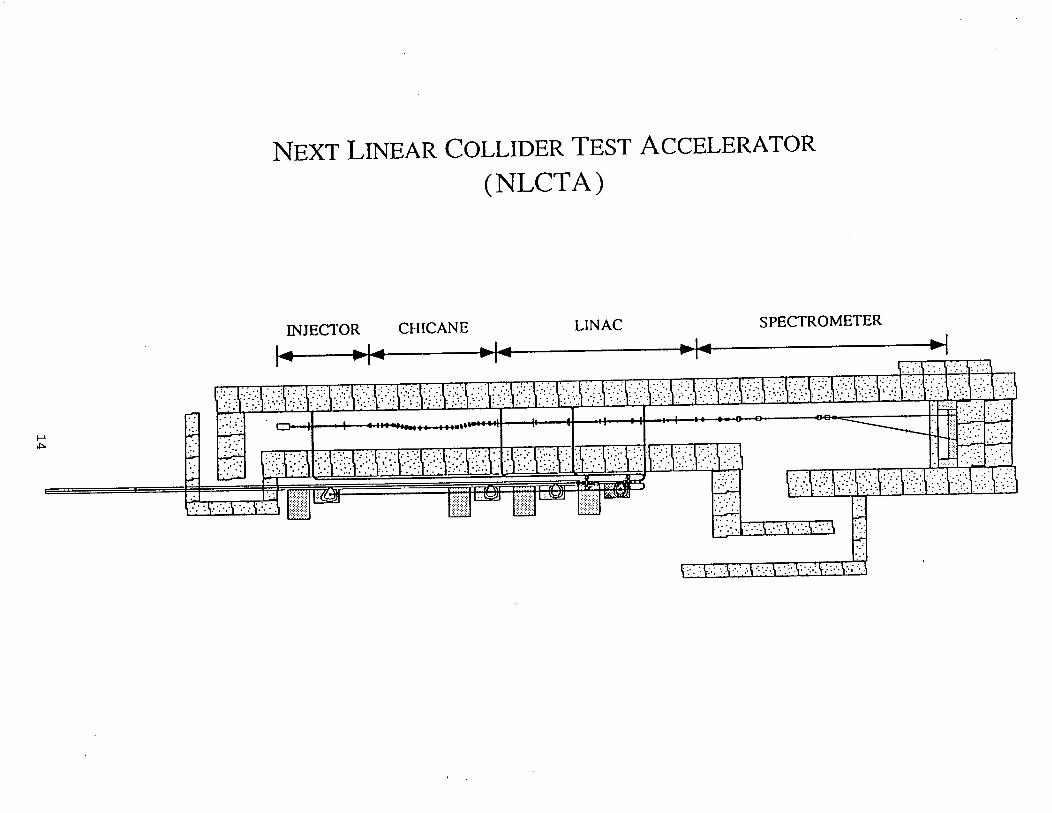
NEXT LINEAR COLLIDER TEST ACCELERATOR
(NLCTA)
~JECTOR CHICANE LINAC SPECTROMETER,
.,..
\“.\’ ~.~ .. ;. :..:.:..::.............,.... :.:..,’, .. . . ... ... .. ... , ,. .

NLCTA RF System
TEo1window It ++
I~----1
-:...
i
t.
<----’- :“.*
1
E:.\:.:,:........
L;?.:
.
t
\
, -.: --1\ ..-.
4
1
~
T’:::::::.~ti.........:.,...,
IT -k
7J
\ 11
+---- 1
‘> Dastis~dtiteupgrade
~ TEOI wave-guide valve
LegetiI
TE1~ m- ~~U.b TEO1 ctikr waveguide TE1 o / TEO1 Transducer
1-% ?wA3
15
-------- -. . . . . . . t

NLCTA RF System
Klystron
~Y
.,:::::::and .~:$jdriver ‘~
TEo1[window - +
r----I
s -:--.
%
... .
Pre-buncher Injector (2 x 0.9 m)cavities
11.4 GHz Distribution
r%-::$W::: ;::::; ,
●
f
,,?
... ........... ... 0I
T - L 7 ‘:41..J
F.,1
\/”\/I
t,----I8 - :“..
T,:,:,:,:,:.:,,.:.::,&~~ .,.;: (.....................
I
r----I
L-:..*
I
*
F:::::::::::::+?.......:...
I
t, ~.: --1u .. Dashes
indicate
1upgrade
\ --u TEO1 wave-
guide valve
SLED-II PulseCompressors(40-mlongdelay tines)
Linac(6x 1.8 m)
I
Legend
TE1o rectangularwaveguide TEO1circularwaveguide TE1o / TEO1Transducer
1-95 7880A3
16
,-—

Klystron Status
9f12/95
NLCTA Spec: 50 MW, 1.5 ~sec.
● 3 Klystrons operate at NLCTA Spec.
● XL2, XL3 - increased Band Width.
● XL4 to be completed this Fall.
● XL2, XL3, XL4 go to NLCTA.
● PPM Klystron detailed design inprogress.
17

Tek Run: 125MS/s *pkt ............- . . J
4+. ,.”- ---- 4
~~~ I Ch4 Fall13.6ns
Lowresolution
“1—
chi’ i~oo v’1
‘chi’ ‘5;oov: M “400ns ‘Ahx f‘ i.’o’l’v 3 May lggs
Ch3 1.00V Ch4 5~;oy:Q1.00 v 11:22:46
~zendCati& Voltige: 432 kVCati* Current: 337A
Collector Current witi ti on (0.8% intermptd current)Collmtor CWent witi K off
Klystron Output Power: 50 MW (Pin=631 W)
18

RF Pulse CompressionStatus -
9J12f95
NLCTA Spec: x6 compression200 MW x 250 ns out
● Prototype SLED II System Tested
● X6 190 MW x 150 nsec output
● x7 205 MW x 150 nsec output
● NLCTA production components:
● detailed design complete.
● SLED II delay lines machined, readyfor flanges
● RF Transport waveguide machined,ready for flanges
● Mist parts, mode converters, couplers,bends, tapers in production.
19

I I I I I I i I I I 1
200
160
g .120z
40
0
– – - Klystron
—SLED-II
L
III 1 I I I I [ I I t
lWns/div

I 1 I I 11 T
+ .. . . .. .. . . . . .. .. .. . . . . . . . . . .. . . .. . . . . . . .. . .. . .. . . . . . . . . .. :
. . . . .. . .. . .. . .. . . . . - ..-—--
---- .Q.—
-.....-.......-.....+_
_..........--—..+— —4 -
1 1 I I 1 I I 1 1 1 I 1 I a 1 1 i 1 I 1
0
“o
21

RF Structure Status
9/12/95
NLCTA Spec: 50 MV/m --> 85 MVlm1.8m Detuned or Damped Detuned Structure
“ First Structure:
● Asset Test ~7akefield O.K.
● High power Test --> 65 NIV/m (power limit)
● 400 additional Cells received
● 200 --> 2 injector structures.
● short stacks. couplers brazed .
● 200 --> KEK --> diamond point finish machining.
● Delivery expected mid September.
. Damped Detuned Structure (DDS)
● SLAC/KEK collaboration to construct 2 DDS structures.
● Detailed design in progress
● First cold test stack tested
● Remaining 4 cold test stacks due mid September
● Asset Test scheduled for 6/96
22

23
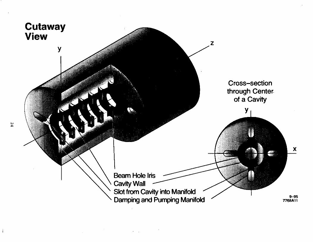
CutawayView
z/
Cross-sectionthroughCenter
of a Cavity
\
\ SlotfromCam intoMantiotiDampingad PumpingManifti ‘
x—

1
nmm
lx I I I t!
I I1. 1: I I
1
x
I
I
o 0 0 0 0 0 0 0 0* m N- 0 w m s m0 0 0 0 0 z 0 0 0 00 0 0 0 0 0 0 0 0 00 0 0 0 00 0 0 0 0
0 0 0 0 0 ~ 0 ? + ?
S3H2NI ‘SS3W9~S WOUj NOUWO
25
1

Modulator Status
9J12195
● 1 of 2 Power Supplies installed.
● First Modulator delivered to NLCTA.
● check out next two months.
● Remaining Modulators to be installedsequentially.
26

I
~odulator (B1umlein PFN, trans. ratio = 7:1)
PFN Voltage (hV)Rise/F~l Ener~ Efficiency (%)J?R + Thyratron Loss Efficiency (%)Net Energy Transfer Efficiency (%)
}CV2, 2 klystrons (J)Power Supply Efficiency (%)Net h!odulator Efficiency (%)
Thyratron Heater + Res. Pwr. (h\17)*Ave. AC input Po\ver (kll?)
(Excluding Aux. P\vr.)Pulse Conlpressioll
Type of P.C. SystemCompression RatiolntrinsicEficiency (%)
Loss Efficiency (Delay Lines,Hybrid and 2 F. P.’s) (%)
SLED-11 Eficiency (%)
SLED-11 Power GainPo\ver Trans. Eficiency (%))Net P. C. Efficiency.
Incl. P\\’r. Trans. Loss (%)Xet Po\ver Gain
Net RF Svstenl ParanletersTotal AC Po\ver. (~fl~~)
(Excluding Aux. P\vr.)RF System Efficiency (%)
(Excluding .4tlx. P\\’r.)Total Aux. Po\~er (1~11’)
Total AC Power., incl. Aux. (h~ll~)
. RF System Efficiency, incl. Aux. (%)Ave. Beam Power (Jll?))RF to Beam Efficiency (%)
500 GeV
TRC Design
65-
9i
77.5
93
&(1.5)50.0
SLED-11
5
SO.4 ‘-
96773.85g~
9s ..-
31
‘1.5
103308.4~,~
1 TeVUp~ade
688397803309576(1.5)41.7
SLED-II580.4
96773.8594
72 .
3.6
197
33
27

28
.,.-

Development and Advances in Conventional
High Power RF Systems %
Perry B. Wilson
SLAC
Presented at the 1995 Particle Accelerator Conference, Dall~, Texas
May 5, 1995
There now exists an International collaboration for R&D Toward
Ye V-Scale Electron-Positron Linear Collider~ . At EPAC’94, the
Councfl of the Collaboration appointed a =cal fiview Cm-
.mttee (TU >charged with preparing a report on the status of lin-
ear collider technology and the progress to be expected by further -
R&D over the next few years. The report is to be submitted to the
*Collaboration Council shortly after the LC’95 meeting (Tsukuba,
Japan, March 27-31, 1995). This talk is b~ed in large part on
material collected for Chapter?&(Linac Technology) of the TRC
report.
29

+
Compressor
Damping RingJ
t e-
Electron Source
‘i
\
Final /
Focus
\
Electron Source -
T \ e-
Positron Source
4
+ e+
Damping Ring\
Compressor
Main Linac
3eam Dump
r
) Detector
LBeam Dump
Main Linac
“LPre-Accelerator ~
Compressor7-qo 44*4A96
.,
30

31

. .
i
32.
.. .
. .
33

Table 2.3.1
General W D-i@ Parameter for Main Mnac
T~LA SBLC JLC NLC TBNLC VLEPP CLIC
~ f~uency (GHz) 1.3 3.0 11.4 11.4 11.4 14 ’30
Acmlerating GrdientUnld4/ti4 (MV/m) 25/25 21/17 73/53 50/37 100/74 -. 100/91 ._. –_80m
Active Linx Lengthi) (km)—-. . ..—
20 30.2 9.5 14.2 7.1 5.8 6.3%td Linx ~hY) (km) 29 33 10.3 15.6 7.8 7.0 9.4PeakPo= per Meter (MW/m) 0.206 12.2 100 50 200 lm 144.—-Structrtm*– - Utit ‘“ - 32 2 4’ 4 1 4 2StNCtUW.k@h p Pu (m) 33.2 12 5.2 7.2 1.8 4.0 0.56T@ Numberof - Uniti$) m 2517 lm 1970 3938 1400 11233T* Number of KI~trons 604 2517 — 1400 —
m 2517. ‘w’ 1970 26 140 2
10 50 150 180 120 m 2530/1210’”
m Pul= kgth atSt?.(ps) 1315 2.8 0.23 0.240 0.24*) 0.11 .0116, W % Cu-tC}(A) .m 0.30 O.m 0.74 1.49 SB SB/1.94
Total Ave.’RF Pm. ●t Str. (MW) 54 51.6 32.4 30.5 41 22 26.6,
4)
5)
6)
. .

. .. “e
j .
35
.

i
36
.

37... .

Klystron Parameter: Design Goals and Achieved to Date *
‘1#
I
RF ~uency (CHZ)Peak Output Power (MW)Pub hngth (pa)Repetition Rate (Hz)Ave. Output Power (kW)Microperveance
FElmtronic Eficieocy (%)wed Max. WCY2) (%)
Beam Voltage (kV)Beam Energy per Pulses) (J)Cathode Loading (A/cm2)CathAe HeaterPwr, (kW)Musing Tyw%lenoid Power (kW)Output Window Typ
No, of Windows/KlystronOverall h~h tm)
TESLA I SBLC
Daign
1.37.1
13141093
0.51)7073110
13,300
0.5sol.
4coax
1
Ach.’d
1.35.0
201010
2.04550130
10,100
sol.4
Pillbx
12.0
*
50211.2506257584061
PPM—’
Pink
2
‘2.5
60271.842535281070
62
sol.15+.
.
42.5
JLC
TM}gn Ach.’d
11.4 11.4135 96500.5 0.1/0.2150101.2 1.245 33
*150 170
~ 13.50.5 0.5
SCM sol.‘1 40+
TEII TEI1TW A/2
2 21.5 1.5
N1,C I VLEPP
l)mign
11.4501,2180110.66071
4551007.40.4
PPM—
T&l ~TW
11.3
AcII.’{I Design
11.4 14
5SIT2 ~ 150o.~/l.~ 0.50
60 3001/5 241.2 0.25
43/37 6062 76
400 1000125
7.6. 51.0
SOL PPM+R20 —
Tbl TEI 1Sw ‘ TW
1; 21.3 1.46
Ach.’d
10.72
0.154078
1000
51.0
PPbl—
TE1]
21.46

?F~
39... .

Scheme of tie ~PP RF s~tem ..
.
.
1’ \
\J,,~Q*K\i
P’
PT*9
41
.

2 3< ~ a !,!.
t—! ———-
-—. ..— ..~.
I
●
,.
: ..
.
42
,..

7RC-’~~ 203.~
Modulator Parametem: DesiUn Goals and Achieved to Date
TESLA SBLC JLC NLC VLEPP
Modulator Typel) Storage cap. PFN Blumlein PFN Blumlein PFL Gridded Gunwith bollncer
D-ign Ach.’d Hagn ,Ach.’d hign Ach.’d Deeign Ach.’ds) Deign Ach,’d
Flat Top Pul= Length, T~(ps) 1314 2010 2,8 3.0 0.5 0.7 1.2 1.5 0.50 0.50PFN Voltage (kV) 9 10 65 43 120 80 mu *95 1000 960fimformer Ratio n l:l& 1:13 1:18 1:23 1:7 1:7 1:20 — —Riu/Fdl Energy Eficiency (%) y ~6:’ ,; 70 80 =60SC~~ Energy EfiCienCy~) (%) 99 — 70 81 56 — —
IzR/Thy./Gm b ~ciacy (%) 97 95 97 97Wergy Stired on PFN3) (J) lm 1650 174 256
Power Supply Efficiency(%) 95 90 95 93 a90Mod. Eff. without Aux. P-r (%) 79.5 a60 a i2 a 52 95Auxiliuy Power4)(kW) 1.5 3 1.5 1.5 1.5 0.3Net Modula@r ~-y (%) 86 M 77.5 59 m 70Ave. AC Input Pm (kW) 155
92.5 554.2 a ’29 51.5 40.5
(Including Auxiliary Pomr)
\\
.

.
i
,
44
...-

I
Development And AdvancesIn
SLAC-PUB-95-6957June 1995
ConventionalHighPowerRFSystems*
P. B. WilsonSaford Linear Accelemtor Center, Smford Universi~, Stanford, CA 943W USA
The development of rf systems capable of producinghigh @ power @undreds of megawatts) at re~vely shortptdse lengths (0.1-5 micro=nds) is currentiy being drivenmainly by the requirements of future high energy tin-co~iders, although here may be applications to irtdustrid,mdd and reswch finacs as we~. The production of highpeak power rf typically involves four basic elements apower supply to convert ac from tie “wall plug” to dc; amodulator, or some sort of switching element, to producepul~ dc power; art rf source to convert the ptised dc topulsti rf powen and possibly art rf pulse compressionsystem to ftier enhance the peak rf power. Each elementin tiis rf chain born wdl plug to accelerating structure mustperform with high efficiency in a linw co~ider application,such tit tie ovefl system efficiency is 3070or more. Basicdesign concep~ are discussed for Mystrons, modulators mdrf ptdse compression systems, and tieir prwnt design statusis summarized for applications to propod Iinm coltiders.
I. I~RODU~ON
There now exists an lnlerlaborato~CollaborationforRU Toward TeV-Scale Electron-Positron Linear Colliders.The colhboration consists of some 23 member institutions inEurope, Asia and the United States with an interest in linearcollider development. The Council of the Collaboration(consisting of one representative from each memberinstitution) met at EPAC’94, and decided to appoint aT=hnicd Review Committ& ~C). This committ= wascharged with preparing a report on the present smtus ofhear colfider technology, and the further R&D nded overthe next few years to r~ch these design goals: an initialluminosity in excess of 1033cm-2s’1 at a center-of-massenergy of 500 GeV, with the capabihty of being expanded inenergy and luminosity to reach 1 TeV mnter-of-m=s energywith a luminosity of 10Mcm-k-l. A draft of tie report wtilbe submitted to the Collaboration Council in June, 1995.This paper is based in large part on material collected forChapter 3 @inac Tuhnology) of the TRC repon.
The major proposals for future linear colliders havebeen described in detail elsewhere (see for example thesurvey tis in [1]). TESLA ~eV Superconducting LinearAccelerator) is a proposal for a linear colhder based on tieuse of superconducting accelerating cavities at 1.3 GHz.The TESLA R&D program is an international colhborationof about a dozen laboratories, coordinate by the DESYkboratory in Hamburg, Germany. Use of a superconductingcavity avoids tie need for very high peak rf power. Such acavity is in essence an rf pulse compressor, storing energyover a relatively long time period (on the order of amilliswond) horn an RF pulse with a relatively low peakpower. An advantage of the low TESLA rf frequency is alarger beam cross-section and looser tolerances onconstruction and alignment. The SBLC (S-Band LinearCollider) is a proposal, dso based at DESY, for a linear
collider with an rf frequency of 3 GHz. B~ause of tierelatively low rf frequency, the SBLC also hascomparatively loose tolerances. A strong point of fiispropod is that it is supported by a wide base of existing S-band accelerator Mhnology, in particular the SLC prototypehear colfider at SLAC. The MC ~ext Linm CoMder)isa proposal by SLAC for a linear collider at 11.4 Gm,exactly four times the SLC frequency. The principaladvantage of a higher rf frequency is that a higheraccelerating gradient cart be obtaind for tie same ac inputpower, resulting in a shorter length and possibly lower costfor tie main linac. A major disadvantage is that tightertolerances are required for the consmction and digrtment ofthe accelerating sections and focusing magnets. Nso, higherpeak power is required from the rf sources, with aconsWuence that some form of rf pulse compression isnecessary. The KEK laboratory in Tsukuba, Japan, hasproposal tie JLC (Japan Lina Collider), dso at 11.4 GHz;it k quite similar to the NLC in its main d~ign parameters.VLEPP (standing for “Colliding Linear E1wtron-PositronBeams” in Russian) is a proposal for a linw mllider at 14GHz, which originated at the Institute of Nuclear Physics~) in Novosibirsk, Russia. The R&D for tie collider isactually taking place at Protvino, Russia, near Serpukhov(about 100 km souti of Moscow). It is being carried out bypersonnel from a Branch of the above institute (BINP).Unfortunately, tie monomic situation in present:day Russiais such that a full-sale VLEPP wfil probably not k fundti.However, a swong R&D program is still going forward atProtvino; his work will provide useful results which canex~ite tie otier collider programs. CLIC (CERN LinearColtider) is a propo~ for a two-km iina collider based .at CERN in Geneva, Switzerland. In the CLIC design (seepaper by K. Htibner in [1]), 350 MHz superconductingcavities are used to acmlerate a high-current drive beam to 3GeV. The drive beam consists of trains of bunches in whichthe spacing between bunches in each train is the rfwavelength at 30 GHz, These trains pass through a series oflow impedance “transfer structures”, where they induceabout 90 MW of peak rf power for a ptise duration of 12 ns.This power is then transfemti through waveguides (two formch transfer structure) to tie accelerating wtions in themain linac. The TBNLC ~wo-Beam NLC), proposed by a5oup at LBL and LLNL, is dso a two-beam acceleratorscheme, but in tiis case the drive beam is powered byinduction linac modules. The TBNLC is proposed as analternative power source for tie NC, in particuk as a high-gradient upgrade to 1 TeV. Instead, of a single drive beamper main tinac, as in the case of CLIC, tie TBNLC wouldconsist of 18 separate drive beam uniu for each of tie twomain linacs. There would be 150 transfer structures perdrive beam, mch supplying 360 N of power to a single 1.8m NLC accelerating section.
The various proposed colliders and their operatingfrequencies are listed in Table I, along with otier basic
* Work sup~rted by tie Department of Energy, contract DE-AC03-76SFO05 15.45
Presentd at the 16~ IEEE Particle Acceleration Conference @AC95) and InternationalConference on High Energy Accelerators, Dallas, Texas, May 1-5,1995

parameters to be discussed in the following sections. TheSLC is tisti for comparison.
Ml of the proposed lin- mflide designs are based onthe production and manipulation of RF power in thefrequency range 1.3-30 Gm. The rf system itself mustconvert power from the ac mains (wrdl plug) to rf power atthe input of the accelerating structure witi the greatestpossible efficiency. In gened, it is wier to attain a highacwlerating gradient at a higher rf @uency. Nature has,however, imposed a powerful limi~tion on the gradientachievable for routine operation of a copper acceleratingstructure --- the dark current capture threshold. Thisthreshold is given by
where L is the RF wavelength. The tieshold gradien~ forthe various co~iders are fisted in Table I, together with thedesign gradients for a 500 GeV machine. It is indeedpossible to exceed this threshold gradient by somermsonable factor; for example the SLC routinely operates30% above it with barely detectable dark current. However,the dark current beam power dissipation, and hence thedifficulty in processing a structure to a given gradient level,tends to kome worse exponentiy as the capture thresholdis exceeded by a still larger factor. In the case of asuperconducting structure, field emission wi~ nmessarily bereduced to a low level by sp=id cleaning and processing@hniques to avoid unacceptable power dissipation at lowtemperature. Perhaps these heroic cleaning and handingprocedures can be a&ptd to copper structures as we~. Butin any case, if operation is ptind at a gradient significartdyabove tie capture tieshold, dark current effects must becareftily studied in an appropriate test facihty (such as tieTESLA Test Facility under construction at DESY).
For a high frequency high gradient finw coltider with acopper accelerating structure, nature has unfortunatelyimposed another limitation on the rf system. The energystorti per unit length on the accelerating strucrure wi~ sderoughly as G* L*. If the gradient is set at some factor timesthe capture threshold gradient, then the stord energy perunit length remains roughly constant, independent offrequency. However, the time allowd for this energy to becollwted in the accelerating structure depends on the energydecrement time,
(2)
Thus the RF pulse length wfll rdso tend to We as 0-3~, andsince the stored energy per meter is roughly constant underthe above scaling assumption, the
Ppower requir~ per
meter will tend to scale as & . Unfortunately, themaximum output power avaihble from a klystron tends todecrease rather than increase as frequency increase.Therefore high frequency RF systems using klystrons to
generate the RF power NC, JLC, ~EPP) ~uire somesort of pdse compression to enhance tie peak power outpu~However, the additional loss associated with themmprmsion procms tends to lower the ovd efficiency ofthe RF system. The two-beam accelerator conwpt ~NLC,CLIC) bypasses the limitations imposed by conventionrdMystrons in producing high frquency, high @ power atshort pulse lengths. The drive beam in a two-beamaccelerator is, in fact, equivalent to the - in a Uystron,and the TBA scheme is dso dlti a ‘hlativistic Mystron.”A co~ider using a superconducting accelerating structure~SLA) incr-s tie WO limitation on energy collectiontime by a hge factor over that of copper, allowing a longpulse, low peak power, efficient RF system. (A will betiscussed later, a long pulse modulator tends to be moreefficient tian one which must produce short, very high@power pulses). However, tiis gain in tie efficiency of RFpower generation is offset to a large extent by the additiondpower requirti by the refrigeration system.
Energy decrement times and peak RF powerrequirements for the collider designs are listed in Table I.For machines with copper structures, the structure fillingtimes (except for CLIC) are quite close to the values givenfOr~d; tie ~ pUIWleng&S ~ t~iCdly XVerd hmeS 10nger@ allow for acceleration of a bunch train. The pulse lengthsat the accelerating structure (in nanoseconds) are: SBLC(XOO); JLC (230); MC (240);VLEPP(110); CLIC (12). Inthe case of TESLA, the pulse length (1.3 ms) is rducedbelow the dmement time approximately by the ratio of therefrigeration power rquired per Watt of power dissipated at4.2°K (= 300). The @ powers do not scale as ~~ asdiscussed above,-use theactualdesigngradientsdonotcloselyfollow a G ~ scaling, However, as smn in Table I,the peak power per meter does increase rapidly withincreming frequency. Likewise, the linac length would beroughly proportional to A for G - G ti scaling. The actualdesign lengths do show a strong correlation with frequency.Since the stored energy per meter remains approximatelyconsmt for G - Gth scaling, ~he average AC wall-plugpower should scale roughly as PAc - frk / TY, where fr iSthe repetition rate and ~ is the RF system efficiency. Asfrequency increases, the colliders in Table I made at leastpart of their wavelength advantage for a higher repetitionrate. These rates are (in ~): TESLA (10); SBLC (50); JLC(150); NLC (180); UPP (300).
A. KlysPons
At a constant beam voltage, the RF output of a Hystron(or other microwave power source) increases as the beamcurrent incr=ses. However, a higher - current, Ib, at agiven beam voltage, Vb, inevimbly lead to a lower efficiency .kcause of the detrimenml effects of space charge forces.These forces tend to blow apart the sharply defined bunchesneeded for high output efficiency. The micrope~wce(defined by KL = ]b~b3i2 x106) is commonly tien as ameasure of these space charge effects. If klystronefficiencies, obtained from both measurd prforrnance and
46

sim~ons, are plotti as a function of microperveartm, it isfound that the collection of mints (see for example [2], Fig.3) is quitesharplyboundti by the l~e -
quy = 0.80 -0.15KP . (2)
bw frWuency, long pulse or CW Uysmons tend to fdlcloser to this performmce limit than high frquency, high@ POw~ tu~s. me intercept at zero perveance has Wmetieoreticd justilcation. A 100% efficiency implies that Mthe elwtrons in the b are just brought to rest by the RFvoluge of the output circuit. This is not possible in a r~Mysnn tiuse there is an energy sprwd in tie - due tothe bunching process, and because the RF voltage vtieswith radius across the gap. Also, even a single elmtroncannot be stopped in a gri~ess gap; art elecmon on axis mk at most about 85% of its energy [3].
There is also the perennial question concerningImitations on @ Mysmon output power as a function offrequency. This cart be rougNy estimated as fo~ows. FirsLthe beam radius is limited to something like W8 to dow forreasonable gap coupling. Saond, the current density perunit area from the cathode (cathode loading, Id is limited toabut 10 ~cm 2 for good cathode lifetime. Third, the areacompression ratio, CA, of the kam in the gun region istimited by optics and tolerances to perhaps 150. Puttingtiese factors”togetier gives
P mm ~ ~Vb[IACAn(k / 8)2] = 74qVb(k / C~)2 (3)
where q is tie electronic efficiency. If the tube is to beefficient, and if we apply Eq. (2) conservatively, *en themicroperveance for an efficiency of 50-6070 is limited to
Usin Eq. (2) together with6 ~12
$[ ~;(Kp x1O )Vb . we find that for Vb= 500 kV themaximum output power is shut 100MW up to 14 Gm, henMs off as k2 above this frequency.
Table 11lists klystron parameters for the five colliderpropo~s that use Mystrons as an RF source. Both designparameters and values actually achieved m date are shown.The numbers given for “scaled maximum efficiency” areobtained from Eq. (2). Note that tie design values forefficiency are dl we~ below time mmimum values, exceptfor the law fiwuency, long pulse TESLA Mystron wheregood efficiency shodd be r~atively *SY to achieve. Two ofthe Mystrons have achieved the design p~ power. TheSBLC S-band klystron, designed in collaboration withSLAC, has reachd 150 MW at a 2.8 w pulse length [4].The NLC X-band Uystron has achieved 50 ~ at 1.5 KS[5]. Both klystrons still fdl short in efficiency, and bothmust eventually replace power-consuming solenoids withPPM (periodic permanent magnet) focusing orsuperconducting solenoids.
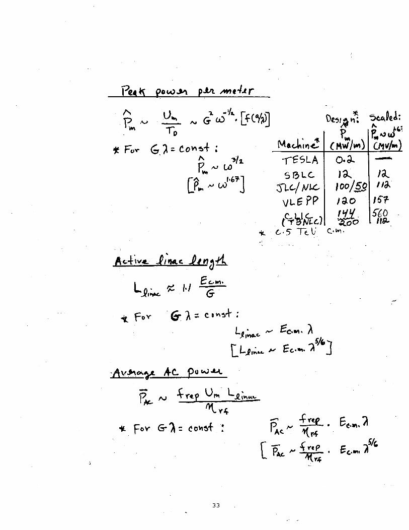
B. Modulators
The rise time of a modulator pulse is an. importantparameter in determining the modulator efficiency. In aconventional modulator, the pulse forming network GWcapacitance is charged by a DC power supply to a voltage
Vp~. This network can be eitier a length of smoothtransmission line, or a series of discrete capacitors andinductors which model such a line. The line is hendischargd by a switching device, usually a thyratron,through the primary of a pulse transformer with a turns ration. The output of the pulse transformer produces a voltagenVp~ @ (single stage PFN), or nVp FN (two stage, orBlumlein Pm. b the we of the TESLA modulator, anenergy storage capacitor is partially dischargd through theprimary of the puke transformer. The switching is done bysolid state devices (thyristors). A ‘%ourtcer” circuit is usedto compensate for voltage droop.
The energy efficiency, qE, of the pulse transformerisdefined as the useful energy in tie flat-top pordon of thepuk dividd by the toti energy in the pulse. The energy inthe fd-time portion of the pulse tends to s~e in proportionto tie rise time, TR, so that the energy efficiency can bewritten as q E = T~E = TK/~K + aT~, where TK is tieusefti tit-top pulse width, TE is the energy width, and a k acoefficient between 1.0 and 1.2 which depen~ on the pulseshape and tie definition of rise time. In turn, a sim le
?physical argument [6] leads to the scaling TR- nTE ~.Combind with the preceding relation, tiis gives
(4)
where ~ is a constant that can be obtained by fitting toexisting pulse Uansformer designs. For the pulsetransformer driving the 5045 SLAC Mystrons, ~ = 0.033@)l~. It is found that tie above expression then gives agd fit to a number of other puke transformers measured atSLAC having a variety of turns ratios and pulse lengths.Using Eq. (4), the energy efficiency is plotted in Fig. 1.
1.0 I I I I 11111 i I I I IIrr
0.8 –u n=5
~
:Z 0.6a
g
& 0.4
0.2 –9 t 9 ;
o I I I I 11111 I I 1 1 1111
0.1 1 10-?@l Al Pulse Length TK (w)
Figure 1- Energy Efficiency for a typical pulse transformeras a function of pulse length and turns ration n.
Mong with TK and n, values of qE from Eq. (4) arelisted b Table 111(as the scaled energy efficiency) for tie
47

!
rnodtdator designs for the various collider propods. Anaccuratedctdatin of energy efficiency must ~so includetie effwt of the load (klystron) capacitance, the seriesinductanceof the thyratron,msformer core losses, and theinductances of the cables and leads connecting thecomponenu. Of course, the best efficiency is obtained byefitig ti modtdator entily by using a Hystron with a- gum stitch the beam, as propo@ for WP.
C. W P&e Co~restion~ p* compression is a method of enhancing Mystron
ou~ power at the expense of puke width. Mthough someenergy is lost in tie compression process, tie efficiency canin principle be quite high. HighQ energy storage elementsare @uired to achieve efficient pulse compression; thesecan he ei- resonant cavities or lengtis of shorted delaytie.
RF @se compression is uti in thrw of the 500 GeVcollider designs. VLEPP and NLC use a SLED-type scheme(SBLC pbs to use a SLED system in a 1 TeV upgrade). Ina SLED pfie compression system [7], energy btids up in astorage demerit (resonant ~vity or resonant delay line) overtie major part of the Mystron output pulse. During the fitipart of the pfie, ~ual to the desird output puke length, aphase reveal at the klystron input triggers a discharge ofthis stored energy, which then adds to the energy comingdir=dy from the Mystron. During the filling time of tiestorage device,. there is an unavoidable power reflwtion; inaddition, some energy is left behind in the storage element.Together, these factors lead to a maximum intrinsicefficiency for a SLED system on the order of 80%, evenassuming Iossless components. Taking losses into accounttiuces the efficiency to approximately 75%. On tie otherhan~ the JLC uses a compression method, the Delay LineDistribution System (DLDS), which is inherendy 100%efficien~ Mthough rekted to Binary Pdse Compression [8],the DLDS system uses less delay line pipe by feeding powerin the upstream beam direction, thus taking advantage of tiebeam transit time to achieve a factor of two reduction in therqti deky line length. Both the DLDS and the SLED-IIcompression systems have tie advanmge or producing a flatoutput puke. This is a nwessity for accelerating long bunchtrains (tie h pulse length is about 120 ns for JLC andNL~. The VLEPP compression system is based on tie useof a single mvehg-wave “open” cavity resonator of uniquedesign [9], and is therefore very compact. Although theoutput puke is not inherendy fla~ this is of no consequencefor the acceleration of a single bunch, as is tie case forWP. Parameters for tie k pulse compression systemsare given in Table IV.
The overall RF system efficiency is an importantparameter for a bn= colfider. The AC power requiremen~(see Table I) for the various collider proposals range from60-150 MW. Thus a 1% improvement in efficiency canreduce the AC power consumption by a megawatt Or more.The net system efficiency, shown in the kst column in TableI, is the product of the separate efficiencies of the Mystron,
modtdator, and ptdse compression systems. If there is nocompression system, tie efficiency for transmitting powerfrom the klystron to the accelerating structure must beincludd instead. The system efficiency cart be cdctdatedwith and without auxiliary pwer. This includes power fortie Uystron catiode heater, Mystron focusing solenoid,thyratron cathode and reservoir heaters, md power for thecryogenic systems in TESLA and CLIC (which usessuperconducting cavities to accelerate the drive beam). Thenet RF system efficiency is, on the avemge, about one-third.
It is obviously highly desirable to increase the net RFsystem efficiency. For example, one can think ofeliminating the pdse compression system and the lossesassociatd with it. However, more dc pulse compressionmust then be ~ti out in the modtdator (or in the inductiontinac modules in the case of the TBNC). As anotherexample, a better Uysmon efficiency can be obtained byraising the - voltage and lowering the pervww. Again,this implies a lower modulator efficiency bwause a pulsetransformer with a larger turns ratio will be requird (or ahigher Vp~ could be used, which is more expensive andtechnically difficult). There are losses and inefficiencies ineach stage of the power handling and processing chainbetw=n the AC wall plug and RF at tie input to theaccelerating structure, Care must be taken that an efficiencyimprovement at one step in this chain is not made at tieexpense of incrases loss at another singe.
A long-range ex~ctation for the efficiency of tie RFsystem for a linear colhder might be on tie order of 50~0.This efficiency could be attained by a low pervmce, highefficiency klystron (65%) with grid switching (9570efficient), and a high-gain Binary Pulse Compression system(81% efficient including power manumission). The BPCsystem would use 10 or so discrete cavities per stage toeliminate long deky fines.
V. AC~OWEDGME~
The principal results on the status and development ofhigh power RF systems, as reported here, are containti inTables I through IV. These tables are the result of hard workover many months by members of tie Linac Tahnologyworking group of the Technical Review Committeementioned in the Introduction. In particular D. Proch~SLA), N. Holtimp (SBLC), T. Higo and H. Mizuno(JLC), N. SolyA ~LEPP), G. Westenskow ~BNLC) and I.Wilson (CLIC) were responsible for the major pordon of thiseffo~ with substanti input from A. Garnp on the TESLA rfsystem.
1. See survey papers on linear colhders by N. Holtkamp @.770), G. LWW (p. 777), V. E. Bdakin (p. 784), K.Htibner (p. 791), M. Tigner ~. 798) in: HEACC’92,Inst. J. Mod. Phys. A (Proc. Suppl.) 2B (WorldScientific, Singapore, 1993).
2, R, B, Palmer, W. B. Herrmannsfeldt and K. R. Eppley,“An Immersed Field Cluster Wystron”, SLAC-P~-5026 (1989).
48

3.
4.
Z. D. Farkas and P. B. Wilson, “Dynamics of anEl-n in an RF Gap”, SLAC-P~4898 Rev. (1989).U. Becker et al., “Comparison of CONDOR, FCI and 7.~ Cdcuhtions for a 150 MW S-Band Wysmonwith Measurement”; paper WAE13, these pr@ings. 8.E. Wright er al., “Design of a 50 W X-BandMysmn”, SLAC-PUB~76 (1999. 9.P. B. Wilson, “Applicadon of High Power MicrowaveSources to TeV Linw Colliders”, in Applications ofHigh-Power Microw@es, A. Gaponov-Grekhov and V.
GranaBtein, eds. (-h House, Boston, 1994), Sm.7.4.2..For a brief description of SLED and SLED-II withadditiod references, see [6], SW. 7.4.3.Z. D. Farkas, ~EE. Trans. Microwave Thary andT&hniques MTT-34, 1036 (1986).V. E. Bdakin and I. V. Syrachev, Proc. 3rd Euro-Part. Accel. Conf. @ditions Frontiers, Gif-sur-Yvette,France, 1992), p. 1173.
Table I Basic Parameters for Proposed Linear Colliders Designs at 5M GeVCoUder Type(l) RF Freq G~ * Gradient (2) -merit P* Power Active AC RF SystemPropod q. (1) Time u per meter ~ngti(3) Power(4) Efficiency(5)
(Gm) Wh)
TESLA SCA 1.3 7 25D5 0.6x10⁹ 0.21 20 154 35/58
SLC Q 2.856 15 2021 730 12 2,8 24 13.6/14.5SBLC a 3.0 16 1721 720 12 30 139 37B8
Cu 11.4 61 53n3 95 100 10 114 3omCu 11.4 61 37/50 98 50 14 103 30D1
VLEPP Cu 14 75 91/100 68 120 6 57 39/40
TBNLC TBA 11.4 61 74/100 98 200 7 106 39/40~IC TBA 30 160 78R0 22 144 6 100 26D5
(1) SCA = superconducting accelerating structurq Cu = copper accelerating structure; TBA = two-beam accelerator (withcopper main linac structure).
~ Design gradient wiwwithout -1A• loading @unch on crest).(3) tiludes overhud for BNS bping and energy management (see text).(4) AC power required for producing main linac ~, includes cryogenic and auxdiary power (s= text).(~ Efficiencies are given with/without cryogenic and auxfliary power included.
-
RF Frequency (Gm)Peak Output Pwr. (MW)Mse kgti @)Repetion Rate (=)Ave. Output Pwr. @~MicropervmceEktronic Effic. (%)Soled Max. Effic. 2, (%)Beam Voltage @V)B- Energymlse3) (~
Ctiode Load(Mcm 2,Cathode Heat Pwr. @wFocusing TypeSolenoid Power @~Ou@ut Window Type
Ie II KlystronTE:
-1.37.113141093
0.5 1)
70
73
11013,300
3.10.5sol.4
“coax
1
.AAch.’d
1.35.0
201010
2.045
50130
10,100
sol.4
12.0
arameters: DSI
w3.01502.8
50
21
1.2
50
62
575
840
61
PPM—
Wbox
22.5
c
Ach;d
T150360271.84253
5281070
62
sol.15
Mbox
4
2.5
ign Goals andn
-11.41350.5150101.24562
60015013,50.5
SCM1
TEll
m2
1.5
.
.
Ach.’d
11.4%/50o.lm.2
1.2
3362
620170
13.5
0.5sol.40
TEll
w2
1.5
~chieved to DaN
u11.4501.218011
0.66071
4551007.40.4
PPM
mlTw
11.3
“
.
Ach.’d
11.458/520.21.5
601/51.2
43n762
400
7.6.
sol.=20
mlw
11.3
>
n
m14
1500.50300
24
025
6076
1000
125
51.0
PPM—
TEll
m2
1.46
Ach.’d
14600.72
0.154078
1000
51.0
PPM—
TEll .
2
= 1.46
(1) Perveance per beam ti multibeam Hysuon. (2) q(Max) = 0.80-0.15 x Microperveance. (3) In flat-top p=pdse.
49

?vedto Date
BlumleinPm
Table~. Mo ]Iator PararrTESLA
Storage cap.with bouncer
ksi~ Ach;d
1314 20109 10
1:13 1:13
99 –
86 86155
ters: DesiwSBLC
Pm
oals and Act
Blumlein Pm
VLEPP
Griddd Gun~
Ach:d
0.50960—
—
hsi~
0.51201:5
897997
174
95821.5
8029
M
G0.501000—
—
95
0.392.540.5
%sifl
2.865
1:18
86.570
971000
9579.51.5
77.5542
G3.043
1:23
=6565
95
M5090
=6035988
=
0.7
801:7
70
70
m1.54001:20=6058
=90= 521.5
ksi~
124551:7808197
25893721.570
51.5
~ Top Pdse Length, Tk @)Pm Voltage cwTransformer Ratio nRise~d Energy Effic (%)Soled Energy Efflc.2) (%)12~yJCore bss Effic. (%)Energy Stored on P~3) (0Power Supply Efficiency (%)Md Eff. without Aux. Power (%)Adiary Powd) @~
Net Modulator Efficiency (%)Ave. AC Input Power (kW)(Including Auxiliw Power)
(1) Pm= Ium@ element pulse 1(2) see texL
ming network Pm = ptie formingfine(Eansmissiontine).
(3) Energy switched per pulse from storage element for TESLA and VLEPP.(4) Includes thyratron cathode heater and reservoir heater power.(~ With stan~d (not Blumlein) P~.(@ Uses a Pm as energy storage elemen~
Power TransmissiTable IV. RF Pulse Compression ant n: Design and Act eved to DateVL
SLED.NLc
mAch.’d
4.55500/110
723.3953.1
150
DL
Design
25oon50
981.%95
1.8693
5.24524282
)s
Ach,’d
)-n
Ach.’d
6
Type of Pulse Comp. System 1, SLI
=5 4.55
500/1 1074
3.3795
3.2070
4.00480
2502x75
Compression RatioInputiOutput Pulse ~ngth (ns)Compression Efficiency (%)Power GainPower Transmission Efficiency (%)2)Power Gain Including Trmsmission LossNet Efficiency hcluding Trans. Loss (%)Ungth of Structme per Power Unit (m)3)Power at Structure per Power Unit (wMaximum Power in P.C, SysEm w)
1200240
76.5
3.83
94
3.60
72
7.20
360
380
900/150733.7843.0
150205
Rwuired Wysuon Power m 2x50
DLDS = Delay Line Distribution System; Wh = WEPP Power Multiplier.The power transmission efficiency in percent for TESLA, SBLC, TBNLC and CLIC are, re~tively, 96,97,98, md 90.
2 x 141
(1)(2)(3) A power unit is: TESLA, one klystron with modulator fding thirty-two 1.04 m acmlerating sections; SBLC, one
Mystron with modulator feeding two 6.0 m swtions; LC, two klystrons with two modulators driving one pulsecompression unit which f-s four 1.31 m s~tions; NLC, one modulator driving two Uystrons which mgether drive onepulse compression unit fting four 1.8 m sections; TBNLC, one Eansfer sncture for each 1.8 m wtion; VLEPP, onegrid-modulated Hysuon driving two WM cavities which togetier f=d four 1.0 m wtions; CLIC, one transfer smcturedriving NO 0.28 m sections. The toti number of power units (2 linacs) are: ~SLA, 604; SBLC, 25 17; LC, 1804;NLC, 1968; TBNLC, 3938; VLEPP, 14W, CLIC, 11233.
50

SMC - NLC
xsL
● DESY
MODULATOR - POWER SUPPLYPARAMETER SPACE FOR FUTURE
LINEAR COLLIDERSGEORGE CARYOTAKIS
\
51
S - Expanded SLCL - Superconducting Cavities - Tesla
MODUWTION
Diode - Line typeGrid -Switch Tube
● REQUIREMENTS FOR 1 TEV+
..
,.. _.
- .-
I
- -*B----- -k r 4-
‘-\...Pui —.
FIG 2. Beam prepar~l]on system
52


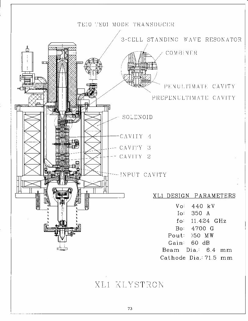
TE1O-TEO1Mode Transducer
/3-Cell StandingWave
A / ResonatorCombiner
PenultimateCavity‘PrepenultimateCavity
Solenoid
Cavity 4Cavity 3Cavity 2
InputCavity
1’1 HII
%’I
N
.4
\
n
r
1
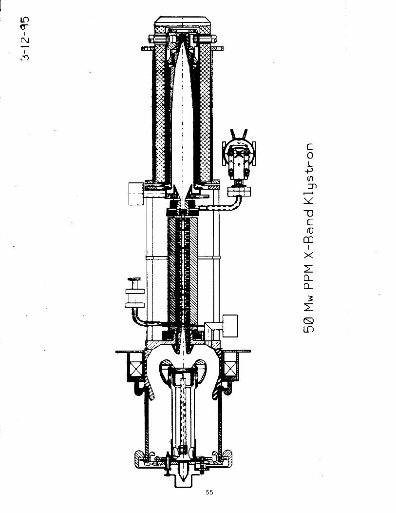
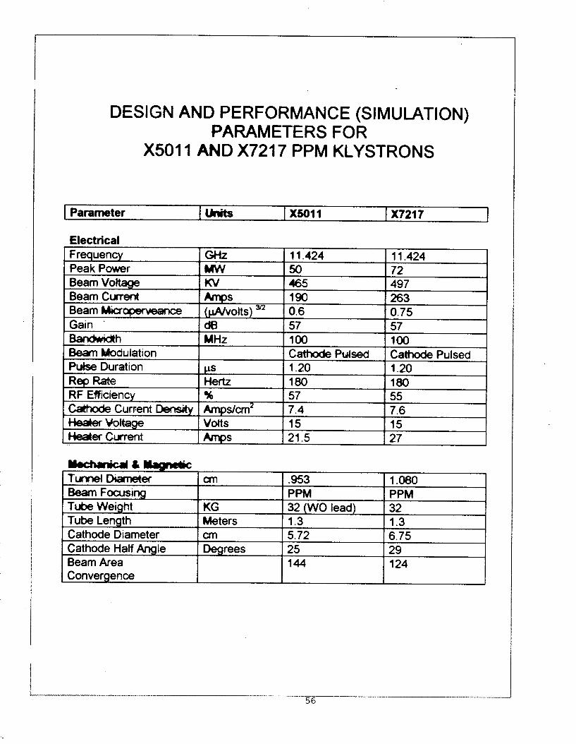
DESIGN AND PERFORMANCE (SIMULATION)PARAMETERS FOR
X501 1 ~D X7217 PPM KLYSTRONS
ElectricalFrequency 11.424 11.424Peak Powr 50 72Beam VoRage KV 465 497Beam Cwent -s lW 263Beam ~~~ (@ volts) = 0.6 0.75Gain ~ m 57 57~h MHz 100 7100Beam Wdulation c- Pulsed Catiode Pulsed- Duration P 1.20 1.20R~ Rate ;* 160 ] lmRF Eficiency % 57 55~ Current - *dmz 7.4 7.6& Voltage Vtis 15 15-er Current -s 21.5 27
1 9 lV1
T- Weight KG 32 (WO lead)Tu& Length Meters 1.3Cathode Diameter m 5.72Cathode Half ~le Degrees 25Beam Mea 144
I Convergent I
.“
rrr d
321.36.7529124
I
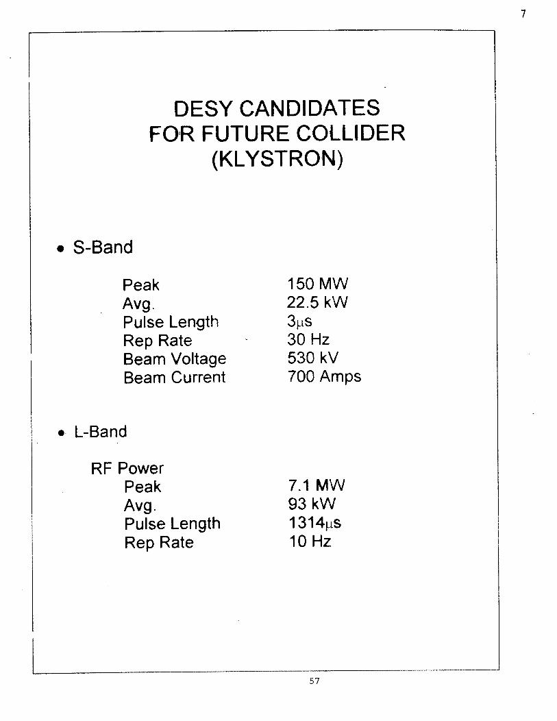
DESY CANDIDATESFOR FUTURE COLLIDER
(KLYSTRON)
. S-Band
PeakAvg.Pulse LengthRep Rate ~Beam VoltageBeam Current
. L-Band
RF PowerPeakAvg.Pulse LengthRep Rate
A50 Mw22.5 k~3~ls30 Hz530 kV700 Amps
7.1 MW93 kW1314psIOHZ
7
57

58

I —“=1
“>
-:
= &_-< ,.f
59

Existing and simulated high power S-band Mystron designs
Parameter
Bem voltage
Bem current
Pin
Poutmo Efficiency
SaturatedGain
Tubebngth
Tube and Maqet Wei@t:
Cavities
DESY ~yShOR
~easurewnti)
527
670
0.62
155
44
54
104
5000
7
Fropoged Mystion(Simulation)
600
669
156
203
50.6
31
80
400
4
kv
A
kw
MW
‘/0
dB
inchm
lbs
Fig. 4

— .—-.
!
1
I
I
t
,<-
C—
-e-, -
w‘.w
1
**“,,
t n,, ~,, n,
111 \
n—7
a
mm
I 1 _.—

CONVENTIONAL KLYSTRONBEAM MODULATION MODES
FREQ DIODE GRID SWITCH TUBEx d ? d
s d d d
62
13
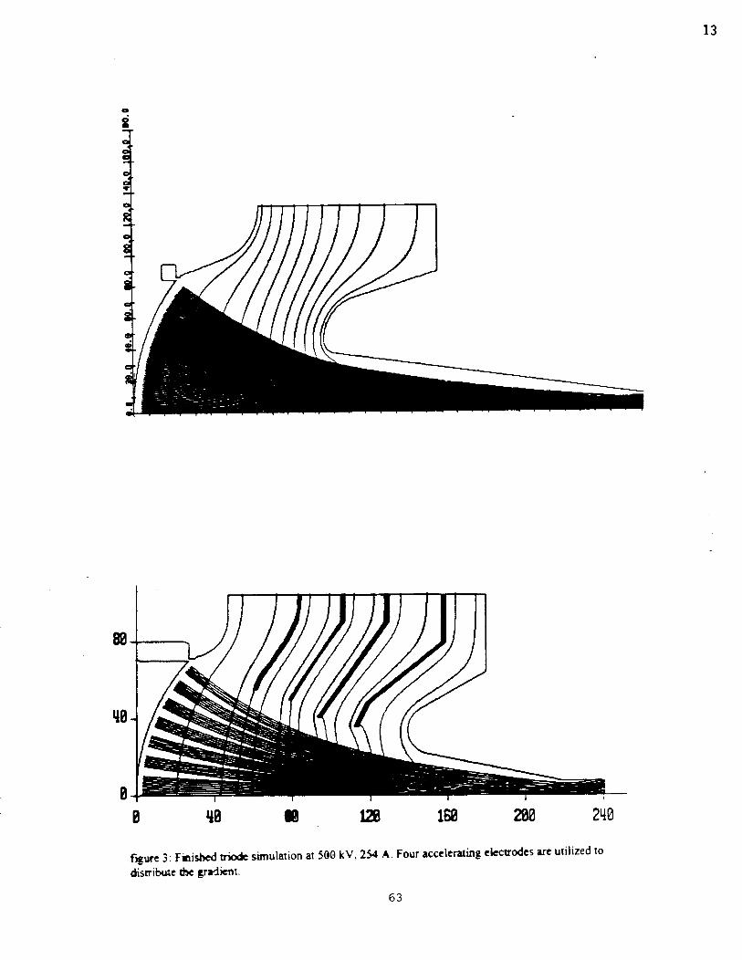
f~tie 3: FrniW - stimulation at 500 kV, 2M A. Four accelemhg el~udes we utilized to&swihte h ~titit.
63
I
..
.
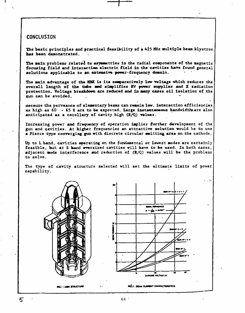
CONCLUSION
~e basic principles and practical fuibili~of a42S~mltiple be-klystrok been demonstrated. .
me main problems relatti~ to ~tries in the radial coqonents of tie magnetifocuing field md bteractim ●lectric field b the ctities have found generasolutions ●pplicable to an =Cemsive pr-frepncy -in. . .
fie main ●dvantage of the - is its qaratively low voltage which reduces th,werdl length of tbe * d 8411fies W powu supplies and X radiatiolprotection. Voltage bre~ ue rhed and b q c8ses oil isolation of thl~ can be 8voided. .
.-came the pemeance of ●l-ntary be- can r-in low, interaction ef f icienc ie!as high as 60 - 65 Z ue to be e~ected. Wge ti~tameous bandwidfi are als<anticipated u ● coroll~ of utity high (RN) values.
Increasing power and f~~ncy of operation -lies futher development of thfgun and Cavities. At Mgbe r fre~enc ies ● n attractive solution would be to US(a Pierce ~ comrgimg P with discrete circular -ittimg uea on the cathode.
@ to L kd, cavities ~ratimg on the fundamental or lowest =odes are ctrtainl~feasible, but at S kd e-rsized cavities will have to be used. In both cases,8djacent b interference - reduction of (R/Q) values till be the problem:to solve.
fie we of caviv st-ture selected will set the ultimate limits of powezcapability.
-. ..
5 64

14
BEAM-VOLTAGE PARAMETERRANGE FOR 200 MW KLYSTRON
Vo 10 S(KPERV) No of Beams200 2000 22.4 20300 1333 8s1 10400 1000 3.95 5/1 o500 800 2.26 4600 667 1.43 2
65——_..

NLC KLYSTRONREQUIREMENTS
2 GEV
m
(Positron Booster Linac)
Peak power/pulse
No. Required
● 28 GEV (Various)
length
Peak power/pulse length
No. Required
150
. 500/1000 GEV (Main Linac)
mPeak power/pulse length
No. Required
L—
MWI1O@ or 250
12
s—150 MW13.5ps
150
X(1 1.424)
50-75MWI1 .2ps
4,000-10,000

1
X3069-1 LINEAR BEAM TETRODE SWITCH TUBE

~ -. .__.—. --- —..,--
.-. .
●
.
e
1 1 I
...
. ..

EvaluateX-band PPM W MW md 75 MW klystrons.Build several pti-.
Do paperdesignof L-band md S-band ps MBK’s.Consider MB switchtubes.
Look atpossibili~ of a ~idded S-band ~K, althoughtibes tm few fm *riOus eff~ciency concerns.
If there is rnter- md tie numbers look promising,mnsider a 1&beam, 2W MW X-band MBK, (shortPU1*, no pul= compre=ion)withaseries ~ switchrobe.
Design for manufacturhg

I
70

●
●
●
~YSTRON SESSION SUMMARY
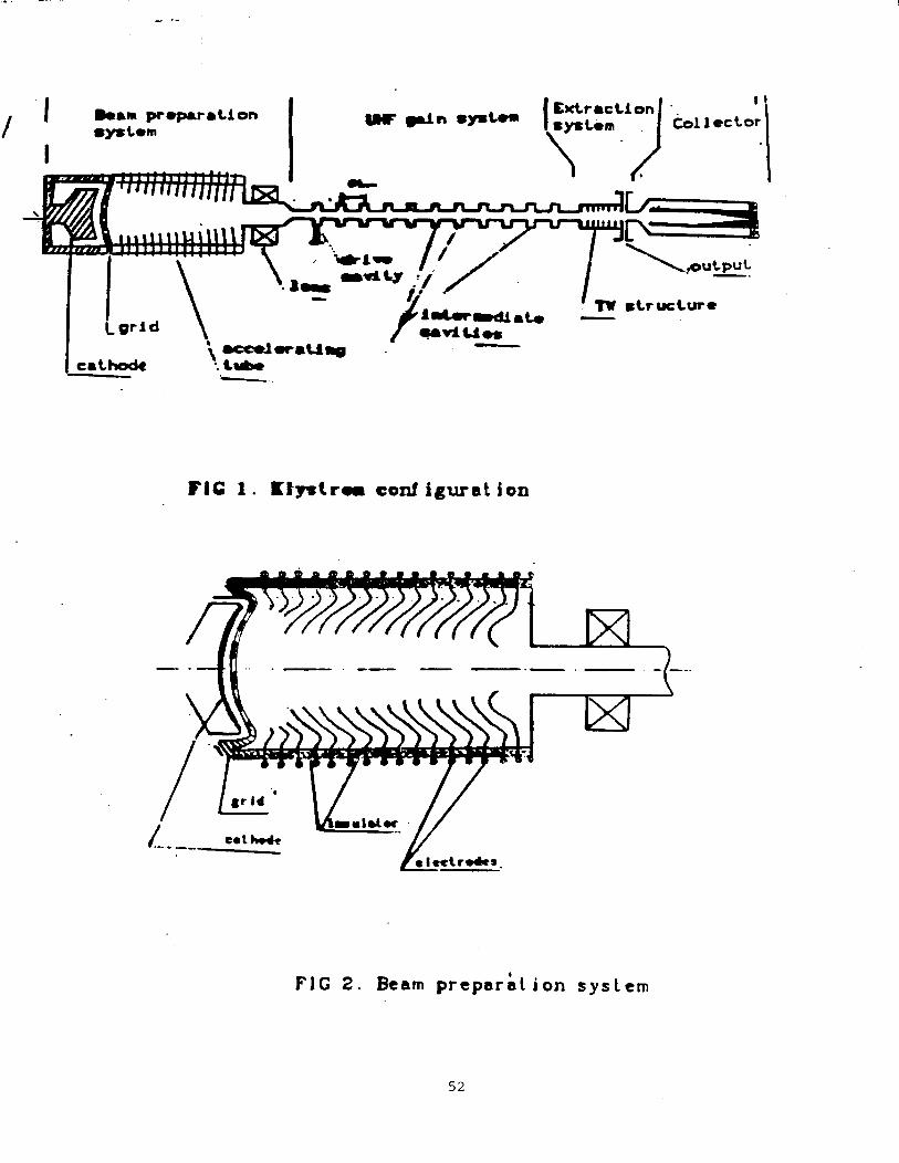
S. GOLD
PRESENT NLCTA USES 50MW KLYSTRONS,440KV @ uk=l.2
NLC PLAN (X-BAND)
50MW PPM KLYSTRONS, 465KV @ uk=O.61.5US
UPGRADE , 72MW PPM KLYSTRONS,497KV @ uk=O.75
S-BAND (DESY & NLC)
● 150MW, 535KV @ uk=l.8 , 3uS
Q UPGRADE , 200MW PPM, 600KV @ uk=l.4
‘,

1. What type of a load does klystron present to the modulator? Resistance, Capacitance,Maximum voltage, Rise Time.
2, What does the Mystron expect from the modulator? Would like and ideal pulse shape ofvoltage.
3. Since it appears one modulator will be used to drive two Uystrons, what will the load look liketo the modulator should one Mystron fail and what action should the modulator take? Theimpedance will double if one modulator fails. The consenses is that the modulator should faultand go off-line until the klystron is replaced.
4. How should a new klystron be processed? begin with a narrow pulse width at a low duty andslowly increase the width until the design width is obtained. Slow increase the duty until the designdu~ is reached.
5. As the tube ages the beam current will decrease at a fixed filament current due to the change inperveance of the tube. Therefore the need to adjust the filament voltage to maintain the beamcurrent w= discussed. No conclusion ww reached.
6. Maximum beam voltage ripple to maintain phase modulation was discussed. A chart tomaintain a maximum of 10° phase ripple is enclosed.
72
TE10-TEOl MODE TRANSDUCER
//
T
/ 1 \ /
3-CELL STANDING ~iVAVE RESONATOR/
/
/\
PE
‘ PENULTIMATE
/E PEN ULTIhl ATE
CAVITY
CAVITY
so~E~oID
CAVITY 4
CAVITY 3
—c AVITY 2
PUT CAVITY
XL1 DESIGN PARA
Vo: 440 k
METERS
v
Io: 350 A
fo: 11.424 GHz
Bo: 4700 G
Pout: )50 MW
Gain: 60 dB,,:LJn
Beam Dia.: 6.4 mm
Cathode Dia.: T1.5 mm
73

—
L ;?
---
—-——
74

l,YSTRON PROCESSING
1. Condltlon the tube to fill volta~e. narrow cathode pulse.. .
220 - 400
VOLTS
.5 MICROSEC
A.
B.
c.
Voltage increments during process of between 25 to10 kV (25 kV@ low voltage; 10 kV at high voltage)
Time to 440 kV is usually between 8 and 12 hours. (@ 60 pps)
Under these conditions we will observe between n to m endof line clipper faults (Gun arcs). The klystron is ~
recycled.
2. Evaluation of the klystrou
A. Check peak output power of Mystron with narrow (50ns < ~ s 400 nsrf pulse.
75
w...#)
76

:(
@
sm
N
0
8
0’.
>
77

.
T
L
E
x
0
i I
1 10
N●
●
78

Calculating Maximum Allowable Voltage Ripple
for a given Maximum rf Phase Ripple.
Voltage Ripple for Several Tube Designs
Beam Pov
Beam Voltage
Beam Current
Tunnel Radius
Beam Radius
Reduced Plasma PropagationConstant (Beta-Q)
Constant at 154 MW
Case 1* Case 2 Case 3 units
440 500 560 kV
350 308 275 A
4.76 4.76 4.76 mm
3.2 3.2 3.2 mm
13.13 9.912 7.953 rad/m
Tube Length (input cavity- 1output cavity) with Phase
Length Constant at 232309.0 409.3 510.1 mm
Degrees. I
‘/0 Voltage Regulation
Required for a Maximum 10 1.06 0.91 0.81 %Degree rf phase ripple.
.
79

:.’:’:. n,.. . , \
. ... ... . . \ . . ..... . .. . .. . . -----. .. .. .. .. . .. ... . .. . ..- -.
- ..— .
-
. ., -.. .—.,,. :’: ..’ - . ..-.- *-.. . . \“
r-{
“’--- t ‘~ ,—n .::- \
k ‘= -=1 . . I,.:.::..:b
..--.. -—<.,. .—
4:.
\-, -.—
.:. .——.--, . .. .
—— —-...-
--- :
.-, . . -.
_:-- - m - v.: -a-
1-_....-.*..7
;.. . :_ ’”.: :! --— FJk I -
w
80

*
*
*
*
*
*
*
NLC KLYSTRONMODULATOR
R. CASSEL
ON PARAMETER
MICRO PERVEANCE
EFFICIENCY 60°A
0.75
POWER IN PULSE 75 MW RF + 125 MW WDEO
+ VOLTAGE 488 KV CURRENT 256 AMPS
+ CHARACTEWSTICS IMPEDANCE 1900 OHMS
PULSE LENGTH 1200 NANOSECONDS
+ WDEO JOULES 150 JOULES PER PULSE
81

/
*
*
*
*
*
*
NLC KLYSTRONMOD~ATOR
R CASWL
SWTCH REQ~EMENT (ONE ~YSTRON\
P~SE LENGTH> 1.5 ~CRO SECONDS
SWTC~NG PO~R 250 ~
~SE T= <<100 NANO SECONDS
+ 100 KV 2.5 KA OR 40 OHMS~EDANCE
> 70KV 3.5KA OR20OHMSIMPEDANCE
+ 50 KV 5 KA OR 10 OHMS~EDANCE
82

NLC ~YSTRONMODULATOR
R CASSEL
SO-T’S T~ PROBLEMWI~ STANDARDSLACMODULATOR
*
*
*
*
*
*
EFFICIENCY AND COST!
PRESENT EFFICENCY LESS TmN 50% COST> 250~
EFFICIENCY ~Y DUE TO WSE AND FALL ~ OF PULSE
COST IS NOTDETE=ED BYMAJORPARTS
GOALFOREFFIC~NCY 80%
COSTGOAL< 180~
83

NLC KLYSTRONMOD~TLATOR
R CASSEL
SWITCH REQ=MENT (TWO KLYSTRON)
* P~SE LENGTH> 1.5 ~CRO SECONDS
* SWTC~G POWER 500 ~
* WSE T- <<100 NANO SECONDS
* + 100 KV 5.0 KA OR 20 OHMS ~EDANCE
* + 70 KV 7.0 KA OR 10 OHMS ~PEDANCE
* + 50 KV 10 KA OR 5 OHMS WEDANCE
84

..,,. NLC =YSTRONMODULATOR
R CASSEL
RISE TIME GOAL <200 NSEC
PULSE TRANSFORMER ~UCTANCE MUST BE <100 @YWITH A KLYSTRON ~PEDANCE OF 1000 OHMS
* KLYSTRON CAPACITANCE TOTAL <100 pFD100 pfd @ 500KV=25 JOULES
* SWITCH NSE ~ <100 NSEC @ 10 OHMS
* PFN WSE ~ <100 NSEC(NUMBER OF SEC~ON, CAPACITOR INDUCTANCE)
* STRAYINDUCTANCEOFLESSTHAN1 @Y @10 OHMS
85

,{ ....
NLC ~YSTRONMODULATOR
R CASSEL
EFFICIENCYTWO~YSTRON
* EFFIC~NCY GOAL 80% WITH ~YSTRON OF 300 JOULES ~ULSE
$ + 75 JOULES LOSS OR 375 JOULES TOTAL PER PULSE
*
*
*
*
*
*
POSS~LE DIWSION OF LOSSES
35 JOULES FOR ~SE ~
S JOULES FOR PULSE TRANSFORMER (CORE, COPPER)
20 JOULES FOR POWER SUPPLY (95Vo EFFICENCY)
4 JOULES FOR SMTCH (270 V @10 ~ FOR 1.5 @EC)
6 JOULES ~SMATCH (5% NON RECOVEWLE)
2 JOULES FOR PFN
‘,
86

..
.,“!
:.,.
.,
SLAC KLYSTRON MODULATOR,-.
k 1111
HI 5“1”?
3$
,.
,. ,.
●

.
f
SLACTYPE MODULATOR~YSTRON TEST STAND
PULSE
‘. DSA.602 DIGITIZING SiG!lAL AP.ALYZER
date: 29-A:JC-91 time: 12:25:3i
5V
5V/dfv
trig’d
.
-45V-32ns
‘,
400ns/div m 3. 968us
.88

NLCTA ~YSTRONMODULATOR
R. CASSEL12/14/92
-T ARE THE OBJECTI~S ?
,.
* nYSTRON TEST MODULATOR 600 ~ 560 AMPS 1.2 pSEC
* MODULATOR 480 ~ 400 AMPS 1.5 pSEC FOR NLCTA
* UPGRADE TO 600 ~ 560 AMPS 1.5 pSEC
* DE~LOP~NT MODULATOR FOR FUTURE L~AR COLL~ER
‘,
89

!
NLCTA ~YSTRONMODULATOR DESIGN
R. CASSEL12/14/92
SO WHAT IS THE DESIGN ?
* CUMULATIVE WAVE LINE (MULTIPLWNG BLUMLEIN 1.5)
* LOW TURNS RATION 6/1 AUTO TRANSFORMER
● LOW LEAKAGE INDUCTANCE TRANSFORMER <80 UH
* LARGE NUMBER OF PFN SECTIONS >14 PER PFN(OR WATER DIELECTRIC TRIAXIAL CABLE)
* PFN DIRECT COUPLED TO PULSE TRANSFORMER AND THYRATRON
● FAST PULSED CHARGING
‘,
90

,, .. .
r
\“:... :. ...: ........ . .
\ ~
:. .:.. . . . . . . .
. . . . . . . . . . . ... . . . . . . . . . . . . . .
-A................... . .
. . . . . . . . . . . . . . . . ..”. . .
. . . . . .
. . . . . . .
:.. .
. . . .
. . . . . . . . . . . . . . . . . . . . . . .
. . . . . . . . .
. . . . . . . . . . . . . . . . . . .
. . . . . . . . . .:.
t
:+
.. . . . . .. . . .
.
.
. . . . . . . . . . .\l “....... .. . ... . .L
. .
.
‘,
91

,“. \.
NLC TEST STAND MODULATOR
I
—— ——
4m Vm120 KVA
—
—
mOIL TM
r
,..
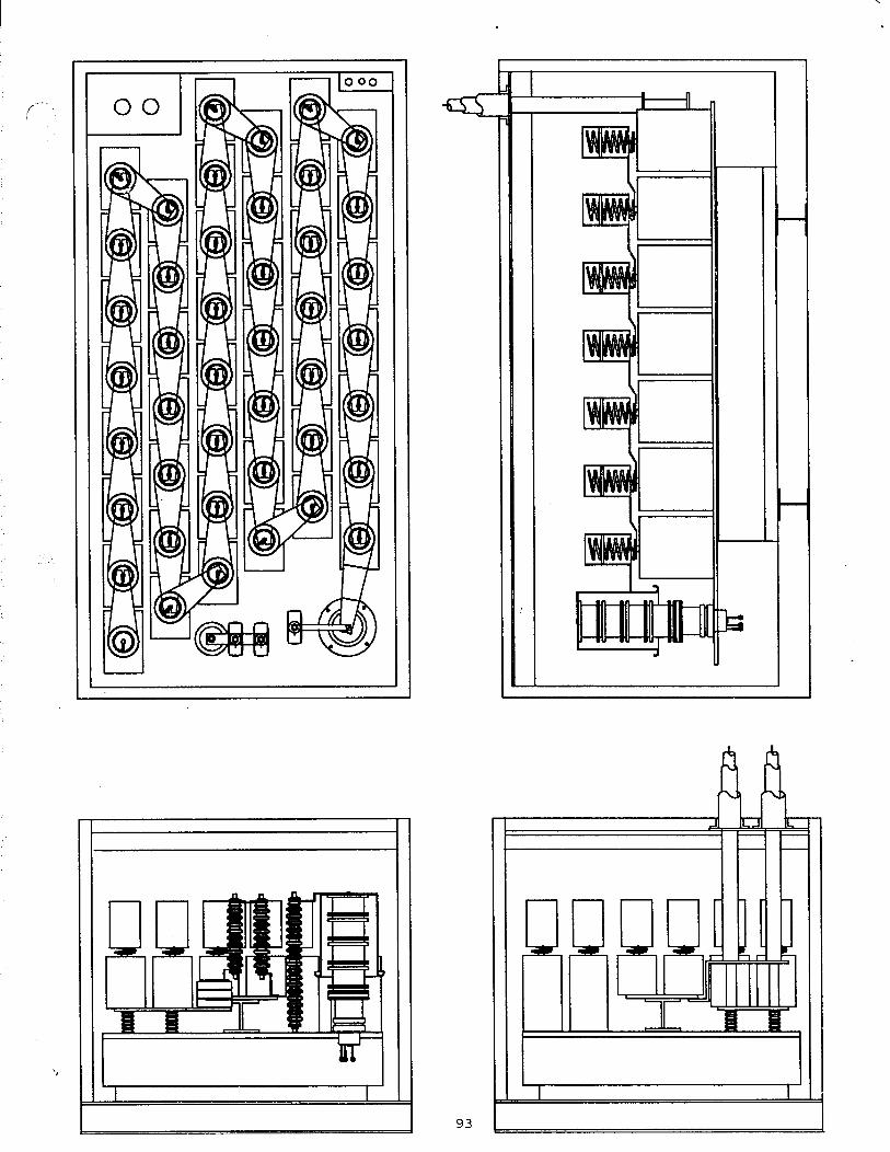
.
.
J00
r 1
I
I I
93
I

,.
>. ,,

.,
..,
., ’-,,’
100
0
–loo
-200
–400
–500
–600
–700
CWL KLYSTRON MODULATOR%0 uhy, 220 ufd 6/1, CABLE—
I I I I I I I I 1 I I I I
o 0.4 0.8 1,2 2 2.4 2.8
(Thoua;~)TIME NSEC
— Sf — S2 — so— KLY VOLTS
●

I I I I I I I I I I -0

L
i
1
-.:-1
i
,,. , I
I
i
I
!
7
i
-
d~~:y~~j-,/-~~ ,
I it: .).’;
‘,
/
/ i
/.O T
I. i !
A ..--—- .-—. -.-... --d—–-—---~—----~—----—~—--—-.------~—--’J— -__...:
:322ns 50ns/di’i ~~8ns. ..... . ... ----. ,. - .-- .-,.. .. ...j ...... ... .._ . ... ...... ........... . .. .. ... . .. .. -.. ....------- -------
; i:sTu58 “!-”~~3~~35’--3cST060060/ 9 ,i~:ST062/9 ~ Page : Rem :, To :Iifm 3
i 2.’4 2GU ~~ou :Oou Single ST06.50.n.s- ;.. 5on.s. - 5.0ns...... ..1 .... 50n.S-. ~ t(a.~tg~.orm. \ .j-..
-?. S:.OJ; ~,’g ‘ier~ical Chant. ‘Jertica: ;
Ilag:Wfm Sel ?0s: }ifnIoou 100 ca~c~i 500
i...,..5Qn9. .. i.... ...-. 1. .. .. . ... .,1 u L..Hf.m_i u I
97

DSA 602 DIGITIZING SIGhiALANALYZERdate: 9-SEP-92 time: 14:50:49
,,-
600V
Ioov/div
! not!trig’d
-400V–356ns 100ns/div 644ns
[~”~ 2: ST042 3: Intg (ST 4:ST033 I Page Rem1 To Wfm 2
L
200V : Ioov 50mU 200V I Single ST042100ns 100ns iOOns 100ns I Waveform
5: ST034 16:Intg (ST 1 Horizontal lPan/ HorizontalMagnify lZoom Pos Gr
Ioov 50mU 2 On 156iOOns 100ns x pts
98
I I 1
‘,

‘,
L
n6u
I
L
m mo0
0
99
.
‘.

I ..i:5.;?
DSA602 DIGITIZING SIGNAL ANALYZER...~.,.
date: i2-AUG-93 time: 10:29:29.~“..
~,~ywti~~6.5x /laKi,- “
L,......~,
‘1’’””~--~——-ii. .,,.
.
:.
I :..,~..-.“.
r.;!:
i
iI
i
I
-....,
i-
~~-~~\,/ i
i!!
-..1.:! –~g~~~ L? qt>,>-- :$4 :.., ~ -,--,.~r,~*’4&t l= ./J: -.
~~ r
-- —.!..
Store Recall I Clear ‘r DeleEe.—
...,.Waveform Waveform ! Waveform Waveform
(.4 i
%} ~~aStore ‘Recall- Delete Main. . Setting Setting Setting Size Zoom Position I.$
i 100n off -210n
L,’.:...,~.,,,,
1 ‘.,’”’sldiv s
:..; <Toll 1 ~L 100., .
:.!

,.
I DSA 602 DIGITIZI!JGSIG}JALA}IALYZER~,Z-..date: 15-SEP-93time: 1~:37:29.,I
2’/
2V/div
L
! not!
trig’d
-18V
1 1 t 1 1 I I I
I 1 I 1 1 I 1 1
-672ns 400ns/div 3. 328us-_._-—-.-—- -----------~’” ‘~~ ‘--”‘--’~---”’H“CSE”’-7 ‘“‘-;y~;”-”–-’\–M=-~su~~: “~s-~atistics ~ ~ern i
I i ments ComP & Def ‘Wf~ !! ~
1-80.0002 ~ 538.0, .~v, . ... ;...–.05.. .-1 Fall i
II~ 330.0 I
IL_.-.s._._--_.– .. .. .... .. --- . .-.
:_i4.7200 ~ ~conkinuous ~ST092._y .1 i----------....... .I .+mO”rizOntal‘?an/ ~tio~~z’;~ta-
i Magnify .Zoom : Pos Gr !i ~ \On~O,..i ._.... ..... .; ~; L- -J pts i
101

.. . .
>
I
i
‘,
.
.
.,
,.
.,
. 102 .
4
..
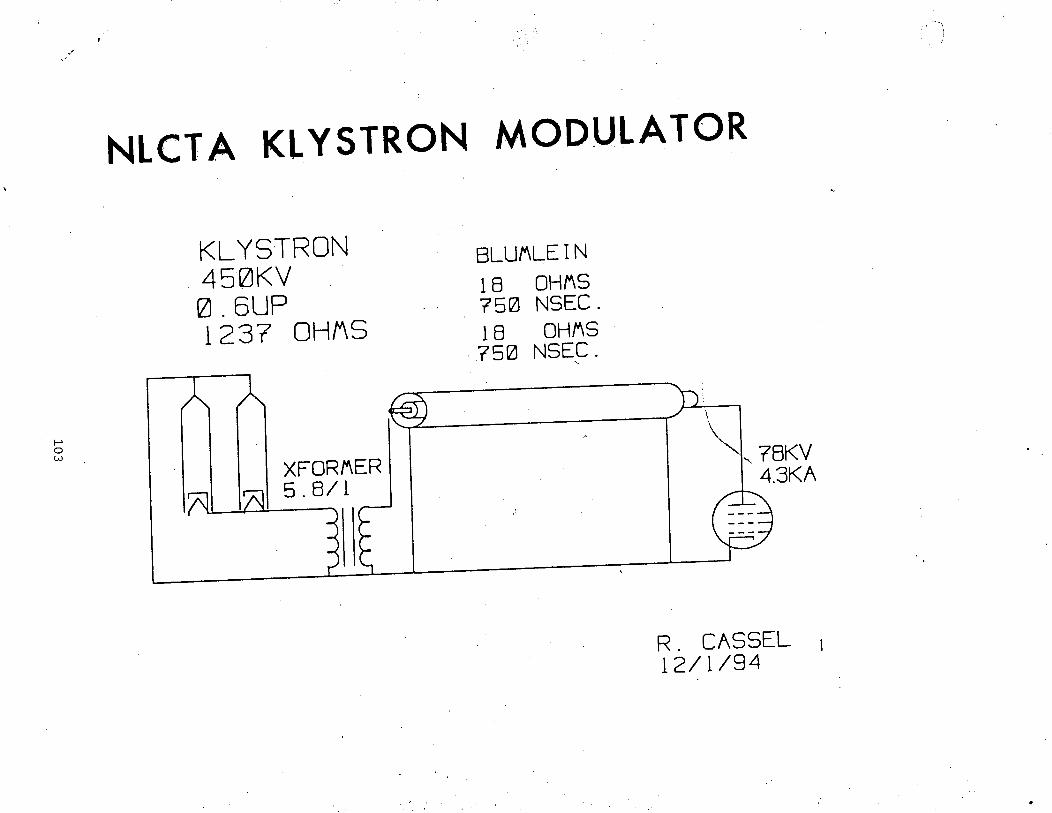
.,.,
I
,. ... ->,
NLCTA KLYSTRON MODULATOR.,
KLYSTRON
450Kv
0. 6UP
123? OHMS
—A-
18 OHMS.! ?50 NSEC .
18 OHMS
?50 NSEC .
P \\,1\
b~?8KV‘ 4.3KA
---------
R . CASSEL ,12/1/94
,,, ..,●

I
,,.,
‘\,
,/
.,
NLCTA KLYSTRON MODULATOR
KLYSTRON600KV
BLUflLEi N 2 LIWS10 OHMS paralleled
1. 2UP 750 NSEC. 6.6 OHMS1076 OHMS 750 NSEC.
$gO Nt::s
R. CASSEL,’
?/5/9 1
...

45000 voltsturns ratiodrive impthy ampsimpedance
Po
stray thym stray ind
70000 voltsturns ratiodrive impthy ampsimpedancestray thystray ind
94000 voltsturns ratiodrive impthy ampsimpedancestray thystray ind
0.75 u-perv 75000 volts60% efficiency turns ratio75 mwrf drive imp
125 mw video thy amps488,359 volts impedance
256 amps stray thy1,908 ohms stray ind
954 ohms 2 each100 nsec76 uhy
1,300
line
22.0 turns1.97 ohms
11,262 amps4.0 ohms
0.400 uhy0.197 uhy
14.0 turns4.87 ohms
7,167 amps9.8 ohms
0.977 uhy0.487 uhy
10.0 turns9.54 ohms
5,119 amps18.4 ohms
1.836 uhy0.954 Uhy
67828 volts7.2 turns
18.40 ohms7,372 amps
18.4 ohms1.840 uhy1.840 uhy
7.5 dielectic50.4 ohms237 feet
blumlein45000 volts
turns ratiodrive impthy ampsimpedancestray thystray ind
70000 voltsturns ratiodrive impthy ampsimpedancestray thystray ind
94000 voltsturns ratiodrive impthy ampsimpedancestray thystray ind
10.9 ‘turns8.10 ohms
11,111 amps4.1 ohms
0.405 uhy0.810 uhy
‘7.0 turns19.60 ohms7,143 amps
9.8 ohms0.980 uhy1.960 uhy
5.0 turns38.16 ohms5,119 amps
18.4 ohms1.836 uhy3.816 uhy
70000 volts 55182 voltsturns ratio 5.9 turnsdrive imp 27.41 ohmsthy amps 9,061 ampsimpedance 18.3 ohmsstray thy 1.218 uhystray ind 2.741 uhy
7.5 dielectic~ 50.0 ohms
548 feet
45000 voltsturns ratiodrive impthy ampsimpedancestray thystray ind
70000 voltsturns ratiodrive impthy ampsimpedancestray thystray ind
94000 voltsturns ratiodrive impthy ampsimpedancestray thystray ind
1.5 mult
7.2 turns18.23 ohms
11,111 amps4.1 ohms
0.405 uhy1.823 uhy
4.7 turns44.10 ohms7,143 amps
9.8 ohms0.980 uhy4,410 uhy
4.0 turns59.62 ohms6,143 amps
15.3 ohms1.530 uhy5.962 uhy > ,,

.-
.
I
----
S=-0
E3
—
00m 0
00y
00y
tI I 1 1 I I 1 1
1
I I
I I
I
I
11[ I
(~I
/
\ I1’
! 1 f
I/ I
I l/l\l
1 I I
II I I ! 1/
/ ! / I 2
I [
tII I I I I I I
I
00N
0 0 0: 0
1y
S11OAO1IY
00y
106
.

\
(
<
Ko
K:..;...;......;.;...;................::
.. ;...;.. .. .
.. ;...;.. .. .
. .. . . ... .
. .;. ..;... .. .i.. .i. .. .. .!. ..!.. I
iii: :.. . . . . .. ... . . ... . . ... . . ... . . ... . . ... . . ... . . ... . . ... . . . . . . . . . . \.. .
. . . . . . . . . . . .. . . . . . . . .:. ... . . ... . . ... . . ... . . ... . . ... . . ... . . ... .. . . . .i...i...i.. .
. . . . . . . . . . . .. . . . . . . . . . .. .. . . ... . . .. . . .:....:..!:.. . .. . . . .. . . . .. . . . {...;...;.. .
:::. . . . . :::: :::: :. .
., ...;: : :
~:
. . . . .. . . . .. . . . .. . . . .. . . . .. . . . . . . . . . . . . . . . . . .. . . . .. . . . .. . . . .. ...{... .:. . . . . . . . . .. . . . . . . . . . . . . . . . .. . . . . . :.. . . . . . . . . . .
. ...!.... . . ..>. ..j . . . . . . . . . . . . . . .: . . .> . . .. . . . .. . . .{....... !. ..:...!...!..
. . . . . . . . . . . . .. . . :. ::. . . :..
. ~...:..:.. .3 . .. . . . .. . . . .. . . . . . . . . . . . . .. . . . .. . . . .. . . . .. . . . .. . . . . . . . .: ...;...:..
. . . . . . . . . . . . .
. . . . . . . . . . . . . ::. .. . .. . . . . . . . . . . . . . . .:. . . <. . . <...<...: . ..!...!...!... . . . . . . . . . . . . . . . . . . .
. . . . . . . . . . . . . .:. . . . . . . . . . . . . . .
. !...!...).. . . . . . . . . . . . . . . . . . . . . . .. . . . .. . . . . . . . . . . . . . . . . . . . !. ..!..
. . . . . . . . . . . . . .:.. . . . . . . . . . . . .
. :...!...:.. . !...>...:.. . . . . . . . . . . . . . . . . . . . . . . . . . . . . . . . . . . . . ..!...!... . . . . . . . .:. . .::: :::. . . . . . . .
. . ...!..... . . . . . . . . . . . . . . . ...+..... .. . . . .. . . . .: . . . . . . . . :...:...: . . . . . .. . . . . .. . . . . . . . . . . . . . . .
. :.. . :.. . . . . . .. . . . . . . . . . . . . . . . . . . . . . . . . . . . . . ...”. . . . . . . . . . . . . . . . . . . . . . . . . . . . . . . . :..
. . . . . . . . .::. :.:. ...
. . . . . . . . .
. . . . . . . . . . . .. . . . .
. . . . . . . . . . . . . . . . . . . . . . . . . . . . . . . . . . . . . . . . . . . . . . . . . . . . . . . . . . . . . . . . . . . . . . .. . . . . . . . . .
:::: ::: :::: :. ::
:.. . :.
. . . . . . . . . . . . . . . . . . . . . . . . . . . . . . . . . . . . . . . . . . . . . . . . . . . . . . . . . . . . . . . . . . . . . :..
,.. . . . . . :::: ::.
. . . . . . . .. . .
. . . . . . . . . . . . -.. . .
. . . . . . . . . . . . . . . . . . . . . . . . . . . . . . . . . . . . . . . . . ...”.. . . . . . . . . . . . . . . . . . . . . . . . . . .. . . . . . . . :::: ::: . . .. . . . . . . . . . .. . . . . . . . . ... ... . . .
. . . . . . . . . . . . . . . . . . . . . . . . . . . . . . . . . . .. ..”...-.. . . . . . . . . . . . . . . . . . . . . . . . . . . . . .. . . . . . . . .::: ::: . . .
. . . . . . . .:.. :.. . :.. . . . .
. . . . . . . . . . . . . . . . . . . . . . . . . . . . . . . . . .“ . ...!..-.. . . . . . . . . . . . . . . . ..
. . . . . .,. . . . . . .
. . . . . :.. . . . . . . .
. . . . . . . . . . .. . . . . . . . . . . . . . . . . . . . . . . . . . . . . . . . . . . . . . . . . . . . . . . . . . . . . . . . . . . . . . .
. . . :;
. . . . . :1. . . . . . . . .. .. . .. . .;...i-..i... :::. . . ii
. .::: :.. . . . . :... . ... . . . . . . . . .. . .. . . t.. . . .. . . .. . .. .{. ..; .$.!...!..
;...,;,~.~..~.. .1
:.. . . . . . .:::.. : . . . . ::. . :...;...: . . .. . . .. . . ... . . ... . . ... . . ... . . ... . . ... . . . . . .
. . . . . . . . . . .. . :. . . . . . .“.!.4.. E..:...!...?.......!...?....... ........;
..;
..i
..j.
. . :::: :::: ““. . . . . . . . . . . . . . . . . . . . . . . .. . . .. . . . .. . . . .. . . . . . ..i . ..{...
. . . . . . . . . . .
. . :.. . . . . . . .. . . . . . . . . . . ., ...>...:.. . . . . . . .. . . . .. . . . .. . . . . . . . i...i...
.. ....3".i...i...;...!...:...:...;...;...;...:...;...!.."l-—
. . .. . . . . . . . . . . . . .. . .. . ... :!..:.. . . . .t
. . :...;...: . .. . .. . .
. . :...:...: . .t
.. i...;...; . .L. .:..
.. i ...;...;. .. . .. . .,..i...i...i.. t
. . .. . . ... . . ... . . ... . . ... . . ... . . ... . . ... . . ... . . ... . . ... . . ... .. . . . . . . . ..::. . . . . . . . . .
..:u.y” .:... j...; . ..j...~ . . .. . ..j . . .. . ..~ . . ... . . :...{.. .
1............:.............>...:...:...:...}................. ............ ........... .....!...:..:. . . } ...}...:. ., >... . . . . ...} . . .. . . . .. . . . . .
. . . . . . . . . .
. . . . . . . . . .
~\ :
::
. . ! ...:...?. . .. ...>..... . .: ...:...} . . . . . . .. . . . :J..i....... .......! ...,
. . . . . . . . . . . . . . :
. . . . . . . . . . . .. . . ~ w:.................................... ................ ....:.. . . . . . . . . . . . ... . . . . . . . . . . .. . . . . . . . . . . . . . . . . ...:...!...:. . . : ...:...:. . . . . . .. . . .. . . .. . . . . . : ...:...!. . . . . . . . . . . . .:. .4.. . . . . . . . . . . . . .. . . . . :.. . . . . . . . .. . . . . .. . . .. . .. . . .. . . .. . . .. . . .. . . .. . . ... . . ... . . . . . . . . . . . . . . :. ...:..
. . . . . . .:: ::. . . :.. . . :6:. ...... .............................................................. ...... . . . . . . . . . .:.. :.. . :. :.. :... . . . . . . . . . . . . . . . E..;..-....................................................................... . . . . . . . ..:: ::::. . . . . . . . . . :L-. . . . . . . . . . . . . . . .: q..:. -... . . .. . . .. . . .. . . .. .. .. . . .. . . .. .. .. . . .....”.. . . . . . . . . . . . . . . . . . . . . . . .
. . . . . . . . ..:: ::::
. . . . . . . . .
:.. . . . . . . . . . . . . . .
‘,
107

1.
,7“
,., —
NLCTA ~YSTRONMODULATOR
R. CASSEL
12/14/92
WATER DIELECTRIC LINEANDREW CABLE.
W AND 5 HELl~” AIR-DIELECTRICCABLE
‘,
108

..
ANDREWS CABLEklystron line calculations
:Iystron490.0 kV954.0 ohms513.6 amos251.7 Mw
ransformer7.1 ratio
blumlein—.69.5 kV
3,621.1 amps19.2 ohms
hyratron“ 69.5 kV
7,242.1 amps- 9.6 ohms2 parallel 18
<Iystron490.0 kv954.0 ohms513.6 amps251.7 Mw
transformer6.7 ratio
blumlein73.1 kV
3,441.3 amps21.3 ohms
thyratron73.1 kV
6,882.6 amps10.6 ohms
,.,
,.,,
BLU~E~
1.2 usecoil oilblumlein blumlein
INSIDE OUTSIDE INSIDE OUTSIDE
voltage 70000 70000 volts 73000 73000 volts
LENGTH 226 226 feet 226 226 feet
HJ450 I HJ9-50 I HJ5-50 o HJ8-50 O
IN INSIDE 0.603 1.316 inch 1.570 2.500 inch
IN OUTSIDE 0.713 1.550 inch 1.830 2.850 inch
INNER 0.658 1.433 inch 1.700 2.675 inch
HJ450 o HJ9-50 O HJ8-50 O HJII-500
OUT INSIDE 1.316 3.365 inch 2.500 4.440 inch
OUT OUTSIDE 1.550 3.840 inch 2.850 5.000 inch
OUTER 1.433 3.603 inch 2.675 4.720 inch
insulation 0.603 1.08475 inch 0.4875 1.0225 inch
volts/roil 116 65 vlmil 150 71 vlmil
LOG 0.83 0.83 0.45 0.47
1 1 1
INDUCTANCE 0.05 0.05 UHY/FT 0.0: 0.03 UHY/FT
TOTAL L 11.44 11.50 UHY 6.27 6.46 UHY
6.80 6.80 6 on
138.ZO PF/FT 253.52 245t
‘--- - ‘FD 57.38 5a
IDIELECTRIC 6.80 ).OU
CAPACITANCE 138.96
J
;.86 PFIFT ‘
TOTAL C 31.45 31.28 Ml .5.64 MFD
IMPEDANCE 19.1 19.2 OHMS 10.4 10.8OHMS
SQRT(L/C) 19.07 19.18 10.45 10.78A-I-,, 9 CGI 7651 nsGrJfi 2.651 2.651 nsedftuclay I &.wu . I ---- -
11-7------
I I
.’-\

,
.
z
/“/
—
‘,,
110

I
.’
o
\ I
-.
‘,
I oz
vz
L- —
r——–
I I

/..1
,..
I
—
..-
I
0
spuesnoql
VW/ S11OA
112
0
o
‘\\--
c,

1 I I I i I 1 I I I
No0
0
●
‘,
113
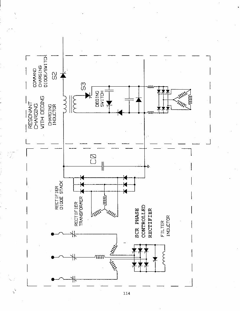
.
—— —_ __ __1
I
I
I
I
I
J
L
—— —L —— —
r—— —— —
- +
‘1
I
I
I m
I
I
I
I
I
I
I
I
A7
— .11 P- I
I
_A
I....,
L —— —— —— __ _‘,‘> 114

,
.m
>%Y<
. m
4
t–l+
c
m●
>1<
.115

.:..:
::
(
‘,
NLC MODULATORCABLE BLUMLEINoILE=7.5n.5 MS
RESERVOR
‘HY HEATER
(LY HEATER
C~TROLS
1 1 I I 1. I
—1
R CASSEL1VW94
116

I
.
‘,‘;
ma
a a am
c
117
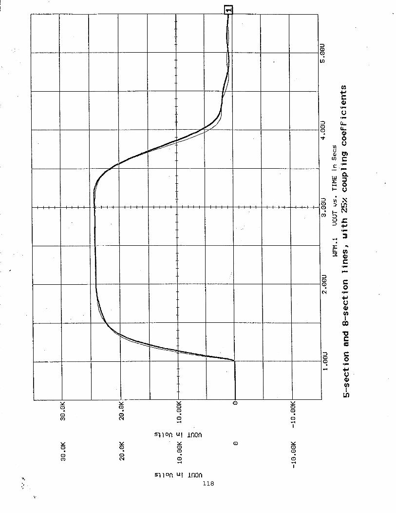
{ F t +
a
Lnon118
+

i
4
i
119
+ t

NLCTA =YSTRONMODULATOR
R. CASSEL7/12/94
MANAGEMENT DECISION
● BU~D CON~NTIONAL TYPEMODULATORFORNLCTA
c ACCEPT SLOW mSE TIME MODULATOR
● ACCEPT ~SULT~G LOW EFFIC~NCY
● USE AS MUCH AS POSSIBLE STANDARD SLAC DESIGN ANDPRO~N COMPONENTS
● TWO KLYSTRONS PER MODULATOR 200 MW 1.5 pSEC (RF PULSE)1000 JOULES ~ PFN (i.e. efficiency <60V0 )
● 4 MODULATOR WITH TWO POWER SUPPLmS FOR 180 PPSOPERATION, OR 360KW PER POWER SUPPLY
‘,.;
120

KLYSTRONHOOULATORPULSE FORMING NETUORK
E= 1000 JOULES, T=2 .4 USEC
1(U2)lmI
28
El.M
2
Q5
.Em:‘L
m K=L1lS L116
L1lS L116 L117 II L118 II L11O.W.o.w.o.m .O.m.o .Om
84 es 86 87 ee
-—
m K36 K35 KWL1~ L126 Ll= L1~
Ll= . ~ L126 L127 L136 Ll=.- .M.o.m.o .W”o.m
96 9? 08 00 100
—K1 w I
K3 K4L2 L7 LS LO
L2 L7 L8 LO L1O.m.o.-.m.m .o.~.o.m
—
..
121.

..
>..,
CHARGINO~~~P~~RLINE
SV I TCH 1,4 OHMS ‘—— — — ‘— — —— 4SAFETY
DISCONNECT ~- CHARGI~INDUCTOR
Iu
I
II
IRECTIFIERDIOOE STACK
4 ‘each
5.6QPFN5 SECTION—..__.--
1
;t
DEQU I NGENERGYRECOVERYM
I
I
~ FILTER
T
CAPACITOR
I
RECTIFIER
TRANSFORMER w
I L I r L- 1 1I 1 [ I
, 4 I
II Is I 1.4B0V OPEN VYE
1=r + ~1 I I 1 I
2 eoch
ml
>i------THYRATRON50 KV
. 8400 AMPS ,,,,,,L
FILTER
480 V 3PH I NOUCTOR
I
I
I
4 t
1 . P~SE TRANSFORMER24 KV TO 500 KV21/1 2.5 uSEC.
[’iT
J
KLYSTRON MODULATnn
..— ————9/05/94 I ~IR~~
.

I
n
III(Y
PULSE TRANSFORMER21/1 TURNS RATIO500 KV/ 24 KV
800 A / 16.8KA 2.5USEC
85 A RMS/ 415 A RMS t
I
,
—
—
i-
KLYSTRON500 KV
A
#[ #2
A
400 AMP1. 5uSEC
-——
%. w———_—————— —10 &o Ih
Mm
Ill u I Ill um Pkb b
11 - - ,, m - - ,, — , ,1 - - ,,9 - . ,, —,, 14 ‘1
I
1 1 I , , , , ,i I I I I I I I I I 1
( tA L L
— I , , - m ,, - ,, — , ,, - . , ,,— ,,
*I #2/ ‘‘--‘~tiTT
—
-Gme ‘ ‘-FIGURE 2
123
1 I
30 AMPSKLYSTR~
H~TER40v/4M

.
I
\
/
L/\
\
PULSE TRANSFORMER
R mmrmYm
w~A
END VIEW/
{ SECONOARYCORONARM
f
.
—
r1 r , f ?
\PMY WNINGSC~N WRESr RE~N CO~N \
- MTER- MTER
L 1
SIDE VIEW
m...........Q. . . . . . . . . . . .
- TRGGER
- SENSEW- W ALNE
‘“ ~::H- RESERVOR.........................- R~RN SH~ /
+2rw+
/
TOP VIEW
// FIGURE 3
‘,,;
124

,,
.
w mm
NLCTA MODULATOR
E‘,.
125

I . ,..

Specifications
Outputpu~ voltage 600 kVOutputpulsecurrent 1200 AOutputimpedance 500Q c>2M#mw)
Pulse rise time 150 ns
Pulse length(flat-top) 400 ns
Pulse amplitude drift < 1.0 %
hlse repetition rate 50 pps
127

.
a
‘\ \
m Hill
aoL
—
128

‘\/
.
KLYSTRONLOAD500 n
DISCHARGE UNIT ~

HIGH-VOLTAGEELECTRODE
GRWND ~ELE~RODE
d dQ .6.12
zm
‘2~-
&-tT
w
* 1
“I* 8n
130

760e >
I
.
..
..
.I
I
!
131
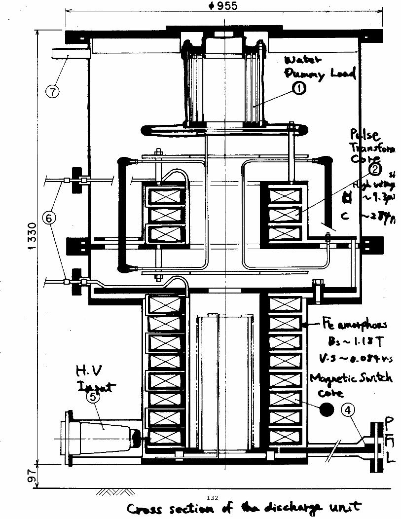
I +955
II
TI
I

D;%*r -----------
“MAGNETICSWITCHP
I PULSEt
ITRANSFORMER
I 1:15
1
DUWYLOAD
1
.——- —--- -- .0 --00-0 0 ------- J
I
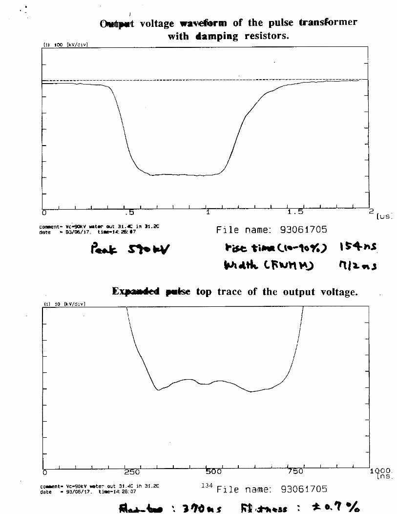
b4
m~ voltage wav~m of the pulse tiaastirmerwith damping resistors.
-------------------------------------------------- ------------- ------------ ———------ ——----—-———
I I 1 1 I 1 I 1 I I1 I 1 I I I 1
II 1
. 5 1 1.5 2[us:
E~ ~k top trace of the output voltage. .
1) 10 [k V/d Iv]
I I f I I) 250 0
~?1 00.
ns.
Co-nt= Vc=90kV -ter out 31 .4C in 31 .2Cdate = 93/06/i7. t iw-i4: 2607 134 File name: 93061705

New loss-h de-Qina vstem
Power loss of deQing system(pdeo)
(bo.5)
k=l– V- (mgulatd)VPm(umegdatd)
Ct : Totil PFNVPFN : PFN ~v::fF)
f~‘w-)k:
Power loss for full-se ~ ~qC.UNGeV)
Total power loss=4.lkw x 1~.UW(H ~er)
1. ~ k a ~ cimh with low-voltage
comFm2. It is igh energy remvery ~ d Rs
rassive circuit.
3. tk~bletom~~~~ power.
JLC-ATF ~135

I
AC UNE
T
PFN
rlPFN
MAINDC
F
JU-ATF136

I
Loss-free de-Qingwaveforms
JLC-AW ~ -137

KLYSTRON
H. MATSUMOTO, H. BABA and T. SHINTAKE
KEK
K. WATANABE
TOHOKU UNIVERSITY
P. PEARCE
CERN
M. H. CHO, J. S. OH and W. NAMKUNG
PAL
) LINE~ COLLIDE=
138

LC
LINEAR COLLIDER PROJECT......................................................................................................................................................................................——..——-,..,.,—.....-—...-.—..-—---.—,.—.--.-....—.—2 GeV
POSITRON1.1-1.5 x Id”
PRE-DAMPING RING / ELECTRON
/
POSITRONJlllll:\lll@ “b 2 GeV
2 GeVDAMPING RING TARGET 72 bunches x 50-150 Hz T 1 72 bunches x 50-150 Hz DAMPING RING
I2.8 ns 2 GeV
~ e-DETECTOR 02=5 mm
MAINLINAC FF FF MAIN LINAC “’=80 ‘lm t
I ~Wy = 310.03 x 10⁻⁶ rad~m &WY= 310.03x 10⁻⁶ rad=m ~BUNCH BUNCH
COMPRESSOR2 km
COMPRESSORPw 1 n 1 -Q
4
25 km
BEAM ENERGY (C. M.)LUMINOSITYTOTAL LENGHTNOMINAL ACC. GRAD.NET ACC. GRAD.TOTAL WALL PLUG POWERRMS BEAM SIZE AT IP (fly)CROSSING ANGLEDISRUPTION PARAMETERNUMBER OF BEAMSTRAHLUNG PHOTONSENERGY LOSS BY BEAMSTRAHLUNGPINCH ENHANCEMENT FACTOR
LC1 LC2500 1000 GeV9.1 6.3 10A33/~mA~~
25 25 Km41 58 MVlm30 43 MVlm220 220 MW260/3.0 3722.2 nm6.0 6.0 mrad0.20/17.5 0.067/11.3 DtiDy1.5 1.45.3 8.0 0/0
1.6 1.5
FINAL FOCUS~ FFTB AT SLAC
MULTI BUNCH DAMPING RING
~ ATF AT KEK

d
WILC
<:c”Li:;~Q,w= 500GEV MAIN LINAC IN C-BAND CASEG* &9,~s~*, __LC .................................................................................................. ..........................................................................................................................................................................................................................................................................................—.—— —.-, —,-—---. -.--—, ---,,.,,...... .. . .... --- . . ..... ..- . ... . . . . ..-...-.
AC POWER LINE
1 150
POWER SUPPLY
50 KVAI
(SLEBII OR SLE~l & PHASE RAMP)
TEo.,.~, 2a=20cm, L=4m, 8 CELLS
MODULATOR ISWITCHING
POWER SUPPLY
~ 175 Mw 350 KV,317A, 150PPS 175 MW
0.48@ ~ = 45~0, pp = i. 53 0.48 @
MODULATORS 4,356
KLYSTRONS 4,356
STRUCTURES 8,712
ACTIVE LENGTH 15.6
WALL-PLUG POWER 220
/
=
y Ea=30 (41) MVIM
3z14, alk=O.13-0.1 7, vg=O.012-O.035c, r=55 M~m, Tf=280 ns,r= 0.53
ALIGNMENT TORELANCE: 35 ~lm I STRUCTURE
UNITS 12LINACS
TUBES 12LINACS
UNITS 12LINACS
KM 12LINACS
MW 12LINACS
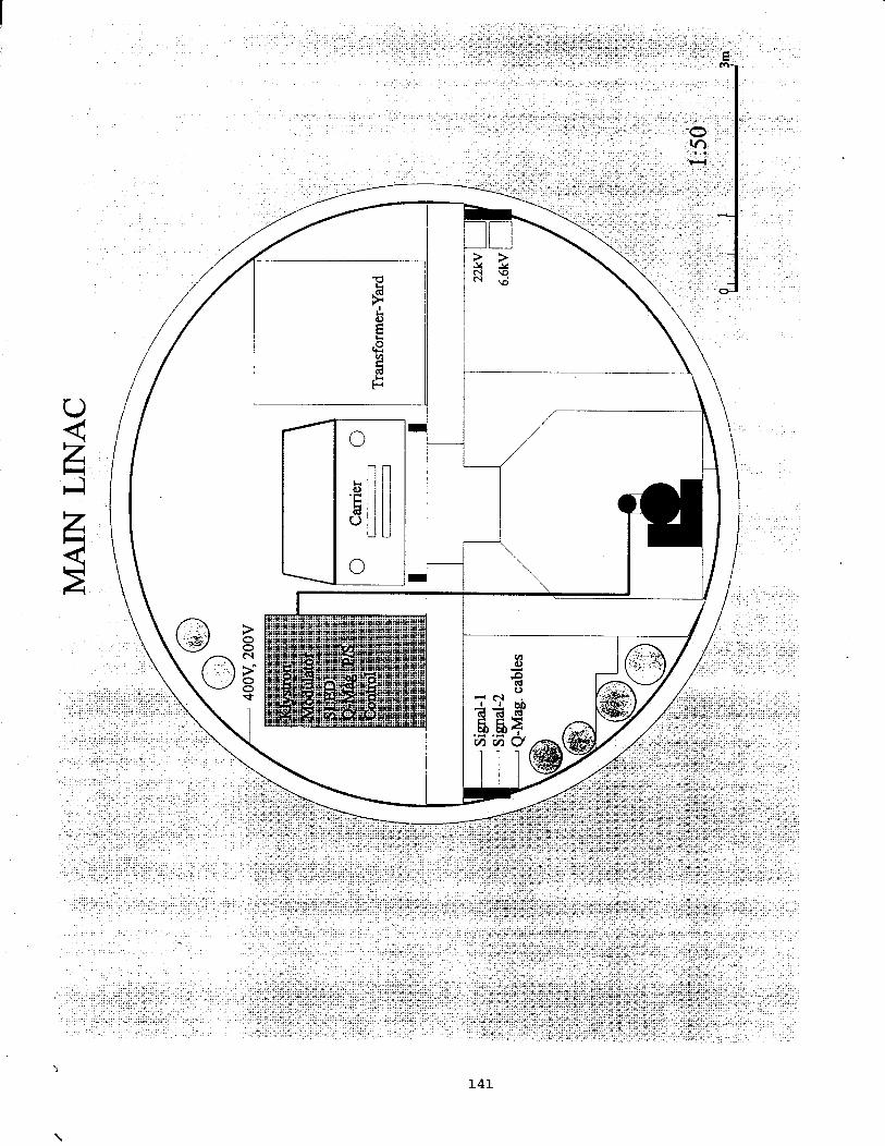
L’ ‘“
~: :... J)o-
.8Eu11 ....0
+ \\<,:,.: ,..,..::..
\

VERY IMPORTANT DESIGN CONSIDERATION IS
IMPROVING THE OVERALL SYSTEM SUCH AS
● RELIABILITY
c AVAILABILITY
● MAINTAINABILITY
BECAUSE, LINEAR COLLIDER SHOULD BE
USE MORE THAN THE 4000 KLYSTRON
MODULATORS AND TUBES
‘,
\
) LINE~ COLLIDE=
mBEwlw5
142

J
zLC
‘“’’%oo’ CIRCUIT OF THE C-BAND KLYSTRON MODULATOR%’+:L&?,~
AC
FILTER DE-SPIKING PFN :16CHOKE CIRCUIT I
CELL X 2 ( PARALLEL)33 nF, 496 nH
152 kJ/s at 150 pps
DC HV SWITCHINGPOWER SUPPLY
POWER LINE
—
TAIL
SURGE DESPIKER
+
THYRATRON — :
1:16
1 LINE~ COLLIDER~199WWTOBEWM

,,
‘\ !
ICAPACITOR CHARGING POWER SUPPLIES
20
SPECIFICATIONS
MODEL I 203 I 303
Output Voltages/Current
o-1 kvo-2 kvo-4 kvO-5 kV
0-10 kV0-20 kV0-30 kV0-40 kv0-50 kv
50 A
25 A
13 A
10 A
5A
2.5 A
1.7 A
1.3 A
1.0 A
Charge Rate
average
I
20 kJlspeak 25 kJls
Input POW(
340-460Vor432-528V50-60 Hz,3 phase
Polarity
50 A max
40 A max
Positive or negative
Voltage Regulationt 0.5?0 to 200Hz
Efficiency
75 A
38 A19 A15 A
7.5 A
3.8 A
2.5 A
1.9 A
1.5 A
kJ/s to 30 kJ/s
30 kJls37.5 kJls
N.A.
60A max
Inrush CurrentLimited to below fullpower current
ProtectionShort circuit, arc, over-temp, over-voltage, accessinterlocks, highly buf-fered 1/0. Protected fromexcess voltage reversal.
CoolingWater, 35°C max at >2.0gallons per minute.
Temperature RangeOperating: 10°C to 50‘C(Lower temperatures onspecial request)Storage: –55°c to 700c
Size19 in. Standard rack
mount17 in. (430mm) Wide
12.25 in (7U) High22 in. (560mm) Deep5 in. for cables.Other package configura-tions avaflable on request.
Weight185 lbs.
POWER REGUUTION
Usable output power vs.output voltage setting
$ I% /
7
5
2
u
Fullscale outputvoltage _
For a given capacitor andrep. rate, these modelsprovide constant outputpower over the top 25R ofthe output voltage range.Below that it providesconstant current.
ALE’s unique control cir-cuit maintains the cons-tant output current in-dependent of he voltage.
For High Voltage Capacitor Charging SuppliesFrom 500 J/s To 30 kJ/s
Advancedhigh voltage current sources spec~lcdy designed to charge capacitors in discharge driven apphcations.
MODEL CHARGE RATE MODEL CHARGE RATE
500 500 jls 402 4000 Jls102 1000 Jis 802 8000 Jls152 1500 Jls
ALSO AVAILABLE
YAGDRIVE SUPPLIESCW Arc Lamp Supplies
4kW to 8kW
co~Ballastless COZ Supplies
250W to 1000W
144 03-100-008


.
4
‘LC
e
~L@fc&
~L@’ G+op C-BAND 5U MW KLYSTRON MODULATOR~d~ LC
INTER LOCK—
RF CONTROL
FOCUSING MAGNETPOWER SUPPLY
THYRATRON CONTROL
DC HV SWITCHPOWER SUPPL
~–.–.....*... .. .........
CABINET SIZE:2m(H)x lm(W)xl.5 m(D)
PFN :16 CELL-PARALLEL,33 nF, 498 nH
THYRATRON :43 kV X 5072 A
2.lm
:,
—*-
HEAT EXCHANGER 350 kV, 317 A, 150 PPS
COOLING FAN ~ =45Y0, pP=l .53
— — LINEM COLL~ER ~
1WWmTOEEW@

.,
LINAC PA>
PLS 200MW MODULATOR UPGRADE SYSTEM
I I
PFNSECTION
LAYOUT
!
LC Resonant Charging
HV DC Power Supply
PFN Capacitor
PFN
\ /HV DC POWER SUPPLY
SECTION
Command Charging
Inverter Power Supply
High Energy PFN Capacitor

MODULATORS AND SWITCHED MODE POWER SUPPLIESG. BEES
“;?-s--r-
c
A

. .
,-
—
.,
i...
149.

1
. I——
..
150
,,..
,. -

ELECTRONICMEASUREMENTS,INC.
HV CAPACITOR CHARGING SUPPLIES
SERIES 402 ● O-1kV to O-50kV 4,000 J/s; 6,000 Watts Constant VoltageSERIES 802 ● O-1kV to O-50kV 8,000 J/s; 10,000 Watts Constant VoltageProducing voltage ranges between O-1 kV to 0-50 kV, these supplies produce ~ Jls (42) and 8000 Jls (802) average chargingrates for direct capacitor charging of both repetitionrate and high energy, single shot epphcations. They will dso reliabw drive con-stant Voltage Loads such as Magnetrons, Ms and Electron Beam Sources.
All units incorporate IGBT inverter technology for trouble-free operation with protection against arcs, shofi and open circuitconditions.
● Fully adjustable output voltage ● Simple parallel operation for upgradeable increased power
● Worldwide input vohagedfrequencies ● Positive and Negative polarity
● LocaUremote control as standard ● Repetition rates to 1 kHz and more
● Compties with UL, CSA, VDE safety requirements ● Tight regulation
SERIES 203 ● O-1kV to O-50kV 20,000 J/s; 30,000 Watts Constant VoltageSERIES 303 c O-1kV to O-50kV 30,000 J/s; 50,000 Watts Constant Voltage
FEATURES:
● Only an incredible 12X” in 19“ rack height
c Modular internal construction
● Full protection against open circuit, short circuit, Arc
* Remote andor local control as standard
● High efficiency
● Parallel operation for increased power
o ● High Voltage Engineers please note
@~ In many applications the 203/303 Series can+%
be used to generate 50W average DC power!Contact our technical department for detaila.
405 ESSEX HOAD, NEPTUNE, NJ 07753 ● PHONE: 908-922-9300 FAX: 908-922-9334
15103-1WO1O REV

\
CAPACITOR CHARGINGPRODUCTDESCRIPTIONThis series of high voltageswitching power supplies isdesigned to quickly chargecapacitors and pulse forming net-works. Advanced semiconductortechnology, combined with highquality construction, yields ex-ceptionally small and reliablepower supplies. With many stan-dard features and options, thisseries is useful in a wide varietyof OEM and laboratory applica-tions. Designed for continuoususe in severe electrical en-vironments, these air cooledpower supplies provide anaverage charging rate of 4.o to8.0 kJlsec over nine outputvoltage ranges from lkV to 50kV,positive or negative polarity.Output control and statusmonitoring are easily accom-plished with the standard remoteinterface or the optional frontpanel controls.
OUTPUTVOLTAGES
lkV to 50kV in the followingranges: 1,2,4,5,10,20,30,40,50
Charge Rates U/s)Model Avg. Pe&
402 4000 5000802 8000 9000
1/2 CV2Peak charge rate = ~
c
Average charge rate = 1/2 CV2
‘P
APPLICATIONSLaboratory Unit
402L and 802L have full frontpanel instrumentation forlaboratory or prototype use. In-cludes voltage adjust, digitalvoltage and current meters,quick reference voltage and cur-rent bar graphs, high voltageON/OFF, power switch, view-setswitch which allows previewingof output voltage setting, statusindicators.
402L CONFIGURATION19“
—-.●
✌✎✎✍✎✎
I,,,
802L CONFIGURATION,9,,
I
OPTIONALCONFIGURATIONS
Remote Control Only
For use as a stand-alone or inpardel with laboratory units forincreased power. Has powerswitch and status indicators.
OEM Blank Front Panel
Remote operation only. Used inlow cost high volume applica-tions. User supplies all controls.
Consultfacto~ for modificationstothe standard configurations orcustom requirements.
HIGH VOLTAGEPOWER SUPPLIES4 to 8 kJ/s
MODELS 402802
■ 5000 TO 9000 J/S PEAKCHARGE RATE
■ COMPACT LIGHTWEIGHTDESIGN
CONSTANT CHARGERATES INDEPENDENT OFLINE VOLTAGE
FULLY ADJUSTABLEOUTPUT VOLTAGE
WORLDWIDE INPUTVOLTAGES
MEETS UL, CSA, VDESAFETY STANDARDS
EXTREMELY LOW STOREDENERGY
PROTECTED AGAINSTOPEN CIRCUIT, SHORTCIRCUIT, ARC, OVER-TEMP, OVER-VOLTAGE
SIMPLE PARALLELOPERATION FORINCREASED POWER
405 ESSEX ROAD, NEPTUNE, NJ 07753 ● PHONE: 908-922-9300 FAX: 908-922-9334
152

!
‘,
CAPACITOR CHARGING POWERSUPPLIES4 kJ/s to 8 kJ/s -
POWERREGUUTION
SPECIFICATIONS
IMODEL 402 802
Output Voltages/Current
o-1kvo-2 kv
o-4 kv
o-5 kv
o-1okv0-20 kv0-30 kv0-40 kv0-50 kv
10.0 A
5.0 A
2.5 A2.0 A1.0 A500 mA333 mA250 mA200 mA
18.0 A
9.0 A
4.5 A
3.6 A
1.8 A
900 mA
600 mA
450 mA
360 mA
Charge Rate
average 4.0 kJls 8.0 kJlspeak . 5.0 kJls 9.0 kJls
Input Power
180-264V 20 A max 40 A max
or
340-460V 15 A max 25 A max
50-60 Hz,
3 phase
Size
19 in. rackmount by 7 in. (4U) high 8.75 in. (5U) high17 in. deep
Weight ]40 lbs., 18 kg 185 lbs., 40 kg
Polarity
Positive or negative
Regulation~ 1.0% to lkHz standard
Efficiency
85% minimum at full load
Power Factor
85% minimum with 180-264 VAC line
Cooling
Forced air, – 20 “C to 40 ‘C inlet temp, 10%to 90% R.H. non-condensing
OptionsFront panel controls, rack
mount slides, AC contac-tor (OEM ONLY). Water
to air external heatexchanger
Inrush CurrentLimited to below fullpower current
ProtectionOpen circuit, short circuit,arc, over-temp, over-voltage, access interlocks,highly buffered 1/0
Usable output power vs.output voltage setting
7Y% I m“.
Full scale output vo!toge J
Variation of charge wave-
,,fime
ALE’s unique control cir-
cuit maintains the con-
stant output current in-
For a given capacitor and
rep. rate these modelsprovide constant output
power over the top 25% of
the output voltage range.Below that it provides
constant current.dependent of line voltage
For High Voltage CapacitorCharging From
500 J/s TO 30 kJ/s
mMODELS MODELS
500 FOR 500 J/s 203 FOR 20 kJ/s
102 1000 J/s 303 30 kJ/s
152 1500 J/s
153

MODULATOR EFFICIENCY, RINGING, PF~s VS PFN’s
T. BUWES
154
t 4

-l—
, .,
,.
\\
\

I
.
156

——
*
157

-...
,,
>..
158

I ‘--— —.— ——__
COMPACT AND EFFICIENTMOD~ATOR DESIGN
Basically, If you wantcffici,ency, your system must be compact. Exctis volumeequates to leakage reactance insome form or other. The B Iumlein approach certainly is no[ the best approach from anefficiency standpoint as Burkes pointed out. I suggest that you build the modulator usinga vuiation on the approach used in the Damping Nng kicker. See figure 1.
~d . R.-.?T .. —l. nen< —
*iiF”“--’”‘--’If you use a 14/1 pulse transformer, the PFL can k opera[ed at 75kV wi[h a
6~ impedance, If ~he PFL was made in the form of a stripline with slabs of stron(iurn‘932) as the dielec(ric, i[s length would be about 40 feet. To operate at 75kVtitanate(=, –-
the dielectric thickness wouid have to be no less than 1.j” thick on each side and would
r~uire several intermediate grading electrodes to maintain a uniform field across tie
dielectric, particularity at the edges. The width of the center conductor would be a~~ut 3“
for a 6~ PFL. The PFL could be made tunable over a limited range by using movablesides to adjust the inductance of the line. The whole works could be externally clamped tomake good contact with the dielectric and filled with SF6 or a Iiquid dielectric A flexibleboot along the sides would contain this dielectric. The end-uf-Iine clipper could bedistributed in[o this structure by connecting diode wafers and resistors in between thegra shown in figure 2.
Grd. - rc>,”j-e=
Gd
El 2CTWJ ej
CiamyJ~.TJ~ur& 2 ~ti$.C~i.~
cll;pc-
Finally, to prolong thyralron lifetime, a saturable reactor can be made to helpin two ways. Firs[, it can be dejigned to limit thyratron current during turn-on to [hereactor magnetizing current. Following the pulse, it will again limit any reverse curren[
due [o mis-match. This will eliminate the need for the reverse diode on the anode. Tomake [his reactor function properly, it is reset by lhe Pm charging current (chmgingsupply connected to the thyratron anode). The Pm discharge current resets the reactor inthe opposite direction so that i[ can block reverse currents and the cycIe repeats.
159John Dinkel/FermilabOctober 16, 1995

SUMMARY OF MODULATOR EFFICENCY SESSIONG. Leyh
R. Cassel discussed the performance, cost, and efficiency requirements forthe Next Linear Collider (NLC), and identified causes of inefficiency and expensein the existing SLAC modulator. Transparencies of conceptual designs for theNLC Modulator and simulated waveforms were presented.
Cassel stated that the performance specs of the existing SLAC modulator(efficiency < 50Y., cost > 250k$) will not be sufficient to meet the construction andoperating budgets of the NLC, and suggested a design goal of 80% overallmodulator efficiency, a rise time of e 200 ns, and a per modulator cost of < 180k$.
The objectives for the NLCTA Modulator were presented as follows:Klystron Test Modulator - 600kV, 560A, 1.2pSecNLC Test Accelerator (NLCTA) Modulator - 480kV, 400A, 1.5LSecUpgrade to 600kV, 560A, 1.5pSecDevelopment Modulator for future Linear Collider
Q: Regarding using Andrews cable as oil-filled Blumlein. Will there be a potentialproblem with surface breakdown between the plastic supports and the oil?A: LLNL has successfully used this type of cable as a water-filled Blumlein, but at alower voltage.Q: Why don’t you use water (higher dielectric constant) rather than oil?A: The dielectric constant and strength of water varies significantly withtemperature, and with the purity of the water. Also, pulse charging would berequired with a water Blumlein scheme.Q: Can magnetic shaping be used to improve the rise time?A: Yes, but a non-trivial amount of energy would be reflected by the pulse shapingcircuit in the process. How would you recover that reflected energy?Q: Can the 100pF of ‘stray’ capacitance on the klystron cathode be incorporatedinto a lumped transmission line in order to reduce its effect on overall efficiency?A: Much ~ffort has gone into minimizing this stray capacitance, but the close -cathode to anode spacing plus the proximity of irregular objects (such as ionpumps) place limits on how much the cathode capacitance can be reduced. Ofgreater importance is the cathode voltage, since the stored ener~ on the cathodestructure is l/2CV2.
George Bees introduced EMI’s product line of switched-mode capacitorcharging power supplies, and presented transparencies outlining the pros andcons of various modulator topologies, with and without switched-mode powersupplies (SMPS).
160

The 3 topologies discussed were:A. The SLAC-type modulator (60Hz PS followed by a resonant charger)B. An SMPS capacitor charger followed by a resonant chargerC. An SMPS capacitor charger which charges the PFN capacitors directlyTopologies B and C were compared first, followed by a comparison of A
and C. The claimed advantages of each topology are as follows:
B. -
c.—
A. -
c. -
More efficientSMPS costs about 0.4 to 0.5 $/W (Compare to scheme Cat 0.8 to 1.0 $/W)
No large capacitor across PS to dumpPS latch-up avoidedLower pulse transformer ratio may be possible
Second Com~arison
Well understood, reliability data available
Modular, N+l architectureNo De-Q’ing circuitry requiredActive power factor correction available (>0.95)~erent current limiting, low stored energyAvailable ‘off-the-shelf
Q: Has anyone ever used SMPS capacitor chargers in the direct charging scheme,
in a real modulator?
A: Yes, John Kinross-Wright at LANL uses 5 of the model 303 cap chargers in
parallel, in a modulator operating at 10Hz.
Fred Nylander talked about matching the pulse transformer to the PFN,and pointed out that if the impedance of the pulse transformer is set to 0.6 timesthe characteristic impedance of the PFN, then the overshoot on the output will beindependent of the load impedance.
Magne Stangenes suggested a pulse transformer design using core bias inorder to reduce the leakage inductance enough to meet this criteria.
161

I
ROW TAELEDISaSSION OFMOD~A~R-KLYS~ON P~~RS
Responses compild by G. tiyh .
TOPIC 1:Tony Donaldson asks the assembly, “So, will it be possible to build a machine with 2000modulators, and ~ Mystrons?”Harish Anamkath, Titan Beta - Expresses his position that reliability is more important thanefficiency.Chris Pappas, Brookhaven - Yes, if enough dollars are avadable. Energy recovery horn themodulator will probably be necessary.Dick Cassel, SLAC - Higher modtiator efficiencies can be obtaind, for more money.Greg Loew, SLAC - The design tradeoffs that must be made will depend upon the country inwhich the Linear Colfider is buflt, and the resources which wi~ be available at the proposalsite.Chris Waters, Pearson - The pulse transformer losses can be made quite low, if enoughresearch do~ars are avadable. Present desi~ns are almost o~timum.Jud Hammon, Physics International - Usin~ a Bludein at higher voltages will produce abetter rise time. Jud descri~ a modulator system that is in use, which operates at 500kV,150 to ~ Joules/pulse, 100 pulsedsec, and has rise times of 150 to 500 ns.Hugh Menown, EEV - Higher voltage thyratrons wfil allow faster rise times, and greaterefficiency.Ron Sheldrake, EEV - Use a 500 kV thyratron and eliminate the pulse transformer.Torn Burkes, Pulse Power - A Blutiein is not a good choice for an energy efficient machine,since the switch current is much higher than the load current. Higher voltages on tiethyratron would be better. Tom states that he has had good experience with switched-modecapacitor chargers, and that they offer better diagnostics and adjustability than conventionalsupplies.David Turnquist, Litton - Agrees with Burkes. Double the switch voltage rather than use aBludein.Mitsuo Akemoto, KEK - Showd transparencies outiining a scheme for recovering the De-Qing energy back into a ‘Sub PS’, which bootstraps the main supply. The main advantage ofthis scheme is that no AC inverter is required in order to return the energy back to the ACline.Hank Grunwdd, Tnton, - Agrees with Menown. Recommends a 100 kV thyratron and a PT.
TOPIC 2:Donaldson asks for suggestions on how to produce a modulator with an 80% efficiency.James Weaver, SLAC/SSRL - Use SMPS’S. He states that he has used a MaxweU capacitorcharger with a modulator powering an XK5 Mystron.Stefan Choroba. DESY - Su~~estd the use of switch tubes in order to Dower the Mvstroncatiode direcdy horn a H~”~ bus. Says that Multiple Beam ~ystron; (MBK’s) ar;appeahng, due lo the lower voltage reqkements. -Ron Koonti, SLAC - MBKs offer several advantages, such as ktter perveance, lowercathode voltage, and they might be accept a control grid.Dick Cassel, SLAC - since 1/2CV2determines the rise and fdl times, lower V is better. Thetopology of the modulator and the Nystron should be considerd simultaneously.Tom Russel, Am, - Use SMPS for tine charging and avoid de-Qing.Len Genova, SLAC - Suggestd using a combination of a coarse HVDC supply and a SMPSfor charging the Pm. In this hybrid approach, the SMPS would top off the Pm only, andprovide the fine control of the Pm voltage.Hiroshi Matsumoto, KEK - Showd transparencies outlining a scheme for reducing the coreloss and leakage inductance in the pulse transformer during the rise and fdl time bysurrounding the standard tape wound core with an outer layer of high dB/dt ferrite material.
162
The ferrite would support the magnetic field during the rise and fdl time, and would resistthe formation of eddy currents on its surface, thus rducing the leakage inductance.Gary Wait, ~MF, - Use a 100 kV switch and minimize the PT turns ration. But why notjust make the pulse longer so that rise and fdl times don’t dominate efficiency?Greg Loew, SLAC - Explaind that if the peak power is increasd, then the acceleratinggradient is higher, and therefore the machine can be shorter in order to achieve the rquiredbeam energy.Lou Reginato, LBL - hcrease thyratron voltage. Going from a 6:1 to a 4:1 ratio on the pulsetransformer cuts the rise time in half. Don’t use water dielectric pulse forming fines, andavoid high dielectric ofls. Try to improve existing capacitor technology, and use SMPScharging suppfies.John Dinkel, Fedab, - Try to match the Uystron cathode to the PFN with a coaxialconfigured PT. Consider metglass rather than iron core material.Iosif Yampolsky, ktegratd Appfid Physics - Eliminate the pulse transformer. Use 6switches in series, the fist one being a 40kV thyratron. Use saturated cores for flat-topping.Richard Ader, North S@, - Use a griddd Mystron rather than the modulatd gun. He statesthe best efficiency from a gun modulator is = 70%.
TOPIC 3:Donaldson asks if a lower ratio on the pulse transformer will improve efficiency.Magne Stangenes, Stangenes Industries - The core loss doesn’t improve much, but the risetime improves due to a lower leakage inductance. Hdf of the cost of the transformer is thecore cost. More core material rduces core loss.Andrew Erickson, LANL - Keep the design simple. Reliability increases with fewer parts.Use a SMPS for direct charging of the PFN. Operate at 100 to 150kV.
163

Ei.PffefferEel~ila~
1. Efflciencv vs t;ost
$0.05& hr times 6 kW hr----$3yr/yr
~ee yea payback period= $900- $1000AW
E~MPI,E: 50 kW charging SUpplYcost= $50k
A. 10% inefficiency----->5kW
make 5% inefficient by par~leling units
-------> savtig 2 kW by spending $50k 1s no good.
B. Solenoids - 5kW?
If ppm system costs more than $5k seater than solenoid system, is it
worthwhile?
(l)Recapture some stored energy
(2) Don’t filly discharge PFN.
164

2) Is rise time vs. turns ratio relationship really true.
t
brimary winding. Whatis difference between driving it in series or in parallel?
3) Large scale changing supply?
.
D.c.
SUPPLY
1Mu
J cPFN
u PFNFILTER t u
i
165

NLC MODULATOR PARAMETERS
AND
CONSTRUCTION
R. KOONTZ
S. GOLD
166

I,-. .....,. ‘
4.5.2. Pulse Modulator Design Outtie (R. Koontz)
The station Mystron modulator drives two PPM focused Uystrons. The modulator is ofthe Blumlein type, and uses as iu energy storage elements distributed ~pe transmissionlines rather than lumped element artificial lines. The design is driven by the need tosynthesize the Mystron cathode pulse with the highest efficiency consistent withreasonable cost. In a modulator, the major areas where energy is lost are in the rise andf~l times of the cathode pulse where energy is dissipated, but no useful RF energy isproduced, and in the IR drops and mpacitive and inductive energy storage that is alum@out after the pulse is finished. There is also the power lost in the thyratron voltage drop,and the energy necessary to operate the thyratron heater and reservoir.
In a good thyratron-P~ modulator design, the rise time determining element in themodulator is usually the pulse transformer. Because of the voltage holdoff necessarybetween the prim~ and secondary of the transformer, there is always leakage fluxgenerated by the prima~ that does not couple to the secondary. This shows up as leakageinductance in seri-eswith the prima~ which limits the voltage rise time of the secondq~There is a minimum stray capacity associated with the Hystron cathode, and the highvoltage seconda~ of the pulse transformer. This capacity must be charged each pulse,and the charging energy is lost every pulse in the pulse frdl time. The transformer core
.. dtis not have infinite p, and so a real inductance which is not infinity appears across theprimary of the transformer which has the effect of lowering the load impedance u afunction of pulse length. The transformer leakage inductance can be minimized bykeeping the pulse transformer ratio as low as possible. A low ratio dictates a highprimary pulse voltage, and the primary vol~ge is limited by the switching capability of..
:; the thyratron, and the voltage holdoff of the pulse forming line.
In the standard design modulator a single pulse forming line switched by a singlethyratron drives a high ratio (typi~ly 23: 1) pulse transformer. A modulator using this
.-.conventional design was optimized for efficiency and minimum rise time in the Test
“. Stand 13 position in the S~C Mystron Test Lab. Rise time was less than ~
nanoseconds. This is about the limit of convention~ design technology. A modulatordesign in which two P~’s are used, charged in parallel, and discharged in series (@ledthe Blumlein design) allows the use of a low ratio (7:1) pulse transformer and areasonable voltage holdoff thyratron. In a lumped element Pm, intem~ inductance inthe capacitors limits the shortness of the rise time that can ~ obtained. lf a distributedtransmission line is used instead of the LC lumped line, this limit a be circumvent.
Flg 8.5.3 shows the simple Blu~ein modulator concept using two 12 ohm distributedlines, a 75 kV thyratron, and71 ratio pulse transformer. This circuit can provide a pulse
rise time of less than 3~ nanoseconds delivering a 4~ kV pulse of 455 amps to drivetwo Mystrons.
The Blumlein pulser circuit as shown in Fig. 8.5.3 operates as follows:
1. A pulse charging power supply charges both inner plates of the two lines to a DCpotential of +72 kV. The two inner plates and the prima~ of the pulse transformer
now are at a +72 kV potential,
‘,
‘,
167

12 OIIM ParoJlcl Plala Llnc
-I?EV DESCRIPTION
1
DRN CHK APP DAT,
12 OIIM Porollal PIola Line
(7:1)
I
I 1
I-
●✍✍✍✍
T—
—
IIINC CIIARCINCl~owtla SOI,IW,Y(I?hv)
L I
BLUM;~N8 ~O;UUTOR. .
I I I I I I, 1 IITEM PREFI BASE
SCALE:I SU~F
NO STOCK OR PART NOTITLE OR DESCRIPTloN o ON
DIMCMSION!NC ANO TOLCRANclNC Is IN .
ACCORWCC WITII NS! YI 4,5 U- 1982, DO NOT SCALEDRAWING CAO FILE NAME:UNICSS O1ll[RWISc sP[ctF)[oOIUCNSIONS AWC IN INCI ICS, 10 ICnMCCS: STANrORO lINUR ACCCLERA1ORCENICR
) ORCAM COCCS ,00 S-.015 NLCINICI*NA1 cORNcns .0 I 5 R WAX
us UPMMMI m (Km L
rnACINSNSL SIMrMO UN~RSIM SIMIONO, wuonwA MODUUTORS orstc ,Xti 1.
~ BLUMLEIN SCHEMATIC,xXx k
.xxxx.l-NEX1 ASSLM131.II:S: Al I sliltrs d
IN- /. WllSONCIWO 1~ 6
A ------------------------- -----I

,
2. The thyratron is triggered and presents a short circuit to the left end of the lefttrmsmission line. The 12 ohm transmission line presents to the-thyratron a voltagesource of 72 kV in series with an intemd impedance (line characteristic impedmce)of 12 ohms. The current in the thyratron is thus 6,~ amps. The 6,000 ampwavefront travels to the right on the transmission line, and when it reaches the end ofthe line connected to the pulse transformer, it reverses the polarity of the voltage asseen looking into the right end of the transmission line to -72 kV.
3. We now have -72 kV with an internal impedance of 12 ohms presented to the leftside of the primary pulse transformer winding, and +72 kV with an intemdimpedance of 12 ohms presented to the right side of the pulse transformer winding.There is the sum of these two voltages, 144 kV, driven from the series impedance ofthe two pulse lines, 24 ohms, presented to the prim~ of the pulse transformer.
4. The dynamic impedance of two Mystrons approximates 1,200 ohms. The 7:1 turnsratio pulse transformer transfers this impedance to the primary presenting a primaryimpedance of 24 ohms to the two pulse lines.
,.. 5. The two pulse lines see impedances matched to their characteristic impedances, andin this situation, each of the hvo lines discharges its full energy into the pulsetransformer primary for a period equal to twice the elutricd length of each line. The,’primary sees a total of 72 kV driving 3,000 amps in the form of a:quare, smooth
..pulse.
-,
-.
Distributed energy storage lines are most familiar as coaxial cables. There are manylow power applications where coaxial cables are used for smooth pulse energy discharge.At high power, there is a good technology development in water filled pulse lines forvery short pulses at low impedance. These water filled energy storage lines make use ofthe very high dielectric cons~nt of pure water, er = lW, but they must be charged veryrapidly because water as a dielectric cannot withstand high E fields for more than a fewhundred pseconds before it before it becomes lossy. An oil filled line with high dielwtricoil (er=7) can in principal hold off a high voltage, but the support structure of the innercoaxial element is subject to creepage breakdown. For the NLC application, physidlyrealiting a 12 ohm distributed line as a coaxial mble requires a very large diameter mble,in excess of 6 inches, and the high voltage creepage across the inner support insulatorwould limit the charging voltage. Any breakdown inside the mble would be irreparablewithout replacing the whole line structure.
An old filled five layer parallel plate transmission line as shown in Fig. 8.5.4 isphysically r=limble and relatively easy to manufacture and repair. The structure mshown contains two lines each of 12 ohm impedance. The dielectric constant of the oil isjust that of normal transformer oil, 2.6. The oil containment for the transmission line isshown separate from the Mystron and pulse transformer oil so that high dielectric (e~=~oil mn be considered in the design development or upgrade. Note that with normaltransformer oil, er=2.6, the transmission lines shown support Nystrons of 0.6 ppem. Byjust increasing the dielectric constant of the oil, lower im~dance lines result that msupport higher perveance ~ystrons. These lines would also be electrically longer by thesquare root of the dielectric constant ratio.
169
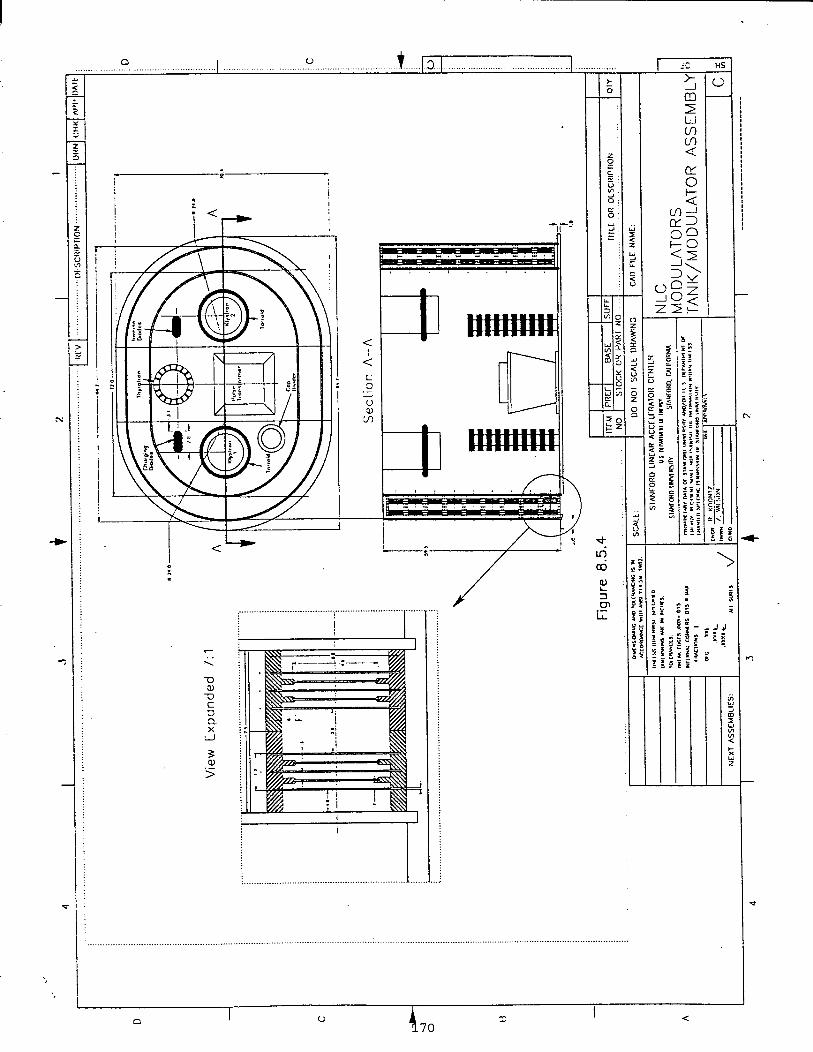
oI
v t. .......]..3..1 . . ....................1
I
1
!>
I-
II N n 1 T 8
i
. .\
J
/
. ....... .. ... .. .. ... . .
. .. . . ... . . . ... . . .. . . . .
*
,..

Concentric Plug–in 3–GapThyratron
171

8.5. Klystron pulse Modulator: (R. Koontz, s. Gold)
The Wystron Pulse Mtiulator is the pnncipd electronic system of the RF station.Fig. 8.5.1 shows a block diagram of the RF Station. The RF station con~ins thefollowing subsystems:
1.2.3.4.5.67.
~W, ]evel RF ~ontro]s and monitors Section 8.7.)
~ watt to 1 kW Hystron or TWT RF Driver (Section 8.6.4.)Dual PPM fmused ~ to 75 MW tiystrons (Section 8.4)A single thymtron Blumlein modulator driving two Nystrons (Section 8.5.2.)The modulator power supply (Section 8.5,3)The modulator, Nystron, and structure monitor& protection system (Section 8.6.)The Station cooling system and oil circulation (Section 8.5.4)
Sections 8,5 and 8.6 are discussed in detail below. ‘~
.’,,
,-..%..
172

! .
8.5.1. Modulator Requirements (P. Wilson)
.
..
Specifiwtions for the NLC modulator are given in Table 8.5.2. These specifications aredriven by the requirements of the NLC Nystron, as listed in the first seven rows of thetable. Although the initird design gord for this Nystron is an output power of 50 MW, =required by the ~ GeV NLC design, an improvement program is in progress which willeventually incr=e the power output to the 72 MW required for the 1TeV upgrade. Themodulator must therefore be upable of driving two Mystron at this higher power level.The repetition rate for the initial 500 GeV NLC design is 180 ~. To save AC power,this drops to 120 Hz for the find 1TeV machine. However, during the transition to thehigher energy, there may be a mix of 50 MW and 72 MW tiystons on the linac, opratingat 180 Hz. In fact, the higher power tube maybe available even at the time constructionbegins on the 500 GeV collider. In any we the modulator must be capable of driving thehigher-power tube at the 180 Hz repetition rate.
The first column in Table 8.5.2 lists the design goals for the 72 MW NLC tiystron, and acorresponding set of parameters for a modulator capable of driving two such Nystrons.However, as mentioned above, both tiystron and modulator must be capable of operatingat a 180 Hz repetition rate, as reflected in the second column of Table 8.5.12. Also, theNystron efficiency may fdl short of the ~\% efficiency,goal,”at least initially. To beconservative, the modulator parameters have therefore been chosen so that it m drive aMystron with an efficiency as low as 50\% to the required 72 MW output power.
A key consideration for a modulator in a linw collider application is the efficiency withwhich power is transferred from the AC line to tiystron beam power in flat-top portion ofthe high vol~ge output pulse. A 1% decrease in efficiency at any point in this efficiencychain resulk in an increase by between one and two megall)atts in the AC line power forthe NLC W system. An impo~nt component in this efficiency is the ratio of the usefulenergy in the flat-top portion of the pulse to the tod pulse energy, including the energyin the rise and fall-time portions of the pulse. This rise/fall energy efficiency is given(very roughly) by Tk Uk + 1.1 T@, where Tk is the flat-top pulse width and T@ is therise time (the constant 1.1 depends on the precise definition of rise time). In turn, it iswell known that the rise time is determind primarily by the turns ration n of the pulsetransformer (very roughly, TR is proportional to the turns ratio and to the square root ofthe pulse length). However, a low transformer turns ratio implies a high value for thecharging voltage for the pulse forming net~{’ork(PFN) or pulse forming line (PFL), and acorrespondingly high hold-off voltage for the thyratron and other high voltagecomponents. For a modulator using a stidard PFN design which can deliver a 500 kVoutput pulse this charging vol~ge would ~ shut 150 kv for the 7:1 transformer turnsratio listed in Table 8.5.2. However, by going to a Blumlein type of PFN, the chargingvoltage can be reduced by a factor of h~o to shut 72 kV. Although a Blumlein PFNdesign is somewhat more complex, it rn~es pssible both a low transformer turns ratioand a reasonable value for the charging volbge.
In a shndard modulator design with output pulse lengths longer than a microsecond or so,lumped elements (capacitors and inductors) are used for the pulse forming network. Sucha lumped network has the advantage that it w be readily tuned to adjust the pulse shape,although it is still difficult to elimina~ dl of the ripples to attain a truly flat pulse utiess avery large number of elements are used. Also, it is difficult and expensive to
‘, ‘,
173

1. . ., .
9
manufacture pulse capacitors with a vev low series inductance and long life, especirdly
when the polarity must reverse during the pulse, as r~uired by the Blumlein
configuration. For these r=ons, the use of lengths of smooth transmission line is beingproposed for the NC modulator. The major disadvantage of such lines (long length) abe ameliorated by choosing an appropriate patting geometry and good mechatic~design (see Sec. 8.5.2)
The riselfall-time energy efficiency, just discussed, is the major component whichdetermines the over-di modulator efficiency. In addition, a voltage drop across thethyratron and eddy currents in the pulse transformer core lead to an additiond energy lossof about 3 ~0. The charging voluge on the Pm must be about 1-l/2~0 higher tommpensate for these losses. The corresponding loss efficiency (W~o), multiplid by therise/fall efficiency, gives the net efficiency with which energy stored in the capacitance ofthe Pm is transferred through the pulse transformer into the useful flat-top portion of theoutput pulse. A detailed discussion the projected efficiency for the NC modulatordesign is given in Sec. 8.5.$5
174

I
Table 8.5.2
Klystron - Modulator Specifications
@wo klystrons per modulator)
Description: DwiW Dsi~Gnd M-n
~ystron Output Power (m 72 70 Min
~ystron MicropeNeance @perv) .0.6 0.65 Max
~ystron RF Pulse Width (~sec) 1.20 1.20
Kystron Pulse Voltage (kV) @o 517 Max
Mystron Re~tition Rate (Pm 120 1~ Max
~ystron RF Pulse Natness ( %) 1 1.2 Max
~ystron ~ficiency (%) 60 50 Min
Modulator Type: Distributed Network Blumlein with(drives two Nystrons) individud capacitor charger power supply.
Distributed Pulse Forming Net\\rork Vol~ge (kV) 72 75 Max
Rise/Fall time (nanoseconds) 3W ~ Max
PFN energy storage 2 Hystrons (J) 360 461 Max
Auxiliary AC Power Input (kW) 1.5 2.5 Max
(Thyratron heater, reservoir, control)
‘.
I
Avg. AC Input Power (kW) 50 460 Max
Pm (Hz) 120 lWMax
mat Top Pulse Width @see) 1.2 1.2
Output pulse voltage (kV) 40 505 Max
Output pulse current (M) (2 Hystrons) 430 Max
filse transformer ratio %-1 g: ~.
Thyratron pulsecilrrent (~) 6.0 6.5 Max6
/,“.
175

-
,t.’,.
.—-.
? ‘-.-1
.*
I. EOLC
12 OHM Parallel Plate Une 12 OhM Porcllel Plate tine —
1“
(7:1)
1’
D@mm
‘, .
176

A proposed modulator tank supporting two tiystrons is shown in Fig. 8.5.4. The pdlelplate transmissions lines are shown mounted in the space between the inner oil tank, andthe outer containment tank. The to~ length of ttis double transmission line assembly isabout ~ feet. The oil is mntained in a polypropylene racetrack shaped tank that dsoserves as the support for the transmission line assembly. The transmission line assemblyconsists of continuous aluminum strips supported by moldd nylon support insulatorsapproximately one inch thick spaced at 12 inch intervals. This construction allows myservicing and repair of the pulse line if an arc destroys one of the support insulators. Bysupporting the parallel plates from the end of the aluminum strips, the creepage pathbetween the plates mn be made long enough to prevent discharge while still keeping theplate to plate gap small enough to take advantage of the 20 kV+ per tenth inch breakdownproperties of the oil.
There are a number of secondary elements also housed in the modulator tank: the end+f-line clipper diode stack, the charging diode (if one is used), the current viewingtransformers and volwge viewing capacity divider, the core reset inductor, and thethyratron inverse clipper diode. All of these elements are contained in the inner tankadjacent to the thyratron and pulse transformer.
A double rack enclosure adjacent to the moddator unk contains all the supportelectronics for the mdulator, and the M drive electronics. The support electronicsincludes: the Nystron cathode heater supply, the thyratron athode supply, the thyratronreservoir supply, the control pwer distribution, the RF low level driver and interlocksystem, the one kW Hystron input dril)er (a special small Uystron or TWT), and a customdesigned PLC (programmable logic controller) that provides the control and monitorfunctions for both the pulse modulator and the Nystron RF drive and protection systems.
8.5.3. ChargingPowerSupplyDesignOutline (L. Genova)
8.5.3.1 Specifications(5W GeV Operation)
Charging VoltagePulse Forming Line CapacitanceJoules/pulse, 2 tiystronsRepetition RateCharging Voltage RegulationAC LineAC Line StabilityPower Supply Hficiency
72 kVO.124pF (PFL)320180 PPS at 500 GeV
(0.1%)40 V,3 phase, ~~3%B%
8.5.3.2 ConventionalChargingSystem
Traditionally, the power supply that charges the PFL ~pacitance consists of an AC toDC power supply, a filter capacitor bank, a charging choke, a charging diode or acommand charging SCR circuit, and a DQing circuit that regulates the Pm chargingvol~ge (See Fig 8.5,5)
177

\c[NE T +
POWERSUPPLY
1
*
DOlNG COMMANDu CIRCUIT ---— -—
.—
--C~fi~~~NG
TFILTER REGULATOR VOLT
CAPACITOR CIRCUIT SENSING+
J}
FIG.8.5.5 CONVENTIONAL PFN CHARGING PS
CHARGING
T I t
AC
d
~ POWER
.INESUPPLY
DIODES
CHARGING
FILTER CHOKE
TCAPACITOR47
# -11 I A
11’14 + I
i -h~>
FIG. 8.5.6 HYBRID CIRCUITCONVENTIONAL PS
CONSISTINGAND SMALL
OFCAP9CITOR
TOPFN
—
CHARGING SWITCHING PS (CCSPS) IN PARALLEL
GcLINE
+
CCSPSVOLT To
SENSING PFN
FIG.8.5.7 CAPACITOR CHARGING SWITCHINGPOWER SUPPLY (CCSPS) SCHEME

If we resume an AC line s~bility of (3%, then we must DQ at least 6% to meet theregulation parameter. If the DQing power is dissipated, the efficiency of the powersupply charging system is diminished. An energy recovery scheme could be develo~to recover the energy and feed it back to the power lines, but it would be expensive andwould ody recover a portion of the energy. With energy recovery, we could odyachieve a total power supply efficiency of 9070.
8.5.3.3 Hybrid ChargingSystem
A betier scheme would be to use a small capacitor charging switching power supply inparallel with the charging choke output (Fig 8.5.6 At the lowest line voltage, the Pmwould then be charged to 9470 of its peak voltage by the charging choke, and theswitching power supply would be used to charge the final 670 of the voltage, What wehave done is substitute an additive process for a subtractive one with a resulting incrwein efficiency. With this additive scheme, power supply efficiency could be as high as93%.
8.5.3.4 Capacitor ChargingSwitchingPowerSupplySystem
An even more attractive idea is to use a mpacitor charging switching power supply(CCSPS) to charge the Pm directly (Fig 8.5.7) The charging cycle starts with the Pmcapacitor at zero volts. The CCSPS starts charging the P= at constant current until thedesired voltage is reached. At that time the supply becomes a constant-voltage powersupply and keeps the Pm charged at the desired value. The charging wavefom lookslike a linear ramp which flattens out at the desired voltage.
--
The CCSPS supplies are becoming commercially available now and will be morecommon in the near future. A single 50 kW power supply is presently available whichwill charge the Pm to 50 kV at 120 PPS, will tolerate a voltage reversal of 2070, and hasan efficiency of 9390. Research is required to increase the charging voltage to aminimum value of 72 kV. In order to be able to charge at 180 PPS, two CCSPSS,operated in parallel using master/slave connections, are required.
This solution greatly simplifies the charging circuit topology since there is no need for afilter capacitor bank, charging choke, command charging circuit and high voltageblocking SCR strings. The elimination of the filter capacitor bank reduces the amount ofenergy stomge and the possibility of thyratron damage in a latch-up condition. With afilter capacitor bank, a false trigger or a thyratron br=kdown will cause the filter bank todischarge completely through the thyratron and then the power supply will short circuiti~elf through the thyratron. With the CCSPS, a thyratron breakdown would only resultin a maximum current equal to the nominal charging current since the CCSPS reverts toconstant current operation when it is short circuited. In addition, the CCSPS is muchmore compact than a conventional po~’er supply. For example, the w kW supply cited israck mountable, 19” wide, 22” deep, and ody 12.25” high.
Since we are planning to connect many pwer supplies across the same AC lines (480V,3 phme, 60 Hz), it is impo~t that the power factor b as close to one as possible. The
179

rated power factor of the CCSPS is 0.9. There is a need to add power factor correction
circuitry to increase it to at l-t 0.98.
8.5.4. Stition Cooling Systemand OflCticulation(R. Koontz)
There are several cooling circuits that remove hat from the Hystron and modulator. TheNystron hm just one cwling circuit that is a combination of all the passages on thepassages on the Uystron. Temperature monitor points on parts of the ~ystron (My,ande, collector, etc.) provide interlocking for over temperature conditions. Themodulator contains two oil systems, one for the transmission lines oil which may have ahigher dielectric than the main tik, and the other for the low dielectic oil for theHystron guns, the thyratron, the EOLC and charging diodes, and the pulse transformer.=ch of these systems will have a small oil circulation pump and an oil to water hatexchanger appropriately interlocked.
There is no cooling required in the RF system sup~rt racks unless the charging po~versupply is mounted in these racks and it needs water cooling, but there may be a need forwater temperature stabiliution if RF components mot be designed phase stable withtemperature changes.
8.5.5. Modulator/ ChargingPowerSupplyEfficiencyProjections:
At the time of MS writing, the efficiencies of the lrarious components and sub-systemsare being analyzed, but there are no definitive efficiency projections available as yet.The numbers will become clearer x R&D progresses.
.
8. 5.6 PFN / Pulse Transformer NeWorkSimulations
There have been several preliminary SPICE net~~ork simulations run to date whichshow the generrd waveshaps on the Blumlein as shown in Fig. 8.5.3. More detailedsimulations are planned to look at walreshapes using more detailed equivalent circuitsthat approximate red lines and pulse transformers. All the secondary parameters such asNystron stray capacity, the real characteristics of the various diode stacks and motitorelements, and the actual characteristic of a s~~itched thymtron will be added to the modelto get a better picture of what the rd pulse response will be.
The dielectric cons~nt of tie various normal and high dielectric oils must becharacterized as a function of frequency including dielectric losses as the propagation ofthe wavefront on the lines will k limited by these parameters. Mgh frequency losseslimit the wavefront rise time, and dielectic consmnt variations with frequency an smearout the rise time, and cause pulse overshoot if all frequency components of the \vavefrontdo not arn~e at the end of the line at the proper times. It will ~ke a little bit ofdevelopment work with a simulation progmm to allow the dielectric constant to have areal and imaginary part corresponding to loss and propagation velocity,
‘, .,
180

. .
-
8.5.7 Etisting prototypemodulatorperformance
At the present time, there is very litie experiment data to check design ideas. In the~ystron Test Ub, there are two modulators which can give some experiment checkpoints to simulations. Test Stand 13 is a high power conventional modulator whichcontains close coupled Pm’s and a direct connection to a 23:1 pulse transformer. Itprduces ~ kV pulses driving a pervan~ 2 Hystron for a 3 psecond flat top pulse.
Test Stand 3 contains a 1.5:1 Pm they mtiulator driving a 6:1 pulse transformer withdl elements in one large oil tank. It dso is designed to produce ~ kV pulses, but it hasnot run at full voltage in oil as yet. The capacitors that makeup the three P~’s thatconstitute the Blumlein have too much series intemd inductance to allow a very fast risetime, flat top pulse. Additional testing will be done on this modulator to get better dab.This test stand will be used as the location of new R&D work on distributed pulse linemodulators.
8. 5.8 Modulator/ PowerSupplyR&DDevelopment
& the paper desire of a possibleMC modtiatir evolves, the R&D areaswhere the new ideas must be tested start to surface. At the present time, wecan divide the R&D effort into two categories, component and subsystemdevelopment, and system concept testing.
‘.‘
In the component and subsystem area, R&D programs are needed b developthe oil immersed parallel plate ptise Enes, a new thee gap thyratron that islong life and easy to manufacture, the whole general field of ptisetransformers bcluding manufacturing cost minimization, economical andrugged diode stacks, a new pdse charger for this application, and the generalsimpltication and cost opttiization of the support electronics.
For system concept testing, a parallel plate transmission must be constructedand tested to prove the principal. This can be done ushg the various ptisedenergy facilities of the ~ystron Test Lab.
‘,’,
181 .

8.6. W Unit Protection, Monitor, and Drive Systems
Protation systems are rdl servicti by the PLC plus some additionrd faster protectioncircuitry. This pro~ction system combines the logid protection and operating functionsof the modulator, the Nystron, and the waveguide and structure systems. It includes thewater cooling system, the temperature monitoring system, the various electronic monitorsof the Wystron supprt power supplies and the modulator electronics, the related vacuumsystems, and the high power RF protection. While dl of these various protection andinterlock systems are serviced by one PLC, the functions will be discussed separately inthe sections below.
Much of the monitor system is part of the protection system in that if monitoring isnecessary, it is probably because some protection interlock is essential to the safety of thesystem. Because of the large number of RF stations, monitors that provide informationinto the general linac operating system must be kept to an absolute minimum to limitcosts.
fich RF system has associated with it a Mystron RF drive package that consists ofsome low level RF processing and phase programming to make the SLED compressionoperational, some RF interlocks, and a kilowatt driver to provide inpu~to the Hystron. Inthis section, the RF interlmks are discussed, and the kilowatt driver. The other low levelRF processing is covered in Section 8.7.
8.6.1. W Monitor& ProtectionSystem
RF Structures: Stmcture protection includes all of the high power X-band waveguide,the SLD 11energy compressors, and the disc loaded waveguide. Other than acceleratedelectron beam interception damage over which this interlock system has no control, theprimary causes of potential component damage are arcing brought on by poor vacuumand loss of cooling. Because of the limited pumping sped of small waveguide, the highpower RF distribution system contains many individud ion pumps. It is expected thatthese ion pumps will be serviced by a small number of multiple output ion pump powersupplies that will be interlocked with the RF system module.
There will be a limited number of reflected energy pickup points, especially in the outputarms of the Nystrons that will detect reflected energy due to arcs or SLED 11mistuning,and will operate through the PLC to inhibiHystron pulse modulator.
either the drive RF to the Mystron, or the -
Klystrons: Mystron protection is accomplished by providing monitoring and interlockson the systems which provide power and cooling water to the ~ystron, the ~ystron
.,.,
182
..-..=%,

I..
.:-vacuum and the RF systems including the system vacuum. These monitoring andinterlock signals are both analog and digiti.
Most of the interlocking is done through the use of a Programmable Logic Controller(PLC) which provides the interlocking and sequencing logic for the Nystron system.H control and human interface for status r=dout is planned as a touch screen panel.Critid interlocks such as ~ystron Output Reflectd Power, which require fasterresponse time, are also direct, hard wird.
The water system is designed for two Mystrons pr station with separate water circuits foreach Mystron. Each tiystron will have a water circuit for its anode, ih body and windowand its collector. The separate water lines will be protected for minimum flow by a flowswitch. The flow switch dso puts out a signal which an be used to read flow. Thiswater manifold will provide the cooling water for the ~ystron/ modulator oil tank and itwill also have a flow switch for minimum flow protection. A summary water interlmkfrom the PLC will signal the main computer system of the failure.
Each ~ystron is separately instrumented for window temperature and body deltatemperature. The body delta temperature, which increases if beam interception incrmes,is fed to the PLC compared to a pre-determined level. Exceeding this level causes thePLC to turn off the ~ystron &am. Window temperature, also read by the PLC as ananalog signal will cause the RF drive to be removed if a maximum temperature isexceeded. The main computer can interrogate the PLC through a communication linkand read the interlock status and window temperature.
.>
The Nystron Vacion pumps will be padleled into two Vacion controllers for eachUystron. The controllers will have an internal vacuum pressure limit interlock which willbe manually set. An excessive vacuum pressure interlock will turn off the Nystron bmthrough the PLC. A vacuum fault indication will be sent to the main computer system.
The Wystron heater circuit, separate for each ~ystron, is equipped with an interlock forminimum heater current and a warm-up time delay is provided by the PLC once theminimum current is exceeded. ~ystron beam is inhibited until these interlocks arecleared. Analog signals for heater voltage and current are read by the PLC andtransferred to the main computer system via the communication link.
~ystron peak ~thode voltage and peak cathode current are digitized in the Wystron andModulator Support Electronics and read into the PLC for Overcunent and Overvoltageinterlocking and into the main computer system for data taking and storage. TheHystron and Modulator SUpPrt Electronics includes the circuitry and connectors toattach a PC, running LabVIEW, for special data taking during diagnosis and analysis.This system can be easily configured to look at any of the analog and digital signals, for astation, on a vev frequent time s~le, record and visually present the data.
~ystron Heater and High Voltage operating hours will be totaled in the PLC.
The W Output waveguide transport system, ~vhich is under vacuum, contains Vacionpump supplies with mmudly set high vacuum pressure interlocks. These feed into themodulator and ~ystron PLC to remove RF drive for an excess pressure condition.
.,‘,
183

The ~ Output waveguide transport system also has various forward and refl=tedmonitor points. An example of one of these monitor points is at the output of thetiystron. These signals are =ch shipped through a four port coupler. One of these prtsfeeds a CWSM detector into a Video Amplifier system which provides buffered videooutpu~, a-peak and hold detectd output-and a ~mparitor circuit. The comparatorcircuits with manual adjustment can be usd to interlock any of these detatti signrds.The output of the interlock is sent to the PLC for action. ~ystron reflectd power is oneof the critid interlocks which will dso be hard wired from the Video Amplifier interlockto directly remove M drive.
8.6.2. Modulator& SupportElectronicsSensing&Prot~tionThe mdulator control, sequencing and protection is dso accomplished through the PLC.The main protection interlocks are excessive bd of Line Clipper (EOLC) current (for aMystron arc) and High Voltage Power Supply Overcunent (HVOC). The modulator ldinterface is also through the Touch Screen Panel.
The modulator protection system contains discharge solenoids, barriers and doorinterlocks for protection of both personnel and equipment. It is connected into the overallaccelerator Personal Prokction System (PPS). ‘, .5
..- -.
Thyratron warm-up time delay will be started in the PLC after the thyratron electrodes are
.
energized. Thyratron heater hours will dso be totied in the PLC. “
8.6.3. The Klystron/Modulator Logic Controller
At the present time, PLC’S are being used for monitor and interlock functions in theWystron Test Lab. On the NLCTA, two PLC’S are used at each Nystron station toprovide modulator interlocking and control, and to monitor the operation of the tiystron~ system and the various interlocks that protect the W station. It is expected to usethis same technology for the NLC ~ station, but the general PLC will be replaced by adedicated logic controller that is designed and optimized for NLC ~ station operation.
8.6.4. The Klystron W Driver (TW or smallKlystron)
There are various schemes for providing the approximately 1 kW of pulsed ~ that is thedrive source for ach high power Uystron. It is useful to have individual drivers as thevarious phase manipulations that go into the operation of the W compressors are bestdone at milliwatt level. Power programming of the two Hystrons on the single modulatoris done by differential phase modulating the two ~ystron inputs which has the effect ofsteering the power summation either into a dummy load or the ~ pulse compressor.
There exists extensive TWT technology at this frequency and power level as a product ofmilitary applications. The available TWT’S are reliable, but fairly complex tomanufacture and operate. They have already been pretty extensively cost optimized, andare still very expensive.
.,‘,
184
I .,-. . .-
A small x-band tiystron design of fairly narrow bandtvidth and gain is not too difficult todesign and build. In cons~ction, it is relatively simple compared to a T~. It ispossible that after the initial engineering models are tested, a modest program of redesignfor automatic manufacturing could reduce the unit cost to something approximatingmicrowave oven power source sale. A little arly R&D effofi in this area would kuseful.
8.6.5. Monitor& ControlElectronicInterfaces
Almost all of the monitor and control for the RF station can be handled with a loiv datarate interface between the station logic controller and the central computer. There are afew signals that require fast response including some diagnostics, but with 4,~ RFs~tions in the NLC system, fast, broad band dau retrieval will be very limited. More onthis interface subject vrill be written as the system develops.
...
.,
185

!.
~ystron Development Overview, NLC ZDR
EsotericDesigns:
NLC ZDRModulator
Gridded~ystrons, HardStitch Tubes,Quasimodulators,HighVoltageStitchingandotherideasneedingmajordevelopment
ZDR (Zero DesignReport)Modulatormakinguseof efistingandshorttermdevelopmenttechnology.
,.
186

Modulator Developmentin Future -
~ S- B*ess (SBR’S)New good id- lowcostdev~opment
N. Maintie, ~gh VolumeManufac-rsmot representedhere)-pies Auti kd~ Gened Moto~ Fofi
~h volumeelectronic%~~ Appl%PattiBe~ eti~ectric Powerkd~, Westingho~ GE,?
187

Modulator Developmentin Future -
The Charge:
Get started on serious R&DonComponents
Evaluate and settle on base modulatordesign
Get prototype(s) built - running - evaluateand optimize efficiency
Re-engineer for minimum cost, maximumreliability large volume construction
Watch for breakthroughs in klystron andmodulator design concepts that couldimprove efficiency, reliability, and reducecost.
188

RECENT PERFORMANCE OF KLYSTRON TESTING MODUMTO~ IN ~E SLAC KLYSTRON TEST LAB*
R. F. Koontz, S. Gold, J. EichnerStanford Linear Accelerator Center, Stanford University, Stanford, CA 94309
Abstract
me tix of Hystrons being designed and operatedin the SLAC Mystzon Test bb continues to expandand now includes large klystrons, CW and pulsed,from UHF to X-bad. To support these developments,a number of new pulse modulators and power supplieswere desi~ed from scratch, or upgraded from existtiglaboratory test systems. This paper presents recentexperimental performance of these modulators mddescribes a quasi-line power supply that couldefficiently support a high-power gridded klystronwith a special isolated collector.
400 MW Peak Power Moddator (DESW
A 400 .MW peak power modulator was designedand constructed to power and test a 150 MW $Bmdklystron for DESY. The basic approach, firstdescribed at PAC .93, is a straightfomard SLACmodulator except that four parallel lines and twothyramns are u~ to obtain ~e low Ike impedanceand high discharge current. The voltage is obtainedby using a pulse transformer with a turns ratio of 23 to1: A s~pl;fied schematic of the moddator is shownin Fig. 1.
Specific attention was paid to minimizinginductice in the primary current path. ~s stray orwiring inductance- and ~e pulse transformer leakageinductance are the limiting factors in the outputvoltage rise time. Therefore the connection from thePFN ~o the pulse transformer was made using &inch
FE~‘‘...
cl-w .W4 @
L...
w xv nmti
L14@ 1.3@
. . . & 1.3 n (tot@
. . .
. . .
@
L...
. . .SW KV W
L..*1.8
=3SkVIn
Q 3m
--- -0 0
tip 4;’4
I1=
7UMI
Fig. 1. Simplified schematic 550 kV moddator.
‘Work supporti by Department of Energy contract DE-ACO>76SFO0515.
parallel-plate copper bus and kept as short aspractical by directly coMecting the pulse tank to thePFN cabinet. Connections from the PFN to thethyratrons are copper tubing. The four ten-sectionPFNs are packaged in a sbgle rack with hdf of thecoils on one side and half on the other producing acompact, symmetrical assembly. The thyratrons arelocated on either side of the PFN and the ouput tothe pulse transformer is beween the thyratrons.
Earlier this year the modulator was brought intooperation and used to test and process a beam diode to550 kV, 700 amps, 3.5 W, and 60 Hz PRF. Figure 2shows the beam voltage and current waveshapesobtained with this diode load. The peak beamvoltage in this waveshape is 532 kV, and the currentis 673 amps peak The rise time of the beam voltagepulse is 0.8 ps from 1070 to 90Y0. ~is measured risetime compares with the simulated 0.7 ps rise time forthe pulse transformer and a primary estimated leadinductance of 03 @. Figure 2 also shows the primaryrise time of the PFN-thyratron combimtion to be veryfast, less than 80 ns. Even with Mls fast rise time anda primary discharge of over 15 klloamps, the ringingis minimized because of the close coupling of themodulator elements and the minimum-inductance,tinirnum-stiay capacitance design.
200 MW Peak Power Simple Moddator
Another modulator, which we like to call“conventional”, was constructed in the Hystron TestLab this last year to power m X-band Mystron thatdrives a resonant ring. ~is compact design is capable
?1, r / “
j~ ~ 1 f[
\& ~wm curr~t = j7M
—
&a4 1~sddiv ~Fig. 2. 400 MW modulator voltage and current
waveshapes.
189
Presenti at tie 1W4 kkrnatioti Linac Cotiereme
Tsukuba, Japan, AuWst 21-26, lW
of driving any Hystron from 350 kV to 430 kV at aperveance from 1.2 to 1.9 pperv. The pulse width canbe adjusted from 1 w to 4 w by selecting the number ofPFN segments in the network. The pulse capacitorsare 0.044 pfd, 50 kV each, and the tunable inductorsare 2 VH each. A standard ~ 241 thyratron is usedfor the switch element or the corresponding EEV, orLitton tiyratrom may dso be used.
tie and 3 MW CW Test Stands (B Factory)
CW low-frequency klystrons are being producedand tested in tie Klystron Test bboratory for use onthe B Factory. At present, there is one SW kW, 476MHz klystron k place on tie one megawatt test standthat is used for component testing. The power supplyin this test stand operates at 67 kV, 15 amps. A second,higher voltage and power test stand is underconstruction that will deliver 97 kV, 30 amps to a newdesign 1.1 MW CW 476 MHz Hystron. The powersupply is designed to provide three intermediatestages of voltage that can be used to bias a depressedcollector for energy recovery. The test stand isinstrumented to operate a depressed collectorklystron, although a depressed collector klystron isstill in the preliminary design stage. The 3-MW teststand uses a programmable logic controller (PLC) forthe interlock system. The test stand will be inoperation in December 1994.
Quasi-1ine Power Supply for Gridded Wystron tithIsolated Collector
Because of the vev large rf power demand of allproposed NLC systems, it is most important tomaximize the efficiency of rf delivery systems.Ener~ is dissipa~ when large amomts of charge aremoved into and out of the system stray capacities. kaddition, the klystron electron beam dissipatesenergy during the rise and fall times of the beam pulsewhen no rf energy is produced. As Uyshon voltages gohigher, and pulse widths grow shorter, there ispressure to build faster and faster rise- and fall-timepulse modulators to minimize these losses. The fastrise and fall times, however, do not change the energylost in charging stray capacity, or left over in strayinductmce. This energy is lost independent of thepulsed power rise and f~ times.
It has been recognized for some time that thecathode of a klystron need not be moved in voltage ifthere were some other way to control the currentemitted from the cathode. Some klystrons at lowpower have been built using either full or partialvoltage-swing moddating anodes. These designs limitthe amount of stray capacity that must be moved toproduce pulses, but the voltage swing necessary to
switch on current is high, and the cathode voltagemust come from a DC supply that contains much storedenergy. The gun area of the Mystron must be desiqedto withstand his DC voltage without arcing, and arcprotection in the form of a high power crowbar must beincorporated in the des[gn to discharge the highstored energy of the DC supply. Until now,conventional wisdom has dictated that high power,short pulse Mystrons be built with diode guns drivenby pulse modulators, usually tine type with step-uppulse transformers.
It is time to revisit the idea of high-voltagegridded guns for Hystrons. New cathode technologythat allows emission at a lower tempera~re makespossible the use of a conventional intercepting grid infront of a klystron cathode that can have atransconductance approaching 50,000 ymhos. Thiswill allow the Mystron beam to be switched by a fastgridpulser of ody about 5,000 volts. Such pulsers areavailable in solid-state componenb with rise times ofless than 5 ns. The beam optics of such a Mystron gun isdifficult, but not impossible. A serious problem,however, is the DC voltage holdoff, and theminimum stored energy required in the DC supply todeliver the klystron beam current without excessivecathode voltage droop.
To make a high-voltage, fast-grid pulsedklystron feasible, a limited energy storage, highvoltage pulse line can be used with a speciallydesigned Mystron incorporating an isolated couector.Figure 3 shows a block diagram of a unique quasi-linepower supply-klystron system that is almost circuitloss free. For this example, a klystron of lowperveance (0.6 yperv), high voltage (500 kV) isswitched with a 5 ns rise and fail-time grid drivepulse (1.5 w pulse duration). The Mystron cathode isconnected to one terminal of a high-voltage lumpedelement PFN, which in this example has acharacteristic impedance of 500 ohms. The unique partof this design is that the other end of the PFN isconnected to the isolated collector of the klystron.Note that this configuration allows the Mystroncathode to be held at a fixed 500 kV potential by alow current sustaining power supply which can dso beused to maintain intermediate voltages on the multi-element DC klystron gun. h operation, this sustainersupply delivers ody the klystron cathode currentthat is lost to the Uystron body.
The uniqueness of this design is the voltage swingon the Uystron collector. Assume that the PFN hasbeen resonantly charged to 600 kV from anunregulated, multiphase 500 kV power supply with nocapacitor energy storage. There is 500 kV across thecathode-body gap, and this voltage is held fixed bythe sustainer power supply. With no beam in theklystron, the voltage that is present across the
190

Ca
*t T;00 w
ode-500 w I
1
$(b)
Cathode VoltageRegulator
n Beam 1>11Grid Impedance RF
Pulser 2,500Q ~tive On;utFig. 3. @asi-ltie Nystronand ~wer suwly system.
klystron collector-body gap is +lM kV. The gridpulser now turns on the Mystron cathode to 2~ amps.The PFN sees a real beam load of 2~ ohms be~eenthe klystron cathode and collector. This 2* beamload on the PFN reduces the PFN voltage to ~ kVwhere it stays for one discharge period of the PFN.The voltage on the Uystron couector goes to zero witirespect to the klystron body. At the end of onedischarge period of the PFN, the grid drive is turnedoff, the beam current stops, and the voltage on thePFN drops to 4~ kV. This applies a -1~ kV voltageto the klystron collector. The resonant rechargereturns the PFN to 6M kV over the interpulserecharge period, and the Mystron is ready to pulseagain.
This system design allows a W-grid pulsed gun tobe mated to a mismatched high-voltage PFN oflimited energy storage without the gun having towithstand the overvoltage of a charged PFN. Theover and under voltage swing has been transferred tothe collector of the klystron. During the actualMystron beam pulse, the voltage on the collector iszero, or dose to zero. The “close to zero” statement isimportant as the PFN network ripple md capacitivecharge and discharge voltage appear here during theklystron beam pulse rather than on the Mystroncathode. Within limits, these voltage variations atthe collector do not affect the beam efficiency of theklystron. The resonant charging of the PFN is selfregulating during normal operation, but on initialstartup some clang of the charging choke is necessaryto limit the initial inrush current from overvoltagingthe network.
Collector
The block diagram shows a capacitor stack, andan active makeup voltage regulator in the sustainerpower supply circuit. Skce the klystron body currentcan be as much as l% (2 amps) during the beam pulse,the capacitor stack is necessary to deliver thiscurrent. Low value capacitors are used in thiscapacitor stack to minimize energy storage, and anactive regulator is used in the bottom of the stack tomaintain and regulate the cathode voltage during theklystron beam pulse. ~termediate gun electrodes arealso fed from this stack, and the high impedancenature of the sustainer stack provides a measure of arcprotection for the gun. An arc between any twoelectrodes causes the voltage between these electrodesto collapse witi the lost voltage being distributedamong the other gaps. The arc extinguishes, and noenergy from the main PPN is dissipated in the arc.
This scheme of klystron power systemdevelopment rquires primary R&D work in Severalareas. A few are listed below.
1. Low temperature Uystron cathodes mated withhigh transconductance grid structures.
2. High voltage, compact, low lead inductancePFN’s operating in a common oil tank.
3. High vacuum low perveance, high voltagemultielement electron ~ with good beam optics.
4. Medium voltage holdoff isolated collectorswith low impedance rf choke joints.
5. Periodic, permanent magnet focused Mystrons.With much R&D and component development,
this type of high power rf delivery system has thepossibility of realizing the high efficiency needed fora future NLC accelerator.
191
.,.... .
192

%–1) *u=7Y7~~7%-? Table 2.3.1
General RF Desig~ Parameters for Main Ulnae
m
RF frequency (GH~
Accelerating Gradient
Unloaded/Loded (MV/m)
Active Unac Lengthl) (km)
Total Linac Lengthz) (km)
Peak Power per Meter (MW~m)
Stmcturm per Power UnitStructure length per PU (ml
Total Number of Power Units3)
Total Number of Klystrons
Total Number of Modulators)
Repetition Rate (Hz)
RF Pulse bn~ ~)P-k Beam Currents)(A)
Total Ave. RF Pwr. at Str. (MW)
TNLA
1.3
25/25
20
29
0.206
32
33.2
604
604
604
10
1315
.0083
54
SBLC
3.0
m30.2
33
u
i2517
2517
2517
50
&
0.30
51.6
11.4 11.4
y m14.2
10.3 15.6
~ a
4
A g
1804 1970
3608 3940
3608 1970
150 180
0.23
x 0.74
32.4 30.5
() <.
TBNLC
11.4
100/74
7.1
7.8
200
1
1.8
3938—
26
120
0.242s)
1.49
41
*
14
y
7.0
u
A1400
1400
140
300
SB
22
(!
1) Active length = [(5w GeV-2 X injection energy)/(loaded gradient)] X [factor for BNS damping and energy management],
2) Total linac length = Aclive Ienglb plus allowance for beam line componenb, including crymlat.
CLIC
30
80/786.3
9.4
144
20.56
11233—
2
2530/
1210
.0116 .
SB/1.9426.5
3) Numbcl of power uni~ = number or klystrons for TSSLA, SULCand VLEpP, = number of pulse compraion unib ror JLC and NLC, = number Ortransf
structura rot TBNLC and CLIC. For VLEPP there are two pulse cnmpr-ors per power unit.
4) Number of drive beam for TBNLC and CLIC ●nd number of high voltage murca (eupermod.lm) for VLEPP.
5) ~uivalenl length for ~ reclangulas pulse.
6) SD = 3in61e bunch -ccelcralion.
193

RF System Efficiencies and AC Power Requirement: Design Goals,, *
vTESLA SDLC JLC I N~C I TRNLC VLEPP CLIC
T70 .“50
2.4 “2.5— -
96 97
86 8D
.-.
60 92 60 75
1 — 1.4 —
77 — 74 —
94 98 95 90
72 44 95 55
3 3 0.4 1— — — 24
4 3 2 z
31 40 40 35
98 103 55 75
102 106 57 100
030 390
39 26
7,4 16.7 8.3 1.6/8.0
~cy 1)(W
Klystron Auxiliary Power2) (MW)
Power Transmission Eficiency (%)
}lodulator ~~~ 3) (y.
Modulator Auxili~y Power 4, (MW)
Cryogenic Power (MW)
Total Aux. plus Cryo. Power (MW)
RF System Efficiency Excluding
Auxiliuy & Cryogenic Power (%)
AC Power Exclu&ng Auxiliary
and Cryogenic Power (MW)Total AC Power [MW)
Net Eficieocy for Production
of RF Power$) (%)v
Efficiency for ~oversion of
RF Power to Beam Power (%)
45,. 7
98
95
8?
5—
58
62
3.5—
6 12
58 38 34
g4s) 133
1545) 139
35 37
102
114
03021 I 10.4 5.6
1) For TBNLC/CLIC:tMciency for conversionof drive bsam power 10 rf.
2) Csthode heakr plu denoid power.
3)
4)
5)
6)
Drive besrn produclbn cmciency for TBNLC/CLIC.
Thyrtiron calW -ad r-rvoir heater power (drive beamfocusingfor CLIC).
D= not include regulation r~rve.
lncludin~ cryogeaic power for TSSLA snd CLIC.
. .
Modulator Parameters: Design Goals and Ac~ieved to Date *
,NLCTESLA SBLC VLEPP
Modulator Typel) Storage cap.with bouncer
PFN Blumlein PFN Blumlein PFL Gridded Gun~
TDtiign Ach.’ds)
1.5
:;= 60
81 589725893 =9072 =521.5 1.5
Design Ach.’d D=ign Ach.’d
~ 3.065 43
1:1s 1:23
m a 65
~ 65
97 95
1000 1650
95 90
79.5 % 60
1.5 3
77.5 59
54.2 88
Flat Top Pulse Length, TL(PS)~TrangfomerxRise/Fall Enerw Effi~Scaled Ener~ Efficiencyz) (%)12R/Thy./@re bss Efficiency (%)Energy Stored on PFN3) (J)Power Supply Efficiency (%)Mod. Eff. without Aux. Power (%)Auxili~y Power4) (kW)N~)Ave. AC Input Power (kW)(Including Auxiliary Power)
131491:13
2010101:13
—
86
1000 ~
n 11
— —
— —
95
0.392.5 5m
99
86155
70m
I
1) PFN = lum~d &ment puk forming nclwork; PFL = PUI* fo[ming line (transmission tine).
2) Sss1..1.
i
II
3) Energy awitded pcr pulx from slorageelcmenl for THLA and VLEPP. ‘ JLC: x2 p(Al&4) lncludu lhyratron cathode heater, r-rvoir betler and other conlrol power.
“ ~K : X3 BI*U5) Sland~d (not Dlumlejn) PFN. 194

-H—
d% k[&
-><
.--A -—
b- 1
2.-v
‘m

“$—
I
II
1I
I
. -..’.
.. — -,

@..~& TV+..........“..: .,.&sf
,,,,...:

.LIOI-103=340nH.L201-213=3.40nH.
c] O1-112=2.9nFC201 -2 I2=2.911F
3
198

.;
199

200

—
/
201

.,.. ,. .-.
‘!’‘ ‘/l.!,:/lf,-- ,“’() ,1
: .:
‘.- ..————--- -- -————. —- ----. .. .
.,
202

0%
203

L.— —-—
I
204

205

—
.. . . .. .. ... ._...._. . . .. ..
206

4 COS*
207

u m > w u

Comparisons of SLAC Tubes
Item 5045 150MW DESY(1985)
Frequency (MHz) 2856 2856
Beam Voltage (kV) 350 475
Beam Current (A) 393 622
Perveance (u) 1.9 nom. 1.9
Max. Gun Gradient (kV) 201 208
Peak RF Power (MW) 65 150
Pulsewidth (us) 3.5 1
Rep Rate (Hz) 180 40
Average RF Power (kW) 43 6
Single Pulse RF Energy (J) 210 150
Tunnel Diameter (in.) 1.25 1.476
Efficiency (%) >40 50
Gain (dB) 50 nom. 59
Magnetic Field (Gauss) 1400 1800
3000
535
700
1.8
150
>150
3
50
27
>450
1.25
>40
>55
2100
209

m
f
zu
210

I ...
..
211

d
Q
u
212
.

t
o:I
I
I
I
I
IrI
I
t
I
I
I
I
, 1
!
II
I
I
t
t
I
I
I
I
t,
i
.
[
--
:
:
I
.
al I9-----.
*
1[ II
I.
1: n2u’

. . . ,—
I
I
I
,) .——d I; cx z
I.I.
I F/II ‘n
JI.
II
a
60t8’b0b
e.0b*..,0.‘e,.
●.,0*. ..0
09
QI
8I
7
214

.
.
. ...,,.,,
:
.● ✌
☛✚
).
.. . . . . . . .
. .
.
,
,.,,. ..,., .
.
.
*.
.
.,.●
●
✎ ✎
. .,,
[’n.. .
I...... .
!
!’
.,..
.
.1II
tti:”.
. . . . . . . . . b....$
. ./
. .
“i. ,*....+
●0 ‘ .0.:
.
.
.
r...Em . . . .
:. 8..
1:........4 ...,. . .
\
. 0,.,....... . . . . .... .,’. . . .,
,...
,.
.
T
. . . . . . . . . . . . . . . . . . . . . . . . . . . . . . . .
1. . . .
#. . ..
.
\
.“
..’. . . . . . . . . . ..
. . . ..
L...... . . . . . . . . . . . . . . . .. . . . . . . . . . . . . . . . . .
!“.
.

m Stoppw: 78 ~ukh~
[’”””
. 1—-.”........-.......-..._..-...-_”___:.. : i 1., ... .,,..... ,. .1,,.. ..I..Z= I
.+.
$::::v +.................. -+....................7
. . . . . . . . . . . . ... +
. .
. . . . . . . . . . . . . . .
+-+
-.j;{:::
... . . . . . . . . . . . . . . . .... .. ---- . . . . . . . . . . . . . . . . . . .,, .
. . . . ... . . . . . ., .,, ,,, ., ,, .,, . . . . ...
0 5.00Ms RLIIIS After.”
T* Stopped; S Acqliisitiol~sf---T------–--—— .-..-.... ;,. J.:. , ,;. , . ~“’’.”””~’~<’’.~< . . . . . . . . .
i.?
. . . . . . . . . . . . . . . . . . ..+-. ..:.”.”;”...:.”:’
. . . . . . . . . . . . . . . . . . . .
. . . . . . . . . . . . . . . . . . ..j. . . . . . . . . . . . . . . (. . . . . . . . ..
Cv( :
CU2 :
cq3 :
v -;.
+ j+-;-
. . . . . . . . . . . . . . . . . ..+..”............... .....:,’ .?
.>
2A(4;v
.

.
.
g/AS tZ kV
60mA
r ----
D
.
\
PULSER 80X GLASS
TaRNS FOUffEu F16RES
217

FAST HIGH VOLTAGE ~ANSISTOR SWITCHES
HTS 151 AMm 151mm 301Patent ~endin9.
IHTRODUC7XOR
Thesf suitches h?: been designed for nish VOlta$e,
high sDeEd suitchimg a9Diic8tions such as acclera-
tion- and defection grid drivers, oockels cell,--
drivers snd nanosecond Dulse Generators. aeceu$e oftheir siaDlc control and hioh voltsxse Stren$t”h, themodels HT$ 151 and HT$ 3$1 can be used as directreplacement for high volt- tti+s in namY s~itcbin~aDDiications. In cmftrost to tht conventional tubes,
HTS transistor svitcks ti not rwire heatixss Doveror high auiiii~y wilb- nd tihe live times arttvsical for sesicmductior Nims. Tlhe suitehes arecmstructed uith a w~lbi’tu~ d swdr-s control-led NOSFEis. Nich m hiqh~y il=llltied winst earthsd control circuit. Twmting-m uill be effected bya control si~l M 2 bo 110V@L’tsmlitadc. lheturn-on rise tim -s es=tially en the
oserating voltm, 4rw- md hoed c-tiitmces.Rise tiaes in the ortir of 110to 20 nmo-mds millbe achi!ved with ooti~ized cilrcua’t designs. S+causeof the 9*lvanic i,901+ation, oositive .as well as
negative volt-s can be witched on or off. Thesuitches aa~ be flloebed also at him oeteatials, ifthe sum of Vwking vo!bage and fl’oatim$ volta$e does
not excttd the sDecified isola!tiom strength.
CIUCU1lDESIGN COHSIDCRAIIOSS
3ifict Hij-suitches can sesxerate eatreaeiy raDid ratesof Vo!tase and current change. the circuit designshould be in accordanc~ &ith the troical reauireaentsof RF-circuits. That aeans &tl leads should be keDt asshort as Dossible, oart ~nents must be 10U induc-tance tyDes (No uircwound resistors!) and Douer suD-olies should be dmwied. 8s weil as ground leadsaust be connected as smt as oossible to a coaaonground Doint. Vhe w6e of shi~lded coaxial cables uithProDer terminatim is rccamded for the connectionof control iwut. To aveid electroaaonetic interferen-ces, the cooolete set-w -ld be olaced in a shiel-ded housiM. [f the circssit as not designed accordingto the above aantioned RF circuit orincioles, wildoscillations Md undefined watchins S*Y occur, Uhichcen cause a suitch overttiim, especially in case ofloads with 10U imedmnce6. Tokew the risk of Oscil-lations as 10U as o~scibte, a cmection between logicground and fiV-sroundis oftenfiet~s6ery.This connec-tion shouldbe keot verv short. FM this ouroose thereis a third terainfil at the H?-side of *odule, which isinternally connected uith tti logic ground. [n a floa-ting set-uo, the c~eeti~ of tti oround POintS uillbe Bade by ●e4ns of a cowling caoacitor Cc.
218
&hlkcElectronic Gmbl I POslfocll 190249 Telelon 0G9)733215 TIx 0402/6101602blI IuMalnzer Landstrafie 276 D.GOOOFrankluti 1 Telefax 069/733179 BIx 0697332150001+

. . . .W stopped: 132 Acquisitions
16 .
L. . . . i.. .-i-..” i....j....? . . ...”.”.. . .-.!.-..& . . . . ., 1r .Rn: +++........................~.......-
.1
&/l...................
:4. . :I
t . . . . ;.. . .,. . ..:. . . . . ... . . . . . . . . . . . . . . . . . . . . . ;, . . .
hl 2.00V%1
Ch2 500 mVQ M 50.Ops: Au%‘f OvD 1.00us Rum A~er..
~ 500mV 1.oops
Cua :
CHL:
Chl Pk–Pk1*VA03 w
Ch2 Pk-Pk
60. LA
C;;op:l
219
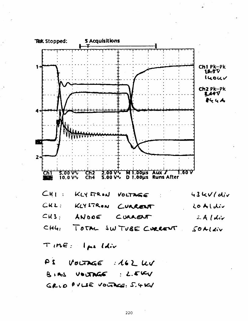
I.
!
* StopWd: s A~uisitbns8 j. . .n-+..i.’-. !..-”!... .“.”!...!. .’ i . . .
... 1::::
1
T..~ -A. . . . .
bw4.”:
. . . .
. . . . . . . . . . . . . . . . . . . .
. . . . . . . . . . . . . . . . . . ‘
1. . . . . . . . . . . . . . . . . . . . . . . . .
. . . . . . . . . . . . . . . . . .
. .
ch2 Pk-pk
e%QA
“P::: ‘:~2 :....:....t...:””..t
t+. . . . ;....;... .; . . . . ; . . . . . . . . . ; . . . . . . . . . ;. ...;... I
1 500 % 2 200V M1OO PS Au%I~ 10.0:% Q 5:00 ~; 0 l:OOMS Kuns ARer ●
160V
220

Conlnlissioning of tile Hard tibe Pulser Experinlent at DESY
M. Bieler, S. Choroba, J. Hameister, H.-Ch. Lewin,R. Giebeler*, S. Gold**
Deutsches Elektronen-Synchrotron DESY, Notkestr. Sj22603 Hamburg, Germany -
*Pri\’ate Consultant, ‘“On leave from SLAC
Abstract
The development of adequate modulators for high peakpower klystrons is one of the focus points for linear colliderR & D programs. For the DESY/THD S-band linear col-lider study 150MW rf-pulse power at 50Hz repetition rateand 3ps pulse duration is required [1]. Instead of the con-ventional method of discharging a pulse forming networkthrough a transformer to the klystron, a hard-tube pulser(HTP), which switches the high voltage directly from astorage capacitor to the klystron, offers a simpler designand a better pulse quality. A 25MW rf-power test versionof a hard-tube pulser has been built up at DESY. Circuitryand the results of the commissioning of the switch tube are
reported.
1 TEST SETUP
A test setup of a HTP capable of powering a 25MW-klystron (Thomson-CSF, TV 2002 DoD, 3GHz) has beenbuilt up at DESY.
1.1 Circuitry
Figure 1 shows the circuitry of the HTP test setup. Themodulator is d~igned to produce a high voltage of up to250kV at a current of 250A. The pulse duration is 3ps at a
repetition rate of 50 Hz. The rise time of the pulse is mainlydetermined by the klystron cathode/filament transformerstray capacitance. Assuming a capacitance of 10OpF onecalculates a 107O-9O7Orise time of 175ns. During the pulse
----
the voltage at the storage capacitor only drops by GYo,which can be estimated by AU= U(l-exp(r/RC)), where
R is the r=istance of the klystron of 1000Q, r the pulse
duration of 3ps and C the storage capacitance of 50nF.
Due to its tetrode characteristics the switch tube deliversa nearly constant current to the klystron. According to
the relatively low storage capacitance of 50nF the stored
energy can he hold relatively small. At U=-300kV it is
only 2.25kJ. This limits the danger of damaging the switchtube by arcing. In this case most of the stored energy goesinto the current limiting resistor of 30Q. Assuming an arcresistance of 100n~Q only 7.5J are dissipated in the tube,which should be safe. The charging resistor of 240kQ de-couples the power supply (and the mains) from the rest ofthe HTP. It limits the charging current to 75nlA peak and
reduces voltage ripple caused by the the power supply.
1.2 liard}l~are
Our power supply is capable of delivering a high voltageof U=-300kV at an average current of 50mA. It is an airinsulated power supply consisting of lumped elements. Inorder to give the ability to change parameters of the HTPas fast as possible, charging resistor and storage capaci-tors are under air as well. We also have additional highvoltage capacitors and resistors, which allow us to change
parameters of the HTP to longer pulses or lower voltagedrop during the pulse. Via a HV-cable the HV is fed intoan oil tank (diameter 1.6m, length 3.5m) containing about61113 oil.
,----- ----- ----- ----- ----- -1I Ofi Tank ~I Switch Tube t
240 k~ ’300 1u w
—
tPower- n n
:Q :supply
1n
Anode1
100 nFGtid
-3OOkV1
II,1 tI15kW PuIser
100 nF8
~----.--- --- ---- ------ ------ .-,
:Q
GND
Figure 1: Circuitry of the Hard ~be Pulser
221

The current limiting resistor, switch tube and klystronkathode are housed in this tank. Also the filament trans-formers, diagnostic elements and the grid pulser are insidethe tank. All these components are accessible throughflanges. A lot of feed throughs, electrical and optical, servefor diagnostics and the control of the HTP. An oil circulat-ing systems is needed for cooling, especially the electrodesof the switch tube. The whole system is sited in concreteshielding (8.5 . 6.5m2, 4rn high) to protect people from
HV and x-rays. It is driven and controlled from a separatecontrol room.
Figure 2 shows the interior of the oil tank.
Figure 2: Sketch of the hlodulator Tank
2 FIRST TESTS
‘First tests of the system began in spring 93. The wholesystem, consisting of the power supply, the switch tube,the klystron, the grid pulser, the control system, the cool-
ing system and the interlock system came into operationwithout major problems. However, as the switch tube wasan unconditioned tube, it had to undergo several proce-dures such as highpotting and heater aging.
Figure 3 shows typical pulse forms of the hard tubepulser.
The pulse forms were recorded at a power supply voltageof 81kV, a bias voltage of 1200V and a grid pulse voltageof 2800V.Channel 1 shows the klystron voltage (17.66 kV/div). T!leflat top voltage is 71.7kV, the risetime (10-90Yo) is about400ns, the ripple on the flat top is below 170. Due to thevery long fall time of the grid drive pulse, the fall time ofthe klystron voltage is above 5ps. For the next test runthis was improved by adding a tail biter to the grid pulsercircuitry.
Channel 2 shows the klystron current (10.4 /div).Channel 3 shows the current from the switch tube anodeto ground (2 A/div). The spike at the beginning of the
T* stopped: 1S4 Acquisitions~– T——---— -_ —--- ——..- 1
.; 1.
“~-- -
1\
1+ - “1<”” ““’’:”””; “’:”” : “. “ ‘“,..
[/: ~~ ‘
“/ /. .;\ .:...:. -. :. ..:... :... : .{ . . . . .:..:. ;~w~+-... : ,’, ‘k--y
,:
/ ~
-,_i( !-s...:_. - ..:.._... ..i...!i-_i._--+ _ :
-:---- -,i. .._: .+.,. .-. —- :--->,. . ... . . ,:
:17“ \\-::L-: ---: :’” ~ /“ ‘“” -.! .:,+.
. :1 ~., . :.. .;.. .;. .:. :.. . .:
“] \\~::: :~’ .’. .. ~;. .:. ..’. r\h,j,/.”;vm,,,e;___ ; : : :
:- * ;> .—-~. .:.
~2.oo v’.” & i.oi v~ hj 2.00Ps AUX Y 1.60\/2.00 V*V D 1.00Ps RUIIS After
pulse
Figure 3: Typical Pulse forms of the HTP.Chan.1: Klystron Voltage, 17.66kV/divChan.2: Klystron Current, 10A/divChan.3: Anode Current, 2A/divTimebase: lps/div
is caused by secondary electrons, emitted from thecollector. The first electrons coming from the cathode areaccelerated by the full power supply voltage when theyreach the collector. The secondary electrons created bythese high energy electrons are emitted towards the anode.By leaving the collector they lower its potential. This effectlimits the risetime of the klystron voltage and could beminimized by an improved collector design.The timebase for all channels is lps/div.
2.1 Saturation
Figure 4 shows pulse forms that were taken under the sameconditions ~ those in figure 3, but at an increased grid
pulse voltage. The pulse forms were recorded at a powersupply voltage of 81kV, a bias voltage of 1200V and a gridplllse voltage of 2920V.Channel 1 shows the klystron voltage. Here the flat topvoltage is 77.7kV.
Channel 3 shows the current from the switch tube anode to
gro~lnd (2 A/div). The timebase for all channels is lps/div.Al the end of the pulse there is a slight increme in the an-ode to ground current. At this point the cathode voltage,which is decreasing during the pulse due to the small stor-
age capacitor, has reached the level of the collector voltage.Some of the electrons, that were emitted from the cathode,
do not reach the collector and turn back to the anode,causing the increased ground current. The collector volt-age decre~es, the switch tube is driven into saturation.T; avoid saturation, thebe monitored carefully.
anode to ground current has to
222

7* Stopped: O Acquisllions1--T-----–-–---— 1
!:. . . . . . . *,. .:
1+ ‘. or-->\\,.:.. .:
‘(” ~ ~ : ‘
i .:\ ~ .>L::. . . . .+.. . 7T~ “’\;/: ::.
/
,,XX<
1.\:..:. f._. . .. ... .._. . ... .._._...7!’_ ..:.-.::2:2:-.-..,
7 Ii
w-,--I ./’
~/ 1
: ~1~’’[::---:-<’.!
ii :
k:: I
.,~ . . . . ----- ~~ !!\l\/, ~%.~
f‘A*,.J..,,.,,@-x -i
J
. ...’
3: [ ‘, :-.~,J:....,.m..v<-- --- , :
all 2.00 V*U a 1.00 \)’v hl 2.00Ps AUX I 1. 0’C113 2.00 V*J D 1.00Ps RLIIIS Af(er
Figure 4: Increased Grid Pulse Voltage, Saturation.
Chan.1: Klystron Voltage, 17.66kV/divChan.2: Klystron Current, 10A/divChan.3: Anode Current, 2A/divTimebase: lps/div
2.2 Long PuJse Application
Figure 5 shows an example for a long pulse application ofthe hard tube pulser.
T+ Slopped: 7S Acqliisiliolls[._-.T_.._.-._—_ .—_-._-__–-.]
1.! .,.:.: : ,.. :’ n
1f::. . . ... . . ... \-~”” :“’”’.’’”’:’ ‘-
Figure 5: Long Pulse Application.Chan.1: Klystron Voltage, 17.66kV/divChan.2: Klystron Current, 10A/divChan.3: Anode Current, 2AjdivTimebase: 5ps/div
of 2420V. The pulse length was increased to 35ps.
Channel 1 shows the klystron voltage. Here the peak volt- ,age is 60.4kV.Channel 2 shows the klystron current.Channel 3 shows the current from the switch tube anodeto ground (2A/div).The timebase for all channels is 5ps/div.Klystron voltage and current show a drop during the pulse,caused by a drop of the storage capacitor voltage duringthe pulse. The capacitance of the storage capacitor wasoriginally chosen for a pulse duration of 3ps. At 35ps~)ulse duration the voltage at the storage capacitor and sotile switch tube calhode voltage drops by about 20% ofthe initial charging voltage. The tube can not compen-sate for Lhis large voltage drop, the current through thetube decreases and so does the klystron voltage. Since the
switch tube cathode voltage drops significantly during thethe pulse, but has to be kep~ well above the klystron volt-age in order to avoid saturation at the end of the pulse,the switch tube has to be operated with a relatively largevoltage drop across the tube at the beginning of the pulse.
For long pulse applications a larger storage capacitance,which allows smaller voltage drops, must be chosen. For
our application with a pulse duration of 3ps a storage ca-pacitance of 50nF is absolutely sufficient.
2.3 OperationalJimitsof theswitchtube
During the commissioning of the Hard Tube Pulser the op-erating voltage was limited to about 120kV by breakdownin the switch tube. A relatively high gas pressure in thecathode region caused breakdown between grid and cath-ode. The bias voltage broke down and the subsequentlyemitted high electron current caused a high voltage break-down in the tube.To improve this situation the tube was shipped back to thevendor, the cathode heater package was redesigned and
an additional vacuum pump was mounted on the cathodeflange. The rebuild of the tube is finished, the tube is backill the modulator tank and ready for a new t~t.
3 REFERENCES
[1] 1<. Bflewski et.dl., Status Report of a 500 GeV S-BandLinear Collider Study, DESY 91-153, December 1991
The pulse forms were recorded at a power supply voltage
of 79kV, a bias voltage of 1200V and a grid pulse voltage

224

o
225

JA39kv
I II
9b b
226

I
w
t
.
0
0-
227

I
MODULATOR CONSTRUCTION SESSION SUMMARYJ. M. Grippe
Howard Pfeffer made some general comments about design trade-offs available.Special emphasis was placed on the cost effectiveness of the use of multiple capacitor
charging power supplies versus a single power supply.
Ron Koonti discussed the general requirements of the NLC Modulator including theneed for high efficiency from the prime power line through the Hystron. Therequirement of a fast rise time and to limit stray capacitance and inductance was alsodiscussed. A proposed design using transmission lines in a Bludein cotilguration andCapacitive charge power supplies was shown and discussed. The parameters of theNLC Klystron were also shown and discussed.
Questions were raised during this session as to the possibility of load, line mismatchesdue to the non adjustable impedance of transmission lines, and the number of capacitorcharge power supplies needed to support the required Nystron energy using a twoNystron modulator.
Saul Gold discussed the present NLCTA Hystron design including the plans to upgradethe present magnetic focused Nystrons to 72 MW PPM Klystrons. Gridded tiystronsand the use of linear beam tubes in place of the line type modulator was also discussed.The challenges presented to the modulator designer in regards to efficiency, cost,reliability and other factors was also shown. A review of R&D programs needed tosupport the NLC program was given.
Hajime Mimno discussed the design and test results of the Blutiein Modulators atKEK. Design requirements for the klystron, Bludein Modulator and ~ pulsecompression system were given. Test results including efficiency, capacitor data (U. S.vs Japanese), and pulse transformer data was also shown.
Stefan Choroba discussed the Modulator work being done at DESY. The layout anddesign of a Hard Tube Modulator using a Varian VKW-8273 Linear Beam Switch Tubewas shown. Test data &en on this modulator was discussed.
T. Shidara discussed the design of a Triaxial Helical Bludein Type Modulator at KEKwith the goal of a fast rise time and high efficiency. A conceptual drawing of thismodulator was shown along with some test dati.
228

R LECHATELLIER
TUBES ELECTRONIQUES
TDH - DP~QMV61izy le 4 octobre 1995
229

— $4 WOMSON TUBES ELECTRONIQUES
ABSTWCT
A modulator for high power klystron has been built by TTE as a pafi of a CEAdevelopmentprogram on a high-peak power FEL.The M amplitude stability during the macropulse is very important for thisapplication.To be able to control the plateau, via a feedforward feedback loop, we havedeveloped a hard-tube modulator by which the voltage droop caused by thecapacitor bank is compensated by varying the switching tube “on”voltage. Thegrid voltageof the modulator tube is controlledby a computer through an analogwaveformsynthesizer.The waveformis corrected from macropulse to macropulseusing a recurrent algorithm.
SUMMARY
1. GENERAL VIEW OF TTE EQUIPMENTS1.1. For TTE tubes tests1.2. For TTE customers
2. HARD-TUBE MODULATOR2.1. Klystron specifications2.2. Hard tube modulator specifications2.3. Hard tube modulator switching tube
2.3.1. Main circuit2.3.2. Solid state driver circuit2.3.3. Hard tube specifications
3. PULSE SHAPE CORRECTION3.1. Pulse shape distortion due to - pulse transformer
- parasitic circuit elements3.2. Feedforward feedback loop3.3. Conclusions
230

.
— f~ ~oMsoN TUBES ELECTRONIQUES
1. GENERAL VIEW OF TTE EQUIPMENTS
1.1. For TTE tubes tests
- To run super-power CW klystrons
- To run gyrotrons during development and in ligne productionprocesses
- To run super-power pulsed klystrons
- To run high-power
1.2. For TTE customers
- To feeda collision
—
traveling waves tubes
ring (INFN - IT~Y)
- ‘1’orun super-power klystron with a HV pulse amplitudestability better than + 0.3 YO (CEA - F~NCE)
231

I
— fJ
,
~OMSON TUBES ELECTRONIQUES
2. HARD-TUBE MODULATOR
2.1. Klystron specificat ions
Frequency I 433 MHZ I
Pulse length 180~sec (220 psec max)
Duty cycle 0.033
~ output power peak 6MW
avg. 200kW
~ input power peak 60W (100 Wmax)
IBeam voltage peak 165kV I (188kV max)
IBeam current peak 65A I (75 A max)
IHeater power (25V 25A) I 625 W I (900W max.)
Efficiency 57 Yo
Impedance 2540Q
Gain 50 dB
output On waveguidewindow
IFocusing Electromagnet
232

TUBES ELECTRONIQUES
2.2. Hard-tubemodulatorspecificationsSee modulator diagram figure 1
Max
RFpeak power 6 MW
Mod peak power 13,5 MW
Cathode voltage 190 kV (1)
Cathode current 75 A (1)
Repetition rate 150 Hz
Pulselength (flat top) 180/280 (2)
Rise time <12 ~sec
Fall time <20 ysec
Voltage flat top ripple & droop <+0.50/0 (3)
Voltage amplitude jitter <+ 0.5‘/0 (3)
Storage capacitor 150 yF
Stored energy 77KJ
Max. energy/pulse 4,7 KJ
Pulse transformer ratio 1:7
Max. primary current 525 A
HV power supply 32kV/ 15A
(1) : Non simultaneous maximal specifications(2) : With bias voltage(3) : Target ● 0.1 %
HVPS efficiency [ p 1) 90 Yo
Hard-tube modulator efficiency (p2) 84 % (4)
Klvstron efficiency (03) 57 %
Global efficiency (p 1 x p2 x p3) 43 %
(4) : Without taking into account the auxiliary supplies average power9?7

........
...................
.................................
I
—:
. . . . . . . . . . . . . . . . . .
IL II I
!
.uw: ~mm+$ mL~ o
+......... ......... ...........................,
Hi0,......
..........,+.--------------,
:.. . ,......
YT............................
...........
.-.
................... ..................
..............
234

—-—-—— ------ ---~+$WOMSON TUBES ~LECTRONIUUES
2.3.Hard-tube modulator switching tube -See tetrode control figure 2
2.3.1. Main circuit----------------
Klystron pulse 165 kV165 A
Pulse transformer 1:7
Switch current (peak) 455 A
Storage capacitor voltage 32 kV
Max. switch anode dissipation 55 kW avg.
a 1 TH 558
2.3.2.Solid state driver circuit-------------------- -----------
Analogic amplifier
.
.
.
Voltage amplifier stageImpedance adaptation and(local feedback)
Current amplifier stage wi<
Digital switch
Analogic card
Supplies (contro
Vo
ho
tage amplifier co: ltrol circuit
lt voltage gain
-grid bias and on voltage, screen)
235
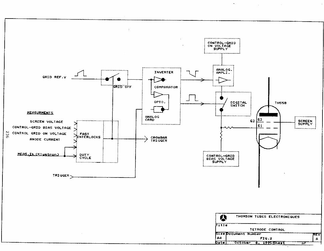
. .,..—
AGRID REF.V d L
u
. . . . . . . . .
—-
....... .......................,; CONTROL< RID ~: ON VOLTQGE :
SUPPLY ~............... ..............,
I.......J. . . . . . . . . ..................................
....................... ~ QN9LOG. ~
/:: RHPLI. :
● ;~ “sTER ! ‘~ iu~
COMP9RRTOR :; . . . . ..l . . . . . . . . .
b
SCREEN VO~TRcE .---. - . . . . . . . . . . . . . . . . . . . . . . .
5CONTROL~RID BIGS VOLTQGE y;
CONTROL GRID ON VOLTQGE ; F9ST*NTERLOCKS _
ANODE CURRENT>
....
.................—. ........... ..!
‘RIGGER~
OPTO. I
i QNQLOGj CQRD. . . . . . . . . . . . . . . . . . . . . . . . . . . . . . . . .
CROUBRRTRIGGER
t... ........................,
b~~f;~fiL ; TH558
. . . . . . . . . . . . . . . . . . . . . . . . . . . .
I ~
‘ ‘+ ~
Im . . . . . . . . . . . . . . . . . .~~ 62 _ : SCREEN :
61: SUPPLY ~
—— . . . . . . . . . . . . . . . . . .
—1
...............1. . . . . . . . . . . . . . .
j CONTROL<RID :, BI QSSUPVPOLLJAGE :
. . . . . . . . . . . . . . . . . . . . . . . . . . . . . . .
I L* THOMSON TUBES ELECTRONIQUES
Title
TETRODE CONTROL
%Axe P ocuwnt Nu6er
FIG.2 I aOtt ober 6, 1H5 ~ beet of

TUBES
2.3.3. Hard-tube specifications (TH 558)
~eratin~ conditions
T
Anode voltage continuous 35 kV
Control-grid bias voltage -1.2 kV
Control-grid on voltage +350 v
IScreen voltage 2kV
IPeak anode current 525 A
ELECTRONIQUES
Anode dissipation 55 kW
Filament voltage 23 V
IFilament current 500A
237

I
,!
t
~~ WOMSON TUBES ELECTRONIQUES
3. PULSE SHAPE CO RRECTION
3.1. Pulses hape distortion due to
- Tankcapacitor voltage droop (2 70)
- Pulse transformer transient response (rise time :12 psec)
Versatility of hard-tube modulator
Changing pulse amplitude
Pulse length
Droop compensation
pulse shaping
Feedforward feedback loop
238
atlow voltage level

3.2.FEEDFORWARD FEEDBACK LOOP
This method is based on the errors evaluation between the klystronpulse and the theorical reference pulse.The theorical reference pulse takes into account the theorical limitsof the system (finite rise time).A specific shape is elaborated with the following parameters :- pulsewidth (CD)- reference voltage (CV, CN)- rise time (CT)-. angle of phase difference (leading)- correction parameters
synchronisation mode
The klystron pulse is acquired by an
A computer calculates the voltage
numerical oscilloscope.new reference which will be
applied-to the control grid by a programmable waveform generator.
The hardware (fig.3) and software (fig.4) architectures represent a
complete system to control the modulator operating in remote
modes.
239

:.. . ...... ;......... i........
I
-
-
\............... .:
A
\
240

.... .,
...................................................
MODULATOR
KLYSTRONREFERENCEPULSETfiBLEVkref Ct)
‘-”-”-”T---”””””--”------. *
GRID KLYSTRON ERRORINITIQLPULSE
MEASUREMENT CALCULATIONPULSE
T QBLETGBLE
T QBLE e<t )=Vkref-VkmeasVQiCt> VkmeasCt>
●
I
CORRECTION CorCt>CQLCUL9TIONTABLEfingle of phase
~iff~renceC leading_ Correction
parameters_Smoothin~
TH55S
w\
I TI MF LOOP 20ms-
~ THOMSON TUBES ELECTRONIQUES
/
REFERENCE PULSE TGBLE ELABORATION
F16.4 REF
October 6, 1995 ~ beet of

— f~ ~oMsoN TUBES ELECTRONIQUES
3.3. c ONCLUSION
Results of experiments are presented on figure 5 for a nominalpower operation at 25 Hz.
. + 0.06‘/0 on the plateau
. + 0.3 ‘/0 on the total pulse
These values are in good agreement with the hard-tube modulatorspecifications. The target value of+ 0.1 ‘/0 is obtained on the plateau.Two main perturbations remain :
- The voltage droop at the end of the pulse- The rise time oscillations
The first perturbation is due to the transformer and tetrodesaturation.The first point could be improved by a premagnetizing circuit andthe second one by raising the control-grid on voltage supplyprovided that the tetrode cross voltage stays superior to the tetrodesaturation voltage.
The second perturbation is due to the digital switch which storesenergy into the transformer parasitic elements (leakage inductanceand capacitors). Some solutions exist and have to be analysed toprove their faisability :
- To raise the cathode pulse rise time by :- Raising the rise time of the digital switch- Using an analogic amplifier with a larger dynamics
(-1200V to 350V) instead of Oto 350V
242

.-.
—
1iO
1.
‘, wnm A- m .C3
< E.,. : Cn-::. . .
:..
----1 +.. L———--—,..
. .. .
. . .,.,.1 :.: . .
.. . ..:.. .. .
.. . . . . . . . . .. .. .. .. .. .. . .. .
. .
. ... . . . . . . . . . . . . . . . .
,... . .. . .,... . . .. .. . . . . . .. . . . . . . . . . . . . .. . .. . .. .. . .. .. . .. . .. .
Q..-
.
. .. . . . . . .- .. :..-. . . .
. . .:.. .
::.. ..:. . . . . . . . . ... . .. .
,..
. .. .. . .. . .. . .. . ..
. .
,.
—
. ..,. . . .. . . . . . . . . . . . . . . . . . . . . ... . .. . ... ... . .. .. . .. . . . . i
. .
,,.-
>>L

I
Upgrading the CTF modulators to a peak output power of 45MWfor the Compact Linear Collider Test Facility CTF-2
P. Pearce
1. Introduction
The present CTF modulators are copies of those used in the LIL pre-injector for LEP and are designedto operate with 35~ S-band klysuons at 100Hz and with an RF pulse width of 4.5ps. The newCTF-2 test facility requires 45N @ RF power pulses at a 10Hz rate. The low power RFsynchronisation scheme must inject drive power into new 45W klystrons every 10th modulatorpower pulse so nol to over-drive the RF gun of the test facility, or the modulators made to work at10~. In order to make a significant demonstration of the CLIC two km acceleration scheme, a newhyout requiring higher RF power is proposed for the new probe Wm. the drive bm swtions and forthe new beam loading compensation cavities. This new test facility layout is shown in Figure 1.
3GHz+E 3 GHz-E&o
Rf gun10OMeVlm
DRIVEBEAM
HCSI
1
xvz3m
n
7~‘ ‘r 3
40 UWatts30 GHz
PROBE n 4BEAM ‘- ~
SAS
m3 GHz
<-12m -lOm
>
SAS: STANDARD ACCELERATING STRUCTURE CTS: 30GHz CUC TRANSfER STRUCTUREHCS: HIGH CHARGE SECTION CAS: 30GHz CLIC ACCELERATINGSTRUCTURE
Figure 1. CTF2 test facility
2. Wystrons for 45MW operation
Two European 45W S-band pulsd klystrons are available from Thomson and Valvo-Philips thepresent suppliers of LIL klysuons. The Thomson 45m klysuon ~2132) is ~r~dy in use wi~ tieSincroKone Trieste laboratory who have 10 modulators with these klystrons operating in Lheir 10Hzrepetition rate linac. The Valve-Philips klystron (YK1645) is a derivative of their 35W tube and isat the present in development. Bothof these tubes are mmhanically and elwtricdly compatible withthe present 35W models such that they are plug replaceable without major mechanical changes. Aswell, the same feed coil assemblies can be used for both the 35 and 45~ klystrons. Wch model oftie new 45W klystrons have two horizontal arms from the output cavity so that a reeombiner isrequired when connecting up these klystrons to the machine. The Thomson reeombincr operates invacuum whilst its RF windows are for use with SF6 gas. Two additional RF windows are then ndedbetwmrt the klystron windows and the reeombiner for the accelerator vacuum to k independent fromthe klystron. The Valve-Philips rwombiner works with SF6 gas so that only one extra 45W RFwindow would be r~uird between the reeombiner output and the accelerator vacuum system. Bothrwombiners will h fitted with arc detectors. These different arrangements are shown in Figure 2.
Paper presented at the 2nd Klystron-MtiulaWr workshop at SI,AC for Futur; l,incar Colliders 9th to I Ith octohcr 1995.
244
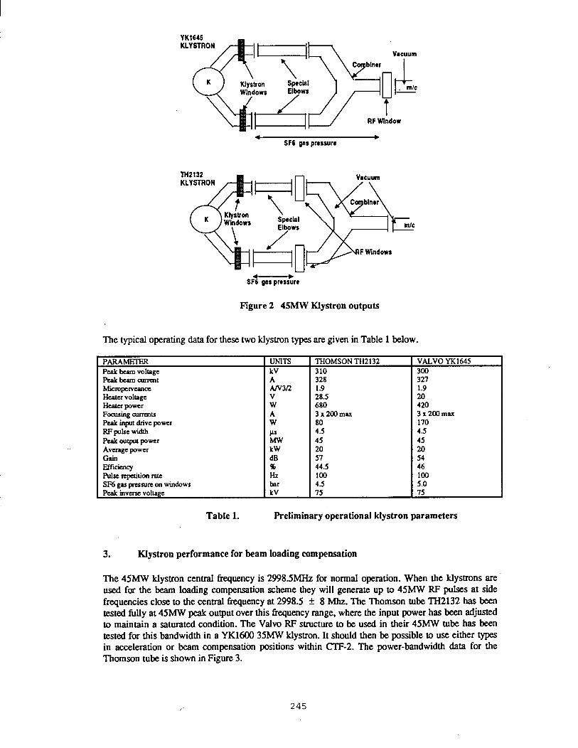
4 bSF6 ws pressure
SF% ws press~re
Rgure 2 4W Wystron outputs
The typical operating data for these two klysnn types are given in Table 1 below.
PARAHR uNrrs THOMSON TH2132 VWVO K1645Pd h Volmge kV 310 300Pd h ~t A 328 327Wmpmam w3n 1.9 1.9H-r voltige v 28.5 20Hm powr w 680 420F-hg ~rs A 3x200mm 3x2~mmP+ -t five power w 80 170RFpoke Mti ps 4.5 4.5P* owtpotpomr m 45 45Avqe power kW 20 mGk dB 57 54Wfitiq % 44.5 46hlw @tiorrw b 100 100SF6g=~u on tidows kr 45 5.0Psskrnvem Voluge kV 75 75
Table 1. Preliminary operational Mystron parameters
3. Wystron performance for beam loading mmpenaation
The 45MW Mys@on central tiquency is 2998.5- for normal operation. When the tiystrons are’used for tie k loading compensation =heme they will generate up to 45MW N puks at sidefrequencies close to the centi @uency at 2998.5 + 8 Mb. The Thomson tube ~2132 has -tested fu~y at 45MW @ output over this frquacy range, where the input power has been adjustedto maintain a saturated wndition. The Volvo N structure to be used in heir 45MW tube has &ntestti for this bandwidti in a YKIW 35MW Uystron. It should then be possible to use either typesin acceleration or km compensation positions within ~-2. The power-bandwidth data for theThomson tube is shown in Figure 3.
245

loo+ ----! \---!---- l---- .4k..:.--k----l - .-. --1----1
4. Wystron Rf output phase stability versus high vo!tage stibility
The output phase stabitity is dependent on fie stabitity of the high voltage puke applied to theMystron. The phase shift over the active Mys@onlength, between input and output caviti=, can bewritten as in (1) where 6 is in radians and d is the length be~mrt the Mystron input and outputmvities in metres.
=[’-(+k)l-+mdians ‘1)
~ = 2xfd
The elwrncrd phase shift per Hovolt of change has been dculati below for a Mystron operating attwo voltages corrmponding to 40 and 45~ output power using data from a TH2132 Mystron. TheValvo Mystron should have a very simik performance.
AO/AVks 1.8 de-s per kV vtiation
The pulse to pulse voltage accuracy of the D’qing system is about* O.1% giving about 0.56 degrmvariation at 310kV. The periodic voltage ripple creatti by the PFN’s 25 Ium@ im~nce WUSdsocontribute to the ovedl b energy fluctuations and phase smbility. The typid m-ured voltageripple from a PFN is about* 0.25% or 1.4 degrees of phase jitter. If both ptdse to puke stabifity andPFN voltage ripple add, the total phase variation is about 2 degrees with the Pm contributing a largerproportion. Therefore good PFN adjustment is important to reduce this ripple to a minimum.
5. Puke transformer and load matching
The present 35W Mystrons o~te with a maximum puke voltage of 270kV, and a Pm volmge ofabout 4 lkV for a new ktystron of this ~. There is a positive 10% mismatch between the Mystronload and Pm irn-ces. To obtain a 310kV puke eitier a higher ratio transformer cm be used orthe primary PFN voltage can be increased. From these two options a larger turns ratio pdsetransformerhas been chosen for We 45W design upgrade. The choice of the turns ratio is linked tothe referr~ Mystron impedance, the Pm impedance, the amount of mismatch desired as well as themaximum primary PFN voltage. To optirnim tiis, a voltage mismatch expression (2) derived fromthree parameters and using the simple wuivelmt circuit of Figure 4, is obtained.
246

VP.]‘ ‘p’”‘–@v*kl;-Hgure 4. Equivebnt output circuit
The mismatch is ~ = ~ Figure 5) at the tiystron, and the mismatch equation using a step-upV k~
transformer of ratio N and efficiency q is: Vtiy=Vpfi.N.q(2-m)
(3)
-1+ .00K I I I I I I I I 1u 1.40U 4.eo, 7. 20u 9.60” 12,
figure 5. Percentage voltage mismatch
The ratio @ is plotted against mismatch in Figure 6 for tiee transformer turns ratios. This showsVpfn
that to maintain the centre of the design at 10% impedance mismatch and generate a voltage pulse of310kV for 45W operation a transformer ratio of 1:14.8 is n~ed with the PFN charged to 40.4kV.The present 1:13 ratio pulse transformer would require a PFN voltage of 47kV for the same conditionsand is close to the peak rating of the present PFN apacitor reducing ovedl reliability.
8 ---- --- - - 71&l: f48--- --------I ma~ %
1 * ~[ 1-------j~--i------~-
I 1—
Figure 6. Impedance mismat~
2:7

6. The Thyratron ~tch
The thyra&onswitch used in the 35W modtdators is the ~V CX1836A. This tube has a muimumpeak current capability of 10kA and will operate up to 50kV anode voltage. The conditions in tieupgraded design will require a maximum 5kA anode currentwitiapproximately4lkV maximum
anode voltage. The peak thyratrort current as a function of positive mismatch is given below
I&y =Vpfn Amps
R Hy(2 - m)(3)
At the 45W operating conditions where the Uystron perv~ce p = 1.9. 104 M15, the Pmvoltage 40.4kV, N= 1:14.8 and with m = 10% gives a peak thyratron current of 4926A. me averagecurrent is 3.2A so that the MS current is about 125A. The thyratron parameters for the upgradedmodtdator design are shown in Table 2 below.
$
Parameter Uni@ CX183dA thyratron ~ uwradeAnodevoltage(rnax) kV 50 41Anode mmt (mx) M 10 5.2Averagec~t A 10 3.2Anode heating famr VW 300.109 21.109
Table 2. Thyratron requirements
7. The Pulse Forming NeWork (PFN)
.The present Pm has 25 CCHS=ch having an inductance L = 0.625@ and ~pacitance C = 25nf withan adjusted impedance of about 5 ohms and 10~o mismatch. To maintain a puke fit-top width of atI=st 4.5w in the upgraded design, the puke width at 70% must be about 6.3w. With the hgertransformer step-up ratio the new Pm impedance must be a lower value to match the new referredUystron resistance of about 4.32 ohms. The adjusted value of the new Pm impedance, with 10%mismatch, will be about 3.9 ohms. This amount of change is not possible witi the tuning inductorsalone, and the Pm capacitor value has been increased to bring it into this mge. Taking into acmuntthe apacitor tolerances of fi.5% and the maximum tuning range on the wll inductor, a 32nf vrduefor the cell capacitance was chosen.
8. End-of-line and inverse voltage protection
The end-f-line diode -resistor network in parallel to tie Pm absorbs negative voltage reflections onthe line and at the thyramon anode. These reflections can come from intermittent short circuits in theklystron or its tank assembly. The front end snubber network fitt~ across tie sending end of thetri=ial pulse cable is used to &mp out the fast reflections that are generated when the rising edge ofthe thyramon pulse hits the pulse mansfomer inductance. These voltage spikes travel up and down thetriaxial cable and could cause problems to it and the thyratron if the snubber network was not present.
Ill———~ m~a
(EO LC A L
TNL CUPPER +
10 ohm
m mtio 1:14.6
Figure 7. Basic modulator circ~
248

A new tail clipper circuitklystron voltage fauns that
protection element has been added, as in Figure 7, because of inversehave occurred in the present modulators. If during the high voltage pulse
the thyratron ceases to conduct the magnetic energy stored in the pulse transformer creates a largepositive voltage pulse at the klystron calhode. Figure 8 shows the normal klystron voltage pulse andan inverse klystron voltage fault that has occurred without a tail clipper.. This inverse voltage cancause internal breakdowns in the klystron gun structure. The tail clipper network will prevent thishappening and does not have an adverse effect on the positive mismatch, but must be designed so notto affect thyratron recovery conditions.
figure 8. Normal and inverse fault voltage klystron pulses
9. Summaryl
All components described have been designd and integrated into the present modulator sncture.The modulator performance with tiese new components has krt simulated under normal and faultoperating conditions successfully. An SCR command charging system is being developed for theresonant (charging time t=4ms) high voltage supply. This will enable the modulator to operate at ratesbetween 10 and 100Hz without having to maintain high voltage on the thyratron anode for longperiods, and avoid PFN voltage droop at the low 10Hz repetition rate. The projmt schdule requiresthat the first of the three modulators be upgraded for an wly 1996 operation of the CTF-2 testfacility.
10. References.
i. CLIC Drive Beam Study Team, “Two days for a Two-Beam Accelerator in theCTF-2”, Femey-Voltake, France, 15th and 16th December 1994.
ii. P. Pace, “A design proposal for upgrading the CTF modulators to 45W”, ~RNCLIC Note No. 268, March 1995.
...111. M. Akemoto and S. Takeda, “Pulse Modulator for 85W klystron in ATF linac”
17th International Linac Conference 94, Tsukuba, Japan, August 1994.
iv. R. Cassel, “Command Charging for the SLAC klystron-modulators”, CERN-PSKlystron-Modulator workshop, Note PSAP 92-06, Geneva, October 1992.

.
Power Modulators Based onAdvanced Transformer Line Methods *
1.Yampolsky and M. ChoiIntegrated Applied Physics
M. GundersenU.s.c.
An approach to modulator design is described that has the followingadvantages:
. Overcome rise time limitations imposed by switches andtransformers, for high voltage, high power transfer operation
. Reduce dependence on high voltage switch-transformercombination
. Produce a design so that each stage has no reflected energy
. Optimize efficiency of energy transfer
Support for this work has been provided by the Department of Energy, the Office of NavalResearch, and IAP lR&D funding.
Integrated Applied Ph.wits Im.Y+@ ~hq & 27rn Baa Ml Amo,Ww #7w Torra~ CA,9~
mtiti m ~1 3@5051W fax M@n351m

General Concept (1)—Smith Approach
*
Vp~ Vch
S - SwitchLn – Pulse Forming Line
● e*eee
Ln
Line Relative impedence Relative charging Relative pulseNumber of the line volwge of the line voltage in line
Ln R(Ln)R(Ll) Vch(Ln)W(S) Vp(Ln)N(S)r
1 1 1 -0.52 3 1 -1.03 6 1 -1.54 10 1 -2.05 15 1 -2.5\ —.-
6 21 1 -3.07 28 1 -3.58 36 1 -4.09 45 1 -4.510 55 1 -5.0
1111 66 I 1 I -5.51121 78 I 1 I -6.0
The chargingpulse voltage
voltage andare given
relative to the switch voltage.
INTEGWTED APPLIED PHYSICS INC.

.—
z
General Concept (2)— New Approach
S1 S2 S3 S4
‘3t-M= **O’*
●
Vchl vch2 vch3
s~vP vch2
V.1 ~1A
Z1 Z2
vch2 - Vpl (1 - 22/21)V.1=
1 + z2/z~AA
S - Switch
L - Pulse forming line
Vch - Switch charging voltige
‘P - forward wave
Vr - reflected wave
I VC,(L.,N(S) ~vpLn;N;s,~o:E,
Line Relative impedence Relative charging Relative pulseNumber of tie line volhge of tie lme volhge in lme volhge
Ln R(Ln)R~l)11 1 I 1 -0.5
1 I I
2 5 2 -1.5 I 33 15 3 -3.0 6
4 35 4 -5.0 105 70 5 -7.5 156 126 6 -10.5 217 210 7 -14.0 28a 330 a -Ia.o 369 495 9 -22.5 45
10 715 10 -27.5 5511 1001 11 -33.0 6612 1305 12 -39.0 7a
The charging and pulse voltage aregiven relative to the switch voltage.The over voltage is given relative tothe switch closing voltage.
INTEGWTED APPLIED PHYSICS INC.

Application Example (2)– 2 MV, 2 kA, 100 nsec Accelerator
1. Water100 kV
e
u
x
Q
\LI
T
L4
TD*d
L5 L6 L
+f Inttiace btwen tine and oil
2@ k,Ik
100kV200 kV
~ TransmissionLin~
L1:2Q50kV L25Q100kVL3: 18~. 200kV L4: 60 Q 4W kV
L5:157fi~kV L6: 295 m 600 kV
L7: 478 ~ 600 kV L8: 703 Q, 600 kV
20 kV
lio,~ 1r To3@’akv
Gncel!ing Line: 140 Q 600 kV
INTEGWTED APPLIED PHYSICSINC.

.,,
\
Magnetic Pulse Flattener – SimulationSimulation circuit configuration
~ia~ = 5250, ~, 6750A Charging Vol~ge: 1.26 MV
lbias L2
Simulation results
.1**
(a) High bias mrrent (b) “Just right” bias current (c) Low bias current
e INTEGWTED APPLIED PHYSICS INC.

—
xwGo
\
4
—
—
—
—
—
—
—
> I
255

The Demonstration Model and the Result
outputvolt;ge
Pulse charging
L I 20.-—~ 16nF A Isolating Line
11~’1000 n 2on
BLTsoon Switch #2
72fi ,36fi, .8 3nF1.5n F
N 12niwa BLT
r4n , 4nF .
Switch #1 12nF
3nF
10
..Each line is 60nsecfora 120nsec pulse length
2-80
Output Voltage- 4 x Switched Voltage -1oo
voltage at 22 kV switchand 800 A load current
o 50 100 150’ 200 250Time nsec
—-
Circuit diagram of two-switchhigh voltage pulse modulator
- INTEGWTED APPLIED PHYSICSINC.

.;
o
s
257

.
THYRATRON LIFETIMES, A BRIEF REVIEW
G.D. Wait and M.J. BarnesTRIUMF, 4004 Wesbrook Mall, Vancouver, B.C., Canada V6T 2A3
1 Mandate for Thyratron Section.
For a good overview of the NLC modulator requirements see references [9, 17]. Tony Don-aldson has posed the following points for consideration during the thyratron section of the
Modulator Switch Session. The NLC modulator switches must reliable, fast and long lived.
If we were to build a LC today with 3000 modulators, we would end up replacing thyra-
trons at the rate of one every two to three hours. Even with a MTTF = 30 khrs, we would
loose a thyratron every 10 hours. The Thyratron Switch session will consider the present
specifications for the NLC (SL.4C style) modulator that follows:
Epfn
Vpfn ~ibtr = tf
tpwPRF
PT ratio ‘Klystron cathode voltage
Klystron beam current
= 360 to 461 Joules, modulator will drive 2 parallel klystrons
= 72 to 75 kV
= 3 kA thyratron anode current
= 300 to 400 ns
= 1.2 us
= 120 and then at a later time 180 Hz
= 7:1
= 480 to 505 kV
= 400 to 430 A for 2 parallel klystrons
. Oxide cathode thyratrons at SLACcurrent density = 30 A/ti2
240 modulators for 5 years [SLC Era] at 5000 hours/yearperformance: epy = 46 kV (2 gaps) , ib = 6 kA, tpw = 3.5 us, f = 120 Hzreasonable lifetime MTTF = 8 khrs
re=onable cost: = 8 k$ for hundredspower consumption: typical heater power = 420 W upto 700 Wtypical reservoir power = 90 W
● Dispenser cathode thyratrons for NLC
(current density *150 A/cm2)performance: epy = 72 kV (3 gaps), ib = 3 kA, tpw _= 1.2 us, f = 180 HzLfetime: MTTF >30 khrs
cost: < 8 k$ for thousands
...,’.
258

power consumption: <500 W
2 Experience on Thyratron Lifetimes
,,
-.,
1. CERN PSAverage lifetime in 200 thyratrons in CERN PS >20,000 hours (low Hz) (approx 108 pulses?),which was probably determined by filament hours[l 1]. Tests done at EEV[15] on a CX1 171
for 9 x 10⁶ shots resulted in a requirement to raise the reservoir voltage by 50 mv. After achange of about 1 volt the tube would have to be replaced. This implies a life of 2 x 10⁸
shots for a CX1171.
2. SLAC
Thyratron experience at SLC with 120Hz operation was described at PAC in 1991 in reference[16] show lifetimes averaging● 5200 hrs at 120Hz = 2.2 x 10⁹ pulses
In a 1992 Power Modulator Symposium paper there were fifetimes quoted[8] as● 16,000 hours at 60 Hz = 3.5 x 10⁹ pulses● 12,000 hours at 120 Hz = 5.2 x 10⁹ pulses
Also thyratron lifetimes b~ed on 243 modulators were extracted from a 1994 paper [12]. We~sume 6670 operation of SLAC per year, b~ed on the age of the oldest tube compared to
its operating hrs. There are a few exceptional tubes which have exceeded 100,000 hrs but itis difficult to tell how many shots this corresponds to.
Rate Tube Replacements Life Life
“(PPS) (per month) (hours) (pulses)
10-60 4.5 26,000 3 x 10960 7.5 15,000 3.2 X 10⁹
120 14 8,000 3.4 x 10⁹
180 (21?) (5,300?) (3.4 x 10⁹?)
3. LANLh a 1990 paper[4] thyratrons were operated for 1010 shots with and without reverse current.
4. Rutherford Appleton LabsThey have converted to hollow anode CX1725 which have dispenser cathodes and an in-
cre~ed reservoir volume. They operate at 50Hz and should have some useful data on Lfetimes by now.
259

I ..’.
_..._.-..—... ... . ....
.
3 Methods for Improvi~ Thyratron Lifetime
1. Select a thyratron manufacturer [EEV, ITT/Triton, EG&G, or Litton].
2. Saturable reactorsThe heating of the anode wi~ be a maximum if the electrons that impinge on the anode havefull energy. If the peak current flow is delayed until the voltage across the tube is collapsed(i.e., low energy electrons) then the energy deposition will be substantially reduced.
Since the relative magnitudes of the erosion for different electrode materials can be closely
predicted by the energy required to melt or vaporize the material{6], it is thus important to
reduce the beam energy.
Measurements were performed at CERN[l O]on an EEV CX1 171 thyratron with saturatingferrites mounted on the anode in a 15 0 system. The measurements showed that, with
ferrites, the commutation losses are reduced by a factor of 7. PSpice calculations done atTRIUMF[l, 2, 3] shown in Fig 1, show remonable agreement with the CERN results. Thecalculated commutation losses are reduced by a factor of 5.3 with the CERN configuration.
Fig 2 shows the calculated effect on the pre-pulse cathode current with and without a satu-
rated ferrite mounted on the anode or on the cathode. When the 72 cm2 ferrite is connected
there is an extra displacement current peak whose magnitude is dependent on the stray
capacitance of the anode and the ferrite (to ground).
Fig 3 shows the mechanical arrangement of the saturating ferrite which was installed in themodified coaxial thyratron housing. Fig 4 is a photograph of the ferrite assembly before
installation in the modified thyratron housing. Fig 5 and Fig 6 show the measured pulseswithout and with a 72 cm2 ferrite respectively. The memured anode displacement current
peak is too large since we had overlooked the stray capacitance of the ferrite when designingthe housing. The high anode displacement current will significantly increase the anode powerdissipation and thus reduce the effectiveness of the ferrite.
Fig 7 shows the calculated instantaneous power in the 300 system with two different CMD5005ferrite areas. The calculations showed that 80% of the total switching loss occurs in the an-ode with no ferrite and that about 4070 of the total switching loss occurs in the anode with
72 cm2 of ferrite installed on the anode of a CX1 171. Note that the power dissipation onthe first and second grids are not effected by the presence of ferrite.
Fig 8 shows the memured voltage rise time M a function of reservoir voltage with and withouta saturable ferrite. The rise is independent of reservoir voltage within the normal operatingrange with the ferrite installed.
We noticed two problems with our design. One is that if the ratio of the ferrite outer diameterto inner diameter is large then the inner portion will saturate before the outer portion, thusslowing the react or swit thing times. The other problem that we had W= that the capacit ante
‘,
260

,:. -. . .. .. .. .... . . ... ..- .
to the ground in the coaxial housing was too high and thus we obtained some smaller O.Dferrite for the next series of tests.
Thepulser wasmodified toaccepta CX2171 (anupgraded CXl171 with a dispenser cathodeand a high volume deuterium g= reservoir) which was borrowed from EEV and life testswere to be done but all further tests were terminated last year along with KAON. HoweverTRIUMF now plans to do a limited series of tests to extend this work for LHC studies.
Measurements done recently at SLAC[14] with a thyratron and a klystron modulator do not
give such encouraging results. The saturable ferrite mounted on the anode resulted in onlya 1070 reduction in the anode temperature rise.
There were some measurements done at LANL in about 1990 with 1010 pulses [4] without
saturable reactors and there were plans to extend the tests using a saturable reactor but wehave not seen the results.
3. Improve electrode materials and design
Oxide surface coated vs impregnated tungsten cathodes (dispenser coated). Porous tungstenimpregnated cathodes in test devices have led to an order of magnitude increase [5] in thefollowing parameters;
. Switch lifetime● Peak and average switch current● Rate of rise of current
6. Reverse currentHollow anode tubes reduce damage caused by reverse current. The effects of reverse current
on a thyratron anode after 1010firnit reverse current is shown in reference[4]. There are paperswhich address details in circuitry to improve impedance matching by modifying details inthe pulse transformer circuit [7, 13] and thus minimize reverse current.
References
[1]
[2]
[3]
.,
M.J. Barnes and G.D. Wait, “A Mathematical Model of a Three-gap Thyratron Simulat-ing Turn-on”, Proceedings of the 9th bternational Pulse Power Conference, Albuquerque
N.M. (June 1993).
M.J. Barnes and G.D. Wait, “Improving the Performance of Kicker Magnet Systemsn,
Proceedings of XVth International Conference on High Energy Accelerators (HEACC’92),
Hamburg (July 1992).
M.J. Barnes and G.D. Wait, “Effect of Saturating Ferrites for the 300 Prototype KickerMagnet)’, TRI-DN-91-K192.
261

I .- .... —.—...............-..
[4]
[5]
[6]
[7]
[8]
[9]
K. Rust and G. DcDuff, “LifeExtensiono fThyratronsinShort Pulse Circuits with theuse of Saturable Magnetic Sharpeners”, Proceedings of the IEEE 19th Power Modulator
Symposium, San Diego, California, (June 1990) pp. 290-301.
M.J. Kennedy, H.C. Grunwald and T.R. Burkes., “Evaluation of Dispenser Cathodes for
use in Gaseous Environments”, Proceedings of the IEEE 19th Power Modulator Symp&sium, San Diego, California (June 1990) pp. 237-242.
A.L. Donaldson and M. Kristiansen, “Utilization of a Thermal Model to Predict ElectrodeErosion Parameters of Engineering Importance”, Proceedings of the IEEE 19th Power
Modulator Symposium, San Diego, California (June 1990) pp. 265-269.
1. Smilanski, ‘(Reducing Thyratron Losses in CVL Modulator”, Proceedings of the IEEE
19th Power Modulator Symposium, San Diego, California (June 1990) pp. 287-289.
A.R. Donaldson and J.R. Ashton, “SLAC Modulator Operation and Reliability in the
SLC Era”, Proceedings of the IEEE 20th Power Modulator Symposium, Myrtle Beach,
South Carolina (June 1992) pp. 152-153.
K. Harris, J. de Lamare, V. Nesterov, and R. Cassel, ‘(600 kV Modulator Design for..
the SLAC Next Linear Collider Test Accelerator”, Proceedings of the IEEE 20tn Power
Modulator Symposium, Myrtle Beach, South Carolina (June 1992) pp. 139-142.
[10] L. Ducimetiere, D.C. Fiander, “Commutation Losses of a Multigap High Voltage Thyra-tron”, Proceedings of the lEEE 19th Power Modulator Symposium, San Diego, (June
1990) pp. 3162-3164; 19th Power Modulator Symposium, San Diego (June 1990) pp. 248-
253.
[11] D. Fiander, K. Metzmacher and P. Pearce, “Kickers and Septa Complex”, CERN, Pr&ceedings of the KAON PDS Magnet Design Workshop, (October 1988) pp. 71-79.
[12] D.B. Ficklin, Jr., “A History of Thyratron Lifetimes at the Stanford Linear Accelera-tor Center”, Proceedings of the IEEE 21st Power Modulator Symposium, Costa Mesa,
California (June 1994) pp. 264267.
[13] L.J. Kettle, H. Menown, B.P. Newton and P.J. Cracknell, “Reliability Upgrade of theHarwell 136 Mev Linear-Accelerator Modulators”, Proceedings of the IEEE 21st PowerModulator Symposium, Costa Mesa, California (June 1994) pp. 124-127.
[14] A.R. Donaldson, “A Hybrid Anode Reactor for the SLAC Modulator”, Proceedingsof the IEEE 21st Power Modulator Symposium, Costa Mesa, California (June 1994)pp. 136-139.
[15] C. Weatherup, EEV, private communication.
‘,
262

~... .,-- .—.—,-..-————. ...-. —. . . . .
!
[16] A. R. Donaldson, R. L. Cassel, and T. S Mattison “Kicker Thyratron Experience from
SLC” IEEE Proc. of the Particle Accelerator Conference, San Francisco, May 6-9, 1991,
pp 3165-3167.
[17] P. B. Wilson, “Development and Advances in Conventional High Power RF Systems’),
presented at the Particle Accelerator Conference, Dallas Texas, May 1995.
“!
j..,
,;1
1
‘,
263

3.0
2.5
2.0
1.5
1.0
0.5
0.0
■ CERN Measurement
~ Predicted (TRIUMF)
o 20 40 60 80Magnetic CSA (cm2)
Fig. 1: Comparison of PSpice model with CERNMeasurements.
264

I I
/ I
IS. L. S. I. RDJRCENT TO RNOOE: ( 143ns, 154R)
\/ ;S. L. S.I. ROJRCENT TO C9THOOE
NO S. L. S. I.: (101 ns,77R)
( 59ns, 409)o on~= —-—_---- ---
4c ; I@ S. L. S. I. RDJRCENT TO C9THOOE: ( 147ns, 293R)LL
5 S. L. S. I. ROJRCENT TO RNODE: ( 141 ns, 151 R)
$ NO S. L. S. I. : ( 99ns, 76R) i
2 ( 96ns, 489)% (57ns,40R)u
uRo~ ‘--. --
20ns 40ns 60ns 80ns 100ns 120ns 140ns 160ns 180ns
Time
-—
Fig. 2: Calculated effect of ferrite (72 cn12 of ~D 5005) on prepulse peaks.
265

\
-------- --—---—--—-7L-- . ---- —--—--— --—.
/ ,@
>----
—--—
I
--d--J--_-.._.-_-----—--—--—--—--_---
Fig.
266
3: 72 cm2 Cl~ 5005 on CX
Y*.--—,11
.--\,/ii
1

Fig. 4: 72 cm2 Cl~5005Ferrite llechanical Assembly.
267

m. .
o
003w
\u—.<
Cathode Voltage (kV)- N uo 0 0
m

30
20
10
0
ANODE
\GAP DELAYED/ PULSE#2
GAP#l
\\
_,lJl, ,,l
10Ons/Div
rig. 6: CX1171 Cathode Pulse ~rith 72 cm2 CID5005 Ferrite on Anode.

1
. .
. .
. .
g.
wm. .0.m
=- . . . . .. .
. .u
m k./ \
\
im-
. .
. . .
.
. . .
.
.
.
.
.
(...
Fig 7: Instantanmua power dtipation in thyratron, ~lculated from ((V. - V*) x 1*), for magnetic
CSA’sof 0cm2, Slm2~d101m2 mnnecMona~e. [PFNpr*cbarge=80 kV; ’~WITCH’=7m;20= 300; paraaitic wpacitance from grading ring to ground= 12 pF; 20 pF stray capacitance from
wtbode to ground; gap turn+n delay =40 m; no saturating inductor].
270-——

r
,
L
mm
‘ti
0-.
Fig. 8: Cathode Voltage Rise Time as aPresence of Ferrite on Anode.
? 271
Function of Reservoir Voltage and

THYRATRONRELIABILITY
andLIFETIME
MODULATOR-KLYSTRON WORKSHOP @SLACFOR FUTURE LINEAR COLLIDERS
STANFORD UNIVERSITY, CA
OCTOBER 9-11, 1995
MODULATOR SWITCH SESSION
H.C. GRUNWALDSR. ENGINEERING MANAGER
TRITON ELECTRON TECHNOLOGY
EASTON, PA 18044-0100
10/10/95
TritonD.C-”-.,Tnn....n.--.............+

THYRATRON LIFE LIMITING FACTORS
NON-CATASTROPHIC WEAR OUT MODES
● GAS CLEAN-UP● CATHODE DEPLETION
GAS CLEAN-UP MECHANISMS
● LACK OF INTERNAL COMPONENT CLEANLINESS- CHEM CLEANING, H2 FIRING, PROCESSING
c CATHODE COATING EVAPORATION● METAL VAPOR
- INVERSE CONDUCTION (MOLYBDENUM)- LOW EMISSION CATHODE/SPARKING (NICKEL)
CATHODE DEPLETION MECHANISMSc EXCESSIVE TEMPERATURE
- HEATER POWER-i2
RMs (R) LOSSES- MARGINAL TUBE DESIGN FOR THERMAL MANAGEMENT- ION BACK BOMBARDMENT
● INCOMPLETE CATHODE AREA UTILIZATION
- GEOMETRY/ASPECT RATIO- INSUFFICIENT AUXILIARY ELECTRODE PRE-IONIZATION
● EMISSION MECHANISM/CONSTRUCTION- CONVENTIONAL, OXIDE COATED, SURFACE SPRAY CATHODE- CONVENTIONAL DISPENSER TYPE- UNIQUE DISPENSER TYPE
MAJOR ISSUE: CATHODE
~itonEI.ECTRON TECHNOLOGY DIJfISION+

The cathode is the most critical component in all electron tubes.
Super power and extremely rapid rate of rise switching application have here-to-fore beenunachievable for thyratrons due to the constraints imposed by large aspect ratio (tall) ,relatively low emission density cathodes of classical, surface-coated construction.
Microwave tubes (klystron and ~T) and UK thyratrons have used simple geometry, dispensercathodes with considerable success. Hydrogen gas, back ion bombardment has restricted itsLIFETIME/application - until now.
As a direct result of recent ITT & TRITON ETD IR~ project work, two patents were issued in1991 which define geometries. . conducive to operation in a hydrogen gas environment and
N
4 describe a theoretically derived method for the design of prac~ical cathodes.&
The novel construction employs a planar (low profile) geometry with well definedparallel to ion flow with emission current density capability an order of magnitudethan benchmark conventional designs. The low profile geometry reduces device(inductance) with a consequent reduction in electron transit time resulting in rapidrise performance.
groovesgreater
heightcurrent
~itonELECTRON TECHNOLmY DIVISION+

.,.
UNIQUE DISPENSER CATHODE DESIGN
c 7.62 CM (3.0”) DIAMETER
● 0.68 KG (1.5 LB)
c 82% DENSITY POROUS TUNGSTEN
c CIRCULAR 1.27 CM (0.5n) HIGH CONCENTRIC VANES
● 25 MM (0.1”) VANE SPACING (5:1 ASPECT RATIO)
● 285 CM 2 TOTAL EMITTING AREA
,4 BAO: ICAO: 1 ALZ03 IMPREGNANT
● MOLYBDENUM - RHENIUM SUPPORT CYLINDER
● 500 WATT TUNGSTEN, POTATO MASHER HEATER
fiitonELECTRONTECHNOLWYDIVWIOX+

276

,.
Q +
GROOVEDDISPENSER CATHODE
GEOMETRY
TritonELECTRON TECHNOLWY DIVISION+

278

United States Patent [191 [III Patent Number:. j,063,324
Grunwdd [45] Date of Patent: NOY. 5, 1991
[54] DISPENSER CATHODE _ EhfmGSURFA~
[75] . Inventor:
[73] Assignee:
[2]] Appl. No.:
[22] Filed:
PA~LLEL TO ION ~OW
Hen~ C. Grusswdd, Bethlehem, Pa.
~ ~rporation, New York, N.Y.
502,078
hfar. 29, 1990
[51] Int. ~.s .......................... HOIJ l/M; HOIJ 61/09[52] U.S. ~. ............................- 313/~ Dq 31316~~
313/632[58] Field of Search ................ 313/346 DC, 609, 632,
313/631, 630
[56] Referent= Cited
U.S. PATENT DOCUMENTS
2,189,6362/1940 Knowles et a3. ..... ...... 313/346 DC
2,452,075 10/1948 Smith ........................... 3 13/346 DC2,937,303 5/19@ Germeshausen ................3 13/632 X2,937,304 5/19W Goldkrg e[ al. ................... 313/6313,849,690 11/1974 Cosco e[ d. ........................ 313/630
Pr;mav Exum;ner—Palmer C. DeMeoArrorney, Agenr, or F;rm-Arthur L. Plevy
[57] AB~~
A dispenser cathode for a gas filled tube is fabricatedfrom a porous metal material impregnated with an elec-tron emitting material and has on an emitting surface atleast one geometric aperture of a given depth and widthand having steep vertical walls which serve to compen-sate for the deleterious effects of ion back bombard-ment.
20 ~aims, 3 Drating Sheets
f-
2
279
21
fiitonELECTRONTECHNOLOGYDIVISION.+

5,063.3241
DISPENSER CATHODE }WTH ENf~NG~ SURFA~ PARALLEL TO ION FLOW
BACKGROUND OF THE INVENTION 5
This invention relates to dispenser cathodes for use indiffuse gas discharge tubes and more particularly to adispenser cathode which employs an emitting surfaceparallel to ion flow.
Dispenser cathodes have been employed for a num- 10ber of years and generally use a tungsten-base material.The modem dispenser cathode consists of a stronglybonded, continuous metilic phase of a refractory me~or metils such as tungsten. The tungsten cathodes areinterspersed uniformly with an emitting material. The 15porous metal matrix acts as reservoir from which theemitting material can diffuse to the surface to maintainan active layer and consequently provide a low workfunction surface for the thermionic emission of elec-trons. This definition excludes oxide coated cathodes, 20pure metal emitters and thonated tungsten. Certaindispenser cathodes employ a porous tungsten structureand are impregnated with a molten mixture of bariumoxide and other compounds which enhance the emis-sion and lower the work function. The density of the 25tungsten structure can be vtied from 7596 to 8590 oftheoretical by volume.
As indicated,” modem dispenser cathodes are wellknown and for a review and examples of such dispensercathodes reference is made to an article entitled MOD- 30ERN DISPENSER CATHODES by J. L. Cronin,published in I. E.E.E. Proceedings, Volume 128, Part 1,No. 1, February 1981, pages 19-32. This article explainsthe various t~es of dispenser mthodes which are em-ployed in the prior art as well as the various matends 35utilized in such cathodes. Thus as one can ascetin, thedispenser cathode has been in existence for quite sometime and essentially has been employed, in gas dischargetuk such x high power thyratrons and so on. Therehave been many problems associated with dispenser @cathodes as evidenced by examples given in the abovenoted reference. A major problem =ociated with suchcathodes is caused by ion back bombardment of thedispenser cathode which occurs during tube operation.The bombardment of the cathode structure by ions will 45deplete the surfaces of the cathode of emitting material.~is of course results in low emission until a new activelayer migrates up from the bhlk. Thus in normal tubeoperations, ion bombardment of the cathode which is aconsequence of the charge transfer in the discharge wdl 50deplete the cathode of emitting material and hencesubswtially reduce the operating =pability and life ofthe cathode and therefore the tube.
It is an object of the present invention to provide acathode emitting surface which substantially eliminates 55the detrimenttd effects of ion back bombardment.
SUMMARY OF THE IWE~ION
A dispenser =thode for w irr a gm filled electrontube. said cathode having an electron emitting surface @with tid cathode fabri~ted from a porous refractorymetal interspersed with an electron emitting material,with said cathode when in operation subjected to ionback bombardment which - deplete said electronemitting material from tid surface, the improvement 65therewith comprising at lmt one groove l-ted onsaid emitting surface and charactetied in having steepverricd walls separated one from the other by a.given
Ldistance with ~id groove being a specified depth withrespect to said dislance to enable said cathode to emitelectrons from said steep vertical walls operating tocause bombarding ions which impinge upon the same tocause evaporated emitting. material and radiated ther-mal energy to deposit on the opposite wall, and, tocause secondary electron emission.
BRIEF DESCRIPTION OF THE FIGURES
FIG. 1 is a top plan view of a circular vane dispensercathode according to this invention.FIG.2 is a cross sectional view taken through line
2—2 of FIG. 1.FIG. 3 is a pafiial top plan view of a straight vane
dispenser cathode assembly according to this invention.FIG. 4 is a cross sectional view taken through line
W of FIG. 3.FIG. 5 is a perspective plan view of a dispenser cath-
ode assembly employing serpentine surface configura-tions to provide vertical vanes.
FIG. 6 is a perspective plan view of a dispenser cath-ode assembly employing panial straight line corrfigura-tions to form vane assemblies.
FIG. 7 is a partial cross section view of a thyratronemploying a dispenser cathode according to this inven-tion.
DETAILED DESCRIPTION OF THE FIGWS
Refernng to ~G. 1 there is shown a top plan view ofa dispenser cathode according to this invention. As seenthe dispenser cathode basically is circular in the topplan view and essentially is of a disk-like configurationas further shown in the cross sectional view of~IG. 2.The cathode includes a relatively large emitting armand for example the diameter of such a uthode - be3 inches or greater. The cathode is fabricated from a82% density porous tungsten block structure which isimpregnated with a mole ratio of 4BaO: 1~0:1 Alz03.These blocks a be machined to provide a concenticring geometric configuration. Thus as shown h ~G. 1the concentric rings or grooves such as 11, 12 and 13provide a series of upstanding vane structures as shownmore readily in the cross sectional view of ~G. 2. fichvane structure such as 15 and 16 is fabricated at a speci-fied height with a specified spacing based on a aspectratio of approximately 5:1. Thus for example, a typicalvane height employed was approxima~ely 0.5 incheswith a vane spacing of 0.1 inches based on this mpectratio of 5:1. The width of the vane or concentric flangeW= dso about 0.1 inches (0.093 inches). This ratio isimportant to provide a prerequisite for a seconda~electron emission factor greater than unity and conser-vation of thermal energy and coating be[ween the vaneside surfaces. As cm be seen between mch vane there isessentially a void or a well as 17 and 18. These wells aredeep enough to allow anode penetration. In this mannerthe well can not be too deep or there till be no emissionrrom the lower -tion of the cathode wells. The verti-=1 walls which exist between the vines enable en-hanced emission surfaces but operate to prevent the lossof erni=ion material by ion bombardment. As one cansee, the vanes are oriented parallel to the direction ofion flow. Hence the vanes are essentially parallel to the~irection of ion flow as denoted by arrow 20 as shownon FIG. 2.
The cathode of FIG. 1 has a diameter of3 inches. Theheight of tich vane to the circular bottom recess being
280 ~itonELECTRON TECHNOLOGY DIVISION.+
-.

5,063.3245
soon aslong= they have opposed emitting surfaces forsecondary emission, emitting material consewation andthermal efficiency. ~us within known duty cycle, peakcurrent and desired cument rise time one can select thecathode parameters regarding the width of the vanesthe depth of the vanes, as well a the separation of thevanes.
Refernng to FIG. 7 there is shown a typical crosssectional view of a thyratron utilizing a dispenser cath-ode 70 according to this invention. As seen the dis-penser cathode 70 is located within the thyratron. Es-sentially the outer shell of the thyratron comprises aplurality of mew] and ceramic cylinders which formul-ate the entire tube structure. Such thyratrons are fairlywell known. The cathode rests on a support cylinder 71which support cylinder is typically brazed to the dis-penser cathode on the slightly indented bottom surfaceof the dispenser cathode, m for example, shown in FIG.2 by reference numeral 21 and FIG. 4 by referencenumeral 35. As seen the bottom of each of the cathodeshas a slightly recessed flange onto which the cathodesupport cylinder is secured by brazing. Typically thecathde suppofi cylinder is 5090 molybdneum and 5090rhenium, brazed to the cathode using @Yo molyMenumand 4090 ruthenium. kated within the cathode sup-pofi cylinder may be the cathode heater. ~e remainderof the tube consists of a grid section 72 and anode sec-tion 73 with the intemd cavity of the thyratron beingfilled with an appropriate gas .74. The stficture shownin FIG. 7 is typical of existing thyratrons exentidlyconsisting of cylinders which have the configuration mshown. The cathode 70 consist of a massive 10.5 centi-meters (4.0 inch) diameter, 560 cm2 emitting area fabri-cated from 8290 density ~rous tungsten block struc-ture which is impregnated with a mole ratio of 4BaO: 1-GO: lA1203. The tungsten blocks fabricating the ath-ode were machined to provide concentric ring geomet-ric configurations as for example depicted in FIG. 1 and2. me vane height was defined as 1.27 centimeters (0.5inch) with a vane spacing at 25.4 millimeters (O.1 inch)b-d on aspect ratio of 5:1. This =pect ratio beingaprerequisite for secondary electron emission factorgreater than unity between the vane side surfac=. Thecathode is heated by mas of a 750 watt potato mashertungsten heater loated within the cathode heat chokewhich is the support cylinder, as for example, cylinder71. The cathode is typically hinted to 1050* C. As irsdi-cated the cathode material is porous btium impreg-nated tungsten materials which are utilized based ontheir favorable concurrent propefiies of low work func-tion (2.2-2.6 ev) and, high melting point &reater than3680W K.). Physid configuration of the cathode is aplanar low profile vane structure of concentric rings orparallel recmgular sections on a common thermallyisolated b= plate. The cathode - be a br=ed assem-bly or structures machined from single blocks. Thus asone a ascertain from FIG. 7, the emitting surface ofthe cathode which is the surface that facm the node ischaracterized by having a plurality of vanes which are
5
10
15
20
25
30
35
a
45
50
55
-ntirdly formed by means of concentric circular 60groovm or straight lin=r SIOK on the surface of thecathode which faces the anode. All the ~thodes have aclosed bottom as indicated in both FIGS. 2 and 4, andthe vanes emana[e and extend from the closed bottom.
I cltim: 651. A dispenser cathode for u= in a gm filled tube as an
electron emitting surface with said cathode fabri=tedfrom a porous refractory med interspersed with an
6electron emitting material, with said cathode when inoperation subjected to ion back bombardment whichundesirably can deplete said electron emitting materialfrom said surface, the improvement herewith compris-ing:
at least one aperture located on said emitting surfaceand characterized in having steep vertical wallsseparated one from the other by a given disucesuch that said steep vertical WAIS of said at leastone aperture extend to a specified depth not toexceed the thickness of said cathode with respectto said given distance whereby said at lemt oneaperture does not pass through said cathode toenable said cathode to emit electrons when heatedwith said steep vertical walls operating to causebombarding ions which impinge upon said wall tocause emitting material to deposit on the oppositewall.
2. The dispenser cathode according to claim 1,wherein said at least one aperture is a groove.
3. The dispenser cathode according to claim 1wherein there are a plurality of apertures on said emit-ting surface.
4. The dispenser cathode according to claim 1wherein said specified depth. is about five thes tid .given distance.
5. The dispenser cathode according to claim 1,wherein said refractory meti is tungsten with said elec-tron emitting material being barium aluminate.
6. A dispenser cathode for use in a gas filled electrontube, said cathode having an electron emitting surfacewith said cathode fabricated from a prous refractorymetal interspersed with an electron emitting rnateriti,with said cathode when in operation subjected to ionback bombardment which undesirably a deplete saidelectron emitting material from said surface, the im-provement therewith comprising:
at l-t one groove located on said emitting surfaceand characterized in having steep vertical wallsseparated one from the other by a given distancewith said at least one groove being a specifieddepth with respect to said distice to enable saidcathode to emit electrons when heated with saidsteep verrid walls operating to cause bombardingions which impinge upon said wall to cause emit-ting material to deposit on the opposite wall.
7. The dispenser cathode according to claim 6wherein said specified depth is about five times saidgiven dismnce.
8. me dispenser cathode according to claim 6wherein said refractory me~ is tungsten with said elec-tron emitting material being barium aluminate.
9. The dispenser cathode according to claim 6 includ-ing a plurality of grooves located on said emitting sur-face and spaced one from the other by said given dis-tance.
10. The dispenser cathode according to claim 9wherein said plurality of grooves are a plurality of con-centric circular grooves located on said surface andspaced one from the other by said given distance.
11. The distance athode according to claim 9,wherein said grooves are a plurality of linear groovesspaced one from the other by said given distance.
12. The dispenser cathode according to claim 6wherein said at least one groove is a serpentine groove.
13. The dispenser cathode according to claim 6wherein the ratio of said depth of &d at l-t one
281 fiitonELECTRON TECHNOLOGY DIVISION__* .

I5,063,324
7groove to said width of said at least one groove is about
five to one.
14. me dispenser cathode according to claim 6 fur-
ther including means for heating the same to a tempera-S
ture to cause electron emission.
15. me dispenser cathode according to claim 4
wherein said temperature is 105~ C. 1016. me dispenser cathode according to claim 6
wherein said meml is 8290 density porous tungsten im-
pregnated with a moie ratio of 4BaO: l~O:lA1203
employed as said electron emitting material. 1s
817. me dispenser cathode according to claim 16
wherein said at least one groove machined into saidsurface.
18. me dispenser cathode according to claim 6wherein said cathode is a disk-like structure having atop circular emitting surface of a given diameter and athickness substantially less than said diameter.
19. me dispenser cathode according to claim 6 fur-ther including a support member coupled to the side ofsaid cathode for supporting the same in said gas filledelectron tube.
20. me dispenser cathode according to claim 6wherein said gas filled electron tube is a thyratron filledwith hydrogen gas.
● ****
20
2s
30
3s
40
4s
so
55
60
6S
282 ~itonELECTRON TECHNOLOGY DIVISION +
-.

STEP 1)
2)
3)
4)
5)
6)
7)
GROO~D DISPENSER CATHODE DESIGN PROCED~
DETEWINE
TUBE DROPVd =
Javg FROM DUTY CYCLE
100 + .833 (Javg)
AVERAGE P~SMA SHEATH WIDTH
Ls =
[
24 X 10-: (Vd)25.9 x 10’ (Javg)
CONDUCTIVI~s
DEFINEJo
GROOVED
= Lsnm
= .85(Javg)
DEPTH= 2(Javg - J~
S(2.5 X 10J)
CURW y
cm
volts
1/3 cm
CATHODE D~NSIONSID = [Ip/Javg( ~ )D-40Ls]
2
OD = ID + 40Ls
1ficm
cm
cm
cm
~itonELECTRON TECHNOLOGY DIVISION +
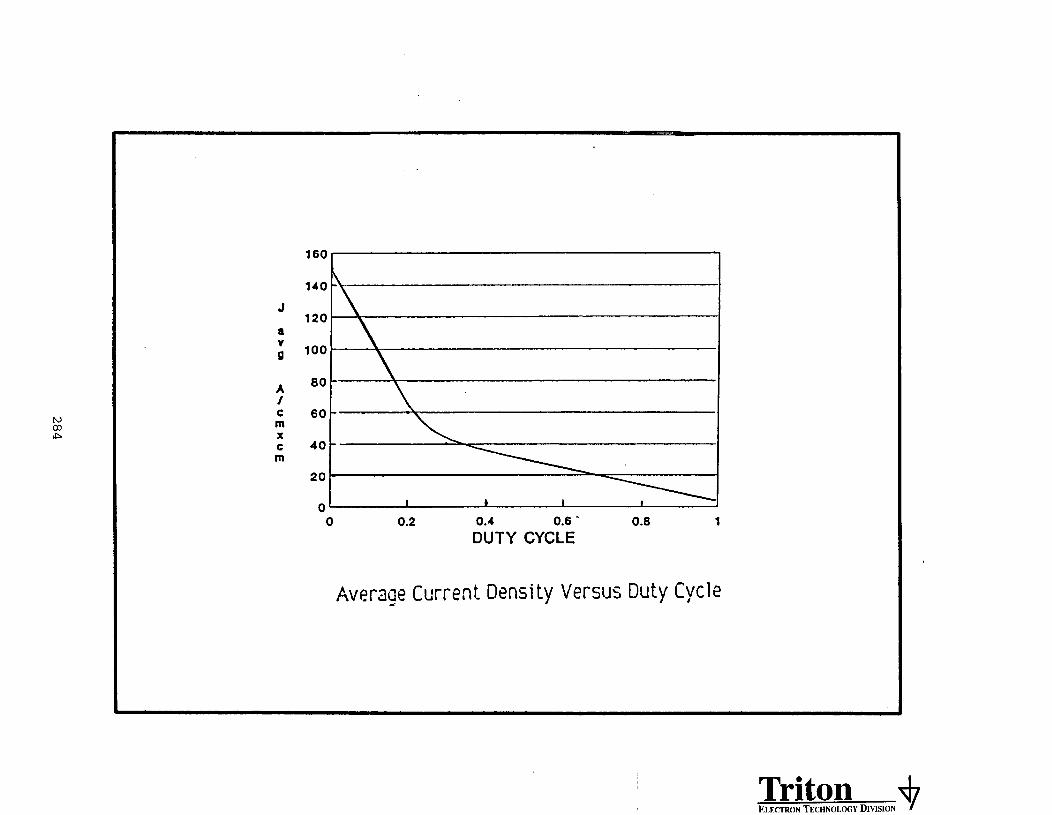
1601 1
140 ~\ IJ
120av~ 100-
\A 80/ t Ic 60 \m t Ixc 40 -m
20
0“ I b 1 i
o 0.2 0.4 0.6. 0.8 1
DUTY CYCLE
Average Current Density Versus Duty Cycle
~itonRLEmRON TECHNOLWY DIVISION +

._ ..._
TEST VEHICLE
PARAMETER
DEMONSTRATED CATHODE PERFORMANCE
ANODE VOLTAGE
PEAK CURRENT
PULSEWIDTH
REPETITION RATE
DUTY (T. S. LIMIT)
AVERAGE CURRENT
ANODE DISSIPATION
AVERAGE POWER
COOLING
LIFE
TEST SITE
(epy)
(id
(tp)
(PPS)
(Id
(P~)
(Po)
F-266
40 KV
4000 a
4 usec base, 1/2 sine
5,000
30 seconds “on”
50.9 ADC, burst
800 x 109 v.a. pps
1.02 MEGAWATTS
OIL IMMERSED
NOT TESTED
PPL, FT. MONMOUTH, NJ
F-241
47 KV
6000 a
5.5 usec ESW
30-120 (VARIED)
CONTINUOUS
4.0 ADC
35 x 10 ‘v. a.pps
96 KILOWATTS
FORCED AIR
40,000 HRS. TO DATE
SLAC, STANFORD, CA

2.141DIA. ~
1.D
I II —
A5.
t I
0.140 HIDEmm w~
[
FE COPPER CORE
1083.C M.P.
k = 3.91~c
~ 5500 , 4.031
r
I /
~RI~O (35Au162m/XCONPRXSSSION BRAZE “L MOL_m FACX
103O”C M.P. 261O*C H.P.kcmwgite - 3.08~c k = 1.42 ~c
. 031J
COWOSITE GRID P~TITION FOR S~ER PO~R ~TRONS
286 fiitonELECTRON TECHNOLOGY DIVISION +

THYRATRON
SUBASSEMBLIES
287 ~itonELECTRON TECHNOLOGY DIVISION+ —.

“CONTIWOUS OP~TION OF A 250 ~ T~~ON” ●
Henry C. Grunwald
ITT Electron Technolo~ DivisionEastOn, PA--
Joseph McGowanElectronics Technology 6 Devices
Pt. Monmouth, NJJohn E. Creedon**
Abstrect
ITT ETD has designed, fabricated and deliveredthree (3) high power thyratrons, Type F259, in whichthe uae of a dispenser cathode is a major desi~improvement. By substituting the diapsnaer cathodein lieu of a conventional oxide coated structure,ITT is attempting to develop a device of extramalyhigh average current capatibility (500 smperea isthe Phaae III objective). Present state of theart ia eight (8) amperea. Two (2) of the F259’shave been tested by ETDL using it’s high powermodulator facilities. Both of these tubes havedemonstrated the feasibility of operating above
the Phase I objective of 18 smpheres. Continuous
operation for” several hours at an average currentof 20 amperea and at a repetition rate of 1000 hartzhaa been achieved. A third tube was delivered toLawrence Livermore Laboratory where it is currentlybeing evaluated in the Pree Electron Laser modulator.
Testing is continuing to establish the ultimatepeak current capability and barium depletion
characteristics on life.
Introduction
Multi-megawatt average power thyratron
performance is a key technology iaaue for successful
Strategic Defense Initiative (SDI) advanced systemsoperation. The initial phaae of a multi-yeardevelopment program has been directed toward theestablishment of an understanding of the physicallimitations and capabilities of aupsr power
thyratrona. Additionally, near-term fabricationof prototype devices was initiated. Work includedthe extension of knom technology to theoreticalmaximums by scaling techni~ea and novel approachedutilizing vast departure frm claaaical design
methods. Development models were manufactured,
electrically conditioned at the ITT ETD Eaatonfacility and delivered to ~L, Pulse PowerLaboratory, Pt. Monmouth, NJ, LANL, Los ti~OS,~ and the Experimental Test Accelerator, LLNL,Livermore, CA for operational and system conformancetesting. The major program milestone achieved,in the first phaae of this taak, was the successfuldesign, construction and teat of a dispenser cathodethyratron with continuous operation capability ofin exceaa of 20 smperea average, at pulse repetitionrates to 1000 hertz.
Objective epecificationa and demonstratedperformance levels for Phaae I of the project areshown in Table 1:
Laboratory
Table 1
Phaae 1 Thyratron Objectives andPerfo=nce Achieved
Parameters
Peak Anode Voltage (epy)
Peak Mode Current (ib)
Pulse Width (tp)
Pulse RepetitionRate (prr)
Average Current (Ib)
0b3ective
25,000
12,500
5
1o-1oo
18
Performance
Demonstrated I50,000 volts
16,000 amperea
5-10 microsec.
100-1000 hertz
21 amperes dc
Technical Approach
Due to the short period of performance allowedfor Phaae I, simultaneous evaluation of keyobjectives, namely cathode, grid and envelope
structure design, wsa performed on common prototype
thyratrons. These prototypes were shipped to thePulse Power Laboratory, Ft. Monmouth, NJ for testand evaluation, after preliminary teat at the ITTETD Easton, PA, facility. ~aluation objectiveswere dictated by the circuit constants of the Ft.Monmouth Pulse Power Test facility and were directedtOWard potential SDIO system applications. Teatswere designed and performed to extract the maximumdata, without destroying the device waler teat.Long-term testing, to further characterize the tubesand to verify life capability, is continuing andis currently in process at ETDL, Ft. Monmouth, NJand LLNL, Livemore, CA. The major milestoneachievement to date is operation at an average currentof 20 amperes for in excess of 36 tillion pdsesat pulse repetition rates of up to one (1) kilohertzfor extended periods (exceeding five (5) hours)without fault, prefire or inverse clipping. Thetubes are still cmpletely operational and furtherevaluation is continuing at increasingly elevatedpower levels. The maximum operating capabilityof the ITT ETD prototype F259 thyratron has not
yet been ●stablished, notwithstanding the PhaseI objectives have been demonstrated.
288 ~itonELECTRON TECHNOLOGY DIVISION.+
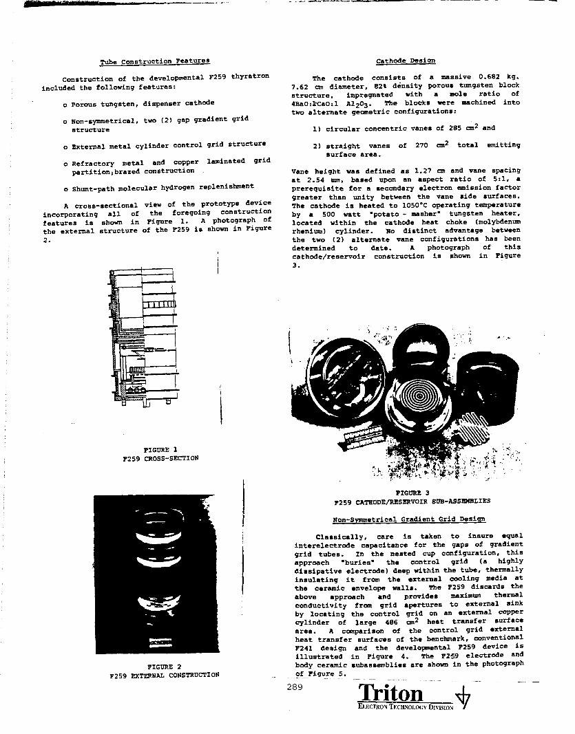
I —.. — . -. . . . .. —.-.--—— -
Tube Construction Features
Construction of the developmental F259 thyratronincluded the following features:
o
0
0
0
0
A
2.
Porous tungsten, dispeneer cathtie
Non-symmetrical, two f2) gap gradient gridstructure
External metal cylinder control grid structure
Refractory metal and copper laminated grid
partition;brazed construction
Shunt-path molecular hydrogen replenisbent
cross-sectional view of the prototype device
incorporating all of the foregoing construction
featurea is shown in Fi9re 1. A photograph of
the external structure of the F259 ia aho- in Figure
I
❑
!
I
F259FIG~E 1
~osS-SECTION
II
I
FIG~E 2
F259 =TERNAL CONSTRUCTION
cath~e De8ign
The cathode consists of a ~asive 0.682 kg.
7.62 m diameter, 828 density porous tungsten block
structure, impregnated with a mole ratio of
4BaO:~CaO:l A1203. me blocks ware machined into
two alternate geometric configurations:
1) circular concentric vanes of 285 cm2 and
2) straight vanes of 270 cm2 total emittingsurface area.
Vane height waa defined aa 1.27 cm and vane spacingat 2.54 mm, baaed upon an aspect ratio of 5:1, aprerequisite for a secondary elactron emission factorgreater than unity between tha vane side surfaces.The cathode ie heatad to 105O*C operating temperatureby a 500 watt ‘potato - usher= tungsten heater,located within the cathoda heat choke (molybden~rhenim ) cylinder. RO distinct advantage betweenthe two (2) alternate vane configuration has beendetemined to date. A photograph of thiS
cathode/reservoir construction is sho~ in Fi9ure
3.
FIG~ 3
F259 ~TEODE@S~VOIR SOB-ASS=LIES
Non-S~ etrical Gradient Gria Deaia
Clasaicelly, care ia taken to insure equalinterelectrode capacitance for the gaps of gradient
grid tubes. In the nested cup configuration, thisapproach ‘buries” the control grid (a highly
dissipative electrode) deep tithin the tube, themallyinsulating it from the external cooling media atthe ceramic envelope walla. me F259 discar~a theabove approach and prwides maximum the-l
conductivity fr~ grid apertures to exte~al sinkby locating the control grid on an etie~a~ ~P*rcylinder of large 4S6 cm2 heat transfer surfacearea. A capariaon of the control grid externalheat transfer surfaces of the benchmark, conventionalF241 designillustratedbody ceramicof Figure 5.
289
and the developmental F259 device iSin Figure 4. me F259 electr~e andsubaasabliea are shown in the photograph
fiitonELECTRON TECHNOLOGY DIVISION+

I
FIGORE 4F259 VS F241 GRID STRUC~E C~PARISON
FIG= 5F259 ELECTRODEMS=LIES
Grid Wterial and AWrture Desire
The-1 conductivity of grid members plays
a major role in super power thyratron OPeretion.Surface thermal integrity, or freedom frm localizedheating and stiae~ent metal vapor arca~ -Y beachieved by the utilization of among others, three(3) construction techni~es:
1) Molybdenum Partitions2) Tungsten Carbide, Flame Spray Costed Copper3) Molybdenum-Cop~r-HolyMenm Laminate
of the three (3), the composite grid Pa~ition ‘hem
in Figure 6 haa proven the most reliable, to date.The high surface melting temperature of rnolybden~(2610°C) iS caplemented by the high themal
conductivity (3.91 watt/~ “c) of the copper core.
hular apertures of 3.5 m tidth -re utilizedin both grid and baffle plates, yielding an effectiveopening area of 21 cm2 in the control grid and 18.0~2 in the gradient grid and control grid baffle.
This e~ates to long pulse, peak current capability
of 29 ka and 25 ka respectively, using the apirically
determined 1.4 ka\cm2 maximum aperture current dansityvalue.
Aperture locations and overlap were calculatedto preclude line of sight anode field penetration.Designs were verified by computer plot of
eWipotential voltage lines tithin the tube structure.The data was obtained frm the solution of the LaPlaceEguation in the ITT ETO Electron Trajectory Progrm(baaed upon the Herrmsnnsfeldt SLAC gun code) fOr
the given geaetry.
A typical ewipotential field plot used involtage field penetration analysis is shown in Figure7.
i
FIGORE 6~OL=D_/COPPER ~INATS GRID
n
290
FIG~E 7E~UIPOTSNTIAL FI~ LIn PLOT
~itonELECTRON TECHNOLOGY DIVISION+

Gas Coolinq BY Molecular Hydroqen circulation
A shunt gas path was included in the construction
by machining 5 m holes in the electrde rings,in parallel to the main discharge path. The shuntgas path benefits were twofold and dramatic:
1) Repleniabent of molecular neutral gas toenhance internal heat transfer.(No.=: Principal cooling of internal tubeCmponents iS accomplished by thermalconduction through the gas.)
2) Provision for a source of electrons to replacethose “pumped” from the gap regions, therebytending to e~ilibrate gas density throughoutthe entire tube.
The aggregate hole was calculated to e-l the anularcross-sectional area of electrode O.D. to ceramiccylinder I.D. space, thus providing a constant pathcross-section for neutral gas flow around the maindischarge path.
Reservoir and Gas Fill
Four (4) large titanium hydride reservoirswere utlized to maintain a 500 micron pressure ofhydrogen gas within the thyratron.Temperature/pressure e~ilibrium was accomplishedwith 40 watts maximum, of reservoir heater power.Particular attention was directed to thermallydecoupling the reservour from the cathode. Potentialparasitic heating of the reservoir at the rewiredsuper power rms cathode currents, due to theassociated cathode ohmic losses, could destabilizethe optimum reservoir basepoint if thermal shieldingwere not arefully considered.
Thyratron Test Data
Electrical conditioning and preliminary test,at the ITT Electron Technology, Easton, PA facility,
waS performed in a 600 ~, 30 ~ DC, line-typemodulator, fitted with a 4.0 ohm, 7.5 microsecond
Pulse Forming Network (PFN), with matched resistiveload. No inverse clipper circuitry waa utilized.Tubes ware operated continuously in air with forcedcooling at Up to peak forward voltages of 54 kvand at average currents up to 7 amparea prior toshi~ent to the Ft. Monmouth Pulse Power TestFacility.
The initial Ft. Monmouth Test Facility consistedof a 3.3 megawatt, 22 kv dc power supply and a 10microsecond PFN having a 3.5 Oh ~pdance. ~
air-cooled Ohmweave load was used that gave a smallpositive mismatch. No inverse clipper circuitrywas utilized. The tube under teat (~T) was immersedin non-circulating transformer oil.
ITT Em type F241 thyratron, shown in Figure4, was selected for initial technology benc~arkdevice capability testing. Reliable operation wasrecorded at:
ePY = 26 kv, ib = 6,500 a, PRF = 184 PPS, Ib = 12 Adc.
Internal thermal devf ce limitations became
evident after fifteen (15) tinutes of operation
at:
ePY = 32 kv, ib = 0,000 a, PRF = 184 pps, Ib = 14.8 Adc.
On the basis of the benchmark evaluation, itwaa concluded that the all copper grid strutiureof the F-241 was capable of 12.5 Adc, continuousoperation, oil tiersed.
The ITT ETD type F259 prototype thyratron shonin the photograph of Figure 2 and in outline in
Figure 1 was then installed and evaluated with the3.5 ohm network. The device was operated for greaterthan 3.6 x 10⁷ pulses (to date) at various repetition
rates (400, 500, 940, 1000 pps) at anode voltagesof 18 to 30 kv for continuous oFratin9 periodsto five (5) hours at 20 to 21 Adc, without fault(high voltage overload), prefire or cliPPin9. Tubeperformance was steady and showed no si~ ofdegrading. Thyratron thermal management designwas verified by the stabilization of anode operatingtemperature at 100°F after 60 minutes of 20 Adcoparation. It should be noted that although the20 Adc average current level and the 1,000 pps pulserepetition rate ~C~~ the project objective goallevels, they represent the maximum current LmL
OF TESTING---not titimste device capability.Continued testing and final characterization ofthe Phase I design will be incorporated into thegoals and objectives of the follow-on phase of thisresearch program.
●A portion of the support for this work was provided
by the Department of Energy, LOS AISMOS NationalLaboratory, ~ and partially funded by E~L andITT ETD.
●*nr. Creedon is a constifint with SRI, International.
Acknowledgements
The authors tish to acknowledge the.significantcontribution to device mechanical design by CharlesL. Shackelford, ITT Em.
291
“
~itonELECTRON TECHNOLOGY DIVISION +__
.—— .—

IModulator Switch Session Summary
D. Ficklin
The presentations and discussions that followed covered these topics:
1. Anode ferrite -no data currently available as to the usefil fifetime extension of
thyratron shots from 108 to 109.
2. Is Lifetime reliability directly related to the number of gaps?
3. Cathode temperature is directly related to the lifetime - Mher discussion on this
subject to include some form of filament auto power reduction.
4. Pre-trigger thyratron instead of dc priming of the thyratron. EEV claims much
improved lifetimes. There is yet no substitiated evidence directly comparing modes of
operation. SLAC has experience, no analysis has yet been done.
5. Positive mismatch - the myth revisited. Much discussion about the utilintion of
positive mismatch versus efficiency.
6. Primary thyratron failure modes - (Turnquist)
Envelope material failure
Envelope depletion
Cathode depletion
Question about anode destruction due to ion bombardment
7. Reverse currents, and fast turn on - a question was raised about the damages
caused by reverse currents in the thyratron. General consensus was that fast reverse
diodes would minimize inverse voltage on the thyratron. Concern was voiced about
speed of diode conduction in limiting the peak value of inverse voltage.
8. Plasma quenching, recovery within the thyratron - use a delay of the network
recharge cycle to allow for a cooling of the thyratron plasma. Note, this ties in with the
usage of smart switching power supplies or command charge circuits.
9. At this point, there was a statement by H. Menown describing his international
experience with various modulator systems and the forms of mismatch that were used.
This was to reinforce the minimizing or elimination of the positive mismatch now used at
SLAC.
Conclusions:
1. Get rid of the positive mismatch.
2. Utilize a reverse diode
3. Usage of dual triggering for lifetime improvements.
4. Use a form of automatic power reduction for the thyratron filament.
5. Full optimization will be required to integrate the thyratron into the modulator to
maximize the thyratron lifetime.
Further Observations and Questions:1. Utilization of magnetics to improve thyratron lifetimes2. Question about choice of 100 kV, 5 kA versus 50 kV, 10 kA thyratrons and related
multi-gap reliability3. Cost of manpower used for thyratron ranging program versus automatic system
and associated equipment. Note here that Fermilab uses 25 kHz for both filament andreservoir power in their floating cathode systems.
4. Question about the anode delay and related jitter and how will that affect thesystem operation. mat will be the specified allowable jitter?
5. Can the thyratrons be produced with current technology for a 50 k hour lifetime?
292

Pseudo-Spark Switch Development
at CERN
for the LHC Beam Dumping System
L. Wcimetiere, P. Faure, U. Jan-n, H. Riege,M. Schlaug, G.H. SchrWer, E.B. Vo~enberg
293

A
❑
IICircumfereeRevolution ~riod =.924Number of co~sion ~ 2 ~ons)
Warn aer~ TeV I 7.0D-~ etic - T 8.65L~i cm-2s-1 ~034
2835Mch spat@ ml~ 7.5125Particlespr b-h 1011
2s1014
294

!m
295

I
●
● Ma~etic field c~●
●
●
- Mse time 3p
- Flat top duration M ~- Fan time lm ~- Peak ma- W 0.8 T
● ~etem:
- Tape wound M cores- Tape thich- Wp- M-et len~h lm- ~ber of mapets 2X12
296
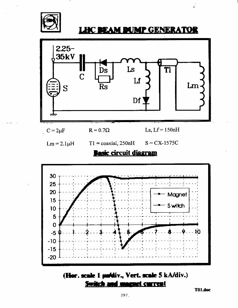
.
C = 2pF R = 0.7Q Ls, Lf= 150fi
Lm=2.l~H T1 = coatial, 250fi s = CX-1575C
30
25
m
15
10
5
0
-5
-lo-15
-20
I-in::””----,----~... ---a ---- ,---- ---- ---- ----
---- ---- ---- --- ---- ---- ---- ---- ---- ---- --
---, - --* ----4 --- L--- A----~------:
+----x --:---- ~---t---- ~----:---l ““-
tx
,
i
--- ---- ---- ---- --- --* :----:---m--:
A S--* ---- * --- 1----4----------- ------ 1---- ”----’
1
h----i----2 ---3----4t--6-4
t---- ,---- ~.-- -, --- -r-
, :1 -A *A
, ,
I-----!----c---------h---J----,---------,----J----‘

I
—
ml~ LHC BEAM DUMP GENERATOR
30
25
20
15
10
5
0
-5
-lo
-15
I
. . . . .
f“.,. . . . .....’- .’. .L .-’
r
“i -I
!“
~??
I-, --,
-201- -’ --’----’
(Her. wa~ 1 @div., Vert. sale 5 k~div.)Switch current——___ _—.
Voltige range
Current amplitude pos./neg.
Current rise/falltime
Current rate of rise/fall
Pulse duration
Charge transfer pos./neg.
Repetition time min. @ 2.25 kV
~p. @ 35 kV
Total lifetime
Prefire rate
2.25-35 kV
+30/ -15 U
3.5/1 ps
15/45 w~s
8 ps
89/20 mC
10 s
6 h
100000 pulses
<<1 o~
Switch requiremew298

l@lSWITCH TYPES
. Thyratrons
● Mdti GTO’s (FHCT’S)
. Pseudo Spark Switches
299

A I ,A
u
CHICANE
INSULATOR
mODE
CATHODE
BIASELECTRODE
FE TRIGGERDISK
GMRESERVOIR
300

,CHIMNE
lNSUMTOR
MODE
~CATHODE
6MELECTRODE
, FE TRIGGER
DISK
u
301

W~WTIC SECTION
~ROUGH ELECTRODES
Anode
\ /
erOsiOfi zOnes
\ cathode /
302
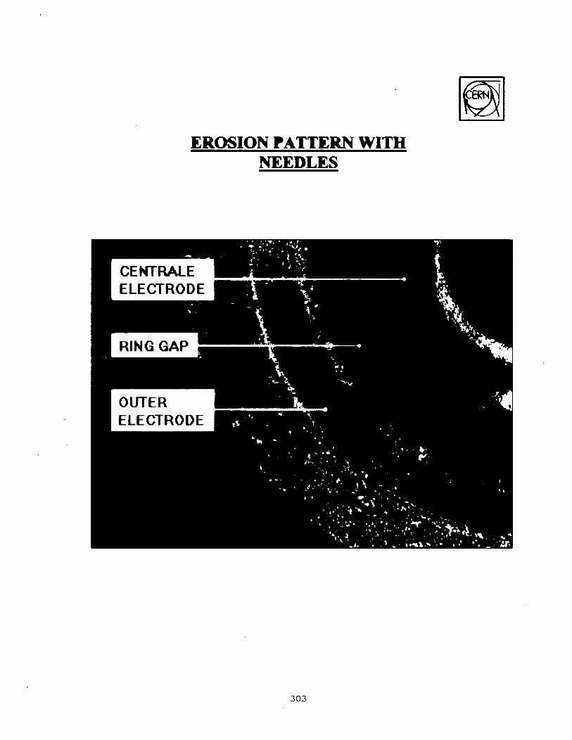
303

. Current quenching and *ps in f-ad v~tagedrop am ~nificant p-ins for our a@htion
● Both d b - to be typical problems of apse~ -rge
We need a better undershnding of these physicalpheno~ h being able to cure them
304

Quenching:
●
●
●
●
●
●
●
●
●
●
●
●
●
●
depends strongly on cleanliness conditions and gas
composition,
depends strongly on gas pressure,
appears only within certain current and voltage ranges,
depends on the transferee charge,
depends clearly on the electrode geometry,
can lead to very periodic “Quenching bursts”,
cannot be influewed by the triggering,
does not appear after the ignition of “hot spots”,
appears favoured in a homogeneous stage of thedischarges,
causes an explosion of the discharge plasma,
is followedby atransitionto a lowerimpedance,
s~s “side-on-seen’*withareductioninthedischargeluminosity,
ends “side-on-seen” with an increase in luminosity andspreading out of the diwharge,
causes often the ignition of “hot spots”.
305

Fomard voltage drop stips:
●
●
●
●
●
●
depend ~mgly on cleanliness conditions and gascom~itia,
start only at a certain current and voltage level,
are shifted with increasing charging voltage / dischargecurrent to earlier time instints,
are from a ce~in voltage range onwards no longerdistinguishable from the main voltage breakdown,
have within a certain parameter range a large timejitter,
are coupled to a transition to a lower impedance,
depend not or only slightly on gas pressure,
depend not or only sligthly on the electrode holegeometry,
cannot be influexed by the triggering,
are not directly connected to quenching,
cause “end-on-seen” a darkening of the outer edge ofthe central electrode,
cause in certain parameter ranges the ignition of “hotSpts”,
are not a consequence of the ignition of “hot spots”,
don’t appear after the ignition of “hot spots”.
306

Appears as a suddend vev f=t in~mpion of themain current in the -m of the diwkge.
c
1 1 I I
2 4 6 8—
T~8 ‘20.9.1995
2.5
2-
1
1
-0.5)
Typical current and anode voltage shapes of a dischargewith quenching
307

I
I into a lower im- of W ** gap. I
6
, 4.8
3,6
? 2,4&
~ 1,2Qk~ou
-1.2
-2.4
---- .,---- .,---- .----- .1 ----
I I />I
-..
—
I ! I 1 1 t 1 I
,.
FOR,VA~ 20.9.199j time[~]
Typical current and ande voltage shapes of a dischargewith a clearly visible forward voltage drop step
308

C~NT & VOLTAGE P~SE S~PES AT A CMGWG
VOLTAGE OF 2 kV & A PRESS~ OF 15 Pa D~G
(a)
100(a) & AFTER -750 DISCWGES (b)
1~ d-s:
2W5W2 120.9.1995
(b) afier 750 discharges:
2 4 6 12 14 1(
[email protected]~e [Wj”
6
4
-2
-21 ; I I I I I I I4 6 8 10 12 14 16
the [~]
. -4
309

10’
10°
10-1
10-4
10-5
10-6
Prefire rate of PSS 10(2(ugetter =5.1 v)
gaps)
/’
/t
15
121.9.1995
max. operationvoltage per gap
,/
/
,/’//
//
/’
0“
■ measur~ potits
I 1 1 1 , 1 1 I , I 1 1 , I
17.5 20 22.5 25 27.5 30 32.5 35
charging voltage per gap [kV]

●
●
Current quenching -n be shiM ~t of b workingrange by ting a suitabie ring gap -try(e.g. -~ *rode diameter: 16 mm) ad dngp~re tting. Another possibility which weintend to investigate could be the addition of a smallpercentage of heavy nobel gases.
Steps in forward voltige drop seem to besignificantly influenable only by the gascomposition.
* We are going to C- out ex~tints with
I ~erent gas cq @ens.
311

1=LQ
>
>00N1
■
ss0
>
0=—
0
sm.
ax00
0
312--,
-

i
Thyratron, Pseudospark Comparison
Hvdroaen thvratron
Anode-grid separation3 mm for high hold-off
0.5 torr
PseudosDark
.
Insulator
Qtho&
*ield
I Mo Anode
dC (heated
II’wbm-l, thermionic)IIH
Cathde
Anode-cathode separation3 mm for high hold-off -
.0.1-0.5 torr
Cathode R-mirI
2
,.

1’
Sequence of Phases
w‘E
Typical current and plasma density as f(t)4 8
—— Ne(O mm)~ 3- ;6
2vm 2 -4’”:70~ 2E1EyL 0 ~ ,:$
?
1000 30000g
t/nsec- 1 \
{
,
I PredischargeI Phase ++
1
Hollow
LCathodePhase
l_.. . . . . . ..__-..-.—-
● Long path breakctow~l , ● Ell]issiotl from hollow . Emission from cathode surface● Electrons from back c:~thodc plasma ● Current 1 to = 100 ~
of cathode ● Current ~ =lkA
Applications● electron beam● ion beam● microwave
Applications● high power switching● electron beam
titi ~uhnen IO15B5BLFsadPs&s~ti
● passive plasma lens
3, :’.
. . . .

The hollow cathode phase plays animportant role leading to super-emission
A uniform plasma is produced during the transient hollowcathode phase
This plasma effectively shorts most of the cathode-anodegap without forming spatially inho~ogeneous arcs, andbrings =anode voltage close (=1 00pm) to the cathode (Avirtual anode is formed close to the cathode).
The voltage applied over a short distance results in ahigh field at the cathode surface (=105-106V/cm)
Because the plasma is uniform, the field is uniformlyapplied to a macroscopic area (=cm2)
The field is amplified mainly by surface defects ratherthan non-homogeneous plasma characteristics (as with atypical arc)

L~...’.’’-’..’’.’....”*l\
\\
\\
\\
\\
\\
\\
\\
\\
\\
\\
\\
\\
\\
\\
\\
\\
\\
\\
\\
\\
\C0●-
.
s
—..
-
mEo&
.
●316
,.

Remarkably fast transition from hollowcathode emission to super-emission,
Transition from “non-explosion’” to “explosive
lo8E:. lllclr. .!ll. frlo ~., ‘~’”. :.
‘processes” occurs nearly 107 :!;.................................................... Delay time of explosion
instantaneously, when neof cathodic micro-
106 ~ ~ ,:................................................... protrusions as a
satisfies the following function of plasma
criterion: 105~.................~...................~..............density (tungsten, 10;4 : w].
[
2C0E:)2~ 104 ~..................................................`..`~"."~"""~7g o
~ ne>fi~=—— *- 103 r::::; ;.................~...................t....................................................................................................q
eUcfl) ~02 : .....................................~.9.....9............................~................../...................~.................1
~o~
for Tungsten, this is: 101~~::.........................................................!...............................................................................01..
i:io!i.................. .......... ~ ~ ; \ \. ....... ......................................../....................~.............o........o ...........7
E&zl~108V/cm
“’~’’’ ~’’’ i’’’ i’’’ i’”i” ‘ ‘
n: = 5 ~1013cm-3 o 0.2 0.4 0.6 0.8 1 1.2 1.4~ (,~19 ~-3)
The Delay changes from SECONDS TONANOSECONDS when plasma density
changes bys 2
--e
\–_ -–– ,

Pseudospark High Power Switches.
● Presently a ‘niche’ between thyratrons and spark gaps
!● “Conveniently” higher current than thyratrons, but shorter life
● Longer life than spark gaps, voltage more variable, but lower ultimatecurrent limit
● Aachen approach improves peak currentwP
m ● Life limiting issues related to electrode erosion
● Triggering stability over life is an issue● The emission process is fundamentally diff~rent than thyratrons. It is
very pressure dependent, and difficult to control over long life
● There are many different types of thyratrons. It makessense to develop more types of pseudosparks

mmATIw SWITC~S, PSEw-SPnK SWITCH Su~YV. Nesterov
me present state of Pseudo-Spark Switch (PSS) Development for ~Ws Large HadronCollider was presented by G. Vossenberg. Schematic cross sections of two prototypes PSS6and PSS7, the second composed of two PSS6 gaps in series, were shown, and design criteria,materials and construction, test results reviewed. Attention was given to an electrode erosionpattern, nede formations as well w to quenching behavior and forward voltage drop steps. Itwas verified that1) Quenching:
depends strongly on cleanliness conditions and gas composition,depends strongly on gas pressure,appe~ ody within certain current and voltage ranges.depends on the transferred charge,depends clearly on the elwtrode geometry,can la to very periodic “Quenching bursts”,cannot be influencd by triggering,does not appear after ignition of “hot spots”,appears favored in homogeneous suge of the discharges,causes an explosion of the discharge plasma,is fo~owd by a transition to a lower im-ce,starts “side-on-seen” with a reduction in the discharge luminosity,ends “side-on-seen” with an increase in luminosity and spreading out of discharge,causes often the ignition of “hot spts”.
l)Forward Voltage Drop Steps:depend strongly on cletiiness conditions and gas composition,start ody at a certain current and voltage level,are shifted witi increasing voltage/discharge current to earfier time instits,are from a certain voltage range onwards no longer distinguishable from the main voltagebreakdown,have within a certain parameter range a large time jitter,are coupld to a transition to a lower impedance,depend not or ody slighdy on gas pressure,cannot be influenced by triggering,are not direcdy connwted to quenching,cause “end-of~seen” a darken~g of the outer edge of the central electrode,cause in c- parameter ranges the ignition of “hot spots”,are not a consequence of the ignition of “hot spots”,don’t appear after the ignition of “hot spots”.
Conclusion:Current quenching and steps in forward voltage drop are signflcant problems for ~~application,Both of them seem to be t~icd problems of pseud~spark discharge,Better understanding of these physical phenomenon is needed.
Gunderson offers a succinct conclusion on page_ which eliminates (at this time) thepseudo-spark as a modulator switch for the requirements of this workshop.~ese remarks are repeated below:
Pseudo-sparks operate at higher current than thyratrons but for shorter fifetimes.Pseudo-spark triggering stabitity over life is an issue.More pseudo-spark development is needed.
319

.
SOLID STATE S~TCH ALTERNATIVES FOR KLYSTRONMODULATORS
M.J. Barnes and G.D. WaitTRIUMF, 4004 Wesbrook MaH, Vancouver, B.C., Canada V6T 2A3
1 Specifications for Switch for Klystron-Modulator
The Next Linear Collider at SLAC will require some 3000 Klystron-Modulators: the following
:1
specifiutions apply for the switch for the Klystron-Modulators [l]:
Blocking voltage = 75 kV
Current =3kA
Flat-top pulse width = 1.2 ps
Pulse rise k fall tima = 300 ns
Repetition frequency = 180 pulses per second
Therefore:average di/dt to current peak = 10 kA/ps;average current 1 A.
●
For the Klystron-modulator application under consideration a closing switch is required.
Reliability is a major issue, and therefore the switch should be conservatively rated (e.g.,
for voltage, current, di/dt, power dissipation). A semiconductor switch would have to be
constructed from one or more stacks of individual semiconductors: hence snubber circuitsand dc grading circuits will be required.
If a thyratron switd is used for the modulator, it is desirable that it has a life of at le~t30,000 hours at 180 pulses per second[l]. This paper briefly reviews the available semicond-uctors (see Figures 1 & 2) so as to identify a possible alternative switch, with a life of
significantly more than 30,000 hours, for the klystron-modulators.
2 Summary
‘MOSFET:
SIT:
BJT:
,,
of Abbreviations
Metal Oxide Semiconductor Field Effect Transistor
Static Induction Transistor
Bipolar Junction Transistor
320

IGBT:
MCT:
GTO:
HDGTO:
PC Switches:
3 MOSFETS
Insulated Gate Base Transistor
MOS-Controlled Thyristor
Gate Turn-Off thyristor
Hard-Drive Gate Turn-Off thyristor
Photo-conductive Switches
& SITS
MOSFETS & SITS are unipolar devices - conduction is mainly due to the flow of one typeof carrier: due to the absence of minority carrier stored charge, these devic~ exhibit f=tswitching speeds (N50 ns), and low gate drive power requirement [2]. On-state resistance
exhibits a positive temperature coefficient, therefore these devices are suitable for paralleling.
3.1 MOSFET
Figure 3 shows a summary of the ratings of MO SFETS available from Advanced Power
Technology (APT). These MOSFET ratings lie in the range from 1000 V, 11 A continuous
(44 A pulsed), to 100 V, 75 A continuous (300 A pulsed).
SAL & TRIUMF have positive experience of connecting MOSFETS in series to produce acontinuous train of pulses [3, 4, 5, 6, 7]. Figure 4 shows two stacks of 14 series MOSFETS:
the two stacks are operated in push-pull to produce a continuous train of 106 pulses persecond, of 10 kV magnitude, with rise and fall times of approximately 40 ns[6, 7].
LLNL have tested a MOSFET matrix, with 8 parallel stacks, in single-shot mode, with pulses
of approximately 500 ns duration, at 5 kV and 3 kA[8]. In burst mode (two 5-pulse bursts
of 200 ns pulses) the MOSFET matrix has been tested at 5.3 kV and 1.1 kA[8]: the di/dt
obtained to current peak w= approximately 12 kA/~s.
With a high voltage MOSFET (1 kV) rated at 44 A pulsed (e.g., APTIOOI) the MOSFETmatrix would require at Zemt80 series APTIOO1 MOSFETS per stack and 70 parallel stacks.Allowing for redundancy, and non-ideal voltage and current sharing, the matrix would prob-ably consist of 100 series APTIOO1S per stack x 80 parallel stacks + 8,000 MOSFETS perklystron-modulator. At US$l O per MOSFET + US$80,000 per klystron-modulator.
NOTE: individual MOSFETS would not be paralleled in the matrix, else if one MOSFET
321

I “..
failed to short-circuit it would short out the whole row of MOSFETS.
Conclusion — it is theoretically possible to build a switch for a K~ystron-Modulator using
MOSFETS. However MOSFETS would probably be unsuitable because of cost and complex-
ity (number of MOSFET’S required), and the physical size of such a switch.
3.2 SIT
“The GaAs SIT exhibits fast switching speeds, characteristic of power MOSFETS, and lowconduction losses characteristic of silicon IGBTs. It is therefore a potential replacement forthese devices in the 150–500 volts, 1–10 ampere regime. . . . .. . Discrete SITS could be series-
coupled to fabricate optically-triggered modules, and to achieve a wide range of volt ageratings, up to 5 kV” [2].
Conclusion — SITS are presently unsuitable because of their voltage and current ratings.
4 BJT
Devices are available in ratings up to 1000 V and 80 A (e.g. ESM 4020 from GEC Plessey).
Rise-time is typically greater than approximately 1 PS for power devices.
DC current gain is typically 5 to 10.
Conclusion — BJTs are unsuitable because of their rise-time.
5 IGBT
IGBTs have lower on-state resistance and higher blocking voltage capability than MOSFETS,
but exhibit slower switching speeds than MOSFETS[2].
Figure 5 shows a summary of the rating of lGBTs from several manufacturers. Many power
IGBTs with significant Collector-Emitter voltage ratings have rise-times in the 800 ns range.Advanced Power Technology have a series of IGBTs with maximum rise-times in the order150 ns (70 ns typical). The highest Collector-Emitter voltage in the APT range is 1 kV: theAPT65GL1OOBN h= a rated collector current of 65 A continuous, 130 A pulsed.
With a high voltage IGBT (1 kV) rated at 130 A pulsed, an IGBT matrix would require at
lemt 80 series IGBTs per stack and 25 parallel stacks. Allowing for redundancy, and non-ideal
voltage and current sharing, the matrix would probably consist of 100 series APT65GL1OOBN
per stack x 30 parallel stacks 43,000 IGBTs per klystron-modulator. At US$40 per IGBT
~ US$120,000 per klystron-modulator.
322

NOTE: Individual IGBTs would not be paralleled in the matrix: else if one lGBT failed
to short-circuit it would short out the whole row of IGBTs.
Conclusion — it is theoretically possible to build a switch for a Klystron-Modulator using
lGBTs. However IGBTs areprobably unsuitable because of cost and complexity (number
of IGBTs required), and the physical size of the switch:
6 MCT
Figure 6 shows a summary of the rating of several fast switching and asymmetric thyristors.
Standard thyristors have a limited di/dt capability (e.g. 200 A/ps immediately following
turn-on). Spreading rate is approximately 0.1 mm/ps, therefore a large gate-cathode pe-
riphery is required to ensure uniform dissipation during turn-on[9]: this is at the expense of
conduction losses.
Thyristors with a 100mm diameter junction are available at blocking voltages up to 6.5 kV[9].
AB-B have developed an 11 kV symmetrical thyristor, which consists of 4 (3 kV) thyristorchips stacked in a common housing[l O]. This thyristor has been tested to currents of 50 kAwith a di/dt of 600 A/ps (50 kA waveform is a quarter sine-wave with a time to peak of-200 ps)[lo].
Conclusion — standard thyristors are not suitable because of their limited di/dt capability.
7 GTO
7.1 Standard GTO
Figure 7 shows a summary of the rating of several standard GTOS.
A standard GTO thyristor is optimised for its turn-off characteristics by heavy metal doping,
diffused anode-shorts and irradiation [n]. A standard GTO has a maximum di/dt capabilityof N600 A/ps during turn-on[ll].
Conclusion — standard GTOS are not suitable because of limited di/dt capability.
7.2 Modified GTO (~ thyristor)
With light doping and unshorted anode the device can be used as a CLOSING switch withexceflent turn-on characteristics[l 1]. West code have worked with CERN SL Division to
323

develop a modified GTO (WG200045E6G), which is a symrnetriml 4.5 kV device (66 mm
diame~er junction). The modified GTO hfi been tested to 70 kA, with a di/dt of 20 kA/ps[off-state blocking voltage=l.6 kV][ll]. The gate-drive was 150 V, 240 A peak (200 A/ps),
100 A minimum [i.e., hard-drive]. The modified GTO has a gate-cathode periphery ofapproximately 7 m. Figure 8 shows a current pulse of over 60 kA whish was switched using
the Westcode WG200045E6G modified GTO: the current peak occurs approximately 10 psafter turn-on.
A 250 kA pulser has been designed at TRIUMF for an experiment at BNL: the pulser designutilized the Westcode WG200045E6G modified GTO[12]. The 250 kA pulser consisted of 5
parallel modules, with up to 6 series GTOS per module.
ABB have developed a High Current Thyristor (HCT) with 6 m of gate-cathode periphery (amodified GTO), ~ompare~ with 30 cm for a conventional thyristor-of the same diameter[l 1,
9]. The thyristor is an asymmetrical device (thin wafer for high current operation), andtherefore it is necessary to protect the thyristor against reverse voltage, e.g. with diodes.The thyristor has been tested up to 100 kA with a di/dt of 15 kA/ps[9]: the gate drive w=80 A peak, with a di/dt >50 A/ps.
A switch composed of HCTS with a 30 kV blocking voltage capability for the switch, a peakcurrent of up to 10 kA (maximum di/dt *8 kA/ps), an operating frequency of up to 200 Hz,
and an integrated trigger and cooling unit would cost approximately US$30,000[13].
ABB believe that the switch specifications could be met using modified GTOS: however theshort rise-time would demand a very substantial gate- drive [14]. In order to achieve a suitablegate drive it may be necessary to consider a new semiconductor device: ABB will shortly beannouncing a 4.5 kV blocking voltage (asymmetrical) hard-drive GTO (HDGTO). A 6 kVversion of the HDGTO is expected to be available in early 1996[14]. The 6 kV HDGTO h=
a budgetary price of US$2,500 in large quantities [14]. The HDGTO includes a gate-driveboard. The HDGTO will have a gate-flange (NOT lead) brought outside; a metallized PCBwill contact the flange. This arrangement will permit gate current to flow into the device gatefrom around the full 360° device periphery [14], thus allowing a very hard-drive for the gate.Twenty-three of 6 kV HDGTOS, applied at 3.8 kV DC, per Klystron-Modulator (including
3 redundant HDGTOS) would cost US$57,500 for HDGTOS per Klystron-Modulator. Inaddition diodes may be necessary to protect the HDGTO from inverse voltage.
Assuming a cost of US$1400 per modified GTO (small quantity price for Westcode WG200045E6GGTOS: ABB have also indicated a price of US$1300 for a 4.5 kV [*Asymmetrical*] HCT),
and 28 GTOS per stack + US$39,200 for GTOS per Klystron-Modulator.
Conclusion — a modified GTO is potentially suitable for use in an alternative switch for a
Klystron-Modulator.
‘,
324

8 PC Switches
Photo conductive switch= have achieved the following duties[15]:
at 100 kV & 5 kA (120 ns wide pulses):at 1 kA (120 ns wide pulses):at 1 kA (1 ns wide pulses):
Conclusion — PC Switches aregreater than ~100ns.
unsuitable because
life of 1-2 pulseslife of 4 pulseslife of several thousand pulses
of their limited life with pulse duration
9 Conclusion re suitable semiconductors
The HCT from ABB (a modified GTO), and modified GTO from Westcode are potentiallysuitable candidates for replacing thyratrons in Klystron-Modulators. These device appearto have adequate di/dt and peak current capability. As a result of the voltage rating of
the Westcode modified GTO and ABB HCT, several tens of devices would be required to
be connected in series to achieve the required blocking voltage. Connecting thyristors in
series is a standard procedure in many industries, for example a thyristor valve for use in a
High Voltage Direct Current (HVDC) link can have over 100 thyristors connected in series:
these HVDC schemes are designed for a life of 25 years [16]. To achieve such high reliability,‘redundant’ thyristors are included in the thyristor stack; any devices that fail are replacedduring an annual maintenance period.
The modified GTOS would probably cost in the range of US$40,000 to US$58,000 perKlystron-Modulator.
10 Reliability
In order to ensure high reliability it is important to match the specific characteristics of the
semiconductor device with its application[l 7]. The highest rate of failure of semiconductors
occurs immediately after manufacture, but the process of aging and debugging gradually
lowers this rate: failure rate diminishes with time[17].
In order to ensure high reliability ‘diodes and thyristors should be operated at 50 to 80% of
their maximum voltage rating, and junction temperatures should not exceed 70 to 80% of
maximum rating” [17].
In order to estimate reliability of a semiconductor switch, = a replacement for a thyratron,
use Table 5-1 of reference [17]. Assume a junction temperature of 100° C, and a stress ratio of
325

I
..
0.5 (stress ratio is based on maximum current and dissipation and rated current and dissipa-
tion): from Table 5-1 of reference [17] the Thyristor Basic Failure Rate = 0.022 Failures/l 06
hours. Other factors, such as environmental factors, effect the faiiure rate. However, forthe purposes of this example, round the above Bmic Failure Rate to 0.1 Failures/106 hours.A failure rate of 0.1 Failures/106 hours is consistent with the 100 FIT (failures in time)suggested by ABB [14]. W’here 1 FIT = 1 failure in 109 operating hours.
To achieve a switching blocking voltage of 75 kV, and ~suming a modified GTO with a
blocking voltage of 4.5 kV: apply the modified GTO at say 67% of its rated blocking voltage~ 3 kVl. Therefore 25 modified GTOS are required per Klystron-Modulator. Allow 107o
redundancy ~ 28 modified GTO switches per Klystron-Modulator.
Using a Basic Failure Rate of 0.1 Failures/106 hours x 28 modified GTOS per Klystron-Modulator ~ 2.8 GTO Failures/106 hours/Klystron-Modulator, i.e., 1 GTO failure/350,000hours/Klystron-Modulator. With 3 redundant modified GTOS per Klystron-Modulator,there can be 3 GTO failures per Klystron-Modulator before the Klystron-Modulator needsto be shutdown ~ 3 GTO failure/1,000,000 hours/Klystron-Modulator. This failure rate is
significantly better than that of a thyratron.
NOTE: the estimated failure rate for the sernimnductor switch neglects other components,such ti diodes (required if it is necessary to protect the swit thing devices from reversevoltage), and gate drive circuitry.
The stack of modified GTOS could be modular so that individual GTO modules can be easilyreplaced. Diagnostics at each module would indicate if a device has failed to short-circuit(the usual mode of failure).
11 Other Issues
The following issues will also require consideration:
● An adequate gate-drive, required to achieve the specified di/dt and repetition rate,
may cause excessive gate-dissipation, and thus flashover between the gate and cathode
region[14].
● Referred impedance of klystron, as seen on the primary side of the transformer[l 8]:
how does the referred impedance influence the design of the semiconductor switch?;
● Duty cycle of the PFN voltage: the duty-cycle may effect the blocking voltage at which
the semiconductors can be applied;
1Failure of devices applied at over 3 kV/device are attributable to avalanche turn-on caused by photons[14]
326
●
●
●
●
●
●
●
dV/dt of the reapplied PFN voltage: an exc~sive dV/dt can cause ungated turn-on
of, and damage to, the semiconductor switch [19];
Good matching of characteristics, e.g. turn-on delay time, of the semiconductors (alsoholding of spares from the original batches);
Snubber circuit time-constants;
Non-coherent ttirn-on of the semiconductor devic=: adequate snubber circuits will berequired to prevent overvoltage on one or more semiconductor devic=[l 1, 19];
Fault conditions: maximum voltage, current, di/dt and dV/dt which the semiconductorswitch may be subject too.
Adequate diagnostics are required so that a failed semiconductor can be readily re-placed.
Overall system efficiency must be high[20]: how does the efficiency of the semiconductorswitch compare with a thyratron?.
References
[1]
[2]
[3]
[4]
[5]
[6]
A.R. Donaldson (SLAC): private communication with G.D. Wait (TRIUMF), October2, 1995.
P. Hadizad, M.A. Gundersen, F. Ren, “High-Voltage Recessed-Gate GaAs Field EffectTransistors”, Conference Record of the 1994 Twenty-First International Power Modu-lator Symposium, Costa Mesa, CA (1994) pp. 78-80.
C. Figley, D. Stensrud, ‘A Stacked FET Switch for use in a 20 kV Klystron Modulator”,Proc. of the Eighth IEEE International Pulsed Power Conference, San Diego (1991), pp.1001-1004.
M.J. Barnes, G.D. Wait, and C.B. Figley, “A Variable Duty Factor Beam Chopper for a300keV Injection Beam line”, proceedings of European Particle Accderator Conference,London (June 1994), pp. 2541-1543.
G.D. Wait, M.J. Barnes, and C.B. Figley, ‘A FET Breed Frequency and Duty Cy-cle Agile 6 KV Pulse Generator”, proceedings of 21st International Power ModulatorSymposium, Costa Mesa, CA (June 1994), pp. 97-100.
M.J. Barnes, G.D. Wait, ‘Design for a FET Based 1 MHz, 10 kV Pulse Generator”, Tobe published in the proc. of the Tenth IEEE International Pulsed Power Conference,Albuquerque (June 1995).
327

.,
[7] G.D. Wait, M.J. Barnes, “Measurements on a FET Based 1 MHz, 10 kV Pulse Gen-
erator”, to be published in the proc. of the Tenth IEEE International Pulsed Power
Conference, Albuquerque (June 1995).
[8] H. Kirbie, S. Hawkins, B. Hickman, B. Lee, M. Newton, C. Ollis, C. Brooksby,
D. Gilbert, D. Longinotti, E. Eubank, ‘(Development of Solid-State Inductions Mod-ulators for High PRF Accelerators”, to be published in the proc. of the Tenth. IEEE
International Pulsed Power Conference, Albuquerque (June 1995).
[9] E. Ramezani, A. Welleman, J. Siefken, “High P=k Current, High di/dt Thyristors
for Closing Switch Applications”, Proc. of the Ninth lEEE international Pulsed Power
Conference, Albuquerque (June 1993) Vol. 2, pp. 680-683.
[10] E. Spahn, G. Buderer, E. Ramezani, “High Voltage Thyristor Switch for Pulsed PowerApplications”, Conference record of the 1994 Twenty-First International Power Modu-lator Symposium, Costa Mesa, CA (1994) pp. 93-96.
[11] J. Bonthond, L. Ducimeti~re, G.H. Schr6der, E.B. Vossenberg, M. Evans, F. Wakeman,R. Youdan, “High Current, High di/dt Switching with Optimised GTO Thyristors”,
Conference record of the 1994 Twenty-First International Power Modulator Symposium,
Costa Mesa, CA (1994) pp. 85-88.
[12] G.D. Wait, M.J. Barnes, ‘A 250kA Pulser for BNL EXP 889”, TRIUMF Design NoteTRI-DN-95-18, June 1995.
[13] M. Jung, W. Mayerhofer, M. Edele, O. Gstir, T. Schweizer, E. Zeyfang, E. Ramezani,“Test of Fast SCRS m Spark Gap Replacement”, to be published in the proc. of theTenth IEEE International Pulsed Power Conference, Albuquerque (June 1995).
[14] J. Marous (ABB): private communications with M.J. Barnes (TRIUMF), October 4th
& 5th 1995.
[15] F.J. Zutavern, G.M. Loubriel, W.D. Helgeson, M.W. O’Malley, R.R. Gallegos,A.G. Baca, T.A. Plut, H.P. Hjalmarson, ‘Fiber-optic control of Current Filaments inHigh Gain Photoconductive Semiconductor Switches”, Conference record of the 1994
Twenty-First International Power Modulator Symposium, Costa Mesa, CA (1994) pp.116-119.
[16] M.L. Woodhouse, J.L. Haddock, B.A. Rowe, J.P. Ballad, “The Control and Protectionof Thyristors in the English Terminal valves, Particularly during Forward Recovery”,IEE Conf. Publ. no. 205, 1981, pp. 158-163.
[17] POWEREX Power Semiconductor Data Book: Volume 5, Publication No. 8B-000DW1067/3-87.
328

[18] P. Pearce, S. Hutchins, “Present Performance of the LEP pre-injector Klystron Modula-
tors and the impact of a proposed upgrade”, Conference Record of the 1990 NineteenthPower Modulator Symposium, San Diego, (1990), pp. 124-129.
[19] M.J. Barnes “The Prediction and Control of Transients in Thyristor Valv=”, PhD
Thesis, The University of ~ton in Birmingham, May 1995.
[20] P.B. Wilson, ‘Development and Advances in Conventional High Power RF Systems”,
to be published in the proceedings of the 1995 Particle Accelerator Conference, Dallas,1995.
329

I . .,. -
,.,
u
1
‘,
330

Powemx, Iw, 200 Hlllls Street, rOUn9WOOd, Pennsylvania 15697-lW (412)92S7272Po-x, Europ, S.A. 428 Avenue G. Dursnd, BPI07, 72002 Le Mans, Frsnm (42) 41.14.14
ELEC~lC CAR
11
i
331

.
.,..
80v=G z: Advanced Power Technology MO SFETS
w
w L
0
0
20
Typical values: (Total gate charge, Rise–time)‘nm\o M (\%lnc, wfis>
I I I I I I I I I Io0.0 0.1 0.2 0.3 0.4 0.5 0.6 0.7 0.8 0.9 1.0
Drain–Source Rating (kV)11.

I .
‘,

,,
.,
E
r~iqure 5: Selection of Insulated Gate Bipolar Transistors
600
500
400
300
200
00
00
(Typical rise-time)x Low Conduction Loss
Fast Switching
I
400I
800I
1200I
1600 2000Collector–Emitter Voltage (V)

.
.,
a~ L: Fast switching & Asymmetric ThyristorsI I I
530000
: 20000
15000
10000
5000
0
0I I I
1000 3000 40002000
Repetitive peak off–state voltage VDRM (V)

I *,...
~~ +: standard Gate ~rn-Off Thyristors
3500
1000
500
c 1000 2000 3000 4000 5000 6ReWtitive ~ak off-state voltage VDRM - ~)
di/dt at lTC~
Single cycle surge current (lOms half sine wave)
336
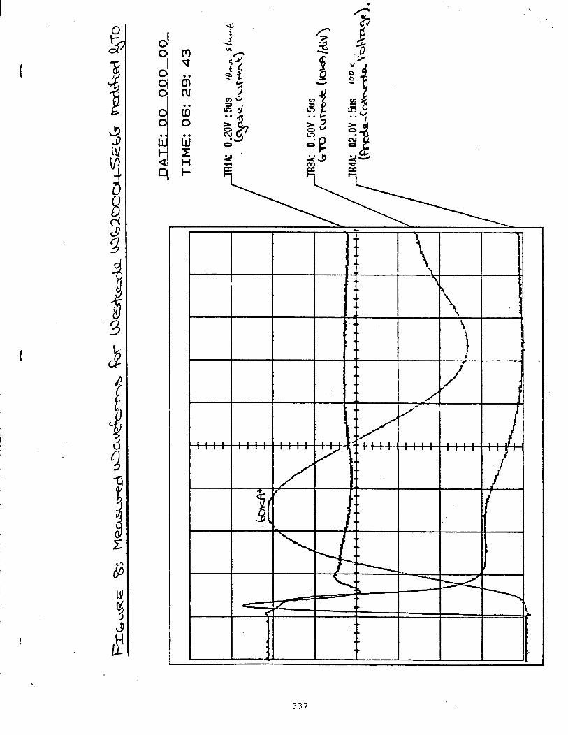
I
(
(
. .
o
337

I 1 1 I1 ! t 1
f
A u + J 1, -.
m*o
o0 o
.0
0
0 0m- o
338

AL~NAnn SWI~~S, SOLID STA~ SWTCH Su~Y
Mike Barnes
Assuming the fo~owing specifications:
75 kV blocking voltage
Wdt = 10 Wps avg.
3 kA current
300 ns rise and f~ times
Modified GTO’S are the most promising semiconductor for the above duty.
Westcode and ABB both have mtiled GTO’S that are closing switches capable of
=20 w~s + =70 Wps.
But tie Westde GTO is the ofly available symmetrical GTO (modified) that I am aware of.
Cost of modified GTO’s for a series stack with 75 kV blocking voltage:
=US$40,000 to US$58,000 for GTO’S,
i.e. 5 + 8 times the cost of comparable thyratron.
Potential reliability of a stack of 28 mtiled GTO’S (assuming GTO’S are conservatively
applid) and with 3 Aundant GTO’S per stack
MTBF => 3 failures/l@ hours~ysmon-modulator
i.e. 25 + 30 times a comparable thyramon (currendy avtiable).
Rquires significant R&D,
e.g. could GTO gate-cathode region be modifidtailord for above duty.
Future improvements to semiconductor switches may make semiconductor switch even more
promistig and rduce cost.
10 stack GTO switch (28.8 kV, 25.9 kA + 127 J/pulse.
● 1 GTO = 13 J/pulse (switching and conduction losses). .
Scale GTO losdpulse ~ 12
● for a ~ystion-modulator switch for NC (if I = 3 kA). .
GTO losdpulse = 13 J x (3,000/25,900)2= 0.2 J/pulse
● loss per GTO at 180 pps => 36 J/see. .
NOTE: above estimate underestimates switching losses and overestimates conduction losses.
~at 3 kA => 12 J/10 GTO’S
=> 12 J/GTO/ptise
at 180 pps => 220 J/s
Thermal resistance of junction to case (double sided cootig)
= 0.017 ‘Cm ~estcode WG200045E~)
● T = 220X 0.017 =N.. .
339

men co- to a thyratrontheGTO switch would not rquire:
heater supply
reservoir supply
gradient grid voltage
Hence adjustment of resemoir voltage is eliminated and ovedl modtiator efficiency is higher.
Other significant factors in favor of the GTO as compd to a the thyratron:
GTO switch does not produce x-rays.
GTO does not ~uire a warm-up period.
GTO does not quire high voltage conditioning.
Easy diagnostics for GTO switch.
GTO has a smooth turn-on: low noise level.
340
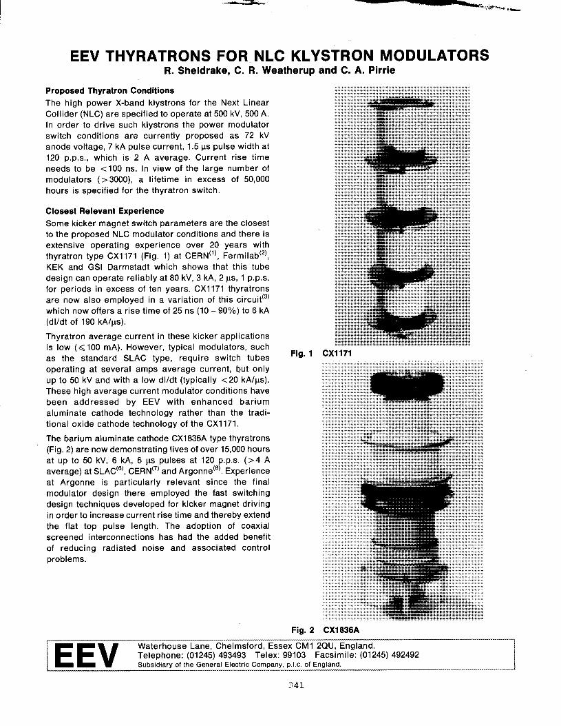
~..,w.+.,_
EEV THYRATRONS FOR NLC KLYSTRON MODULATORSR. Sheldrake, C. R. Weatherupand C.A. Pirrie
Proposed Thyratron Conditions
The high power X-band klystrons for the Next Linear
Collider (NLC) are specified to operate at 500 kV, 500A.
In order to drive such klystrons the power modulator
switch conditions are currently proposed as 72 kV
anode voltage, 7 kA pulse current, 1.5 LS pulse width at120 p.p.s., which is 2 A average. Current rise time
needs to be <100 ns. In view of the large number ofmodulators (>3000), a lifetime in excess of 50,000
hours is specified for the thyratron switch.
Closest Relevant Experience
Some kicker magnet switch parameters are the closestto the proposed NLC modulator conditions and there is
extensive operating experience over 20 years with
thyratron type CX1171 (Fig. 1) at CERN(’), Fermilab(z),KEK and GSI Darmstadt which shows that this tube
design can operate reliably at 80 kV, 3 kA, 2 ps, 1 p.p.s.
for periods in excess of ten years. CX1 171 thyratrons
are now also employed in a variation of this circuit(3)which now offers a rise time of 25 ns (10 – 9070) to 6 kA
(dl/dt of 190 kA/ps).
Thyratron average current in these kicker applications
is low (< 100 mA). However, typical modulators, such
as the standard SLAC type, require switch tubes
operating at several amps average current, but onlyup to 50 kV and with a low dl/dt (typically <20 kA/ps).
These high average current modulator conditions have
been addressed by EEV with enhanced barium
aluminate cathode technology rather than the tradi-tional oxide cathode technology of the CX1171.
The barium aluminate cathode CX1836A type thyratrons
(Fig. 2) are now demonstrating lives of over 15,000 hours
at up to 50 kV, 6 kA, 6 ps pulses at 120 p.p.s. (>4 A
average) at SLAC(6), CERN(7)and Argonne(*). Experienceat Argonne is particularly relevant since the finalmodulator design there employed the fast switchingdesign techniques developed for kicker magnet drivingin order to increase current rise time and thereby extendthe flat top pulse length. The adoption of coaxialscreened interconnections has had the added benefitof reducing radiated noise and associated controlproblems.
Fig. 1 Cxl171
Fig. 2 CX1836A
~
Waterhouse Lane, Chelmsford, Essex CM1 2QU, England.Telephone: (01245) 493493 Telex: 99103 Facsimile: (01245) 492492Subsidiary of the General Electric Company, p.1.c. of England.
341

Proposed Thyratron Switch
The CXI171 will require several enhancements to
ensure reliable performance at the higher average
power of the NLC modulator. Principally this willinvolve the use of enhanced barium aluminate cathode
technology which has already established goodperformance at much higher average powers in
radars and Iinacs as described above. In fact, this
development has already taken place to address theconditions required for the kickers proposed for the
TRIUMF KAON factory. The conditions are similar to
those for the CX1 171 kickers (see above), except
operation was to be at 50 Hz, not 1 Hz. Work has also
been done to enhance the thyratron switching speed bythe use of saturating anode inductors at TRIUMF(5) and
also at CERN(4).
The CX2171 thyratron (Fig. 3) incorporates the firstphase of cathode enhancement and has already
demonstrated successful and reliable operation atconditions near those required. Lack of test equipmenthas prevented this tube operating simultaneously at the
high voltage, fast switching speed and high average
current required. However, the CX2171 operates reliably
at 4 A average current at 70 kV, 9 kA (low dl/dt), 6 WSat
74 Hz and at 85 kV, 6 kA, 2 ps at 5 p.p.s. with dlldt % 100kA/ps. There is a high degree of confidence therefore
that the CX2171 will operate reliably under NLC
conditions.
Fig. 3 CX2171
The relationship between cathode size, average
current and cathode life is fairly well understood. The
CX2171 has a projected life, under the proposed NLCmodulator conditions, ‘approaching 25,000 hours. To
reach 50,000 hours a larger cathode tube would be
required. This tube would be similar to the current
production CX2193 thyratron (Fig. 4).
Fig. 4 CX2193
One important point which has a direct bearing on the tube
life is thyratron triggering. It is common practice to use a
d.c. priming discharge to a trigger grid near the cathode
(Gl) with a negative d.c. bias on a second grid (G2).Conduction is initiated by applying a fast pulse to G2.Although this is a convenient method and adequate for
many applications, the use of a d.c. plasma with a current
of only a few hundred milliamps does not give sufficientpre-ionisation of the cathode-grid space and therefore
subjects the cathode to greater stress than necessary.
It is possible to overcome this to some extent by
splitting a single grid pulse between grids, and a
significant improvement in switch lifetime has been
achieved by this method(6)(7). However, the greatest
benefits can be obtained by using separate grid pulses
on G1 and G2 with the G2 pulse delayed by 0.5 to 1 Ls.The G1 pulse needs to reach several tens of amps at the
peak for a tube like the CX2171. For larger cathode
tubes such as the CX2193 this current should beincreased to about 100 A. In view of the relatively slow
pulse requirements, the G1 pulse can be easily
generated by a thyristor or FET based generator. Thefast G2 trigger pulse can also be generated by a
properly designed FET or IGBT switch based generator.

Other Modulator Issues
As indicated above, the CX2171 can easily achievecurrent pulse rise times in the region of 30 ns. However,
it is the common experience that the pulse rise time at
the klystron or kicker magnet is >100 – 150 ns because
of the inductance associated with the pulse transformeror kicker magnet designs. For the NLC, the challenge,
therefore, is to match the rise time capability of the
pulse transformer to that of the thyratron in its lowinductance housing.
The highest thyratron switching speeds are achieved at
the highest gas pressures (highest reservoir voltage).In the case of the CERN fast kicker system, the gas
pressure can be maximised since the PFL is command
charged. Not only does this decrease the high voltageholding time, but it also removes any difficulties withswitch recovery before recharge. Best switch perfor-
mance is thus readily achieved. The NLC will also
benefit from these advantages if the proposed com-
manded inverter supplies are used to charge the PFL.
Conclusion
EEV’S existing thyratron switching technology is
already capable of meeting the NLC conditions with ahigh degree of reliability. Lifetime targets will beachieved by choosing an appropriate sized cathode.The most important next step is for a modulator to carry
out real life tests; candidate thyratrons are availablefor evaluation now.
1.
2.
3.
4.
5.
6.
7.
8.
9.
“High Voltage Pulse Generators for Kicker Magnet
Excitation”, Fiander et al., llth Modulator Sympo-
sium, 1973 (EEV Technical Reprint 80).
“Kickers and Power Supplies for the Fermilab
Tevatron 1 Anti-Proton Source”, Castellano et al.,
Particle Accelerator Conference, Vancouver, 1985(EEV Technical Reprint 154).
“A Pulse Generator for Short-Circuit Delay Time
Magnet Excitation”, Fiander et al., Pulse Power
Conference, Virginia, 1985 (EEV Technical Reprint151).
“Commutation Losses of a Multigap High Voltage
Thyratron”, Ducimetiere & Fiander, 19th European
Modulator Symposium, 1990 (EEV Technical Reprint188).
“Effect of Saturating Ferrite on the field in a
Prototype Kicker Magnet”, Barnes & Waite, 4th
European Particle Acceleration Conference, London1994.
Private communication from D. Ficklin, SLAC.
Private communication from P. Pearce, CERN.
Private communication from T. J. Russell, Argonne.
“Noise Reduction Techniques used on the High
Power Klystron Modulators at Argonne National
Laboratory”, T. J. Russell, Particle Accelerator
Conference, Washington, U. S. A., 1993.
343

SLAC KLYSTRON RELIABILITY
G.CARYOTAHS
344

TEN MOST COMMON CAUSES OF 5045 KLYSTRON FAILURES
N
uMBER
oF
FAILED
TuBEs
90-
80-
70-
60-
50-
40-
30-
20-
lo-
0“ _.____V+_.~.f ,_ _ .V..( L___
I
+
---4~‘--—~ii
❑ 1994 (to date)
❑ 1993
❑ 1992
s 1991
❑ 1990
❑ 1989
H 1988
❑ 1987
■ 1986
❑ 1985
❑ 1984
FAILURE CHART (BY YEAR) MPD 4/25/94

—
—
\
L
\)
346

N
uMBERT
O“~B
E~s
AILED
MOST COMMON CAUSES OF 5045 KLYSTRON ‘FAILURES (1984-1994)
80-
70-
60-
50-
40-
30-
20-
lo-
0-
-.
I /
q
/--A---
fi-
,M
POINT OF TUBE
FAILURE
■ TEST
■ STORAGE
❑ GALLERY
FAILURE CHART (G+S+T) MPD 4/25/94

1000/0
9 00/0
8 OO/.
700/o
60 O/.
5 00/0
uAm 4 00/0
300/0
5045 KLYSTRON TUBE YIELD
-20 tube running average yield -
00/0
10/6/95 CHC ?0 5045 kly Yld.AUG-95
I
‘u..m
W
d
Aug-95Jul-95
- Jun-95
N-95
- Apr-95
-- Mar-95
- Feb-95
Jan-95
Dw-94
NOV-94
&t-94
sq-94
Aug-94
Jul-94
Jun-94
May-94
@r-94
Mar-94
Feb-94
Jan-94
Dee-93
- Nov-93
“ oct-93
‘“ SW-93
- Aug-93
- Jd-93
– Jun-93
May-93
Apr-93
Mar-93
Feb-93
Jan-93
Dee-92
m Nov-92
na2
349

Number
of
T
u
b
e
s
50
45
40
35
30
25
20
15
10
5
0
Graph Showing Cumulative H.V. Hours of On-Line, Failed and Returned 5045 Klystrons
❑ Returned
E Failed
H On-Line
MPD 3/1 3/96

~--”-I SLAGPUB+543
A ~STORY OF T~TRON LIFETIMESJune 1994(A)
AT T~ STANFO~ LINEAR ACCELERATOR CENTER*
David B. FicNin Jr.Stanford Lhear AcceJmator Center, Stanford Unjversj@,Stanford, CA W309
AbstractThe Stanford Linear Accelerator &nter (SLAC)
has been in almost continuous operation since the mid-dle 1960s, providing a remarkableopportunity b amassthyratron data. This paper reviews the history of thisthyratronusage, focusingprimarflyon data collecteddur-ing the kt ten years of acceleratoroperation.
There have been two distinct operating conditionsduring the history of operation at SLAC. Prior to 1985,the fundamental th atron operating points were 46 kV
[~42 kA -anode voltage (Ep current, 3.8 p equiva-knt square pulse cap), with a maximum repetition rateof 360 puh ~r second ( ps). The accelerator was up
\graded during 1985, and t e thyratron operating pointsare now 46 kV Epy, 6.3 M, 5.4 ps esp, with a maximumrepetition rate of 120 pps.
The SLAC high-energyphysics researchprogram~quires that each of the available modulator Mystron unitsprovide a stable microwave energy source. Within theseconstraints, this paper explores historical thyratron lifetimes at SLAC, reviewing the available data to determinehow long these thyratrons can be expected to operate before failure currently or recently used in the 243 acceler-ator modulators.
~TRODUCTIONThe Stanford Linear Accelerator @nter functioned
for many years as originally designed. In early 1985,there was a major upgrade to accommodate the newlydeveloped 50 Megawatt pulsed SBand K] stron. This re
iwork of all linear accelerator (linac) mo ulators alteredthe thyratron operating condition to an Epy of 46kV at5,600 amps into a 1:14 pub transformer to drive the newMystrons.
Prior to and during the conversion of the linac mod-ulators, concern was expressed about the existing ~TF143 and Wagner CH1191 thyratrons being capable ofoperating at the higher required power. Therefore, 48 ofthe 243 modulators used in six sections of the acceleratorwere modified to use two thyratrons each. After addi-tiond testin , the existing Wagner CH1191s and the ITTF143/CHll#l rebuilds were found to be fully ca a~~t~~operating the new modulator con&uration, so ddual thyratron moddators were eventually reconfiguredhack to single thyratron operation.
During the period of the finac upgrade, it was foundthat the new 5405 Mystron could operate at 350kV, with60 megawatts of power out. This required modification ofdl 1:14 P* transformers to 1:15, increasing the peak pri-mary current through the thyratron from 5,600 to 6,100amps. With this change, we could continue to use the di-minishing thyratron inventory while actively engaged ina search for new thyratrons that would operate the new5045 Myatrons.
Mltird checkout of the moduhtor systems was accom-plished at 10 pps. Moat of the accelerator commission-ing work done through 1990 was accomplished at 60 ppsor less. During part of the conversion process,. the ac-celerator continued to operate particle b~m experiments
● Work supported by Department of Bnergy mntractD&A@3-76SFO0515 .
with the pub rate limikd to 10, 30 or even 60 pps. Noexperience was atiable to es~blish or reliably pro.ect
ithyratron fifetimea, Even hmited o ration at 120 pu ses
Prr second for a month did not ~ta lish any benchmarks.
he prediction of the rate of consumption of thyratronsin the linac modulators was therefore baaed on conjec-ture. Moduhtor reliabfity in the Stanford Linear bllider(SLC confi ration is discussed by A. R. Donaldson et
kd., “ LAC fiodulator Operation and Reliabiltiy in theSLC Era” in the1992 20th Power Modulator Symposium,BE ~tience Record ~318@7/92/~0152.
The bac commenced operation at 120 pul~ per sec-ond in Jdy 1990. In Jul , 11 thyratrons were changed
{in the ~iac modulators, o~owed by 18 in August, 4 inSeptember, 19 in October and 10 in November, when therun was completed. During this run cycle, the initialsymptoms of premature thyratron failure due to internalproblems with Grid 1 appeared. During the three yearsof SLC operation at 10, 30 or 60 pps, the average replacement rate was 4.5 tubes per month. From 1988 through1991, running at 60 p
rthe replacement rate increased
to 7.5 tubes per mont .‘ Running at 120 puks per sec-ond, the re Iacement rate is 14 tubes per month. These
/rates inclu e thyratron changes for any reasons.An extensive testing program was established in
March 1991 to veri~ the status of d] thyratrons removedfrom operation in the linac. Of all thyratrons undergoingtilure verification testing, 10% are recertified for opera-tion in the hac modulators. This program provides harddata that is shared with the vendor to improve the relia-bility of their product.
The nature of the operational cycle at SLAC includesperiods of time when the power is turned off for installa-tion work repairs, and u grades. During the initial start
fup following an extende maintenance period, thyratronreplacements run above average. The act ual number ofchanges variea, without correlation to time turned off, orprior o crating conditions. During a recent holiday down
!time, t e thyratron filament, r~rvoir, and dc keepalivecircuits were left on in an attempt to reduce replacements.This decreased the number of replacements, but requiredoperating 243 power su plies at 121 kilowatts. At three
iweeks, cost of power is c aper; at five weeks, power costsare greater than savings.
Of the 440 thyratron replacements in the linac thatoccured during the three years since September of 1991,the earfier internal problem with the Grid 1 failure was asignificant cause. Originally appearing in the F241s, thisty of failure mode also appeared in other models, and
rwi 1 be discussed ~ part of the data presented for eachthyratron model. The hrge number of danges has signif-icantly altered Hfetime profiles.
We look at current lifetime proflea and e“profiles,Tgrouped by specific thyratron model. This ata is dy-
namic. Here, it is pr~nted in a static format. Ml men-tion of hours refers to the thyratron high-voltage runningtime recorded by electromechaniul meters on the frontof each moduhtor. The age and tifetime profiles are ex-tracted from the thyratron data base and may be viewedon computer. The graphs are based on run-time meterreadings tiken approximately at the end of ech month.Data current as of May 31, 1994, was used to generatethe hours history plots shown for the thyratrons modelspresented. Fihent run-time data is b recorded, butis not included in this discussion.
Presented at the 1994 21st Zntematjond Power Sympjum Advanced Program Westb South Cwt Plwa HoteJ jn Costa Mesa, CaJjfomjq June 27–30, 1994
- 351

Litton Model 4888The thyratron high voltage run time hours for Li&
tin’s model 4888 thyratrons are in the range of one h sixthousand hours, from a sample statistidly small com-pared b other vendors. Design work, and prototypingproduced the fist tube in June 1993, with productiondeliveries started August of 1993. Litton is st~ in thepost development stage of production, correcting of minorproblems, improving and optimtiation testing procedure.
The first thyratron was installed into the linac in June1993. Today there are 16 in use. During a maximum 8750hours of high-voltage running time, the earlier problemwith Grid 1 fatiure has been seen in only one thyratronto date. Due to the very short period of time available tocollect m~ningfd lifetime data, it is too soon to projectan accurate tifetime.
OmniWave Model 1002
Production or rebuilding of the Wagner carcassesstarted in late 1984 with the first deliveries be innin in
f%Janu~ 1985, and ceased n-rly 6 1/2 wars ater a erappro-ately 250 tubes had bn rebudt. The Thyra-tron Age Profile raph (Figure 1 plots quantity versus
? )age for the 10% o the total mode 1002 thyratrons whichare still in active service. Most of the 15 thyrat rons cen-tered in the bell oft he distribution curve at 20,000 hourswere produced late in the production. The two oldestthyratrons have close to 50,000 hours.
fiyratron Age Profile 1002 as of 5/31/9425 1 i I I I I
20 -Number of ~yratrons 26Minimum HV: 12102Mean : 21634
15 - Maximum ~!: 49728
■ A~iveB Removed● Failed
~
o IBRE * 1 Ci I
o 10 20 30 40 50 60 - 70
w ~ousand of Hours *
Figure 1.The quantity of tub= versus the high-voltagerunning-time hours. One thyratron failed at 30,000 hourssince the readings.
Examination of the Thyratron Lifetime Profile in Fig-ure 2 shows that almost half of the 145 thyratrons failedwith 5,000 hours or l~s. One significant failure mode forthis model was the rapid rise in required reservoir voltage.A second failure mode is the tripping off of the modulatorpower supply on a high voltage over current fault. This isUkely to be a result of vaporized metal being deposited onthe ceramim in the vicinity of the electrode gaps. Sevenof the OmniWave model 1002 tilures have been due toGrid 1 problems. Fourteen thyratrons have failed sincepassing the 20,~ hour mark. Figure 1 shows that Om-niWave did have the ability to produce a rebuilt thyratronwith the capability of 20,000 plus hours of operation.
Englkh Electric Valve Ltd. Model CX1836A
Fifty-four model CX1836AS were delivered, startingin October 1992, through May 1993 to fill a serious needtir spare thyratrons. The design of the CX1836A enabledthe tube to be an identicd replacement.
~yratm U-e Profile1002asof W31/94
25 ~
15}
~e;nhr of”~yratrons: 145.. 7806
i
10 ‘ = Removed
5 r
o ■ 19 99I 1 I I
o 10 20 30 40 50 60 70
Figure 2.The quantity of tubee verus the highvoltage r-ning time hours at the time of remod horn the ~nac mod-udtor. There were 19 fdures with l= than 500 hours ofhigh-voltage running thne.
Fifteen of the CX1836AS currently active in the linac.A problem manifmted as external arcing horn Grid 1 toground reduced the number of CX1836A thyrat rons ac-tive in the linac. A fi was found by working closely withEnglish Electric Valve, and all of the removed CX1836AShave been modified and recertified for use. The CX1836Ais the only t hyratron model that has not suffered from theGrid 1 problems prevalent with all other models used inthe linac modulators.
Eng~ih Ekctric Valve Ltd. Model CX241OThe CX241O is the result of a SLAC request for a six-
nch diameter thyratron with an oxide cathode. Deliveriesstarted July 1992 and ran through July 1993. Out growthof this particular design is the CX24 12, which supportsand brings Grid 1 through the ceramic in the same fash-ion as Grid 2. The CX2412 is currently operational in atinac modulator with 4,500 hours of high-voltage runt ime.There are three tubes in active service, and a fourth tubethat was removed from service after 3,200 hours and ver-ified as failed due to Grid 1 problems.
ITT Model F143
Deliveries of just over 220 ITT rebuilt IYagner car-mses started in March 1974, and proceeded through Oc-tober 1981. There are three remaining act ive t hyrat rons,with a fourth that was removed at 55,000 hours. Retest-ing has yet to be done.
Going back seven ywrs to June 1987, Figure 3 di%plays the Thyratron Age Profile graph for the half of thehac modulators that were utilizing the F143 thyratron.
The decrease in the population of F143s with lessthan 2,000 hours is due to depletion of the F143 spar=.h June 1987, 28 of the active thyratrons had exceededthe 20,000 hour point, and 25 thyrat.rons had been r~moved with 20,000 hours or more. There is an apparentrandomness in high-voltage hours for the thyratrons r~moved from the gallery. Here again, with enough time,is proof that a thyratron can be manufactured or rebuiltthat has the capability of providing over 20,000 hours ofhigh voltage run time.
Figure 4 is a presentation of theThyrat ron LifetimeProfile of total high-voltage hours for all of the F143thyratrons that have been removed from use in the finacmodulators. The bar on the left edge in the range of Oto500 hours indi~tes there were nine thyratrons that failed
.
+
352

[\
,
Thyratron Age Profile F143 as of UW8725 I I I I I I
20 -Number of Thyratrons 120Minimum HV: 498
t
Mean : 12ti8
15 Maimum !!: 39386
1 i
~atron Age Profile F241 as of ~31/94
25 ~
20
1
Number of Thyratrons: 58Minimum HV: 432Mean :~aimum~!:
6904
15 32938/
10 10 -- A~iVeE Removed
5 5 -
0 9 # B I I I I Io 10 20 30 40 50 60 70 ‘O 10 20 30 40 50 60 70
w Thwsand of Hours ml
Figure 3.The quantity of tubes versus the high-voltagerunning-time. Five thyratrons failed during the month,three others were removedand recertifiedfor operation andlater used. This represented the largest quantity of themodd F143s A in the hac moddators.
prior to 500 hours. This small quantity is a direct resultof the acceptance testing program, although not all of theinfant mortality failur= were cau ht. SLAC rejected 28
fF143s~me were reprocessed by TT and returned. oth-ers were simply repla~ed. There is a peak in the num~r offillures at 26,000 to 27,000 hours. Here is effective proofthat 20,000 hour thyratrons can be produced in quantity.The predominate failure mode for the F143 h= been un-stable operation or due to hl h-voltage power supply overcurrent faults. Only seven + 143s have been documentedtith the Grid 1 internal failure problem.
ITT Model F241First delivery of ITT’s model F241 started in July
1985 and continues today. Over 400 model F241s havebeen received and tested and of those, over 340 have beenutiltid in the linac modulators,
Figure 5 shows the Thyratron Age Profile for 58 ac-tive F241s in service at the beginning of June 1994, with
*O remo~h at sk and nine thousand hours. The lowquantity of thyratrons recently installed is due to there&lng a selection of five different models to choose from.Two thyratrons with 33,000 high-voltage hours are still inoperation. One of these is on loan to SLAC for lifetimetesting of a dispenser cathode.
Thyratron Wetime Profile F143 as of W31/94
25 ~
20
I
Number ofH~yratrons: 186Mean : 24808
15 i
10
5
a‘O 10 ~ 30 40 50 60 70
m Thousand of Hours -14Figure 4. The quantity of tubes v~sua the highvoltagerurmin~time hours at the time of remoti from the hyacmodudtor. Ody 10 failed with leas than 500 hours of hghvoltage running time.
m Thousand Of HourS ml 1
Figure 5. The quantity of tubes versus the high-voltagerunning-time hours. Two were removed, one with 5,000hour and the second with 9,000 hours. Failure verificationhas yet to be done.
During the last three years, SLAC wperienced signif-icant losses in the F241 population, primarily due to theinternal failure in Grid 1. The Grid 1 failure mode wasfirst effectively documented by the F241 failures. Figure6 displays the Thyrat ron Lifetime Profile. A large fail-ure rate at sk to seven thousand hours is predominatelydue to the Grid 1 problem. Diagnosis showed that therewere two separate types of failur~. In the first, part ofGrid 1 developed a short to the cathode ground. The sec-ond type of failure was nonconduction from the cathodeti Grid 1. This was only found upon attempted opera-tion of the thyratron. Thyratron autopsies revealed seri-ous erosion oft he top of the cat bode structure and disin-te~ation of the Grid 1 element. Engineering discussionswith ITT resulted in a change in design, and the F241thyratron continues to be a stable workhorse for opera-tional requirements of the linac.
ITT Model F31oWhen it became evident that the recent utilbat ion
of the failed Wagner car~ was not a viable process.a switch w= made to rebuilding the failed model F241
20
15
10
5
0
Thyratron Ufetime Profile F241 as of 5/31/9425 I I I I I I
—. 9 Number ofH~yratrons: 282Mean : 10217
mRemoved
I I 1 I I
‘O 10 20 30 40 50 60 70
m Thousand of Hours -13Figure 6. The quantity of tubee versus the high-voltagerunning-time hours at the time of removal from the linacmodualtor. Five failed with less than 500 hours of highvoltage ~ng time. The large peak at 6,000 to 7,000 hourscan directly be attributed to the failures associated with theGrid 1 problem.
353

!~yratron Age Profile CH1 191 as of 8M~6
25 i I I I I I I i
20
1
Number of ~yratrons 142Minimum fly: 2727Mean : 46055
15 MMmum HV: 74962I
10
5
n“10 20 30 40 50 60 70 m
- ~usand of Hours m
Figure 7. The quantity of tubee versus the highvoltagerunning-time hours.
thyratrons. Operationally and physically, the F31OS areidentical to the F241. Deliveries of the rebuilt tube, nowailed F31O, started in August 1992. Over 140 F31OShavebeen in service in the linac modulators to date. ModelF31OS also suffer from I- caused by the Grid 1 problems. Experience indicates rebuilding the F31OSfrom theF241 carcasses is viable and cost effective.
Wagner Model CH1191Production delivery started in September 1964, start-
ing a long run that delivered approximately 1600 thyra-trons and rebuilt an additional 125. Not rdl of theCHl 191 thyratron data exists in the computer tis—approximately 35% is currently available from the btpart of the production. The conversion of the finac to SLCtype operation during the summer of 1985 came ten yearsafter the last thyratron delivery from Wagner, Meanwhile,20 thyratrons are still in service in the linac, with hoursranging from a minimum of 75,000 hours to top of 120,000hours. This grouping provides exciting data for productMetime. The remaining 20 thyratrons currently in serviceare considered to be at the high end of the distributioncurve. The veterans create a tough benchmark for com-parison. In this group, Wagner serial number 7RE 513,received February 1, 1974, was inst ailed in Sector 27 Mod-ulator 8 on February 25, 1974. This thyratron has been incontinuous service since that date and has 119,225 hoursse of May 31, 1994. This is the very top end of thyrat ronlifetimes recorded at SLAC. The last rebuilt CH1 191 wasinstalled in a linac modulator in 1982.
hking back in time to August 1986, Figure 7 showsthe Thyratron Age Profile at that point in time whenthere were 142 of theCH1191s in active service. Evidencewas betinin~ to mount that the CH1191s had the abil-ity to ~perat; for long periods of time. Even later, inJanuary 1989, when the oldest of the OmniWave model1002 thyratrona reached the 20,000 hour mark, there werestill 70 ~l191s active in the finac modulators, with Ufetimes ranging horn a minimum of 30,000 hours to a highof 84000 hours.
*he Thyratron Lifetime Profile (Figure 8) shows only35% of the CH1191 thyratrons used at SLAC. Much of thevery old data, pr&1985, only exists in paper log form and
~ratron LWe~e Profile CH1 191 as of ~1/94
25 ~
t
Number ofH~yratrons: 412
i
520 Mean : 38213
15
t .1 ~ ● Removed 110
5
n“o 20 40 60 80 100
m ~wsand of Hours mloFigure 8. The ~antity of tub= versus the highvoltage--tie ho~ at the time of remod from the hnacmoddator.
has yet to be entered into the computer. This means thatbelow 30,000 hours, the actual population b much largerthan shown. Reviews of the log book indicate lifetimesmuch shorter than 20,000 hours, with one old failure r~port from the late 1970s stating, “Long=t One Yet” for aCH1191 that lasted more than 20,000 hours.
SummaryWhile the longevity and history of the various thyra-
tron models varies widely, dl of the current models havebeen modified, revised, or created within the last twoyears. Much of this data is difficult to apply or projectfor w with the revised models now in use. With thechanges that have been made, all of the Iifetime historyclocks have been effectively reset.
Many other interesting tidbits of information havebeen unearthed in the research for this paper. Based onmodels F143, F241, and the F31O, ITT has provided atital of over 8.7 million tube hours operation. The ITTthyratrons, even with the rediscovery of the Grid 1 probkm, have been a refiable work horse in the linac modula-tors. OmniWave, including the tuh that were acceptedand used, has provided over 1.7 million tube hours of hi h-
@volt age operation for the linac. Wagner, with the 35 c ofCHl 191 thyratron data available, has provided over 17.5million tube hours of operat ion. And the linac is sill run-ning!
A&nowledgmentsThe author is indebted to R. Hanselman, N. Tarvid
and R. Ecken for their direct support in continuing theexisting information system and providing foundationfor further development. Thanks is given to C. Ohen,B. Bradford, and others who kept past records. The staffof the Accelerator Maintenance West group, who performtimely diagnosis, make the replacements of the thyrat rons,and document the changes, deserve credit for all of theirefforts. The author great Iy acknowledges the test techni-cians charged with the task of performing all of the ac-ceptance tests, and the ret~ting of all the thyratrons.The author thanks R. Koontz for his support, as well asGeorge Caryotakis, Department Head, Klystron and hli-crowave Department, for his interest in this project.
354

Review of LIL klystron-modulator reliability
Recording andanalysisof interlockfaultdata
Managementof Mystronsandtiyratrons
Testfig andconditioningof spareparts
Reliabilitycenteredmaintenanceanalysis
Acoustic noiseimprovements
~ PS DitisionP . PEARCE

356

J 9fs3v
LZS3V
9ZS3V
SZS3V
E
357

huts
mo
3000
Ions)
❑ bptonsfor SPS/ LEP
❑ ~R South Hall physb
■ IWLDE
1mo
olm9
—
—+
1990
PSComplex - Houm for physics
—
—
—
— -+
lW1
Wlo
1 L
-m-
1 I
r----
lm 1993 lW

Evolution of the fauti time per machine (~uipment and ex~d fm~)
.
,,
Machine time b~ due to quipment fauh
30.00,~p -m h/
25.00
20.00
15.00
10.00
5.00
0.00Me Ps PSB-LIN
❑ lwlElm❑ 1W3
❑ 1W4
Mc WI Ps PSB-LIN
- 359
~. 15

,.A.:,.■
wo0
Wo
3000
1000
0
~ Complex - LPI physicsand downtime houm
,.

‘.
-

Reliability evaluation
me Functionalanalysiswasmadewithspecific sub-systemsof theLIL accelerator.~is enabledafunctionaldiagramof theLIL mac~to be madeandapreliminaryreliabilityanalysisof some significantitems.
me FMECA analysisensuresthatpotentialequipmentproblemshtbeen consideredandaddressed.me cornerstoneof thisanalysisis tFMECA form thatis filled in for each sub-assembly,itscomponentandfor eachpossible ftiure mode. A criticalityratingis given foreachfailuremode.
me ~ datawas obtainedhorn agroupof 12questionswhichh: .to be answeredfor each sub-assemblyunderinvestigation.
me Assembly CriticalityEvaluationis basedon theabove criticalilrating andtheWM datafactorsto give anoverallreliabilityassessmentof thatparticularsub-assembly.
~ PS Division
,
“ztielerate e.
, Pt- — Pwus 6 Bunch6 -r ●- e-
@N Pre-buncher Focuwsteer e-+ buncher
4MeV 200MeV
; EAooelerate040+
e- Steer Convert *
e- e-to &
e- Focud8tOOre~e+
W—
Accelerate e+
—~ lFocus’steere~
Le+
1’
I
be-
2
J I100 MeV 200 MeV 300MeV
l—
N ‘n’:t H,~
Septum
Bump - Kick - Accumulatee-and e
Bumper - Kicker
~ ~
~~
Accelerating cavity
Compensate the loss ofe- and * energy
1
LIL W
4e+
1Transferlines to
4e-
the PS
I
Kicker
J L-_. —–—–.- — ——_—-—_— .——. _—
Transfef Ilnes to EPAEPA storage ring LPI Functional diagram
D

\
0
PILOT ~UDY Doc.No.:NOV-TN40 1<ER
W
FORBEAM GENERATION I!SUC: 1 Rc*..: -
.-. -. MAINTENANCE PROGRAMME
. ..-”.-. . . . . . . - TECHNICAL NOTE I Datc: I S42-93 pa~c: 26
F1 - I)roducc c-
Equipment concerned
. Electrons Gun: Cathode, Grille, Anode4nd supporting it:
- Electronic control / computer interface (CAMAC)- Ionic pumps- Pulse amplifier tubes- High Voltage source
Support means Monitor / Control means
. Power Supply - Electronic mntrol / computer interface
. Timing (CAMAC)
Operational constraints
Pulses of 15 nsec..20 minutes for starting: OFF, Cathode heating, High Voltage supply, Pulse
amplification.
tiaintenance
- Yearly replacement of defective parts. Scheduled Maintenance time:- Pulse amplification tubes replacement. -160 manhourdyear- Dust filters replacement (once per year).
Failures
- Anrdogic electronic devices are susceptible Y. of total LPI failures:
to failure (most have been replaced 2,11 Yo (1991)by digital devices). 0,9570 (1 992)
(see Conrntenls)
Further information
- In theo~ there exists a complete back-up @n. In reality, a critical sub-system betweelthe Cathode and the Anode of the back-up Gun has been removed, due to m
earlier failure. It has been replaced md will be tested in the near future.- Electronic mntrol devices placed in modules (easily replaced).
- an responsible are thinking about preparing a second back-up Gun.
~Remarks
- No more expected failures due to the fact that most of the piecedunits of the Gun have
been replaced during the last few years because of recurrent failures.
- The necessity of a second, back-up Gun should be studied (perhaps it will not benAed).
- A replacem&t part for the back-up gun has taken over a year to be produced by.industry due mainly to a lack of clear specification#tnformation for the part.~eady, if the gun had failed during this period this would have had a significant
impact on Leptons production, = no redundant system was avai table.
364

‘,
1- .TECH;::L~oT&,
BEAM GENERATION
MAWENANCE PROGRAMME
Doc.No.:NOV-TN401 -CER
15SUC:1 Ret,.: -
Date: 1542-93 Page: 27
F2 - Bunch e-F3 - Acceleratee-/c+
,Y”. v.. . . . . . -“----- ----
Pre-Buncher + Buncher
Accelerating sections
ind supporting them:- Klystrons (KLY)- Klystron Modulators (~K): DQ’irrg,High Voltage Power Supply (H\’PSU).
Pulse Forming Network (PFN), Switch Thyralron (SW), Converter (Ty)- Control: Computering Interface, Protection (Static and Dynamic)- Booqer Klystron- Boxes A, B, and C- LIPS
;upport means Monitor / Control means
Power Supply - Computer interface (CAMAC)Thermal Control: Water refrigeration - Protection; Static, Dynamic
system, Air ventilation sytemTiming
Operational constraints
30 minutes for starting: OFF, Heater ON, Swdby, Pulse.High Voltage pulses (100Hz) in ~K and KLY: vibrations.During e- operation mode the ~K27 pulse is delayed and it does not accelerate the
electrons.
tiaintenance
. Daily inspxtion and operation at control. Scheduled Maintenmce time’
. Yearly dismount and mount of each ~WLY:klystron modulator. -3640 mmhourdyear
. Testing of sp=e parts. Other equipmat:- Filters d~ing or replacemmt. -490 mmhour~year- Booster Klystron tubes replacement.- Securi~ vtifi=tions.- Repair of replaced units.- LIPS test ad verification.
Failures
- Marry kind of failures mainly from 0/0of total LPI failures:
~~LY. MD~LY (HF): 35,58 % (1991)18,87 % (1992)
Others (3Gz): 11,21 Y* (1991)2,68 Ye (1992)
Fu&r rnfmation
. Ex~w -at md replacement parts.
. Com#ex 4 ~sitive quipment.
. There K ~ extra MD~LY used for tests.- me pro(- ~stem is going to be adqted to utilise mi=~ocessors.
365

. .,
‘ FMECA TABLE.——.-. ----.-—
mCA.... . ----—__
SYflEM LPI IWcm LW IsmYmm Kystron Modulator ~~Fllilurc Nludcs, E~cch tind Critic:llily Analysis tiEMBLy: [~d-Or-Line Gmuit &mbly ~f.: 8.
Function: ]%oILT( I%lsc FormingNcIwork Md .Ihymlron
wr. Failura ~twtlon Wthod I @tiullty I hrvsdons
8.3, Rcsisrors Nlow Corrwt A Ovcdlealirsgof * insulatingoil hm~ up - None WCT1 inspection Lowvol~c RcsistomdifibulionacrossDod~duringpulse
8.4. Prirsld Grcuil SuppoflUodcsI A Wlntcd tmck bwtcks => Irs[crlcsckNo. 234 StOpS ~ulnlor 01 H~[cr M~c . Intu\wk No. 234:
@d ~p~ilors \Mium
=> Machine (LIL) opmtion stoppedor changd lhymhn ~mlWlflors
8.5. oil ht Md A Poorqurdily + fi~d Of Unc *I ktcrlcsck@o. 235) signrds - htcrlock No, 235: Hluminsula[chd.Of. insulating011 gcncmlcdby M~ting Tmnsforrncr fid Of Line -tLine ~rcuil * h!crlock No. 235 stopsModulalor ISIHmtcr Mode . [nlcrl~k No. 234:componcnu -> cmtic ~ymsron ~rst btcrlock @o, 234) Thymtron @mn[
sigmds=> InterlockNo. 234 stopsModulatorat H@cr Mode* Machine ~~) o-ion sopped or changd
8.6. Housing Hold bd-Of- A Housingbti * oil flows out musing possibleinlcmd arcingLine ~muit
. blwtock No. 234: Mccfium* hlcrlocks No. 234 andor 235 sop Moctulaloros Tts~rr -t
comporscnuin Hm[cr Mode . IrslwlockNo. 235:tied contirscr + tihinc (~) opcmtionslop~ or clIongd hd Of LirscWt
a.7, Measuring M~ md@f- A No sigrsd => no cnd of hnc protwtion signal By oscilloscopeTmlsfomr Iinc r~ull curmn[
~ium
m:----0VI IM N*.* u, Tin,.
Pilot Stu([y
for Beant Gcner(ttiou Maintenance Progratnnle
8

..
PILOT =UDY W. No.: NOl/-TN4OI-CER
m
FORBEAM GENERATION Issue: 1 Rc\..: -
--- -. MAINTENANCE PROCMMME
w, .””... u**=~A - TECHNICAL NOTE 1 DaIc: 1542-93 Page: 32
F8 - Kici{ c-/c+
Equipment concerned
. Injection kickers- Ejection kickersAnd supporting ti~em:
- High Voltage devices .- Electronic control- Oil refrigeration system
Suppoti means Monitor I Control means
- Power Supply - Monitoring of power sources
- Thermal Control - Protection: Interlocks (temperature)
- Timing
Operational constraints
-15 minu(es for starting (pre-heating)- High Voltage pulses.
Maintenance
, inspection of switches. Scheduled Maintenance time:. Yearly and intermediate equipment review -360 manhourdyear
and inspection.. Periodical visual inspections.
Failures
- High Voltage related equipment are YO of total LPI failures:susceptible to failure (ptiicululy the 2,90 % (1991)
thyratrons). 9,47 % (1992)- Electronic devices are susaptible to
failure.- The equipmat are susceptible to failures
during starting periods.
Further information
- Oil tubes were replaced beeause of Iaks.. Each ejection kicker m be used as back-up of the other one in ease of emergency.
For implementing this, only operation parameters changes are required.- There is only one EPA kickers maintenance responsible, and he is the only one that
knows in detail the EPA kicker functioning.- EPA kickers maintenmce responsiblehas not enough time to implement all the
tiedded maintaan= tasks.- Obtaining w parts - ~ ~im k @m vev difft~t as tirtical
~~s rd- m ~ _ b ~ we oft~ @ maintained by the~d ~ti - ~i~ &k-al pm.
367

:*
W.- ---.v, .-”... . . . . . .
PILOT STUDYFOR
BEAM GENERATIONh4AINTENANCE PROGRAMME
- TECI{NICAL NOTE 1
Fll - Injectc-/c+F12-Ejectc-/c+
Do<.No.:NOV-TN401-CER
ISsuc:1 Rcs,.:-
Dale: 15~2-93 px~c: 34
Equipment concerned
- Injection sep(a (magnetic)
- Ejection septa (magnetic)
And supporting tl~em:- Power sources- Connectors- Water refrigeration system
- Parameters management devices
- Prot-tion system
Support means Monitor I Control means
- Power Supply - Protection: Intefiocks (vacuum control,
- Thermal Control water flow control)
- Water refrigeration system
- Timing
Operational constraints
- Ejection septa are puised.
Maintenance
- Water refrigeration system in&on and S&eduled Maintenmce time:
Qntrol. -200 manhourdyear
- Periodicrd inspections.- Verification of connections.
- Yearly replacement of defective parts.
Failures
- Failing of connections is a potential source YOof total LPI failures:of fire. 0,83 YO(1 992)
- Intedocks are susceptible to failure.
Further information
- mere is an electrostatic septum installed in EPA but it is no longer used.- There is a specific water refrigeration ~stem for septa.- The LPI septa maintenance responsible have not enough time to implement all the
scheduled maintenance tasks.- Many of the maintenan~ tasks required are periodic inspection activities.
Rema&
368
a
MM DATA TABLE
369

a
370

ASSEMBLY CRITICALITY EVALUATION TABLE
&sembly SY~E~ LPI I~cm LW smYnEM ~ystron Modulator ~~
Criticati~ Evaluation hSEMBLY: Thym[ron Assembly Mr.: 3.
Summary bta Crit Factors Commenb and &ommendations
){. Wliability (number of - I SO failures Wnly due to: Thymtron H@ ~e large number of ftilures are tinly due to Th-rr mdfailures during 1W2) . Keep Alive Circuit Keep Aive Circuit. It is impo~l to note hat only tic failures
R Availability (hours of -4 houm Mtinly due lo: Tllymkon Medium- of the ~ymrron result in unavtilabiliry. Usucdly these fail-~
minor failures tiat do no[ quire mplaccment of the ~ptronsunavail. during 1~)
(which are usually replaced during ywly shu[dow). ~c @g
c Rcdundancim None Hgh of the ~ymtron is @urd and tiemfore its replumcrst m be
foreseen.
1)! sclltdulcd Y=uly crccpi jor - Ilyrolron: Reservoir ndjustrncnl of 1~ lubes: Mcdiu*w ~c complctc msembly can be replaced in 30 tiutm (someWlrrtenance . up to IW hem, no adjust items nd 2 hem). ficrefore, if one item of tic ~~on
.100010 SW hou~ cveV 500 houm kmbly ftils the oval assembly shall be replti and tie
. >5~ hou~ CVC~ 2~ failed item repaired Iatcr,
L Scheduled repl~cing At ftilure Gceptfor . ~ymbon: &twwn 8~ to 15~ hom H@wperiodicity - Ooling Fan(s): 15000 hours 3 spw fiym~on kmblies (excluding ~yratron) ap~ too
F. Time ncccssa~ formuch. It Hs, that 4 fti Iurcs (\titi replacement) bs I monti
k5cnb@; 0,5 hours hw would have to occur before having a sho~c of spares. ~ereplacing hem: from 0,5 to 2 hours kw~edium optimimd number should be obtined \tith a bencr howldge of
c. fionomic cost pr k$emb&: 22jW SFR Mghthe reliability of the items. 1[ appears that I spm ~yratron
assembly / itcm //em: from 50 to 2~ SFR per ilcm bw~ighAssembly and I or 2 mre spare Kx~Nivc Circuits would be
uccpl /or - Thymlron: 16500 SFRenough.
11. NL~nufncturcrs ksemb~: CERN Medium For [hc ‘Illymlron itscl~ 10 spares np~ too much.I!e))u: CERN and cx{cmd Mcdiuti-ligh And in regards to the foct dra[ mch ~yrakon co~ 165W S~
1. Numbr ofsparti Aseti&: 3 assemblies hwtie number of spares should be fufier optim.d,
stoc~ at H ~ym~n: 10 i[em)It is to be notedthat the ~ymwon delivery time is different for
J. Time rsccmsary for A$ernbfi: 3 montis (\titi EEV ~ymtron) Medium the 1~ ( 6 monhs) and for the UV (2 montis) ~ymtion. h~
having new spares 7 months (with ITT ~ymtron) tie shorter the dclivc~ tinw is tile IN stocked spm m ndcd
llenu: I Imomh ucepl jor - ‘Il]ymtron: 2 monlhs (EE~ bw/Mcdilm~ for nktinlaining lhc m Icvcl of rclitiility,
6 months (1”~ ~~c sIudy tlboul LIICop[imiution of tic Thymtron spares can be
K Time necessary for k$enrb~: a hOU~ bw“ seen below in chapter 3.5.1.3.
rcpniring llenu: 2 hours or scm~rcplacc bw/I+igh
L Wpairing means Ascmbb: CERN MediumIlerlu: CERN or scml~replacc Mediutiligh
Nolc: For furchcr dam itiom~[ion see MM h[a Tables,
Assessed Crilicfllity or the Assembly: 1Iigh1
8

a
.
Izzzzzzzzlzz 2221=77 Zz
-
“z – ‘“‘-”—.—
— ——372

I
Down- time!HowmuchcanYOUafford?
373

!A Review of LIL Klystron-ModulatorSystemReliability
P. Pearce, G. McMonagle and G. Rentier
CERN, PS Division, Geneva, Swi~erland.
1. IntroductionThe L~ machine was commissioned in 1988 and came on-line permanently as the source of elwtronsand posi~ons for LEP physics at the end of 1989. As is shown below in Figure 1 the PS complex withL~ as the LEP pre-injmtor was accounted for in physics hours, and dso for downtime from the startof 1989. The annual amount of physics time has built up to about 5000 hours and is contained within3 major runs during the yw, with an average production run lasting about 1500 hours. The klystion-modulators usually accumulate about an extra 800 hours on top of this due to testing, setting up andmachine development periods. However the reliability of the klysmon-modulator system is judgd byits avaihbility for LEP physics, and so downtime in this note refers to that which occurs during aproduction Eriod.
0
PS Complex - LPI physics and downtime hours
Ngure 1
The toti physics hours for LEP during the first two runs of 1995 are 3370 hours. The amount ofrecordti fault time for the klystron-modulators is 27 hours, or 0.870 downtime which is closer to thelevels of 199m than 1994. Since the last klystron-modulator workshop, held in CERN in 1991, ameful and continuous ~view of the system has kn made concerning Reliability, Availability andMaintainability @A~. The recommendations derivd from that workshop have in most cases beenput into practice, with a noticable improvement in the three RAM areas. The general points whichhave been coverd are
a) Recording and an~ysis of fault data.b) Management of klystrons and thyratrons,c) Testing and conditioning of spare parts.
A high reliability of the L~ and its klystron-modulators is neeessary since the LPI complex formspart of a series production chain comprising the LPI, PS, SPS and LEP as in Figure 2. The reliabilityof this series chain is given by the product rule of reliability, and the greater the number of serieselements in the production chain (that have a reliability figure less than unity) the lower the overallreliabdity. This is expressed below, where the reliability of a system comprising of n sub-systems istie product of the individud sub-system reliabilities. That is:
Paperpresented at the 2nd Klystron-Modulator workshop at SLACfor Future Ltnear Colliders 9th to llth Otiober 1995.
374

LPI Ps SPS LEP) ) ~ I
1 2 3 4
550 MeV 3.5 GeV 20 GeV - 45 GeV
ACCELERATOR PRODUCTION CHAIN
Rgure 2
The overall reliability of the lepton production process, viewed from the downtime and the individualreliability of each of the accelerators, in the way described, is at present about 93Y0.
2. Modulator fault dataThe bigger the system, and probably the greater the number of faults that can occur, can lad to adifficulty in keeping track of individual problems. The L~-~ klystron-modulator system has onlynine modulators, and so is a small system compared to SLAC. At the present time all of the six on-line moduhtors are rquired for the production process. From the remaining three modulators, twoare used for Linear Collider test facility studies and one is used for M processing and testing of sparequipment and klystrons.
Depending on the quabty and qumtity of tie information presented to the operating and maintenancetams under fault conditions, the amount of downtime will be dwr=sed if it is directly usable. Theprotection interlock system of the modulator equipment has essentially a series chain of interlockconmc~ coming from a variety of sensors, and which operate at different levels within the scheme.This means that a certain amount of cascading of fault indication and interlocks will wur when aproblem is detected at a higher level. Previously all of this fault data was presented simultaneously tothe operator, who had to judge from experience, what parameter was at the origin of the fault, withthe remaining usually being crated as a consequence of the protmtion chain. Having a large number ‘ .of faul~ whose downtime was less than 10 minutes duration gave rise to large amounts of informationthat had to be understood.
OdWW 4
RF mti atiq a
Thy healff wwfy
Thy resetir M
Kfy mmenl
Trg&r a~s.
Premg ament
RF mwd vac
Kfy vamum
f~l mmenk
Thy keap ative
Thy mment
Modl
17
o 10 m w a w w 70 eo w
Hgure 3.
In Figure 3 the Pareto type graph shows fault interlocks with the number of times a particular one hasoccurrd as well as the toti time incurred. The effwt of a large number of non fatal short durationfauls, increases very considerably the to~ downtime. The new interlock system with lhe ability to
375

capture and store locally in real time these faults as they occur, in the order hey are detected and thentag this with the date and time has improvti very considerably the information available, This haspermitted the maintenance team to quickly locate and rectify the source fault, and has providd datathat enabld equipment problems @ be analysed and solutions to be found. Using this approach thequantity of short duration faults has d~reased and overal system reliability maintained at a high level.
Other Cm papers at this workshop show how the locally stored data is transmitted to the centralcontrol system and then subsequently is stored on the Oracle data base. This then allows furtheranalysis and tracking of fault trends across the system in an effort to trace and eliminate the effmts ofhard to find intermittent faults. One of the side effects of this work has been a complete re-appraisd ofthe methods of setting up the electronics that form part of the real time protection equipment and thefr~uency of checking their performance.
3. Wystrons and thyratrons.Klystrons and thyratrons are the essentird elements of the pulsed modulators in the LIL system andtheir performance directly affects the production process reliability. Although there are only sixmodulators involved in the pre-injector, there is no overall equipment redundancy. In certainmodulator failure situations an increase in their W output power can allow the process to continue,providing changes are made to ~ timing or these klystron voltages are increased. For the majority ofmodulator faults however there is no beam until the equipment is restored to an operational state. Atpresent the average lifetime of these components in operation is about:
Klystrons 22,000 hoursThyratrons 12,000 hours
A few klystrons have performti very well having pulsed for about 35,000 hours, but the majority haveto be replaced at ktween 18,000 and 22,000 hours. In the present system we have a mix of ThomsonTH2094 and TH21OOCklystrons together with Philips-Valvo YK1600 klystrons. These are rated foroperation at 35W peak W output power, with a 4.5Ps pulse width. The system runs at a 10OHZrepetition rate.
The thyratrons being used are also a mix of makes and types. Originally the system was commissionedwith ITT thyratrons, KU275C. There are now ITT and EEV thyratrons running in the modulators, thelatter being the CX1836A and CX1536A models. The dc keep-alive circuit on grid 1 for theCX1836A tubes has been replaced with a single trigger pulse and zero bias to improve performanceand hfetime. Since thyratron triggering was dso a problem due to short lifetimes of the small triggertube (thyratron) in the trigger amplifier unit, this is being improved with the use of solid state triggerunits. The range of lifetimes seen with both makes of thyratron has been between 5000 hours and27,000 hours (one IT~, although a few thyratrons have failed very early in life.
The majority of modulator faults occurring were generally found to be linked m real-functioning ofthyraton switches or with the klystron assemblies. These are usually detected as a current or voltagefault in the system. A particular problem linked to thyratron behaviour, seen with tubes that have theirreservoir voltages ranged, is current switch-off during the pulse when gas pressure gets low andadjustment is not made soon enough. The inverse fault voltage created is applied to the klystroncathode causing internal breakdowns that increases the klystron vacuum pressure, so that it trips onthe vacuum pressure interlock. The use of a tail clipper circuit that will avoid large inverse voltagesappearing is being tested. The EEV thyratrons now being used have internal gas pressure stabilisationusing a barrettor that has reduced this switch-off problem considerably, and the periodic ranging ofreservoir voltage seems no longer necessary (at least up to the 11,000 hours of present experience).
The klysmon reliability from Thomson and Philips-Valvo is good with only a few small faults, mostlyrelated to integral ion pumps that cause vacuum trips due to internal sparking, or variability ofcathode lifetimes for some early klystrons. At the end of their useful life, when a klystron can nolonger deliver nominal W power reliably, they are either put into a single socket running at lowerpower (4W), or are returned to the manufacturer for reconditioning. Electrical faults in the klystrontank have been the source of several problems. The oil quatity inside these tanks was being affected bythe internal cooling system that caused warm air to condensate on cold pipes, and water droplets fell
376

through the oil onto high voltage components causing intermittent voltage faults. This has beeneliminated by sealing the tanks and providing oveflow vases for the hot oil expansion. With theabove changes to the klystron and thyratron assemblies the present fault rate of the modulators is atabout 0.170 per week which corresponds to about 10 minutes downtime/week for the system.
4. Reliability evaluation.During 1992 a reliability centered maintenance evaluation was made of the modulator system todetermine the overall maintenance requirements. This was directed towards maintaining thereliability inherently designed into the equipment by analyzing those factors that affect reliability andavailability and to optimize the maintenance programme. The method used had four distinct phases:
a) collection of information to carry out the analysis.A technical description with boundary, hierachy, function and redundancy levels of themodulator system defined with respect to the LPI accelerator. Operational requirements suchas performance and maintenance aspecw. Reliability data and dominant failure modes andtheir detection methods.
b) Identification of all modulator equipment.The establishment of a comprehensive equipment and sub-system register. This enables theidentification of maintenmce significant equipment, and safety consequences for the system.
c) Specification of maintenance tasks.Some equipment have twhnical characteristics that require special maintenance procedures.Design changes may render this type of equipment less failure prone, inst~d of continuingwith the spid maintenance.
d) A review of the adopted maintenance tisks and procedures.~is phase was done after sufficient experience and dam had been acquired from the changesmade in the first three phases above.
Some of this data is shown in Figure 4 below.
. .. ——————-1 ! , —. .---—
—.— .—.Ilkl,h. !I.—Ilti I
. q.-— , ‘- Il,, —.— Ilk i
figure 4
377

As some equipment requires more maintenance lhan others to achieve the same level of reliability adistinction was made within the modulator system by breaking down the equipment into threecategories:
i. Functional significant equipment, that has a direct impact on reliability,availability or safety.
ii. Maintenmce cost significant equipment, included in a maintenanceprogramme. Failure will result in high costs and significant downtime.
...111. Non-significant equipmen~ that are left in service for cost effmtiveness
rwons until they fail, when they are immediately replaced.The major modulator components including thyratrons, klystron tank assemblies and high voltagecharging units are maintenance cost significant since they are expensive to maintain and rquire morerepair time if hey fail in service. Tested spare parts are very necessary for high system availabilityand a test modulator was installed in 1993 for testing and calibration of these components.-.
w-
-
- IHgure 5.
In addition to the above a Failure Mode, Effwt and Criticality Analysis -CA) was afso made ofpossible failure events in the system. The ~CA is a causaf evaluation derived from detailedequipment information where the end result of the many possible fault events is that the system c-to function. Figure 5 shows the work sheet of the ~CA applied to the triaxial cable assembly
Figure 6.
378

Figure 6 is the combination of reliability data from Figure 4 and the ~CA data from Figure 5 as acriticality evrduation of the triaxial assembly component. The analysis objectives were to reviewequipment maintainability and maintenance tasks, and dso the frequency and priority of applyingthem. This was dso an opportunity to re-examine in de~il the system for possible improvements orsimplification. Since all modulators are identical in their construction and perfotiance, an analysis ofone enables a reliability evrduation of the to~ system to be obtained. From this review moreappropriate test spwifications and methods have been devisd. The creation of a computer model formodulator fault analysis, as well as new hardware designs for the trigger amplifier and the controlinterface quipment have resulted from this reliability evrduation study.
5. General system improvements.The LIL klystron gallery is a long 100 metre box structure where the hard concrete walls cause soundreverberation and emphasize the noise created by the large building ventilator fans and the klystronassemblies. Maximum noise levels were found at 92dBA, with an average of 85dBA, making workingand concentration difficult over long time periods and can become a health and safety hazard in thistype of environment. Detailed measurements were made around each modulator and along the galleryfor acoustic data to design noise enclosures to be plac~ around the klystron assemblies. Themeasurements were made with and without the ventilation fans operating, since they make an extracontribution to noise levels below about 500 Hz. The measured noise at MDK 13 position before andafter the enclosures were instiled is shown in Figure 7.
Acoustic noise levels at modulator MDK13
90
● 75----%5 70------ ---- ~,$Le~lOW,,o~- -
50------ ---- ---- ----- ---- ---- ----- ---- ----:45------ ---- ---- ----- ---- ---- ----- ---- --- .:
40+ I315 63 125 250 500 1000 2000 4000 8000 16000
Fr.qu...y In Hz
Rgure 7.
Over the frequency range 2 to 6kHz, where the human ear can best percieve sound, the noisereduction obtained shows an improvement of between 15 and 20dBA. The enclosures also improvesafety aspmts, physically protecting all accidenti contact with electrical power connections to aklystron tank. An additional benefit from the enclosures steel panels, with rockwool and syntheticfibre glass filler, is that they act as an electrical screen and provide a small 15 to 20% reduclion in thepulsed electrical noise coming from the klystron assembly.
6. Summary.A consistent effort was made to maintain and improve where possible the reliability of the modulatorsystem. Analysis of the problems were made and selmted action taken to improve performance byeither designing out the problem or improving maintenance methods to ovcrcomc the effects.
7. References.[1] P. Pearce, G. McMonagle, G,Rentier, Implementation of diagnostic hardware and software
systems for CERN modulators. 2nd Klystron-Modulator workshop, SLAC, 1995[2] G. Azzoni, D. Dagan, Operation statistics for PS Complex 1994. CERN-PS/OP/95-06[3] M. Colin et d, 1994 SPS & LEP machine smtistics. CERN SL~ote 95-15[4] P. Pearce, Acoustic noise reduction enclosures for LIL modulators. CERN PSAP 95-22
379

Reliability maintenance Issues of Klystrons andThyratrons at KEK-PF-Linac
T. ShitiaKEK-PF-Linac
KEK 2.5 GeV Linac Mile-stone
(1978.4)1979.4 Construction started
1982.1 1st 2.5 GeV beam1982.4 Operation1985.10 Positron generator commissioning1986.6 Positron generator operation for
TRIST~1993.4 Linac upgrade for KEK-B started
Total operation hrs -- hrs23,50 ~.~”d.
Total no. of klystron smkets -- 4A + 3 + 4 + (7)
380

Parameters of the Injection Linac for KEKB
PRESENT KEKB
~ECTION BEAM
energy [Gew
(e-) 2.5 8.0
(e+) 2.5 3.j
pulse length < 2ns single bunch
bunch }vidth (oz) [ps] -5 -5
particle [x 10gipulse],(charge[nCipulse])
(e-) 2, (0.32) %,(1.28)(e+) 0.2, (0.032) 4, (0.64)
pulse repetition [pps] 2j jo
enlittance [X10-8nl]
(e-) 4 6.4(e+) 80 88
energyIvidth[Ye](e-) 0.2 0.125(c+) 0.22 0.2j
MA~ ACCELERATOR
unit length [nl] 9.6 9.6
l~unlber
(total) 46 j7
@efore e+ radiator) 3 26
(stand-by, energy tuning) -3,+1 4, +2
energy gain [MeV/unit]
(Jv SLED) ---- 160
(\v/o SLED) 62.5 90
input rf po~ver (MW/unit] 20 40
381

Parameters of the high power Nystrons
Unit Existing (PV3050) PV3030A3 50W
Beanl voltage
Bcanl current
Beanl po~ver
Beanl pulse Ividth
Repetition rate
Peak rf output po~ver
Avg. rf output po~ver
W pulse }vidth
Efficiency
kV
A
MW
~s
PPS
MW
kW
ps
Vo
270
295
80
3.5
50
33
3.3
2
42
28j(3 10)
319(362)
91(112)
5.j
50
40(jo)
8.0
4
44
31j
370
117
j.5
jO
50
10
4
44
Pemeance pAN3i2 2.1 2.1 2.1
Overall length 111111 1317 1317 <1400
Number of cavities j j j
W ~vindo~v single single single
382

m CQ0“ 0.
o0Qm
0.G
II
383

CHAR61NGK
r
30MW
I Y—jllKLYSTRO
/1-----
TRANSFORMER.-
.
.’ J;l 1, I z86n
II II! I I I I I t 1 )T-U
+
lVRCONTROLLERde-~ ing TRIGGER
d—-
SCRTRIGGER-l 2.5kV
ITRIGGER-1I 3ov
TRIGGERSIGNAL 12V .
1:1 Z
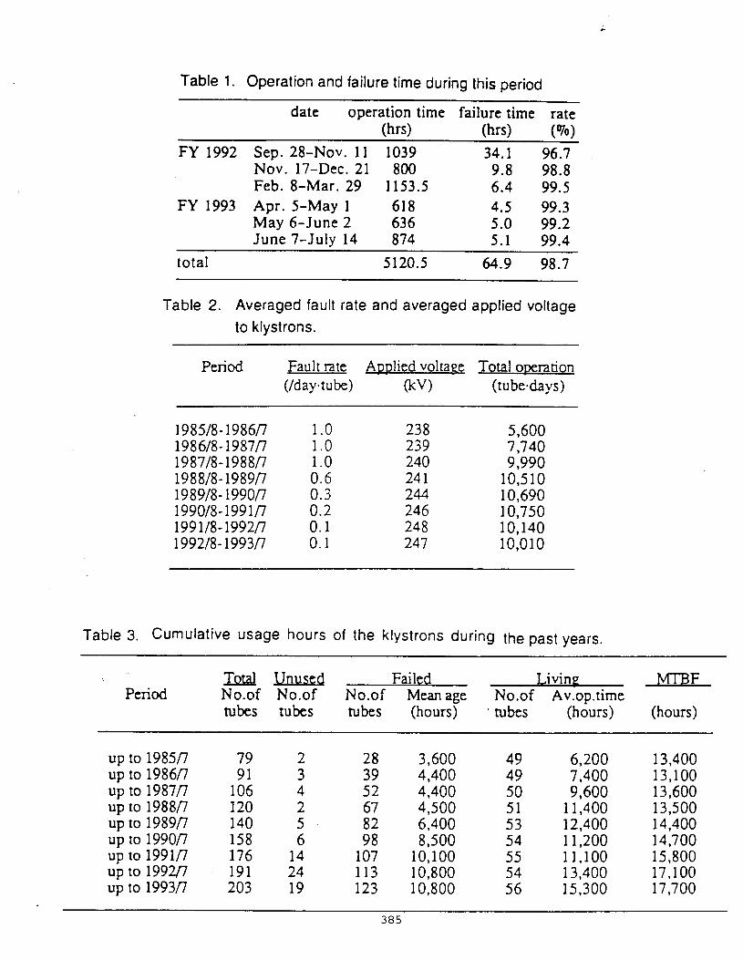
*
Table 1. Operation and failure time during this period
date operation time failure time rate(hrs) (hrs) (Vo)
FY 1992 Sep. 28-Nov. 11 1039 34.1 96.7Nov. 17-Dec. 21 800 9.8 98.8Feb. 8-Mar. 29 1153.5 6.4 99.5
FY 1993 Apr. 5-May 1 618 4.5 99.3May 6-June 2 636 5.0 99.2June 7-JuIY 14 874 5.1 99.4
total 5120.5 64.9 98.7
Table 2. Averaged fault rate and averaged applied voltage
to klystrons.
Period Fault m~e ADDlied voltage Total oxration
(/day .tube) @v) (tube. days)
1985/8-1986fl 1.0 2381986/8-1987~ 1.0 2391987/8-1988n 1.0 2401988/8-1989fl 0.6 2411989/8-1990fl 0.31990/8-1991fl 0.2 ;:1991/8-1992fl 0.1 2481992/8- 1993fl 0.1 247
5,6007,7409,99010,51010,69010,75010,14010,010
Table 3. Cumulative usage hours of the klystrons during the past years.
MM Failed Living ~Period No.of No.of No.of Mean age No.of Av.op.time
tubes tubes tubes (hours) ‘ tubes (hours) (hours)
UP tO 1985nUp to 1986~Up to 1987nUP to 1988~Up to 1989flup to 1990nup to 1991nup to 199Wup to 1993n
79 291 3
106 4120 2140 5158 6176 14191 24203 19
28 3,60039 4,40052 4,40067 4,50082 6,40098 8,500107 10,100113 10,800123 10,800
494950515354555456
6,2007,4009,60011,40012,40011,20011,10013,40015,300
13,40013,10013,60013,50014,40014,70015,80017,10017,700
385

Table 4. Cumulative status of klystrons up to July 1993 corresponding to the year of production. Unused tubes are those
which have never been used in the klystron gallery. ST6(stand-by) tubes are those which have been used in
the gallery and can be used there again.
Ycu of Mu Livine F~ cdil Fprodution Gtiodc No.of No.of No.of (STB Worbng) Av.op.[imc No.of causes Mean a=
“.
mks tubs mks e- c+ (hours) houm)tuks (ming window others) ( “U- (mk-houm)I979 oxide
(houm)4 0 0(0 00) ------ 4(2 3,902 15,608 3,902
1980 oxide 20 1( I 00) 3,657 19 ( 13 ; !1 9,030 175,606 9,242]?g~ oxide 20 : 1(100)11,277 19 ( II 2 6) 15,965 314,6111982 oxide 90
16,5881(1 00) 2.120 2 10,054 82,549
198310,317
ofidc 13 0 1(1 o 0 ) 14,170 1:1: ;~ 18,753 239,2051984
19,934oxik 13 1 0(000) ------ 12 ( 10 : 9,950 119,401
1985 oxi* 129,950
0(000) ------ 11(7 0 ;] 13,409 147,4941986
13,409oxide 15 h 1(1 O 0 ) 11,568 14 ( 13 0 3,524 60,910
1987 oxide4,351
u 7 0 0(0 00) ----- 7(5 1 1) 4,342 30,393 4,3420 [d 113m 5 ( ) 8,558 106 ( 72 13 21 ]0,783 1,185,777 11,187
Yw of. .
@ution GWC N%f a No.of (STB Worhng) Av.op.time No.of1~ Ftilcd
tiuscs Mm a~mks mks C C (hw) w Ow
1987 BI o 5(0 ; 0+ ) 27,857 1 1) 16,74a 86.391I 988 BI 2; 1 15(3 9 3 ) 20,393 :[: 1) 12,814 357,153 89,2881989 BI 18 11 ( o 10 1 ) 19,194 6(0 :1) 10,525 274,2841990 BI 18 ; 9(1
45.7.147 1 ) 12,568 3(0 1) 8,902 139,a17 4
1991 BI 15 a 5(0 41) 4,106 ; 2,843 26,216 11992 BI 12 6 6(051) 3,652 ;[ 8 0 : i ---- 21,913
td 90 17 51 ( 4407 ) 15,919 17 ( 13 4 ) 10,605 992,165 5
Id 203 19 56 ( 9 40 7 ) 15,262 123 ( 72 26 25 ) 10,758 2,177,942 1

Cumulative usage of the thyratron during the past fiscalyears
Period Total no. Unused no. Failed no. Living no. operation hrs
85/3 56 1286/3 56 48713 61 78813 74 1789/3 74 1590/3 83 2091/3 88 2192/3 91 2193/3 94 2194/3_.. --- ~lo4 (Jo> 25
95/3 126 (32) 37 (~3)
96/3 144(~)
o0257
10141720242727+?
44 KU275C5252525253 F175535353 -—-- ----——5 ~(i~) F24162(1J L488864 CX241O
6,8009,700
13,70018,20023,70028,90034,10039,20044300---d -——-49,60054,800

388

Hystron-Modulator System Performances
For PLS 2-GeV Linac
M.H. Cho*, J.S. Oh, S.S. Park,and W. Namkung
PAL, POSTECH, Pohang, S.Korea
(K&M Work Shop @SLAC, Oct. 1995)
K&wcHo-95

390

!
PLS/POSTECH-PAC9s
Main Parameters of Klystron
Parameters E-3712 S-5045
Operating Frequency (MHz) 2,856 2,856
Peak Power (MW) 80 67
Average Power (kW) 18 42
Pulse Length (ws) 4.0 3.5
Rep. Rate, max (pps) .60 180
Drive Power, max (W) 500 800
Beam Voltage, max (kV) 400 350
Beam Current, max (A) 500 415
Gain (dB) 52 53
Efficiency (Yo) 42 45
Micro-pemience 2 2
Manufacturer Toshiba SLAC
391[K&hVCHO-95Pj

n
0x-
rI ii
I
1:1 I
I ,I III —.—.—
I II
‘\
I I
I1
I ,[I~1
—— ———— , II
I!. ..—. .——— —————— —— , \,k $ I
!
1
——_—_ ~..—.,
m 7
——— —.——1
1
I I
1
,

PLS Linac
Main Parameters of Modulator
PLS-150 PLS=200
●
●
●
●
●
●
●
●
●
●
Peak Power (MW
Average Power (k~ @ 60 Hz
Peak Beam Voltage (k~
Peak Beam Current (A)
Max. Pulse Rep. Rate (Hz)
Pulse Width (~S)
- Flat top
- EswPulse Flatness (%)
PFN Impedance (Q)
Pulse Risetime (ps)
Pulse Falltime (~)
150
58.2
350
420
60
35
6“57*=0.5
3.73
0.8-1.0
1.5-2.0
2008040050060
44
7“67
*“Om5
2.74
0.8~fm0
1.s-2.0‘

-—
PALIPOSTECH
Table 1. Operation Parameter Summary for Klystron-Modulator
Peak beam power 200-MW m- (400 kV @500A)
Beam vol. pulse width ESW: 7.5 psec, Flat-top: 4.4 ~sec
Pulse rep. rate 120 pps m- (currently 30 pps)
PFN impedance 2.64Q (5V0 positive mismatch)
Voltage stabilhation SCR, DC feedback& 5V0 De-Q’ing
Pulse transformer l:17(turn ratio), L1k:l.3pHy, Cst:69nF
Fhyratron switch Heating factor: 46.8x109,8.5 kA peak anode current
Wystron tube Drive power: -300 W, efficiency: 40Y0,gain: -53dB, peak power: 80 MW(currently running at 50 to 65MW)
K& WCho-95

.
~––––-... —-———.—.—— —— A_______ .—— ———. —— __ ._,
r ——————_ IIII REC. DIODE
I
FILTER CHARGING DE-SPIKING 14 SECTION 2
CHOKE lNDUCTOR CHOKE PARALLEL PFN L PFN—
=
I Ill+
III
‘dI KLYSTRON i
Ii III III I
IV8 III I~TRIM~‘; ? ‘
E.-.::: ‘“:-:X-FMR ?;—(1:17)
mr–lII
I Ill i
DE-UING
il T [Wl
. ..-
DIVIDER*
! ilk *li
I PM~O A~ELERATOR LABORATOR?
T~LESCHEMAmC MAaRAM
2~MW MOWLATOR
AND - KLYSTRON

<
n
uaz
d
m
. ... .......... ..............
,,:. .::..................._,
..............................................................................................................................................................................................................................................................
-––-\\––.~nl
Ill r ‘II 1 IA

LINAC PAL
PLS-200MW MODULATOR& 80MW KLYSTRON FRONT VIEW
w
WGNTOWER
~ DE-O RESISTOR
COOLING FAN

LINAC PAL
THYRATRON MAIN PARAfiflETERS COMPARISON
mmmHeater Vett~ (VAc)Max. ~ Current (A)Reservoir Voltage (VAC)Reservoir Current (A)Minimum Heating Time (mlntiee)Max. Peak Anode V, foward (kV)lMax.Peak Anode V, inveree (kV)Min. ~ Anode Supply V (kV)Max.Max.Max.Max.Max.Max.
6.0- 6.6802.5- 6.020155q45.9)502
5.9 w6.7903.0- 5.5401550N/C
10
6.0 u 6.6906.0- 6.671550505
Peak Anode Current (kA) 1~8.5) 10 10Avor~ Anode Current (ADc) 8(7.64) 8 10titt~ Faotor (pb = opy x lb x prr ,xl@ 30q46.8) 400 Nm
An- C~~t Rateof Rise (Wus) 50Anode My Time (us) 0.3lime Jl~er (ns) 2
me val~s given in parenthesis are maximum
16 100.4 0.3510 10
operating rangewith the 200 MW modulator
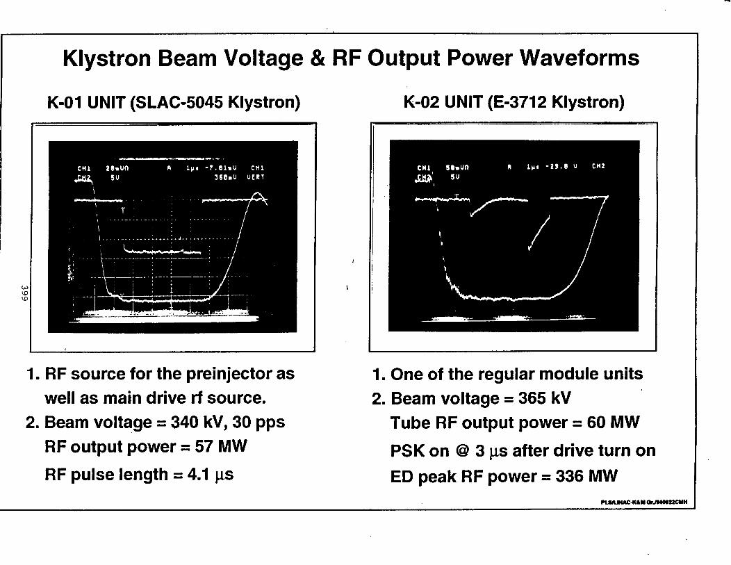
.—
Klystron Beam Voltage & RF Output Power Waveforms
K-01 UNIT (SLAC-5045 Klystron)
I ‘
1. RF source for the preinjector as
well as main drive ti source.
2. Beam voltage= 340 kV, 30 pps
RF output power= 57 MW
RF pulse length= 4.1 US
K-02UNIT (E-3712 Klystron)
r—
I1.One of the regular module units
2. Beam voltage= 365 kV
Tube RF output power= 60 MW
PSK on @ 3 ps after drive turn on
ED peak RF power = 336 MW
.
,-

0nu
-
0>
c0L
u
-
Y
.
7“4 t
1
IL -“7.
I 1 t
—.
I.
400

I PLS Linac PAL I
ACCUMULATED KLYSTRON BEAMVOLTAGE(399kV) WAVEFORMS
Wl~ OUT DE-Q’ING(UPPER TRACE)& MTH DE-Q’ING(LOW ER TRACE)
-38.
,“Q ~1’.’. .
,. ’.’
I
. . . . . . .
,..... .. ................ .
11
. . . . . .
. . . . . . . . . . . . . . . .
. . . . . . . . ..... . .
● ✎
I
-2. Q8US l~s~’di’.’ ~-—— --——— —-— ---— 7.92P%
401
.
,-
I
! I I I I I I I I I
II +I
Tr0
I 1 I
1
// +
\\
I F“ / I
I 1’ \
— a
1 / /
I I1 e,, , +
/ I I
m1/
,,I
,, i
~. I z
ao 0
402

.,
PARETO CHART OF PLS KLYSTRON MODULATOR SYSTEM
e 720.3
*OOA 229.5
1
I
I(48)
_ Amplitude= 115I
1
H
@@@@@@@@@@o@ @@@
@ CB Trip
@ Kly. Vat.
@ Fan
@ Thy. GIC
@ Core Bias Curr. LOW
@ Key SW
@ DCPS overvoi~
@ Msg. C“rr. LOW
@ Core Bias Curr. High
@ SCR Gate Hold
@ Rear G/Hook
@ Msg. Temp. High
@ SCRAC Over Current
@ Msg. Flow Low
@ Others ‘
@ ● Down Time (Hr)
Fig. 3 Pareto chart of the system fault statistics. Numbers in the x-axis indicate type of faults, circles indicate down times, and the bars indicate
accumulated interlock counts. Grey colored bars and circles are for the period of September 1994- March 1995 (4752-Hr), and the black
colored marks are for the period of April 1995- July 1995 (2688 -Hr).
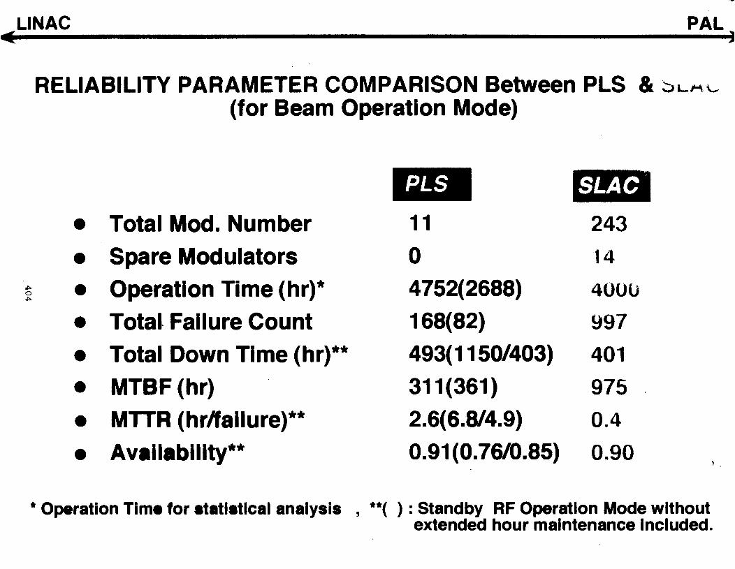
—
LINAC PAL
RELIABILITY PARAMETER COMPARISON Between PLS & ~LA~(for Beam Operation Mode)
Total Mod. Number
Spare Modulators
Operation Time (hr)*
Total Failure Count
Total Down Time (hr)**
MTBF (hr)
M~R (hrfiallure)**
Availability**
11
0
4752(2688)
168(82)
493(1 150/403)
311(361)
2.6(6.W4.9)
0.91(0.76/0.85)
243
14
4UUU
997
401
975
04
0890●
)
* Opration Tim@for statistical analysis , *’( ) : Standby RF Opration Mode withoutextended hour maintenance included.

LINAC PAL .4
MAJOR MODULATOR TROUBLES AND IMPROVEMENTS
1
CB Trip
DCPS OvervoltageSCR Gate Hold
Thyratron
Related Troubles
IKlystron Vacuum I ~ I Klystron
Core Bias Current
Low & High
I Related Troubles I
1
Switching Noise I
Related Troubles
Ranging
or
Command Charging
Short pulse
Processing
Noise Filtering
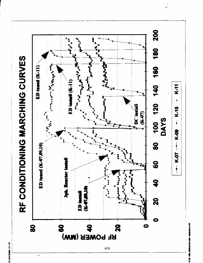
o0w
o*F“
\
Y
s
/’
oo
4.06
3iz
.

,—
.. .
1. Klystron Mdulator SyS~@;= Total c 1 + 10* unib u- normal ~Uon.=System petiance ~ dl des[~ quirements.- Over 140,~ of toW H. V run Urn. W 11 Wystrons.- No ser~ous WMical ~ or fa~~ obsewed.Ao
“ 2. Systemb wli~ A~sis;- -90% of sys~% availaffll~ for beam opera- md.- Most of failures are due to We tiyratin tiw.
3. Others;- R&D for compact and efflciont Klystron m~- R&D for systemk relie~ improvement u~y. 7
K&WW5

=YSTRON-MODULATOR SYSTEM PERFO~CESFOR PLS 2-@V L~AC*
M. H.~o, J.S.Oh,S.S.Park andW. NamkungPohangAcceleratorLaboratoy,POSTE~
Pohang79@784,Korea
O.~STUCTThe PLS 2-&V finac employs 11 units of high-power ptised Mystrons (80-m as the main RF sources. The
matching moddators of 200-MW (400-kV, 500-A) can provide a flat-top ptise tidth of 4.4 ps with a maximum ptiserepetitionrate of 120-Hz at tie Ml power level. For a good stability of electron beams, the ptise-to-ptise flat-top voltagevariation of a modtiator requires less than 0.5Y0.k order to achieve this god, we stabfized high-voltage charging powersupplies within l“Aby a phase controlledSCR voltage re@ator (AC feedback). h addition, we employed DC feedback,which petiormed well tithin 0.5%variation of the PFN charging voltage. In this paper we analyzed the over~ machineavailability and tie system fatit statisdcs during the PLS (Pohang Light Source) commissioning operation. During thisperiod the availability was -9070 for the case of 24-hr maintenance mode tith 2-shifi work and the availability droppeddown to -75Y0for the case of day-timeonly (44-hr per week) maintenance mode. The most frequent we of static fadtwhich require the attendance of a maintenance crew has been identified as main circuit breaker (CB) trip due to theabnormalbehavior of thyratron switihes. For the improvement of the system avdabfity the SCR gate hold interlockand the slow start of the DC high voltage together with the automatic remote reset of tie static fatiti using the controlcomputi have been added during the ’95summermaintenance shutdown. PLS is now in the norrnd operation mode forthe beamline user se~ice (started horn September 1, 1995). In this paper, we dso presenfi the key features of theNystion-modulator system and the short term preliminary re~t of the avdabfity analysis &r the system modification,approximately 1-month period.
I. INTRODUCTIONPLS linac has been injecting 2-GV electron beams to the Pohang Light Source (PLS) storage ring as a part of the
ring commissioning operation since September, 1994[1]. The linac klystron-moddator (K&M) system has been inoperation well before the ring commissioning, and the toti accumtiated high voltage run time of the oldest unit hasreaehedbeyond 15,000 hours as of Sep. 1995[2]. The K&M systems are normdy operating in 70 to 80°/0of the ratedpeak-power level to avoid the multipaetering phenomena occasiondy occurring in a random fashion inside thewaveguide networks and accelerating structures of the finac system. The sum of W high voltage run time for total 11K&M systems installed in the PLS finae, is approximately 158,000 hours.
h this paper, we review overall system performance of the high-power K&M system. A special attention is paid onthe analysis of W failures and troubles of the K&M system which affected the hnae RF operations as well as beaminjection operations for the period of September 1994 to Jtiy 1995. During this period, the machine has been in theoperational mode for total 310 days. Summer shut-down and tie schedtied maintenance shut-down time are excludedin the analysis.
II. K&M SYSTEM O~RWEW~ PE~O~CE
The key features of the K&M system design include the 3-phase SCR controHed AC-line power control, resonantcharging of the Pm, resistive De-Qing, end-of-line cfipper with thyrite disks, pdse transformer with 1:17 step-up turnratio, and high power thyratron tube switching. me major operational parameters of the PLS-200-W klystron-modtiator system are listed in Table 1 and the system schematics are shown in Fig. 1. The details of the system designand performance characteristics are described elsewhere [2].
The shot-to-shot beam voltage stabifity is controHed by (l)the feedback of the DC high voltage from Pm to SCR
primary input voltige control and (2)the resistive De-Qing. SCR DC feedback provides less than *0.5Y0 fluctuation, andadditional De-Qing stabilizes the beam voltage better than +0. lo/o fluctuation level. Fig. 2 shows the sample traces ofthe beam voltage accumulated more than an hour which exhibits less than +0. l% fluctuation.
For the fault free stable operation of the system, the thyratron tube is one of the most important active componentswhich require continuous maintenances and adjustments. The thyratron tubes which meet the PLS-200-~ system
408

I
specifications are listed in Table 2 together with their specifications. ITT~-303 and Littofi-4888 are installed in oursystem, and the performance evaluations are underway. Recentiy EEV/CX- 1836A has been installed dso for thecomparison. This effort is initiated to improve the system from the frequent occurring faults (see Fig. 3) caused by theirre@ar recovery action of the thyratrons, which strongly depends upon the reservoir control.
There are three types of system interlocks, namely dynamic, static, and personal protection interlocks. All the staticfault activation is initiated by the relay logic circuit, and the dynamic fatits which require a fast action response areactivatedusing the electronic comparator circuit. When the system operation is interrupted by the static fadt, it can berecoveredeitier by the remote control computer or manurd reset. However, we have been performing dl manual resetstill Jdy 1995 for the purpose of the experience accumdation, such as to find the type of troubles and system bugs whichcan provide the idea of the system improvement. The statistical analysis of the machine availability presented in thispaper is based on the operation method of the manual reset by the maintenance crew only, without using the remotecomputer contiol. On the other hand, in the case of dynamic fatits, the system recovers automatically without the helpof the control computer when the condition returns to a normal state.
Table1. Operationparametersummaryfor klystron-moddator. Table 2. Comparisonof the thyratrontubes.Peakbeam power 200-MW max. (400 kV @500A)
ITEM ITT Lifion EEV CX-Beam vol. p~e ESW 7.5ps, 4.4ps flat-top
F-303 L-4888 1836Awidth Heater(Vat/A) ma 6.6180 6.7190 6.6190Pdse rep. rate 120 pps mm. (currentiy 30 pps)
PFN impedanceReservoir (Vdc/A) mm 6.0120 5.5/40 6.6/7
2.640 (570 positive mismatch)
SC~ DC feedback&5% De-Peak anode @V~)Jor 50/15 50 I 10 50/10
‘oltage ‘tabmdon Q’ing Peak anodevol.@~ inv 50 tic 50
Pulse transformer1: 17(turn ratio), Avg. anode cur.(A) ma 8 8 10L1~:1.3~,C,t:69nF
minDC anode vol.@~ 2Heating factor: 46.8x10⁹,
10 5Thyratron switch
8.5 kA peak anode current Heating factor (xlO~ ma 300 400 tic
Drive power:-300 W, dUdt ~ps) ma 50 16 10
Wystron tube efflciency:40Vo, gain:-53dB, peakpower:80165 MW Anode delay (ps) ma 0.3 0.4 0.35
(Currentiy*g at 50 to 65MW) Trigger jitter (ns) ma 2 10 10
111 SYSTEMAVMMILITY STA~STICSSince the completion of the PLS 2-OeV Enac installation in December 1993, dl the K&M systems have been
operating continuously except schedded short-terms and long-term shut downs. Table 3 shows the totrd accumulatedtimes of Mystron’s and thyratron’s heater operation, and the high voltage run. Sum of the high voltage run time of eachmodtiator has reached over 158,000 hours, and the experience accumdated so far provides the valuable information forthe system’s stile operation. Fig. 3 is the Pareto chartof the total system’s static fadt count data collected for the periodof September 1994 to March 1995@y colored) and Apd 1995 to July 1995 (dark colored). Net operation days duringthis period is 198 and 112, respectively. As mentioned in the previous section, the reset has been done by themaintenance crew only, and at the most of nighfi and weekends during the period no extra maintenance work has beenperformed except the ring injection operation time. Therefore the down time for the circuit breaker (~B) tip whichoccumed the most fiequentiy is unusually high among others. Other fadts, such as fan(~) and key switch(@) are duemairdyto fatity components, which no longer occur in any appreciable numbers afier the replacement. Troubles relatedwith tempreture and coolant flow are due to the fati~ in the cooling pump station.
Machine availability analysis has been performed based on the data using the techniques described in detail inreference [4]. The resdk are summarized and compared with the SLAC’s in Table 4. The MTBF stands for the meantime between failures, and it is cdctiated by dividing the sum of the accumtiated modtiator run time with the total fatitcount ~TBF = N* TO~C). Them (meantime b repair, which is equal to the total down time divided by total fadtcounts, Mm= TD~C) is rather longer than the SLAC’s due to the extensive inspection work of the entire system forthe trouble shooting as well as crew training for the system maintenance. Especi~y, the lack of the experience on thethyratron operations and severe EM environment have contributed a !ot for the longer MTTR.
Approximately 76% of the machine availability (A = l-MT lR*FC~O) has been obtained with the maintenance work
409

of 44-hr-per-week. However, during the beam operation mode when the maintenance crews are standby, approximately9l% of availabili~ has been reached even without a standby K&M system. It indicates most of tie system troubles arenot so serious, and in many cases they are easdy recoverable.
IK COMME~S ONSYSTEM TRO~LESThe most frequent system fadt is the circuit breaker (CB) trip as shown in Pareto chart. This is due mainly to the
problems in thyramn recovery actions which require elaborate resemoir ranging. Thyratron tubes of F-303 and L-4888require rrmging adjustment (see Table 2). According to our experience, they are changing in irregular patterns such thatthere exist no norrnrd patterns or pre-syrnptoms which can be used for the preventive maintenance. Once it is out ofnormrdoperating point, there occur self-fire, firing miss, or slow recove~. The CX-1836A thyratron tubes require notso delicate ranging according to the manufacturer’s specifications, and recently we have installed one unit for thecomparison. Klystron tubes dso showed an intemd arcing causing the vacuum pressure trip in a random fashion (see@ in Fig. 2). When this occurs in a row, we codd recover to the norrnd operation her performing the short ptiseprocessing (with approximately lps ptise width) for more than one day. However, this me of fadt showed pronounced-- .decrease as the run time accumdates.
Table3. Accumti u times (m hours) summary of the PLS2-@V Linac’s K&M systems (toti 11 sets); data co~ected onSeptember 22, 1995.
Unit No. Wmtirne Kly. heater Thyratron
MK-o 1 14,432 16,634 16,852
MK-02 .17,107 924 (*1) 16;454
MK-03 15,807 16,568 18,667
MK-04 14,973 16,523 16,747
MK-05 14,312 15,908 16,422
MK-06 14,296 15,453 6,343 (q)
MK-07 13,157 14,664 15.455
MK-08 14,123 15;473 15,397
MK-09 13,058 14,518 14,518
MK-10 12,890 14;333 1,547 (“3)
m-n 13,033 14,447 8,114 (w)*1) Wymn replaced tier heater run time of 18,883-hr due to
the focusing solenoid trouble.*2) Thyratrons repl=d with L-4888 due to the fdure of
F-303 (after -9500-hr We).*3) Thyratrons repl~d F-241 to F-303) after -8,000-br ran.
Table 4. Comparison of the K&M system fault analysis basedon the data for the period of September 1994- March 1995.
I I~M I PLS*2 I SLAd41 I
I Number ofmoddators, N\ II I 243 ~
Spareno. of modtiators 10 1141, 1
Operation time @)*l, TO 4752 4000
Total fdure counts, FC 168 997
Total down time ~), TD 493 (1 150) 401
~F ~) 311 975
m @/Fdwe count) 2.6 (6.8) 0.4
System Avtiab%ty, A 0.91 (0.71) 0.94*3
1) Operation time for the Statisticalanalysis.2) Numbers in ( ) indicates the standby RF operation mode
without extaded hour maintenance work (ody 44hrlweek).
*3) Standby spare unit included
Other fiquendy occurred troubles are caused by the corona discharges. ~ey occur when bad contacts exist in highvoltage component, especirdly for the componens which are connected by the spring type clamps. It has been founddso that even a small corona discharge disturbs the ground potentird, which are configured to have a single point groundconnection inside the modtiator, causing noise intefiaces in digiti displays andor SCR phase controls. Occasionrdly,this kind of Em dso affecfi LCD type displays of the nearby electronic equipment without affecting the performance,which became one of the normal checkpoints for the system performance.
K SUWRY
It is approximately l-year since the PLS 2-OeV Linac has started its operation. We have analyzed theklystron modtiator system’s performance record for the period. It is obsemed that the rehabilip of klystrons iswell over our expectations compared with other components in the modtiators. The life time of thyratron tubes appearsto be reasonable except the occurrence of infant failures. However, the major improvement is necessary for the resemoircontrol which is the main source of system troubles. The machine availabifi~ statistics of the K&M system for the beamoperation mode (~icdly 2 operators are on-duty) is cdcdakd to be over 90°/0. It appears to us that here are still lots
410

of rooms for the improvement tiward the availability more than 95°/0with proper choices of the protection circuits andcontrol logic. During the period of May 1995 to Jtiy 199j we have modified our OCR (overcurrentrelay) interlock notto interrupt main CB but SCR gate (with static fault action) as an attempt to reduce major source of static fatit. Duringthe period no system damage has been occurred, and we now added remote reset control in the case of static fadt. Justone month old statistics shows an excellent system’s availability. Long term performance restit will be reported as weaccumulate enough data.
Fig.2 The flat-top ripple and the cumulative (>1-hr) W. MFEMNCESstabihty measurement of the klystron beam voltage with [1] W. Namkung, “PLS 2-GeV Linac,” Proc. 1994DCW fdbaek and De-Qing. Tektrotix DSA-602 signal International Linac Conf., Tsukuba, Japan, Aug. 21-26,andwer is used.
—J —
lr] ‘d“.Wg,...::.:; ,,.m1, :..
pp.14-18 (1994).2] M. H. Cho et. d, “High Power Microwave System for PLS-
2-GeV Linac,” Proc. 1994 Intemationd Linac Conf.,Tsukuba, Japan, Aug. 21-26, pp. 418-420 (1994), M. H.Cho et. d, “Design of 200-MW Pdse Moddator for PLS2-GeV Electron Linac,” Proc. 3rd European PhcleAcceleratorConf., BerYi Germany, VO1.2,pp. 1591-1593(1992).
[3] I. S. Ko et. d, “Control of PLS 2-GeV Linac,” Proc. 1994Intemationd Linac Conf., Tsukuba, Japan, Aug. 21-26,pp. 825-827 (1994)
[4] A. R. Donaldson and J. R Ashtoq “SLAC ModdatorOperation and Rehabfity in tie SLAC Era,” IEEE Conf.Proc. 20th Power Modtiator Symposium, pp. 152156(1992).
Wl AC~O~EDGEMENTThe autiors would like to express sincere hanks for all the K&M Group members, whose names are S.W. Park, S.D
Jang, S.J. Park, Y.K. Son, K.T. Lee, and S.H. Kim, for their devoted work for the Klystron-Modtiator system of the PLS2-GeV Linac.
Fig. 1 Schematicdrawingof the ~stron-Modtir vstem
CHARGING CHARGINGEOLC
4a0V D.c. DIODE
T V* fll ?7~~ ,:.;3hPOWER . ;:
&:::::
t t
lHYRATRO
TRIGGER THYRATRON
INPUTGRID
N 2 huql
120V14
60HZ
411

PARETO CHART OF PLS KLYSTRON MODULATOR SYSTEM
200> I
1@ CB Trip
@ Kly. Vat.
@ Fan
@ Thy. G/C
@ Core Bias C“rr. Low
@ Key SW
@ DCPS Ovemolt.
@ Ma,. C“rr. Low
@ Core Bias Curr. High
@ SCR Gate Hold
@ Rear G/Hook
@ Msg. Temp. High
@ SCRAC Over Current
@ Msg. Flow Low
@ Others
WO Downtime
Fig.3 Paretochartof thesystem fault statistics. Numbrsin thex-=is indicate~eoffaults, circles indicatedowntimes, andthe bars indicateaccumulated interlock counts. Grey colored bars and circles are for the period of September 1994- March 1995 (4752-Hr), and the blackcolored marks are for the period of April 1995- July 1995 (2688-W).
!
SLAC MODULATOR RELIABILITY
J.ASHTON
413

I!
!
I.,.,
I
. . . .
. ~urn~r of Intervcn(ions
~pmn W@ng
M~ Pm TuningReplace Filment RTM
Repbce Fihent ~Repbce BIA=
Repkce T-mRepbce ~ RTMRepkce W MCM
! f t i 1 1 !
:.:<.x..,:.:.x.:,:< .:.::.:.:.:.:.x ., . . . . . . . . . . . . . . . . . . . . . .. . . . . . . . . . . . .. . . . . . . .
. . . . . . ..- . . . . . . ...>. . . ...2.%...A:.*.*.......... . . ....~....~<..<.... .... ... ..... . . ...... , . . . . ...................... . . . . ........... . ,/. . . . . . . . . . . . . . . . . . . . . . .
...... .... ........................................................................................... ............<........<.>..>>.:.:-:-...:(... <~. . . . . .....%...$.+)~$.+:~.:.:.y#,.................... .....4<.. ....8 . ... ..a. . . . .. . . . . .. . . .. . . . . . . . . . . . .. . . . . . . . . .. . . . . . . . . . . . . . . . . . . . .
t8* 8)8
................................................................. .....,.,............/...........8~.,......................
~.:.:.:.?..:.:<.>.... till’
!
. . . ., ..................................................................... ..... . ...... ....... . . . . . . ..... ..... .......................................... . . . .... .........,.... ............ .. ..... ..... ... . . . . . . . . . . . . . . . . . . . . . ... . . . . . . . . . . . . . . . . . . . . . . . . . . . . . . . . . . . . .
Time in lIours
...................
I I “11 lBl@●. <. ..)...* i

../
{“
.
LP“~
.\, .. . . .
‘.w“”.”-.”)
.’... : .. .’.. .. .. . . . .. .-. .
- . ” . - . . --, -------- “... -—-— -.?—.-:& -..: ,—-!- -------
I ..- \...{
l=..c-,. ,.. . I., , ..-- ...-— —
415
..,

...-. . . .
,... -
-’00
I
\
.-.
. L
416
I

.
MODULATOR PM SIGN-OFF LIST
SECTOR _ DONEBY_________ DATE
STATIONS.
1. INSPECTION 1 2 3 4 5 6 7 8
A. GROUND HOOKS
B. DOOR LATCHES& INTERLOCK SWITCHES
C. LAMPS
D. FANS
E. PFN COILS & STRAPS
F. MAIN CONTRACTORS
G. OIL LEAKS
H. BNC FEED-THROUGHS
~ 1.BLEEDER RESISTORS
J. SCR ASSY & RESISTOR STRAPS
K. RFI FILTERS
L. TRIGGER CHASSIS
M. TZO & EOLC CONNECTIONS
N. TRIAX & TANK SOCKET
Il. OPERATION
A. K-28 SET
B. SHUNT TRIP
C. FAULT STEPPER
D. K-14 (Min. 2 Sec Delay)
E. TUNE PFN
F. THYRATRON RESERVOIR SET
G. HIGH VOLTAGE STABILITY
H. NOTIFY MCC OF COMPLETION
.,Paae 1 of 1
417

...
Reset Relay tik-upReset M CB
R&t lnmlwk
Rcscnoi Yolhge AdjustRcpbcc hlse Cable
Rcphcc ~ym~nBm Vol~ge Adjust
Repbu my MverRephe R~ay
Mod T~ h
Repkcc ~bg CompRepkce Tri~a Unit
Connations & Conn=@n
Repbce ~W Cornp
Cl=n P~x Cable
Repkce FW
Fan bbIa
Reky Problem
T-20 Adjus~ent
Repair COR Bti
Rep~m Pm Cap
Remove Gnd Hook
~larnent vol~ge Adjust
Chnge Tri~er SU[US
Fm Wfi ~blem
R~nnwt ~lse Cable
Repbce WA PS
Repti ~ Rfifier
king ln~~’~tion
Repair my Grid Circuit
“ Jitter lnv~tigation
~yratron Klixon Trip
Replace my Gfid Chuit
Rcpair T-20 Tap
Clca~cpl~cc VM.ac
.’
Numhr of lnfervcn(ions
.
lIIJ
1111
I* II
1 ##1
Itll
lets
8118
9 *I,
8111
I* II
Ist$
II::
*11,-----
.,, ,call,
1#, *II,
I*, lBa,
*I, 18, ,
18, ,,
I
-- ●
I
I
I
t
I
1
1
I
II
:
9
aI
a1
I
8
I
I
I
I
t
I
t
t
t
I
t
I
I
1
I
I
I
t
t
I
1
I
I
I
I
8
I
:
I
I
*
I
I
*
t
t
8
I
I
1
1
I
I
I
t
I
I
I
I
1.
I
I
I
1
1
I
I
t
I
t
sI
I
t
I
I
[
8
I
I
a8I
1
t
I
I
I
t
I
1
I
0
I
1
I
I
I
B
I
0
t
I
11 Itll
I Im #l,
II III*
I 11 all
II 1111
II 8811
I I;ttl
tl 1811
1. 11811
#l ##I:
01 9111
II 1111
*I 11:1
‘1 I Ills
II 1118
II 1111
II lB#l
lb till
11 1811
I* 1111
Ii Ills
1.! s:,,11 Iltl
al 1111
11 1881
II 8:81
IS 1s11
II Ill:
1$ 1111
II 1018
88 1181
et BI1*
*# 1111
II 1181
II tlil
18 Ilsn
al 1111
II II* I
II 811:
II 8111
11 Ill}
II Ill:
II 8118
@ 11:11
Is 1111
al tall
II :118
II 8111
15 Ittl
It till
11 Iglt
11 Ill:
11 1s11
18 8111
I Itttlin 1881
II 1811
I 11s1s
II Iltt
#l 1888
II 1811
II IllsII 111:1’ 1 I 1.81
:1aI
11\IoIIt1t1I*8I1#Ia#I1I1I1
I1
1
II
vI1
I
I
1
t
1I
oI
I
I
It1
I
I1
II
I1
I
&
. . 418 Time in Hours

,.
.-. .
,:[. .
!
.,
,;
(
r
0,.<0-.>..
,-
3— “---’.-
0“ Qb 0
c
. .
419

,..,., ,, ,, ~,,,.; .,. ,, >.” .,,.
.,,
1
T=~ I :Avtilabili& of SLC ad Mduh~r Systims.
1991 19W 1993 94/560 120 120 120
w 5568 57% 65B
06 0.818 0.8B 0.794
0:884 0.829 0.849 0.863
O.w 0.94 0.92 0.991.
.,.,,,, ,,,,.,’
.,, ‘, J
,.

,,, ,, ,,, , ,, ,, ,, ,,,,., ,. ,,, .,. ,. ,’,,,., ,,
,,.. ,”’,, .,,
., ,,,,,
TNLE ~: Sys&m md Mdti~r Dam for Fom Rms.W Sys&m 15 Ctitid
,, . ! . .,.,, ‘.,
,.s,
21,W
5.33675373167
0.%529*707
0.4%
0.855
21,840
3.27e5
437
203
O.m50.0
750
.4a
0.991
Sys@m “ATTw/ Sp~s 0.931 not applicfile
.,.

—--
.
CONTINUING CONCERNS
Circuit Breaker Trips
~cient Interlocks
~e~ing Thyratron Resewoir
Pulse Cable Mortality
Contaetor Lifetime.

SLAC
SLAC-PW-95+909May 1995
MOD~ATOR AV~M~~ ~ WACT ON SLC OPEW~ON*A. R. Donaldson and J. R. Ashton
Stiord Linear Accelerator Center, Stiord Universi~, Stiord, CA 943@ USA
h 1991, the Stanford Linear CoWder (SL~ o~tiwith diverse accelerator systems, at ~ avtiity. b
the more auspicious 1992 and 1993 runs avaihbflityimproved to over 80%. For the 94@5run, the aafiwwas h about80%.Ignoringthedectic--lerator, thiskussion ti assess the dependenceof tie SLC on there~abifity and hence, avai~blfity, of 244 Mystronmodtir systems thatprovidepower to the machine’sbunched-particlebeams. ~ystron modtir a-fitymustbe 99% for the a~lemtor to functionat the 75%level. Fortunately, an excess of modtitor~ystronsprovides some redundancyan& therefore,Wows someHom tim thequirement thatM 244 Sy-s performsimultaneously. There are, however, 15 specificexceptions. They populate strategic positions at theinjector,damprngMgs, d positron-on ~ of theacwlerator complex. These, systems-without-spares,direcdy Muence ov~ ae~lerator av~bfiity. TheirActited avfifity as an ensemble is 90%, but byc-they haveopemtedatup to99%[1].hdivi-y, a*ction can tig an experimati programto a MLThe discussion includes a description of sevedimprovements to inmease future afibfity for themod- sy~
hjector StadonsSector1StationsN&SDampingRings
mm comeSL~ CoredSRTL Cd
Sectors 2 to 18 Stations*tor 19 stationsPohn So-
e-To Target Stado#e+ Awl~ S_n2
*m 20 stationssectors21 to 30 s~tionshergy to SK ArcsEnmto~
55
111
1357
11
:0
1.151.15
32.8343
30.s3150.236554746
Toti-Stadon aunt m1 kdi~ the maximumpossibk energy @basetigned)and does not include1- due w
15degree offset for BNS Dampingoverheadfor energyf~mod- down for maintenance
~Y~S down for main~nance.2 kdim~ stions which mmpress the beam but add noe- gain.
L MODULATO@YSTRONDEPLO~
The linear accelerator presenfly uses 244
~my- stions ~m 1991 ody X3 stations m-). From Table I it is tiost apparent that SK hasmom modtirs than n- for the rquired detectir
energy. This dews modulators to be repaired bysubstituting operatio~ but off beam mtitors to avoidbng repair k At any given time there may be as many
as 14 m~ av~le as sp~. However h is not aunived situation, and them are 15 critid mod-
(indicated in bold type) which do not have substitutes,hen= their critid tignation.
Table U offers the ~M@ons for the Mystrokmodti M. The mod-r ope~ at high voltage
and high curren~ conditions that essenti~y stresseHc componmk
3.5350414150120
6*41:15
;:54
FvA
w (max)kVA
TheSLCmust operate at 120 W witi a very highdegree of reliabtiity and on a continuous basis.
Fortunately, we have a modest ex~ss of m*or-Mystron systems which allows some measure of
-daney, and hence some fi~m fim the ~that d 244 m~myti operate simdtaneody.
The modrdator logbook for 1991 through 1995 W=
potiinto a~inorder todpthereMfi~and hence avtifity of the modtirs. me log books*O recorded station problems associati with them-tor computer interface, Mywn (which inckti ti
water, and -urn problems), ~wlerator s-ture and
waveguide problems allied with vacuum and waterinterlock Uystron& magnet- and600 Vacvariabk
~ork ~ by b ~~m of firgy m- DE-AC03-7@~515voltage substadon operation. The ~ was design~ to
‘,
423
Presented at the 16ti IEEE Pa&k Acceler~r Qnference (PAC g5) d Znti-.od bnference on High Ener~Accehramn, Ddh, T=, Mq 1-5, Z995

.. . . . . -..
revd specfi modtir problems and the ~uacy ofthose problems. Prior to this @ysis these revelationsexisted as ody anecdoti reco~ections among themodtitor cognoscenti, the data had not been quan~a
aardingly it mtidn’t be used to provide evidence forimproving the re~i of the m~
For five y- of ~ysis, we tie two approaches.First we compare hours of SLC opetion and mod-problem counts to W* and plot m- tie to fd-
- for tie tious m~ componentsas partofanenti system.Seco~ we * W of there~fity *combmeih dctite av~bfity, and offer theresds inTable~witharunbyrun summaryin TabkW.
The plots are dividd into * W, the “reset&adjustment”intervention,tie “x thenrun”occmce,and My the mmponentftiure situationthat~uiresremovaland repkmat of a componentor subsystem.Consider Figure 1, it shows the “reset & adjustment”m chartfor the modtir system. The x-ti dispkysthe -gory of-t or adjustment and the SW ope-gyear 1991,92,93, and %/5. The m in hours is on they-fi. These hours in~wte how often tie reset oradjustments occur, or require a technician to travel to theLinac g~ery. Th~ ms m not based on sbglemodtitors, but for the entire W stion Linac. Themod* operatedat@ W for 1991SLC run. The other~runswereat l~fiexceptfor afeww*of~W@on in N/5.
For the “Reset W ~“ category, the m axisindicates how oh innervation was qti to -t Wmain modtitor -t =er over four-t periodsofSLC operation. This circuit br~r can trip for sevd-ns, but the typid - involves thyratron Wh up~use of high reservoir voltage or a mtictioningthyratrom No-y the circuit -r trips ~ theov= currenttiti cWt W to open the primarycontactorfor the hv power supply. The plot indicatesthat some
improvement in W categ~ has ~ over the yesrs.The ins-on of a ferr*resonant voltage re@ator in1993may be responsible for this stight ia~ in mfor the %/5 - Unti the contactor or conbl ~heme areirn~ved or repw we ti contiue to be phguti bytin-m trips.
The five y= database contains 7537 nonsheddedintementions with 3,167 hours of tied _ time for
the 21,W hour SLC/modtior operating period. Thisoperating period can not be accurately m~ as thefront end (the fmt 13 modtitors) must always come on
‘, W* before the ~ of the modtitors down the k.
\
F“’’”J’m for-& Mjustments1
lm —~ 1
424

I
The 21,840 hour figure was determined by
approximate SLC o-g ~riods for 1991 through 1995which does not n~dy include tint end turn on timeor scheddti tnaintemce periods of lW than 24 hours.
Toti moddator-hours are tien 244 (243 in 1991)mod- times 21,840 hours for 5.33 Mega modtitor-hours of operatiom
Assuming that a constant fdure rate occurs fornonschedtied problems be on the operating hom and a
typid Poisson distribution for elecmonic quipmentftiure,
Modtitor System Ftiure ~ = 7537/21840 hr
Modtir System Ftiure Rate = 0.35 problem~ur,or a problem occurs about once every * hours for the244 uni~ configured as a “system.” This forces tiemodtitor @hnicians to enter the kc gtie~ almost
every three hours to corrwt a modtitor problem. Andthese dctitions don’t include the externrd problems, e.g.,vacuum and water interlocb for the MysEon and
accelerator waveguide, interface el=tronics or the600 v acUmty power.
The rnod~r “mm time to ftiure” is hen,
Mod& m= 5.33 M hr. /7537M-r m =707 hours,
which when considering the age of modtitors, thyratronftit rate, and reky control circuitry ~ms approx (thedatabaseerror codd be as high m * 5%).
The dction for the “mean time to rem with our
data gives,Modtitor _ = 3167 hr. /7537Mod@tor m = 0.424 hr. /problem
or the average m*tor problem (a repair or intervention)
~uires about 25 minuw to mrrecLThe ~ cdctiation of interest to the accelerator
operator and physicist is modtitor av-tity, or whenw it be depended on to wo& The rehbfity expe~ @veseve~ definitions for availabfity, we wifl use thefo~owing as it has been applied to other accelerator
systems.Modtitor SystemA~bfity = 1- @tiure Rate)m)
Modtitor System A~bZty = 0.854
~ wodd be tie “av&bMty” if there we~ no sparesfor the modtitors, however as mentiond atier thm are
up to 14sparesavtileandtheycanbeactivatedwithin12minutes to repb a fadty tmi~ Using the 12 minute or0.2 hour repair/repkment as the m, then incrm
the “av~bifity” to 0.931, a r-table increase thatverifies the advantages of tiundancy and av~le spares.
SLC operation is compromiti when we run out ofmodtitor -, or when one of tie 15 critid mod~rs
fails. The database contained 437 nonscheduled
indentions for the 15 critid modtitors with a toti time
for repair of 203 hours. We apply the above dctionsfor the critid mod~rs and hen com~ the data withthe entire ~mble of 244 modbrs in Table ~
TABU ~ System and Modtir ha for Four Runs.
244 System 15 Criti@SLC Openting Period 21,840 21,840 HrSLCm@@-hours 533 ti 327e5
No. of hterventions 7537 437Toti Repair Time 3167 203 Hr
System Ftiure Rate 0.345 0.020 PhSystem _ 2.9 50.0 Hr
Modtitor _ 707 750 HrModtdatorm 0.424 .M Hr
System “Av~fity” 0.855 0.991System “A” WIS-s 0.931 not ~ficble
The cnticrd modtitor vahte of 0.990 indi- tittick avfibfity was better ~ either of the above twodctitions for Modtitor System Avtidity whichoffered 0.854 for the no spm case, snd 0.931 for the
spares case, but it forebodm that the expecti av~fitywotid be no ktter b 0.854 since there are no spares forthe 15 critid _tors. We are Iuc&, or we give thesemod- more ~tion when @ti by the schedde.
Fdy, we tive at the comparison of Avtiti~ forSLC and the modtitor system. Table N offers this k
TAB~ N Avtilabtity of SLC and Modtitor Systems.
SLC Run Period 1991 lW 1993 94/5PRR @) 60 120 120 120
SLC Operating Hours 4008 5568 5736 6528SLC AWbtity 0.6 0.818 0.828 0.794
244 System Mod “A” 0.884 0.829 0.849 0.86315 Critid Mod “A” 0.990 0.994 0.992 0.991
W. CONCLUSIONS
SLC avaflabtity increased wtie the 15 CriticalModtdator Av~bMty waved about 0.99 indicating that
the modtiator system does not seriously impact SLC
performance. We continue to improve the re~fity of thesystem. Presenfiy we are ins~ng a device, an “anodereactor” that extends the Me of tie pti cable. It has
deffitely improved cable Metimes ti six modtirs where
it has been insti But even if ~ble Medmes improve bya factor of three “Av~tity” ody in~ by 0.970.
v. ~m[11 ~. ~ddsm and JR. Ashton, “SLAC Modtitor-on and Rehbfity in tie SLC a 1992 2~Power Mod- Symposium, ~ Confemu RecordCH3107B-152
425

I
RELIaL~ SESSION S~Y
J.C. Sheppard and A.R. Donaldson
The first presentation discussd Nystron production, fdure modes and tifetime of the SLAC5045. The m for tie 5045 Uystron is 50,000 hours. Previously published data onthyration Metime at SLAC is dso included. Thyratron tifetime in the SLAC modulators ismanufacturer dependent but for the past 3 years of SLC operation, the Mm has beenapproximately 14,000 hours.
The remaining addresses were by Linac system managers tim Lw~RN, ~~PLSmS~~, and SLAC. They presenti their modulator-~ystron system retiabifity andavtiabifity daa, as well as their fifetime data for Uystrons and thyratrons.
The data in the table below was tabulatti by the authors for comparison, but &ause of mis-interpretation, it may not accurately reflect the actual experience of the factities fisted. Plmseconwt the various system expem for accurate lifetime and avtiabflity data. k the “Period ofM-K Operation” row, we list the operating hours for physics research. The data extends fromone to six years of Linac operation for physics research.
The presentationsstressda common theme,thenecessityforpreventivemaintenance,systemmodularity,and desirabihtyofan integrat~diagnosticscheme toenablefasttroubleshootingand repair.
Linacbbomtory LW~RN PF~K PLsposmm SL~SLAC
M-K Linac Count 6 (1) 53 11 244
M-K Spares Count o 4 0 (2) 14
Period of M-K Operation[hr]
28,770 58,000 4,752 21,840
M-K Repetition Rate[pps]
100 25& 50 60 60& 120
~ystron Mm[hr]
22,000 17,700 >15,000 50,000
Thyratron Mm[hr]
12,000 >15,000 14,000
Moddator Mm[hr]
311 707
Linac M-K SystemAvdatity
0.978 0.987 0.910 (3) 0.931
Notes: (1) Count before the increase for ~K-B.(2) Spares are avtiable for 229 of the 244 modtiators.(3) This value ody apphes to the modtiators.
426

SMMT Modulator TerotechologyP. PEARCE
* Simple ad effective design
* Modulti construction to reduce costs
* Ac tow power ersion efficiency high
* Reliable, available and matitainable
* Transmission of maintenance fault data
J
Cm PS Ditision

!

.,,
Evolution of accelerator diagnostics - getting SMART
;-,-.. .i=
-!
L-:
;-.-

I
430
&

.,,
Machine Down time versusRepati time
Marhin~STOPS
M#chineOperatorintiial
diagnosis
Findtheper80nwhocanrepairit
Diagnosethe sub-*emFauH
FindtheSparePart
RepairtheFauK
Te* andver~the
sub-~empetiOrmanCe
+
REPAIRTIME
+
MachinebackintnOpertiOn
,

432

!
433

Modulator system Interlock fault data network
nUserLevel
Workstation Office PC oracle Server OR*CL~–
~ PS Division
“Mli:l
1....... ---- --
Gl::&-c~.- 1
. . . . .-
RTICard
553 Busr
Other RTI
Cards
‘-64 B=
Interlock _faults
Chassishardware
unit
nDSCLevel

o
I
435

WI.........”e= . . ..”..”.#...#-”.,,,,,”$,,--$
,.
- 436

Modulator system dia~osti~ - The ‘$smart modulator”
P. Pearce and G. McMonagle~, PS Division,Geneva,Swiuerland
ktroduction.
Downtime has rdways affati the prtiuchve eapabifify of zcelerator systems, by reducing bquality, inmertsing opemting costs and causing major perturbationsfor the experimented ~s. As ouraccelerator systems get larger and more complex (eg. the Cm lepton production which u= fouraccelerators that are function~y in series) the nd for quic~y locating the system fault and effwtinga repair kom~ more urgen~ In view of the many proposed linear collider schemes that are beingstudid by seveti physics bboratories, and the proposition to U* many (up to 4000 in some -) Mhigh power puked modtitors brings home the point of designing in reliability and maintainabilityfrom the start. me cost of designing and building reliable modulator systems is not more than the costof an unreliable system, and in the long term must & considerably less. Nevefieless, even with tiehst design possible, some faul~ will rdways occur and downtime will result. Where large arrays ofsystems are planned there is dso the need to include good diagnostics that rally help to have rapidrecovery from such situations. These so cdld smart moduhtors have some diagnostic tools tiat wiflhelp, along with intelligent maintenance procedures and a sound basic design, to keep large deaccelerator systems productive.
Accelerator maintenance evolution.
It is convenient to divide up tie evolution of accelerators and their systems from the point of view ofmaintenance into three time periods.
1. Pirst generation. Periodup to 19~.This period is marked by the desire to get small accelerator systems working and demonstratethat thary stood up to the practicrd test. Systems were only ~medwhen they broke down orburnt ou~ Downtime had only a small effwt on experiment physics outpu~ and operatingrests increased only marginally due to faul~. ~ing on the job was nwessary and usingmuch mod~led prototype quipment was frquendy the key to improvd acceleratorperformance.
2. Second generation. Period from 19@ up to mid 1970’s.Component and system selmtion was made during the design stages to enable a higheravailability of the acwlerator, and computer control systems started to get into the act in aserious way. Plannti quipment overhauk and preventive maintenance procedures wereintroduced to reduce downtime due to faults.The oprating costs increased sharply withsystem si= and complexity, and maintenance documentation methods -e very nmssarytogether with tie need of wialked personel skilk for a wider range of tasks to beperformed.
3. Third generation. Period from mid 1970’s unti today.Cost effwtive and safe, environmentiy friendly auelerator systems are demanded, alongwith we~ defined beam quality to improve experiment physics results. Newer systemsdesign in the rquired retiabllity and maintainability in order to achieve desired levels ofaccelerator avaibbtity, using the so died W technique. Mcroprtissors are built intomuch quipment, including moduhtors and other puked systems to increase user flexibility.Faflure modes and eff~ts analyses are made for systems in the design stage as well as forthose tieady in operation, and Expert Systems are being tried out.
Papw p~ti at the 2nd ~y@oo-Modulator workshopat SMC for fiture Ltnw Colliders9th to Ilth O~obr 1995.
437

The evolution of accelerator quipment shown in Figure 1 shows that increasing the sh andcomplexity of acmlerator system insmflations over the years has brought about a need to maintin arsdimprove tieir avaikbflity for greater cost effectiveness. This has &n done by andysing thequipment performance and designing in the reliability rquired for new systems, and designing outtie problems with older systems as well as introducing comprehensive maintenance methods.
Osmonstratethata~lssstors Wmrdng to thm~.On~ fixthemWan theybrinkDowntimehasstil effw ontiphysimotiput.Opting mats iwaasad on?margind~byfauk.Lining on thejob n==~.
1st Generetbn
hlerator dsigns madeh Mgheravailabil~ andre~ilm withbngerexpadedusefulhfeftias.Computer~ntrol systemsareintrodumdgenedly.Preventivemaintenanwpromdurseinlrodumdto reducedowntime.Oprating rests iwrsaee sherp~tihsystemsizeandmm~x~.Inbrmefionendd~enfetion system
bS@tization ofskillsrequireddueto
2ndGeneration
Figure 1
Greatermet effedivanessfromsafe,~etironmeti~ f~nd~ accelerators.Welldefinedbeamquti~ demmdad.Dasignedin rd~ify, avai~lify andmaintaintii~ (R~).Maoprocassorsin newequipmentaddflexibihtymd 7ntelKgew., but inaaesesystemmmpkxty.Faibre modesandeffds endys= areMde to provideinfmation on dl pssi~efailuremodes.Ex@ systemsarebeingttisd ouf in largeamaleratoreto tid Iaut findingdownto theindwktudbluk level.Sm4er mdntenan~ teas wfih largeandmmplexsystemsto runImk to smtiequipmentto helptbm keepopsrstbnd.
3rd Generation
It is recognised that maintenance t-s cannot increase in W indefinitely as systems mw to 4~. .moduhtors or more, and the large stocks of spares r~uirti for unplug and replace strategies tocombat unreliability wfll rdso be costiy. Buildlng in any extra quipment for redundancy purposes dsoadds to the initial project costs. In addition the effects of downtime are Wing aggravated bycomponent and quipment suppliers moving towards just-in-time systems in their own factories. Thishas increased lad times for spare part items and prompts the build up of a larger than necessary in-house spares stock, just-in-. However, leaner maintenance WS will r~uire more informationfrom operations people, reatiy avaihble maintenance data and spare parts, together with smartquipment systems that win help them maintain a high system addability and safety.
Smart modulators.
Important in all modulator systems, is the actual performance in producing puked N power asefficiently as possible, and the minimi=tion of downtime that tiuces overall system efficiency.
Machine Machine Fbsd the tiagnose Fmd the *pau Test and Mactine
STOPS Operator person the sub Spare the uer~ the back into
initial who can -~em Part FauW sub-xem Operation
~agnosis repair it Fauk petiormance
Figure 2
438

I
Ways to improve electrid efficiency depend on tie equipment design, whilst oval performanceefficiency @hysics hours per maintenance dollar) depends on reliability and avaihbihty. The usdyaccepted definition of steady-state avadability (A) of a system king
A = Uptirne/~ptime + Downtime) .
Downtime tiuces physi~ hours and is ustily acmunted for in an instigation as in Figure 2 above.Reliability can be thought of as an effectiveness parameter which n~s to be specifid in newsystems, and maintainti in existing ones, and as a consequence has to be paid for. Diagnosis timescan bean appreciable amount of the toti downtime as shown and smart modulator systems can helpto reduce this and associated maintenance costs by providing timely information.
There are many ways to define what a “smart modulator” system should be doing. Some of the moreimportant functions that can be given to a smart system are tie following
a) A system that prevents operational working outside of we~ defined maximum orminimum limi~ by protecting i~elf. This type of “inte~igence’’usua~y resideswithin the modubtors control and interlocking-protection system.
b) A data gtiering system that wfll tell you what faults have occurred and their orderof occurance, and in what part of the modulator system, including when theyoccmed, tos@ up the initial fault diagnosis time.
c) Associati computer software that helps diagnose fault situations and providesinformation memory prompts from previously stored fault scenarios. This approachhelps to supplement the lack of skilled modulator maintenance people.
d) An integd hardware and software system that enables the monitoring ofpuke performance and also ~ power calibration so that the fall+ff in the Mystronperformanw over time can be obtainti for use with preventive maintenance records.
The fwst two functions a) and b) above have *n suc=fi~y implemented in the = L~moduhtors and give the added support to both the maintenmce and operation teams. The -ndgroup of functions c) and d) are now starting to be actively developed using commercially avtiablesoftware packaga and the re~ts look very promising.
Smartmodulatorprotectionscheme.
This smart modulator protection scheme has evolved over the last four yms with thr= distinct levekof development. The initial work concentrated on replacing the old static relay hardware used forprotecting each moduktor against intemd and extemd faulw. The new scheme, shown in Figure 3reties on a microprocessor based system that provides a much higher reliability and the possibfity toadd a wide range of functiod f=tures that improve grady the quality of fault information. Thesecond two stages of this systems development focussed on connating up the microprocessorinterlock system from each modtiator via a ~-1553 Bus system and communication software @SClevel) to the controls netwok and tien providing user functionality to make the modulator smart (tieUser level) with appropriatesoftware.
The main problems with the old relay system were that no storage of interlock status data was made,so that if an interlock were to fti it would not be possible to determine the time of the failure. Mso, iffurther interlocks were to f~ as a con~uence of the fmt interlock fadure then the order of these‘cas~ding’ failures wodd not be known. Only an experienced owrator would b able to postuhte theNely order of failure, and therefore the principle reason for the fault occurring in the fwst place. Bystoring rdl information that is relevant to each fau14and then providing =y to use, powerful softwaretook at the operator workstation or office X, on the controls network, downtime has been redudbecause fadts can be diagnosed more rapidly.
439
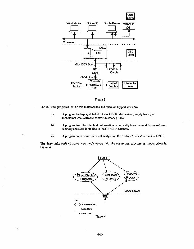
Etbmet---- ---- --- 1-----------
------”’i-’m=------I J
Figure 3
me software programs that do this maintenance and operator support work are
a) A program to display detailed interlmk fault information dirudy from tiemodulators ld software controls memory ~L).
b) A program to coll~t the fault information periodically from the modulators softwarememory and store it off-lke h tie OWC~ database.
c) A program to perform statistical analysis on tie ‘historic’ data stored in OW~E.
me thr= tasks oudind above were implement witi the connection smcture as shown below inFigure 4.
maE
~ “r’ve’---- ---- ---- --- ---- ---- ---- -*
440

Some of the data windows that are created for the direct @by of faulty interlock data are shownbelow in Figure 5. There is rdso stored witiin the program a complete flow chart of the interlock levelfunctioning to add more on-line maintenance and diagnostic information.
Figure 5
Conclusions.
It mms very clear that in any future linear collider using large numbers of Mysmonmodubtors thatreliabtiity, avaibbdity and maintainability must k phced on a par with wall-plug power efficiency ifdowntime is to be minim- The approach ud for tie small, but important L~ Uystron moduhtorsystem, which is part of the lepton production proc~s, has kn to build in smart fault reporting andpro~tion equipment as descni. This has resulti in a reduction of modulator downtime tim 8%to less than 170 for a average ywly running time of 6000 hours. This reduction has been achievdover a period of about four years, during which a steady investment of equipment and software hasbeen made.
To complement tiis development, tests we now Ming made with MCODWS work managementsoftware to provide on-line flow-chart checking procedures for faultfinding, ~uipment =tting-up andcrdibration. In addition, ~View programs have been written that enable standard power calibrationtests to be quic~y made, and the results stored away on computer memory for maintenance rwordingpurposes. Ml of these ar~ of system improvement are contributing to a higher quipment avatiabfityin havingmtiulators that are simply _~ntained ~d Reliably lWtti (s~~.
References.
Ww Grippeling,1993, ‘me Design and Development of a G-64 based Interlock System for LPIModulators”, ~PSH Note 93-01 Owh).
Man Campbefl, 1993, “Fatit Dam Acquisition fiojwt for the LPI Modulators”,Cw~S~P Note 936 Wech).
Ryan Gilmour, 1994, “User Level Software for the New Interlock System of the LPI WystronM~ulators”, ~~SN Note 94-36 ~~h).
441

Implementation of DiagnosticHardware and Software Systems for
CERN Modulators
n/“--“---.’’’\.\,I~\]i-) ~ ;(J i.... ‘ i
,j
I\
i/
‘\,\....,
/’
~..---_..-../’
P.Pearce, G. McMonagle and G. Rentier
CERN, PS Division, Geneva Switzerland
SLAC Modulator-Klystron Workshop 9thto 1lth Octber 1995

4
●
●
●
●
●
Requirements for New InterlockSystem
Memorisation of modulator faults including time and dateof failure with local display panel
High reliability
Intetiacing to control system (and later on to ORACLEdatabase)
Fail-safe with no ambiguous fault indication
Complete input signal and data output compatibility withthe old interlock system
<onforming to CERN personnel security requirements‘-.’‘\ I

Choice of Svstem
n/“’------>’’’1,,iKV,,-\~ ;
(/ 1.... ‘ I y/
‘\.\. /:
....-.. ./.--------

Hardware Details for Full Project Implementation
A!
—— —— ———
ML-1
ML-l=fiMW
\y_...y

.,,
Direct Display Program
n~<”-”“---’.’”’l,[y\] \\/5..T1 ,!
! \i;
‘\.\ /’.....
.,.. ..--------

,L,: :l--;~~~i_--”’,,,,,
I,4, ,,,,, ,, I
“>W L #“- N on
~
+ II---- ---- ---- ---- ---- ---- --
ti --- 11
t0,
--
447

L,#t
L, :
u/#
a“
—1 11,L/ ,
---- - ---- ---- ---- ---- ---- -- - t ) --<- )------’
‘>448

NewInterlocksystemIncludingUser Level
❑UserLevel
Wofistation OfficePC OracleServer ORACLE
A soft and Firmware View of the New Interlock System
EthernetI----- ----- ---- ----- ----- ---
rlDSC.
TBL @.
m----------------------------MlL-l 553 BUS
RTI Other RTI
Card
G-M BUS
Interlo&
n
“..---~~..lfablts/“”” .\,/
Rv!-’~ ,;\/ !.... ! ‘t;I i
J;‘\.\.,, i’.. -/.---------
Cards
---- -
❑DSCLevel
---- -
m
User kvel
*----- ----- ---- ----- ----- ----- --- ----
Lm
h=nMETH
mm-,titi~mabm
?
---- ---- ---- --- ---- ---- ---- -- ----- ----
DC bvel
+ Data flow

Range of User Level Software
muOracle RDatabase
/4~
o
OracleR Display
w stats ProcesR Amlysis
Process
q =~
IarmDirect SystemDisplay ProcessProcess
RN R
/R
FAULT DATA ACQUISITION!!T~~!

Chosen Design Architecture-VME based using the Ml L-l 553-B Field Bus Hardware
R/“-”““---..’\.\I
,.n .~ KV(/ i....‘ Ii ‘Y
I\
/\ /’
“...------------ ~.
MDK 29
Y
-gg~g _,:.:,,.,.,:,.,.,.,,.,...,.
tin
LMDK 27
~ggg =8..:.:.:..,...:,:.:,.,,,,.:.:
%~
MDK 31,.
_~gg~ m:,.,..,.,,,.,,.. .. .... .:,.,..:.
%
1
~

ma
s0
■ -
I
III
452

Protection Response Time of Modulator
18-May-9313:21:48A:M1
[1
20 ms
1.0v
At 66.10ms
1 DC 12.8 V
CH1 (A) represents the interlock that goes from a good status to a bad status.The response time of the output signal is 66. 1E1O-3seconds on average

I 1
.
454

/ 1I
455

R/“””“---.’”’\,l
p’~ ,!~\j
\/ i._. ! ‘j‘\\.,, ;’
-..-__.-..-’
----- .

.. .. .

Implementation of diagnostic Hardware and Software systems for CERNmodulators
P. Pearce, G. McMonagle and G. Rentier .C~N, PS Division, Geneva, Swiherland
1.Introduction
At the PS Klystron - Moduhtor Workshop, October 1991, a suggested improvement for the LLModulator systems was “An interlock memorisation systemiprogram that wdl enable intermittentmodutator faults to be captured and stored over a period of time.” The existing static relay systembasti upon 120 relays, for one modulators interlocks, would not be able to provide this functiotitytiause it is entirely an dogue system with no memory capacity. As a result of tiis, a new interlocksystem was designed in accordance with the following requirements.. Complete input signal and data output compatibility with tie old interlock system● Fail-safe with no ambiguous fault indication● High reliability● Memorisation of modubmr faul~ including time and date of failure with a local display panel● Interfacing to control system (and later on to Oracle database)● Conforming to CERN personnel swurity requirementsA G-a 8 bit micropr=or<ontrolled system was chosen as similar equipment was akeady beingused by the power group to control power supplies. Thus the development and liaison with indus~had alrady been establish and tiere was considerable expertise already available in the PSDivision.me new interlock system was designed and implemental in 3 stages.● G-@ microprocessor intalock system with local memorisation of faults● Fault data acquisition from G-W system via ~ 1553B bus. allowing tie information to be stored
in ORACLE data he and giving access to current information from remote terminals.● User level software for mting data storti in ORACLE data base for creating statistical
information of past faults.At the momenta new ON~~ co-ordinator, which allows local or remote control of the modulator, isbeing develo~ tiso using a G-a microprocessor system, which will be linked to tie new interlocksystem and tie ~-1553B data bus.
2. Original intetlock system and inherent problems
Each original relay intalock system was designed to protect the moduktor hardware from excessivedamage if a fault OCCW Up to 120 input signak, coming from semi-static and ~ time operatiodsub-assemblies within each moduhtor were continuously processed. These input signals operated 120separate d.c. relays in each interlock unit. The output rehy contac~ were organiti into 4 separateinterlock chains, corresponding to the 4 output control levels (Off, Heater, Standby, Pulsing). A d.c.current of about 20mA flowed through every contact in each of the series chains of contacts, enablingtie four output protection conditions.During normal production operation the modulator system works continuously for many months at atime. Throughout this period many intermittent faults occurred, mainly due to contact oxidisationsince tie relays stayed in a activated closed position. This oxidisation build up inc~d the systemdowntime in a random fashion. In addition, because individual interlocks were not memorised thefault finding and separation of true external faul~ from internal contact problems provd difficult.
3. Micro-processor interloek system
To overcome these difficulties a more reliable system has kn designed using commercial solid stateG-M micro-proe~sor and opto coupled interface board Whnology to replace the rehy logic. The newscheme apart from improving modulator reliability stores up to eight complete fault squences in Iml
458

memory, in a fully time ordered presentation. Within each fault squence the fmt eight faultyinterlocks are memorised together with a date and time tag to give maximum fault information.
Hardware desireThe new stand-alone protection system has been develo~ that uses tie MC68W, 8 bit micro-processor witiin a G-a data bus crate as shown in Figurel. This system handles tie 120 inputsignals via purpose designed 32-way input buffer cards. fich input interlock signal generates thefollowtig thr= output signals.1) A high priority direct interlock connection to tie 32-way input card for moduhtor protection2) An opt~isolated output for the existing CAMAC data acquisition3) A ~ level output for on board testing purposa
=60 INTERLOCKS
figure 1 Micro-processor controlled interlock hardware scheme
Four 32 way input cards hande the interlocks in groups of eight and ay one of these groups cangenerate a hardware interrupt for tie procmsor. The faded interlock groups are then collectd by theprogram and stord in a local memory. Any interrupt is processed immediately by an interrupt serviceroutine ~SR), which changes the output status as rquired. The MC68W micro-processor can addressa toti of ~kbytes of memory. The interlock program is stored in ~ROM together with the intemptand start vector addresses. The 16 way output board mnnects the G@ system with tie moduktor viaopto-coupled links and a buffer card. Four output levels react directiy with the modulators powercircuits and control its status. A fifth output level is used as a watchdog and monitors the functioningof the pr-ssor via a status fine that is togglti by the software. If this fine stops toggfing, theprogram has stopped running and the pro~tion system is no longer working and the modulator isimmediately put to the OFF state. The machine access control and N protection doors ako provideinterlock contacts that are direcdy connectti in series with the output level contacts to give addihonrdpersona security.=ROM software developmentThe main interlock program is a loop that includes the acquisition and treatment of the 120 inputsignals and has kn written in Pascrd. me program ‘display’ variable is used to make sure hat thedisplay screen information is written without interruption from any other keyboard action that occursduring this operation. The initialisation, start-up and interrupt routines have been written inassembler micr~ode.Two sourca of system interrupt that can OCCW.One that is generated by afaulty interlock and a second by a key on the units display panel. However the interlock generated
459

interrupts have priority over any display r~uests. The ovedl intemd response time between the
change of input signal and the RQA line on the G-64 bus due to the oto<ouplers is about 14 ps.
When a fault occurs tie interrupt service routine is immediately executed and any sub~uent newinterrupts are disabled whikt the input group that caused the first interrupt-is traced by means of apolling routine. The output status of the prowtion system is switchd to the assigned operating leveland so protecting the modulator. Finally the interrupt flag is clmed and the faulty interlock is storedalong with the date and the time tags.The display scra on ~ch interlock unit allows the fo~owing display modes to be sel~ti:● Mode 1 Checks system memory and is automatically activati when pulsing● Mode 2 Displays current status of interlocks● Mode 3 Changes date and time. Mode 4 Displays information and error messagesfich disphy mode has a software driver module containing special functions and prmdures.
4. The new interlock system implementation.
The new interlocksystem d~ign uses threedifferentlayersof hardware and software. This enabl~the fault data to be available at the three basic system levels which are:1) Stand-alone modulator interlock protection2) Front<nd procmsor @evice Stub Controller) level3) @rational user levelThe system hardware scheme based on these thr= levels is shown in Figure 2
W--———__ __ ____7 F –+– <–A– –
T
/ MIS
Figure 2 System hardware schematic diagram
Interlock protection levelAt tie interlock hardware level each G-M interlock unit has a Remote Terrnind Interface @TI) cardpluggd into i~ data bus. The multi drop ML-1553-B field bus connects this card to the a~eleratorconwols system. This enables the asynchronous exchange of data in response to commands from theBus Controller @C) in the front end processor @SQ. The two buffer memoriw on the RTI cad are
460

used as Rweive and Transmit FfFO buffer stacks tiat hold control values and the G-64 acquisitiondata. A Control and Status Register (CSR) bit (TB) indicates to the BC that the interlock data hasbeen loaded into the Wsmi[ buffer memory. me TB bit is only reset after the transmission iswmplete. A data transmission rate of 1 MbiWs is used.The interlock micro-processor has a set of f~mware assembler instructions tiat are used to load thefaulty interlock data into tie transmit buffer on the R~ card. me DROM program is triggered intoaction by hardware interrupt on the occurrence of the fwst faulty interlock. An intemd delay ensu~the ~pture md storage of up to a maximum of Xven sub~uent cascading interlocks before the R~wsmit buffer is loaded. The worst case acquisition time measured for a complete sequence ofcascading interlocks was 116 ms. However, the measured average protection response time to put themodulator to a non pulsing state, after the fault event occurs, is about 66 ms as shown in Figure 3
at Ulo”
1 ,x #a”Rgure 3 Protection response time of modulator
Front<nd proc~sor levelAt the DSC level a rd time software task has been written in C language and runs under the controlof the Lynx ~ Me) operating system. The R~ buffer cards are scanned every 20 wends by thtitask to check for any new dam A repmentation of the rml time task software rdgorithm is shown inFigure 4. If data is avaihble from the R~ card it is taken, the CSR bit is cleared and tie data isreformatted and stord. The reformatting process consists of removing any padding characters andd=imrd points from the fixd length 32 byte message. me interlock numbers are then converted intomrresponding 32 bit integer values and the U~ system date and time is attached. Finally theposition to store the fault message in the data table ~L) is mlcuhted and the data is stored. Onetable is used for each modulator. These tables are Iwted within the specflc software @uipmentModule @~ drivers u@ for LPI modulator control and acquisition.
~~figure 4 Real-time @k algorithm
461

Operational user levelA dir~t dispby program on the controls network enabl= the operations and maintenance staff to see~uipment faul~ diratiy from a selectd modulator, for a particular date and time. me displayti datais obtained either from the current contents of tie data table ~L), or from the historical data in tieOracle database. me programs interactive disphy is shown in Figure 5. -
A rd time task collwtor program runs daily to extract data from the ~L of ~ch modulator andreformats it before sending it to the Oracle database. A statistical analysis program has been writtenusing Microsoft Acres Q, which enables the data in Oracle to be studied in looking for trends offaults due before component failure. me range of existing and future (AM System Process) usersoftware is shown in Figure 6.
\ \ 4FAULT OATA AC OUISITIOI
-T BL -
figure 6 Range of user level softiare
M
5. Summary
Ml L~ modulators have ~n quipped with the new G-64 interlock system. ~ese have kn fillyintegratd into the accelerator control system, providing detailed fault information for both operatorsand maintenan~ staff. me modu~tor system reliability has been signtlcantiy improvti as a r~ult oftiis developmmc It is ex~ted that the future implementation of the new ON/OFF coordinator units,under development and using the same t~hnology, will further improve the operational fatures andreliabihty of the moduktor system.
6. References
M.Grippeling, ‘me design and development of a G& based interlock system for use with the LPI35 MW pulsed power moddators.”, CERNPSLP Note 9341 ~ech)
A. Campbell, “Fault data acquisition projwt for the LPI modulators”, CERNpS~P Note 93-66
D. Francart et d, “ML-1553-B Multidrop bus for controlling LEP and SPS quipment”,CERN/SPS/ACC Note 85-26 Rev
J. Cuperus, W. Heinm and C.H. Sicard, “me control module handboo~’, CERNRS/CO Note 91-25
R. GIhour, “A ftity interlock display program for LPI modulators”, CERN&S~p Note 94-22
462

SMT MODWATOR SESSION SWARY
J. de hare
The gods in a SMART modtiatormystron design are to ~imize amelerator availabfity andsystem efficiency. These gods are more easfly accomplished when the modulator and Mystrondesigns are integrati as a system. The design issues can be summarized into three parts:
A. Maximiz e system rekbifity and efficiency.B. Minimize system diagnosis and reset time.C. Minimize system repair time.
A. Maximize system retiabfity and efficiency
1. Reduce active components where possible to hcrease reliability.2. Explore tradeoffs between system “smarts” and reliability.3. Maximizing efficiency may increase reliability.4. ~wte fedback to maintain high efficiency.5. Evaluate tradeoffs between rdundancy, initird costs, operation costs, and
downtime costs.6. Evaluate tradeoffs in reliability and efficiency for C-band vs X-band accelerators.7. kterlock system should be fail-safe.
B. Minimize system diagnosis and reset time
1. ~ovide diagnostics for personnel safety, system safety, feedback, and readback.2. System shotid be self resetting for minor fatits to minimize reset time.3. Diagnostics avtiable loc~y and remotely.4. Store fault md operation information in database.5. R=ord fatit information with time, date and squence stamp.6. Use digitizer to sample system waveshapes and record ano~ies.7. Diagnostics must be reliable and inexpensive.8. ~ystron processing after a vacuum fault should be automated.
c.Minimize system repair time
1. Sub-systems should be modular.2. System shotid provide information necessary to ex@te repair.3. Design system for ease of maintenance.
463

AUTHOR INDEX
Akemoto, M. 126Ashton, J. 413, 423
Baba, H. 138
Barnes, M. 258, 320, 339Bees, G. 148Bieler, M. 221Burkes, T. 154
Caryotakis, G. 51, 344Cassel, R. 81Cho, M. H. 138, 389,408Choi, M. 250Choroba, S. 208, 221Creedon, J. 288
DeLamare, J. 463Dinkel, J. 159DoUson, A. R. 1, 2, 423, 426Ducimetiere, L. 293
Eichner, J. 189
Faure, P. 293
FicMin, D. 292, 351
Giebeler, R. 221Gold, S. 71, 166, 189, 221Grippe, J. 228Grunwdd, H. 272, 288Gundersen, M. 250, 312
Harneister, J. 221
Jarnsson, U. 293
Koonti, R. 166, 189,
Lechatellier, R. 229hWti, H.-Ch. 221Uyh, G. 160, 162
MCGOWaU,J. 288McMomgle, G. 374,437, 442,458Matsumoto, H. 138Mtiuno, H. 192
Oh, J. S. 138,408
Park, S. S. 408Pearce, P. 138, 244, 355, 374, 427, 437, 458Pfeffer, H. 164Pirrie, C. A. 341
Rentier, G. 374, 458Riege, H. 293Ruth, R. 5
ScMaug, M. 293Schroder, G. H. 293Sheldrake, R. 341Sheppard, J. 426Shidara, T. 224, 380Shintake, T. 138
Vossenberg, E. B. 293
Wait, G. 258, 320Watanabe, K. 138Weatherup, C. R. 341Wilson, P. 28, 45Wright, E. 72
yampls~, I. 250
Namkung, W. 138, 408Nesterov, V. 319
464


