Embed Size (px)
Citation preview
All-Oxide PhotovoltaicsSven Ruhle,* Assaf Y. Anderson, Hannah-Noa Barad, Benjamin Kupfer, Yaniv Bouhadana,Eli Rosh-Hodesh, and Arie Zaban*
Department of Chemistry, Bar Ilan University, Ramat Gan 52900, Israel
ABSTRACT: Recently, a new field in photovoltaics (PV) has emerged, focusing on solarcells that are entirely based on metal oxide semiconductors. The all-oxide PV approach isvery attractive due to the chemical stability, nontoxicity, and abundance of many metaloxides that potentially allow manufacturing under ambient conditions. Already today,metal oxides (MOs) are widely used as components in PV cells such as transparentconducting front electrodes or electron-transport layers, while only very few MOs havebeen used as light absorbers. In this Perspective, we review recent developments of all-oxide PV systems, which until today were mostly based on Cu2O as an absorber.Furthermore, ferroelectric BiFeO3-based PV systems are discussed, which have recentlyattracted considerable attention. The performance of all-oxide PV cells is discussed interms of general PV principles, and directions for progress are proposed, pointing towardthe development of novel metal oxide semiconductors using combinatorial methods.
The market for photovoltaic (PV) modules has shownnearly exponential growth over the last years, with a peak
power of more than 25 GW installed in 2011, leading to acumulative installed capacity of ∼70 GW.1,2 For comparison, atypical nuclear power plant can produce around 1 GW. Eventhough the PV sector is booming, PV-generated electricity inmost places can still not compete in price with conventionallygenerated electricity and is consequently dependent onsubsidies.3 To reach grid parity, further price reductions forPV systems are required, calling for continued up-scaling of theproduction processes or for novel PV cell concepts based oncheap materials and low-cost deposition methods. Metal oxide(MO) semiconductors are very attractive to achieve that goal;they are chemically stable, and many MOs are nontoxic,abundant, and fulfill the requirements for low-cost manufactur-ing methods at ambient conditions. Consequently, devicesmade of MO semiconductors can be very inexpensive, stable,and environmentally safe, which are, besides the conversionefficiency, the most important requirements for PVs. From theoptical point of view, there are a number of MOs suitable forPV applications. However, the electronic properties of mostknown MOs, that is, the short lifetime of excited electronicstates and low mobility of electronic charge carriers, preventedtheir use as active solar cell materials. Here, we give aperspective on all-oxide PVs as a future technology foreconomic energy generation. We show where MOs are todayapplied as components in PV cells, review existing all-oxide PVsystems, and discuss their limitations. Combinatorial methodsare proposed for synthesis of novel multicomponent MOs,including doped oxides, new crystalline or amorphous MOs,and MO composites, which can overcome the currentlimitations.Metal Oxides in PVs. MOs are today widely used as
components in PV cells and modules, mainly as transparentconducting oxides (TCOs).4,5 Fluorine-doped tin oxide (FTO),
indium tin oxide (ITO), or aluminum-doped zinc oxide (AZO)are the most common TCOs and widely applied incommercially available thin film solar cells based on CdTe,CuInxGa1−xSe2 (CIGS), and amorphous or microcrystalline Si,which have a market share altogether of around 17%.1 BesidesPV, TCOs are used in consumer electronics for flat paneldisplays, touch screens, and smart phones. Very dynamicresearch is reported from the field of thin film transistors basedon wide-band-gap MOs, which are very attractive due to theoptical transparency that is added to the electronic function-ality.6
Promising next-generation nanocomposite PV cells such asdye-sensitized solar cells (DSCs),7 quantum-dot-sensitizedsolar cells (QDSCs),8 or extreme thin absorber cells (ETAcells)9 are based on nanostructured MO electrodes that aredeposited onto a TCO substrate and are coated with a thinabsorber layer from which charge carriers (in most cases,electrons) are injected into the MO upon photoexcitation.10,11
Nanostructured electrodes based on TiO2,12 ZnO,13 SnO2,
14
SrTiO3,15 Nb2O5,
16 and ZrO217 have been used as wide-band-
gap electron conductors, while NiO has been used as a hole-transport material.18 Light to electric power conversionefficiencies of 11−12% have been achieved with DSCs where
Received: October 22, 2012Accepted: November 30, 2012Published: December 5, 2012
Recently, a new field in photo-voltaics has emerged, focusing onsolar cells that are entirely basedon metal oxide semiconductors.
Perspective
pubs.acs.org/JPCL
© 2012 American Chemical Society 3755 dx.doi.org/10.1021/jz3017039 | J. Phys. Chem. Lett. 2012, 3, 3755−3764
a mesoporous TiO2 film was used as an electron conductorwith a high microscopic surface area for dye adsorption.19,20
Recently, mesoporous Al2O3 was used as a high-surface-areamatrix to accommodate an organometallic halide perovskiteabsorber and spiro-OMeTAD as a hole conductor. In contrastto the common DSC, QDSC, or ETA cell concepts, no chargeswere injected into the mesoporous Al2O3, leading to solar cellswith an efficiency above 10% due to efficient electron transportalong the absorber coating.21 MO electrodes can be producedin a variety of nanostructures such as mesoporous films,22
nanorods,23 nanowires,24 nanotubes,25 and more complexmorphologies,26,27 with ZnO being the most versatile materialin terms of growth conditions and shapes.28 For polymer-basedPV cells, MOs such as TiO2 and ZnO have been used aselectron acceptors in flat29 as well as nanostructureddevices.30−32 As hole-transport materials, NiO,33 V2O5,
34
WO3,35 and MoO3
36 have been used in organic solar cells.37,38
Cu2O-Based All-Oxide PVs. In this Perspective, we present acomprehensive view of all-oxide PV, from which one can gainbetter understanding of the system and point out directions forprogress. Only a few MOs have been investigated as lightabsorbers for PV applications where Cu2O is the most popularmaterial (see Table 1), with extensive research going back to
the 1970s.64,65 As a single-junction device, its electronic bandgap of approximately 2.0 eV is not ideal for the sun spectrum(AM1.5G), leading to a maximum theoretical conversionefficiency of ∼23% compared to 32.9% for an optimizedband gap of 1.34 eV (detailed balance limit).66 However, as atop cell in a multijunction stack consisting of three or morejunctions, its band gap is nearly optimized;67 furthermore,Cu2O can be a very attractive absorber for semitransparent PVcells.Cu2O can be produced by a number of methods, including
high- and low-temperature thermal oxidation,68 electrochemicaldeposition,69 anodic oxidation,70 spray pyrolysis,71 and reactivesputtering72, and is mostly p-type. Initial PV device structureswere based on a Schottky junction, where it was found that the
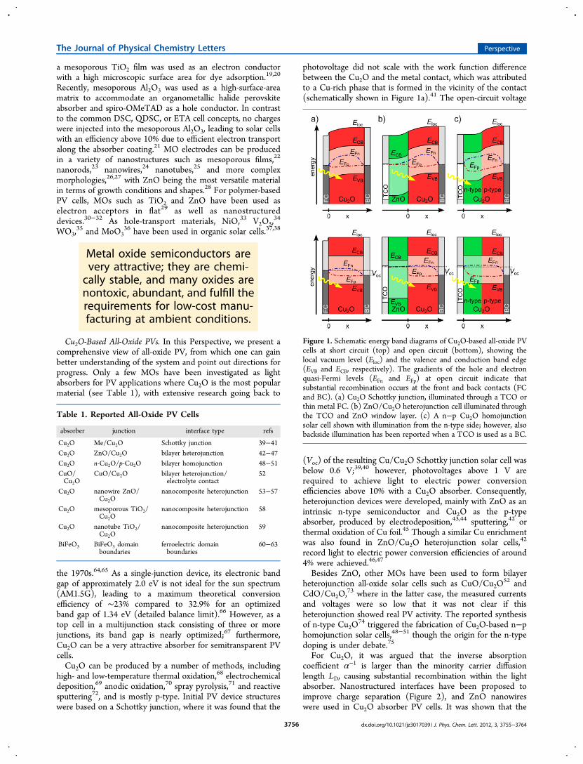
photovoltage did not scale with the work function differencebetween the Cu2O and the metal contact, which was attributedto a Cu-rich phase that is formed in the vicinity of the contact(schematically shown in Figure 1a).41 The open-circuit voltage
(Voc) of the resulting Cu/Cu2O Schottky junction solar cell wasbelow 0.6 V;39,40 however, photovoltages above 1 V arerequired to achieve light to electric power conversionefficiencies above 10% with a Cu2O absorber. Consequently,heterojunction devices were developed, mainly with ZnO as anintrinsic n-type semiconductor and Cu2O as the p-typeabsorber, produced by electrodeposition,43,44 sputtering,42 orthermal oxidation of Cu foil.45 Though a similar Cu enrichmentwas also found in ZnO/Cu2O heterojunction solar cells,42
record light to electric power conversion efficiencies of around4% were achieved.46,47
Besides ZnO, other MOs have been used to form bilayerheterojunction all-oxide solar cells such as CuO/Cu2O
52 andCdO/Cu2O,
73 where in the latter case, the measured currentsand voltages were so low that it was not clear if thisheterojunction showed real PV activity. The reported synthesisof n-type Cu2O
74 triggered the fabrication of Cu2O-based n−phomojunction solar cells,48−51 though the origin for the n-typedoping is under debate.75
For Cu2O, it was argued that the inverse absorptioncoefficient α−1 is larger than the minority carrier diffusionlength LD, causing substantial recombination within the lightabsorber. Nanostructured interfaces have been proposed toimprove charge separation (Figure 2), and ZnO nanowireswere used in Cu2O absorber PV cells. It was shown that the
Metal oxide semiconductors arevery attractive; they are chemi-cally stable, and many oxides arenontoxic, abundant, and fulfill therequirements for low-cost manu-facturing at ambient conditions.
Table 1. Reported All-Oxide PV Cells
absorber junction interface type refs
Cu2O Me/Cu2O Schottky junction 39−41Cu2O ZnO/Cu2O bilayer heterojunction 42−47Cu2O n-Cu2O/p-Cu2O bilayer homojunction 48−51CuO/Cu2O
CuO/Cu2O bilayer heterojunction/electrolyte contact
52
Cu2O nanowire ZnO/Cu2O
nanocomposite heterojunction 53−57
Cu2O mesoporous TiO2/Cu2O
nanocomposite heterojunction 58
Cu2O nanotube TiO2/Cu2O
nanocomposite heterojunction 59
BiFeO3 BiFeO3 domainboundaries
ferroelectric domainboundaries
60−63
Figure 1. Schematic energy band diagrams of Cu2O-based all-oxide PVcells at short circuit (top) and open circuit (bottom), showing thelocal vacuum level (Eloc) and the valence and conduction band edge(EVB and ECB, respectively). The gradients of the hole and electronquasi-Fermi levels (EFn and EFp) at open circuit indicate thatsubstantial recombination occurs at the front and back contacts (FCand BC). (a) Cu2O Schottky junction, illuminated through a TCO orthin metal FC. (b) ZnO/Cu2O heterojunction cell illuminated throughthe TCO and ZnO window layer. (c) A n−p Cu2O homojunctionsolar cell shown with illumination from the n-type side; however, alsobackside illumination has been reported when a TCO is used as a BC.
The Journal of Physical Chemistry Letters Perspective
dx.doi.org/10.1021/jz3017039 | J. Phys. Chem. Lett. 2012, 3, 3755−37643756
short-circuit current density (Jsc) was increased compared tothat for a flat bilayer reference solar cell,54 but the conversionefficiency remained below 1%,53,55−57 thus significantly belowthe performance of the good bilayer systems. Furthermore,Cu2O was grown electrochemically within mesoporous TiO2films58 and arrays of TiO2 nanotubes,59 but also here, theconversion efficiency remained below 1%.BiFeO3-Based PVs. PV cells based on ferroelectric oxides such
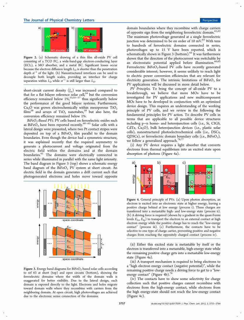
as BiFeO3 have been reported recently.60−63 Solar cells with alateral design were presented, where two Pt contact stripes weredeposited on top of a BiFeO3 film parallel to the domainboundaries. Even though the device had a symmetric structure,it was explained recently that the required asymmetry togenerate a photocurrent and voltage originated from theelectric field within the domains and at the domainboundaries.61 The domains were electrically connected inseries while illuminated in parallel with the same light intensity.The band diagram in Figure 3 (top) shows a schematic energyband diagram of the BiFeO3 PV system at short circuit. Anelectric field in the domain generates a drift current such thatphotogenerated electrons and holes move toward opposite
domain boundaries where they recombine with charge carriersof opposite sign from the neighboring ferroelectric domain.61,63
The maximum photovoltage generated at a single ferroelectricjunction was determined to be on order of 10 mV.63 With tensto hundreds of ferroelectric domains connected in series,photovoltages up to 15 V have been reported, which isschematically shown in Figure 3 (bottom).63 It was furthermoreshown that the direction of the photocurrent was switchable byan electrostatic potential applied before illumination.60,62
Ferroelectric BiFeO3-based PV cells have recently generatedconsiderable interest; however, it seems unlikely to reach lightto electric power conversion efficiencies that are relevant forelectricity generation. The intrinsic limitations of BiFeO3 forPV applications will be discussed in more detail below.PV Principles. To bring the concept of all-oxide PV to a
breakthrough, we believe that more MOs have to beinvestigated for PV applications and new multicomponentMOs have to be developed in conjunction with an optimizeddevice design. This requires an understanding of the workingprinciple of PV cells, and we review in the following thefundamental principles for PV action. To describe PV cells interms that are applicable to all possible device structuresincluding p−n homo- and heterojunction cells (i.e., Si, CIGS,CdTe, Cu2O), bulk heterojunction devices (i.e., plastic solarcells), nanostructured photoelectrochemical cells (i.e., DSCs,QDSCs), or ferroelectric domain boundary cells (i.e., BiFeO3),we follow a generalized approach.76,77
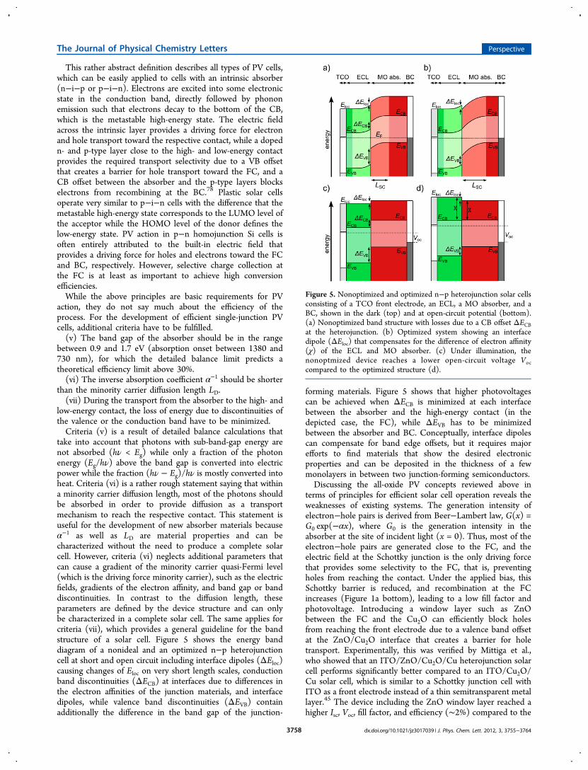
(i) Any PV device requires a light absorber that convertselectrons from thermal equilibrium into an excited state uponabsorption of photons (Figure 4a).
(ii) Either this excited state is metastable by itself or theelectron is transferred into a metastable, high-energy state whilethe remaining positive charge gets into a metastable low-energystate (Figure 4a).(iii) A transport mechanism is required to bring electrons to
a “high electron energy contact (negative potential)”, while theremaining positive charge needs a driving force to get to a “low-energy contact” (Figure 4b).76
(iv) The contacts have to show some selectivity for chargecollection such that positive charges cannot recombine withelectrons from the high-energy contact, while electrons fromthe high energy-state should not reach the low-energy contact(Figure 4c).
Figure 2. (a) Schematic drawing of a thin film all-oxide PV cellconsisting of a TCO FC, a wide-band-gap electron-conducting layer(ECL), a MO absorber, and a metal BC. Significant losses occurbecause the electron diffusion length LD is shorter than the penetrationdepth α−1 of the light. (b) Nanostructured interfaces can be used todecouple both length scales, providing an interface for chargeseparation within LD while α−1 is still larger than LD.
Figure 3. Energy band diagrams for BiFeO3-based solar cells accordingto ref 63 at short (top) and open circuits (bottom), showing theferroelectric domains where the width of the domain walls isexaggerated for better visibility. Due to the lateral design, eachdomain is exposed directly to the light. Electrons and holes migratetoward domain walls where they recombine with carriers from theneighboring domain. At open circuit, high photovoltages are achieveddue to the electronic series connection of the domains.
Figure 4. General principle of PVs. (a) Upon photon absorption, anelectron is excited into an electronic state at higher energy, leaving apositive charge behind at low energy (process i). These charges aretransferred into a metastable high- and low-energy state (process ii).(b) A driving force is required (shown by a gradient in the quasi-Fermilevels EFn, EFp) to transport the electron to an external contact at highelectron energy while the positive charge has to reach the “low-energycontact” (process iii). (c) Furthermore, the contacts have to beselective to one type of charge carrier, preventing positive and negativecharges from reaching the oppositely charged contact (process iv).
The Journal of Physical Chemistry Letters Perspective
dx.doi.org/10.1021/jz3017039 | J. Phys. Chem. Lett. 2012, 3, 3755−37643757
This rather abstract definition describes all types of PV cells,which can be easily applied to cells with an intrinsic absorber(n−i−p or p−i−n). Electrons are excited into some electronicstate in the conduction band, directly followed by phononemission such that electrons decay to the bottom of the CB,which is the metastable high-energy state. The electric fieldacross the intrinsic layer provides a driving force for electronand hole transport toward the respective contact, while a dopedn- and p-type layer close to the high- and low-energy contactprovides the required transport selectivity due to a VB offsetthat creates a barrier for hole transport toward the FC, and aCB offset between the absorber and the p-type layers blockselectrons from recombining at the BC.78 Plastic solar cellsoperate very similar to p−i−n cells with the difference that themetastable high-energy state corresponds to the LUMO level ofthe acceptor while the HOMO level of the donor defines thelow-energy state. PV action in p−n homojunction Si cells isoften entirely attributed to the built-in electric field thatprovides a driving force for holes and electrons toward the FCand BC, respectively. However, selective charge collection atthe FC is at least as important to achieve high conversionefficiencies.While the above principles are basic requirements for PV
action, they do not say much about the efficiency of theprocess. For the development of efficient single-junction PVcells, additional criteria have to be fulfilled.(v) The band gap of the absorber should be in the range
between 0.9 and 1.7 eV (absorption onset between 1380 and730 nm), for which the detailed balance limit predicts atheoretical efficiency limit above 30%.(vi) The inverse absorption coefficient α−1 should be shorter
than the minority carrier diffusion length LD.(vii) During the transport from the absorber to the high- and
low-energy contact, the loss of energy due to discontinuities ofthe valence or the conduction band have to be minimized.Criteria (v) is a result of detailed balance calculations that
take into account that photons with sub-band-gap energy arenot absorbed (hν < Eg) while only a fraction of the photonenergy (Eg/hν) above the band gap is converted into electricpower while the fraction (hν − Eg)/hν is mostly converted intoheat. Criteria (vi) is a rather rough statement saying that withina minority carrier diffusion length, most of the photons shouldbe absorbed in order to provide diffusion as a transportmechanism to reach the respective contact. This statement isuseful for the development of new absorber materials becauseα−1 as well as LD are material properties and can becharacterized without the need to produce a complete solarcell. However, criteria (vi) neglects additional parameters thatcan cause a gradient of the minority carrier quasi-Fermi level(which is the driving force minority carrier), such as the electricfields, gradients of the electron affinity, and band gap or banddiscontinuities. In contrast to the diffusion length, theseparameters are defined by the device structure and can onlybe characterized in a complete solar cell. The same applies forcriteria (vii), which provides a general guideline for the bandstructure of a solar cell. Figure 5 shows the energy banddiagram of a nonideal and an optimized n−p heterojunctioncell at short and open circuit including interface dipoles (ΔEloc)causing changes of Eloc on very short length scales, conductionband discontinuities (ΔECB) at interfaces due to differences inthe electron affinities of the junction materials, and interfacedipoles, while valence band discontinuities (ΔEVB) containadditionally the difference in the band gap of the junction-
forming materials. Figure 5 shows that higher photovoltagescan be achieved when ΔECB is minimized at each interfacebetween the absorber and the high-energy contact (in thedepicted case, the FC), while ΔEVB has to be minimizedbetween the absorber and BC. Conceptually, interface dipolescan compensate for band edge offsets, but it requires majorefforts to find materials that show the desired electronicproperties and can be deposited in the thickness of a fewmonolayers in between two junction-forming semiconductors.Discussing the all-oxide PV concepts reviewed above in
terms of principles for efficient solar cell operation reveals theweaknesses of existing systems. The generation intensity ofelectron−hole pairs is derived from Beer−Lambert law, G(x) =G0 exp(−αx), where G0 is the generation intensity in theabsorber at the site of incident light (x = 0). Thus, most of theelectron−hole pairs are generated close to the FC, and theelectric field at the Schottky junction is the only driving forcethat provides some selectivity to the FC, that is, preventingholes from reaching the contact. Under the applied bias, thisSchottky barrier is reduced, and recombination at the FCincreases (Figure 1a bottom), leading to a low fill factor andphotovoltage. Introducing a window layer such as ZnObetween the FC and the Cu2O can efficiently block holesfrom reaching the front electrode due to a valence band offsetat the ZnO/Cu2O interface that creates a barrier for holetransport. Experimentally, this was verified by Mittiga et al.,who showed that an ITO/ZnO/Cu2O/Cu heterojunction solarcell performs significantly better compared to an ITO/Cu2O/Cu solar cell, which is similar to a Schottky junction cell withITO as a front electrode instead of a thin semitransparent metallayer.45 The device including the ZnO window layer reached ahigher Isc, Voc, fill factor, and efficiency (∼2%) compared to the
Figure 5. Nonoptimized and optimized n−p heterojunction solar cellsconsisting of a TCO front electrode, an ECL, a MO absorber, and aBC, shown in the dark (top) and at open-circuit potential (bottom).(a) Nonoptimized band structure with losses due to a CB offset ΔECBat the heterojunction. (b) Optimized system showing an interfacedipole (ΔEloc) that compensates for the difference of electron affinity(χ) of the ECL and MO absorber. (c) Under illumination, thenonoptmized device reaches a lower open-circuit voltage Voccompared to the optimized structure (d).
The Journal of Physical Chemistry Letters Perspective
dx.doi.org/10.1021/jz3017039 | J. Phys. Chem. Lett. 2012, 3, 3755−37643758
Schottky-type device. The highest conversion efficiencies ofaround 4% reported today are all based on devices that employan intrinsic n-type ZnO window layer between the TCO andthe Cu2O using AZO as a TCO. This might lead to animproved band diagram with lower energy losses whenphotoexcited electrons are transported from the Cu2O CB tothe FC.46,47 Furthermore, thermal oxidation of pure Cu sheets(≥99.9%) is commonly used to achieve polycrystalline Cu2Owith large single-crystalline grains on the order of tens of mm2,thus reducing recombination at grain boundaries and impuritystates, which finally leads to such promising conversionefficiencies.Cu2O n−p homojunction cells as proposed by McShane et
al.49 or Wei et al.51 were produced without a window layerbetween the TCO and the Cu2O, thus providing arecombination path via the FC, next to the place of thehighest-generation intensity of electron−hole pairs. The Vocand fill factor remained very low (on the order of 100 mV and25%, respectively) when such cells were illuminated from theside of the n-type Cu2O that was deposited onto commercialFTO,51 while better a Voc, Isc, and fill factor were achieved whenthe n-type Cu2O was illuminated via an ITO BC that wasdeposited by sputtering.49 This example shows that the choiceof TCO and deposition method strongly affects the interfaceproperties and subsequently the cell performance. Deuermeieret al., for example, showed that the VB offset at ITO/Cu2Ointerfaces, where both materials were prepared by reactivemagnetron sputtering, can differ by up to 0.5 eV depending onthe deposition conditions such as sample heating.72
In BiFeO3 PV cells, electrons and holes are separated by theferroelectric field in a single domain, which provides someselectivity of charge collection at the contact or, better, at thedomain wall. An intrinsic limitation of BiFeO3 for PVapplication is its rather wide band gap of ∼2.7 eV inconjunction with the low photovoltage generated at aferroelectric domain boundary. If a photon with an energy of2.7 eV excites an electron−hole pair that can generate aphotovoltage on the order of tens of mV, say, for example, 27mV, then 99% of the photon energy is not converted intoelectric energy even if the quantum efficiency for such a processis 100%. Considering furthermore that most of the photonsfrom the sun have an energy below the band gap of 2.7 eV, itbecomes clear that BiFeO3 cells in their current form will notplay a role for energy generation, even though they are a highlyinteresting system from a scientific point of view.New All-Oxide Heterojunction PV Cells. To bring all-oxide PV
to a breakthrough, we believe that new materials have to beinvestigated. We have recently developed new all-oxide bilayerheterojunction cells using CuO and Co3O4 as light absorbers,which have a more suitable band gap for the sun spectrumcompared to Cu2O in order to achieve high light to electricpower conversion efficiencies. Furthermore, we investigatedFe2O3 as a light absorber, which is attractive due to itsabundance and chemical stability. The CuO- and Co3O4-basedPV cells consisted of a FTO FC onto which a compact TiO2layer was deposited by spray pyrolysis,79 followed by pulsedlaser deposition (PLD) of the CuO or Co3O4 absorber. For theBC, a 10 nm thin Cr layer was sputtered to achieve goodadhesion to the absorber followed by a 80 nm thick Au layer toguarantee good electric contact to the external measurementcircuit.I−V curves measured in the dark and under illumination
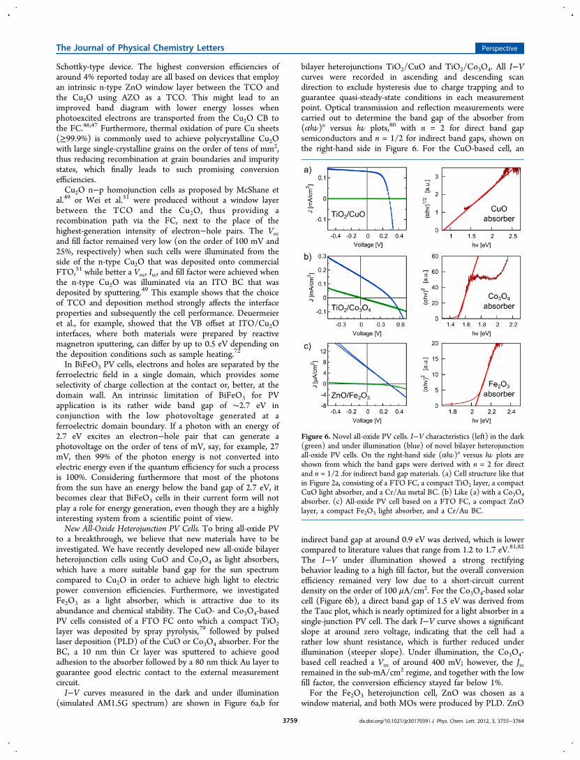
(simulated AM1.5G spectrum) are shown in Figure 6a,b for
bilayer heterojunctions TiO2/CuO and TiO2/Co3O4. All I−Vcurves were recorded in ascending and descending scandirection to exclude hysteresis due to charge trapping and toguarantee quasi-steady-state conditions in each measurementpoint. Optical transmission and reflection measurements werecarried out to determine the band gap of the absorber from(αhν)n versus hν plots,80 with n = 2 for direct band gapsemiconductors and n = 1/2 for indirect band gaps, shown onthe right-hand side in Figure 6. For the CuO-based cell, an
indirect band gap at around 0.9 eV was derived, which is lowercompared to literature values that range from 1.2 to 1.7 eV.81,82
The I−V under illumination showed a strong rectifyingbehavior leading to a high fill factor, but the overall conversionefficiency remained very low due to a short-circuit currentdensity on the order of 100 μA/cm2. For the Co3O4-based solarcell (Figure 6b), a direct band gap of 1.5 eV was derived fromthe Tauc plot, which is nearly optimized for a light absorber in asingle-junction PV cell. The dark I−V curve shows a significantslope at around zero voltage, indicating that the cell had arather low shunt resistance, which is further reduced underillumination (steeper slope). Under illumination, the Co3O4-based cell reached a Voc of around 400 mV; however, the Jscremained in the sub-mA/cm2 regime, and together with the lowfill factor, the conversion efficiency stayed far below 1%.For the Fe2O3 heterojunction cell, ZnO was chosen as a
window material, and both MOs were produced by PLD. ZnO
Figure 6. Novel all-oxide PV cells. I−V characteristics (left) in the dark(green) and under illumination (blue) of novel bilayer heterojunctionall-oxide PV cells. On the right-hand side (αhν)n versus hν plots areshown from which the band gaps were derived with n = 2 for directand n = 1/2 .for indirect band gap materials. (a) Cell structure like thatin Figure 2a, consisting of a FTO FC, a compact TiO2 layer, a compactCuO light absorber, and a Cr/Au metal BC. (b) Like (a) with a Co3O4absorber. (c) All-oxide PV cell based on a FTO FC, a compact ZnOlayer, a compact Fe2O3 light absorber, and a Cr/Au BC.
The Journal of Physical Chemistry Letters Perspective
dx.doi.org/10.1021/jz3017039 | J. Phys. Chem. Lett. 2012, 3, 3755−37643759
has a lower CB edge (further away from the local vacuum levelEloc) compared to TiO2, which is essential to enable electroninjection from Fe2O3. From the Tauc plot (Figure 6c), anabsorption onset at 2.05 eV was derived where, in contrast toliterature, Fe2O3 was treated as a direct band gap semi-conductor because it was not possible to identify a linear regionwhen (αhν)1/2 was plotted versus hν. Further optical andstructural investigations are underway to clarify the origin ofthis behavior. I−V measurements clearly showed PV activity,but the photocurrent remained very low, on the order of a fewμA/cm2. The dark I−V curves of all three all-oxide bilayerheterojunction cells did not show any pronounced rectifyingbehavior in this potential range, while the light I−V curvesdisplay rectification for the CuO- and Co3O4-based cells.Furthermore, all three all-oxide PV systems show a crossover ofthe light with the dark I−V curve, indicating that photo-conductivity plays a role in device operation. The results abovedemonstrate that it is not difficult to find new all-oxide PVheterojunctions with a very low performance. Even formaterials with a nearly optimized band gap such as CuO orCo3O4, the current densities remained roughly 2 orders ofmagnitude below their theoretical limit, calling for bettermaterials and an improved device design.To develop efficient all-oxide PV cells, a combinatorial
approach is proposed where a large number of experiments areconducted on a single substrate. This provides a method for fastdevelopment of novel materials and optimization of devicestructures. We distinguish between (a) combinatorial all-oxidePV cells (device libraries) and (b) combinatorial materialscience (material libraries).
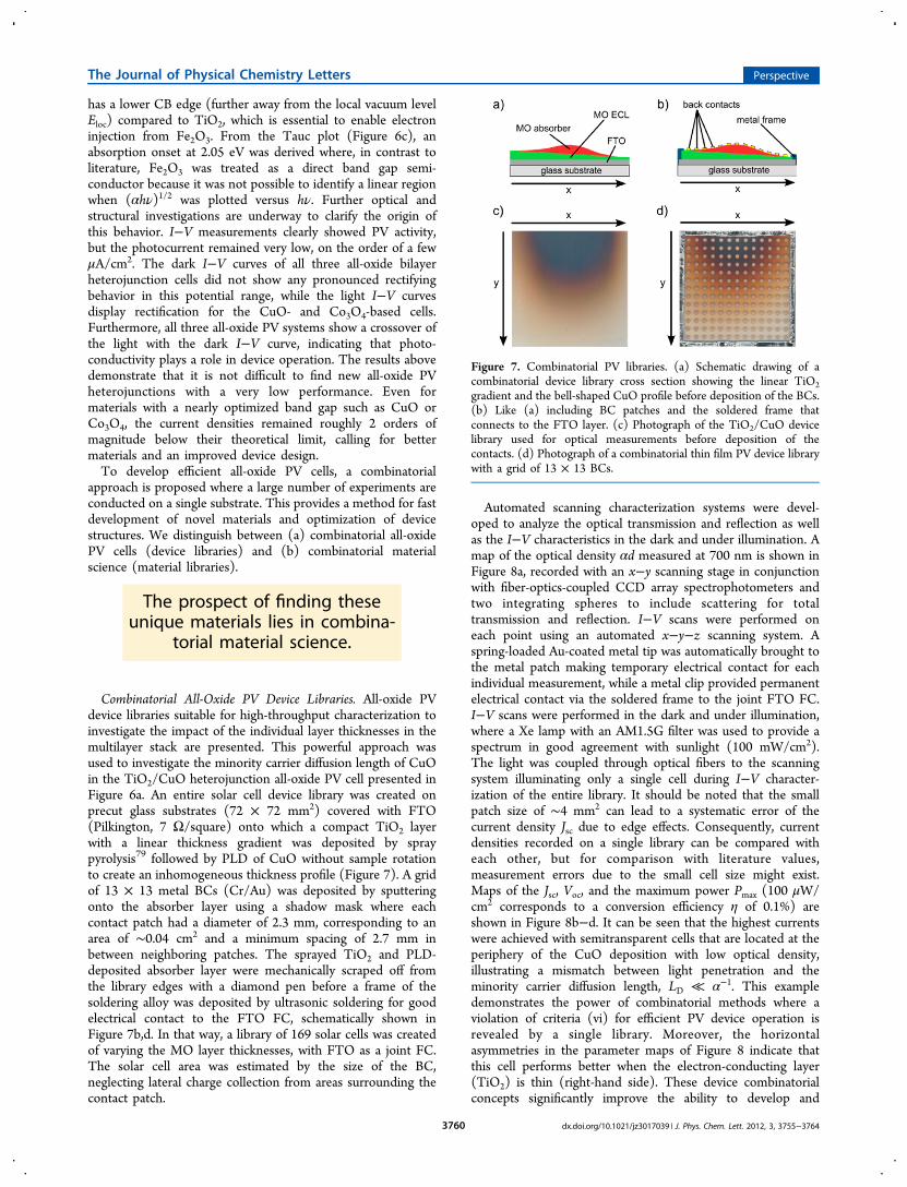
Combinatorial All-Oxide PV Device Libraries. All-oxide PVdevice libraries suitable for high-throughput characterization toinvestigate the impact of the individual layer thicknesses in themultilayer stack are presented. This powerful approach wasused to investigate the minority carrier diffusion length of CuOin the TiO2/CuO heterojunction all-oxide PV cell presented inFigure 6a. An entire solar cell device library was created onprecut glass substrates (72 × 72 mm2) covered with FTO(Pilkington, 7 Ω/square) onto which a compact TiO2 layerwith a linear thickness gradient was deposited by spraypyrolysis79 followed by PLD of CuO without sample rotationto create an inhomogeneous thickness profile (Figure 7). A gridof 13 × 13 metal BCs (Cr/Au) was deposited by sputteringonto the absorber layer using a shadow mask where eachcontact patch had a diameter of 2.3 mm, corresponding to anarea of ∼0.04 cm2 and a minimum spacing of 2.7 mm inbetween neighboring patches. The sprayed TiO2 and PLD-deposited absorber layer were mechanically scraped off fromthe library edges with a diamond pen before a frame of thesoldering alloy was deposited by ultrasonic soldering for goodelectrical contact to the FTO FC, schematically shown inFigure 7b,d. In that way, a library of 169 solar cells was createdof varying the MO layer thicknesses, with FTO as a joint FC.The solar cell area was estimated by the size of the BC,neglecting lateral charge collection from areas surrounding thecontact patch.
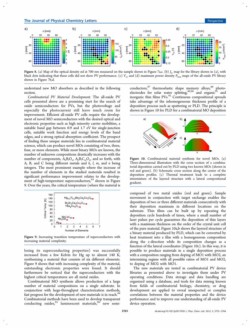
Automated scanning characterization systems were devel-oped to analyze the optical transmission and reflection as wellas the I−V characteristics in the dark and under illumination. Amap of the optical density αd measured at 700 nm is shown inFigure 8a, recorded with an x−y scanning stage in conjunctionwith fiber-optics-coupled CCD array spectrophotometers andtwo integrating spheres to include scattering for totaltransmission and reflection. I−V scans were performed oneach point using an automated x−y−z scanning system. Aspring-loaded Au-coated metal tip was automatically brought tothe metal patch making temporary electrical contact for eachindividual measurement, while a metal clip provided permanentelectrical contact via the soldered frame to the joint FTO FC.I−V scans were performed in the dark and under illumination,where a Xe lamp with an AM1.5G filter was used to provide aspectrum in good agreement with sunlight (100 mW/cm2).The light was coupled through optical fibers to the scanningsystem illuminating only a single cell during I−V character-ization of the entire library. It should be noted that the smallpatch size of ∼4 mm2 can lead to a systematic error of thecurrent density Jsc due to edge effects. Consequently, currentdensities recorded on a single library can be compared witheach other, but for comparison with literature values,measurement errors due to the small cell size might exist.Maps of the Jsc, Voc, and the maximum power Pmax (100 μW/cm2 corresponds to a conversion efficiency η of 0.1%) areshown in Figure 8b−d. It can be seen that the highest currentswere achieved with semitransparent cells that are located at theperiphery of the CuO deposition with low optical density,illustrating a mismatch between light penetration and theminority carrier diffusion length, LD ≪ α−1. This exampledemonstrates the power of combinatorial methods where aviolation of criteria (vi) for efficient PV device operation isrevealed by a single library. Moreover, the horizontalasymmetries in the parameter maps of Figure 8 indicate thatthis cell performs better when the electron-conducting layer(TiO2) is thin (right-hand side). These device combinatorialconcepts significantly improve the ability to develop and
The prospect of finding theseunique materials lies in combina-
torial material science.
Figure 7. Combinatorial PV libraries. (a) Schematic drawing of acombinatorial device library cross section showing the linear TiO2gradient and the bell-shaped CuO profile before deposition of the BCs.(b) Like (a) including BC patches and the soldered frame thatconnects to the FTO layer. (c) Photograph of the TiO2/CuO devicelibrary used for optical measurements before deposition of thecontacts. (d) Photograph of a combinatorial thin film PV device librarywith a grid of 13 × 13 BCs.
The Journal of Physical Chemistry Letters Perspective
dx.doi.org/10.1021/jz3017039 | J. Phys. Chem. Lett. 2012, 3, 3755−37643760
understand new MO absorbers as described in the followingsection.Combinatorial PV Material Development. The all-oxide PV
cells presented above are a promising start for the search ofoxide semiconductors for PVs, but the photovoltage andespecially the photocurrent still leave much room forimprovement. Efficient all-oxide PV cells require the develop-ment of novel MO semiconductors with the desired optical andelectronic properties such as high minority carrier mobilities, asuitable band gap between 0.9 and 1.7 eV for single-junctioncells, suitable work function and energy levels of the bandedges, and a strong optical absorption coefficient. The prospectof finding these unique materials lies in combinatorial materialscience, which can produce novel MOs consisting of two, three,four, or more elements. While most binary MOs are known, thenumber of unknown compositions drastically increases with thenumber of components, AkBlOn, AkBlCmOn, and so forth, withA, B, and C being different metals and k, l, m, and n beingintegers. The most prominent example where the increase ofthe number of elements in the studied materials resulted insignificant performance improvement relates to the develop-ment of high-temperature superconductors,83 shown in Figure9. Over the years, the critical temperature (where the material is
losing its superconducting properties) was successfullyincreased from a few Kelvin for Hg up to almost 140 K,synthesizing a material that consists of six different elements.Figure 9 shows that with increasing complexity of the material,outstanding electronic properties were found. It shouldfurthermore be noticed that the superconductors with thehighest critical temperatures are all metal oxides.Combinatorial MO synthesis allows production of a large
number of material compositions on a single substrate. Inconjunction with large-throughput characterization methods,fast progress for the development of new materials is in reach.84
Combinatorial methods have been used to develop transparentconducting oxides,85 luminescent materials,86 new semi-
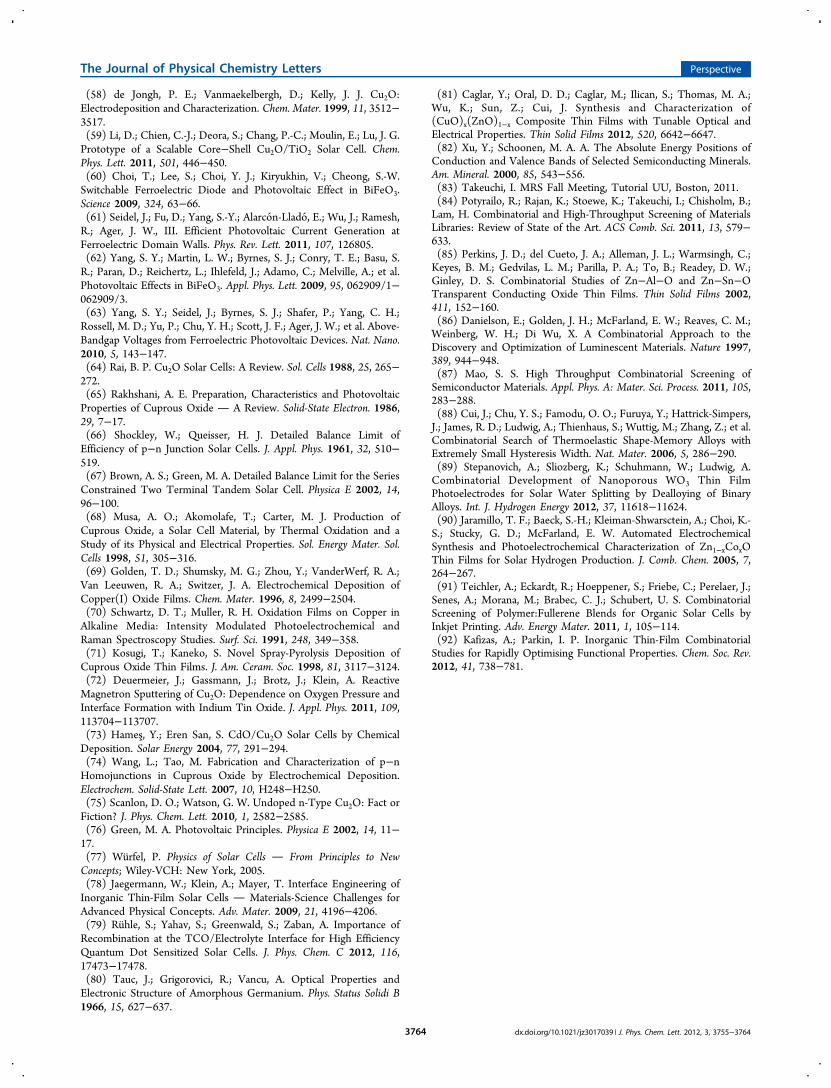
conductors,87 thermoelastic shape memory alloys,88 photo-electrodes for solar water splitting,89,90 and organic91 andinorganic thin films PVs.92 Continuous compositional spreadstake advantage of the inhomogeneous thickness profile of adeposition process such as sputtering or PLD. The principle isshown in Figure 10 for PLD for a combinatorial MO deposition
composed of two metal oxides (red and green). Samplemovement in conjunction with target exchange enables thedeposition of two or three different materials consecutively withtheir deposition maximum in different locations on thesubstrate. Thin films can be built up by repeating thedeposition cycle hundreds of times, where a small number oflaser pulses per cycle guarantees the deposition of thin layerswith a maximum thickness on the order of the crystal unit cellof the pure material. Figure 10a,b shows the layered structure ofa binary material produced by PLD, which can be converted byheat treatment into a film with a homogeneous compositionalong the z-direction while its composition changes as afunction of the lateral coordinates (Figure 10c). In this way, it ispossible to produce materials in a single deposition processwith a composition ranging from doping of MO1 with MO2, anintermixing regime with all possible ratios of MO1 and MO2,to doping of MO2 with MO1.The new materials are tested in combinatorial PV device
libraries as presented above to investigate them under PVoperating conditions. Data storage and data handling areorganized using a database, and tools for data mining knownfrom fields of combinatorial biology, chemistry, or drugdevelopment are applied to reveal unexpected or complexcorrelations between the material properties and the deviceperformance and to improve our understanding of all-oxide PVdevice operation.
Figure 8. (a) Map of the optical density αd at 700 nm measured on the sample shown in Figure 7a,c. (b) Jsc map for the library shown in (a), withblack dots indicating that these cells did not show PV performance. (c) Voc and (d) maximum power density Pmax maps of the all-oxide PV libraryshown in Figure 7b,d.
Figure 9. Increasing transition temperature of superconductors withincreasing material complexity.
Figure 10. Combinatorial material synthesis for novel MOs. (a)Three-dimensional illustration with the cross section of a combina-torial deposition carried out by PLD using two known MOs (shown inred and green). (b) Schematic cross section along the center of thedeposition profiles. (c) Thermal treatment leads to a completeintermixture of the layered structure with a lateral compositionalgradient.
The Journal of Physical Chemistry Letters Perspective
dx.doi.org/10.1021/jz3017039 | J. Phys. Chem. Lett. 2012, 3, 3755−37643761

Outlook. All-oxide PV cells are promising to realize extremelycheap PV systems. So far, all-oxide PV cells with a Cu2O, CuO,Co3O4, Fe2O3, and BiFeO3 absorber have been realized. Whilepromising conversion efficiencies are reported for the Cu2Osystem, low conversion efficiencies are achieved with the otherMO absorbers. With new MOs, we expect to realize thin filmPV cells with comparable performance to existing thin filmtechnologies but at an extremely reduced fabrication cost.Combinatorial synthesis, large-throughput characterization, andcomputational data analysis methods have proven to be veryeffective in other areas of research and development, rangingfrom the pharmaceutical industry, biology and chemistry, tosolid-state physics. Transferring the concept to the develop-ment of new PV materials is a powerful approach that enablesproduction of a large number of materials in a short time,characterization of them, and definition of the directions ofprogress. With nearly unlimited possible MO compositions,studies in these directions are expected to significantly impactboth basic and applied PV research.
■ AUTHOR INFORMATIONCorresponding Author*E-mail: [email protected] (S.R.); [email protected](A.Z.).Author ContributionsThe manuscript was written through contributions of allauthors. All authors have given approval to the final version ofthe manuscript.FundingThe authors acknowledge financial support from the IsraeliNational Nanotechnology Initiative (INNI, FTA project) andfrom the Kamin project.NotesThe authors declare no competing financial interest.BiographiesSven Ru hle received his Ph.D. from the Weizmann Institute of Science(Rehovot, Israel) where he worked on extreme thin absorber and dye-sensitized solar cells. As a postdoc, he investigated ZnO nanowireluminescence and lasing at the Debye Institute (Utrecht University,The Netherlands). Back in Israel, he joined the Zaban group, where heis currently the head of the “Combinatorial Material Science for All-Oxide Photovoltaics” project. http://www.zabanlab.com
Assaf Anderson received his Ph.D. degree from the Imperial CollegeLondon (United Kingdom), majoring in photochemistry and nanodevices. He received his B.Sc. & M.Sc. degrees from Bar IlanUniversity, majoring in materials science and nanotechnology. Afterhis Ph.D., he returned to Bar Ilan University as a research fellow.
Hannah-Noa Barad has conducted the research for her master thesiswithin the “Combinatorial Material Science for All-Oxide Photo-voltaics” project, focusing on CuO and Cu2O light absorbers.
Benjamin Kupfer received his B.Sc. from the Technion (Haifa, Israel)and his M.Sc. from the University College of London (United
Kingdom). His Ph.D. research is focused on the investigation of all-oxide PV cells based on Co3O4 absorbers.
Yaniv Bouhadana received his Ph.D. from Bar Ilan University, wherehe investigated methods for water desalination using electrochemicalmeans. As a postdoc, he joined the “Combinatorial Material Sciencefor All-Oxide Photovoltaics” project, where he is developingcomputational tools for large-throughput material characterizationand data management.
Eli Rosh-Hodesh has worked for many years in the Israeli high techindustry, where he has gained his expertise in materials research anddevelopment. Currently, he is developing low-cost processes for metaloxide synthesis.
Arie Zaban earned a B.Sc. in Chemistry and a Ph.D. in Electro-chemistry from Bar Ilan University. After a 2 year postdoctoral stint atthe U.S. National Renewable Energy Laboratory (Denver, CO), hewas appointed to the senior faculty at Bar Ilan, where he is currently aFull Professor of Chemistry and Director of the Bar Ilan Institute forNanotechnology and Advanced Materials. http://www.zabanlab.com
■ REFERENCES(1) Jager-Waldau, A. Thin Film Photovoltaics: Markets and Industry.Int. J. Photoenergy 2012, 2012, 768368.(2) Masson, G.; Latour, M.; Biancardi, D. Global Market Outlook forPhotovoltaics Until 2016; European Photovoltaic Industry Association:Brussels, Belgium, 2012.(3) Branker, K.; Pathak, M. J. M.; Pearce, J. M. A Review of SolarPhotovoltaic Levelized Cost of Electricity. Renewable. SustainableEnergy Rev. 2011, 15, 4470−4482.(4) Fortunato, E.; Ginley, D.; Hosono, H.; Paine, D. C. TransparentConducting Oxides for Photovoltaics. MRS Bull. 2007, 32, 242−247.(5) Ginley, D. S.; Bright, C. Transparent Conducting Oxides. MRSBull. 2000, 25, 15−18.(6) Fortunato, E.; Barquinha, P.; Martins, R. Oxide SemiconductorThin-Film Transistors: A Review of Recent Advances. Adv. Mater.2012, 24, 2945−2986.(7) Hagfeldt, A. Brief Overview of Dye-Sensitized Solar Cells. Ambio2012, 41, 151−155.(8) Ruhle, S.; Shalom, M.; Zaban, A. Quantum-Dot-Sensitized SolarCells. ChemPhysChem 2010, 11, 2290−2304.(9) Dittrich, T.; Belaidi, A.; Ennaoui, A. Concepts of Inorganic Solid-State Nanostructured Solar Cells. Sol. Energy Mater. Sol. Cells 2011, 95,1527−1536.(10) Jose, R.; Thavasi, V.; Ramakrishna, S. Metal Oxides for Dye-Sensitized Solar Cells. J. Am. Ceram. Soc. 2009, 92, 289−301.(11) Guijarro, N.; Lutz, T.; Lana-Villarreal, T.; O’Mahony, F.;Gomez, R.; Haque, S. A. Toward Antimony Selenide Sensitized SolarCells: Efficient Charge Photogeneration at spiro-OMeTAD/Sb2Se3/Metal Oxide Heterojunctions. J. Phys. Chem. Lett. 2012, 3, 1351−1356.(12) Kamat, P. V. TiO2 Nanostructures: Recent Physical ChemistryAdvances. J. Phys. Chem. C 2012, 116, 11849−11851.(13) Anta, J. A.; Guillen, E.; Tena-Zaera, R. ZnO-Based Dye-Sensitized Solar Cells. J. Phys. Chem. C 2012, 116, 11413−11425.(14) Ferrere, S.; Zaban, A.; Gregg, B. A. Dye Sensitization ofNanocrystalline Tin Oxide by Perylene Derivatives. J. Phys. Chem. B1997, 101, 4490−4493.(15) Burnside, S.; Moser, J. E.; Brooks, K.; Gratzel, M.; Cahen, D.Nanocrystalline Mesoporous Strontium Titanate as PhotoelectrodeMaterial for Photosensitized Solar Devices: Increasing PhotovoltageThrough Flatband Potential Engineering. J. Phys. Chem. B 1999, 103,9328−9332.(16) Lenzmann, F.; Krueger, J.; Burnside, S.; Brooks, K.; Gratzel, M.;Gal, D.; Ruhle, S.; Cahen, D. Surface Photovoltage Spectroscopy ofDye-Sensitized Solar Cells with TiO2, Nb2O5, and SrTiO3 Nano-crystalline Photoanodes: Indication for Electron Injection from HigherExcited Dye States. J. Phys. Chem. B 2001, 105, 6347−6352.
With nearly unlimited possiblemetal oxide compositions, studiesin these directions are expectedto significantly impact both basic
and applied PV research.
The Journal of Physical Chemistry Letters Perspective
dx.doi.org/10.1021/jz3017039 | J. Phys. Chem. Lett. 2012, 3, 3755−37643762

(17) Greenwald, S.; Ruhle, S.; Shalom, M.; Yahav, S.; Zaban, A.Unpredicted Electron Injection in CdS/CdSe Quantum DotSensitized ZrO2 Solar Cells. Phys. Chem. Chem. Phys. 2011, 13,19302−19306.(18) He, J.; Lindstrom, H.; Hagfeldt, A.; Lindquist, S.-E. Dye-Sensitized Nanostructured p-Type Nickel Oxide Film as a Photo-cathode for a Solar Cell. J. Phys. Chem. B 1999, 103, 8940−8943.(19) Green, M. A.; Emery, K.; Hishikawa, Y.; Warta, W.; Dunlop, E.D. Solar Cell Efficiency Tables (Version 40). Prog. Photovoltaics 2012,20, 606−614.(20) Yella, A.; Lee, H.-W.; Tsao, H. N.; Yi, C.; Chandiran, A. K.;Nazeeruddin, M. K.; Diau, E. W.-G.; Yeh, C.-Y.; Zakeeruddin, S. M.;Gratzel, M. Porphyrin-Sensitized Solar Cells with Cobalt (II/III)-Based Redox Electrolyte Exceed 12% Efficiency. Science 2011, 334,629−634.(21) Lee, M. M.; Teuscher, J.; Miyasaka, T.; Murakami, T. N.; Snaith,H. J. Efficient Hybrid Solar Cells Based on Meso-SuperstructuredOrganometal Halide Perovskites. Science 2012, 338, 643−647.(22) O’Regan, B. C.; Durrant, J. R.; Sommeling, P. M.; Bakker, N. J.Influence of the TiCl4 Treatment on Nanocrystalline TiO2 Films inDye-Sensitized Solar Cells. 2. Charge Density, Band Edge Shifts, andQuantification of Recombination Losses at Short Circuit. J. Phys.Chem. C 2007, 111, 14001−14010.(23) Krunks, M.; Dedova, T.; Oja Acik, I. Spray Pyrolysis Depositionof Zinc Oxide Nanostructured Layers. Thin Solid Films 2006, 515,1157−1160.(24) Law, M.; Greene, L. E.; Johnson, J. C.; Saykally, R.; Yang, P.Nanowire Dye-Sensitized Solar Cells. Nat. Mater. 2005, 4, 455−459.(25) Elias, J.; Tena-Zaera, R.; Wang, G.-Y.; Levy-Clement, C.Conversion of ZnO Nanowires into Nanotubes with TailoredDimensions. Chem. Mater. 2008, 20, 6633−6637.(26) Gao, P. X.; Ding, Y.; Mai, W.; Hughes, W. L.; Lao, C.; Wang, Z.L. Conversion of Zinc Oxide Nanobelts into Superlattice-StructuredNanohelices. Science 2005, 309, 1700−1704.(27) Shen, G.; Bando, Y.; Chen, D.; Liu, B.; Zhi, C.; Golberg, D.Morphology-Controlled Synthesis of ZnO Nanostructures by a SimpleRound-to-Round Metal Vapor Deposition Route. J. Phys. Chem. B2006, 110, 3973−3978.(28) Klingshirn, C. ZnO: From Basics Towards Applications. Phys.Status Solidi B 2007, 244, 3027−3073.(29) Arango, A. C.; Johnson, L. R.; Bliznyuk, V. N.; Schlesinger, Z.;Carter, S. A.; Horhold, H. H. Efficient Titanium Oxide/ConjugatedPolymer Photovoltaics for Solar Energy Conversion. Adv. Mater. 2000,12, 1689−1692.(30) Ravirajan, P.; Peiro, A. M.; Nazeeruddin, M. K.; Gratzel, M.;Bradley, D. D. C.; Durrant, J. R.; Nelson, J. Hybrid Polymer/ZincOxide Photovoltaic Devices with Vertically Oriented ZnO Nanorodsand an Amphiphilic Molecular Interface Layer. J. Phys. Chem. B 2006,110, 7635−7639.(31) Boucle, J.; Ravirajan, P.; Nelson, J. Hybrid Polymer−MetalOxide Thin Films for Photovoltaic Applications. J. Mater. Chem. 2007,17, 3141−3153.(32) Atienzar, P.; Ishwara, T.; Illy, B. N.; Ryan, M. P.; O’Regan, B. C.;Durrant, J. R.; Nelson, J. Control of Photocurrent Generation inPolymer/ZnO Nanorod Solar Cells by Using a Solution-ProcessedTiO2 Overlayer. J. Phys. Chem. Lett. 2010, 1, 708−713.(33) Steirer, K. X.; Chesin, J. P.; Widjonarko, N. E.; Berry, J. J.;Miedaner, A.; Ginley, D. S.; Olson, D. C. Solution Deposited NiOThin-Films as Hole Transport Layers in Organic Photovoltaics. Org.Electron. 2010, 11, 1414−1418.(34) Espinosa, N.; Dam, H. F.; Tanenbaum, D. M.; Andreasen, J. W.;Jørgensen, M.; Krebs, F. C. Roll-to-Roll Processing of InvertedPolymer Solar Cells using Hydrated Vanadium(V) Oxide as aPEDOT:PSS Replacement. Materials 2011, 4, 169−182.(35) Li, F.; Ruan, S.; Xu, Y.; Meng, F.; Wang, J.; Chen, W.; Shen, L.Semitransparent Inverted Polymer Solar Cells Using MoO3/Ag/WO3
as Highly Transparent Anodes. Sol. Energy Mater. Sol. Cells 2011, 95,877−880.
(36) Kim, D. Y.; Subbiah, J.; Sarasqueta, G.; So, F.; Ding, H.; Gao, Y.The Effect of Molybdenum Oxide Interlayer on Organic PhotovoltaicCells. Appl. Phys. Lett. 2009, 95, 093304/1−093304/3.(37) Meyer, J.; Hamwi, S.; Kroger, M.; Kowalsky, W.; Riedl, T.;Kahn, A. Transition Metal Oxides for Organic Electronics: Energetics,Device Physics and Applications. Adv. Mater. 2012, 24, 5408−5427.(38) Ratcliff, E. L.; Zacher, B.; Armstrong, N. R. Selective Interlayersand Contacts in Organic Photovoltaic Cells. J. Phys. Chem. Lett. 2011,2, 1337−1350.(39) Iwanowski, R. J.; Trivich, D. Enhancement of the PhotovoltaicConversion Efficiency in Cu/Cu2O Schottky Barrier Solar Cells by H+
Ion Irradiation. Phys. Status Solidi A 1986, 95, 735−741.(40) Olsen, L.; Addis, F.; Miller, W. Experimental and TheoreticalStudies of Cu2O Solar Cells. Sol. Cells 1982, 7, 247−279.(41) Olsen, L. C.; Bohara, R. C.; Urie, M. W. Explanation for Low-Efficiency Cu2O Schottky-Barrier Solar Cells. Appl. Phys. Lett. 1979,34, 47−49.(42) Herion, J.; Niekisch, E. A.; Scharl, G. Investigation of MetalOxide/Cuprous Oxide Heterojunction Solar Cells. Sol. Energy Mater.1980, 4, 101−112.(43) Jeong, S. S.; Mittiga, A.; Salza, E.; Masci, A.; Passerini, S.Electrodeposited ZnO/Cu2O Heterojunction Solar Cells. Electrochim.Acta 2008, 53, 2226−2231.(44) Katayama, J.; Ito, K.; Matsuoka, M.; Tamaki, J. Performance ofCu2O/ZnO Solar Cell Prepared by Two-Step Electrodeposition. J.Appl. Electrochem. 2004, 34, 687−692.(45) Mittiga, A.; Salza, E.; Sarto, F.; Tucci, M.; Vasanthi, R.Heterojunction Solar Cell with 2% Efficiency Based on a Cu2Osubstrate. Appl. Phys. Lett. 2006, 88, 163502/1−163502/2.(46) Minami, T.; Nishi, Y.; Miyata, T.; Nomoto, J.-i. High-EfficiencyOxide Solar Cells with ZnO/Cu2O Heterojunction Fabricated onThermally Oxidized Cu2O Sheets. Appl. Phys. Exp. 2011, 4, 062301.(47) Nishi, Y.; Miyata, T.; Minami, T. Effect of Inserting a ThinBuffer Layer on the Efficiency in n-ZnO/p-Cu2O Heterojunction SolarCells. J. Vac. Sci. Technol., A 2012, 30, 04D103−04D106.(48) Han, K.; Tao, M. Electrochemically Deposited p−nHomojunction Cuprous Oxide Solar Cells. Sol. Energy Mater. Sol.Cells 2009, 93, 153−157.(49) McShane, C. M.; Choi, K.-S. Junction Studies on Electrochemi-cally Fabricated p−n Cu2O Homojunction Solar Cells for EfficiencyEnhancement. Phys. Chem. Chem. Phys. 2012, 14, 6112−6118.(50) McShane, C. M.; Siripala, W. P.; Choi, K.-S. Effect of JunctionMorphology on the Performance of Polycrystalline Cu2O Homo-junction Solar Cells. J. Phys. Chem. Lett. 2010, 1, 2666−2670.(51) Wei, H. M.; Gong, H. B.; Chen, L.; Zi, M.; Cao, B. Q.Photovoltaic Efficiency Enhancement of Cu2O Solar Cells Achieved byControlling Homojunction Orientation and Surface Microstructure. J.Phys. Chem. C 2012, 116, 10510−10515.(52) Wijesundera, R. P. Fabrication of the CuO/Cu2O Hetero-junction Using an Electrodeposition Technique for Solar CellApplications. Semicond. Sci. Technol. 2010, 25, 045015.(53) Cui, J.; Gibson, U. J. A Simple Two-Step Electrodeposition ofCu2O/ZnO Nanopillar Solar Cells. J. Phys. Chem. C 2010, 114, 6408−6412.(54) Musselman, K. P.; Marin, A.; Schmidt-Mende, L.; MacManus-Driscoll, J. L. Incompatible Length Scales in Nanostructured Cu2OSolar Cells. Adv. Funct. Mater. 2012, 22, 2202−2208.(55) Musselman, K. P.; Marin, A.; Wisnet, A.; Scheu, C.; MacManus-Driscoll, J. L.; Schmidt-Mende, L. A Novel Buffering Technique forAqueous Processing of Zinc Oxide Nanostructures and Interfaces, andCorresponding Improvement of Electrodeposited ZnO−Cu2O Photo-voltaics. Adv. Funct. Mater. 2011, 21, 573−582.(56) Musselman, K. P.; Wisnet, A.; Iza, D. C.; Hesse, H. C.; Scheu,C.; MacManus-Driscoll, J. L.; Schmidt-Mende, L. Strong EfficiencyImprovements in Ultra-Low-Cost Inorganic Nanowire Solar Cells.Adv. Mater. 2010, 22, E254−E258.(57) Yuhas, B. D.; Yang, P. Nanowire-Based All-Oxide Solar Cells. J.Am. Chem. Soc. 2009, 131, 3756−3761.
The Journal of Physical Chemistry Letters Perspective
dx.doi.org/10.1021/jz3017039 | J. Phys. Chem. Lett. 2012, 3, 3755−37643763
(58) de Jongh, P. E.; Vanmaekelbergh, D.; Kelly, J. J. Cu2O:Electrodeposition and Characterization. Chem. Mater. 1999, 11, 3512−3517.(59) Li, D.; Chien, C.-J.; Deora, S.; Chang, P.-C.; Moulin, E.; Lu, J. G.Prototype of a Scalable Core−Shell Cu2O/TiO2 Solar Cell. Chem.Phys. Lett. 2011, 501, 446−450.(60) Choi, T.; Lee, S.; Choi, Y. J.; Kiryukhin, V.; Cheong, S.-W.Switchable Ferroelectric Diode and Photovoltaic Effect in BiFeO3.Science 2009, 324, 63−66.(61) Seidel, J.; Fu, D.; Yang, S.-Y.; Alarcon-Llado, E.; Wu, J.; Ramesh,R.; Ager, J. W., III. Efficient Photovoltaic Current Generation atFerroelectric Domain Walls. Phys. Rev. Lett. 2011, 107, 126805.(62) Yang, S. Y.; Martin, L. W.; Byrnes, S. J.; Conry, T. E.; Basu, S.R.; Paran, D.; Reichertz, L.; Ihlefeld, J.; Adamo, C.; Melville, A.; et al.Photovoltaic Effects in BiFeO3. Appl. Phys. Lett. 2009, 95, 062909/1−062909/3.(63) Yang, S. Y.; Seidel, J.; Byrnes, S. J.; Shafer, P.; Yang, C. H.;Rossell, M. D.; Yu, P.; Chu, Y. H.; Scott, J. F.; Ager, J. W.; et al. Above-Bandgap Voltages from Ferroelectric Photovoltaic Devices. Nat. Nano.2010, 5, 143−147.(64) Rai, B. P. Cu2O Solar Cells: A Review. Sol. Cells 1988, 25, 265−272.(65) Rakhshani, A. E. Preparation, Characteristics and PhotovoltaicProperties of Cuprous Oxide A Review. Solid-State Electron. 1986,29, 7−17.(66) Shockley, W.; Queisser, H. J. Detailed Balance Limit ofEfficiency of p−n Junction Solar Cells. J. Appl. Phys. 1961, 32, 510−519.(67) Brown, A. S.; Green, M. A. Detailed Balance Limit for the SeriesConstrained Two Terminal Tandem Solar Cell. Physica E 2002, 14,96−100.(68) Musa, A. O.; Akomolafe, T.; Carter, M. J. Production ofCuprous Oxide, a Solar Cell Material, by Thermal Oxidation and aStudy of its Physical and Electrical Properties. Sol. Energy Mater. Sol.Cells 1998, 51, 305−316.(69) Golden, T. D.; Shumsky, M. G.; Zhou, Y.; VanderWerf, R. A.;Van Leeuwen, R. A.; Switzer, J. A. Electrochemical Deposition ofCopper(I) Oxide Films. Chem. Mater. 1996, 8, 2499−2504.(70) Schwartz, D. T.; Muller, R. H. Oxidation Films on Copper inAlkaline Media: Intensity Modulated Photoelectrochemical andRaman Spectroscopy Studies. Surf. Sci. 1991, 248, 349−358.(71) Kosugi, T.; Kaneko, S. Novel Spray-Pyrolysis Deposition ofCuprous Oxide Thin Films. J. Am. Ceram. Soc. 1998, 81, 3117−3124.(72) Deuermeier, J.; Gassmann, J.; Brotz, J.; Klein, A. ReactiveMagnetron Sputtering of Cu2O: Dependence on Oxygen Pressure andInterface Formation with Indium Tin Oxide. J. Appl. Phys. 2011, 109,113704−113707.(73) Hames, Y.; Eren San, S. CdO/Cu2O Solar Cells by ChemicalDeposition. Solar Energy 2004, 77, 291−294.(74) Wang, L.; Tao, M. Fabrication and Characterization of p−nHomojunctions in Cuprous Oxide by Electrochemical Deposition.Electrochem. Solid-State Lett. 2007, 10, H248−H250.(75) Scanlon, D. O.; Watson, G. W. Undoped n-Type Cu2O: Fact orFiction? J. Phys. Chem. Lett. 2010, 1, 2582−2585.(76) Green, M. A. Photovoltaic Principles. Physica E 2002, 14, 11−17.(77) Wurfel, P. Physics of Solar Cells From Principles to NewConcepts; Wiley-VCH: New York, 2005.(78) Jaegermann, W.; Klein, A.; Mayer, T. Interface Engineering ofInorganic Thin-Film Solar Cells Materials-Science Challenges forAdvanced Physical Concepts. Adv. Mater. 2009, 21, 4196−4206.(79) Ruhle, S.; Yahav, S.; Greenwald, S.; Zaban, A. Importance ofRecombination at the TCO/Electrolyte Interface for High EfficiencyQuantum Dot Sensitized Solar Cells. J. Phys. Chem. C 2012, 116,17473−17478.(80) Tauc, J.; Grigorovici, R.; Vancu, A. Optical Properties andElectronic Structure of Amorphous Germanium. Phys. Status Solidi B1966, 15, 627−637.
(81) Caglar, Y.; Oral, D. D.; Caglar, M.; Ilican, S.; Thomas, M. A.;Wu, K.; Sun, Z.; Cui, J. Synthesis and Characterization of(CuO)x(ZnO)1−x Composite Thin Films with Tunable Optical andElectrical Properties. Thin Solid Films 2012, 520, 6642−6647.(82) Xu, Y.; Schoonen, M. A. A. The Absolute Energy Positions ofConduction and Valence Bands of Selected Semiconducting Minerals.Am. Mineral. 2000, 85, 543−556.(83) Takeuchi, I. MRS Fall Meeting, Tutorial UU, Boston, 2011.(84) Potyrailo, R.; Rajan, K.; Stoewe, K.; Takeuchi, I.; Chisholm, B.;Lam, H. Combinatorial and High-Throughput Screening of MaterialsLibraries: Review of State of the Art. ACS Comb. Sci. 2011, 13, 579−633.(85) Perkins, J. D.; del Cueto, J. A.; Alleman, J. L.; Warmsingh, C.;Keyes, B. M.; Gedvilas, L. M.; Parilla, P. A.; To, B.; Readey, D. W.;Ginley, D. S. Combinatorial Studies of Zn−Al−O and Zn−Sn−OTransparent Conducting Oxide Thin Films. Thin Solid Films 2002,411, 152−160.(86) Danielson, E.; Golden, J. H.; McFarland, E. W.; Reaves, C. M.;Weinberg, W. H.; Di Wu, X. A Combinatorial Approach to theDiscovery and Optimization of Luminescent Materials. Nature 1997,389, 944−948.(87) Mao, S. S. High Throughput Combinatorial Screening ofSemiconductor Materials. Appl. Phys. A: Mater. Sci. Process. 2011, 105,283−288.(88) Cui, J.; Chu, Y. S.; Famodu, O. O.; Furuya, Y.; Hattrick-Simpers,J.; James, R. D.; Ludwig, A.; Thienhaus, S.; Wuttig, M.; Zhang, Z.; et al.Combinatorial Search of Thermoelastic Shape-Memory Alloys withExtremely Small Hysteresis Width. Nat. Mater. 2006, 5, 286−290.(89) Stepanovich, A.; Sliozberg, K.; Schuhmann, W.; Ludwig, A.Combinatorial Development of Nanoporous WO3 Thin FilmPhotoelectrodes for Solar Water Splitting by Dealloying of BinaryAlloys. Int. J. Hydrogen Energy 2012, 37, 11618−11624.(90) Jaramillo, T. F.; Baeck, S.-H.; Kleiman-Shwarsctein, A.; Choi, K.-S.; Stucky, G. D.; McFarland, E. W. Automated ElectrochemicalSynthesis and Photoelectrochemical Characterization of Zn1−xCoxOThin Films for Solar Hydrogen Production. J. Comb. Chem. 2005, 7,264−267.(91) Teichler, A.; Eckardt, R.; Hoeppener, S.; Friebe, C.; Perelaer, J.;Senes, A.; Morana, M.; Brabec, C. J.; Schubert, U. S. CombinatorialScreening of Polymer:Fullerene Blends for Organic Solar Cells byInkjet Printing. Adv. Energy Mater. 2011, 1, 105−114.(92) Kafizas, A.; Parkin, I. P. Inorganic Thin-Film CombinatorialStudies for Rapidly Optimising Functional Properties. Chem. Soc. Rev.2012, 41, 738−781.
The Journal of Physical Chemistry Letters Perspective
dx.doi.org/10.1021/jz3017039 | J. Phys. Chem. Lett. 2012, 3, 3755−37643764


