Embed Size (px)
Citation preview
Hindawi Publishing CorporationAdvances in High Energy PhysicsVolume 2013 Article ID 425746 12 pageshttpdxdoiorg1011552013425746
Research ArticleCharge Coupled Devices as Particle Detectors
Dan A Iordache12 Paul E Sterian12 and Ionel Tunaru1
1 Physics Department University ldquoPolitehnicardquo of Bucharest 313 Splaiul Independentei 060042 Bucharest Romania2 Section of Science and Technology of Information Academy of Romanian Scientists 54 Splaiul Independentei050094 Bucharest Romania
Correspondence should be addressed to Ionel Tunaru tunaru ionelyahoofr
Received 1 October 2012 Accepted 10 February 2013
Academic Editor Jacek Szabelski
Copyright copy 2013 Dan A Iordache et al This is an open access article distributed under the Creative Commons AttributionLicense which permits unrestricted use distribution and reproduction in any medium provided the original work is properlycited
As it is well known while the most important advantages of the charge coupled devices as high energy particle detectors arerelated to their (a) extremely high sensitivity (very important for the underground laboratories also) and (b) huge number of verysmall independent components (pixels) of the magnitude order of 106 which allow the separate impressions of many differentldquosignaturesrdquo of (silicon lattice defects produced by) these particles their main disadvantages refer to the (a) difficulty to distinguishbetween the capture traps (of free electrons and holes resp) produced by the radiation particles and the numerous types of trapsdue to the contamination or dopants and (b) huge number of types of lattice defects due to the irradiation For these reasons thiswork achieves a state of art of the (i) main experimental methods and (ii) physical parameters intended to the characterization ofthe main types of traps embedded in the silicon lattice of CCDs There were identified also some new physical parameters usefulin this aim as the polarization degree of capture cross-sections and the state character as well as some new useful notions as thetrans-Fermi level capture states
1 Introduction
As it was shown by the classical scientific monographs [1 2]on the charge coupled devices (CCDs) the silicon quality isextremely critical for the CCD sensorsdetectors Impuritiesas gold transition metals or lattice imperfections can havea profound effect on CCD performance One of the mostimportant chapters of the main scientific monograph [1] onCCDs (the last one 125 pages) and other 18 pages (from thetotal of 24 pages) of final Appendices are dedicated to theradiation damage
One finds the specific effects on silicon of fluxes ofphotons electrons muons pions protons deuterons heliumions and so forth [1 page 814] The most important effects ofthe protons fluxes refer to the divacancy electron (119864
119888minus039 eV
120590119899= 4 sdot 10
minus15 cm2) and holes traps (119864119907+ 021 eV 120590
119901= 2 sdot
10minus16 cm2) as well as to some combinations of vacancies with
certain dopants as the P-V center (the so-called E-centers119864119888minus045 eV 120590
119899= 37sdot10
minus16 cm2) and As-V or O-V center (theso-called A-centers 119864
119888minus0175 eV 120590
119899= 1 sdot 10
minus14 cm2) see for
example [1 3] As it results from theworks [4ndash6] the numberof trap types induced by nuclear irradiation is huge (morethan 600 types only for the low energy He ion bombardmenteg themain physical parameters of the EHe584 trap type are[4] 119864119888minus 058 plusmn 003 eV 120590
119899= (10 plusmn 05) sdot 10
minus15 cm2)The specialty literature involves also a rather large num-
ber of nanoimpurities and nanodefect types that can affectthe quality of the silicon crystalline lattice The study of thesenanoimpurities and defects began even before (see eg [7ndash24]) the invention (in 1969) of the charge coupled devicesldquoculminatedrdquo with the elaboration of the main experimentalmethods used to identify and characterize them [25ndash38] andcontinues nowadays (see eg [39ndash41]) The CCDs imagesensors are extremely sensitive to contamination by heavymetals which form Shockley-Reed-Hall deep-level traps thatgenerate dark current in the imager region of the silicondevice [28 32] This dark current from defects scatteredamong the imager pixels represents a source of pattern noiseand may cause the pixels and even the imager to be defectiveThe deep-level transient spectroscopy (DLTS [25ndash27]) and
2 Advances in High Energy Physics
the dark current spectroscopy (DCS [28ndash38]) methods allowthe study of these deep-level traps in silicon at concentrationseven of only 107 nanotrapscm3
Taking into account the complex character of semicon-ductors they are described by a huge number of uniquenessparameters In fact the existing nonnegligible measurementerrors allow accurate evaluations only for few dominantuniqueness parameters specific to the physical processescharacteristic to a certain experimental method For this rea-son the achievement of some sufficiently complete physicalcharacterizations of the nanoimpurities andor nano-defectsof a semiconductor lattice requires the use of two or morecomplementary measurement methods
2 Short Review of the Main ExperimentalMethods Used to Characterizethe Nanoparticles Nanocomplexes andorDefects Embedded in the Si Lattice
Thephysical characterization of the impurities andor defectsfrom semiconductors presents a special importance for thedesign and use of various semiconductor devices as thecharge coupled devices [1 2] the semiconductor solar cells[42ndash46] and so forth Taking into account the complexnature of many semiconductors the number of their char-acteristic parameters is huge hence usually only a uniqueexperimental method is not able to provide a completedescription of semiconductors
The most important experimental methods intended tothe study of the energy levels of the impurities andordefects from semiconductors belong mainly to 3 classes (A)spectroscopic methods (B) electrical methods and (C) nuclearmethods
The most important experimental methods of the firstclass are those of the (A1) electron paramagnetic resonance(EPR used firstly in [7ndash9]) and (A2) luminescence (used toidentify the shallow impurities or defects see eg [10])
Similarly the main electrical methods can be classifiedas (B1) the classical electrical techniques as those of the (B1a)temperature dependence of the resistivity (eg works [11 12])and the (B1b)Hall effect (see works [13 14]) and (B2) Junctiontechniques of the types (B2a) non-transient techniques asthe (i) admittance spectroscopy (see eg [15]) and (ii) thethermally stimulated capacitance (TSCa used by [16ndash19])and (B2b) transient techniques as the (i) pn or Schottkyjunctions technique (eg [20ndash22]) (ii) capacitance and currenttransients [23] the (iii) photocapacitance particularly [24]and (iv) deep-level transient spectroscopy (DLTS) with itsbasic work [25] and some of its first applications [26 27] andthe (f) dark current spectroscopy (DCS)
As it results from Table 1 the most important versionsof the dark current spectroscopy are (i) the classical one(basic work [28] and some of its most important applications[14bndash14f]) (ii) the DCS computational approach (representedmainly by the works leading to the evaluation of the (iia)preexponential factors of the diffusion and depletion darkcurrents [36ndash38] (iib) activation energy [47 48] as well asthe study of the (iic) Meyer-Neldel corelations [49ndash51] (iid)
choice and evaluation of the basic uniqueness parameters [52ndash54] and (iie) hidden corelations in complex semiconductors[55 56])
Themost important nuclearmethods are the (C1) neutronactivation analysis (eg the works [57ndash61]) (C2) tracersmethod (for some of its main works see [62ndash66]) (C3) (C3)nuclear irradiation methods (eg [39 67 68])
The thorough study of the specialty literature points outthat besides the dark current spectroscopy method the mostimportant experimental methods intended to the characteri-zation of impurities andor defects from semiconductors arethe DLTS method (especially) and the TSCa one For theabove indicated reasons many experimental works reportthe results obtained by means of both (a) DLTS and TSCamethods (eg [69ndash71]) (b) DLTS and EPR [72 73] (c) DLTSand Hall [74] (d) Hall and EPR methods [75 76] and soforth We have to underline that the DLTS method allowsto (a) point out the character (acceptor or donor resp) ofthe impuritydefect state (b) evaluate (i) its absolute position(energy) and (ii) the capture cross-sections corresponding tothe free electrons (120590
119899) and holes (120590
ℎ) respectively
Additionally the basicDLTSwork [25] achieves a detailedcomparison of this method with the capacitance techniques(TSCa AST and photocapacitance) while the works [77] (forthe electrical data) and [78] (for the basic features of deep-level states of the transition metals in Si) achieve some of themost important state of art (reviews) of the basicmethods andresults from this field (more than 400 citations of the work[78])
Other detection procedures of the cosmic rays andthe mathematical models of the corresponding dissipativesystems were studied in the frame of the works [79 80]
3 Theoretical Part The Main Sources ofDark Current
The most important sources of dark current in semiconduc-tors are [1 pages 605ndash648] [2 pages 37ndash45] (a) the field-freeregions (diffusion and substrate (dominant for very heavilydoped (gtsim1017 cmminus3) semiconductors)) dark current (b) thedepletion (or bulk) dark current generated in the depletionregion and (c) the surface dark current generated at the Si-SiO2interface If the CCD is operated in a multipinned phase
(MPP) mode then the interface is completely inverted witha high hole carrier concentration hence the surface darkcurrent from the Si-SiO
2interface will be almost completely
suppressed The analysis of the field-free regions (diffusionand substrate) and depletion dark current respectively wasachieved in the frame of various books on semiconductorsthe more important being those of Grove [81] and Sze [82]
31 The Depletion Dark Current Taking into account thatthe parameters of nanoparticles influence the dark currentwe will study the contribution of the depletion processes tothe dark current given [36] by the expression (the presentvalidity and usefulness of the Shockley-Read-Hall (SRH)
Advances in High Energy Physics 3
model and statistics were confirmed also by the several recentstudies (see eg [46 93])
119863119890minus
SRH = minus
119909dep sdot 1198992
119894sdot 119860pix
119880 (1)
where the net generation-recombination rate 119880 correspond-ing to the impurities andor imperfections of the semi-conductor lattice is described by the following relation (Atthermal equilibrium 119899 sdot 119901 = 119899
2
119894 hence 119880dep = 0 (the
recombination and generation rates being equal))
119880 =
120590119901120590119899119881119905ℎ (119899 sdot 119901 minus 1198992
119894)119873119905
120590119899[119899+119899119894 exp ((119864119905minus119864119894) 119896119879)]+120590119901[119899+119899119894 exp ((119864119894minus119864119905) 119896119879)] (2)
In the above expressions119909dep is thewidth of the depletionlayer 119860pix is the pixel area 120590
119901 120590119899are the capture cross-
sections for holes and electrons respectively 119881th is thethermal velocity 119864
119894is the intrinsic Fermi energy level 119873
119905
is the concentration of traps that is of bulk generation-recombination centers at the energy level 119864
119905 while 119899 119901
and 119899119894are the electrons the holes and the intrinsic carrier
concentration respectively given by the expressions
119899 = 2(2120587 sdot 119898
119899119896119879
ℎ2
)
32
exp120583 minus 119864119888
119896119879
119901 = 2(
2120587 sdot 119898119901119896119879
ℎ2
)
32
exp119864119907minus 120583
119896119879
(3)
119899119894= 2(
2120587radic119898119899119898119901 sdot 119896119879
ℎ2
)
32
sdot exp(minus119864119892
2119896119879)
= 119888119899 (119879) sdot 119879
32sdot exp(minus
119864119892
2119896119879)
(31015840)
where 119898119899 119898119901are the effective masses of the free electrons
and holes respectively 119864119888 119864119907 120583 and 119864
119892are the lowerhigher
threshold of the conductionvalence band the electrochemi-cal potential and the energy gap of the considered semicon-ductor respectively which are also temperature dependentOne finds that expression (3) is symmetrical relative to thepermutation 119899 120590
119899 119864119905minus119864119894harr 119901 120590
119901 119864119894minus119864119905 which leads to the
DCS possibility to evaluate |119864119905minus 119864119894| | ln120590
119899120590119901| and so forth
but not of the absolute values 119864119905minus 119864119894 120590119899 120590119901 and so forth
without additional elements given by other experimentalmethods
32 The Approximation of the Completely Depleted ZoneAssuming that in the depletion zone the electric field sweepsthe holes to the p-substrate and the electrons to the potentialwells hence (in this region) 119899 119901 ≪ 119899
2
119894 the temperature
dependence of the depletion dark current will be describedby the expression [see relations (4) and (5)]
119863119890minus
dep = 119863119890minus
0dep sdot 11987932
sdot exp(minus119864119892
2119896119879) sdot sech [
119864119905minus 119864119894
119896119879+ 119889]
(4)
where the depletion preexponential factor is given by theexpression (119881th and119873119905 are the thermal velocity and the trapsconcentration resp)
119863119890minus
0dep =119909dep119860pix119888119899radic120590119901120590119899 sdot 119881th119873119905
2 (4
1015840)
and ldquothe polarization degreerdquo 119889 of the capture cross-sectionsfor electrons and holes respectively is
pdg equiv 119889 = arg tanh(120590119899minus 120590119901
120590119899+ 120590119901
) (5)
Taking into account the possible concomitant presenceof different traps 119895 in each pixel the previous expression (4)becomes
119863119890minus
dep =11987932
sdot exp(minus119864119892
2119896119879) sdot sum
119895
119863119890minus
0dep119895sech [
119864119905119895minus 119864119894
119896119879+119889119895]
= 119863119890minus
0depeff sdot11987932sdotexp(minus
119864119892
2119896119879)sdotsech[
119864119905effminus119864119894
119896119879+119889eff]
(51015840)
where 119863119890minus
0depeff119864119905eff and 119889eff are the effective preexpo-nential factor trap energy and polarization degree of 119890minus ℎcapture cross-sections corresponding to the considered pixel
Assuming equal capture cross-sections for holes andelectrons hence a null polarization degree the expression ofthe temperature dependence of the depletion dark currentbecomes
119863119890minus
dep =119863119890minus
0depeff sdot11987932sdotexp(minus
119864119892
2119896119879)sdotsech [
119864119905effminus119864119894
119896119879]
(6)
Because the temperature dependence of all physicalparameters of the preexponential factor seems to be veryweak (in comparison with the exponential dependence of thelast 2 factors especially) we can assume that the temperaturedependence of the depletion dark current is duemainly to thelast 3 factors of expression (6)
33 Choice of the Uniqueness Parameters Adding the expres-sion of the free-field region (equivalent to the diffusion forweakly doped semiconductors) dark current [36ndash38 83ndash85]one finds (see also [54]) that the most suitable expression ofthe temperature dependence of the dark current in CCDs isgiven by the relation
119863119890minus(119879) = 119863119890
minus
diff (119879) + 119863119890minus
dep (119879)
= 1198793 exp(ln119863119890minus
0diff minus119864119892
119896119879) + 119879
32
sdot exp(ln119863119890minus0dep minus
119864119892
2119896119879) sdot sech [
119864119905minus 119864119894
119896119879+ 119889]
(7)
4 Advances in High Energy Physics
The detailed analysis accomplished in the frame of works[52ndash54] pointed out that the most convenient choice ofthe uniqueness parameters corresponds to the order (a)ln119863119890minus0diff ln119863119890
minus
0dep (logarithms of the preexponential fac-tors of the diffusion and depletion current resp) and 119864
119892
(the effective (temperature averaged) energy gap) (b) thedifference119864
119905minus119864119894of the energies of the trap and of the intrinsic
Fermi level respectively or its modulus |119864119905minus 119864119894| (when
the fitting relation (6) is used) and (c) the depolarizationdegree 119889 of the capture cross-sections of electrons and holesrespectively given by relation (5)
A synthesis of the main features of the basic versions ofthe DCS method is presented in Table 1
The columns of Table 1 point out the (a) basic theoreticalrelations of the classical McGrath-McColgin DCS methodand of our computational DCS approach and (b) the specificadvantages of each procedure related to a global investigation(the classical DCS method) and to the per pixel analysis (ourComputational approach)
4 Study of the Possibilities of Identification ofthe Impurities andor Defects Embedded inthe Semiconductor Crystalline Lattice
41 Main Characteristic Parameters of the Impurities andorDefects Themain characteristic parameters of the impuritiesandor defects embedded in the forbidden band of a semicon-ductor are
(a) the capture cross-sections of the free electrons 120590119899and
holes 120590119901
by the different types of traps or theirgeometrical average 120590ave equiv 120590 = radic120590119899120590119901 [28] andthe corresponding polarization degree defined in theframeof thiswork pdg equiv 119889 = arg tanh((120590
119899minus120590119901)(120590119899+
120590119901))
(b) different (and related) generation rates of the chargecarriers
(i) the emission rate defined by the classicalexpression of the number of captures (throughcollisions) in the time unit in terms of themeanthermal velocity 119881th and the considered trapstype concentration 119899
119905in the volume unit [25]
119890 =Δ119873
Δ119905= 119881th sdot 120590em sdot 119899
119905=119881th sdot 120590 sdot 119873119887
119892sdot exp(minusΔ119864
119896119879) (8)
where 119873119887is the effective density of states at the
border of the of the respective carriers band 119892is the degeneracy of the trap level while Δ119864 isthe energy separation (the so-called activationenergy) between the trap level and the border ofthe corresponding carriers band
(ii) the generation rate given by 1 trap in a cm3defined as
119903 =119890
119899119905
=1
119899119905
sdotΔ119873
Δ119905= 119881th sdot 120590 (9)
with distinct values for the generation by 1 freeelectron capture (119903
119899) or by 1 hole capture (119903
119901)
(iii) the emission time defined as
120591 =1
119890=
119892
119881th sdot 120590 sdot 119873119887sdot exp (Δ119864
119896119879) (10)
(c) the energy level given by its absolute value 119864119907+ 119864119886
or 119864119888minus 119864119886in terms of the energies corresponding to
the upperlower thresholds of the valenceconductionband and the activation energy respectively or by themodulus |119864
119905minus119864119894| of the distance from the considered
trap to the intrinsic Fermi level (taking into accountthat we have chosen the value 119864
119892asymp 108 eV for
the effective (averaged on the temperature interval222sdot sdot sdot291 K) energy gap we used for Si the value 119864
119894asymp
054 eV (see also [28]))
42 Evaluation of the PolarizationDegree of the Capture Cross-Sections of Free Electrons and Holes Respectively As it wasfound (see eg relation (10)) the polarization degree 119889 ofthe capture cross-sections of the free electrons and holesrespectively intervenes in the expression of the depletiondark current which is prevalent at low temperatures For thisreason even if the low temperatures dark currents are consid-erably weaker (hence their use implies considerably highererrors) than those corresponding to higher temperatures theevaluation of the polarization degree imposes the use of thedark current for all 8 studied temperatures Starting from theevaluated values of the logarithms of preexponential factorscorresponding to the diffusion ln Diff and depletion ln Depdark current respectively as well as from the evaluatedeffective energy gap 119864
119892 it is evaluated also the last factor of
expression (10)
Fact = sech [119864119905eff minus 119864119894
119896119879+ 119889eff] (11)
for all studied temperaturesIn the following are determined the slope (119864
119905minus 119864119894)119896
and the intercept 119889 of the least squares (regression) straightline arg sech (Fact) = 119865(1119879) and the correlation coefficientcorresponding to this regression line
43 Basic Features of the Most Efficient Generation-Recombination Traps Starting from the expression ofthe effective generation-recombination life of electricalcharge carriers in the depletion region (see eg [28 36])
120591Δ
=119899119894
2119880=
119909dep119860pix119899119894
2119863119890minus
dep
=
120590119899exp ((119864
119905minus119864119894) 119896119879)+120590
119901exp ((119864
119894minus119864119905) 119896119879)
120590119901120590119907119881th119873119905
(12)
Advances in High Energy Physics 5
Table 1 Comparison of the main versions of the classical and computational approach of the dark current spectroscopy (DCS) method
The DCS methodversion Input data Accepted approximations Basic
expression(s)Main evaluated
parameter
(1) Classical DCSmethod (ClDCS)(a) McGrath et al[28]
(b) McColgin etal[29ndash32]
(c) Webster et al[35]
Histogramnumber of pixels
versus dark current[28]
Deep-depletion mode 119899 119901 ≪ 119899119894
Equal cross-sections 120590119899= 120590119901
119895dark = radic120590119899120590119901 sdot 119881th1198991198941198991199051199021198822
The averagecross-section
120590 equiv 120590ave = radic120590119899120590119901
Temperaturedependence of thedark current [31]
Deep-depletion mode 119899 119901 ≪ 119899119894
|119864119905minus 119864119894| ≲ 119896119879
119895119889prop exp [minus|119864
119905minus 119864119894|119896119879]
1003816100381610038161003816119864119905minus 119864119894
1003816100381610038161003816
Traps concentration(119899119905) and carrier
velocity (119881th) fromother methods [30]
Deep-depletion mode 119899 119901 ≪ 119899119894
Equal cross-sections 120590119899= 120590119901
Δ119873119888Δ119905 = 1120591 = 119881th sdot 120590 sdot 119899119905
The generation(emission) rate
119890minus119904
119890 equiv Δ119873119888Δ119905 = 1120591
Temperaturedependence of the
generation (emission)rate [33]
Validity of the Arrheniusequation Δ119873
119888Δ119905 = 1120591 equiv 119896 = 119860 sdot exp (minus119864
119886119896119879)
The activation energy119864119886
(2) ComputationalDCS approach(CA-DCS)(a) Widenhorn etal[36 37 47ndash56]
(b) Widenhorn etal[51ndash56]
(c) Widenhorn etal[52ndash56]
Temperaturedependence of thedark current [36 37]
119899 119901 ≪ 119899119894 120590119899= 120590119901
Very deep-level traps1003816100381610038161003816119864119905 minus 119864119894
1003816100381610038161003816 ≪ 119896119879
119895119889= 119863
0diff1198793 exp (minus119864
119892119896119879)
+1198630dep119879
32 exp (minus1198641198922119896119879)
The preexponentialfactors
1198630diff1198630dep rarr 119899
119905
Idem and Arrheniuspreexponential factordependence on theactivation energy[36 37 47ndash51]
The validity of the Arrhenius andMeyer-Neldel relations
119895119889= 1198630exp (minusΔ119864119896119879)
1198630= 11986300exp (Δ119864119864MN)
TheMeyer-Neldelenergy 119864MN and thepreexponential factor
11986300
The temperaturedependence of the
energy gap 119864119892[36 82]
Negligible effect on dark currentof 119864119892= 119891 (119879) relative to those of1003816100381610038161003816119864119905 minus 119864119894
1003816100381610038161003816 and even of119889 =
arg tan ℎ ((120590119899minus 120590119901) (120590
119899+ 120590119901))
and 119899 119901 ≪ 119899119894
119895119889dep = 119863
0dep11987932 exp (minus119864
1198922119896119879)
sdotsech [(119864119905minus 119864119894) 119896119879 + 119889]
1198630diff 1198630dep119864119892(effective
parameter)|119864119905minus 119864119894| and 119889
rarr 120590119899 120590119901
Results concerning1198630diff 1198630dep119864119892(effective
parameter)1003816100381610038161003816119864119905 minus 119864119894
1003816100381610038161003816 and 119889[52ndash54]
IdemSingle or double linear
corelations between some effectiveparameters
Correlationscoefficients
highln1198630diff = 119891(119864
119892)
ln1198630dep =
119891(|119864119905minus 119864119894|)
medium valuesln1198630dep = 119891(119864
119892)
low valuesln119863Arrh = 119891(119864
119892)
it is very easy to find that this effective generation-recom-bination life presents a sharpminimum(ie amaximumdarkcurrent emission) for
0 =119889120591
119889119864119905
=1
120590119901120590119899119881th119873119905
[120590119899
119896119879exp
119864119905minus 119864119894
119896119879minus
120590119901
119896119879exp
119864119894minus 119864119905
119896119879]
(13)
equivalent to the condition
119864119905= 119864119894+119896119879
2ln(
120590119901
120590119899
) (131015840)
Because in the middle of the temperature interval studiedby us (asymp260K) we have (1198961198792) cong 112125meV it results that(i) |119864119905minus 119864119894|(1198641198922) le 02 hence the most active impurities
correspond to a rather deep energy levels (near to the Fermilevel and that is they correspond to deep-level traps) (ii) |119864
119905minus
119864119894|(1198961198792) cong 08 sdot sdot sdot 5 it results that the polarization degree of
the capture cross-sections of holes and electrons respectivelyhas to be rather large (of the magnitude order of 1)
Of course the experimentally found depletion dark cur-rent does not correspond exactly to the emission maximumhence (a) some specific numerical calculations are necessarybut (b) the assumption on the possibility to consider thecapture cross-sections of holes and electrons as equal seemsto be wrong
6 Advances in High Energy Physics
Table 2 Some known values of the traps energy levels of both capture cross-sections of free electrons and holes respectively in silicon aswell as of their polarization degree (pdg) implicitly
Trap Group Energy (eV) 120590119899(cm2) 120590
119901(cm2) 119896 = 120590
119899120590119901
pdg Reference U (55∘C)e minuss [9]
Auminus119904
11 119864119894minus 001 14 times 10minus16 76 times 10minus15 001842 minus1997 [86]
50 times 10minus16 10 times 10minus15 prop 119879minus4 05 minus03466 [87] 565
MnB 7 13 119864119894minus 001 90 times 10minus14 [88]
(Mn+119894Bminus119904)+ 7 13 119864
119894+ 001 21 times 10minus12 35 times 10minus13 60 + 1282 [89]
Co+119894
Ni+119894
910 119864
119894minus 002 120590 = (120590
119899sdot 120590119901)12
asymp 66 times 10minus15 [90] 3700
Ptminus119894
10 119864119894+ 002 45 times 10minus15 109 times 10minus14 242 +0442 [91] 970
CrAl 6 13 119864119894minus 0048 15 times 10minus16 [88]
CrGa 6 13 119864119894minus 0058 15 times 10minus15 [88]
Znminusminus119904
12 119864119894+ 007 13 times 10minus19 66 times 10minus15 197 times 10minus 5 minus5417 [86]
MnAl 7 13 119864119894+ 009 50 times 10minus15 [88]
Mn+119894 7 119864
119894+ 009 94 +11204 [89]
PVpminus equivE-center 14 119864
119894+ 010 120590 = (120590
119899sdot 120590119901)12
asymp 66 times 10minus15 [92] 70
119864119894+ 0084 37 times 10minus16 [92]
VV 119890minus trap 14 119864
119894+ 015 40 times 10minus15 [1 page 820]
Fe+119894
8 119864119894minus 016 50 times 10minus14 70 times 10minus17 7143 +3286 [86]
V++119894
5 119864119894minus 018 50 times 10minus14 30 times 10minus18 16667 +486 [86]
Pt+119904
10 119864119894minus 018 54 times 10minus14 [91]
Znminus119904
12 119864119894minus 021 15 times 10minus15 44 times 10minus15 03409 minus0538 [86]
Mn++119894
7 119864119894minus 021 231 (185 divide 283) +157 [89]
Mo+119894
6 119864119894minus 026 16 times 10minus14 60 times 10minus16 2667 +1642 [93]
119864119894minus 0223 78 times 10minus15 60 times 10minus16 13 +1282 [93]
(Cr+119894Bminus119904)minus 6 13 119864
119894minus 026 50 times 10minus15 10 times 10minus14 05 minus03466 [94]
PV+ 14 119864119894minus 027 [92] 18
Ti+119894
4 119864119894+ 027 31 times 10minus14 14 times 10minus15 2214 +1549 [86]
Ti++119894
4 119864119894minus 028 13 times 10minus14 28 times 10minus17 4643 +3070 [86]
(Fe+119894Bminus119904)+ 8 13 119864
119894+ 028
(plusmn002)14 times 10minus14(plusmn002)
11 times 10minus15(05 divide 25) 13 +1282 [90]
MnAu 7 11 119864119894+ 030
Pt+119904
10 119864119894+ 031 34 times 10minus15 [91]
Cr++119894
6 119864119894+ 032 23 times 10minus13 11 times 10minus13 2091 +0369 [86]
119864119894+ 030 20 times 10minus14 40 times 10minus15 5 +0805 [94]
VV holetrap 14 119864
119894minus 033 20 times 10minus16 [1 page 820]
OVminus equivA-center 16 119864
119894+ 037 10 times 10minus14 [1 page 820]
all MnTraps 7 120590 = (120590min sdot 120590max)
12asymp 10 times 10
minus15 120590max120590min sim 10
6 [32 89] 6400
Table 3 Analysis of the physical meaning of the possible signs of the slope and intercept of the regression line (15)
Sign of the slope 119904 Sign of the intercept 119894 sc Value of |119864119905minus 119864119894| Value of |pdg|
gt0 gt0 +1 119904 119894
gt0 lt0 minus1 minussc sdot 119904 = +119904 sc sdot 119894 = minus119894
lt0 gt0 minus1 sc sdot 119904 = minus119904 minussc sdot 119894 = +119894
Advances in High Energy Physics 7
Table4Ex
ampleo
fdarkcurrentspectroscop
y(D
CS)a
ssignm
entsof
thec
apture
trapso
fsom
eCCD
spixels
Pixel
Coo
rdinates
Darkcurrentspectroscop
y(D
CS)a
ssignm
ento
fcapture
trapso
fsam
eCCD
spixels
119863minus 0depeff
(McpssdotKminus
32 )
106coun
tsssdotKminus
32
Regressio
nlin
e|args
ech[119863119890minus
119863119890diff119863119890de
p(120590119899=120590119901)]|=
119891(1119896119879)
119864119892=1076eV
(thes
amev
aluesfor
allpixels
andtemperatures)
119864119892eff
(eV)
Depletio
ngeneratio
nrate
(cou
ntssat55∘C)
|119864119905minus
119864119894|
meV
scsdot|pdg|
where
sc=
sign[119889(119864119905minus119864119894)]
Possible
assig
nments
Accuracy
fora
llstu
died
8temperatures
|119864119905minus119864119894|
meV
scsdot|pdg|
Possible
assig
nments
Accuracy
for8
(or6
)stu
died
temperatures
32400
2541
10764
231
3212
5minus30746
1MnA
u1747
Insta
ble
181260
5433
10755
1259
2439
+00187
1Auamp1M
n357
Instable
121200
6022
10673
1604
3444
minus03274
1Au1M
n565
Instable
141220
6478
10745
1321
849
+07733
3Au
6158
Insta
ble
101180
6623
10745
1391
2466
+00455
1Cr-Ga
236
Instable
301380
7224
10745
2895
3085
minus03114
Mn
Au5246
Instable
188471
9530
10745
1089
28043
+07904
4Au
699
1270
minus18
175
Fe105(26)
81160
11710
10745
2179
33588
+00154
(Mn+
Auminus)+
Au2294
9939
minus15216
Mn
251(22)
221300
15998
10745
3063
28029
+04381
Cr-G
aAu
3797
Insta
ble
201280
21944
10745
4154
3121
+01169
1NiC
oMn
177
7479
minus0428
IN119894C
oMn
259(18)
2988
3212
010
745
3668
5186
minus01548
2Mn
1Pt
2472
1478
minus2715
Fe225(23)
61140
40792
10745
2711
2732
5+1369
PtNiC
oAu
7055
1336
minus17
287
Fe121
(26)
281360
66386
10745
5897
45697
+039
7MnA
uNiC
o3197
1264
minus16
30Fe
599(25)
261340
105688
10745
6067
57215
+013
51MnB
Pt
22798
1973
minus39
519
Trap
2[32]
382
341420
254039
10745
7221
55479
+02589
PtM
nFe119894
236
3108
minus6880
PV-don
or79
9(18)
161240
268671
10745
3696
42793
+09105
PtM
nCo
Au223
3436
minus76
44PV
-don
or2678
(16)
31247
4213
6110
745
9116
216
minus13
896
Mn
NiC
o538
3476
minus8169
PV-don
or138(091
)
8 Advances in High Energy Physics
5 Interpretation of the FoundNumerical Results
Themain difficulties of our study correspond to the
(i) possible presence in each pixel of several typesof traps andor impurities which means that theobtained values are in fact averages over the presenttrapsimpurities
(ii) complexity of the used SRH theoretical model whichdetermines an effective character of all evaluateduniqueness parameters
51 Assignment Criteria of the Individual Capture Trapsfrom Semiconductors The basic assignment criteria of theindividual capture traps due to contaminants to the defectsproduced by high-energy radiation particles or to somecombinations of these basic traps (as the E-centers A-centers etc) are (a) the trap energy level expressed bymeansof the activation energy as (i) 119864
119888minus 119864119886and (ii) 119864
119907+ 119864119886 or by
means of the intrinsic Fermi level energy as 119864119894plusmn |119864119905minus 119864119894| (b)
the capture cross-sections of the free electrons 120590119899or holes 120590
119901
respectively or by the geometrical average of cross-sections120590 = radic120590119899120590119901 [28] and the polarization degree of capture cross-sections 119889 = arg tanh((120590
119899minus 120590119901)(120590119899+ 120590119901)) defined by this
work and (c) the generation-recombination rate by means ofdepletion processes [28 36] and relation (2) and the depletionpreexponential factor (41015840) (51015840) In order to achieve suchassignments of the traps states detected by the main presentexperimental methods Table 2 presents the synthesis of thespecialty literature results concerning the states whose basicfeatures specified above were already measured
Relative to the atoms andor ions involved in Table 2we have to mention (a) several of these nanoparticles werepresent in the experimental data of some previousworks (eg[52]) and (b) according to our knowledge the present workis the first one to accomplish a wide-scale analysis of freeelectrons and holes respectively capture cross-sections thisfinding justifying the involvement of some elements rarelymet in CCDs whichwill allow us the obtainment in followingof some new results
The analysis of the experimental data synthesized byTable 2 points out the possibility to classify the differentcapture traps states in terms of the newly defined here statecharacter (symbol sc) defined as
sc = sign [pdg sdot (119864119905minus 119864119894)] (14)
From Table 2 one finds that while for the so-called ldquonor-malrdquo states (as those of Ti+
119894 Cr+119894 (Cr+119894Bminus119904)minus Mn+
119894 (Mn+
119894Bminus119904)minus
(Fe+119894Bminus119904)minus Auminus
119904 Znminus119904 Pt+119894) the state character has the value
sc = +1 for the ldquotrans-Fermi level acceptordonor statesrdquo(Ti++119894V++119894Mo+119894Mn++119894 Fe+119894Znminus minus119904
) it has the value sc = minus1This finding will be useful for the identification of the capturetraps states in the case of small groups of traps inside someCCDs pixels
52 DCS Assignment Criteria for the Small Groups of CaptureTraps of Some CCD Pixels As an example of application
of the dark current spectroscopy (DCS) assignment criteriafor certain small groups of capture traps of some CCDs westudied the dark currents of 20 randomly chosen pixels ofa 512 times 512 SI003AB thinned CCD chip of a backside illu-minated Spectra Video camera manufactured by PixelVisionBeaverton (Oregon USA) the corresponding numerical databeing kindly indicated to us by Professors Erik Bodegom andRalf Widenhorn from Portland State University (Oregon)[52] The average number of trapspixel was of about 10 [36]hence we studied both some pixels with very small numbersof pixels and other pixels with some tens of such capture traps
Excepting the pixels with the smallest dark currentsand implicitly the smallest values of the depletion darkcurrent preexponential factor119863119890minus
0depeff where the evaluatedphysical parameters could correspond to some individualcapture traps for the larger values of 119863119890minus
0depeff these valuesrepresent some rather intricate (see relation (5
1015840)) averages
over 2 or more capture traps being so effective parametersBeing the complex character of semiconductors (the tem-
perature dependence of their basic parameters of the energygap119864119892 particularly) the experimental data processing can be
accomplished in 2 versions assuming (a) an effective (specificto the experimental data obtained for each pixel) energy gap119864119892eff or (b) a constant value for all temperatures common
for all pixels for example 119864119892asymp 1076 eV
After the evaluation of the diffusion119863119890minus0diff anddepletion
119863119890minus
0dep preexponential factors and of the effective valueof the energy gap 119864
119892eff concomitantly with a zero-orderapproximation of the modulus of the of the average value (forall traps of the considered CCD pixel) difference |119864
119905minus 119864119894|
of energies of the CCDs traps and of the intrinsic Fermilevel it becomes possible to evaluate the factor sech(((119864
119905minus
119864119894)119896119879) + 119889) (see relation (7)) for all 8 studied temperatures
222 232 242 252 262 271 281 and 291 K [52] Given thatthe argument of the hyperbolic secant function is an evenfunction we will study the least squares fit (regression line)for the linear dependence
10038161003816100381610038161003816100381610038161003816
119864119905minus 119864119894
119896119879+ 119889
10038161003816100381610038161003816100381610038161003816
= 119891 (1
119896119879) (15)
One finds that using the DCS method it is possible toevaluate only the |119864
119905minus 119864119894| and |119889| equiv |pdg| Depending on
the signs of the slope 119904 and intercept 119894 of the regression line(15) it is possible to establish the value of the state charactersc as it is shown in Table 3
One finds that the general relation between the intercept 119894of the least-squares (regression) line (15) and the modulus ofthe polarization degree pdg of the capture cross-sections is
119894 = sc sdot 1003816100381610038161003816pdg1003816100381610038161003816 (16)
Thepriority order of the dark current spectroscopy (DCS)assignment criteria of the capture traps of a CCD pixelrefers mainly to the values of the (a) preexponential factor119863119890minus
0depeff of the depletion dark current which can indicatethe magnitude order of the number of traps inside the con-sidered CCD pixel (b) the modulus of the energies difference|119864119905minus 119864119894| (c) the capture cross-sections of different traps
Advances in High Energy Physics 9
(d) the state character sc and (e) the generation rate 119880 Ofcourse the traps states with the smallest values of 119863119890minus
0depeffcorrespond to the lowest numbers of traps As it results fromTable 4 from the studied CCD pixels that of coordinates 321400 seems to have the lowest traps population maybe onlyone trapGiven that the corresponding depletion dark currentis very weak the corresponding measurement errors are verylarge and the trap assignment is rather difficult As it resultsfrom the study of the specialty literature [86 89 90 95] themain ldquocandidatesrdquo for this pixel trap are mainly the electronicstates of Au and Mn But as it results from Table 2 while theelectronic states of Au are usually ldquonormalrdquo ones (sc = +1)some of the numerous electronic states of Mn can belongalso to the trans-Fermi capture states (ie sc = +1 eg theelectronic state Mn++
119894) Given that the electronic state of the
MnAu nanocomplex presents the value |119864119905minus119864119894| = 030 eV we
consider this complex and its atoms Mn and Au as the mostjustified to correspond to the first 3 pixels from Table 4 (withthe lowest value of the depletion preexponential factor)
The analysis of the results synthesized by Table 4 pointsout also that the strong nonlinearity of the SRH modelrelations (2) and (7) as well as of the temperature dependenceof the semiconductors energy gaps 119864
119892(see eg [36 82]
etc) imposes the use of the effective parameter 119864119892eff (pixel)
depending on all DCS physical results referring to a givenCCD pixel for of a certain set of studied temperatures Onefinds (last columns of Table 4) that the use of a same energygap 119864
119892for all studied pixels leads to results of very low
physical plausibility
6 Conclusions
Using some newly defined physical parameters as the ldquopolar-ization degree of the capture cross-sectionsrdquo pdg equiv 119889 =
arg tanh((120590119899minus 120590119901)(120590119899+ 120590119901)) and the corresponding trap
state character sc = sign[pdg sdot (119864119905minus 119864119894)] the new physical
notion of ldquotrans-Fermi level traps donoracceptor statesrdquoas well as the generalization given by relation (5
1015840) of the
McGrath assigning method [28] of the semiconductor trapsour improved DCS method succeeded to provide some pre-dictions about the capture traps induced in semiconductorsby nuclear radiations contamination and so forth
The limits of the computational approach of the DCSmethod were also emphasized
(a) its insensitivity for the not very-deep traps (|119864119905minus119864119894| ≫
119896119879)(b) the impossibility to determine the signs of parameters
119864119905minus 119864119894and pdg = arg 119905ℎ((120590
ℎminus 120590119899) (120590ℎ+ 120590119899))
In order to achieve the assignments of the obtainedvalues of uniqueness parameters to some defects or nanoim-purities intervening in the frame of the studied pixels acomparison of the most important experimental methodsintended to the characterization of these impuritiesdefectswas accomplished Some additional applications could beobtained by combining the new procedures indicated herewith the old one involving some intentionally (and hencewell-known) introduced impurities There were pointed out
both the important differences between the basic notionsand parameters of the dark current spectroscopy method(DCS) and of the deep-level transient spectroscopy (the mostimportant present alternative experimental method) one thepossibilities to combine their results
Acknowledgments
The authors thank very much Professors Erik Bodegom andRalf Widenhorn from the Physics Department of the Port-land State University for the important awarded informationand suggestions as well as the leadership of the PortlandState University (Oregon USA) for the Memorandum ofUnderstanding 9908March 6 2006ndash2011 with UniversityldquoPolitehnicardquo from Bucharest which allowed this coopera-tion
References
[1] J R Janesick Scientific Charge-Coupled Devices SPIE PressBellingham Wash USA 2000
[2] R Widenhorn Charge Coupled Devices VDM SaarbrueckenGermany 2008
[3] J B Spratt B C Passenheim and R E Leadon ldquoThe effects ofnuclear radiation on p-channel CCD imagersrdquo in RadiationEffects Data Workshop pp 116ndash121 IEEE 1997
[4] P N K Deenapanray W E Meyer and F D Auret ldquoElectric-field enhanced emission and annealing behavior of electrontraps introduced in n-Si by low energy He ion bombardmentrdquoSemiconductor Science and Technology vol 14 pp 41ndash47 1999
[5] S AGoodman FDAuret andWEMeyer ldquoDeep level defectsintroduced in n-GaN by 54MeVHe-ionsrdquo in 24th InternationalConference on the Physics of Semiconductors D Gershoni EdWorld Scientific Singapore 1998
[6] S Goodman F D Auret F K Koschnick et al ldquoField enhancedemission rate and electronic properties of a defect induced inn-GaN by 54 MeVHe-ionsrdquo Applied Physics Letters vol 74 pp809ndash811 1999
[7] H H Woodbury and G W Ludwig ldquoSpin resonance of transi-tion metals in siliconrdquo Physical Review vol 117 pp 102ndash1081960
[8] G W Ludwig and H H Woodbury ldquoSpin resonance of Pd andPt in siliconrdquo Physical Review vol 126 pp 466ndash470 1962
[9] GW Ludwig andHHWoodbury ldquoElectron spin resonance insemiconductorsrdquo Solid State Physics vol 13 pp 223ndash304 1962
[10] A A Bergh and P J Dean ldquoLight-emitting diodesrdquo Proceedingsof the IEEE vol 60 pp 156ndash223 1972
[11] HCarchano andC Jund ldquoElectrical properties of silicon dopedwith platinumrdquo Solid State Electronics vol 13 no 1 pp 83ndash901970
[12] M Conti and A Panchieri ldquoElectrical properties of platinum insiliconrdquo Alta Frequenza vol 40 pp 544ndash546 1971
[13] E Ohta and M Sakata ldquoThermal emission rates and capturecross sections of majority carriers at vanadium centers insiliconrdquo Solid-State Electron vol 23 pp 759ndash764 1980
[14] T Kunio T Nishino E Ohta andM Sakata ldquoEnergy levels anddegeneracy ratios for chromium in siliconrdquo Solid State Electron-ics vol 24 no 12 pp 1087ndash1091 1981
10 Advances in High Energy Physics
[15] D L Losee ldquoAdmittance spectroscopy of deep impurity levelsZnTe Schottky barriersrdquo Applied Physics Letters vol 21 article54 3 pages 1972
[16] J C Carballes J Varon and T Ceva ldquoCapacitives methods ofdetermination of the energy distribution of electron traps insemiconductorsrdquo Solid State Communications vol 9 pp 1627ndash1631 1971
[17] C T Sah W W Chen H S Fu and J W Walker ldquoThermallystimulated capacitance (TSCAP) in p-n Junctionsrdquo AppliedPhysics Letters vol 20 article 193 3 pages 1972
[18] M G Buhler ldquoImpurity centers in PN junctions determinedfrom shifts in the thermally stimulated current and capacitanceresponse with heating raterdquo Solid-State Electron vol 15 pp 69ndash79 1972
[19] C T Sah and J W Walker ldquoThermally stimulated capacitancefor shallowmajority-carrier traps in the edge region of semicon-ductor junctionsrdquo Applied Physics Letters vol 22 article 384 2pages 1973
[20] C S Fuller and J A Ditzenberger ldquoDiffusion of donor andacceptor elements in siliconrdquo Journal of Applied Physics vol 27article 544 10 pages 1956
[21] N Bendik Fizika Tverdogo Tela vol 12 p 190 1970[22] N Bendik Soviet Physics Solid state vol 12 p 150 1970[23] C T Sah L Forbes L L Rosier and A F Tasch Jr ldquoThermal
and optical emission and capture rates and cross sections ofelectrons and holes at imperfection centers in semiconductorsfrom photo and dark junction current and capacitance experi-mentsrdquo Solid State Electronics vol 13 no 6 pp 759ndash788 1970
[24] H Kukimoto C H Henry and F RMerritt ldquoPhotocapacitancestudies of the oxygen donor in GaPmdashI Optical cross sectionsenergy levels and concentrationrdquo Physical Review B vol 7 pp2486ndash2499 1973
[25] D V Lang ldquoDeep-level transient spectroscopy a new methodto characterize traps in semiconductorsrdquo Journal of AppliedPhysics vol 45 no 7 pp 3023ndash3032 1974
[26] A O Evwarage and E Sun ldquoElectrical properties of platinumin silicon as determined by deep-level transient spectroscopyrdquoJournal of Applied Physics vol 47 article 3172 5 pages 1976
[27] Y K Kwon T Ishikawa andH Kuwano ldquoProperties of Pt-asso-ciated deep levels in siliconrdquo Journal of Applied Physics vol 61no 3 pp 1058ndash1055 1987
[28] R D McGrath J Doty G Lupino G Ricker and J VallergaldquoCounting of deep-level traps using a charge-coupled devicerdquoIEEE Transactions on Electron Devices vol 34 no 12 pp 2555ndash2557 1987
[29] W CMcColgin J P Lavine J Kyan D N Nichols J B RussellandC V Stancampiano ldquoEffects of deliberatemetal contamina-tion on CCD imagersrdquo in Proceedings of the Materials ResearchSociety Symposium vol 262 pp 769ndash774 Pittsburgh Pa USA1992
[30] W C McColgin J P Lavine J Kyan D N Nichols and C VStancampiano ldquoDark current quantization in CCD image sen-sorsrdquo in Proceedings of the International Electron Devices Meet-ing Technical Digest (IEDM rsquo92) pp 113ndash116 Rochester NYUSA 1992
[31] W C McColgin J P Lavine and C V Stancampiano ldquoProbingmetal defects inCCD image sensorsrdquo inProceedings of theMate-rials Research Society Symposium vol 378 pp 713ndash724 Pitts-burgh Pa USA 1995
[32] W C McColgin J P Lavine C V Stancampiano and J BRussell ldquoDeep-level traps inCCD image sensorsrdquo inProceedings
of the Materials Research Society Symposium vol 510 pp 475ndash480 1998
[33] V Ninulescu and P Sterian ldquoControl of photocurrent in semi-conductors through femtosecond pulsesrdquo in Proceedings ofSPIE vol 4430 pp 722ndash728 2001
[34] R Rogojan P Sterian and A R Sterian ldquoSpectral behavior andnonlinear optical properties of alumino-phosphate semicon-ductorrdquo Laser Physics and Applications vol 4397 pp 358ndash3612001
[35] E A GWebster R Nicol L Grant andD Renshaw ldquoValidateddark current spectroscopy in a per-pixel basis in CMOS imagesensorsrdquo in Proceedings of the International Image Sensor Work-shop (IISW rsquo09) Bergen Norway 2009
[36] R Widenhorn M M Blouke A Weber A Rest and EBodegom ldquoTemperature dependence of dark current in aCCDrdquoin Proceedings of SPIE vol 4669 p 193 2002
[37] E Bodegom R Widenhorn D A Iordache and V IordacheldquoNumerical analysis of experimental data concerning the tem-perature dependence of dark current in CCDsrdquo in Proceedingsof the 28th Annual Congress of American-Romanian Academy ofArts and Sciences vol 2 p 763 Polytechnic International PressMontreal Canada 2003
[38] I Hartwig R Widenhorn and E Bodegom ldquoNonlinearitiesof the dark current in CCDsrdquo Proceedings of Oregon ScienceAcademy vol 42 p 54 2006
[39] ldquoSemiconductors Sub-volume A2 Impurities and defects ingroup IV elements IV-VI and III-V compoundsrdquo in Group IVElements M Schulz Ed p 170 Landolt-Bornstein SpringerBerlin Germany 2002
[40] M K Bakhadyrkhanov G K Mavlonov and S B IsamovldquoTransport properties of silicon dopedwithmanganese via low-temperature diffusionrdquoNeorganicheMaterialy vol 47 no 5 pp545ndash550 2011
[41] M K Bakhadyrkhanov G K Mavlonov and S B IsamovldquoTransport properties of silicon dopedwithmanganese via low-temperature diffusionrdquo Inorganic Materials vol 47 no 5 pp479ndash483 2011
[42] H Tada J Carter B Anspaugh and R Downing Solar CellRadiation Handbook JPL Publication 1982
[43] R H Hopkins R G Seidensticker and J R Davies Journal ofCrystal Growth vol 42 p 493 1977
[44] A Rohatgi J R Davies and R H Hopkins ldquoEffect of titaniumcopper and iron on silicon solar cellsrdquo Journal of Solid StateElectronics vol 23 pp 415ndash422 1980
[45] J R Davis A Rohatgi R H Hopkins et al ldquoImpurities insilicon solar cellsrdquo IEEE Transactions on Electron Devices vol27 no 4 pp 677ndash687 1980
[46] T Kirchartz B E Pieters J Kirkpatrick U Rau and J NelsonldquoRecombination via tail states in polythiophene fullerene solarcellsrdquo Physical Review B vol 83 Article ID 115209 2011
[47] AWeber RWidenhorn and E Bodegom ldquoActivation energiesfor dark current in a CCDrdquo Proceedings of Oregon Academy ofScience vol 38 p 49 2002
[48] R Widenhorn M M Blouke A Weber A Rest and EBodegom ldquoAnalysis of the activation energy of dark current inCCD pixelsrdquo in Proceedings of IEEE Workshop on CCDs andAdvanced Image Sensors Schloss Elmau Germany 2003
[49] R Widenhorn L Mundermann A Rest and E BodegomldquoMeyer-Neldel rule for dark current in CCDsrdquo Journal ofApplied Physics vol 89 article 8179 4 pages 2001
Advances in High Energy Physics 11
[50] R Widenhorn A Rest and E Bodegom ldquoThe Meyer-Neldelrule for a property determined by two transport mechanismsrdquoJournal of Applied Physics vol 91 article 6524 2002
[51] E Bodegom R Widenhorn and D A Iordache ldquoNew Meyer-Neldel relations for the depletion and diffusion dark currents insome CCDsrdquo in Proceedings of the Internatational Semiconduc-tor Conference (CAS rsquo04) pp 363ndash366 Sinaia Romania 2004
[52] RWidenhorn E Bodegom D Iordache and I Tunaru ldquoCom-putational approach to dark current spectroscopy in CCDs ascomplex systemsmdashI Experimental part and choice of the uni-queness parametersrdquo Scientific Bulletin-University Politehnica ofBucharest vol 72 no 4 pp 197ndash208
[53] I Tunaru RWidenhorn D Iordache and E Bodegom ldquoCom-putational approach to dark current spectroscopy in CCDsas complex systemsmdashII Numerical analysis of the uniquenessparameters evaluationrdquo Scientific Bulletin-University Politehnicaof Bucharest vol 73 no 1 pp 149ndash162 2011
[54] E Bodegom R Widenhorn D A Iordache and I TunaruldquoStudy of some additional possibilities and of the evaluationlimits of the dark current spectroscopy (DCS) methodrdquo Annalsof the Academy of Romanian Scientists Series on Science andTechnology of Information vol 4 no 1 pp 23ndash42 2011
[55] R Widenhorn E Bodegom D Iordache and V Iancu ldquoStudyof the temperature dependence of the dark currents non-uniformity for some video-camera chipsrdquo in Proceedings of the32nd International Semiconductor Conference (CAS rsquo09) vol 2pp 463ndash466 Sinaia Romania 2009
[56] R Widenhorn I Tunaru E Bodegom and D Iordache ldquoStudyof the numerical modeling of the temperature dependence ofthe dark current in CCDsrdquo Annals of the Academy of RomanianScientists vol 3 no 2 pp 111ndash122 2010
[57] E Weber and H G Riotte ldquoIron as a thermal defect in siliconrdquoApplied Physics Letters vol 33 article 433 3 pages 1978
[58] E Weber and H G Riotte ldquoThe solution of iron in siliconrdquoJournal of Applied Physics vol 51 article 1484 1980
[59] N Wiehl V Herpers and E Weber ldquoSolid solutions of tran-sition metals in high purity silicon studied by instrumentalneutron activation analysis (INAA) and electron paramagneticresonance (EPR)rdquo in Proceedings of the Europhysics ConferenceNuclear Physics 7th Divisional Conference on Nuclear PhysicsMethods in Materials Research K Bethge H Baumann H Jexand F Rauch Eds pp 334ndash336 Vieweg Braunschweig Ger-many 1980
[60] NWiehl V Herpers and EWeber ldquoStudy on the solid solubil-ity of transition metals in high-purity silicon by instrumentalneutron activation analysis and anticompton-spectrometryrdquoJournal of Radioanalytical Chemistry vol 72 pp 69ndash72 1982
[61] H G Riotte V Herpers and E Weber Radiochimica Acta vol27 p 1560 1986
[62] J D Struthers ldquoSolubility and diffusivity of gold iron andcopper in siliconrdquo Journal of Applied Physics vol 27 article 15601956
[63] R N Hall and J H Racette ldquoDiffusion and solubility of copperin extrinsic and intrinsic germanium silicon and galliumarseniderdquo Journal of Applied Physics vol 35 article 379 19 pages1964
[64] H J Mayer R Mehrer and K Maier Radiation Effects in Semi-conductors Conference Series 31 edited by N B Urli and J WCorbett Institute of Physics Bristol London UK 1977
[65] M K Bakhadrykhanov Soviet physics Solid State vol 12 p 1441970
[66] M K Bakhadrykhanov Soviet Physics Semiconductors vol 4p 739 1970
[67] A N Larsen and A Mesli ldquoThe hidden secrets of the E-centeron Si and Gerdquo Physica B vol 401-402 pp 85ndash90 2007
[68] L CKimerling ldquoDefect states in electron-bombarded Si capac-itance transient analysisrdquo inRadiation Effects in SemiconductorsN B Urli and J W Corbett Eds Conference Series 31 p 221Institute of Physics Bristol London UK 1977
[69] H Lemke ldquoEigensehaften der dotierungsniveaus von manganund vanadium in siliziumrdquo Physica Status Solidi A vol 64 pp549ndash556 1981
[70] H Lemke ldquoEigenschaften einiger storstellenkomplexe von goldin siliziumrdquo Physica Status Solidi A vol 75 pp 473ndash482 1983
[71] H Lemke ldquoEnergieniveaus und bindungsenergien von ionen-paaren in siliziumrdquo Physica Status Solidi A vol 76 pp 223ndash2341983
[72] J D Gerson L J Cheng and J W Corbett ldquoIdentification ofSi-Fe deep level statesrdquo Journal of Applied Physics vol 48 article4821 1977
[73] K Graff and H Piper ldquoSemiconductor Si-1981rdquo H R Huff RJ Kriegler and Y Takeishi Eds p 331 The ElectrochemicalSociety Pennington NJ USA 1981
[74] E Ohta and M Sakata ldquoThermal emission rates and capturecross sections of majority carriers at vanadium centers insiliconrdquo Solid-State Electron vol 23 pp 759ndash764 1980
[75] H Feichtinger J Waltl and A Gschwandtner ldquoLocalization ofthe Fe∘-level in siliconrdquo Solid State Communications vol 27 pp867ndash871 1978
[76] H Feichtinger and R Czaputa ldquoEnergy levels and solubility ofinterstitial chromium in siliconrdquoApplied Physics Letters vol 39article 706 1981
[77] J W Chen and A G Milnes ldquoEnergy levels in siliconrdquo AnnualReview of Materials Research vol 10 pp 157ndash228 1980
[78] E R Weber ldquoTransition metals in siliconrdquo Applied Physics Avol 30 pp 1ndash22 1983
[79] B Mitrica M Petcu A Saftoiu et al ldquoInvestigation of cosmicray muons with the WILLI detector compared with the predic-tions of theoretical models and with semi-analytical formulaerdquoNuclear Physics B vol 196 pp 462ndash465 2009
[80] A Sterian and P Sterian ldquoMathematical models of dissipativesystems in quantum engineeringrdquo Mathematical Problems inEngineering vol 2012 Article ID 347674 12 pages 2012
[81] A S Grove Physics and Technology of Semiconductor DevicesJohn Wiley New York NY USA 1967
[82] S M Sze Physics of Semiconductor Devices John Wiley NewYork NY USA 2nd edition 1981
[83] R N Hall ldquoElectron-hole recombination in germaniumrdquo Phys-ical Review vol 87 p 387 1952
[84] W Shockley andW T Read ldquoStatistics of the recombinations ofholes and electronsrdquo Physical Review vol 87 pp 835ndash842 1952
[85] C Sah R Noyce and W Shockley ldquoCarrier generation andrecombination in p-n junction and p-n junction characteristicsrdquoProceedings of the IRE vol 45 pp 1228ndash1243 1957
[86] D Mcdonald and L J Geerligs ldquoRecombination activity ofinterstitial iron and other transition metal point defects in p-and n-type crystalline siliconrdquo Applied Physics Letters vol 85no 18 pp 4061ndash4063 2004
[87] G Bemski ldquoRecombination properties of gold in siliconrdquo Physi-cal Review vol 111 pp 1515ndash1518 1958
12 Advances in High Energy Physics
[88] K GraffMetal Impurities in Silicon-Device Fabrication vol 24Springer Berlin Germany 1999
[89] T Roth P Rosenitz S Diez et al ldquoElectronic properties anddopant pairing behavior of manganese in boron-doped siliconrdquoJournal of Applied Physics vol 102 Article ID 103716 8 pages2007
[90] J E Birkholz K Bothe D Mcdonald and J Schmidt ldquoElec-tronic properties of iron-boron pairs in crystalline silicon bytemperature- and injection-level-dependent lifetime measure-mentsrdquo Journal of Applied Physics vol 97 Article ID 1037082005
[91] Y K Kwon T Ishikawa and H Kuwano ldquoProperties ofplatinum-associated deep levels in siliconrdquo Journal of AppliedPhysics vol 63 pp 1055ndash1058 1987
[92] A N Larsen and A Mesli ldquoThe hidden secrets of the E-centerin Si and Gerdquo Physica B vol 401-402 pp 85ndash90 2007
[93] B B Pondyal K R McIntosh D H Mcdonald and G ColettildquoTemperature dependent 119890minus and h capture cross sections ofMoin siliconrdquo in Proceedings of the 24th European Photo-VoltaicSolar Energy Conference Germany 2009
[94] J Schmidt R Krain K Bothe G Pensl and S Beljakava ldquoRe-combination activity of interstitial chromium and chromium-boron pairs in Sirdquo Journal of Applied Physics vol 102 Article ID123701 2007
[95] P Rosenitz T Roth S Diez D Mcdonald and S W GlunzldquoDetailed studies of manganese in silicon using lifetime spec-troscopy and deep-level transient spectroscopyrdquo in Proceedingsof the 22nd European Conference on Photo-Voltaic Solar Energy(EU-PVSEC rsquo07) pp 1480ndash1483 Milan Italy September 2007
Submit your manuscripts athttpwwwhindawicom
Hindawi Publishing Corporationhttpwwwhindawicom Volume 2013
FluidsJournal of
Hindawi Publishing Corporation httpwwwhindawicom Volume 2013Hindawi Publishing Corporation httpwwwhindawicom Volume 2013
The Scientific World Journal
Computational Methods in Physics
Journal of
Hindawi Publishing Corporationhttpwwwhindawicom Volume 2013
Hindawi Publishing Corporationhttpwwwhindawicom
ISRN Astronomy and Astrophysics
Volume 2013
Hindawi Publishing Corporationhttpwwwhindawicom Volume 2013
Condensed Matter PhysicsAdvances in
OpticsInternational Journal of
Hindawi Publishing Corporationhttpwwwhindawicom Volume 2013
Hindawi Publishing Corporationhttpwwwhindawicom
Physics Research International
Volume 2013
ISRN High Energy Physics
Hindawi Publishing Corporationhttpwwwhindawicom Volume 2013
Hindawi Publishing Corporationhttpwwwhindawicom Volume 2013
Advances in
Astronomy
Hindawi Publishing Corporationhttpwwwhindawicom Volume 2013
GravityJournal of
ISRN Condensed Matter Physics
Hindawi Publishing Corporationhttpwwwhindawicom Volume 2013
Hindawi Publishing Corporationhttpwwwhindawicom
AerodynamicsJournal of
Volume 2013
ISRN Thermodynamics
Volume 2013Hindawi Publishing Corporationhttpwwwhindawicom
Hindawi Publishing Corporationhttpwwwhindawicom Volume 2013
High Energy PhysicsAdvances in
Hindawi Publishing Corporationhttpwwwhindawicom Volume 2013
Soft MatterJournal of
Hindawi Publishing Corporationhttpwwwhindawicom Volume 2013
Statistical MechanicsInternational Journal of
Hindawi Publishing Corporationhttpwwwhindawicom Volume 2013
PhotonicsJournal of
ISRN Optics
Hindawi Publishing Corporationhttpwwwhindawicom Volume 2013
Hindawi Publishing Corporationhttpwwwhindawicom Volume 2013
ThermodynamicsJournal of
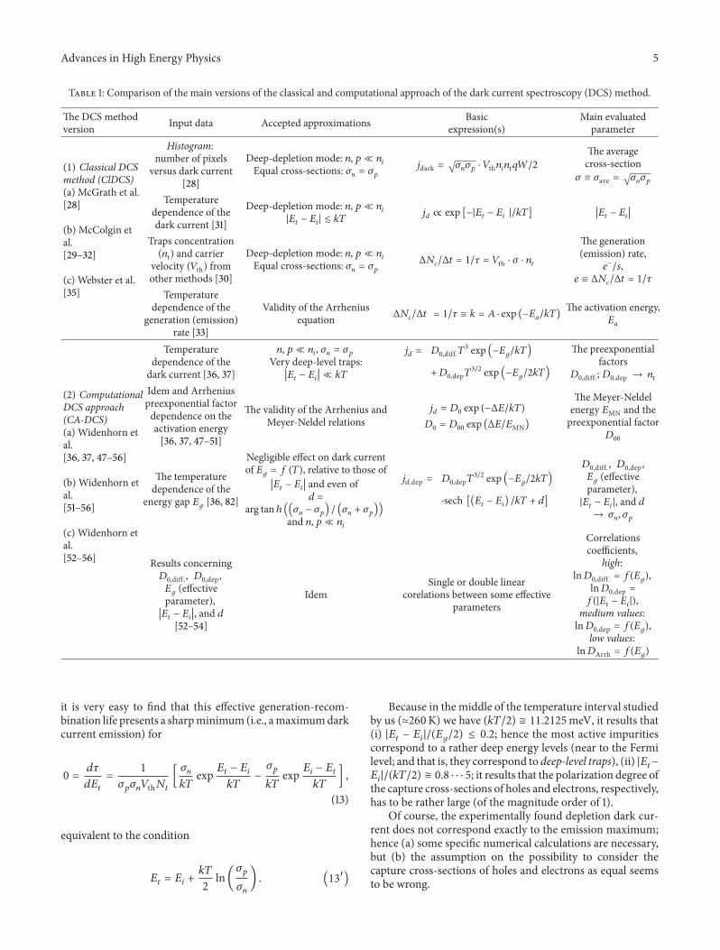
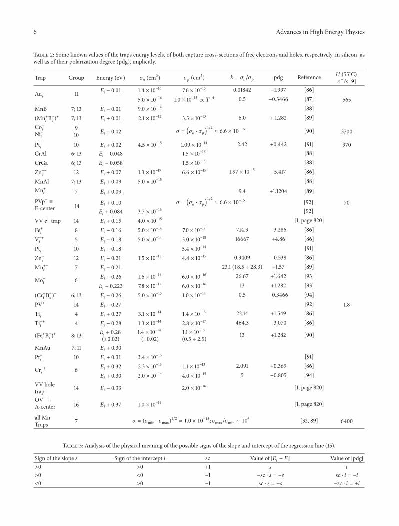
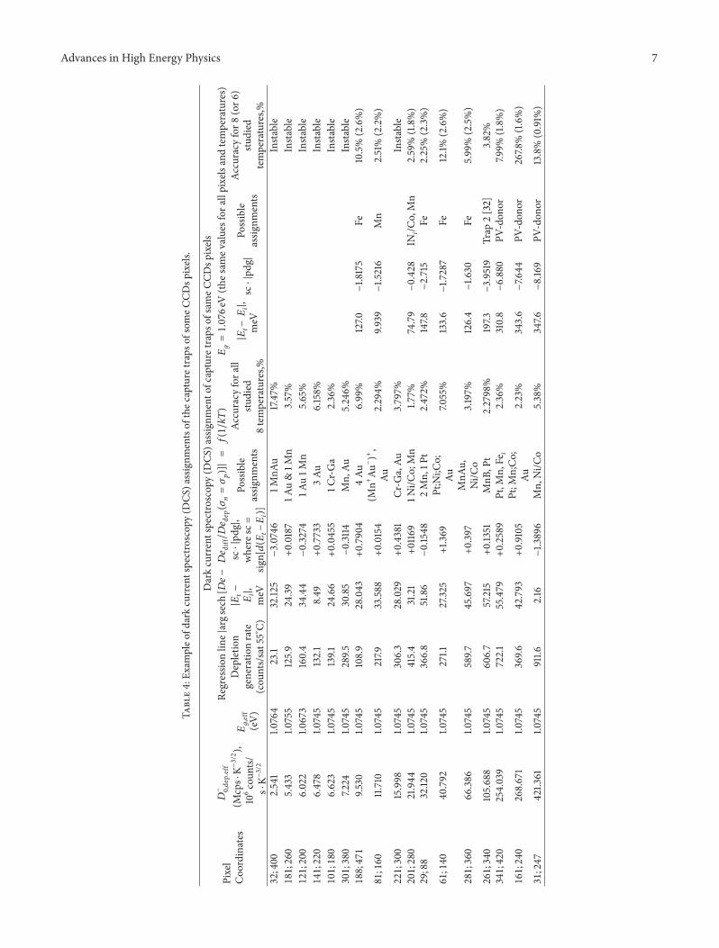