Embed Size (px)
Citation preview
January 18, 2010 20:33 International Journal of Electronics High-K-Logic-Gates-Revised
International Journal of ElectronicsVol. 00, No. 00, Month 200x, 1–19
RESEARCH ARTICLE
A Comparative Study on Gate Leakage and Performance of High-κNano-CMOS Logic Gates
Elias Kougianos and Saraju P. Mohanty(Received 00 Month 200x; final version received 00 Month 200x)
This paper provides a novel attempt to evaluate the gate leakage and delay characteristics of CMOS transis-tors and logic gates with various alternative high-κ gate dielectrics which are replacing SiO2 in traditionalnanoscale MOSFETs. Results have been obtained for both fixed as well as variable loads. The assumptionthat all gates drive the same load is considered in order to provide a fair comparison of the effect of thevariation of design and process parameters, especially that of different high-κ dielectrics on the gate directtunneling current and propagation delay. On the other hand, the variable loading effect considers a set ofpractical loading conditions for the logic gates. An exhaustive comparison of all cases finally presents a con-cluding evidence that the tunneling current is independent of loading conditions. On the other hand, there isan increase in the delay as the dielectric constant of gate material, and consequently the load on the device,increases. Ultimately, this paper presents fast and accurate models for on-the-fly calculation of tunnelingcurrent and delay with the aim of integrating them into design automation tools.
Keywords: Low-power design, gate leakage, leakage current, tunneling current, high-κ, nanoscale CMOS
1. Introduction and motivation
The demand for ever smaller and portable electronic devices has ultimately driven thescaling of CMOS towards its physical limits. Transistor feature sizes have dramaticallyshrunk with technology scaling and the value of gate oxide thickness (Tox) has reachedthe range of 12− 16A which is just a few mono-layers of SiO2. This trend is unavoidablein order to provide the required current drive in the presence of low supply voltages. Ithas led to a drastic change in the leakage components of the device both in the activeand inactive modes of operation. Consequently, the gate direct tunneling current Igate hasemerged as the most prominent form of leakage.
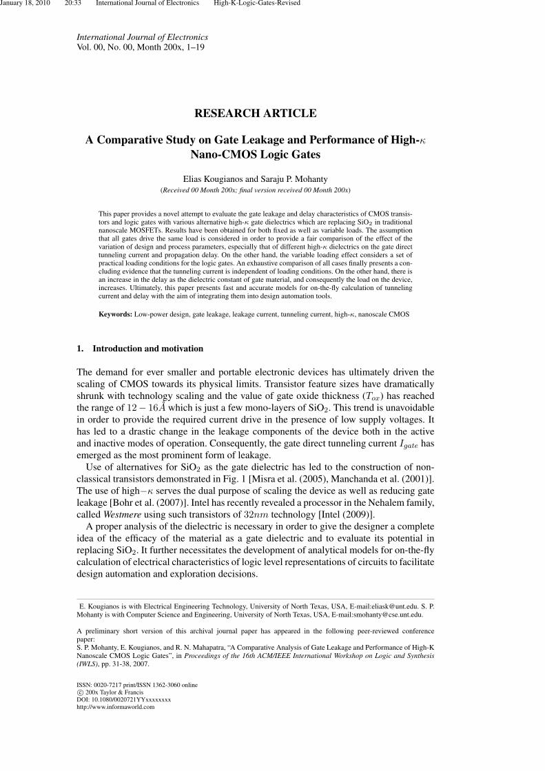
Use of alternatives for SiO2 as the gate dielectric has led to the construction of non-classical transistors demonstrated in Fig. 1 [Misra et al. (2005), Manchanda et al. (2001)].The use of high−κ serves the dual purpose of scaling the device as well as reducing gateleakage [Bohr et al. (2007)]. Intel has recently revealed a processor in the Nehalem family,called Westmere using such transistors of 32nm technology [Intel (2009)].
A proper analysis of the dielectric is necessary in order to give the designer a completeidea of the efficacy of the material as a gate dielectric and to evaluate its potential inreplacing SiO2. It further necessitates the development of analytical models for on-the-flycalculation of electrical characteristics of logic level representations of circuits to facilitatedesign automation and exploration decisions.
E. Kougianos is with Electrical Engineering Technology, University of North Texas, USA, E-mail:[email protected]. S. P.Mohanty is with Computer Science and Engineering, University of North Texas, USA, E-mail:[email protected].
A preliminary short version of this archival journal paper has appeared in the following peer-reviewed conferencepaper:S. P. Mohanty, E. Kougianos, and R. N. Mahapatra, “A Comparative Analysis of Gate Leakage and Performance of High-KNanoscale CMOS Logic Gates”, in Proceedings of the 16th ACM/IEEE International Workshop on Logic and Synthesis(IWLS), pp. 31-38, 2007.
ISSN: 0020-7217 print/ISSN 1362-3060 onlinec⃝ 200x Taylor & Francis
DOI: 10.1080/0020721YYxxxxxxxxhttp://www.informaworld.com
January 18, 2010 20:33 International Journal of Electronics High-K-Logic-Gates-Revised
2
n+ n+
P-Substrate
Drain
SiO2
(a) with SiO2 gate dielectric
n+ n+
P-Substrate
Drain
High-κ
(b) with high-κ gate dielectric
Figure 1. Nanoscale planar CMOS transistors: Classical versus non-classical
The rest of the paper is organized as follows. Section 2 summarizes contributions of thispaper and reviews important literature results relating to this work. In Section 3 we give anoverview of the major high-κ dielectric materials and their process technologies. In sec-tion 4 we present a complete transient study of logic gates. We present the characterizationof logic gates with respect to design and process parameters in Section 5. Analytical mod-eling of high-κ devices is presented in Section 6. The effect of load variation for high-κlogic gates is examined in 7. Applications of our analysis in terms of functional unit li-brary characterization and high level synthesis using high-κ cells are given in Section 8.Our findings and directions for future work are summarized in Section 9.
2. Contributions of this paper and related research
The replacement of SiO2 with a number of alternative dielectrics necessitates the de-velopment of an analytical method for on-the-fly calculation of electrical characteristicsof logic circuits. These analytical expressions will help in extending the benefits of de-sign automation involving traditional CMOS processes to design using alternative, non-traditional processes. This paper presents a novel characterization of high-κ nano-CMOSlogic gates and provides a complete analysis of the various associated design and processparameters in order to enhance the design process. The various contributions of this paperare as follows:
• A new approach is introduced for the characterization of high-κ dielectric CMOS tran-sistors and corresponding logic gates.
• A complete view of the design and process parameter variations of the devices is given,when high-κ gate dielectric materials are used.
• An exhaustive overview of the performance and characteristics of high-κ gates is pre-sented for both fixed and variable load.
• Novel analytical functions are given to provide on-the-fly calculations of the devicecharacteristics which would be a great tool for the design engineer for design space andtechnology exploration.
There has been extensive effort from academic as well as industrial research commu-nities to overcome the barriers to scaling of devices. This has extended from the domainof design and fabrication to the study of device physics and material science [Yang et al.(2003), Yu et al. (2002)]. Few research works exist for analysis and estimation of gateleakage in nano-CMOS circuits. In [Rao et al. (2003)], the authors presented mechanismsfor estimation of leakage. In [Lee et al. (2003)], a method is presented for analysis ofIgate. The authors in [Guindi and Najm (2003)] have formulated “state-dependent” gateleakage. The authors in [Agarwala et al. (2005)] have developed several methods of anal-ysis of total leakage. In [Mukhopadhyay et al. (2003)], the authors have studied the effectof gate tunneling current in ultra-thin gate oxide MOS devices. An analysis of the loadingeffect on leakage and a method of estimation of the total leakage in a logic circuit is pro-posed in [Mukhopadhyay et al. (2005)]. In [Maitra and Bhat (2003)], the authors propose
January 18, 2010 20:33 International Journal of Electronics High-K-Logic-Gates-Revised
3
analytical schemes to combine the channel and edge components of the gate oxide directtunneling current.
3. High−κ dielectrics in CMOS technology
3.1 Need for high-κ gate dielectrics
SiO2 has reached the fundamental limits in its role as the gate dielectric of choice [Karam-cheti et al. (2000)]. This is primarily due to the fact that decrease in the gate-oxide thick-ness is associated with a concomitant and significant increase in tunneling current. Thisinevitable drawback and the impending increase in leakage has called for alternativescandidates to replace SiO2. Such candidates need to have a higher dielectric constant thanSiO2 [Manchanda et al. (2001)].
3.2 Fabrication technology for high−κ
Several materials have been investigated for use in nano-CMOS technology, such as ZrO2,TiO2, BST, HfO2, Al2O3, SiON, and Si3N4 [Yang et al. (2003), Manchanda et al. (2001)].It is a challenging task in itself to integrate these materials into conventional CMOS pro-cesses [X. Guo and T. P. Ma (1998)]. Progress has been made in the development of vari-ous technologies for high-−κ gate dielectric deposition, but is still not in the mainstreamof fabrication [Huff et al. (2001), Kingon et al. (2000), Qi and et al. (2000)].
3.3 Compact modeling for high−κ
While the materials research is in progress, there is no research to address automatic de-sign and synthesis of systems using high-κ transistors. For compact modeling based studyof high-κ, non-classical transistors using the BSIM4/5 model, two possible options canbe considered: (i) varying the model parameter in the model card that denotes relativepermittivity (EPSROX) and/or (ii) finding the equivalent oxide thickness (EOT) for a di-electric under consideration. Approach (i) may not be sufficient to model the behavior ofnon-classic nano-CMOS with non-SiO2 dielectrics as it does not correctly account for thebarrier height of non-SiO2 dielectrics. Using method (ii) the EOT will be calculated so asto keep the ratio of relative permittivity over dielectric thickness constant.
Both of these approaches ignore several aspects of the physics behind non-SiO2 di-electrics, particularly in the Si/dielectric interface. However, in the absence of publisheddevice data, the methodology presented will provide meaningful information of the vari-ous materials under consideration for EDA applications.
We believe that along with the efforts in introducing high-κ gate dielectrics, futurephysical-aware low power synthesis methodologies should be developed in order to in-corporate them into existing automatic design or synthesis flows. This leads us to performextensive modeling, analysis and characterization of a number of high-κ dielectric CMOSlogic gates to facilitate design space exploration.
4. Analysis of logic gates
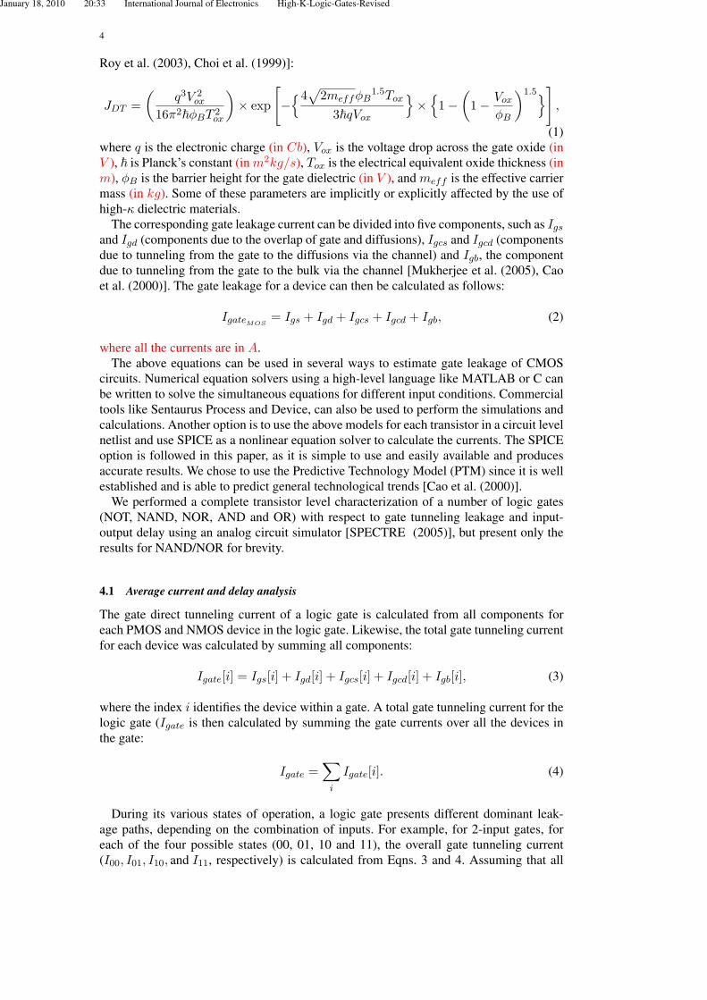
For direct tunneling, the tunneling probability of an electron is affected by the barrierheight, and the structure and thickness of the gate dielectric material. The tunneling cur-rent density of a MOS JDT (in A/m2) is expressed by [Mohanty and Kougianos (2006),
January 18, 2010 20:33 International Journal of Electronics High-K-Logic-Gates-Revised
4
Roy et al. (2003), Choi et al. (1999)]:
JDT =
(q3V 2
ox
16π2~ϕBT 2ox
)× exp
[−{4
√2meffϕB
1.5Tox
3~qVox
}×{1−
(1− Vox
ϕB
)1.5}],
(1)where q is the electronic charge (in Cb), Vox is the voltage drop across the gate oxide (inV ), ~ is Planck’s constant (in m2kg/s), Tox is the electrical equivalent oxide thickness (inm), ϕB is the barrier height for the gate dielectric (in V ), and meff is the effective carriermass (in kg). Some of these parameters are implicitly or explicitly affected by the use ofhigh-κ dielectric materials.
The corresponding gate leakage current can be divided into five components, such as Igsand Igd (components due to the overlap of gate and diffusions), Igcs and Igcd (componentsdue to tunneling from the gate to the diffusions via the channel) and Igb, the componentdue to tunneling from the gate to the bulk via the channel [Mukherjee et al. (2005), Caoet al. (2000)]. The gate leakage for a device can then be calculated as follows:
IgateMOS= Igs + Igd + Igcs + Igcd + Igb, (2)
where all the currents are in A.The above equations can be used in several ways to estimate gate leakage of CMOS
circuits. Numerical equation solvers using a high-level language like MATLAB or C canbe written to solve the simultaneous equations for different input conditions. Commercialtools like Sentaurus Process and Device, can also be used to perform the simulations andcalculations. Another option is to use the above models for each transistor in a circuit levelnetlist and use SPICE as a nonlinear equation solver to calculate the currents. The SPICEoption is followed in this paper, as it is simple to use and easily available and producesaccurate results. We chose to use the Predictive Technology Model (PTM) since it is wellestablished and is able to predict general technological trends [Cao et al. (2000)].
We performed a complete transistor level characterization of a number of logic gates(NOT, NAND, NOR, AND and OR) with respect to gate tunneling leakage and input-output delay using an analog circuit simulator [SPECTRE (2005)], but present only theresults for NAND/NOR for brevity.
4.1 Average current and delay analysis
The gate direct tunneling current of a logic gate is calculated from all components foreach PMOS and NMOS device in the logic gate. Likewise, the total gate tunneling currentfor each device was calculated by summing all components:
Igate[i] = Igs[i] + Igd[i] + Igcs[i] + Igcd[i] + Igb[i], (3)
where the index i identifies the device within a gate. A total gate tunneling current for thelogic gate (Igate is then calculated by summing the gate currents over all the devices inthe gate:
Igate =∑i
Igate[i]. (4)
During its various states of operation, a logic gate presents different dominant leak-age paths, depending on the combination of inputs. For example, for 2-input gates, foreach of the four possible states (00, 01, 10 and 11), the overall gate tunneling current(I00, I01, I10, and I11, respectively) is calculated from Eqns. 3 and 4. Assuming that all
January 18, 2010 20:33 International Journal of Electronics High-K-Logic-Gates-Revised
5
states are to occur with equal probability, an “average direct tunneling current” (Igate) iscalculated as :
Igate =
(I00 + I01 + I10 + I11
4
). (5)
On the other hand, the “peak tunneling current” can be defined as Ipeak =max(I00, I01, I10, I11).
While characterizing the gate leakage current we present its average value over vari-ous switching states of the logic gate. This ensures that we eliminate the effect of stacking.However, a state dependent look-up-table based gate leakage current approach can al-ways be used to facilitate its estimation in larger CMOS circuits.
Following standard approaches, we define the delay as the time difference between the50% level of the input and output waveforms Baker et al. (1998). For worst-case scenario,we chose the maximum delay time regardless of whether this was due to a low-to-high ora high-to-low transition.
A load value of 10 times the total gate capacitance Cgg of the PMOS device has beenchosen Mukherjee et al. (2005). In order to obtain a fair comparison of the performanceof the various dielectrics, without reference to a specific load, this value was calculatedfor a SiO2 device and kept fixed throughout the simulations.
4.2 Process and Design Parameters Variation
The BSIM 4.4 models generated represent a hypothetical 45nm CMOS process withoxide thickness Tox = 1.4nm, threshold voltage VTh = 0.22V for the NMOS andVTh = −0.22V for the PMOS. The nominal power supply is VDD = 0.7V . These mod-els are also scalable with respect to Tox and channel length. The effect of varying oxidethickness (Tox) was incorporated by varying TOXE in the spice model deck directly.The effect of varying dielectric material was modeled by calculating an equivalent oxidethickness (T ∗
ox) according to the formula:
T ∗ox =
(κSiO2
κgate
)× Tgate. (6)
In the above, κgate is the relative permittivity (dimensionless) and Tgate is the thicknessof the gate dielectric material (in m or A) other than SiO2, while κSiO2
is the relativepermittivity of SiO2 (=3.9). In this section we perform a parametric study for κ; howeverall real values of κ may not translate to a specific physical dielectric in nano-CMOS tech-nology. The length of the device is proportionately changed to minimize the impact ofhigher dielectric thickness on device performance and to maintain the per width gate ca-pacitance constant as per CMOS fabrication requirements [Taur (2002), Weste and Harris(2005)]. Thus, the scaling ratio of channel length to gate thickness is maintained constant.Moreover, the length and width of the transistors are chosen to maintain a
(WL
)ratio of
4 : 1 for NMOS and 8 : 1 for PMOS to ensure equal flow of current through the devicesand symmetric switching points. The variation of VDD is achieved by running a parametersweep in the simulator. Different simulation results for these variations are presented infigures 2 and 3.
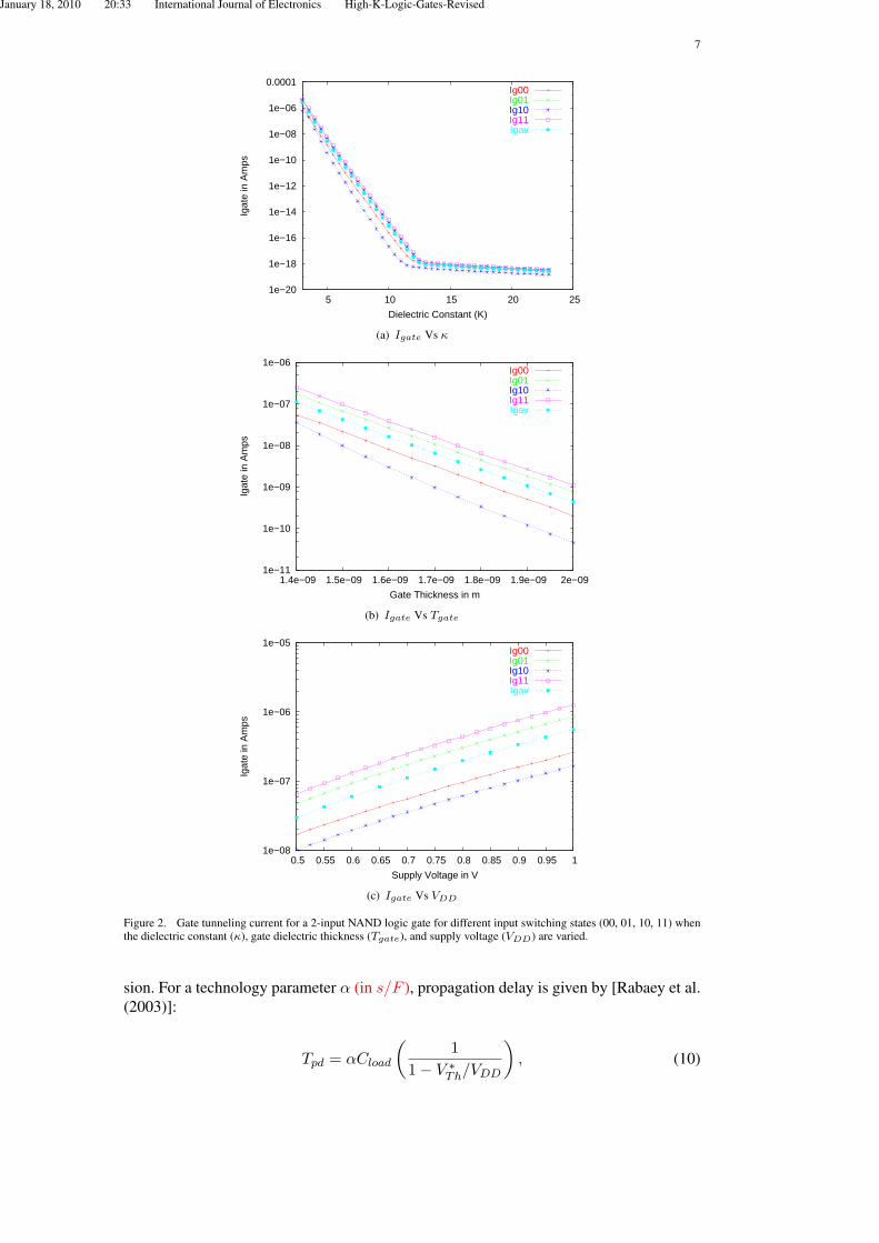
4.2.1 Effect of variation on tunneling current
It can be seen from Fig. 2(a) that with an increase in the value of κ there is a steadydecrease in the value of tunneling leakage, Igate. This trend continues up to a knee regionof κ = 12, after which all the components eventually become almost constant and thereis not much of a decrease in the value of Igate with an increase in κ. This indicates the
January 18, 2010 20:33 International Journal of Electronics High-K-Logic-Gates-Revised
6
presence of a saturation zone in the gate leakage versus κ characteristics which impliesthat there is not much benefit in deploying gate dielectrics of very high-κ (i. e. κ > 12)for gate tunneling leakage reduction in the 45nm node. The physical mechanism for thepresence of the knee can be seen by combining equations 1 and 6:
lnJDT ∼ −α lnκ− βκ, (7)
where α and β (both in ln(A/m2)) are positive, technology-dependent constants. Theknee occurs when the linear (second) term in equation 7 overtakes the logarithmic (first)component. Since the constants α and β depend on material parameters, it is expected thatthe knee region will vary for different technology nodes.
As can be seen from figure 2(b) there is a uniform decrease among all the componentsof the gate tunneling current with an increase in the gate thickness. However, this effectcan be utilized in some design styles as in dual-thickness approaches as an effective meansof minimizing the impact of gate tunneling leakage [Mohanty et al. (2006)].
Finally, ss can be seen from Fig. 2(c) an increase in the supply voltage leads to a cor-responding increase in the level of the gate tunneling leakage. This trend supports thescaling down of the supply voltage along with scaling of the device. Thus, supply voltagescaling can, to a certain extend, reduce gate leakage as well as dynamic power.
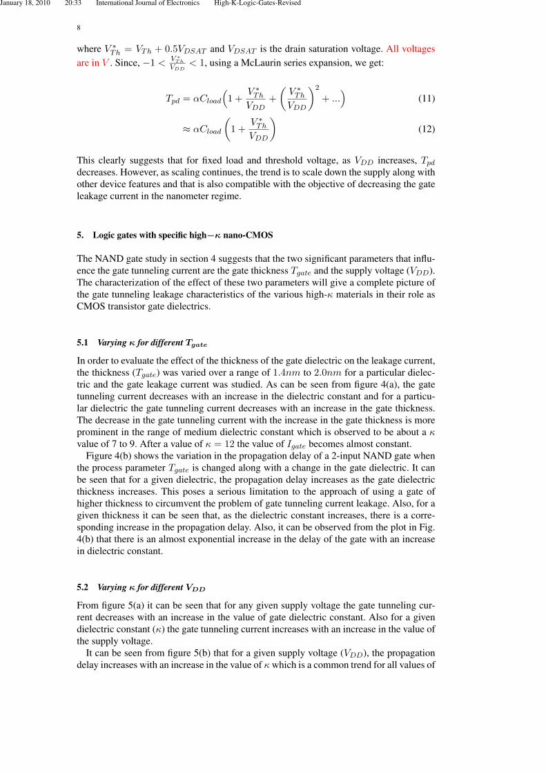
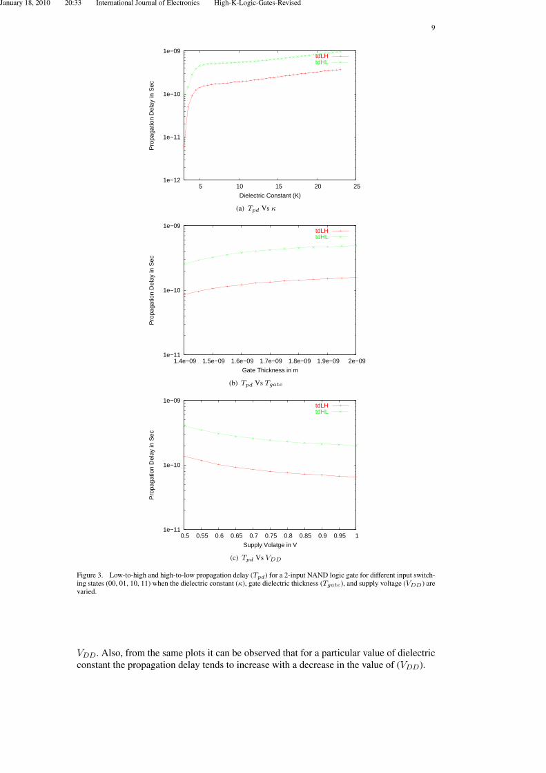
4.2.2 Effect of variation on propagation delay
The variation of Tpd is shown in Fig. 3(a), and demonstrates that there is a sharp in-crease in the value of Tpd with an increase in the gate dielectric constant. This increasecontinues until a value of around κ = 6 after which the slope is much lower. The increasein propagation delay can be attributed to the increase in capacitance per unit area (C
′
gate,in F/m2) of gate oxide with dielectric constant, i.e.,
C′
gate =
(κgateTgate
), (8)
while the presence of a “knee” region around κ ≃ 6 is due to similar behavior of Tpd asin equation 7.
The effect of variation of propagation delay with respect to the process parameter gatethickness shown in figure 3(b) indicates that there is an increase in the propagation delayof the gate as the gate thickness increases. This happens due to the increase in gate ca-pacitance (Cgate, in F ) with oxide thickness Tox (in m or nm) for a particular dielectric,say SiO2 with κ, as evident from the following discussion. The gate capacitance (Cgate)is given by [Weste and Harris (2005)]:
Cgate = ϵox
(L
Tox
)W = ϵox
(W
L
)(L
Tox
)L, (9)
where ϵox is the permittivity of the gate material (in F/m) and L and W are the lengthand width of the transistor (both in m or nm). Thus, as per the suggestion in [Taur (2002),Sultania et al. (2004), Weste and Harris (2005)], with increase in Tox when we maintain(
LTox
)and
(WL
)constant by increasing L, Cgate increases, and hence the propagation
delay. This result is consistent with the experimental results presented in [Sultania et al.(2004)], in the context of gate leakage reduction.
It can be observed from Fig. 3(c) that the propagation delay shows a decreasing trendwith an increase in the value of the supply voltage when κgate and Tgate are kept fixed.This is due to the increase in the drive current resulting from the increase in supply volt-age. However, a better insight of the situation can be obtained from the following discus-
January 18, 2010 20:33 International Journal of Electronics High-K-Logic-Gates-Revised
7
1e−20
1e−18
1e−16
1e−14
1e−12
1e−10
1e−08
1e−06
0.0001
5 10 15 20 25
Igat
e in
Am
ps
Dielectric Constant (K)
Ig00Ig01Ig10Ig11Igav
(a) Igate Vs κ
1e−11
1e−10
1e−09
1e−08
1e−07
1e−06
1.4e−09 1.5e−09 1.6e−09 1.7e−09 1.8e−09 1.9e−09 2e−09
Igat
e in
Am
ps
Gate Thickness in m
Ig00Ig01Ig10Ig11Igav
(b) Igate Vs Tgate
1e−08
1e−07
1e−06
1e−05
0.5 0.55 0.6 0.65 0.7 0.75 0.8 0.85 0.9 0.95 1
Igat
e in
Am
ps
Supply Voltage in V
Ig00Ig01Ig10Ig11Igav
(c) Igate Vs VDD
Figure 2. Gate tunneling current for a 2-input NAND logic gate for different input switching states (00, 01, 10, 11) whenthe dielectric constant (κ), gate dielectric thickness (Tgate), and supply voltage (VDD) are varied.
sion. For a technology parameter α (in s/F ), propagation delay is given by [Rabaey et al.(2003)]:
Tpd = αCload
(1
1− V ∗Th/VDD
), (10)
January 18, 2010 20:33 International Journal of Electronics High-K-Logic-Gates-Revised
8
where V ∗Th = VTh + 0.5VDSAT and VDSAT is the drain saturation voltage. All voltages
are in V . Since, −1 < V ∗Th
VDD< 1, using a McLaurin series expansion, we get:
Tpd = αCload
(1 +
V ∗Th
VDD+
(V ∗Th
VDD
)2
+ ...)
(11)
≈ αCload
(1 +
V ∗Th
VDD
)(12)
This clearly suggests that for fixed load and threshold voltage, as VDD increases, Tpd
decreases. However, as scaling continues, the trend is to scale down the supply along withother device features and that is also compatible with the objective of decreasing the gateleakage current in the nanometer regime.
5. Logic gates with specific high−κ nano-CMOS
The NAND gate study in section 4 suggests that the two significant parameters that influ-ence the gate tunneling current are the gate thickness Tgate and the supply voltage (VDD).The characterization of the effect of these two parameters will give a complete picture ofthe gate tunneling leakage characteristics of the various high-κ materials in their role asCMOS transistor gate dielectrics.
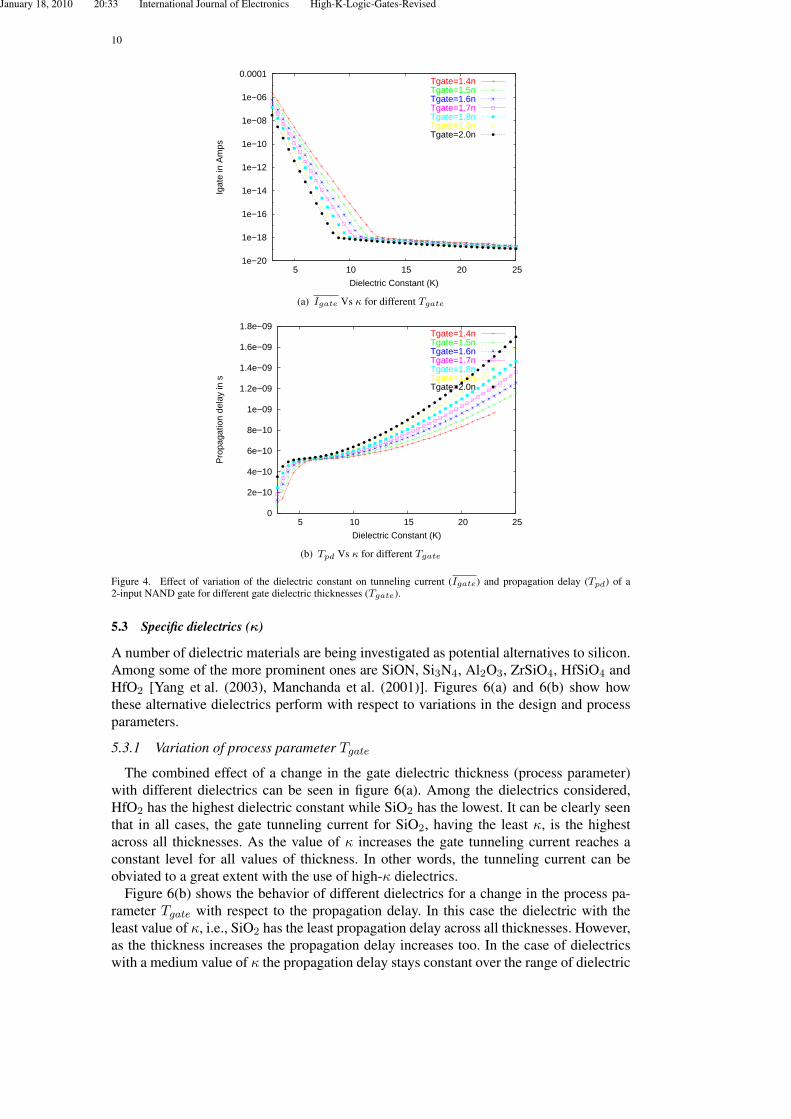
5.1 Varying κ for different Tgate
In order to evaluate the effect of the thickness of the gate dielectric on the leakage current,the thickness (Tgate) was varied over a range of 1.4nm to 2.0nm for a particular dielec-tric and the gate leakage current was studied. As can be seen from figure 4(a), the gatetunneling current decreases with an increase in the dielectric constant and for a particu-lar dielectric the gate tunneling current decreases with an increase in the gate thickness.The decrease in the gate tunneling current with the increase in the gate thickness is moreprominent in the range of medium dielectric constant which is observed to be about a κvalue of 7 to 9. After a value of κ = 12 the value of Igate becomes almost constant.
Figure 4(b) shows the variation in the propagation delay of a 2-input NAND gate whenthe process parameter Tgate is changed along with a change in the gate dielectric. It canbe seen that for a given dielectric, the propagation delay increases as the gate dielectricthickness increases. This poses a serious limitation to the approach of using a gate ofhigher thickness to circumvent the problem of gate tunneling current leakage. Also, for agiven thickness it can be seen that, as the dielectric constant increases, there is a corre-sponding increase in the propagation delay. Also, it can be observed from the plot in Fig.4(b) that there is an almost exponential increase in the delay of the gate with an increasein dielectric constant.
5.2 Varying κ for different VDD
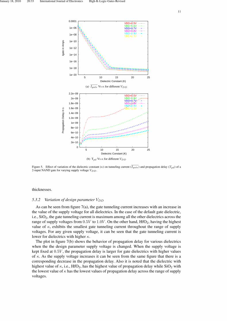
From figure 5(a) it can be seen that for any given supply voltage the gate tunneling cur-rent decreases with an increase in the value of gate dielectric constant. Also for a givendielectric constant (κ) the gate tunneling current increases with an increase in the value ofthe supply voltage.
It can be seen from figure 5(b) that for a given supply voltage (VDD), the propagationdelay increases with an increase in the value of κ which is a common trend for all values of
January 18, 2010 20:33 International Journal of Electronics High-K-Logic-Gates-Revised
9
1e−12
1e−11
1e−10
1e−09
5 10 15 20 25
Pro
paga
tion
Del
ay in
Sec
Dielectric Constant (K)
tdLHtdHL
(a) Tpd Vs κ
1e−11
1e−10
1e−09
1.4e−09 1.5e−09 1.6e−09 1.7e−09 1.8e−09 1.9e−09 2e−09
Pro
paga
tion
Del
ay in
Sec
Gate Thickness in m
tdLHtdHL
(b) Tpd Vs Tgate
1e−11
1e−10
1e−09
0.5 0.55 0.6 0.65 0.7 0.75 0.8 0.85 0.9 0.95 1
Pro
paga
tion
Del
ay in
Sec
Supply Volatge in V
tdLHtdHL
(c) Tpd Vs VDD
Figure 3. Low-to-high and high-to-low propagation delay (Tpd) for a 2-input NAND logic gate for different input switch-ing states (00, 01, 10, 11) when the dielectric constant (κ), gate dielectric thickness (Tgate), and supply voltage (VDD) arevaried.
VDD. Also, from the same plots it can be observed that for a particular value of dielectricconstant the propagation delay tends to increase with a decrease in the value of (VDD).
January 18, 2010 20:33 International Journal of Electronics High-K-Logic-Gates-Revised
10
1e−20
1e−18
1e−16
1e−14
1e−12
1e−10
1e−08
1e−06
0.0001
5 10 15 20 25
Igat
e in
Am
ps
Dielectric Constant (K)
Tgate=1.4nTgate=1.5nTgate=1.6nTgate=1.7nTgate=1.8nTgate=1.9nTgate=2.0n
(a) Igate Vs κ for different Tgate
0
2e−10
4e−10
6e−10
8e−10
1e−09
1.2e−09
1.4e−09
1.6e−09
1.8e−09
5 10 15 20 25
Pro
paga
tion
dela
y in
s
Dielectric Constant (K)
Tgate=1.4nTgate=1.5nTgate=1.6nTgate=1.7nTgate=1.8nTgate=1.9nTgate=2.0n
(b) Tpd Vs κ for different Tgate
Figure 4. Effect of variation of the dielectric constant on tunneling current (Igate) and propagation delay (Tpd) of a2-input NAND gate for different gate dielectric thicknesses (Tgate).
5.3 Specific dielectrics (κ)
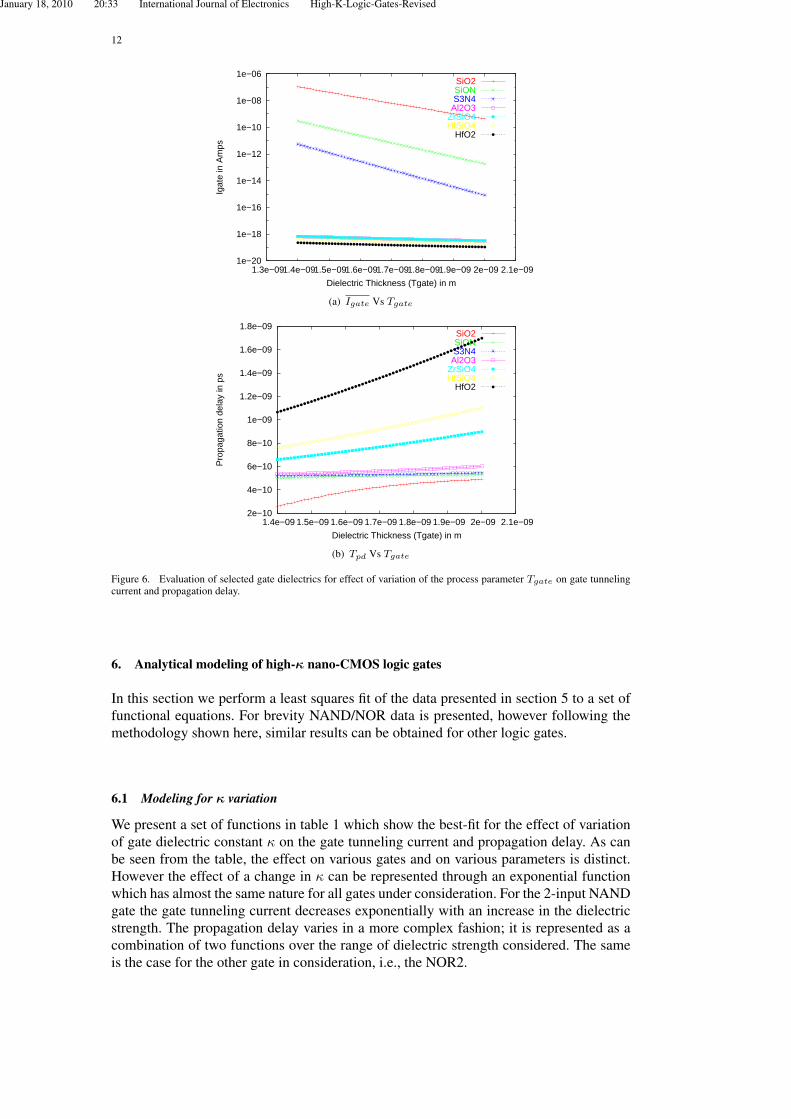
A number of dielectric materials are being investigated as potential alternatives to silicon.Among some of the more prominent ones are SiON, Si3N4, Al2O3, ZrSiO4, HfSiO4 andHfO2 [Yang et al. (2003), Manchanda et al. (2001)]. Figures 6(a) and 6(b) show howthese alternative dielectrics perform with respect to variations in the design and processparameters.
5.3.1 Variation of process parameter Tgate
The combined effect of a change in the gate dielectric thickness (process parameter)with different dielectrics can be seen in figure 6(a). Among the dielectrics considered,HfO2 has the highest dielectric constant while SiO2 has the lowest. It can be clearly seenthat in all cases, the gate tunneling current for SiO2, having the least κ, is the highestacross all thicknesses. As the value of κ increases the gate tunneling current reaches aconstant level for all values of thickness. In other words, the tunneling current can beobviated to a great extent with the use of high-κ dielectrics.
Figure 6(b) shows the behavior of different dielectrics for a change in the process pa-rameter Tgate with respect to the propagation delay. In this case the dielectric with theleast value of κ, i.e., SiO2 has the least propagation delay across all thicknesses. However,as the thickness increases the propagation delay increases too. In the case of dielectricswith a medium value of κ the propagation delay stays constant over the range of dielectric
January 18, 2010 20:33 International Journal of Electronics High-K-Logic-Gates-Revised
11
1e−20
1e−18
1e−16
1e−14
1e−12
1e−10
1e−08
1e−06
0.0001
5 10 15 20 25
Igat
e in
Am
ps
Dielectric Constant (K)
VDD=0.5VVDD=0.6VVDD=0.7VVDD=0.8VVDD=0.9VVDD=1.0V
(a) Igate Vs κ for different VDD
0
2e−10
4e−10
6e−10
8e−10
1e−09
1.2e−09
1.4e−09
1.6e−09
1.8e−09
2e−09
2.2e−09
5 10 15 20 25
Pro
paga
tion
Del
ay in
s
Dielectric Constant (K)
VDD=0.5VVDD=0.6VVDD=0.7VVDD=0.8VVDD=0.9VVDD=1.0V
(b) Tpd Vs κ for different VDD
Figure 5. Effect of variation of the dielectric constant (κ) on tunneling current (Igate) and propagation delay (Tpd) of a2-input NAND gate for varying supply voltage VDD .
thicknesses.
5.3.2 Variation of design parameter VDD
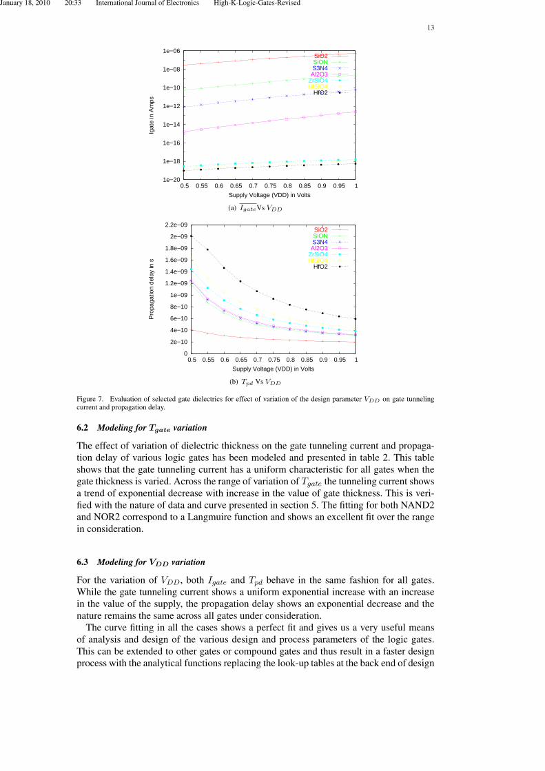
As can be seen from figure 7(a), the gate tunneling current increases with an increase inthe value of the supply voltage for all dielectrics. In the case of the default gate dielectric,i.e., SiO2, the gate tunneling current is maximum among all the other dielectrics across therange of supply voltages from 0.5V to 1.0V . On the other hand, HfO2, having the highestvalue of κ, exhibits the smallest gate tunneling current throughout the range of supplyvoltages. For any given supply voltage, it can be seen that the gate tunneling current islower for dielectrics with higher κ.
The plot in figure 7(b) shows the behavior of propagation delay for various dielectricswhen the the design parameter supply voltage is changed. When the supply voltage iskept fixed at 0.5V , the propagation delay is larger for gate dielectrics with higher valuesof κ. As the supply voltage increases it can be seen from the same figure that there is acorresponding decrease in the propagation delay. Also it is noted that the dielectric withhighest value of κ, i.e., HfO2, has the highest value of propagation delay while SiO2 withthe lowest value of κ has the lowest values of propagation delay across the range of supplyvoltages.
January 18, 2010 20:33 International Journal of Electronics High-K-Logic-Gates-Revised
12
1e−20
1e−18
1e−16
1e−14
1e−12
1e−10
1e−08
1e−06
1.3e−09 1.4e−09 1.5e−09 1.6e−09 1.7e−09 1.8e−09 1.9e−09 2e−09 2.1e−09
Igat
e in
Am
ps
Dielectric Thickness (Tgate) in m
SiO2SiONS3N4
Al2O3ZrSiO4HfSiO4
HfO2
(a) Igate Vs Tgate
2e−10
4e−10
6e−10
8e−10
1e−09
1.2e−09
1.4e−09
1.6e−09
1.8e−09
1.4e−09 1.5e−09 1.6e−09 1.7e−09 1.8e−09 1.9e−09 2e−09 2.1e−09
Pro
paga
tion
dela
y in
ps
Dielectric Thickness (Tgate) in m
SiO2SiONS3N4
Al2O3ZrSiO4HfSiO4
HfO2
(b) Tpd Vs Tgate
Figure 6. Evaluation of selected gate dielectrics for effect of variation of the process parameter Tgate on gate tunnelingcurrent and propagation delay.
6. Analytical modeling of high-κ nano-CMOS logic gates
In this section we perform a least squares fit of the data presented in section 5 to a set offunctional equations. For brevity NAND/NOR data is presented, however following themethodology shown here, similar results can be obtained for other logic gates.
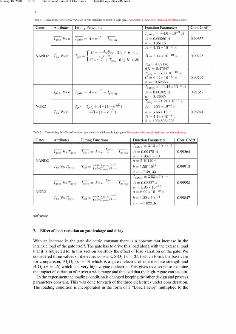
6.1 Modeling for κ variation
We present a set of functions in table 1 which show the best-fit for the effect of variationof gate dielectric constant κ on the gate tunneling current and propagation delay. As canbe seen from the table, the effect on various gates and on various parameters is distinct.However the effect of a change in κ can be represented through an exponential functionwhich has almost the same nature for all gates under consideration. For the 2-input NANDgate the gate tunneling current decreases exponentially with an increase in the dielectricstrength. The propagation delay varies in a more complex fashion; it is represented as acombination of two functions over the range of dielectric strength considered. The sameis the case for the other gate in consideration, i.e., the NOR2.
January 18, 2010 20:33 International Journal of Electronics High-K-Logic-Gates-Revised
13
1e−20
1e−18
1e−16
1e−14
1e−12
1e−10
1e−08
1e−06
0.5 0.55 0.6 0.65 0.7 0.75 0.8 0.85 0.9 0.95 1
Igat
e in
Am
ps
Supply Voltage (VDD) in Volts
SiO2SiONS3N4
Al2O3ZrSiO4HfSiO4
HfO2
(a) IgateVs VDD
0
2e−10
4e−10
6e−10
8e−10
1e−09
1.2e−09
1.4e−09
1.6e−09
1.8e−09
2e−09
2.2e−09
0.5 0.55 0.6 0.65 0.7 0.75 0.8 0.85 0.9 0.95 1
Pro
paga
tion
dela
y in
s
Supply Voltage (VDD) in Volts
SiO2SiONS3N4
Al2O3ZrSiO4HfSiO4
HfO2
(b) Tpd Vs VDD
Figure 7. Evaluation of selected gate dielectrics for effect of variation of the design parameter VDD on gate tunnelingcurrent and propagation delay.
6.2 Modeling for Tgate variation
The effect of variation of dielectric thickness on the gate tunneling current and propaga-tion delay of various logic gates has been modeled and presented in table 2. This tableshows that the gate tunneling current has a uniform characteristic for all gates when thegate thickness is varied. Across the range of variation of Tgate the tunneling current showsa trend of exponential decrease with increase in the value of gate thickness. This is veri-fied with the nature of data and curve presented in section 5. The fitting for both NAND2and NOR2 correspond to a Langmuire function and shows an excellent fit over the rangein consideration.
6.3 Modeling for VDD variation
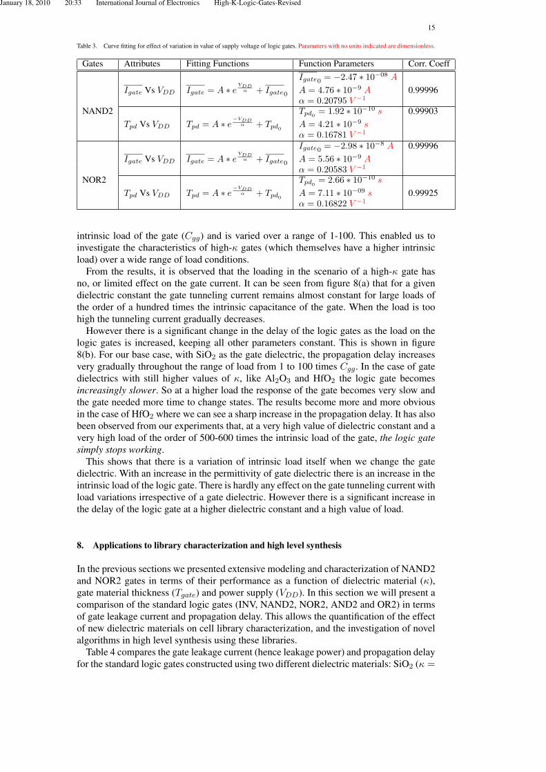
For the variation of VDD, both Igate and Tpd behave in the same fashion for all gates.While the gate tunneling current shows a uniform exponential increase with an increasein the value of the supply, the propagation delay shows an exponential decrease and thenature remains the same across all gates under consideration.
The curve fitting in all the cases shows a perfect fit and gives us a very useful meansof analysis and design of the various design and process parameters of the logic gates.This can be extended to other gates or compound gates and thus result in a faster designprocess with the analytical functions replacing the look-up tables at the back end of design
January 18, 2010 20:33 International Journal of Electronics High-K-Logic-Gates-Revised
14
Table 1. Curve fitting for effect of variation in gate dielectric constant in logic gates. Parameters with no units indicated are dimensionless.
Gates Attributes Fitting Functions Function Parameters Corr. CoeffIgate0 = −4.6 ∗ 10−9 A
Igate Vs κ Igate = A ∗ e−Kα + Igate0 A = 0.00966 A 0.99655
α = 0.36115A = 4.12 ∗ 10−11 s
NAND2 Tpd Vs κ Tpd =
{B + A−B
1+eK−K0
dK
, 2.5 ≤ K < 6
C ∗ e−Kα + Tpd0
, 6 ≤ K < 30B = 5.14 ∗ 10−10 s 0.99725
K0 = 4.02176dK = 0.47847Tpd0
= 3.75 ∗ 10−10 sC = 6.94 ∗ 10−11 s 0.99797α = 10.62653Igate0 = −1.42 ∗ 10−8 A
Igate Vs κ Igate = A ∗ e−Kα + Igate0 A = 0.00302 A 0.97657
α = 0.43885Tpd0
= −1.21 ∗ 10−8 s
NOR2 Tpd = Tpd0+A ∗ (1− e
−Kα ) A = 1.23 ∗ 10−8 s
Tpd Vs κ +B ∗ (1− e−Kβ ) α = 6.66 ∗ 10−1 0.96941
B = 1.13 ∗ 10−1 sβ = 10548034228
Table 2. Curve fitting for effect of variation gate dielectric thickness in logic gates. Parameters with no units indicated are dimensionless.
Gates Attributes Fitting Functions Function Parameters Corr. CoeffIgate0 = 3.13 ∗ 10−10 A
Igate Vs Tgate Igate = A ∗ e−Tgate
α + Igate0 A = 0.09475 A 0.99564α = 1.03E − 10
NAND2 a = 5.1011010
Tpd Vs Tgate Tpd =a∗b∗(Tgate)
(1−c)
1+b∗(Tgate)(1−c) b = 1.5011075 0.99913c = −7.49133Igate0 = 3.53 ∗ 10−10
Igate Vs Tgate Igate = A ∗ e−Tgate
α + Igate0 A = 0.08227 s 0.99998α = 1.05 ∗ 10−10
NOR2 a = 6.99 ∗ 10−10 s
Tpd Vs Tgate Tpd =a∗b∗(Tgate)
(1−c)
1+b∗(Tgate)(1−c) b = 1.22 ∗ 10+71 0.99847c = −7.02216
software.
7. Effect of load variation on gate leakage and delay
With an increase in the gate dielectric constant there is a concomitant increase in theintrinsic load of the gate itself. The gate has to drive this load along with the external loadthat it is subjected to. In this section we study the effect of load variation on the gate. Weconsidered three values of dielectric constant, SiO2 (κ = 3.9) which forms the base casefor comparison, Al2O3 (κ = 9) which is a gate dielectric of intermediate strength andHfO2 (κ = 25) which is a very high-κ gate dielectric. This gives us a scope to examinethe impact of variation of κ over a wide range and the load that the high-κ gate can sustain.
In the experiment the loading condition is changed keeping the other design and processparameters constant. This was done for each of the three dielectrics under consideration.The loading condition is incorporated in the form of a “Load Factor” multiplied to the
January 18, 2010 20:33 International Journal of Electronics High-K-Logic-Gates-Revised
15
Table 3. Curve fitting for effect of variation in value of supply voltage of logic gates. Parameters with no units indicated are dimensionless.
Gates Attributes Fitting Functions Function Parameters Corr. CoeffIgate0 = −2.47 ∗ 10−08 A
Igate Vs VDD Igate = A ∗ eVDD
α + Igate0 A = 4.76 ∗ 10−9 A 0.99996α = 0.20795 V −1
NAND2 Tpd0= 1.92 ∗ 10−10 s 0.99903
Tpd Vs VDD Tpd = A ∗ e−VDD
α + Tpd0A = 4.21 ∗ 10−9 sα = 0.16781 V −1
Igate0 = −2.98 ∗ 10−8 A 0.99996Igate Vs VDD Igate = A ∗ e
VDDα + Igate0 A = 5.56 ∗ 10−9 A
α = 0.20583 V −1
NOR2 Tpd0= 2.66 ∗ 10−10 s
Tpd Vs VDD Tpd = A ∗ e−VDD
α + Tpd0A = 7.11 ∗ 10−09 s 0.99925α = 0.16822 V −1
intrinsic load of the gate (Cgg) and is varied over a range of 1-100. This enabled us toinvestigate the characteristics of high-κ gates (which themselves have a higher intrinsicload) over a wide range of load conditions.
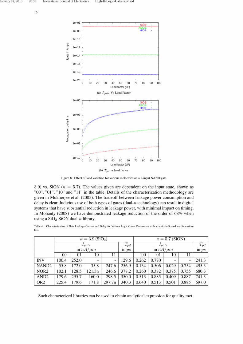
From the results, it is observed that the loading in the scenario of a high-κ gate hasno, or limited effect on the gate current. It can be seen from figure 8(a) that for a givendielectric constant the gate tunneling current remains almost constant for large loads ofthe order of a hundred times the intrinsic capacitance of the gate. When the load is toohigh the tunneling current gradually decreases.
However there is a significant change in the delay of the logic gates as the load on thelogic gates is increased, keeping all other parameters constant. This is shown in figure8(b). For our base case, with SiO2 as the gate dielectric, the propagation delay increasesvery gradually throughout the range of load from 1 to 100 times Cgg. In the case of gatedielectrics with still higher values of κ, like Al2O3 and HfO2 the logic gate becomesincreasingly slower. So at a higher load the response of the gate becomes very slow andthe gate needed more time to change states. The results become more and more obviousin the case of HfO2 where we can see a sharp increase in the propagation delay. It has alsobeen observed from our experiments that, at a very high value of dielectric constant and avery high load of the order of 500-600 times the intrinsic load of the gate, the logic gatesimply stops working.
This shows that there is a variation of intrinsic load itself when we change the gatedielectric. With an increase in the permittivity of gate dielectric there is an increase in theintrinsic load of the logic gate. There is hardly any effect on the gate tunneling current withload variations irrespective of a gate dielectric. However there is a significant increase inthe delay of the logic gate at a higher dielectric constant and a high value of load.
8. Applications to library characterization and high level synthesis
In the previous sections we presented extensive modeling and characterization of NAND2and NOR2 gates in terms of their performance as a function of dielectric material (κ),gate material thickness (Tgate) and power supply (VDD). In this section we will present acomparison of the standard logic gates (INV, NAND2, NOR2, AND2 and OR2) in termsof gate leakage current and propagation delay. This allows the quantification of the effectof new dielectric materials on cell library characterization, and the investigation of novelalgorithms in high level synthesis using these libraries.
Table 4 compares the gate leakage current (hence leakage power) and propagation delayfor the standard logic gates constructed using two different dielectric materials: SiO2 (κ =
January 18, 2010 20:33 International Journal of Electronics High-K-Logic-Gates-Revised
16
1e−20
1e−18
1e−16
1e−14
1e−12
1e−10
1e−08
1e−06
0 10 20 30 40 50 60 70 80 90 100
Igat
e in
Am
ps
Load factor (LF)
SiO2Al2O3HfO2
(a) Igate Vs Load Factor
1e−10
1e−09
1e−08
1e−07
1e−06
0 10 20 30 40 50 60 70 80 90 100
Pro
paga
tion
dela
y in
s
Load factor (LF)
SiO2Al2O3HfO2
(b) Tpd vs load factor
Figure 8. Effect of load variation for various dielectrics on a 2-input NAND gate.
3.9) vs. SiON (κ = 5.7). The values given are dependent on the input state, shown as”00”, ”01”, ”10” and ”11” in the table. Details of the characterization methodology aregiven in Mukherjee et al. (2005). The tradeoff between leakage power consumption anddelay is clear. Judicious use of both types of gates (dual-κ technology) can result in digitalsystems that have substantial reduction in leakage power, with minimal impact on timing.In Mohanty (2008) we have demonstrated leakage reduction of the order of 68% whenusing a SiO2-SiON dual-κ library.
Table 4. Characterization of Gate Leakage Current and Delay for Various Logic Gates. Parameters with no units indicated are dimension-less.
κ = 3.9 (SiO2) κ = 5.7 (SiON)Igate Tpd Igate Tpd
in nA/µm in ps in nA/µm in ps00 01 10 11 00 01 10 11
INV 100.4 252.0 - - 129.6 0.262 0.770 - - 241.3NAND2 55.8 172.0 35.8 247.6 256.9 0.134 0.506 0.029 0.754 495.3NOR2 102.1 128.5 121.3n 246.6 378.2 0.260 0.382 0.375 0.755 680.3AND2 179.6 295.7 160.0 298.5 350.0 0.513 0.885 0.409 0.887 741.3OR2 225.4 179.6 171.8 297.7n 340.3 0.640 0.513 0.501 0.885 697.0
Such characterized libraries can be used to obtain analytical expression for quality met-
January 18, 2010 20:33 International Journal of Electronics High-K-Logic-Gates-Revised
REFERENCES 17
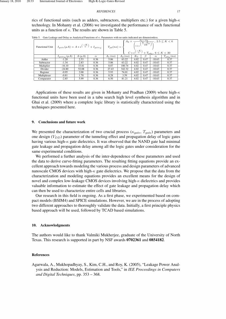
rics of functional units (such as adders, subtractors, multipliers etc.) for a given high-κtechnology. In Mohanty et al. (2006) we investigated the performance of such functionalunits as a function of κ. The results are shown in Table 5.
Table 5. Gate Leakage and Delay as Analytical Functions of κ. Parameters with no units indicated are dimensionless.
Functional Unit Igate(µA) = A ∗ e
(−Kα
)+ Igate0 Tpd(ns) =
A2 +
A1−A21+e
(K−K0
dK
), 2.5 ≤ K < 6
C ∗ e
(−Kα
)+ Tpd0
, 6 ≤ K < 30Igate0 (µA) A (µA) α A1 (ns) A2 (ns) K0 β α Tpd0
(ns)Adder -1.20 2.53 0.36 5.06 63.22 4.02 0.47 -10.63 0.37
Subtractor -1.34 2.83 0.36 5.06 63.22 4.02 0.47 -10.63 0.37Multiplier -16.10 33.81 0.36 8.07 100.74 4.02 0.47 -10.63 0.37
Divider -24.80 52.08 0.36 27.43 342.32 4.02 0.47 -10.63 0.37Register -0.95 2.00 0.36 5.93 74.01 4.02 0.47 -10.63 0.37
Multiplexer -0.81 1.70 0.36 0.28 3.59 4.02 0.47 -10.63 0.37Comparator -2.85 5.99 0.36 6.50 81.21 4.02 0.47 -10.63 0.37
Applications of these results are given in Mohanty and Pradhan (2009) where high-κfunctional units have been used in a tabu search high level synthesis algorithm and inGhai et al. (2009) where a complete logic library is statistically characterized using thetechniques presented here.
9. Conclusions and future work
We presented the characterization of two crucial process (κgate, Tgate) parameters andone design (VDD) parameter of the tunneling effect and propagation delay of logic gateshaving various high-κ gate dielectrics. It was observed that the NAND gate had minimalgate leakage and propagation delay among all the logic gates under consideration for thesame experimental conditions.
We performed a further analysis of the inter-dependence of these parameters and usedthe data to derive curve-fitting parameters. The resulting fitting equations provide an ex-cellent approach towards modeling the various process and design parameters of advancednanoscale CMOS devices with high-κ gate dielectrics. We propose that the data from thecharacterization and modeling equations provides an excellent means for the design ofnovel and complex low-leakage CMOS devices involving high-κ dielectrics and providesvaluable information to estimate the effect of gate leakage and propagation delay whichcan then be used to characterize entire cells and libraries.
Our research in this field is ongoing. As a first phase, we experimented based on com-pact models (BSIM4) and SPICE simulations. However, we are in the process of adoptingtwo different approaches to thoroughly validate the data. Initially, a first principle physicsbased approach will be used, followed by TCAD based simulations.
10. Acknowledgments
The authors would like to thank Valmiki Mukherjee, graduate of the University of NorthTexas. This research is supported in part by NSF awards 0702361 and 0854182.
References
Agarwala, A., Mukhopadhyay, S., Kim, C.H., and Roy, K. (2005), “Leakage Power Anal-ysis and Reduction: Models, Estimation and Tools,” in IEE Proceedings in Computersand Digital Techniques, pp. 353 – 368.
January 18, 2010 20:33 International Journal of Electronics High-K-Logic-Gates-Revised
18 REFERENCES
Baker, R.J., Li, H.W., and Boyce, D.E., CMOS: Circuit Design, layout, and Simulation,IEEE Press (1998).
Bohr, M.T., Chau, R.S., Ghani, T., and Mistry, K. (2007), “The High-κ Solution,” IEEESpectrum, 44(10), 29 – 35.
Cao, Y., Sato, T., Sylvester, D., Orshansky, M., and Hu, C. (2000), “New Paradigm of Pre-dictive MOSFET and Interconnect Modeling for Early Circuit Design,” in Proceedingsof the IEEE Custom Integrated Circuits Conference, pp. 201–204.
Choi, C.H., Oh, K.H., Goo, J.S., Yu, Z., and Dutton, R.W. (1999), “Direct TunnelingCurrent Model for Circuit Simulation,” IEEE Electronic Devices Meeting - TechnicalDigest, pp. 735–738.
Ghai, D., Mohanty, S.P., Kougianos, E. and Patra, D. (2009), “A PVT Aware AccurateStatistical Logic Library for High-κ Metal-Gate Nano-CMOS,” in Proceedings of the10th IEEE International Symposium on Quality Electronic Design (ISQED), pp. 47–54.
Guindi, R., and Najm, F. (2003), “Design Techniques for Gate-Leakage Reduction inCMOS Circuits,” in International Symposium On Quality Electronic Design.
X. Guo and T. P. Ma, (1998), “Tunneling Leakage Current in Oxynitride: Dependence onOxygen/Nitrogen Content,” IEEE Electron Device Letters, 19(6), 207–209.
H. R. Huff (2001), “Integration of high-k Gate Stack Systems into Planar CMOS ProcessFlows,” in International Workshop on Gate Insulators, pp. 2–11.
Intel Corp.,“Intel demos first-ever 32nm processors,” http://www.engadget.com/2009/02/10/intel-demos-first-ever-32nm-processors/ (2009).
Lee, D., Kwong, W., Blaauw, D., and Sylvester, D. (2003), “Simultaneous Subthresholdand Gate-Oxide Tunneling Leakage Current Analysis in Nanometer CMOS Design.,”in International Symposium on Quality Electronic Design, pp. 287–292.
Karamcheti, A., Watt, V.H.C., Al-Shareef, H.N., Luo, T.Y., Brown, G.A., Jackson, M.D.,and Huff, H.R. (2000), “Silicon Oxynitride Films as Segue to the High-K Era,” Semi-conductor Fabtech, 12, 207–214.
Kingon, A.I., Maria, J.P., and Streifferr, S.K. (2000), “Alternative Dielectrics to SiliconDioxide for Memory and Logic Devices,” Nature, 406, 1021–1038.
Maitra, K., and Bhat, N. (2003), “Analytical Approach to Integrate the Different Compo-nents of Direct Tunneling Current Through Ultrathin Gate Oxides in n-Channel Metal-Oxide-Semiconductor Field-Effect Transistors,” Journal of Applied Physics, 9348(2),1064–1068.
Manchanda, L., Busch, B., Green, M.L., Morris, M., van Dover, R.B., Kwo, R., and Arava-mudhan, S. (2001), “High K gate Dielectrics for the Silicon Industry,” in InternationalWorkshop on Gate Insulators, pp. 56–60.
Misra, D., Iwai, H., and Wong, H. (2005), “High−κ Gate Dielectrics,” The Electrochemi-cal Society Interface, 14(2), 30–34.
Mohanty, S.P., and Kougianos, E. (2006), “Modeling and Reduction of Gate Leakageduring Behavioral Synthesis of NanoCMOS Circuits,” in Proceedings of the 19th IEEEInternational Conference on VLSI Design (VLSID), pp. 83–88.
Mohanty, S.P., Velagapudi, R., and Kougianos, E. (2006), “Dual-K Versus Dual-T Tech-nique for Gate Leakage Reduction: A Comparative Perspective,” in Proceedings of the7th IEEE International Symposium on Quality Electronic Design (ISQED), pp. 564–569.
Mohanty, S.P. (2008), “ILP Based gate Leakage Optimization using DKCMOS Libraryduring RTL Synthesis,” in Proceedings of the 9th IEEE International Symposium onQuality Electronic Design (ISQED), pp. 174–177.
Mohanty, S.P., and Pradhan, D.K.(2009), “Tabu Search Based Gate Leakage Optimizationusing DKCMOS Library in Architecture Synthesis,” in Proceedings of the 12th IEEEInternational Conference on Information Technology (ICIT), pp. 3–9.
Mukherjee, V., Mohanty, S.P., and Kougianos, E. (2005), “A Dual Dielectric Approach
January 18, 2010 20:33 International Journal of Electronics High-K-Logic-Gates-Revised
REFERENCES 19
for Performance Aware Gate Tunneling Reduction in Combinational Circuits,” in Pro-ceedings of the 23rd IEEE International Conference of Computer Design (ICCD), pp.431–436.
Mukhopadhyay, S., Neau, C., R, T.C., Agarwala, A., Kim, C., and Roy, K. (2003), “Gateleakage reduction for scaled devices using transistor stacking,” IEEE Transactions onVery Large Scale Integration (VLSI) Systems, 11(4), 716 – 730.
Mukhopadhyay, S., Bhunia, S., and Roy, K. (2005), “Modeling and Analysis of LoadingEffect on Leakage of Nano-Scaled Bulk-CMOS Logic Circuits,” in Proceedings of theConference on Design, Automation and Test in Europe , pp. 224 – 229.
Qi, W.J., and et al., (2000), “Ultrathin Zirconium Silicate Film With Good Thermal Sta-bility for Alternative Gate Dielectric Application,” Applied Physics Letters, 77, 1704–1706.
Rabaey, J.M., Chandrakasan, A., and Nikolic, B., Digital Integrated Circuits, PrenticeHall (2003).
Rao, R.M., Burns, J.L., Devgan, A., and Brown, R.B. (2003), “Efficient techniques forgate leakage estimation,” in International Symposium on Low Power Devices”, pp.100–103.
Roy, K., Mukhopadhyay, S., and Meimand, H.M. (2003), “Leakage Current Mechanismsand Leakage Reduction Techniques in Deep-Submicrometer CMOS Circuits,” Pro-ceedings of the IEEE, 91(2), 305–327.
SPECTRE, Spectre Circuit Simulator User’s Guide (2005).Sultania, A.K., Sylvester, D., and Sapatnekar, S.S. (2004), “Tradeoffs Between Gate Ox-
ide Leakage and Delay for Dual Tox Circuits,” in Proceedings of Design AutomationConference, pp. 761–766.
Taur, Y. (2002), “CMOS design near the limit of scaling,” IBM Journal on Research andDevelopment, 46(2/3), 235–244.
Weste, N.H.E., and Harris, D., CMOS VLSI Design : A Circuit and Systems Perspective,Addison Wesley (2005).
Yang, M., Gusev, E.P., Ieong, M., Gluschenkov, O., Boyd, D.C., Chan, K.K., Kozlowsky,P.M., D’Emic, C.P., Sicina, R.M., Jamison, P.C., and Chou, A.I. (2003), “PerformanceDependence of CMOS on Silicon Substrate Orientation for Ultrathin and HfO2 GateDielectrics,” IEEE Electron Device Letters, 24(5), 339–341.
Yu, H.Y., Hou, Y.T., Li, M.F., and Kwong, D.-L. (2002), “Hole Tunneling CurrentThrough Oxynitride/Oxide Stack and the Stack Optimization for p-MOSFETs,” inIEEE Electron Device letters, 23(5), pp. 285–290.


