Embed Size (px)
Citation preview

Core and valence exciton formation in x-ray absorption, x-ray emission and x-ray excited
optical luminescence from passivated Si nanocrystals at the Si L2,3 edge
This article has been downloaded from IOPscience. Please scroll down to see the full text article.
2009 J. Phys.: Condens. Matter 21 095005
(http://iopscience.iop.org/0953-8984/21/9/095005)
Download details:
IP Address: 129.234.188.75
The article was downloaded on 23/08/2010 at 15:05
Please note that terms and conditions apply.
View the table of contents for this issue, or go to the journal homepage for more
Home Search Collections Journals About Contact us My IOPscience

IOP PUBLISHING JOURNAL OF PHYSICS: CONDENSED MATTER
J. Phys.: Condens. Matter 21 (2009) 095005 (8pp) doi:10.1088/0953-8984/21/9/095005
Core and valence exciton formation inx-ray absorption, x-ray emission and x-rayexcited optical luminescence frompassivated Si nanocrystals at the Si L2,3edge
L Siller1,5, S Krishnamurthy1, L Kjeldgaard2, B R Horrocks3,Y Chao3, A Houlton3, A K Chakraborty4 and M R C Hunt4
1 School of Chemical Engineering and Advanced Materials, University of Newcastle uponTyne, Newcastle upon Tyne NE1 7RU, UK2 MAXLAB, Lund University, S-22100 Lund, Sweden3 School of Natural Sciences, University of Newcastle upon Tyne,Newcastle upon Tyne NE1 7RU, UK4 Department of Physics, University of Durham, Durham DH1 3LE, UK
E-mail: [email protected]
Received 8 September 2008, in final form 18 December 2008Published 30 January 2009Online at stacks.iop.org/JPhysCM/21/095005
AbstractResonant inelastic x-ray scattering (RIXS), x-ray absorption spectroscopy and x-ray excitedoptical luminescence (XEOL) have been used to measure element specific filled and emptyelectronic states over the Si L2,3 edge of passivated Si nanocrystals of narrow size distribution(diameter 2.2 ± 0.4 nm). These techniques have been employed to directly measure absorptionand luminescence specific to the local Si nanocrystal core. Profound changes occur in theabsorption spectrum of the nanocrystals compared with bulk Si, and new features are observedin the nanocrystal RIXS. Clear signatures of core and valence band exciton formation, promotedby the spatial confinement of electrons and holes within the nanocrystals, are observed, togetherwith band narrowing due to quantum confinement. XEOL at 12 K shows an extremely sharpfeature at the threshold of orange luminescence (i.e., at ∼1.56 eV (792 nm)) which we attributeto recombination of valence excitons, providing a lower limit to the nanocrystal band gap.
1. Introduction
The electronic structure and electron dynamics of semiconduc-tor clusters and nanocrystals is a topic of very high currentinterest, see for example [1–3]. Over the past decade, therehas been continued interest in Si nanostructures, especiallyporous Si (por-Si) and ultrafine Si particles exhibiting visibleluminescence due to quantum confinement [4–6]. The effectsof confinement can be directly studied by mapping theelectronic structure of nanostructured Si. Scanning tunnellingspectroscopy has been employed to measure the total density
5 Author to whom any correspondence should be addressed.
of states (DOS) of size selected Si clusters [7], but thistechnique is limited to energies close to the Fermi level.Photoemission or electron absorption techniques suffer fromsensitivity to interface chemistry and charging [8]. In the gasphase, photoemission measurements from Si cluster anionshave been obtained, but only for the first 4 eV of the valenceband [9]. X-ray emission spectroscopy (XES) is a powerfultechnique for investigating the local, element specific, partialdensity of states (LPDOS) [10, 11] of solids and has advantagesover photoemission spectroscopy because of the large probedepth, relative insensitivity to heterogeneous surface species,and insensitivity to charging [10, 11]. By tuning thephoton energy to the appropriate absorption edge (resonant
0953-8984/09/095005+08$30.00 © 2009 IOP Publishing Ltd Printed in the UK1

J. Phys.: Condens. Matter 21 (2009) 095005 L Siller et al
inelastic x-ray scattering, or RIXS), chemical specificity ispossible, which is invaluable in heterogeneous systems such asnanocrystallites passivated by a surface species or embedded ina matrix. However, excitonic effects in RIXS can complicatethe interpretation of spectra. This is because, with excitationenergies close to the elemental edge, the final states of themeasured RIXS spectrum are low energy valence excitationsand dynamical effects on the femtosecond timescale maydominate the x-ray emission process (for a review on thedynamic phenomena in RIXS, see for example [12]). Whenthe excitation energies are above the absorption edge, thex-ray emission spectrum can be described as a two stepprocess of simple absorption and de-excitation, without someadditional interference channel, and therefore the measuredspectra represent the partial density of states governed bydipole selection rule; this process is normally called XES inthe literature.
XES has previously been used to study por-Si [13],Si nanocrystals produced by evaporation in an argon buffergas [14], Si nanocrystals embedded in a SiO2 matrix formedby Si ion implantation [15], Si nanocrystals produced by alaser vaporization controlled condensation technique [16] andvery recently matrix-embedded Si nanoclusters formed uponannealing SiO/SiO2 superlattices [17]. However, in theseprevious studies the picture has, in general, been complicateddue to the presence of a significant fraction of SiOx in thesamples and/or a large size distribution in the nanostructureswhen compared with the work reported here. In consequence,it can be argued that definitive measurements of the LPDOSof Si nanocrystals are still lacking, although theoretical studieshave been performed [18, 19].
In this work we report measurements on free standingSi nanocrystals with a narrow size distribution [20, 21].RIXS [12] at the Si L2,3 edge is used to avoid the strong con-tribution from oxides observed in non-resonant measurementsof the LPDOS. X-ray excited optical luminescence (XEOL)is also a ‘photon in–photon out’ technique and spectra revealthe states involved in radiative de-excitation processes. XEOLis site and excitation channel specific when the excitationenergy is tuned across the x-ray absorption edge of atomswhose local electronic structure is coupled to the luminescencechannel [22, 23]. In this work XEOL above the Si L2,3 edgehas been used to obtain a lower limit to the Si nanocrystal bandgap: the energy and temperature dependence of these featureshave been published elsewhere [24].
2. Experimental details
The Si nanocrystals used in this work were produced by atechnique described elsewhere [20, 21]. The nanocrystalsare passivated by Si–CH2–R (n-alkyl) surface groups toprevent aggregation and reaction with the ambient environment(although a small amount of suboxide is present at thesurface of the nanocrystals) [8]. The novelty of oursamples is that it is possible to produce Si nanocrystalswhich are air-stable with narrow size distribution inmilligramme quantities [20, 21], which is a requirementfor many spectroscopic techniques. The size distribution
of the nanocrystals has been measured with scanningtunnelling microscopy [8], x-ray diffraction (XRD) [21], smallangle x-ray scattering [21], aberration-corrected scanningtransmission electron microscopy (SuperSTEM) [21] andRaman spectroscopy [21], these measurements demonstratethat the silicon core is crystalline. The average diameter ofthe core (plus submonolayer SiOx ) of the nanocrystals studiedin this report was found to be 2.2 ± 0.4 nm [21].
We calculated the amount of (sub)oxide present inour SiNCs from the integrated absorbances of the peaksdue to Si–O stretches and methyl stretching modes innormal transmission FTIR spectra, and the oscillator strengthscomputed by ab initio calculations on small molecule models(MP2/6-311++G(d, p)) [25]. For a typical sample, the ratio ofintegrated absorbances was 1.0:0.78; after normalizing by theratio of oscillator strengths, we estimate the coverage of oxideto be 13% of the coverage of alkyl chains. It is well-knownthat the alkyl chain coverage does not exceed about 50% onsilicon due to steric reasons [26, 27], therefore the FTIR datais consistent with a small amount of suboxide, amounting toabout 7% of the surface Si atoms.
The x-ray absorption spectroscopy (XAS) and XESmeasurements were performed at beamline I511-1, MAXLab,Lund, Sweden. X-ray emission was detected using agrazing incidence Rowland spectrometer [28]. We used a300 l mm−1, 3 m radius grating with a 40 μm entrance slitand experimentally determined the resolution to be 0.25 eV,by measuring the full width at half maximum (FWHM) ofthe elastic peak. The resolution of the monochromator wasset so that the incident photon beam had an energy resolutionof 0.1 eV. X-ray absorption spectroscopy was performedby measuring the partial photon yield (PPY) across the SiL edge using a micro channel plate detector (MCP). PPYrather than the total photon yield (TPY) from the sample wasused in order to avoid the influence of sample reflectivityon the measurement. Chamber pressures were maintainedbelow 1 × 10⁻¹⁰ mbar and data were obtained at roomtemperature. The photoluminescence excitation and emissionspectra were acquired with the mobile luminescence endstation (MoLES) at beamline MPW6.1, CCLRC DaresburyLaboratory with samples measured at room temperature andat 12 K.
A suspension of silicon nanocrystals was produced bystirring a dry nanocrystal powder in dichloromethane, andseveral drops of this suspension were cast onto graphite(HOPG) or a gold foil. After evaporation of the solvent thesubstrate was rapidly introduced into an ultra-high vacuum(UHV) chamber containing the x-ray emission spectrometer.In a previous study [8] we found that by rapid introductionof the nanocrystals into UHV we could avoid beam-inducedoxidation, which occurs due to photo-induced reactionwith adsorbed water acquired during long-term storage ofnanocrystal films in air. When silicon nanocrystal films arerapidly introduced into vacuum the only effect observed inphotoelectron spectra is the charging effect [8], the eliminationof which was one of the motivations for the use of ‘photon in–photon out’ techniques in this study.
2

J. Phys.: Condens. Matter 21 (2009) 095005 L Siller et al
a)
b)
Figure 1. Si L2,3 x-ray partial photon yield spectra of (a) bulk Si and(b) Si nanocrystals.
3. Results and discussion
Figure 1 shows the partial photon yield (PPY) obtained frombulk Si (spectrum (a)) and passivated Si nanocrystals (spectrum(b)) at the Si L2,3 edge. PPY provides a measure of thetotal x-ray absorption of the sample and does not sufferfrom the surface sensitivity of electron yield techniques orsample charging. Data for bulk silicon are in agreement withprevious work [29, 30]. However, the absorption spectrumfrom the nanocrystals is remarkably different from both thebulk and what would be expected from a consideration ofthe theoretically determined unoccupied density of states insilicon clusters containing a few tens of atoms [18, 19]. Thenanocrystal XAS consists of a single, relatively sharp, spin–orbit split peak superimposed upon a smooth backgroundintensity between threshold and the onset of oxide-relatedabsorption (bands at 106, 108 eV and a weak band at 115 eVwhich are commonly attributed to ‘inner well resonances’ ofSi oxide [29, 31–33]). The relatively high strength of theoxide features in the XAS spectra of the silicon nanocrystalsdespite the ‘bulk sensitive’ PPY detection can be attributed tothe structure of the nanocrystal film: passivation of the siliconnanocrystal surfaces by alkyl groups prevents their sintering,thus the film consists of individual nanoparticles each withtheir own surface (including suboxides) distributed throughoutthe bulk of the film. Therefore, in contrast to a bulk siliconsample with the same surface composition, a film of siliconnanocrystals with (limited) surface oxidation presents surfaceoxide throughout the film thickness, so increasing the oxidesignal relative to a conventional solid silicon sample.
A broadening of absorption onset was observed by Eisebittet al in XAS from porous Si [13], and attributed to thecrystallite size distribution in their samples. However, in ourspectra, which are from a sample with a well-defined andnarrow diameter distribution [21], a clear 0.61 eV spin–orbitsplitting [34] is observed in the PPY from the nanocrystals(magnified region of figure 1, curve b), whilst such splittingmay be washed out by the size inhomogeneity in the porousSi crystallites [13]. Given that RIXS (discussed below)
Figure 2. Schematic representations of (a) core exciton formationupon absorption of an x-ray photon: an electrostatic interactionbetween the promoted electron and the core level (CL) hole creates astate below the conduction band (CB) minimum in the excitedsystem; (b) relaxation of the core exciton via coupling to latticevibrations: emission of phonons (step 1) enables the excitonic stateto relax to lower energy leading to the emission of an x-ray photonwith energy less than that originally absorbed (step 2); (c) valenceexciton formation during x-ray emission: an electron at the top of thevalence band (VB) recombines with a core hole, and the resultantvalence hole interacts with an electron in a conduction band (or coreexciton) state forming a valence exciton. For clarity the energy levelsare not drawn to scale.
and a wide variety of other techniques [21] indicate a well-ordered crystalline silicon core, the changes in absorption onsetobserved in our Si nanocrystal sample are likely to be intrinsicto the nanocrystals rather than the product of disorder or ofinhomogeneity.
Single-dot luminescence spectroscopy has been usedto study the emission line width of individual siliconnanocrystals and these studies have confirmed that oxidizednanocrystals exhibit discrete energy levels rather thancontinuous bands [35]. Therefore, the simple quantummechanical model of ‘particle in the box’, leads one to expectthe increased the level spacing in nanocrystals compared tobulk and therefore the transition from Si L2 and L3 levels tothe lowest excited state should be better resolved than in thebulk Si.
Although a sharp rise in x-ray absorption is observedin bulk silicon, a shallow onset has been theoreticallypredicted [34, 36], because the absorption threshold should berelated to the conduction band minima s-like electronic statesdue to dipole selection rules. The steep rise in absorptionin bulk Si at the L2,3 threshold, which is much steeper thanthe predicted conduction band DOS, has been attributed toexcitonic effects in core-electron transitions to the conductionband, with bound core excitons being of Wannier type [37].The theoretically calculated radius of the core exciton at theL2,3 edge in bulk Si is ∼1.6 nm [38], which agrees well withmeasured x-ray absorption photon yield [34, 39]. The radius ofthe elemental Si core of the nanocrystals studied in this workis, at d/2 = 1.1 ± 0.2 nm [21], substantially smaller than thecore exciton radius, hence x-ray absorption in the silicon coreat threshold should favour an excitonic final state more tightlybound than the corresponding bulk exciton. In consequence,it is not unreasonable that core exciton formation, shownschematically in figure 2(a), dominates emission below theoxide edge, to a greater degree than in bulk Si, leading toan absorption spectrum which no longer directly reflects the
3

J. Phys.: Condens. Matter 21 (2009) 095005 L Siller et al
unoccupied DOS. Indeed, the dominance of a single spin–orbit split doublet at the onset of x-ray absorption in thenanocrystals suggests a narrow, well-defined core exciton statein this system.
In addition to gross differences in spectral shape betweenthe XAS of bulk silicon and silicon nanocrystals we observea small, and unexpected, apparent red shift in the absorptionthreshold in the nanocrystals (located at 99.3 ± 0.1 eV) whencompared with bulk Si (99.6 ± 0.1 eV). This behaviour is incontrast to the blue shift that has been previously reportedfor porous Si [29, 40], for SiO2/Si superlattices [41] and Sinanoclusters [14] and attributed to quantum confinement. Ared shift has, however, been reported for 2 and 3 nm diametersilicon clusters formed upon annealing SiO2 superlatticesby Zimina et al [17], although changes in the absorptionspectrum were much less pronounced than those reported inthis work. Although no other evidence was provided to supportthis attribution, it was suggested that this red shift, smallerin magnitude than that observed here, was associated withcore exciton formation, which would be consistent with theinterpretation of the x-ray absorption spectra from our siliconnanocrystals (figure 1(b)) presented above.
XAS at the L2 edge predominantly probes the nanocrystalcore, but because of the small number of Si atoms in thecore and their close proximity to the surface, an alternativesuggestion for the red shift could be that it arises due to thepresence of the surface, perhaps from some strain-inducedstructural relaxation. For example, a red shift has beenobserved for very small diamond clusters (diamondoids) [2]and it has been suggested in this case that the bulk-relatedunoccupied states do not exhibit any quantum confinement butthey are influenced by the termination of the surface by CH andCH2 groups.
In order to test the hypothesis that core exciton formationis involved in the red shift observed in XAS, rather thansimply structural effects, we employed RIXS to probe thedynamics of x-ray absorption and emission. In figure 3,the tail of the elastic (participator or recombination)6 RIXSpeak is plotted for energies on (100.2 eV) and off (101.8 eV)resonance with the sharp doublet at the XAS threshold, withnormalization to the inelastic background. It is clear from thespectra that the tail of the elastic line is strongly enhancedon resonance, in a similar manner to RIXS spectra obtainedfrom graphite [42, 43] and diamond [42] at the C 1s coreexciton energy. Theoretical work [44, 45] has shown that theformation of a strong tail to the elastic line in these carbonsystems is associated with coupling of the core exciton stateto the vibrational modes of the solids (the core exciton relaxesvia phonon emission prior to recombination, which leads tothe emission of an x-ray photon of lower energy than thatinitially absorbed, as shown schematically in figure 2(b)).This tail is suppressed off resonance. The similarity of thedata presented in figure 3 with that from diamond [42] andgraphite [42, 43] suggests a similar origin for the differencesbetween the spectra on and off resonance with the absorptionedge and supports the hypothesis of core exciton formation
6 The centre of the elastic peak is attenuated by a beam stop to preventsaturation during measurement of inelastic features, and is thus not shown.
Figure 3. RIXS spectra showing the tail of the (quasi-) elastic orparticipator peak. The dashed line corresponds to an excitationenergy of 100.20 eV and the full line to an excitation energy of101.8 eV. The broadening of the elastic tail for the former excitationenergy is characteristic of core exciton formation during theabsorption–emission process.
for photon absorption at the Si L2 and L3 thresholds. It isnotable, however, that the width of the ‘quasi-elastic’ tail ismuch smaller in figure 3 than that observed in either bulkdiamond [42] or graphite [42, 43], where the tail extendsfor several electron-volts. The smaller tail in the quasi-elastic peak indicates that electron–phonon coupling in thesilicon nanocrystal core exciton state is smaller than thatin diamond and graphite. One potential explanation is thatthere is a reduced probability of electron–phonon relaxation(in particular acoustic phonon emission) in Si nanostructurescompared with three-dimensional bulk solids such as graphiteor diamond. Reduced electron–phonon relaxation rates, knownin the literature as a ‘phonon bottleneck’ have been predictedfor zero-dimensional semiconductor systems [46, 47] and thishas been confirmed by time resolved differential transmissionmeasurements in self-assembled InGaAs quantum dots [48].An electron in an excited state cannot relax to the groundstate by inelastic phonon scattering unless the energy levelseparation is exactly equal to the phonon energy (acousticphonon emission plays the most important role), which istherefore likely to lead to a slow relaxation effect [46, 47].
XES data obtained at a range of excitation energies arepresented in figure 4. The top spectrum was obtained atincident photon energy of 140.0 eV, well above the threshold:it therefore reflects the full PDOS of the nanocrystals andstrongly resembles spectra from SiO2 [49], as does thespectrum at 103.0 eV, which is already sensitive to surfaceoxides. The dominance of emission from oxides demonstratesthe need for RIXS in order to probe the electronic structure ofthe elemental Si core. The spectrum obtained at an excitationenergy of 102.0 eV, reflecting the Si core, is similar to that ofbulk Si (figure 5(a)) and is significantly different from that ofamorphous silicon [50], consistent with a crystalline structurein the silicon core [21].
As the excitation energy is reduced to the L2 thresholdat 100.7 eV, sharp features are observed on the slopingbackground of the elastic peak (figure 4, bottom curve,
4
J. Phys.: Condens. Matter 21 (2009) 095005 L Siller et al
Figure 4. High resolution RIXS from Si nanocrystals obtained at100.7, 102.0, 103.0, 107.4 and 140 eV excitation energies.
Figure 5. (a) High resolution RIXS of bulk Si obtained at the Si L2
edge, hν = 100.1 eV (b) RIXS of passivated Si nanocrystalsmeasured at the Si L2 edge, hν = 100.7 eV. X-ray absorption datafrom figure 1(b) are plotted on the same energy scale in order tomake comparison with unoccupied valence states. Arrows linkspectral features of the nanocrystals and the bulk. The dotted linemarks the upper end of the nanocrystal valence band.
reproduced for greater clarity in figure 5). Two particularlysharp features are observed towards higher emission energies,labelled as peak A and peak B in figure 5, with the FWHMof peak B resolution limited at 0.25 eV. Peak A, located at98.0 ± 0.1 eV, is at the edge of the valence band intensityobserved in the RIXS spectrum whilst peak B, located at99.40 ± 0.02 eV, is at significantly higher photon energy andoverlaps with the XAS which is plotted on a common energyscale in figure 5.
To explore the origin of these sharp peaks we obtainedRIXS spectra over the Si L2,3 edge from a different sampleusing a fine excitation energy step (figure 6(a)). Peak Astrongly varies in intensity with excitation energy, reachingmaxima for excitation energies at the edges of the spin–orbitdoublet seen at threshold in XAS (figure 1). It is clear from
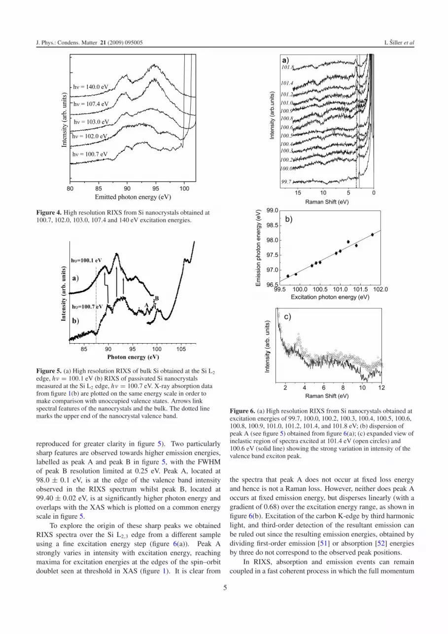
Figure 6. (a) High resolution RIXS from Si nanocrystals obtained atexcitation energies of 99.7, 100.0, 100.2, 100.3, 100.4, 100.5, 100.6,100.8, 100.9, 101.0, 101.2, 101.4, and 101.8 eV; (b) dispersion ofpeak A (see figure 5) obtained from figure 6(a); (c) expanded view ofinelastic region of spectra excited at 101.4 eV (open circles) and100.6 eV (solid line) showing the strong variation in intensity of thevalence band exciton peak.
the spectra that peak A does not occur at fixed loss energyand hence is not a Raman loss. However, neither does peak Aoccurs at fixed emission energy, but disperses linearly (with agradient of 0.68) over the excitation energy range, as shown infigure 6(b). Excitation of the carbon K-edge by third harmoniclight, and third-order detection of the resultant emission canbe ruled out since the resulting emission energies, obtained bydividing first-order emission [51] or absorption [52] energiesby three do not correspond to the observed peak positions.
In RIXS, absorption and emission events can remaincoupled in a fast coherent process in which the full momentum
5

J. Phys.: Condens. Matter 21 (2009) 095005 L Siller et al
is conserved even above threshold [53]. The energy shiftof peak A can then be rationalized in terms of dispersionof an electronic state within a crystalline system, providingfurther evidence for the crystallinity of the Si nanocrystal core.The intensity variation of peak A with excitation energy canbe understood if we attribute this feature to the formationof a valence exciton during the x-ray emission process. Asshown schematically in figure 2(c), the recombination of anelectron at the top of the valence band with a core hole canlead to the formation of a valence exciton final state with theelectron which had been promoted to the conduction bandduring photon absorption interacting with the valence bandhole. The influence of valence excitons on RIXS has beenconsidered theoretically by Minami and Nasu [54, 55] andby Shirley et al [53]. A strong intensity variation of valenceexciton features in RIXS can occur when the excitation energyis ‘on’ or ‘off’ resonance with the core exciton [53]. Whenthe energy of excitation is ‘on resonance’, the valence excitoncan have much a stronger intensity than the density of statesin the valence band due to efficient optical conversion fromthe core exciton to the valence exciton [53, 54], which agreeswell with the observed intensity variation of peak A comparedwith the valence band as emphasized in figure 6(c). Forcomparison in figure 6(a) we have put a dotted line at 3.4 eVto denote the X1–X4 valence exciton from bulk silicon; datafrom [53]. What is particularly striking about the valenceexciton in the nanocrystals is the energy range over which thepeak can be clearly observed, and its dispersion. Shin et al[56] observed a valence exciton feature in bulk Si at 18 Kdue to Raman scattering resonant with Si L2,3 core exciton,but this peak could be observed only within a very narrowexcitation energy window (99.30–99.99 eV) and appearedlocalized in energy. We suggest that the significantly widerenergy range over which the valence exciton can be observedin RIXS from the Si nanocrystals in figure 6(a) is due to theenhancement of core exciton formation at the x-ray absorptionedge observed in figure 1, which is in turn the result ofconfinement of the excited electron within the small volume ofthe nanocrystal. The dispersion observed for the nanocrystalvalence exciton feature over the Si L2,3 edge indicates thatdespite the formation of a core exciton as an intermediate state,momentum selectivity in the scattering process does not breakdown. Carlisle et al [57] have suggested that such retentionof momentum selectivity in the presence of a core excitonintermediate state arises from the projection of the intermediatestate onto a final state which is significantly less localized.
For peak B we did not have enough measurements todraw any significant conclusion because this peak is stronglysuperimposed on the intense elastic peak and hence notdetected. We speculate that peak B may arise from adefect or impurity state. The Si wafer from which thenanocrystals are produced is p-type doped with boron, butat such a low concentration (concentration between 1015 and1016 boron atoms per cm−3) that the majority of the resultingnanocrystals will not contain even a single dopant atom.Indeed, the concentration is such that it is unlikely that itwould be detected even in a measurement, such as that reportedhere, which averages over a macroscopic sample. It is,
however, possible that unintentional doping may occur duringnanocrystal production. Our previous work [8] has shown thatonly silicon, oxygen and carbon are present in the nanocrystalsamples, but it is possible that either the oxygen or carbon(which forms a relatively deep donor state, 0.25 eV below theconduction band minimum in bulk Si) may be present at lowconcentration within the Si nanocrystal core.
At an incident photon energy of 100.7 eV (L2 edge),figure 5(b), RIXS is most sensitive to Si–Si bonding, so datareflect the LPDOS of Si atoms in the core of the nanocrystals.When the LPDOS of the nanocrystals is compared with that ofbulk Si (also measured at the L2 edge for direct comparison—figure 5(a)), it is seen that features within the nanocrystalvalence band are as sharp and the total valence band widthis smaller (the dash dotted line in figure 3, shows the limitof the Si nanocrystal valence band). The narrower absorptionstructure in XES from the nanocrystal sample is not seen inbulk Si even at low temperature [56, 58]. In, addition, a lowenergy tail, peaking at ∼86.6 eV is observed in figure 5(b). Inbulk silicon, a similar feature was observed at ∼79 eV [59]due to multielectron transitions (‘shake up transitions’). Inthe case of Si nanocrystals this feature is shifted to higherphoton energy due to band narrowing—the valence band inthe nanocrystals extends only to ∼87.5 eV (dash dotted linein figure 5), a narrowing of ∼2 eV with respect to the bulk.We attribute the sharper bands in the XES of the nanocrystalsand the narrower overall valence band width, to quantumconfinement effects in the nanocrystals. The recently reportedXES work on silicon clusters in a SiO2 matrix reported byZimina et al [17], do not exhibit the multielectron excitationsor valence exciton peak (figure 5(b)). The absence of thesefeatures in the data reported in [17] may be due to thequenching of processes which occur in the core or on thesurface of the Si cluster by the SiO2 matrix in which theclusters are embedded.
The pronounced core excitonic features in x-ray absorp-tion and valence excitonic features in x-ray emission datamakes an accurate determination of band edges, and hencea band gap, extremely difficult. In order to explore thepossible effects of quantum confinement on the band gapof the nanocrystals we have collected x-ray excited opticalluminescence (XEOL) data for samples prepared by the sameprocedure [20, 21] as those used in the XAS and XESmeasurements. The XEOL data were obtained at roomtemperature (RT) and at 12 K, in order to reduce thermalbroadening. Figure 7 shows the emission spectrum of theSi nanocrystal film at RT, acquired with excitation energy of140 eV. Emission peak positions are found at 430 ± 10 nm(blue) and 620 ± 10 nm (orange) respectively, and it has beensuggested that these features originate from oxidized and non-oxidised Si, respectively [24]. In addition to these broad peaksa very sharp feature at 792 nm (1.56 eV), is observed with thesame excitation energy (see figure 7, inset), but only at lowtemperature (there is also possibly a small shoulder at 802 nm,but since the intensity of this feature is comparable to the noiselevel of the data it will not be discussed further). The sharpfeature at 792 nm is assigned to valence exciton recombinationin the Si nanocrystal. The presence of the excitonic feature
6

J. Phys.: Condens. Matter 21 (2009) 095005 L Siller et al
Figure 7. XEOL obtained at room temperature (main figure) and12 K (inset) with an excitation energy of 140 eV.
at low temperature, where thermal phonon population is lowsuggests that the band gap in the nanocrystals may be direct,in which case the energy of the excitonic peak provides aminimum value for the band gap of 1.56 eV—substantiallylarger than the (indirect) gap of bulk Si, 1.11 eV, so providingfurther evidence for quantum confinement.
In figure 8 the XOEL of SiNCs at 12 K taken withphoton energy of 150 eV is presented. Two narrow bandswith peak emission, at 594 nm (2.087 eV) and at 558 nm(2.222 eV), and with the full width at half maximum (FWHM)of 8 nm (28 meV) and 17 nm (68 meV), respectively, wereobserved. The maximum position of the bands correspond tothe theoretical values for the PL peaks of oxidized nanocrystalsof mean size ∼2 nm and ∼1.6 nm, respectively [60]. Thewidth of the both individual PL peaks is narrow giving thesize distribution of the nanocrystals to be ∼±0.1 nm [60].This is close to the previously reported mean radius values,2.2 ± 0.4 nm [21].
Although the room temperature PL data reported hereagree well with previously reported PL data excited with UVphotons (excitation energy 21.2 eV) [24], the position of theluminescence peaks and width at 12 K is different than in ourprevious report (in this work they are much narrower) [24].We believe that this is because in this work we have been verycareful not to expose the SiNCs to a high flux of the photons atany time in order to avoid possible bleaching effects.
4. Conclusions
In this work we have studied XAS, RIXS and XOEL fromalkyl-passivated silicon nanocrystals. Emission and absorptionspectra show a rich structure associated with electron–holeinteractions. The LPDOS measured by RIXS over the Siedge reveal that the LPDOS of the silicon core has discreteatomic-like states which are in agreement with recent PLstudies [35]. The overall valence band width is much narrower(by ∼2 eV) than for bulk silicon, which is in accordance withquantum confinement. The XAS data reveal that the edgeof the conduction band is masked by core exciton formationand this is why it was not possible to directly obtain the
Figure 8. XOEL obtained at 12 K with an excitation energy of150 eV.
band gap from XAS and XES data. However, with XOELdata we have determined that the band gap energy is notsmaller than 1.54 eV. The position and the narrowness ofthe photoluminescence bands in XOEL when compared withtheoretical predictions for oxidized Si nanocrystals [60] revealthat the nanocrystals have mean diameter of ∼2 and ∼1.6 nm,with ±0.1 nm spread in size. This is close to the previouslyreported mean diameter values of 2.2 ± 0.4 nm obtained fromSAXS, AFM, and STM [21].
Acknowledgments
LS is grateful to EPSRC and the EC ARI programme for afinancial support. AKC thanks EPSRC and the University ofNottingham for the award of a studentship. SK thanks theORS and the University of the Newcastle for a studentship.BRH and AH would like to thank EPSRC and CeNAMPSfor financial support. We thank Dr NRJ Poolton for helpfulcomments on the manuscript and for help in making the XOELmeasurements.
References
[1] Dhal J E, Liu S G and Carlson R M K 2003 Science 299 96[2] Willey T M, Bostedt C, van Buuren T, Dahl J E, Liu S G,
Carlson R M K, Terminello L J and Moller T 2005 Phys.Rev. Lett. 95 113401
[3] Wang Y, Kioupakis E, Lu X, Wegner D, Yamachika R,Dahl J E, Carlson R M K, Louie S G and Crommie M F2008 Nat. Mater. 7 38
[4] Canham L T 1990 Appl. Phys. Lett. 57 1046[5] Nash K J, Calcott P D J, Canham L T and Needs R J 1995
Phys. Rev. B 51 17698[6] Gole J L, Dudel F P, Grantier D and Dixon D A 1997 Phys.
Rev. B 56 2137[7] Marsen B, Lonfat M, Scheier P and Saltter K 2000 Phys. Rev. B
62 6892Sattler K 2002 Handbook of Thin Films Materials vol 5
Nanomaterials and Magnetic Thin Filmsed H S Nalwa (New York: Academic) and references therein
7

J. Phys.: Condens. Matter 21 (2009) 095005 L Siller et al
[8] Chao Y, Krishnamurthy S, Montalti M, Lie L H, Kjeldgaard L,Dhanak V R, Hunt M R C, Houlton A, Horrocks B R andSiller L 2005 J. Appl. Phys. 98 044316
[9] Hoffmann M A, Wrigge G, Issendorff P v, Muller J,Gartefor G and Haberland H 2001 Eur. Phys. J. D 16 9
[10] Eisebitt S, Luning J, Rubensson J-E and Eberhardt W 1999Phys. Status Solidi 215 803
[11] Kotani A and Shin S 2001 Rev. Mod. Phys. 73 203[12] Rubensson J-E 2000 J. Electron Spectrosc. 110 135[13] Eisebitt S, Luning J, Rubenson J-E, van Buuren T, Patitsas S N,
Tiedje T, Berger M, Arens-Fischer R, Frohnhoff S andEberhardt W 1996 Solid State Commun. 97 549
Eisebitt S, Luning J, Rubenson J-E, van Buuren T, Patitsas S N,Tiedje T, Berger M, Arens-Fischer R, Frohnhoff S andEberhardt W 1996 J. Electron Spectrosc. Relat. Phenom.79 135
[14] van Buuren T, Dinh L N, Chase L L, Siekhaus W J, Jimenez I,Terminello L J, Grush M, Callcott T A and Carlisle J A 1997Advances in microcrystalline and nanocrystallinesemiconductors Mater. Res. Soc. Symp. Proc. 171
van Buuren T, Dinh L N, Chase L L, Siekhaus W J andTerminello L J 1998 Phys. Rev. Lett. 80 3803
[15] Chang G S, Song J H, Chae K H, Whang C N, Kurmaev E Z,Shamin S N, Galakhov V R, Moewes A and Ederer D L2001 Appl. Phys. A 72 303
[16] Carlisle J A, Dongol M, Germanenko I N, Pithawalla Y B andEl-Shall M S 2000 Chem. Phys. Lett. 326 335
[17] Zimina A, Eisebitt S, Eberhardt W, Heitmann J andZacharias M 2006 Appl. Phys. Lett. 88 163103
[18] Gong X G 1995 Phys. Rev. B 52 14677[19] Katircioglu S and Erkoc S 2001 Physica E 9 314[20] Lie L H, Duerdin M, Tuite E M, Houlton A and Horrocks B R
2002 J. Electroanal. Chem. 538 183[21] Chao Y, Siller L, Krishnamurthy S, Kjeldgaard L, Patole S N,
Lie L H, O’Farrell N, Alsop T A, Houlton A andHorrocks B R 2007 Nat. Nanotechnol. 2 468
[22] Sham T K, Jiang D, Coulthard I, Lorimer J W, Feng X H,Tan K H, Frigo S P, Rosenberg R, Houghton D C andBryskiewich B 1993 Nature 363 332
[23] Naftel S J, Coulthard I and Antel W 2001 Appl. Phys. Lett.78 1847
[24] Chao Y, Yang J, Houlton A, Horrocks B R, Hunt M R C,Poolton N R J and Siller L 2006 Appl. Phys. Lett. 88 263119
[25] Bateman J E, Eagling R D, Horrocks B R and Houlton A 2000J. Phys. Chem. B 104 5557–65
[26] Sieval A B, van den Hout B, Zuilhof H and Sudholter E J R2001 Langmuir 17 2172
[27] Wallart X, de Villeneuve C H and Allongue P 2005 J. Am.Chem. Soc. 127 7871
[28] Nordgren J, Bay G, Cramm S, Nyholm R, Rubensson J-E andWassdahl N 1989 Rev. Sci. Instrum. 60 1690
[29] Kasrai M, Yin Z, Bancroft G M and Tan K H 1993 J. Vac. Sci.Technol. A 11 2694
[30] Hu Y F, Boukherroub R and Sham T K 2004 J. ElectronSpectrosc. Relat. Phenom. 135 143
[31] Bianconi A 1979 Surf. Sci. 89 41[32] Tanaka I, Kawai J and Adachi H 1995 Phys. Rev. B 52 11733[33] Wu Z Y, Jollet F and Seifert F 1998 J. Phys.: Condens. Matter
10 8083[34] Brown F C and Rustgi O P 1972 Phys. Rev. Lett. 28 497[35] Sychugov I, Juhasz R, Valenta J and Linnros J 2005 Phys. Rev.
Lett. 94 087405[36] Brown F C, Bachrach R Z and Skibowski M 1977 Phys. Rev. B
15 4781[37] Kane E O 1966 Phys. Rev. 146 558[38] Batson P E and Bruley J 1991 Phys. Rev. Lett. 67 350[39] Altarelli M and Dexter D L 1972 Phys. Rev. Lett. 29 1100[40] Suda Y, Obata K and Koshida N 1998 Phys. Rev. Lett. 80 3559[41] Lu Z, Lockwood D J and Baribeau J M 1995 Nature 378 258[42] Ma Y, Skytt P, Wassdahl N, Glans P, Mancini D C, Guo J and
Nordgren J 1993 Phys. Rev. Lett. 71 3725[43] Harada Y, Tokushima T, Takata Y, Takeuchi T, Kitajima Y,
Tanaka S, Kayanuma Y and Shin S 2004 Phys. Rev. Lett.93 017401
[44] Tanaka S and Kayanuma Y 1996 Solid State Commun. 100 77[45] Tanaka S and Kayanuma Y 2005 Phys. Rev. B 71 024302[46] Benisty H 1995 Phys. Rev. B 51 13281[47] Bockelmann U and Bastard G 1990 Phys. Rev. B 42 8947[48] Urayama J, Norris T B, Singh J and Bhattacharya P 2001
Phys. Rev. Lett. 86 4930[49] Wiech G, Feldhutter H O and Simunek A 1993 Phys. Rev. B
47 6981[50] Miyano K E, Ederer D L, Callcott T A, O’Brien W L, Jia J J,
Zhou L, Dong Q-Y, Ma Y, Woicik J C and Mueller D R1993 Phys. Rev. B 48 1918
[51] Carlisle J A, Shirley E L, Terminello L J, Jia J J, Callcott T A,Ederer D L, Perera R C C and Himpsel F J 1999 Phys. Rev.B 59 7433
[52] Diaz J, Anders S, Zhou X, Moler E J, Kellar S A andHussain Z 2001 Phys. Rev. B 64 125204
[53] Shirley E L, Soininen J A, Zhang G P, Carlisle J A,Callcott T A, Ederer D L, Terminello L J and Perera R C C2001 J. Electron Spectrosc. Relat. Phenom. 114–116 939
[54] Minami T and Nasu K 1998 J. Electron Spectrosc. Relat.Phenom. 92 231
[55] Minami T 1998 J. Phys. Soc. Japan 67 3958[56] Shin S, Agui A, Watanabe M, Fujisawa M, Tezuka W and
Ishii T 1996 Phys. Rev. B 53 15660[57] Carlisle J A, Blankenship S R, Terminello L J, Jia J J,
Callcott T A, Ederer D L, Perera R C C and Himpsel F J2000 J. Electron Spectrosc. Relat. Phenom. 110/111 323
[58] Eisebitt S, Luning J, Rubensson J E, Settels A, Dederichs P H,Eberhardt W, Patitsas S N and Tiedje T 1998 J. ElectronSpectrosc. Relat. Phenom. 93 245
[59] Livins P and Schnatterly S E 1988 Phys. Rev. B 37 6731[60] Wolkin M V, Jorne J, Fauchet P M, Allan G and
Delerue C 1999 Phys. Rev. Lett. 82 197
8


