Embed Size (px)
Citation preview

Journal of Alloys and Compounds 622 (2015) 243–249
Contents lists available at ScienceDirect
Journal of Alloys and Compounds
journal homepage: www.elsevier .com/locate / ja lcom
Design and electrical characterization of Au/Anthracene/p-Si/Al organic/inorganic heterojunction
http://dx.doi.org/10.1016/j.jallcom.2014.10.0600925-8388/� 2014 Elsevier B.V. All rights reserved.
⇑ Corresponding author. Tel.: +966 556669296; fax: +966 12 695 1449.E-mail address: [email protected] (A.A. Al-Ghamdi).
Attieh A. Al-Ghamdi a,⇑, Ahmed M. Nawar b, Farid El-Tantawy b, S.J. Yaghmour c, Ameer Azam a
a Center of Nanotechnology, King Abdulaziz University, Department of Physics, North Jeddah, Saudi Arabiab Department of Physics, Faculty of Science, Suez Canal University, Ismailia, Egyptc Department of Physics, King Abdulaziz University, North Jeddah, Saudi Arabia
a r t i c l e i n f o
Article history:Received 19 April 2014Accepted 10 October 2014Available online 20 October 2014
Keywords:AnthraceneRectification ratio (RR)Nanocrystalline structureCapacitance–voltagePhotovoltaic properties
a b s t r a c t
Hybrid organic/inorganic heterojunction of nanocrystalline Anthracene and p-Si was fabricated by usinga conventional thermal evaporation technique. The crystal and molecular structure of the Anthracenethin films were analyzed by means of X-ray diffraction (XRD), and Fourier Transformation-Infra Red(FT-IR) spectroscopy. The morphologies of the Anthracene/p-Si were investigated by scanning electronmicroscopy (SEM). The dark current–voltage (I–V) characteristics of Au/Anthracene/p-Si/Al heterojunc-tion were investigated at room temperature (293 K). The calculated series resistance and the shuntresistance of the device were found to be 440 X and 1.47 MX, respectively. The Cheung–Cheung andNorde’s models were used to investigate and determine the heterojunction parameters. The idealityfactor and barrier height values of the Au/Anthracene/p-Si/Al diode were obtained to be 1.1 and0.464 eV, respectively. The dependence of capacitance–voltage (C�2–V) for the device Anthracene/p-Siwas found to be almost linear. Essential junction parameters and performance of heterojunction estab-lished a photovoltaic behavior with an open circuit voltage (Voc) 0.382 V, short circuit photocurrent(ISC) 0.72 mA and power conversion efficiency (g) of 4.65%.
� 2014 Elsevier B.V. All rights reserved.
1. Introduction
Organic interfacial metal–semiconductor contacts have beenextensively investigated due to their potential use in a variety oforganic electronic and optoelectronic devices, such as field effecttransistors [1], organic light-emitting diodes (OLEDs) [2], photovol-taic (PV) cells [3,4] and photo detectors [5]. There are a number ofways to use organic molecules in the fabrication of electronic andoptoelectronic devices. Organic–inorganic (O/I) structure is one ofthem. Many authors have fabricated this kind of structures to ben-efit from advantages of both organic and inorganic materials in asingle device and modify electrical and photoelectrical propertiesof metal–semiconductor (MS) devices [6–16]. Schottky barrierheights of MS contacts can be manipulated by insertion of a dipolelayer between the semiconductor and the organic film. To date,many attempts have been made to realize a modification and acontinuous control of the barrier height by using a semiconductingorganic layer or an insulating layer [17].
Anthracene is an organic semiconductor with wide bandgap and was one of the first aromatic materials used in OLED
fabrication. Anthracene is a solid polycyclic aromatic hydrocarbonconsisting of three fused benzene rings. It is a component of coal-tar. Anthracene is a basic substance for production of anthraqui-none, dyes, pigments, insecticides, wood preservatives and coatingmaterials. The crystal structure of the anthracene is monoclinicwith large inter-planner spacing (d = 9.14 Å) and has a long rangecoherency with each (001) plane [18]. Due to the lowest surfaceenergy of (001) face, anthracene crystal grows by a periodiclayer-by-layer growth process along the (001) plane [19]. Efficientorganic light emitting diodes (OLEDs) were fabricated by using thinfilms of anthracene derivatives by Huang et al. [20] and Zhu et al.[21]. There is also a report on the use of anthracene based organicdye for the dye-sensitized solar cells [22]. P-type organic semicon-ductors, namely derivatives of pentacene, rubrene, anthracene orthiophene, have attracted great attention for their application inhigh-performance organic thin film transistors (OTFTs) [23,24].A new Anthracene-based X-shaped conjugated molecules havebeen used in high-performance (OTFT) fabrication (hole mobil-ity = 0.24 cm2 V�1 s�1) solely based on a solution process [25].Here, the present work aims to use Anthracene as received withoutany further purification, to fabricate Au/Anthracene/p-Si/Al hetero-junction and study the induced changes in the topological and thenanostructures of prepared Anthracene thin films and also to

244 A.A. Al-Ghamdi et al. / Journal of Alloys and Compounds 622 (2015) 243–249
estimate the related electronic parameter of the device before andafter annealing at temperature 373 K. The change in the annealingtime and different annealing temperatures have not consideredbecause they were not one of the objective of this study.
2. Experimental
To obtain an Au/Anthracene/p-Si/Al heterojunction, the device was prepared byusing a polished p-type Si wafer with (100) orientation and hole concentration of1.6 � 1023 m�3 with thickness of 400 lm. In order to remove the native oxide onp-Si surface, the substrate was etched by CP4 solution (HF:HNO3:CH3COOH in ratio1:6:1) for 10 s, then rinsed with deionized water and isopropyl alcohol and dried inan oven under Argon atmosphere. In order to configure the Si/Al structure, the ther-mal evaporation technique was used to fabricate the back contact of a relativelythick film of Al to the bottom of the p-Si substrate. Afterwards the p-Si/Al wasannealed in an oven of Argon-media at 823 K for 5 min. Thermal evaporation tech-nique (a high vacuum coating unit, Edward, E-306 A, England) was used to prepareAnthracene thin films with thickness 88 nm. The molecular structure of preparedthin films is shown in Fig. 1(a). A suitable quartz crucible heated slowly by a tung-sten coil was used for evaporating the Anthracene powder under a pressure ofabout 6 � 10�5 Pa. The Anthracene films were deposited onto p-Si/Al and well-cleaned glass substrates for structural and morphological studies. The substrateswere maintained at room temperature during deposition at a distance of 14 cmfrom the quartz crucible. The rate of deposition was controlled to be 1 nm/s usinga quartz crystal thickness monitor (Edwards, Model-FTM4). The first group wascharacterized as-grown. The second group was annealed (373 K) under roughingvacuum at 10�1 Pa with a soaking time of 1 h. Finally, gold metal was evaporatedby using tungsten coil on the masked Anthracene/p-Si/Al, in order to completethe structure of the aimed Au/Anthracene/p-Si/Al heterojunction on a form of ICchip as shown in Fig. 1(a).
2.1. Device fabrication of Au/Anthracene/p-Si/Al heterojunction
The fabricated Au/Anthracene/p-Si/Al heterojunctions were maintained on pre-cleaned glass substrates and were connected to commercial Pins for IC (integratedcircuits) by using very thin wires of copper and silver paste in order to avoid thescratches due to electrode connections and to have a stable device. The devices ofconfiguration Au/p-Si/Al can be tested by connected Pin1 and Pin3 to the measuringsystem. The common Pin1 is connected to the bottom Al-electrode and Pin3 is con-nected to the top electrode to get the behavior of Au/p-Si/Al. The common Pin1 isconnected to the bottom Al-electrode and Pin2 is connected to the top electrodeto get the behavior of Au/Anthracene/p-Si/Al (as shown in Fig. 1(b)).
2.2. Characterization
2.2.1. Structural characterizationThe structural characterization of Anthracene in powder, as-grown and
annealed thin films were performed using X-ray diffraction (XRD) system (modelX’-pert) using monochromatic Cu Ka radiation (k = 1.54056 Å) operated at 40 kVand 25 mA. The molecular structure of Anthracene in powder, as-grown andannealed thin films were investigated by using Fourier transform infrared (FT-IR)technique (Bruker, Vector 22) infrared spectrophotometer in the infrared spectralrange 400–4000 cm�1. The surface topography for as-grown and annealedAnthracene thin films was investigated by scanning electron microscopy (SEM)
Fig. 1. (a) Molecular structure Anthracene. (b) A
(Philips-XL30). A layer of gold of about 10 Å thickness was sputtered (S150A SputterCoater, Edward’s, England) on the as-grown and annealed Anthracene thin filmspecimens for SEM characterization.
2.2.2. Electrical characterizationThe dark current–voltage (I–V) characteristics of the fabricated devices were
measured simultaneously using a high impedance computerized electrometer(Keithley-6517B). The dark I–V characteristics were obtained in a complete darkchamber at room temperature or inside a dark furnace in case of measurementsat higher temperatures. The illuminated (I–V) characteristics were carried out byusing Keithley-6517B under different intensities (5–100 mW/cm2) of light providedby a halogen lamp. The intensity of the incident light was measured by using a dig-ital lux-meter (BCHA, model 93408). The dark capacitance–voltage (C–V) character-istics for the fabricated devices was measured at 1 MHz and at room temperature(293 K), using a computerized (C–V) HIOKI-bridge Model-3531.
3. Results and discussion
3.1. Structural investigation
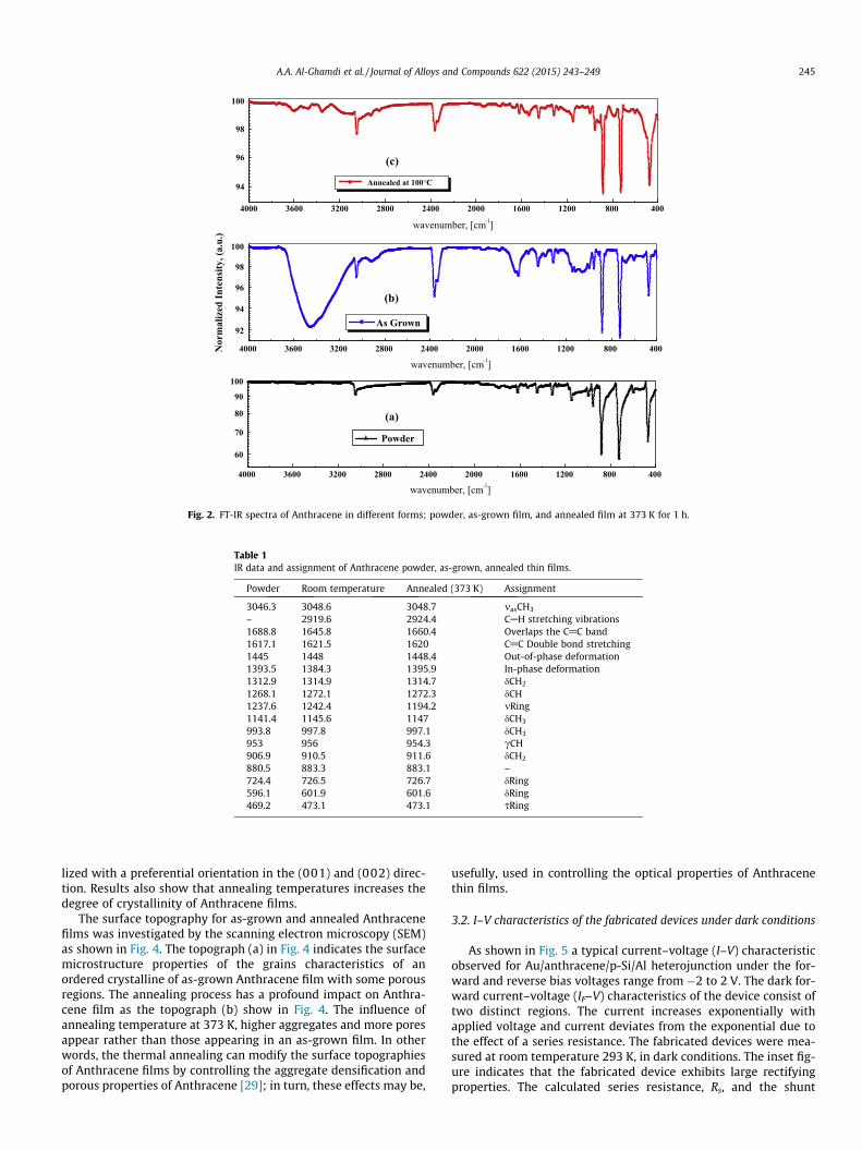
The chemical structure of the powder, the as-grown, and theannealed thin films were investigated by Fourier-transform infra-red (FT-IR) technique. The technique is based on the transmissionof infrared radiation and is sensitive to bulk changes in the rota-tional, bending and stretching vibrational modes of the moleculesin the material. FT-IR is an extremely useful technique to verify thecomposition of the film before and after processing steps [26].
Fig. 2 illustrates FT-IR spectra in the range 400–4000 cm�1
acquired from fresh Anthracene powder in comparison with spectracorresponding to the as-deposited and annealed thin films at 373 Kin air with soaking time of one hour (thickness 88 nm). Inspectionof this figure reveals that the spectrum of the as-deposited film doesnot change with evaporation indicating that the thermal evapora-tion technique is a good one to obtain undissociated and stoichiom-etric Anthracene films. In addition, the spectrum of the annealedfilm is also quite similar to that of the powder and the as-grownfilm, which revealed that Anthracene film has a thermal stabilityup to the used annealing temperature. The observed FT-IR bandsand their assignments are listed in Table 1, which are in a goodagreement with that available in literature [27].
Fig. 3 shows the X-ray diffraction patterns of Anthracene in theform of powder, as-grown and annealed thin films. Fig. 3(a) showsthe X-ray diffraction studies were conducted for anthracene com-mercial powder, Anthracene crystals revealed monoclinic unit cellwith a = 9.5 ÅA
0
, b = 6.0 ÅA0
, c = 8.5 ÅA0
, b = 103.61, and space group P21/c[26,27]. The lattice parameters evaluated by powder X-ray diffrac-tion studies of the grown anthracene are in good agreement withthe International Center for Diffraction Data (ICDD) values[26,28]. The patterns of diffractograms (b) and (c) in Fig. 3 indicatethat as-grown and annealed Anthracene films are partially crystal-
u/Anthracene/p-Si/Al hetrojunction device.
4000 3600 3200 2800 2400 2000 1600 1200 800 400
94
96
98
100
4000 3600 3200 2800 2400 2000 1600 1200 800 400
92
94
96
98
100
4000 3600 3200 2800 2400 2000 1600 1200 800 400
60
70
80
90
100
wavenumber, [cm-1]N
orm
aliz
ed In
tens
ity, (
a.u.
)
Powder
(a)
wavenumber, [cm-1]
wavenumber, [cm-1]
(c)
Annealed at 100 °C
As Grown
(b)
Fig. 2. FT-IR spectra of Anthracene in different forms; powder, as-grown film, and annealed film at 373 K for 1 h.
Table 1IR data and assignment of Anthracene powder, as-grown, annealed thin films.
Powder Room temperature Annealed (373 K) Assignment
3046.3 3048.6 3048.7 masCH3
– 2919.6 2924.4 CAH stretching vibrations1688.8 1645.8 1660.4 Overlaps the C@C band1617.1 1621.5 1620 C@C Double bond stretching1445 1448 1448.4 Out-of-phase deformation1393.5 1384.3 1395.9 In-phase deformation1312.9 1314.9 1314.7 dCH2
1268.1 1272.1 1272.3 dCH1237.6 1242.4 1194.2 mRing1141.4 1145.6 1147 dCH3
993.8 997.8 997.1 dCH3
953 956 954.3 cCH906.9 910.5 911.6 dCH2
880.5 883.3 883.1 –724.4 726.5 726.7 dRing596.1 601.9 601.6 dRing469.2 473.1 473.1 sRing
A.A. Al-Ghamdi et al. / Journal of Alloys and Compounds 622 (2015) 243–249 245
lized with a preferential orientation in the (001) and (002) direc-tion. Results also show that annealing temperatures increases thedegree of crystallinity of Anthracene films.
The surface topography for as-grown and annealed Anthracenefilms was investigated by the scanning electron microscopy (SEM)as shown in Fig. 4. The topograph (a) in Fig. 4 indicates the surfacemicrostructure properties of the grains characteristics of anordered crystalline of as-grown Anthracene film with some porousregions. The annealing process has a profound impact on Anthra-cene film as the topograph (b) show in Fig. 4. The influence ofannealing temperature at 373 K, higher aggregates and more poresappear rather than those appearing in an as-grown film. In otherwords, the thermal annealing can modify the surface topographiesof Anthracene films by controlling the aggregate densification andporous properties of Anthracene [29]; in turn, these effects may be,
usefully, used in controlling the optical properties of Anthracenethin films.
3.2. I–V characteristics of the fabricated devices under dark conditions
As shown in Fig. 5 a typical current–voltage (I–V) characteristicobserved for Au/anthracene/p-Si/Al heterojunction under the for-ward and reverse bias voltages range from �2 to 2 V. The dark for-ward current–voltage (IF–V) characteristics of the device consist oftwo distinct regions. The current increases exponentially withapplied voltage and current deviates from the exponential due tothe effect of a series resistance. The fabricated devices were mea-sured at room temperature 293 K, in dark conditions. The inset fig-ure indicates that the fabricated device exhibits large rectifyingproperties. The calculated series resistance, Rs, and the shunt

5 10 15 20 25 30 35 40 45 50 55 60
Nor
mal
ized
Inte
nsity
, (a.
u.)
2θθθ,,, ((degree))
(004
)
(001
)(0
01)
(002
)(0
02)
(003
)
(111
)(-2
02)(0
01)
Powder(a)
(002
)
Annealed at 373 K(c)
As Grown(b)
Fig. 3. X-ray diffraction patterns of Anthracene in the form of: (a) powder, (b) as-grown film and (c) annealed film at 373 K.
Fig. 4. (a) SEM micrograph of as-grown, (b) SEM micrograph of annealed Anthra-cene film.
-2.0 -1.5 -1.0 -0.5 0.0 0.5 1.0 1.5 2.0
10-7
10-6
10-5
10-4
10-3
I, (A
)
V , [Volt]
10-2
-2.0 -1.5 -1.0 -0.5 0.0 0.5 1.0 1.5 2.0
103
104
105
106
RSh
=1.47 MΩ
V , [Volt]
RS=440Ω
Rj=∂V/∂I
Fig. 5. Current–voltage (I–V) characteristics for Au/Anthracene/p-Si/Al at 293 K inforward and reverse conditions. The inset figure shows the junction resistancebehavior under forward and reverse voltage biasing conditions.
246 A.A. Al-Ghamdi et al. / Journal of Alloys and Compounds 622 (2015) 243–249
resistance, Rsh, are equal to 440 X and 1.47 MX respectively. Thedevice clearly exhibits the rectification behavior in dark, the calcu-lated rectification ratio, RR, is 881. The results show also the exis-tence of leakage current in reverse bias direction. The resultsexhibited diode-like behavior, which can be understood by the for-mation of a barrier at the interface.
The designed device structure behavior indicates the presenceof two conduction mechanisms which may be described by thetwo-lumped diode model as [30,31]:
I ¼ I01 expqðV � IRSÞ
n1kBT� 1
� �þ I02 exp
qðV � IRSÞn2kBT
� 1� �
þ V � IRS
RSh;
ð1Þ
where I0 is the reverse saturation current, q is the electronic charge,V is the applied voltage, kB is the Boltzmann constant, T is the tem-perature and n is the ideality factor, Rs and Rsh are series and shuntresistances, respectively. The current–voltage characteristics of thedevice are largely dependent on the series and shunt resistance. Alower value of Rs means that higher current will flow through thedevice. Rsh corresponds to fewer leaks in the device. The ideal devicewould have a series and parallel resistances approaching to zeroand infinity, respectively. The subscripts 1 and 2 indicate that twopossible contributions to the diode current could be present.
In the first region, the current I(v) through a SBD at a forwardbias (V), according to thermionic emission (TE) theory, is givenby the following relation [32,33]
IðvÞ ¼ I01 expqðV � IRSÞ
n1kBT
� �; ð2Þ
I01 ¼ AA�T2 exp � q;B
kBT
� �; ð3Þ
where A⁄ is Richardson constant (32 Acm�2 K�2 for p-Si), A is thearea of contact. In first region (V < 0.3 V), the exponential behaviorof I–V characteristics depends on the property of active materialused in the device under investigation. The slope of I–V characteris-tics in the exponential region depends on two parameters, i.e. ide-ality factor, n1 and the reverse saturation current I01. The idealityfactor gives information about the recombination process takingplace in the device and shape of the interfaces, i.e. the internal bulkmorphology for the organic devices [34]. The other parameter thataffects the exponential part of I–V characteristics is the saturationcurrent density which gives the number of charges able to over-come the energetic barrier in the reverse bias [35,36].
The values of /B and n = q/kT [1/(dln I/dV)] were determinedfrom the intercept and the slopes of the forward bias In I vs voltage(V) plot, respectively. The values of I01 obtained by extrapolatingthe linear intermediate bias-voltage region of the ln I–V curve tozero applied bias-voltage and the barrier height (BH) values calcu-lated from Eqs. (2) and (3). The calculated ideality factor for thediode in the first region is 1.1 and the investigated saturation cur-rent is 35 lA. the calculated barrier height of the fabricated Au/anthracene/p-Si/Al heterojunction is equal to 0.473 eV.
According to Cheung’s function, the series resistance, idealityfactor and the barrier height can be calculated at low biasing volt-age (V 6 0.4 V) [37]:

0.0 0.2 0.4 0.6 0.8 1.0 1.2 1.4 1.6 1.8 2.00.0
0.1
0.2
0.3
0.4
0.5
0.6
0.7
0.8
0.9
1.0
1.1
1.2
1.3
F(V)
V, [Volt]
F (V
)
φb=0.464 eVVMin=0.155 VoltF(VMin, IMin)=0.412 Volt
Fig. 7. The F(V) vs V plot of the Au/Anthracene/p-Si/Al at 293 K in dark.
A.A. Al-Ghamdi et al. / Journal of Alloys and Compounds 622 (2015) 243–249 247
dVdðln IÞ ¼ n
KTq
� �þ IRS; ð4Þ
and
HðIÞ ¼ V � nkTq
� �ln
1AA�T2
� �¼ IRS þ nub; ð5Þ
By using Eq. (5), the series resistance and ideality factor of thediode can be calculated from the slope and y-axis intercept ofthe dV/d(ln I) versus I plot as shown in Fig. 6. The values of seriesresistance and ideality factor were calculated to be 464 X and1.03 respectively. Also in the same Figure, by using Eq. (6); the plotof H(I) versus I will lead to a straight line with y-axis intercept tonub and the series resistance was obtained from the slope of thisstraight line. The calculated values of uB and RS were found to be0.456 eV and 463 X, respectively. It is worthy to note that the dif-ference in the barrier heights obtained from I(V) and H(I) methodscould be due to the fact that I–V characteristics uses the low volt-age region for calculation, while H(I) versus I plot is applied to thefull voltage range of forward bias characteristics of the diode[37,38].
Also, we used the Norde method to investigate the values of theseries resistance and the barrier height of the fabricated Au/anthra-cene/p-Si/Al heterojunction and Norde function can be expressedby the following relation [19,38]:
FðVÞ ¼ Vd� kT
qIðVÞ
AA�T2
� �; ð6Þ
where d is the integer (dimensionless), I(V) is the current obtainedfrom the I–V characteristics. The value of barrier height is calculatedafter getting minimum of the F vs V plot. Fig. 7 shows the F(V) vs Vplot of the device. The barrier height is given as [21,39]:
ub ¼ FðVoÞ þVo
d� kT
q; ð7Þ
where F(V0) is the minimum point of F(V) and Vmin is the corre-sponding voltage. The value of series resistance is also calculatedusing the formula [21,38]:
RS ¼kTðd� nÞ
qIo; ð8Þ
The values of barrier height and series resistance were deter-mined to be 0.464 eV and 472 kX, respectively by using then = 1.1. A small difference in values of series resistance obtained
6.0x10⁻⁵
1.2x10⁻⁴
1.8x10⁻⁴
2.4x10⁻⁴
3.0x10⁻⁴
3.6x10⁻⁴
4.2x10⁻⁴
4.8x10⁻⁴
0.0
0.1
0.2
0.3
0.4
0.5
0.6
0.7
0.8
0.9
1.0
Current , [A]
H (I)
dV/d
(lnI
)
0.0
0.1
0.2
0.3
0.4
0.5
0.6
0.7
0.8
0.9
1.0dV/d[lnI] vs. IH(I) vs I Fit Curve 1 Fit Curve 1
dV/d[lnI]=0.026+[464]*In=1.03RS=464Ω
H(I)=[463 ]*I-0.47Series Resistance=463 ΩBarrier Height= 0.456 eV
Fig. 6. Experimental dV/dln(I) and H(I) vs I plots of Au/Anthracene/p-Si/Al at 293 Kin dark.
from Cheung’s and Norde’s method is observed. This differencemay be due to the fact that Cheung’s model is applicable in thehigh-voltage region of the forward bias ln I–V characteristics, whileNorde’s model is applied to the full-voltage range of forward biasln I–V characteristics of the junctions [38].
3.3. C–V characteristics of the fabricated devices under dark conditions
The capacitance–voltage characteristics of Au/Anthracene/p-Si/Al heterojunction were investigated and measured under dark con-ditions, the junction capacitance was measured as a function ofreverse applied bias, Vappl, at 1 MHz. Measurement of the depletionregion capacitance under forward bias is difficult because thediode is conducting and the capacitance is shunted by a large con-ductance. However, the capacitance can be easily measured as afunction of the reverse bias. As the frequency increases, the inter-face capacitance contribution to the device capacitance decreases[39]. Fig. 8 shows the relation between 1/C2 vs. V of Au/Anthra-cene/p-Si/Al heterojunction at room temperature. The linearity ofthis relation indicates that the junction is considered as a one sidedabrupt heterojunction. This plot of the measured capacitance
-2.0 -1.5 -1.0 -0.5 0.0 0.5 1.0
0.2
0.4
0.6
0.8
1.0
1.2
1.4 1/C2–V characteristics
V, (volt)
1/ C
2 ( 10
21 F
-2)
Fig. 8. 1/C2–V characteristics for Anthracene/p-Si heterojunction.

0.00 0.05 0.10 0.15 0.20 0.25 0.30 0.35 0.40 0.45 0.50
0.1
0.2
0.3
0.4
0.5
0.6
0.7
0.8
0.9
1.0
V, (volt)
I, (m
A)
active area = π∗(0.2)2 cm2
I-V characteristics under an illumination (20 mW/cm2) for Anthracene /p-Si
FF=0.42
VOC=0.382 VI SC= 0.72 mA Pmax= 0.41 mA * 0.27 V
η=4.65 %
Fig. 9. I–V characteristics under an illumination (20 mW/cm2) for Anthracene/p-Si.
248 A.A. Al-Ghamdi et al. / Journal of Alloys and Compounds 622 (2015) 243–249
versus the applied reverse voltage shows the behavior for one-sided abrupt junctions. the relation between the junction capaci-tance, C, and the reverse applied potential for an abrupt junctioncan be given by the following equation:
C�2 ¼ 2ðVbi � VapplÞqeoeSiNaA2 ; ð9Þ
where Na is the Si doping density and Vbi and Vappl are the built-inand applied voltages, respectively. It is clear that C�2 increases lin-early by increasing the reverse applied voltage indicating that thejunction is a one-side abrupt junction. The carrier concentrationcan be estimated experimentally from the relation [39]:
dC�2
dV
!¼ 2
qeoeSiNaA2 ; ð10Þ
where dV/d(C�2) is the slope of the straight line and the interceptwith the horizontal asymptote gives the built-in potential, Vbi. Thecarrier concentration and the built-in potential were estimated tobe 0.2 � 1014 m�3 and 0.377 V, respectively. Fig. 9 shows the I–Vcharacteristics of Au/Anthracene/p-Si/Al under illumination. Thedevice of active area (0.124 cm2) exhibits a short-circuit current(ISC) of 0.72 mA, an open-circuit voltage (VOC) of 0.382 V. The fillfactor can be calculated as [39,40]
FF ¼ JmVm
JSCVOC; ð11Þ
where the product JmVm corresponds to the maximum power point.The calculated value of the FF = 42%. Then, the power conversionefficiency, g, is:
g ¼ JmVm
Po¼ JSCVOCFF
Po; ð12Þ
where Po is the incident light intensity �20 mW/cm2. These param-eters lead to power conversion efficiency (g) of 4.65%. Thisconversion efficiency is considered high comparable with CoM-TPP/p-Si solar cell (g = 3.6%) [41]. Dynamic I–V characteristicssupport the rectification and the photovoltaic performance andcharacterization of the investigated device under a dark andillumination condition.
4. Conclusions
We have successfully fabricated a Au/Anthracene/p-Si/Alorganic/inorganic heterojunction using thermal evaporation tech-nique. The Fabricated devices were characterized using varioustechniques. The calculated series resistance and the shunt resis-tance of the device were found to be 440 X and 1.47 MX, respec-tively. The Cheung–Cheung and Norde’s models were used toinvestigate and determine the heterojunction parameters. The ide-ality factor and barrier height values of the Au/Anthracene/p-Si/Aldiode were obtained to be 1.1 and 0.464 eV, respectively. Thedependence of capacitance–voltage (C�2–V) for the device Anthra-cene/p-Si was found to be almost linear which indicates that thejunction behavior is abrupt in nature. The performance of hetero-junction showed a photovoltaic behavior with an open circuitvoltage (Voc) 0.382 V, short circuit photocurrent (ISC) 0.72 mA andpower conversion efficiency (g) of 4.65%. This conversion efficiencyis considered high comparable with CoMTPP/p-Si solar cell(g = 3.6%) [41].
References
[1] Z. Bao, A.J. Lovinger, A. Dodabalapur, Appl. Phys. Lett. 69 (1996) 3066.[2] M. Ishii, Y. Taga, Appl. Phys. Lett. 80 (2002) 3430.[3] P. Peumans, S.R. Forrest, Appl. Phys. Lett. 79 (2001) 126.[4] S. Heutz, P. Sullivan, B.M. Sanderson, S.M. Schultes, T.S. Jones, Sol. Energy
Mater. Sol. Cells 83 (2004) 229.[5] P. Peumans, V. Bulovic, S.R. Forrest, Appl. Phys. Lett. 76 (2000) 3855.[6] A.R. Vearey-Roberts, D.A. Evans, Appl. Phys. Lett. 86 (2005) 072105.[7] O. Gullu, Microelectron. Eng. 87 (2010) 648.[8] A.A.M. Farag, E.A.A. El–Shazly, M. Abdel Rafea, A. Ibrahim, Sol. Energy Mater.
Sol. Cells 93 (2009) 853.[9] A.S. Kavasoglu, F. Yakuphanoglu, N. Kavasoglu, O. Pakma, O. Birgi, S. Oktik, J.
Alloy, Compounds 492 (2010) 421.[10] K. Akkılıc, Y.S. Ocak, S. Ilhan, T. Kılıcoglu, Synth. Met. 158 (2008) 969.[11] Y.S. Ocak, M. Kulakci, T. Kılıcoglu, R. Turan, K. Akkılıc, Synth. Met. 159 (2009)
1603.[12] R.K. Gupta, K. Ghosh, P.K. Kahol, Physica E 41 (2009) 1832.[13] Ö. Vural, Y. S�afak, S� Altındal, A. Türüt, Curr. Apl. Phys. 10 (2010) 761.[14] Tahsin Kılıcoglu, Yusuf Selim Ocak, Microelectron. Eng. 88 (2011) 150.[15] Murat Soylu, Fahrettin Yakuphanoglu, I.S. Yahia, Microelectron. Reliab. 52
(2012) 1355.[16] Z. Çaldıran, A.R. Deniz, S�. Aydogan, A. Yesildag, D. Ekinci, Superlattices
Microstruct. 56 (2013) 45.[17] O. Gullu, S. Aydogan, A. Turut, Microelectron. Eng. 85 (2008) 1647.[18] C.P. Brock, J.D. Dunity, Acta Crystallogr., Sect. B: Struct. Sci. 46 (1990) 795.[19] P. Zhang, J. Deng, X. Zeng, Z. Liu, Y. Qiu, H. Zhong, Y. Fan, J. Huang, J. Zhang, K.
Xub, J. Cryst. Growth 8 (2009) 470.[20] H. Huang, Q. Fu, S. Zhuang, G. Mu, L. Wang, J. Chen, D. Ma, C. Yang, Org.
Electron. 12 (2011) 1716.[21] M. Zhu, T. Ye, C.-G. Li, X. Cao, C. Zhong, D. Ma, J. Qin, C. Yang, J. Phys. Chem. C
115 (2011) 17965.[22] K.R.J. Thomas, P. Singh, A. Bahetia, Y.-C. Hsu, K.-C. Ho, J.T.s. Lin, Dyes Pigm. 91
(2011) 33.[23] G.R. Llorente, M.-B. D.-Madec, D.J. Crouch, R.G. Pritchard, S. Ogier, S.G. Yeates,
Chem. Commun. 35 (2009) 3059.[24] F. Cicoira, C. Santato, A. Dadvand, C. Harnagea, A. Pignolet, P. Bellutti, Z. Xiang,
F. Rosei, H. Meng, D.F. Perepichka, J. Mater. Chem. 18 (2008) 158.[25] Ki Hwa Jung, Suk Young Bae, Kyung Hwan Kim, Min Ju Cho, Kwangyeol Lee,
Zee Hwan Kim, Dong Hoon Choi, Dong Hoon Lee, Dae Sung Chung, Chan EonPark, Chem. Commun. 35 (2009) 5290–5292.
[26] K. Maex, M.R. Baklanov, D. Shamiryan, F. Lacopi, S.H. Brongersma, Z.S.Yanovitskaya, J. Appl. Phys. 93 (11) (2003) 8793.
[27] Irvine Huamin Hong, Ke Jie Tan, Minglin Toh, Hui Jiang, Keke Zhang, ChristianKloc, J. Cryst. Growth 363 (2013) 61.
[28] Nidhi Sinha, Manoj K. Gupta, Neeti Goel, Binay Kumar, Physica B 406 (2011)3206.
[29] M.M. El-Nahass, H.M. Abd El-Khalek, A.M. Nawar, Eur. Phys. J. Appl. Phys. 57(2012) 30201.
[30] A.S. Riad, Thin Solid Films 370 (2000) 253.[31] M.M. El-Nahass, A.A. Atta, E.F.M. El-Zaidia, A.A. Hendi, Microelectron. Eng. 116
(2014) 58.[32] S.M. Sze, Physics of Semiconductor Device, second ed., John Wiley & Sons, New
York, 1981.[33] E.H. Rhoderick, R.H. Williams, Metal-Semiconductor Contacts, second ed.,
Clarendon Press, Oxford, 1988.[34] M. Tucci, D. Caputo, J. Non-Cryst, Solids 338 (2004) 780.

A.A. Al-Ghamdi et al. / Journal of Alloys and Compounds 622 (2015) 243–249 249
[35] T. Kilicoglu, Thin Solid Films 516 (2008) 967.[36] B.K. Sharma, N. Khare, S. Ahmad, Solid State Commun. 149 (2009) 771.[37] S.K. Cheung, N.W. Cheung, Appl. Phys. Lett. 49 (1986) 85.[38] Ahmed A. Al-Ghamdi, Attieh A. Al-Ghamdi, Omar A. Al-Hartomy, Ahmed M.
Nawar, E. El-Gazzar, Farid El-Tantawy, F. Yakuphanoglu, J. Sol.-Gel. Sci.Technol. 10971 (2013) 3090.
[39] R.W. Wagner, J.S. Lindsey, J. Am. Chem. Soc. 116 (1994) 9759.[40] K. Tennakone, G.R.R. Kumara, I.R.M. Kottegoda, K.G.U. Wijayantha, V.P.S.
Perrera, J. Phys. D Appl. Phys. 31 (1998) 1492.[41] M.M. El-Nahass, M.A. Kamel, A.A. Atta, S.Y. Huthaily, Mater. Chem. Phys. 137
(2013) 716.


![Photochemical reaction of 9-nitro-substituted anthracene-like molecules 9-methyl-10-nitroanthracene and 12-methyl-7-nitrobenz[a]anthracene](https://img.pdfslide.net/doc/110x75/635694e6ea2708a6d301ab81/photochemical-reaction-of-9-nitro-substituted-anthracene-like-molecules-9-methyl-10-nitroanthracene.jpg)


