Embed Size (px)
Citation preview
Dynamic Analysis of a Boost Converter With Ripple Cancellation Network by Model-Reduction
Techniques Daniel Díaz, David Meneses, Jesús Ángel Oliver, Member, IEEE, Óscar García, Member, IEEE,
Pedro Alou, Member, IEEE, and José Antonio Cobos, Member, IEEE
Abstract—The boost topology with ripple cancellation network allows input and output current ripples attenuation, which means the suppression of the input filter and a high reduction of the output filter. However, to achieve the ripple cancellation, the com-plexity and the number of components of the converter need to be increased as compared with the conventional boost. A detailed analysis is developed to specify the advantages and disadvantages of this topology. This paper presents the averaged model that derives the complex transfer function of the topology. The theoretical transfer function is obtained. Due to the complexity of the seventh-order transfer function that is obtained, a simplified second-order transfer function is calculated to simplify control design calcula-tions. A comparison between the analyzed topology and a conventional boost in terms of weight and losses is carried out. To estímate the current ripple calculation, it is proposed to use the ripple theorem, which allows an estimation of the efficiency of the cancellation network using the averaged model. A prototype to valídate ripple cancellation and the dynamic analysis is developed. Measured waveforms and Bode plots are enclosed. Current ripple cancellation at the input and output in both conduction modes of the converter is also validated.
Index Terms—Boost converter, dynamic analysis, ripple cancellation, ripple theorem, two inductors.
I. INTRODUCTION
IN the design of a converter for a space application, weight, volume, and efficiency are critical design parameters. Sev-
eral boost-derived topologies have been considered for a particular space application: classical boost, interleaved boost, two-inductor boost [1], boost with ripple cancellation network [2], and boost with switch near ground [3], [4]. A comparison re-garding power losses, bandwidth, weight, and volume between the five candidate topologies is conducted in [5]. This comparison shows that the boost converter with ripple cancellation network has several advantages over the classical boost converter for the considered application. This topology is analyzed in detail in this paper and further comparison with a classical boost converter is presented.
A necessary element for the correct operation of the system is the filter, both at the input and the output. These two elements
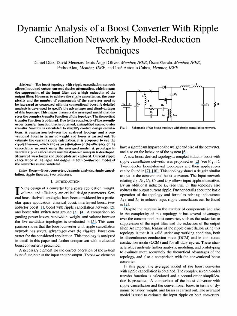
Fig. 1. Schematic of the boost topology with ripple cancellation network.
have a significant impact on the weight and size of the converter, and also on the behavior of the system [6].
A new boost-derived topology, a coupled inductor boost with ripple cancellation network, was proposed in [2] (see Fig. 1). Two-inductor boost-derived topologies and their applications can be found in [7]-[10]. This topology shows a de gain similar to that in the conventional boost converter. The input network relating £ 2 , ^ 1 , 6 2 , 6 3 , and L i e allows input ripple attenuation. By an additional inductor L 3 (see Fig. 1), this topology also reduces the output current ripple. Further details about the basic operation of the topology and formulas relating inductances L I A and L2 to achieve input ripple cancellation can be found in[2] .
Despite the increase in the number of components and also in the complexity of this topology, it has several advantages over the conventional boost converter, such as the reduction or suppression of the input filter and the reduction of the output filter. An important feature of the ripple cancellation using this topology is that it is valid under any working condition, both in discontinuous conduction mode (DCM) and in continuous conduction mode (CCM) and for all duty eyeles. These char-acteristics motivate further analysis, modeling, and prototyping to evalúate more accurately the theoretical advantages of the topology, and also a comparison with the conventional boost converter.
In this paper, the averaged model of the boost converter with ripple cancellation is obtained. The complex seventh-order transfer function is calculated and a second-order simplifica-tion is presented. A comparison of the boost converter with ripple cancellation and the conventional boost in terms of dynamic behavior, weight, and losses is carried out. The averaged model is used to estimate the input ripple on both converters.
(1-d)(<ig(t)>-<iL2(t)>)
3n¡rpíi^^ (nc/nA)(-<ÍL2(t)>)-(nB/nA)<iJ1B(t)>
^ C 5 ^ R <¡L1B(t)>
(nB/nA)<VL1A(t)>
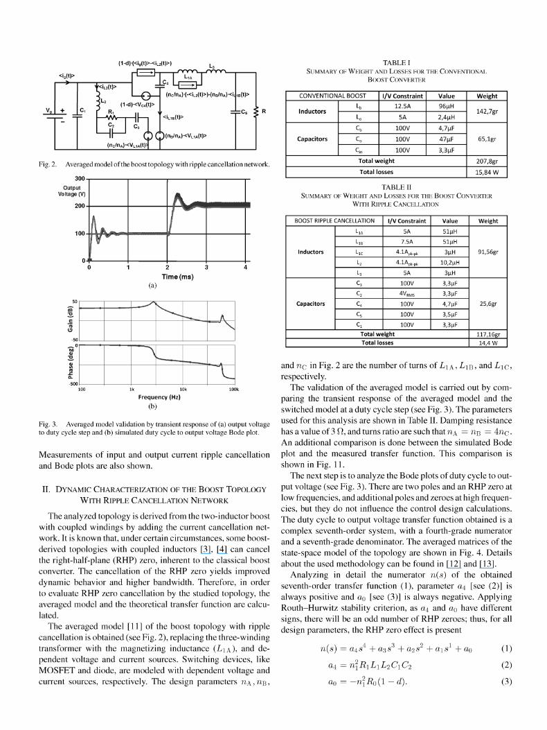
Fig. 2. Averaged model of the boost topology with ripple cancellation network.
300
Output Voltage (V)
200
100 JL~-j a
(a)
2 3
Time(ms)
•N _^o
Frequency (Hz)
(b)
Fig. 3. Averaged model validation by transient response of (a) output voltage to duty cycle step and (b) simulated duty cycle to output voltage Bode plot.
Measurements of input and output current ripple cancellation and Bode plots are also shown.
II. DYNAMIC CHARACTERIZATION OF THE BOOST TOPOLOGY
WITH RIPPLE CANCELLATION NETWORK
The analyzed topology is derived from the two-inductor boost with coupled windings by adding the current cancellation network. It is known that, under certain circumstances, some boost-derived topologies with coupled inductors [3], [4] can cancel the right-half-plane (RHP) zero, inherent to the classical boost converter. The cancellation of the RHP zero yields improved dynamic behavior and higher bandwidth. Therefore, in order to evalúate RHP zero cancellation by the studied topology, the averaged model and the theoretical transfer function are calcu-lated.
The averaged model [11] of the boost topology with ripple cancellation is obtained (see Fig. 2), replacing the three-winding transformer with the magnetizing inductance (LIA) , and de-pendent voltage and current sources. Switching devices, like MOSFET and diode, are modeled with dependent voltage and current sources, respectively. The design parameters TÍA, TÍB ,
TABLEI SUMMARY OF WEIGHT AND LOSSES FOR THE CONVENTIONAL
BOOST CONVERTER
CONVENTIONAL BOOST
Inductors
Capacitors
Lb
Lo
cb
Q Qn
l/V Constraint
12.5A
5A
100V
100V
100V
Valué
96|iH
2,4|iH
4,7|iF
47|iF
3,3uJ=
Total weight
Total losses
Weight
142,7gr
65, lgr
207,8gr
15,84 W
TABLE II SUMMARY OF WEIGHT AND LOSSES FOR THE BOOST CONVERTER
WITH RIPPLE CANCELLATION
BOOST RIPPLE CANCELLATION
Inductors
Capacitors
LIA
LIB
Lie
L2
L3
c3
c2
c4
c5
Ci
l/V Constraint
5A
7.5A
4-lApk.pk
4-lApk.pk
5A
100V
4VRMS
100V
100V
100V
Valué
51uH
51|iH
3|iH
10,2uH
3|iH
3,3uF
3,3uF
4,7|iF
3,5uF
3,3uF
Total weight
Total losses
Weight |
91,56gr
25,6gr
H7,16gr
14,4 W |
and TIQ in Fig. 2 are the number of turns of L\A , LIB > and L\Q , respectively.
The validation of the averaged model is carried out by com-paring the transient response of the averaged model and the switched model at a duty cycle step (see Fig. 3). The parameters used for this analysis are shown in Table II. Damping resistance has a valué of 3 Q, and turns ratio are such that n\ = riB = 4nc. An additional comparison is done between the simulated Bode plot and the measured transfer function. This comparison is shown in Fig. 11.
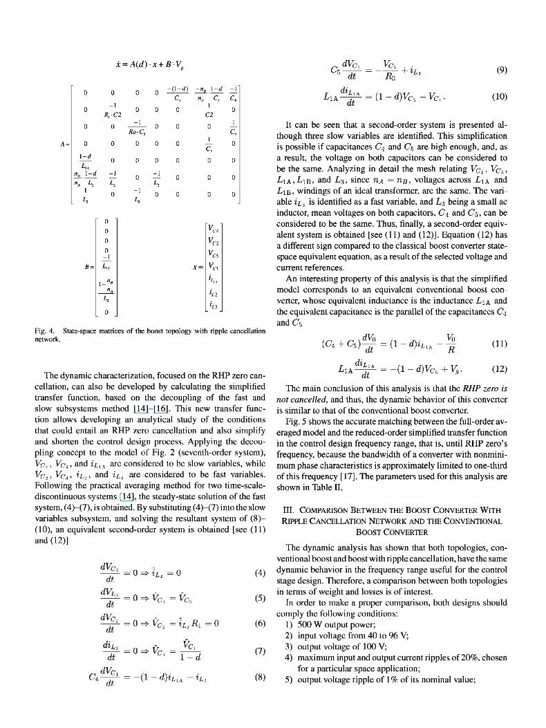
The next step is to analyze the Bode plots of duty cycle to output voltage (see Fig. 3). There are two poles and an RHP zero at low frequencies, and additional poles and zeroes at high frequen-cies, but they do not influence the control design calculations. The duty cycle to output voltage transfer function obtained is a complex seventh-order system, with a fourth-grade numerator and a seventh-grade denominator. The averaged matrices of the state-space model of the topology are shown in Fig. 4. Details about the used methodology can be found in [12] and [13].
Analyzing in detail the numerator n(s) of the obtained seventh-order transfer function (1), parameter a^ [see (2)] is always positive and ao [see (3)] is always negative. Applying Routh-Hurwitz stability criterion, as a^ and ao have different signs, there will be an odd number of RHP zeroes; thus, for all design parameters, the RHP zero effect is present
n(s) = a^s + a^s'
ao = — ni .ño (1 — d).
a2s2 + ais1 + a 0 (1)
(2)
(3)
0
0
0
0
\-d
u 1
B =
x = A(d)
0 0
RXC2
0
0
0
- 1
0
0
0
0
0 - 1
A7
nA
u 0
- 1 RoC5
0
0
0
- 1
x + BVg
0 ^ ^
0 0
0 0
0 0
0 0
± o L2
0 0
-nB \-d
nA C4
1 C2
0
1
0
0
0
x =
XA V V C 2
VC5
' A ,
lL2
lL3
- 1
0
i
c5
0
0
0
0
Fig. 4. State-space matrices of the boost topology with ripple cancellation network.
The dynamic characterization, focused on the RHP zero cancellation, can also be developed by calculating the simplified transfer function, based on the decoupling of the fast and slow subsystems method [14]—[16]. This new transfer function allows developing an analytical study of the conditions that could entail an RHP zero cancellation and also simplify and shorten the control design process. Applying the decoupling concept to the model of Fig. 2 (seventh-order system), ^c4 ? Vc5 •> and %LIK are considered to be slow variables, while ^c2 > Vc3' ^ 2 ' a nd ¿L3
a r e considered to be fast variables. Following the practical averaging method for two time-scale-discontinuous systems [14], the steady-state solution of the fast system, (4)-(7), is obtained. By substituting (4)-(7) into the slow variables subsystem, and solving the resultant system of (8)-(10), an equivalent second-order system is obtained [see (11) and (12)]
dVCz
dt 0 => iL2 = 0
dVr
a
dt
dVc2
dt
diL2
~dT dVc,
[ dt
^=0^VC,= VCb
0^VC2 =¡L2RI = 0
O^Vct 1-d
-(l-d)iLlA -iL:i
(4)
(5)
(6)
(7)
(8)
G
LIA
dVCí
dt lu
^ = V-Wc.-va.
(9)
(10)
It can be seen that a second-order system is presented al-though three slow variables are identified. This simplification is possible if capacitances C± and C$ are high enough, and, as a result, the voltage on both capacitors can be considered to be the same. Analyzing in detail the mesh relating Vc4, Vc5, £ I A , £ I B > and L3, since UA =UB, voltages across LIA and L I B , windings of an ideal transformer, are the same. The variable ii3 is identified as a fast variable, and L3 being a small ac inductor, mean voltages on both capacitors, C4 and C5, can be considered to be the same. Thus, finally, a second-order equivalent system is obtained [see (11) and (12)]. Equation (12) has a different sign compared to the classical boost converter state-space equivalent equation, as a result of the selected voltage and current references.
An interesting property of this analysis is that the simplified model corresponds to an equivalent conventional boost converter, whose equivalent inductance is the inductance LIA and the equivalent capacitance is the parallel of the capacitances C4 and C5
(CA + c5)^ = (i-d)iLlA-^ ( i i )
L 1A-
dt diLíA
dt
R
-(i-d)Vc5+vg. (12)
The main conclusión of this analysis is that the RHP zero is not cancelled, and thus, the dynamic behavior of this converter is similar to that of the conventional boost converter.
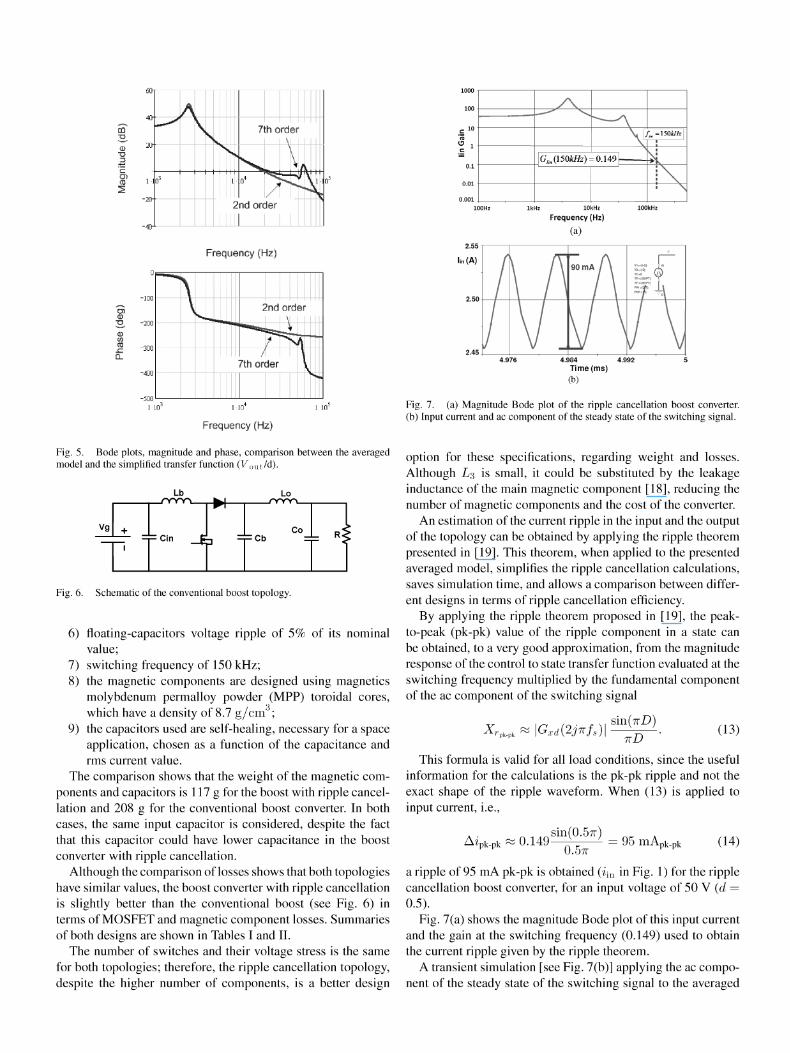
Fig. 5 shows the accurate matching between the full-order av-eraged model and the reduced-order simplified transfer function in the control design frequency range, that is, until RHP zero's frequency, because the bandwidth of a converter with nonmini-mum phase characteristics is approximately limited to one-third of this frequency [17]. The parameters used for this analysis are shown in Table II.
III. COMPARISON BETWEEN THE BOOST CONVERTER WITH
RIPPLE CANCELLATION NETWORK AND THE CONVENTIONAL
BOOST CONVERTER
The dynamic analysis has shown that both topologies, conventional boost and boost with ripple cancellation, have the same dynamic behavior in the frequency range useful for the control stage design. Therefore, a comparison between both topologies in terms of weight and losses is of interest.
In order to make a proper comparison, both designs should comply the following conditions:
1) 500 W output power; 2) input voltage from 40 to 96 V; 3) output voltage of 100 V; 4) máximum input and output current ripples of 20%, chosen
for a particular space application; 5) output voltage ripple of 1% of its nominal valué;
Di
60-
1-
40-
o3
JJJ
7th order i \i
\ r̂ 2nd order
u L
A 1 •jo
Frequency (Hz)
u
-vin
] :
r̂ 7thor
>nd
r ;Jer
Of
\ 1 -
d
^
sr
Frequency (Hz)
Fig. 5. Bode plots, magnitude and phase, comparison between the averaged model and the simplified transfer function (Vout/d).
Lb
vg ^ C i n C-, ^ C b d=
Lo
Co
Fig. 6. Schematic of the conventional boost topology.
6) floating-capacitors voltage ripple of 5% of its nominal valué;
7) switching frequency of 150 kHz; 8) the magnetic components are designed using magnetics
molybdenum permalloy powder (MPP) toroidal cores, which have a density of 8.7 g/cm ;
9) the capacitors used are self-healing, necessary for a space application, chosen as a function of the capacitance and rms current valué.
The comparison shows that the weight of the magnetic components and capacitors is 117 g for the boost with ripple cancel-lation and 208 g for the conventional boost converter. In both cases, the same input capacitor is considered, despite the fact that this capacitor could have lower capacitance in the boost converter with ripple cancellation.
Although the comparison of losses shows that both topologies have similar valúes, the boost converter with ripple cancellation is slightly better than the conventional boost (see Fig. 6) in terms of MOSFET and magnetic component losses. Summaries of both designs are shown in Tables I and II.
The number of switches and their voltage stress is the same for both topologies; therefore, the ripple cancellation topology, despite the higher number of components, is a better design
1000
100
c l u
» 1
0.001
V /M=150Jfc//z|
\Grm(l50kHz) = 0.1491 ^ ¡
\^ • \
1kHz 10kHz
Frequency (Hz)
(a)
Fig. 7. (a) Magnitude Bode plot of the ripple cancellation boost converter, (b) Input current and ac component of the steady state of the switching signal.
option for these specifications, regarding weight and losses. Although L3 is small, it could be substituted by the leakage inductance of the main magnetic component [18], reducing the number of magnetic components and the cost of the converter.
An estimation of the current ripple in the input and the output of the topology can be obtained by applying the ripple theorem presented in [19]. This theorem, when applied to the presented averaged model, simplifies the ripple cancellation calculations, saves simulation time, and allows a comparison between differ-ent designs in terms of ripple cancellation efficiency.
By applying the ripple theorem proposed in [19], the peak-to-peak (pk-pk) valué of the ripple component in a state can be obtained, to a very good approximation, from the magnitude response of the control to state transfer function evaluated at the switching frequency multiplied by the fundamental component of the ac component of the switching signal
Xrv] \Gxd(2J7Tfs)\ sin(7r,D)
7VD (13)
This formula is valid for all load conditions, since the useful information for the calculations is the pk-pk ripple and not the exact shape of the ripple waveform. When (13) is applied to input current, Le.,
Ai ̂pk-pk : 0.149 sin(0.57r)
0.57T 95 mApk.pk (14)
a ripple of 95 mA pk-pk is obtained (i[n in Fig. 1) for the ripple cancellation boost converter, for an input voltage of 50 V (d = 0.5).
Fig. 7(a) shows the magnitude Bode plot of this input current and the gain at the switching frequency (0.149) used to obtain the current ripple given by the ripple theorem.
A transient simulation [see Fig. 7(b)] applying the ac component of the steady state of the switching signal to the averaged
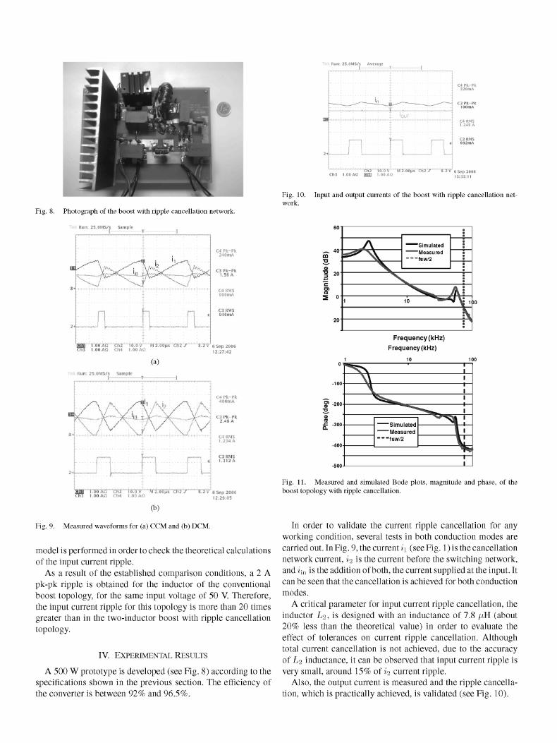
Fig. 8. Photograph of the boost with ripple cancellation network.
Run: 25.0MS/'s Sample
(a) Run: 25.OMS/S sample
| r.
Wa 'l.QO'Sñ CF2 i 0.0 V M2.00jiS Ch2 J S.2 V 6 5<?D 2006 Ol3 I.0GAÍ3 Ch4 100 AQ 12 29 05
(b)
Fig. 9. Measured waveforms for (a) CCM and (b) DCM.
model is performed in order to check the theoretical calculations of the input current ripple.
As a result of the established comparison conditions, a 2 A pk-pk ripple is obtained for the inductor of the conventional boost topology, for the same input voltage of 50 V. Therefore, the input current ripple for this topology is more than 20 times greater than in the two-inductor boost with ripple cancellation topology.
IV. EXPERIMENTAL RESULTS
A 500 W prototype is developed (see Fig. 8) according to the speciflcations shown in the previous section. The efflciency of the converter is between 92% and 96.5%.
¡:
f 1 | 1 «.
L í L
C4 Pk-Pk 320mA
C3 Pk-Pk lOOmA
C4 RMS 1.248 A
C3RMS 692mA
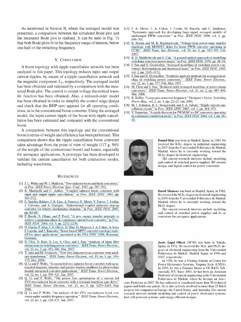
Fig. 10. work.
Input and output currents of the boost with ripple cancellation net-
Frequency(kHz)
Frequency(kHz)
o-
-500-
" ^ \ í
Simulated ^Measu red
fsw/2
1
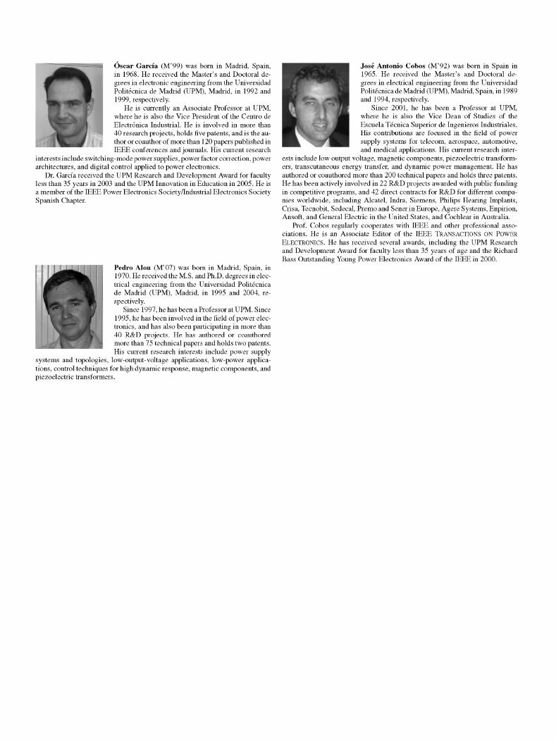
Fig. 11. Measured and simulated Bode plots, magnitude and phase, of the boost topology with ripple cancellation.
In order to validate the current ripple cancellation for any working condition, several tests in both conduction modes are carriedout. In Fig. 9, the current «i (see Fig. 1) is the cancellation network current, n is the current before the switching network, and «in is the addition of both, the current supplied at the input. It can be seen that the cancellation is achieved for both conduction modes.
A critical parameter for input current ripple cancellation, the inductor L2, is designed with an inductance of 7.8 ,«H (about 20% less than the theoretical valué) in order to evalúate the effect of tolerances on current ripple cancellation. Although total current cancellation is not achieved, due to the accuracy of L2 inductance, it can be observed that input current ripple is very small, around 15% of n current ripple.
Also, the output current is measured and the ripple cancellation, which is practically achieved, is validated (see Fig. 10).
As mentioned in Section II, where the averaged model was presented, a comparison between the simulated Bode plot and the measured Bode plot is realized. It can be seen in Fig. 11 that both Bode plots fit in the frequency range of interest, below one-half of the switching frequency.
V. CONCLUSIÓN
A boost topology with ripple cancellation network has been analyzed in this paper. This topology reduces input and output current ripples, by means of a ripple cancellation network and the magnetic component L-¿, respectively. The averaged model has been obtained and validated by a comparison with the measured Bode plot. The control to output voltage theoretical transfer function has been obtained. Also, a reduced-order model has been obtained in order to simplify the control stage design and check that the RHP zero appears for all operating condi-tions, as in the conventional boost converter. Using the averaged model, the input current ripple of the boost with ripple cancellation has been estimated and compared with the conventional boost.
A comparison between this topology and the conventional boost in terms of weight and efficiency has been performed. This comparison shows that the ripple cancellation boost converter takes advantage from the point of view of weight (117 g, 56% of the weight of the conventional boost) and losses, especially for aerospace applications. A prototype has been developed to validate the current cancellation for both conduction modes, including waveforms.
REFERENCES
[1] J. L. White and W. J. Muldoon, "Two-inductor boost and buck converters," in Proc. IEEE Power Electron. Spec. Conf., 1987, pp. 387-392.
[2] R. Martinelli and C. Ashley, "Coupled inductor boost converter with input and output ripple cancellation," in Proc. IEEE APEC 1991, pp. 567-572.
[3] E. Sanchis-Kilders, J. B. Ejea, A. Ferreres, E. Maset, V. Esteve, J. Jordán, J. Cálvente, and A. Garrigós, "Bidirectional coupled inductors step-up converter for battery discharging-charging," in Proc. IEEE PESC 2005, pp. 64-68.
[4] R Rueda, S. Ghani, and P. Perol, "A new energy transfer principie to achieve a mínimum phase & continuous current boost converter," in Proc. IEEE PESC 2004, vol. 3, pp. 2232-2236.
[5] O. García, P Alou, J. A. Oliver, D. Díaz, D. Meneses, J. A. Cobos, A. Soto, E Lapeña, and J. Rancaño, "Boost-based MPPT converter topology trade-off for space applications," presented at the ESA ESPC 2008, Konstanz, Germany.
[6] B. Choi, D. Kim, D. Lee, S. Choi, and J. Sun, "Analysis of input filter interactions in switching power converters," IEEE Trans. Power Electron., vol. 22, no. 2, pp. 452-460, Mar. 2007.
[7] Y. Jang and M. Jovanovic, "New two-inductor boost converter with auxil-iary transformer," IEEE Trans. Power Electron., vol. 19, no. 1, pp. 169-175, Dec. 2004.
[8] Q. Li and P Wolfs, "A current fed two-inductor boost converter with an in-tegrated magnetic structure and passive lossless snubbers for photovoltaic module integrated converter applications," IEEE Trans. Power Electron., vol. 22, no. 1, pp. 309-321, Jan. 2007.
[9] Q. Li and R Wolfs, "The power loss optimization of a current fed ZVS two-inductor boost converter with a resonant transition gate drive," IEEE Trans. Power Electron., vol. 21, no. 5, pp. 1253-1263, Sep. 2006.
[10] Q. Li and P Wolfs, "An analysis of the ZVS two-inductor boost converter under variable frequency operation," IEEE Trans. Power Electron., vol. 22, no. 1, pp. 120-131, Jan. 2007.
[11] J. A. Oliver, J. A. Cobos, J. Uceda, M. Rascón, and C. Quiñones, "Systematic approach for developing large-signal averaged models of multioutput PWM converters," in Proc. IEEE PESC 2000, vol. 2, pp. 696-701.
[12] B. Bryant and M. K. Kazimierczuk, "Voltage-loop power-stage transfer functions with MOSFET delay for boost PWM converter operating in CCM," IEEE Trans. Ind. Electron., vol. 54, no. 1, pp. 347-353, Feb. 2007.
[13] R. D. Middlebrook and S. Cuk, "A general unified approach to modelling switching-converter power stages,"in Proc. IEEE PESC 1976, pp. 18-34.
[14] J. Sun and H. Grotstollen, "Averaged modelling of switching power converters: Reformulation and theoretical basis," in Proc. IEEE PESC 1992, vol. 2, pp. 1165-1172.
[15] J. Sun and H. Grotstollen, "Symbolic analysis methods for averaged modeling of switching power converters," IEEE Trans. Power Electron., vol. 12, no. 3, pp. 537-546, May 1997.
[16] M. Chen and J. Sun, "Reduced-order averaged modeling of active-clamp converters," IEEE Trans. Power Electron., vol. 21, no. 2, pp. 487-494, Mar. 2006.
[17] R. Ridley, "Loop gain crossover frequency," Designer's Series, Switching Power Mag., vol. 2, no. 1, pp. 22-25, Jan. 2001.
[18] M. J. Schutten, R. L. Steigerwald, and J. A. Sabaté, "Ripple current cancellation circuit," in Proc. IEEE APEC 2003, vol. 1, pp. 464-470.
[19] V Vorperian, "A ripple theorem for PWM DC-to-DC converters operating in continuous conduction mode," in Proc. IEEE PESC 2004, vol. 1, pp. 28-35.
Daniel Díaz was born in Madrid, Spain, in 1980. He received the B.Sc. degree in industrial engineering in 2007 from the Universidad Politécnica de Madrid, Madrid, where he is currently working toward the M.Sc. degree in electrical engineering.
His current research interests include modeling and control of switched power supplies, RF circuits design, and digital control for power converters.
David Meneses was born in Madrid, Spain, in 1982. He received the M.Sc. degree in electrical engineering in 2009 from the Universidad Politécnica de Madrid, Madrid, where he is currently working toward the Ph.D. degree.
His current research interests include modeling and control of switched power supplies and dc-ac converters for aerospace applications.
Jesús Ángel Oliver (M'00) was born in Toledo, Spain, in 1972. He received the M.S. and Ph.D. de-grees in electrical engineering from the Universidad Politécnica de Madrid, Madrid, Spain, in 1996 and 2007, respectively.
In 1996, he was a Visiting Scholar at Center for Power Electronics Systems, Virginia Tech. (CPES). In 2000, he was a Summer Intern at GE R&D, Sch-enectady, NY. Since 2001, he has been an Assistant Professor of electrical engineering at the Universidad Politécnica de Madrid, where he became an Asso-
ciate Professor in 2007. He has authored or coauthored more than 50 technical papers and holds one patent. He is also actively involved in more than 25 R&D projects for companies in Europe, the United States, and Australia. His current research interests include modeling and control of power electronics systems, fuel-cell-powered systems, and energy-efficient designs.
Óscar García (M'99) was born in Madrid, Spain, in 1968. He received the Master's and Doctoral de-grees in electronic engineering from the Universidad Politécnica de Madrid (UPM), Madrid, in 1992 and 1999, respectively.
He is currently an Associate Professor at UPM, where he is also the Vice President of the Centro de Electrónica Industrial. He is involved in more than 40 research projects, holds five patents, and is the au-thor or coauthor of more than 120 papers published in IEEE conferences and journals. His current research
interests include switching-mode power supplies, power factor correction, power architectures, and digital control applied to power electronics.
Dr. García received the UPM Research and Development Award for faculty less than 35 years in 2003 and the UPM Innovation in Education in 2005. He is a member of the IEEE Power Electronics Society/Industrial Electronics Society Spanish Chapter.
Pedro Alou (M'07) was born in Madrid, Spain, in 1970. He received the M.S. and Ph.D. degrees in elec-trical engineering from the Universidad Politécnica de Madrid (UPM), Madrid, in 1995 and 2004, respectively.
Since 1997, he has been a Professor at UPM. Since 1995, he has been involved in the field of power electronics, and has also been participating in more than 40 R&D projects. He has authored or coauthored more than 75 technical papers and holds two patents. His current research interests include power supply
systems and topologies, low-output-voltage applications, low-power applica-tions, control techniques for high dynamic response, magnetic components, and piezoelectric transformers.
José Antonio Cobos (M'92) was born in Spain in 1965. He received the Master's and Doctoral degrees in electrical engineering from the Universidad Politécnica de Madrid (UPM), Madrid, Spain, in 1989 and 1994, respectively.
Since 2001, he has been a Professor at UPM, where he is also the Vice Dean of Studies of the Escuela Técnica Superior de Ingenieros Industriales. His contributions are focused in the field of power supply systems for telecom, aerospace, automotive, and medical applications. His current research inter
ests include low output voltage, magnetic components, piezoelectric transformers, transcutaneous energy transfer, and dynamic power management. He has authored or coauthored more than 200 technical papers and holds three patents. He has been actively involved in 22 R&D projects awarded with public funding in competítive programs, and 42 direct contracts for R&D for different compa-nies worldwide, including Alcatel, Indra, Siemens, Philips Hearing Implants, Crisa, Tecnobit, Sedecal, Premo and Sener in Europe, Agere Systems, Enpirion, Ansoft, and General Electric in the United States, and Cochlear in Australia.
Prof. Cobos regularly cooperates with IEEE and other professional asso-ciatíons. He is an Associate Editor of the IEEE TRANSACTIONS ON POWER ELECTRONICS. He has received several awards, including the UPM Research and Development Award for faculty less than 35 years of age and the Richard Bass Outstanding Young Power Electronics Award of the IEEE in 2000.


