Embed Size (px)
Citation preview

Organic Electronics 15 (2014) 2433–2438
Contents lists available at ScienceDirect
Organic Electronics
journal homepage: www.elsevier .com/locate /orgel
Effect of processing additive 1,8-octanedithiol on the lifetime ofPCPDTBT based Organic Photovoltaics
http://dx.doi.org/10.1016/j.orgel.2014.06.0311566-1199/� 2014 Elsevier B.V. All rights reserved.
⇑ Corresponding author. Tel.: +44 (0) 1248 382745; fax: +44 (0) 1248361429.
E-mail address: [email protected] (J. Kettle).
Huw Waters a, Noel Bristow a, Omar Moudam a, Shu-Wei Chang b, Chun-Jen Su c, Wei-Ru Wu c,U.-Ser Jeng c, Masaki Horie b, Jeff Kettle a,⇑a School of Electronic Engineering, University of Bangor, Dean St, Gwynedd, Bangor LL57 1UT, UKb Department of Chemical Engineering, National Tsing Hua University, 101, Sec. 2, Kuang-Fu Road, Hsinchu, Hsinchu City 30013, Taiwanc National Synchrotron Radiation Research Center, 101, Hsin-Ann Rd. Science Park, Hsinchu 30076, Taiwan
a r t i c l e i n f o a b s t r a c t
Article history:Received 25 February 2014Received in revised form 22 May 2014Accepted 29 June 2014Available online 18 July 2014
Keywords:Organic solar cellOrganic PhotovoltaicsDegradationLifetime studiesCo-polymer
The effect that processing additives have upon the lifetime of PCPDTBT-based OPVs hasbeen investigated. The results show conclusively that whilst ODT processing additiveenhances the initial performance of PCPDTBT:PCBM OPVs, it is detrimental to their longterm performance, when measured under light soaking at 1 Sun of irradiance. Resultsare shown for both encapsulated and non-encapsulated devices. Topographical and mor-phological measurements made using AFM and small- and wide-angle X-ray scatteringof active layers show that there are greater morphological changes of devices fabricatedwith the 1,8-octanedithiol upon light soaking, revealing a relatively venerable morphologyof the active layer processed with the additive, when subject to light soaking.
� 2014 Elsevier B.V. All rights reserved.
1. Introduction
The behaviour of Organic Photovoltaic (OPVs) deviceshas been extensively researched over the past decade[1,2], particularly with respect to the way in which the pro-cessing steps optimise the performance [3]. Many reportsof high performing OPVs emphasise that the active layerrequires further processing after coating, normally usingthermal treatment [4,5]. In polymer-fullerene blendedOPVs, this can result in an increase in crystallinity in thepolymer or improvement in the phase separation of theblend morphology, which is assumed to lead to animproved interconnected pathway to the electrodes forcharge carriers.
Poly[4,4-bis(2-ethylhexyl)-4H-cyclopenta[2,1-b;3,4-b0]dithiophene-2,6-diyl-alt-2,1,3-benzothiadiazole-4,7-diyl]
(PCPDTBT) is one of the most commonly reported lowband-gap polymers and when blended with fullerenederivatives such as [6,6]-phenyl C71-butyric acid methylester (C71-PCBM) gives a Power Conversion Efficiency(PCE) close to 5.5% [6]. This decreases however when thedevice is subjected to a post-bake or annealing step [2]to stabilise the morphology. An alternative method to con-trol the morphology of the blended film is normallyemployed, which involves adding a second non-reactingsolvent, known as a processing additive, to the donor andacceptor solution prior to coating. The most studied andunderstood processing additives are alkanethiol basedcompounds [7]. It has been shown that the incorporationof a few volume percent of alkanethiols into thePCPDTBT:C71-PCBM OPVs improves the PCE by about afactor of two. It does this by modifying the morphology[2,6,7] and controlling the phase separation between thedonor and acceptor components [8]. Using a transistorconfiguration to determine the charge carrier mobility, itwas found that the electron mobility increases in the

2434 H. Waters et al. / Organic Electronics 15 (2014) 2433–2438
PCPDTBT:C71-PCBM active layers, when fabricated withalkanethiols, which was attributed to the enhanced con-nectivity of C71-PCBM networks [9,10]. Other reports havealso indicated that processing using alkanethiols in activelayer blends leads to small increases in polymer crystallin-ity [11], reduced charge recombination and reduced chargecarrier loss [12].
Despite the significant research progress in understand-ing the experimental application and fundamental physicsbehind using processing additives in PCPDTBT:PCBM OPVs,no reports exist on how the long term stability of devices isaffected using such processing additives. This is a criticalissue if these additives are to be used in the commerciali-sation of the technology. In this publication, the resultsof lifetime studies of PCPDTBT-based OPVs are discussedfor devices fabricated with and without alkanethiol pro-cessing additives included in the initial active layer blend.The results given below show that while the additiveenhances the initial performance of a device, it is detri-mental to the long term performance.
2. Experimental
Cell devices were prepared on pre-patterned ITO glassslides with a surface resistivity of 16 X/square. The ITOslides were cleaned using deionised water, acetone andisopropyl alcohol (IPA) and blown dry using nitrogen. Theslides were then placed in an oxygen plasma for 10 min.A layer of the conductive polymer PEDOT:PSS mixture(HC Starck Clevios PAI 4083) was spin coated (in air) ontothe substrate at 5000 rpm for 30 s before a 20 min bake at120 �C on a hotplate to remove any residual H2O.
Devices were fabricated and tested in a glovebox, whichmaintained H2O and O2 concentrations to typically lessthan 0.1 part per million. Active layers of PCPDTBT:C71-PCBM with weight ratios of 1:3 were prepared and dis-solved in chlorobenzene solvent with a concentration of30 mg/ml, using the same manner as previous papers bythis group on PCPDTBT [2,13,14], where the optimisationof polymer:fullerene blend ratio, film thickness andannealing conditions have already been rigorously studied.For devices with alkanethiol additive, 1,8-octaneditiol(ODT), Sigma-Aldrich (03605), was mixed with the initialblend with a concentration of 3% by weight. The solutionswere then allowed to equilibrate for 24 h on a hot platestirrer at 60 �C and then filtered using a 0.45 lm PTFE fil-ter. Active layers were applied by spin-casting in a glove-box from a 60 �C heated solution (2200 rpm for 60 s fordevices without ODT, 2500 rpm for devices with ODT). Itis important to note that ODT possesses a high boilingpoint of 269 �C and is unlikely to be lost from the activelayer.
Other groups [6,10] have reported that blends madewith 1,8-diiodooctane (DIO) instead of ODT additive yieldsbetter a slightly higher PCE in final devices (approximately10–20% relative increase). However, through our optimisa-tion, we find that ODT is slightly better performing; thisdifference is likely to originate in the differing molecularweights of polymer synthesised through Suzuki coupling(Mn = 20 k) and Stille coupling (Mn = 28–50 k).
Finally, a 5 nm layer of Calcium (Ca) and an 80 nm layerof Aluminium (Al) were deposited on each sample by ther-mal evaporation through a shadow mask to form a com-posite cathode electrode, which defined six active areasof 0.2 cm2. For encapsulated devices, UV encapsulant wassupplied by Polymetronics ltd., Oxford, UK, which wassandwiched between the OPV device and a rear coverslip.
The initial performance of the devices was determinedusing a Newport solar simulator with 100 mW cm�2
AM1.5 output calibrated using a silicon reference cell ver-ified by (RERA, Netherlands). Subsequent light soakingmeasurements was provided from a halogen light soaker(GB-Sol ltd, Cardiff, UK). This was conducted in accordancewith ISOS-L-2 standards [15]. I–V measurements weremade every 30 min and devices were biased at the Maxi-mum Power Point (MPP) in between measurements. Thedevice temperature was not controlled but remained at50 �C ± 5 �C during the measurements. Both encapsulatedand non-encapsulated devices were measured for 1000 h,or until the PCE reached 10% of its initial value.
Measurements of the External Quantum Efficiency(EQE) were conducted periodically to follow the trend aslight soaking proceeded. They were made with a mono-chromator with nm resolution (Bentham) and an SRSlock-in amplifier. A Xenon quartz light source (OsramHLX64623) with an output spectrum from 350 nm to1000 nm was used and measurements were taken every2 nm over a range of 375–920 nm. A silicon photodiode(Thorlabs SM1PD1A) is used to make the reference mea-surement. Two order sorting filters were used to ensurethat the correct wavelength was being used to illuminatethe devices. For EQE measurements, only one non-encap-sulated device was used and was light soaked in betweenmeasurements. This device was not biased at maximumpower point in between measurements.
3. Results
3.1. J–V measurements under light soaking
For the devices without ODT, a reasonable photovoltaiceffect was observed with mean values of short-circuitcurrent density (JSC) of �7.37 mA/cm2 ± 0.87, open-circuitvoltage (VOC) of 0.571 V ± 0.07 and fill factor (FF) of0.393 ± 0.04, resulting in PCE of 1.78% ± 0.18. For the deviceswith ODT, a significant improvement in the device perfor-mance was observed with JSC increases to �13.06 mA/cm2 ± 1.07, FF to 0.46 ± .01, VOC at 0.630 V ± 0.007 leadingto an overall efficiency of 3.78% ± 0.22. Encapsulation ofthe device did not affect device performance.
Light soaking, as described earlier, was then begun withdata collected every 30 min. Fig. 1 shows how the key per-formance parameters VOC, JSC, FF and PCE for thePCPDTBT:C71-PCBM solar cells fabricated with and withoutODT changed relative to their initial values during lightsoaking. As expected for the overall performance of deviceswithout encapsulation decreased rapidly, emphasising theneed for encapsulation if devices are to be put to practicaluse [15,16]. It is also clear that devices with ODT degradedfaster that those without. For non-encapsulated devices
H. Waters et al. / Organic Electronics 15 (2014) 2433–2438 2435
the half life (t1/2), defined when the PCE falls to half value,is 46 h without ODT and only 25 h when ODT has beenincluded. For encapsulated devices, the half-life is 156 hfor devices with ODT and 2820 h without ODT (fitted froma trend line after 1000 h).
When considering the relative changes of each parame-ter for non-encapsulated devices, the main cause of therapid decrease in PCE for devices with ODT is a significantreduction in JSC and FF. The fall in FF could be attributed tochanges in morphology influencing charge extraction fromthe active layer. However the temperature of the devicewas always in the range 50 �C ± 5 �C and previous Differen-tial Scanning Calorimetry (DSC) measurements of PCPDTBThas indicated that the material does not morphologicallychange significantly upon heating, even up to 220 �C [17].In addition, no obvious changes in the colour of the deviceswere observed after light soaking.
Whilst the degradation of devices with ODT was morerapid, it is important to note that this device is initiallymuch higher performing than those without. Such is therapid degradation of the device with ODT that after just47 h of light soaking, the output of devices without ODTovertook those with the additive. Over the lifetime of thosefabricated without ODT generated 171 mW h/cm2, whilstthe device with ODT generated the lesser amount of168 mW h/cm2.
For encapsulated devices (see Fig. 1), the effect of ODTon long-term performance is even more striking. Whilstthe degradation of JSC is actually up 200 h, this is offsetby a much larger reduction in FF. At 200 h, the FF dropsto 65% of its initial value (i.e. FF = 31.85%) and JSC is influ-enced by parasitic resistances. For the encapsulated
Fig. 1. Device characteristics for PCPDTBT:PCBM solar cells without ODT (black) aof irradiance at 50 �C ± 5 �C. J–V sweeps were conducted every 30 min and deviclines indicate encapsulated devices and ‘broken’ lines non-encapsulated devices.conversion efficiency and are each normalised to the initial value at the start ofigure legend, the reader is referred to the web version of this article.)
devices the time at which the device without ODT startsexceeding the output of the device with ODT is at 312 h.Likewise, if we consider the power generated over thelifetime of each cell; we see that the device fabricatedwithout ODT is still better performing; over the 1000 h ofoperation, generating 1457 mW h/cm2, compared to840 mW h/cm2 for the device with ODT.
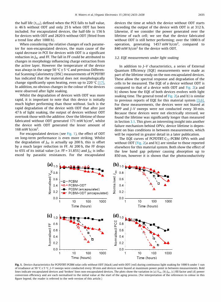
3.2. EQE measurements under light soaking
In addition to J–V characteristics, a series of ExternalQuantum Efficiency (EQE) measurements were made aspart of the lifetime study on the non-encapsulated devices.These allow the spectral response and degradation of thecells to be measured. The EQE of a device without ODT iscompared to that of a device with ODT and Fig. 2(a andb) shows how the EQE of both devices evolves with lightsoaking time. The general trend of Fig. 2(a and b) is similarto previous reports of EQE for this material system [3,6].For these measurements, the devices were not biased atMPP and J–V sweeps were not conducted every 30 min.Because these devices were not electrically stressed, wefound the lifetime was significantly longer than measuredin Section 3.1. This gives an interesting insight into anotherfailure mechanism behind OPVs; device lifetime is depen-dent on bias conditions in between measurements, whichwill be reported in greater detail in a later publication.
The EQE curves of PCPDTBT:C71-PCBM OPVs with andwithout ODT (Fig. 2(a and b)) are similar to those reportedelsewhere for this material system. Both show the effect ofthe low band gap polymer causing absorption up to850 nm, however it is shown that the photoconductivity
nd with ODT (red) during continuous light soaking for 1000 h under 1 sunes were biased at maximum power point in between measurements. BoldThe plots show the variation in (a) VOC, (b) JSC, (c) fill factor and (d) powerf the aging process. (For interpretation of the references to colour in this

Fig. 2. External Quantum Efficiency (EQE) characteristics for non-encap-sulated PCPDTBT:PCBM solar cells (a) with ODT and (b) without ODTduring continuous light soaking for 800 h under 1 sun of irradiance at50 �C. The time dependence of the EQE peaks at 483 nm and 793 nm(corresponding to peak C71-PCBM and PCPDTBT absorption) for deviceswith ODT and without ODT are shown in (c).
Fig. 3. Atomic Force Microscope (AFM) topography of PCPDTBT:C71-PCBM OPVs with ODT (a) before light soaking and (b) after light soakingand PCPDTBT:C71-PCBM OPVs without ODT (c) before light soaking and(d) after light soaking. From measurements of surface roughness, a largerrelative change in morphology of devices fabricated with ODT is observed.
2436 H. Waters et al. / Organic Electronics 15 (2014) 2433–2438
response increases strongly by incorporating ODT to thesolution [18–20]. As the devices are light soaked, the gen-eral shape of the curves only change slightly, indicatingthat PCPDTBT and C71-PCBM in the active layer are degrad-ing at only slightly different rates. The peak polymerabsorption (793 nm) and the wavelength where C71-PCBMabsorption dominates (483 nm) are plotted for devicesmade with and without ODT, shown in Fig. 2(c). The overalldegradation rates are much slower than in Section 3.1 asthe devices are not being electrically stressed by biasingin between measurements or undergoing J–V measure-ments at regular intervals. It is shown that devices withODT degrade possess a much lower intrinsic stability anddo so more rapidly than devices without ODT. In addition,both PCPDTBT:C71-PCBM devices showed slower degrada-tion at the k = 793 nm, corresponding to the PCPDTBTabsorption, than at k = 483 nm, indicating that C71-PCBMis the less stable component of the active layer (see Fig. 3).
3.3. Morphological characterisation
To judge whether the ODT facilitates an additional deg-radation route, AFM images of the surfaces of non-encapsu-lated devices with and without ODT and before and afterlight soaking for 250 h were undertaken and are shown inFig. 4. For typical devices with ODT, the initial surfaceroughness (RA) was measured at 1.11 nm and the peak-to-peak roughness measured (RMAX) at 9.35 nm. After lightsoaking, this reduced to RA = 0.63 nm and RMAX = 7.08 m, arelative decrease of 44% and 25%, respectively. By compar-ison a device without ODT prior to light soaking had asurface roughness of 0.55 nm and peak to peak value of7.83 nm, which reduced to RA = 0.47 nm and RMAX = 7.62 nm,relative changes of 16% and 3%, respectively.
For further understanding of the structural changes thatoccur as a result of ODT inclusion in the active layer, weinvestigated the effect of light soaking on morphologyusing small- and wide-angle X-ray scattering (GISAXS/GIWAXS) at the National Synchrotron Radiation ResearchCenter, Taiwan. Experimental setup is discussed elsewhere[20,21]. These layers were prepared in the same manner asthe layers used for devices as reported in Sections 3.1 and3.2, so were prepared onto PEDOT:PSS-coated glasssubstrates. Fig. 4(a) shows in-plane GISAXS profiles (20)measured for the active layers of PCPDTBT:C71-PCBMwith/without ODT and before and after light soaking for300 h. Prior to light soaking, the GISAXS profiles of activelayers with/without ODT very closely overlap. FromFig. 4(a), it was seen that light soaking resulted inincreased scattering intensity at 0.004–0.002 Å�1 (150–300 nm) for both layers with/without ODT, revealing a rel-atively large scale PCBM agglomeration [22,23]. Howeverfor the layers processed with ODT, scattering intensity inthe higher-q region (>0.01 Å�1) is enhanced substantially(10–20 nm), which corresponds to smaller and compact

H. Waters et al. / Organic Electronics 15 (2014) 2433–2438 2437
C71-PCBM aggregates of an average size of 14 nm, asrevealed from the sphere model fitting shown in Fig. 4(a)[21,22,24]. It is evident that morphology of the active layerprocessed with ODT is relatively unstable to light soaking.
Fig. 4(b) shows the corresponding normal-to-planeGIWAXS profiles for the same samples. The halo peak cen-ters at 1.30 Å�1 for the film processed without ODT movesto 1.15 Å�1 for the film with ODT, revealing a substantialincrease of an intermolecular distance of PCBM (22) from4.8 Å to 5.5 Å. This effect may be attributed to less aggre-gated (or more disperse) C71-PCBM in the film when spincoated with ODT (22). After light soaking, the intermolecu-lar distance for the sample with ODT decreased from 5.5 Åto 5.3 Å (the halo peak moved from 1.15 to 1.20 Å�1 inFig. 4b), together with a substantially enhanced intensity,suggesting a stronger PCBM aggregation. In contrast, thereis less changes in the halo peak for the film processed with-out ODT. Overall, the film processed with ODT exhibitedlarger local and global morphological changes associatedclosely to PCBM.
0.01 0.1
1
10
100
1000
Rel
ativ
e In
tens
ity
qxy (Å-1)
With ODT With ODT / Light Soaking No ODT
No ODT / Light Soaking
0.003 0.2
(a)
0.5 1 1.5 2
500
1000
1500
1.30
1.20 Å-1
With ODT With ODT / Light Soaking
No ODT No ODT / Light Soaking
Rel
ativ
e In
tens
ity
qz (Å-1)
1.15
0.3
(b)
Fig. 4. (a) GISAX and (b) GIWAX profiles of PCPDTBT:C71-PCBM activelayers with /without ODT and before/after light soaking for 300 h. Thearrows in (a) and (b) depict the characteristic intensity growths indifferent in-plane qxy-region and normal-to-plane qz resulted from lightsoaking, which indicates that films prepared with ODT undergo moresubstantial morphological changes. The GISAXS data for the film withODT and subject to light soaking in (a) are fitted (solid curve) with amodel of spherical PCBM aggregates of an average diameter 14 ± 2 nm,with 5% polydispersity in the higher-q regime (>0.01 Å�1), together with afractal agglomeration of a correlation length of 134 nm and a fractaldimension of 2.4 in the low-q region.
It is clear that from AFM data and the GISAXS/GIWAXSmeasurements that the morphological change induced bylight soaking is greater when ODT has been included.ODT possesses a high boiling point of 269 �C and is unlikelyto be evaporated at the low processing temperatures usedin device fabrication, or even under the high vacuum forCa/Al contact evaporation. It is therefore likely that someODT remains in the active layer when devices are removedfrom the evaporation chamber and lifetime tests start. Thisconclusion is supported by Cho et al. [9], who showed thatthe ODT was not completely removed from the active layerfilms by placing them in high vacuum (�10�6 Torr). Resid-ual ODT left in the active layer will selectively dissolve theC71-PCBM component, as the PCPDTBT is less soluble inODT [6] and will lead to increased aggregation and a reduc-tion in the connectivity of C71-PCBM percolation networks,thus limiting the amount of charge that can be extractedfrom the active layer. Therefore, in order to have stablePCPDTBT:C71-PCBM devices made using ODT, it might benecessary to remove the ODT after processing. This couldpose difficulties as ODT has a high boiling point andPCPDTBT:C71-PCBM OPVs tend to decrease in performancewith higher temperature annealing/baking steps [2]. Analternative is to use a crosslinkable PCPDTBT analogue tostabilize the film morphology optimised by ODT duringspincasting, thereby, a sustainable high PCE performanceupon light soaking.
4. Conclusions
It has been demonstrated that the inclusion of ODT inthe active layer during the fabrication of PCPDTBT-basedOPV devices led to a reduced overall performance underlight soaking. Measurements of the FF as well as AFMand GISAXS-GIWAXS studies indicate that, while the incor-poration of ODT during processing enhances the initial per-formance with an optimised morphology, it leads togreater and apparently detrimental changes in the mor-phology, when subject to long-term light soaking. Boththe additive effects on morphology optimisation andlong-term stability subject to light soaking, of the activelayers, require balanced considerations.
Acknowledgements
All authors would like to thank the Prof. T.J. Lewis forhis advice and valuable insight whilst preparing this paper.Noel Bristow and Dr. Omar Moudam are grateful for finan-cial support from the Wales Ireland Network for InnovativePhotovoltaic Technologies (WIN-IPT) project, fundedthrough the Interreg 4A, Wales Ireland Programme 2007-13. Huw Waters would like to thank Bangor Universityfor financial support through the 125 Anniversary scholar-ship fund.
References
[1] Johannes Hachmann, Roberto Olivares-Amaya, Adrian Jinich,Anthony L. Appleton, Martin A. Blood-Forsythe, László R. Seress,Carolina Román-Salgado, et al., Lead candidates for high-performance organic photovoltaics from high-throughput quantum

2438 H. Waters et al. / Organic Electronics 15 (2014) 2433–2438
chemistry–the Harvard Clean Energy Project, Energy Environ. Sci. 7(2) (2014) 698–704.
[2] J. Kettle, M. Horie, L.A. Majewski, B.R. Saunders, S. Tuladhar, J. Nelson,M.L. Turner, Optimisation of PCPDTBT solar cells using polymersynthesis with Suzuki coupling, Sol. Energy Mater. Sol. Cells 95 (8)(2011) 2186–2193.
[3] Jeffrey Peet, Michelle L. Senatore, Alan J. Heeger, Guillermo C. Bazan,The role of processing in the fabrication and optimization of plasticsolar cells, Adv. Mater. 21 (14–15) (2009) 1521–1527.
[4] Tracey M. Clarke, Amy M. Ballantyne, Jenny Nelson, Donal D.C.Bradley, James R. Durrant, Free energy control of chargephotogeneration in polythiophene/fullerene solar cells: theinfluence of thermal annealing on P3HT/PCBM blends, Adv. Funct.Mater. 18 (24) (2008) 4029–4035.
[5] Dian Chen, Atsuhiro Nakahara, Dongguang Wei, Dennis Nordlund,Thomas P. Russell, P3HT/PCBM bulk heterojunction organicphotovoltaics: correlating efficiency and morphology, Nano Lett. 11(2) (2010) 561–567.
[6] Jae Kwan Lee, Wan Li Ma, Christoph J. Brabec, Jonathan Yuen, Ji SunMoon, Jin Young Kim, Kwanghee Lee, Guillermo C. Bazan, Alan J.Heeger, Processing additives for improved efficiency from bulkheterojunction solar cells, J. Am. Chem. Soc. 130 (11) (2008) 3619–3623.
[7] Jeffery Peet, J.Y. Kim, Nelson E. Coates, Wang Li Ma, Daniel Moses,Alan J. Heeger, Guillermo C. Bazan, Efficiency enhancement in low-bandgap polymer solar cells by processing with alkane dithiols, Nat.Mater. 6 (7) (2007) 497–500.
[8] Jeffrey Peet, Alan J. Heeger, Guillermo C. Bazan, ‘‘Plastic’’ solar cells:self-assembly of bulk heterojunction nanomaterials by spontaneousphase separation, Acc. Chem. Res. 42 (11) (2009) 1700–1708.
[9] Shinuk Cho, Jae Kwan Lee, Ji Sun Moon, Jonathan Yuen, KwangheeLee, Alan J. Heeger, Bulk heterojunction bipolar field-effecttransistors processed with alkane dithiol, Org. Electron. 9 (6)(2008) 1107–1111.
[10] Jingbi You, Letian Dou, Ken Yoshimura, Takehito Kato, KenichiroOhya, Tom Moriarty, Keith Emery, et al., Nat. Commun. 4 (2013)1446.
[11] James T. Rogers, Kristin Schmidt, Michael F. Toney, Edward J.Kramer, Guillermo C. Bazan, Structural order in bulkheterojunction films prepared with solvent additives, Adv. Mater.23 (20) (2011) 2284–2288.
[12] Almantas Pivrikas, Helmut Neugebauer, Niyazi Serdar Sariciftci,Influence of processing additives to nano-morphology and efficiencyof bulk-heterojunction solar cells: a comparative ⁄review, Sol.Energy 85 (6) (2011) 1226–1237.
[13] Shu-Wei Chang, Huw Waters, Jeff Kettle, Zi-Rui Kuo, Chun-Han Li,Chin-Yang Yu, Masaki Horie, Pd-catalysed direct arylation
polymerisation for synthesis of low-bandgap conjugated polymersand photovoltaic performance, Macromol. Rapid Commun. 33 (22)(2012) 1927–1932.
[14] J. Kettle, H. Waters, M. Horie, S.W. Chang, Effect of hole transportinglayers on the performance of PCPDTBT: PCBM organic solar cells, J.Phys. D Appl. Phys. 45 (12) (2012) 125102.
[15] Matthew O. Reese, Suren A. Gevorgyan, Mikkel Jørgensen, EvaBundgaard, Sarah R. Kurtz, David S. Ginley, Dana C. Olson, et al.,Consensus stability testing protocols for organic photovoltaicmaterials and devices, Sol. Energy Mater. Sol. Cells 95 (5) (2011)1253–1267.
[16] Mikkel Jørgensen, Kion Norrman, Frederik C. Krebs, Stability/degradation of polymer solar cells, Sol. Energy Mater. Sol. Cells 92(7) (2008) 686–714.
[17] W.J. Potscavage, S. Yoo, Benoit Domercq, Bernard Kippelen,Encapsulation of pentacene/C organic solar cells with AlOdeposited by atomic layer deposition, Appl. Phys. Lett. 90 (2007)253511.
[18] M. Horie, L.A. Majewski, M.J. Fearn, C.-Y. Yu, Y. Luo, A. Song, B.R.Saunders, M.L. Turner, Cyclopentadithiophene based polymers – acomparison of optical, electrochemical and organic field-Effecttransistor characteristics, J. Mater. Chem. 20 (2010) 4347–4355.
[19] Almantas Pivrikas, Helmut Neugebauer, Niyazi Serdar Sariciftci,Charge carrier lifetime and recombination in bulk heterojunctionsolar cells, IEEE J. Sel. Top. Quant. Electron. 16 (6) (2010) 1746–1758.
[20] Nelson E. Coates, In-Wook Hwang, Jeffrey Peet, Guillermo C. Bazan,Daniel Moses, Alan J. Heeger, 1,8-octanedithiol as a processingadditive for bulk heterojunction materials: enhancedphotoconductive response, Appl. Phys. Lett. 93 (7) (2008). 072105.
[21] U. Jeng, C.-H. Su, C.-J. Su, K.-F. Liao, W.-T. Chuang, K.-S. Liang, Asmall/wide-angle X-ray scattering instrument for structuralcharacterization of air-liquid interfaces, thin films, and bulkspecimens, J. Appl. Crystallogr. 43 (2010) 110–121.
[22] W.-R. Wu, U. Jeng, C.-J. Su, K.-H. Wei, M.-S. Su, M.-Y. Chiu, A.-C. Su,Competition between fullerene aggregation and poly(3-hexylthiophene) crystallization upon annealing of bulkheterojunction solar cells, ACS Nano 5 (2011) 6233–6243.
[23] H. Waters, J. Kettle, S.W. Chang, C.J. Su, W.R. Wu, U.S. Jeng, M. Horie,Organic photovoltaics based on a crosslinkable PCPDTBT analogue;synthesis, morphological studies, solar cell performance andenhanced lifetime, J. Mater. Chem. A 1 (25) (2013) 7370–7378.
[24] M.S. Su, C.Y. Kuo, M.C. Yuan, U. Jeng, C.J. Su, K.H. Wei, Improvingdevice efficiency of polymer/fullerene bulk heterojunction solar cellsthrough enhanced crystallinity and reduced grain boundariesinduced by solvent additives, Adv. Mater. 23 (29) (2011) 3315–3319.