Embed Size (px)
Citation preview
EVAL-ADAQ8088EBZ User Guide UG-1825
One Technology Way • P.O. Box 9106 • Norwood, MA 02062-9106, U.S.A. • Tel: 781.329.4700 • Fax: 781.461.3113 • www.analog.com
Evaluating the ADAQ8088 Dual-, Differential, Low-Pass Filter μModule
with Gain and ADC Driver
PLEASE SEE THE LAST PAGE FOR AN IMPORTANT WARNING AND LEGAL TERMS AND CONDITIONS. Rev. 0 | Page 1 of 12
FEATURES 3 common signal processing and conditioning blocks, a
preamplifier, an 8-pole filter, and an ADC driver integrated to support a variety of demodulator applications
No external components required for proper operation
EVALUATION KIT CONTENTS EVAL-ADAQ8088EBZ evaluation board
EQUIPMENT NEEDED Bench supply of 2.7 V to 3.3 V SMA cables 4-Port or 2-port network analyzer AD9681-125EBZ evaluation kit HSC-ADC-EVALEZ evaluation kit Keysight 33600A generator Allen Avionics LPF #F3056-7P7 (2 pieces) PC running Windows®
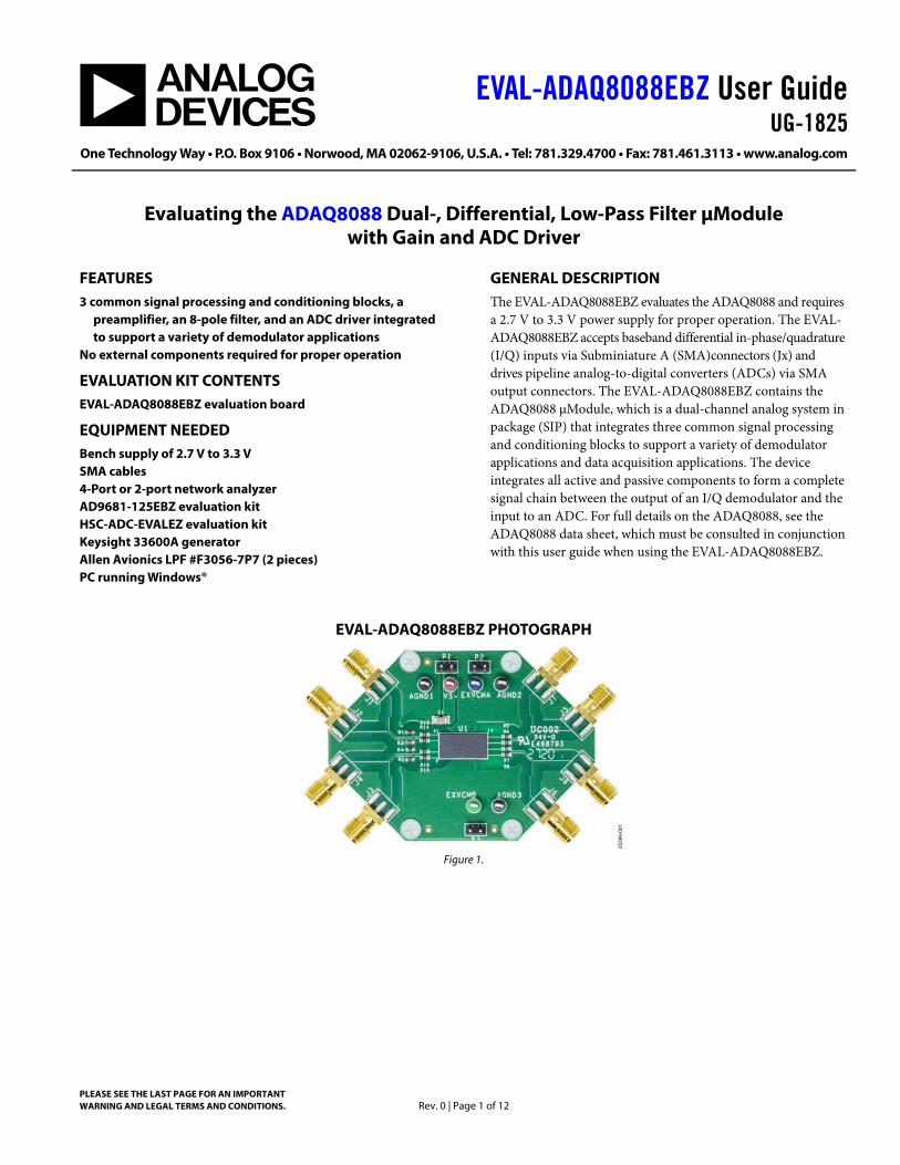
GENERAL DESCRIPTION The EVAL-ADAQ8088EBZ evaluates the ADAQ8088 and requires a 2.7 V to 3.3 V power supply for proper operation. The EVAL-ADAQ8088EBZ accepts baseband differential in-phase/quadrature (I/Q) inputs via Subminiature A (SMA)connectors (Jx) and drives pipeline analog-to-digital converters (ADCs) via SMA output connectors. The EVAL-ADAQ8088EBZ contains the ADAQ8088 μModule, which is a dual-channel analog system in package (SIP) that integrates three common signal processing and conditioning blocks to support a variety of demodulator applications and data acquisition applications. The device integrates all active and passive components to form a complete signal chain between the output of an I/Q demodulator and the input to an ADC. For full details on the ADAQ8088, see the ADAQ8088 data sheet, which must be consulted in conjunction with this user guide when using the EVAL-ADAQ8088EBZ.
EVAL-ADAQ8088EBZ PHOTOGRAPH
Figure 1.
25
39
9-0
01
UG-1825 EVAL-ADAQ8088EBZ User Guide
Rev. 0 | Page 2 of 12
TABLE OF CONTENTS Features .............................................................................................. 1
Evaluation Kit Contents ................................................................... 1
Equipment Needed ........................................................................... 1
General Description ......................................................................... 1
EVAL-ADAQ8088EBZ Photograph ............................................... 1
Revision History ............................................................................... 2
Evaluation Board Hardware ............................................................ 3
Setting Up the Evaluation Board ................................................ 3
Analog Inputs ................................................................................ 3
Magnitude and Phase Response Measurements Using A Four-Port Network Analyzer .................................................................... 4
Measuring the Magnitude and Phase of the I-Channel .......... 4
Measuring the Magnitude and Phase of the Q-Channel......... 4
Calibration Procedure .................................................................. 4
Magnitude and Frequency Response Measurements Using A Two-Port Network Analyzer ........................................................... 5
Measuring the Magnitude and Frequency Response of the I-Channel ...........................................................................................5
Measuring the Magnitude and Frequency Response of the Q-Channel ...........................................................................................6
Calibration Procedure ..................................................................6
Evaluating the ADAQ8088 by Driving the AD9681 ADC ..........7
Configuring the EVAL-ADAQ8088EBZ, AD9681-125EBZ, and HSC-ADC-EVALEZ ...............................................................7
Measurement Results when Driving the AD9681 Using the ADAQ8088 as a Driver .................................................................7
Troubleshooting Tips ....................................................................8
Evaluation Board Schematics and Artwork ...................................9
Ordering Information .................................................................... 12
Bill of Materials ........................................................................... 12
REVISION HISTORY 3/2021—Revision 0: Initial Version
EVAL-ADAQ8088EBZ User Guide UG-1825
Rev. 0 | Page 3 of 12
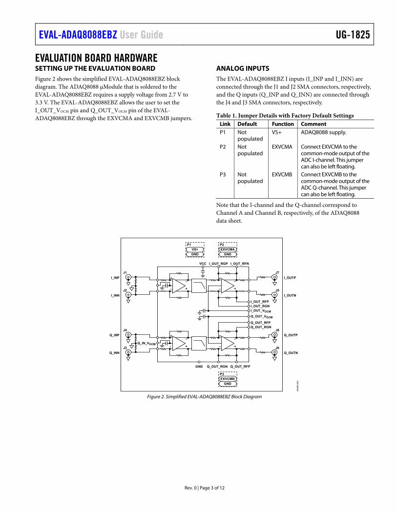
EVALUATION BOARD HARDWARE SETTING UP THE EVALUATION BOARD Figure 2 shows the simplified EVAL-ADAQ8088EBZ block diagram. The ADAQ8088 μModule that is soldered to the EVAL-ADAQ8088EBZ requires a supply voltage from 2.7 V to 3.3 V. The EVAL-ADAQ8088EBZ allows the user to set the I_OUT_VOCM pin and Q_OUT_VOCM pin of the EVAL-ADAQ8088EBZ through the EXVCMA and EXVCMB jumpers.
ANALOG INPUTS The EVAL-ADAQ8088EBZ I inputs (I_INP and I_INN) are connected through the J1 and J2 SMA connectors, respectively, and the Q inputs (Q_INP and Q_INN) are connected through the J4 and J3 SMA connectors, respectively.
Table 1. Jumper Details with Factory Default Settings Link Default Function Comment P1 Not
populated VS+ ADAQ8088 supply.
P2 Not populated
EXVCMA Connect EXVCMA to the common-mode output of the ADC I-channel. This jumper can also be left floating.
P3 Not populated
EXVCMB Connect EXVCMB to the common-mode output of the ADC Q-channel. This jumper can also be left floating.
Note that the I-channel and the Q-channel correspond to Channel A and Channel B, respectively, of the ADAQ8088 data sheet.
Figure 2. Simplified EVAL-ADAQ8088EBZ Block Diagram
+
+–
–+
+–
–
VCC I_OUT_RGP I_OUT_RFN
I_OUT_RFPI_OUT_RGN
Q_OUT_RFPQ_OUT_RGN
I_OUT_VOCM
Q_OUT_VOCM
Q_IN_VOCM
J4
J3
+
+–
–+
+–
–
Q_OUT_RGN Q_OUT_RFPGND
J8
J6
J1
J2
Q_INP
Q_INN
I_INP
I_INN
Q_OUTP
Q_OUTN
I_OUTP
I_OUTN
J7
J5
EXVCMA
GND
P2
EXVCMB
GND
P3
VS+
GND
P1
253
99
-00
2
UG-1825 EVAL-ADAQ8088EBZ User Guide
Rev. 0 | Page 4 of 12
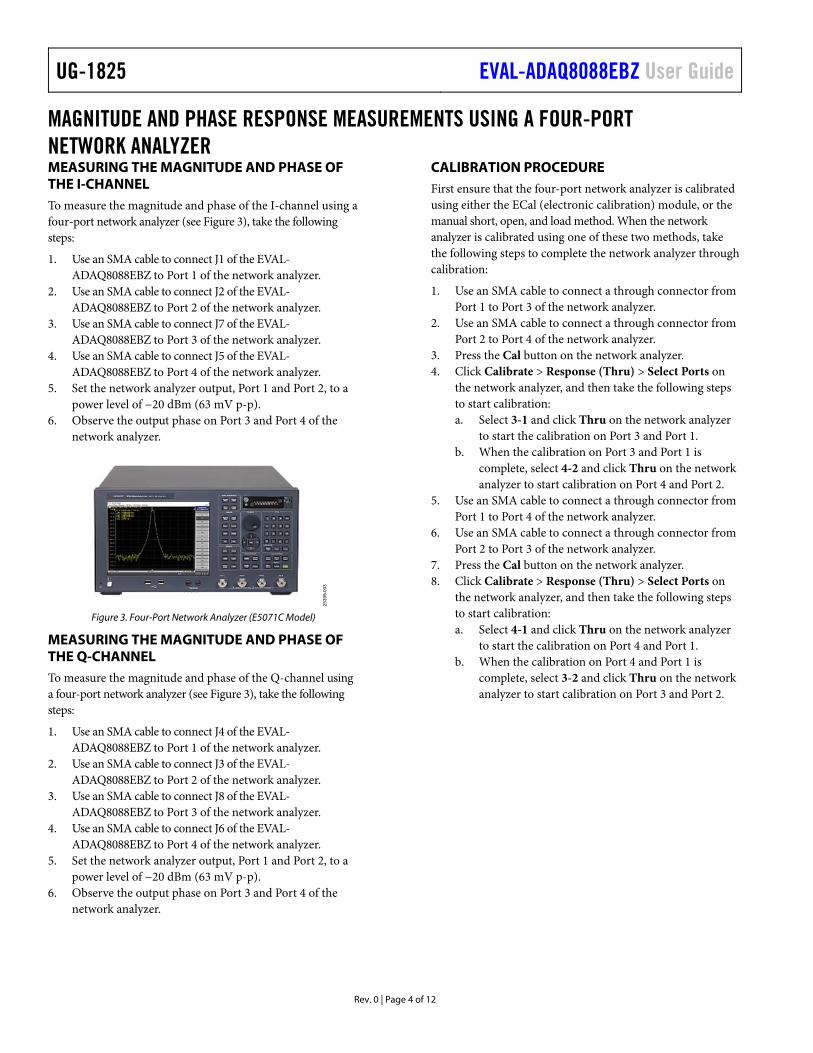
MAGNITUDE AND PHASE RESPONSE MEASUREMENTS USING A FOUR-PORT NETWORK ANALYZER MEASURING THE MAGNITUDE AND PHASE OF THE I-CHANNEL To measure the magnitude and phase of the I-channel using a four-port network analyzer (see Figure 3), take the following steps:
1. Use an SMA cable to connect J1 of the EVAL-ADAQ8088EBZ to Port 1 of the network analyzer.
2. Use an SMA cable to connect J2 of the EVAL-ADAQ8088EBZ to Port 2 of the network analyzer.
3. Use an SMA cable to connect J7 of the EVAL-ADAQ8088EBZ to Port 3 of the network analyzer.
4. Use an SMA cable to connect J5 of the EVAL-ADAQ8088EBZ to Port 4 of the network analyzer.
5. Set the network analyzer output, Port 1 and Port 2, to a power level of −20 dBm (63 mV p-p).
6. Observe the output phase on Port 3 and Port 4 of the network analyzer.
Figure 3. Four-Port Network Analyzer (E5071C Model)
MEASURING THE MAGNITUDE AND PHASE OF THE Q-CHANNEL To measure the magnitude and phase of the Q-channel using a four-port network analyzer (see Figure 3), take the following steps:
1. Use an SMA cable to connect J4 of the EVAL-ADAQ8088EBZ to Port 1 of the network analyzer.
2. Use an SMA cable to connect J3 of the EVAL-ADAQ8088EBZ to Port 2 of the network analyzer.
3. Use an SMA cable to connect J8 of the EVAL-ADAQ8088EBZ to Port 3 of the network analyzer.
4. Use an SMA cable to connect J6 of the EVAL-ADAQ8088EBZ to Port 4 of the network analyzer.
5. Set the network analyzer output, Port 1 and Port 2, to a power level of −20 dBm (63 mV p-p).
6. Observe the output phase on Port 3 and Port 4 of the network analyzer.
CALIBRATION PROCEDURE First ensure that the four-port network analyzer is calibrated using either the ECal (electronic calibration) module, or the manual short, open, and load method. When the network analyzer is calibrated using one of these two methods, take the following steps to complete the network analyzer through calibration:
1. Use an SMA cable to connect a through connector from Port 1 to Port 3 of the network analyzer.
2. Use an SMA cable to connect a through connector from Port 2 to Port 4 of the network analyzer.
3. Press the Cal button on the network analyzer. 4. Click Calibrate > Response (Thru) > Select Ports on
the network analyzer, and then take the following steps to start calibration: a. Select 3-1 and click Thru on the network analyzer
to start the calibration on Port 3 and Port 1. b. When the calibration on Port 3 and Port 1 is
complete, select 4-2 and click Thru on the network analyzer to start calibration on Port 4 and Port 2.
5. Use an SMA cable to connect a through connector from Port 1 to Port 4 of the network analyzer.
6. Use an SMA cable to connect a through connector from Port 2 to Port 3 of the network analyzer.
7. Press the Cal button on the network analyzer. 8. Click Calibrate > Response (Thru) > Select Ports on
the network analyzer, and then take the following steps to start calibration: a. Select 4-1 and click Thru on the network analyzer
to start the calibration on Port 4 and Port 1. b. When the calibration on Port 4 and Port 1 is
complete, select 3-2 and click Thru on the network analyzer to start calibration on Port 3 and Port 2.
25
39
9-0
03
EVAL-ADAQ8088EBZ User Guide UG-1825
Rev. 0 | Page 5 of 12
MAGNITUDE AND FREQUENCY RESPONSE MEASUREMENTS USING A TWO-PORT NETWORK ANALYZER MEASURING THE MAGNITUDE AND FREQUENCY RESPONSE OF THE I-CHANNEL I_INP as the Active Input To measure the magnitude and frequency response of the I-channel with the I_INP input as the active input and using a two-port network analyzer (see Figure 4), take the following steps: 1. Use an SMA cable to connect J1 of the EVAL-
ADAQ8088EBZ to Port 1 of the network analyzer. 2. Leave J2 of the EVAL-ADAQ8088EBZ floating. 3. To measure the frequency response at the I_OUTP
output of the EVAL-ADAQ8088EBZ, take the following steps: a. Use an SMA cable to connect J7 of the EVAL-
ADAQ8088EBZ to Port 2 of the network analyzer. b. Terminate J5 to 50 Ω. c. Set the network analyzer output, Port 1, to a power
level of −20 dBm. d. Observe the frequency response on Port 2 of the
network analyzer. 4. To measure the frequency response at the I_OUTN
output of the EVAL-ADAQ8088EBZ, take the following steps: a. Use an SMA cable to connect J5 of the EVAL-
ADAQ8088EBZ to Port 2 of the network analyzer. b. Terminate J7 to 50 Ω. c. Set the network analyzer output, Port 1, to a power
level of −20 dBm. d. Observe the frequency response on Port 2 of the
network analyzer.
I_INN as the Active Input To measure the magnitude and frequency response of the I-channel with the I_INN input as the active input and using a two-port network analyzer (see Figure 4), take the following steps: 1. Use an SMA cable to connect J2 of the EVAL-
ADAQ8088EBZ to Port 1 of the network analyzer. 2. Leave J1 of the EVAL-ADAQ8088EBZ floating. 3. To measure the frequency response at the I_OUTP and
I_OUTN outputs of the EVAL-ADAQ8088EBZ, repeat Step 3 and Step 4 of the procedure in the I_INP as the Active Input section.
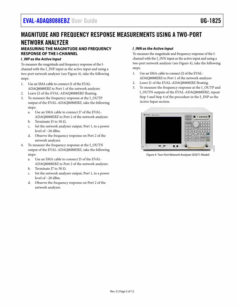
Figure 4. Two-Port Network Analyzer (E5071 Model)
25
39
9-0
05
UG-1825 EVAL-ADAQ8088EBZ User Guide
Rev. 0 | Page 6 of 12
MEASURING THE MAGNITUDE AND FREQUENCY RESPONSE OF THE Q-CHANNEL Q_INP as the Active Input To measure the magnitude and frequency response of the Q-channel with the Q_INP input as the active input and using a two-port network analyzer (see Figure 4), take the following steps: 1. Use an SMA cable to connect J4 of the EVAL-
ADAQ8088EBZ to Port 1 of the network analyzer. 2. Leave J3 of the EVAL-ADAQ8088EBZ floating. 3. To measure the frequency response at the Q_OUTP
output of the EVAL-ADAQ8088EBZ, take the following steps: a. Use an SMA cable to connect J8 of the EVAL-
ADAQ8088EBZ to Port 2 of the network analyzer. b. Terminate J6 to 50 Ω. c. Set the network analyzer output, Port 1, to a power
level of −20 dBm. d. Observe the frequency response on Port 2 of the
network analyzer. 4. To measure the frequency response at the Q_OUTP
output of the EVAL-ADAQ8088EBZ, take the following steps: a. Use an SMA cable to connect J6 of the EVAL-
ADAQ8088EBZ to Port 2 of the network analyzer. b. Terminate J8 to 50 Ω. c. Set the network analyzer output, Port 1, to a power
level of −20 dBm. d. Observe the frequency response on Port 2 of the
network analyzer.
Q_INN as the Active Input To measure the magnitude and frequency response of the Q-channel with the Q_INN input as the active input and using a two-port network analyzer (see Figure 4), take the following steps: 1. Use an SMA cable to connect J3 of the EVAL-
ADAQ8088EBZ to Port 1 of the network analyzer. 2. Leave J4 of the EVAL-ADAQ8088EBZ floating. 3. To measure the frequency response at the Q_OUTP and
Q_OUTN outputs of the EVAL-ADAQ8088EBZ, repeat Step 3 and Step 4 of the procedure in the Q_INP as the Active Input section.
CALIBRATION PROCEDURE First ensure that the two-port network analyzer is calibrated using either the ECal (electronic calibration) module, or the manual short, open, and load method. When the network analyzer is calibrated using one of these two methods, take the following steps to complete the network analyzer through calibration: 1. Use an SMA cable to connect a through connector from
Port 1 to Port 2 of the network analyzer. 2. Press the Cal button on the network analyzer. 3. Click Calibrate > Response (Thru) > Select Ports on
the network analyzer. 4. Select 2-1, and click Thru.
EVAL-ADAQ8088EBZ User Guide UG-1825
Rev. 0 | Page 7 of 12
EVALUATING THE ADAQ8088 BY DRIVING THE AD9681 ADC CONFIGURING THE EVAL-ADAQ8088EBZ, AD9681-125EBZ, AND HSC-ADC-EVALEZ Before using the software for testing, take the following steps to configure the EVAL-ADAQ8088EBZ, AD9681-125EBZ, and HSC-ADC-EVALEZ:
1. Take the following steps to modify the EVAL-ADAQ8088EBZ: a. Remove the R5, R6, R7, and R8 resistors. b. Install a 40 Ω resistor on R5, R6, R7, and R8.
2. Take the following steps to modify the AD9681-125EBZ (FMC connector version) of each channel selected (Figure 6 shows Channel A1 and Channel A2 selected for use): a. Install an SMA connector on the J102 and J104
ports. b. Remove the R14, R16, C3, C4, J6, J7, C7 to C10,
R36, to R39, and T17 to T20. c. Install a 0 Ω resistor on R321, R415, C3, C4, J6, J7,
C7 to C10, and R36 to R39. d. Connect a jumper wire from Pin 3 to Pin 4 of T1. e. Connect a jumper wire from Pin 1 to Pin 6 of T1. f. Connect a jumper wire from Pin 3 to Pin 4 of T2. g. Connect a jumper wire from Pin 1 to Pin 6 of T2.
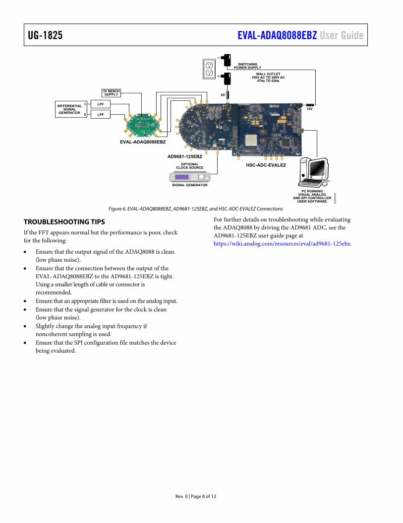
3. Connect the EVAL-ADAQ8088EBZ to the AD9681-125EBZ, as shown in Figure 6, and then connect the AD9681-125EBZ to the HSC-ADC-EVALEZ by aligning each of their field programmable gate array mezzanine card (FMC) connector and carefully press them together. Note that FMC connectors often come from the factory with a sticker that prevents connection. Remove this sticker (if needed) before attempting to make the connection.
4. On the EVAL-ADAQ8088EBZ, confirm that the jumpers are installed as shown in Figure 8.
5. Connect one 6 V, 2.5 A switching power supply (such as the CUI, Inc., EPS060250UH-PHP-SZ supplied in the AD9681-125EBZ evaluation kit) to the AD9681-125EBZ.
6. Connect the 12 V, 3.3 A switching power supply to the HSC-ADC-EVALEZ board.
7. Connect the HSC-ADC-EVALEZ to the PC using a USB cable (supplied in the HSC-ADC-EVALEZ evaluation kit).
8. On the EVAL-ADAQ8088EBZ, replace the value of R5, R6, R7, and R8 with 40 Ω each and use a clean signal generator with low phase noise to provide an input signal.
9. Connect the output signal from either J5 and J7 or J6 and J8 to the selected channel of the AD9681-125EBZ.
MEASUREMENT RESULTS WHEN DRIVING THE AD9681 USING THE ADAQ8088 AS A DRIVER The configurations of the EVAL-ADAQ8088EBZ and the AD9681-125EBZ used during testing include the following:
The input source dual-channel generator (Keysight 33600A differential signal generator) is set to 6 MHz, 52 mV p-p for −1 dbFS.
The input filter (Allen Avionics low-pass filter (LPF), F3056-7P7) is set to a 7.7 MHz cutoff frequency. Another LPF can be selected with a cutoff frequency above the input frequency and below the first harmonic.
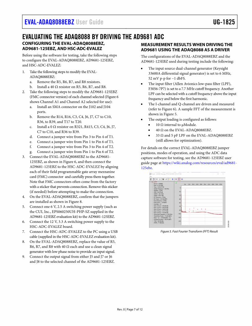
The I-channel and Q-channel are driven and measured (refer to Figure 6). A sample FFT of the measurement is shown in Figure 5.
The output loading is configured as follows: 10 Ω internal to μModule. 40 Ω on the EVAL-ADAQ8088EBZ. 33 Ω and 5 pF LPF on the EVAL-ADAQ8088EBZ
(still allows for optimization).
For details on the correct EVAL-ADAQ8088EBZ jumper positions, modes of operation, and using the ADC data capture software for testing, see the AD9681-125EBZ user guide page at https://wiki.analog.com/resources/eval/ad9681-125ebz.
Figure 5. Fast Fourier Transform (FFT) Result
25
39
9-0
08
UG-1825 EVAL-ADAQ8088EBZ User Guide
Rev. 0 | Page 8 of 12
Figure 6. EVAL-ADAQ8088EBZ, AD9681-125EBZ, and HSC-ADC-EVALEZ Connections
TROUBLESHOOTING TIPS If the FFT appears normal but the performance is poor, check for the following:
Ensure that the output signal of the ADAQ8088 is clean (low phase noise).
Ensure that the connection between the output of the EVAL-ADAQ8088EBZ to the AD9681-125EBZ is tight. Using a smaller length of cable or connector is recommended.
Ensure that an appropriate filter is used on the analog input. Ensure that the signal generator for the clock is clean
(low phase noise). Slightly change the analog input frequency if
noncoherent sampling is used. Ensure that the SPI configuration file matches the device
being evaluated.
For further details on troubleshooting while evaluating the ADAQ8088 by driving the AD9681 ADC, see the AD9681-125EBZ user guide page at https://wiki.analog.com/resources/eval/ad9681-125ebz.
253
99
-00
6
3V BENCHSUPPLY
EVAL-ADAQ8088EBZ
AD9681-125EBZ
HSC-ADC-EVALEZ
LPFDIFFERENTIALSIGNAL
GENERATOR
1
2 LPF
SIGNAL GENERATOR
OPTIONALCLOCK SOURCE
PC RUNNINGVISUAL ANALOG
AND SPI CONTROLLERUSER SOFTWARE
SWITCHINGPOWER SUPPLY
WALL OUTLET100V AC TO 240V AC
47Hz TO 63Hz
6V
12V
EVAL-ADAQ8088EBZ User Guide UG-1825
Rev. 0 | Page 9 of 12
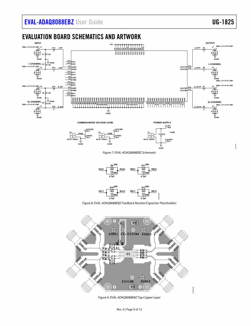
EVALUATION BOARD SCHEMATICS AND ARTWORK
Figure 7. EVAL-ADAQ8088EBZ Schematic
Figure 8. EVAL-ADAQ8088EBZ Feedback Resistor/Capacitor Placeholders
Figure 9. EVAL-ADAQ8088EBZ Top Copper Layer
A12
VS+
RA21A13
RA22A1
VINAPC1
VINANC12
RA11C132
1
3 4 5RA12
A9VCMA
F9VCMB
F12RB21
F13RB22
A14VOUTAP
C14VOUTAN
D14VOUTBP
F14VOUTBN
D1VINBP
F1VINBN
D12RB11
D13RB12
A4
GN
DA
7G
ND
A8
GN
DB
1G
ND
B2
GN
DB
3G
ND
B4
GN
DB
5G
ND
AGND
AGND
VCMA
EXVCMABLU
AGND2BLK
P2
69157–102HLF
AGND
AGND
AGND
AGND
AGND
AGNDI–CHANNEL
SMA–J–P–H–ST–EM1
SMA–J–P–H–ST–EM1
SMA–J–P–H–ST–EM1
SMA–J–P–H–ST–EM1
Q–CHANNEL
B6
GN
DB
7G
ND
B8
GN
DB
9G
ND
B10
GN
DB
11G
ND
B12
GN
DB
13G
ND
B14
GN
DE
1G
ND
E2
GN
DE
3G
ND
E4
GN
DE
5G
ND
E6
GN
DE
7G
ND
E8
GN
DE
9G
ND
E10
GN
DE
11G
ND
E12
GN
DE
13G
ND
E14
GN
DF
4G
ND
F7
GN
DF
8G
ND
C4
VC
CC
5V
CC
C6
VC
CC
7V
CC
C8
VC
CC
9V
CC
C10
VC
CD
4V
CC
D5
VC
CD
6V
CC
D7
VC
CD
8V
CC
D9
VC
CD
10V
CC
A2
DN
CA
3D
NC
A5
DN
CA
6D
NC
A10
DN
CA
11D
NC
C2
DN
CC
3D
NC
C11
DN
CD
2D
NC
D3
DN
CD
11D
NC
F2
DN
CF
3D
NC
F5
DN
CF
6D
NC
F10
DN
CF
11D
NC
R14
0
2
1
3 4 5
R13 I_INP
I_INN
R1
J1
J2
2
1
3 4 5
R15
0
R16
1
0
Q_INP
Q_INN
J4
2
1
3 4 5
J3
R3
0
61.9Ω
61.9Ω
R4
R2
61.9Ω
61.9Ω
INPUT
COMMON-MODE VOLTAGE (VCM) POWER SUPPLY
5
1
4 3 2
AGND
AGND
AGND
AGND
I–CHANNEL
SMA–J–P–H–ST–EM1
SMA–J–P–H–ST–EM1
SMA–J–P–H–ST–EM1
SMA–J–P–H–ST–EM1
Q–CHANNEL
R6
0
5
1
4 3 2
R5I_OUTP
I_OUTN
J7
J5
5
1
4 3 2
R7
0
R8
0
Q_OUTP
Q_OUTN
J8
5
1
4 3 2
J6
0
OUTPUT
2
AGND
VCMB
EXVCMBBLU
AGND3BLK
P3
69157–102HLF
12
AGND
VCMB
VS+RED
AGND1BLK
P1
69157–102HLF
12
10µFC1
253
99-
024
R9 DNI
RA21 RA221kΩC2
0.1µF
R10DNI
DNI
DNI
RA11 RA121kΩC3
0.1µF
R11DNI
RB21 RB221kΩC4
0.1µF
R12DNI
DNI
DNI
RB11 RB121kΩC5
0.1µF 25
39
9-0
25
25
39
9-0
26
UG-1825 EVAL-ADAQ8088EBZ User Guide
Rev. 0 | Page 10 of 12
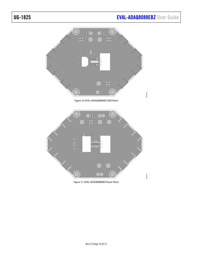
Figure 10. EVAL-ADAQ8088EBZ GND Plane
Figure 11. EVAL-ADAQ8088EBZ Power Plane
25
39
9-0
27
25
39
9-0
28
EVAL-ADAQ8088EBZ User Guide UG-1825
Rev. 0 | Page 11 of 12
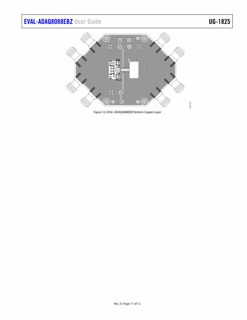
Figure 12. EVAL-ADAQ8088EBZ Bottom Copper Layer
25
39
9-0
29
UG-1825 EVAL-ADAQ8088EBZ User Guide
Rev. 0 | Page 12 of 12
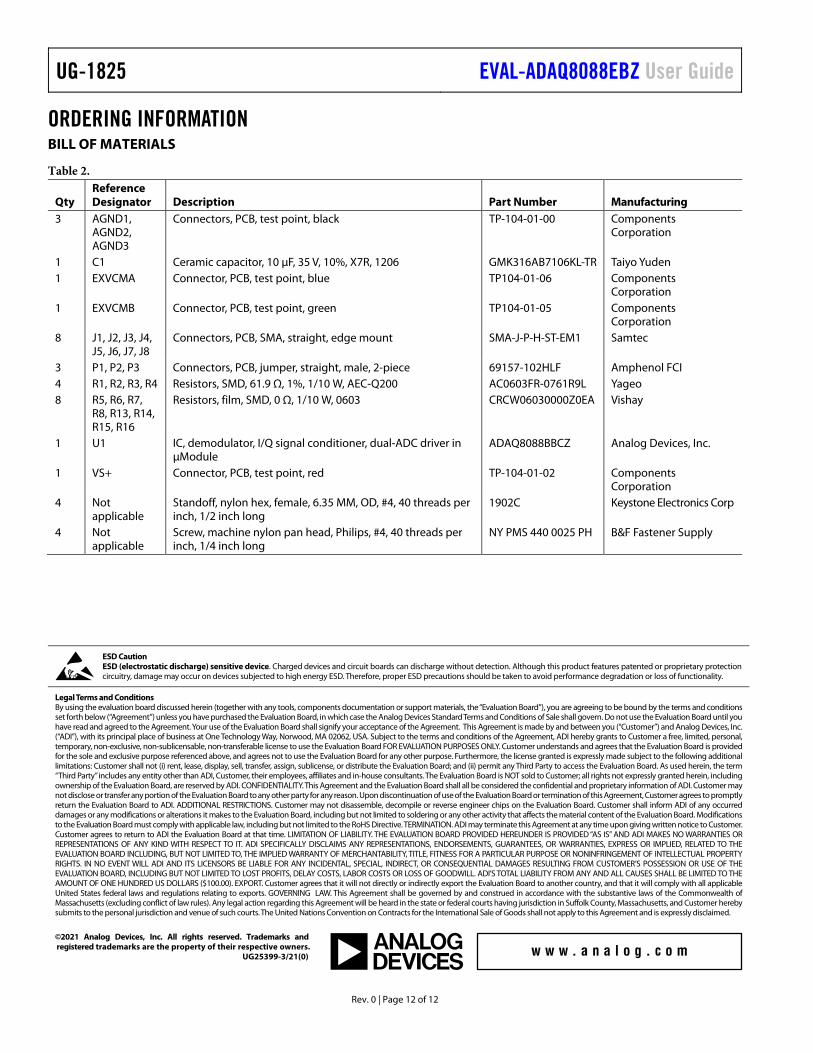
ORDERING INFORMATION BILL OF MATERIALS
Table 2.
Qty Reference Designator Description Part Number Manufacturing
3 AGND1, AGND2, AGND3
Connectors, PCB, test point, black TP-104-01-00 Components Corporation
1 C1 Ceramic capacitor, 10 μF, 35 V, 10%, X7R, 1206 GMK316AB7106KL-TR Taiyo Yuden 1 EXVCMA Connector, PCB, test point, blue TP104-01-06 Components
Corporation 1 EXVCMB Connector, PCB, test point, green TP104-01-05 Components
Corporation 8 J1, J2, J3, J4,
J5, J6, J7, J8 Connectors, PCB, SMA, straight, edge mount SMA-J-P-H-ST-EM1 Samtec
3 P1, P2, P3 Connectors, PCB, jumper, straight, male, 2-piece 69157-102HLF Amphenol FCI 4 R1, R2, R3, R4 Resistors, SMD, 61.9 Ω, 1%, 1/10 W, AEC-Q200 AC0603FR-0761R9L Yageo 8 R5, R6, R7,
R8, R13, R14, R15, R16
Resistors, film, SMD, 0 Ω, 1/10 W, 0603 CRCW06030000Z0EA Vishay
1 U1 IC, demodulator, I/Q signal conditioner, dual-ADC driver in μModule
ADAQ8088BBCZ Analog Devices, Inc.
1 VS+ Connector, PCB, test point, red TP-104-01-02 Components Corporation
4 Not applicable
Standoff, nylon hex, female, 6.35 MM, OD, #4, 40 threads per inch, 1/2 inch long
1902C Keystone Electronics Corp
4 Not applicable
Screw, machine nylon pan head, Philips, #4, 40 threads per inch, 1/4 inch long
NY PMS 440 0025 PH B&F Fastener Supply
ESD Caution ESD (electrostatic discharge) sensitive device. Charged devices and circuit boards can discharge without detection. Although this product features patented or proprietary protection circuitry, damage may occur on devices subjected to high energy ESD. Therefore, proper ESD precautions should be taken to avoid performance degradation or loss of functionality.
Legal Terms and Conditions By using the evaluation board discussed herein (together with any tools, components documentation or support materials, the “Evaluation Board”), you are agreeing to be bound by the terms and conditions set forth below (“Agreement”) unless you have purchased the Evaluation Board, in which case the Analog Devices Standard Terms and Conditions of Sale shall govern. Do not use the Evaluation Board until you have read and agreed to the Agreement. Your use of the Evaluation Board shall signify your acceptance of the Agreement. This Agreement is made by and between you (“Customer”) and Analog Devices, Inc. (“ADI”), with its principal place of business at One Technology Way, Norwood, MA 02062, USA. Subject to the terms and conditions of the Agreement, ADI hereby grants to Customer a free, limited, personal, temporary, non-exclusive, non-sublicensable, non-transferable license to use the Evaluation Board FOR EVALUATION PURPOSES ONLY. Customer understands and agrees that the Evaluation Board is provided for the sole and exclusive purpose referenced above, and agrees not to use the Evaluation Board for any other purpose. Furthermore, the license granted is expressly made subject to the following additional limitations: Customer shall not (i) rent, lease, display, sell, transfer, assign, sublicense, or distribute the Evaluation Board; and (ii) permit any Third Party to access the Evaluation Board. As used herein, the term “Third Party” includes any entity other than ADI, Customer, their employees, affiliates and in-house consultants. The Evaluation Board is NOT sold to Customer; all rights not expressly granted herein, including ownership of the Evaluation Board, are reserved by ADI. CONFIDENTIALITY. This Agreement and the Evaluation Board shall all be considered the confidential and proprietary information of ADI. Customer may not disclose or transfer any portion of the Evaluation Board to any other party for any reason. Upon discontinuation of use of the Evaluation Board or termination of this Agreement, Customer agrees to promptly return the Evaluation Board to ADI. ADDITIONAL RESTRICTIONS. Customer may not disassemble, decompile or reverse engineer chips on the Evaluation Board. Customer shall inform ADI of any occurred damages or any modifications or alterations it makes to the Evaluation Board, including but not limited to soldering or any other activity that affects the material content of the Evaluation Board. Modifications to the Evaluation Board must comply with applicable law, including but not limited to the RoHS Directive. TERMINATION. ADI may terminate this Agreement at any time upon giving written notice to Customer. Customer agrees to return to ADI the Evaluation Board at that time. LIMITATION OF LIABILITY. THE EVALUATION BOARD PROVIDED HEREUNDER IS PROVIDED “AS IS” AND ADI MAKES NO WARRANTIES OR REPRESENTATIONS OF ANY KIND WITH RESPECT TO IT. ADI SPECIFICALLY DISCLAIMS ANY REPRESENTATIONS, ENDORSEMENTS, GUARANTEES, OR WARRANTIES, EXPRESS OR IMPLIED, RELATED TO THE EVALUATION BOARD INCLUDING, BUT NOT LIMITED TO, THE IMPLIED WARRANTY OF MERCHANTABILITY, TITLE, FITNESS FOR A PARTICULAR PURPOSE OR NONINFRINGEMENT OF INTELLECTUAL PROPERTY RIGHTS. IN NO EVENT WILL ADI AND ITS LICENSORS BE LIABLE FOR ANY INCIDENTAL, SPECIAL, INDIRECT, OR CONSEQUENTIAL DAMAGES RESULTING FROM CUSTOMER’S POSSESSION OR USE OF THE EVALUATION BOARD, INCLUDING BUT NOT LIMITED TO LOST PROFITS, DELAY COSTS, LABOR COSTS OR LOSS OF GOODWILL. ADI’S TOTAL LIABILITY FROM ANY AND ALL CAUSES SHALL BE LIMITED TO THE AMOUNT OF ONE HUNDRED US DOLLARS ($100.00). EXPORT. Customer agrees that it will not directly or indirectly export the Evaluation Board to another country, and that it will comply with all applicable United States federal laws and regulations relating to exports. GOVERNING LAW. This Agreement shall be governed by and construed in accordance with the substantive laws of the Commonwealth of Massachusetts (excluding conflict of law rules). Any legal action regarding this Agreement will be heard in the state or federal courts having jurisdiction in Suffolk County, Massachusetts, and Customer hereby submits to the personal jurisdiction and venue of such courts. The United Nations Convention on Contracts for the International Sale of Goods shall not apply to this Agreement and is expressly disclaimed.
©2021 Analog Devices, Inc. All rights reserved. Trademarks and registered trademarks are the property of their respective owners. UG25399-3/21(0)
Mouser Electronics
Authorized Distributor
Click to View Pricing, Inventory, Delivery & Lifecycle Information: Analog Devices Inc.:
EVAL-ADAQ8088EBZ


