Embed Size (px)
Citation preview

Contents lists available at ScienceDirect
Materials Science in Semiconductor Processing
Materials Science in Semiconductor Processing 30 (2015) 62–74
http://d1369-80
n CorrE-m1 Cu
Californ2 Cu
3340043 Cu
New De
journal homepage: www.elsevier.com/locate/mssp
Evolution of surface morphology of alloyed AuGe/Ni/Au ohmiccontacts to GaAs microwave FETs
G. Sai Saravanan a,n, K. Mahadeva Bhat a, S. Dhamodaran b,1, A.P. Pathak b,R. Muralidharan c, H.P. Vyas c,2, D.V. Sridhara Rao d, R. Balamuralikrishnan d,K. Muraleedharan d,3
a Gallium Arsenide Enabling Technology Centre, Vignyanakancha P.O., Hyderabad-500069, Indiab School of Physics, University of Hyderabad, Central University P.O., Hyderabad-500046, Indiac Solid State Physics Laboratory, Timarpur, Delhi-110054, Indiad Defence Metallurgical Research Laboratory, Kanchanbagh, Hyderabad-500058, India
a r t i c l e i n f o
Keywords:AuGe/Ni/Au ohmic contactspHEMTMESFETSurface roughnessAFMElectron microscopy
x.doi.org/10.1016/j.mssp.2014.09.04101/& 2014 Elsevier Ltd. All rights reserved.
esponding author.ail address: [email protected] (G. Sairrently with Department of NanoEngineia San Diego, CA 92093, USArrently with Bikaner Technical University,, Indiarrently with Directorate of Materials, DRDOlhi-110001, India
a b s t r a c t
During post-deposition alloying of AuGe/Ni/Au ohmic contacts to microwave transistors,there is interdiffusion of alloy materials and GaAs into each other. Outdiffusion fromsubstrate greatly influences the surface roughness of the contacts as a function of alloyingtemperature. During our experiments, we have observed that the RMS roughness of thecontact surface followed the trend of contact resistance with alloying temperature. Weseek to explain this evolution of surface morphology using a model involving thephenomena of coalescence and outdiffusion occurring simultaneously.
& 2014 Elsevier Ltd. All rights reserved.
1. Introduction
Field effect transistors like High Electron MobilityTransistors (HEMTs) and MEtal Semiconductor Field EffectTransistors (MESFETs) are used as active devices in GaAs-based Monolithic Microwave Integrated Circuits (MMICs).The source and drain ohmic contacts to these devicesshould necessarily possess very low contact resistances(Rc) to allow efficient flow of current through the device inorder to effectively transfer or condition electrical signals.Low-resistance ohmic contact formation leads to high
Saravanan).ering, University of
Bikaner, Rajasthan-
Bhawan, Rajaji Marg,
source-drain currents (Idss), low saturation (Vsat) and knee(Vknee) voltages, and high transconductances (gm), whichare necessary for optimum and satisfactory device perfor-mances. This also results in lower voltage drops across thedevice during ON-state, and improves noise figure due tolower parasitic source resistances (Rs) [1].
As-deposited metallization on n-GaAs readily formsrectifying contacts due to differences in work function.Formation of ohmic contacts requires heat treatment aftermetal deposition (generally called alloying), in order todope the metal-nþ-GaAs (metal–semiconductor or M/S)interface and the sub-surface active layers, reducing theeffect of the M/S barrier at the interface. AuGe/Ni metalli-zation, consisting of low-melting (�360 1C) eutectic AuGe(12% Ge by wt.), has been widely used to form ohmiccontacts to n-GaAs devices [2,3]. During alloying, compo-nents of both the ohmic metal (Au, Ge and Ni) and thesemiconductor (Ga and As) diffuse into each other. Au,diffusing into the semiconductor, forms compounds likeAuGa within the active layers and creates vacancies of

Fig. 1. Schematics of (a) MESFET and (b) pHEMT device structures.
G. Sai Saravanan et al. / Materials Science in Semiconductor Processing 30 (2015) 62–74 63
gallium (VGa). Ge, while filling these vacancies, heavilydopes the semiconductor interface and the immediatesub-surface layers below the contact pads [4–7]. As aresult, various compounds of the type Ni2GeAs, NiAs2,NiGe, etc., are formed in the active layers below thecontact pads [4–6]. Similarly, the anions and cations fromthe semiconductor also simultaneously outdiffuse into thetop metallization, and form compounds such as AuGa inthe metal layers. Increasing arsenic outdiffusion, at veryhigh alloying temperatures, also leads to compensationand larger increase in Rc values [8,9].
The contact surface also undergoes visible morphologi-cal changes due to the heat treatment, which invariablymakes the ohmic contact surface rough. Contacts formedwith high surface roughness makes subsequent fabricationprocesses difficult (e.g., gate electrode formation and inter-connect formation in MMICs). Gate electrode of the tran-sistor, typically fabricated subsequent to ohmic contactformation, is formed in the gap between the source anddrain contacts, and often placed towards the source elec-trode. The typical gate dimensions, using optical lithogra-phy, are 0.5 mm, and, using electron beam lithography, aredown to 0.1 mm or even less. Gate electrodes are usuallyplaced in a gap of 4 mm to 2 mm between the source anddrain. Alignment marks, formed for lithography alignmentsof masks of one level with subsequent levels, are usuallyformed on the wafer in the initial stages of MMIC fabrica-tion. These are fabricated normally using ohmic metallayers, and formed simultaneously during the source-drainpad metallization step. When the ohmic contact surfacesare very rough, accurate alignment of the gate mask for0.5 mm gates, or gate pad mask for connecting the even
smaller gates becomes extremely difficult, often leading tomisaligned gates [10,11]. Accurate placement of the gate,therefore, becomes critical in these limited tolerances sinceit affects various device parameters like transconductanceand reverse breakdown voltage. Interconnect metal, con-necting the source-drain contact pads to other deviceelements, also serves as microwave transmission lines inMMICs. High roughness of contact surface increases theresistance between the interconnect metallization and thedevice contact pads, and often causes current crowding.Contact pad roughness also affects the definition of padedges, invariably resulting in poor device performances.Hence, low resistance ohmic contacts with less roughnessand acceptable morphology are highly desirable.
Therefore, while optimizing the contact resistance ofthe devices, efforts were also made to study and minimizesurface roughness. We report the studies on the morphol-ogy of AuGe/Ni/Au ohmic contacts to pseudomorphicHEMTs (pHEMTs) and MESFETs, alloyed at different tem-peratures. We have observed that the trend of RMS rough-ness values of the contact surface followed the trend ofcontact resistance with alloying temperature, and thetrend is similar for both pHEMT and MESFET samples.
2. Experimental details
The active layers of MESFET (Fig. 1a) were ion-implantedwith Si29þ into semi-insulating GaAs followed by rapidthermal annealing for activation [12]. The carrier concen-trations of nþ-GaAs contact and n-GaAs channel layerswere 2–3�1018 cm�3 and 2–3�1017 cm�3, respectively.The typical layer thicknesses were about 0.15 μm and0.35 μm, respectively. The typical pHEMT structure, grownby molecular beam epitaxy (MBE) technique, is shown inFig. 1b. The thickness of different layers were as follows:superlattice buffer, consisting of 10 periods of alternatelayers of undoped AlxGa1�xAs and undoped GaAs, eachwith a thickness of 50 Å, semi-insulating GaAs buffer layer(5000 Å), InxGa1�xAs channel (120 Å), AlxGa1�xAs spacer(30 Å), a Si δ-doped layer, AlxGa1�xAs Schottky layer(250 Å), and finally an nþ-GaAs contact layer (500 Å) dopedto a concentration of 5�1018 cm�3 on the surface.
Mesas were formed by photolithography, and isolatedby wet chemical etching. AuGe, Ni and Au were thermallyevaporated to a thickness of 1000 Å, 300 Å and 3000 Å,respectively, and subsequently lifted off. Rapid thermalalloying experiments were carried out in a forming gasambience in an AET Thermal RXV6 Rapid Thermal Proces-sor (RTP), at temperatures from 380 1C to 420 1C, for theMESFET samples, and from 390 1C and 450 1C, for thepHEMT samples [13–15]. The purpose of these experi-ments was to study the morphology on wafers withdevices ultimately used for MMIC fabrication. Hence theaim was to achieve as reasonable morphology as possiblefor useful device applications. Therefore, these waferswere chosen to have the standard test structures of thetransfer length method (TLM) patterns as well as activedevices (pHEMTs and MESFETs), formed on the mesas[15,16]. While Rc was measured on TLM patterns, and DCparameters were measured on the test devices, the surface

Fig. 2. AFM surface scan images of MESFET samples alloyed at (a) 380 1C, (b) 400 1C and (c) 420 1C.
G. Sai Saravanan et al. / Materials Science in Semiconductor Processing 30 (2015) 62–7464
roughness experiments were carried out on both TLM padsas well as source-drain pads of the devices.
Surface morphology was characterized by atomic forcemicroscope (AFM) in the intermittent contact or dynamicforce mode (DFM) using SPA 400 of Seiko Instruments,Inc., and Leo 440i scanning electron microscope (SEM)with energy dispersive x-ray spectroscopy (EDS). Contactswere further investigated by cross-section transmissionelectron microscopy (TEM, XTEM) using a Tecnai 20 Tanalytical TEM, operated at 200 kV, and equipped withan EDS SUTW detector (EDAX, USA). The specimens forXTEM were prepared to electron-transparent thickness[18]. A low-background double-tilt specimen holder wasused during XTEM studies. In addition, to understand thenature of the ‘reacted’ semiconductor region under theohmic pads after alloying, the metallization of the alloyedsamples was etched subsequently in standard KI and I2-based gold etchant [17], and samples studied by SEM.
3. Results
The lowest Rc value of 0.04Ω-mm was obtained forMEFSETs at 400 1C. The typical contact resistances were about0.05–0.07Ω-mm (referred to here as ‘optimally alloyed’)
[13,14]. In the case of pHEMTs, the lowest Rc value of0.0475Ω-mmwas obtained for alloying at 430 1C. The typicalcontact resistances were about 0.05–0.07Ω-mm (optimallyalloyed) [15].
Alloying at temperatures below and above the optimalalloying temperatures resulted in ‘under-alloyed’ and‘over-alloyed’ contacts, respectively, and Rc values werehigh in both the cases.
Fig. 2 shows the AFM images of the ohmic contact padsof MESFET samples alloyed at 380 1C, 400 1C and 420 1C.The scan area in all the samples was 3 μm � 3 μm. Theindicative surface roughness across each sample surface isshown as line profiles in Fig. 3. While the 380 1C-alloyedsample showed higher local variations of roughness, the420 1C-alloyed showed the presence of large blister-likeprotrusions in the contact metallization. The optimallyalloyed sample, however, had a smoother surface withuniform features. The lowest RMS roughness was obtainedfor the 400 1C-alloyed sample (Fig. 4), and the RMS rough-ness values were higher for the ‘under-alloyed’ as well asthe ‘over-alloyed’ samples. The trend of variation of RMSroughness as a function of alloy temperature is shownalongwith the graph showing variation of contact resistanceas a function of alloy temperature of MESFET samples, in
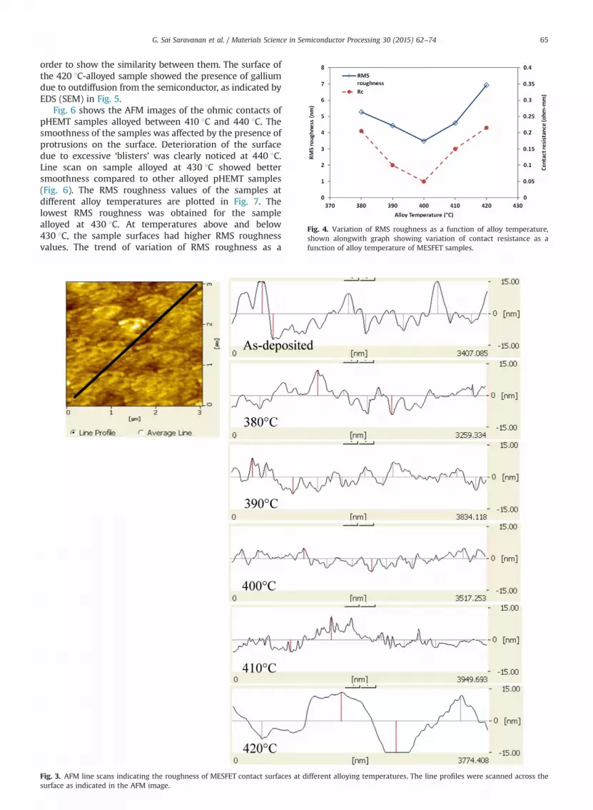
Fig. 4. Variation of RMS roughness as a function of alloy temperature,shown alongwith graph showing variation of contact resistance as afunction of alloy temperature of MESFET samples.
G. Sai Saravanan et al. / Materials Science in Semiconductor Processing 30 (2015) 62–74 65
order to show the similarity between them. The surface ofthe 420 1C-alloyed sample showed the presence of galliumdue to outdiffusion from the semiconductor, as indicated byEDS (SEM) in Fig. 5.
Fig. 6 shows the AFM images of the ohmic contacts ofpHEMT samples alloyed between 410 1C and 440 1C. Thesmoothness of the samples was affected by the presence ofprotrusions on the surface. Deterioration of the surfacedue to excessive ‘blisters’ was clearly noticed at 440 1C.Line scan on sample alloyed at 430 1C showed bettersmoothness compared to other alloyed pHEMT samples(Fig. 6). The RMS roughness values of the samples atdifferent alloy temperatures are plotted in Fig. 7. Thelowest RMS roughness was obtained for the samplealloyed at 430 1C. At temperatures above and below430 1C, the sample surfaces had higher RMS roughnessvalues. The trend of variation of RMS roughness as a
Fig. 3. AFM line scans indicating the roughness of MESFET contact surfaces at different alloying temperatures. The line profiles were scanned across thesurface as indicated in the AFM image.

Fig. 5. EDS (SEM) spectrum of the surface of MESFET sample alloyed at 420 1C showing out-diffusion of gallium.
Fig. 6. AFM line scans of the contact surfaces along with images of pHEMT samples alloyed at 410 1C, 430 1C and 440 1C.
G. Sai Saravanan et al. / Materials Science in Semiconductor Processing 30 (2015) 62–7466
function of alloy temperature is shown alongwith thegraph showing variation of contact resistance as a functionof alloy temperature of pHEMT samples, in order to showthe similarity between them. This trend of RMS roughnessis also similar to that observed in the case of MESFETs.
In order to understand the surface beneath the alloyedmetallization, the metal pads in the above samples were
etched away. After this etching, the semiconductor sur-faces revealed the ‘reacted’ semiconductor underneath dueto alloying. Fig. 8a shows the smoothness of the ‘reacted’semiconductor surface of the MESFET sample alloyed at400 1C with larger features. The local variations of rough-ness within such a feature and across such features werevery minimal. In contrast, the 390 1C-alloyed sample had

G. Sai Saravanan et al. / Materials Science in Semiconductor Processing 30 (2015) 62–74 67
smaller features with distinctly varying heights and depthsacross the sample (Fig. 8b), and the 420 1C-alloyed samplehad large undulations with varying feature sizes (Fig. 8c).Similarly, in pHEMT samples, the ‘reacted’ surface patternson the ‘under-alloyed’ (410 1C) contacts, with varying
Fig. 7. Variation of RMS roughness as a function of alloy temperature,shown alongwith graph showing variation of contact resistance as afunction of alloy temperature of pHEMT samples.
Pad area
Fig. 8. SEM pictures of the etched surfaces of MESFETs under the contact pads400 1C, (b) 390 1C sample showing local variations and rough surface, and (c) R
feature sizes (Fig. 9a), and ‘over-alloyed’ (440 1C) (Fig. 9b)contacts, with large features with different sizes and arough morphology, showed large amounts of roughness.The 430 1C-alloyed sample was less rough compared to theother samples (Fig. 9c), and had uniform feature sizes withless height variations.
The XTEM image of as-deposited sample (Fig. 10a)shows the surface roughness of the top gold layer. Fig. 10bshows a higher magnification of the surface of the samemetal layer revealing the presence of smaller grains of gold.The microdiffraction pattern (XTEM) obtained from thesegrains is indexed, as shown in Fig. 11, and the indexed ‘d-spacings’ matched that of gold (Table 1) [19]. To establish acomparison of the alloyed surfaces with the as-depositedsurface, the alloyed MESFET samples were first examined byXTEM. Fig. 12a shows the formation of smaller columnargrains of gold at the surface of the sample alloyed at 390 1C.Fig. 12b shows the formation of large-sized gold grains atthe surface of the 400 1C-alloyed sample with very lowsurface roughness. In the 420 1C-alloyed sample, the goldgrains were seen further elongated in shape (Fig. 12c), withthe presence of blister-like protrusions (Fig. 12d). EDSanalysis was performed on these XTEM samples in TEM,
revealing the ‘reacted’ GaAs. (a) Smooth surface of the wafer alloyed atough surface of the wafer alloyed at 420 1C.

Fig. 9. Etched surfaces under the contact pads revealing the amount of roughness of the ‘reacted’ GaAs in (a) ‘Under-alloy’, (b) ‘Over-alloy’ and (c) Optimumalloy pHEMT samples.
BF
Top surface
Top surface
BF
Fig. 10. XTEM images of as-deposited sample showing (a) roughness of contact surface and (b) smaller gold grains at a higher magnification.
G. Sai Saravanan et al. / Materials Science in Semiconductor Processing 30 (2015) 62–7468
on the gold grains as well as inside the protruded blisters.This revealed the presence of arsenic and gallium (Fig. 13).
Similar to MESFETs, cross-section images of the alloyedpHEMT samples were studied next. Fig. 14a shows thebright field (BF) XTEM image of the surface morphologyof the 410 1C-alloyed pHEMT sample with gold-rich grains.Fig. 14b shows a smoother surface with gold-rich grains ofthe 430 1C-alloyed sample, with small protrusions (Fig. 14c),
but their sizes were smaller compared to the ‘under-alloyed’sample and density lesser. Whereas, the Au-rich grain sizeswere coarser and larger in the ‘over-alloyed’ sample, withlarge protrusions due to outdiffusion (Fig. 14d).
EDS (SEM) spectra from the overlayer Au of the abovepHEMT samples are shown in Fig. 15. A gradual increase inthe outdiffusion of Ga is observed with temperature. Alongwith Ga, the sample alloyed at 440 1C shows the presence

Fig. 11. XTEM microdiffraction pattern from the gold grains indexed.
Table 1Indexed ‘d-spacings’ of gold grains in the as-deposited metal.
No. d experimental (Å) d theoretical (Å)
1 2.361 2.3552 2.045 2.0393 1.441 1.4424 1.234 1.2305 1.174 1.1776 0.932 0.9367 0.788 0.785
D
Top surface
BF
Top surface
DF
Fig. 12. XTEM images of MESFET (a) sample alloyed at 390 1C showing smaller ggrains of gold formed at the surface, respectively, and (d) 420 1C sample surface
G. Sai Saravanan et al. / Materials Science in Semiconductor Processing 30 (2015) 62–74 69
of As also. The ‘blister’ region on this sample can be seenwith even higher amounts of Ga outdiffusion. In order toconfirm the presence of these outdiffused elements, EDSanalysis was performed on the XTEM samples in TEM, onthe gold grains as well as inside the protruded blisters.This revealed the presence of arsenic and gallium, espe-cially higher levels inside the protrusion (Fig. 16). Micro-diffraction pattern, also obtained on these gold-rich grainson the XTEM samples in TEM, was indexed (Fig. 17), andthe indexed ‘d-spacings’ matched nearest to the com-pound of AuGa confirming the presence of Ga as a resultof outdiffusion in the top metallization (Table 2) [19].
4. Discussion
The basic requirement of ohmic contact alloying aftermetallization is to enable diffusion of alloy materials acrossthe barrier at metal-nþ–GaAs interface. In particular, diffu-sion of germanium is necessary for increasing the level ofdoping at the interface and the immediate sub-surface devicelayers in order to reduce the effect of the barrier. Duringalloying, Au also diffuses into the semiconductor formingcompounds with Ga, leading to the creation of Ga vacancies.The inward diffusing Ge and Ni form compounds with As,doping the semiconductor at the Ga vacancies, and, heavy Gedoping reduces the contact resistances [15,18,20–22]. WhileNi- and Ge-rich compounds were found dominant anduniformly present in the diffusion regions in the optimally
Top surface
F
Top surface
BF
old grains, (b) and (c) samples alloyed at 400 1C and 420 1C, showing largewith ‘blister’.

Fig. 13. a. EDS (XTEM) at metal surface. Fig. 13b. EDS (XTEM) at center of protrusion on surface. Fig. 13c. EDS (XTEM) at top portion of protrusion on surface.
G. Sai Saravanan et al. / Materials Science in Semiconductor Processing 30 (2015) 62–7470
alloyed samples, Au-rich compounds were observed to bedominant in ‘under-alloy’ and ‘over-alloy’ samples [14,15,18].It is possible that the templates of the ‘reacted’ semiconductor
surfaces, revealed after the removal of the ohmic metal padsby etching, probably point to the nature and uniformity offormation of such Ni-rich or Au-rich compounds, leading to

BF
Top surface
Top surface
BF
BF
Top surface
Protrusion
Top surface
BF
Protrusion
Fig. 14. XTEM images of pHEMT samples of (a) ‘Under-alloy’ with smaller gold grains, (b) 430 1C with large grains, (c) ‘Over-alloy’ with larger grains andprotrusion, and (d) ‘Over-alloy’ with a large protrusion.
G. Sai Saravanan et al. / Materials Science in Semiconductor Processing 30 (2015) 62–74 71
either very low and uniform Rc as well as RMS roughnessvalues, or the lack of such values. During the occurrence ofinward diffusion, compounds like AuGa are also formed inthe metal over-layers, almost simultaneously, owing to out-diffusion from the substrate [23–25]. It is expected that as thealloying temperature is increased, outdiffusion of Ga and Astoo increases, which should have led to increasing surfaceroughness [24]. Instead, we observed two different behaviors:a trend of decreasing roughness as we proceeded towardsoptimal alloy temperatures, and, an increasing roughnessabove optimal alloy temperatures.
Achievement of very low Rc values for typical MESFETstructures was possible at lower alloy temperatures suchas 400 1C, as these structures consist of only GaAs layers.Whereas, since pHEMT structures possess higher band gapAlGaAs layers, they pose a barrier to the diffusion of alloymaterials, requiring higher alloy temperatures to achievelow Rc values [22,26–28].
It is seen that the as-deposited film consists of smallgrains formed during deposition (Fig. 10b). When themetallization is subjected to alloying temperatures, coa-lescence is initiated. The driving force for coalescence is tomaintain a minimum overall surface area of the grains. It isknown that in metals such as Al, Ag, Au and Cu, the highersurface mobility of the adatoms leads to continued
structure evolution of the metallization [29]. The surfacemorphology alters due to the fact that grain growthcontinues to occur during the post-deposition heat treat-ments (like contact alloying, in this case). After the onset ofgrain growth, the average size of the grains increases. Thesurface begins to smoothen due to formation of columnargrains, separated by grain boundaries [30]. Grains growfurther in size with increasing temperature leading toequiaxial grain formation, eventually resulting in reduc-tion in the number of grains, for example, as revealed byXTEM images in Fig. 12 (a and b). This activity ceases whenthe grain sizes become comparable to the film thickness.The morphology evolution process is pictorially depictedin Fig. 18, with the transition from surface smoothening tosurface roughening shown occurring near 400 1C for thecase of MESFETs. In the case of ohmic contact alloying of n-GaAs-based microwave devices, this smoothening processis interfered by the increasing outdiffusion as alloy tem-peratures are increased. The reduction of roughness of theas-deposited ohmic metallization proceeds until the opti-mum alloying temperature, and outdiffusion processbecomes dominant above this temperature. The processof smoothening would have continued beyond the optimalalloy temperature but for the increasing outdiffusion thatmasks the effect, resulting in the onset of roughening of

Fig. 15. EDS (SEM) spectra from the overlayers of pHEMT samples of (a) ‘Under-alloy’, (b) 430 1C, (c) ‘Over-alloy’ and (d) ‘Over-alloy’ ‘blister’.
G. Sai Saravanan et al. / Materials Science in Semiconductor Processing 30 (2015) 62–7472
the surface. As the active layers of both MESFET andpHEMT contain large atomic percentage of gallium, andthe trend observed with respect to surface roughness, as a
function of alloying conditions, is similar for both pHEMTsamples and MESFET samples. The comparison is onlybetween the trends observed.

Fig. 16. a. EDS (XTEM) at center of protrusion on surface of pHEMT sample. Fig. 16b. EDS (XTEM) at top portion of protrusion on surface of pHEMT sample.Fig. 16c. EDS (XTEM) at gold grains on pHEMT sample.
G. Sai Saravanan et al. / Materials Science in Semiconductor Processing 30 (2015) 62–74 73

Fig. 17. Microdiffraction pattern obtained from the gold-rich grains indexed.
Table 2Indexed ‘d-spacings’ of gold-rich grains matching nearest to AuGacompounds.
No. d experimental (Å) d theoretical (Å)
1 2.622 2.6202 2.225 2.2303 2.203 2.2004 1.241 1.2405 1.245 1.240
2
3
4
5
6
7
8
370 380 390 400 410 420 430
RM
S ro
ughn
ess
(nm
)
Alloy temperature (°C)
> 400ºCAs-deposited
Substrate
< 400ºC400ºC
Fig. 18. Evolution of surface morphology of ohmic contacts. The transi-tion from surface smoothening to surface roughening occurs near 400 1Cfor MESFETs.
G. Sai Saravanan et al. / Materials Science in Semiconductor Processing 30 (2015) 62–7474
5. Conclusion
It was observed that the integrity of the surfacemorphology of AuGe/Ni/Au ohmic contacts to source anddrain electrodes of MESFETs and pHEMTs was preservedwhen they were optimally alloyed. The RMS roughness ofthe contact surface followed the trend of contact resis-tance with alloying temperature, and the contacts ofMESFETs and pHEMTs with the lowest RMS surface rough-ness values also had the lowest Rc. Low values of rough-ness indicate that the process window is large for theoptimum alloy cycle, and hence ensures stability of contactformation. We have attempted to interpret this using amodel wherein the phenomenon of coalescence leading tosmoother surface morphology dominates upto the optimalalloy temperatures, beyond which outdiffusion becomesoverriding, resulting in increase in roughness.
Acknowledgments
We thank the Fab team for help during fabrication and,Mr. M.N. Mudholkar and Dr. S.L. Badnikar for technicaldiscussions and permission to publish this work.
References
[1] P. O’Connor, A. Dori, M. Feuer, R. Vounckx, IEEE Trans. ElectronDevices 34 (4) (1987) 765–771.
[2] A.G. Baca, F. Ren, J.C. Zolper, R.D. Briggs, S.J. Pearton, Thin Solid Films308–309 (1997) 599–606.
[3] Masanori Murakami, Sci. Technol. Adv. Mater. 3 (2002) 1–27.[4] N. Braslau, J. Vac. Sci. Technol. 19 (3) (1981) 803–807.[5] A.K. Rai, A. Ezis, A.W. McCormick, A.K.P. Long, D.W. Langer, J. Appl.
Phys. 61 (9) (1987) 4682–4688.[6] N.E. Lumpkin, G.R. Lumpkin, Proc. Optoelectronic Microelectron.
Mater. Devices (1996) 341–344.[7] S.A. Schwarz, C.J. Palmstrom, C.L. Schwartz, T. Sands, L.G. Shantharama
J.P. Harbison, L.T. Florez, E.D. Marshall, C.C. Han, S.S. Lau, L.H. AllenJ.W. Mayer, J. Vac. Sci. Technol. A 8 (3) (1990) 2079–2083.
[8] J.R. Shappirio, R.T. Lareau, R.A. Lux, J.J. Finnegan, D.D. SmithL.S. Heath, M. T-Lara, J. Vac. Sci. Technol. A 5 (4) (1987) 1503–1507.
[9] A. Messica, U. Meirav, H. Shtrikman, Thin Solid Films 257 (1995) 54–57.[10] R.K. Ball, Thin Solid Films 176 (1989) 55–68.[11] J.A. Bardwell, S. Haffouz, H. Tang, R. Wang, J. Electrochem. Soc. 153 (8)
(2006) G746–G749.[12] G. Sai Saravanan, K. Mahadeva Bhat, H.P. Vyas, K. Muraleedharan
A.P. Pathak, Radiat. Eff. Defect Solids 163 (9) (2008) 737–748.[13] G. Sai Saravanan, K. Mahadeva Bhat, H.P. Vyas, Sandeep Chaturvedi,
Sangam V. Bhalke, R. Muralidharan, K. Muraleedharan and A.P.Pathak, Reliability studies of AuGe/Ni/Au ohmic contacts to MESFETsby accelerated thermal aging tests, in: Proceedings of the 14th IEEEInternational Workshop of Physics of Semiconductor Devices, Mum-bai, Dec 16–20, Ed. K. L. Narasimhan and D. K. Sharma ⟨www.ieeeexplore.ieee.org⟩. 2007, pp. 462–465.
[14] G. Sai Saravanan, K. Mahadeva Bhat., Sandeep Chaturvedi, M.N.Mudholkar, R. Muralidharan, Backside SIMS analysis and acceleratedthermal aging of optimally alloyed ohmic contacts to MESFETs, in:Proceedings of the CS MANTECH Conference, May 17–20, Portland,Oregon, USA, 2010, pp. 323–325.
[15] G. Sai Saravanan, K. Mahadeva Bhat, K. Muraleedharan, H.P. Vyas,R. Muralidharan, A.P. Pathak, Semicond. Sci. Technol. 23 (2008)501–506.
[16] Dieter K. Schroder, Semiconductor Material and Device Character-ization, first ed. John Wiley & Sons, Inc., Singapore, 1990.
[17] Ralph Williams, Modern GaAs Processing Methods, Second ed.Artech House, Boston, 1990.
[18] D.V. Sridhara Rao, G. Sai Saravanan, K. Muraleedharan,R. Balamuralikrishnan, R. Muralidharan, H.P. Vyas, Metals, Mater.Processes 19 (1–4) (2007) 171–180.
[19] M.F. Toney, in: C.R. Brundle, C.A. Evans Jr., S. Wilson (Eds.), Encyclo-pedia of Materials Characterization: Surfaces Interfaces, Thin Films,Butterworth-Heinmann, Stoneham, MA, USA, 1992, pp. 198–213.
[20] M.A. Crouch, S.S. Gill, J. Woodward, S.J. Courtney, G.M. WilliamsA.G. Cullis, Solid-State Electron. 33 (11) (1990) 1437–1446.
[21] T.K. Higman, M.A. Emanuel, J.J. Coleman, S.J. Jeng, C.M. WaymanJ. Appl. Phys. 60 (2) (1986) 677–680.
[22] J.–L. Lee, Y.–T. Kim, H.M. Yoo, G.Y. Lee, J. Vac. Sci. Technol. B 17 (3)(1999) 1034–1039.
[23] M. Ogawa, J. Appl. Phys. 51 (1) (1980) 406–412.[24] Masanori Murakami, K.D. Childs, J.M. Baker, A. Callegari, J. Vac. Sci.
Technol. B 4 (1986) 903.[25] C. Lin, C.P. Lee, J. Appl. Phys. 67 (1990) 260.[26] P. Zwicknagl, S.D. Mukherjee, P.M. Capani, H. Lee, H.T. Griem,
L. Rathbun, J.D. Berry, W.L. Jones, L.F. Eastman, J. Vac. Sci. Technol.B 4 (2) (1986) 476–484.
[27] H. Goronkin, S. Tehrani, T. Remmel, P.L. Fejes, K.J. Johnson, IEEETrans. Electron. Devices 36 (2) (1989) 281–288.
[28] Y. Jin, Solid-State Electron. 34 (2) (1991) 117–121.[29] L.B. Freund, S. Suresh, Thin Film Materials: Stress, Defect Formation and
Surface Evolution, first ed. Cambridge university press, Cambridge,2003.
[30] Subhash Mahajan, K.S. Sree Harsha, Principles of Growth andProcessing of Semiconductors, first ed. McGraw Hill, Boston, 1999.


