Embed Size (px)
Citation preview
IEEE JOURNAL OF SOLID-STATE CIRCUITS, VOL. 32, NO. 3, MARCH 1997 407
Forming DampedLRC Parasitic Circuits inSimultaneously Switched CMOS Output Buffers
Thaddeus J. Gabara,Member, IEEE, Wilhelm C. Fischer, John Harrington, and William W. Troutman
Abstract—Several techniques to reduce the ground bounceeffect in CMOS chips are described. The effective width ofthe predrive and final driver of a CMOS output buffer isautomatically adjusted to compensate for process, voltage, andtemperature (PVT) variations. The slew rate of the predrive nodesis controlled by introducing a digitally weighted capacitance.Finally, a compensated active resistance is inserted into both thepower and ground leads to further dampen the oscillations. Thesetechniques allow the buffer to behave uniformly over the entirePVT range. Measurements of a 0.5-�m CMOS test chip havedemonstrated that these new buffers generate 2.5� less groundbounce when compared to conventional buffers. An externalresistance is required to set a reference current.
Index Terms—Buffer circuits, noise.
I. INTRODUCTION
CMOS bus widths in IC packages have been increasingover the years. The bus width of several designs are ap-
proaching 128 b and even wider structures can be expected. Asthe technology continues to scale down, the IC’s performancehas and is being limited by the package and printed circuitboard (PCB) parasitic’s, i.e., inductance and capacitance.
Many of these wide bus structures are driven by singled-ended transistor-transistor logic (TTL) or full swing CMOSbuffers. Single-ended output complicates the ground bounceconcern since large current fluctuations can occur in the VDDor VSS power leads during simultaneous switching events.The voltage drop that is generated across these parasiticinductances is known as ground bounce [1]. Ideally, a balancedoutput circuit structure like emitter coupled logic (ECL), whichuses current steering to transfer data, helps to alleviate thisproblem since the current in the inductance remains constant.With no change in the current, the voltage drop across theinductance can approach zero. One difficulty in applying thismethod to CMOS designs is that additional power would bedissipated in the chip. Another critical concern would be theinput/output (I/O) pin count which is a premium commodity.The limited number of physical I/O pins of a chip must beshared among data, control, power, and ground leads. On manyIC’s, power and ground leads can consume up to 30–40% ofthe total I/O pin count in order to insure a low inductancepath to the power supplies which minimizes the ground bouncegeneration. It would be desirable to introduce techniques into
Manuscript received August 7, 1996; revised October 24, 1996.T. Gabara, W. C. Fischer, and W. W. Troutman are with Bell Laboratories,
Lucent Technologies, Murray Hill, NJ 07974 USA.J. Harrington is with Lucent Technologies, Allentown, PA 18103 USA.Publisher Item Identifier S 0018-9200(97)01256-0.
the output buffer and associated circuitry which will allow areduction of the power and ground leads. This would allowthe packaging of a device into a smaller pin count packagewhich would reduce the board area and the cost of the IC.
The situation is further complicated by the external condi-tions that can be applied to the CMOS circuit, i.e., process,voltage, and temperature (PVT) variations. The three-sigmaspread of these variables makes it difficult to determine thenumber of power and ground leads required in the package. Itwould be desirable to determine the effect of ground bouncein a more predictable manner. The solution is to use dynamiccircuit sizing which compensates the adverse effect of PVTvariations on circuit performance.
This paper will describe the source of the ground bounceproblem and introduce circuit techniques which control itsgeneration [2]. Measurement results of a 0.5-m test chipusing these techniques will be given.
II. SOURCE OF PROBLEM
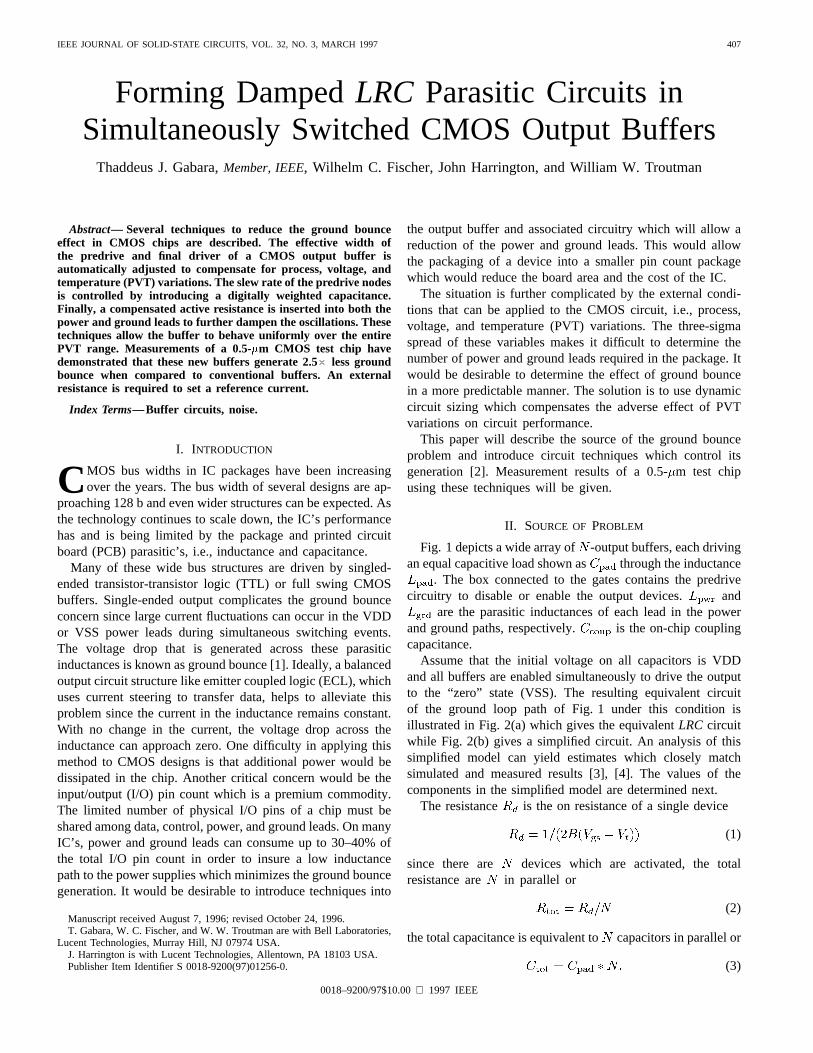
Fig. 1 depicts a wide array of -output buffers, each drivingan equal capacitive load shown as through the inductance
. The box connected to the gates contains the predrivecircuitry to disable or enable the output devices. and
are the parasitic inductances of each lead in the powerand ground paths, respectively. is the on-chip couplingcapacitance.
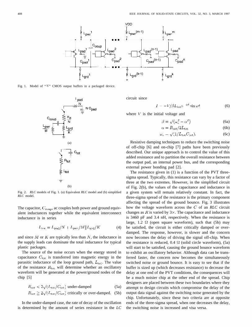
Assume that the initial voltage on all capacitors is VDDand all buffers are enabled simultaneously to drive the outputto the “zero” state (VSS). The resulting equivalent circuitof the ground loop path of Fig. 1 under this condition isillustrated in Fig. 2(a) which gives the equivalentLRC circuitwhile Fig. 2(b) gives a simplified circuit. An analysis of thissimplified model can yield estimates which closely matchsimulated and measured results [3], [4]. The values of thecomponents in the simplified model are determined next.
The resistance is the on resistance of a single device
(1)
since there are devices which are activated, the totalresistance are in parallel or
(2)
the total capacitance is equivalent tocapacitors in parallel or
(3)
0018–9200/97$10.00 1997 IEEE
408 IEEE JOURNAL OF SOLID-STATE CIRCUITS, VOL. 32, NO. 3, MARCH 1997
Fig. 1. Model of “N ” CMOS output buffers in a packaged device.
(a)
(b)
Fig. 2. RLC models of Fig. 1. (a) EquivalentRLC model and (b) simplifiedRLC model.
The capacitor, , ac couples both power and ground equiv-alent inductances together while the equivalent interconnectinductance is in series
(4)
and since or are typically less than , the inductance inthe supply leads can dominate the total inductance for typicalplastic packages.
The source of the noise occurs when the energy stored incapacitance is transferred into magnetic energy in theparasitic inductance of the loop ground path, . The valueof the resistance will determine whether an oscillatorywaveform will be generated at the power/ground nodes of thechip [5]
under-damped (5a)
critically or over-damped. (5b)
In the under-damped case, the rate of decay of the oscillationis determined by the amount of series resistance in theLC
circuit since
(6)
where is the initial voltage and
(6a)
(6b)
(6c)
Resistive damping techniques to reduce the switching noiseof off-chip [6] and on-chip [7] paths have been previouslydescribed. Our unique approach is to control the value of thisadded resistance and to partition the overall resistance betweenthe output pad, an internal power bus, and the correspondingexternal power bonding pad [2].
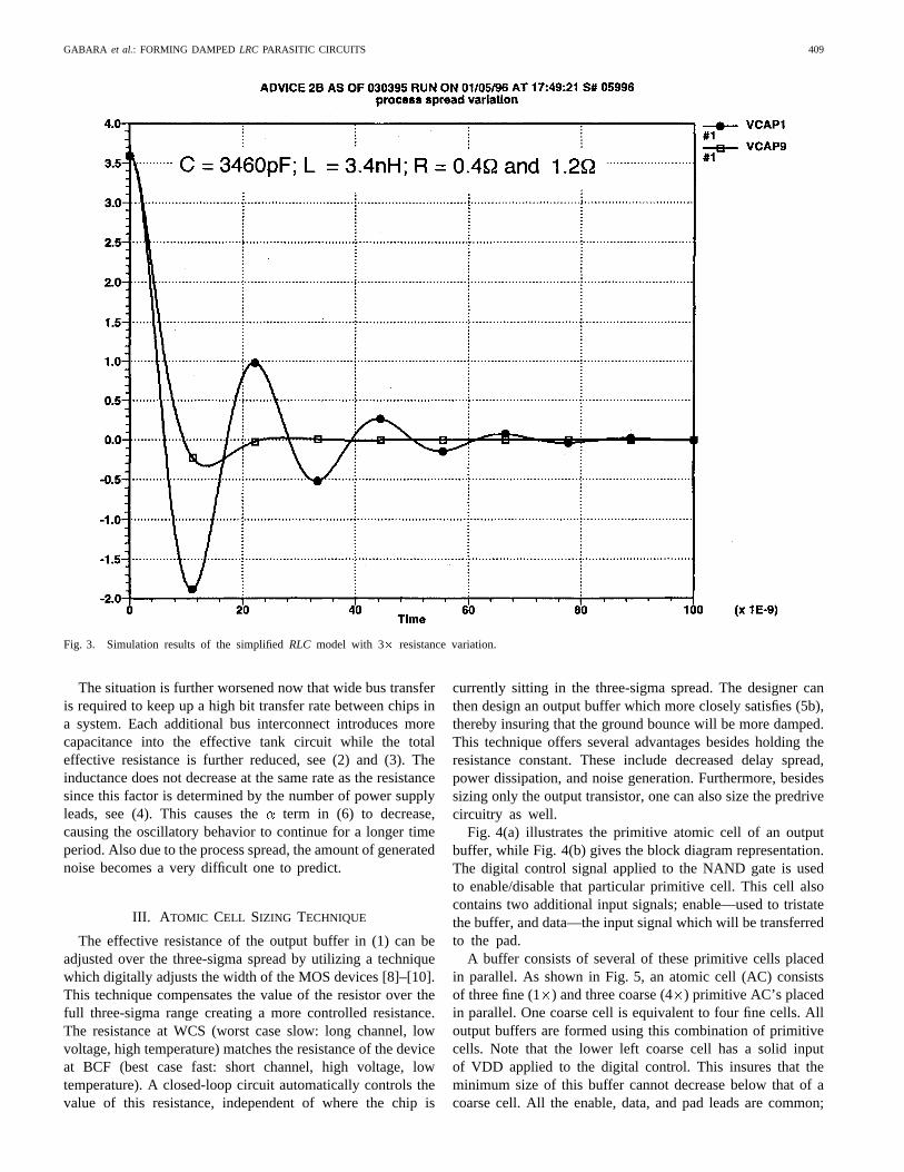
The resistance given in (1) is a function of the PVT three-sigma spread. Typically, this resistance can vary by a factor ofthree at the two extremes. However, in the simplified circuitof Fig. 2(b), the values of the capacitance and inductance ina given system will remain relatively constant. In fact, thethree-sigma spread of the resistance is the primary componentaffecting the spread of the ground bounce. Fig. 3 illustrateshow the voltage waveform across the of an RLC circuitchanges as is varied by 3 . The capacitance and inductanceis 3460 pF and 3.4 nH, respectively. When the resistance islarge, 1.2 (open square waveform), such that (5b) maybe satisfied, the circuit is either critically damped or over-damped. The response, however, is slower and the concernnow becomes the delay of driving the signal off-chip. Whenthe resistance is reduced, 0.4(solid circle waveform), (5a)will start to be satisfied, causing the ground bounce waveformto exhibit an oscillatory behavior. Although data can be trans-ferred faster, the concern now becomes the simultaneouslyswitched noise or ground bounce. It is easy to see that if thebuffer is sized up (which decreases resistance) to decrease thedelay at one end of the PVT conditions, the consequences willbe a much noisier chip at the other end of the spread. Chipdesigners are placed between these two boundaries where theyattempt to design circuits which compromise the delay of theoutput data signal against the switching noise generated by thechip. Unfortunately, since these two criteria are at oppositeends of the three-sigma spread, when one decreases the delay,the switching noise is increased and visa versa.
GABARA et al.: FORMING DAMPED LRC PARASITIC CIRCUITS 409
Fig. 3. Simulation results of the simplifiedRLC model with 3� resistance variation.
The situation is further worsened now that wide bus transferis required to keep up a high bit transfer rate between chips ina system. Each additional bus interconnect introduces morecapacitance into the effective tank circuit while the totaleffective resistance is further reduced, see (2) and (3). Theinductance does not decrease at the same rate as the resistancesince this factor is determined by the number of power supplyleads, see (4). This causes theterm in (6) to decrease,causing the oscillatory behavior to continue for a longer timeperiod. Also due to the process spread, the amount of generatednoise becomes a very difficult one to predict.
III. A TOMIC CELL SIZING TECHNIQUE
The effective resistance of the output buffer in (1) can beadjusted over the three-sigma spread by utilizing a techniquewhich digitally adjusts the width of the MOS devices [8]–[10].This technique compensates the value of the resistor over thefull three-sigma range creating a more controlled resistance.The resistance at WCS (worst case slow: long channel, lowvoltage, high temperature) matches the resistance of the deviceat BCF (best case fast: short channel, high voltage, lowtemperature). A closed-loop circuit automatically controls thevalue of this resistance, independent of where the chip is
currently sitting in the three-sigma spread. The designer canthen design an output buffer which more closely satisfies (5b),thereby insuring that the ground bounce will be more damped.This technique offers several advantages besides holding theresistance constant. These include decreased delay spread,power dissipation, and noise generation. Furthermore, besidessizing only the output transistor, one can also size the predrivecircuitry as well.
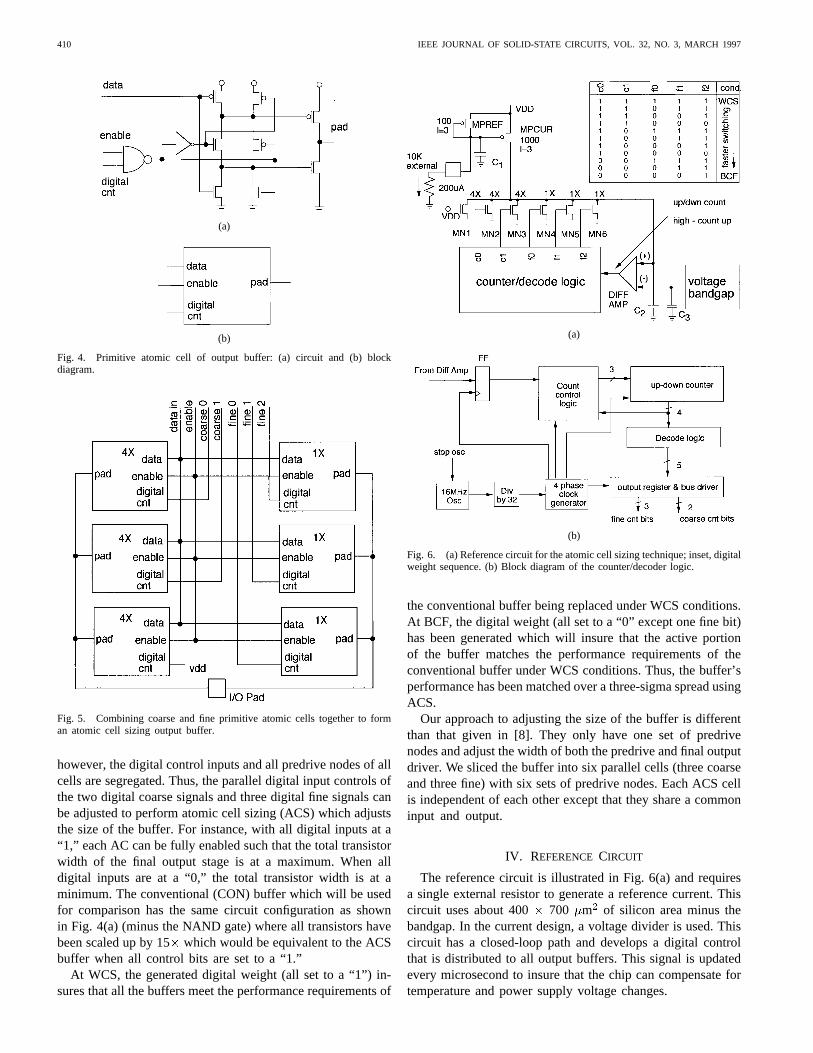
Fig. 4(a) illustrates the primitive atomic cell of an outputbuffer, while Fig. 4(b) gives the block diagram representation.The digital control signal applied to the NAND gate is usedto enable/disable that particular primitive cell. This cell alsocontains two additional input signals; enable—used to tristatethe buffer, and data—the input signal which will be transferredto the pad.
A buffer consists of several of these primitive cells placedin parallel. As shown in Fig. 5, an atomic cell (AC) consistsof three fine (1 ) and three coarse (4) primitive AC’s placedin parallel. One coarse cell is equivalent to four fine cells. Alloutput buffers are formed using this combination of primitivecells. Note that the lower left coarse cell has a solid inputof VDD applied to the digital control. This insures that theminimum size of this buffer cannot decrease below that of acoarse cell. All the enable, data, and pad leads are common;
410 IEEE JOURNAL OF SOLID-STATE CIRCUITS, VOL. 32, NO. 3, MARCH 1997
(a)
(b)
Fig. 4. Primitive atomic cell of output buffer: (a) circuit and (b) blockdiagram.
Fig. 5. Combining coarse and fine primitive atomic cells together to forman atomic cell sizing output buffer.
however, the digital control inputs and all predrive nodes of allcells are segregated. Thus, the parallel digital input controls ofthe two digital coarse signals and three digital fine signals canbe adjusted to perform atomic cell sizing (ACS) which adjuststhe size of the buffer. For instance, with all digital inputs at a“1,” each AC can be fully enabled such that the total transistorwidth of the final output stage is at a maximum. When alldigital inputs are at a “0,” the total transistor width is at aminimum. The conventional (CON) buffer which will be usedfor comparison has the same circuit configuration as shownin Fig. 4(a) (minus the NAND gate) where all transistors havebeen scaled up by 15which would be equivalent to the ACSbuffer when all control bits are set to a “1.”
At WCS, the generated digital weight (all set to a “1”) in-sures that all the buffers meet the performance requirements of
(a)
(b)
Fig. 6. (a) Reference circuit for the atomic cell sizing technique; inset, digitalweight sequence. (b) Block diagram of the counter/decoder logic.
the conventional buffer being replaced under WCS conditions.At BCF, the digital weight (all set to a “0” except one fine bit)has been generated which will insure that the active portionof the buffer matches the performance requirements of theconventional buffer under WCS conditions. Thus, the buffer’sperformance has been matched over a three-sigma spread usingACS.
Our approach to adjusting the size of the buffer is differentthan that given in [8]. They only have one set of predrivenodes and adjust the width of both the predrive and final outputdriver. We sliced the buffer into six parallel cells (three coarseand three fine) with six sets of predrive nodes. Each ACS cellis independent of each other except that they share a commoninput and output.
IV. REFERENCE CIRCUIT
The reference circuit is illustrated in Fig. 6(a) and requiresa single external resistor to generate a reference current. Thiscircuit uses about 400 700 m of silicon area minus thebandgap. In the current design, a voltage divider is used. Thiscircuit has a closed-loop path and develops a digital controlthat is distributed to all output buffers. This signal is updatedevery microsecond to insure that the chip can compensate fortemperature and power supply voltage changes.
GABARA et al.: FORMING DAMPED LRC PARASITIC CIRCUITS 411
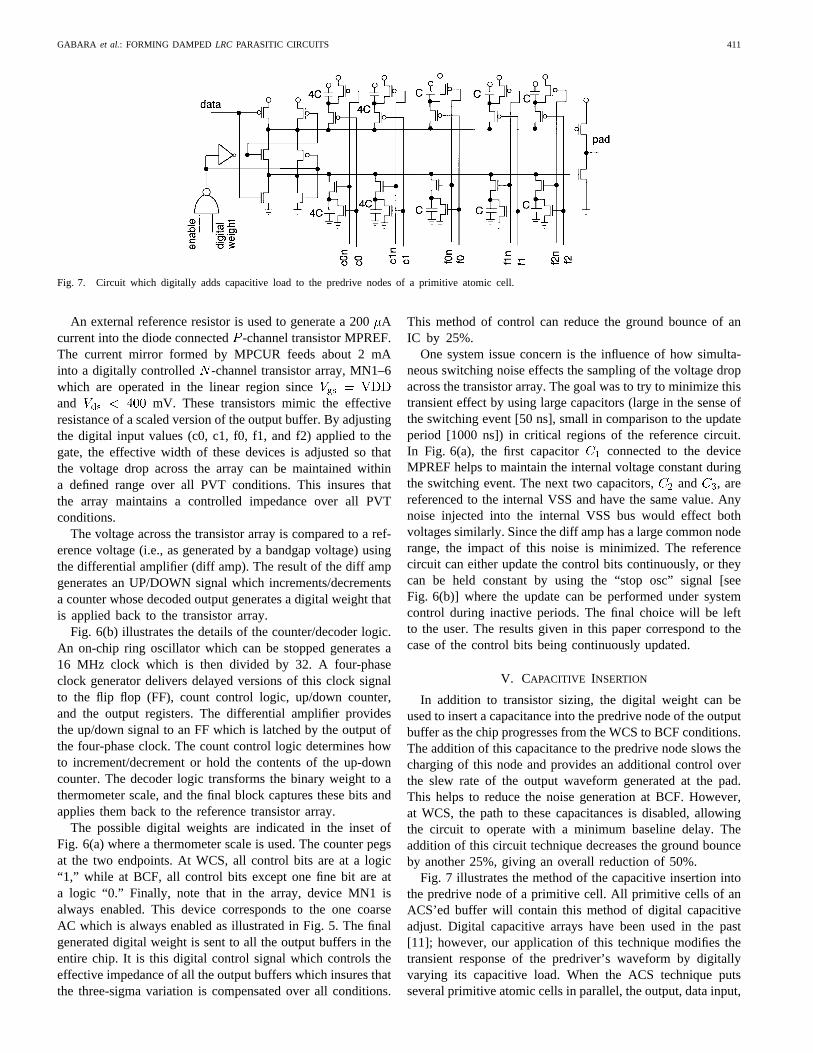
Fig. 7. Circuit which digitally adds capacitive load to the predrive nodes of a primitive atomic cell.
An external reference resistor is used to generate a 200Acurrent into the diode connected-channel transistor MPREF.The current mirror formed by MPCUR feeds about 2 mAinto a digitally controlled -channel transistor array, MN1–6which are operated in the linear region sinceand mV. These transistors mimic the effectiveresistance of a scaled version of the output buffer. By adjustingthe digital input values (c0, c1, f0, f1, and f2) applied to thegate, the effective width of these devices is adjusted so thatthe voltage drop across the array can be maintained withina defined range over all PVT conditions. This insures thatthe array maintains a controlled impedance over all PVTconditions.
The voltage across the transistor array is compared to a ref-erence voltage (i.e., as generated by a bandgap voltage) usingthe differential amplifier (diff amp). The result of the diff ampgenerates an UP/DOWN signal which increments/decrementsa counter whose decoded output generates a digital weight thatis applied back to the transistor array.
Fig. 6(b) illustrates the details of the counter/decoder logic.An on-chip ring oscillator which can be stopped generates a16 MHz clock which is then divided by 32. A four-phaseclock generator delivers delayed versions of this clock signalto the flip flop (FF), count control logic, up/down counter,and the output registers. The differential amplifier providesthe up/down signal to an FF which is latched by the output ofthe four-phase clock. The count control logic determines howto increment/decrement or hold the contents of the up-downcounter. The decoder logic transforms the binary weight to athermometer scale, and the final block captures these bits andapplies them back to the reference transistor array.
The possible digital weights are indicated in the inset ofFig. 6(a) where a thermometer scale is used. The counter pegsat the two endpoints. At WCS, all control bits are at a logic“1,” while at BCF, all control bits except one fine bit are ata logic “0.” Finally, note that in the array, device MN1 isalways enabled. This device corresponds to the one coarseAC which is always enabled as illustrated in Fig. 5. The finalgenerated digital weight is sent to all the output buffers in theentire chip. It is this digital control signal which controls theeffective impedance of all the output buffers which insures thatthe three-sigma variation is compensated over all conditions.
This method of control can reduce the ground bounce of anIC by 25%.
One system issue concern is the influence of how simulta-neous switching noise effects the sampling of the voltage dropacross the transistor array. The goal was to try to minimize thistransient effect by using large capacitors (large in the sense ofthe switching event [50 ns], small in comparison to the updateperiod [1000 ns]) in critical regions of the reference circuit.In Fig. 6(a), the first capacitor connected to the deviceMPREF helps to maintain the internal voltage constant duringthe switching event. The next two capacitors, and , arereferenced to the internal VSS and have the same value. Anynoise injected into the internal VSS bus would effect bothvoltages similarly. Since the diff amp has a large common noderange, the impact of this noise is minimized. The referencecircuit can either update the control bits continuously, or theycan be held constant by using the “stop osc” signal [seeFig. 6(b)] where the update can be performed under systemcontrol during inactive periods. The final choice will be leftto the user. The results given in this paper correspond to thecase of the control bits being continuously updated.
V. CAPACITIVE INSERTION
In addition to transistor sizing, the digital weight can beused to insert a capacitance into the predrive node of the outputbuffer as the chip progresses from the WCS to BCF conditions.The addition of this capacitance to the predrive node slows thecharging of this node and provides an additional control overthe slew rate of the output waveform generated at the pad.This helps to reduce the noise generation at BCF. However,at WCS, the path to these capacitances is disabled, allowingthe circuit to operate with a minimum baseline delay. Theaddition of this circuit technique decreases the ground bounceby another 25%, giving an overall reduction of 50%.
Fig. 7 illustrates the method of the capacitive insertion intothe predrive node of a primitive cell. All primitive cells of anACS’ed buffer will contain this method of digital capacitiveadjust. Digital capacitive arrays have been used in the past[11]; however, our application of this technique modifies thetransient response of the predriver’s waveform by digitallyvarying its capacitive load. When the ACS technique putsseveral primitive atomic cells in parallel, the output, data input,
412 IEEE JOURNAL OF SOLID-STATE CIRCUITS, VOL. 32, NO. 3, MARCH 1997
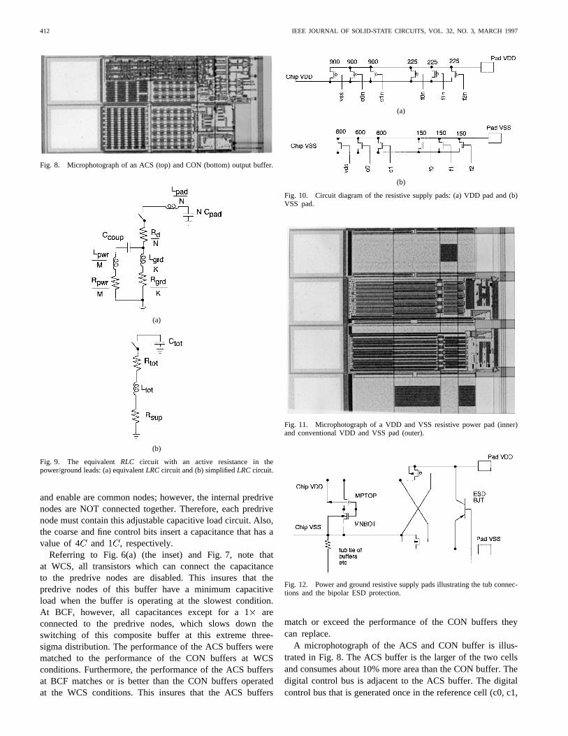
Fig. 8. Microphotograph of an ACS (top) and CON (bottom) output buffer.
(a)
(b)
Fig. 9. The equivalentRLC circuit with an active resistance in thepower/ground leads: (a) equivalentLRCcircuit and (b) simplifiedLRCcircuit.
and enable are common nodes; however, the internal predrivenodes are NOT connected together. Therefore, each predrivenode must contain this adjustable capacitive load circuit. Also,the coarse and fine control bits insert a capacitance that has avalue of 4 and 1 , respectively.
Referring to Fig. 6(a) (the inset) and Fig. 7, note thatat WCS, all transistors which can connect the capacitanceto the predrive nodes are disabled. This insures that thepredrive nodes of this buffer have a minimum capacitiveload when the buffer is operating at the slowest condition.At BCF, however, all capacitances except for a 1areconnected to the predrive nodes, which slows down theswitching of this composite buffer at this extreme three-sigma distribution. The performance of the ACS buffers werematched to the performance of the CON buffers at WCSconditions. Furthermore, the performance of the ACS buffersat BCF matches or is better than the CON buffers operatedat the WCS conditions. This insures that the ACS buffers
(a)
(b)
Fig. 10. Circuit diagram of the resistive supply pads: (a) VDD pad and (b)VSS pad.
Fig. 11. Microphotograph of a VDD and VSS resistive power pad (inner)and conventional VDD and VSS pad (outer).
Fig. 12. Power and ground resistive supply pads illustrating the tub connec-tions and the bipolar ESD protection.
match or exceed the performance of the CON buffers theycan replace.
A microphotograph of the ACS and CON buffer is illus-trated in Fig. 8. The ACS buffer is the larger of the two cellsand consumes about 10% more area than the CON buffer. Thedigital control bus is adjacent to the ACS buffer. The digitalcontrol bus that is generated once in the reference cell (c0, c1,
GABARA et al.: FORMING DAMPED LRC PARASITIC CIRCUITS 413
(a)
(b)
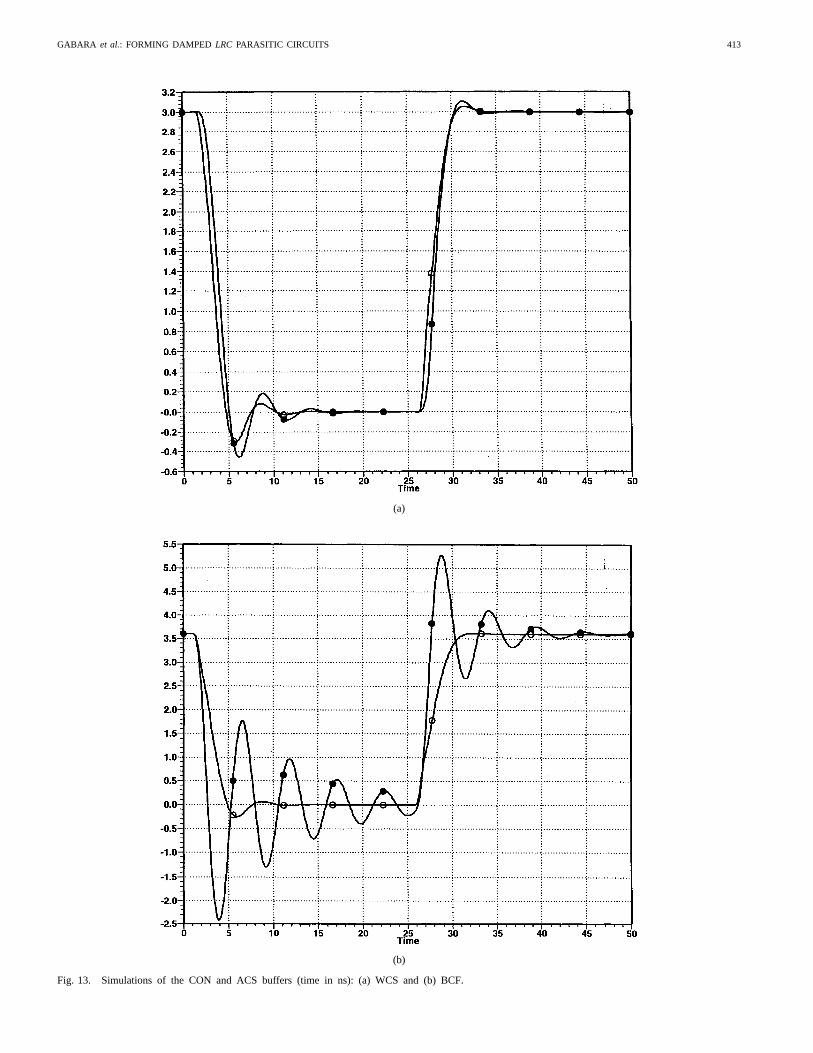
Fig. 13. Simulations of the CON and ACS buffers (time in ns): (a) WCS and (b) BCF.
414 IEEE JOURNAL OF SOLID-STATE CIRCUITS, VOL. 32, NO. 3, MARCH 1997
f0, f1, and f2) runs adjacent to the ACS buffer and is appliedto all ACS output buffers. Furthermore, the primitive atomiccell of the output buffer can be scaled to create buffers withdifferent current sinking capabilities. Thus, only one referencecell is required per chip which can be shared by all outputbuffers.
VI. DAMPED LRC CIRCUIT
In some cases, a quieter buffer may be desirable. If thedesigner attempted to design this buffer, then the effective re-sistance would need to be increased but the performance wouldbe compromised. In this scenario, the buffer will generate lessground bounce. By adding another circuit element into thecircuit of Fig. 2, the designer can achieve a faster buffer yetstill potentially allow (5b) to be approached. If a resistance isplaced in series with the inductance which is in the VDD andVSS leads of Fig. 1, this resistance can be used to dampenthe oscillations. The equivalentLRC circuit is illustrated inFig. 9(a). The two additional resistors and arescaled according to the number of occurrences (or ) ofVDD or VSS pads, respectively. Since the number of outputs
is typically greater than either or , this additionalresistance is not scaled as rapidly as the resistance of the outputbuffer. Thus, the performance of a single buffer is barelydegraded, while the damping effect when all output buffersswitch can be significantly reduced. Note that the resistanceof will depend on the number of outputs that are drivenfrom a “1” to a “0.” Those outputs which remain constant willact as decoupling capacitances and help to reduce the groundbounce. These added resistors, and , are always inthe circuit to help in damping the circuit. The simplifiedLRCcircuit is given in Fig. 9(b).
This additional resistance can be formed from passive com-ponents, but passive resistance (i.e., poly, n, p ) can vary
30%. In order to maintain a more constant resistance, activedevices are used that will be controlled by the same digitalweight that has already been generated by the reference circuit.The active resistive elements are illustrated in Fig. 10(a) and(b). A microphotograph (Fig. 11) shows the resistive VDD andVSS power pads alongside conventional VDD and VSS powerpads. Note that the active transistors forming the resistanceare placed into the I/O cell, thereby saving area. These digitalcontrol busses can be seen adjacent to the cells. At WCS,all the devices will be enabled to minimize the resistanceso a maximum specified voltage drop is satisfied. At BCF,these devices will again be adjusted to insure that the overallimpedance in the overallLRC tanks circuit remains constantor the same value as at WCS. Thus, this technique allows anindependent ground bounce control over and above that of thecontrol incorporated in the output buffer.
Several sets of these VDD and VSS pads may be requiredto match the package requirements to the buffer specifications.This technique will allow a wider range of buffer use in variousdesigns. Fig. 12 depicts the equivalent circuit of the powernetwork in the IC when the resistive VSS and VDD pads areused. Note that the p-channel MPTOP can have a separate n-
Fig. 14. Microphotograph of 0.5-�m CMOS test chip.
tub and can be tied to the pad. However, since psubstrateis used, the tub tie of the MNBOT must be connected tothe internal chip VSS bus. This prevents the substrate fromshorting out the impedance of the device MNBOT.
For those output buffers that may be required to sink aspecified amount of current, the effect of the voltage dropacross the resistance introduced into the power/ground supplyleads needs to be addressed. It is essential that when all buffersare sinking their required current, the summation of the currentflowing through the ground lead does not significantly raise thepotential drop on the internal VSS bus which could cause thevoltage drop measured on the output of the buffers to exceedthe specification. Although the addition of this resistance helpsto dampen theLRCcircuit, care needs to be exercised to insurethat this specification is not violated.
VII. SIMULATION RESULTS
ADVICE (internal Lucent SPICE) simulations were used tocompare the performance and the effects of theRLC networkon the ACS buffers and the CON buffers. The capacitive loadof the output buffer was a 50 pF lumped load, while thetotal series inductance was 14 nH. Fig. 13(a) compares thewaveforms of the ACS buffer (open circle) to the CON buffer(solid circle) under WCS conditions. The worst case delayof the ACS buffer is less than that of the comparable CONbuffer. Fig. 13(b) compares the same output waveforms underthe BCF conditions. The three-sigma spread demonstrates itseffect on the CON buffers; note that the CON waveforms ringdue to the reduction of [see (5a) and (6)]. The ACSbuffers, however, maintain a constant resistance which insuresa clean waveform. Note the similarity of the waveforms of theACS buffer between the WCS and BCF simulations. Since thedelay and ground bounce between these two cases changed
GABARA et al.: FORMING DAMPED LRC PARASITIC CIRCUITS 415
(a)
(b)
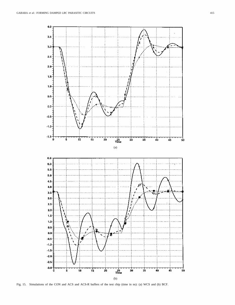
Fig. 15. Simulations of the CON and ACS and ACS-R buffers of the test chip (time in ns): (a) WCS and (b) BCF.
416 IEEE JOURNAL OF SOLID-STATE CIRCUITS, VOL. 32, NO. 3, MARCH 1997
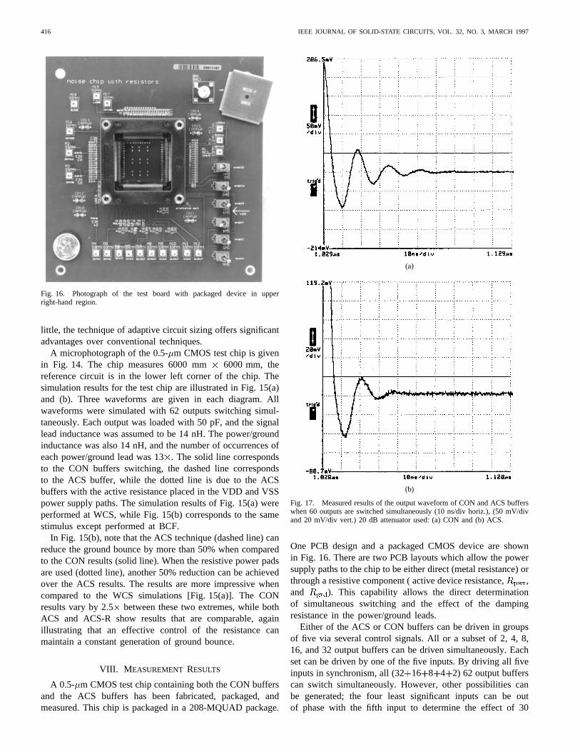
Fig. 16. Photograph of the test board with packaged device in upperright-hand region.
little, the technique of adaptive circuit sizing offers significantadvantages over conventional techniques.
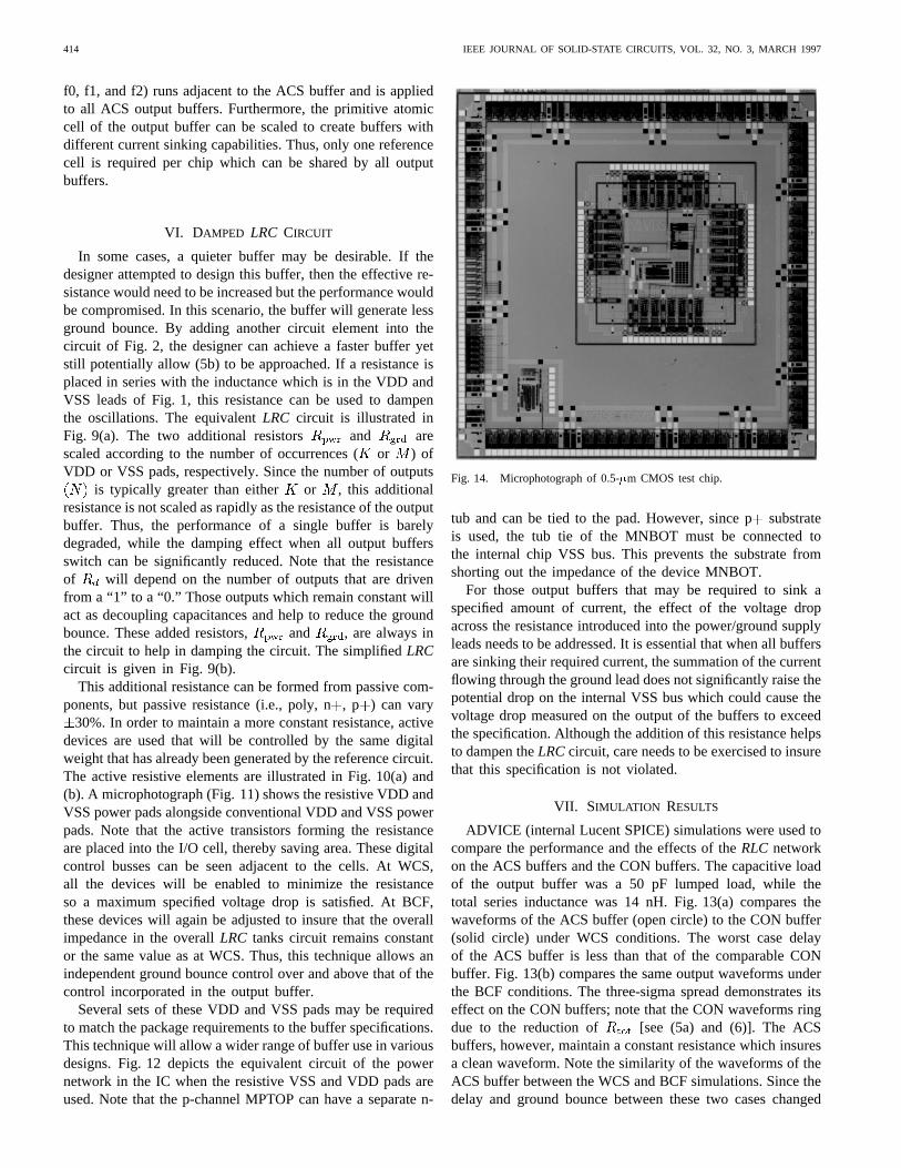
A microphotograph of the 0.5-m CMOS test chip is givenin Fig. 14. The chip measures 6000 mm 6000 mm, thereference circuit is in the lower left corner of the chip. Thesimulation results for the test chip are illustrated in Fig. 15(a)and (b). Three waveforms are given in each diagram. Allwaveforms were simulated with 62 outputs switching simul-taneously. Each output was loaded with 50 pF, and the signallead inductance was assumed to be 14 nH. The power/groundinductance was also 14 nH, and the number of occurrences ofeach power/ground lead was 13. The solid line correspondsto the CON buffers switching, the dashed line correspondsto the ACS buffer, while the dotted line is due to the ACSbuffers with the active resistance placed in the VDD and VSSpower supply paths. The simulation results of Fig. 15(a) wereperformed at WCS, while Fig. 15(b) corresponds to the samestimulus except performed at BCF.
In Fig. 15(b), note that the ACS technique (dashed line) canreduce the ground bounce by more than 50% when comparedto the CON results (solid line). When the resistive power padsare used (dotted line), another 50% reduction can be achievedover the ACS results. The results are more impressive whencompared to the WCS simulations [Fig. 15(a)]. The CONresults vary by 2.5 between these two extremes, while bothACS and ACS-R show results that are comparable, againillustrating that an effective control of the resistance canmaintain a constant generation of ground bounce.
VIII. M EASUREMENT RESULTS
A 0.5- m CMOS test chip containing both the CON buffersand the ACS buffers has been fabricated, packaged, andmeasured. This chip is packaged in a 208-MQUAD package.
(a)
(b)
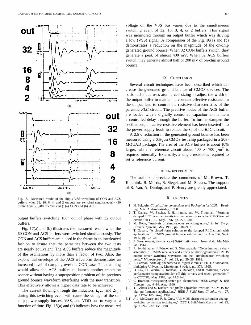
Fig. 17. Measured results of the output waveform of CON and ACS bufferswhen 60 outputs are switched simultaneously (10 ns/div horiz.), (50 mV/divand 20 mV/div vert.) 20 dB attenuator used: (a) CON and (b) ACS.
One PCB design and a packaged CMOS device are shownin Fig. 16. There are two PCB layouts which allow the powersupply paths to the chip to be either direct (metal resistance) orthrough a resistive component ( active device resistance,,and ). This capability allows the direct determinationof simultaneous switching and the effect of the dampingresistance in the power/ground leads.
Either of the ACS or CON buffers can be driven in groupsof five via several control signals. All or a subset of 2, 4, 8,16, and 32 output buffers can be driven simultaneously. Eachset can be driven by one of the five inputs. By driving all fiveinputs in synchronism, all (3216 8 4 2) 62 output bufferscan switch simultaneously. However, other possibilities canbe generated; the four least significant inputs can be outof phase with the fifth input to determine the effect of 30
GABARA et al.: FORMING DAMPED LRC PARASITIC CIRCUITS 417
(a)
(b)
Fig. 18. Measured results of the chip’s VSS waveform of CON and ACSbuffers when 32, 16, 8, 4, and 2 outputs are switched simultaneously (20ns/div horiz.), (200 mV/div vert.): (a) CON and (b) ACS.
output buffers switching 180out of phase with 32 outputbuffers.
Fig. 17(a) and (b) illustrates the measured results when the60 CON and ACS buffers were switched simultaneously. TheCON and ACS buffers are placed in the frame in an interleavedfashion to insure that the parasitics between the two testsare nearly equivalent. The ACS buffers reduce the magnitudeof the oscillations by more than a factor of two. Also, theexponential envelope of the ACS waveform demonstrates anincreased level of damping over the CON case. This dampingwould allow the ACS buffers to launch another transitionsooner without having a superposition problem of the previousground bounce waveform interfering with the new transition.This effectively allows a higher data rate to be achieved.
The current flowing through the inductors andduring this switching event will cause the voltage of the on-chip power supply busses, VSS, and VDD bus to vary as afunction of time. Fig. 18(a) and (b) indicates how the measured
voltage on the VSS bus varies due to the simultaneousswitching event of 32, 16, 8, 4, or 2 buffers. This signalwas monitored through an output buffer which was drivinga low (VSS) signal. A comparison of the Fig. 18(a) and (b)demonstrates a reduction on the magnitude of the on-chipgenerated ground bounce. When 32 CON buffers switch, theygenerate a peak of almost 400 mV. When 32 ACS buffersswitch, they generate almost half or 200 mV of on-chip groundbounce.
IX. CONCLUSION
Several circuit techniques have been described which de-crease the generated ground bounce of CMOS devices. Thebasic technique uses atomic cell sizing to adjust the width ofthe output buffer to maintain a constant effective resistance inthe output lead to control the resistive characteristics of theparasiticRLC circuit. The predrive nodes of the ACS bufferare loaded with a digitally controlled capacitor to maintaina controlled delay through the buffer. To further dampen theoscillations, an active resistive element has been inserted intothe power supply leads to reduce theof the RLC circuit.
A 2.5 reduction in the generated ground bounce has beenmeasured using a 0.5-m CMOS test chip packaged in a 208-MQUAD package. The area of the ACS buffers is about 10%larger, while a reference circuit about 400 700 m isrequired internally. Externally, a single resistor is required toset a reference current.
ACKNOWLEDGMENT
The authors appreciate the comments of M. Brown, T.Karanink, B. Morris, S. Siegel, and M. Strauss. The supportof R. Yan, A. Dunlop, and P. Henry are greatly appreciated.
REFERENCES
[1] H. Bakoglu,Circuits, Interconnections and Packaging for VLSI. Read-ing, MA: Addison-Wesley, 1990.
[2] T. Gabara, W. Fischer, J. Harrington, and W. Troutman, “Formingdamped LRC parasitic circuits in simultaneously switched CMOS outputcircuit,” in CICC, May 1996, pp. 277–280.
[3] M. Dolle, “Analysis of simultaneous switching noise,” inInt. Symp.Circuits, Systems, May 1995, pp. 904–907.
[4] T. Gabara, “A closed form solution to the damped RLC circuit withapplications to CMOS ground bounce estimation,” inASIC’96, Sept.1996, pp. 73–78.
[5] J. Groszkowski,Frequency of Self-Oscillations. New York: MacMil-lan, 1964.
[6] R. Senthinathan, J. Prince, and S. Nimmagadda, “Noise immunity char-acteristics of CMOS receivers and effects of skewing/damping CMOSoutput driver switching waveform on the ‘simultaneous’ switchingnoise,” Microelectron. J., vol. 23, pp. 29–36, 1992.
[7] P. Larsson, “Analog phenomena in digital circuits,” Ph.D. dissertation,Linkoping University, Linkoping, Sweden, no. 376, 1995.
[8] D. Cox, D. Guertin, C. Johnson, B. Rudolph, and R. Williams, “VLSIperformance compensation for off-chip drivers and clock generation,”in CICC’89, May 1989, pp. 14.3.1–4.
[9] C. Branson, “Integrating tester pin electronics,”IEEE Design & TestComput., pp. 4–14, Apr. 1990.
[10] T. Gabara and S. Knauer, “Digitally adjustable resistors in CMOS forhigh-performance applications,”IEEE J. Solid-State Circuits, vol. 27,pp. 1176–1185, Aug. 1992.
[11] J. L. McCreary and P. R. Grey, “All-MOS charge redistribution analog-to-digital conversion techniques,”IEEE J. Solid-State Circuits, vol. 23,pp. 1224–1232, Oct. 1988.
418 IEEE JOURNAL OF SOLID-STATE CIRCUITS, VOL. 32, NO. 3, MARCH 1997
Thaddeus J. Gabara (S’77–M’78) received theB.S.E.E. and M.S.E.E. degrees from New JerseyInstitute of Technology, Newark, NJ.
He is a Distinguished Member of the TechnicalStaff at AT&T Bell Laboratories, Murray Hill, NJ, inthe Microsystem Research Department. His experi-ence has covered VLSI design issues involved withareas of microprocessors and telecommunicationCMOS devices. Topics of interests include high per-formance I/O, adaptable circuits, ground bounce re-duction techniques, silicon-on-silicon modules, and
laser driver/receiver systems.Mr. Gabara is a member of the Technical Program Committee of the IEEE
ASIC Conference, the IEEE Custom Integrated Circuit Conference, and theIEEE Multi Chip Module Conference.
Wilhelm C. Fischer holds a B.S.E.E. degree fromNewark College of Engineering, Newark, NJ.
He is a Member of the Technical Staff in theComputing Systems Technology Research Depart-ment at AT&T Bell Laboratories, Murray Hill, NJ.His experience includes work in the design, layout,and verification of VLSI circuits.
John Harrington received the B.S.E.E. degree fromRensselaer Polytechnic Institute, Troy, NY, in 1980and the M.S.E.E. degree from Stanford University,Stanford, CA, in 1981.
He joined Bell Laboratories in 1980 working onintegrated circuit design until 1986. He became theTechnical Manager of the AT&T-MicroelectronicsSunnyvale Design Center in 1986. In 1990, hebecame Department Head of the OEM ASIC De-sign Department. Other responsibilities since thattime include heading up the ASIC Digital and
Mixed-Signal Macrocell groups, LAN Standard Products, and ASIC DesignMethodology directions. He has recently been appointed General Manager ofthe Data Networking Product Line for Lucent Technologies, Allentown, PA.
William W. Troutman earned engineering degreesfrom Pennsylvania State University, State College,the Massachusetts Institute of Technology, Cam-bridge, and Cambridge University, England.
In 1966, he joined AT&T Bell Laboratories,Whippany, NJ, where he worked on the effects ofelectronic pulses on circuits and systems. In 1975,he moved into integrated circuit design at MurrayHill, NJ. At first, he led a Design Team that wasresponsible for various high-speed TTL functions.Later, he had design responsibility for one of the
very first CMOS 4-b microcontrollers. He then led an effort that completedseveral highly complex, 32-b CMOS peripherals. More recently, he reportsto the Chief Scientist of Lucent’s Microelectronics’ Business Unit, where hehandles a variety of business and technical issues.


