Embed Size (px)
Citation preview

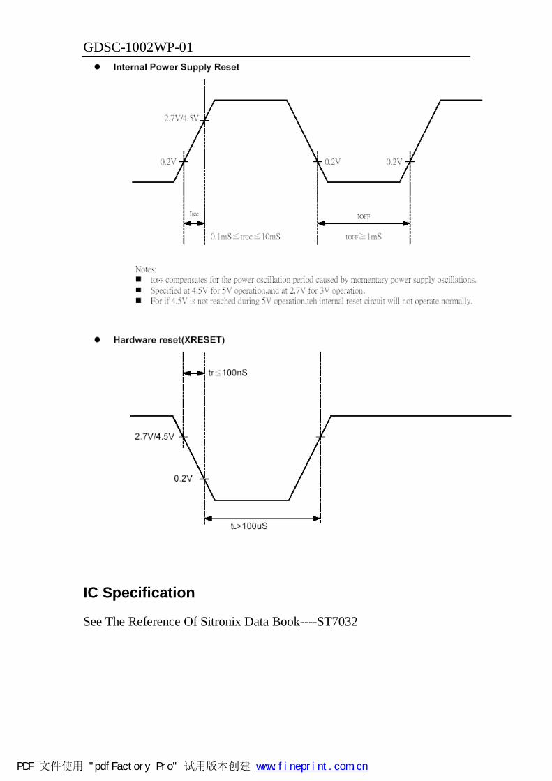
GDSC-1002WP-01
SPECIFICATION
10*2 Dot Matrix LCD Module GDSC1002WP-01
XIAMEN OCULAR LCD DEVIDES CO.,LTD.
PDF 文件使用 "pdfFactory Pro" 试用版本创建 www.fineprint.com.cn

GDSC-1002WP-01
1. General Specification
Interface With Series MPU
Display Specification
Display Mode:FSTN Type
Viewing Angle :6:00 Clock
Display Duty:1/16 Driving Bias:1/5 Driving Voltage:4.5V
Mechanical Characteristics(Unit:mm)
Display Dot Matrix :10*2
Extenal Dimension: See Drawing
Dots Size:0.45*0.55
Dots Pitch:0.50*0.60
Temperature Specification
Operation Temperature:-20~70℃
Storage Temperature:-25~75℃
PDF 文件使用 "pdfFactory Pro" 试用版本创建 www.fineprint.com.cn

GDSC-1002WP-01
External Dimension
1 6
VDD1
6 RS
32
54 DB6(SCL)
CS
VSSDB7(SI)
NO
------------
LCD LAYOUT
COM2COM8
S1
S50
COM16COM10
PIXEL DETAILS
28.1(A,A)
32.1(V,A)
35.1±0.2
11.3
(A,A
)
14.3
(V,A)
17.3±
0.2
25.3±
0.2
13.050.9
PITCH 1.80*5=9.08.6
5MAX
7.0*0.7
0.7*2
MAX 2.0
0.30
(SE
CTIO
N 0
.30
*0.5
0)
4.3±0.5
UV TAPE IC:ST7032
SILICONE
FRO
NT
BA
CK
0.45
0.50
0.5
50.6
0 0.4 3.0
PART NO.
CHECKED BY
DESIGN BY
WGDSC- -1002WP-01
RF
YGBFT
MAX 6.0
0.5 0.3
OPEN0 V4OPF2
CAP1PTEST1
VOUT
TEST4PSB
TEST3
TEST2
SHLC
VINSHLS
OPR2OPR1
OPEN
OPEN
1
OPEN01
OPEN
1
TEST5
0
11
00
OSC1
E
OPF1DB0-DB5
RWOSC2
PINXRESET
TYPE
OPENOPENOPENOPENOPEN
CLSOPENCAP1N
1
01
OPEN1
V1
V3V2
V0
TYPE1 EXT
PIN
10
PDF 文件使用 "pdfFactory Pro" 试用版本创建 www.fineprint.com.cn

GDSC-1002WP-01
PIN Assignment Pin Symbol Function
1 VDD Power supply for logic for LCM
2 VSS Signal ground for LCM (GND)
3 DB7
4 DB6
DB7 can be used as a busy flag.In serial interface
mode DB7 is SI(input data),DB6 is SCL(serial
clock).
5 CS Chip select in parallel mode and serial
interface(Low active)
6 RS Select register.
0:Instruction register (for write) Busy flag
&address counter(for read)
1:Data register(for write and read).
Absolute Maximun Ratings Power supply voltage VDD-VSS 0 - 7.0
Input voltage VIN VSS - VDD
V
Operating temperature range TA -20 - +70
Storage temperature range TSTO -25 - +75 ℃
*Wide temperature range is available
PDF 文件使用 "pdfFactory Pro" 试用版本创建 www.fineprint.com.cn

GDSC-1002WP-01
DC Characteristics Parameter Symbol Conditions Min. Typ. Max. Unit
Supply voltage
for LCD
VDD-V0 Ta =25℃ - 3.3 -
Operating
voltage
VDD 2.7 5.0 5.5
V
Supply current IDD Ta=25 ℃ ,
VDD=5.0V - 0.8 1.0 mA
Input leakage
current
ILKG - - 2.0 uA
“H” level
input voltage
VIH 2.2 - VDD
“L” level
input voltage
VIL Twice initial
value or less 0 - 0.6
“H” level
output voltage
VOH LOH=-0.25mA 2.4 - -
“L” level
output voltage
VOL LOH=1.6mA - - 0.4
Backlight
supply voltage
VF - 5.0 -
V
PDF 文件使用 "pdfFactory Pro" 试用版本创建 www.fineprint.com.cn

GDSC-1002WP-01
AC Characteristics
PDF 文件使用 "pdfFactory Pro" 试用版本创建 www.fineprint.com.cn
GDSC-1002WP-01
IC Specification
See The Reference Of Sitronix Data Book----ST7032
PDF 文件使用 "pdfFactory Pro" 试用版本创建 www.fineprint.com.cn

GDSC-1002WP-01
Display Data RAM(DDRAM)
PDF 文件使用 "pdfFactory Pro" 试用版本创建 www.fineprint.com.cn

GDSC-1002WP-01
Instruction Table
PDF 文件使用 "pdfFactory Pro" 试用版本创建 www.fineprint.com.cn

GDSC-1002WP-01
Instruction Description To overcome the speed difference between the internal clock of ST7032 and
the MPU clock, ST7032 performs internal operations by storing control in
formations to IR or DR. The internal operation is determined according
to the signal from MPU, composed of read/write and data bus .
Instructions can be divided largely into four groups:
1) ST7032 function set instructions (set display methods, set data
length, etc.)
2) Address set instructions to internal RAM
3) Data transfer instructions with internal RAM
The address of the internal RAM is automatically increased or decreased
by 1.
Note: during internal operation, busy flag (DB7) is read “High”.
Busy flag check must be preceded by the next instruction.
When an MPU program with checking the busy flag (DB7) is made, it
must be necessary 1/2 fuss for executing the next instruction by the
falling edge of the “E” signal after the busy flag (DB7) goes to
“LOW”.
Contents
1) Clear Display
RS R/W DB7 DB6 DB5 DB4 DB3 DB2 DB1 DB0
0 0 0 0 0 0 0 0 0 1
Clear all the display data by writing “20H” (space code) to all DDRAM
address, and set DDRAM address to “00H” into AC (address counter).
Return cursor to the original status, namely, brings the cursor to the
left edge on the fist line of the display.
Make the entry mode increment (I/D=“High”).
2) Return Home
RS R/W DB7 DB6 DB5 DB4 DB3 DB2 DB1 DB0
0 0 0 0 0 0 0 0 1 ×
Return home is cursor return home instruction.
Set DDRAM address to “00H” into the address counter.
Return cursor to its original site and return display to its original
status, if shifted.
Contents of DDRAM does not change.
3) Entry Mode Set
RS R/W DB7 DB6 DB5 DB4 DB3 DB2 DB1 DB0
0 0 0 0 0 0 0 1 I/D S
Set the moving direction of cursor and display.
I/D: increment / decrement of DDRAM address (cursor or blink)
When I/D=“high”, cursor/blink moves to right and DDRAM address is
increased by 1.
PDF 文件使用 "pdfFactory Pro" 试用版本创建 www.fineprint.com.cn

GDSC-1002WP-01 When I/D=“Low”, cursor/blink moves to left and DDRAM address is
increased by 1.
*CGRAM operates the same way as DDRAM, when reading from or writing to
CGRAM.
S: Shift Of Entire Display
When DDRAM read (CGRAM read/write) operation or S=“Low”, shift of entire
display is not performed..
If S=“High” and DDRAM write operation, shift of entire display is
performed according to I/D value.
(I/D=“High”. Shift left, I/D=“Low”. Shift right).
S I/D Description
H H Shift display to the left
H L Shift display to the right
4) Display ON/OFF
RS R/W DB7 DB6 DB5 DB4 DB3 DB2 DB1 DB0
0 0 0 0 0 0 1 D C B
Control display/cursor/blink ON/OFF 1 bit register.
D: Display ON/OFF Control Bit
When D=“High”, entire display is turned on.
When D=“Low”, display is turned off, but display data remains in DDRAM.
C: Cursor ON/OFF Control Bit
When D=“High”, cursor is turned on.
When D=“Low”, cursor is disappeared in current display, but I/D register
preserves its data.
B: Cursor Blink ON/OFF Control Bit
When B=“High”, cursor blink is on, which performs alternately between
all the “High” data and display characters at the cursor position.
When B=“Low”, blink is off.
5) Cursor Or Display Shift
RS R/W DB7 DB6 DB5 DB4 DB3 DB2 DB1 DB0
0 0 0 0 0 1 S/C R/L × ×
S/C:Screen/Cursor Select Bit.
When S/C=”High”,Screen is controlled by R/L bit.
When S/C=”low”,Cursor is controlled by R/L bit.
R/L:Right/Left
When R/L=”High”,set direction to right.
When R/L=”Low”,set direction to left.
Without writing or reading of display data, Shifting of right/left cursor
position or display. This instruction is used to correct or search display
PDF 文件使用 "pdfFactory Pro" 试用版本创建 www.fineprint.com.cn
GDSC-1002WP-01 data. During 2-line mode display, cursor moves to the 2nd line after the
40th digit of the 1st line.Note that display shift is performed
simultaneously in all the line.
When display data is shifted repeatedly, each line is shifted
individually.
When display shift is performed, the contents of the address counter are
not changed.
Shift Patterns According To S/C And R/L Bits
S/C R/L Description AC Value
L L Shift cursor to the left, AC=AC-1
L H Shift cursor to the right AC=AC+1
H L Shift all the display to the left, cursor
moves according to the display
AC=AC
H H Shift all the display to the right, cursor
moves according to the display
AC=AC
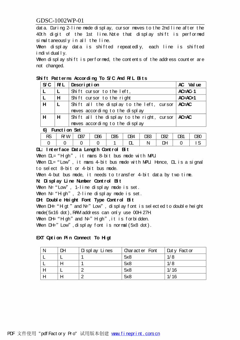
6) Function Set
RS R/W DB7 DB6 DB5 DB4 DB3 DB2 DB1 DB0
0 0 0 0 1 DL N DH 0 IS
DL: Interface Data Length Control Bit
When DL=“High”, it mans 8-bit bus mode with MPU.
When DL=“Low”, it mans 4-bit bus mode with MPU. Hence, DL is a signal
to select 8-bit or 4-bit bus mode.
When 4-but bus mode, it needs to transfer 4-bit data by two time.
N: Display Line Number Control Bit
When N=“Low”, 1-line display mode is set.
When N=“High”, 2-line display mode is set.
DH: Double Height Font Type Control Bit
When DH=“Higt”and N=”Low”, display font is selected to double height
mode(5x16 dot),RAM address can only use 00H-27H.
When DH=“High”and N=”High”,it is forbidden.
When DH=”Low”,display font is normal(5x8 dot).
EXT Option Pin Connect To Higt
N DH Display Lines Character Font Duty Factor
L L 1 5x8 1/8
L H 1 5x8 1/8
H L 2 5x8 1/16
H H 2 5x8 1/16
PDF 文件使用 "pdfFactory Pro" 试用版本创建 www.fineprint.com.cn
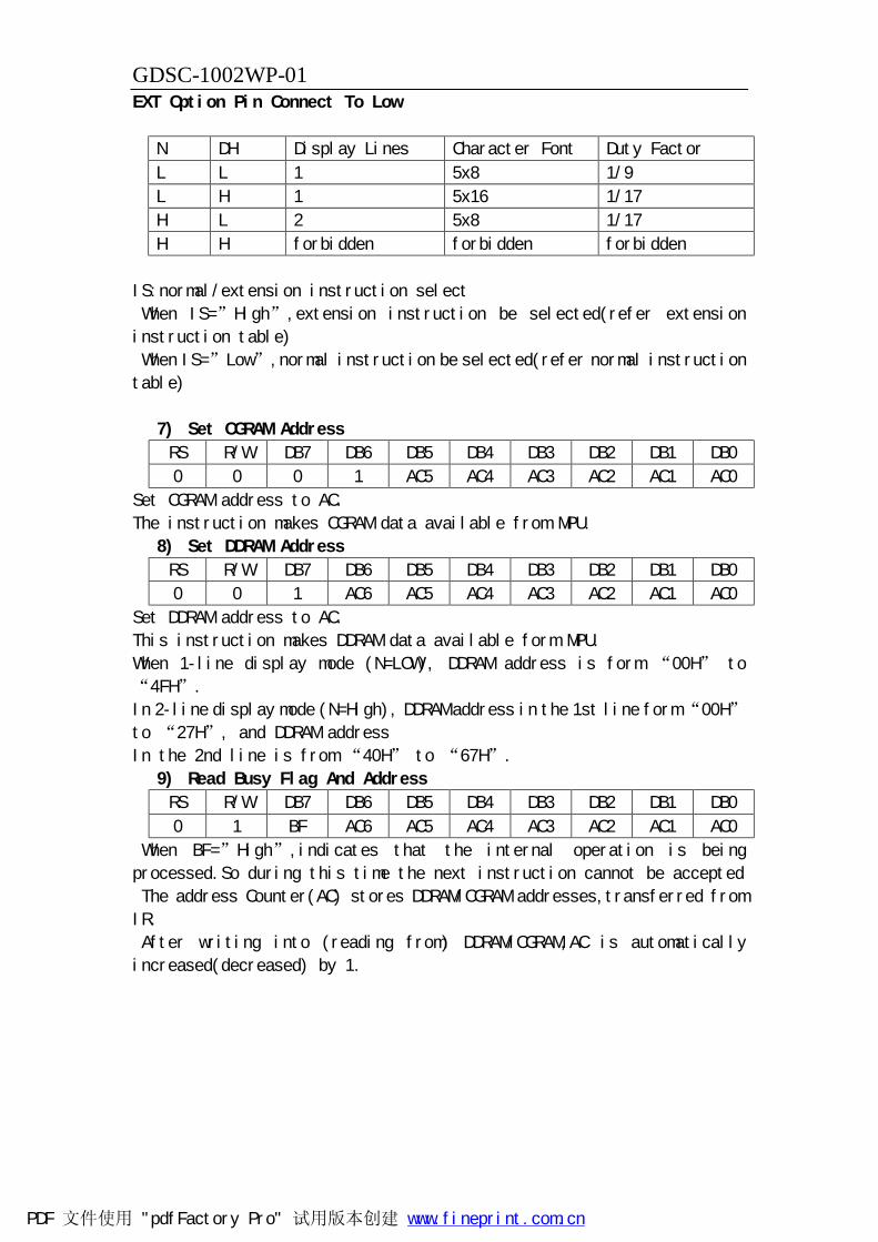
GDSC-1002WP-01 EXT Option Pin Connect To Low
N DH Display Lines Character Font Duty Factor
L L 1 5x8 1/9
L H 1 5x16 1/17
H L 2 5x8 1/17
H H forbidden forbidden forbidden
IS:normal/extension instruction select
When IS=”High”,extension instruction be selected(refer extension
instruction table)
When IS=”Low”,normal instruction be selected(refer normal instruction
table)
7) Set CGRAM Address
RS R/W DB7 DB6 DB5 DB4 DB3 DB2 DB1 DB0
0 0 0 1 AC5 AC4 AC3 AC2 AC1 AC0
Set CGRAM address to AC.
The instruction makes CGRAM data available from MPU.
8) Set DDRAM Address
RS R/W DB7 DB6 DB5 DB4 DB3 DB2 DB1 DB0
0 0 1 AC6 AC5 AC4 AC3 AC2 AC1 AC0
Set DDRAM address to AC.
This instruction makes DDRAM data available form MPU.
When 1-line display mode (N=LOW), DDRAM address is form “00H” to
“4FH”.
In 2-line display mode (N=High), DDRAM address in the 1st line form “00H”
to “27H”, and DDRAM address
In the 2nd line is from “40H” to “67H”.
9) Read Busy Flag And Address
RS R/W DB7 DB6 DB5 DB4 DB3 DB2 DB1 DB0
0 1 BF AC6 AC5 AC4 AC3 AC2 AC1 AC0
When BF=”High”,indicates that the internal operation is being
processed.So during this time the next instruction cannot be accepted
The address Counter(AC) stores DDRAM/CGRAM addresses,transferred from
IR.
After writing into (reading from) DDRAM/CGRAM,AC is automatically
increased(decreased) by 1.
PDF 文件使用 "pdfFactory Pro" 试用版本创建 www.fineprint.com.cn

GDSC-1002WP-01 10) Write Data To CGRAM,DDRAM or ICON RAM
RS R/W DB7 DB6 DB5 DB4 DB3 DB2 DB1 DB0
1 0 D7 D6 D5 D4 D3 D2 D1 D0
Write binary 8-bit data to DDRAM,CGRAM or ICON RAM
The selection of RAM from DDRAM, CGRAM or ICON RAM, is set by the previous
address set instruction (DDRAM address set, CGRAM address set,ICON RAM
address set).
RAM set instruction can also determine the AC direction to RAM.
After write operation.,The address is automatically increased/decreased
by 1, according to the entry mode.
11) Read Data From CGRAM,DDRAM or ICON RAM
RS R/W DB7 DB6 DB5 DB4 DB3 DB2 DB1 DB0
1 1 D7 D6 D5 D4 D3 D2 D1 D0
Read binary 8-bit data from DDRAM/CGRAM/ICON RAM
The selection of RAM is set by the previous address set instruction. If
the address set instruction of RAM is not performed before this
instruction, the data that read first is invalid, because the direction
of AC is not determined. If you read RAM data several times without RAM
address set instructions before read operation, the correct RAM data can
be obtained from the second. But the first data would be incorrect, because
there is no time margin to transfer RAM data.
PDF 文件使用 "pdfFactory Pro" 试用版本创建 www.fineprint.com.cn

GDSC-1002WP-01 12) Bias Selection/Internal OSC Frequency Adjust
RS
R/W
DB7
DB6
DB5 DB4 DB3 DB2 DB1 DB0
0 0 0 0 0 1 BS F2 F1 F0
BS:bias selection
When BS=”High”,the bias will be 1/4
When BS=”Low”,the bias will be 1/5
BS will be invalid when external bias resistors are
used(OPF1=1,OPF2=1)
F2,F1,F0:Internal OSC frequency adjust
When CLS connect to high,that instruction can adjust OSC and Frame
frequency.
F2 F1 F0 Frame 1/9 duty Frame 1/17 duty
0 0 0 105.0 112.0
0 0 1 113.6 120.5
0 1 0 123.5 129.9
0 1 1 137.0 144.9
1 0 0 153.8 163.9
1 0 1 181.8 192.3
1 1 0 227.3 238.1
1 1 1 294.1 312.5
13) Set ICON RAM Address
RS R/W DB7 DB6 DB5 DB4 DB3 DB2 DB1 DB0
0 0 0 1 0 0 AC3 AC2 AC1 AC0
Set ICON RAM address to AC]
This instruction makes ICON data available from MPU.
When IS=1 at Extension mode
The ICON RAM address is from “00H” to “0FH”.
14) Power/ICON Control/Contrast Set(High Byte)
RS R/W DB7 DB6 DB5 DB4 DB3 DB2 DB1 DB0
0 0 0 1 0 1 ION BON C5 C4
ION:Set ICON Display On/Off
When ION=”High”,ICON display on.
When ION=”Low”,ICON display off.
BON:Switch Booster Circuit
When BON=”High”,booster circuit is turn on.
When BON=”Low”,booster circuit is turn off.
C5,C4:Contrast set(high byte)
PDF 文件使用 "pdfFactory Pro" 试用版本创建 www.fineprint.com.cn

GDSC-1002WP-01 C5,C4,C3,C2,C1,C0 can only be set when internal follower is used.They
can more precisely adjust the input reference noltage of V0 generator.The
details please refer to the supply voltage for LCD driver.
15) Follower Control
RS R/W DB7 DB6 DB5 DB4 DB3 DB2 DB1 DB0
0 0 0 1 1 0 FON Rab2 Rab1 Rab0
FON:switch follower circuit
FON can only be set when internal follower is used
When FON=”High”,internal follower circuit is turn on.
When FON=”Low”,internal follower circuit is turn off.
Rab2,Rab1,RAB0 :V0 generator amplified ratio
Rab2,Rab1,RAB0 can only be set when internal follower is used.
They can adjust the amplified ratio of V0 generator.The details please
refer to the supply voltage for LCD driver.
16) Contrast Set(Low Byte)
RS R/W DB7 DB6 DB5 DB4 DB3 DB2 DB1 DB0
0 0 0 1 1 1 C3 C2 C1 C0
C3,C2,C1,C0 can only be set when internal follower is used.
They can more precisely adjust the input reference voltage of V0
generator.The details please refer to the supply voltage for LCD
driver.
PDF 文件使用 "pdfFactory Pro" 试用版本创建 www.fineprint.com.cn

GDSC-1002WP-01
Block Diagram
COM
SEG
RS
DB7
VSSVDD
LCD PANEL
CONTROLLERAND DRIVER
LCD
DB6CS
PDF 文件使用 "pdfFactory Pro" 试用版本创建 www.fineprint.com.cn

GDSC-1002WP-01
Company Profile
XIAMEN OCULAR LCD DEVIDES CO.,LTD. Was formed in 1992. Our company is a joint-venture specializing in manufacturing all kinds of Liquid Crystal Displays. We design and massproduce Touch Panel,LED,COG, the digital segment, dot matrix LCD panels, and modules in TN,HTN and STN types using the advanced and whole facilities and soft-ware technology.
Most of our products are customer_mode. Xiamen Ocular’s LCDs now have a good sale not only in domextic China,but also in America,Europe and East_south Aisa.These LCDs were widely used in the display of instruments,clocks,telecommunication equipments,calcuators,air conditioner controllers and AV systems.
Based upon the reliable high quality, reasonable price and quick delivery, Xiamen Ocular will sever all customers wholeheartedly. Add:South 5/F,Guang Xia Buliding,Tourch Hi-Tech Development Area,Xiamen,China Tel:+86-592-6026045 5652539 5715579 (Sales) +86-592-6026023(R&D) Fax:+86-592-6026021 PC:361006 Web:http://www.lcdchina.com E-mail: [email protected] [email protected] [email protected] (R&D)
PDF 文件使用 "pdfFactory Pro" 试用版本创建 www.fineprint.com.cn


