Embed Size (px)
Citation preview

Growth of functional oxide heterostructuresfrom chemical solutions using advanced
processing methodologies
Dissertation presented in candidacy for the degree of
DOCTORATE OF PHILOSOPHY IN MATERIALS SCIENCE
by
Albert Queraltó López
Supervisors: PROF. TERESA PUIG MOLINA AND DR. ÁNGEL PÉREZ DEL PINO
Tutor: DR. XAVIER GRANADOS GARCIA
Departament de Física, Facultat de Ciències
Doctorat en Ciència de Materials
Universitat Autònoma de Barcelona
Departament de Materials Superconductors i Nanoestructuració a Gran Escala
Institut de Ciència de Materials de Barcelona (ICMAB-CSIC)
Desembre 2014


La Dra. Teresa Puig Molina, Professora d’investigació del CSIC; el Dr. Ángel Pérez del
Pino, Investigador del CSIC i el Dr. Xavier Granados Garcia, Investigador del CSIC tots a
l’Institut de Ciència de Materials de Barcelona
CERTIFIQUEN
que n’Albert Queraltó López, graduat en Física, ha dut a terme sota la seva direcció el
treball que porta per títol “Growth of functional oxide heterostructures from chemical solutions using
advanced processing methodologies” i que queda recollit en aquesta memòria per optar al grau de
Doctor en Ciència de Materials.
I perquè així consti, signem el present certificat.
Prof. Teresa Puig Molina Dr. Ángel Pérez del Pino Dr. Xavier Granados Garcia
Grad. Albert Queraltó López
Bellaterra, Desembre 2014


Acknowledgments
I would like to thank the people and institutions that have made this thesis possible.
First of all, I would like express my gratitude to my supervisors Prof. Teresa Puig Molina
and Dr. Ángel Pérez del Pino for their trust, their helpful advises and the opportunities given
to me. Also, I would like make this acknowledgment extensive to Prof. Xavier Obradors
Berenguer for the helpful discussions and knowledge shared.
This work would have not been possible without the collaboration and interaction with a
good number of scientific experts in various fields:
To all the Superconducting Materials and Nanostructuration Department from the
Materials Science Institute of Barcelona (ICMAB-CSIC). In particular, staff members, previous
PhD students and post-docs with whom I had the opportunity to interact and gave me the
adequate background and complementary knowledge for the research developed in this
thesis, from the solution synthesis to the growth of CSD oxide heterostructures,
characterization and analysis of functional properties.
The TEM experts in our group, M. de la Mata, F. Belarre and Prof. J. Arbiol are deeply
acknowledged. Particularly, M. de la Mata and F. Belarre for their dedication in the preparation
and characterization of TEM samples, and related discussions.
Thanks to R. Vlad for teaching me the experimental tricks when using Chemical Solution
Deposition during my beginnings. Also to X. Palmer, V. Rodríguez and M. de Palau for keeping
us safe in the lab.
Special thanks to Dr. M. Tristany for her help preparing and characterizing BST solutions
and thin-films, and to Dr. M. Gibert for sharing her desk at the beginning and for the overseas
discussions and help during my thesis.
To Dr. S. Ricart, for their willingness to answer my chemical doubts.
To Dr. A. Palau for teaching me how to prepare samples using the four contact method.
I am also very grateful to Prof. S. Trolier-McKinstry from the Materials Research Institute
v

Acknowledgments
at the Pennsylvania State University for having me in her group during a short three-month
stay, and for giving me full access to their equipment. I would like to thank them for the warm
welcome they gave me, and also to her PhD students for the excursions we made. Special
thanks go to Adarsh Rajashekar for his teachings and help using their laser system, also to
Lauren Garten for the interesting discussions about BST films and related properties.
To N. Dix from ICMAB-CSIC for the RHEED characterization of my samples and to Dr. R.
Hühne from the IFW Dresden for the corresponding RHEED analyses.
Dr. J. Santiso from the Catalan Institute of Nanoscience and Nanotechnology (ICN2) is also
acknowledged for the efforts done in X-rays measurements on my difficult samples.
I would also thank Dr. L. Martínez from the Materials Science Institute of Madrid (ICMM-
CSIC) for XPS measurements and data analysis.
Particular thanks must be given to all those who provided indispensable technical
assistance at ICMAB-CISC scientific-technical services. To Dr. A. Pérez, A. Gómez and M.
Simón for their teaching and support with AFM, and patience during my training. To the
members of the X-ray diffraction lab A. Crespi, J. Esquius and F. J. Campos for their effort
performing XRD measurements. A very special thanks go to A. Crespi for her motivation and
efficiency performing 2D-XRD measurements and for her dedication and time spent trying to
extract as much data as possible from the measurements.
To Dr. Vega Lloveras for teaching me how to use the spectroscopy equipment at ICMAB-
CSIC.
To the Nanoquim clean room staff, N. Romà, Dr. E. León and E. Irisarri, for helping me with
the different techniques employed during my thesis.
A special mention goes for P. Alvarez, the group secretary, for her efficiency and
organizational skills.
I would like to thank the Consejo Superior de Investigaciones Cienftícas (CSIC) and the
European Social Fund for the JAE-Predoc fellowship, and to the Spanish Ministry of Science and
Innovation and Spanish Ministry of Economy and Competitiveness for the financial support with
the research projects NANOSUPENERGY (MAT2008-01022/NAN), SENY
(MAT2011-28874-C02-01) and Consolider NANOSELECT (CSD2007-00041).
I would really like to acknowledge all colleagues and friends, past and present, from my
group that have made my work at ICMAB more enjoyable. Special thanks to my former office
colleagues, Dr. R. Zamani and Dr. R. Guzman, and to my current officemate, P. Cayado, for the
interesting conversations about many things.
vi

Acknowledgments
To the rest of my colleagues at ICMAB, X. Sintas, V. Rodríguez, L. Soler, J. González, F.
Vallès, Dr. M. Vilardell, Dr. V. Rouco, A. de Gonzalo, Coco... for the relaxing and funny
moments we spent together.
També voldria agraïr als amics i companys de física Sebastià A., Guillem V., Alba P., Dani
G., Sergi E., Jordi C. i Jordi P. pel seu suport, per les converses molt interessants que hem tingut,
per les “escapadetes” al SAF i les sortides tant a la muntanya com a la ciutat.
A la gent de Molins, Joan, Irene, Carles, Silvia, Oriol, Albert F. i Mireia pel seu interès tot i
no estar versats en la matèria.
Per últim, un agraïment per la meva família, en especial als meus pares, Montse i Amadeu,
i al meu germà petit, Marc, pel seu suport moral i per l’afecte mutu.
vii

Acknowledgments
viii
Contents
Acknowledgments v
Contents ix
Motivation 1
I Introduction and experimental procedure 3
1 Introduction 5
1.1 Functional oxides . . . . . . . . . . . . . . . . . . . . . . . . . . . . . . . . . . . . . 5
1.2 Chemical solution deposition (CSD): a bottom-up methodology for the growth
of oxide heterostructures . . . . . . . . . . . . . . . . . . . . . . . . . . . . . . . . . 7
1.2.1 Precursor solution synthesis . . . . . . . . . . . . . . . . . . . . . . . . . . . 8
1.2.2 Deposition and film drying . . . . . . . . . . . . . . . . . . . . . . . . . . . 9
1.2.3 Removal of organic species and crystallization . . . . . . . . . . . . . . . . 11
1.3 Outline of the thesis . . . . . . . . . . . . . . . . . . . . . . . . . . . . . . . . . . . . 12
2 Experimental procedure 15
2.1 Substrates and surface conditioning . . . . . . . . . . . . . . . . . . . . . . . . . . 15
2.1.1 Single-crystalline oxide substrates . . . . . . . . . . . . . . . . . . . . . . . 16
2.1.1.1 Fluorite structure substrate: Y2O3:ZrO2 . . . . . . . . . . . . . . 16
2.1.1.2 Perovskite structure substrates: (001)-SrTiO3, (001)-LaAlO3 and
(011)-LaAlO3 . . . . . . . . . . . . . . . . . . . . . . . . . . . . . . 17
2.1.1.3 Substrate surface conditioning . . . . . . . . . . . . . . . . . . . . 19
2.1.2 Technical substrates . . . . . . . . . . . . . . . . . . . . . . . . . . . . . . . 22
2.1.2.1 ABADYSZ on stainless steel . . . . . . . . . . . . . . . . . . . . . . 22
2.1.2.2 Silicon wafers . . . . . . . . . . . . . . . . . . . . . . . . . . . . . 25
2.2 Chemical Solution Deposition: synthesis and deposition of solutions . . . . . . . 27
ix

CONTENTS
2.2.1 Ce0:9M0:1O2y (M=Gd,Zr) precursor solutions . . . . . . . . . . . . . . . 28
2.2.2 LaNiO3 precursor solutions . . . . . . . . . . . . . . . . . . . . . . . . . . . 28
2.2.3 Ba0:8Sr0:2TiO3 precursor solutions . . . . . . . . . . . . . . . . . . . . . . . 29
2.2.4 La0:7Sr0:3MnO3 precursor solutions . . . . . . . . . . . . . . . . . . . . . . 29
2.3 Decomposition and growth methodologies . . . . . . . . . . . . . . . . . . . . . . 30
2.3.1 Decomposition of metal-organic precursors through Conventional
Thermal Annealing . . . . . . . . . . . . . . . . . . . . . . . . . . . . . . . . 30
2.3.2 Crystallization by Conventional and Rapid Thermal Annealing (CTA and
RTA) . . . . . . . . . . . . . . . . . . . . . . . . . . . . . . . . . . . . . . . . 32
2.3.3 Pulsed Laser Annealing (PLA) . . . . . . . . . . . . . . . . . . . . . . . . . 33
2.4 Characterization techniques . . . . . . . . . . . . . . . . . . . . . . . . . . . . . . . 37
2.5 Summary and conclusions . . . . . . . . . . . . . . . . . . . . . . . . . . . . . . . . 38
II Nucleation and growth of oxide heterostructures through thermal
treatments 41
3 Fundamental aspects of nucleation and growth of CSD oxide heterostructures 43
3.1 Morphology selection in heteroepitaxial growth . . . . . . . . . . . . . . . . . . . 44
3.1.1 Influence of strain . . . . . . . . . . . . . . . . . . . . . . . . . . . . . . . . 45
3.1.2 Total energy of films and nanoislands . . . . . . . . . . . . . . . . . . . . . 47
3.2 Nucleation in heteroepitaxial systems . . . . . . . . . . . . . . . . . . . . . . . . . 49
3.2.1 Heterogeneous nucleation . . . . . . . . . . . . . . . . . . . . . . . . . . . . 49
3.2.2 Influence of strain in heterogeneous nucleation . . . . . . . . . . . . . . . . 53
3.2.3 Nucleation and nucleation rates . . . . . . . . . . . . . . . . . . . . . . . . 54
3.3 Growth in heteroepitaxial systems: thermodynamic and kinetic mechanisms
influencing grain coarsening and epitaxial crystallization . . . . . . . . . . . . . . 57
3.4 Summary and conclusions . . . . . . . . . . . . . . . . . . . . . . . . . . . . . . . . 60
4 Interfacial Ce0:9Gd0:1O2y oxide nanostructures: a thermodynamic and kinetic study 61
4.1 Theoretical approach for the study of nanoislands’ morphology, nucleation and
growth . . . . . . . . . . . . . . . . . . . . . . . . . . . . . . . . . . . . . . . . . . . 62
4.2 Shape selection of nanostructures . . . . . . . . . . . . . . . . . . . . . . . . . . . . 65
4.2.1 Isomorphic CGO nanostructures . . . . . . . . . . . . . . . . . . . . . . . . 65
4.2.2 Inducing shape anisotropies . . . . . . . . . . . . . . . . . . . . . . . . . . . 68
x

CONTENTS
4.2.3 Tuning oxygen stoichiometry of nanostructures . . . . . . . . . . . . . . . 70
4.2.4 Thermodynamic stability of nanoislands morphology . . . . . . . . . . . . 73
4.2.5 Broken degeneracy of CGO nanowires on (011)LAO . . . . . . . . . . . . . 78
4.3 Nucleation of CGO nanoislands . . . . . . . . . . . . . . . . . . . . . . . . . . . . . 80
4.3.1 Pyrolysis state of CGO precursor films . . . . . . . . . . . . . . . . . . . . . 80
4.3.2 Influence of the heating rate on nucleation . . . . . . . . . . . . . . . . . . 83
4.3.3 Influence of temperature on nucleation . . . . . . . . . . . . . . . . . . . . 85
4.3.4 Thermodynamic analysis of the shift in nucleation between islands
grown on (001)YSZ and (001)LAO . . . . . . . . . . . . . . . . . . . . . . . 89
4.3.5 Transformation of CGO isotropic to anisotropic islands on (001)LAO
substrates . . . . . . . . . . . . . . . . . . . . . . . . . . . . . . . . . . . . . 90
4.4 Coarsening of CGO nanoislands . . . . . . . . . . . . . . . . . . . . . . . . . . . . 92
4.4.1 Coarsening of CGO nanodots driven by atomic mobility . . . . . . . . . . 95
4.4.2 Diffusion-enhanced enlargement of CGO nanowires . . . . . . . . . . . . 97
4.5 Summary and conclusions . . . . . . . . . . . . . . . . . . . . . . . . . . . . . . . . 100
5 Functional oxide thin-films grown by rapid thermal annealing of metal-organic
precursors 103
5.1 Morphological and structural characterization of fully epitaxial films . . . . . . . 105
5.2 Strain relaxation mechanisms of heteroepitaxial thin-films . . . . . . . . . . . . . 109
5.2.1 Heteroepitaxial lattice mismatch and Poisson ratio . . . . . . . . . . . . . . 110
5.2.2 Thermal expansion effects on strain relaxation . . . . . . . . . . . . . . . . 114
5.2.3 Oxygen vacancies influence on strain relaxation . . . . . . . . . . . . . . . 116
5.3 Growth of oxide thin films by CSD . . . . . . . . . . . . . . . . . . . . . . . . . . . 118
5.3.1 Study of CSD-pyrolyzed precursor films . . . . . . . . . . . . . . . . . . . 119
5.3.2 Thermodynamic analysis of CSD films’ nucleation . . . . . . . . . . . . . . 123
5.3.3 Isothermal grain coarsening in CSD oxide films . . . . . . . . . . . . . . . 125
5.3.4 Experimental and theoretical description of the epitaxial transformation . 129
5.3.5 Microstructural relaxation of CSD films during epitaxial growth . . . . . . 139
5.4 Summary and conclusions . . . . . . . . . . . . . . . . . . . . . . . . . . . . . . . . 141
xi

CONTENTS
III Growth of functional oxide heterostructures from chemical solutions by
laser annealing 143
6 Fundamental aspects of laser processing of materials 145
6.1 Principles of laser operation and properties of laser radiation . . . . . . . . . . . . 146
6.1.1 Population inversion, stimulated emission and amplification . . . . . . . 147
6.1.2 Properties of the laser radiation . . . . . . . . . . . . . . . . . . . . . . . . . 147
6.1.3 Laser beam characteristics . . . . . . . . . . . . . . . . . . . . . . . . . . . . 148
6.2 Laser-matter interactions in the processing of materials . . . . . . . . . . . . . . . 150
6.2.1 Photothermal and photochemical processes . . . . . . . . . . . . . . . . . . 151
6.2.2 Photothermal heat conduction . . . . . . . . . . . . . . . . . . . . . . . . . 152
6.3 Modeling the photothermal effect of pulsed laser annealing for thin film processing154
6.3.1 Technical aspects, model implementation and limits of validity of
temperature simulations . . . . . . . . . . . . . . . . . . . . . . . . . . . . . 155
6.3.2 Different contributions to the overall thermal behavior . . . . . . . . . . . 158
6.3.2.1 Influence of laser fluence and pulse duration on temperature
distributions . . . . . . . . . . . . . . . . . . . . . . . . . . . . . . 161
6.3.2.2 Influence of substrate/buffer layer absorption and substrate
temperature . . . . . . . . . . . . . . . . . . . . . . . . . . . . . . 162
6.3.2.3 Influence of the oxide film thickness on temperature distributions164
6.4 Summary and conclusions . . . . . . . . . . . . . . . . . . . . . . . . . . . . . . . . 166
7 Laser decomposition of metal-organic Ce0:9Zr0:1O2y precursor films 167
7.1 State of metal-organic films before decomposition . . . . . . . . . . . . . . . . . . 168
7.2 Optimization of irradiation conditions for the decomposition of CZO precursor
films . . . . . . . . . . . . . . . . . . . . . . . . . . . . . . . . . . . . . . . . . . . . 169
7.2.1 Influence of photothermal and photochemical processes on decomposition 170
7.2.2 Surface homogenization during decomposition of metal-organic films . . 173
7.3 Influence of laser decomposition to CZO film growth compared to furnace
pyrolysis . . . . . . . . . . . . . . . . . . . . . . . . . . . . . . . . . . . . . . . . . . 177
7.4 Design of patterns due to local treatments . . . . . . . . . . . . . . . . . . . . . . . 179
7.5 Summary and conclusions . . . . . . . . . . . . . . . . . . . . . . . . . . . . . . . . 181
8 Laser-induced crystallization of oxide thin films from CSD precursors 183
xii

CONTENTS
8.1 CZO thin-films: a model system for laser crystallization . . . . . . . . . . . . . . . 184
8.1.1 Evaluation of experimental conditions . . . . . . . . . . . . . . . . . . . . . 184
8.1.1.1 Influence of laser fluence on CZO film crystallization on SCYSZ
substrates . . . . . . . . . . . . . . . . . . . . . . . . . . . . . . . . 187
8.1.1.2 Influence of the degree of beam overlapping on the CZO film
crystallization . . . . . . . . . . . . . . . . . . . . . . . . . . . . . 189
8.1.1.3 Influence of the number of pulses on CZO film crystallization . 190
8.1.1.4 Influence of substrate temperature on CZO film crystallization . 192
8.1.2 CZO epitaxial evolution at the optimized laser annealing conditions . . . 193
8.1.3 Crystallization of CZO films for superconducting coated conductor
applications . . . . . . . . . . . . . . . . . . . . . . . . . . . . . . . . . . . . 200
8.2 Laser crystallization of multicomponent oxides . . . . . . . . . . . . . . . . . . . . 205
8.2.1 Evaluation of experimental conditions, surface morphology and epitaxial
evolution . . . . . . . . . . . . . . . . . . . . . . . . . . . . . . . . . . . . . . 206
8.2.2 Functional properties of laser crystallized films . . . . . . . . . . . . . . . 215
8.2.3 Laser crystallization of BST films on technical substrates for electronic
applications . . . . . . . . . . . . . . . . . . . . . . . . . . . . . . . . . . . . 219
8.2.3.1 Crack formation in thick BST films crystallized by PLA . . . . . 224
8.3 Summary and conclusions . . . . . . . . . . . . . . . . . . . . . . . . . . . . . . . . 225
IV General conclusions 229
9 General conclusions 231
Glossary 235
V Appendices 239
Appendix A Experimental Techniques 241
A.1 Chemical characterization . . . . . . . . . . . . . . . . . . . . . . . . . . . . . . . . 241
A.1.1 Fourier transform infrared spectroscopy (FTIR) . . . . . . . . . . . . . . . 241
A.1.2 X-Ray Photoelectron Spectroscopy (XPS) . . . . . . . . . . . . . . . . . . . 242
A.2 Morphological characterization . . . . . . . . . . . . . . . . . . . . . . . . . . . . . 244
A.2.1 Atomic Force Microscopy (AFM) . . . . . . . . . . . . . . . . . . . . . . . . 244
xiii

CONTENTS
A.2.2 Field Emission Scanning Electron Microscopy (FESEM) . . . . . . . . . . . 246
A.3 Structural characterization . . . . . . . . . . . . . . . . . . . . . . . . . . . . . . . . 247
A.3.1 X-ray Diffraction (XRD) . . . . . . . . . . . . . . . . . . . . . . . . . . . . . 247
A.3.2 Microstructural analysis from XRD measurements . . . . . . . . . . . . . . 254
A.3.3 Transmission Electron Microscopy (TEM) . . . . . . . . . . . . . . . . . . . 255
A.3.4 Reflection High-Energy Electron Diffraction (RHEED) . . . . . . . . . . . 257
A.4 Physical properties measurements . . . . . . . . . . . . . . . . . . . . . . . . . . . 259
A.4.1 Rheological and contact angle measurements . . . . . . . . . . . . . . . . . 259
A.4.2 UV-Vis-NIR spectroscopy . . . . . . . . . . . . . . . . . . . . . . . . . . . . 260
A.4.3 Ellipsometry . . . . . . . . . . . . . . . . . . . . . . . . . . . . . . . . . . . . 261
A.4.4 Electric transport measurements . . . . . . . . . . . . . . . . . . . . . . . . 262
A.4.5 Superconducting quantum interference device (SQUID) . . . . . . . . . . 263
A.4.6 Piezoresponse Force Microscopy (PFM) . . . . . . . . . . . . . . . . . . . . 264
Bibliography 267
xiv

Motivation
Scientists have always explored new ways to understand and improve physical properties of
materials in order to adapt them to the needs of our society. Particularly in the past two
decades, metal oxides have drawn much attention due to the outstanding functional
properties (catalysis, ferroelectricity, magnetism, multiferroics, superconductivity, spintronics,
etc [1–6]) exhibited in bulk sizes. The enhancement of existing properties and discovery of
new phenomena associated to nanoscaling of materials has also supposed a breakthrough in
materials science leading to the development of nanoscience and nanotechnology, where the
main goal is to unfold how materials function at such small scale, predict new properties and
design cost-effective devices for real applications. In this sense, two different procedures have
been followed to decrease material dimensions to the nanoscale: top-down and bottom-up
approaches. While the former is based on methodologies that downscale materials to a certain
size and shape (e. g. lithography), which are expensive, time consuming and may be reaching
their limit in miniaturization [7]; the later depends on self-assembling and self-organization
processes to arrange the constituents of materials and spontaneously design complex
structures with high homogeneity in shape and size [8].
The actual economic situation together with resource scarcity and expensive extraction
costs has also forced scientists to design cost-effective and environment-friendly
methodologies that allow the production of scalable oxide heterostructures (i. e. thin films
and nanostructures) with reduced residues and resource consumption. The use of chemical
methods such as Chemical Solution Deposition (CSD) has recently driven much attention,
arising as an optimum approach for such purpose [9–11, and references therein]. However,
because solution-based methodologies are rather new, the knowledge gathered about the
thermodynamic and kinetic aspects governing nucleation and growth of such heteroepitaxial
systems are still in debate. Thus, the aim of this thesis is not to optimize the physical
properties of the oxides studied, but to employ innovative processing techniques such as
1

Motivation
Rapid Thermal Annealing and Pulsed Laser Annealing of CSD precursors at atmospheric
conditions to understand the mechanisms leading to crystallization of different oxide
heterostructures which should allow the optimization and wide use of these methodologies
on industrial applications.
2

Part I
Introduction and experimental
procedure
3


Chapter 1
Introduction
The concise summary made in this chapter is directed to provide a comprehensive overview
of the importance of functional oxides in different fields, as well as highlight the recent
advancements achieved. Specifically, we will focus on the application of the Chemical
Solution Deposition (CSD) as a viable methodology for the low-cost and large-scale
production of oxide heterostructures, also mentioning the working principles involved. A
brief guide outlining the topics covered in this thesis is also given at the end of the chapter.
1.1 Functional oxides
Since long time ago, humanity have taken advantage of oxide materials; for example, the use
of different oxides of iron, copper and other compounds as pigment for inks [12], or the
uncovering by the ancient greeks of the magnetic properties of lodestone which contains a
magnetic oxide called magnetite (Fe3O4). Although some oxides have been studied
previously, during the last century it became an extremely fertile topic with the discovery of
behaviors such as ferroelectricity in BaTiO3 (1942), high temperature superconductivity (1986)
in compounds containing copper oxide such as YBa2Cu3O7x (YBCO) and colossal
magnetoresistance in strontium and calcium doped lanthanum manganites (La1xMxMnO3,
M=Ca, Sr).
The development of nanoscale materials have boosted even more the research in the field
of oxides which possess very appealing physical and chemical properties for real applications
such as ferromagnetism, ferroelectricity, colossal magnetoresistance, multiferroicity,
superconductivity, high k-dielectric, catalysis and photocatalysis, ionic conductivity,
photoelectric activity, metallic conductivity and semiconducting behaviour [1, 3–6, 10, 13–16].
5

1. Introduction
Particularly, we will focus on four oxide materials widely employed in the aforementioned
applications:
• Cerium dioxide (CeO2) heterostructures represent a valuable improvement for scientific
and technological applications since they exhibit remarkable functional properties. For
instance, CeO2 can be used in electronic devices due to its compatibility with silicon, high
chemical and mechanical stability, and high dielectric constant [17, 18]. Furthermore,
the formidable optical properties make it very useful for optical coatings and solar cells
[19, 20]. CeO2 also presents important catalytic properties and oxygen diffusion, very
appealing for fuel cell and sensing devices [1, 16]. Finally, it has been the chosen buffer
layer for coated conductors in high temperature superconductors [21].
• Lanthanum nickelate (LaNiO3 or LNO) is one of the conductive oxides that have been
proposed as a suitable alternative to substitute platinum electrode architectures
(Pt/Ti/SiO2/Si) often used in microelectronic applications to avoid fatigue and leakage
issues in ferroelectric thin-films [22]. Moreover, LNO is simple in composition,
stoichiometric in oxygen content and with a lattice parameter (a=3.851 A [23]) similar to
most ferroelectric oxides. Finally, it has been confirmed that the ferroelectric films
prepared on LNO had excellent electric properties [24, 25].
• Barium strontium titanate (Ba1xSrxTiO3 or BST) is a well-known room temperature
ferroelectric material when the barium content is found between 0.7 and 1. In particular,
we employed the Ba0:8Sr0:2TiO3 stoichiometry which experiences a phase transition to a
non-ferroelectric structure at 〈50 ºC. The remarkable optical and electric properties
make of BST a suitable material for applications such as non-linear optics, uncooled
infrared detectors, thermal imaging, dynamic random access memories (DRAM) or
microwave dielectrics [26–30].
• Lanthanum manganites (La1xSrxMnO3 or LSMO) are a family of oxides that exhibit
very different properties such as ferromagnetism, metallic conductivity,
antiferromagnetism and colossal magnetoresistance [14, 31, 32, and references therein].
These properties can be modified by changing different parameters like composition,
oxygen stoichiometry, strain state and temperature. Specifically, we will investigate the
La0:7Sr0:3MnO3 composition due to its a highly metallic and ferromagnetic behavior at
room temperature, and recently, it has also driven some attention for its use in
non-volatile resistive random access memories (NVRAM) [33–35].
6

1.2. Chemical solution deposition (CSD): a bottom-up methodology for the growth of oxideheterostructures
1.2 Chemical solution deposition (CSD): a bottom-up methodology
for the growth of oxide heterostructures
Two different general strategies have been developed in order to produce oxide
heterostructures at the nanoscale. On the one hand, the top-down approach makes use of
tools such as lithography or other etching techniques to downscale bulk or near-bulk sized
materials to nanoscale dimensions. On the other hand, the bottom-up approach is based on
the spontaneous arrangement of a material’s constitutive components through energy
minimization and atomic diffusion, i. e. self-assembling and self-organization processes.
Bottom-up growth of oxide heterostructures is mostly done with techniques such as
molecular beam epitaxy (MBE), chemical vapor deposition (CVD), radiofrequency magnetron
sputtering or pulsed laser deposition (PLD) which require expensive vacuum systems
[32, 36–39]. However, the deposition of chemical solutions have been demonstrated a highly
promising route being able to compete with the aforementioned methodologies due to the
ability to prepare very economical and homogeneous solutions with a precise control over
their stoichiometry, and the flexibility for large-scale applications.
Recently, chemical solution deposition (CSD) has been increasingly used for the
development of oxide heterostructures. On the one hand, single oxide thin films such as SiO2
and TiO2 for optical coatings [40, 41] or CeO2 in catalysis and buffer layers in superconducting
applications [1, 16, 21, 42]. In addition, more complex oxides have been grown as thin films
using this methodology. Essentially a wide range of ferroelectric, dielectric, superconducting,
electronically conducting, ferromagnetic, magnetoresistive or multiferroic compounds such as
(Ba,Sr)TiO3 (BST), Pb(Zr,Ti)O3 (PZT), YBa2Cu3O7x (YBCO), LaNiO3 (LNO), (La,Sr)MnO3
(LSMO) and BiFeO3 (BFO) [21, 24, 32–34, 43–45]. On the other hand, growth of self-assembled
nanostructures have been hardly investigated until recently, because they were thought to be
undesired products generated during thin film growth. There are three different ways to
obtain nanostructured templates; the first benefits from thermodynamic instabilities caused
by strain and are present in films below a certain thickness [46, 47], where the driving force
towards nanostructuration is the reduction in the total energy of the system; the second is
caused by the spontaneous formation of outgrowths on a film surface during high
temperature thermal treatments [48]; and the third, closely related to the first one, is based on
the use of ultradiluted solutions which leads to the formation of extremely thin films which
will split into islands due to strain relaxation mechanisms [11, 35, 49–53].
7

1. Introduction
1.2.1 Precursor solution synthesis
The conventional CSD procedure (Fig. 1.1) consists of the preparation of a solution by mixing
the precursors stoichiometrically, usually inorganic or metal-organic salts, dissolve them in
suitable solvents and making them react, in some cases, through heating or refluxing.
Several points must be considered in the selection of appropriate precursor salts and
solvents. Precursor solutions may be highly dependent on solvent variations, molarity of the
solution and processing conditions like heating rate, annealing temperature and atmosphere,
which control the film microstructure and structural evolution. Thus, they should be simple in
preparation, allow the control of the final stoichiometry and homogeneity must be kept after
decomposition. Furthermore, cracking can occur because of the enormous weight loss and
densification undergone in the deposited film. The addition of chelating agents can help to
smooth film densification and minimize the cracking problem. Solution aging is also an
important factor since functional properties may decrease their performance.
Different categories can be used to classify the chemical routes followed depending on the
solution preparation, behavior and reactions of the deposited precursor film during drying and
decomposition. Here, we will describe the most common processes.
• In sol-gel processes, the precursors, mainly alkoxides, suffer a hydrolysis and
Precursor solutions
Deposition and film drying
Removal of organic species
Crystallization
Mult
iple
deposi
tion
Amorphous/Nanocrystalline film
Metal-organic film
Epitaxial filmPolycrystalline film
or
Figure 1.1: Steps involved in the chemical solution deposition (CSD) methodology.
8

1.2. Chemical solution deposition (CSD): a bottom-up methodology for the growth of oxideheterostructures
polycondensation, leading to the formation of metal-oxygen-metal bonds. This route is,
primarily, based on the used of alcohol solvents such as 2-methoxyethanol. These
solvents are able to solubilize a wide range of precursors offering a highly reproducible
methodology with minimal aging of the solution. Refluxing is often required for the
homogeneous mixing of solution constituents. Different oxide thin films like PZT [54]
and LNO [25] have been grown using this route. However, some organic solvents may
be harmful and less toxic alternatives must be used for industrial applications.
• In metal organic decomposition (MOD), solutions can be seen as a mixture of the individual
precursors because for their preparation relatively large compounds such as carboxylates
are dissolved in non-interacting solvents, typically parent acids, toluene or xylene. This
route has been widely used in many oxides (i. e. LSMO [33], YBCO [21], CeO2 [55]).
The main advantage of this route is the relatively low temperature required to achieve
decomposition and crystallization of stable phases.
• In hybrid routes, multiple types of metal organic salts such as carboxylates and alkoxides
and chelating agents are used. This route can be extremely complex due to the amount
of reactions occurring at different stages like chelation, hydrolysis and polymerization.
In addition, solutions may undergo a continuous reactivity after its synthesis resulting in
a temporal variation of precursor characteristics and, thus, an alteration of the final film
properties [56]. Some examples of this route are the so-called nitrate [57], citrate [58] and
Pechini [59] methods.
In all cases, it is important to control the composition, especially when some constituents
may be volatile or diffuse into the substrate, as well as for the active generation of secondary
phases. In addition, solution viscosity, molarity and solvent must be adjusted for the coating
technique and substrate employed to ensure an optimal deposition.
Solutions used in this work, described in section 2.2, are more likely to follow the MOD
route, although a combination of different processes cannot be discarded since the previous
classification is very general.
1.2.2 Deposition and film drying
Among all techniques available, there are four techniques which have been proved highly
useful for the deposition of solutions.
9

1. Introduction
In first place, spin-coating is a widely used technique at the laboratory scale either for the
preparation of thin-films or in photolithography. Basically, it consists of the dispensation of a
small quantity of solution on a planar substrate (e.g. single crystal oxide, Si wafer, etc) placed
at the center of a spinner and held usually by applying vacuum to its rear side. Then, the
substrate is accelerated to a continuous angular velocity, between 1000 and 8000 rpm, and kept
there for a certain amount of time. Spinning velocity, acceleration and time, solution viscosity
and molarity will determine the thickness of the final film.
Secondly, spray-coating has been extensively used by the semiconductor industry and
makes use of an aerosol to deposit thin films, mainly, on non-planar substrates. The
transformation of the precursor solution into microscopic droplets is carried out through an
atomization process. Then, the aerosol is transferred into the chamber where the deposition
will take place by gravitation or by an electrostatic field.
In third place, dip-coating is broadly used in industrial applications and enables the
formation of a film using a reel-to-reel process. Initially, the substrate is immersed into a
liquid bath with the solution of the coating material. Then, the substrate is pulled out from the
container at a constant speed leaving a deposited film onto it. Parameters such as viscosity,
density, surface tension and withdrawal rate will determine the final film thickness. In order
to produce high-quality and uniform films, an exhaustive control of the environment,
deposition and drying process must be taken.
Finally, inkjet printing is a very novel technique for the preparation of thin films. It is based
on the coverage of a substrate by ejecting precisely controlled droplets (in the range of
picolitres) of ink-solution. The deposition is performed by single- or multi-nozzle printheads
working using the so-called drop-on-demand technology. There are principally three different
approaches in the design of a printhead to control the formation and ejection of droplets
(thermal, electromagnetic or piezoelectric). The later is the most extended approach and it
uses a piezoelectric material located at the nozzle which allows the ejection of droplets with a
controlled volume when a small voltage is applied. Inkjet printing is influenced by
parameters such as ink viscosity, drop volume and speed, surface tension, contact angle with
the substrate, evaporation rate of the solvent, etc. In addition, it has some advantages over the
previous techniques such as scalability, a closed ink cartridge and controlled film thickness by
drop pitch. The controlled deposition allows the consumption of less solution and design of
patterns for the production of devices. However, the growth of functional oxide thin-films by
inkjet printing is still quite new and, thus, it requires a case-by-case development and
10

1.2. Chemical solution deposition (CSD): a bottom-up methodology for the growth of oxideheterostructures
optimization.
1.2.3 Removal of organic species and crystallization
Right after deposition, the film contains an important fraction of organic material including
solvent that may remain inside the film porous structure. Thermal treatments are often used
to eliminate those organic species and proceed to the formation of the desired oxide phase,
however, alternative methodologies such as laser annealing can be used for that purpose as we
will show in Part III.
During heat treatments an elimination of free volume takes place through rearrangement
and relaxation of the gel film. In essence, the solvent is evaporated and all
metal-oxygen-carbon and metal-oxygen-hydrogen bonds are broken leading to the formation
of a metal-oxygen-metal (M-O-M) network. In general, it is believed that this M-O-M network
is in an amorphous or nanocrystalline state. Different reactions occur during the
aforementioned transformation such as the formation of volatile organic species with or
without oxygen (pyrolysis and thermolysis, respectively), elimination of OH groups
(dehydration) and oxidation of species [10, 56].
The approaches followed up to induce the decomposition of organic constituents and
achieve crystallization can be separated in two-step and one-step methods. On the one hand, in
a two-step process the removal of organic species is achieved through a separate low
temperature heat treatment. The sample is usually placed either on a hot-plate or in a tubular
furnace at temperatures between 200 ºC and 400 ºC. Afterwards, a high-temperature heat
treatment (700-1000 ºC) is performed in order to induce the crystallization of the desired oxide
phase. On the other hand, in a one-step process the specimen is heated up to high
temperatures, and decomposition of organic constituents and crystallization occur in the same
experiment. Here, the separation between both processes will be determined by the heating
rate. At slow heating ramps, specimens are gradually heated up, and thus, removal of organic
species and crystallization take place at significantly separated temperatures. If faster heating
ramps are employed (50 ºCs1), it is possible that some degree of overlap exists between
both processes.
Regardless, high-temperature thermal treatments employed in the crystallization of oxide
heterostructures are often time-consuming processes and forbid the growth of films on
temperature-sensitive substrates or patterning of films straightforwardly. Consequently,
different photo-irradiation techniques have been employed as an alternative to conventional
11

1. Introduction
heating methodologies. Even though densification and crystallization of metal-organic films
has been accomplished by infrared and visible laser annealing [60–63], ultraviolet (UV)
radiation has been extensively used because highly energetic photons are more likely to
induce precursor film decomposition and oxide phase crystallization. In this sense, direct or
RTA-assisted UV lamp irradiation has achieved low-temperature crystallization of multiple
oxide materials like SiO2, TiO2 and PbTiO3-based compounds [64–67]; yet processing times
involve several hours of irradiation. Per contra, UV pulsed laser annealing has accomplished
the crystallization of multiple oxide films, directly or assisting thermal treatments, such as
La1xSrxMnO3, Ba1xSrxTiO3, YBa2Cu3O7x or PbTiO3-based compounds with effective
heating times in the range of micro to milliseconds [68–72, and references therein].
Interestingly, most of these works have been able to produce polycrystalline films. However,
only very few have successfully reported heteroepitaxial growth.
1.3 Outline of the thesis
The crystallization of oxide heterostructures is a very prolific topic due to the numerous
functional properties described above. Although different strategies have been developed to
produce these heterostructures, we have explored new methodologies combined with the
deposition of chemical solutions to optimize their generation and comply with industrial
applications by studying nucleation and growth mechanisms.
The manuscript has been divided in the following parts. Part I includes a brief
introduction to the state-of-the-art and a general description of the chemical solution
deposition (CSD) methodology for the growth of functional oxides, already presented in
Chapter 1, as well as the experimental procedure followed to grow the different CSD-derived
heterostructures investigated (Chapter 2). In essence, we explain the different substrates
employed and their surface conditioning, the preparation of various precursor solutions and
its deposition, as well as the distinct techniques used for the decomposition of the
as-deposited films and crystallization of the oxide phases studied. Furthermore, we describe
my implication on the different techniques utilized for sample characterization.
Part II is dedicated to the study of nucleation and growth of oxide heterostructures by
thermal treatments, starting with an introduction to the theoretical aspects concerning
nucleation and growth (Chapter 3). The innovative use of rapid thermal annealing (RTA)
furnaces have been crucial in our experiments due to the fast heating rates achieved allowing
12

1.3. Outline of the thesis
to precisely identify nucleation and coarsening mechanisms. Particularly in Chapter 4, we
present the results obtained in the study of nucleation and growth of Ce0:9Gd0:1O2y
nanoislands showing the capabilities of CSD to prepare nanostructured oxide templates,
study their nucleation and kinetic evolution, as well as the influence of different island
energies and strain to their final shape. Chapter 5 makes use of the knowledge gathered
previously to extend it to the study of different oxide thin films systems such as
Ce0:9Zr0:1O2y, LaNiO3 and Ba0:8Sr0:2TiO3.
In Part III, we present a novel technique employed for the growth of oxide heterostructures
based on laser irradiation of CSD precursors at atmospheric conditions. Particularly, Chapter 6
gathers the fundamental aspects regarding laser processing of materials and the thermal
simulations performed to understand the crystallization mechanism through this approach. In
Chapter 7, we take advantage of laser-induced annealing to develop a low-temperature
decomposition methodology, also suitable for the generation of micrometric patterns. Finally,
Chapter 8 shows the results obtained when attempting to epitaxially crystallize oxide thin
films (Ce0:9Zr0:1O2y, LaNiO3, Ba0:8Sr0:2TiO3 and La0:7Sr0:3MnO3) by pulsed laser annealing
of the corresponding decomposed CSD precursor films.
The main conclusions of this research are gathered in Part IV. The manuscript includes
an appendix (Part V) at the end with a description of the various characterization techniques
employed during this thesis.
13


Chapter 2
Experimental procedure
The interesting benefits of chemical solution deposition (CSD) regarding its flexibility,
scalability and low-cost application are the fundamental aspects why this methodology has
been adopted in the present work.
In this chapter, we detail the experimental methodology used for the preparation of the
different oxide heterostructures (i. e. thin-films and nanostructures) studied in this thesis. It
comprises a short description of the materials employed, the selection and surface
conditioning of substrates, the synthesis and deposition of stoichiometric chemical solutions,
as well as the techniques used for the decomposition of metal-organic precursors and the
crystallization of different oxide phases. Finally, a list of the characterization techniques
described in the Appendix A and my implication in each one is also mentioned.
2.1 Substrates and surface conditioning
Substrates used to be considered a passive element only supplying mechanical support,
however, they have been found to act as an active template during the heteroepitaxial growth
of materials. Particularly, they are of significant importance in the growth of high quality
heterostructures presenting exceptional properties. Since interfacial effects at the nanoscale
have demonstrated key to develop new and interesting functionalities [73, 74], a great effort
has been done to properly control the quality and smoothness of substrate surfaces [75].
Here, we will describe the structure of the different single-crystalline substrates employed
and the conditioning treatments followed prior to the deposition of chemical solutions. Finally,
we will present two different substrates very appealing for the large-scale application of some
of the oxides studied.
15

2. Experimental procedure
2.1.1 Single-crystalline oxide substrates
Nucleation and growth of oxide heterostructures is driven by the presence of the substrate
below and, therefore, their crystalline structure and surface characteristics are essential to
determine the final properties and morphology of the system. Typically, single crystal oxide
substrates are a fundamental component in the generation of epitaxial heterostructures, and
many examples can be found in the literature such as different functional thin films:
ferroelectric, ferromagnetic, multiferroic, magnetoresistive and high temperature cuprate
superconductors [32, 75, 76].
In this section, we intend to describe in general terms the different single crystal substrates
employed: yttria-stabilized zirconia Y2O3:ZrO2 (YSZ) which has a fluorite structure and,
LaAlO3 (LAO) and SrTiO3 (STO) both with a perovskite structure.
2.1.1.1 Fluorite structure substrate: Y2O3:ZrO2
Yttria-stabilized zirconia (YSZ) is the result of doping the structure of zirconia (ZrO2) with
a certain amount of yttria (between 8-40 mol % Y2O3). By doing so, the unstable structure
of ZrO2; which is monoclinic at ambient conditions, and transforms into a cubic phase only at
very high temperatures (〈2650 K), stabilizes into the cubic fluorite structure (Fm3m) at ambient
conditions [77]. The unit cell of YSZ is displayed in Fig. 2.1.
Yttria doping enhances ZrO2 resistivity against thermal stresses making it very useful as a
thermal barrier coating (TBC) for gas turbines and jet engines [78]. In addition, due to the
generation of oxygen vacancies with doping, it becomes an extraordinary ionic conductor
useful in the fabrication of Solid Oxide Fuel Cells (SOFC) [79].
YSZ substrates used in our studies are 5 mm x 5 mm x 0.5 mm, polished from one side and
Y3+/Zr4+
O2-
Figure 2.1: YSZ unit cell displaying the arrangement of yttrium (Y3+) and zirconium (Zr4+) cations (blue), and
oxygen (O2) anions (red).
16

2.1. Substrates and surface conditioning
contain a 9.5 mol % of Y2O3 which would correspond to a substrate with a composition
Y0:19Zr0:81O1:9. According to the literature, a lattice parameter between aY SZ=5.13 A (9.4 mol
% [80]) and aY SZ=5.14728 A (10 mol % [81]) should be expected. X-ray diffraction (XRD)
measurements from our substrates give a lattice parameter aY SZ=5.143 A, which is in good
agreement with the aforementioned values.
2.1.1.2 Perovskite structure substrates: (001)-SrTiO3, (001)-LaAlO3 and (011)-LaAlO3
The perovskite structure is the elemental unit of many inorganic materials, particularly oxides
which adopt the ABO3 configuration with two inequivalent A and B metal cations and O
anions that bond to both. The model perovskite has a cubic structure where the larger cation
(A) has a 12-fold coordination to oxygen, while the smaller one (B) sits at the centers of the
octahedra formed by oxygens in a 6-fold coordination (Fig. 2.2). As it has been mentioned
before, many oxides have a perovskite structure, but most of them do not present a cubic
symmetry at room temperature. Alternatively, they exhibit a shift in the cation positions and
tilting of the oxygen octahedra leading to space groups with lower symmetry like
orthorrombic (e. g. CaTiO3 or CdTiO3 [82]), tetragonal (e. g. BaTiO3 or PbTiO3 [83]) or
rhombohedral (e. g. LaAlO3 or LiNbO3 [84]) structures which are, frequently, the cause of
properties like ferroelectricity [85], colossal magnetoresistance [86] or superconductivity [87].
(001)-SrTiO3
SrTiO3 (STO) or strontium titanate is an example of cubic perovskite structure (Pm3m) at
room temperature (A=Sr and B=Ti). STO substrates have been widely employed due to its
suitability for the epitaxial growth of oxide thin films in multiple applications such as high
(a) (b)
O2-
B
A
Figure 2.2: (a) Cubic perovskite unit cell displaying the position of the A (green) and B (blue) cations, and the
oxygen anions (red). (b) Perovskite depicting the position of the oxygen octahedra with the B cation in the middle.
17

2. Experimental procedure
temperature superconductors, ferroelectricity, ionic conductivity or magnetoresistivity
[73, 88, 89]. Furthermore, it can be used as a crystalline gate dielectric material, because it can
be grown on silicon avoiding the formation of silicon dioxide [90] and, promoting the
integration of other perovskite oxides on silicon because of the low lattice mismatch between
them.
STO has two (001) chemical terminations, Sr-O and Ti-O2 surfaces, both with neutral electric
charge. It is possible, then, to have a surface with either a Sr-O or a Ti-O2 termination, or
a combination of both. More details in how to control this terminations will be provided in
section 2.1.1.3. The (001)-oriented STO substrates used in our experiments are 5 mm x 5 mm
x 0.5 mm in size and polished from one side. According to the supplier (Crystec), their lattice
parameter is aSTO=3.905 A, in good agreement with the values reported in the literature [91]
and confirmed from our own XRD measurements.
(001)- and (011)-LaAlO3
LaAlO3 (LAO) or lanthanum aluminate (A=La, B=Al) presents a rhombohedral structure R3c
(a=b=c=5.3547 A and == =60.113º) at low temperatures and transforms into a cubic
perovskite through a second order phase transition at around 500 ºC. Therefore, it is more
adequate to treat it as a pseudocubic perovskite with a=b=c=3.788 A and == =90.096º [92].
LAO has been extensively employed for high-temperature superconducting microwave
devices [93] because it has a low dielectric constant and loss values at high frequencies.
Similarly to STO, its lattice mismatch with YBa2Cu3O7x (YBCO) is small, has a similar
thermal expansion coefficient, and it does not react with it [94, 95].
There are two feasible chemical terminations for (001)LAO surfaces, Al-O2 and La-O, with
negative (AlO22 ) and positive (LaO+) electric charge, respectively. The (001)-oriented LAO
substrates used in this thesis are 5 mm x 5 mm x 0.5 mm in size and one side polished.
According to the supplier (Crystec), their lattice parameter is aLAO=3.82 A, which is close to
either the literature values (aLAO=3.789 A [92]) or the ones we obtained by XRD
measurements (aLAO=3.79 A).
Alternatively, (011)-oriented LAO substrates with the same dimensions as the (001) have
been employed. Fig. 2.3 presents a comparison between the atomic arrangement of a (001)-
and a (011)-oriented LAO substrates. On the one hand, the (001)LAO (Fig. 2.3a) shows the
Al-O2-terminated surface with an interplanar distance d001=aLAO. This configuration is
symmetric along the <001> directions. On the other hand, the (011)LAO (Fig. 2.3b) presents
18

2.1. Substrates and surface conditioning
an antisymmetric arrangement due to the (011) orientation, with the interplanar distance
d011=2.68 A. Additional information about the (011) orientation of the LAO can be found in
the literature [96].
[010]
[001]
3.79 A(a) (b)
[100]
[011]
[0-11][100]
O2-
Al
La
º
3.7
9 Aº
3.79 Aº
2.68
AºFigure 2.3: Comparison of the atomic arrangement between a cross-section of (a) a (001)LAO substrate and, (b)
a (011)LAO substrate. Lanthanum is represented in green, aluminium in blue and oxygen in red. The lattice
parameter aLAO=3.79 A is represented alongside (011) interplanar distance d011=2.68 A.
2.1.1.3 Substrate surface conditioning
The ability to improve the quality of substrate surfaces is crucial in the growth of
heteroepitaxial architectures. Thus, processing of the as-received substrates is required in
order to obtain a clean, smooth surface free of impurities and single-terminated. In addition,
when single crystals are cut along a crystallographic plane (e. g. (001), (011), (111)), there is an
inevitable misorientation that will result in slightly tilted surfaces with a miscut angle,
typically, of 〈0.1-0.2º.
A wide range of experimental and theoretical works have explored different processes in
order to clean and prepare atomically flat surfaces [97, and references therein]. These
treatments allow the surface to reorganize its atoms into a more energetically favourable
structure in the form of atomically flat terraces. Fig. 2.4 exemplifies the case of (001) surfaces,
where the atomically flat terraces are separated by steps of height (n + 12)a, being a the lattice
parameter and n = 12 , 1, 3
2 , 2. . . The smaller the miscut, the wider the terrace will be, as it
follows from Eq. 2.1,
tan =a
λ(2.1)
where λ is the width of the terrace. Most as-received substrates present na and (n+1=2)a steps
which, for perovskites, is indicative of the coexistance of A-O and B-O2 terminations.
19

2. Experimental procedure
Substrate
[001]
(n+1/2)a
λ θ
Figure 2.4: Sketch depicting the miscut of 〈0-0.2º present in the as-received substrates and step formation after
the atomic rearrangement.
The as-received substrates were exposed to a general cleaning procedure through
ultrasonication in acetone and methanol during 5 minutes in each case (from now on, it is
understood that any reference to “cleaning” of substrates or samples implies the use of this method
unless additional comments are made). This allows us to remove non-polar and polar impurities,
respectively, from the surface while maintaining the stoichiometry. Figs. 2.5a, d, g and j show
the Atomic Force Microscopy (AFM) images of the as-received substrates after cleaning.
Substrate terraces due to the miscut angle are apparent in some cases, but in order to achieve
high quality and well-defined surfaces, different methods where used depending on the
substrate.
Particularly, it is worth noting the case of STO, where different strategies have been
developed [98, 99, and references therein]. The methodology we applied is based on the work
of Koster et al. where an etching NH4F-HF solution of controlled pH was employed in order
to obtain a single-terminated surface [99]. The process consists of making react the Sr-O
termination with CO2 and water by cleaning the substrates in a Milli-Q purified water bath for
10 min and produce SrCO3 and Sr(OH)2. Then, the Sr-hydroxide is dissolved in a NH4FHF
(5:1) diluted solution (Sigma-Aldrich) for 60-90 s to precisely control the etching process.
Afterwards, the acid is removed with more Milli-Q water leaving a Ti-O2 terminated surface.
Finally, a thermal treatment (standard treatment) is employed to promote the formation of
the stair-like morphology. In essence, the substrates are placed on an alumina crucible and in a
quartz tube that goes inside a high-temperature furnace. Then, they are heated up to 900 ºC at
15 ºCmin1 and keep there for 5 h in a constant oxygen flow of 0.5 lmin1. Cooling to room
temperature is done at 10 ºCmin1. Figs. 2.5b-c present the AFM image and corresponding
line scan of an STO substrate after the chemical etching and the thermal treatment described.
Although the methodology found in the literature to generate atomically flat terraces in
(001)- and (011)-oriented LAO substrates suggests a heating process up to 1500 ºC for 10 or 20
20

2.1. Substrates and surface conditioning
0.5 µm
(011
)LA
O
0.5 µm
(001
)LA
O
0.5 µm
(001
)ST
O
1 µm
(001
)YSZ
0.25 µm0.25 µm
0.5 µm
0.0 0.5 1.0 1.5 2.0 2.5 3.0 3.5 4.0 4.5 5.0 5.50.0
0.5
1.0
1.5
2.0
nm
µm
aLAO
~0.38 nm
nm
µm
aLAO
~1.1 nm
0.0 0.1 0.2 0.3 0.4 0.5 0.6 0.70
1
2
3
4
5
3
aLAO
~0.38 nm aLAO
~0.8 nm2
0.5 µm0.0 0.5 1.0 1.5 2.0
0.0
0.5
1.0
1.5
2.0
nm
µm
aSTO
~0.4 nm
0.00 0.05 0.10 0.15 0.20 0.25 0.300.00
0.25
0.50
0.75
1.00
1.25
1.50
nm
µm
aYSZ
~0.26 nm/2
900ºC, 5h
900ºC, 15h
(a) (b) (c)
(d) (e) (f)
(g) (h) (i)
(j) (k) (l)
As received
Chemically etched
Figure 2.5: AFM analysis of the epitaxial substrates. Topographic images of (001)STO substrates: (a) as-received,
(b) after the chemical and thermal treatment and (c) corresponding profile. AFM images of (001)LAO substrates:
(d) as-received,(e) after the thermal treatment and (f) line scan. Topography analysis of (011)LAO substrates: (g)
as-received, (h) after the thermal treatment and (i) profile. AFM images of (001)YSZ substrates: (j) as-received,
(k) after the thermal treatment and (l) corresponding line scan.
h in air [100], we applied the standard treatment, as in the previous case, due to the inability
to achieve such high temperatures with our furnaces. This treatment has been tested in a large
set of substrates and several thesis, presenting high reproducibility and successful results.
Figs. 2.5e and f, and Figs. 2.5h and i show the AFM images and corresponding line-scans of a
21
2. Experimental procedure
(001)LAO and (011)LAO substrates, respectively. The presence of some holes on the surface of
the as-received (011)LAO which remain after the thermal treatment (Figs. 2.5g and h) has also
been reported by Wang et al. [100]. The etching procedure designed for STO was also tried on
LAO substrates by other members of our group without any apparent changes as expected,
since the chemical etching specifically attacks the Sr-O termination.
Few treatments have been found in the literature regarding the obtainment of terrace-like
surfaces on YSZ substrates [101, 102]. Nevertheless, a previous work in our group gave more
insight to the matter [103]. Since the standard heat treatment is unable to develop such
morphology, either additional or higher temperature treatments were necessary. Again,
because of the inability to achieve very high temperatures and to give more time for surface
reconstruction, we chose to extend the duration of the standard annealing from 5 to 15 h,
which allowed the formation of a step-terrace morphology (Fig. 2.5k).
2.1.2 Technical substrates
Although single-crystalline substrates have proven to be extremely adequate to grow epitaxial
heterostructures, they lack for their capability of integration in current technologies for device
fabrication which mainly work on silicon or metal substrates. In order to overcome that
problem, complex substrate architectures combining different types of materials have been
designed.
In this section, we intend to describe in general terms the technical substrates employed:ABADYSZ/stainless steel and coated silicon wafers.
2.1.2.1 ABADYSZ on stainless steel
The use of the ABADYSZ/stainless steel architecture is closely related to the field of coated
conductors (CCs) and the discovery of the second generation tapes based on the high
temperature superconductor YBCO. The typical architecture of a CC is depicted in Fig. 2.6.
The combination of several buffer layers between the flexible metallic substrate and the YBCO
film is mandatory if one wants to obtain the best performances, since they act as a barrier
preventing the chemical reaction with the YBCO and as a texture base. One of the many
techniques used for the large production of CCs is the Alternating Ion-Beam Assisted
Deposition (ABAD) developed by Usoskin et al. [104]. This approach consists of a mechanical
polishing of the polycrystalline stainless steel until a roughness of 〈2-3 nm is achieved. Then,
the substrate is guided through a high-vacuum reel-to-reel system and exposed to an
22

2.1. Substrates and surface conditioning
Figure 2.6: Typical architecture for a coated conductor. In general, some buffer layers are placed between the
metallic substrate and the high temperature superconductor film. Another layer is deposited on top of the HTS
film as protection.
alternating deposition and etching process of the desired oxide buffer layer, YSZ in this
particular case. Initially, the YSZ film is randomly oriented on top of the metallic substrate
and epitaxy develops as the film thickness increases through the ABAD process, typically,
requiring around 0.8-1 µ m in thickness for the case of YSZ. Fig. 2.7a shows the final surface
morphology of the YSZ film after the ABAD process. The roughness of the film is ∼1.7 nm
1 µm
62.3%
RMS=1.7 nm
(a) (b)
(c) (d)
12 14 16 18 20 220
1000
2000
3000
4000
5000
6000
In
tensi
ty (
a.u
)
ω (º)
∆ω = 5,5º
348 354 360 366 372 3780
1000
2000
3000
4000
5000
∆ϕ=12,9º
ϕ(º)
Inte
nsi
ty (
a.u
)
2
StainlessSteel
(002)YSZ
Figure 2.7: Structural and morphological characterization of a YSZ film grown using the ABAD methodology.
(a) AFM topographic image depicting a final film roughness of 1.7 nm and a planarity of ∼62.3%, (b) XRD2
diffraction pattern showing the polycrystalline stainless steel and the epitaxial YSZ film, (c) (200) rocking curve
of YSZ exhibiting an average FWHM of 5.5º. (d) phi-scan of (111)YSZ with an average FWHM of 12.9º.
23

2. Experimental procedure
and its planarity1 〈62.3%. 2D-XRD measurements in Fig. 2.7b depict the polycrystalline
peaks corresponding to the stainless steel substrate and the (002) reflection of the YSZ buffer
layer. The crystalline quality is quite good with an average out-of-plane texture !=5.5º (Fig.
2.7c) and an average in-plane misorientation π=12.9º (Fig. 2.7d). Notice that the values of
! and π are highly influenced by the texturing process and, therefore, the precise value
close to the surface will be smaller. Still, both morphological and structural values are slightly
larger as compared to the YSZ single crystal (Table 2.1), leading to samples with higher
density of microstructural defects. These large amount of defects present in the ABADYSZ
substrates as compared to the single crystals could have an influence on the crystallization of
oxide materials by laser irradiation as we will discuss later in Part III. The ABADYSZ/Stainless
Steel substrates (Bruker HTS GmbH) are approximately 5 mm x 5 mm, the stainless steel is 100
νm thick, while the ABADYSZ film has a thickness of 〈1 νm (Fig. 2.8).
Table 2.1: Comparison of YSZ morphological and structural parameters between the single crystal and theABADYSZ.
∆! (º) ∆π (º) RMS (nm)
Single crystal 0.1 0.12 0.26
ABAD 5.5 12.9 1.7
500 nm
YSZ
SS
∼0.8-1 µm
Figure 2.8: Cross-sectional TEM image showing the ABADYSZ/Stainless Steel architecture. The ABADYSZ film
usually has a thickness 〈1 νm.
1Planarity evaluates the percentage of flat area from Atomic Force Microscopy images. Further details about
the calculation procedure are explained in [105].
24

2.1. Substrates and surface conditioning
2.1.2.2 Silicon wafers
Single crystal silicon wafers are another type of technical substrates. There has been an
historical tendency to use this material by the semiconductor industry due to its good
integration with microelectronics, well-established electronic, mechanical and fatigue
properties, and in some high-cost and high-efficiency photovoltaic applications.
Nevertheless, silicon presents a reactivity problem with some oxides such as lead
zirconium titanate (Pb[ZrxTi1x]O3 or PZT). For this reason, it is necessary to deposit a buffer
layer. The chosen material must have a high structural compatibility with perovskite oxides,
commonly employed for electronic applications and also serve as a bottom electrode. The use
of platinum, which has a cubic structure with a lattice parameter (a=3.92 A) very close to that
of most perovskite oxides, is widely extended. However, due to its reactivity with silicon, a
thin titanium film is deposited between them as an adhesion layer [106], giving rise to the
Pt/Ti/SiO2/Si architecture (Fig. 2.9). The platinization process of silicon wafers is performed
by sputter deposition and the surface of the as-received wafers have a roughness of 〈0.8 nm
and a planarity 〈90.5% (Fig. 2.10a).
The Pt film is uniaxially textured with a preferential (111) orientation (Fig. 2.10b). The
rocking curve of the (111) reflection (Fig. 2.10c) displays a FWHM of 11º which confirms a
certain out-of-plane orientation of the Pt grains whereas the phi-scan measurement (Fig.
2.10d) indicates that those grains are randomly oriented in the in-plane direction. Apart from
platinum, other materials have been used as buffer layer like RuO2, ZrO2 and LaNiO3 (LNO).
In particular, we have deposited LNO on silicon wafers by using the CSD methodology that
will be described in detail later (section 2.2). Structural details of LNO can be found in section
2.2.2.
Briefly, after the silicon wafer has been cleaned, the as-deposited LNO film is pyrolyzed at
400 ºC for 5 min using a hot-plate. Then, the sample is heated up to 700 ºC at 20 ºCs1 for 1
Pt/Ti
SiO2
190 nm~
200 nm
Figure 2.9: Cross-sectional scanning electron microscopy (SEM) image of the platinized-silicon wafer
architecture.
25

2. Experimental procedure
(a) (b)
(c) (d)
2
(111)Pt(002)Pt
0.5 µmRMS=0.82 nm
90.5%
5 10 15 20 25 30 350
5000
10000
15000
20000
Inte
nsi
ty (
a.u
.)
ω (º)
∆ω = 11º
320 340 360 380 400
1550
1600
1650
1700
1750
1800
1850
Inte
nsi
ty (
a.u
.)
ϕ (º)
Figure 2.10: Structural and morphological characterization of a platinized-silicon wafer. (a) The AFM
topographic image shows a surface roughness of 0.8 nm and a planarity of 〈90.5%. (b) XRD2 diffraction pattern
showing the polycrystallinity of the Pt film. (c) (111) rocking curve of Pt with a FWHM of 11º. (d) Phi-scan
measurement of the (111) reflection.
min. This process is repeated as many times as needed until the desired thickness is reached,
3-4 times 〈90 nm (Fig. 2.11) with the solution concentration typically used (〈0.2 M). The
final LNO film has a RMS roughness of 0.9 nm and a planarity of 85.1% (Fig. 2.12a). Despite
being a highly planar film, XRD measurements show that it is uniaxially textured on top of the
amorphous SiO2 layer with a preferential (00l) orientation (Fig. 2.12b). In-depth analysis of the
(002) reflection from the rocking curve (Fig. 2.12c) shows that the out of plane misorientation is
!=3.9º, indicating a highly oriented film in that direction. However, phi-scan measurements
(Fig. 2.12d) reveal that there is no in-plane preferential orientation. Both the 4-inch platinized
LNO
SiO2
90 nm~
Figure 2.11: Cross-sectional scanning electron microscopy (SEM) image of the LNO-coated silicon wafer.
26

2.2. Chemical Solution Deposition: synthesis and deposition of solutions
(a) (b)
(c) (d)
2
(111)LNO
(002)LNO (001)LNO0.5 µmRMS=0.93 nm
85.1%
340 360 380 400 420
500
550
600
650
700
Inte
nsi
ty (
a.u
.)
ϕ (º)16 18 20 22 24 26 28 30
0200400600800
1000120014001600
Inte
nsi
ty (
a.u
.)
ω (º)
∆ω = 3.9º
Figure 2.12: Structural and morphological characterization of an LNO-coated silicon wafer. (a) The AFM (2 x 2
νm2) topographic image shows a surface roughness of 0.9 nm and a planarity of 〈85.1%. (b) XRD2 diffraction
pattern showing the polycrystallinity of the LNO film. (c) (002) rocking curve of LNO with a FWHM of 3.9º. (d)
Phi-scan of the (110) reflection.
or LNO-coated silicon wafers (NOVA Electronic Materials, LLC) were cutted in small pieces
of aproximately 5 mm x 5 mm and cleaned prior to the deposition of the desired precursor
solution.
2.2 Chemical Solution Deposition: synthesis and deposition of
solutions
The fundamental aspects of CSD have already been discussed in section 1.2. In the next section,
we will focus on the experimental procedure applied for the preparation of different precursor
solutions, as well as the deposition methodology utilized prior to the growth of oxide thin-
films and nanostructures. In all cases, the coating of the substrate was carried out by spin-
coating. The influence of environmental humidity was carefully controlled by performing the
deposition in a closed box with a N2 flow.
27

2. Experimental procedure
2.2.1 Ce0:9M0:1O2y (M=Gd,Zr) precursor solutions
Cerium dioxide (CeO2) presents a cubic fluorite structure with a lattice parameter a=5.405 A
[107]. Additionally, it is typically doped with either Zr4+ or Gd3+ ions; generally, because of
the enhancement in the epitaxial growth attributed to a grain boundary reconstruction caused
by an increase in the atomic mobility, and elimination of C atoms at the grain boundaries
[108]. Previous works suggested that the optimal concentration of dopant is around 10%
[109, 110]; however, a recent study has found that a doping content between 30 and 70% could
prove significantly better for Zr4+ cations [111]. Lattice parameters for Ce0:9Zr0:1O2y and
Ce0:9Gd0:1O2y are 5.385 A [112] and 5.413 A [107], respectively.
The preparation of CeO2 solutions is a well-known issue in our group which have
involved several thesis [113–116]. To synthesize the doped-CeO2 solution with a 10% of
dopant, we chose cerium (III) acetylacetonate hydrate (Ce[CH3COCHCOCH3]3xH2O),
gadolinium (III) acetylacetonate hydrate (Gd[CH3COCHCOCH3]3xH2O) and zirconium (IV)
acetylacetonate (Zr[CH3COCHCOCH3]4) from Sigma-Aldrich as starting precursor salts.
Firstly, the dopant precursor (Zr4+ (25.0 mg) or Gd3+ (22.7 mg)) was dissolved in 2 ml of
propionic acid ([CH3CH2COOH]3) (Sigma-Aldrich) and, then, stirred for 10 min at 50 ºC.
Secondly, we added the stoichiometric amount of Ce3+ (196.8 mg) and stirred another 30
minutes at 50 ºC, obtaining a yellow and transparent solution. The total metal concentration of
the solution was controlled to be 0.23 M with respect to cerium, with a viscosity of 3 mPas
and a contact angle of 8-10º. The stability is about one month if it is kept at the appropiate
conditions of humidity and temperature. Diluted solutions used for the generation of
nanostructures were prepared by adding additional amounts of propionic acid until the
overall concentration was 0.008 M. The precursor solutions were deposited on cleaned
substrates ((001)-YSZ, ABADYSZ/SS, (001)- and (011)-LAO) by spin-coating at 6000 rpm (3000
rpms1) for 2 minutes. Immediately after the deposition, samples were dried in a hot-plate at
90 ºC for 10 min. Details about precursor decomposition and oxide crystallization will be
given in section 2.3.
2.2.2 LaNiO3 precursor solutions
Lanthanum nickelate (LaNiO3 or LNO) has a rhombohedral structure R3c (a=b=c=5.385 A and
== =60.84º [117]) that can be approximated to a pseudocubic perovskite (A=La, B=Ni) with
lattice parameter a=3.851 A [23].
28

2.2. Chemical Solution Deposition: synthesis and deposition of solutions
The procedure followed for the preparation of LaNiO3 solution is very similar to that
found in the literature [25]. In essence, 866.0 mg of lanthanum (III) nitrate hexahydrate
(La[NO3]36H2O) and 497.7 mg of nickel (II) acetate tetrahydrate (Ni[CH3COO]24H2O) from
Sigma-Aldrich, previously dehydrated at 100 ºC for 12 h and 200 ºC for 3 h respectively, were
dissolved in 10 ml of 2-methoxyethanol (CH3OCH2CH2OH) (Sigma-Aldrich) and refluxed at
125 ºC for 12 h. Finally, a very stable (>4 months) and green solution was brought to volume
in order to obtain a concentration of 0.2 M with respect to the lanthanum. The precursor
solution with a viscosity of 2.9 mPas and a contact angle of 9º was deposited on cleaned
substrates (Silicon wafers, (001)-STO and LAO) by spin-coating at 6000 rpm (6000 rpms1) for
2 minutes. Shortly after the deposition, samples were dried in a hot-plate at 90 ºC for 10 min.
Then, precursor films were decomposed and crystallized as it will be indicated in section 2.3.
2.2.3 Ba0:8Sr0:2TiO3 precursor solutions
Barium strontium titanate (Ba1xSrxTiO3 or BST) is a perovskite oxide (A=Ba or Sr, B=Ti) with
a tetragonal lattice (a=b=3.980 A, c=4.003 A and == =90º for x=0.2) that can also be
transformed into a pseudocubic structure with a lattice parameter a=3.993 A (for x=0.2) [118].
For the preparation of the Ba0:8Sr0:2TiO3 solution, we dissolved 306.5 mg of barium acetate
(Ba[CH3COO]2) and 64.4 mg of strontium acetate (Sr[CH3COO]2) in propionic acid (Sigma-
Aldrich) for 3 h. Then, we add 426.4 mg of titanium (IV) isopropoxide (Ti[OCH(CH3)2]4) and
600 νl of acetylacetone (CH3COCH2COCH3) for stabilizing purpose. Finally, we bring the
solution to volume up to 5 ml, adding propionic acid to obtain a concentration of 0.3 M with
respect to the titanium, and stir the mix for 2 h. BST precursor solutions have a viscosity of
2-4 mPas and a contact angle of 〈10º. Deposition was done on cleaned substrates (LNO-
coated silicon wafers, (001)LAO and (001)LNO-coated LAO) by spin-coating at 6000 rpm (6000
rpms1) for 2 minutes. Films were dried in a hot-plate at 90 ºC for 10 min, and decomposed
and crystallized as we will describe in section 2.3.
2.2.4 La0:7Sr0:3MnO3 precursor solutions
Lanthanum strotium manganite (La1xSrxMnO3 or LSMO) is a rhombohedral perovskite oxide
(A=La,Sr and B=Mn) with a=b=c=5.465 A and == =60.3º (for x=0.3) that has associated a
pseudocubic lattice with a cell parameter a=3.873 A and == =90.26º [119].
The preparation of the metallic ferromagnetic La0:7Sr0:3MnO3 precursor solutions has been
developed in our group [120]. Mainly, it consists in the mixing of 663.7 mg of lanthanum (III)
29

2. Experimental procedure
acetate hydrate (La[CH3COO]3H2O), 431.9 mg of Sr[CH3COO]2 and 519.1 mg of manganese
(II) acetate (Mn[CH3COO]2) in acetic acid. Then, the mixture is stirred at 50 ºC for 10 min.
The final solution is brought to volume with the addition of acetic acid up to 10 ml to obtain
a molar concentration of 0.3 M. The solution, which has a viscosity of 2.5 mPas and a contact
angle around 10º, was deposited on cleaned (001)-STO substrates by spin-coating at 6000 rpm
(6000 rpms1) for 2 minutes. Shortly after the deposition, samples were dried in a hot-plate at
90 ºC for 10 min. Decomposition and crystallization will be covered in the next section.
2.3 Decomposition and growth methodologies
In this section, we are going to describe the different techniques employed for the
decomposition of precursor solutions and growth of the multiple heterostructures studied. In
general, we chose a two-step methodology where, initially, the organic species of solutions are
decomposed with a low-temperature thermal treatment and, then, the crystallization of the
desired oxide phase is induced either by a high-temperature thermal annealing or through
laser irradiation. Although we have mostly employed the thermal decomposition of precursor
films using tubular furnaces, we will demonstrate in chapter 7 that it is possible to achieve an
equivalent degree of decomposition using low-energy laser treatments.
2.3.1 Decomposition of metal-organic precursors through Conventional Thermal
Annealing
After the spin-coating procedure, samples are placed in an alumina covered crucible which is
subsequently put inside a quartz tube, previously cleaned with water, soap and acetone. Then,
the tube is introduced in a tubular furnace set at the appropiate decomposition temperature
which may vary depending on the precursor solution. Note that the methodology described
here has been applied to pyrolyze either single- or multi-layered system. The multideposition
process will involve the combination of several spin-coating and decomposition steps until the
film has the desired thickness.
It has been found in the literature that the decomposition of Ce-propionate powders takes
place at a temperature between 300-350 ºC [121], which has been confirmed by performing
thermogravimetry (TG) measurements of our own CeO2 gel-derived powder (Fig. 2.13). The
mass loss observed is associated to the evaporation of the remaining propionic acid and the
decomposition of Ce-propionates. Furthermore, it has also been reported very recently that
30
2.3. Decomposition and growth methodologies
0 200 400 600
30405060708090
100
% m
ass
Temperature (ºC)
CZO LNO BSTLSMO
Figure 2.13: Thermogravimetric measurements of gel-derived powder for the different precursor solutions: CZO
(—), LNO (—) and BST (—) using a heating ramp of 10 ºCmin1 in O2.
the decomposition temperature of ceria precursor thin-films can be decreased to temperatures
below 200 ºC [122]. However, that decrease in temperature must be combined with an
increase in the duration of the thermal treatment which is time consuming considering that
those processes are often performed at slow heating rates (〈10 ºCmin1). In spite of that, we
decomposed the precursor films directly at a temperature of 300 ºC by previously heating the
furnace up and once it reaches the desired temperature, the sample is introduced and kept
there for 10-30 min. The oxigen flow was set to 0.12 lmin1.
Secondly, the decomposition process of LNO gel-derived powder reported in the literature
takes place at a temperature close to 375 ºC [123]. Our own TG measurements from gel powders
show similar results (Fig. 2.13). The weight loss observed below 160 °C may be attributed to
the evaporation of 2-methoxyethanol solvent, while the remaining loss between 200 and 400
°C can be related to the pyrolysis of residual alkoxide and acetate groups. The metal-organic
precursors are fully decomposed at a temperature 〈375 ºC. Keeping in mind what has been
observed in the case of CeO2, we can expect that LNO precursor thin-films decompose at lower
temperatures, thus, we chose 350 ºC as the pyrolysis temperature. The procedure followed, as
in the previous case, consists of introducing the sample into a preheated tubular furnace at 350
ºC and keep it there for 10-30 min with a circulating O2 flow of 0.12 lmin1.
In third place, the BST solution based on propionic acid has been synthesized in our group
and, thus, no particular information about the decomposition temperature was available on
the literature. Regardless of that, we determined the appropiate temperature through TG
analysis of BST gel-derived powder and it was found that the pyrolysis temperature was 450
ºC (Fig. 2.13). The mass loss observed can be attributed to the evaporation of propionic acid
and decomposition of metal-organic precursors. As in the previous cases, the furnace was
31

2. Experimental procedure
heated up to 450 ºC, followed by the introduction of the sample, keeping it there for 10-30
min. No oxygen flow was applied during the process.
For the decomposition of LSMO (Fig. 2.13), a slower procedure has been followed in order
to keep a flat surface morphology. Thus, we heated the samples up at 3 ºCmin1 to 300 ºC for
30 min. No oxygen flow was used during the process.
2.3.2 Crystallization by Conventional and Rapid Thermal Annealing (CTA and
RTA)
Conventional Furnace Annealing (CTA) and Rapid Thermal Annealing (RTA) are two of the
three techniques utilized in this thesis for the crystallization of functional oxide
heterostructures. In particular, CTA has been used for comparison with the results obtained
by RTA, but both techniques are mainly based on sample heating through mid-far infrared
radiation. However, there is a significant difference on how the heating is produced. While
tubular furnaces work with electric resistances, RTA furnaces produce heat by means of
infrared lamps. This difference is vital because it gives RTA a remarkable advantage over
tubular furnaces, offering the possibility to avoid thermal drifts, as well as being able to heat
samples orders of magnitude faster, 〈10-30 ºCs1 instead of 0.05-0.5 ºCs1 for tubular
furnaces. Moreover, RTA can reach even higher heating rates (up to 250 ºCs1), but losing
control over thermal drifts and precision over the final temperature. Another important
difference is that in tubular furnaces gas flows during the annealing whereas it is stagnated in
the RTA furnace. Maximum temperatures achieved in both cases are very similar, 1100ºC for
tubular furnaces and 1200 ºC for RTA. Fig. 2.14 presents an schematic representation of both
experimental setups.
Although more detailed information about the experimental conditions used will be
provided in the corresponding section of the thesis (Part II), Table 2.2 presents the general
range of parameters for each material and technique.
Experimental comparison between CTA and RTA
As we mentioned, there are no significant differences regarding the type of heating produced
by conventional or rapid thermal annealing sources. Nevertheless, it is of vital importance to
evaluate if any variations in thin films growth exist in terms of the final film morphology and
crystallization when using the same processing conditions.
For this purpose, we compared the growth of different oxide thin films using tubular and
32

2.3. Decomposition and growth methodologies
(a) (b)(a)
Sample
Crucible
Susceptor
Infrared lamps
Quartz tube
Figure 2.14: Schematic representation of (a) tubular furnace and (b) RTA furnace setups.
Table 2.2: Comparison of different annealing conditions between furnace and rapid thermal annealing
methodologies.
CTA RTA
OxideAnnealing Heating Annealing Heating
Temperature (ºC) Rate (ºC· s−1) Temperature (ºC) Rate (ºC· s−1)
CeO2 900-1100 0.16-0.5 700-1200 0.5-20
LaNiO3 550-800 0.16-0.5 700-800 0.5-20
Ba0.8Sr0.2TiO3 650-900 0.05-0.5 700-900 0.5-20
RTA furnaces. Samples were heated up to 700 ºC (LNO) and 900 ºC (CZO and BST) at 0.5
ºC· s−1 for 30 min in O2. On the one hand, Fig. 2.15 illustrates the surface analysis of different
samples grown using both techniques and presenting comparable roughness and grain size.
On the other hand, Fig. 2.16 presents the XRD spectra of the previous samples and shows
that there are no significant variations in terms of crystalline quality between RTA and CTA
samples. Thus, it can be concluded that the differences between both techniques using the
same annealing conditions are minimal and may be caused by statistical uncertainties rather
than distinct experimental setups.
2.3.3 Pulsed Laser Annealing (PLA)
Pulsed laser annealing (PLA) is the other technique employed on this thesis. Although laser
irradiation can also be used to decompose precursor films, as we will demonstrate later in
chapter 7, we have mostly used it for crystallization purposes. The main difference of using
33

2. Experimental procedure
0.25 µm
0.25 µmRMS=3.37 nm
RTA(0.5 ºC·s-1, 30 min)
CZO
||YSZ
LN
O||S
TO
BST
||LA
O
0.25 µmRMS=3.17 nm
0.25 µmRMS=1.41 nm
900 ºC
0.25 µmRMS=0.94 nm
900 ºC
0.25 µmRMS=0.92 nm
RMS=0.66 nm
0.0 0.2 0.4 0.6 0.8 1.00246
Hei
ght
(nm
)
Width (µm)
CTA
RTA
CTA
RTA
0.0 0.2 0.4 0.6 0.8 1.00
2
4
Hei
ght
(nm
)
Width (µm)
048
1216 CTA
RTA
0.0 0.2 0.4 0.6 0.8 1.0
Hei
ght
(nm
)
Width (µm)
(a)
(b)
(c)
CTA(0.5 ºC·s-1, 30 min)
700 ºC 700 ºC
900 ºC 900 ºC
Figure 2.15: AFM images and corresponding profiles of (a) CZO on YSZ, (b) LNO on STO, and (c) BST on LAO
obtained with RTA and CTA as indicated. Films were grown at 900 ºC (CZO and BST) and 700 ºC (LNO) with a
heating rate of 0.5 s1 for 30 min in O2.
(a) (b) (c)
40 42 44 46 48 50 52 54
102
103
104
STO kβ
(002)LNO
Inte
nsity
(a.
u.)
-2 (º)
(002)STO
10
105
CTA
RTA
40 42 44 46 48 50 52 54
102
103
104
LAO kβ
(002)LAO
Inte
nsity
(a.
u.)
-2 (º)
(002)BST
10
105
CTARTA
28 30 32 34 36 38 40
102
103
104
Inte
nsity
(a.
u.)
-2 (º)
105
CTA
RTAYSZ kβ
(002)YSZ
(002)CZO
Figure 2.16: X-ray diffraction measurements of (a) CZO on YSZ, (b) LNO on STO, and (c) BST on LAO obtained
with RTA (—) and CTA (—). Films were grown as indicated in Fig. 2.15.
lasers instead of thermal treatments lies in the optical excitation of materials and the short
pulsed nature, monochromaticity and spatial confinement of the UV laser radiation which
allows us to obtain heating rates orders of magnitude higher (up to 1012s1) and, thus, work
in conditions completely out of thermodynamic equilibrium. Here, we will describe the
34

2.3. Decomposition and growth methodologies
experimental characteristics of our system, further details about the physical principles
involved can be found in chapter 6.
Many experimental setups can be designed because of the versatility of light as compared
to other techniques. The one we present here has been designed and adapted during the
development of this thesis and is schematically represented in Fig. 2.17. The most important
part is a Brilliant Nd:YAG laser (Quantel) which can work at three different wavelengths
(1064, 532, 266 nm), has a pulse duration at the FWHM (full width at half maximum) of τ∼3-5
ns, a repetition rate of 10 Hz and a gaussian-shaped beam. The laser energy is measured with
a LabMax detector coupled with an EnergyMax J-50MB-YAG sensor, and the maximum
values at each wavelength are around 390, 160 and 60 mJ, for 1064, 532 and 266 nm
wavelengths, respectively. In order to adjust the laser energy to our needs, we can modify the
delay between the flashlamp2 and the Q-Switch3.
Although it will be described in detail later, for understanding purposes we can define the
laser fluence (F ) as the energy per unit area in the laser spot (Eq. 6.2). Having the Nd:YAG
beam a nearly gaussian spatial distribution of ∼6 mm of diameter, two different values of
fluence can be used as reference: the average fluence (Fav) seen as the total energy of the beam
divided by the spot area (the theoretical beam radius is defined where the beam intensity
decays 1/e2 at the center); and the maximum fluence (Fmax=2· Fav) at the center of the
gaussian beam. In this manuscript, we will always be refering to Fmax as fluence for
Nd:YAG laserShutter
Stage controller
Energymeter
Energydetector
XYZ stage
Nd:YAG laserShutter
XYZ stage
Sample
Heater
(a) (b)
Figure 2.17: Setup used for the crystallization of heterostructures with laser. (a) Picture of the real distribution of
equipments. (b) Path followed by the beam.
2Flashlamps are one of the pumping mechanisms used to induce the laser effect in solid-state lasers like
Nd:YAG. It consists of a linear quartz tube, two sealed electrodes, and a gas fill [124].3Q-switching is the method used in some lasers for the generation of a pulsed beam. The pulses produced with
this method have an extremely high peak power (in the range of gigawatts) as compared to the same laser operating
in a constant output mode. Compared to other pulse generation methods, Q-switching offers lower pulse repetition
rates, higher pulse energies, and longer pulse durations.
35

2. Experimental procedure
simplicity. Moreover, all results that will be presented have been obtained at a wavelength of
266 nm which has been demonstrated the most effective to achieve crystallization in the
heterostructures studied. The maximum fluence that can be obtained at that wavelength is
〈400 mJcm2. However, such high fluences have been never used due to ablation events
taking place in our system. The ablation threshold depends on the laser, pulse properties, as
well as the optical and thermophysical properties of each heterostructure. We found ablation
thresholds of 〈80-150 mJcm2 for oxides like LNO and LSMO on STO and BST on
LNO/LAO, and 〈200 mJcm2 for doped-CeO2 on YSZ.
The rest of the setup is formed by a beam shutter and a motorized X-Y-Z stage (Thorlabs)
both operated by computer and allowing us to control, respectively, the number of accumulated
pulses and the location to be irradiated with good precision, as well as an Ultramic 600 heater
(Watlow) for treatments at different base temperatures (25 to 600 ºC). Although our set-up is
now equipped with a vacuum system that would allow us to work at lower pressures and
atmospheres, all the experiments have been conducted in air at ambient pressure. Table 2.3
shows the range of fluences used for each material.
Table 2.3: Range of laser fluences used for the different oxides studied.
Oxide Fluence (mJcm2)
Ce0:9Zr0:1O2 10-80
LaNiO3 20-40
Ba0:8Sr0:2TiO3 20-40
La0:7Sr0:3MnO3 20-40
Besides the Nd:YAG laser, an excimer laser was also used during a short-term stay in the
group of Prof. Susan Trolier-McKinstry at the Materials Research Institute (MRI) from the
Pennsylvania State University (PSU). Basically, the main difference is that the laser effect is
obtained from the excitation of a kripton/fluorine gas mixture by an electrical discharge. This
excimer KrF laser had a wavelength of 248 nm, a repetition rate of 20 Hz, a pulse duration at
the FWHM of θ〈25 ns and the resulting beam had a top-hat spatial distribution, i. e. the
fluence is spatially homogeneous.
Additional information about both lasers can be found in Chapter 6 and the literature [124,
125].
36

2.4. Characterization techniques
2.4 Characterization techniques
The aim of this section is to state the different contributions and collaborations for the various
characterization techniques employed during the development of this thesis. Further
information about the working principles of the techniques mentioned below will be provided
in the corresponding sections of Appendix A.
Precursor solutions characterization. Techniques involving the characterization of
precursor solutions comprise from the measurement of rheological parameters such as
viscosity and contact angle to the analysis of decomposition through Fourier transform
infrared spectroscopy (FTIR).
Rheological and contact angle measurements were conducted with the help of technicians
from the Materials Science Institute of Barcelona (ICMAB-CSIC) clean room facilities, while
FTIR measurements were performed exclusively by me after the appropriate training. Analysis
of the data acquired was completely carried out by me.
Morphological characterization. Atomic Force Microscopy (AFM) and Scanning Electron
Microscopy (SEM) were the techniques employed for the analysis of surface morphology of
different samples. Measurements of samples and subsequent analysis of data were conducted
by me after a period of training on how to operate the equipment.
FESEM images were acquired by me either at ICMAB or at the Materials Research Institute
(MRI) from the Pennsylvania State University (PSU).
Structural characterization. Structural characterization involves the use of techniques such as
X-ray diffraction (XRD), Transmission Electron Microscopy (TEM) and Reflection High-Energy
Electron Diffraction (RHEED).
For XRD, most of the measurements conducted at ICMAB (A. Crespi, F. J. Campos and J.
Esquius) and the Catalan Institute of Nanoscience and Nanotechnology (ICN2) (P. García)
were performed by the technicians with an active exchange of information, whereas XRD
measurements done during a three-month stay at the MRI were carried out exclusively by me
after the appropiate training in the use of -2 and 4-circle geometry diffractometers. All data
obtained was completely analyzed by me.
On the other hand, TEM sample preparation by mechanical polishing has been done in
collaboration with other members of our group (F. J. Belarre and M. de la Mata), while
37

2. Experimental procedure
preparation by Focused-Ion Beam (FIB) was carried out at Advanced Microscopy Laboratory
from the Institute of Nanoscience of Aragon (LMA-INA) in Zaragoza. Data was acquired by
M. de la Mata at “Serveis científico-tècnics” of University of Barcelona and TEM facilities from
ICN2 and LMA-INA. All data analyses and structure simulations were performed by M. de la
Mata as a part of her PhD, supervised by Prof. Jordi Arbiol.
RHEED measurements of our samples were carried out by N. Dix at ICMAB and data was
analyzed with the help of Dr. R. Hühne from IFW Dresden.
Physical properties measurements. Three different techniques have been employed for the
measurement of physical properties. Measurements of the optical properties of our samples
by UV-Vis-NIR spectroscopy and the corresponding data analysis have been done exclusively
by me after the appropiate training. Ellipsometry measurements were done by the clean-room
technician (Dr. E. León) and data was analyzed by me.
For the resistivity measurements, I prepared the samples with a four-probe configuration.
Resistivity and magnetic measurements were carried out by the technician (B. Bozzo) from the
Low Temperatures and Magnetometry Service at ICMAB. Data analyses related to electric and
magnetic characterization was completely done by me.
Piezoresponse force microscopy measurements were carried out by A. Gómez at ICMAB
and the data was analyzed by me.
Capacitance and polarization measurements and data analysis were done by me after the
appropiate training at the MRI (Pennsylvania, USA). The data is not shown in this manuscript.
Finally, X-ray photoelectron spectroscopy data acquisition and analyses were carried out by
Dr. L. Martínez-Orellana at Materials Science Institute of Madrid (ICMM-CSIC) facilities.
2.5 Summary and conclusions
To sum up, we have explained the principal characteristics of the substrates, either single
crystal or technical, used in this work. In addition, we mentioned the state-of-the-art
regarding substrate surface conditioning and our own strategy. While single crystals require
heat treatments at high temperature (900ºC), ambient pressure, and under flowing oxygen to
develop well-defined step-terrace morphologies, no additional treatment besides a general
cleaning procedure was applied on the technical substrates.
Then, we presented the methodology followed for the preparation of the different
precursor solutions, as well as the parameters utilized in the spin-coating deposition, typically
38

2.5. Summary and conclusions
6000 rpm for 2 min. In addition, we described the procedure that will lead to the
crystallization of oxides consisting of a low-temperature thermal treatment in order to
decompose the spin-coated precursor gel films and either a high-temperature thermal
treatment with tubular and RTA furnaces or laser annealing was used to achieve
crystallization.
Finally, we stated the different contributions for each technique involved in the
development of the thesis.
39

Part II
Nucleation and growth of oxide
heterostructures through thermal
treatments
41


Chapter 3
Fundamental aspects of nucleation and
growth of CSD oxide heterostructures
The basic principles of CSD growth route have been explained in section 1.2. However, a deep
understanding of the thermodynamic and kinetic principles governing the crystallization of
oxide heterostructures generated from self-assembling and self-organization processes is vital
to design new materials and devices. Essentially, controlling nucleation and growth is
important because they dictate the final morphology of the system.
Therefore, the aim of this chapter is to give an overview of the general knowledge available.
In particular, we will start describing the different energy terms determining the final shape of
the system. Once the thermodynamic aspects influencing the final morphology are known,
we will discuss the path towards the achievement of crystallization in CSD which, essentially,
consists of nucleation and growth mechanisms. Even though the description made here is
directed to CSD crystallization and self-assembling of heterostructures, in the experimental
chapters (chapters 4 and 5) we will specifically contrast it with the crystallization of different
oxide heterostructures analyzed. The theoretical aspects have been mainly extracted from the
books of Markov [126], Kelton and Greer [127], Porter and Easterling [128], and Flemings [129].
43

3. Fundamental aspects of nucleation and growth of CSD oxide heterostructures
3.1 Morphology selection in heteroepitaxial growth
The understanding of the thermodynamic aspects behind heteroepitaxial growth1 is of vital
importance if one wants to unveil the final morphology of a system, i. e. thin films or
nanoislands.
The first classification for heteroepitaxial growth, proposed by Bauer [130], uses a
thermodynamic analysis based on the "wetting" of substrate when a material is deposited to
determine if a system prefers to grow as a 2D thin film or break into 3D islands. The wetting
condition derived from Young’s equation2 was defined as the change in surface energy
= f+ i s due to the deposition of a film, where s is the substrate surface energy, i the
interface energy, and f the film surface energy.
Analyzing the relation between free surface and interface energies, the different
heteroepitaxial growth modes (Fig. 3.1) are:
• Frank-van der Merwe or 2D growth [132] if we reach the full wetting condition ( s> i+ f ).
In this case the film is said to grow "layer by layer".
• Volmer-Weber or 3D growth [133] if s< i+ f . The system prefers to grow by creating
three-dimensional islands.
• A third growth mode has been proposed as an intermediate step, i. e. Stranski-Krastanow
[134]. It considers the growth of a strained 2D film which undergoes a transformation to
3D nanoislands after a certain thickness as mechanism to relief strain and decrease the
system energy.
Frank-van der Merwe
Volmer-Weber Stranski-Krastanow
Figure 3.1: Different heteroepitaxial growth modes proposed after Young's equation.
1Growth is said to be epitaxial when an ordered crystalline material grows on top of a crystalline substrate with
a specific crystallographic order. The growth is homoepitaxial if film and substrate are the same material, while if
they are a different phase the growth is called heteroepitaxial.2Young’s equation (γs=γi+γf cos θ) is extracted after minimizing the surface energy required to generate a
spherical cap island with a wetting angle θ (Fig. 3.4b) [131].
44

3.1. Morphology selection in heteroepitaxial growth
As it has been shown, surface and interface energies have been the basic thermodynamic
parameters considered to influence the final morphology of a heterostructure. The former
measures the gain in energy due to the breaking of chemical bonds, and consequently, the
formation of a free surface, while the later assumes that interfaces between materials are
described, likewise, by an energy per area term. Even though its contribution has been
predicted to be lower than the sum of the energy of free surfaces of the materials involved,
interfaces can play a vital part in islands’ formation [135] or other phenomena such as the
recent superconducting properties at the interface of insulating oxides [136]. Nevertheless,
measurement of interface energies is often complicated, and only a few island-related cases
from first principles have been theoretically evaluated [137–139].
In addition, other terms besides chemical bonding such as the rearrangement of atoms and
formation of new bonds, i. e. surface reconstruction, and strain may have a substantial
contribution to surface [131, 137, 140] and interface [126] energies. In fact, surface energy
values estimated from ab initio calculations often consider the energy associated to surface
reconstruction. However, the effect of strain should not be neglected since it may have an
influence in the morphology of the system. All the strain contributions on the growth of
heterostructures will be evaluated next.
3.1.1 Influence of strain
Heteroepitaxial system are defined by the growth of two different crystalline materials one on
top of the other, therefore, a mismatch " due to the difference in lattice parameters must be
expected. The mismatch can be written as
" =as afaf
(3.1)
where as and af are the lattice parameters of substrate and film, respectively. In addition, this
lattice mismatch will have an energy term associated influencing the final morphology of the
system, i. e. the elastic strain energy [137],
EVel =1
2
ZVλijkl"ij"kldV; (3.2)
where λijkl is an array of elastic constants, "ij is the non-uniform strain tensor caused by the
lattice mismatch, and V is the volume of the system.
It is clear from Eq. 3.2 that the elastic strain energy for a film will be EVel〈λ"2a2f . Thus, if the
mismatch increases, so it does the elastic strain energy of the system, and hence, an epitaxial
45

3. Fundamental aspects of nucleation and growth of CSD oxide heterostructures
thin film with a large difference in lattice parameter with the substrate it is more likely to
introduce some relaxation mechanisms such as the inclusion of dislocations at the interface
between film and substrate [137, 140]. As a result the elastic strain relaxation energy of a film
can be described by EVelast=λ"2a2f .
In extremely strained systems, the film will have a strong tendency to split into
nanoislands as a mechanism of relaxation, mainly because they have more freedom to adapt
their lattice towards their bulk structure since they are less restricted in the in-plane direction
(Fig. 3.2a). Thermodynamically, this is possible because the energy barrier needed to
introduce a dislocation is "3 times higher than the required to generate an island [141], and
consequently, there exists a competition between both relaxation mechanisms [137, 140]. In
some cases both can occur simultaneously, as in TiSi2 and CoSi2 [142], or Ce1xGdxO2y
(CGO) [51] nanostructures; where after a certain height is reach, island relaxation occurs
through the inclusion of misfit dislocations and the truncation of the pyramid-like shaped
islands. So, the formation of islands produces an enhancement of the relaxation with respect
to a film of the same volume, and this relaxation is stronger when the height h of the island is
larger than its lateral size L (Fig. 3.2b and c) due to the presence of less strained regions [137].
Altogether will lead to a decrease of the overall energy of the system.
(a) (b)
L
h
h
L(c)
Figure 3.2: (a) Strain relaxation due to the formation of 3D nanoislands. Reproduced from [143]. (b,c) Influence
of island's shape on volume elastic relaxation. Relaxation will be higher when h is larger than L. Reproduced from
[137].
Additionally, since islands have a finite size, a stress field θ is created around the edges,
leading to an elastic deformation of the substrate which also reduces the energy of the system
[137]. Accordingly, the elastic relaxation energy of a nanoisland comes from the combination
of multiple terms such as the elastic volumic energy, the relaxation caused by tilted facets, the
mismatch strain and intrinsic surface stress discontinuity interplay, as well as other sources.
Tersoff and Tromp [139] proposed a simple approach to include these effects on the elastic
relaxation energy of a 3D island assuming that lateral sizes (s and t) are larger than its height
h, a constant out-of-plane contribution to strain, and an isotropic in-plane term for the elastic
46
3.1. Morphology selection in heteroepitaxial growth
stress tensor δb. Then, the elastic strain relaxation energy is given by
Eelast = 2ch2
︷s ln
∫t
πh
]+ t ln
∫s
πh
]︸; (3.3)
where c=δ2b (1Ψ)=2βν, with Ψ and ν being the Poisson ratio and the shear modulus,
respectively; and π=e3=2 cot , with the angle between lateral island facets and the
substrate.
Besides this classical approach to describe the influence of strain on the stable morphology
of a heteroepitaxial system, other theoretical approaches have been proposed to describe the
strain effect on surface and interface energies themselves [126, 144]. This is particularly
noteworthy in the case of 3D islands where strain has been proved to define their final shape
[11]. First principle calculations for some specific cases (i. e. group-IV materials) have shown
that the predicted values of surface energy may be modified between 10 and 20% [144]. In
general, the surface energy per unit area can be renormalized as [145]
str = +Xi;j
δij"ij +1
2
Xijkl
"ijSijkl"kl + ::: (3.4)
where is the unstrained surface energy, δij is the surface stress tensor, and Sijkl is the 2nd
order surface strain tensor.
Likewise, the influence of strain on the interface energy may be also significant. In this case,
the presence of dislocations must be taken into account, then [126]
stri = i + Estr("r) + Edis(); (3.5)
where i is the unstrained interface energy and accounts for the different nature and strength
of chemical bonds, Estr("r) is the interface strain energy per unit area which is a function of
the residual and homogeneous lateral strain "r, and Edis() is the misfit dislocation energy per
unit area which depends on the mean dislocation density .
3.1.2 Total energy of films and nanoislands
The main contributions to a heterostructure energy can be distinguished between the energy of
a planar film and that of a single island. The energy for the former case can be written as
Efilm = Esurf + Eelast; (3.6)
where Esurf is the sum of surface energies of film and substrate, as well as the interface
energy, and Eelast is the elastic strain relaxation energy. In thin-films, this last term accounts
47

3. Fundamental aspects of nucleation and growth of CSD oxide heterostructures
for the volumic strain energy with the general form described in Eq. 3.2, the relaxation energy
associated with the introduction of misfit dislocations, and the energy caused by grain
boundaries.
If the system is a 3D nanoisland, the surface term contains terms associated to islands shape,
while the elastic relaxation takes into account the aforementioned contribution of island edges.
The last term considers the interaction between islands. Its general form is then
Eisland = Esurf + Eelast + Eedges + Eint: (3.7)
If we assume a diluted array (Eint=0), it can be written as a function of its volume V as [137]
Eisland(V ) = ()V 2=3| z Esurf
f1λ"20V| z
EVelast
f2θ2V 1=3
λln
V 1=3
2βa
!| z
Eedgeselast
+f3V1=3| z
Eedgesshort
: (3.8)
The Esurf term includes the variation of surface energy due to the formation of an island
instead of a film, as well as other geometric factors due to the creation of tilted facets, etc. The
EVelast considers the volume relaxation of the island, while the Eedgeselast is the relaxation
associated to island’s edges, being a the lattice parameter. Finally, Eedgesshort is the short-range
contribution of edges with being a characteristic energy per unit length, and fi coefficients
are factors linked to the geometry of islands. While the Eedgesshort term is always positive and
works against the formation of the island, the elastic relaxation terms (EVelast and Eedgeselast ) are
always negative and contribute to the decrease in energy of the system due to the creation of
an island. However, the surface energy term can be either positive or negative, and thus, be
against or in favor of island’s formation.
Nonetheless, islands not always grow isolated and some long-range elastic interactions
between them may be expected. For this reason the inclusion of an extra term Eint must be
considered. Such interactions are mediated by the substrate and can be associated to strain
fields created by the island/substrate lattice mismatch, as well as the contribution of the stress
field θ at the edges [137]. Fig. 3.3 presents an example where an island with lower lattice
parameter is expanded to match the substrate. To counterbalance the force generated, the
substrate tends to compress around the edges of the island creating a strain field. This effect,
which will be seen by other islands as a repulsive force reducing the influence of coarsening,
can be thought as a dipole-dipole interaction that will act as the driving force towards
self-organization [147].
Even though temperature effects are often of vital importance in the generation of
nanoislands, the description made here has been done considering the case where no thermal
48

3.2. Nucleation in heteroepitaxial systems
(a) (b)
Figure 3.3: (a) Non-distorted mesh of island/substrate system. (b) Resulting deformation due to strain.
Reproduced from [146].
instabilities are present, i. e. T=0 K. This means that the islands size distribution is very
narrow, although it should broaden as temperature increases. Temperature may also influence
their equilibrium shape as it has been observed for Ge [148] and CGO [51] nanostructures.
The reader is referred to the work by Meixner et al. [149] for further details about the
influence of temperature.
3.2 Nucleation in heteroepitaxial systems
In the description of nucleation3, we are considering the heterogeneous situation since it
seems to be the most probable event. However, we will also mention homogeneous nucleation
because in thin-film growth it may exist a competition between both events.
3.2.1 Heterogeneous nucleation
Despite the recent improvements in experimental techniques, most studies related to
nucleation are mainly focused on the analysis of kinetics [150] because the observation of
nucleation events is usually limited to a specific range of thermodynamic and kinetic
conditions, or its influence may be masked by other processes such as coarsening, which
presents a similar behavior, making extremely complicated, if not impossible, to evaluate.
Nevertheless, the classical nucleation theory (CNT) is the most simple formalism for the
thermodynamic analysis of nucleation. Basically, it states that small clusters of a new phase
stabilize if they are able to surpass a thermodynamic barrier G, which occurs after they grow
beyond a critical size r.
3Nucleation consists in the formation of small nuclei of a new phase during a phase change. We can define two
types of nucleation. On the one hand, nucleation is homogeneous if the probability to form a nuclei of a new phase
is the same in any part of the system, while nucleation is heterogeneous if nuclei are more likely to form in specific
parts of the system such as inhomogeneities, interfaces or on substrate surfaces.
49

3. Fundamental aspects of nucleation and growth of CSD oxide heterostructures
The general approach to calculate this energy barrier considers the formation of a solid
nucleus in a supercooled liquid or glass, which has associated a change in the Gibbs free
energy G. In CSD-derived heterostructures, the driving force governing this change is the
decrease in free energy between the initial amorphous state and the final crystalline one (Gv)
as illustrated schematically in Fig. 3.4. This change can be generally written as
G = VGv| z volume term
+ |zsurface term
: (3.9)
In the first term, i. e. volume contribution, V is the volume of the nucleus and Gv = ν=v
is the Gibbs free energy difference per unit volume which depends on the change in chemical
potential (ν), i. e. supersaturation, and the volume of the smallest unit v, e. g. unit cell
volume. The second term accounts for the change in surface energy due to the formation of
a nucleus, as well as its surface area.
Fre
e e
nerg
y
Temperature Tmp
∆Gv
Equilibriumliquid
Crystal
CSD derivedamorphous film
Figure 3.4: Thermodynamic change in free energy Gv for CSD crystallization as a function of temperature. The
individual free energies of CSD amorphous and crystalline phases are plotted together with the ideal supercooled
liquid energy. Reproduced from [10].
If we consider that for homogeneous nucleation the equilibrium shape is often assumed
to be a spherical droplet with radius r, and that for heterogeneous nucleation it consists of a
spherical cap (Fig. 3.5), the Gibbs free energy barriers are [10]
Ghom =16β 3
f
3(Gv)2; (3.10a)
and
Ghet =16β 3
f
3(Gv)2f() = Ghomf(); (3.10b)
for homogeneous and heterogeneous nucleation, respectively. The critical size that a nucleus
has to overcome in order to be stable is, for both cases,
d (G)
dr= 0) r =
2 fGv
: (3.11)
50

3.2. Nucleation in heteroepitaxial systems
r
γf
γiγs θ
Figure 3.5: Schematic representation of the liquid-drop model used for the calculation of the Gibbs free energy.
The dashed blue line illustrates the spherical form considered in homogeneous nucleation, while the solid orange
line is the spherical cap shape for heterogeneous nucleation.
where f is the surface energy of the new interface.
In Eq. 3.10b the first term corresponds to Ghom and f()= (2+cos )(1cos )2
4 is a function
associated to the heterogeneous nucleus’ shape (Fig 3.5). Since 0f()1, the probability to
form a nucleus with a size r is higher in the heterogeneous nucleation case because the
barrier is lower (Fig. 3.6a). A value of f()=0:5 has been employed to illustrate Ghet. The
mathematical derivation and analysis of homogeneous and heterogeneous Gibbs free
energies, and analogous energy barriers can be found elsewhere [126–129].
For small values of undercooling (T=TmpT ), i. e. the driving force towards nucleation,
Gv(=ν=v) is [128]
Gv =LmT
Tmp; (3.12)
where Lm is the latent heat of melting per unit volume and Tmp the melting point. Then, the
critical radius r and the free energy barrier G depend on the undercooling as 1T and
1(T )2
, respectively. Again, the size of Ghet with temperature is smaller than Ghom due to
Temperature
∆Ghom
∆Ghet
Fre
e en
ergy
Supersaturation (∆µ)
∆Ghom
∆Ghet
* *
* *
(a) (b)
Figure 3.6: Homogeneous (blue) and heterogeneous (orange) Gibbs free energy barriers as a function of (a)
supersaturation and (b) temperature. A value f() = 0:5 has been used for the representation of Ghet.
51

3. Fundamental aspects of nucleation and growth of CSD oxide heterostructures
the f() factor, therefore, it is more probable to nucleate heterogeneously at a given
temperature (Fig. 3.6b). During the generation of oxide heterostructures, heterogeneous
nucleation should be expected. However, homogeneous nucleation cannot be discarded,
particularly, at low temperature were both events may have similar probabilities [127]. Thus,
careful control of temperature is vital to promote heterogeneous over homogeneous
nucleation in heteroepitaxial systems.
In terms of a CSD-derived system (Fig. 3.4), the dependence of r and G with
temperature indicates that far from the melting point, crystallites are small and Gv is large
enough to allow nucleation. Per contra, as we approach the melting temperature, nuclei size
increases and the driving force becomes small, difficulting nucleation due to large energy
barriers. The same behavior happens when there are intermediate phase transitions which
introduce a middle step in the free energy minimization path, adding an extra reducing factor
to the driving force for crystallization.
It is evident that the type of nucleation will be dictated by the energy supplied during the
thermal annealing, therefore, the effect of temperature is extremely important to define the
final morphology of our system [10]. Fig. 3.7 shows the relation between nucleation barriers
and the thermal energy kBT as a function of temperature with three different regions that can
be identified: a region where GkBT (region 1), another for GkBT (region 2) and the
last one where G>>kBT (region 3). Notice that the ratio G=kBT becomes very large at a
certain temperature (Tcr) and diverges at the melting point (Tmp). It seems from Fig. 3.7 that
nucleation decreases as G∗
kBT>>1 because the thermal energy would not be enough to overcome
the energy barrier and promote nucleation. More insight about the nucleation behavior will be
given in section 3.2.3.
In addition, it is worth noting the effect of the heating rate in materials with multiple
nucleation events, particularly at low temperatures. In conventional thermal annealing (CTA),
the use of slow heating rates promotes the initial stages of nucleation and growth at low
temperatures and they proceed while the system is heated up. Then, there is more energy
available for more than one nucleation event which may have distinct growth rates. On the
contrary, through the use of faster heating rates, i. e. by rapid thermal annealing (RTA),
nucleation and growth are shifted to higher temperatures postponing densification and
crystallization as well [151], and in some cases the formation of intermediate phases can be
avoided increasing the driving force for crystallization [152].
Besides thermal annealing techniques (CTA and RTA), pulsed laser annealing (PLA) has
52

3.2. Nucleation in heteroepitaxial systems
321
Temperature Tmp
1Tcr
∆G* /
k BT
Figure 3.7: Schematic representation of the ratio between the nucleation barrier (∆G∗) and the thermal energy of
the system (kBT ). Three regions can be identified: a blue one where ∆G∗≤kBT , a green one for ∆G∗≥kBT , and
a red one for ∆G∗>>kBT .
been recently used to study nucleation and growth [72]. In these treatments, heating is not
homogeneous through the film which leads to a large thermal gradient between surface and
interface, and consequently, different nucleation and crystallization phenomena as compared
to thermal treatments. Furthermore, heating rates are orders of magnitude faster than the ones
reached with thermal annealing, i. e. the system is far from thermodynamic equilibrium,
which could significantly speed-up nucleation and growth processes. Further details about
laser crystallization will be described in Part III.
3.2.2 Influence of strain in heterogeneous nucleation
All the discussion made previously has been done without considering the influence of strain
on nucleation. However, its role seems to be of vital importance defining the system’s
morphology on single crystal substrates as stated in section 3.1.1.
In the particular case of heterogeneous nucleation, a nucleus is forced to match the
substrate due to the lattice mismatch. This creates an in-plane strain in the nucleus which in
turn generates one of opposite sign in the normal direction caused by the accommodation of
the crystal structure to the deformation, i. e. Poisson effect. Then, it seems logic that the Gibbs
free energy barrier must be modified accordingly to consider its influence. Such effect can be
interpreted as an overall change of the Gibbs free energy (Eq. 3.9) due to the presence of a
strain energy density (∆Gstr>0), resulting in a nucleation barrier with the form [128]
∆G∗het,str =16πγ3
f
3(∆Gv−∆Gstr)2f(θ). (3.13)
53

3. Fundamental aspects of nucleation and growth of CSD oxide heterostructures
A different way to define that variation pointed out by Markov considered that the shift in G
can be written as [126]
Gstr = G∫
1 "
]2∫1 n"
ν
]2
; (3.14)
where " is the strain, is the work required to break bonds between first neighbor atoms, and
ν is the aforementioned supersaturation which is proportional to T=TmpT . In this case,
the dependence of Gstr can be seen as the need to surpass a supersaturation larger than the
strain energy per bond n" for a nucleus to form.
In either way, the energy barrier will be larger for a strained system at a given
supersaturation (Fig. 3.8), and thus, more energy will be needed to achieve nucleation.
∆G*
∆G*
str
Fre
e en
ergy
Supersaturationnε
Figure 3.8: Influence of strain on the nucleation barrier. Reproduced from [126].
Besides modifying energy barriers, strain also affects the type of heterogeneous nucleation,
i. e. 2D or 3D. The simplest interpretation is to include the contribution of strain to the
description mentioned at the beginning of section 3.1. Although Markov combines the
contribution of strain with the interface energy [126], such effect could be seen as an
additional term str(> 0)/". Therefore, nucleation will be 2D if s f+ i+ str, whilst when
s< f+ i+ str 3D nucleation will be promoted instead.
3.2.3 Nucleation and nucleation rates
After the thermodynamic analysis made, it is also interesting to determine the rate of nucleation
_N=dNdt , which is a way to quantify the amount of nuclei that are able to form after overcoming
a nucleation barrier G. In general, the nucleation rate is a thermally activated process also
54

3.2. Nucleation in heteroepitaxial systems
depending on the atomic mobility that can be written as
_N / exp
∫ QnkBT
]| z
Atomic mobility
exp
∫G
kBT
]| z
Energy barrier
; (3.15)
where Qn is the diffusion activation energy of nucleation, and kB is the Boltzmann constant.
The first term takes into account the effect of atomic mobility which is essentially thermally
activated and might not be negligible, while the second quantifies the number of nuclei that
grow beyond the nucleation barrier. In the analysis of the nucleation rate behavior with
temperature, it is assumed that Qn is constant, whereas G has a strong dependence with
temperature.
Fig. 3.9 depicts the three different regimes that can be observed, which are also related to
those presented in Fig. 3.7 and will differ from one material to another:
1. When temperature is low, nucleation is limited by the extent of atomic mobility because
Qn>>kBT . The rate of nucleation rises with temperature, as well as atomic diffusion
does.
2. At a certain temperature, atomic mobility is large enough to allow nucleation (Qn〈kBT ).
The energy barrier to form a nuclei has a dominant role and G〈 1(T )2
. G rises with
temperature faster than kBT , and thus, the nucleation rate decreases with temperature.
3. Despite atomic mobility is large, the energy barrier G is too high (G>>kBT ) and
nucleation is practically suppressed at a critical temperature (Tcr) below the melting point
(Tmp). The driving force Gv is too small as depicted in Fig. 3.4.
In most systems, atomic diffusion is large enough due to the temperatures employed. Thus,
nucleation is only associated to the energy barrier term described in Eq. 3.15 and G〈 1(T )2
.
Furthermore, Eq. 3.15 will be very useful in situations where the formation energies of distinct
crystalline orientations are substantially close, allowing us to determine the degree of
coexistence between them [51].
In Fig. 3.10, we have plotted the dependence of homogeneous ( _Nhom) and heterogeneous
( _Nhet) nucleation rates with temperature in linear and logarithmic scales, considering that
G has the form described in Eqs. 3.10a and 3.10b with f()=0:5 for the same atomic
diffusion term in both cases. Since the energy barrier for heterogeneous nucleation is lower
than the homogeneous one (Fig. 3.6), its rate will be always larger [127, 128] and the difference
will increase with temperature as shown in Fig. 3.10. Moreover, we can see in Fig. 3.10b that
55

3. Fundamental aspects of nucleation and growth of CSD oxide heterostructures
*−
∆Gk TB
expexp −
Qnk TB
Temperature
Nuc
leat
ion
rate
TmpTcr
321
Figure 3.9: Nucleation rate dependence with temperature when the effect of atomic diffusion is considered. Three
regions can be identified: a blue one where diffusion dominates (Qn≥kBT and ∆G∗≤kBT ), a green one when the
energy barrier rules over atomic diffusion (∆G∗≥kBT ), and a red one when nucleation is practically suppressed
(∆G∗>>kBT and ∆G∗>>Qn).
(a)
Nuc
leat
ion
rate
321
Temperature0
5
10
15
20
10-12
10-10
10-8
10-6
10-4
10-2
1102
Nuc
leat
ion
rate
Temperature
Nhom
Nhet
Nhom
Nhet
(b)
Tmp
Tcr Tcr
homhet
Figure 3.10: Nucleation rate dependence with temperature when the effect of atomic diffusion is contemplated for
homogeneous and heterogeneous nucleation in (a) linear and (b) logarithmic scales. The heterogeneous barrier has
been calculated from Eq. 3.10b with f(θ)=0.5.
the regions described in Fig 3.9 are shifted towards higher temperatures for heterogeneous
nucleation as the striped boxes delimited by dashed red and blue vertical lines indicate for
homogeneous and heterogeneous nucleation rates, respectively. Thus, Nhom is depressed at
lower temperatures than Nhet.
A similar way to evaluate the difference between both nucleation rates is to calculate the
ratio between them (Nhet/Nhom) assuming that the atomic diffusion terms are constant (Chom
and Chet) and that ∆G∗het=∆G∗homf(θ) (Eq. 3.10b). Therefore:
Nhet
Nhom
=ChetChom
exp
(∆G∗hom−∆G∗het
kBT
)=
ChetChom
exp
(∆G∗hom(1−f(θ))
kBT
). (3.16)
56

3.3. Growth in heteroepitaxial systems: thermodynamic and kinetic mechanismsinfluencing grain coarsening and epitaxial crystallization
Hence, the ratio will be always bigger than unity as illustrated in Fig. 3.11, i. e. higher
probability to nucleate heterogeneously although at low temperatures both events may present
similar probability.
1
10
102
103
104
105
Temperature
Rat
io (
Nhe
t/N
hom)
Tcr
321
hom
Figure 3.11: Ratio between heterogeneous and homogeneous nucleation. Eq. 3.16 with f(θ)=0.5 has been used.
3.3 Growth in heteroepitaxial systems: thermodynamic and kinetic
mechanisms influencing grain coarsening and epitaxial
crystallization
Similarly to what happens during nucleation, growth is thermodynamically and kinetically
governed. After stable nuclei are formed, they begin to enlarge spontaneously at expenses of
others. This thermodynamic process called Ostwald ripening [153] is ruled by the reduction
in energy associated to a decrease in the overall surface/volume ratio of the system promoting
the formation of larger crystallites by atomic diffusion from other smaller crystallites, what has
been called Coarsening. An additional growth mechanism of importance is Coalescence which
can be either static [154] when two nuclei grow independently from Ostwald ripening and,
eventually, match merging as an individual entity; or dynamic [155] when merging of two
nuclei have an origin in the separated diffusion of the two nuclei, sometimes promoted by
attraction forces.
During the growth of epitaxial heterostructures (Fig. 3.12), the driving force towards
recrystallization from random to epitaxial grains is the decrease of the total energy of the
system. Therefore, if random grains are large, their associated energy will be low, thus
reducing the driving force towards recrystallization or reorientation. As a result, the
recrystallization rate to epitaxial grains will be small.
57

3. Fundamental aspects of nucleation and growth of CSD oxide heterostructures
Small randomgrainsLarge randomgrains
Epitaxialgrains
Free
ene
rgy
Temperature
Amorphous
Figure 3.12: Schematic representation of the change in free energy Gv as a function of temperature for the
transformation between an amorphous or a nanocrystalline material into epitaxial grains. The influence of the
grain size in the case of nanocrystalline materials is also schematized.
Although growth has a thermodynamic contribution, the distribution of atoms is
principally governed by kinetic processes usually described by the Fick’s laws [156]:
JC = DC∇C (First law) (3.17)
and@C
@t= ∇ JC = DC∇2C (Second law); (3.18)
where JC is the mass flux, C is the concentration or density of atoms, and DC is the Fickian
diffusion coefficient or diffusivity.
Besides the concentration gradient ∇C, other sources such as gradients of chemical
potential ∇ν, electric potential ∇UE , elastic interactions ∇Uel and temperature ∇T could
also influence atomic diffusion [156]. If we consider the sum of drift forces resulting from
these gradients F, the mass flux can be generally written as
Jtot = JC + uCF; (3.19)
where JC is the Fickian mass flux, u the effective mobility caused by the external forces F, and
C is the concentration.
Self-limited grain growth and epitaxial crystallization
The kinetic behavior of grain growth was first described by Burke and Turnbull [157] for
polycrystalline materials in isothermal conditions. Essentially, they assumed that
reconstruction of grain boundaries was driven by energy minimization and surface area
reduction through atomic diffusion. Then, grain growth behavior can be described by a
58

3.3. Growth in heteroepitaxial systems: thermodynamic and kinetic mechanismsinfluencing grain coarsening and epitaxial crystallization
growth rate dS=dt:dS
dt=M
S(3.20)
with a general solution [158]
Sn Sn0 = knt; (3.21)
where S and S0 are the average and initial grain size, M is the grain boundary mobility, the
grain boundary energy, kn=nM Gn2 is a material constant, and n (2n4) a growth
exponent. Although this description has been widely employed in many cases, it is still
inadequate to describe grain growth in the nanometer range where the movement of grain
boundaries is often limited by the dependence of atomic diffusion on grain size or the
presence of crystalline defects [159, 160].
In this sense, isothermal grain coarsening, as well as epitaxial crystallization, can be easily
described as a function of time t by a self-limiting behavior of the form [159–161],
S(t) S0 = (Smax S0)
[1 exp
∫ tθ
]∣; (3.22)
where S0 and Smax are the initial and final states, respectively, and θ is the characteristic
relaxation time defined at 0.63Smax, as we schematically represented in Fig. 3.13. Then, a
characteristic diffusion coefficient at a fixed temperature DT can be calculated from the
previous parameters employing
DT =(Smax S0)2
4θ: (3.23)
Since diffusion is a thermally activated process, we can obtain the dependence of the diffusivity
0 Time, t
0.63·Smax
S0
Smax
τ
S(t)
Figure 3.13: Schematic representation of a self-limited behavior, for example, associated to grain growth. The
characteristic relaxation time θ is defined at a value of S(t)=0:63Smax.
59
3. Fundamental aspects of nucleation and growth of CSD oxide heterostructures
with temperature by fitting the data assuming that it follows an Arrhenius law [159–161]
D = D0 exp
∫ QdkBT
]; (3.24)
where D0 is a pre-exponential factor which depends on parameters such as geometrical
constants and the lattice constant, and Qd is the activation energy for diffusion. Both
quantities are assumed to be constant.
Typically for films grown using thermal treatments, grain boundary diffusion mechanisms
are often considered as the main driving force towards grain coarsening and epitaxial
crystallization [159, 161, and references therein]. However, we will see later that non-Fickian
diffusion could play an important role in heterostructures grown by laser annealing where
laser-matter interactions lead to extreme thermodynamic conditions.
3.4 Summary and conclusions
In this chapter, we presented a theoretical description of the fundamental concepts employed
in the study of nucleation and growth mechanisms.
Firstly, we introduced a general classification of heteroepitaxial growth based on
thermodynamic principles, as well as an extensive description of the final energy of the
system and the influence of strain on it.
In addition, we presented the usual definition of the classical nucleation theory highlighting
the differences between heterogeneous and homogeneous nucleation barriers and rates with
temperature, again detailing the influence of strain.
We also described generally the multiple aspects of grain coarsening and epitaxial
crystallization. Basically, we presented the different terms contributing to atomic diffusion, as
well as a self-limited growth model employed in the characterization of multiple systems and,
in particular, to the nanostructures and films analyzed in this thesis.
60

Chapter 4
Interfacial Ce0.9Gd0.1O2y oxide
nanostructures: a thermodynamic and
kinetic study
The formation of nanostructures have experienced an important boost recently due to new
functional properties exhibited at such small scales in fields like catalysis, electronics, optics,
magnetism, etc [35, 162–164]. However, in the late nineties and early noughties some works
already reported the spontaneous arrangement of nanoislands due to morphological
instabilities in highly strained epitaxial films [9, 46, 47]. Later on, other authors took
advantage of this phenomenon to generate self-nanostructured patterns [3, 13, 39]. In CSD,
this effect of films splitting into islands and pits, i. e. spontaneous dewetting, is generally
caused by thermodynamic instabilities and has been observed in different oxide films such as
CeO2 [39], YBCO [47] or PbTiO3 [46]. However, the generation of nanoislands from this
approach is rather unpredictable and uncontrollable in terms of final shapes and sizes. In this
sense, the use of ultra-diluted solutions has been surprisingly fruitful obtaining islands with
defined and reproducible morphologies [11, 35, 49–53, 165].
Few works of CSD-derived nanoislands have dedicated their efforts to analyze nucleation
and growth using a conventional thermal annealing (CTA) approach [35, 49, 51, 52].
Nevertheless, such methodology uses slow heating rates (1-30 ºCmin1) and it may be
extremely complicated to comprehensibly understand and separate nucleation and coarsening
events. Therefore, here we present a new methodology making use of Rapid Thermal
Annealing (RTA) furnaces that are able to achieve faster heating ramps (〈20 ºCs1) enabling
61

4. Interfacial Ce0:9Gd0:1O2y oxide nanostructures: a thermodynamic and kinetic study
independent analysis of nucleation and coarsening of nanoislands. Since both techniques
have the same heating mechanism, the differences that may arise will be dictated by the range
of heating ramps achieved with each of them (section 2.3.2).
Cerium dioxide (CeO2) nanostructures represent a valuable improvement for scientific and
technological applications since they exhibit remarkable functional properties very appealing
for many applications. As previously mentioned, it can be used in electronic devices, optical
coatings, solar and fuel cells, or as a buffer layer in coated conductors for high temperature
superconducting applications [1, 16–21]. Also, CeO2 is typically doped with Zr4+ or Gd3+ ions
due to the improvement in its atomic mobility, preventing the retention of C and, therefore,
enhancing epitaxial growth [108]. Particularly for nanoislands, we used a Gd-doping content
of 10% which is the optimal concentration reported [109, 110].
In this chapter, we analyze in detail the stable shape, nucleation and growth of
Ce0:9Gd0:1O2y (CGO) islands grown on different substrates from theoretical and
experimental perspectives. The use of (001)YSZ, and (001)- and (011)-LAO substrates will
allow us to evaluate the effect of strain during their formation. We will also refer to the work
developed by Dr. Marta Gibert during her thesis in our group, and reproduced here using this
aforementioned new methodology for completeness and comprehension of the underlying
phenomena.
4.1 Theoretical approach for the study of nanoislands’ morphology,
nucleation and growth
The thermodynamic model used in this work to analyze the different energy contributions and
shape of CGO islands is based on the previous knowledge mentioned in section 3.1 that was
also reported by Gibert et al. [166] and summarized here for completeness. It assumes that
islands are far from each other, and thus, the Eint term in Eq. 3.7 is negligible. In addition,
the general shape considered is a nanoisland with a trapezoidal-prismatic shape (Fig. 4.1) with
height h; both in-plane dimensions a (short axis) and b (long axis) are the full width at half
maximum values. Facets corresponding to short and long axes are tilted at an angle and ,
respectively. The shape consists of a truncated island because this is the most usual shape for
CGO nanostructures as we will see later. For conciseness, the different energy items will be
expressed in terms of the effective diameter (D=(ab)1=2) and the lateral aspect ratio (c=(b=a)1=2).
The energy required to form a parallelepiped island with the morphology described in Fig.
62
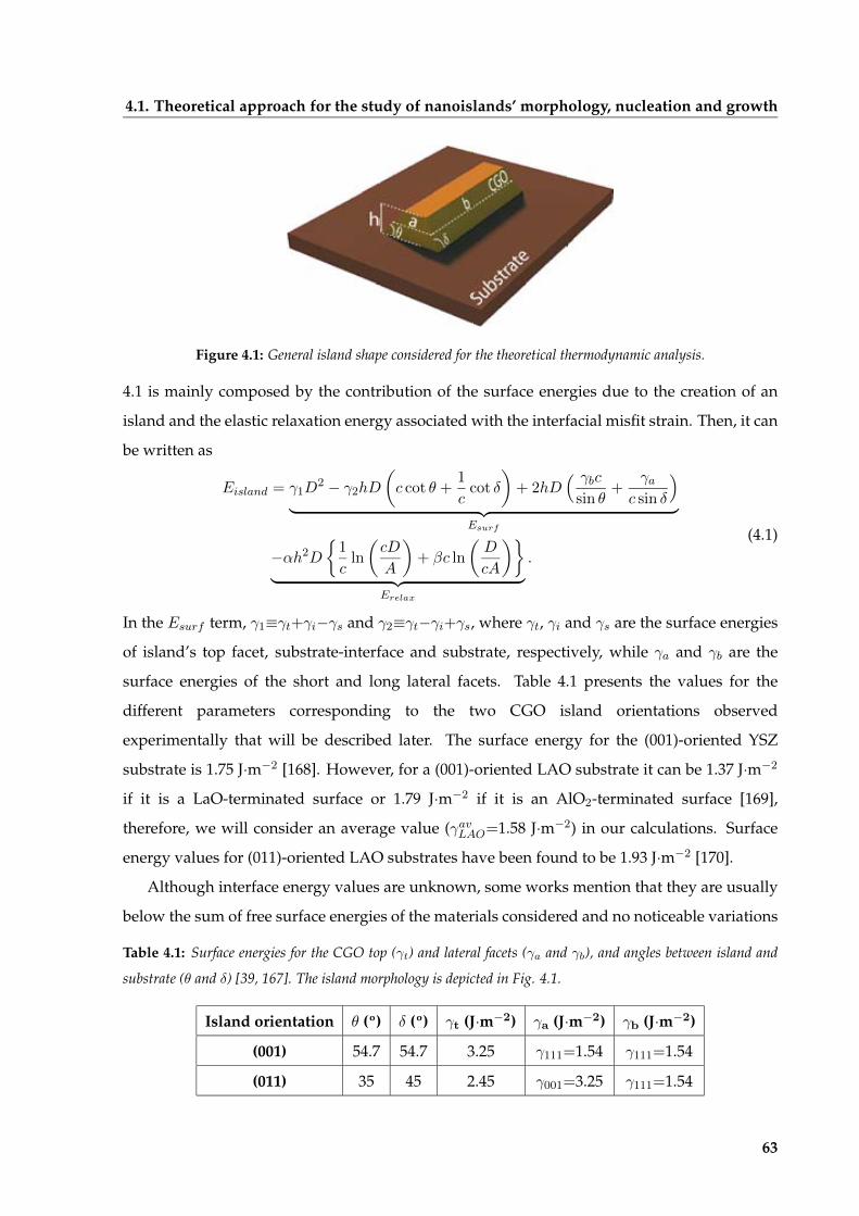
4.1. Theoretical approach for the study of nanoislands’ morphology, nucleation and growth
Figure 4.1: General island shape considered for the theoretical thermodynamic analysis.
4.1 is mainly composed by the contribution of the surface energies due to the creation of an
island and the elastic relaxation energy associated with the interfacial misfit strain. Then, it can
be written as
Eisland = γ1D2−γ2hD
(c cot θ +
1
ccotδ
)+ 2hD
( γbcsin θ
+γa
c sinδ
)︸ ︷︷ ︸
Esurf
−αh2D
1
cln
(cD
A
)+ βc ln
(D
cA
)︸ ︷︷ ︸
Erelax
.
(4.1)
In the Esurf term, γ1≡γt+γi−γs and γ2≡γt−γi+γs, where γt, γi and γs are the surface energies
of island’s top facet, substrate-interface and substrate, respectively, while γa and γb are the
surface energies of the short and long lateral facets. Table 4.1 presents the values for the
different parameters corresponding to the two CGO island orientations observed
experimentally that will be described later. The surface energy for the (001)-oriented YSZ
substrate is 1.75 J· m−2 [168]. However, for a (001)-oriented LAO substrate it can be 1.37 J· m−2
if it is a LaO-terminated surface or 1.79 J· m−2 if it is an AlO2-terminated surface [169],
therefore, we will consider an average value (γavLAO=1.58 J· m−2) in our calculations. Surface
energy values for (011)-oriented LAO substrates have been found to be 1.93 J· m−2 [170].
Although interface energy values are unknown, some works mention that they are usually
below the sum of free surface energies of the materials considered and no noticeable variations
Table 4.1: Surface energies for the CGO top (γt) and lateral facets (γa and γb), and angles between island and
substrate (θ and δ) [39, 167]. The island morphology is depicted in Fig. 4.1.
Island orientation θ (º) δ (º) γt (J· m−2) γa (J· m−2) γb (J· m−2)
(001) 54.7 54.7 3.25 γ111=1.54 γ111=1.54
(011) 35 45 2.45 γ001=3.25 γ111=1.54
63

4. Interfacial Ce0:9Gd0:1O2y oxide nanostructures: a thermodynamic and kinetic study
should be expected [131]. Nevertheless, the influence of interface might not be negligible in
certain cases, and consequently, it will be evaluated later.
The Erelax term has been derived following the work from Tersoff and Tromp [139]
explained in section 3.1. However, a generalization of Eq. 3.3 was developed in a previous
work by Gibert et al. [166] with the inclusion of a dimensionless factor accounting for the
stress anisotropy , as well as a A coefficient which considers the contribution of the edges
and depends on island’s height (A=kh) [39, 137]. A values have been considered to be
between 0.5 and 5.5 nm. Moreover, =δ2(1Ψ)=βν with δ being the island stress tensor, Ψ and
ν the Poisson ratio and shear modulus of the substrate, respectively. The value of the stress
tensor can be estimated considering δ〈Y " [137], where Y is the Young modulus and " the
lattice mismatch. Common perovskite values for this parameters have been considered, i. e.
Y =200 GPa, ν=80 GPa and Ψ=0.3 [94, 171].
This theoretical development will be used later as a mean to evaluate the thermodynamic
contribution of coarsening from the minimization of the energy density [39, 139]
EislandV
= 1
h 2
D
∫c cot +
1
ccot
]+
2
D
bcsin
+ a
c sin
| z
Esurf=V
hD
︷1
cln
∫cD
A
]+ c ln
∫D
cA
]︸| z
Erelax=V
;
(4.2)
were the volume of a nanoisland has been defined in terms of the effective diameter (V=hD2).
Following a similar development as the one presented in Chapter 3, we can analyze the
nucleation stage. It should be noted that at the very early stage of nucleation where the critical
size is considerably small (few nanometers), the main contribution to the overall energy of an
island will come from the surface energy term in Eq. 4.1 which can be written as [51]
Esurf = D2 + hD; (4.3)
where t + i s and =2 bc csc + ac
1 csc ( t i + s)
c cot + c1 cot
.
Accordingly, the variation in Gibbs free energy for this particular case is
G(D) = hD2
Ψν+ D2 + Dh; (4.4)
where Ψ is the unit cell volume, and ν is the change in chemical potential between the
epitaxial and amorphous/nanocrystalline state and has been defined to be positive. Then, the
energy barrier and critical size for the nucleation of a CGO nanoisland are
G = 2h2
4hν+
(4.5a)
64

4.2. Shape selection of nanostructures
and
D =h
2h ν+
; (4.5b)
respectively.
Although the contribution of strain to the island’s energy has only been considered in the
Erelax term, its influence on surface and interface energies could be strong enough to modify
its shape or nucleation barrier. Thus, we will evaluate its effect too.
4.2 Shape selection of nanostructures
In this section two different examples of epitaxial CGO nanostructures will be described. On
the one hand, we will investigate the growth of isotropic islands on (001)-oriented YSZ and
LAO substrates in oxidizing atmosphere. On the other hand, anisotropic nanowires will be
grown on (011)-oriented LAO substrates in O2, while it will be shown that it is possible to
grow other anisotropic morphologies on (001)LAO substrates if a reducing Ar-H2 annealing
atmosphere is used instead. In particular, we will study and compare in detail the stable
shape, structure and oxidation state of these nanostructures. The influence of biaxial strain,
and surface and interface energies in the stabilization of islands’ shape will also be analyzed
from a theoretical point of view. Finally, some hints about islands’ kinetic evolution will be
derived using thermodynamic calculations.
4.2.1 Isomorphic CGO nanostructures
The formation of isotropic CGO nanoislands have been observed on two different single crystal
substrates, (001)-oriented YSZ and LAO (Fig. 4.2), during high temperature (〈1000 ºC) thermal
treatments by RTA in oxygen atmosphere. As we can see from Fig. 4.2a, CGO islands grow on
(001)YSZ substrates with a square-shaped base oriented 45º from the h100i substrate axes, while
in Fig. 4.2b islands’ shape is aligned with the h100i LAO substrate axes.
In the case of YSZ substrates, both materials (YSZ and CGO) have a fluorite structure and
are completely compatible from the chemical point of view. A cube on cube disposition of
the structures is to be expected (Fig. 4.3a). Apart from that, the theoretical compressive lattice
mismatch "〈5% (aY SZ=5.145 A and aCGO=5.413 A) between the two structures is sufficiently
high to lead to the formation of nanoislands.
High-resolution TEM analysis of nanoislands (Figs. 4.3b-d) shows that their shape consists
of a truncated pyramid. This shape has already been observed before on CGO islands grown
65

4. Interfacial Ce0:9Gd0:1O2y oxide nanostructures: a thermodynamic and kinetic study
(a) (b)
0.25 µm 0.25 µm
[100]YSZ
[010
]YSZ
[100]LAO
[010
]LA
O
Figure 4.2: Isotropic CGO nanoislands on (001)-oriented single crystal (a) YSZ and (b) LAO substrates. Both
AFM images correspond to samples annealed at 1000 ºC, 20 ºCs1 for 15 min in O2.
on other substrates [39, 51], as well as films deposited on YSZ by sputtering where islands were
generated due to fluctuations created by strain [172]. Other oxides grown on YSZ such as In2O3
nanodots by MBE [173] or LSMO nanoislands by CSD [35] have shown the same morphology
as well. In some thin films, faceted grains with the same shape can also be identified, as we
will see in chapter 5.
As it can be seen from Fig. 4.3b, the top facet corresponds to the (001) plane and the
arrangement of YSZ and CGO lattices is cube on cube with the configuration
(001)CGO[100]k(001)YSZ[100] (Fig. 4.3d). Regarding lateral facets, Fig. 4.3b seems to indicate
a (011) orientation for the lateral facets. However, there are two possibilities for nanoislands
on YSZ to display lateral (011) facets when samples are cut along substrate axes as shown in
Figs. 4.3e and f. Since the specimen was cut parallel to substrate axes during TEM sample
preparation and AFM images (Fig. 4.2a) show that CGO islands display a 45º-rotated cubic
shape with respect to YSZ axes when seen from above, we can deduce that sample
preparation causes a misleading perspective and lateral facets of CGO nanoislands on YSZ
have the lowest surface energy configuration of CGO, i. e. the (111) orientation (Table 4.1), as
observed previously in other cases [11, 51, 166].
The degree of relaxation of these islands can be evaluated by the separation between misfit
dislocations which for a fully relaxed bulk system is calculated from [174]
S =
!b "; (4.6)
where!b =(a=2)
ph2 + k2 + l2 is the modulus of the dislocation Burgers vector and " is the
lattice mismatch. In this case,!b =1
2 h100i gives a theoretical separation of 〈5.4 nm, close to
the experimental value 〈5 nm (Fig. 4.3c). This islands seem to be fully relaxed even for small
sizes as it is shown in Fig. 4.3d.
66

4.2. Shape selection of nanostructures
(a) (b) (c)
[100]CGO||[100]YSZ
[001
]CG
O||[
001]
YSZCe/Gd
Zr/Y
O
(001)
CGO
YSZ[001]
CGO
YSZ
T T T
5 nm5 nm
CGO[001]
(d) (e) (f)
(011
) (011)
(200)CGO[010]//YSZ[010]
CGO[100]//YSZ[100]
CG
O[0
01]/
/YSZ
[001
]
(020)
(1-10)(111)
[100]CGO||[100]YSZ
[100
]CG
O||[
100]
YSZ (011)
(011
) (011)
[100]CGO||[100]YSZ
[100
]CG
O||[
100]
YSZ
(011)
(011
) (011)
Figure 4.3: (a) Solid sphere model showing the matching between CGO and YSZ structures along the
[010]CGO | | [010]Y SZ direction. Isomorphic CGO nanoislands grown on (001)YSZ. (b) High-resolution TEM
depicting the parallelepipedic shape of a single island. (c) Inverse-filtered image of (b) generated with the (00l)
reflections of CGO and YSZ, and depicting island dislocations every∼5 nm. (d) Fourier Transform of (b) showing
the cube on cube arrangement of CGO and YSZ lattices, as well as the epitaxial relationship between island and
substrate. (e) 45º-rotated and (f) non-tilted island solid sphere models sketching lateral facets and their relation
with TEM sample preparation.
On the other hand, the case of CGO islands grown on (001)LAO is particularly interesting
because, unlike the previous case, both crystallographic structures are atomically different
(fluorite on perovskite). Even though the island shape is the same, and a truncated pyramid
with (111) lateral facets and a (001) top facet is observed (Fig. 4.4a), the CGO lattice sits 45º
rotated with respect to that of LAO, i. e. (001)CGO[110]‖(001)LAO[100], as shown in Fig. 4.4b
and already reported by Gibert et al. [51]. The particular disposition of CGO provides a real
theoretical matching of ε=(as−d110) /d110∼−1%, where d110=3.827 A is the interplanar
separation of (110) planes of the CGO fluorite structure. Gibert et al. pointed out [11, 116] that
such interfaces are very likely to present oxygen vacancies since it seems that there is not
enough room to arrange oxygen atoms of both structures as we schematically represented in
Fig. 4.4c. In this case, the mean separation of dislocations for islands grown on LAO is larger
67

4. Interfacial Ce0.9Gd0.1O2−y oxide nanostructures: a thermodynamic and kinetic study
(c)(a) (b)
(111
) (111)
(001)CGO[001]
LAO[001]
(002)
(111)
(220)
(101)
(200)
CG
O[0
01]/
/LA
O[0
01]
CGO[-110]//LAO[010]
CGO[110]//LAO[100]Ce/Gd
O
Al
[110]CGO||[100]LAO
[001
]CG
O||[
001]
LA
O
Vacancy
Figure 4.4: Isomorphic CGO nanoislands grown on (001)LAO. (a) High-Angle Anular Dark Field Scanning
Transmission Electron Microscopy (HAADF-STEM) images depicting the parallelepipedic shape of a single
nanoisland. (b) Fourier Filtered image of (a) showing the epitaxial relationship between island and substrate.
(c) Solid sphere model sketching the interface between CGO and LAO lattices along the [110]CGO | | [100]LAO
in-plane direction.
than their size in most cases S∼38 nm (from Eq. 4.6 and assuming∣∣∣−→b ∣∣∣=1
2 〈110〉)). Therefore,
the presence of oxygen vacancies and its distribution could have an important contribution to
strain relaxation as we will see later.
The isomorphic islands described so far have been obtained in O2 atmosphere. However,
it is also possible to achieve such morphology on (001)LAO when annealing at T∼800 ºC in
Ar/5%-H2 and short annealing times [51]. If higher temperatures or longer annealing times are
used, a transformation from (001)CGO nanodots to (011)CGO nanowires occurs. This transition
is associated to specific thermodynamic and kinetic situations as it will be explained later in
section 4.3.5.
4.2.2 Inducing shape anisotropies
Besides the formation of isotropic nanoislands, it is also possible to obtain islands with one of
their in-plane directions larger than the other, i. e. nanowires, by changing substrate
orientation from (001)- to (011)-LAO (Fig. 4.5a) or growth conditions, i. e. annealing
atmosphere from O2 to Ar-H2 and going to high enough temperature (∼1000 ºC) as it has been
demonstrated by Gibert et al. using slow conventional furnace annealing [52]. Although we
have focused on the study of nanowires induced due to a modification of the substrate
orientation, we reproduced the latter case using RTA treatments for completeness and
comparison (Fig. 4.5b). Both nanowires shown in Fig. 4.5 were grown by RTA at 1000 ºC, 20
ºC· s−1 for 15 min. Besides the different LAO orientations used, nanowires from Fig. 4.5a and
4.5b were grown in O2 and Ar-H2, respectively. The reason why in Fig. 4.5a there are parallel
68

4.2. Shape selection of nanostructures
nanowires whereas in Fig. 4.5b they are orthogonal will be explained in section 4.2.5.
(a) (b)
[0-11]LAO
[010
]LA
O
[100]LAO
[010
]LA
O
0.25 µm 0.25 µm
Figure 4.5: Anisotropic CGO nanowires on (a) (011)- and (b) (001)-oriented single crystal LAO substrates. Both
AFM images correspond to samples annealed at 1000 ºC, 20 ºCs1 for 15 min in O2 and Ar-H2, respectively.
Cross-sectional HAADF-STEM images of nanowires grown on LAO(011) (Figs. 4.6a and d),
and corresponding power spectrum analyses (Figs. 4.6b and e) show that these nanostructures
have a trapezoidal-like shape with a (011)-oriented top facet and (111) lateral facets along the [0-
11]CGOk[100]LAO direction, and (010) lateral facets along the [100]CGOk[0-11]LAO direction.
In addition, it is clearly seen that in-plane axes of CGO and LAO lattices are rotated 90º which
gives a theoretical compressive lattice mismatch "=dLAOhkl dCGOhkl
=dCGOhkl 〈1% (where dhkl
are the interplanar distances of both CGO and LAO structures) in both directions, i. e. strain is
isotropic as in the case of (001)CGO nanoislands on (001)LAO. Then, the shape anistropy will
be driven by different energies of lateral facets as we will see from thermodynamic analyses.
A solid spheres model of the interface in both in-plane directions (Figs. 4.6c and f) shows
that matching between CGO and LAO cation lattices is, indeed, good. However, some
vacancies should be expected at the interface due to overlapping of oxygen atoms between
both structures. Although the lattice mismatch is low, the mean separation of dislocations
should be between 40 and 50 nm, similarly to what has been observed for isotropic (001)
nanodots on (001)LAO. This value is larger than most nanowires’ width but not their length;
however, HAADF-STEM images analyzed were not long enough to find any dislocations.
Since the theoretical mismatch is low ("〈1%), the formation of oxygen vacancies at the
interface could act as a strain relaxation mechanism, reducing the driving force towards misfit
dislocation formation.
As we said previously, (011)CGO nanowires have been already grown on (001)LAO
substrates in Ar-H2 by Gibert et al. Although, they present the same lateral facets like those
grown on (011)LAO, i. e. (111) facets along the long direction and (011) facets along the short
69

4. Interfacial Ce0.9Gd0.1O2−y oxide nanostructures: a thermodynamic and kinetic study
Figure 4.6: Analysis of (011)CGO nanowires on (011)LAO. (a) Cross-sectional HAADF-STEM image, (b) Power
spectrum (Fast Fourier Transform or FFT) analysis of (a), and (c) solid spheres model of the interface along the [0-
11]CGO‖[100]LAO direction. (d) Cross-sectional image, (e) power spectrum analysis of (d), and (f) solid spheres
model of the interface along the [100]CGO‖[0-11]LAO direction.
direction, the arrangement between them and the (001)LAO substrate is substantially
different, i. e. the in-plane alignment consists of a direction ([0-11]CGO‖[010]LAO) with a low
compressive mismatch of −1% and another direction ([010]CGO‖[100]LAO) with a large
tensile mismatch of 5%. This particular disposition led to a matching of 2 CGO unit cells with
3 LAO unit cells (following a domain matching epitaxy (DME) model [175]) and,
consequently, to the presence of an extremely high density of misfit dislocations [52].
4.2.3 Tuning oxygen stoichiometry of nanostructures
In the previous section, it has been repeatedly stated that oxygen vacancies are likely to be
present in the structure of CGO due to the particular arrangement of nanostructures at the
interface with substrates. X-ray photoelectron spectroscopy (XPS) is a good technique to
evaluate the oxidation state, even though it tends to overestimate the amount of Ce3+ [176]; it
must be assumed that only around 20-30 % of the top part of the sample is being sensed due
to the known limitations in the electrons mean free path and thickness. Previous XPS
measurements performed on CGO nanodots grown by CSD in an oxygen atmosphere showed
70

4.2. Shape selection of nanostructures
that they have an extremely high amount of oxygen vacancies, i. e. a ratio
Ce3+/Ce4+(%) 〈40/60 [51].
Measurements of oxygen vacancies in CeO2 nanoparticles through STEM-EELS suggest
that vacancies are mainly located at their surface [177]. Similar experiments have been carried
out on CGO nanodots indicating a large amount of Ce3+ ions along them, i. e. high content of
oxygen vacancies. Nevertheless, conclusive results could not be extracted because it was
found that either sample preparation by PIPS or interaction with the electron beam during
imaging may influence the oxygen content of cerium oxide as reported in [178]. Song et al.
also found presence of oxygen vacancies by STEM-EELS at the interface of CeO2 thin-films on
(111)YSZ grown by PLD, although their preparation procedure was the same as ours [179].
An alternative method supporting the presence of oxygen vacancies at the interface has
been proposed by Solovyov et al. from the analysis of reciprocal space maps obtained using
synchrotron X-ray diffraction [180]. Examination of symmetric and asymmetric reflections
allowed them to deduce that islands smaller than 40 nm are compressed in the out-of-plane
direction and present a large in-plane tensile strain. Modeling of reciprocal space maps was
done considering that strain depends linearly on island’s size. This is only true if oxygen
stoichiometry is inhomogeneous along islands and vacancies concentration is slightly larger at
the interface. Actually, this assumption could also be consistent with high ionic conductivity
values such as those reported by Garcia-Barriocanal for YSZ/STO heterostructures [73] that
have been attributed to the presence of large amounts of oxygen vacancies at the
fluorite/perovskite interface.
This phenomenon is not exclusive of isotropic islands, but it could play a vital role in the
structural relaxation of nanowires. Gibert et al. also evaluated the oxygen stoichiometry of
(011)CGO nanowires grown on (001)LAO in Ar-H2 atmosphere, and reported a larger amount
of Ce3+ ions (Ce3+/Ce4+(%)=65=35) [51], which is translated to an enhanced presence of
vacancies with respect to nanodots grown in O2. Despite the Ar-H2 annealing atmosphere
contributes to the formation of oxygen vacancies, the complicated arrangement of (011)CGO
nanowires on (001)LAO, which are only stabilized on this substrate under Ar-H2, may
promote oxygen deficiencies at the interface as Gibert et al. proposed [11]. The large content
of oxygen vacancies could lead to an enhanced kinetic evolution of these nanowires as we will
see later.
The oxygen stoichiometry of (011)CGO nanowires grown on (011)LAO in O2 has also been
evaluated by XPS as described in section A.1.2. Fig. 4.7 depicts the Ce 3d core level spectra
71

4. Interfacial Ce0.9Gd0.1O2−y oxide nanostructures: a thermodynamic and kinetic study
with a deconvolution of the individual contributions. The resulting integration of the
individual peak areas is reported in Table 4.2. The overall ratio between Ce3+ and Ce4+ ions is
calculated by summation of the peaks colored in green and red, respectively, which reveal a
ratio equivalent to that observed for isotropic nanodots, i. e. Ce3+/Ce4+(%)∼40/60. In spite
of these results, XPS measurements of 20 nm-thick CGO thin-films in our group have shown
that the amount of Ce3+ ions is significantly smaller, i. e. ∼0% in O2 [108]. Probably this could
change if ultrathin films (∼5 nm) are measured. Consequently, we hypothesize that
nanoislands dimensions together with their particular arrangement with substrates may
contribute to a great extent defining the amount of oxygen inside the CGO structure.
The presence of oxygen vacancies in 3D systems has already been measured by different
methods such as EELS or XPS for example in CeO2 nanoparticles. They have found that
small-sized ones are fully reduced, i. e. 100% of Ce3+ ions, while oxygen vacancies in larger
nanoparticles are distributed along their surface [176, 177, 181]. Several phenomena could
explain this event such as the larger surface-to-volume ratio of these systems compared to
thin-films allowing oxygen to deplete faster or chemical terminations different than that of
920 910 900 890 8800
200
400
600
CPS
Binding Energy (eV)
v0u0
vu
v1
u1 v2u2u3
v3
Figure 4.7: XPS Ce 3d core level spectra of (011)CGO nanowires grown on (011)LAO in O2 atmosphere at 1000
ºC, 20 ºC· s−1 for 5 min. The fitted components shadowed in green correspond to Ce3+ ions, while those shadowed
in red to Ce4+ ions.
Table 4.2: Quantification of the individual peak areas extracted from Fig. 4.7 and normalized to the sum of all
peak areas.
v0 (%) v (%) v1 (%) v2 (%) v3 (%) u0 (%) u (%) u1 (%) u2 (%) u3 (%)
3.97 15.01 15.33 8.81 11.81 3.59 13.58 13.88 7.98 6.04
72

4.2. Shape selection of nanostructures
(111)facets which have shown a greater probability to form oxygen vacancies [181].
Nevertheless, it is still an open issue requiring further investigation.
Additional details on how the XPS measurements and data analysis is performed can be
found in Appendix A.1.2. The influence of nanowires shape on their kinetic evolution will be
discussed in sections 4.2.4 and 4.4.
4.2.4 Thermodynamic stability of nanoislands morphology
From the beginning, CGO isotropic and anisotropic nanostructured systems do not fulfill the
wetting condition since γCGO+γi>γs, and this supports the experimental evidence that
nanoislands are the preferred morphology. In addition, the stability and final shape of
different nanostructures can be verified using the thermodynamic model explained in section
4.1, where the strain relaxation energy is considered too. Initially, the unknown contribution
of the interface energy γi has not been considered for simplicity, although its possible effect
will be evaluated as well later on.
Fig. 4.8a shows the dependence of Etotal, Esurf and Erelax on the lateral aspect ratio c for a
(001)CGO nanoisland (D=20 nm and h=7 nm) on a (001)LAO substrate. All energy
contributions are isotropic around c=1, and Etotal presents a minimum at that point which
proves that the lowest energy configuration is when the island’s shape is isomorphic. The
parameters used for the calculations are α=107 J· m−3, β=1 and A between 0.5 and 5 nm; the
surface energy of the substrate was considered to be γavLAO=1.58 J· m−2. The effect of the
(a) (b) (c)
0.1 1 10
6
8
10
12
c (log)
E (
10-4 p
J)
EYSZ
ELAOLa-O
ELAOAl-O
00 10 20 30 4-2-101234
E/V
(10
-7 p
J·nm
-3)
D=(ab)0.5 (nm)
(E/V)YSZ
(E/V)LAOLa-O
(E/V)LAOAl-OEtotal
Esurf
Erelax0789101112
0.1 1 10c (log)
E (
10-4 p
J)
Figure 4.8: Energy calculations for isomorphic CGO nanoislands. (a) Total (—), surface (- - -) and relaxation
(- - -) energies as a function of the lateral aspect ratio c for (001)CGO islands on (001)LAO. Parameters used
are D=20 nm, h=7 nm, α=107 J· m−3, β=1 and A between 0.5 and 5 nm. (b) Total energy as a function of c,
and (c) energy density (E/V ) as a function of the effective diameter D of nanodots on YSZ (—), AlO2- (—) and
LaO-terminated LAO (—) substrates. The red-dashed (- - -) curve is the one obtained for γavLAO=1.58 J· m−2.
73

4. Interfacial Ce0:9Gd0:1O2y oxide nanostructures: a thermodynamic and kinetic study
surface energy of the substrate has been evaluated in Fig. 4.8b, where the total energy of an
island is higher for a LaO-terminated LAO substrate ( LaOLAO =1:37 Jm2) than for an
AlO2-terminated one ( AlOLAO =1:79 Jm2). Usually, we can expect that our LAO substrates do
not have a unique termination, therefore, there is a region where the island energy should be
(colored area in Fig. 4.8b). For simplicity, we took the mean value of (001)LAO surface
energies (red-dashed curve). Even though the surface energy of YSZ substrate ( Y SZ=1:75
Jm2) is similar to AlOLAO , the energy for an island grown on YSZ is lower due to a larger
strain relaxation energy ("CGOkY SZ>"CGOkLAO).
In order to evaluate if there is a stable maximum size for these nanodots or, on the contrary,
there is a tendency towards coarsening; we have calculated the change in energy density E=V
(Eq. 4.2) as the effective diameter D increases. From Fig. 4.8c, it is clearly seen that the E=V
curves present a minimum for a D=1020 nm. This means that isotropic CGO nanoislands
grown on YSZ and LAO substrates will have a stable size, and consequently, a limited kinetic
evolution as it will be shown later. The energy density curves exhibit the same behaviour
observed in Fig. 4.8b due to substrate surface energies and strain.
The stability of nanowires have been analyzed as well, again without considering the
contribution of i. Figs. 4.9a and b present the dependence of Etotal, Esurf and Erelax on the
lateral aspect ratio c for (011)CGO nanowires on (011)- and (001)-oriented LAO substrates,
respectively. In both cases, it can be observed that the contribution of surface energy is
anisotropic (c>1), while the relaxation energy is isotropic in the former case and anisotropic in
the later. This difference in the strain relaxation energy is due to the particular arrangement of
(a)
0.1 1 10-60-40-2002040
Erelax
Etotal
E (1
0-4 p
J)
c (log)
Esurf
(b)
-100
102030
0.1 1 10
Erelax
Etotal
E (1
0-4 p
J)
c (log)
Esurf
Figure 4.9: Energy calculations for anisotropic CGO nanowires. Total (—), surface (- - -) and relaxation (- - -)
energies as a function of the lateral aspect ratio c for (a) (011)CGO nanowires on (011)LAO, and (b) (011)CGO
nanowires on (001)LAO. Parameters used are D=40 nm, h=4 nm, =108 Jm3, =1 (a) or =5 (b), and
A=4:4 nm.
74
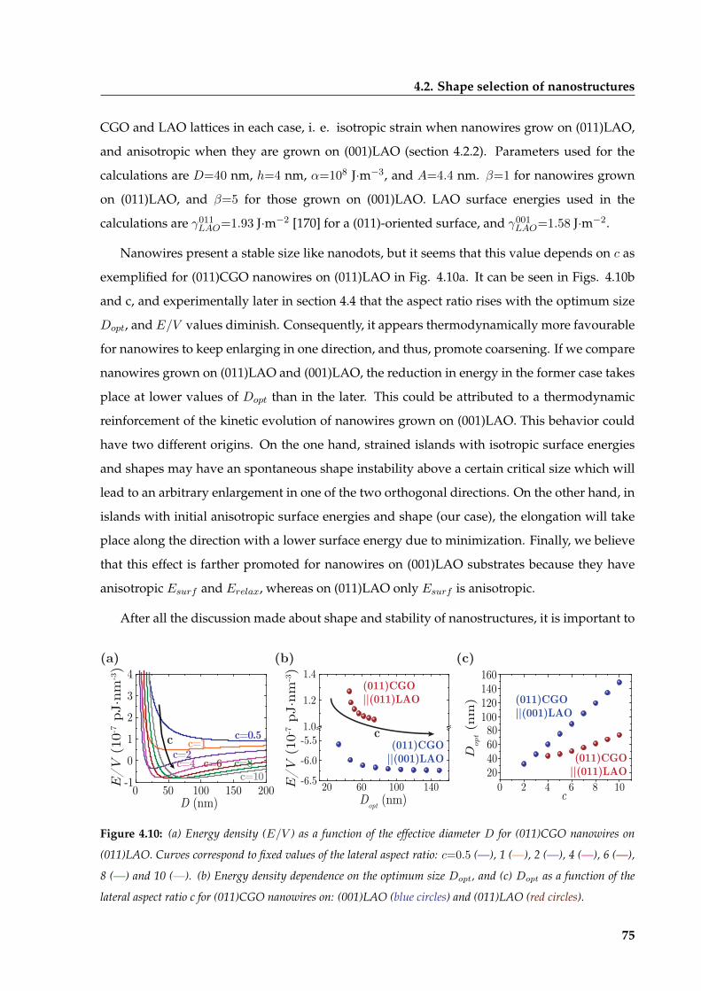
4.2. Shape selection of nanostructures
CGO and LAO lattices in each case, i. e. isotropic strain when nanowires grow on (011)LAO,
and anisotropic when they are grown on (001)LAO (section 4.2.2). Parameters used for the
calculations are D=40 nm, h=4 nm, =108 Jm3, and A=4:4 nm. =1 for nanowires grown
on (011)LAO, and =5 for those grown on (001)LAO. LAO surface energies used in the
calculations are 011LAO=1:93 Jm2 [170] for a (011)-oriented surface, and 001
LAO=1:58 Jm2.
Nanowires present a stable size like nanodots, but it seems that this value depends on c as
exemplified for (011)CGO nanowires on (011)LAO in Fig. 4.10a. It can be seen in Figs. 4.10b
and c, and experimentally later in section 4.4 that the aspect ratio rises with the optimum size
Dopt, and E=V values diminish. Consequently, it appears thermodynamically more favourable
for nanowires to keep enlarging in one direction, and thus, promote coarsening. If we compare
nanowires grown on (011)LAO and (001)LAO, the reduction in energy in the former case takes
place at lower values of Dopt than in the later. This could be attributed to a thermodynamic
reinforcement of the kinetic evolution of nanowires grown on (001)LAO. This behavior could
have two different origins. On the one hand, strained islands with isotropic surface energies
and shapes may have an spontaneous shape instability above a certain critical size which will
lead to an arbitrary enlargement in one of the two orthogonal directions. On the other hand, in
islands with initial anisotropic surface energies and shape (our case), the elongation will take
place along the direction with a lower surface energy due to minimization. Finally, we believe
that this effect is farther promoted for nanowires on (001)LAO substrates because they have
anisotropic Esurf and Erelax, whereas on (011)LAO only Esurf is anisotropic.
After all the discussion made about shape and stability of nanostructures, it is important to
(a) (b) (c)
0 50 100 150 200-1
0
1
2
3
4
D (nm)
E/V
(10
-7 p
J·nm
-3)
c=0.5 c=1
c=2 c=4 c=6 c=8
c=10
c
0 8 10
20406080
100120140160
Dop
t (nm
)
2 4 6c
(011)CGO||(011)LAO
(011)CGO||(001)LAO
20 60 100 140-6.5
-6.0
-5.51.0
1.2
1.4
(011)CGO||(011)LAO
(011)CGO||(001)LAO
E/V
(10
-7 p
J·nm
-3)
c
Dopt (nm)
Figure 4.10: (a) Energy density (E=V ) as a function of the effective diameter D for (011)CGO nanowires on
(011)LAO. Curves correspond to fixed values of the lateral aspect ratio: c=0:5 (—), 1 (—), 2 (—), 4 (—), 6 (—),
8 (—) and 10 (—). (b) Energy density dependence on the optimum size Dopt, and (c) Dopt as a function of the
lateral aspect ratio c for (011)CGO nanowires on: (001)LAO (blue circles) and (011)LAO (red circles).
75

4. Interfacial Ce0:9Gd0:1O2y oxide nanostructures: a thermodynamic and kinetic study
highlight the influence of parameters such as and which include the influence of
isotropic/anisotropic strain and surface energies. In fact, a phase-like diagram can be built
considering distinct values of both parameters as reported by Gibert et al. [166] and
reproduced in Fig. 4.11 for completeness. The parameters used to build this diagram are
D=50 nm and h=4 nm, although similar diagrams can be obtained for other values of D and
h. From Fig. 4.11, different situations can be identified. When values are at least two orders
of magnitude larger than 0=107 Jm3 and −1 (diamond-like region). Islands should have
lateral dimensions with a>b. This is not in agreement with the formalism used where b>a,
and therefore, it is a very unlikely situation. Having values of <1 would imply that for
islands with an anisotropic biaxial strain, those values will be inverted. For instance, if we
consider the case of (011)CGO nanowires on (001)LAO which are known to have dissimilar
values of strain, the in-plane direction with large strain should be the [0-11]CGOk[100]LAO
instead of the experimentally observed [010]CGOk[100]LAO. Furthermore, if =0, the
coherence of nanostructures along one of the in-plane directions would break. When is
rather small (striped green region), the contribution of Esurf will dominate over the Erelax
term, and nanostructures elongation will be promoted endlessly. However, this is not the case
for the nanostructures analyzed, since thermodynamic calculations show a dependence
between their lateral aspect ratio and optimum size, which will also be demonstrated
experimentally in section 4.4. If and values are large (region with red vertical lines), the
relaxation term dictates the behavior of islands’ energy and the island shape is detached from
103
101
10-1
10-310-3 10-2 10-1
10-2
100
102
100 101 102 103
α/α 0
β
c=1
Figure 4.11: Phase diagram depicting different in-plane anisotropic shape regions as a function of and values.
The black-dashed line (- - -) indicates the region of isotropic nanostructures. Parameters used are D=50 nm and
h=4 nm. Adapted from [166].
76
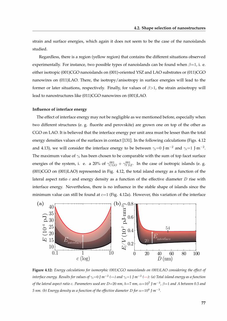
4.2. Shape selection of nanostructures
strain and surface energies, which again it does not seem to be the case of the nanoislands
studied.
Regardless, there is a region (yellow region) that contains the different situations observed
experimentally. For instance, two possible types of nanoislands can be found when β=1, i. e.
either isotropic (001)CGO nanoislands on (001)-oriented YSZ and LAO substrates or (011)CGO
nanowires on (011)LAO. There, the isotropy/anisotropy in surface energies will lead to the
former or later situations, respectively. Finally, for values of β>1, the strain anisotropy will
lead to nanostructures like (011)CGO nanowires on (001)LAO.
Influence of interface energy
The effect of interface energy may not be negligible as we mentioned before, especially when
two different structures (e. g. fluorite and perovskite) are grown one on top of the other as
CGO on LAO. It is believed that the interface energy per unit area must be lesser than the total
energy densities values of the surfaces in contact [131]. In the following calculations (Figs. 4.12
and 4.13), we will consider the interface energy to be between γi=0 J· m−2 and γi=1 J· m−2.
The maximum value of γi has been chosen to be comparable with the sum of top facet surface
energies of the system, i. e. a 20% of γ001CGO + γ001
Y SZ . In the case of isotropic islands (e. g.
(001)CGO on (001)LAO) represented in Fig. 4.12, the total island energy as a function of the
lateral aspect ratio c and energy density as a function of the effective diameter D rise with
interface energy. Nevertheless, there is no influence in the stable shape of islands since the
minimum value can still be found at c=1 (Fig. 4.12a). However, this variation of the interface
(a) (b)
0.1 1 1010152025303540
E (
10-4 p
J)
c (log)
Einterface
0 20 40 60 80 100
0.2
0.4
0.6
0.8
E/V
(10
-7 p
J·nm
-3)
D (nm)
Einterface
54
20
Figure 4.12: Energy calculations for isomorphic (001)CGO nanoislands on (001)LAO considering the effect of
interface energy. Results for values of γi=0 J· m−2 (—) and γi=1 J· m−2 (—): (a) Total island energy as a function
of the lateral aspect ratio c. Parameters used are D=20 nm, h=7 nm, α=107 J· m−3, β=1 and A between 0.5 and
5 nm. (b) Energy density as a function of the effective diameter D for α=108 J· m−3.
77

4. Interfacial Ce0.9Gd0.1O2−y oxide nanostructures: a thermodynamic and kinetic study
energy from 0 to 1 J· m−2 results in a drastic rise of the maximum island size from 20 to∼50 nm
(Fig. 4.12b).
The same variation of γi for nanowires moves the total energy to higher values as it has
been observed for nanodots, but contrarily to them, there is a small shift of the lateral aspect
ratio c to low values as illustrated in Fig. 4.13a. Similarly to nanodots, the energy density E/V
experiences a displacement to higher values, and the optimum diameter increases (Fig. 4.13b).
Consequently, although the exact values of interface energies are unknown, its effect may be
really significant and should be considered.
(a) (b)
0.1 1 10
-25
0
25
50
75
100
E (
10-4 p
J)
c (log)
Einterface
Einterface
(011)CGO||(011)LAO
(011)CGO||(001)LAO
1.9
2.73.7
4.4
0 50 100 150 200-8-6-4-2024
E/V
(10
-7 p
J·nm
-3)
D (nm)
Einterface
Einterface
(011)CGO||(011)LAO
(011)CGO||(001)LAO
67
5066
59
Figure 4.13: Energy calculations for anisotropic (011)CGO nanowires on (001)- and (011)-LAO substrates
considering the effect of interface energy. Results for values of γi=0 J· m−2 (— and — curves) and γi=1 J· m−2
(— and — curves): (a) Total island energy as a function of the lateral aspect ratio c. Parameters used are D=40
nm, h=5 nm, α=108 J· m−3 and A=5.5 nm. β=1 for nanowires grown on (011)LAO and β=25 when grown on
(001)LAO. (b) Energy density as a function of the effective diameter D for c=4.
4.2.5 Broken degeneracy of CGO nanowires on (011)LAO
Two possible arrangements have been obtained for nanowires, i. e. parallel or orthogonal,
depending on substrate orientation as shown in Fig. 4.5. Remember that nanowires on
(011)LAO present a low strain configuration of −1% along both in-plane directions, i. e.
[100]CGO‖[0-11]LAO and [0-11]CGO‖[100]LAO. On the other hand, nanowires obtained on
(001)LAO have a low strain of -1% in the [0-11]CGO‖[100]LAO direction, whereas it is ∼5%
along the [010]CGO‖[100]LAO direction.
Besides parallel nanowires, we observed in Fig. 4.5a the presence of small islands which
resemble to nanodots. In order to unveil the structural arrangement of such features we
performed High Resolution Transmission Electron Microscopy (HRTEM) and HAADF-STEM
78

4.2. Shape selection of nanostructures
(a)
10 nm
(011) CGO
(011) LAO
(022) (011)
(0-20)(-100)
(0-22)
(011)CGO[100]||(011)LAO[0-11]
(111)
(b)
[100]CGO
[0-11]LAO
(c)
Figure 4.14: (a) HRTEM image of a short length island of (011)CGO on (011)LAO, (b) HAADF-STEM image
of a similar island with a CGO[100]‖LAO[1-10] zone axis, and (c) power spectrum of (b) showing that the
configuration of the island is (011)CGO[100]‖(011)LAO[0-11]. The sample was grown at 1100 ºC, 20 ºC· s−1
for 5 min in O2.
analyses presented in Fig. 4.14. These studies reveal that these small islands have a truncated
pyramid-like shape and their configuration corresponds to that of (011)CGO nanowires on
(011)LAO, i. e. (011)CGO[100]‖(011)LAO[0-11]. Consequently, it is likely that the large strain
configuration cannot nucleate on these substrates due to its high energy barrier.
If we consider the contribution of strain on the nucleation barrier of CGO nanoislands (Eq.
4.5a), we can obtain an expression similar to Eq. 3.13 that takes into account the contribution
of strain ∆Gs:
G∗str =−Γ 2h2
4[−h(
∆ µv −∆Gstr
)+ Ψ
]. (4.7)
Using this equation, we can plot the dependence of the nucleation barrier of CGO nanowires
0
50
100
150
200
0 2 4 6 8 10∆µ (10-19 J)
G*
(10-1
9 J)
∆Gstr=0
∆Gstr=∆µ/v
∆Gstr=3∆µ/v
∆Gstr=5∆µ/v
Figure 4.15: Nucleation barrier dependence with supersaturation for different values of ∆Gs: ∆Gs = 0 (black
line), ∆Gs = ∆ µ /v (orange line), ∆Gs = 3∆ µ /v (green line) and ∆Gs = 5∆ µ /v (red line).
79

4. Interfacial Ce0:9Gd0:1O2y oxide nanostructures: a thermodynamic and kinetic study
with the supersaturation for different values of Gs (Fig. 4.15). If we assume that Gs〈ν=v,
the energy barrier for nanowires with high strain will be always larger at a given value of ν.
Even though we do not know the exact supersaturation, nucleation is very likely forbidden for
the highly strained configuration, and thus, this could explain that only parallel nanowires are
able to form.
4.3 Nucleation of CGO nanoislands
Once the morphological aspects of different nanostructures studied are known, it is important
to understand how the system evolves to reach such equilibrium shapes and dimensions. For
these reasons, we investigated the formation process of nanoislands from temperatures where
the metal-organic film is decomposed, up to growth temperatures. In addition, the influence on
nucleation and kinetic evolution of CGO nanostructures for different growth conditions such
as heating rate, dwell temperature and annealing time have been evaluated too.
4.3.1 Pyrolysis state of CGO precursor films
In our experiments, the formation of nanoislands is preceded by a low temperature treatment
(〈300 ºC) where the metal-organic precursor film is decomposed as described in section 2.3.1.
A surface analysis by AFM performed after this treatment (Fig. 4.16) shows that the layers are
extremely flat with roughness below 0.5 nm.
(a) (b)
0.25 µm 0.25 µm0.25 µm
(c)
Figure 4.16: AFM images of pyrolyzed CGO precursor films after a low temperature treatment at 300ºC for 30
min on (a) (001)YSZ, (b) (001)LAO, and (c) (011)LAO substrates.
Fig. 4.17 presents RHEED investigations of (001)CGO nanodots (Fig. 4.17a) and (011)CGO
nanowires (Fig. 4.17d), having equivalent diffraction patterns to those reported for similar
structures [50]. The measurements for their respective substrates are depicted in Figs. 4.17b
and e. In addition, RHEED analyses of precursor films after the pyrolysis treatment (Figs.
80

4.3. Nucleation of CGO nanoislands
[001]
(b)
(001
)CG
O||(
001)
LA
O
(001)LAOsubstrate
After pyrolysis
[001]
CGONDs
(a)
[001]
(c)
(011
)CG
O||(
011)
LA
O
[011]
(d) CGONWs
[011]
(011)LAOsubstrate
(e) (f) After pyrolysis
[011]
Figure 4.17: RHEED measurements of (001)CGOk(001)LAO: (a) (001)CGO nanodots, (b) (001)LAO substrate,
and (c) pyrolyzed precursor film. RHEED measurements of (011)CGOk(011)LAO: (a) (011)CGO nanowires, (b)
(011)LAO substrate, and (c) pyrolyzed precursor film.
4.17c and f) reveal that those films are amorphous since only a diffuse halo is observed with
no reflections from the CGO structure.
A deeper investigation performed with HRTEM (Fig. 4.18) unveils different interesting
results in terms of system’s morphology and crystallinity that were not seen on RHEED
measurements. For instance, extraordinarily small epitaxial truncated pyramids of 〈2 nm in
height can be distinguished in an amorphous layer after the pyrolysis of CGO precursor films
on (001)YSZ substrates (Fig. 4.18a). Secondly, a 〈2 nm thick film with randomly oriented
CGO grains have also been obtained for CGO on (001)LAO as shown in Fig. 4.18b, where the
different grains can be identified after the image has been filtered by Fourier analysis. In
addition, it is also feasible to achieve out-of-plane epitaxy with a certain degree of in-plane
misorientation as seen in the Fourier-filtered TEM image (Fig. 4.18c) for CGO grown on
(011)LAO. Finally, it is even possible to achieve epitaxial ultra-thin films (〈1 nm thick) on
(001)LAO as can be appreciated in the HAADF-STEM analysis presented in Fig. 4.18d.
In summary, multiple crystalline situations and even heteroepitaxial growth with
substrates have been found for CGO precursor films right after decomposition. This clearly
differs from the general believe of CSD that after such low temperature treatments the
material is assumed to be in a fully amorphous state. Actually, Schwartz and Schneller [10, 56]
81

4. Interfacial Ce0.9Gd0.1O2−y oxide nanostructures: a thermodynamic and kinetic study
(a) (b)
(c)
(001)YSZ
Amorphous CGO Epitaxial
CGO
(011)LAO
CGO~2 nm
5 nm
CGO
(001)LAO
(d)
[001]CGO||[001]YSZ
CGO (011)LAO
CeLaAl (001)CGO
(001)LAO
~1 nm
Figure 4.18: TEM analysis of different CGO heterostructures after a pyrolysis treatment at 300 ºC for 30
min. HRTEM and power spectrum analysis of (a) CGO on (001)YSZ showing small epitaxial (001) truncated
pyramids (2 nm in height) embedded in an amorphous film; (b) partially amorphous film and polycrystalline CGO
nanograins on (001)LAO; and (c) partially crystalline CGO film on (011)LAO presenting different grains with
the same orientation. (d) HAADF-STEM image of an epitaxial (001)CGO film grown on (001)LAO.
identified an amorphous M-O-M structure in lead-based oxides, while in other cases such as
barium/strontium titanates intermediate crystalline carbonate phases are formed before the
oxide. However, the structure we observe is not an amorphous/intermediate phase, but the
final oxide. This means that the CGO system has a substantially large supersaturation and
atomic mobility at such low temperature (300 ºC) which leads to a considerable driving force
for crystallization from an amorphous phase. Actually, it has already been reported by Roura
et al. [121, 122] that ceria precursors are always in a nanocrystalline state after decomposition
at very low temperatures, i. e. below 200 ºC.
82

4.3. Nucleation of CGO nanoislands
4.3.2 Influence of the heating rate on nucleation
After revealing the evidence of some incipient crystalline state after decomposition, it is vital
to understand what is the influence of the heating ramp up to the high temperature growth
treatment, and how we can separate islands’ nucleation from coarsening.
Fig. 4.19 shows AFM images of CGO grown on (001)-oriented YSZ and LAO, and (011)LAO
substrates at 1000 ºC with heating rates from 20 ºCs1 to 0.5 ºCs1.
0.1 µm
0.1 µm
(a)
0.1 µm
20 ºC·s-1
(001
)YSZ
(001
)LA
O
0.1 µm
10 ºC·s-1
0.1 µm
5 ºC·s-1 0.5 ºC·s-1
(b)
0.1 µm 0.1 µm0.1 µm0.1 µm
(c)
(011
)LA
O
0.1 µm
0.1 µm0.1 µm
Figure 4.19: AFM images of (001)CGO nanodots grown on (001)-oriented (a) YSZ and (b) LAO, and (c)
(011)CGO nanowires grown on (011)LAO. Nanostructures have been grown at 1000 ºC, in O2 atmosphere with
heating rates of 20, 10, 5, and 0.5 ºCs1. No dwell time was used, i. e. quenched samples.
Analyzing the data extracted from AFM, we can see how the density decreases by
reducing the heating rate from 20 to 0.5 ºCs1 for the different cases (Fig. 4.20a). This drop in
density can be associated to a large influence of coarsening at slow heating ramps. Indeed,
Fig. 4.20b shows that the mean volume of islands rises when the heating rate is lowered
suggesting that coarsening has an important effect when islands’ are sustained to slow
heating ramps. Actually, this evidences that all studies about nucleation done with
conventional thermal treatments, i. e. with slow heating rates (<5 ºCs1), are strongly affected
83
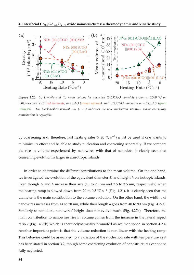
4. Interfacial Ce0:9Gd0:1O2y oxide nanostructures: a thermodynamic and kinetic study
(a)
True
nuc
leat
ion
20 15 10 5 007
1421283542
Mea
n vo
lum
e of
a n
anoi
slan
d (1
02 nm
3 )
Heating Rate (ºC·s-1)
NDs (001)CGO||(001)LAO
NDs (001)CGO||(001)YSZ
NWs (011)CGO||(011)LAO(b)
0
1
2
3
20 15 10 5 0
Den
sity
(103
isla
nds·µm
-2)
Heating Rate (ºC·s-1)
NDs (001)CGO||(001)LAO
NDs (001)CGO||(001)YSZ
NWs (011)CGO||(011)LAOTr
ue n
ucle
atio
n
Figure 4.20: (a) Density and (b) mean volume for quenched (001)CGO nanodots grown at 1000 ºC on
(001)-oriented YSZ (red diamonds) and LAO (orange squares), and (011)CGO nanowires on (011)LAO (green
triangles). The black-dashed vertical line (- - -) indicates the true nucleation situation where coarsening
contribution is negligible.
by coarsening and, therefore, fast heating rates (〈20 ºCs1) must be used if one wants to
minimize its effect and be able to study nucleation and coarsening separately. If we compare
the rise in volume experienced by nanowires with that of nanodots, it clearly seen that
coarsening evolution is larger in anisotropic islands.
In order to determine the different contributions to the mean volume. On the one hand,
we investigated the evolution of the equivalent diameter D and height h on isotropic islands.
Even though D and h increase their size (10 to 20 nm and 2.5 to 3.5 nm, respectively) when
the heating ramp is slowed down from 20 to 0.5 ºCs1 (Fig. 4.21), it is clearly seen that the
diameter is the main contribution to the volume evolution. On the other hand, the width a of
nanowires increases from 14 to 20 nm, while their length b goes from 40 to 90 nm (Fig. 4.22a).
Similarly to nanodots, nanowires’ height does not evolve much (Fig. 4.22b). Therefore, the
main contribution to nanowires rise in volume comes from the increase in the lateral aspect
ratio c (Fig. 4.22b) which is thermodynamically promoted as we mentioned in section 4.2.4.
Another important point is that the volume reduction is non-linear with the heating ramp.
This behavior could be associated to a variation of the nucleation rate with temperature as it
has been stated in section 3.2, though some coarsening evolution of nanostructures cannot be
fully neglected.
84

4.3. Nucleation of CGO nanoislands
4.3.3 Influence of temperature on nucleation
To prove that nucleation rates depend on temperature, we performed various experiments
from 800 to 1200 ºC, at 20 ºCs1 with a fast cooling down to temperatures below 600 ºC at
〈20-40 ºCs1. Fig. 4.23 presents the increase of island dimensions with temperature for
(001)CGO nanodots on (001)YSZ and (001)LAO substrates, and (011)CGO nanowires on
(011)LAO substrates. If we compare Figs. 4.23a and b, we can see that CGO nanodots on YSZ
nucleate at higher temperatures than those grown on LAO. The possible thermodynamic and
kinetic reasons for this phenomenon will be explained later.
Another point to highlight is the fast evolution of these heterostructures at temperatures
as low as 800 ºC. Although it may seem by AFM that the system consists of a continuous and
granular film (Fig. 4.23b), HAADF-STEM analysis reveals that it is instead arranged in the form
of isolated and relaxed epitaxial islands only in 50 seconds from room temperature to 800 ºC,
as indicated in Fig. 4.24 for (001)CGO nanodots on (001)LAO.
More importantly, temperature indeed has an influence over nucleation rates. This is more
clearly seen in Fig. 4.25, where a significant decrease in density is achieved by rising the
annealing temperature. If we fit the data considering the barrier term of the nucleation rate
(Eq. 3.15) and G having the form described in Eq. 4.5a with ν=(vLmT ) =Tmp, we can
obtain the initial density of nuclei N0 and the latent heat of melting per unit volume Lm for
each type of nanoisland. Parameters used for the calculations are h=1:1 nm, v=0:158 nm3,
Tmp=2400 ºC; and values for each heterostructure can be found in Table 4.3 and have been
(a) (b)
20 15 10 5 0
5
10
15
20
25
D (nm
)
Heating Rate (ºC·s-1)
NDs (001)CGO||(001)LAO
NDs (001)CGO||(001)YSZ NDs (001)CGO||(001)LAO
NDs (001)CGO||(001)YSZ20 15 10 5 02.0
2.5
3.0
3.5
4.0
h (n
m)
Heating Rate (ºC·s-1)
Figure 4.21: Dependence with the heating rate of: (a) the equivalent diameter D, and (b) the height, for (001)CGO
nanodots on (001)-oriented YSZ (red diamonds) and LAO (orange squares) substrates. Samples were grown at
1000 ºC without dwell time.
85

4. Interfacial Ce0:9Gd0:1O2y oxide nanostructures: a thermodynamic and kinetic study
1.0
1.5
2.0
2.5
3.0
c=(b
/a)1
/2
1.2
1.6
2.0
2.4
2.8
Height (nm
)
20 15 10 5 0Heating Rate (ºC·s-1)
(a) (b)
20 15 10 5 012
14
16
18
20
22
Wid
th (nm
)
Heating Rate (ºC·s-1)20
40
60
80
100
Length (nm
)Figure 4.22: Heating ramp dependence of nanowires (a) width a (red circles) and length b (blue squares), and (b)
lateral aspect ratio c (green triangles) and height h (orange hexagons). Samples were grown at 1000 ºC doing a
quench.
calculated using the expressions and constants reported in section 4.1.
Table 4.3 shows that despite (001)CGO nanodots on (001)LAO have a similar value of Lm
to (001)CGO on (001)YSZ, i. e. 4.8109 Jm3 and 5.0109 Jm3 respectively, N0 is two orders
of magnitude larger. This could point out towards an enhanced driving force for nucleation
at 0 K for nanodots on LAO compared to those grown on YSZ. On the other hand, (011)CGO
nanowires on (011)LAO present a Lm around three times lower than nanodots, while N0 is
between three and five orders of magnitude larger. Despite it may seem that a small variation of
the experimental values may lead to a large change in the results obtained, it should be noticed
that the derived parameters must have a physical meaning. For instance, the nucleation barrier
G must be positive and increase with temperature, which will highly depend on the value
of Lm. In the case of nanowires, data fitting has been done assuming that the initial nuclei have
a lateral aspect ratio 1.8<c<2.5; otherwise, either fitting was impossible or G was negative.
Table 4.3: and values for the different heterostructures studied. This parameters have been calculated using
the expressions and constants reported in section 4.1. Initial density of nanoislands (N0) and the latent heat of
melting per unit volume (Lm) obtained from data fitting.
Heterostructure Γ (J·m2) Ψ (J·m2) N0 (islands · µm2) Lm (109 J·m3)
(001)CGOk(001)YSZ 0.47 1.50 2:7 104 5.0
(001)CGOk(001)LAO 0.71 1.67 4:2 106 4.8
(011)CGOk(011)LAO 0.63 0.52 5 1010 1.6
86
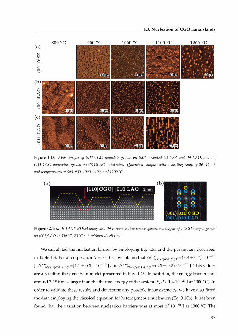
4.3. Nucleation of CGO nanoislands
(a)800 ºC
(001
)YSZ
(001
)LA
O900 ºC 1000 ºC 1100 ºC
(b)
1200 ºC
0.1 µm 0.1 µm
0.1 µm 0.1 µm
0.1 µm 0.1 µm
(c)
0.1 µm0.1 µm 0.1 µm(011
)LA
O
0.1 µm
0.1 µm 0.1 µm
Figure 4.23: AFM images of (011)CGO nanodots grown on (001)-oriented (a) YSZ and (b) LAO, and (c)
(011)CGO nanowires grown on (011)LAO substrates. Quenched samples with a heating ramp of 20 ºCs1
and temperatures of 800, 900, 1000, 1100, and 1200 ºC.
(b)(a)
(001)[011]CGO(001)[010]LAO
[110]CGO||[010]LAO
Figure 4.24: (a) HAADF-STEM image and (b) corresponding power spectrum analysis of a CGO sample grown
on (001)LAO at 800 ºC, 20 ºCs1 without dwell time.
We calculated the nucleation barrier by employing Eq. 4.5a and the parameters described
in Table 4.3. For a temperature T=1000 ºC, we obtain that GNDs=(001)Y SZ=(3:8 0:7) 1020
J, GNDs=(001)LAO=(1:1 0:5) 1019 J and GNWs=(011)LAO=(2:5 0:8) 1019 J. This values
are a result of the density of nuclei presented in Fig. 4.25. In addition, the energy barriers are
around 3-18 times larger than the thermal energy of the system (kBT〈1.41020 J at 1000 ºC). In
order to validate these results and determine any possible inconsistencies, we have also fitted
the data employing the classical equation for heterogeneous nucleation (Eq. 3.10b). It has been
found that the variation between nucleation barriers was at most of 1020 J at 1000 ºC. The
87

4. Interfacial Ce0:9Gd0:1O2y oxide nanostructures: a thermodynamic and kinetic study
NDs (001)CGO||(001)LAO
NDs (001)CGO||(001)YSZ
NWs (011)CGO||(011)LAO
0.0
0.6
1.2
1.8
2.4
3.0
900 1000 1100 1200
Den
sity
(103 i
sland
s·µm
-2)
Temperature (ºC)
Figure 4.25: Density of nanostructures as a function of temperature for CGO nanodots on (001)-YSZ (red
diamonds) and LAO (orange squares), and (011)CGO nanowires on (011)LAO (green triangles). Solid lines
indicate the fitting of the nucleation rate for each heterostructure from Eqs. 3.15 and 4.5a. Parameters used for the
calculations are h=1:1 nm, v=0:158 nm3, and appropiate parameters from Table 4.1.
nucleation barrier of CGO nanodots on YSZ is around one order of magnitude smaller than
that on LAO which does not explain why no islands can be appreciated below 1000 ºC for CGO
on YSZ. A more theoretical approach to the thermodynamic origin of the shift in nucleation
will be discussed in section 4.3.4.
Regardless of the results presented, it cannot be completely discarded the influence of
coarsening since at these high temperatures atomic diffusion is very important. In fact, a
theoretical work from Meixner et al. [149] pointed out that kinetic mechanisms rule over
thermodynamics in nucleation, leading to a temperature-enhanced enlargement of sizes. Fig.
4.26 present the variation of volume with the heating rate at 1000 ºC plotted together with the
temperature variation at 20 ºCs1 for CGO nanodots and nanowires. The kinetic evolution of
isotropic nanoislands at 20 ºCs1 rises with temperature indicating that some coarsening may
be present, although it is smaller than the one achieved using slow heating ramps (Figs. 4.26a
and b). The only case where the evolution with temperature seems to compete with that of the
heating rate is for CGO nanodots on YSZ annealed above 1100 ºC (Fig. 4.26a). The trend
followed by nanowires (Fig. 4.26c) is the same as the one observed for nanodots, although
temperature evolution seems more important, especially for temperatures above 1000 ºC
where the mean volume of nanowires is of the same order of that at the slowest heating rates.
The isothermal coarsening evolution of nanoislands will be investigated in section 4.4.
88

4.3. Nucleation of CGO nanoislands
4.3.4 Thermodynamic analysis of the shift in nucleation between islands grown on
(001)YSZ and (001)LAO
In the previous section we have shown that nucleation rates decrease with temperature (Fig.
4.23). Then, it seems logic to analyze what parameters influence those barriers (section 3.2.1).
The first thing to stress out is what it seems to be a shift to higher temperatures of nucleation
for CGO nanodots on (001)YSZ as compared to (001)LAO. This phenomenon could not be
attributed to a higher nucleation barrier for CGO on (001)YSZ since we have demonstrated that
it is actually one order of magnitude smaller. However, the calculation of nucleation barriers
has been done without considering the influence of strain and interface energies.
The contribution of strain is easily addressed as shown in sections 3.2.2 and 4.2.5. In
essence, nanodots grown on YSZ have a larger strain configuration than those grown on LAO
("CGOjjY SZ〈5% vs "CGOjjLAO〈1%). Large values of strain will rise the energy barrier for a
given supersaturation and delay nucleation [126, 128]. Hence, more energy will be needed in
the system to overcome the energy barrier and achieve nucleation, i. e. higher temperatures
will supply more thermal energy.
Usually, nucleation barriers are determined assuming only island surface energies (Eq.
4.5a). However, the interface energy may also contribute shifting the barrier to different
values of supersaturation. Since CGO and YSZ have a fluorite structure, we assumed that its
interface energy must be lower than that on LAO (perovskite structure) for the representation
of the nucleation barriers. Thus, we used CGOY SZi =0.5 Jm2 and CGOLAOi =1 Jm2 for
the calculations. Fig. 4.27 shows that the nucleation barrier of CGO on YSZ is shifted to low
20 15 10 5 00
3
6
9
12
15
1200 ºC
Mea
n vo
lum
e (1
02 n
m3 )
Heating Rate (ºC·s-1)
1100 ºC
1000 ºC
(a) (b) (c)
20 15 10 5 0
Heating Rate (ºC·s-1)
0
10
20
30
40
Mea
n vo
lum
e (1
02 n
m3 )
900 ºC
1100 ºC
1000 ºC
(001)CGO on (001)YSZ (001)CGO on (001)LAO
20 15 10 5 00
3
6
9
12
15
Mea
n vo
lum
e (1
02 n
m3 )
Heating Rate (ºC·s-1)
1100 ºC 1000 ºC
800 ºC 900 ºC
(011)CGO on (011)LAO
Figure 4.26: Mean volume dependence on temperature for (001)CGO nanodots on (a) (001)YSZ (diamonds), (b)
(001)LAO (squares), and (c) (011)CGO nanowires on (011)LAO (triangles). The heating rate dependence at 1000
ºC has been plotted for comparison.
89

4. Interfacial Ce0.9Gd0.1O2−y oxide nanostructures: a thermodynamic and kinetic study
2.0 2.5 3.0 3.5 4.0 4.5 5.00
200
400
600
800
1000
G* (
10-1
9 J)
∆µ (10-19 J)
CGO on(001)YSZ
CGO on (001)LAO
T∆µ,∆T
Figure 4.27: Nucleation barriers for CGO on (001)-oriented YSZ (—) and LAO (—) substrates. The dashed
arrows indicate the displacement caused by an increase in the interface energy. Values of interface energies are
γCGO−Y SZi =0.5 J· m−2 and γCGO−LAOi =1 J· m−2.
values of supersaturation (∆ µ ∼∆T=Tm−T ) which goes in favor of the fact that the nucleation
temperature must be higher than for CGO on LAO. If we consider the influence of interface
energy (γY SZi =0.5 J· m−2 and γLAOi =1 J· m−2), it can be seen that Eint moves the barriers to large
values of ∆ µ and given that the interface energy of CGO on LAO should be much larger, its
energy barrier must be shifted to even higher supersaturations. Therefore, a higher
supersaturation (lower temperature) is needed to nucleate CGO nanodots on LAO.
4.3.5 Transformation of CGO isotropic to anisotropic islands on (001)LAO
substrates
The growth of (011)CGO nanowires can be also achieved on (001)LAO if the annealing
atmosphere is changed to Ar-H2 [52]. In this case, the study of the influence of the heating
ramp reveals an interesting transition between isotropic and anisotropic nanostructures (Fig.
4.28a). Coexistent self-assembled islands presenting different crystallographic orientations is a
phenomenon that appears to be rather natural in many oxides [53, 173] and could be related to
nucleation events with close energy barriers.
The detailed analysis of islands’ density (Fig. 4.28b) shows that at fast heating rates the
system consists mainly of orthogonal nanowires, while the presence of nanodots rises when
the heating ramp is slowed down. A plausible explanation is that by using fast rates the
system goes directly to temperatures where nucleation of nanowires is promoted over
90

4.3. Nucleation of CGO nanoislands
nanodots, whilst using slow heating ramps it goes first through the nanodots nucleation
barrier. Indeed, similar experiments varying temperature as the ones performed by Gibert et
al. [51] but at faster heating rates (20 ºCs1) show a transition between (001) nanodots and
(011) nanowires with temperature (Fig. 4.29a), which is related to a lower energy barrier for
the (001) orientation at large values of ν, i. e. low temperatures, as we see from
thermodynamic calculations (Fig. 4.29b).
0.1 µm0.1 µm
0.1 µm0.1 µm
20 ºC·s-1 10 ºC·s-1
5 ºC·s-1 0.5 ºC·s-1
(a) (b)
20 15 10 5 00
100
200
300
400 Nanodots Nanowires
Den
sity
(isla
nds·µ
m-2)
Heating rate (ºC·s-1)
Figure 4.28: (a) AFM images and (b) density illustrating the transformation from (001)CGO nanodots (red
pentagons) and (011)CGO nanowires (orange squares) grown on (001)-oriented LAO substrates at 1000 ºC, in
Ar-H2 atmosphere with no dwell time. Heating rates investigated are: 20, 10, 5, and 0.5 ºCs1.
0.1 µm
0.25 µm0.1 µm
800 ºC
1000 ºC 1100 ºC
(a) (b)
0.1 µm
900 ºC
2 3 4 50
200
400
600
G*
(10-1
9 J)
∆µ (10-19 J)
(011)CGOorientation
(001)CGOorientation
Figure 4.29: (a) AFM images of (001)CGO nanodots and (011)CGO nanowires on (001)LAO and temperatures
of 800, 900, 1000 and 1100 ºC, at 20 ºCs1. (b) Nucleation barrier for the formation of both (001) (—) and (011)
(—) CGO nanostructures as a function of the chemical potential (ν) (Reproduced from [51]).
91
4. Interfacial Ce0:9Gd0:1O2y oxide nanostructures: a thermodynamic and kinetic study
4.4 Coarsening of CGO nanoislands
Besides the thermodynamic aspects leading to nucleation of islands as a relaxation mechanism
in highly strained systems, the influence of diffusion mechanisms also plays an important role
in the definition of island’s size and shape [182]. In CSD-derived systems, all the material
have already been deposited from the beginning of nanoislands formation and growth. Thus,
we expect our system to likely behave close to a thermodynamic equilibrium, contrarily to
what is observed in physical methods such as pulsed laser deposition. Nevertheless, a great
discussion has been generated in relation to whether thermodynamic or kinetic mechanisms
control nanostructuration.
After successfully identifying the conditions that allowed us to reduce the effect of
coarsening with the heating ramp and study nucleation separately (section 4.3.2), we can
evaluate the true contribution of coarsening for the different nanostructures. AFM analyses of
(001)CGO nanodots on (001)YSZ (Fig. 4.30) and (001)LAO (Fig. 4.31), and (011)CGO
nanowires on (001) and (011)LAO (Fig. 4.32), respectively, show their sizes increase with both
temperature and time.
Actually, we already knew that temperature had an effect on the volume of nanoislands
(Fig. 4.26), which was mainly attributed to nucleation events, although coarsening could
contribute too. A more careful analysis of the mean volume dependence with time reveals
that its rise is similar for both isotropic nanodots on (001)YSZ and (001)LAO (Figs. 4.33a and
b), while nanowires are greatly affected by coarsening (Fig. 4.33c). This proves what has
already been reported from thermodynamic calculations in the literature [139, 166] and
anticipated in section 4.2.4 for our particular systems. Coarsening of nanodots is
thermodynamically promoted until they reach an optimum equilibrium size Dopt (Fig. 4.8c),
whereas nanowires continuously enlarge to reduce the energy of the system (Fig. 4.10).
Regarding the particular case of nanoislands obtained in Ar-H2, we can see that nanodots
follow a similar trend as the ones grown in O2 (Fig. 4.33b); despite they should have an
increased kinetic evolution provided they are grown in a reducing atmosphere. On the other
hand, orthogonal nanowires present a relatively faster evolution than those obtained in O2.
This could be attributed to the particularly large amount of oxygen vacancies introduced by
their structural arrangement on LAO substrates, as well as the Ar-H2 annealing atmosphere
(section 4.2.3) together with thermodynamic and kinetic mechanisms that will be discussed in
section 4.4.2.
92

4.4. Coarsening of CGO nanoislands
0.1 µm
0.1 µm
0 min
900
ºC10
00 º
C
5 min 15 min 30 min
0.1 µm 0.1 µm 0.1 µm
0.1 µm0.1 µm
Figure 4.30: AFM images showing the coarsening evolution at different temperatures of (001)CGO nanodots
grown on (001)YSZ substrates in O2. The heating ramp is 20 ºCs1.
0.1 µm0.1 µm0.1 µm
0 min
900
ºC10
00 º
C
5 min 15 min 30 min
1100
ºC
0.1 µm
0.1 µm
0.1 µm
0.1 µm
0.1 µm
0.1 µm
0.1 µm
800
ºC
O2
Ar-H2
0.1 µm
(a)
(b)
0.1 µm
0.1 µm
Figure 4.31: AFM images of the kinetic evolution with time, using a heating rate of 20 ºCs1 for (001)CGO
nanodots grown on (001)LAO substrates at (a) 800 ºC in Ar-H2, and (b) 900, 1000 and 1100 ºC in O2.
93
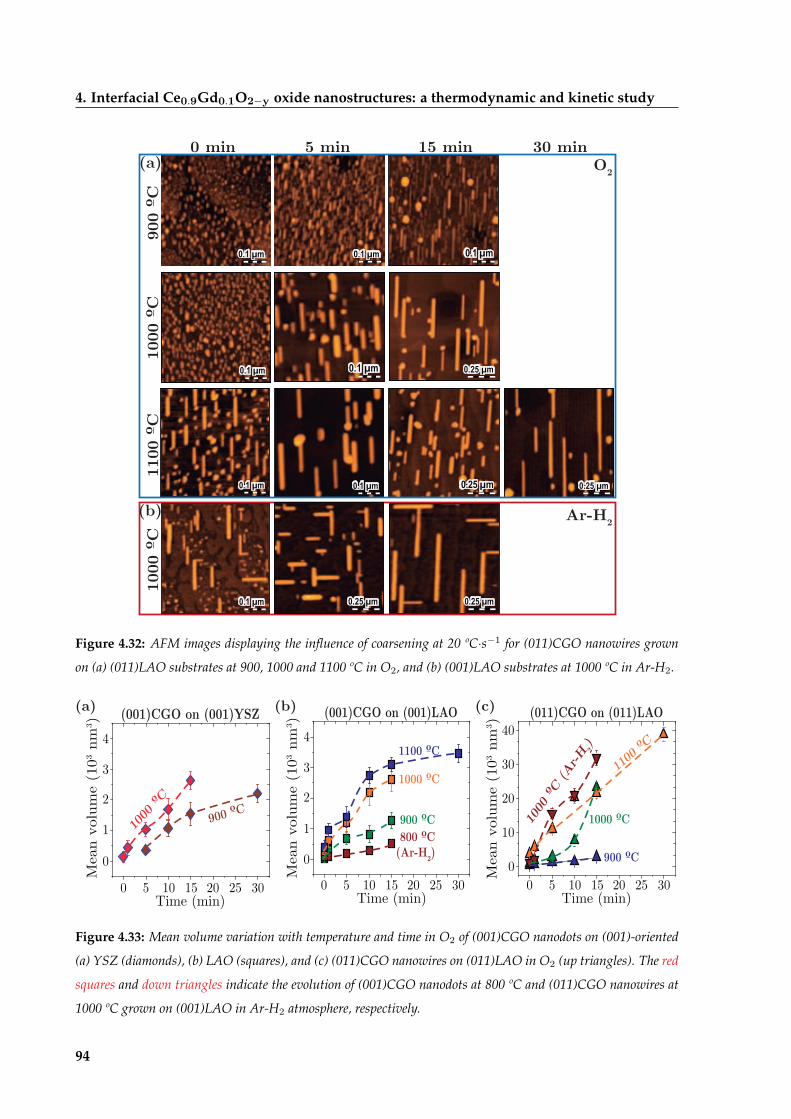
4. Interfacial Ce0:9Gd0:1O2y oxide nanostructures: a thermodynamic and kinetic study
0.25 µm0.1 µm
0 min90
0 ºC
1000
ºC
5 min 15 min 30 min11
00 º
C
0.1 µm 0.1 µm 0.1 µm
0.1 µm 0.1 µm
0.1 µm 0.1 µm 0.25 µm
0.25 µm
0.25 µm
O2
Ar-H2
1000
ºC
0.25 µm
(a)
(b)
Figure 4.32: AFM images displaying the influence of coarsening at 20 ºCs1 for (011)CGO nanowires grown
on (a) (011)LAO substrates at 900, 1000 and 1100 ºC in O2, and (b) (001)LAO substrates at 1000 ºC in Ar-H2.
(a) (b)
0
1
2
3
4
0 5 10 15 20 25 30Time (min)
900 ºC
1000
ºC
(001)CGO on (001)YSZ
Mea
n vo
lum
e (1
03 n
m3 )
Mea
n vo
lum
e (1
03 n
m3 )
0
1
2
3
4
(001)CGO on (001)LAO
1100 ºC
1000 ºC
900 ºC 800 ºC(Ar-H2)
0 5 10 15 20 25 30Time (min)
0 5 10 15 20 25 30Time (min)
900 ºC
1100
ºC
1000 ºC
1000 ºC
(Ar-H
2)
Mea
n vo
lum
e (1
03 n
m3 )
0
10
20
30
40(011)CGO on (011)LAO(c)
Figure 4.33: Mean volume variation with temperature and time in O2 of (001)CGO nanodots on (001)-oriented
(a) YSZ (diamonds), (b) LAO (squares), and (c) (011)CGO nanowires on (011)LAO in O2 (up triangles). The red
squares and down triangles indicate the evolution of (001)CGO nanodots at 800 ºC and (011)CGO nanowires at
1000 ºC grown on (001)LAO in Ar-H2 atmosphere, respectively.
94

4.4. Coarsening of CGO nanoislands
(a) (b)
(001
)CG
O on
(001
)YSZ
Dia
mte
r, D
(nm
)
5
10
15
20
25
0 5 10 15 20 25 30Time (min)
900 ºC
1000 ºC
Hei
ght, h
(nm
)
2
3
4
5
6
0 5 10 15 20 25 30Time (min)
7
900 ºC
1000 ºC
(c) (d)
(001
)CG
O on
(001
)LAO
Dia
mte
r, D
(nm
)
51015
2025
0 5 10 15 20 25 30Time (min)
0
30
1100 ºC 1000 ºC 900 ºC 800 ºC(Ar-H2)
Hei
ght, h
(nm
)
23456
0 5 10 15 20 25 30Time (min)
7
1
8 1100 ºC
1000 ºC
900 ºC
800 ºC(Ar-H2)
Figure 4.34: Dependence with temperature and time of: (a) the equivalent diameter and (b) height for (001)CGO
nanodots on (001)YSZ in O2 (diamonds), and (c) the equivalent diameter and (d) height for (001)CGO nanodots
on (001)LAO in O2 (squares). The red squares indicate the evolution of (001)CGO nanodots grown on (001)LAO
at 800 ºC in Ar-H2 atmosphere.
4.4.1 Coarsening of CGO nanodots driven by atomic mobility
The separate investigation between the different contributions to nanodots volume (Figs. 4.33a
and b), i. e. the equivalent diameter and height should allow us to identify which one has a
main influence on their coarsening.
Fig. 4.34 presents the diameter and height evolution for isotropic nanodots with
temperature and time. A similar trend to the one observed for the volume (Figs. 4.33a and b)
can be identified, i. e. both dimensions increase with temperature and time, showing a
saturation behavior which is more pronounced at high temperature.
If we fit the data considering a self-limited growth (Eq. 3.22), we can obtain the relaxation
times for in-plane θNDsk and out-of-plane θNDs? directions (Figs. 4.35a and b). Both relaxation
times decrease with temperature which could indicate an enhanced atomic mobility at higher
95

4. Interfacial Ce0:9Gd0:1O2y oxide nanostructures: a thermodynamic and kinetic study
temperatures. Furthermore, θNDsk shrinks faster than θNDs? , and thus, diffusion should be faster
along the in-plane direction.
The in-plane and out-of-plane diffusion coefficients (DNDsk and DNDs
? ) can be extracted
from islands’ dimensions and relaxation times by applying Eq. 3.23 (Figs. 4.35c and d). Both
diffusion coefficients rise with temperature and DNDsk is around one order of magnitude larger
(a) (b)
012345678
800 900 1000 1100Temperature (ºC)
In-p
lane
diff
. coe
ff.,
D||
(10
-19 m
2 ·s-1)
ND
s (001)CGOon (001)LAO
(001)CGOon (001)YSZ
0
0.3
0.6
0.9
800 900 1000 1100Temperature (ºC)
In-p
lane
rela
x. ti
me,
τ || (1
03 s)
ND
s
(001)CGO on (001)LAO
(001)CGOon (001)YSZ
(c) (d)
0.0
0.1
0.2
0.3
800 900 1000 1100Temperature (ºC)
Out
-of-p
lane
diff
.co
eff.,
D⊥
(10-1
9 m2 ·s
-1)
ND
s
(001)CGOon (001)LAO
(001)CGOon (001)YSZ
(e) (f)
-47.0
-46.5
-46.0
-45.5
-45.0
Log
of
D⊥N
Ds
7.0 8.0 8.5 9.0 9.5104/T (K-1)
7.5
Qd,⊥ =(1.1±0.2)·10-19 JD0,⊥ =(9.8±0.1)·10-18 m2·s-1
(001)CGOon (001)LAO
(001)CGO on (001)YSZ
NDs
NDs
0.4
0.5
0.6
0.7
800 900 1000 1100Temperature (ºC)
Out
-of-p
lane
rela
x.tim
e, τ ⊥
(1
03 s)
ND
s
(001)CGO on (001)LAO
(001)CGOon (001)YSZ
-44.0
-43.5
-43.0
-42.5
-42.0
Log
of
D||
7.0 8.0 8.5 9.0 9.5104/T (K-1)
ND
s
7.5
Qd,|| =(1.3±0.2)·10-19 JD0,|| =(6.0±0.1)·10-16 m2·s-1NDs
NDs
(001)CGOon (001)LAO
(001)CGOon (001)YSZ
Figure 4.35: Dependence with temperature of: (a) in-plane and (b) out-of-plane relaxation times (θNDsk and
θNDs? ), and (c) in-plane and (d) out-of-plane diffusion coefficients (DNDsk and DNDs
? ). Arrhenius plots of (e)
DNDsk and (f)DNDs
? . (001)CGO nanodots on (001)YSZ and (001)LAO are represented by diamonds and squares,
respectively.
96

4.4. Coarsening of CGO nanoislands
than DNDs? , as predicted from the temperature dependence of the relaxation times.
Since diffusion seems to follow an Arrhenius-like thermally-activated process (Eq. 3.24), the
corresponding Arrhenius plots allow a more detailed analysis of this process from the in-plane
and out-of-plane activation energies (QNDsd;k and QNDsd;? ) and pre-exponential factors (DNDs0;k and
DNDs0;? ). On the one hand, the activation energy QNDsd;k =(1:3 0:2)1019 J is marginally higher
than QNDsd;? =(1:1 0:2)1019 J, therefore, a little more energy is required to activate in-plane
diffusion. Despite it should be noted that both activation energies are around 6-7 times larger
than kBT (= 1:761020 J at 1273 K), this values are in agreement with those reported in systems
with thermally-activated coarsening [159, 161, 183].
On the other hand, DNDs0;k =(6:0 0:1)1016 m2s1 is 60 times larger than DNDs
0;? =(9:8
0:1)1018 m2s1. Essentially, this could be understood as the driving force for in-plane atomic
mobility being substantially larger than the out-of-plane one.
4.4.2 Diffusion-enhanced enlargement of CGO nanowires
Likewise, the different contributions to nanowires’ volume (Fig. 4.33c) can be evaluated
separately as shown in Fig. 4.36. An equivalent saturation behavior to that observed for
nanodots in section 4.4.1 can be seen for nanowires’ width and height, whereas their length
seems to saturate at significantly longer times.
(a) (b) (c)
Wid
th, a
(nm
)
12
16
20
24
0 5 10 15 20 25 30Time (min)
900 ºC 1000 ºC
1100 ºC
1000 ºC(Ar-H2)
Len
gth,
b (
nm)
50
100
150
200
250
0 5 10 15 20 25 30Time (min)
0
300
900 ºC
1100 ºC
1000 ºC(Ar-H2)
1000 ºC
Hei
ght, h
(nm
)
0
2
4
6
0 5 10 15 20 25 30Time (min)
8
900 ºC
1100 ºC
1000 ºC(Ar-H2)
1000 ºC
Figure 4.36: Dependence with temperature and time of: (a) the width a, (b) length b and (c) height h for (011)CGO
nanowires on (011)LAO in O2 (up triangles). The red down triangles indicate the evolution of (011)CGO
nanowires grown on (001)LAO at 1000 ºC in Ar-H2 atmosphere.
Fitting the data applying the previously mentioned self-limiting model (Eq. 3.22) allow
us to extract the relaxation times for nanowires’ width θNWsk;a , length θNWs
k;b and height θNWs?
(Figs. 4.37a-c). On the one hand, we confirm that θNWsk;a and θNWs
? decrease with temperature
following an equivalent trend to that of nanodots (Figs. 4.35a and b). On the other hand, θNWsk;b
97
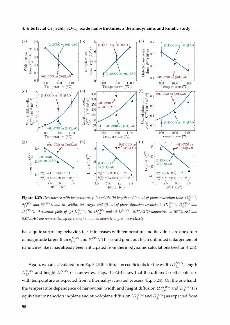
4. Interfacial Ce0:9Gd0:1O2y oxide nanostructures: a thermodynamic and kinetic study
(a) (b) (c)
900 1000 1100Temperature (ºC)
Wid
th r
elax.
tim
e, τ ||,a
(1
03 s)
NW
s
0.1
0.2
0.3
0.4
0.5
0.6(011)CGO on (011)LAO
(011)CGO on (001)LAO
(d) (e) (f)
900 1000 1100Temperature (ºC)
0.4
0.5
0.6
0.7
Out
-of-p
lane
rela
x.
time,
τ ⊥
(103 s
)N
Ws
(011)CGO on (011)LAO
(011)CGO on (001)LAO
900 1000 1100Temperature (ºC)
Leng
th r
elax
. t
ime,
τ||,b
(10
3 s)
NW
s
2
8
6
4
0
(011)CGO on (011)LAO
(011)CGO on (001)LAO
012345678
Wid
th d
iff. c
oeff.
,D
||,a
(10
-19 m
2 ·s-1)
NW
s
900 1000 1100Temperature (ºC)
(011)CGO on (011)LAO
(011)CGO on (001)LAO
050
100150200250300350
Leng
th d
iff. c
oeff.
,D
||,b
(10
-19 m
2 ·s-1)
NW
s
900 1000 1100Temperature (ºC)
(011)CGO on (011)LAO
(011)CGO on (001)LAO
Out
-of-p
lane
diff
.co
eff.,
D⊥
(10-1
9 m2 ·s
-1)
NW
s
0.0
0.1
0.2
0.3
900 1000 1100Temperature (ºC)
(011)CGO on (011)LAO
(011)CGO on (001)LAO
Qd,||,b =(2.2±0.9)·10-19 JD0,||,b =(5.2±0.6)·10-12 m2·s-1
NWs
NWs
(g) (h) (i)
-47
-46
-45
Log
of
D||,bNW
s
7.0 8.0 8.5104/T (K-1)
7.5
-44
-43
-42
Log
of
D||,aNW
s
7.0 8.0 8.5104/T (K-1)
7.5
Qd,||,a =(1.7±0.6)·10-19 JD0,||,a =(3.6±0.2)·10-15 m2·s-1
NWs
NWs
(011)CGOon (011)LAO
(011)CGO on (001)LAO
(011)CGOon (011)LAO
(011)CGO on(001)LAO
NWs
NWs
Qd,⊥ =(2.6±0.9)·10-19 JD0,⊥ =(3.4±0.5)·10-14 m2·s-1
-47
-46
-45
7.0 8.0 8.5104/T (K-1)
7.5
-48
Log
of
D⊥N
Ws
(011)CGOon (011)LAO
(011)CGO on(001)LAO
Figure 4.37: Dependence with temperature of: (a) width, (b) length and (c) out-of-plane relaxation times (θNWsk,a ,
θNWsk,b and θNWs
? ), and (d) width, (e) length and (f) out-of-plane diffusion coefficients (DNWsk,a , DNWs
k,b and
DNWs? ). Arrhenius plots of (g) DNWs
k,a , (h) DNWsk,b and (i) DNWs
? . (011)CGO nanowires on (011)LAO and
(001)LAO are represented by up triangles and red down triangles, respectively.
has a quite surprising behavior, i. e. it increases with temperature and its values are one order
of magnitude larger than θNWsk;a and θNWs
? . This could point out to an unlimited enlargement of
nanowires like it has already been anticipated from thermodynamic calculations (section 4.2.4).
Again, we can calculated from Eq. 3.23 the diffusion coefficients for the widthDNWsk;a , length
DNWsk;b and height DNWs
? of nanowires. Figs. 4.37d-f show that the different coefficients rise
with temperature as expected from a thermally-activated process (Eq. 3.24). On the one hand,
the temperature dependence of nanowires’ width and height diffusion (DNWsk;a and DNWs
? ) is
equivalent to nanodots in-plane and out-of-plane diffusion (DNDsk andDNDs
? ) as expected from
98

4.4. Coarsening of CGO nanoislands
their corresponding relaxation times, i. e. DNWsk;a is around one order of magnitude larger than
DNWs? . On the other hand, DNWs
k;b is around two and three orders of magnitude larger than
DNWsk;a and DNWs
? , respectively, which again evidences an enhanced coarsening of nanowires’
length.
Like nanodots, the Arrhenius plots of DNWsk;a , DNWs
k;b and DNWs? (Figs. 4.37g-i) allow a more
exhaustive analysis of the diffusion process from the calculation of the activation energies
(QNWsd;k;a , QNWs
d;k;b and QNWsd;? ) and pre-exponential factors (DNWs
0;k;a , DNWs0;k;b and DNWs
0;? ). Although,
it can be seen that the activation energy QNWsd;k;a =(1:7 0:6)1019 J is in a similar range to
QNWsd;k;b =(2:2 0:9)1019 J and QNWs
d;? =(2:6 0:9)1019 J, we expect that less thermal energy
should be necessary to activate the width diffusion process compared to the other ones.
Notice that the activation energies are between 9 and 15 times larger than kBT (= 1:761020 J
at 1273 K), again in line with thermally-activated coarsening processes [159, 161, 183]. These
values of QNWsd are around two times higher than the activation energies for nanodots
diffusion which should indicate a delayed diffusion for nanowires to higher temperatures.
If we look at the pre-exponential factors, the driving force for width diffusionDNWs0;k;a =(3:6
0:2)1016 m2s1 is two and four orders of magnitud smaller than DNWs0;? =(3:4 0:5)1014
m2s1 andDNWs0;k;b =(5:20:6)1012 m2s1, respectively. Consequently, the larger length driving
force can compensate the higher activation energies improving coarsening of that direction.
In summary, we have demonstrated that nanowires’ width and height atomic diffusions
behave similarly to nanodots’ diameter and height, i. e. DNDsk and DNWs
k;a have faster atomic
diffusions versus temperature than DNDs? and DNWs
? as shown in Fig. 4.38. Finally, nanowires
could enlarge almost indefinitely because their length diffusion versus temperature is even
faster than DNWsk;a and DNWs
? (Fig. 4.38b).
Several reasons may contribute to the phenomena described. Considering the case of
isotropic islands, there exists a thermodynamic driving force promoting islands’ growth until
they reach an optimum stable size and it decreases as sizes approach to that value (Fig. 4.8c).
In addition, nuclei are close to each other during early stages of growth which also facilitates
diffusion of atoms. Finally, the presence of a repulsive strain field with origin in the isotropic
biaxial strain stimulates nucleation, while it hinders the growth rate as islands grow [184].
Although atomic diffusion also influences early stages of growth in anisotropic
nanostructures, there is no thermodynamic restriction towards unlimited growth as shown in
Fig. 4.10. Li et al. noted that nanostructures presenting an anisotropy in surface energies and
shape should enlarge along the lower surface energy facet in order to decrease the overall
99

4. Interfacial Ce0:9Gd0:1O2y oxide nanostructures: a thermodynamic and kinetic study
(a) (b)
0.0
0.1
0.2
0.3
0.4
0.5N
anod
ots
diff.
coef
f. (1
0-19 m
2 ·s-1)
Temperature (ºC)0 200 400 600 800 10001200
D|| NDs
D⊥ NDs
0.0
0.1
0.2
0.3
0.4
0.5
Temperature (ºC)0 200 400 600 800 10001200
Nan
owire
s di
ff.co
eff.
(10-1
9 m2 ·s
-1)
D⊥ NWs
D||,a
D||,b NWs
NWs
Figure 4.38: Comparison between in-plane and out-of-plane atomic diffusions for CGO (a) nanodots and (b)
nanowires.
island energy [185]. Actually, this is what we observe for (011)CGO nanowires on (001) and
(011)LAO substrates which tend to elongate along the direction presenting f111g facets
having the lowest surface energy (Table 4.1).
Gibert et al. proposed additional mechanisms to explain the fast kinetic evolution of
(011)CGO nanowires grown in (001)LAO substrates in Ar-H2 [52]. On the one hand, they
observed dynamic coalescence, i. e. displacement of islands as a whole entity and integration
into another island. On the other hand, attractive/repulsive elastic interactions also played an
important role, where strain fields with opposed sign have an inclination to attract each other
forming connected perpendicular nanowires such as those observed in Fig. 4.32b, while strain
fields with the same sign will repel each other forming arrays of parallel nanowires Figs. 4.32a
and b.
4.5 Summary and conclusions
In this chapter, we have presented the different stable morphologies that can be obtained by
tuning the relation between biaxial strain and surface energies. Essentially, we have shown that
isotropic CGO nanoislands grow on (001)YSZ and (001)LAO substrates in oxygen, whereas if
the substrate orientation or the annealing atmosphere are changed to (011)LAO and Ar-H2,
respectively, it is possible to induce anisotropic islands. The modification of the annealing
atmosphere can be used to tune the oxygen content of these nanostructures and may influence
their kinetic evolution.
Thermodynamic models have been applied to demonstrate the stability and evolution of
CGO nanostructures; while nanodots present a lateral aspect ratio c=1 and should have a
100

4.5. Summary and conclusions
limited coarsening (energy minimum in E=V curves), nanowires have values of c>1 and
should enlarge indefinitely as their E=V decreases by increasing the lateral aspect ratio.
Different interface energies may slightly modify the results obtained in terms of energy and
size (nanodots), as well as lateral aspect ratio (nanowires).
In addition, it has been shown that two different anisotropic shapes have been obtained, i.
e. parallel with a strain configuration of 1% on (011)LAO ([100]CGOk[0-11]LAO and
[0-11]CGOk[010]LAO) or orthogonal nanowires with two possible strain configurations on
(001)LAO, i. e. [0-11]CGOk[010] with a low compressive mismatch of 1% and
[100]CGOk[100]LAO with a high tensile mismatch of 5%. We demonstrated that the reason we
have parallel nanowires on (011)LAO is because the higher energy barrier of the high strain
configuration forbids their nucleation at the experimental conditions employed.
Nucleation and growth of nanostructures have been investigated too. Surprisingly, the
CGO system is already formed at very low temperatures and it can even be epitaxially grown,
oppositely to what is observed commonly in CSD growth. In addition, we demonstrated that
nucleation and kinetic evolution can be studied independently by diminishing the contribution
of coarsening, rising the heating rate from conventional furnace annealing (<0.5 ºCs1) to RTA
(〈20 ºCs1) values.
The dependence with temperature of nanoislands also showed that there was a small
growth in sizes, although it was not comparable to the evolution observed by slowing down
the heating rate. Moreover, it was proved that at relatively low temperatures (〈 800 ºC), there
are already individual epitaxial nanostructures.
Parameters such as strain and interface energy modify nucleation barriers to higher
temperatures as it has been shown experimentally for (001)CGO nanodots on (001)YSZ in
comparison with those grown on (001)LAO. Another example illustrating barriers with
different temperatures was that of CGO on (001)LAO in Ar-H2, where nanodots were able to
grow at slow heating rates, whereas at high rates we were able to select more precisely the
nucleation conditions to form nanowire templates. This effect was related to the dependence
of the nucleation barrier with temperature, i. e. nanodots nucleated at lower temperatures
than nanowires.
Finally, coarsening evolution of nanodots demonstrated that they follow a self-limited
growth process. In addition, atomic diffusion is thermally-activated, i. e. diffusion is
enhanced with temperature, and it is faster in the in-plane direction due to a larger driving
force. Nanowires’ coarsening along their width and height follow a trend similar to nanodots,
101

4. Interfacial Ce0:9Gd0:1O2y oxide nanostructures: a thermodynamic and kinetic study
whereas their length has a larger driving force which could point towards an almost
unlimited evolution in agreement with thermodynamic calculations.
Overall, the deep study undertaken has enabled a better comprehension of the CSD-derived
CGO heteroepitaxial nanoislands, bringing more knowledge on the still poorly understood
nucleation and growth processes of oxide nanostructures. The methodologies and analyses
employed in this chapter could prove fundamental for the investigation and improvement of
nucleation and growth processes of many oxide heterostructures and have been systematically
applied in the next chapters of this thesis.
102

Chapter 5
Functional oxide thin-films grown by
rapid thermal annealing of
metal-organic precursors
Chemical solution deposition (CSD) of metal-organic precursors is a very versatile, scalable
and low cost methodology to obtain oxide thin-films. Few works have been devoted to the
study of nucleation and growth mechanisms and, in most cases, they were focused on the self-
assembling of nanoislands using conventional thermal annealing (CTA) treatments [11, 35, 49–
53] or on the formation of polycrystalline oxide films [186, 187]. It has been demonstrated in
Chapter 4 that nucleation and coarsening of CGO nanoislands can be studied independently
when fast heating are used by means of RTA furnaces. Nonetheless, nucleation is still poorly
understood, particularly for CSD heteroepitaxial thin film growth.
CSD has also been broadly explored to develop crystalline oxide thin-films for optic,
catalytic, electric, magnetic or superconducting applications [21, 32, 40, 45]. To ensure good
physical properties heteroepitaxial growth is often required; typically, involving single
crystalline substrates, high temperatures and long annealing times. Furthermore, grain size
and crystallinity affect those properties in great measure [24, 188]. Therefore, giving more
insight on the crystallization characteristics and microstructural engineering is fundamental to
develop effective ways for thin film growth with high performance functionalities.
Regardless of their scientific and industrial importance, common investigations of CSD film
growth have been only investigated deeply in counted cases such as lead zirconate titanate [152,
189] or more recent publications about cerium oxide [159, 161]. Also, it is notable the case of
103

5. Functional oxide thin-films grown by rapid thermal annealing of metal-organicprecursors
yttrium barium copper oxide (YBCO) where a remarkable effort has been made to understand
nucleation and growth processes in order to produce high-temperature superconducting films
with outstanding properties [21, 190]. Additionally, thin film studies are mainly focused on the
dependence of surface morphology and stress relaxation with thickness or temperature [191,
192], and the small amount of literature that tried to carefully analyze the temporal evolution
of their surface and microstructure is almost exclusive for those films produced using physical
techniques [159] or based on theoretical descriptions [193, 194].
In this chapter, we will show that it is possible to properly tune the processing conditions
to achieve fully epitaxial films from the thermal treatment of CSD-deposited metal-organic
precursors by RTA. Moreover, we will try to give more understanding about nucleation and
coarsening of CSD-derived films from both experimental and theoretical points of view.
Specifically, we will investigate the crystallization by RTA of three different oxide epitaxial
heterostructures and compare them with those produced by conventional thermal treatments.
In first place, we will study the growth of Ce0:9Zr0:1O2y (CZO) films on (001)YSZ. Among
the multiple properties of CZO mentioned in previous chapters, it has been selected due to the
low lattice mismatch with YBCO and its high chemical stability which makes it highly suitable
for the production of coated conductors [21]. The YSZ substrate is also a vital element
employed in coated conductors. Secondly, LaNiO3 (LNO)/(001)STO heterostructures will be
also analyzed because LNO is highly conductive and can be used as a low-cost electrode [24].
Finally, we will also study Ba0:8Sr0:2TiO3 (BST) thin-films grown on (001)LAO since it exhibits
room temperature ferroelectric, piezoelectric and pyroelectric properties very useful for many
applications [26–28].
The substrates used on the different heterostructures, which provide epitaxial growth,
have been selected because of their chemical and structural compatibility, and due to the
relatively small lattice mismatches with their corresponding films, i. e. 4:5% for CZO/YSZ,
1:4% for LNO/STO and 5:1% for BST/LAO. Even though mismatches are relatively low, the
strain generated could have a critical influence on films nucleation and growth as shown for
nanoislands (Chapter 4). Therefore, it will be appealing to analyze the microstructure and
different origins of strain relaxation for completely epitaxial films, as well as the
transformation process to full crystallization. In this latter case, we will first study the state
after decomposition and demonstrate that some degree of crystalline phase and even epitaxy
can coexist at very low temperatures. Then, we will examine the film nucleation stage
distinguishing between 2D and 3D growth modes which depend on the oxide heterostructure.
104

5.1. Morphological and structural characterization of fully epitaxial films
Finally, we will evaluate the crystalline growth and grain boundary elimination from the
investigation of the isothermal evolution of surface morphology, i. e. grain size and
roughness, and its relation with epitaxial crystallization and microstructural relaxation.
5.1 Morphological and structural characterization of fully epitaxial
films
In this section, we will present a complete morphological and structural study of the different
epitaxial oxide films investigated with rapid thermal annealing (RTA) and compare them with
those grown using conventional thermal annealing (CTA). Both thermal techniques show
similar results when the same processing conditions are used (shown experimentally in
section 2.3.2), demonstrating that heat radiation mainly drives the film growth. However, RTA
enables very fast heating rates which will benefit the differentiation between nucleation and
growth processes. Having confirmed that there are no perceivable differences between both
techniques, we investigated the growth of epitaxial thin-films at the optimal conditions found
in this thesis or in previous works from our group. Essentially, we used a temperature of 900
ºC for Ce0:9Zr0:1O2y (CZO) and Ba0:8Sr0:2TiO3 (BST) films due to high atomic mobility of the
species at such temperatures, and 700 ºC for LaNiO3 (LNO) films because this oxide
experiences a phase transition above 〈825 ºC [195, 196]. Samples were annealed in oxygen
using heating rates of 0.16 ºCs1 for CTA and 20 ºCs1 for RTA. Fig. 5.1 displays the surface
characterization by AFM of the thin-films studied and corresponding line scans.
In first place, CZO films grown on YSZ at 900 ºC for 30 min (RTA) and 8 h (CTA) (Fig. 5.1a)
present flat terraces with average grain sizes of 60 and 130 nm, and roughness of 0.7 and 1.0,
respectively (Fig. 5.2). LNO films crystallized on STO at 700 ºC for 30 min (RTA) and 4 h
(CTA) (Fig. 5.1b) also show flat terraces with grain sizes of 30 and 100 nm, and roughness of
0.7 and 1.2 nm, respectively (Fig. 5.2). Lastly, BST films grown on LAO at 900 ºC for 30 min
(RTA) and 4h (CTA) (Fig. 5.1c) also present flat and large terraces with grain sizes of 80 and
215 nm, and roughness of 3.0 and 4.5 nm, respectively (Fig. 5.2). Average sizes and roughness
have been calculated without considering the second set of grains present in BST films which
have diameters of 〈50 nm and would increase the RMS roughness to 4.8 and 5.3 nm,
respectively. Later on we will show that these outgrowths are not detrimental to achieve
epitaxial multilayers. Summarizing, grain sizes of all films are larger for those annealed using
CTA treatments than the ones grown using RTA. In several of the cases, the grain size by CTA
105

5. Functional oxide thin-films grown by rapid thermal annealing of metal-organicprecursors
0.25 µm 0.25 µm
900 ºC, 4 h
RMS=4.5 nm
700 ºC, 4 h
RMS=1.2 nm0.25 µm
0.25 µm
900 ºC, 8 h
RMS=1.0 nm0.25 µm
900 ºC, 30 min
RMS=0.7 nm
CZO
||YSZ
LN
O||S
TO
BST
||LA
O
(a)
(b)
(c)
02468
0.0 0.2 0.4 0.6 0.8 1.0
Hei
ght
(nm
)
Width (µm)
CTA
RTA
100-150 nm
40-80 nm
08
162432
0.0 0.2 0.4 0.6 0.8 1.0
Hei
ght
(nm
)
Width (µm)
CTA
RTA
300-500 nm
100-200 nm 30-70 nm
40-100 nm
700 ºC, 30 min
RMS=0.7 nm900 ºC, 30 min
RMS=3.0 nm
RTA(20 ºC·s-1)
CTA(0.16 ºC·s-1)
02468
0.0 0.2 0.4 0.6 0.8 1.0H
eigh
t (n
m)
Width (µm)
CTA
RTA
50-100 nm
30-60 nm
Figure 5.1: AFM images and corresponding profiles of (a) CZO on YSZ, (b) LNO on STO, and (c) BST on LAO
obtained with RTA and CTA as indicated. CZO films were grown at 900 ºC for 30 min (RTA) and 8 h (CTA),
LNO films were grown at 700 ºC for 30 min (RTA) and 4 h (CTA), and BST films were grown at 900 ºC for 30
min (RTA) and 4 h (CTA). Heating rates were 20 ºCs1 in RTA and 10 ºCmin1 (〈0.16 ºCs1) in CTA. Films
were annealed in O2.
(a) (b)
CZOLNO
BST
RTA CTA0.5
1.0
3.0
4.0
5.0
RM
S (n
m)
40
80
120
160
200
240
RTA CTA
Gra
in s
ize
(nm
)
CZO
LNO
BST
Figure 5.2: (a) Roughness and (b) average grain size for CZO, LNO and BST thin films grown on YSZ, STO and
LAO substrates, respectively, with RTA and CTA using the annealing conditions mentioned in Fig. 5.1.
106

5.1. Morphological and structural characterization of fully epitaxial films
doubles that of the RTA. However, the dimensions obtained are very similar to other oxide
films prepared by CSD [165, 197]. The simplest explanation for larger grains is that coarsening
is enhanced in CTA due to longer annealing times than RTA. Despite that, it is known that
nucleation and nuclei sizes are temperature dependent, and thus, the slow heating ramps of
CTA will also modify film microstructure [10, 165]. It must be noted that RTA ensures the
confinement of nucleation to a precise temperature due to the fast heating rates achieved.
Film quality is mainly controlled by grain size and porosity, thus, controlling pore
formation (Fig. 5.1a and b) or reducing the presence of a bimodal distribution of grains and
grain boundaries (Fig. 5.1c) should improve film’s roughness. Our results suggest that RTA is
able to get more homogeneous and smaller grains, hence, reducing surface roughness (Fig.
5.2a).
Multiple sources may influence porosity such as retained organic matter after
decomposition in regions like grain boundaries (GB) [55, 198], combined with fast
crystallization or grain coarsening due to reduced time densification [198, 199]. The use of
elevated pyrolysis and crystallization temperatures may enhance densification because of
high mobility of species [10, 200]. Consequently, appropriate selection of substrate or seed
layer, processing conditions, cation doping and stoichiometric control should improve film
densification and grain size [55, 109, 198, 201]. Overall, RTA seems a very controllable and
tunable technique suitable to reach films with high quality, i. e. elevated grain size
homogeneity, low roughness and reduced porosity.
We have employed X-ray reflectometry (XRR) experiments (Fig. 5.3) to measure the
thickness of these films from the analysis of the spacing between oscillations , as explained
in Appendix A.3.1. Table 5.1 shows a comparison of the thickness for CZO, LNO and BST
films with concentrations of 0.23 M, 0.2 M and 0.3 M (section 2.2), respectively, grown using
either RTA or CTA treatments and calculated from Eq. A.2. Even though these concentrations
are close to the solubility limit, their stability is still high. Besides, they allow the study of
ultrathin films from their dilution or multideposition for the production of thicker films.
Thickness values are between 20 and 35 nm, and there are no significant changes in
thickness between RTA and CTA which indicates an equivalent degree of densification from
both thermal treatments. Notice the much reduced processing time in the case of RTA. These
measurements show that the quality of our films is rather high, because they are very
sensitive to surface variations, and when films are substantially porous or rougher, low angle
reflections are obstructed and no thickness values can be deduced.
107

5. Functional oxide thin-films grown by rapid thermal annealing of metal-organicprecursors
0.5 1.0 1.5 2.0 2.5 3.0
103In
tens
ity (
a.u.
)
10
105
107
Grazing angle (º)
LNOCZO
BST
Figure 5.3: XRR measurements of CZO (—), LNO (—) and BST (—) thin films grown on YSZ, STO and LAO,
respectively, with rapid thermal annealing. Films were grown as mentioned in Fig. 5.1.
Table 5.1: Thickness analysis for films grown by CTA and RTA. Data has been calculated from XRR
measurements presented in Fig. 5.3 using Eq. A.2.
Thickness (nm)
Oxide CTA RTA
CZO 19.70.7 20.90.9
LNO 23.20.4 25.91.3
BST 35.81.1 33.70.8
Fig. 5.4 presents the XRD characterization of the previously mentioned oxide films. We
can see that they grow epitaxially with the (00l) out-of-plane orientation on top of the (001)
substrates. Additionally, there are no secondary phases or polycrystalline material present.
The (002) peaks of CZO and BST (Figs. 5.4b and f) are placed at slightly higher 2 angles with
respect to the bulk position, indicating a compression of the out-of-plane lattice which differs
from the one expected in heteroepitaxial growth on substrates with smaller lattice parameters.
It is also important to notice the slight shift in the 2 position of the (002)LNO peak (Fig. 5.4d)
which could be associated to strain relaxation mechanisms. The analysis of such phenomena
and other contributions to strain will be studied in section 5.2.
108

5.2. Strain relaxation mechanisms of heteroepitaxial thin-films
(c) (d)
(f)
102
103
104
Inte
nsity
(a.
u.)
10
105
40 42 44 46 48 50 52 54-2 (º)
106
LAO kβ
(002)LAO(002)BST
4h(CTA)
30 min(RTA)
(a) (b)
(e)
25 30 35 40 45
102
103
104
Inte
nsity
(a.
u.)
-2 (º)
10
105
8h (CTA)
30 min (RTA)
YSZ kβ
(002)YSZ(002)CZO
CZO(111)
20 30 40 50 60 70 80
102
103
104
Inte
nsity
(a.
u.)
10
105
-2 (º)
106
LAO kβ
(002)LAO(002)BST
4h(CTA)
30 min(RTA)
(011)BST
(001)LAO(001)BST
(003)LAO(003)BST
20 30 40 50 60 70 80
102
103
104In
tens
ity (
a.u.
)
10
105
-2 (º)
8h (CTA)
30 min (RTA)
YSZ kβ
(002)YSZ(002)CZO
(111)CZO
(004)YSZ(004)CZO
102
103
104
Inte
nsity
(a.
u.)
10
105
4h (CTA)
30 min (RTA)40 42 44 46 48 50 52 54
STO kβ
(002)LNO
-2 (º)
(002)STO
20 30 40 50 60 70 80
102
103104
Inte
nsity
(a.
u.)
10
105
-2 (º)
106
107
STO kβ
4h(CTA)
30 min(RTA)
(011)LNO
(001)STO(001)LNO
(002)STO(002)LNO(003)STO(003)LNO
Figure 5.4: Full range and (002) peak centered 2 of (a,b) CZO on YSZ, (c,d) LNO on STO, and (e,f) BST
on LAO obtained with RTA (—) and CTA (—). Growth conditions for different heterostructures are indicated in
Fig. 5.1.
5.2 Strain relaxation mechanisms of heteroepitaxial thin-films
Strain is one of the most important parameters controlling oxide thin-films microstructure and
functional properties in heteroepitaxial oxide growth, since it modifies the overall and local
crystalline configuration of materials [202, 203]. There are several factors influencing strain
relaxation of thin-films which may result in a certain amount of residual stress once growth is
completed [131, 204]. Here, we are going to focus on macroscopic strain due to compositional
109

5. Functional oxide thin-films grown by rapid thermal annealing of metal-organicprecursors
variations by oxygen vacancies, lattice mismatch and thermal expansion coefficients (TEC).
Those regarding grain growth and grain boundary recrystallization, usually called microstrain,
will be investigated in section 5.3.5.
5.2.1 Heteroepitaxial lattice mismatch and Poisson ratio
The interaction between film and substrate generates a macroscopic elastic strain due to
differences in lattice parameters also known as macrostrain. From the point of view of
epitaxial growth, one usually finds that if a thin film grows strained on a substrate with a
smaller (larger) lattice parameter, the cell compresses (expands) along the in-plane direction in
order to match with the substrate, leading to an expansion (compression) in the perpendicular
direction.
The bulk lattice constants for the three heterostructures studied (CZO on YSZ, LNO on STO
and BST on LAO) shown in Table 5.2 indicate that CZO and BST in-plane lattice parameters
should be reduced due to a compressive strain caused by YSZ and LAO smaller cell parameters.
An expansion of the lattice constant in the perpendicular direction should then be expected. On
the other hand, LNO lattice should expand in-plane induced by a tensile strain created by the
STO larger cell parameter, while compressing the lattice in the out-of-plane direction. However,
films will tend to relax towards their bulk lattice constant when the strain is too large, for
instance, by introducing misfit dislocations among other mechanisms [205, 206]. Film thickness
has been found to be a key parameter. When film thickness is large enough, the accumulated
strain gets too high and strain relaxation mechanisms enter into play [192, 206, 207]. Of course,
this will strongly depend on initial theoretical mismatches. If these are high, strain relaxation
will occur at much lower film thickness.
Table 5.2: Theoretical lattice parameters [23, 81, 91, 92, 112, 118] and mismatch calculated using Eq. 3.1.
Oxide Bulk cell parameter (A) Lattice mismatch (%)
CZO 5.385-4.5
YSZ 5.143
LNO 3.8511.4
STO 3.905
BST 3.993-5.1
LAO 3.788
110

5.2. Strain relaxation mechanisms of heteroepitaxial thin-films
Table 5.2 also shows that CZO and BST theoretical mismatches are quite large, i. e. -4.5%
and -5.1% respectively, which should lead to the appearance of some relaxation mechanisms.
Contrarily, LNO has a relatively smaller mismatch with STO which may not be enough to
induce film relaxation.
The compressive/tensile overall effect exerted on the heteroepitaxial film is often evaluated
from the calculation of the Poisson ratio Ψ using the expression for a film under 2D stress [192]
ε?εk
=2Ψ
1 Ψ; (5.1)
where εk and ε? are the parallel and perpendicular strains calculated from the variation of in-
plane and out-of-plane cell parameters (a and c) with respect to their bulk values (abulk and
cbulk) using [192]
εk =a abulkabulk
and ε? =c cbulkcbulk
: (5.2)
Typically, values of Ψ are found between 1<Ψ<0:5, i. e. the isotropic regime. If 0<Ψ<0:5,
the out-of-plane direction of a film reacts oppositely to the in-plane one. This usually leads
to a smaller perpendicular deformation than the one suffered in-plane, i. e. the volume is not
preserved. The only case where the volume is maintained is for Ψ=0:5 (ideal rubber situation).
When Ψ>0:5, the out-of-plane deformation follows the same behavior, but the effect should be
larger than the one experienced in-plane as we will see for CZO and BST films on YSZ and
LAO substrates, respectively. In the unusual event that Ψ<0, the film expands (compresses)
out-of-plane accordingly to a tensile (compressive) strain in the in-plane direction. Although
this exceptional behavior has not been observed in our case, it has been reported for several
materials and some oxides [208, 209].
XRD measurements, particularly, Reciprocal Space Maps (RSMs) allow us to evaluate the
macrostrain of our films, which is translated into a shift in the 2 position of (hkl) peaks and
could be attributed to the different sources mentioned before. Fig. 5.5 presents the asymmetric
RSMs of the (-224) reflection for CZO on YSZ, the (-103) reflection for LNO on STO, and the
(-103) reflection for BST on LAO. These heterostructures were grown using RTA furnaces with
the conditions described in section 5.1. Equivalent results were obtained for samples grown
using CTA which are summarized in Table 5.3.
Applying the procedure detailed in Appendix A.3.1 to analyze RSMs, we were able to
extract in-plane and out-of-plane lattice parameters (a and c) for the different oxide thin-films,
obtain the averaged strains in both directions and the Poisson ratio for each case (Table 5.3).
The in-plane lattice parameters of CZO are 5.39 A and 5.386 A for CTA and RTA, while the
111
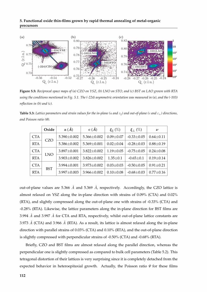
5. Functional oxide thin-films grown by rapid thermal annealing of metal-organicprecursors
(a) (b) (c)
0.79
0.77
0.75
0.73-0.56 -0.54 -0.52
Qx (r.l.u.)
Qz (
r.l.u
.) (-224)YSZ
(-224)CZO
0.80
0.79
0.78
0.77
0.76
0.75-0.27 -0.26 -0.25 -0.24
Qx (r.l.u.)
(-103)STO
(-103)LNO
0.82
0.80
0.78
0.76
0.74
-0.27 -0.26 -0.25 -0.24Qx (r.l.u.)
-0.28
(-103)LAO
(-103)BST
1
102
10
106
103
104
105
Figure 5.5: Reciprocal space maps of (a) CZO on YSZ, (b) LNO on STO, and (c) BST on LAO grown with RTA
using the conditions mentioned in Fig. 5.1. The (-224) asymmetric orientation was measured in (a), and the (-103)
reflection in (b) and (c).
Table 5.3: Lattice parameters and strain values for the in-plane (a and εk) and out-of-plane (c and ε?) directions,
and Poisson ratio (Ψ).
Oxide a (A) c (A) ξk (%) ξ? (%) ν
CTACZO
5.3900.002 5.3660.002 0.090.07 -0.330.05 0.640.11
RTA 5.3860.002 5.3690.001 0.020.04 -0.280.03 0.880.19
CTALNO
3.8970.001 3.8220.002 1.190.05 -0.750.05 0.240.08
RTA 3.9030.002 3.8260.002 1.350.1 -0.650.1 0.190.14
CTABST
3.9940.001 3.9730.002 0.030.03 -0.500.05 0.910.21
RTA 3.9970.003 3.9660.002 0.100.08 -0.680.03 0.770.16
out-of-plane values are 5.366 A and 5.369 A, respectively. Accordingly, the CZO lattice is
almost relaxed on YSZ along the in-plane direction with strains of 0.09% (CTA) and 0.02%
(RTA), and slightly compressed along the out-of-plane one with strains of -0.33% (CTA) and
-0.28% (RTA). Likewise, the lattice parameters along the in-plane direction for BST films are
3.994 A and 3.997 A for CTA and RTA, respectively, whilst out-of-plane lattice constants are
3.973 A (CTA) and 3.966 A (RTA). As a result, its lattice is almost relaxed along the in-plane
direction with parallel strains of 0.03% (CTA) and 0.10% (RTA), and the out-of-plane direction
is slightly compressed with perpendicular strains of -0.50% (CTA) and -0.68% (RTA).
Briefly, CZO and BST films are almost relaxed along the parallel direction, whereas the
perpendicular one is slightly compressed as compared to bulk cell parameters (Table 5.2). This
tetragonal distortion of their lattices is very surprising since it is completely detached from the
expected behavior in heteroepitaxial growth. Actually, the Poisson ratio Ψ for these films
112

5.2. Strain relaxation mechanisms of heteroepitaxial thin-films
(Table 5.3) reveals that their values are above Ψ=0:5 (outside the isotropic regime). This
atypical behavior has been previously reported for CZO in other thesis from our group
though it was not fully understood [114, 115]. Moreover, this distortion has also been
observed in the literature for other oxide films obtained with physical methods. Some of these
works attributed the lattice deformation to different thermal expansion coefficients between
film and substrate [210, 211]. The influence of such mechanisms will be discussed later.
Fig. 5.6 shows the HRTEM images of CZO and BST films grown with RTA at 900 ºC, 20
ºCs1 in O2 for 10 min and 5 min, respectively, and their corresponding power spectrum
(Fourier transform or FFT). The information contained in the power spectrum (FFT) confirms
that films have some degree of relaxation due to the double spot observed. Although it is
possible that dislocations act as a relaxation mechanism for these films, their presence could
not be unveiled. In this case, HRTEM image filtering was not possible because variations in
the phase caused by thickness inhomogeneities and strain created contrast modulations which
masked dislocations or produced artifacts, i. e. dislocations appeared in places where they
should not be. Therefore, if the film has a cell parameter sufficiently different from that of the
substrate, two sets of reflections will be observed in the FFT like in the case of CZO and BST
films. Typically, this implies that those films are fully or partially relaxed and the presence of
(a)
(b) (001)CZO||(001)YSZ[100]CZO||[100]YSZ
5 nm
CZO
YSZ
CZOYSZ
(001)CZO[100]||(001)YSZ[100]
BST
LAO
10 nm(001)BST[100]
||(001)LAO[100]
BSTLAO
FFT
FFT
Figure 5.6: HRTEM images and power spectrum analysis showing the presence of mismatch for (a) CZO on YSZ,
and (b) BST on LAO. Films were grown with RTA at 900 ºC, 20 ºCs1 in O2 for 5 min (BST) and 10 min (CZO).
113

5. Functional oxide thin-films grown by rapid thermal annealing of metal-organicprecursors
dislocations could be one of the relaxation mechanisms present.
Instead, LNO presents the expected behavior for films grown epitaxially on substrates
with larger lattice parameters and having a small mismatch (Table 5.2). Their in-plane cell
parameters are 3.89 A (CTA) and 3.903 A (RTA), almost matching that of STO (aSTO=3:905 A),
while the lattice is compressed along the out-of-plane direction to values below aLNObulk (Table
5.2), 3.822 A (CTA) and 3.826 A (RTA). This results in lateral tensile and perpendicular
compressive strains of 1:2% and 0:65% for CTA, and 1:4% and 0:75% for RTA, respectively.
The Poisson ratio calculated with these strains (Table 5.3) are close to the typical one for
perovskite materials (Ψ〈0.3), i. e. isotropic regime. The same trend here described has already
been reported for CSD-LSMO films grown on STO from another thesis in our group [212].
HRTEM image and power spectrum analysis of a LNO film grown on STO with RTA at 700
ºC, 20 ºCs1 in O2 for 10 min (Fig. 5.7) show that the film is strained in-plane with a lattice
constant equal to the substrate, confirming the results obtained from reciprocal space maps. In
addition, no separation between out-of-plane power spectrum spots is observed. This could
be attributed to the small difference between LNO and STO lattice constants compared to the
previous cases. Therefore, the compression suffered in the out-of-plane direction cannot be
observed.
FFT
STO
LNO LNOSTO
(001)LNO[100]||(001)STO[100]
Figure 5.7: HRTEM images, Fourier transform analysis and Fourier-filtered images of a LNO film grown on
STO. The film was grown with RTA at 700 ºC, 20 ºCs1 in O2 for 10 min.
5.2.2 Thermal expansion effects on strain relaxation
A plausible explanation for the abnormal distortion of CZO and BST cells on YSZ and LAO
substrates is that additional strains could be induced while cooling down to room temperature
due to different thermal expansion coefficients (TEC or ) [211]. A more detailed analysis of
this behavior has been performed by calculating the theoretical variation to in-plane and out-
114

5.2. Strain relaxation mechanisms of heteroepitaxial thin-films
of-plane bulk constants due to the influence of TECs (ath and cth) using [211]
Sxx = (f s) T (5.3a)
Szz = Sxx (C31 + C32) =C33; (5.3b)
and
ath = abulk (1 + Sxx) (5.4a)
cth = cbulk (1 + Szz) : (5.4b)
f and s are the linear TECs values of film and substrate, abulk and cbulk are the parallel and
normal bulk lattice parameters, and Sxx and Szz the corresponding strains. C31, C32 andC33 are
the elastic tensor constants of the film and T is the difference between annealing and room
temperatures.
In Table 5.4, we present the thermal expansion coefficients (TECs) and elastic constants
required to evaluate their contribution to strain, as well as the final lattice parameters caused by
such effect for the different heterostructures investigated. We can see that CZO is significantly
larger than Y SZ which leads to an expansion of the in-plane CZO cell constant to 5.399 A
and a compression of the out-of-plane value to 5.376 A. The lattice parameters for the in-
plane (aCZOCTA=5:390 A and aCZORTA=5:386 A) and out-of-plane (cCZOCTA=5:366 A and cCZORTA=5:369 A)
directions reported in Table 5.3 seem to be in agreement with this effect.
Likewise, BST and LAO also present similar differences between TEC values, again
resulting in the expansion of aBSTth to 4.003 A and the compression of cBSTth to 3.983 A. Again,
these cell constants are in line with those reported in Table 5.3 for the in-plane (aBSTCTA=3:994 A
and aBSTRTA=3:997 A) and out-of-plane (cBSTCTA=3:973 A and cBSTRTA=3:966 A) directions,
confirming the most probable thermal origin of such deformation. On the other hand, LNO
does not show an appreciable change in lattice parameters due to thermal effects (aLNOth =3:848
A and cLNOth =3:853 A) and the cell constants along the in-plane direction (aLNOCTA=3:897 A and
aLNORTA=3:903 A) expand to fit the substrate, while the out-of-plane ones (cLNOCTA=3:822 A and
cLNORTA=3:826 A) compress accordingly. Elastic constants used in this case have been taken from
STO (Table 5.4) since precise values for LNO were not found.
In summary, these results seem to indicate that films having relatively large compressive
mismatches and thermal expansion coefficients with the substrate like CZO on YSZ, BST on
LAO or LiNbO3 on sapphire [211] will suffer a deformation of the cell with an expansion of
the in-plane lattice parameter and a compression of the out-of-plane direction. On the other
115

5. Functional oxide thin-films grown by rapid thermal annealing of metal-organicprecursors
Table 5.4: Thermal expansion coefficients (TECs o ), elastic constants (C31, C32 and C33) and calculated
variations in lattice parameters due to thermal expansion (ath and cth). Data can be found in Refs. [94, 213–
219].
Oxide η (106 K1) (C31 +C32)/C33 ath (A) cth (A)
CZO 12.6 0.68 5.399 5.376
YSZ 9.7 - - -
LNO 8.2 0.49 3.848 3.853
STO 9.4 - - -
BST 12.9 0.96 4.003 3.983
LAO 10.0 - - -
hand, when films possess small tensile mismatches and TEC variations with substrates like
LNO or LSMO [212] on STO, they would rather prefer to stay strained and, therefore, the
behavior observed may only be associated to the expected in heteroepitaxial growth of strained
films. Finally, it would be interesting to see what would happen in other combinations of lattice
mismatchs and TECs.
5.2.3 Oxygen vacancies influence on strain relaxation
Other sources of elastic anomalies must also be considered like the presence of oxygen
deficiencies. In fact, it is known that oxygen vacancies may expand the lattice constant,
essentially, because the ionic radius of low valence ions is usually larger [220–222].
Particularly, ceria is a well-known material used for solid oxide fuel cell (SOFC)
applications due to its high ionic conductivity (i. e. oxygen diffusion), and its lattice can
sustain an exceptionally large amount of oxygen vacancies. In fact, several configurations
have been reported to show oxygen vacancies, for instance, at the surface of cerium oxide
nanoparticles [181]. We have also demonstrated in Chapter 4 that CGO nanoislands have a
considerable amount of Ce3+ ions which indicate the presence of oxygen vacancies [223].
However, their evaluation in thin films have proven much difficult and controversial. A work
in our group reported fully oxidized, i. e. a Ce4+ content of 100%, CSD-ceria films on YSZ
using XPS [108]. Moreover, we will see in Chapter 8 that EELS analysis of CZO films prepared
by FIB are fully oxidized. Nevertheless, Song et al. reported very recently a high deficiency of
oxygen at the interface of ceria films grown on (111)YSZ by PLD, while the rest remained fully
116

5.2. Strain relaxation mechanisms of heteroepitaxial thin-films
oxidized [179]. Ceria has such good ionic conductivity that the amount of oxygen vacancies in
its structure it is very likely to be affected by the preparation and measurement techniques
employed.
Oxygen vacancies in LNO have been measured using electron diffraction and evaluating
the oxidation state of Ni cations [224]. Later, Sánchez et al. correlated the metal-insulator
transition for LaNiO3x which becomes non-conductive when oxygen stoichiometry is
reduced beyond x=0:25 [221]. Resistivity measurements for our LNO films grown on STO
using the methodology described in Appendix A.4.4 (Fig. 5.8) show that they are highly
metallic suggesting that the number of vacancies must be below the aforementioned value if
there are any. Additionally, resistivity values are equivalent to those reported in the literature
for samples produced from chemical or physical techniques [221, 225, 226].
0 50 100 150 200 250 3000
10-4
2·10-4
3·10-4
4·10-4
5·10-4
Res
istiv
ity (Ω
·cm
)
Temperature (K)
RTA (700 ºC
, 20 ºC·s-1 ,
15 min)
CTA (700 ºC, 10 º
C·min-1 , 1 h)
Figure 5.8: Resistivity measurements for LNO on STO. Films were grown using RTA (red circles) and CTA (blue
squares) at 700 ºC, 20 ºCs1 for 15 min and 700 ºC, 10 ºCmin1 for 1 h, respectively, in O2.
Although no direct evidence of oxygen reduction have been found for BST, it has been
reported that this system undergoes a dielectric relaxation which has been linked to the
existence of oxygen vacancies [227–229]. Essentially, measurement of the dielectric response
for BST films showed a drastic increase of the dielectric constant and loss above 200 ºC; a
phenomenon attributed to the displacement of vacancies which behave as polarons when an
external AC electric field is applied [230]. Regardless, room temperature piezoresponse force
microscopy (PFM) measurements for a BST film at 900 ºC, 10 ºCmin1 for 4 h in O2 (Fig. 5.9a)
show that it is possible to write two square domains, at +7 V (outter square) and -7 V (inner
square), with inverse polarization. Additionally, hysteresis loops of amplitude and phase
(Figs. 5.9b and c) have been recorded, indicating a piezo/ferroelectric behavior in the film.
117

5. Functional oxide thin-films grown by rapid thermal annealing of metal-organicprecursors
The quality factor Q and remanence d33 values, calculated as explained in section A.4.6, for an
AC voltage of 2.5 V are Q〈80 and d33〈25 pmV1. Remanence d33 is well below the bulk
value (dBTO;bulk33 〈190 pmV1 [231]) and slightly lower than the range of values reported for
BaTiO3 in the literature (30-100 pmV1 [232, 233]). However, it must be noticed that films in
the literature are thicker than our films and d33 values have been reported to increase with
film thickness [234].
(b)
-8 -6 -4 -2 0 2 4 6 80.0
0.1
0.2
0.3
Am
plitu
de (
nm)
Sample Bias (V)-8 -6 -4 -2 0 2 4 6 8
Sample Bias (V)
0306090
120150
180
Phas
e (º
)
(c)(a)
+7 V
-7 V
Figure 5.9: Piezoresponse Force Microscopy (PFM) measurements of a BST film annealed at 900 ºC, 20 ºCs1
for 30 min in O2. (a) PFM phase image showing the written domains with a voltage of +7 V (outter square) and
-7 V (inner square). Hysteresis loops are representative of (b) amplitude and (c) phase.
Despite unequivocal evidence of vacancies has not been found and further
characterization using less invasive compositional techniques (XAS, XANES, EXAF, etc)
would be required to precisely determine the oxidation state of these films, it is very likely
that our samples are oxygen reduced to some extent, and thus, the lattice parameter is
modified accordingly. Although this may have some contribution in our films, we can
conclude that different thermal expansion coefficients between film and substrate is the main
contribution to strain relaxation for CZO and BST films on YSZ and LAO, while LNO films on
STO may be only influenced by heteroepitaxial strain since their TECs are very similar and no
significant oxygen vacancies are expected.
5.3 Growth of oxide thin films by CSD
In this section, we will investigate the different stages that lead to the formation of the fully
epitaxial thin films described in previous sections. In first place, we will analyze the initial
state of the films right after decomposition, experimentally and theoretically, and compare it
with that of CGO nanoislands. Later, we will study the kinetic evolution of single deposition
and multicoatings (3 depositions) of CZO as a model case, and compare it with more complex
118

5.3. Growth of oxide thin films by CSD
oxide heterostructures investigated, i. e. LNO and BST films on STO and LAO, respectively.
The morphological and epitaxial evolution will be described, as well as the structural and
microstructural characteristics. Furnace annealing have been used for comparison with RTA
studies.
5.3.1 Study of CSD-pyrolyzed precursor films
The general belief in CSD is that after deposition and decomposition of metal-organic
precursors, films consists of amorphous or nanocrystalline precursor oxide phases [10, 56].
However, we demonstrated in Chapter 4 that in the case of CGO precursors there exists
already a driving force to crystallization and even epitaxial growth at 300 ºC. In addition,
Roura et al. have reported that fully decomposed and polycrystalline ceria films can be
produced at temperatures below 200 ºC by employing long annealing times (〈1 h) [122]. In
our case, we decomposed CZO, LNO and BST films at temperatures of 300, 350 and 450 ºC,
respectively, in order to keep the pyrolysis time between 10 and 30 min. The selection of
temperatures was done from thermogravimetric measurements of powder samples as it has
been explained in section 2.3.1. Nevertheless, it must be considered that thin-films will be
decomposed at lower temperatures or faster than powder samples since decomposition
involves diffusion and transport limited processes [122]. Decomposition was assured through
Fourier-transform infrared (FTIR) spectroscopy analyses as detailed in Appendix A.1.1.
The morphological characterization illustrated in Fig. 5.10 shows extremely flat surfaces
with roughness below 0.5 nm of CZO, LNO and BST films pyrolyzed on YSZ, STO and LAO,
respectively, for 10 min (BST) and 30 min (CZO and LNO) at the temperatures mentioned
before. It is worth mentioning that decomposition of CZO propionate precursors involves a
(a) (b) (c)
0.25 µmRMS=0.3 nm
300 ºC, 30 min
0.25 µmRMS=0.4 nm
350 ºC, 30 min
0.25 µmRMS=0.3 nm
450 ºC, 10 minCZO on YSZ LNO on STO BST on LAO
Figure 5.10: AFM images of pyrolyzed films of (a) CZO on YSZ, (b) LNO on STO, and (c) BST on LAO.
Decomposition was done in a pre-heated furnace at 300, 350 and 450 ºC. Pyrolysis times were 30 min for CZO
and LNO, and 10 min for BST.
119

5. Functional oxide thin-films grown by rapid thermal annealing of metal-organicprecursors
transition to a molten state [121], i. e. starts at temperatures close to their melting point (〈235
ºC). Although this phenomenon may be irrelevant for the slow decomposition performed with
thermal treatments, we will show in chapter 7 that it will affect the final surface morphology
when employing extremely faster pulsed laser treatments.
XRR measurements shown in Fig. 5.11 allow us to obtain the thickness of the different
films after decomposition and prior to crystallization. Table 5.5 shows that thicknesses are
〈26 nm, 〈39 nm and 〈43 nm for CZO, LNO and BST, respectively. After high-temperature
crystallization at their corresponding experimental conditions (section 5.1), films will
experience a densification between 20-35% (Table 5.5).
The structural characterization of these pyrolyzed films to identify their crystalline state
has proven rather complicated. For CZO, we expected that the film would be composed of
random polycrystalline nanograins with a minimum size [122], and a tiny amount of epitaxial
grains at the interface (section 4.3.1). Typical 2 measurements (Fig. 5.12a) were only able
LNO
CZO
0.5 1.0 1.5 2.0 2.5 3.0
103
Inte
nsity
(a.
u.)
10
105
107
Grazing angle (º)
102
104BST
Figure 5.11: X-ray reflectometry of CZO (—), LNO (—) and BST (—) pyrolyzed films. Decomposition was done
in a pre-heated furnace at 300, 350 and 450 ºC. Pyrolysis times were 30 min for CZO and LNO, and 10 min for
BST.
Table 5.5: Thicknesses of CZO, LNO and BST films after decomposition and prior to crystallization. The degree
of densification reached after high-temperature annealing has been calculated considering the values from Table
5.1.
Oxide Thickness (nm) Densification (%)
CZO 26.23.3 25
LNO 38.74.6 35
BST 42.55.8 20
120

5.3. Growth of oxide thin films by CSD
(a) (b) (c)
20 25 30 35 40 45
102
103
104
Inte
nsity
(a.
u.)
10
105
-2 (º)
106
1 layer
3 layers
YSZ kβ
(002)YSZ
(111)CZO
300 ºC,90 min (002)YSZ
(111)CZO20 25 30 350
2
4
6
8CZO(111)
Cou
nts
(a.u
.) YSZ(002)
-2 (º)
3 layers,90 min
1 layer,90 min
300 ºC, 30 min(1 layer)
300 ºC
1 layer,30 min
Figure 5.12: XRD measurements of CZO thin films on YSZ. (a) 2 representation of films (1 and 3 layers)
annealed during 90 min. (b) 2D-XRD image of a single-layered film pyrolyzed for 30 min, and (c) corresponding
2 representation including 1-layered and 3-layered films pyrolyzed for 90 min. Specific conditions used to
reduce substrate's contribution are described in section A.3.1.
to detect the commented polycrystalline (111)CZO reflection for 3-layered films pyrolyzed at
300 ºC for 90 min. In order to detach the film from substrate contribution and see more clearly
if polycrystalline or epitaxial material was present, 2D-XRD measurements were performed
using especial conditions to eliminate substrate’s contribution as described in section A.3.1.
Integration of the 2D image (Fig. 5.12b) allows us to see a small peak whose intensity increases
with the pyrolysis time from 30 to 90 min, and with thickness from 1 to 3 layers (Fig. 5.12c). In
addition, an approximate determination of the particle size was calculated using the Scherrer
formula (section A.3.2). Table 5.6 shows that particles are really small after 30 min of pyrolysis
with sizes of 〈2 nm. Particle dimensions slightly enlarged to 〈4 nm after 90 min of treatment,
and to 〈6 nm if the number of coatings is increased from 1 to 3 layers. In turn, this leads to an
increase of the surface roughness from 0.3 to 0.4 and 0.7, respectively, and indicates a moderate
coarsening of the polycrystalline nanograins at the pyrolysis conditions when long times are
used.
For LNO films, there is no evidence of polycrystalline or epitaxial growth from XRD
measurements (Fig. 5.13). Characterization by HRTEM could not be done after several trials
Table 5.6: Particle size and RMS roughness of pyrolyzed CZO thin-films.
Depositions Particle size (nm) RMS roughness (nm)
1 layer (30 min) 22 0.3
1 layer (1h 30 min) 42 0.4
3 layers (1h 30 min) 61 0.7
121

5. Functional oxide thin-films grown by rapid thermal annealing of metal-organicprecursors
(a) (b)350 ºC, 90 min(1 layer)
STO kβ
(002)STO
20 25 30 35 40 45 500
5
10
15
20
25
Cou
nts
(a.u
.)
-2 (º)
3 layers, 90 min
1 layer,90 min
350 ºC
STO kβ
(002)STO
(011)LNO(002)LNO
Figure 5.13: XRD measurements of LNO thin films on STO. (a) 2D-XRD image of a single-layered film pyrolyzed
at 350 ºC for 90 min, and (b) corresponding 2 representation including a 3-layered film pyrolyzed with the
same duration.
due to problems during specimen preparation. Therefore, we expected the film to consists of
amorphous material, and thus, we used the pyrolysis conditions commented before (350 ºC
and 30 min).
Similar results were found for BST films where no crystalline peaks could be identified
(Figs. 5.14a and b). Surprisingly, HRTEM analysis of a film pyrolyzed at 450 ºC for 30 min (Figs.
5.14c-e) reveals that there is a considerable amount of epitaxial BST grains at the interface, in
(a) (b)
LAO kβ
(002)LAO
450 ºC, 30 min(1 layer)
20 25 30 35 40 45 500
5
10
15
20
25
Cou
nts
(a.u
.)
-2 (º)
3 layers,30 min
1 layer,30 min
450 ºC
LAO kβ
(002)LAO
BST
LAO50nm
40 nm
Epitaxial
Amorphous~(c)
BST
LAO
(d)
[001]LAO||[001]BST
(100)
(0-10)
(e)
(011)BST(002)BST
Figure 5.14: XRD measurements of BST thin films on LAO: (a) 2D-XRD image of a single-layered film pyrolyzed
at 450 ºC for 30 min, and (b) corresponding 2 representation including a 3-layered film pyrolyzed with the
same duration. HRTEM characterization of a pyrolyzed film at 450 ºC for 30 min (c) and (d), and (e) corresponding
power spectrum analysis.
122

5.3. Growth of oxide thin films by CSD
some cases being as high as the film thickness, and the rest of the film remains amorphous with
no polycrystalline crystallization. The total amount of epitaxial material must be rather small
since it could not be detected by XRD. Additionally, some degree of relaxation of the epitaxial
grains has been identified from the two separated spots in the corresponding power spectrum
analysis (Fig. 5.14e).
Contrarily to what Schneller et al. comment [56], no precursor phases were found prior
to the final phase crystallization. The most probable explanation for this event is that the rate
for heterogeneous nucleation dominates over homogeneous nucleation, even though at low
temperatures both events may have very similar probability to occur (Chapter 3). In order to
diminish the presence of epitaxial BST at this early stage, the pyrolysis time for the upcoming
results was reduced to 10 min.
5.3.2 Thermodynamic analysis of CSD films’ nucleation
We now want to address the type of nucleation that should be expected in CZO, LNO and BST
thin films on YSZ, STO and LAO substrates, respectively, from the thermodynamic point of
view.
The usual description to predict the growth mode is based on the simple analysis of surface
energies between substrate s, interface i and film f (Section 3.1). We have taken f〈 100
since it is the film orientation we are crystallizing. It can be seen from Table 5.7 that CZO films
should present a 3D growth provided s< i+ f , while the growth mechanism for LNO and
BST should be 2D because s> i+ f .
The case of doped-CeO2 has been described in depth in Chapter 4 and HRTEM images of
Table 5.7: Energies of the (100) surfaces and interface energies of the different heterostructures investigated
[39, 167–169, 235–237].
Oxide γ100 surface energy (J/m2) Interface energy γi
CZO 3.25Low (fluorite on fluorite)
YSZ 1.75
LNO 1Low (perovskite on perovskite)
STO 1.2
BST 1.13Low (perovskite on perovskite)
LAO 1.58
123

5. Functional oxide thin-films grown by rapid thermal annealing of metal-organicprecursors
partially grown films confirm the 3D growth (Fig. 5.15a, and 5.22b from section 5.3.4). Fig.
5.15b seems to confirm that the growth mode for LNO films on STO is indeed 2D because
the truncated pyramid-shaped grains have not been observed. In addition, an ultra-diluted
LNO solution (0.04 M) has been employed to confirm the growth mode for LNO. If after high
temperature annealing the system had split into islands then growth would have been 3D as
in doped-CeO2. However, it can be seen in Fig. 5.16 that LNO follows the substrate steps and
no nanoislands are present, which again corroborates the 2D growth mode. The separation of
the LNO film at the substrate steps is still unclear. However, similar results were reported on
(001)STO substrates due to the selective growth of different chemical terminations, i. e. SrO
and TiO2, after high temperature and long time treatments (1100 ºC for 30 min) [238, 239].
Despite this two cases can be explained just with the relation between surface energies,
BST films on LAO seem to follow a 3D growth instead of the expected 2D one (Fig. 5.14c). It
has been mentioned in section 3.2.2 that strain can have a relevant influence in nucleation if
(b)(a)
Polycrystalline LNO
Epitaxial LNOSTO
YSZEpitaxial CZO
Polycrystalline CZO
Figure 5.15: HRTEM images showing the growth mode of: (a) CZO film on YSZ, and (b) LNO on STO. Samples
were grown at 20 ºCs1 for 10 min in O2 with RTA. The annealing temperatures of CZO and LNO were 900 ºC
and 700 ºC, respectively.
(b)
0.25 µm
(a)
0.0 0.2 0.4 0.6 0.8 1.0 1.2 1.40246
Hei
ght
(nm
)
Width (µm)
Figure 5.16: (a) AFM image and (b) corresponding line scan of an ultra-diluted LNO film grown on STO. The
solution concentration was adjusted to 0.04 M. Growth was done at 700 ºC, 10 ºCmin1 for 1 h in O2 using a
CTA furnace.
124

5.3. Growth of oxide thin films by CSD
its contribution is large enough, and thus, it could explain the transition between 2D and 3D
growth. If we consider the lattice mismatch between film and substrate for each heterostructure
(Table 5.2), it can be observed that LNO films have a relatively low mismatch which should
lead to a strain energy small enough to prevent a 3D growth. Oppositely, CZO and BST should
possess a considerable strain energy due to the large mismatch with their respective substrates.
A 3D mode should already be expected for CZO, but it seems feasible that BST nucleation
changes from 2D to 3D nucleation.
5.3.3 Isothermal grain coarsening in CSD oxide films
Functional properties are known to be strongly influenced by film microstructure [24, 188].
Therefore, it is important to understand how films’ morphology evolves with the annealing
time in order to produce devices with high performance.
Fig. 5.17 presents the AFM characterization for the three oxide films (CZO, LNO and BST)
grown with rapid thermal annealing at 20 ºCs1 in O2 after 1, 5, 15 and 30 min of annealing at
the optimal temperatures for each oxide (900 ºC for CZO and BST, and 700 ºC for LNO). A
detailed analysis of the morphological evolution (Fig. 5.18) reveals that film’s roughness
decreases with time as grain size increases. Initially, one should expect a rise in films’
roughness with grain coarsening if spherical grains are present together with a corresponding
larger peak-to-valley difference [113, 240–242]. However, the kinetic evolution of grains is also
accompanied by grain boundary zipping processes and atomic mobility, i. e. reduction of
grain boundaries and porosity [243], and more importantly the formation of flat terraces
common in epitaxial growth due to energy minimization mechanisms [194], which lead to a
reduction in roughness. The larger roughness of BST films compared to that of CZO and LNO
films could be either linked to the larger grain size or to the presence of a bimodal distribution
of grains as shown in section 5.1, where some amount of taller grains easily augment film’s
roughness. Although one could suspect that these grains are polycrystalline, no evidence was
found as we will show later.
Besides, several authors have reported a self-limiting grain growth behavior for various
oxide films [159, 161, 244] leading to a saturation of grain sizes after a certain annealing time.
Fig. 5.18b seems to reflect a slight trend towards saturation but since grain sizes are still far
from those obtained with CTA (Fig. 5.1), we expect some increase in dimensions until
saturation is reached.
Fig. 5.19a shows the relaxation times for RMS roughness and grain size. We have calculated
125

5. Functional oxide thin-films grown by rapid thermal annealing of metal-organicprecursors
0.25 µm0.25 µm0.25 µm 0.25 µm
0.25 µm0.25 µm0.25 µm 0.25 µm
0.25 µm 0.25 µm0.25 µm0.25 µm
900 ºC
CZO
||YSZ
LN
O||S
TO
BST
||LA
O
(a)
(b)
(c)
1 min 15 min 30 min5 min900 ºC 900 ºC 900 ºC
700 ºC700 ºC 700 ºC 700 ºC
900 ºC900 ºC 900 ºC 900 ºC
RMS=1.4 nm
RMS=1.1 nm
RMS=1.1 nm
RMS=0.7 nm
RMS=1.5 nm
RMS=0.7 nm
RMS=0.8 nm
RMS=0.7 nm
RMS=4.3 nm
RMS=6.5 nm
RMS=3.6 nm
RMS=3.0 nm
Figure 5.17: AFM images depicting the morphological evolution at 1, 5, 15 and 30 min of: (a) CZO on YSZ, (b)
LNO on STO, and (c) BST on LAO. Growth was done with RTA at 20 ºCs1 in O2. Annealing temperatures
were 900 ºC (CZO and BST) and 700 ºC (LNO).
(a) (b)
0.51.01.53.04.56.07.5
0 5 10 15 20 25 30
RM
S (n
m)
Annealing Time (min)
CZO
LNO
BST
0153045607590
Mea
n gr
ain
size
(nm
)
0 5 10 15 20 25 30Annealing Time (min)
105
CZO
LNO
BST
Figure 5.18: Time evolution of (a) roughness and (b) mean grain size of CZO, LNO and BST thin films grown
on YSZ, STO and LAO substrates obtained from AFM images. Films growth has been carried out as indicated in
Fig. 5.17.
126

5.3. Growth of oxide thin films by CSD
(a) (b)
CZO LNO BST0
250
500150017502000
Rel
axat
ion
time
(s)
Grain size
RMS
CZO LNO BST0
2
4
6
8
10
In-p
lane
diff
.co
eff.,
D|| (
10-1
9 m2 ·s
-1)
CGO NDs on YSZ
Figure 5.19: (a) Relaxation times of RMS roughness and grain size, and (b) in-plane diffusion coefficients of CZO
on YSZ, LNO on STO and BST on LAO thin-films.
the relaxation times for the RMS (θRMS) using a decay exponential function
RMS(t) = RMSr +RMS0 exp (t=θRMS) ; (5.5)
whereRMS0 andRMSr are the initial and residual RMS, respectively. The grain size relaxation
times (θGS) have been calculated employing the aforementioned self-limited growth behavior
(Eq. 3.22). θRMS values can be found between 240 and 350 seconds which indicate a quite fast
RMS decrease with time for the different cases. Despite that, θCZOGS is larger than θLNOGS and
θBSTGS meaning that the time needed to reach the maximum grain size is significantly longer.
Additionally, we have calculated the in-plane diffusion coefficients for the different
heterostructures at their corresponding annealing temperatures (Eq. 3.23) using the relaxation
times reported. In Fig. 5.19b, the diffusion coefficient of CZO (DCZOk ) has the same value as
the one obtained from the coarsening of nanodots DNDsk (section 4.4). In fact, similar diffusion
values were expected since they present equivalent heteroepitaxial and chemical
arrangements. These values are one order of magnitude larger than those reported in the
literature for polycrystalline CGO films [159] which is in agreement with the data we will
present later for our case. We can also see that the diffusion coefficient of LNO (DLNOk ) is
slightly smaller than DCZOk . This indicates that LNO atomic mobility is quite important, even
though the annealing temperature used is lower (i. e. 700 ºC in LNO and 900 ºC in CZO).
Finally, the diffusion coefficient of BST (DBSTk ) is well above the other values implying a
considerably larger atomic mobility. This was initially unexpected and in fact there are no
reports on this matter, but it is very appealing for applications based on BST films.
Apart from the time evolution of surface morphology, an enlargement of grain size and
consequent roughness increase have been reported to depend on film thickness [191]. Thicker
127

5. Functional oxide thin-films grown by rapid thermal annealing of metal-organicprecursors
CZO, LNO and BST films have been prepared following the multideposition procedure
explained in section 2.3.1 and annealed with RTA at 900 ºC (CZO and BST) and 700 ºC (LNO).
Figs. 5.20a-c show the change in film surfaces after 3 multidepositions. The films’ thicknesses
are expected to be around 60 nm for CZO, 70 nm for LNO and 100 nm for BST.
As it can be seen, surfaces have lost the flat-terraced aspect of single coatings and are
composed of granular grains that can be associated to polycrystalline phases as we will see in
the next section. The first consequence is that films’ roughness has experienced a considerable
increase; from 0.71 to 2.06 nm for CZO, 0.68 to 2.97 nm for LNO and 2.99 to 4.91 nm for BST
(Fig. 5.20d). This effect is related to the aforementioned presence of spherical-like grains
instead of flat terraces. The reduction in grain sizes compared to single coatings (Fig. 5.20e) is
uncommon, but it can be attributed to the presence of polycrystalline grains which have
0.25 µm0.25 µm
0.25 µm0.25 µm
0.25 µm0.25 µmRMS=2.1 nmC
ZO
||YSZ
LN
O||S
TO
BST
||LA
O
(a)
(b)
(c)
30 min 1 h
RMS=2.0 nm
RMS=3.0 nm
RMS=2.8 nm
RMS=4.8 nm
RMS=4.9 nm
(d)
30 35 40 45 50 55 601
2
3
4
5
RM
S (n
m)
Annealing Time (min)
BST (1 layer)
CZO (1 layer)LNO (1 layer)
BST(3 layers)
LNO (3 layers)
CZO (3 layers)
(e)
900 ºC 900 ºC
700 ºC700 ºC
900 ºC900 ºC
20
40
60
80
100
30 35 40 45 50 55 60
Gra
in s
ize
(nm
)
Annealing Time (min)
BST (1 layer)
CZO (1 layer)LNO (1 layer)
BST (3 layers)
CZO (3 layers)LNO (3 layers)
Figure 5.20: AFM images of (a) CZO on YSZ, (b) LNO on STO, and (c) BST on LAO for films with 3
multidepositions, after 30 min and 1 h of annealing at 900 ºC (CZO and BST) and 700 ºC (LNO). (d) Roughness
and (e) grain size dependence with the annealing time extracted from AFM for CZO (open orange circles), LNO
(open green triangles) and BST (open red squares). The optimum values obtained for single layers are represented
with full symbols.
128

5.3. Growth of oxide thin films by CSD
smaller sizes than the epitaxial terraced part of a single layer (Fig. 5.18b).
5.3.4 Experimental and theoretical description of the epitaxial transformation
In section 5.3.1 we have seen that it is possible to achieve some degree of crystallinity and even
epitaxy after decomposition at very low temperatures. Nevertheless, the crystalline quality is
rather poor and, as we demonstrated in section 5.1, high temperature annealing will promote
epitaxial crystallization further.
As we mentioned in section 3.2.1, the formation of a crystalline phase from amorphous
material is governed by the reduction in the Gibbs free energy between the initial and final
stages Gv (Fig. 3.4). At high temperatures we expect all the material to be in a crystalline
form, hence, the transformation from polycrystalline to epitaxial phases should be driven by
grain boundary (GB) recrystallization, reduction of low-angle GB, or the formation of terraced
surfaces most of which will be controlled by atomic diffusion.
2 measurements for the single-deposited oxide heterostructures analyzed, i. e. CZO on
YSZ, LNO on STO and BST on LAO, show that the intensity of the epitaxial (002) reflection
increases with annealing time (Figs. 5.21a, c and e). This tendency is more evident for films
grown using RTA since the initial crystalline intensity is rather poor, probably due to the faster
heating ramps. In addition, a small peak corresponding to the most intense polycrystalline
orientation of each heterostructure, i. e. (111)CZO, (011)LNO and (011)BST, is identified for
samples grown by RTA when short annealing times are used, typically below 10 min. This
demonstrates the presence of randomly oriented grains which will probably have spherical
shapes, as we mentioned previously. Multi-layered films obtained after three depositions and
consecutive pyrolysis following the methodology explained in section 2.3 show rather similar
epitaxial intensities (Figs. 5.21b,d and f). However, the polycrystalline peak is more intense
compared to single-layered films. Altogether, this seems to suggest that there exists a strong
driving force to transform the highly energetic polycrystalline phase into an ordered epitaxial
film promoted by the substrate, which we will further evaluate in this section.
In agreement with the results shown in section 5.2, CZO and BST films show inappreciable
variations of their (002) peak position demonstrating a relaxed state even at short annealing
times (Figs. 5.21a, b, e and f). In contrast, a shift towards higher angles which increases with
the annealing time has been detected for the (002) reflection of LNO films (Figs. 5.21c and d).
This displacement can be attributed to the heteroepitaxial growth behavior described in section
5.2, where a film having insignificant thermal differences with the substrate and a small tensile
129
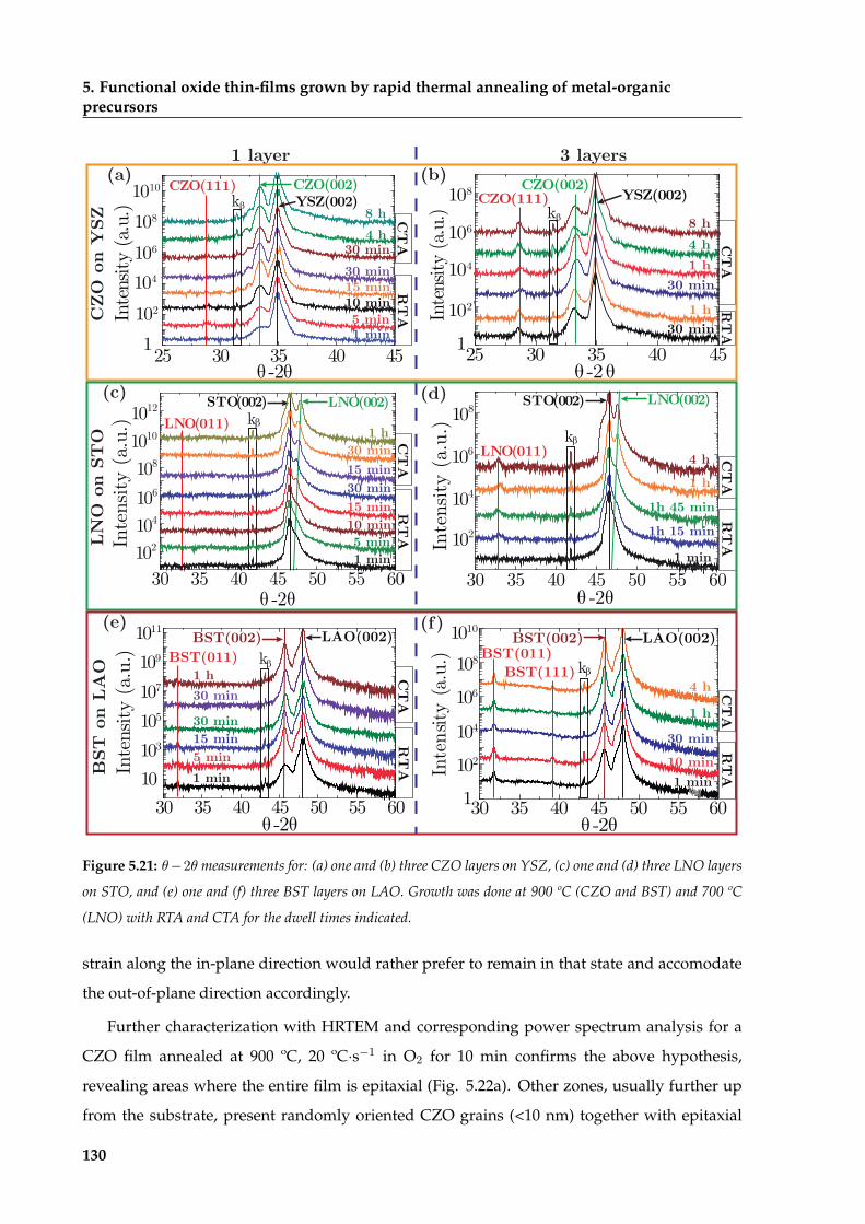
5. Functional oxide thin-films grown by rapid thermal annealing of metal-organicprecursors
(a) (b)
25 30 35 40 45 -2
1
102
104
106
108 YSZ(002)
Inte
nsity
(a.u
.)
CZO(002)CZO(111)
4 h
1 h30 min
1 h
kβ
RT
A
30 min
CT
A
8 h
1102
104
106
108
Inte
nsity
(a.u
.)
1010
25 30 35 40 45 -2
YSZ(002)CZO(002)CZO(111)
4 h
kβ
RT
A
30 min
CT
A
30 min
8 h
15 min10 min5 min1 min
1 layer 3 layers
(c) (d)
102
104
106
108
1010
-2
STO(002) LNO(002)LNO(011)
5 min
kβ
RT
A15 min
CT
A
10 min
30 min
30 min1 h
15 min
1 min30 35 40 45 50 55 60
Inte
nsity
(a.
u.)
1012
-2
30 35 40 45 50 55 60
Inte
nsity
(a.
u.)
102
104
106
108 STO(002) LNO(002)
LNO(011)
1h 45 min
kβ
RT
AC
TA
4 h
1h 15 min
1 h
1 min
(e) (f)
30 min
30 min1 h
15 min5 min
BST(002)
RT
AC
TA
10103
105
107
109
-230 35 40 45 50 55 60
Inte
nsity
(a.
u.)
1011
kβBST(011)LAO(002)
1 min
RT
AC
TA
t
30 35 40 45 50 55 60
Inen
sity
(a.u
.)
102
104
106
108
1
1010
-2
BST(002)BST(011)
LAO(002)
kβBST(111)
1 h
4 h
30 min
10 min1 min
LN
O o
n ST
OC
ZO
on
YSZ
BST
on
LA
O
Figure 5.21: 2 measurements for: (a) one and (b) three CZO layers on YSZ, (c) one and (d) three LNO layers
on STO, and (e) one and (f) three BST layers on LAO. Growth was done at 900 ºC (CZO and BST) and 700 ºC
(LNO) with RTA and CTA for the dwell times indicated.
strain along the in-plane direction would rather prefer to remain in that state and accomodate
the out-of-plane direction accordingly.
Further characterization with HRTEM and corresponding power spectrum analysis for a
CZO film annealed at 900 ºC, 20 ºCs1 in O2 for 10 min confirms the above hypothesis,
revealing areas where the entire film is epitaxial (Fig. 5.22a). Other zones, usually further up
from the substrate, present randomly oriented CZO grains (<10 nm) together with epitaxial
130

5.3. Growth of oxide thin films by CSD
truncated pyramids, typical of 3D growth (Figs. 5.22b and c). This suggests that longer
annealing times must be used in order to obtain fully epitaxial films. Similar studies were
done for a LNO film annealed at 700 ºC, 20 ºCs1 for 10 min in O2. We can see that most of
the film is epitaxial with some places reaching the whole film thickness (Figs. 5.22d and e).
Nevertheless, there is still an important amount of polycrystalline grains present (Figs. 5.22d
and f). As we mentioned before, further annealing of these films should allow us to achieve
full epitaxy. Surprisingly, HRTEM investigations for a BST film annealed at 900 ºC, 20 ºCs1
(001)BST[100]||(001)LAO[100]
(b)
YSZCZO
Epitaxial film(∼15 nm)
(a)
Polycrystalline CZO
(001)CZO[100]||(001)YSZ[100]
YSZCZO
10 nm
(c)
Polycrystalline LNO
Epitaxial LNO
STO(001)LNO[100]
||(001)STO[100]
(d) (e) (f)Polycrystalline LNO
(h)(g) (i)
10 nm
LAOBST
Epitaxial film(∼30 nm)
LN
O o
n ST
OC
ZO
on
YSZ
BST
on
LA
O
25 nm
Figure 5.22: HRTEM characterization for a CZO film grown on YSZ at 900 ºC, 20 ºCs1 for 10 min in O2. Two
different areas of the same sample are presented: (a) completely epitaxial zone, and (b) partially polycrystalline
area, and (c) corresponding FFT analysis. HRTEM characterization for a LNO film grown on STO at 700 ºC, 20
ºCs1 for 10 min in O2: (d) image, (e) and (f) power spectra of epitaxial and polycrystalline regions, respectively.
HRTEM characterization for a BST film grown on LAO at 900 ºC, 20 ºCs1 for 5 min in O2: (g) large area and
(h) small area images, and (i) corresponding FFT analysis.
131

5. Functional oxide thin-films grown by rapid thermal annealing of metal-organicprecursors
in O2 for 5 min reveal a completely epitaxial film. This shows that BST definitely has a faster
epitaxial growth rate than the previous heterostructures (Figs. 5.22g-i).
Despite these appealing results, common 2 XRD measurements are inadequate to
evaluate the ratio between epitaxial and random crystallization because they only provide
out-of-plane information and the size of crystallites have an important contribution to its
intensity. Furthermore, HRTEM characterization is a quite local technique and, therefore, a
more general investigation is needed. In order to obtain a more accurate quantitative analysis,
we have used a methodology based on 2D-XRD employed previously in the group [5, 245]
and described in Appendix A.3.1. Fig. 5.23 shows the quantification of the epitaxial fraction
for single- and multi-layered films, and two examples of the 2D-XRD data acquired for the
different oxide heterostructures studied. In single-coated films the epitaxial fraction increases
rapidly at expenses of polycrystalline material, and heteroepitaxial growth has been
completed after 〈15-30 min of annealing with RTA. Films treated using CTA are always
epitaxial for the times investigated. On the other hand, multi-layered films present a slower
epitaxial transformation (Figs. 5.23a, d and g). It must be emphasized that, to the extent of our
knowledge, this is the first time an epitaxial growth mechanism is proposed to be originated
from the transformation of a polycrystalline film of the same phase. The different aspects
contributing to this conversion will be discussed next.
The transformation rate can be extracted by fitting the results from Fig. 5.23 with a self-
limited growth model (Eq. 3.22). Fig. 5.24a shows that the characteristic relaxation times for
the epitaxial conversion (defined in section 3.3) follow the trend θBSTepi <θLNOepi <θCZOepi , i. e. the
epitaxial transformation rate for BST is faster than LNO and CZO as we had foreseen from
HRTEM analyses. This trend has also been observed in thicker films (Fig. 5.24a). However, the
epitaxial growth time for multi-layered films is around two orders of magnitude slower which
evidences a reduction in the transformation rate of the overall process.
The calculation of the epitaxial diffusion coefficients presented in Fig. 5.24b has been done
applying Eq. 3.23, using the typical thicknesses of the different oxide films (sections 5.1 and
5.3.3), and their corresponding relaxation times extracted from data fitting in Fig. 5.23. Notice
that the epitaxial diffusion coefficient of BST (DBSTepi ) is more than three times larger thanDLNO
epi
andDCZOepi . This trend is similar to that of θepi and it is preserved for thicker films. Furthermore,
there is around one order of magnitude difference between the diffusion coefficients of single-
and multi-layered films.
An additional way to characterize these results is through the evaluation of the epitaxial
132
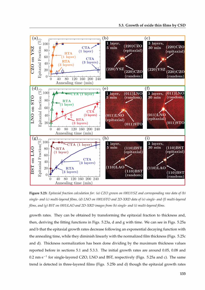
5.3. Growth of oxide thin films by CSD
(a) (b) (c)1 layer,5 min
(220)YSZ(220)CZO(random)
(220)CZO(epitaxial)
3 layers, 30 min
(220)YSZ (220)CZO(random)
(220)CZO(epitaxial)
(d) (e) (f)1 layer,5 min
(011)LNO(random)
(011)LNO(epitaxial)
(011)STO
3 layers, 30 min
(011)LNO(random)
(011)LNO(epitaxial)
(011)STO
(g) (i)1 layer,5 min
(110)BST(random)
(110)BST(epitaxial)
(110)LAO
3 layers, 30 min
(110)BST(random)
(110)BST(epitaxial)
(110)LAO
LN
O o
n ST
OC
ZO
on
YSZ
BST
on
LA
O
(h)
0 40 80 120 160 200 2400
20
40
60
80
100
Epita
xial
Fra
ctio
n(%
)
Annealing time (min)
CTA (1 layer)RTA
(1 layer)
RTA(3 layers)
CTA(3 layers)
0 40 80 120 160 200 24020
40
60
80
100
Epita
xial
frac
tion
(%)
Annealing time (min)
CTA (1 layer)
RTA(3 layers)
CTA(3 layers)
RTA(1 layer)
0 40 80 120 160 200 2400
20
40
60
80
100
Ep
itaxi
al F
ract
ion
(%)
Annealing time (min)
CTA(1 layer)
RTA(3 layers)
CTA(3 layers)
RTA(1 layer)
Figure 5.23: Epitaxial fraction calculation for: (a) CZO grown on (001)YSZ and corresponding raw data of (b)
single- and (c) multi-layered films, (d) LNO on (001)STO and 2D-XRD data of (e) single- and (f) multi-layered
films, and (g) BST on (001)LAO and 2D-XRD images from (h) single- and (i) multi-layered films.
growth rates. They can be obtained by transforming the epitaxial fraction to thickness and,
then, deriving the fitting functions in Figs. 5.23a, d and g with time. We can see in Figs. 5.25a
and b that the epitaxial growth rates decrease following an exponential decaying function with
the annealing time, while they diminish linearly with the normalized film thickness (Figs. 5.25c
and d). Thickness normalization has been done dividing by the maximum thickness values
reported before in sections 5.1 and 5.3.3. The initial growth rates are around 0.05, 0.08 and
0.2 nms1 for single-layered CZO, LNO and BST, respectively (Figs. 5.25a and c). The same
trend is detected in three-layered films (Figs. 5.25b and d) though the epitaxial growth rates
133

5. Functional oxide thin-films grown by rapid thermal annealing of metal-organicprecursors
(a) (b)
0369
1215
Epita
xial
diff
.co
eff.,
Dep
i (10
-19 m
2 ·s-1)
18
1 layer 3 layers
BST
LNOCZO0.0
0.2
0.4
1 layer 3 layers
Epita
xial
rel
ax.
time,
τep
i (10
3 s)
20406080
BSTLNOCZO
Figure 5.24: (a) Relaxation time of epitaxial growth (θepi) and (b) epitaxial diffusion coefficient (Depi) for one-
and three-layered CZO, LNO and BST films.
(a) (b)
Time (min)
CZO
BST
LNO
0
5
10
15
20
Epita
xial
gro
wth
rate
(10
-3 n
m·s-1
)
0 15 30 45 60 0 200 400 600Time (min)
00.20.40.60.81.01.2
Epita
xial
gro
wth
rate
(10
-3 n
m·s-1
)
CZO
BST
LNO
(c) (d)
0.00 0.25 0.50 0.75 1.00Normalized thickness
0
5
10
15
20
Epita
xial
gro
wth
rate
(10
-3 n
m·s-1
)
CZO
BST
LNO
00.20.40.60.81.01.2
Epita
xial
gro
wth
rate
(10
-3 n
m·s-1
)
CZO
BST
LNO
0.00 0.25 0.50 0.75 1.00Normalized thickness
Figure 5.25: Dependence of the epitaxial growth rates of CZO, LNO and BST films with the annealing time for (a)
single-, and (b) multi-layered films; and with the normalized thickness for (c) single-, and (d) multi-layered films.
Thickness normalization has been done dividing by the maximum thickness values reported before in sections 5.1
and 5.3.3.
134

5.3. Growth of oxide thin films by CSD
are around one order of magnitude smaller, i. e. 0.001, 0.004 and 0.012 for CZO, LNO and BST,
respectively. Altogether seems to point out that the epitaxial growth of BST is faster than that
of LNO and CZO, and the increase in films thickness hinders the transformation.
The theoretical interpretation of these results is rather complex and involves several
considerations. The analysis of the ratio between growth temperature and melting point ( TTmp
)
(Table 5.8) shows that TTmpBST
> TTmpLNO
> TTmpCZO
, indicating that the relative atomic mobility
of BST is larger than LNO and CZO, and thus, BST should have faster growth rates as
evidenced by the relaxation times and diffusion coefficients in Fig. 5.24. Nevertheless, it is
interesting to notice that the diffusion coefficients for epitaxial transformation are slightly
different than those reported for in-plane grain coarsening (section 5.3.3). This could indicate
that other mechanisms influence the epitaxial transformation, as we will see later.
Table 5.8: Growth temperature, melting points and ratio T=Tmp for CZO, LNO and BST films. †This value
corresponds to the La2NiO4 phase. Data was obtained from Refs. [125, 196, 246].
Oxide Growth temperature, T (ºC) Melting point, Tmp (ºC) T/Tmp
CZO 900 2400 0.38
LNO 700 1680y 0.42
BST 900 1625 0.55
In order to explain the epitaxial growth rate reduction for films with three layers compared
to a single layer, we extracted the particle size of polycrystalline grains applying the Scherrer
formula (Eq. A.5) to the polycrystalline reflection of 2 measurements for the 3 layered
films (Fig. 5.21). Then, we calculated the relaxation times and diffusion coefficients for
polycrystalline phase growth (θpoli and Dpoli) as explained in section 3.3. It is important to
mention that the conversion from polycrystalline to epitaxial material involves a reorientation
of nanoparticles. Hence, it will be more difficult for larger grains to rotate, slowing down
epitaxial growth. Fig. 5.26 depicts that the polycrystalline particle size increases significantly
for CZO films from 〈15 nm after 30 min of annealing to 32 nm after 4 h, while the evolution in
dimensions is notably smaller for LNO and BST films with sizes between 12-16 nm and 16-22
nm, respectively. Fig. 5.27a shows that θBSTpoli <θLNOpoli <θCZOpoli and they are much smaller than
θepi for 3 layers (Fig. 5.24a). This seems to imply that the epitaxial transformation process is
strongly slowed down as the polycrystalline particle size grows. Notice that the
polycrystalline particle size increases rather fast in three-layered films and, consequently, it
135

5. Functional oxide thin-films grown by rapid thermal annealing of metal-organicprecursors
0 40 80 120 160 200 2408
12162024283236
Poly
crys
t.pa
rtic
le s
ize
(nm
)
Annealing Time (min)
BST
LNO
CZO
Figure 5.26: Polycrystalline particle sizes of CZO, LNO and BST three-layered films. Data has been extracted
applying the Debye-Scherrer formula (Eq. A.5) to the polycrystalline reflections, (111)CZO, (011)LNO and
(011)BST , in Figs. 5.21b, d and f.
(a) (b)
CZO LNO BST1
2
3
4
5
Poly
crys
t. re
lax.
time,
τpo
ly (
103 s
)
CZO LNO BST
0.1
0.2
0.3
Poly
crys
t di
ff. c
oeff.
,D
poly (
10-1
9 m2 ·s
-1)
Figure 5.27: (a) Relaxation times θpoly and (b) diffusion coefficients Dpoly of CZO, LNO and BST three-layered
films. Data has been obtained fitting the particle sizes in Fig. 5.26.
hampers full epitaxial transformation. Actually, the annealing times required to achieve full
epitaxy with three-layered films should be around 80 hours for CZO, 16 hours for LNO, and
10 hours for BST. The polycrystalline diffusion coefficients are more than one order of
magnitude smaller than the epitaxial ones (Fig. 5.27b). Additionally, Dpoly between different
oxides follows an opposite trend to that described for Depi, i. e. DBSTepi >DLNO
epi >DCZOepi and
DCZOpoly >DLNO
poly >DBSTpoly , which also supports the faster epitaxial transformation of thick BST
films compared to LNO and CZO.
Besides atomic diffusion, other mechanisms such as nucleation barriers could be controlling
the epitaxial growth. However, it was not possible to perform such calculations since no precise
values of latent heat were available. Despite that, the heterogeneous barrier is known to be
always smaller than the homogeneous one, therefore, heterogeneous nucleation and epitaxial
136

5.3. Growth of oxide thin films by CSD
growth should always be favored under the appropriate conditions (section 3.2.3).
A final consideration that should be taken into account is that the surface energies follow
the relation 001< 011< 111 for BST and LNO, while 001> 011> 111 for CZO. The exact values
of surfaces energies can be found in Table 5.9. Therefore, it should be expected that BST and
LNO are more eager to grow (001) oriented with the substrate.
Table 5.9: Surface energies of the (001), (011) and (111) orientations for CZO [39], LNO [235] and BST [236,
247].
Oxide γ001 (J·m2) γ011 (J·m2) γ111 (J·m2)
CZO 3.25 2.45 1.54
LNO 1 2.38 2.44
BST 1.13 3.06 7.86
The results and discussion made here indicate that, at the experimental conditions
employed, homogeneous and heterogeneous nucleation energy barriers are quiet close. This
demonstrates that there is a competition between both events, though suggesting that the
epitaxial growth rate is always a bit larger than the polycrystalline one for the CSD oxide films
investigated. This further evidences that nucleation phenomena of CSD films are rather
complex and still poorly studied. Thus, a case by case analysis should be undertaken.
Towards thick epitaxial films
Despite all the analysis regarding epitaxial recrystallization, it is possibly easier to achieve
thicker epitaxial films if separated growth of individual layers is performed. In this manner, the
competition between random and epitaxial phases is avoided. Here, we tested the growth of
CZO and BST films on YSZ and LAO substrates, respectively. CZO bilayers were grown with
subsequent annealings RTA at 900 ºC, 20 ºCs1 for 30 min in O2, whereas BST bilayers were
obtained using CTA at 900 ºC, 10 ºCmin1 for 4 h. Figs. 5.28a and d show that both multilayers
present a terraced aspect characteristic of epitaxial films. Moreover, their roughness values are
very close to the ones obtained for single-layered films (Fig. 5.17), i. e. 0.9 nm (CZO) and 3.1
nm (BST), indicating that the surface quality is very high. Thus, even additional layers with
similar characteristics could be grown on top. The measurement of the epitaxial fraction (Figs.
5.28b and c) and respective data integration (Figs. 5.28c and f) reveal that both oxide films are
completely epitaxial since there is no diffraction of randomly oriented crystals at τ6=0.
Figs. 5.29a and b present a comparison of 2 scans for single- and bi-layered CZO and
137

5. Functional oxide thin-films grown by rapid thermal annealing of metal-organicprecursors
0.25 µm
0.25 µm
(a)
CZO
on
YSZ
(b)
χ=0º
40 45 50 55 601
10
102
103
104
Inte
nsity
(a.u
.)
105
-2
χ=0º
χ≠0º
YSZ(022)CZO(022)
YSZ(022)
CZO(022)
(c)
(d)
BST
on
LA
O
(e)
χ=0º
LAO(011)
BST(011)
(f)
25 30 35 401
10102
103
104
Inte
nsity
(a.u
.)
105
-2
χ=0º
χ≠0º
LAO(011)BST(011)
RMS=0.9 nm
RMS=3.1 nm
Figure 5.28: Growth of two independent layers of CZO on YSZ: (a) AFM image, (b) 2D-XRD measurements for
the evaluation of the epitaxial fraction, and (c) integration from (b). Growth of 2 layers of BST on LAO: (d) AFM
image, (e) 2D-XRD measurements for the evaluation of the epitaxial fraction, and (f) integration from (e). Growth
was done at 900 ºC, 20 ºCs1 and 30 min in O2 for CZO and at 900 ºC, 10 ºCmin1 and 4h for BST.
BST films, respectively. Integration of the (002) peak area for these multilayers shows that
the intensity is around two times larger than the one obtained with single-layered films (Fig.
5.29c). The (002) peak areas have been normalized to films grown using CTA furnaces at the
optimum conditions described in section 5.1. Finally, X-ray reflectometry measurements (Fig.
5.29a) show that film thicknesses are almost twice the values reported for single-layered films
(Table 5.1), i. e. 364 nm and 725 nm for CZO and BST thin-films respectively, indicating no
distortions at the interface between the two functional oxide layers. It should be also noted
that the surface quality of these multilayered films is extremely high since reflectometry is very
sensitive to surface variations.
In summary, we have proved that the best strategy to produce epitaxial thick films for the
heterostructures investigated is the individual growth of multiple epitaxial layers to avoid the
appearance of the polycrystalline phase with also a considerable reduction in the overall
processing time. For instance, 60 nm-thick epitaxial CZO films grown by RTA would be
obtained after 〈1-2 h of high-temperature annealing as compared to the 80 h predicted before.
138

5.3. Growth of oxide thin films by CSD
0.5 1.0 1.5 2.0 2.5 3.0
103In
tens
ity (
a.u.
)
10
105
Grazing angle (º)
CZO
BST
(a) (b)
0 120 240 360 4800.0
0.5
1.0
1.5
2.0
Annealing time (min)
Nor
mal
ized
(00
2)pe
ak a
rea
(a.u
.)
BST
RTA
CZO
2 layers
1 layerCTA
CZO
(c)
102
103
104
Inte
nsity
(a.
u.)
10
105
30 35 40 45 50 55-2 (º)
106
LAO kβ
(002)LAO(002)BST
4h (1 layer)
4h (2 layers)
BST(011)
25 30 35 40 45
102
103
104
Inte
nsity
(a.
u.)
10
105
-2 (º)
YSZ(002)CZO(002)
CZO(111)
30 min(1 layer)
30 min(2 layers)
YSZ kβ
(d)
Figure 5.29: 2 measurements of (a) CZO and (b) BST single- and bi-layered films grown at the same
annealing conditions. (c) Integrated (002) peak area normalized to single-layered films grown with CTA at 900
ºC, 10 ºCmin1 for 8 h (CZO) and 4 h (BST).(d) X-ray reflectometry measurements of CZO and BST bilayers.
5.3.5 Microstructural relaxation of CSD films during epitaxial growth
Epitaxial grain growth is always accompanied by relaxation mechanisms due to the local
distortion of the lattice caused by dislocations, grain boundaries, defects, also known as
microstrain. Therefore, it seems logical that films presenting large grains will have a
significantly lower microstrain than those with small grains due to the reduction of GBs [194].
This relaxation can be evaluated from the analysis of (hkl) peaks broadening using the
Williamson-Hall method explained in Appendix A.3.2. The study presented here has only
been performed for single-layered films. Investigation of asymmetric orientations could have
been performed doing a more complex analysis and applying the so-called Popa rules [248],
but it was beyond the scope of this work.
In Fig. 5.30, we present the Williamson-Hall plots of the (00l) reflections for CZO, LNO and
BST films grown with RTA at 700 ºC (LNO) and 900 (CZO and BST), 20 ºCs1 for 1-30 min.
Equivalent plots are obtained for samples grown by CTA. The microstrain for single-layered
films obtained with RTA and CTA will be compared since we expected CTA films to present
139

5. Functional oxide thin-films grown by rapid thermal annealing of metal-organicprecursors
(a) (b) (c)CZO||YSZ LNO||STO BST||LAO
2468
1012
0.0 0.2 0.4 0.6 0.8sin2θ
(002)
10-4β2
cos2 θ (004)
(006)900 ºC,20 ºC·s-1
1 min
5 min
10 min
30 min15 min
0.1 0.2 0.3 0.4 0.5 0.6 0.70.60.91.21.51.82.1
sin2θ
(002)
10-4β2
cos2 θ
(003)(004)700 ºC,
20 ºC·s-1
5 min
10 min
30 min15 min
0.1 0.2 0.3 0.4 0.5 0.60.0
1.0
2.0
3.0
4.0
sin2θ
(002)
10-4β2
cos2 θ
(004)(003)
(001)
900 ºC,20 ºC·s-1
1 min
5 min
30 min15 min
Figure 5.30: Microstrain analysis of (a) CZO on YSZ, (b) LNO on STO, and (c) BST on LAO obtained with
RTA at different annealing times. LNO films were grown at 700 ºC, while CZO and BST films were annealed at
900 ºC with heating rates of 20 ºCs1.
lower microstrain values due to longer annealing times. Fig. 5.31 reveals a decrease which
depends on the annealing time and saturates at a certain value matching with that of CTA.
Similarly to what we did with RMS roughness in section 5.3.3, we can describe the microstrain
evolution with time using an exponential decay function
ν(t) = νr + ν0 exp (t=θ) ; (5.6)
where ν0 and νr are the initial and residual microstrains, respectively, and θ is the decaying
time. These values are reported in Table 5.10.
We can see that νCZO0 is larger than νBST0 and νLNO0 , respectively, while the residual
microstrains are almost identical. This effect could point out to the presence of more and
disordered grain boundaries in CZO films. Similar studies attributed the reduction of
microstrain to a decrease in grain boundary diffusion which seems to be the main contribution
(a) (b)
0 15 30 4800.0
0.2
0.4
0.6
0.8
1.0
Mic
rost
rain
(%
)
Time (min)
CTACZO
CTA
0.200.250.300.350.400.450.50
0 15 30 240
Mic
rost
rain
(%
)
Time (min)
LNO
BST
Figure 5.31: Time dependence of microstrain for (a) CZO on YSZ (open orange circles), and (b) LNO on STO
(open green triangles) and BST on LAO (open red squares). Solid symbols are those for samples obtained with
furnace annealing using the standard conditions (section 5.1).
140

5.4. Summary and conclusions
Table 5.10: Initial (ν0), residual (νr) microstrains and decaying time (θµ) for the different oxide heterostructures
investigated.
Oxide µ0 % µr % τµ (s)
CZO 0.8 0.2 399
LNO 0.46 0.18 371
BST 0.65 0.25 62
to coarsening, leading to a residual microstrain [159, 161]. Finally, the decaying time of
microstrain for BST films θBST is smaller than θLNO and θCZO , indicating a faster GB zipping
process for BST than LNO and CZO.
The previous analyses provided only information about the normal (00l) planes since we
have investigated the (00l)-peak broadening, therefore, it is possible that differences may arise
between in-plane and out-of-plane microstrain. Solovyov et al. have employed synchrotron x-
ray diffraction to generate in-plane π! RSMs with enough resolution [210] to investigate the
lateral structure of ceria films on (001)YSZ. The access to such technique allowed them to see
that the microstrain associated to the asymmetric reflections rapidly decreases and saturates
after 〈10 min of treatment.
5.4 Summary and conclusions
In this chapter, we first compared the surface morphology, thickness and epitaxy of CSD oxide
films grown with RTA and CTA, and we found that despite having smaller grains, RTA films
show similar thicknesses and crystalline quality. Particularly, we investigated the growth of
CZO, LNO and BST films on YSZ, STO and LAO substrates, respectively. The thicknesses for
single-layered films were around 20 nm for CZO, 25 nm for LNO and 35 nm for BST, whereas
multi-layered films (3 layers) were 60 nm, 70 nm and 100 nm in thickness, respectively.
In addition, strain has been demonstrated to influence the growth of those films.
Specifically, although CZO and BST were almost relaxed to their bulk parameters, they
showed a tetragonal distortion caused by different thermal expansion coefficients of film and
substrate while cooling down to room temperature, leading to a compression of the
out-of-plane lattice parameter. On the other hand, LNO cell was expanded in-plane and the
normal direction reacted accordingly to conventional heteroepitaxial growth analysis, since
thermal expansion of film and substrate in this case were very similar.
141
5. Functional oxide thin-films grown by rapid thermal annealing of metal-organicprecursors
Surprisingly, we found out that films possessed a certain degree of crystallinity
(polycrystalline or epitaxial) after the decomposition of the metal-organic precursors. The
growth modes expected without considering the contribution of strain were 3D for CZO and
2D for LNO and BST, which was confirmed for CZO and LNO. However, BST presented a 3D
growth which was attributed to the contribution of a large strain energy induced by the large
mismatch with the substrate.
The isothermal evolution of surface morphology showed that for single-layered films,
grain sizes increased while roughness decreased. This effect was caused by the reduction of
grain boundaries and the formation of flat terraces. However, thicker films (3 layers) showed
a granular structure linked to the polycrystalline phase, which increased films roughness due
to the presence of high-angle grain boundaries.
We found the coexistence of polycrystalline and epitaxial material at the early stages of
crystallization which is indicative of rather similar homogeneous and heterogeneous
nucleation barriers. It is also remarkable the ability of the polycrystalline oxide phases to
transform into epitaxial material as long as the polycrystalline grain size is not too large. The
analysis of this conversion has shown that single-layered films reach epitaxy after a few tens
minutes of annealing (〈15-30 min), while their transformation is slowed down for thick films
being faster for BST than LNO and CZO. This has been mainly attributed to the difference in
atomic diffusivity for each case and the relation between heterogeneous and homogeneous
nucleation barriers, as well as surface energies.
Individual crystallization of films was used to avoid the formation of polycrystalline grains
and to achieve fully epitaxial thick films with an important reduction of processing time.
Finally, a reduction of the microstrain was observed with the annealing time. This relaxation
is most likely to be caused by the diffusion and zipping of grain boundaries which develop into
local lattice relaxation.
In conclusion, throughout this chapter we have extensively analyzed CSD epitaxial
growth of different materials. By adopting and developing experimental and theoretical
methodologies, we have been able to expand the existing scientific knowledge of CSD film
growth which now could also be easily applied to other epitaxial heterostructures.
142

Part III
Growth of functional oxide
heterostructures from chemical
solutions by laser annealing
143


Chapter 6
Fundamental aspects of laser processing
of materials
Functional oxide thin-films are used in a broad range of applications due to their outstanding
electrical, optical, magnetic or mechanical properties [3, 10, 20, 32]. Despite chemical solution
deposition (CSD) has successfully produced a wide range of functional coatings,
high-temperature treatments by means of conventional or rapid thermal annealing (CTA or
RTA) are often required for the oxide crystallization process. In certain applications such as
the growth of films on temperature-sensitive substrates or for film patterning, it is required to
use alternative methods of decomposition and crystallization.
Different ex-situ photo-irradiation approaches have been very recently applied together
with the CSD methodology as a viable alternative to only-thermal treatments. For instance,
irradiation via infrared and visible lasers has been employed for densification [60, 61] and
crystallization of metal-organic films [62, 63]. Nevertheless, the obtained films are mostly
polycrystalline, being their growth attributed to the thermal effects induced by a focused
beam. Contrarily, irradiation with ultraviolet (UV) photons is anticipated to produce a notable
transformation of metal-organic films even at low temperatures due to the direct stimulation
of electronic excitations.
On the one hand, UV lamps are often used directly or assisting RTA furnaces to induce
low-temperature crystallization of oxides such as SiO2, TiO2 or more complex materials like
PbTiO3-based compounds [64–67]. However, UV lamp-induced crystallization though
ensuring low cost processing, it is a time consuming process which typically involves several
hours of irradiation. On the other hand, coherent UV photons obtained from laser sources
145

6. Fundamental aspects of laser processing of materials
have recently reported outstanding results achieving decomposition and crystallization of
various types of oxide films such as -Fe2O3, La1xSrxMnO3, Ba1xSrxTiO3, PbTiO3-based
compounds [70–72, 249]. Despite these impressive results, the mechanisms involved in the
laser crystallization of oxide heterostructures are still unknown and very few works, mainly
from the group of Tsuchiya, have been able to produce heteroepitaxial films [72, and
references therein]. Unlike in-situ pulsed laser deposition (PLD) which is based on the
vaporization of a target with the desired material and redeposition on a substrate, and uses
expensive vacuum systems [32, 250–252], ex-situ pulsed laser annealing (PLA) will provide
reduced processing times, and low cost because irradiation is done in air, adding value to the
already low-cost and versatility of CSD.
In the previous chapters, we have detailed the theoretical principles governing nucleation
and growth when using thermal treatments. However, additional mechanisms and
unconventional thermal regimes may influence crystallization given the nature of the laser
radiation. In addition, lasers are very versatile tools widely employed in industrial
applications and may provide significant advantages with respect to conventional
methodologies such as low-temperature fabrication, straightforward spatially-resolved
crystallization and reduced processing times [72, 125, and references therein]. Therefore, the
aim of this chapter is to provide more insight into the mechanisms governing decomposition
of CSD precursor films and solid-state crystallization of oxide functional thin-films through
laser annealing.
In first place, we will describe the basic principles and properties of the laser radiation. In
addition, we will detail the interaction between laser radiation and matter, highlighting the
difference between thermally and non-thermally activated mechanisms. We will describe the
modeling tools employed to unveil the temperatures reached inside CSD precursor films and
oxide heterostructures by PLA and give some examples of the influence of different
experimental parameters on such thermal distributions. In the next chapters (7 and 8), we will
analyze the experimental results studying the laser decomposition of CSD precursor films and
solid-state crystallization of different oxide heterostructures.
6.1 Principles of laser operation and properties of laser radiation
The understanding of the basic operation mechanisms and properties of lasers is vital for their
suitable use in any application. The word laser is an acronym for Light Amplification by
146

6.1. Principles of laser operation and properties of laser radiation
Stimulated Emission of electromagnetic Radiation, therefore, the production of laser light will
involve three important processes described next.
6.1.1 Population inversion, stimulated emission and amplification
Essentially, a laser is a device that emits high-energy light beams based on a three-step
process. Initially, the energy levels of the laser active medium1 in equilibrium are filled
following a Boltzmann distribution (Fig. 6.1a), i. e. the most populated states are those with
the lowest energy. Then, the electrons forming the active medium of the laser are pumped
using an external source2 from the ground to an excited state. There some electrons rapidly
decay to a metastable state leading to a population inversion (Fig. 6.1b). An additional decay to
the ground state of a small number of electrons may also occur, emitting photons
spontaneously.
Typically, the phenomenon described occurs in a resonant cavity which consists of
well-aligned and highly reflective mirrors placed at both ends, with the active medium
between them. One mirror completely reflects the laser photons, whilst the other permits
some transmission. The spontaneously emitted photons will be reflected on this mirrors when
travelling parallel to the optical axis. Then, they will interact with the inversely populated
active medium, triggering the decay of electrons to the ground state with the corresponding
emission of photons, also known as stimulated emission. The emitted photons have the same
phase and polarization as the initial photon, and thus, they will interact constructively with
each other causing additional electrons to decay and giving rise to an amplification of the effect.
Once a certain threshold is reached photons will emerge from the cavity forming the laser
beam.
6.1.2 Properties of the laser radiation
The interest for the wide use of lasers in different applications is mainly related to its unique
properties. The most important ones are:
• monochromaticity, the laser light is emitted in a very narrow spectrum of frequencies, i. e.
wavelengths.
1The active medium is the source of the laser radiation. Many materials are used for such purpose like solid
crystals, liquids or gases, which will lead to different output wavelengths. In our laser system, the active medium
is a high purity Nd-doped Yttrium Aluminium Garnet (Nd:Y3Al5O12) crystalline rod.2Different types of sources are used depending on the active medium from flashlamps or arclamps to
electromagnetic radiation, electrical discharges, other lasers or even nuclear reactions.
147

6. Fundamental aspects of laser processing of materials
(a) (b)
Population of states
Groundstate,
E0
Equilibrium Boltzmanndistribution
Metastable state, E1
Excited state, E2
Ene
rgy
leve
l
Population of states
E0
Equilibrium Boltzmann distribution
E1
E2
Ene
rgy
leve
l
Pumping
Rapiddecay
Lasertransition
Photon, ν
Figure 6.1: Schematic representation of the population of electrons in a two-level energy system in (a) equilibrium
and (b) population inversion.
• collimation, the laser beam is highly directional and can be focused on very small regions
even at long distances without high spreading.
• coherence, the laser beam has high spatial and temporal coherence, i. e. the photons are
in phase. This property defines the beam shape and allows focusing or guidance of the
beam, as well as the production of very short pulses in the range of nano-, pico- and
femtoseconds.
Altogether, these properties allow a wide range of different applications for materials
processing. In our particular case, the high energy density that can be obtained in pulsed
lasers and the directionality of the beam will allow us to achieve very localized treatments
with high spatial resolution. Furthermore, its monochromaticity will determine the depth at
which the radiation will interact with our materials since light absorption depends on the
photon energy as we will see in the next section.
More information about the mechanisms and properties mentioned, and a description of
the different types of lasers can be found elsewhere [124, 125, 253–255].
6.1.3 Laser beam characteristics
A detailed knowledge of the physical characteristics of the laser beam such as power supplied,
temporal and spatial distributions is required for the interpretation of the experimental results
and their correlation with processing parameters. Basically, a laser system can work using two
temporal operation modes: continuous wave (CW) or pulsed laser operation (Fig. 6.2a). In
the CW operation mode, the radiation is emitted steadily at a constant output power for a
148
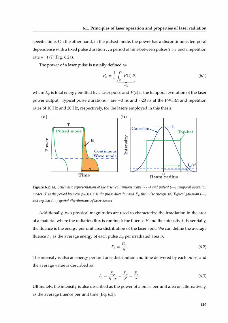
6.1. Principles of laser operation and properties of laser radiation
specific time. On the other hand, in the pulsed mode, the power has a discontinuous temporal
dependence with a fixed pulse duration τ, a period of time between pulses T>τand a repetition
rate ν=1/T (Fig. 6.2a).
The power of a laser pulse is usually defined as
Pp =1
τ
∫ τ
0P (t)dt︸ ︷︷ ︸Ep
, (6.1)
where Ep is total energy emitted by a laser pulse and P (t) is the temporal evolution of the laser
power output. Typical pulse durations τ are ∼3 ns and ∼20 ns at the FWHM and repetition
rates of 10 Hz and 20 Hz, respectively, for the lasers employed in this thesis.
Time
Pow
er
ContinuousWave mode
Pulsed mode
Beam radius
Inte
nsity
0
I0
I0/e2
Top-hatGaussian
T
τ
Ep
(a) (b)
Figure 6.2: (a) Schematic representation of the laser continuous wave (- - -) and pulsed (—) temporal operation
modes. T is the period between pulses, τ is the pulse duration and Ep the pulse energy. (b) Typical gaussian (—)
and top-hat (—) spatial distributions of laser beams.
Additionally, two physical magnitudes are used to characterize the irradiation in the area
of a material where the radiation flux is confined: the fluence F and the intensity I . Essentially,
the fluence is the energy per unit area distribution of the laser spot. We can define the average
fluence Fp as the average energy of each pulse Ep per irradiated area S,
Fp =EpS. (6.2)
The intensity is also an energy per unit area distribution and time delivered by each pulse, and
the average value is described as
Ip =EpS · τ
=PpS
=Fpτ. (6.3)
Ultimately, the intensity is also described as the power of a pulse per unit area or, alternatively,
as the average fluence per unit time (Eq. 6.3).
149

6. Fundamental aspects of laser processing of materials
Typically, the beam cross-section can present different spatial profiles denoted as
transverse electromagnetic modes (TEM). Most laser beams employed for material processing
present a Gaussian or nearly-Gaussian spatial distribution which corresponds to the
fundamental mode (TEM00). This distribution is characterized by a maximum of intensity I0
at r=0 and a characteristic radius w defined as the value when I=I0=e2 (Fig. 6.2b). The top-hat
spatial distribution illustrated in Fig. 6.2b is often required in laser processing when a uniform
irradiation is mandatory. This shape is obtained by modulating the laser beam using an
homogenizing device albeit having associated a loss in the energy output. Despite some
applications may use higher-order modes, they are generally blocked in the laser cavity.
Additional information of temporal and spatial distributions can be found elsewhere
[125, 254, 255]. A description of the particularities of the experimental setup used in this thesis
can be found in section 2.3.3.
6.2 Laser-matter interactions in the processing of materials
The electromagnetic radiation interacts with a material through the absorption, reflection,
refraction, scattering or transmission of the incident light (Fig. 6.3). Among these processes,
absorption is the most important effect in laser processing of materials, and it may result in
diverse and complex phenomena leading to material modification (doping, alloying,
oxidation, reduction, nitridation, exchange of surface atoms/molecules), decomposition,
polymerization, heating, melting, material vaporization, etc. The extent of these effects will
generally depend on the characteristics of laser radiation (intensity, wavelength, spatial
distribution, temporal evolution, angle of incidence, polarization, irradiation time,...), and the
chemical and thermo-physical properties of the material (optical absorption, thermal
conductivity, specific heat, density, latent heats,...).
A material response to the electromagnetic radiation is characterized by the complex
refractive index N=niη, being n the refractive index and η the extinction coefficient. Notice
that both parameters depend on the wavelength of the radiation. When the incident laser
intensity I0 reaches the surface of a material part of the incoming radiation will be reflected Ir.
We can define the reflectance R at normal incidence as
R =IrI0
=
N 1
N + 1
2 =(n 1)2 + η2
(n+ 1)2 + η2: (6.4)
The remaining radiation will be absorbed and transmitted through the material. This effect is
150

6.2. Laser-matter interactions in the processing of materials
Reflectedbeam
Material
Incidentbeam, I0
Transmittedbeam, It
Scattered beam
Figure 6.3: Schematic representation of the possible mechanisms caused by interactions between laser radiation
and matter. Reproduced from [255].
usually described in terms of the Lambert-Beer law as
I(z) = I0(1R) exp (z) ; (6.5)
where I0 and I(z) are the intensity of incidence and at a depth z, respectively. The absorption
coefficient is defined by
=4βη
λ: (6.6)
Thus, the intensity of the radiation decreases exponentially inside the material. The optical
penetration depth (l=1=) is a common parameter used for the evaluation of light
absorption, indicating at which depth the attenuation has a value of I0=e. Typically, η depends
on the wavelength of the radiation and temperature, thus, will also be a function of these
parameters.
6.2.1 Photothermal and photochemical processes
The electromagnetic radiation emitted by lasers is absorbed by the electrons present in the
irradiated material causing a transition to a higher energy state. The excited electrons will
provoke different effects which can be generally divided in photothermal (heating, melting,
vaporization,...) or photochemical processes (activation of chemical reactions, plasma
formation, ...). These diverse phenomena, which are classified depending on the interaction
time and the intensity of the laser radiation, are summarized in Fig. 6.4.
Typically, the thermalization of the excitation produced in a material after irradiation is
caused by the electron-phonon coupling and takes place in times of the order of
θT〈10121010 s. Therefore, we will say that a process is (photo-)thermally activated if it
151
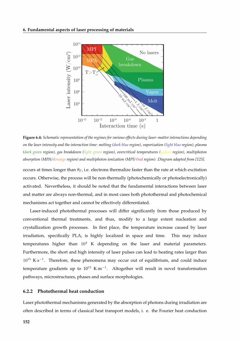
6. Fundamental aspects of laser processing of materials
10 mJ/cm2
100 mJ/cm2
1 J/cm2
10 J/cm2
No lasersGas
breakdown
Plasma
Vapor
Melt
MPI
MPA
T>Tcr
Lase
r in
tens
ity (
W/c
m2 )
Interaction time (s)
104
106
108
1010
1012
1014
10-15 10-12 10-9 10-6 10-3 1
Figure 6.4: Schematic representation of the regimes for various effects during laser–matter interactions depending
on the laser intensity and the interaction time: melting (dark blue region), vaporization (light blue region), plasma
(dark green region), gas breakdown (light green region), overcritical temperatures (yellow region), multiphoton
absorption (MPA) (orange region) and multiphoton ionization (MPI) (red region). Diagram adapted from [125].
occurs at times longer than θT , i.e. electrons thermalize faster than the rate at which excitation
occurs. Otherwise, the process will be non-thermally (photochemically or photoelectronically)
activated. Nevertheless, it should be noted that the fundamental interactions between laser
and matter are always non-thermal, and in most cases both photothermal and photochemical
mechanisms act together and cannot be effectively differentiated.
Laser-induced photothermal processes will differ significantly from those produced by
conventional thermal treatments, and thus, modify to a large extent nucleation and
crystallization growth processes. In first place, the temperature increase caused by laser
irradiation, specifically PLA, is highly localized in space and time. This may induce
temperatures higher than 104 K depending on the laser and material parameters.
Furthermore, the short and high intensity of laser pulses can lead to heating rates larger than
1015 Ks1. Therefore, these phenomena may occur out of equilibrium, and could induce
temperature gradients up to 1015 Km1. Altogether will result in novel transformation
pathways, microstructures, phases and surface morphologies.
6.2.2 Photothermal heat conduction
Laser photothermal mechanisms generated by the absorption of photons during irradiation are
often described in terms of classical heat transport models, i. e. the Fourier heat conduction
152

6.2. Laser-matter interactions in the processing of materials
equation, due to their simplicity. In order to do so, it must be assumed that the system is in a
local thermodynamic equilibrium. This only happens when the diffusion time of the system is
much longer than the relaxation times for energy transfer, and when the characteristic length is
much larger than the mean free path. Typically, relaxation times are in the picoseconds range
which allow fairly precise modeling of heat transfer in nanosecond or longer-duration pulsed-
laser heating of materials.
The general form of the heat equation can be written as
αCp@T
@t∇ [kth∇T ] = Q; (6.7)
where α, Cp, kth and T are the density, specific heat at constant pressure, thermal conductivity
and temperature, respectively. Although these parameters are generally temperature
dependent, they are often considered constant in first approximation for the sake of simplicity
and due to the difficulty to find reliable data in a wide range of temperatures. Q in Wm3 is
the volumetric energy intensity absorbed, usually seen as the heat source of the radiation.
If the radiation absorbed in our material is completely converted into heat,Q can be written
as
Q = G(t)P (x; y)(1R) exp (z) ; (6.8)
where G(t) is the temporal dependence of the laser pulse, P (x; y) is the spatial distribution of
incident intensity on the surface of our material,R is the surface reflectance at normal incidence
(Eq. 6.4), is the absorption coefficient (Eq. 6.6) and z is the depth. In our particular case,
despite having non-uniform beam shapes, i. e. gaussian for the Nd:YAG laser and only top-
hat along one direction for the excimer laser, the spatial shape of our beam will be taken to
be constant for simplicity and P (x; y)=F=θ . The temporal dependence of the laser pulse will
be assumed to follow a gaussian distribution of the form G(t)=exph4 ln(2) (t θ)2 =θ2
isince
θ is defined at the FWHM. Additional information of pulse and beam shapes can be found
elsewhere [125].
The thermal-diffusion length is a parameter commonly employed to evaluate heat
propagation inside a material during a time θ and is given by
lth =
sZ
0D(T (t))dt = 2
pDthθ ; (6.9)
where Dth=kth=αCp is the thermal diffusivity.
Finally, it must be noted that the diffusion of the thermal front after absorption (Fig. 6.5a)
may lead to various phenomena:
153

6. Fundamental aspects of laser processing of materials
• The solid-state recrystallization of the material may occur when the temperature reached
inside the material is below the melting point Tmp (Fig. 6.5b).
• Temperatures higher than Tmp will lead to a phase transition into a molten state of the
previously solid material (Fig. 6.5c). Once irradiation is over, the material will resolidify.
The final composition and microstructure highly depend on the cooling rate.
• Vaporization can occur at the materials’ surface when the intensity of the laser radiation is
high enough (Fig. 6.5d). In this case, vapor entities may also absorb part of the radiation
which would lead to the formation of a plasma plume.
Additional information about the different effects induced by laser irradiation can be found
elsewhere [125].
Absorption
Laser beam
Sample
Heat conduction
Heat affectedzone
(a) (b)
Melting(c)Moltenmaterial
Heatfront
Sample
Sample
Vaporization/Plasma formation
Vapor
(d)
Sample
Plasma
Figure 6.5: Schematic representation of the (a) absorption of laser radiation, and induced (b) heating, (c) melting
and (d) vaporization/plasma formation.
6.3 Modeling the photothermal effect of pulsed laser annealing for
thin film processing
Although photo-induced crystallization could present a photochemical contribution due to the
high energetic photons, it is usually analyzed in terms of photothermal processes. This is so
because the excitation is performed at longer times than thermalization of the electrons [125],
i. e. the pulse width of the lasers used is in the range of nanoseconds.
If a quantitative analysis and optimization of a particular process is wanted, the
154

6.3. Modeling the photothermal effect of pulsed laser annealing for thin film processing
laser-induced temperature distribution in a system must be known. However, direct
measurements of temperature are often complex due to its fast evolution in a material which
is caused by the pulsed nature of the radiation. Thus, modeling is a common tool to extract
quite accurate temperature distributions.
In this section, we will present the equations employed to simulate photothermal
processes caused by laser-matter interactions, as well as the assumptions and limitations of
the model used. In addition, we will particularize simulations for our oxide heterostructures
by describing the influence of different parameters on thermal distributions and the
information we can obtain from simulations. These models were implemented using the
COMSOL multiphysics 4.4 software. Finally, we will describe the technical aspects involved in
the simulation process. In the next chapters, we will make use of these simulations to support
the experimental data on laser decomposition (Chapter 7) and crystallization (Chapter 8) and
guide the experiments undertaken.
6.3.1 Technical aspects, model implementation and limits of validity of
temperature simulations
Many physical phenomena are usually described in terms of differential equations such as
the heat equation. Solving these equations analytically is often complex or even impossible.
Thus, numerical techniques such as the finite element method (FEM) arise as a vital tool for
the systematic and simple resolution of any set of equations. In addition, calculations can be
done in any desired geometry and allow the introduction and modification of a broad range of
parameters.
Basically, the application of FEM consists of dividing a geometry in small domains and
solve a set of differential equations in each domain. Then, it is necessary to define the initial
and boundary conditions, discretize the equations through meshing and interpolate. Finally, it
involves the acquisition and interpretation of results, and error analysis. Regardless, it must be
noted that numerical calculations do not provide a general relationships and they are always
limited to finite regions. Furthermore, inappropriate discretizations of the problem can cause
artifacts. Additional information about numerical techniques can be found in the literature
[256, 257].
In our case, the simplest analysis of the temperature distribution is based on the
one-dimensional solution of the heat conduction equation (Eq. 6.7). To do so, we assumed
that there is symmetry along the XY plane and that the thermal diffusion length during a
155

6. Fundamental aspects of laser processing of materials
single pulse is significantly smaller than the laser spot (hundreds of nanometers compared to
millimeters). In the numerical simulations the material is considered homogeneous and its
thermo-physical properties independent of temperature, the initial temperature of the
material T0 is constant, the heat input is uniform during irradiation, and convection and
radiation losses are negligible, i. e. the system is adiabatic.
The modeling of temperature distributions has been done assuming a general set of layers
as illustrated in Fig. 6.6a. The general source term from Eq. 6.8 can be written for an arbitrary
layer Ln as
Qn =F
θexp
"4 ln(2)
(t θ)2
θ2
#
(1Rn)n exp
"n
z
n1Xi=1
Li
!#24n1Yj=1
(1Rj) exp (jLj)
35 : (6.10)
Usually, we considered film/substrate or film/buffer layer/substrate architectures because of
the heterostructures investigated.
The in-plane size has been chosen to be of 100 nm to minimize the calculation time (Fig.
6.6b). For the spatial discretization of our system, we used triangular meshes with a maximum
size for each unit two orders of magnitude smaller than the optical penetration depth (l) and
minimum sizes of 0.1 nm. Moreover, we increased the mesh density around interfaces to obtain
smooth transitions between materials. For the temporal discretization, we employed steps of
0.5 ns from 0 to 10 ns, 1 ns from 10 to 20 ns, 5 ns from 20 to 50 ns, 10 ns from 50 to 100 ns, and
100 ns from 100 to 1000 ns.
Substrate
Buffer layer
Film0
z
L1
L2
Ln
(a) (b) 0
20
40
60
80
1000 20 40 60 80 100
Width (nm)
Dep
th (
nm)
Figure 6.6: (a) Schematic representation of the general layer system considered. (b) Example of the meshing
used in temperature simulations for a layer/substrate architecture. Equivalent mesh precision is employed when
additional layers are present.
156

6.3. Modeling the photothermal effect of pulsed laser annealing for thin film processing
Resolution of the system of equations was done using the Parallel Direct Sparse Solver
Interface (PARDISO) and a nested dissection multithreaded row preordering algorithm with an
automatic scheduling method. The numerical error of simulations has been evaluated through
the convergence of the solution, and thus, the results described have a minimum uncertainty
due to the numerical approximations of our model described next.
Despite the heat equation illustrates easily temperature distributions in most laser
processing situations, there are some constrains and uncertainties to be aware of [125]:
• Thermal fluctuations are assumed to be small even though we are dealing with structures
in the submicrometer range.
• The thermo-physical and optical properties of materials, i. e. , R, kth, Dth, Cp, etc, are
frequently extracted from measurements without large temperature gradients.
However, these gradients (rT→T=l) achieved during laser annealing may be rather
intense (〈1051015 Km1) with extremely short interaction times. Under these
circumstances, the exact values for the aforementioned parameters may be very distinct
compared to their conventional thermal treatment counterparts.
• Usually, the temperature dependence of the thermo-physical and optical parameters is
only known in a small interval of temperatures. However, a wide range of temperatures
is achieved with lasers, i. e. from tens to thousands of ºC.
• These physical properties highly depend on surface morphology, crystallinity, surface
contaminants, defects, etc.
• In addition, the material is modified with each pulse sent, and thus, its physical properties
will change continuously.
• The contribution of internal reflections to heating has been simulated and it is negligible
compared with the contribution of other parameters.
• Feedback reactions are common in laser-matter interactions due to coupling between
different phenomena. This would require considering coupled non-linear equations in
their theoretical description.
In summary, measurement of the relevant quantities during laser processing and inclusion of
the multiple phenomena in the model would be the best solution to some of these limitations.
Regardless, we will demonstrate that quite accurate modeling of temperature distributions can
be obtained and this will be fundamental to guide and interpret the laser processing results in
the following chapters.
157
6. Fundamental aspects of laser processing of materials
6.3.2 Different contributions to the overall thermal behavior
Considering the constrains of the model presented in the previous section, we will now
particularize to our experiments by giving a general description of the information that can be
extracted and the influence of the different optical, thermo-physical and processing
parameters, mainly the fluence and substrate base temperature, in the resulting temperature
distributions.
Once a laser pulse reaches a material, the surface temperature will rise extremely fast and
the heat will diffuse towards the substrate. As we mentioned previously, heat diffusion will
depend on the thermo-physical properties of each material. Cooling will start right after and
temperature will decrease very rapidly. Fig. 6.7 shows the heating/cooling and the heat
transfer process through a CZO/YSZ heterostructure for a fluence of 40 mJcm2, the
substrate at room temperature and a laser with a pulse duration of 3 ns. In Fig. 6.8a, we can
see the temporal dependence of temperature for the process described in Fig. 6.7. The
maximum temperature in the system is reached only 1 ns after the laser pulse ends (θ〈3 ns).
Afterwards, the system will start cooling down. It is important to notice that the time needed
to cool the system down to temperatures close to the initial value is significantly longer than
time required for heating, i. e. few nanoseconds as compared to tens or hundreds of
nanoseconds (Fig. 6.8a).
Modeling of temperature distributions allows us to obtain several vital parameters that will
help to understand the growth of oxide heterostructures:
• The maximum temperature Tmax reached in a system can be extracted from the time
dependence of the temperature profile (Fig. 6.8a). This allow us to select an appropriate
working range of fluences that match with the temperatures we want. Furthermore, we
can distinguish between surface and interface temperature profiles which provide the
temperature gradient inside the oxide film.
• The effective heating time teff is a reference for the effective duration of the laser
treatment and can be defined as the amount of time above a certain arbitrary
temperature. In this work, we have considered that 600 ºC should be the threshold
temperature for crystallization since we assume that diffusion is slow below that value
in solid-solid processes (Fig. 6.8b).
• Temperature distribution along thickness of our heterostructure for a given time can be
extracted as well (Fig. 6.8c). This provides information about the temperature
158

6.3. Modeling the photothermal effect of pulsed laser annealing for thin film processing
0 ns 1 ns 3 ns 4 ns
10 ns 50 ns
1500 ºC
1250 ºC
1000 ºC
750 ºC
500 ºC
250 ºC
Film
Substrate
Hea
ting
Coo
ling
5 ns 7 ns
Figure 6.7: Color evolution of temperature inside a CZO/YSZ heterostructure. Simulations were done for a
fluence of 40 mJcm2 and the substrate at room temperature.
distribution through thickness, for example, between the surface and multiple
interfaces, and the temperature gradient along the whole heterostructure.
The influence of these parameters on the heterostructures investigated will be discussed in the
following sections and chapters.
Many variables may contribute to the temperature profile in a film during laser irradiation
and, therefore, influence decomposition and crystallization. On the one hand, thermo-physical
and optical parameters have a large repercussion on heating. Table 6.1 presents the main optical
and thermo-physical properties for the materials considered in this thesis. It should be noted
that the absorption coefficient will be the materials physical property having a larger influence
in our simulations and the remaining parameters will affect on the heat transfer through the
heterostructure. For instance, thermal diffusion will be promoted when thermal conductivity
is high. However, the specific heat capacity, i. e. the energy required for the system to increase
its temperature 1 ºC, must be small. Additionally, the denser a material the worse is the heat
transfer. Despite all these values are temperature dependent, all quantities presented have been
measured at 300 K due to the lack of data covering a wide range of temperatures. These values
have been obtained from the literature or experimental measurements as indicated in Table 6.1.
159

6. Fundamental aspects of laser processing of materials
Table6.1:
Thermophysicaland
opticalparameters
forthe
differentoxides
investigated:opticalabsorption
coefficient(
)and
penetrationdepth
(lα ),reflectance(R
),
density(α),therm
alconductivity
(kth ),specific
heatcapacity
atconstant
pressure(Cp ),and
melting
point(Tmp ).
yand
xindicate
thatw
eobtained
thedata
from
spectrophotometry
andellipsom
etry,respectively.M
easurements
havebeen
doneatroom
temperature
(300K
).Theopticalparam
etersare
fora
wavelength
of266nm
,
exceptforthe
onesindicated
at248nm
.Rem
ainingparam
eterscan
befound
inR
efs.[122,125,196,246,258–278].
Material
α(1
06
m1)
lα=α1
(nm)
Rρ
(g·cm3)
kth
(W·m1·K1)
Cp
(J·kg1·K1)
Tmp
(ºC)
Ce/Z
rpropionate
4.0y
2500.02
y1.8
(s)/1.5(l)
0.6(s)/0.3
(l)1786
(s)/2110
(l)235
CZ
O31.0
y32
0.10y
7.22.6
3532400
LNO
12.6y/21.2
(cryst.)79/48
(cryst.)0.15
y7.2
10400
168023.6
(cryst.,@248
nm)
42(cryst.,@
248nm
)
BST20.9
y48
0.07y
5.94.1
4721625
28.1y
(@248
nm)
36(@
248nm
)
LSMO
24.1y
420.05
y5.9
2.5530
1450
YSZ
(SC)
0.4x
25000.18
x5.7
2446
2988
YSZ
(ABA
D)
1.2x
8000.13
x5.7
2446
2988
SS82.0
x12
0.41x
814.3
4591455
STO60.0
170.20
5.18.3
5451910
LAO
0.005200000
0.016.5
11.7448
2100
Pt10.5
(@248
nm)
10(@
248nm
)0.50
21.572
1331770
SiO2
--
-2.2
1.6740
1600
Si-
--
2.3152
7001420
160

6.3. Modeling the photothermal effect of pulsed laser annealing for thin film processing
(a) (b)
0
500
1000
1500
0.1 1 10 100 1000
Tem
pera
ture
(ºC
)
Time (ns)
Laser pulse(τ∼3 ns)
InterfaceSurface
Tmax
Laser intensity (a.u.) 0
500
1000
1500
0.1 1 10 100 1000
Tem
pera
ture
(ºC
)
Time (ns)
teff600 ºC
1 10 100 1000 10000
Depth (nm)
0
500
1000
1500
Tem
pera
ture
(ºC
)
Inte
rfac
e
CZO YSZ
(c)
Figure 6.8: (a) Surface (—) and interface (—) time dependence of the temperature for a 20 nm-thick CZO
film on a YSZ substrate. The maximum temperature and laser pulse (- - -) have been represented for better
comprehension. Despite the laser intensity axis will not be indicated in the next plots, the laser pulse will be kept
for comparison purposes. (b) Effective heating time determination from time-dependent temperature profiles. (c)
Simulated temperature distribution along samples depth. Simulations were done for a fluence of 40 mJcm2 and
the substrate at room temperature.
6.3.2.1 Influence of laser fluence and pulse duration on temperature distributions
The laser output is the first and most important factor that will determine the temperature
distribution in our sample. In first place, we have the fluence F which is the energy per unit
area arriving to the surface of our sample, which has been assumed constant along the whole
surface in our simulations. Fig. 6.9a shows the dependence of the temperature profiles with
fluence for a 20 nm-thick CZO film on YSZ. It can be seen that the temperature evolution at the
sample’s surface and its maximum value increase linearly with the fluence (Fig. 6.9b). In turn,
this leads to a non-linear rise in the effective heating time (Fig. 6.9c).
The duration of the laser pulse is also another important parameter. For instance, we
evaluated what would happen if we increase the pulse duration of the Nd:YAG laser (θ〈3 ns)
to that of the excimer laser (θ〈25 ns) for a fixed fluence of 40 mJcm2 and without modifying
any other parameter. In this case, Fig. 6.9d reveals that longer laser pulses derive in
161

6. Fundamental aspects of laser processing of materials
(a)
(c)
0500
10001500200025003000
Tem
pera
ture
(ºC
)
0.1 1 10 100 1000Time (ns)
80 mJ·cm-2
60 mJ·cm-2
40 mJ·cm-2
20 mJ·cm-2
0
500
1000
1500
Tem
pera
ture
(ºC
)
0.1 1 10 100 1000Time (ns)
Laser pulse(τ∼3 ns)
Temp. profile(τ∼3 ns)
Laserpulse
(τ∼25 ns)Temp. profile
(τ∼25 ns)
(d)
(b)
20 40 60 80500
1000
1500
2000
2500
3000
Max
. tem
p. (
ºC)
Fluence (mJ·cm-2)
20 40 60 8010
20
30
40
Effe
ctiv
e he
atin
gtim
e, t e
ff (n
s)
Fluence (mJ·cm-2)
Figure 6.9: (a) Sample's surface temperature evolution with time for a 20 nm-thick CZO films on YSZ substrates
at room temperature for fluences of 20 mJcm2 (—), 40 mJcm2 (—), 60 mJcm2 (—) and 80 mJcm2 (—). (b)
Maximum temperature and (c) effective heating time dependence with the laser fluence. (d) Temperature profiles
for laser pulse durations of 3 ns (—) and 25 ns (—) at a fluence of 40 mJcm2. Parameters used in the simulations
are summarized in Table 6.1. The laser pulses, i. e. 3 ns (- - -) and 25 ns (- - -) are plotted for comparison.
temperature profiles with lower temperatures which is caused by a reduction in the input
power (P=F=θ ) due to the higher pulse duration (θ〈25 ns). Consequently, higher fluences
will be needed to achieve an effect similar to the one obtained at 3 ns. Notice that maximum
peak temperatures thousand degrees apart may be reached in this particular case, leading to a
significant reduction of the effective heating time for θ〈25 ns.
6.3.2.2 Influence of substrate/buffer layer absorption and substrate temperature
The contribution of substrates may be vital to crystallization of oxide heterostructures. This is
especially critical for films with thicknesses smaller than the optical penetration depth
(l=1), i. e. small absorption coefficients. Typically, the oxide films investigated (CZO,
LNO, BST and LSMO) have thicknesses between 20 and 40 nm after decomposition, whereas
the corresponding l values are larger at the working laser wavelength (Tables 5.1 and 6.1).
162

6.3. Modeling the photothermal effect of pulsed laser annealing for thin film processing
From the Lambert-Beer law (Eq. 6.5), this implies that films will absorb only part of the
incoming radiation and, therefore, substrate absorption and corresponding heating process
will be very important for film crystallization.
Fig. 6.10a shows the transmittance data from spectrophotometry measurements described
in section A.4.2. We can see that transmittance of LAO is larger than YSZ and STO at the laser
wavelengths employed, i. e. 248 and 266 nm. Thus, we expect a higher absorption of the
laser radiation in STO, and a subsequent enhancement of heating and crystallization for films
deposited on STO.
Temperature simulations of a 10 nm-thick BST film on LAO, LNO-buffered LAO and STO
substrates (Fig. 6.10b) illustrate the influence of substrate absorption. A fluence of 40 mJcm2,
a substrate temperature of 400 ºC and a pulse duration of 3 ns were considered. Parameters
employed for the calculations are summarized in Table 6.1. On the one hand, the maximum
temperatures reached in the BST/STO (〈1300 ºC) heterostructures are respectively 500 and
700 ºC higher than those in BST/LNO/LAO (〈800 ºC) and BST/LAO (〈600 ºC). On the other
hand, the effective heating time is around 26 ns for BST/STO and 6 ns for BST/LNO/LAO,
while teff 〈 0 ns for BST/LAO because this system does not reach 600 ºC. Consequently, the
importance of substrate and buffer layer absorption may have to promote crystallization of the
oxide film is crucial.
In addition, base temperature of substrates is also critical since it contributes to an overall
temperature rise in the heterostructure. In Fig. 6.11a, we plot the temperature profiles for a 20
nm-thick CZO film on YSZ for a fluence of 40 mJcm2 and the substrate at room temperature,
200 250 300 350 400 450 5000
20406080
100
Tran
smita
nce
(a.u
.)
Wavelength (nm)
STO
LAO
YSZ
266248
0.1 1 10 100 1000400
600
800
1000
1200
1400
Tem
pera
ture
(ºC
)
Time (ns)
BST (10 nm)on LAO
BST (10 nm)on STO
BST (10 nm)on LNO/LAO
(a) (b)
Figure 6.10: (a) Comparison of the transmittance for LAO, YSZ and STO substrates. (b) Temperature simulations
of a 10 nm-thick BST film on LAO (—), LNO/LAO (—) and STO (—) using a fluence of 40 mJcm2 and a
substrate temperature of 400 ºC. The solid lines (—) and dashed (- - -) lines indicate the surface and interface
temperature evolution, respectively. Parameters used in the simulations are summarized in Table 6.1.
163

6. Fundamental aspects of laser processing of materials
200 ºC and 400 ºC. It can be seen from Fig. 6.11b that the maximum temperature rises linearly
with the substrate temperature and this leads to a non-linear increase of the effective heating
time (Fig. 6.11c)
(a) (b)
0
400
800
1200
1600
2000
0.1 1 10 100 1000
Tem
pera
ture
(ºC
)
Time (ns)
400 ºCLaser pulse(τ∼3 ns)
200 ºCRoomTemp.
(c)
RT 200 4001400
1500
1600
1700
1800
1900
Max
. tem
p. (º
C)Substrate temperature (ºC)
RT 200 4000
20
40
60
80
Effe
ctiv
e he
atin
gtim
e, t
eff (
ns)
Substrate temperature (ºC)
Figure 6.11: (a) Temperature profiles of 20 nm-thick CZO films on YSZ substrates. A fluence of 40 mJcm2
and the substrate at room temperature (—), 200 ºC (—) and 400 ºC (—) were used. The laser pulse (- - -) has
been plotted for comparison. (b) Maximum temperature and (c) effective heating time dependence with substrate
temperature extracted from the temperature profiles as explained in section 6.3.2.
Altogether indicates that substrates have a critical role determining the experimental
conditions in laser processing which differs from those of conventional (iso-)thermal
treatments.
6.3.2.3 Influence of the oxide film thickness on temperature distributions
The film thickness L will also have a large influence over temperature profiles. If L is smaller
than the optical penetration depth l, substrates will have a larger contribution to heating as
compared to their influence if L>l. We will describe these differences using the case of
BST/LAO heterostructure since in this particular example this effect is very relevant.
Figs. 6.12a and b illustrate, respectively, the temperature dependence with time for 10, 50
164

6.3. Modeling the photothermal effect of pulsed laser annealing for thin film processing
and 160 nm-thick BST films on LAO, and the behavior of surface and interface peak
temperatures with the film thickness for a fluence of 40 mJcm2 and a substrate temperature
of 400 ºC. On the one hand, surface peak temperature increases with film thickness and it
seems to saturate around 1400 ºC. On the other hand, interface peak temperature rises until
film thickness is equivalent to the optical penetration depth and it decreases for L>l. Finally,
surface effective heating times increase with film thickness, whereas the teff at the interface
rises until L〈100 nm and, then, decreases (Fig. 6.12c).
Several reasons may lead to the phenomena described though it must be noted that this
description will highly depend on the heterostructure and its physical parameters. Firstly,
surface and interface temperatures and effective heating times increase when L<l because
LAO is very small compared to BST (Table 6.1). Consequently, more radiation is being
0.1 1 10 100 1000400600800
100012001400
Tem
pera
ture
(ºC
)
Time (ns)
10 nm
160 nm
SurfaceInterface
Interface
Surface
50 nmInterface
Surface
(a) (b)
(c)
0 40 80 120 160400600800
100012001400
Tem
pera
ture
(ºC
)
Thickness (nm)
1600
Surface
Interface
Opticalabsorptionlength
0 40 80 120 1600
10
20
30
40
Effe
ctiv
e he
atin
gtim
e, t e
ff (n
s)
Thickness (nm)
Surface
Interface
Figure 6.12: (a) Surface (—) and interface (- - -) temperature profiles of BST films on LAO for thicknesses of 10
nm (black), 50 nm (blue) and 160 nm (red). Surface (black up triangles) and interface (red down triangles) (b) peak
temperature and (c) effective heating time dependence with film thickness. A fluence of 40 mJcm2 and a substrate
temperature of 400 ºC were used for the simulations. Thermo-physical and optical properties are summarized in
Table 6.1.
165
6. Fundamental aspects of laser processing of materials
absorbed by the film as it becomes thicker, contributing to its heating. When L>l, the
limiting factor is not the absorption coefficient but the thermo-physical properties of the
system characterized by the thermal-diffusion length lth (Eq. 6.9), i.e. 〈130 nm at 300 K for
BST, because all the radiation is being absorbed inside the film.
6.4 Summary and conclusions
In this chapter, we have discussed the basic concepts involved in the laser processing of
materials.
Firstly, we described the mechanism of operation of lasers, i.e. how the laser beam is
generated through population inversion by pumping electrons to higher electronic states,
stimulated emission of photons and amplification of the effect; as well as the properties of the
radiation emitted (monochromaticity, collimation and coherence), and the spatial and
temporal characteristics of the resulting laser radiation.
In second place, we detailed the interaction of the laser radiation with materials through
the absorption of photons and the multiple phenomena derived, generally classified as
photothermal and photochemical processes.
Finally, we introduced the numerical model employed for the evaluation of
photothermally-induced heating. Particularly, we presented the heat conduction and source
term equations employed in simulations. In addition, we also discussed about the
assumptions taken and limitations of the model, as well as the influence of optical,
thermo-physical and experimental parameters such as fluence, substrate temperature or film
thickness in the final temperature distributions. We can conclude that numerical simulations
are an excellent tool that has allowed us to guide the experiments of this thesis and give more
insight into the mechanisms governing decomposition and crystallization of CSD precursor
films.
166
Chapter 7
Laser decomposition of metal-organic
Ce0.9Zr0.1O2y precursor films
Chemical solution deposition (CSD) has been used widely for the low-cost production of
ceria-based materials [11, 21, 55, 190]. Thermal treatments, i. e. conventional or rapid thermal
annealing (CTA or RTA), are typically used for the decomposition of precursor films and
oxide phase crystallization. However, they involve thermodynamic equilibrium and rather
long processing times, limiting versatility for the fabrication of devices.
It is known that lasers are energy sources with a fast pulsed nature and allow to process
materials with large spatial resolution (Chapter 6). This makes them very appealing for the
decomposition and crystallization of metal-organic films, and production of functional
devices [72, 279, and references therein]. As we mentioned before, complex phenomena such
as photochemical reactions, heating, melting, ultra-fast crystallization, etc, occur when laser
radiation is absorbed inside a material [70, 125, 280]. Specifically, decomposition of organic
materials caused by extremely fast (ps-ns) photochemical and/or thermal mechanisms in
conditions commonly far-off the thermodynamic equilibrium is used for many different
purposes such as lithography, polymer micro-machining, or laser direct writing of conductive
metallic films on plastic substrates [281–283, and references therein].
In this chapter, we will investigate the decomposition by laser irradiation of metal-organic
(Ce, Zr)-propionate thin films on (001) YSZ substrates which are often employed for the
growth of CZO epitaxial films. In particular, we will describe the morphology and properties
of propionate films prior to laser irradiation. Then, we will evaluate the optimization of laser
processing conditions and discuss the effect of parameters such as fluence, number of pulses
167

7. Laser decomposition of metal-organic Ce0:9Zr0:1O2y precursor films
and substrate temperature on films morphology and composition. Further crystallization of
metal-organic films by CTA will be analyzed as well. Finally, we will validate the use of laser
processing for the design and fabrication of micrometric patterns. Notice that all the
experiments in this chapter involving laser decomposition have been done using a Nd:YAG
laser working at 266 nm in air (section 2.3.3).
7.1 State of metal-organic films before decomposition
The AFM characterization of Ce-Zr propionate films deposited on YSZ by spin-coating and
dried with a hot-plate at 90 ºC for 10 min (Figs. 7.1a and b) shows that they have extremely
flat surfaces with roughness around 0.5 nm, despite there are some small holes present. In
addition, the thickness measured by removing one part of the metal-organic film is around 80
nm (Fig. 7.1c).
1 µmRMS=0.6 nm 5 µm
(c)
0 5 10 15 20
Hei
gtht
(nm
)
Length (µm)
020406080
(a) (b)
Figure 7.1: AFM image of a metal-organic CZO precursor film. (a) 5 x 5 νm2 scan illustrating film's surface,
and (b) 20 x 20 νm2 scan with a step employed to determine film thickness. (c) Line scan of (b) illustrating films
thickness.
We have also measured the optical properties, i. e. transmittance and reflectance (Fig.
7.2a), before irradiation by spectrophotometry as explained in Appendix A.4.2. The precursor
film was deposited on a (0001)-oriented alumina (-Al2O3) substrate using the experimental
conditions described in section 2.2. Alumina substrates where chosen due to its transparency
in a wide spectral range. In addition, we derived important parameters such as the refractive
index n, extinction coefficient η, optical absorption coefficient and penetration depth l
(Figs. 7.2b and c). Specifically, n and η were determined using the Denton method [284] as
described in section A.4.2.
Fig. 7.2b shows that n and η present local maximum values at 280, 700 and 870 nm, the
largest corresponds to that near 266 nm , i. e. the Nd:YAG laser wavelength. Furthermore, the
n and η range from 1.83 to 1.91, and from 0.04 to 0.10 for wavelengths between 200 and 1100
168

7.2. Optimization of irradiation conditions for the decomposition of CZO precursor films
(a) (b)
020406080
100
%
200 400 600 800 1000Wavelength (nm)
Transmittance
Reflectance0.0
0.1
1.8
1.9
2.0Refractive index, n
Extinction coefficient, κ
200 400 600 800 1000Wavelength (nm)
200 400 600 800 10000
1
2
153045
α(1
05 m-1)
Wavelength (nm)
l α(1
02 nm
)
(c)
Figure 7.2: Dependence of the optical properties of Ce-Zr metal-organic films with wavelength: (a) transmittance
and reflectance, (b) refraction index n and extinction coefficient η, and (c) optical absorption coefficient and
penetration depth lα.
nm, respectively. In Fig. 7.2c, we can see that diminishes as the wavelength increases and
also presents a maximum at 280 nm. Its value at 266 nm is 〈4106 m1 which gives a value of
l〈250 nm, i. e. larger than the precursor film thickness (Fig. 7.1b). If we apply the Lambert-
Beer formula (Eq. 6.5) using the aforementioned values, we can see that only a 27% of the laser
light is being absorbed by the precursor film. Consequently, the remaining radiation will arrive
to the substrate.
The thermal energy inside the substrate contributing to the decomposition of the Ce-Zr
precursor film will essentially depend on its optical and thermophysical properties (Table 6.1).
This fact provides to the substrate a role in laser processing that does not exist in conventional
annealing as mentioned in section 6.3.2. Since YSZ has a Y SZ〈4105 m1 and a thickness
〈0.5 mm, all the radiation will be absorbed in it leading to its heating, and thus, affecting
decomposition of the Ce-Zr propionates.
7.2 Optimization of irradiation conditions for the decomposition of
CZO precursor films
Ce-Zr propionate metal-organic films on YSZ have been irradiated by laser with the substrate
at room temperature and accumulating pulses at the center of samples. The range of maximum
fluences, as defined in section 2.3.3, and number of pulses employed has been changed from
10 to 200 mJcm2 and from 500 to 2000 pulses, respectively. The ablation threshold of the
precursor film has been found to be 200 mJcm2, because at this fluence we have observed the
formation of craters, material redeposition, and small substrate surface degradation (Fig. 7.3).
Subsequent experiments have been performed at laser fluences below 160 mJcm2 to avoid
these phenomena and achieve an accurate control of the decomposition process.
169

7. Laser decomposition of metal-organic Ce0:9Zr0:1O2y precursor films
(b)
10 µmRMS=100 nm
0 10 20 30 40 500
200400600800
Hei
ght
(nm
)
Length (µm)
(a)
Figure 7.3: (a) Profilometry image and (b) corresponding profile illustrating the ablation of a Ce-Zr propionate
metal-organic film on YSZ. Irradiation was done with an Nd:YAG laser working at 266 nm, 200 mJcm2 and
100 pulses. The substrate was at room temperature.
In this section, we will cover three important aspects of the decomposition process:
optimization of the irradiation conditions, surface homogenization and evaluation of the
optical properties of the decomposed film.
7.2.1 Influence of photothermal and photochemical processes on decomposition
The decomposition analysis of metal-organic films was carried out by Fourier transform
infrared (FTIR) spectroscopy (Appendix A.1.1). Fig. 7.4a presents the spectra acquired at the
center of samples irradiated using fluences between 10 and 60 mJcm2 and applying 500
pulses. The as-deposited signal is plotted as reference. Despite the shape of the signal comes
from the YSZ substrate, we can identify organic bands at the region from 1400 to 1500 cm1
associated to C-H bending, and at 1540 and 1680 cm1 attributed to COO- stretching modes
from carboxylates [285, 286]. No additional organic bands corresponding to propionic acid
have been detected. Furthermore, it can be seen that there is no appreciable reduction of the
organic bands at 10 mJcm2, whilst a partial decomposition of the precursors seems to occur
at 20 mJcm2. A complete decomposition is obtained at higher fluences since no signal
coming from organic compounds is detected. On the other hand, partial decomposition can be
achieved at low fluences (10 mJcm2) when the number of pulses is increased from 500 to
2000 pulses (Fig. 7.4b). When the substrate temperature is increased to 〈100 ºC, a complete
elimination of the organic material is achieved at 10 mJcm2 even with a lower number of
applied pulses (500 pulses).
Photochemical and photothermal arguments can be used to interpret these results. On the
one hand, the photon energy send by nanosecond laser pulses is initially transformed into
electronic excitations [125]. Interactions between photons and electrons are particularly
170

7.2. Optimization of irradiation conditions for the decomposition of CZO precursor films
(a) (b)
1350 1500 1650 1800 1950
Tran
smitt
ance
(a.u
.)
Wavenumber (cm-1)
Asdeposited10 mJ·cm-2
40mJ·cm-2
60 mJ·cm-2
500 pulsesC-H
COO-
20 mJ·cm-2
1350 1500 1650 1800 1950
Tran
smitt
ance
(a.u
.)
Wavenumber (cm-1)
500 pulses
C-H
COO-
10 mJ·cm-2
2000pulses
500 pulses,Tsubstrate=100 ºC
1000 pulses
Figure 7.4: Fourier transform infrared (FTIR) measurements of Ce-Zr metal-organic films on YSZ. (a) Spectra
after applying 500 pulses at 10 (—), 20 (—), 40 (—) and 60 mJcm2 (—). The as-deposited spectrum (—) is
plotted as well. (b) Spectra at 10 mJcm2 after applying 500 (—), 1000 (—) and 2000 (—) pulses. The black line
(—) corresponds to a sample irradiated using 500 pulses with a substrate base temperature of 100 ºC.
important during irradiation in the UV range. This is because photon energy is significantly
larger than the dissociation energy of most chemical bonds [287]. For example, the energy of
the photons sent by our Nd:YAG laser (4.7 eV) is remarkably larger than the dissociation
energy of C-C (3.6 eV), C-O (3.6 eV) and C-H (4.3 eV) bonds present in the precursor films
[258]. In addition, the energy of the supramolecular bonds which appear between carboxylate
groups, as well as the ionic (Ce3+, Zr4+)-carboxylate bonds would be also lower than the
photon energy.
The absorption of photons is also transformed into molecule vibrations since
electron-phonon interactions are likely to occur when using nanosecond pulsed lasers [125].
This will induce heating of the precursor film and, therefore, photothermal decomposition
[288, 289]. Fig. 7.5a illustrates the simulated temporal dependence of temperature at the
surface of precursor films. Simulations have been done only considering photothermal
mechanisms and using the parameters described in Table 6.1. We can see that as the fluence
becomes larger, peak temperatures increase and thermal pulses are longer, i. e. tens of
nanoseconds. Even though we have shown in Fig. 7.4b that decomposition can be achieved at
10 mJcm2, simulated maximum temperatures at fluences below 20 mJcm2 (Fig. 7.5b) seem
undoubtedly inadequate for that purpose since decomposition should start at 180-235 ºC
[121, 122]. Thus, one should expect that photochemical mechanisms might have a vital
contribution in order to accomplish such level of decomposition at fluences below 20
mJcm2. Furthermore, we anticipate an enhanced performance of decomposition at higher
171

7. Laser decomposition of metal-organic Ce0:9Zr0:1O2y precursor films
(a) (b)
1 10 100 10000
150
300
450
600
750
Tem
pera
ture
(ºC
)
Time (ns)
60 mJ·cm-2
5 mJ·cm-2 10 mJ·cm-2
20 mJ·cm-2
40 mJ·cm-2
0
100
200
300
400
1 10 100 1000
Tem
pera
ture
(ºC
)
Time (ns)
Roomtemperature
100 ºC
Figure 7.5: Thermal simulation of temperature evolution at the metal-organic film surface with the first laser
pulse for: (a) simulated fluences of 5 (blue), 10 (orange), 20 (green), 40 (black) and 60 mJcm2 (red), and (b)
a simulated fluence of 20 mJcm2 with substrate at room (black) and 100 ºC (blue) temperatures. The colored
regions indicate the temperature range where melting-decomposition of cerium propionate precursor takes place.
fluences due to a stronger photochemical effect. Besides that, the exothermal decomposition
of the metal-organic film and the influence of the YSZ substrate should also provide
supplementary thermal energy. Particularly, the influence of YSZ in thermal evolution of our
system is also considered in the simulations. Excimer lasers are often used to crystallize oxide
films from chemical solutions. However, as we mentioned in section 6.3.2.1, they have a pulse
duration approximately one order of magnitude longer than that of Nd:YAG lasers, 〈25 ns
compared to 〈3 ns. This causes that the laser power for the same fluence is one order of
magnitude lower, and thus, the photo-induced effects should be smaller.
In a previous study from Heiba et al [290], where they investigated the decomposition of
cerium carboxylates in presence of olefins and hydrocarbons by thermal and photochemical
routes, it is mentioned that mechanisms of oxidative decarboxylation of the metal
carboxylates with simultaneous liberation of alkyl radicals induce the transformation of
organic compounds into gaseous CO2 and H2O. Specifically for the decomposition of
propionates described in this chapter, we have seen no additional organic bands in the FTIR
spectra. Hence, we expect that gaseous CO2 and H2O are the predominant decomposition
products. Additionally, Ce and Zr ions will oxidate causing the formation of the previously
reported nanocrystalline Ce1xZrxO2y film [121, 122], and described in chapters 4 and 5.
Accordingly, we believe that during our laser irradiation experiments each pulse yields
photochemical and thermal degradation of the metal-organic film, resulting in its partial
decomposition. The use of higher fluences will probably intensify the aforementioned
172

7.2. Optimization of irradiation conditions for the decomposition of CZO precursor films
processes enhancing decomposition. In other respects, incubation effects are quite important
for materials with small absorption coefficients when irradiated at low fluences. This
phenomena essentially regards to the non-ablative degradation suffered in irradiated
materials, leading to the modification of their optical properties and making them more
absorptive. Thus, the application of large number of pulses promotes decomposition of the
metal-organic film. Preferably, decomposition should be performed at low fluences and
applying a large number of pulses to prevent the development of high temperatures.
Otherwise, crystallization of the CZO could take place in some areas inducing
inhomogeneous growth.
7.2.2 Surface homogenization during decomposition of metal-organic films
The Gaussian-like spatial distribution of the Nd:YAG laser beam may provoke the
inhomogeneous decomposition of the precursor films. This can be avoided during the laser
treatment through the irradiation of a fixed number of pulses at 1 mm regularly spaced sites
in order to achieve an 80% of beam overlapping (Fig. 7.6). By doing so, the effective number
of pulses in each location becomes significantly larger than without beam overlapping. Hence,
we expect a boost in decomposition of metal-organic films and surface homogenization. In
fact, this has been confirmed for films obtained at 10 mJ· cm−2 with an 80% of overlapping
after applying 500 and 2000 pulses (Fig. 7.7).
Investigation of the surface morphology for metal-organic films treated with laser with an
80% of overlapping and the substrate at room temperature reveals very interesting results. On
the one hand, Figs. 7.8a and b show the surface of two samples irradiated at 10 mJ· cm−2 after
applying 500 and 2000 pulses/site, respectively. Interestingly, whilst the former presents a
Beam radius
Inte
nsity
0
1 mm
Figure 7.6: Schematic representation of the beam overlapping during laser irradiation.
173
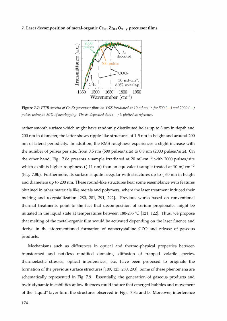
7. Laser decomposition of metal-organic Ce0:9Zr0:1O2y precursor films
Asdeposited
1350 1500 1650 1800 1950
Tran
smitt
ance
(a.u
.)
Wavenumber (cm-1)
C-H
COO-
10 mJ·cm-2,80% overlap
2000pulses
500 pulses
Figure 7.7: FTIR spectra of Ce-Zr precursor films on YSZ irradiated at 10 mJcm2 for 500 (—) and 2000 (—)
pulses using an 80% of overlapping. The as-deposited data (—) is plotted as reference.
rather smooth surface which might have randomly distributed holes up to 3 nm in depth and
200 nm in diameter, the latter shows ripple-like structures of 1-5 nm in height and around 200
nm of lateral periodicity. In addition, the RMS roughness experiences a slight increase with
the number of pulses per site, from 0.5 nm (500 pulses/site) to 0.8 nm (2000 pulses/site). On
the other hand, Fig. 7.8c presents a sample irradiated at 20 mJcm2 with 2000 pulses/site
which exhibits higher roughness (〈11 nm) than an equivalent sample treated at 10 mJcm2
(Fig. 7.8b). Furthermore, its surface is quite irregular with structures up to 〈60 nm in height
and diameters up to 200 nm. These round-like structures bear some resemblance with features
obtained in other materials like metals and polymers, where the laser treatment induced their
melting and recrystallization [280, 281, 291, 292]. Previous works based on conventional
thermal treatments point to the fact that decomposition of cerium propionates might be
initiated in the liquid state at temperatures between 180-235 ºC [121, 122]. Thus, we propose
that melting of the metal-organic film would be activated depending on the laser fluence and
derive in the aforementioned formation of nanocrystalline CZO and release of gaseous
products.
Mechanisms such as differences in optical and thermo-physical properties between
transformed and not/less modified domains, diffusion of trapped volatile species,
thermoelastic stresses, optical interferences, etc, have been proposed to originate the
formation of the previous surface structures [109, 125, 280, 293]. Some of these phenomena are
schematically represented in Fig. 7.9. Essentially, the generation of gaseous products and
hydrodynamic instabilities at low fluences could induce that emerged bubbles and movement
of the "liquid" layer form the structures observed in Figs. 7.8a and b. Moreover, interference
174

7.2. Optimization of irradiation conditions for the decomposition of CZO precursor films
(a)
(b)
RMS=0.3 nm
0.5 µmRMS=0.5 nm
0.5 µmRMS=0.8 nm
(c)
0.0 0.5 1.0 1.5 2.00.00.40.81.21.6
Hei
gth
(nm
)
Length (µm)
80% overlap10 mJ·cm-2,500 pulses
10 mJ·cm-2,2000 pulses
01234
0.0 0.5 1.0 1.5 2.0H
eigt
h (n
m)
Length (µm)
0.5 µmRMS=11 nm
20 mJ·cm-2,2000 pulses
01020304050
0.0 0.5 1.0 1.5 2.0
Hei
gth
(nm
)
Length (µm)
Figure 7.8: AFM images and corresponding profiles of precursor films irradiated with 80% of overlapping at 10
mJcm2 after applying (a) 500 and (b) 2000 pulses/site the subtrate at room temperature, and (c) 20 mJcm2
after applying 2000 pulses/site.
Gas bubbles(CO2, H2O)
CZOnanocrystals
Moltenmaterial
Figure 7.9: Schematic representation of the mechanisms involved in melting/recrystallization processes.
caused by the quasi-transparent film might also contribute to produce those ripple-like
structures [125, 291]. An enhancement of photochemical and photothermal reactions should
be expected due to the use of higher fluences. Thus, decomposition and formation of volatile
precursors would be promoted together with bubble coalescence and stronger hydrodynamic
effects. These strengthen phenomena should lead to a much more intense movement of the
175

7. Laser decomposition of metal-organic Ce0:9Zr0:1O2y precursor films
molten phase and, once solidified, to the formation of larger structures (Fig. 7.8c). Further
investigation of the mechanisms involved in the laser decomposition of metal-organic films is
required to acquire a complete picture of the phenomena causing films final microstructure,
which is beyond the scope of this work.
Fig. 7.10a shows a sample processed with 10 mJcm2, 500 pulses/site, 80% of beam
overlapping and a substrate temperature of 100 ºC. Besides obtaining a totally decomposed
precursor film, the morphological analysis by AFM unveils an extraordinary improvement to
a greater extent of its surface compared to films detailed in Fig. 7.8. Neither wave-like nor
hill-like structures are observed and films roughness has decreased to 〈0.3 nm which is
smaller than the initial roughness of the metal-organic film (Fig. 7.1). In addition, we can see
that the film morphology and roughness are comparable to films pyrolyzed at 300 ºC for 30
min using conventional furnaces.
Essentially, by rising the substrate temperature the fluid state duration with every pulse is
increased, providing extra time for the stabilization of its movement and for the exclusion of
internal bubbles leading to a smoother and more compact film. This is apparently what
temperature simulations shown in Fig. 7.5b could be indicating, i. e. a rise in the substrate
temperature during irradiation would lead to an increase of the duration of the precursor film
molten state from 5 to 20 ns due to higher temperatures achieved surpassing the melting point
0.5 µm
(a)
(b)
0.5 µmRMS=0.3 nm
RMS=0.3 nm
Laser decomposition at 10 mJ·cm-2, 80% overlap500 pulses,100 ºC
0.00.51.01.52.0
0.0 0.5 1.0 1.5 2.0
Hei
gth
(nm
)
Length (µm)
0.00.40.81.2
0.0 0.5 1.0 1.5 2.0
Hei
gth
(nm
)
Length (µm)
Furnace pyrolysis at 300 ºC for 30 min
Figure 7.10: AFM images and corresponding profiles of precursor films (a) irradiated with 80% of overlapping at
10 mJcm2 after applying 500 pulses/site with the substrate at 100 ºC, and (b) conventionally pyrolyzed at 300
ºC for 30 min.
176

7.3. Influence of laser decomposition to CZO film growth compared to furnace pyrolysis
of the CZO metal-organic precursor. Furthermore, this effect could be reinforced by
photochemical mechanisms which have not been considered in our simulations, leading to
even longer durations.
The XRD analysis of this last example confirms that laser-decomposed films are completely
nanocrystalline since its spectra is comparable to that of conventionally pyrolyzed films and no
crystalline reflections could be identified (Fig. 7.11).
25 30 35 40 4510
105
Inte
nsity
(a.
u.)
θ-2θ
104
103
102
Laserdecomposition
Furnace pyrolysis
YSZ(002)CZO(002)
CZO(111)kβ
Figure 7.11: XRD measurements of precursor films decomposed with 80% of overlapping at 10 mJcm2 after
applying 500 pulses/site with the substrate at 100 ºC (—), and conventionally pyrolyzed at 300 ºC for 30 min
(—).
7.3 Influence of laser decomposition to CZO film growth compared
to furnace pyrolysis
In order to evaluate the quality of the decomposed metal-organic films, we performed a high
temperature crystallization of the films by means of conventional thermal annealing using the
conditions described in Chapter 5, i. e. 900 ºC for 8 h, in oxygen flow.
Figs. 7.12a and b show that samples decomposed by laser with the substrate at room
temperature lead to a granular morphology when annealed at high temperatures. The grain
size and surface roughness of these annealed films is derived from that achieved during the
decomposition of the metal-organic film (Figs. 7.8 and 7.10). On the one hand, the lowest
average grain size and roughness, 180 nm and 3.8 nm, were obtained in the sample treated
with 10 mJcm2 and 500 pulses/site (Fig. 7.12a) whereas the corresponding maximum
values, 230 nm and 14 nm, respectively, were obtained in the sample irradiated with 20
mJcm2 and 2000 pulses/site (Fig. 7.12b). In addition, a high density of voids, some of them
177

7. Laser decomposition of metal-organic Ce0:9Zr0:1O2y precursor films
0.5 µm
0.5 µm
(a)
(b)
RMS=3.8 nm
RMS=14 nm
Growth at 900 ºC for 8h in O2
0.5 µmRMS=2.3 nm
10 mJ·cm-2, 500 pulsesand 100 ºC
(c)
048
12
0.0 0.5 1.0 1.5 2.0
Hei
gth
(nm
)
Length (µm)
015304560
0.0 0.5 1.0 1.5 2.0
Hei
gth
(nm
)
Length (µm)
0
15
30
0.0 0.5 1.0 1.5 2.0
Hei
gth
(nm
)
Length (µm)
10 mJ·cm-2, 500 pulses
20 mJ·cm-2, 2000 pulses
Figure 7.12: AFM images of CZO films crystallized at 900 ºC during 8 h in O2 flow after laser irradiation with
(a) 10 mJcm2 and 500 pulses/site, (b) 20 mJcm2 and 2000 pulses/site, and (c) 10 mJcm2 and 500 pulses/site
and a substrate temperature of 100 ºC.
reaching the substrate’s surface, are also visible between the grains. On the other hand, the
film crystallized after being decomposed by laser at 10 mJcm2, 500 pulses/site and the
substrate at 100 ºC (Fig. 7.12c) exhibits terraced-like features equivalent to those typically
obtained by conventional thermal treatments (Fig. 5.1a). Grain sizes are similar to CTA films,
i. e. between 100 and 150 nm, although the surface roughness is slightly larger, 2.3 nm
compared to 1 nm (Fig. 5.1a).
XRD analyses of the previous samples (Fig. 7.13) show the presence of a peak at 2 = 33:4º
corresponding to the (002) CZO reflection and no other peaks could be identified. This means
that either no polycrystalline growth exists or its overall volume is below the resolution limit of
the diffractometer employed. Furthermore, the intensity of the (002) peaks in laser processed
films is very similar to that produced by furnace pyrolysis. In addition, we could confirm that
films derived from laser decomposition have a good crystalline quality after growth at 900 ºC
for 8 h in a tubular furnace, comparable to those fully decomposed and grown by CTA.
178

7.4. Design of patterns due to local treatments
25 30 35 40 4510
105
Inte
nsity
(a.
u.)
θ-2θ
104
103
102
106
107
10 mJ·cm-2,500 pulses
10 mJ·cm-2,500 pulses, 100 ºC
CTA
20 mJ·cm-2,2000 pulses
YSZ(002)CZO(002)CZO(111)
kβ
Figure 7.13: XRD analysis of CZO films crystallized at 900 ºC during 8 h in O2 flow after laser decomposition
at 10 mJcm2 and 500 pulses/site (—), (b) 20 mJcm2 and 2000 pulses/site (—) both at room temperature, and
(c) 10 mJcm2 and 500 pulses/site and a substrate temperature of 100 ºC (—). The data for a furnace only sample
(—) is plotted for comparison.
As we demonstrated in chapters 4 and 5, the furnace pyrolysis at low temperature of ceria
precursor films leads to the presence of homogeneously and heterogeneously nucleated
grains. Further annealing at high temperature promotes heterogeneous nucleation and
growth of the epitaxial fraction. Since the epitaxial growth seems to be driven by diffusion
mechanisms, the inner microstructure of the already decomposed film will also determine the
final morphology of the crystallized film [55, 108, 190]. For this reason, some of the films
decomposed by laser which have inner voids, defects, impurities and rough surfaces,
probably due to significant liquid-layer movements, derive in a porous and rough surface
compared to the other cases. Finally, we conclude that using the optimized conditions for the
laser-induced metal-organic decomposition of films allows us to fabricate high-quality and
epitaxial CZO films with a reduced processing time. This would allow the implementation of
laser decomposition in industrial applications which employ reel-to-reel deposition
techniques and to enhance the process throughput. For example, it could be very interesting
for the production of superconducting coated conductors.
7.4 Design of patterns due to local treatments
Taking advantage of the high processing speed, high spatial resolution and decomposition
conditions optimized in the previous section, we contemplated the use of laser irradiation as
a mean to write patterns on metal-organic films for micro-fabrication. Even though in this
section we will focus on the design of ceria-based structures, this technique could become very
179

7. Laser decomposition of metal-organic Ce0:9Zr0:1O2y precursor films
appealing in fields such as superconductivity for the reduction of AC losses [294] or to define
micrometric patterns useful for electronic devices [295].
In order to investigate the capabilities of laser direct writing, we have designed a
experimental setup similar to the one presented in section 2.3.3, but including a beam
homogenizer, a square mask and a converging lens. The homogenized and masked beam has
been focused to draw squared regions of 600 by 600 νm2 in size on a ceria metal-organic film
deposited on YSZ. The irradiation conditions used are the optimum ones reported in the
previous section (10 mJcm2, 500 accumulated pulses with the substrate at 100 ºC). Once
decomposition is over, we removed the non-irradiated fraction of the precursor film using a
wet chemical etching of the sample combined with a ultrasonic bath for 10 min. The etching
agent used is a H3PO4:H2O solution in a proportion 1:10. Finally, the sample was thoroughly
cleaned with acetone and methanol.
Fig. 7.14a presents an optical microscopy image of the laser-written pattern. Additionally,
Figs. 7.14b and c show a high-resolution AFM image and line scan of the edge of a square
region after it has been chemically etched. It can be seen that the edges are quite abrupt with a
typical measured slopes around 120-180 nm/νm. The square has an average thickness of 25 nm
similar to the one obtained for pyrolyzed CZO films (section 5.3.1). No remaining precursor
material could be found on the surface of the etched fraction.
200 µm
(a) (b) (c)
0102030
0.0 1.0 2.0 3.0 4.0
Hei
gth
(nm
)
Length (µm)
Figure 7.14: (a) Image obtained from optical microscopy showing a square region of 600 by 600 νm2 in size, (b)
AFM image of one border of the pattern illustrated in (a), and (c) corresponding line scan.
Regardless, chemical etching of nanocrystalline or fully crystalline films is an open issue
for CeO2 due to its chemical inertness. Consequently, the micro-patterning of crystalline ceria
films once growth is completed, like that achieved with physical deposition methods, is still a
challenging issue which hinders the progress of device and structured coated conductor
fabrication [294, 295]. Nonetheless, the exceptional results achieved from the combination of
CSD and laser direct writing may contribute to the low-cost, versatile and time-optimized
manufacture of cerium dioxide micrometric patterns for the design of advanced devices,
180

7.5. Summary and conclusions
templates or multi-layered structures.
7.5 Summary and conclusions
In this chapter, we have shown that metal-organic (Ce,Zr)-propionate films on YSZ substrates
can be decomposed using pulsed UV laser irradiation (λ = 266 nm, θ → 3 ns).
Spectrophotometry measurements reveal that these films have a weak absorption, being
larger in the UV range. Thus, partial volume decomposition is expected to occur.
Modeling of sample heating during irradiation indicates that despite photothermal
mechanisms are important in laser-induced decomposition, photochemical processes may
have a large contribution too. The surface topography of precursor films seems to indicate a
transition to a molten state during irradiation which would be in agreement with the
temperatures reached.
Controlling parameters such as fluence, number of pulses and substrate temperature is vital
to achieve both, optimal decomposition and surface morphology. At high fluences, a rough film
surface has been obtained probably due to vigorous movements of the liquid phase and bubble
formation. On the other hand, low fluences derive in quite smoother surfaces.
Even though high quality epitaxial (001)CZO films have been obtained at high
temperatures, the surface morphology was deeply affected by the structure of films after the
decomposition step. The optimal decomposition conditions to produce films with a quality
equivalent to the one achieved in conventional thermal annealing are 10 mJcm2, 500
pulses/site, 80% of beam overlapping and a substrate temperature of 100 ºC. The combination
between CSD and the high spatial resolution of lasers was used to produce square-shaped
patterns of 600 by 600 νm2 in size with good lateral resolution.
Altogether demonstrates that laser-induced decomposition of chemically-derived films
offers a significant improvement over conventional techniques by providing a low cost,
versatile, straightforward and less time-consuming approach to obtain epitaxial CZO films
and patterns.
181

7. Laser decomposition of metal-organic Ce0:9Zr0:1O2y precursor films
182

Chapter 8
Laser-induced crystallization of oxide
thin films from CSD precursors
The crystallization of oxide films has become a central topic in materials science due to the
outstanding functional properties and associated potential applications already described
[3, 5, 10, 13, 32, and references therein]. Even though it has been demonstrated that chemical
solution deposition (CSD) is able to compete under equal conditions or even surpass in some
aspects physical techniques, certain limitations must be overcome such as long processing
times, issues arising at low substrate temperature or straightforward spatially-resolved
crystallization. In this sense, pulsed laser annealing (PLA) of CSD deposited precursors has
been recently proven an exceptional complementary methodology to go beyond the
limitations of pure thermal techniques and produce crystalline or even epitaxial oxide thin
films. Regardless of the potential shown, very few works have been dedicated to explore the
epitaxial growth of oxide heterostructures using UV pulsed-laser irradiation of CSD precursor
films, and the underlying mechanisms are still unknown [70, 72, and references therein].
In this chapter, we intend to investigate the solid-state crystallization of multiple
functional oxide thin films deposited by CSD (CZO, LNO, BST and LSMO) on (001)-oriented
single crystal (YSZ, LAO and STO) and technical substrates ((001)YSZ/stainless steel and
LNO-coated silicon wafers), and apply the different methodologies developed in previous
chapters to provide more insight into the still unknown mechanisms governing nucleation
and growth processes in laser crystallization of CSD precursor films.
183

8. Laser-induced crystallization of oxide thin films from CSD precursors
8.1 CZO thin-films: a model system for laser crystallization
So far, doped cerium oxide has been the common material of this thesis in each of the topics
investigated due to its simple composition, its wide use in many applications, and the existing
knowledge in our group. Since laser crystallization of oxides from CSD precursor films is a
very novel methodology, it seems logical to firstly investigate the growth of CZO films in order
to utilize it as a model system for the crystallization of more complex multicomponent oxides.
It must be noted that all irradiation experiments will be performed in air.
Among the wide range of applications where cerium oxide is employed [1, 16, 17] already
mentioned in previous chapters, it has been chosen here due to its integration in
high-temperature superconducting coated conductor architectures [21].
We have shown in Chapter 7 that laser annealing can be applied to achieve the
decomposition of cerium-zirconium precursor films to form nanocrystalline CZO films with
high surface flatness. In this section, we will go a step further and study the influence of
multiple laser parameters (fluence, substrate temperature, degree of overlapping and number
of pulses) in the morphology and epitaxial crystallization of CZO films on (001)YSZ
substrates, comparing it with samples produced using thermal treatments. Ultimately, we will
evaluate the growth of epitaxial CZO films on (001)YSZ-buffered stainless steel substrates for
the implementation of laser irradiation in the production of high-temperature
superconducting coated conductors.
8.1.1 Evaluation of experimental conditions
The nanocrystalline CZO film obtained after decomposition of metal-organic precursors,
which will be irradiated by laser, mainly consists of Ce-O and Zr-O bonds, and probably
dangling bonds associated to crystalline defects. As Table 8.1 illustrates, the dissociation
energies of Ce-O and Zr-O bonds are significantly larger than the energy of the photons
emitted by the Nd:YAG laser (〈4.7 eV at 266 nm) although this values may change depending
on the particular electronic environment. Therefore, it seems logic to assume that thermal
interactions are the main source contributing to heating. Despite that, photochemical
processes cannot be completely discarded since they may be particularly strong at crystalline
defects due to their low bond dissociation energies.
The evaluation of the photothermal effect taking into account the thermo-physical and
optical properties of the different constitutive materials (Table 6.1) is done employing
184

8.1. CZO thin-films: a model system for laser crystallization
Table 8.1: Dissociation energy of the chemical bonds present in CZO thin-films. Data extracted from [296].
Chemical bond Dissociation energy (kJmol1)
Ce-O 795 (〈8.3 eVbond1)
Zr-O 760 (〈7.9 eVbond1)
numerical simulations (section 6.3). These calculations together with experimental evidence
should help us to ascertain the optimal irradiation conditions like laser fluence, substrate
temperature, etc.
Because the heat produced in the system is based on the absorption of photons, measuring
the optical properties of the already decomposed Ce-Zr propionate film is of vital importance
to achieve crystallization. In Fig. 8.1, we present the measured reflectance and transmittance
spectra of fully decomposed CZO precursor films on Al2O3 substrates, as well as the optical
parameters (n, η, and l) derived employing the methodology described in section A.4.2.
The alumina substrate has been chosen because it is optically transparent at the range of
wavelengths considered. We can see in Fig. 8.1a that the transmittance increases with the
wavelength, and has a relative minimum value at λ〈275 nm. On the other hand, the
reflectance increases from 0 to 10% when λ diminishes. Likewise, Fig. 8.1b shows that the
refractive index n experiences an increase from 2.1 to 2.8 between 200 and 1100 nm, whilst the
extinction coefficient η varies from 0.2 to 0.7. Both parameters also have a relative maximum
value at λ〈275 nm. The value of η in the near infrared and visible regions are above those
typically obtained, which is probably caused by the high density of structural defects present
inside these films, as reported in the literature [297, 298]. Finally, Fig. 8.1c shows that the
absorption coefficient has a decreasing trend with the wavelength and a relative maximum
also at 275 nm. The overall values of CZO are one order of magnitude larger than those
(a) (b)
0
20
40
60
80
100
%
200 400 600 800 1000Wavelength (nm)
Transmittance
Reflectance
(c)
0.0
0.5
2.0
2.5
3.0
Refractiveindex, n
Extinctioncoefficient, κ
200 400 600 800 1000Wavelength (nm)
024
153045
200 400 600 800 1000
α(1
06 m-1)
Wavelength (nm)
l α(1
02 nm
)
Figure 8.1: Optical properties of pyrolyzed precursor film deposited on -Al2O3 substrate. (a) Measured
transmittance and reflectance spectra, (b) calculated refractive index and extinction coefficient and (c) optical
absorption coefficient and penetration depth.
185

8. Laser-induced crystallization of oxide thin films from CSD precursors
measured for precursor films (section 7.1), indicating the need to always evaluate the optical
properties of each system. For instance, CZO〈31106 m1 at 266 nm, while precursor〈4106
m1 (Table 6.1). The corresponding optical penetration depth for the pyrolyzed film is
lCZO 〈32 nm at λ=266 nm which is slightly higher compared to the effective film thickness
considered, i. e. 〈20 nm (section 5.3.1). In these circumstances, only a 〈47% of the incoming
laser intensity is absorbed by the film, and hence, the YSZ substrate could contribute to
heating and crystallization.
The optical properties of YSZ single crystalSCYSZ
substrates have been measured by
ellipsometry following the procedure explained in section A.4.3 and are presented in Fig. 8.2.
Data for YSZ grown by ABAD on stainless steelABADYSZ
is reported for completeness with
the experiments shown in section 8.1.3. Fig. 8.2a shows that the refractive index of SCYSZ
decreases approximately from 2.8 to 2.2 with the wavelength, while it varies from 2.2 to 1.8 forABADYSZ showing a maximum value at λ〈335 nm. On the other hand, the extinction
coefficient is reduced from 0.3 to 4104 and from 0.07 to 7104 for SCYSZ and ABADYSZ,
respectively. Likewise, Fig. 8.2b illustrates a decreasing trend of the absorption coefficient
with the wavelength for both YSZ systems. The absorption coefficient of SCYSZ is
Y SZSC=4105 m1 at 266 nm which corresponds to an optical penetration depth
lY SZSC =2:5 νm. This means that a 63% of the radiation intensity reaching the film-substrate
interface is absorbed inside the SCYSZ through a thickness equivalent to lY SZSC . Therefore,
the contribution of the SCYSZ substrate to film heating will be scarce.
It is worth noting that the YSZ layer deposited on stainless steel substrates by ABAD
200 400 600 800 10000.00.10.21.62.02.42.8
n
Wavelength (nm)
κ
YSZ SCYSZ ABAD
(a) (b)
200 300 400 500 6000.00.51.01.52.02.53.03.54.0
Wavelength (nm)
α (
106 m
-1)
YSZ SC
YSZ ABAD
266 nm
Figure 8.2: Optical properties of YSZ in single crystal (solid circles) and on metallic substrates (solid circles). (a)
Refractive index (n) and extinction coefficient (η), (b) optical absorption coefficient (). Data was obtained from
ellipsometry measurements detailed in section A.4.3.
186

8.1. CZO thin-films: a model system for laser crystallization
displays an optical absorption at 266 nm three times larger than Y SZSC
(Y SZABAD=1:2106 m1) leading to a lY SZSC =800 nm, similar to its thickness (〈1 νm).
Such absorption, probably due to the presence of crystalline defects in the film, will cause a
larger contribution to the overall heating than the SCYSZ substrate which will have
consequences to the laser crystallization of CZO, as we will see later on. The reader is referred
to section 8.1.3 for further details.
8.1.1.1 Influence of laser fluence on CZO film crystallization on SCYSZ substrates
The pulse temporal evolution, considered as a Gaussian with a FWHM duration of 〈3 ns, the
laser fluence, the optical absorption and the thermo-physical properties of each material will
mostly define the temperature distribution along the heterostructure. Temperatures achieved
in the CZO/SCYSZ system at different fluences (Fig. 8.3) have been modeled as described in
section 6.3. It can be seen that the laser pulse generates a thermal cycle with a duration of tens
to hundreds of nanoseconds. In addition, this fast pulses lead to heating/cooling rates as fast
as 1011 and 109 ºCs1, respectively. The cooling process is usually some orders of magnitude
longer than heating because the substrate acts as a thermal barrier impeding heat evacuation,
i. e. its thermal conductivity is very small (Table 6.1). Temperature profiles after applying a
single pulse with fluences between 20 and 80 mJcm2, and keeping the substrate at room
temperature (Fig. 8.3a) show that peak temperatures increase linearly with the fluence from
〈750 ºC to 3000 ºC (Fig. 8.3b), respectively. Notice that temperatures above the melting point
of CZO (TCZOmp 〈2400 ºC) could be overestimated because variation of thermo-physical
parameters and latent heat of melting have not been considered. Despite temperatures at the
CZO/YSZ interface are 〈50-300ºC lower than at the CZO surface for times close to the peak
maximum (Figs. 8.3a and b), they never go beyond the melting point of YSZ (T Y SZmp 〈3000 ºC).
Large temperature gradients of 1010 ºCm1 which last few nanoseconds are calculated due to
the difference between surface/interface temperatures in 20 nm-thick films. Finally, Fig. 8.3c
shows that the effective heating time teff, defined as the amount of time the system is above
600 ºC (section 6.3), also becomes longer as the energy input rises.
Simulations have been used as an experimental guide. We have applied laser fluences
ranging from 20 to 80 mJcm2 at the center of different nanocrystalline CZO films on SCYSZ.
Figs. 8.4a-d illustrate a quite granular surface morphology for laser-annealed films after 1000
pulses. These spherical-like grains could be an indication of polycrystalline material as we
reported in section 5.3.4. Moreover, we observe the formation of larger and more planar
187

8. Laser-induced crystallization of oxide thin films from CSD precursors
(a) (b)
0500
10001500200025003000
Tem
pera
ture
(ºC
)
0.1 1 10 100 1000Time (ns)
80 mJ·cm-2
60 mJ·cm-2
40 mJ·cm-2
20 mJ·cm-2
Laserpulse
Tmp=2400 ºC
20 40 60 80500
1000
1500
2000
2500
3000
Max
. tem
p. (
ºC)
Fluence (mJ·cm-2)
Surface
Interface
(c)
20 40 60 8010
20
30
40
Effe
ctiv
e he
atin
gtim
e, t e
ff (n
s)
Fluence (mJ·cm-2)
Figure 8.3: (a) Temperature profiles of 20 nm-thick CZO films on YSZ substrates at room temperature for fluences
of 20 mJcm2 (—), 40 mJcm2 (—), 60 mJcm2 (—) and 80 mJcm2 (—), and laser pulse (—). The solid
and dashed lines are representative of surface and interface profiles, respectively. Dependence of (b) surface and
interface maximum temperatures, and (c) the effective heating time with the laser fluence.
regions of tens of nanometers with rounded contours for a fluence of 80 mJcm2, highlighted
in red (Fig. 8.4d). Comparable rounded grains have also been detected for different materials
such as metals, semiconductors and polymers in works dedicated to investigate laser melting
and resolidification processes [280, 281, 291, 299]. Thus, these features may indicate that the
system has transitioned to a molten state and, then, recrystallized during cooling since
temperatures above TCZOmp =2400 ºC could be reached for a fluence of 80 mJcm2 (Figs. 8.3a
and b).
XRD analysis in Fig. 8.4e reveals the presence of mostly epitaxially-oriented material, as
well as some polycrystalline fraction, as respectively indicated by the (002)CZO and (111)CZO
orientations. Thus, some degree of crystallization and even epitaxy is reached after laser
annealing at the fluences investigated and after the application of 1000 pulses. Furthermore,
we can see a slight increase in intensity from 20 to 80 mJcm2. Given these results, additional
improvement of the experimental conditions is still required in order to achieve a degree of
crystallization similar to that reported for conventional thermal annealing at 900 ºC, 10
188

8.1. CZO thin-films: a model system for laser crystallization
0.5 µm 0.5 µm
0.5 µm
20 mJ·cm-2,1000 pulses
40 mJ·cm-2,1000 pulses
60 mJ·cm-2,1000 pulses
80 mJ·cm-2,1000 pulses
(a) (b)
(c) (d)
(e)
25 30 35 40 45
(002)CZO(002)YSZ
900 ºC,8h (CTA)
60 mJ·cm-2
20 mJ·cm-2
40 mJ·cm-2
80 mJ·cm-2
1
102
103
Inte
nsity
(a.
u.)
-2 (º)
10
YSZ kβ
(111)CZO
104
1000 pulses
105
106
107
0.5 µm
Figure 8.4: AFM images of CZO thin-films grown on YSZ by laser crystallization after 1000 pulses at (a) 20,
(b) 40, (c) 60 and (d) 80 mJcm2. Irradiation was performed at the center of the sample. The red areas in (d)
correspond to possibly molten material. (e) XRD analysis of laser crystallized samples at 20 (—), 40 (—), 60
(—) and 80 (—) mJcm2 after 1000 pulses applied at the center of the sample. Data from a sample grown using
conventional thermal annealing at 900 ºC, 10 ºCmin1 for 8 h (—) is plotted for comparison.
ºCmin1 for 8 h. In the next sections, we will approach this issue.
8.1.1.2 Influence of the degree of beam overlapping on the CZO film crystallization
Since the laser beam has a nearly gaussian shape, i. e. the fluence significantly decreases
radially following a gaussian distribution. Consequently, the induced crystallization derived
from such spatial distribution may vary considerably. We expect that irradiating with the
same number of pulses adjacent areas besides the sample’s center will lead to more
homogeneous films and boost crystallization farther. Figs. 8.5a-c present the surface
morphology of films irradiated at 80 mJcm2 with the substrate at room temperature
(melting conditions), applying 1000 pulses and changing the degree of overlapping from 0 to
80%. The presence of rounded features rises with the degree of overlapping and the surface
becomes rougher, i. e. the RMS roughness goes from 4.2 to 6.9 nm. Although the mechanisms
governing the rise in surface roughness are still unclear, we propose that phenomena like
thermal gradients, thermocapillary movements and different thermo-mechanic behavior of
material with distinct degree of conversion could have an influence on the flow of molten
material and lead to higher structures and roughness, as it has been previously observed in
the literature [125].
Despite surface morphology becomes rougher, 2 scans shown in Fig. 8.5d seem to
189

8. Laser-induced crystallization of oxide thin films from CSD precursors
0.5 µm 0.5 µm0.5 µm
(a) (b) (c)0% overlap 60% overlap 80% overlap
RMS=4.2 nm
RMS=6.8 nm
RMS=6.9 nm
0 % overlap
60 % overlap
80 % overlap
25 30 35 40 45
102
103
104
Inte
nsity
(a.
u.)
-2 (º)
10
105
(002)YSZ
(002)CZO
1
YSZ kβ
(111)CZO
(d) (e)
0 20 40 60 800.04
0.06
0.08
0.10
0.12
Overlap (%)
Nor
mal
ized
(00
2)pe
ak a
rea
(a.u
.)
Figure 8.5: AFM images illustrating the surface morphology of CZO thin-films grown on YSZ by laser
crystallization at 80 mJcm2 and 1000 pulses/site for (a) 0%, (b) 60% and (c) 80% of overlapping. (d) XRD
analysis and (e) corresponding (002) peak area of laser crystallized samples at 80 mJcm2 after applying 1000
pulses/site for different degrees of beam overlapping: 0% (—), 60% (—) and 80% (—) of overlapping. These
values are normalized to the (002) peak area of a sample grown by CTA after 8 h at 900 ºC.
indicate an enhancement in films crystallinity from 0 to 80% of overlapping. In fact, the
normalized integrated area of the (002)CZO peak reveals an increase from 〈0.05 at 0% of
overlapping to 0.11 at 80% of overlapping (Fig. 8.5e). Bear in mind that the (002) integrated
area is small because it has been normalized to the integrated area of a sample obtained by
CTA after 8 h at 900 ºC. As we mentioned in section 5.3.4, these figures not only provide
information about the quantity of epitaxial material in CZO films, but also are highly
influenced by nanocrystals size and crystallinity.
8.1.1.3 Influence of the number of pulses on CZO film crystallization
The application of a large number of pulses may also contribute to increase crystallinity of
the CZO film. In this case, we performed the irradiation using a fluence of 80 mJcm2, an
overlapping of 80%, the substrate at room temperature and increased the number of pulses/site
up to 7000. Indeed, Figs. 8.6a-c reveal that the molten-like features observed after applying
1000 pulses cover a larger area of the film’s surface and, eventually, seem to transform into
more polyhedral-like shaped structures after the accumulation of a large number of pulses.
190

8.1. CZO thin-films: a model system for laser crystallization
0.5 µm 0.5 µm0.5 µm
(a) (b) (c)1000 pulses 3000 pulses 7000 pulses
RMS=6.9 nm
RMS=4.3 nm
RMS=4.7 nm
(d) (e)
7000 pulses
3000 pulses
1000 pulses
25 30 35 40 45
102
103
104
Inte
nsity
(a.
u.)
-2 (º)
10
105
1
106
(002)YSZ(002)CZO
YSZ kβ
(111)CZO
10-4 10-3 103 104
0.00.20.40.60.81.0
Nor
mal
ized
(00
2)pe
ak a
rea
(a.u
.)
Effective heating time (s)
PLA
CTA1.5 ms(7000 pulses)
30’4 h
8 h
Figure 8.6: CZO thin-films grown on YSZ by laser crystallization at 80 mJcm2 with an 80% of overlapping.
AFM images after applying (a) 1000, (b) 3000 and (c) 7000 pulses/site. (d) 2 scans after for 1000 (—), 3000
(—) and 7000 (—) pulses/site, and (e) (002)-peak integrated area normalized with respect to a sample grown using
CTA at 900 ºC, 10 ºCmin1 and 8 h. CTA (orange circles) data is plotted for comparison.
This leads to a reduction in the RMS roughness from 6.9 to 4.7 nm.
Fig. 8.6d presents the 2 scans of films irradiated with 1000, 3000 and 7000 pulses/site.
We can identify both the epitaxial (002)CZO and the polycrystalline (111)CZO orientations.
The integration of the (002) peak area, normalized to a sample produced by CTA as mentioned
before, is presented as a function of the effective heating time in Fig. 8.6e. The overall effective
heating time for laser-crystallized samples has been calculated from the simulated teff for a
single pulse as indicated in section 6.3.2 and multiplying by the accumulated number of
pulses. Since we must take into account the contribution of overlapping, we also added the
effective heating time corresponding to the fluence at the center of laser spots coming from
adjacent pulses (up to 3 neighbors). The normalized area grows very slowly and after 1.5 ms
(7000 pulses/site) of irradiation it has a value of 0.13. Although these numbers are really low
compared to those obtained by CTA, it must be noticed that teff is approximately 7-8 orders of
magnitude lower.
191

8. Laser-induced crystallization of oxide thin films from CSD precursors
8.1.1.4 Influence of substrate temperature on CZO film crystallization
The obtention of smoother surfaces is usually mandatory for several technological and
industrial applications. Hence, solid-state laser processing, i. e. laser crystallization at
fluences reaching a maximum temperature beneath the melting point, may prove
advantageous in reducing films’ roughness and promoting homogeneous surfaces.
For this purpose, we performed irradiation at a fluence of 40 mJcm2 which is far below
melting, TCZOmp =2400 ºC, (Fig. 8.7a) with an 80% of overlap and accumulating 1000
pulses/site. Moreover, the substrate temperature was set at different values, i. e. room
temperature, 200 and 400 ºC, in order to evaluate its contribution to the crystallization of CZO.
Fig. 8.7b indicates that the maximum peak temperature increases linearly with the substrate
temperature and should not exceed TCZOmp at the aforementioned experimental conditions. In
addition, the effective heating time increases non-linearly with the substrate temperature (Fig.
8.7c), so we may expect an improvement in crystallization at higher values of Tsubstrate.
(a) (b)
0
400
800
1200
1600
2000
0.1 1 10 100 1000
Tem
pera
ture
(ºC
)
Time (ns)
400 ºCLaser pulse(τ∼3 ns)
200 ºCRoomTemp.
RT 200 4000
20
40
60
80
Effe
ctiv
e he
atin
gtim
e, t
eff (
ns)
Substrate temperature (ºC)
(c)
RT 200 4001400
1500
1600
1700
1800
1900
Max
. tem
p. (º
C)
Substrate temperature (ºC)
Figure 8.7: (a) Temperature simulation of 20 nm-thick CZO film on YSZ. The fluence was set to 40 mJ cm2 and
the substrate at room temperature (—), 200 ºC (—) and 400 ºC (—). The laser pulse (—) is plotted as a reference.
(b) Maximum temperature and (c) effective heating time dependence with substrate temperature extracted from
(a) as explained in section 6.3.2.
192

8.1. CZO thin-films: a model system for laser crystallization
Figs. 8.8a-c show that films surface morphology is composed of small and spherical grains
and the RMS roughness diminishes with the substrate temperature from 〈1.5 nm at RT to
〈0.8 nm at 400 ºC. XRD analyses presented in Figs. 8.8d and e clearly evidence that the
intensity and normalized area of the (002)CZO peak increase with substrate temperature. This
boost in the degree of crystallization could be produced by the longer heating times
developed achieved due to the rise in the substrate base temperature (Fig. 8.7c). It should be
noted that a 2 scan of a sample annealed at 400 ºC for 1h presents no CZO peaks,
indicating that the crystallization achieved without laser irradiation at these experimental
conditions is negligible. Hence, subsequent PLA experiments of CZO films will be done with
a substrate temperature of 400 ºC.
0.25 µm 0.25 µm
(a) (b) 200 ºC
RMS=1.5 nm
RMS=1.1 nm 0.25 µm
400 ºC
RMS=0.8 nm
(c)RT
25 30 35 40 45
102
103
104
Inte
nsity
(a.
u.)
-2 (º)
10
105
1
106
200 ºC400 ºC
RT
(002)YSZ(002)CZOYSZ kβ
(111)CZO
400 ºC, 1h
(d) (e)
0.00
0.05
0.10
0.15
RT 200 400
Nor
mal
ized
(00
2)pe
ak a
rea
(a.u
.)
Substrate temperature (ºC)
Figure 8.8: CZO thin-films grown on YSZ by laser crystallization at 40 mJcm2, 80% of overlapping, 1000
pulses/site. AFM images for samples grown with the substrate at (a) room temperature, (b) 200 ºC and (c) 400
ºC. (d) 2 scans for laser irradiated films with the substrate at room temperature (—), 200 ºC (—) and 400 ºC
(—). Data for a sample pyrolyzed at 400 ºC for 1 h using CTA (—) has been plotted for comparison. (e) (002)-peak
integrated area normalized with respect to a sample grown using CTA at 900 ºC, 10 ºCmin1 and 8 h.
8.1.2 CZO epitaxial evolution at the optimized laser annealing conditions
The optimization of the different experimental parameters involved indicates that the best
conditions to perform pulsed laser annealing of CZO films on YSZ single crystals are 40
193

8. Laser-induced crystallization of oxide thin films from CSD precursors
mJcm2, 80% of beam overlapping and a substrate temperature of 400 ºC. Figs. 8.9a-d present
the surface morphology after the accumulation of 1000, 5000, 10000 and 20000 pulses/site. It
can be seen that the surface is quite granular with grain sizes of tens of nanometers. In all
cases, the RMS roughness is kept almost constant at 〈0.7 nm. On the one hand, this granular
morphology contrasts with the terraced-like aspect after a long-time thermal treatment.
Regardless, their morphology bears some resemblance with the early stages of kinetic
evolution as shown for samples grown by RTA (Fig. 5.17a). In fact, we hypothesize that longer
irradiation times may end up with a terraced surface. On the other hand, the smooth surface
morphology of these samples compared to those reported in Fig. 8.6 would prove that solid
state laser crystallization is better than melting-recrystallization processes for the
implementation of these films in technological applications.
2 scans in Fig. 8.9e show that the (002)CZO peak is quite strong compared to the (111)
reflection. In addition, the intensity of the (002) peak increases with the number of pulses as it
has been pointed out previously, whereas the peak corresponding to the (111) orientation seems
to disappear. Indeed, the (002) peak normalized area (Fig. 8.9f) illustrates the rise in intensity
0.25 µmRMS=0.6 nm 0.25 µm
RMS=0.7 nm
RMS=0.8 nm 0.25 µm
RMS=0.7 nm 0.25 µm
(e) (f)
20000 pulses
1000 pulses5000 pulses
10000 pulses
25 30 35 40 45
102
103
104
Inte
nsity
(a.
u.)
-2 (º)
10
105106
107
(002)YSZ(002)CZO
YSZ kβ
(111)CZO
10210-4 10-3 104
0.00.20.40.60.81.0
Nor
mal
ized
(00
2)pe
ak a
rea
(a.u
.)
Effective heating time (s)
PLA
CTA
7.2 ms(20000 pulses)
30’4 h
8 h
103 105
30’
15’RTA
10’
5’1’
10-2
1000 pulses(a) 5000 pulses(b) 10000 pulses(c) 20000 pulses(d)
Figure 8.9: Laser crystallization of CZO thin-films on YSZ at 40 mJcm2, 80% of overlapping and 400 ºC of
substrate temperature. AFM images show the morphology after applying (a) 1000, (b) 5000, (c) 1000 and (d)
20000 pulses/site. (e) 2 scans of samples irradiated with 1000 (—), 5000 (—), 10000 (—) and 20000 (—)
pulses/site, and (f) (002)-peak integrated area normalized with respect to a sample grown using CTA at 900 ºC, 10
ºCmin1 and 8 h. RTA (red circles) and CTA (orange circles) data are plotted for comparison.
194

8.1. CZO thin-films: a model system for laser crystallization
with the effective heating time; having a ratio around 0.35 after 20000 pulses/site (〈7.2 ms of
effective heating time) which is quite similar to that obtained for a CZO film annealed with
RTA for 10 min (〈0.45). Despite that, this results are still far from those obtained with CTA at
900 ºC for 8h, and thus, reaching an equivalent crystalline quality and grain size would require
longer processing times. These results suggest that growth of high quality epitaxial CZO by
laser annealing is feasible and may be influenced by faster kinetic mechanisms than the ones
involved in thermal treatments.
As we mentioned in Chapter 5, the intensity of the (002)CZO peak not only accounts for
the epitaxial material present in our film but also its crystalline quality and grain size. Thus,
the calculation of the epitaxial fraction using 2D-XRD is more appropriate. Fig. 8.10a
illustrates the epitaxial fraction evolution with the effective heating time of CZO films
irradiated at 40 mJcm2, 80% of overlapping and a substrate temperature of 400 ºC. The
percentage of epitaxial fraction is calculated over the sum of polycrystalline and epitaxial
material, and it has been extracted from 2D images equivalent to that depicted in Fig. 8.10b as
explained in section A.3.1. Once more, these results demonstrate the conversion from a
polycrystalline matrix to an epitaxial film. We can see that the epitaxial fraction rises from
〈20% at 360 νs (1000 pulses/site) to 〈50-55% at 7.2 ms (20000 pulses/site). Furthermore, the
epitaxial fraction at 7.2 ms is comparable to that reached with a sample processed with RTA
for 10 min (〈65%), but smaller than samples annealed above 15 min which are almost fully
(a) (b)1000 pulses
(220)YSZ (220)CZO(random)
(220)CZO(epitaxial)
0 5 10 15 200
20
40
60
80
100
Epita
xial
Frac
tion
(%)
Effective heating time (ms)
0 300 600 900 1200 1500 1800Annealing time (s)
PLA
RTA
7.2 ms(20000 pulses)
τ∼420 s
τ∼7.7 ms
Figure 8.10: Epitaxial fraction calculation for CZO grown on (001)YSZ by laser annealing at 40 mJcm2, 80%
of overlapping and 400 ºC of substrate temperature as a function of the effective heating time (blue circles). RTA
data is plotted for comparison (red squares). Notice the differently colored axes for RTA and PLA methodologies.
Data fitting employing Eq. 3.22 is represented by the (blue) and (red) curves, respectively. (b) 2D-XRD image
centered at (022) for a sample treated with 1000 pulses/site.
195

8. Laser-induced crystallization of oxide thin films from CSD precursors
epitaxial.
HRTEM analyses were performed for samples irradiated at 40 mJcm2, 80% of
overlapping, a substrate temperature of 400 ºC and after applying 1000 and 20000 pulses/site.
Fig. 8.11a shows that after 1000 pulses/site the film consists mostly of randomly oriented
nanocrystals as depicted in the power spectrum in the form of rings with dimensions between
3 and 8 nm. Nevertheless, a very small fraction of the film at the interface with the substrate is
epitaxially grown with the (001)CZO orientation. This epitaxial fraction is 2-3 nm thick,
equivalent to a 〈15% of the whole film thickness. By increasing the number of pulses/site to
20000 (Fig. 8.11b), the epitaxial fraction of the film increases at expenses of the randomly
oriented grains up to a 40-50% of the total film thickness. It is worth mentioning that these
results are in agreement with those reported by XRD (Fig. 8.10) which indicates the accuracy
of the measurements performed.
Fitting of the epitaxial fraction data using a self-limited growth function (Eq. 3.22), blue
curve in Fig. 8.10a, reveals that the characteristic time for epitaxial crystallization, i.e. the time
(a)
(b)
111
200220
Polycrystalline CZO(200)
(220)
(020)
[100]CZO||[100]YSZ
1000
pul
ses
∼3-8 nm
∼2 nm
5 nm
(001)YSZ
CZO
2000
0 pu
lses
∼4-9 nm
(001)YSZ
CZO(020)
(002)(220)
Polycrystalline CZO
[100]CZO||[100]YSZ
Figure 8.11: HRTEM images and power spectra of samples obtained by irradiation of CZO pyrolyzed films
deposited on YSZ SC with 40 mJcm2, 80% of overlapping, 400ºC of substrate temperature and (a) 1000, and
(b) 20000 accumulated pulses per zone.
196

8.1. CZO thin-films: a model system for laser crystallization
needed to reach a 63% (11=e) of epitaxy, by laser processing is θCZO;SClaser;epi 〈7.7 ms. This value
is 4-5 orders of magnitude shorter than that of thermal treatments (θCZO;SCthermal;epi〈420 s at 900
ºC), red curve in Fig. 8.10a. Despite it is clear that the epitaxial growth of CZO films on YSZ
single crystals can be obtained by PLA, a larger number of pulses should be applied to obtain a
completely epitaxial film. Extrapolation from the data in Fig. 8.10a shows that after 50 ms, i. e.
accumulating 〈140000 pulses/site, full epitaxy should be reached. Even though the effective
time required is indeed shorter than for thermal treatments (〈1800 s), a high repetition rate
laser system would be required to achieve competitive processing times.
Previously, we have mentioned that the pathway transformation from nanocrystalline
grains to epitaxial ones is driven by the reduction in the Gibbs free energy (Fig. 3.12), as well
as their lower surface to volume ratio. Since epitaxial crystallization proceeds by grain
boundary reconstruction, a thermally-activated atomic diffusion process seems also essential
for that transformation to happen (section 5.3.4). Calculation of the laser epitaxial diffusion
coefficient has been done from Eq. 3.23, employing a film thickness of 20 nm and the
characteristic time θCZO;SClaser;epi obtained before from data fitting (Fig. 8.10a). Then, the effective
diffusion coefficient is DCZO;SClaser;epi 〈1:31014 m2s1 which is between 4 and 5 orders of
magnitude higher than the diffusion coefficient for thermal annealing (DCZO;SCthermal;epi〈2:41019
m2s1).
We have also calculated the epitaxial growth rates by transforming the epitaxial fraction in
Fig. 8.10a to epitaxial thickness by using a final value of 20 nm (section 5.1), and deriving the
fitting functions with time. Fig. 8.12a illustrates that the epitaxial growth rate for
laser-annealed samples at 40 mJcm2 and 400 ºC of substrate temperature decreases with the
effective heating time from 〈2500 to 200 nms1 in 20 ms, whereas it decays from 〈0.05 to 0
nms1 in 〈1800 s for samples produced by RTA at 900 ºC. Notice that the initial growth rate
for laser treatments is 4-5 orders of magnitude larger than conventional thermal treatments
(〈2500 nms1 compared to 0.05 nms1), similarly to what we reported for the characteristic
times and diffusion coefficients. The reduction in the epitaxial growth rate with time may
indicate that the conversion from polycrystalline to epitaxial material is slowed down as the
polycrystalline material available to transform diminishes, i. e. the growth rate decreases
linearly as the epitaxial thickness grows (Fig. 8.12b). It is important to highlight that the
model imposes that the growth rate must be zero when the whole film is epitaxially
transformed.
Several mechanisms may cause this large difference in characteristic times, diffusion
197
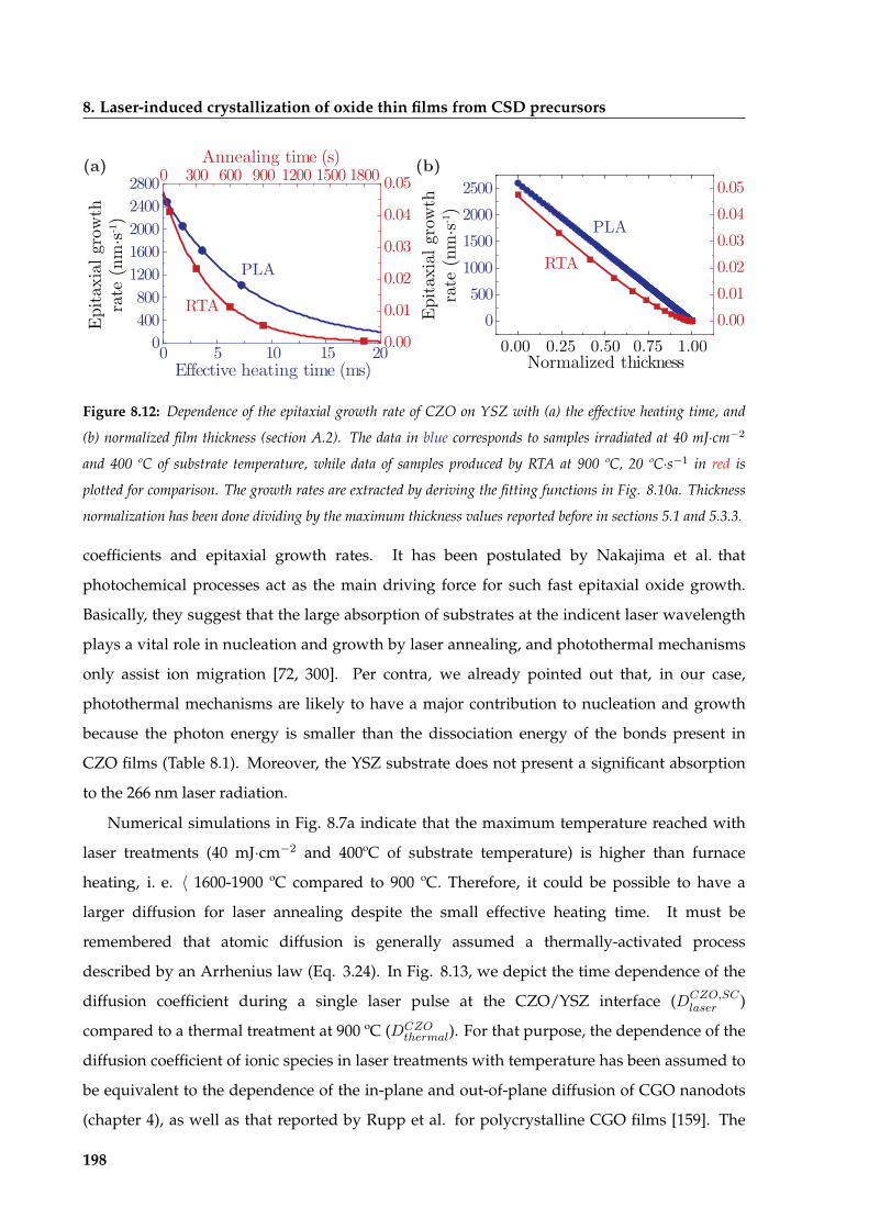
8. Laser-induced crystallization of oxide thin films from CSD precursors
(a) (b)
0400800
12001600200024002800
0.00
0.01
0.02
0.03
0.04
0.05
0 5 10 15 20
Effective heating time (ms)
0 300 600 900 1200 1500 1800Annealing time (s)
Epita
xial
gro
wth
rate
(nm
·s-1)
PLA
RTA0
5001000150020002500
0.000.010.020.030.040.05
Epita
xial
gro
wth
rate
(nm
·s-1)
PLA
RTA
0.00 0.25 0.50 0.75 1.00Normalized thickness
Figure 8.12: Dependence of the epitaxial growth rate of CZO on YSZ with (a) the effective heating time, and
(b) normalized film thickness (section A.2). The data in blue corresponds to samples irradiated at 40 mJcm2
and 400 ºC of substrate temperature, while data of samples produced by RTA at 900 ºC, 20 ºCs1 in red is
plotted for comparison. The growth rates are extracted by deriving the fitting functions in Fig. 8.10a. Thickness
normalization has been done dividing by the maximum thickness values reported before in sections 5.1 and 5.3.3.
coefficients and epitaxial growth rates. It has been postulated by Nakajima et al. that
photochemical processes act as the main driving force for such fast epitaxial oxide growth.
Basically, they suggest that the large absorption of substrates at the indicent laser wavelength
plays a vital role in nucleation and growth by laser annealing, and photothermal mechanisms
only assist ion migration [72, 300]. Per contra, we already pointed out that, in our case,
photothermal mechanisms are likely to have a major contribution to nucleation and growth
because the photon energy is smaller than the dissociation energy of the bonds present in
CZO films (Table 8.1). Moreover, the YSZ substrate does not present a significant absorption
to the 266 nm laser radiation.
Numerical simulations in Fig. 8.7a indicate that the maximum temperature reached with
laser treatments (40 mJcm2 and 400ºC of substrate temperature) is higher than furnace
heating, i. e. 〈1600-1900 ºC compared to 900 ºC. Therefore, it could be possible to have a
larger diffusion for laser annealing despite the small effective heating time. It must be
remembered that atomic diffusion is generally assumed a thermally-activated process
described by an Arrhenius law (Eq. 3.24). In Fig. 8.13, we depict the time dependence of the
diffusion coefficient during a single laser pulse at the CZO/YSZ interface (DCZO;SClaser )
compared to a thermal treatment at 900 ºC (DCZOthermal). For that purpose, the dependence of the
diffusion coefficient of ionic species in laser treatments with temperature has been assumed to
be equivalent to the dependence of the in-plane and out-of-plane diffusion of CGO nanodots
(chapter 4), as well as that reported by Rupp et al. for polycrystalline CGO films [159]. The
198

8.1. CZO thin-films: a model system for laser crystallization
0.1 1 10 100 100010-24
10-22
10-20
10-18
Diff
usio
nco
effic
ient
(m
2 ·s-1)
Time (ns)
ThermalAnnealing
Rupp et al.2006 (SCYSZ)
10-23
10-21
10-19
10-17
IP NDs(SCYSZ)
OOP NDs(SCYSZ)
IP NDs(ABADYSZ)
0.1 1 10 100 1000
Diff
usio
n le
ngth
(nm
)
Time (ns)
10-8
10-6
10-5
10-4
10-7
Thermal Annealing
Rupp et al. 2006 (SCYSZ)
IP NDs (SCYSZ)OOP NDs (SCYSZ)
IP NDs(ABADYSZ)
4-5 ns50 ns - 1 µs
(a) (b)
Figure 8.13: (a) Diffusion coefficient and (d) diffusion length dependence with time for laser irradiation on
YSZ single crystal substrates (40 mJcm2 and 400ºC of substrate temperature) and thermal annealing (900
ºC). Different dependences of the diffusion coefficient with temperature have been considered: in-plane and out-of-
plane diffusion of CGO nanodots (orange and red) reported in Chapter 4, and polycrystalline CGO (blue) extracted
from [159]. Data for CZO films grown on ABADYSZ/SS by PLA at the same laser irradiation conditions has been
plotted for comparison (black).
temperature evolution during the laser pulse derived from numerical simulations has been
used. Data regarding CZO films on ABADYSZ/SS substrates has been plotted for comparison,
showing the same behavior. Temperature simulations of the CZO/ABADYSZ/SS
heterostructure will be presented in section 8.1.3. Anyhow, it can be also seen in this case that
the theoretical diffusion coefficient is not constant with time and changes between 4 and 7
orders of magnitude during laser annealing, from approximately 1024 to 1017 m2s1.
Moreover, its value is at most two orders of magnitude larger than DCZOthermal during 8 ns. In
order to more clearly elucidate the effect of the variation in the laser diffusion coefficient, we
calculate the statistical distance travelled by atoms through the atomic diffusion length,
defined as
lD =
sZ
0D(T (t))dt; (8.1)
where D(T (t)) is the variation of the diffusion coefficient with temperature and time.
Essentially, lD represents the root mean square (RMS) displacement of a diffusing atom and it
depends on the diffusion coefficient and the period of time in which it takes place [156]. In
Fig. 8.13b, we evaluated the diffusion length after one laser pulse for the different cases
presented in Fig. 8.13a. Accordingly, the laser thermal diffusion length rises faster than the
diffusion length for thermal treatments and reaches a quasi-steady state after 〈4-5 ns. Instead,
thermal treatments would need between 〈50 ns and 1νs, which is between 1 and 2 orders of
199

8. Laser-induced crystallization of oxide thin films from CSD precursors
magnitude longer, to achieve an equivalent diffusion length (105104 nm). Still, though
these values of diffusion length could explain epitaxial growth rates of laser processed
samples 〈2 orders of magnitude faster than conventional thermal treatments, they would not
completely elucidate the 4-5 orders of magnitude difference experimentally observed.
Therefore, additional mechanisms may be involved in atomic diffusion derived from laser
treatments.
As we mentioned in section 3.3, the Fickian term of atomic diffusion should be extended
by external driving forces which may have a substantial influence on the evolution of
diffusion, altering growth processes [156]. Specifically, we considered the effect of
temperature gradients developed in films during laser annealing. These gradients could lead
to significantly large driving forces (FT/rT=T ), being rT=T〈107 m1 (rTlaser〈1010 ºCm1
and T=1600 ºC), whereas in conventional thermal treatments this term is negligible.
Consequently, the force exerted on CZO films by temperature gradients could strongly
promote atomic diffusion, enhancing laser-derived epitaxial growth.
Even though enhanced atomic diffusion through temperature gradients could possibly
explain the large dissimilarity in growth behaviors between laser and thermal treatments,
other mechanisms could also reinforce the photothermal processes described. It has been
mentioned that dangling bonds which are associated to crystal boundaries and defects are
likely to be present in these films. These bonds can be optically active to UV radiation which
could promote reactivity at lower laser fluences further than in other parts of the crystalline
material [125]. In addition, the thermodynamic potential between two phases could be
lowered due to photo-induced electronic transitions modifying the charge distribution of the
irradiated material [301]. If excited electrons lifetime is fairly long, a reduction of nucleation
barriers, as well as of the nuclei critical size should be expected. This would induce the
formation of stable nuclei with smaller dimensions, leading to an enhancement of the
conversion rate. Besides, the rate of transformation would increase with the laser fluence. It
should be noted that these mechanisms are mainly thermal despite being promoted by optical
absorption.
8.1.3 Crystallization of CZO films for superconducting coated conductor
applications
We already mentioned that CZO is commonly employed as a buffer layer in coated conductor
architectures which involve a metallic substrate with several oxide buffer layers. Particularly,
200

8.1. CZO thin-films: a model system for laser crystallization
we investigated the crystallization of CZO on YSZ/Stainless Steel (SS) technological substrates
typically used to fabricate superconducting tapes [21]. In this system, a 0.8-1 νm YSZ film is
deposited on 100 νm-thick SS by alternating ion beam deposition (ABAD) [104]. The crystalline
quality of the YSZ buffer layer has already been described in section 2.1.2. Additional TEM
characterization indicates that YSZ is polycrystalline at the interface with stainless steel and it
is gradually converted into epitaxial YSZ with the (001) out-of-plane orientation [302]. While
the ABADYSZ layer has a RMS roughness of〈1.7 nm, the on-top deposition and pyrolysis of the
precursor CZO film is able to homogenize its surface and moderately reduce its roughness to
〈0.9 nm (Fig. 8.14).
1 µmRMS=1.7 nm
(a)ABADYSZ/SS
0.25 µmRMS=0.9 nm
(b)Pyrolyzed CZO
Figure 8.14: AFM images of (a) ABADYSZ on Stainless Steel (SS) and (b) pyrolyzed CZO on ABADYSZ/SS.
Laser annealing of decomposed precursor CZO films on ABADYSZ/SS was carried out at
the previously reported optimal conditions for YSZ single crystal substrates (40 mJcm2, 80%
of overlapping and a substrate temperature of 400 ºC) and the number of pulses was varied
from 1000 to 20000 accumulated pulses/site. Numerical simulations presented in Fig. 8.15a
seem to indicate that thermal cycles between both architectures, i. e. CZO/SCYSZ or
CZO/ABADYSZ/SS, are rather similar. Despite interface and surface temperatures only differ
few tens of degrees, a closer look at the temperature profiles reveals that the effective heating
time for CZO on ABADYSZ/SS is a 40% longer, i. e. 〈100 ns compared to 〈60 ns for
CZO/SCYSZ (Fig. 8.15b). As we described previously, there is an increase in the optical
absorption at 266 nm for ABADYSZ in relation to SCYSZ, most likely attributed to the crystalline
defects present in the former layer. Moreover, ABADYSZ may also present a lower thermal
conductivity, which has not been considered in our simulations, associated to the presence of
defects which would lead to even longer thermal cycles.
Figs. 8.16a-d show the evolution of films’ surface with the number of pulses. At 1000
pulses/site, the film consists of big grains separated by geometrical boundaries similar to
grooves. Further grain growth is observed as the number of pulses increases, leading to a
201

8. Laser-induced crystallization of oxide thin films from CSD precursors
(a) (b)
400
800
1200
1600
2000
Tem
pera
ture
(ºC
)
0.1 1 10 100 1000Time (ns)
CZO/YSZ
CZO/YSZ/SS
Laserpulse
Surface
Inteface
600
650
700
750
800
Tem
pera
ture
(ºC
)
1 10 100Time (ns)
teff ∼60 ns
teff ∼100 ns
CZO
/YSZ
CZO
/YSZ
/SS
Figure 8.15: (a) Numerical simulations of CZO films on SCYSZ (—) and ABADYSZ/Stainless Steel (—) for a
fluence of 40 mJcm2. Surface (—) and interface (- - -) profiles are plotted for comparison. The laser pulse (—)
is plotted as a reference. (b) Zoomed area of (a) to highlight the difference in effective heating times between both
architectures.
uniform distribution of grains with sizes of tens of nanometers after the application of 20000
pulses/site. The RMS roughness is gradually increased from 〈1.0 nm to 〈2.3 nm as grains
0.25 µm0.25 µm0.25 µm0.25 µm
(e) (f)
1000 pulses(a) 5000 pulses(b) 10000 pulses(c) 20000 pulses(d)
RMS=1.0 nm
RMS=1.7 nm
RMS=1.8 nm
RMS=2.2 nm
20 25 30 35 40 45 50 55
SSSS(111)CZO
1000 pulses
10000 pulses
5000 pulses
20000 pulses
102103104
Inte
nsity
(a.
u.)
-2 (º)
10
105106107
(002)YSZ(002)CZO(022)YSZ
0 5 10 15 200
20
40
60
80
100
Epita
xial
Fra
ctio
n (%
)
Effective time (ms)
CZO/ABADYSZ/SS
CZO/SCYSZ
τ∼4.3 ms
τ∼7.7 ms
Figure 8.16: Laser crystallization of CZO thin-films on YSZ/Stainless steel metallic substrates at 40 mJcm2,
80% of overlapping and 400 ºC of substrate temperature. AFM images show the morphology after applying (a)
1000, (b) 5000, (c) 10000 and (d) 20000 pulses/site. (e) 2 scans of samples irradiated with 1000 (—), 5000
(—), 10000 (—) and 20000 (—) pulses/site. (f) Epitaxial fraction as a function of the effective heating time (black
circles). Data for CZO on YSZ (red circles) is plotted for comparison. Fitting of the data (black and red curves),
and the characteristic times for each case are also indicated.
202
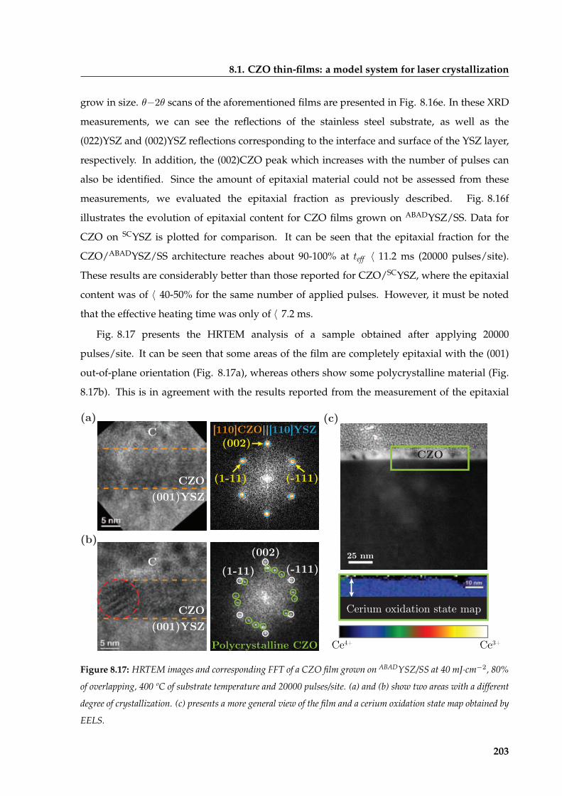
8.1. CZO thin-films: a model system for laser crystallization
grow in size. 2 scans of the aforementioned films are presented in Fig. 8.16e. In these XRD
measurements, we can see the reflections of the stainless steel substrate, as well as the
(022)YSZ and (002)YSZ reflections corresponding to the interface and surface of the YSZ layer,
respectively. In addition, the (002)CZO peak which increases with the number of pulses can
also be identified. Since the amount of epitaxial material could not be assessed from these
measurements, we evaluated the epitaxial fraction as previously described. Fig. 8.16f
illustrates the evolution of epitaxial content for CZO films grown on ABADYSZ/SS. Data for
CZO on SCYSZ is plotted for comparison. It can be seen that the epitaxial fraction for the
CZO/ABADYSZ/SS architecture reaches about 90-100% at teff 〈11.2 ms (20000 pulses/site).
These results are considerably better than those reported for CZO/SCYSZ, where the epitaxial
content was of 〈40-50% for the same number of applied pulses. However, it must be noted
that the effective heating time was only of 〈7.2 ms.
Fig. 8.17 presents the HRTEM analysis of a sample obtained after applying 20000
pulses/site. It can be seen that some areas of the film are completely epitaxial with the (001)
out-of-plane orientation (Fig. 8.17a), whereas others show some polycrystalline material (Fig.
8.17b). This is in agreement with the results reported from the measurement of the epitaxial
(a)
(b)
(001)YSZCZO
C [110]CZO||[110]YSZ(002)
(1-11) (-111)
(001)YSZCZO
C
Polycrystalline CZO
(002)(1-11) (-111)
(c)
Ce4+ Ce3+
Cerium oxidation state map
CZO
25 nm
Figure 8.17: HRTEM images and corresponding FFT of a CZO film grown on ABADYSZ/SS at 40 mJcm2, 80%
of overlapping, 400 ºC of substrate temperature and 20000 pulses/site. (a) and (b) show two areas with a different
degree of crystallization. (c) presents a more general view of the film and a cerium oxidation state map obtained by
EELS.
203

8. Laser-induced crystallization of oxide thin films from CSD precursors
fraction (Fig. 8.16f) which was 〈90-100% for this experimental conditions. In addition, the
CZO film is strained with the ABADYSZ layer as illustrated in the FFT. Despite these films are
highly crystalline, further irradiation could possibly eliminate the remaining polycrystalline
material and crystalline defects enhancing crystallization. Fig. 8.17c depicts a more general
view of the CZO film where an EELS map of the cerium oxidation state has been recorded.
This measurement reveals that the film is only composed of Ce4+ ions, and therefore, neither
Ce3+ nor oxygen vacancies could be identified despite laser annealing was carried out in air
and not in a pure oxygen environment, as it is typically done in thermal treatments.
Despite the simulated longer effective heating time of CZO films on ABADYSZ/SS
compared to CZO on SCYSZ (Fig. 8.15) leads to equivalent processing times with a shorter
number of pulses, it is worth mentioning that the characteristic time θ for this technological
architecture extracted from data fitting in Fig. 8.16f is slightly shorter than the one reported
for single crystal substrates, 4.3 and 7.7 ms respectively. This derives in a slightly larger
effective diffusion coefficient DCZO;Tapelaser;epi 〈2:31014 m2s1 compared to DCZO;SC
laser;epi 〈1:31014
m2s1. Remember that these values have been calculated using Eq. 3.23 with a thickness of
20 nm and the extracted characteristic times.
As we mentioned in section 8.1.2, we can calculate the epitaxial growth rate of CZO films
on ABADYSZ/SS by deriving the fitting function in Fig. 8.16f. Figs. 8.18a and b present the
dependence of the epitaxial growth rate with time and normalized thickness, respectively, for
(a) (b)
CZO/ABADYSZ/SS
CZO/SCYSZ
0.00 0.25 0.50 0.75 1.00Normalized thickness
0 5 10 15 20Effective time (ms)
010002000300040005000
Epita
xial
gro
wth
rate
(nm
·s-1) CZO/ABADYSZ/SS
CZO/SCYSZ
Figure 8.18: Dependence of the epitaxial growth rate of CZO on ABADYSZ/SS with (a) the effective heating time,
and (b) normalized film thickness after laser irradiation at 40 mJcm2 and 400 ºC of substrate temperature. The
data in red corresponds to CZO films on SCYSZ obtained at the same experimental conditions and is plotted for
comparison. Growth rates are extracted by deriving the fitting functions in Fig. 8.16f. Thickness normalization
has been done dividing by the maximum thickness values reported before in sections 5.1 and 5.3.3.
204

8.2. Laser crystallization of multicomponent oxides
samples irradiated at 40 mJcm2 and 400 ºC of substrate temperature. Data for CZO on SCYSZ
obtained at the same experimental conditions is plotted for comparison. Essentially, the initial
epitaxial growth rate of CZOABADYSZ/SS is around two times larger than that of CZO/SCYSZ
(4500 nms1 as compared to 2500 nms1). In addition, it diminishes with the effective heating
time because less material is available for its conversion as epitaxy advances, as we indicated
previously. Again, notice the linear decrease of the epitaxial growth rate with the epitaxial film
thickness.
In either way, full epitaxial film growth is obtained with a lower number of accumulated
pulses than laser annealing of CZO on SCYSZ and, thus, shorter processing time. Apparently,
the degree of epitaxial crystallization and growth rate is somewhat larger for CZO onABADYSZ at initial effective heating times, and it is slightly smaller after 〈5 ms. The reason of
this behavior is that CZO films on ABADYSZ reach epitaxy much faster than on SCYSZ, as
evidenced from the diminishing dependence in the epitaxial growth rate as a function of the
final epitaxial film thickness (Fig. 8.18b). We propose that additional mechanisms like
photoactive defects at the ABADYSZ/SS interface or roughness driven laser-scattering not
considered in the numerical simulations could help increasing peak temperatures and
temperature gradients [125]. Furthermore, it is known that defective materials present lower
thermal conductivities than single crystals due to phonon scattering at defects [266],
contributing to the aforementioned phenomenon. All these additional mechanisms would
promote even higher epitaxial growth in CZO/ABADYSZ than in CZO/SCYSZ. Supplementary
investigations should be carried out in order to validate this hypothesis.
8.2 Laser crystallization of multicomponent oxides
All the work performed in the epitaxial crystallization of CZO films by pulsed laser annealing
provided a better understanding of the mechanisms involved in this growth process, allowing
us to go beyond the knowledge available until now. In addition, it has been crucial to develop
a methodology extensible to the growth of more complex multicomponent oxide thin films.
Particularly in this section, we will investigate the laser crystallization of the following
heterostructures: LaNiO3 (LNO) on (001)SrTiO3 (STO), Ba0:8Sr0:2TiO3 (BST) on
(001)LNO/(001)LaAlO3 (LAO) and La0:7Sr0:3MnO3 (LSMO) on (001)STO.
These oxides where chosen due to their outstanding functional properties already
described in chapter 1. Summarizing, LNO is typically employed as a bottom electrode due to
205

8. Laser-induced crystallization of oxide thin films from CSD precursors
its remarkable electrical conductivity [24], while BST with a Ba/Sr content of 0.8/0.2 is a
ferroelectric/piezoelectric material at room temperature [26–28]. Finally, LSMO with a La/Sr
content of 0.7/0.3 has been employed because it is a metallic and highly ferromagnetic oxide
at room temperature, and lately its interest has been extended to the field of non-volatile
random access memories (NVRAM) [33–35].
It must be noted that growth of BST films has been done on LAO substrates coated with a
CSD-grown LNO film (700 ºC, 10 ºCmin1, 1 h in O2). The main reasons for this choice are that
the use of a bottom electrode is often mandatory in some applications, and LNO is the optimal
candidate while keeping a high chemical and structural compatibility with BST (perovskite
on perovskite) and a relatively low theoretical compressive mismatch ("〈3:6%). In addition,
unlike thermal treatments, high substrate absorption is often required to obtain high enough
crystallization temperatures (section 6.3.2.2). In particular, the very low optical absorption of
LAO substrates (Table. 6.1) could strongly complicate crystallization or even impede it.
8.2.1 Evaluation of experimental conditions, surface morphology and epitaxial
evolution
The thin films described are assumed to be amorphous after decomposition treatments with
CTA at 350 ºC for 30 min (LNO), 450 ºC for 10 min (BST) and 300 ºC for 10 min (LSMO) with
thicknesses around 40-50 nm measured by X-ray reflectometry. The reader is referred to
sections 5.3.1 and A.3.1 for additional information about these results.
It could be assumed that these oxide films are mainly composed of La-O and Ni-O bonds
for LNO, Ba-O, Sr-O and Ti-O bonds for BST, and La-O, Sr-O and Mn-O bonds for LSMO.
Dissociation energies for La-O, Ba-O and Ti-O bonds, reported in Table 8.2, are well above the
Table 8.2: Dissociation energy of the chemical bonds present in LNO, BST and LSMO thin-films. Data extracted
from [296].
Chemical bond Dissociation energy (kJmol1)
La-O 799 (〈8.3 eVbond1)
Ni-O 392 (〈4.1 eVbond1)
Ba-O 563 (〈5.8 eVbond1)
Sr-O 454 (〈4.7 eVbond1)
Ti-O 662 (〈6.9 eVbond1)
Mn-O 402 (〈4.2 eVbond1)
206

8.2. Laser crystallization of multicomponent oxides
photon energy of the Nd:YAG laser (〈4.7 eV at 266 nm). Notice that these energies are for
atomic bonds and may change depending on the electronic environment. However, Ni-O,
Sr-O and Mn-O bonds, as well as the bonds in crystalline defects, present energies similar or
below the laser-photon energy (Table 8.2). Unlike CZO films, this could suggest that
photochemical processes may have an important contribution to crystallization due to direct
photo-induced bond breaking. Despite that, evaluation of the photochemical mechanisms is
rather complex and out of the scope of this thesis due to unknown quantities such as precise
excitation/relaxation times, density of excited and relaxed species, etc [125]. Thus, we will
only simulate the temperature profiles due to photothermal mechanisms, but knowing that
the achieved effects in each system are likely to be highly modified by
photochemically-induced processes.
As we described in Chapter 6, temperature simulations were carried out using the
thermo-physical and optical properties of the materials present in each heterostructure (Table
6.1). The optical properties (n, η, and l) of the decomposed films, depicted in Fig. 8.19,
have been obtained from transmittance and reflectance spectra of films deposited on -Al2O3
substrates and following the methodology explained in section A.4.2. We can see from Fig.
8.19a that transmittance increases with the wavelength from 〈20 to 80%, while the reflectance
(a) (b) (c)
(d) (e) (f)
0
20
40
60
80
100
Tra
nsm
ittan
ce (
%)
200 400 600 800Wavelength (nm)
LNO
BST
LSMO
0
5
10
15
20
Ref
lect
ance
(%
)
200 400 600 800Wavelength (nm)
LNO
BSTLSMO 1.6
2.0
2.4
2.8
Ref
ract
ive
inde
x, n
200 400 600 800Wavelength (nm)
LNO
BSTLSMO
0.10.20.30.40.50.6
Extin
ctio
n co
eff.,
κ
200 400 600 800Wavelength (nm)
LNO
BST
LSMO
0
1
2
3
4
α (1
07 m-1)
200 400 600 800Wavelength (nm)
LNO
BST
LSMO
0
100
200
300
200 400 600 800Wavelength (nm)
l α (
102 n
m)
LNO
BST
LSMO
Figure 8.19: Optical properties of pyrolyzed precursor LNO, BST and LSMO films deposited on -Al2O3
substrates. Measured (a) transmittance and (b) reflectance spectra, calculated (c) refractive index, (d) extinction
coefficient, optical (e) absorption coefficient and (f) penetration depth.
207
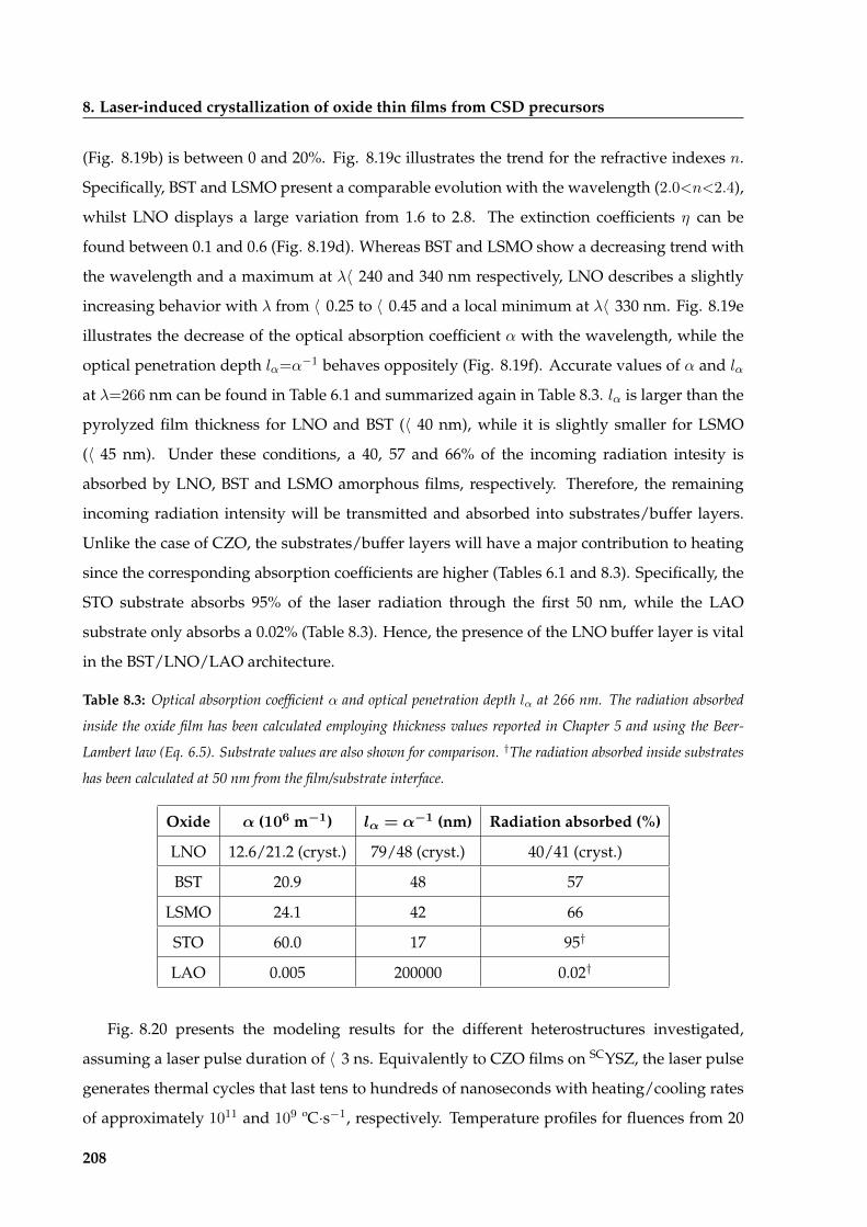
8. Laser-induced crystallization of oxide thin films from CSD precursors
(Fig. 8.19b) is between 0 and 20%. Fig. 8.19c illustrates the trend for the refractive indexes n.
Specifically, BST and LSMO present a comparable evolution with the wavelength (2:0<n<2:4),
whilst LNO displays a large variation from 1.6 to 2.8. The extinction coefficients η can be
found between 0.1 and 0.6 (Fig. 8.19d). Whereas BST and LSMO show a decreasing trend with
the wavelength and a maximum at λ〈240 and 340 nm respectively, LNO describes a slightly
increasing behavior with λ from 〈0.25 to 〈0.45 and a local minimum at λ〈330 nm. Fig. 8.19e
illustrates the decrease of the optical absorption coefficient with the wavelength, while the
optical penetration depth l=1 behaves oppositely (Fig. 8.19f). Accurate values of and l
at λ=266 nm can be found in Table 6.1 and summarized again in Table 8.3. l is larger than the
pyrolyzed film thickness for LNO and BST (〈40 nm), while it is slightly smaller for LSMO
(〈45 nm). Under these conditions, a 40, 57 and 66% of the incoming radiation intesity is
absorbed by LNO, BST and LSMO amorphous films, respectively. Therefore, the remaining
incoming radiation intensity will be transmitted and absorbed into substrates/buffer layers.
Unlike the case of CZO, the substrates/buffer layers will have a major contribution to heating
since the corresponding absorption coefficients are higher (Tables 6.1 and 8.3). Specifically, the
STO substrate absorbs 95% of the laser radiation through the first 50 nm, while the LAO
substrate only absorbs a 0.02% (Table 8.3). Hence, the presence of the LNO buffer layer is vital
in the BST/LNO/LAO architecture.
Table 8.3: Optical absorption coefficient and optical penetration depth lα at 266 nm. The radiation absorbed
inside the oxide film has been calculated employing thickness values reported in Chapter 5 and using the Beer-
Lambert law (Eq. 6.5). Substrate values are also shown for comparison. yThe radiation absorbed inside substrates
has been calculated at 50 nm from the film/substrate interface.
Oxide α (106 m1) lα = α1 (nm) Radiation absorbed (%)
LNO 12.6/21.2 (cryst.) 79/48 (cryst.) 40/41 (cryst.)
BST 20.9 48 57
LSMO 24.1 42 66
STO 60.0 17 95y
LAO 0.005 200000 0.02y
Fig. 8.20 presents the modeling results for the different heterostructures investigated,
assuming a laser pulse duration of 〈3 ns. Equivalently to CZO films on SCYSZ, the laser pulse
generates thermal cycles that last tens to hundreds of nanoseconds with heating/cooling rates
of approximately 1011 and 109 ºCs1, respectively. Temperature profiles for fluences from 20
208

8.2. Laser crystallization of multicomponent oxides
400
600
800
1000
1200
T
empe
ratu
re (
ºC)
0.1 1 10 100 1000Time (ns)
20 mJ·cm-2
30 mJ·cm-2
40 mJ·cm-2
Laserpulse
(d)
(a) (b)
(c)
LNO/STO
400600800
1000120014001600
Tem
pera
ture
(ºC
)
0.1 1 10 100 1000Time (ns)
20 mJ·cm-2
30 mJ·cm-240 mJ·cm-2
Laserpulse
LSMO/STO
LNO/STO
BST/LNO/LAO
LSMO/STO
Tmp=1450 ºC
20 30 400
15
30
45
60
75
Effe
ctiv
e he
atin
gtim
e, t e
ff (n
s)
Fluence (mJ·cm-2)
CZO/YSZ
600750900
1050120013501500
Tem
pera
ture
(ºC
)
20 30 40Fluence (mJ·cm-2)
LNO/STO
LSMO/STO
BST/LNO/LAO
Figure 8.20: Thermal profiles of 40 nm-thick (a) LNO and (b) LSMO films on STO substrates for fluences of 20
mJ· cm−2 (—), 30 mJ· cm−2 (—) and 40 mJ· cm−2 (—) and the substrate at 400 ºC. The solid and dashed lines
are representative of surface and interface profiles, respectively. The laser pulse (—) is plotted as a reference. (c)
Dependence of surface and interface temperatures, and (d) the effective heating time with the laser fluence for the
different heterostructures. The colored areas in (c) indicate the range of temperatures between surface and interface.
to 40 mJ· cm−2, at a substrate temperature of 400 ºC, and after applying a single pulse show
that peak temperatures increase with the laser fluence, as it was expected. More precisely, Fig.
8.20c shows that the maximum temperatures for LNO on STO go from 750 to 1150 ºC, and the
surface/interface temperature difference is up most of few tens of degrees. It must be noted
that LNO suffers a phase transition from LaNiO3 to La2NiO4 at ∼825 ºC [196], and thus, the
use of fluences below that temperature would be advisable. However, we will show later that
such transition was not observed a priori in laser annealed films. Temperatures reached in this
heterostructure are well below the melting point of La2NiO4 (∼1680 ºC). Secondly, a similar
range of temperatures is obtained for BST on LNO/LAO, i. e. maximum temperatures from
800 to 1200 ºC, which are also below the melting point of BST (∼1625 ºC). However, the
temperature variation between surface and interface is much larger than those calculated for
LNO/STO (∼200-300 ºC). In third place, the temperature profiles for LSMO films on STO. In
209

8. Laser-induced crystallization of oxide thin films from CSD precursors
this case, peak temperatures go from 1000 to 1500 ºC and the surface/interface difference is
between 200-400 ºC. It is important to notice that the melting point of LSMO (〈1450 ºC) is
surpassed for fluences close to 40 mJcm2 and, hence, the range of fluences will be restricted
to 20 and 30 mJcm2 for this particular case. Finally, Fig. 8.20d confirms that the effective
heating time teff for the different heterostructures increases with the fluence as previously
indicated for CZO films. These values are significantly smaller than tCZOeff . Additionally, peak
temperatures developed at these fluences are around 200-500 ºC higher than those used in
thermal treatments (700 ºC for LNO, 900 ºC for BST and 900-1000 ºC for LSMO) without
considering photochemical mechanisms which would further increase the recrystallization
rate.
Pulsed laser annealing was performed on LNO, BST and LSMO films at equivalent
experimental conditions to those optimized for CZO films, i. e. using an 80% of beam
overlapping and a substrate temperature of 400 ºC. Fluences employed for each particular
case were 30 mJcm2 (LNO and LSMO) and 40 mJcm2 (BST). Fig. 8.21 shows the surface
morphology of films pyrolyzed using CTA and after the application of 2500, 10000 and 20000
pulses/site. The surface morphology of films after decomposition is rather flat with RMS
roughness of 〈0.3-0.4 nm. However, films develop groove-like structures with sizes of
〈200300 nm in all our cases, also known as ripples or LIPSS (laser-induced periodic surface
structures), after laser irradiation and the RMS roughness rises substantially with the number
of pulses. The formation of ripples is a widely extended phenomenon on laser treatments of
surface materials and occurs within a specific range of parameters that depend on each
material [125, 303, 304, and references therein]. Although ripple formation is still under
investigation, several origins have been proposed such as the interference between incident
and reflected/refracted laser beams or due to excitation of surface electromagnetic waves
(SEW) in conductive materials by the electromagnetic field of the laser [125, and references
therein]. In our case, ripple formation have been only observed in LNO, BST and LSMO films
having some degree of electrical conductivity and not in CZO films which are insulating,
which could point to SEW mechanisms as the main contribution to ripples’ formation.
Nevertheless, the study of laser-induced periodic surface structures has not been assessed in
this thesis.
XRD measurements of the laser-crystallized films described before are presented in Fig.
8.22. In all cases, they grow epitaxially on top of their respective substrates and the intensity of
the (002) reflection seems to increase with the number of pulses as it has been reported for CZO
210

8.2. Laser crystallization of multicomponent oxides
0.5 µm 0.5 µmRMS=2.9 nm
RMS=3.4 nm
RMS=4.0 nm
(c)
(a)
RMS=2.3 nm
RMS=2.9 nm
RMS=4.8 nm
LNO/STO (30 mJ·cm-2)
0.5 µmRMS=8.5 nm
RMS=10.6 nm
RMS=13.9 nm
(b)
2500 pulses 10000 pulses 20000 pulses
2500 pulses 10000 pulses 20000 pulses
2500 pulses 10000 pulses 20000 pulses
BST/LNO/LAO (40 mJ·cm-2)
LSMO/STO (30 mJ·cm-2)
0.25 µmRMS=0.4 nm
Pyrolyzed at350 ºC, 30 min
0.25 µmRMS=0.3 nm
Pyrolyzed at450 ºC, 10 min
0.25 µm
Pyrolyzed at300 ºC, 10 min
RMS=0.3 nm
Figure 8.21: AFM images illustrating the surface morphology of different furnace pyrolyzed and laser-crystallized
oxide heterostructures with 80% of overlapping and 400 ºC of substrate temperature and applying 2500, 10000 and
20000 pulses/site. (a) LNO thin-films on STO irradiated at 30 mJcm2, (b) BST films on LNO/LAO irradiated
at 40 mJcm2 and (c) LSMO thin-films on STO irradiated at 30 mJcm2.
films. A small peak corresponding to the polycrystalline (011) orientation might be present at
〈32º when applying a low number of pulses. The accurate evaluation of the epitaxial fraction
is illustrated in Fig. 8.23, where we present the epitaxial fraction evolution with the effective
heating time for films irradiated at 30 mJcm2 (LNO and LSMO) or 40 mJcm2 (BST), 80%
of overlapping and a substrate temperature of 400 ºC. Data is obtained from 2D-XRD images
equivalent to those presented in Figs. 8.23b,d and f, employing the methodology described in
section A.3.1. It can be observed that the degree of epitaxy for each heterostructure increases
with teff and the system reaches full epitaxy after few milliseconds, i. e. between 1.3 and 2.4
ms depending on the oxide heterostructure. These results are one order of magnitude faster
than those reported for CZO on SCYSZ where we estimated that 〈140000 pulses/site (〈50
ms) would be required to obtain completely epitaxial films. In addition and as we mentioned
before, it should be noted that epitaxial laser crystallization is remarkably faster than the one
211

8. Laser-induced crystallization of oxide thin films from CSD precursors
(a) (b)
(c)
30 35 40 45 50 55
Inte
nsity
(a.
u.)
-2 (º)
102
104
1
108
STO kβ
(011)LNO (002)STO(002)LNO
106
30 mJ/cm2
4h (CTA)
20000 pulses
10000 pulses
2500 pulses
30 35 40 45 50 55
Inte
nsity
(a.
u.)
-2 (º)
102
104
1
108
LAO kβ4h (CTA)
(011)BST
(002)LAO(002)LNO
106
40 mJ/cm2
20000 pulses
10000 pulses
2500 pulses
(002)BST
30 35 40 45 50 55
Inte
nsity
(a.
u.)
-2 (º)
102
104
1
108
STO kβ(011)LSMO
(002)STO(002)LSMO
106
30 mJ/cm2
1h (CTA)
20000 pulses
10000 pulses
2500 pulses
LNO on STO BST on LNO/LAO
LSMO on STO
Figure 8.22: XRD measurements of the laser-crystallized fims with 80% of overlapping and 400 ºC of substrate
temperature and applying 2500, 10000 and 20000 pulses/site: (a) LNO on STO, (b) BST on LNO/LAO, and
(c) LSMO on STO. A fluence of 30 mJcm2 was used to grow LNO and LSMO films, while BST films were
irradiated at 40 mJcm2. Equivalent samples obtained by CTA after 4 h (LNO and BST) and 1 h (LSMO) are
presented for comparison.
achieved with thermal treatments.
Despite much effort was put to obtain measurable LNO, BST and LSMO TEM samples, we
were only able to study BST specimens due to issues during sample preparation. Fig. 8.24
illustrates HRTEM investigations carried out on a laser annealed BST film on a LAO substrate
coated with LNO at 40 mJcm2, 80% of overlapping, a substrate temperature of 400 ºC after
20000 pulses/site. It can be observed that the highly crystalline and epitaxial CSD-LNO layer
grown on LAO (700 ºC, 10 ºCmin1 for 1 h) provides an optimal template to promote BST
epitaxy, which is in agreement with the results reported from the epitaxial fraction calculation
by XRD. Additionally, Figs. 8.24b and c show that the epitaxial BST and LNO films grow
cube-on-cube with each other and the substrate, i. e. (001)BST[001]k(001)LNO[001] and
(001)LNO[001]k(001)LAO[001]. On the one hand, LNO grows completely strained on LAO
with an in-plane compression of the LNO lattice of -1.6% (aLNObulk =3:851 A and
212
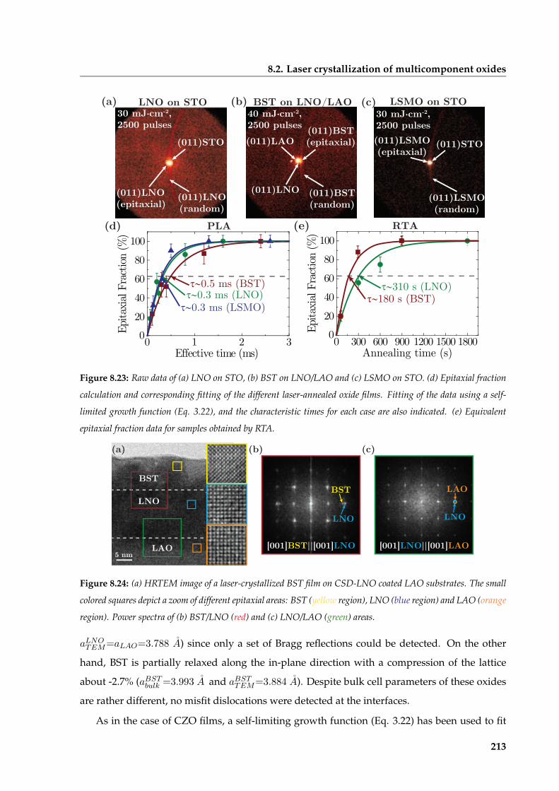
8.2. Laser crystallization of multicomponent oxides
(a) (b)(a)
(011)LNO(random)
(011)LNO(epitaxial)
(011)STO
30 mJ·cm-2,2500 pulses
(c)
(d) (e)
(011)BST(random)
(011)LNO
(011)BST(epitaxial)
40 mJ·cm-2,2500 pulses(011)LAO
(011)LSMO(random)
(011)LSMO(epitaxial)
(011)STO
30 mJ·cm-2,2500 pulses
LNO on STO BST on LNO/LAO
0 1 2 3
Effective time (ms)0
20
40
60
80
100
Epita
xial
Frac
tion
(%)
τ∼0.5 ms (BST)τ∼0.3 ms (LNO)τ∼0.3 ms (LSMO)
LSMO on STO
0 300 600 900 1200 1500 1800
Annealing time (s)0
20
40
60
80
100
Epita
xial
Frac
tion
(%)
τ∼180 s (BST)τ∼310 s (LNO)
PLA RTA
Figure 8.23: Raw data of (a) LNO on STO, (b) BST on LNO/LAO and (c) LSMO on STO. (d) Epitaxial fraction
calculation and corresponding fitting of the different laser-annealed oxide films. Fitting of the data using a self-
limited growth function (Eq. 3.22), and the characteristic times for each case are also indicated. (e) Equivalent
epitaxial fraction data for samples obtained by RTA.
5 nm
LNO
BST
LAO [001]BST||[001]LNO [001]LNO||[001]LAO
(a) (b) (c)
LNO
BST
LNO
LAO
Figure 8.24: (a) HRTEM image of a laser-crystallized BST film on CSD-LNO coated LAO substrates. The small
colored squares depict a zoom of different epitaxial areas: BST (yellow region), LNO (blue region) and LAO (orange
region). Power spectra of (b) BST/LNO (red) and (c) LNO/LAO (green) areas.
aLNOTEM=aLAO=3.788 A) since only a set of Bragg reflections could be detected. On the other
hand, BST is partially relaxed along the in-plane direction with a compression of the lattice
about -2.7% (aBSTbulk =3.993 A and aBSTTEM=3.884 A). Despite bulk cell parameters of these oxides
are rather different, no misfit dislocations were detected at the interfaces.
As in the case of CZO films, a self-limiting growth function (Eq. 3.22) has been used to fit
213

8. Laser-induced crystallization of oxide thin films from CSD precursors
the data in Fig. 8.23 and obtain the characteristic times for epitaxial crystallization by laser
annealing θlaser;epi, which are 0.3 ms (LNO and LSMO) and 0.5 ms (BST). These values of
θlaser;epi are around one order of magnitude shorter than θCZO;SClaser;epi 〈7:7 ms, and between 5 and
6 orders of magnitude as compared to the epitaxial characteristic times for thermal treatments
of equivalent oxides (θthermal;epi〈180310 s) obtained in chapter 5. The diffusion coefficients
of laser epitaxial crystallization have been also calculated from Eq. 3.23, using the
characteristic times and the final epitaxial film thickness (sections 5.1 and A.3.1). The obtained
values of Dlaser;epi are 5.21013, 6.11013 and 7.51013 m2s1 for LNO, BST and LSMO,
respectively. These diffusion coefficients differ around one order of magnitude from
DCZO;SClaser;epi 〈1.31014 m2s1, and between 5 and 6 orders of magnitude from
Dthermal;epi〈5-171019 m2s1 (Chapter 5). We also calculated the epitaxial growth rates
deriving the fitting curve from Fig. 8.23d. Particularly, Fig. 8.25a shows that the epitaxial
growth rate decreases with the effective heating time as reported before for CZO (Fig. 8.18).
Like the diffusion coefficients, the initial epitaxial growth rate values are around one order of
magnitude larger than CZO ones. Fig. 8.25b illustrates an almost linear reduction in the
epitaxial growth rate when normalized to each film final thickness, i. e. 25, 35 and 30 nm for
LNO, BST and LSMO respectively (sections 5.1 and A.3.1).
Previously, it has been mentioned that atomic diffusion in laser annealed CZO films could
be altered by the action of temperature gradients since its temperature dependence could only
explain around 2 of the 4-5 orders of magnitude shorter characteristic time and larger
0.00 0.25 0.50 0.75 1.000
2
4
6
8
10
Epita
xial
gro
wth
rate
(10
4 nm
·s-1)
Normalized thickness
CZO
BSTLNO
LSMO
(a) (b)
0.0 0.5 1.0 1.5 2.0Effective heating time (ms)
0
2
4
6
8
10
Epita
xial
gro
wth
rate
(10
4 nm
·s-1)
CZOBST
LNO
LSMO
Figure 8.25: Dependence of the epitaxial growth rate for different oxide heterostructures with (a) the effective
heating time, and (b) the normalized thickness. They can be obtained by transforming the epitaxial fraction to
thickness Film thickness values are reported in sections 5.1 and A.3.1. Thickness normalization has been done
dividing by the maximum thickness values reported before in sections 5.1 and 5.3.3.
214

8.2. Laser crystallization of multicomponent oxides
diffusion coefficient compared to thermal treatments. Likewise, we propose that the epitaxial
transformation of laser irradiated LNO, BST and LSMO films will be also affected by
temperature gradients accordingly.
Additionally and as we mentioned before, Nakajima et al. indicated that photochemical
processes may influence this fast epitaxial oxide growth [72, 300]. We already pointed out that
photochemical processes may play a vital role in the crystallization of these LNO, BST and
LSMO films since the laser photons have more energy than some metal-oxide bonds present
(Table 8.2). Contrarily, the dissociation energy of bonds in CZO films are almost twice the laser-
photon energy and we proposed that their crystallization is mostly driven by photothermal
mechanisms leading to longer epitaxial characteristic times and smaller diffusion coefficients.
In summary, it seems that LNO, BST and LSMO films crystallization may be driven by both
photothermal and photochemical processes.
The results presented illustrate that laser epitaxial crystallization of pyrolyzed precursor
metal-organic films may be a valid alternative, substituting thermal treatments.
8.2.2 Functional properties of laser crystallized films
Besides the optimization of epitaxial growth and surface morphology, it is of vital importance
to characterize the functional properties of thin-films. Although much effort could be
undertaken in optimizing the laser crystallization of the different oxides to improve their
functional properties, in this thesis we focused on evaluating the best samples produced by
laser annealing and compare them with those obtained using thermal treatments.
Fig. 8.26 depicts the electrical resistivity of LNO films grown by laser treatments (30
mJcm2, 80% of overlapping, a substrate temperature of 400 ºC and applying 20000
pulses/site) and compared with thermally annealed samples (700 ºC for 15 min and 1h).
Although laser-grown LNO films show good metallic behavior within the range reported in
the literature [221, 225, 226], its resistivity is around one order of magnitude higher than that
of thermally crystallized films. The difference in resistivity could be associated to the
particular surface morphology or crystallinity of each sample since the laser treated sample is
rougher than those obtained by thermal treatments. It must also be noted that the effective
heating times in laser treatments are much shorter, 〈360 νs compared to 15 min and 1 h of
thermal annealing. Thus, further optimization of the experimental conditions should provide
resistivities equivalent to pure thermal treatments.
We have also evaluated the local ferroelectric/piezoelectric performance of epitaxially
215

8. Laser-induced crystallization of oxide thin films from CSD precursors
0
500
1000
1500
2000
2500
3000
0 50 100 150 200 250 300
Res
istiv
ity (µΩ
·cm
)
Temperature (K)
RTACTA
PLA
(b)
Figure 8.26: Resistivity measurements for LNO films on STO. Films were grown using laser irradiation at 30
mJcm2, 80% of overlapping, a substrate temperature of 400 ºC and applying 20000 pulses/site (green circles);
RTA at 700 ºC, 20 ºCs1 for 15 min (red circles) and CTA (blue squares) at 700 ºC, 10 ºCmin1 for 1 h in O2.
grown BST films as indicated in section A.4.6. Fig. 8.27 presents a comparison between
piezoresponse force microscopy (PFM) measurements for BST film grown on (001)LNO/LAO
by laser annealing (40 mJcm2, 80% of overlapping, a substrate temperature of 400 ºC and
applying 10000 pulses/site) and thermal treatments (900 ºC for 4 h in O2). Fig. 8.27a shows
two squares of different sizes written at 7 V, indicating that ferroelectric domains were
successfully polarized. Despite both samples display equivalent PFM amplitude versus
sample bias loops (Fig. 8.27b), the hysteresis is slightly better for the sample produced by
thermal annealing; a behavior already expected due to the longer effective heating time, i. e.
〈200 νs and 4 h respectively. Fig. 8.27c presents well-defined and saturated hysteresis loops
of the ferroelectric phase domains with coercive voltages of 〈2-3 V. The piezoelectric
(b) (c)(a)+7 V
-7 V
1 µm
+7 V
-7 V
Thermal
Laser-8 -6 -4 -2 0 2 4 6 8
0.0
0.1
0.2
0.3
Am
plitu
de (
nm)
Sample Bias (V)
ThermalLaser
0306090
120150
180
Phas
e (º
)
-8 -6 -4 -2 0 2 4 6 8Sample Bias (V)
Thermal
Laser
Figure 8.27: Piezoresponse Force Microscopy (PFM) measurements of a BST film annealed at 900 ºC, 20 ºCs1
for 4 h in O2. (a) PFM phase image showing the written domains with a voltage of +7 V (outter square) and -7 V
(inner square). Representative hysteresis loops of (b) amplitude and (c) phase.
216
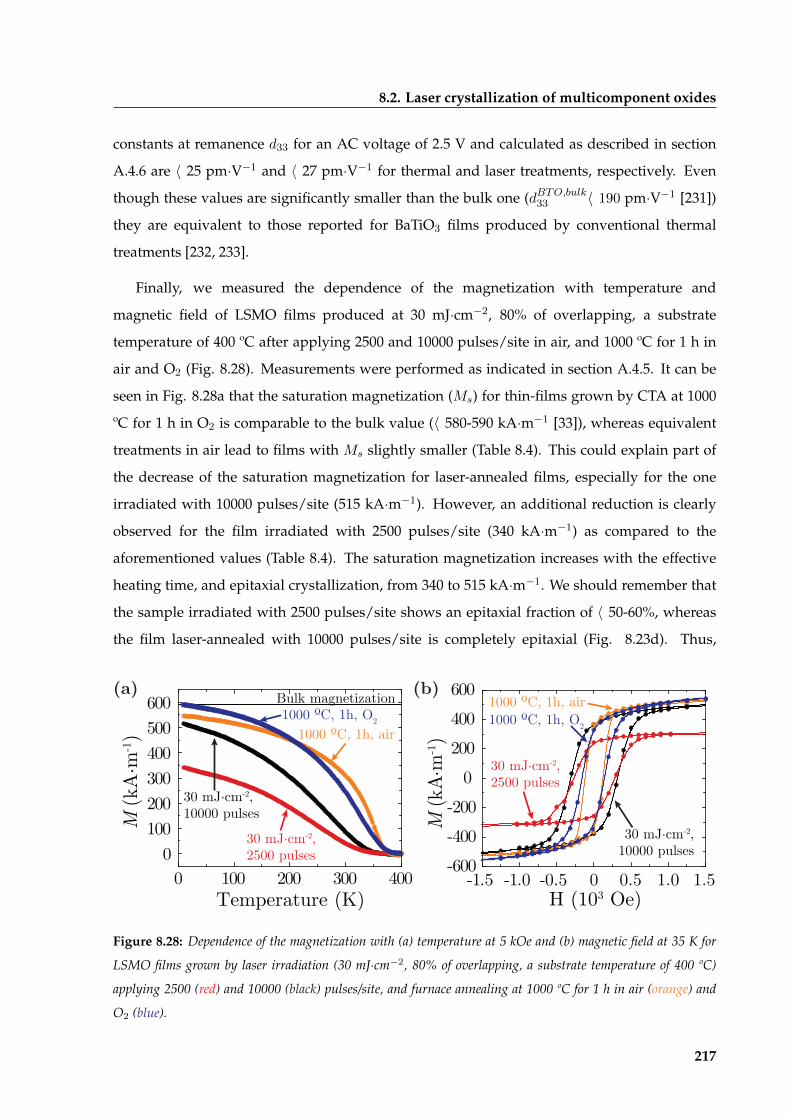
8.2. Laser crystallization of multicomponent oxides
constants at remanence d33 for an AC voltage of 2.5 V and calculated as described in section
A.4.6 are 〈25 pmV1 and 〈27 pmV1 for thermal and laser treatments, respectively. Even
though these values are significantly smaller than the bulk one (dBTO;bulk33 〈190 pmV1 [231])
they are equivalent to those reported for BaTiO3 films produced by conventional thermal
treatments [232, 233].
Finally, we measured the dependence of the magnetization with temperature and
magnetic field of LSMO films produced at 30 mJcm2, 80% of overlapping, a substrate
temperature of 400 ºC after applying 2500 and 10000 pulses/site in air, and 1000 ºC for 1 h in
air and O2 (Fig. 8.28). Measurements were performed as indicated in section A.4.5. It can be
seen in Fig. 8.28a that the saturation magnetization (Ms) for thin-films grown by CTA at 1000
ºC for 1 h in O2 is comparable to the bulk value (〈580-590 kAm1 [33]), whereas equivalent
treatments in air lead to films with Ms slightly smaller (Table 8.4). This could explain part of
the decrease of the saturation magnetization for laser-annealed films, especially for the one
irradiated with 10000 pulses/site (515 kAm1). However, an additional reduction is clearly
observed for the film irradiated with 2500 pulses/site (340 kAm1) as compared to the
aforementioned values (Table 8.4). The saturation magnetization increases with the effective
heating time, and epitaxial crystallization, from 340 to 515 kAm1. We should remember that
the sample irradiated with 2500 pulses/site shows an epitaxial fraction of 〈50-60%, whereas
the film laser-annealed with 10000 pulses/site is completely epitaxial (Fig. 8.23d). Thus,
(b)(a)
0 100 200 300 4000
100200300400500600
M (
kA·m
-1)
Temperature (K)
1000 ºC, 1h, air
30 mJ·cm-2,2500 pulses
Bulk magnetization
30 mJ·cm-2,10000 pulses
1000 ºC, 1h, O2
-1.5 -1.0 -0.5 0 0.5 1.0 1.5-600-400-200
0200400600
M (
kA·m
-1)
H (103 Oe)
1000 ºC, 1h, air
30 mJ·cm-2,2500 pulses
30 mJ·cm-2,10000 pulses
1000 ºC, 1h, O2
Figure 8.28: Dependence of the magnetization with (a) temperature at 5 kOe and (b) magnetic field at 35 K for
LSMO films grown by laser irradiation (30 mJcm2, 80% of overlapping, a substrate temperature of 400 ºC)
applying 2500 (red) and 10000 (black) pulses/site, and furnace annealing at 1000 ºC for 1 h in air (orange) and
O2 (blue).
217
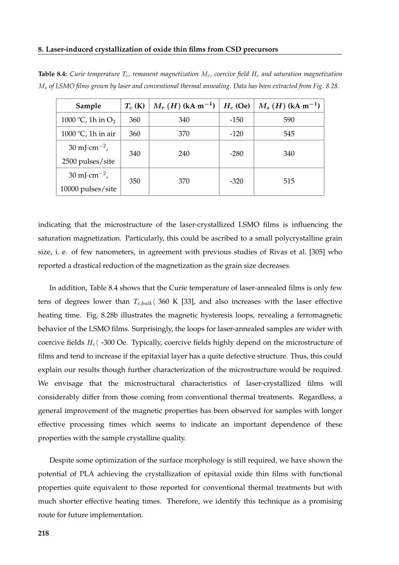
8. Laser-induced crystallization of oxide thin films from CSD precursors
Table 8.4: Curie temperature Tc, remanent magnetization Mr, coercive field Hc and saturation magnetization
Ms of LSMO films grown by laser and conventional thermal annealing. Data has been extracted from Fig. 8.28.
Sample Tc (K) Mr (H) (kAm1) Hc (Oe) Ms (H) (kAm1)
1000 ºC, 1h in O2 360 340 -150 590
1000 ºC, 1h in air 360 370 -120 545
30 mJcm2,
2500 pulses/site340 240 -280 340
30 mJcm2,
10000 pulses/site350 370 -320 515
indicating that the microstructure of the laser-crystallized LSMO films is influencing the
saturation magnetization. Particularly, this could be ascribed to a small polycrystalline grain
size, i. e. of few nanometers, in agreement with previous studies of Rivas et al. [305] who
reported a drastical reduction of the magnetization as the grain size decreases.
In addition, Table 8.4 shows that the Curie temperature of laser-annealed films is only few
tens of degrees lower than Tc;bulk〈360 K [33], and also increases with the laser effective
heating time. Fig. 8.28b illustrates the magnetic hysteresis loops, revealing a ferromagnetic
behavior of the LSMO films. Surprisingly, the loops for laser-annealed samples are wider with
coercive fields Hc〈-300 Oe. Typically, coercive fields highly depend on the microstructure of
films and tend to increase if the epitaxial layer has a quite defective structure. Thus, this could
explain our results though further characterization of the microstructure would be required.
We envisage that the microstructural characteristics of laser-crystallized films will
considerably differ from those coming from conventional thermal treatments. Regardless, a
general improvement of the magnetic properties has been observed for samples with longer
effective processing times which seems to indicate an important dependence of these
properties with the sample crystalline quality.
Despite some optimization of the surface morphology is still required, we have shown the
potential of PLA achieving the crystallization of epitaxial oxide thin films with functional
properties quite equivalent to those reported for conventional thermal treatments but with
much shorter effective heating times. Therefore, we identify this technique as a promising
route for future implementation.
218

8.2. Laser crystallization of multicomponent oxides
8.2.3 Laser crystallization of BST films on technical substrates for electronic
applications
We already mentioned that BST is a widely used oxide in electronic applications due to
multiple electrical and optical properties dependent on composition [26–30]. Although in the
previous section we investigated the epitaxial growth of BST thin-films on single crystal
oxides, the substrate architecture often employed is based on Pt-coated silicon wafers [106].
Recently, LNO-coated silicon has proven to be a reliable alternative provided LNO is an
excellent conductor and has a better compatibility than platinum with BST, i. e. perovskite on
perovskite with similar lattice parameters [24, 25]. A description of the LNO/SiO2/Si
substrate architecture where BST films have been grown can be found in section 2.1.2.2.
The work that will be presented here is a brief summary of the experiments conducted in
the framework of a short-term stay. Our aim was to explore the use of a different laser system
to investigate its effect on crystallization, and compare it with the experiments previously
presented in section 8.2. Particularly, we employed a KrF excimer laser working at 248 nm
wavelength, with a pulse duration of 20-25 ns and a repetition rate of 20 Hz. Despite various
experimental conditions were tested, optimization of the multiple parameters involved was
beyond the scope of this work.
It has been demonstrated in section 6.3.2.1 that a longer laser pulse duration would lead to
temperature profiles with lower maximum temperatures and longer thermal cycles, although
this may depend on the modeled heterostructure. Thus, we must find a combination between
fluence and substrate temperature which result in comparable experimental conditions to those
employed for BST/LNO/LAO at 40 mJcm2 and a substrate temperature of 400 ºC (Fig. 8.20b).
Numerical simulations were performed considering a laser pulse duration of 20 ns and
thermo-physical and optical parameters of the various constituents of the modeled
heterostructure (Table 6.1). The thicknesses of each material employed in the simulations were
40, 150 and 500 nm for BST, LNO and SiO2, respectively, the remaining thickness (100 νm)
corresponds to silicon. Fig. 8.29a depicts the temperature profiles of BST on LNO/SiO2/Si
substrates with a base temperature of 500 ºC and fluences of 50, 65 and 75 mJcm2. Peak
temperatures achieved in the system are of 〈11001450 ºC which leads to heating/cooling
rates up to 〈109 ºCs1. Unlike the thermal cycles developed in previous simulations where
the pulse duration was of 3 ns, the longer temperature profiles which last hundreds to
thousands of nanoseconds result in unappreciable surface/interface temperature variations of
219

8. Laser-induced crystallization of oxide thin films from CSD precursors
(a) (b)
10000400
600
800
1000
1200
1400
Tem
pera
ture
(ºC)
Time (ns)0.1 1 10 100 1000 10000
75 mJ·cm-2
65 mJ·cm-2
50 mJ·cm-2Laser pulse
0.8
0.9
1.0
1.1
50 60 70 80
Effe
ctiv
e he
atin
gtim
e, t e
ff (µ
s)
Fluence (mJ·cm-2)
Figure 8.29: (a) Temperature profiles of 40 nm-thick BST films on LNO-coated SiO2/Si substrates at 500 ºC for
fluences of 50 mJcm2 (—), 65 mJcm2 (—) and 75 mJcm2 (—). The solid and dashed lines are representative
of surface and interface profiles, respectively. The laser pulse (—) is plotted as a reference. (c) Dependence of the
effective heating time with the laser fluence at a substrate temperature of 500 ºC.
only tens of degrees. Hence, the temperature gradients will be also smaller, i. e. 〈108109
ºCm1. Furthermore, Fig. 8.29b illustrates that the effective heating time teff increases with the
fluence like in previous simulations, but it is around 2-3 orders of magnitude longer (6-20 ns
compared to 800-1100 ns). Such difference is caused by the longer pulse duration. It must be
remembered that teff has been calculated from simulated temperatures above 600 ºC.
Laser annealing experiments of BST films on LNO/SiO2/Si substrates were done at a
fluence of 65 mJcm2, and a substrate temperature of 500 ºC since the peak temperature
reached is equivalent to the one simulated for BST on LNO/LAO with the Nd:YAG laser (Fig.
8.20b). In this case, no overlapping of pulses was needed because the KrF excimer laser beam
has a top-hat spatial distribution and the beam is larger than the sample size, i. e.
approximately 21 cm2 compared to 0.50.5 cm2. Figs. 8.30a and b show the surface
morphology after accumulating 12000 and 72000 pulses, respectively. It can be seen that films
are quite granular with sizes around 100 nm, and a large amount of pores with similar sizes.
Areas with resonant morphology (ripple-like) are also observed. The RMS roughness is
comparable to that reported for epitaxial BST films using the Nd:YAG laser, and also increases
with the number of pulses from 5.2 to 6.9 nm.
XRD measurements presented in Fig. 8.30c illustrate the presence of (00l) epitaxial and
(011) polycrystalline orientations of BST and LNO. More specifically, Fig. 8.30d indicates that
both BST and LNO films have a high tendency to be uniaxial. The degree of crystallization
increases with the number of pulses as expected. Equivalent experiments and
220

8.2. Laser crystallization of multicomponent oxides
50 mJ/cm2,12000 pulses
(a) (c)65 mJ·cm-2,12000 pulses
75 mJ/cm2,12000 pulses
(b) 65 mJ·cm-2,72000 pulses
RMS=5.2 nm
RMS=6.9 nm
20 30 40 50 60 70 80
θ-2θ (º)
(002)
1
102
Inte
nsity
(a.
u.)
Si kβ(011)104
106(004)Si
12000pulses
72000pulses
(011)(002)
65 mJ·cm-2
(001)(001)
LNO/Si
(d) 72000 pulses
(002)
(002)
BST/LNO
(011)(001)
(011) (001)
Figure 8.30: AFM images of 40 nm-thick BST films on LNO/SiO2/Si substrates grown with a KrF laser at 65
mJ· cm−2, a substrate temperature of 500 ºC, and applying (a) 12000 and (b) 72000 pulses. (c) XRD measurements
of BST films irradiated at 65 mJ· cm−2 after applying 12000 (—) and 72000 (—) pulses. The LNO-coated silicon
substrate (—) is plotted for comparison. The reflections corresponding to the BST and LNO films are indicated
in red and green, respectively. (d) 2D-XRD image of a BST film irradiated at 65 mJ· cm−2 after applying 72000
pulses.
characterizations where done at fluences of 50 and 75 mJ· cm−2, showing rather similar surface
morphology and crystallinity.
Conventionally, the strategy followed for the fabrication of BST devices involves the
deposition of multiple layers until thicknesses above 150 nm are achieved [26, 28]. Thus, we
evaluated and compared the laser crystallization of BST films with different thicknesses. The
methodology employed to produce thicker films consisted of several deposition steps
followed by a pyrolysis treatment at 450 ºC for 10 min as detailed in Chapters 2 and 5.
In Figs. 8.31a and b, we show that the resulting surface morphology of 40 nm- and 160 nm-
thick, 1 and 4 pyrolysis respectively, BST films grown by laser annealing at 65 mJ· cm−2, 500
ºC and accumulating 72000 pulses is significantly different. The former case presents a highly
homogeneous surface with grains of 100 nm and a RMS roughness of 6.9 nm (Fig. 8.30b), while
the later reveals grain domains with sizes larger than 1 µ m, a RMS roughness of 18.9 nm, and
the appearance of structures resembling to cracks. The multiple origins of crack formation will
be discussed later. Fig. 8.31c presents the XRD spectra comparing BST films with thicknesses of
40 and 160 nm. It is clearly seen that these films grow randomly oriented with a certain degree
of uniaxiality as we mentioned before. In addition, the degree of crystallization seems to be
substantially higher for thicker films since the different BST reflections are much more intense.
221

8. Laser-induced crystallization of oxide thin films from CSD precursors
(c)40 nm
RMS=6.9 nm
20 30 40 50 60 70 80
θ-2θ (º)
(002)
1
102In
tens
ity (
a.u.
)
Si kβ(011)104
106 (004)Si
40 nm
160 nm
(011)(002)
65 mJ/cm2,72000 pulses
(001)
(001)
(a)
1 µm
(b) 160 nm
RMS=18.9 nm
Figure 8.31: Scanning Electron Microscopy (SEM) images of (a) 40 nm- and (b) 160 nm-thick BST films on
LNO/SiO2/Si substrates grown with a KrF laser at 65 mJ· cm−2, a substrate temperature of 500 ºC, and applying
72000 pulses. (c) XRD measurements of BST films with thicknesses of 40 nm (—) and 160 nm (—) irradiated at
65 mJ· cm−2 after applying 72000 pulses. The reflections corresponding to the BST and LNO films are indicated
in red and green, respectively.
A deeper investigation of BST films with different thicknesses irradiated by laser at 65
mJ· cm−2, 500 ºC of substrate temperature and 12000 pulses has been performed by HRTEM.
On the one hand, Fig. 8.32a depicts a 40 nm-thick film which is composed by
randomly-oriented nanoparticles although XRD indicated a tendency towards uniaxiality. On
the other hand, TEM analysis of a thicker BST film (Fig. 8.32b) unveils a partially crystallized
BST film with a thickness of ∼160 nm. Interestingly, a polycrystalline region of 50-70 nm has
been detected close to the film surface as illustrated in the power spectrum from the blue
region. The remaining film thickness, closer to the interface with LNO, has been found to be
entirely amorphous as it can be observed in the zoomed orange region.
Laser radiation is absorbed from the surface, and thus, heat propagates from there into the
heterostructure (section 6.3.2). Moreover, the heating process is highly dependent on the
optical penetration depth which for BST is ∼36 nm at λ∼248 nm, i. e. a 63% of the incoming
radiation is absorbed through that thickness. Consequently, the film thickness will become
highly important during the heating process. Simulated temperature profiles for BST films
with thicknesses of 40 and 160 nm grown on LNO/SiO2/Si substrates (Fig. 8.33) illustrate that
equivalent peak temperatures and effective heating times are obtained in both
heterostructures. Although the difference in temperatures between surface and interface ∆T
222

8.2. Laser crystallization of multicomponent oxides
(a)
(b)
LNO
SiO2
BST
150 nm 10 nmLNO
Amorphous BST
10 nm
Polycryst.BST
[111]BST
(-110)
(0-11)
LNO
40 nm
BST
SiO2
(001)
[001]BST
Figure 8.32: HRTEM characterization of BST films grown on LNO/SiO2/Si substrates at 65 mJ· cm−2, 500 ºC of
substrate temperature and 12000 pulses with thicknesses of (a) 40 nm and (b) 160 nm.
(a) (b)
400
600
800
1000
1200
1400
Tem
pera
ture
(ºC)
Time (ns)0.1 1 10 100 1000 10000
160 nm40 nm
0 200 400 600400
600
800
1000
1200
1400
Tem
pera
ture
(ºC)
Thickness (nm)
LNO
SiO2/Si
BST
LNO
SiO2/Si
0 200 400 600Thickness (nm)
BST
40 nm BST 160 nm BST
Figure 8.33: Temperature profiles of BST films with thicknesses of 40 and 160 nm grown on LNO-coated SiO2/Si
substrates. (a) Time and (b) thickness dependence of temperature for a fluence of 65 mJ· cm−2 and a substrate
temperature of 500 ºC. The solid and dashed lines in (a) are representative of surface and interface profiles,
respectively.
223

8. Laser-induced crystallization of oxide thin films from CSD precursors
are ∼50 ºC and ∼300 ºC for films with thicknesses of 40 and 160 nm, respectively, it leads to
similar temperature gradients of ∼109 ºC· m−1. However, the actual temperature near the
interface for the 160 nm film is only of ∼1000 ºC, suggesting that this temperature is probably
too low to induce proper laser crystallization, and thus, the material at the processing
conditions employed would be kept amorphous. In fact, this would be consistent with the
observation that the crystallization of 40 nm-thick films at lower fluences (50 mJ· cm−2, which
is equivalent to ∼1100 ºC) is dramatically reduced.
8.2.3.1 Crack formation in thick BST films crystallized by PLA
It has been mentioned before that cracks may appear for thick BST films after laser treatments
(Fig. 8.31b). In Fig. 8.34, we present a HRTEM image of a BST film with a thickness of 160 nm
after laser annealing at 65 mJ· cm−2, a substrate temperature of 500 ºC and 12000 pulses. There,
a crack-like structure reaching the SiO2 film can be detected.
SiO2
LNO
Si
BST
0.5 µm
Figure 8.34: HRTEM image of a BST film on LNO/SiO2/Si illustrating a crack.
Essentially, cracks may be caused by the difference in thermal expansion coefficients
(TECs) of the multiple oxides, as well as the densification process occurring during
crystallization. Indeed, Table 8.5 reveals that although the thermal expansion coefficients of
BST and LNO are quite different (12.9· 10−6 K−1 and 8.2· 10−6 K−1), they differ to a great extent
from that of SiO2 (0.5· 10−6 K−1), and thus, this may lead to the formation of cracks. In
addition, temperature simulations shown in Fig. 8.33 also indicate a temperature difference
between surface and interface of ∼300 ºC for films with a thickness of 160 nm. Consequently,
the temperature gradient coupled with the different degree of crystallization between the
film’s surface and interface, i. e. the film is polycrystalline at the surface and amorphous at the
interface (Fig. 8.32b), may also induced film cracking.
Likewise, the appearance of cracks is a phenomenon that has also been reported by Baldus
et al. in laser crystallized BST films on Pt/SiO2/Si substrates [307]. They observed that cracks
224

8.3. Summary and conclusions
Table 8.5: Thermal expansion coefficients (TECs or ) of the materials present in the BST/LNO/SiO2/Si
heterostructure. Data extracted from [215, 218, 306].
Oxide η (106 K1)
BST 12.9
LNO 8.2
SiO2 0.5
Si 2.6
appear in films with thicknesses above 130 nm and hypothesize that their origin lies in the
stress caused in the film due to inhomogeneous heating, as well as film densification. Finally,
we propose that a multilayered laser growth strategy should be followed in order to avoid
large temperature gradients and film densification, and thus, reduce the formation of cracks.
8.3 Summary and conclusions
In this chapter, we investigated the crystallization of various oxide thin-films by pulsed laser
annealing in air of pyrolyzed metal-organic precursor films. Firstly, we evaluated the epitaxial
growth of CZO thin-films on SCYSZ substrates as a model system to crystallize more complex
oxide heterostructures. In particular, we determined the influence of different experimental
parameters on crystallization such as laser fluence, substrate temperature, degree of beam
overlapping and number of laser pulses. Essentially, crystallization increases with the
aforementioned parameters and it is possible to obtain a good degree of epitaxy. The
overlapping of laser pulses was required to homogenize irradiation since the laser employed
has a nearly gaussian spatial distribution.
Modeling of the temperatures developed in the system reveals that the origin of such
improvement in crystallization is caused by higher maximum temperatures and longer
thermal pulses as fluence and substrate temperature increase. Despite it is possible to achieve
melting and recrystallization of CZO at fluences of 〈80 mJcm2, the surface develops
molten-induced rounded structures which increase the RMS roughness above 4 nm, which is
too high for some applications. Therefore, we have chosen a set of experimental conditions in
order to perform solid state crystallization (40 mJcm2, substrate at 400 ºC and 80% of
overlapping), obtaining a smoother surface with RMS roughness below 1 nm. Under these
conditions, the epitaxial growth of CZO has been investigated by increasing the number of
225

8. Laser-induced crystallization of oxide thin films from CSD precursors
pulses/site and showing that 〈50% of epitaxy is achieved after 7.2 ms of effective heating
(20000 pulses/site) and around 50 ms (140000 pulses/site) would be required to obtain a
completely epitaxial film with the laser employed in this work. Remarkably, we have proven
that epitaxial crystallization derived from laser treatments, which lasts tens of milliseconds, is
orders of magnitude faster than in thermal annealing where heating times are of tens of
minutes. In turn, this also leads to epitaxial growth rates 4-5 orders of magnitude larger. We
propose that photothermal mechanisms are most likely the main source of such fast growth
because the metal-oxide bonds have higher energy than the laser photons. Specifically, we
envisage that the higher temperatures achieved during laser treatments, as well as the large
temperature gradients developed in laser-annealed films could boost atomic diffusion orders
of magnitude, enhancing crystallization and epitaxial growth as compared to thermal
treatments. Regardless, photochemical processes may also assist the temperature rise since
they could be particularly strong at crystalline defects.
A similar solid-state crystallization behavior has been found for CZO films onABADYSZ/SS metallic substrates. However, the epitaxial growth has proven to be slightly
faster, i. e. a 〈90-100% of epitaxy is achieved after 11.2 ms of effective heating (20000
pulses/site), while we predicted that 〈50 ms would be needed for CZO films on SCYSZ to
reach full epitaxy. This behavior was mainly attributed to the larger optical absorption ofABADYSZ at the laser wavelength as compared to SCYSZ due to the presence of crystalline
defects.
Crystallization of multicomponent oxide heterostructures such as LNO/STO,
BST/LNO/LAO and LSMO/STO has also been performed employing equivalent
experimental conditions to those of CZO films. Completely epitaxial films were grown after
2-4 ms of effective heating (20000 pulses/site). Besides photothermal mechanisms, we cannot
neglect that photochemical processes have a larger influence in the crystallization of these
oxides because some metal-oxide bonds have dissociation energies lower than the laser
photon. In this case, the surface morphology was characterized by the presence of groove-like
structures known as ripples, which lead to larger RMS roughness of 2-14 nm. Modification of
the laser beam polarization should possibly allow to eliminate these structures.
The functional characterization of laser annealed films revealed very interesting results
when compared with thermal treatments. In first place, the electrical resistivity of
laser-fabricated LNO is within the range reported in the literature although it is one order of
magnitude larger than that obtained from optimized thermal treatments. Secondly, PFM
226

8.3. Summary and conclusions
measurements of BST films obtained by laser and thermal treatments show quite equivalent
results of piezoresponse and ferroelectric behavior. Finally, even though laser-processed
LSMO presents a slightly smaller Curie temperature that could be caused by its lower degree
of crystalline quality, a clear ferromagnetic behavior is attained. The hysteresis loops are
significantly wider than films grown by thermal treatments, indicating larger coercive fields.
This behavior was attributed to the difference in microstructure between laser and thermal
treatments. In summary, equivalent degree of functionality can be achieved by laser annealing
with effective heating times 5-6 orders of magnitude smaller than thermal treatments, i. e.
few milliseconds as compared to hundreds of seconds.
We have also evaluated the crystallization of BST films on LNO/SiO2/Si substrates often
employed for electronic applications. In this case, films are uniaxially textured due to the
presence of a LNO buffer layer with equivalent texture. Additionally, film crystallization
highly depends on its thickness. Films with a thickness of 40 nm are completely crystallized,
whereas in thicker films (〈160 nm) only the first 50-70 nm close to the surface are crystallized
and the region closer to the substrate interface remains amorphous. We attributed this result
to the smaller temperature developed near the interface after a certain thickness which would
impede whole film crystallization.
Despite some optimization of the surface morphology is still required, we demonstrated
the potential of UV laser annealing combined with CSD methodologies to produce highly
crystalline and epitaxial thin films with functional properties quite equivalent to those
reported for conventional thermal treatments but with much shorter effective heating times.
The implementation of laser methods in industrial processes could lead to the
straightforward and cost-effective production of devices for a wide range of applications such
as coated conductors or electronic devices since it does not require high-vacuum equipment
and allows the reduction of processing times to a great extent. Remember that all laser
irradiation experiments have been done in air.
Finally, the extremely fast heating produced by lasers could be used to investigate
nucleation and growth promoted from other sources besides pure thermal mechanisms due to
the high temperature gradients and photo-activated processes that may be induced.
227


Part IV
General conclusions
229


Chapter 9
General conclusions
In this thesis, we have explored innovative processing methodologies based on the deposition
of chemical solutions to produce oxide heterostructures through self-assembling and
self-organization processes. Essentially, we performed an in-depth investigation of the
thermodynamic and kinetic mechanisms involved in nucleation and crystallization of
different oxide heterostructures (nanoislands and thin-films) involving gadolinium and
zirconium doped-CeO2 (CGO and CZO), LaNiO3 (LNO), Ba0:8Sr0:2TiO3 (BST) and
La0:7Sr0:3MnO3 (LSMO) on single crystals (Y2O3:ZrO2 (YSZ), LaAlO3 (LAO), SrTiO3 (STO))
and technical substrates like silicon wafers or oxide-buffered stainless steel metallic tapes.
To the extent of our knowledge, this is the first time Rapid Thermal Annealing (RTA)
furnaces were successfully employed to separate nucleation and coarsening through the use
of very fast heating ramps (〈20 ºCs1). First of all, we reported that crystallization and even
epitaxial growth can be achieved at very low temperatures (<500 ºC). We also determined the
role of the different processing parameters (temperature, heating ramp and atmosphere),
substrate type and orientation on nucleation and growth rates of nanoislands and films, and
their final morphology.
Specifically, the morphology of CGO nanoislands was changed from isotropic
nanopyramids to anisotropic nanowires by changing the substrate orientation from (001)YSZ
and (001)LAO to (011)LAO or, alternatively, by annealing under Ar-H2 instead of O2 for CGO
on (001)LAO substrates. We also demonstrated the presence of a large amount of oxygen
vacancies in the structure of CGO which was associated to the particular arrangement of
nanoislands on the different substrates. Thermodynamic analyses were used to validate the
stable shape and final sizes of nanostructures. Essentially, nanopyramids reach an equilibrium
231

9. General conclusions
size of about 20-50 nm that will depend on the interface energy between island and substrate;
while nanowires seem to enlarge indefinitely along the large direction. Additionally, we
observed that strain has an important contribution in nucleation, being able to delay
nucleation to higher temperatures or prevent nanowires to grow along certain substrate
directions. We also calculated the precise values of nucleation barriers for the different
nanoislands, i. e. between 3 and 18 times kBT), and demonstrated that island coarsening
follows a self-limited growth behavior which is highly influenced by a thermally-activated
atomic diffusion. In particular, we determined that the activation energies of islands’ diffusion
to be between 9 and 15 times kBT, and the growth rates are approximately 0.01-0.2 nms1.
Regarding nucleation and growth of oxide thin-films by RTA, we reported that equivalent
results are obtained by RTA as compared to conventional furnaces when using the same
annealing conditions, but having a more precise control on heating rates and temperature.
Particularly, we determined that CZO is already in a nanocrystalline state after
decomposition, while LNO and BST are likely to be amorphous. Moreover, CZO and BST
films grow following a 3D mode on YSZ and LAO, respectively, LNO growth is 2D. The type
of growth is highly influenced by the surface/interface energies and strain of each
heterostructure. The strain state of CZO/YSZ, LNO/STO and BST/LAO heterostructures was
found to strongly depend on thermal expansion coefficients of film and substrate, as well as
the lattice mismatch; resulting in an abnormal tetragonal distortion of CZO and BST lattices.
Interestingly, we have demonstrated that epitaxial growth is mainly driven by a reduction of
the polycrystalline grain boundaries. Furthermore, this indicates the presence of
homogeneously and heterogeneously nucleated grains at initial stages of growth,
demonstrating that there is a competition between both events at the experimental conditions
employed. Despite that the epitaxial growth rate is always a bit larger than the polycrystalline
one.
We also determined that the transformation from random to epitaxially-oriented material
also follows a self-limited growth. The growth rate of the process, in the range of 0.01-0.1
nms1, highly depends on how fast the epitaxial material grows as compared to the coarsening
of polycrystalline grains. Particularly, CZO seems to grow slower because the polycrystalline
grain size rises very fast compared to LNO and BST. We have found that the epitaxial atomic
diffusion coefficients are one order of magnitude larger than polycrystalline coefficients, in the
range of 1019 and 1020 m2s1 respectively. Additionally, we determined that the epitaxial
growth rate depends on precursor layer thickness, and this might be a drawback for reaching
232

high epitaxial thick films. We demonstrated that this issue can be prevented by performing
separated full epitaxial growth of individual layers, achieving highly crystalline and epitaxial
films with exceptional surface morphology. Isothermal grain coarsening has been found to
also follow a self-limited behavior. The RMS roughness of each heterostructure diminishes
with time as the large grains are transformed into flat epitaxial terraces. This also induces
a reduction of films’ microstrain. An increase of the film thickness leads to rise in the RMS
roughness due to the appearance of large and spherical grains associated to polycrystalline
material.
An also very novel strategy such as Pulsed Laser Annealing (PLA) at atmospheric
conditions of CSD deposited layers has been implemented and employed as an alternative to
thermal treatments for the growth of oxide heterostructures. The influence of photo-induced
thermal mechanisms has been evaluated through numerical simulations, employing the
optical and thermo-physical properties of different materials. We have demonstrated the
capability to achieve decomposition of CSD precursor films, Ce-Zr propionates in our case,
with shorter processing times than in thermal treatments and with equivalent results, i. e.
less than 10 min with our laser setup compared to hours. The spatially-confined nature of the
laser beam has also permitted to design submillimetric patterned CZO structures. Epitaxial
crystallization of CZO, LNO, BST and LSMO films has also been achieved on single crystal
and technical substrates after optimization of the experimental conditions (fluence, number of
pulses, substrate temperature, etc). A significantly faster epitaxial growth compared to
thermal treatments has been achieved, i. e. few milliseconds vs tens of minutes. This results
from larger atomic diffusion coefficients for laser irradiation (1014-1013 m2s1) as
compared to thermal annealing (1019-1018 m2s1) or, equivalently, epitaxial growth rates of
103-104 nms1 and 0.01-0.1 nms1 for PLA and RTA, respectively. This rapid growth is
mostly caused by the higher temperatures developed by laser annealing. Additionally, we
proposed that other mechanisms should be considered such as temperature gradients
developed inside films (1010 ºCm1), as well as photochemical effects caused by direct bond
dissociation by the laser photons, which could be particularly strong in LNO, BST and LSMO
films where dissociation energies of some bonds are close or below the laser photon energy.
The functional properties of laser-grown films have been evaluated and compared with
equivalent samples produced using thermal treatments, showing quite similar results,
demonstrating the feasibility of this new processing method.
The different growth methodologies employed combined with advanced characterization
233

9. General conclusions
techniques (atomic force and scanning transmission electron microscopies, advanced x-ray
diffraction measurements, infrared-visible-ultraviolet spectroscopies, ellipsometry) allowed
me to perform the profound study undertaken and provided us with a better understanding
of nucleation and growth mechanisms of oxide heterostructures from chemical solution
deposition. The methodologies and analyses developed have been fundamental for the
development of this thesis and their application can be made extensive to other systems.
234

Glossary
ABAD . . . . . . . . . . . . . . . . . . . . . . . . . . . . . . . . . . . . . . . . . . . Alternating Ion-Beam Assisted Deposition
AFM . . . . . . . . . . . . . . . . . . . . . . . . . . . . . . . . . . . . . . . . . . . . . . . . . . . . . . . . . . . . . . Atomic Force Microscopy
BST . . . . . . . . . . . . . . . . . . . . . . . . . . . . . . . . . . . . . . . . Ba0:8Sr0:2TiO3 Strontium-doped Barium Titanate
CC . . . . . . . . . . . . . . . . . . . . . . . . . . . . . . . . . . . . . . . . . . . . . . . . . . . . . . . . . . . . . . . . . . . . . . . Coated Conductor
CGO . . . . . . . . . . . . . . . . . . . . . . . . . . . . . . . . . . . . . . . . . . . . . . Ce0:9Gd0:1O2y Gadolinium-doped Ceria
CNT . . . . . . . . . . . . . . . . . . . . . . . . . . . . . . . . . . . . . . . . . . . . . . . . . . . . . . . . . . . .Classical Nucleation Theory
CSD . . . . . . . . . . . . . . . . . . . . . . . . . . . . . . . . . . . . . . . . . . . . . . . . . . . . . . . . . . Chemical Solution Deposition
CTA . . . . . . . . . . . . . . . . . . . . . . . . . . . . . . . . . . . . . . . . . . . . . . . . . . . . . . Conventional Thermal Annealing
CZO . . . . . . . . . . . . . . . . . . . . . . . . . . . . . . . . . . . . . . . . . . . . . . . . Ce0:9Zr0:1O2y Zirconium-doped Ceria
FESEM . . . . . . . . . . . . . . . . . . . . . . . . . . . . . . . . . . . . . . . Field Emission Scanning Electron Microscopy
FTIR . . . . . . . . . . . . . . . . . . . . . . . . . . . . . . . . . . . . . . . . . . . . . . Fourier Transform Infrared Spectroscopy
HAADF . . . . . . . . . . . . . . . . . . . . . . . . . . . . . . . . . . . . . . . . . . . . . . . . . . . . High Angle Annular Dark Field
HRTEM . . . . . . . . . . . . . . . . . . . . . . . . . . . . . . . . . High Resolution Transmission Electron Microscopy
HTS . . . . . . . . . . . . . . . . . . . . . . . . . . . . . . . . . . . . . . . . . . . . . . . . . . . . . High Temperature Superconductor
ICMAB . . . . . . . . . . . . . . . . . . . . . . . . . . . . . . . . . . . . . . . . . . . . . . .Materials Science Institut of Barcelona
ICMM . . . . . . . . . . . . . . . . . . . . . . . . . . . . . . . . . . . . . . . . . . . . . . . . . . Materials Science Institut of Madrid
ICN2 . . . . . . . . . . . . . . . . . . . . . . . . . . . . . . . . . Catalan Institute of Nanoscience and Nanotechnology
INA-LMA . . . . . . . . . . Institute of Nanoscience of Aragon-Advanced Microscopies Laboratory
235

GLOSSARY
KrF . . . . . . . . . . . . . . . . . . . . . . . . . . . . . . . . . . . . . . . . . . . . . . . . . . . . . . . . . . . . . . . . . . . . . . . . Kripton Fluorine
LAO . . . . . . . . . . . . . . . . . . . . . . . . . . . . . . . . . . . . . . . . . . . . . . . . . . . . . . . . LaAlO3 Lanthanum Aluminate
LNO . . . . . . . . . . . . . . . . . . . . . . . . . . . . . . . . . . . . . . . . . . . . . . . . . . . . . . . . . LaNiO3 Lanthanum Nickelate
LSMO . . . . . . . . . . . . . . . . . . . . . . . . . . . . . La0:7Sr0:3MnO3 Strontium-doped Lanthanum Manganite
MRI . . . . . . . . . . . . . . . . . . . . . . . . . . . . . . . . . . . . . . . . . . . . . . . . . . . . . . . . . . . . Materials Research Institute
Nd:YAG . . . . . . . . . . . . . . . . . . . . . . . . . . . . . . . . . . . . Neodymium-doped Yttrium Aluminum Garnet
PID Controller . . . . . . . . . . . . . . . . . . . . . . . . . . . . . . . . . . . . . . Proportional Integral Device Controller
PLA . . . . . . . . . . . . . . . . . . . . . . . . . . . . . . . . . . . . . . . . . . . . . . . . . . . . . . . . . . . . . . . . Pulsed Laser Annealing
PLD . . . . . . . . . . . . . . . . . . . . . . . . . . . . . . . . . . . . . . . . . . . . . . . . . . . . . . . . . . . . . . . . Pulsed Laser Deposition
PPMS . . . . . . . . . . . . . . . . . . . . . . . . . . . . . . . . . . . . . . . . . . . . . Physical Properties Measurement System
PSU . . . . . . . . . . . . . . . . . . . . . . . . . . . . . . . . . . . . . . . . . . . . . . . . . . . . . . The Pennsylvania State University
PZT . . . . . . . . . . . . . . . . . . . . . . . . . . . . . . . . . . . . . . . . . . . . . . . Pb[ZrxTi1x]O3 Lead-Zirconium Titanate
RHEED . . . . . . . . . . . . . . . . . . . . . . . . . . . . . . . . . . . . . . . . .Reflection High-Energy Electron Diffraction
RMS . . . . . . . . . . . . . . . . . . . . . . . . . . . . . . . . . . . . . . . . . . . . . . . . . . . . . . . . . . . . . . . . . . . . . Root Mean Square
RTA . . . . . . . . . . . . . . . . . . . . . . . . . . . . . . . . . . . . . . . . . . . . . . . . . . . . . . . . . . . . . . Rapid Thermal Annealing
SPM . . . . . . . . . . . . . . . . . . . . . . . . . . . . . . . . . . . . . . . . . . . . . . . . . . . . . . . Scanning Tunneling Microscopy
SQUID . . . . . . . . . . . . . . . . . . . . . . . . . . . . . . . . . . . . . Superconducting Quantum Interference Device
SS . . . . . . . . . . . . . . . . . . . . . . . . . . . . . . . . . . . . . . . . . . . . . . . . . . . . . . . . . . . . . . . . . . . . . . . . . . . . Stainless Steel
STEM . . . . . . . . . . . . . . . . . . . . . . . . . . . . . . . . . . . . . . . . . . Scanning Transmission Electron Microscopy
STO . . . . . . . . . . . . . . . . . . . . . . . . . . . . . . . . . . . . . . . . . . . . . . . . . . . . . . . . . . . . . . SrTiO3 Strontium Titanate
TEM . . . . . . . . . . . . . . . . . . . . . . . . . . . . . . . . . . . . . . . . . . . . . . . . . . . . . Transmission Electron Microscopy
UV-Vis-NIR Spectrophotometry . . . . . . . Ultraviolet Visible Near-infrared Spectrophotometry
XPS . . . . . . . . . . . . . . . . . . . . . . . . . . . . . . . . . . . . . . . . . . . . . . . . . . . . . . .X-ray Photoelectron Spectroscopy
236

GLOSSARY
XRD . . . . . . . . . . . . . . . . . . . . . . . . . . . . . . . . . . . . . . . . . . . . . . . . . . . . . . . . . . . . . . . . . . . . . . X-Ray Diffraction
XRD2 . . . . . . . . . . . . . . . . . . . . . . . . . . . . . . . . . . . . . . . . . . . . . . . . . . . . . . . . . . . . . . . . . . 2D X-Ray Diffraction
YBCO . . . . . . . . . . . . . . . . . . . . . . . . . . . . . . . . . . . . . . . . . . . . . . . YBa2Cu3O7x Yttrium-Barium Cuprate
YSZ . . . . . . . . . . . . . . . . . . . . . . . . . . . . . . . . . . . . . . . . . . . . . . . . . . . . Y2O3:ZrO2 Yttria-stabilized Zirconia
237

GLOSSARY
238

Part V
Appendices
239


Appendix A
Experimental Techniques
In this chapter, we will give a concise overview of the working principles of the techniques
employed for the analysis of different oxide heteroepitaxies. The purpose for their use was to
help us investigate and interpret the nucleation and growth mechanisms studied in this thesis.
The techniques described range from the characterization of precursor solutions with
rheological, contact angle and Fourier Transform Infrared Spectroscopy (FTIR) measurements;
morphological and structural analysis with Atomic Force Microscopy (AFM), Electron
Microscopies (SEM and TEM), X-ray Diffraction (XRD) and Reflection High-Energy Electron
Diffraction (RHEED), and measurement of physical properties like optical, electric transport
and magnetic measurements of the samples prepared.
A.1 Chemical characterization
A.1.1 Fourier transform infrared spectroscopy (FTIR)
Infrared spectroscopy studies the fundamental vibrational excitations of bonds in molecules
such as stretching, rotation and bending. This is possible because specific functional groups
absorb in a limited range of IR radiation establishing an structural relation of the molecules
analyzed.
Fourier transform infrared spectroscopy (FTIR) works using a device called interferometer
which measures simultaneously all infrared frequencies, i. e. from 4000 to 400 cm1. Then the
signal acquired is decoded using a Fourier transform which allows the interpretation of the
interference pattern obtained as individual frequencies. Further analyses of the recorded
spectrum allow the determination of the molecular structure of a sample. Additional
241

A. Experimental Techniques
information about this technique can be found elsewhere [308].
FTIR measurements presented in this work have been performed using an IR Spectrum
One spectrophotometer (PerkinElmer) located at the Materials Science Institute of Barcelona
(ICMAB). This spectroscopic technique is mostly used for the analysis of powder specimens,
however, we used a special holder designed to measure thin-film samples. The procedure
followed consists of passing IR light through CSD-deposited samples before and after the
decomposition steps. Fig. A.1 shows three curves corresponding to the YSZ substrate (—)
which is employed as a reference, the as-deposited CZO precursor film (—), and the
pyrolyzed film at 300 ºC for 10 min (—).
1400 1500 1600 1700 180080
84
88
92
96
100
Tra
nsm
itanc
e (a
.u.)
Wavenumber (cm-1)
As-deposited
Substrate
Decomposed
Figure A.1: Fourier-transform infrared spectroscopy analysis of the decomposition of CZO precursor thin films.
The curves correspond to: YSZ substrate (—), as-deposited CZO precursor (—) and pyrolyzed (—) films. The
decomposition was done at 300 ºC for 10 min.
A.1.2 X-Ray Photoelectron Spectroscopy (XPS)
X-ray photoelectron spectroscopy (XPS) is a non-invasive surface-sensitive technique used for
the chemical analysis of a material’s surface. It provides information about the composition
and, chemical and electronic state of the elements present with practically inexistent sample
damage.
XPS spectra are obtained by irradiating a specimen with a beam of X-rays while
simultaneously collecting the photoelectrons produced whose kinetic energy exceeds their
binding energy and are able to escape from the first few nanometers (< 10 nm). This technique
requires high vacuum conditions to operate (< 108 mbar), although some experiments have
been carried out at ambient pressure (few tens of mbar).
242

A.1. Chemical characterization
Laboratory-scale equipments can detect all elements from lithium (atomic number Z>3),
although detection of lighter elements (i. e. hydrogen and helium) can be achieved easily with
synchroton sources. There is also a limitation in the amount of material detected which for
most elements requires a concentration of parts per thousand. Finer detection in the range of
parts per million (ppm) may require extremely long acquisition times.
The typical representation of an XPS spectrum plots the intensity of photoelectrons
detected as a function of their binding energy. Since each element has a characteristic set of
energy values, we can obtain an accurate analysis of the electronic structure (i. e. occupancy)
of their atomic orbitals. In addition, the amount of electrons detected in each peak is directly
proportional to the amount of elements present, and they are also influenced by the local
bonding environment which may produce a shift in the energy and give and indication of
their chemical state.
Measurements of the oxidation state of CGO nanostructures were performed in an ultra-
high vacuum (UHV) chamber using a base pressure of 1010 mbar. The angle between the
hemispherical analyzer (Specs-PHOIBOS100) and the plane of the surface was kept at 90º and
the X-ray radiation was the Mg K line (1253.6 eV). Narrow scans of Ce 3d core level were
recorded using a pass energy of 15 eV with an energy step of 0.1 eV. As the proportion of Ce in
the sample is very small (around 2% on the wide scan), up to 330 scans were accumulated for
each measurement in order to decrease the signal-to-noise ratio at the Ce 3d core level spectra.
Before XPS data were analyzed, the contribution of Mg K satellite lines was subtracted and
the background removed by a Shirley routine. The analysis of the Ce 3d core level peak was
performed according to Romeo et al [309]. All XPS measurements were carried out ex-situ.
Fig. A.2 and Table A.1 present the Ce 3d core level spectra for CGO nanowires and the
associated area integration of each individual peak. The reader is referred to section 4.2.3 for
additional interpretation of these results.
Table A.1: Quantification of the individual peak areas extracted from Fig. A.2 and normalized to the sum of all
peak areas.
v0 (%) v (%) v1 (%) v2 (%) v3 (%) u0 (%) u (%) u1 (%) u2 (%) u3 (%)
3.97 15.01 15.33 8.81 11.81 3.59 13.58 13.88 7.98 6.04
243

A. Experimental Techniques
920 910 900 890 8800
200
400
600
CPS
Binding Energy (eV)
v0u0
vu
v1
u1 v2u2u3
v3
Figure A.2: XPS Ce 3d core level spectra of (011)CGO nanowires grown on (011)LAO in O2 atmosphere at 1000
ºC, 20 ºC· s−1 for 5 min. The fitted components shadowed in green correspond to Ce3+ ions, while those shadowed
in red to Ce4+ ions.
A.2 Morphological characterization
A.2.1 Atomic Force Microscopy (AFM)
Atomic Force Microscopy (AFM) has become an extremely vital tool for the advance of
nanoscience and nanotechnology since its creation in 1986 [310]. Its origin is connected to the
development of the first Scanning Tunneling Microscope (STM) in 1982 [311] and the
flowering of other techniques that analyze local properties of surfaces, the SPM family.
AFM consists of measuring very subtle interaction forces (10−13−10−5 N [312]) between a
sensor, i. e. the tip, and a sample with resolutions in the order of the nanometer [312, 313]. Tips
are placed at the end of a cantilever1 and, typically, have an apex radii below ∼10 nm.
Besides surface topography, probe-sample interactions also reveal information about other
properties which depend on the nature of the force (repulsive, attractive, Van der Waals,
magnetic or electrostatic) sensed by the cantilever while measuring its bending and torsion,
and is related to its geometry, mechanical stiffness and coating.
The measurements themselves consists of a laser beam reflected on the back side of the
cantilever and detected by a Position Sensitive Photo Diode (PSPD) (Fig. A.3) which is sensitive
to the small fluctuations in the laser position during the characterization of the specimen. Then,
an electronic feedback compares those variations with a fixed (set-point) value and sends a
signal to a piezoelectric actuator which adjusts its position in order to maintain that value. The
1Soft spring fabricated with Si or Si3N4 using microfabrication techniques [314].
244

A.2. Morphological characterization
Piezoelectric scanner
Figure A.3: Schematic diagram of an AFM set-up featuring the optical laser-reflection detection mode.
signal is recorded leading to the resulting topography images.
There are different operation modes available for an AFM which depend on the
experimental conditions and the forces recorded [315]. In the contact mode, the tip is kept
almost in mechanical contact with the surface, below 5 A of separation, and allows the
measurement of forces caused by the deflection of the cantilever. Topographic information
and friction can be measured through vertical and lateral deflection, respectively.
In the dynamic mode, which includes intermittent and non-contact modes, the cantilever
oscillates close to its resonance frequency. The difference between both modes is that in the
former, the tip touches the sample’s surface intermittently while in the later it is kept at a
distance around 50-150 A above it. In order to measure the interactions acting between tip
and sample, which are essentially due to van der Waals forces, the system records the
variations in the oscillation amplitude, frequency, and phase of the cantilever [316]. This mode
can be employed in different environments (ambient, liquid, and vacuum), retards tip
degradation, and avoids damage in fragile specimens. Apart from topographic information, it
can also provide magnetic and electric characterization with high resolution if the appropiate
tip is used. Additional information about the many aspects regarding AFM and other
Scanning Probe Microscopies can be found elsewhere [317–319].
In this thesis, we have analyzed the topography of different oxide heterostructures using
the intermittent mode at room temperature in air. Two AFM equipments, located at ICMAB,
were employed: an Agilent 5100 and an Agilent 5500LS (both from Agilent Technologies).
Before imaging, samples were cleaned with acetone and methanol in an ultrasonic bath, and
dried with compressed air. Sometimes, they were exposed to ultraviolet light and ozone (UVO-
245

A. Experimental Techniques
Cleaner, Jetlight) for 10-20 minutes for further elimination of surface contaminants. Silicon tips
from APPNANO were mounted on rectangular Si cantilevers with force constants k around
40 N· m−1, and resonance frequencies from 60 to 200 kHz. Data processing was performed
using MountainsMap 7.0 (Digital Surf) and WSXM 5.0 [320] (Nanotec Electrónica) commercial
softwares.
A.2.2 Field Emission Scanning Electron Microscopy (FESEM)
Scanning Electron Microscopy (SEM) basic principle is to scan a sample using an electron beam
with an energy in the range of keV, usually 1-20 keV. The internal setup of an scanning electron
microscope is illustrated schematically in Fig. A.4.
SEM is an extremely useful tool to create a general perspective of topographic information
about grain size, porosity, particle distribution and inhomogeneities. In addition, it can
provide compositional information from the average atomic number, as well as surface
potential distribution, magnetic domains or crystal orientation and defects.
A major limitation of SEM is that specimens must be electrical conductors, but it is also
possible to study insulating samples if they are properly coated with a thin conducting film.
Field Emission SEM provides a significant improvement in resolution, as well as the
possibility to avoid coating of specimens. Essentially, electrons are accelerated by means of a
strong electric field providing narrower beams, resulting in an enhancement of the spatial
Electron gun
Electron beamMagnetic condenser
lenses
X + Y scanning coils
Stigmator
Backscattered electron detector
Sample
Secondaryelectron detector
Figure A.4: Diagram describing the general set-up of a SEM used to analyze a specimen.
246

A.3. Structural characterization
resolution (up to 5 nm at 1 keV), and a reduction in sample charging and damage.
Different information can be obtained from the interaction between primary electrons
coming from the source and the specimen. Basically, it is composed of secondary electrons,
backscattered electrons and characteristic X-rays. On the one hand, secondary electrons which
usually leave the sample with an energy of 1-50 eV provide information about surface features
in two-dimensional images. On the other hand, backscattered electrons are the ones with a
strong interaction with atom nuclei, leave the sample with energies above > 50 eV [321] and
provide compositional information (z-contrast). In addition, the primary electron beam
generates characteristic X-rays which can be used to give more accurate data about
composition, also known as Energy-dispersive X-ray spectroscopy (EDX).
FESEM images were made using a FEI QUANTA 200 (FEG-ESEM) located at ICMAB and
a FEI NanoSEM 630 located at the Materials Research Institute (MRI) from the Pennsylvania
State University (PSU).
A.3 Structural characterization
A.3.1 X-ray Diffraction (XRD)
X-rays are electromagnetic waves with wavelengths λ comparable to the interatomic distances
in solids (0.1-100 A), making possible that the interaction of X-rays with the electronic
arrangement of atoms in a solid revealing its internal distribution. When X-rays hit a
crystalline sample, they basically interact with the electrons surrounding the atoms and are
scattered. If the scattered X-rays fulfill the Bragg condition2, we will have a constructive
interference and observe a diffraction peak. Fig. A.5 shows a simple representation of X-ray
beams satisfying Bragg’s law.
A diffraction pattern can be obtained by changing the incidence angle of X-rays resulting
in a characteristic fingerprint of a particular material. The number, position and intensity of
Bragg peaks in a diffraction pattern basically depend on the symmetry and size of the unit
cell, the arrangement of atoms within it and on the nature and wavelength of the radiation
employed. In particular, in highly oriented samples such as single crystals or epitaxial thin2 Bragg’s law states the conditions in which the difference between the incident and scattered wave vectors in an
interference process will be constructive or not. The requirement for an interference to be constructive is achieved
if the scattered beams are in phase so that their difference in path is equal to an integer number n of wavelengths,
nλ = 2dhklsinθ, where λ is the wavelength of the incident X-ray, dhkl is the interplanar spacing between the (hkl)
family of planes, and θ is the angle of incidence between the X-ray and the sample plane.
247
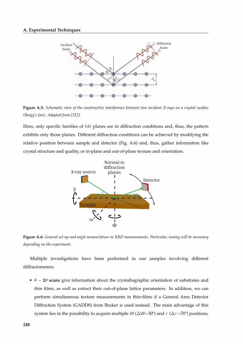
A. Experimental Techniques
αθ
θ
1
2
1’
2’Incident
beamDiffracted
beam
dhkl
Figure A.5: Schematic view of the constructive interference between two incident X-rays on a crystal surface
(Bragg's law). Adapted from [322].
films, only specific families of hkl planes are in diffraction conditions and, thus, the pattern
exhibits only those planes. Different diffraction conditions can be achieved by modifying the
relative position between sample and detector (Fig. A.6) and, thus, gather information like
crystal structure and quality, or in-plane and out-of-plane texture and orientation.
X-ray source
Sample
Detector
Normal todiffraction
planes
χ
ω
ω
Φ
2θ
Figure A.6: General set-up and angle nomenclature in XRD measurements. Particular, tuning will be necessary
depending on the experiment.
Multiple investigations have been performed in our samples involving different
diffractometers:
• 2 scans give information about the crystallographic orientation of substrates and
thin films, as well as extract their out-of-plane lattice parameters. In addition, we can
perform simultaneous texture measurements in thin-films if a General Area Detector
Diffraction System (GADDS) from Bruker is used instead. The main advantage of this
system lies in the possibility to acquire multiple 2 (2=30º) and τ (τ=70º) positions,
248

A.3. Structural characterization
and reduce the acquisition time extraordinarily, as well as give information about the
out-of-plane texture. Thus, 2D-XRD is highly recommended for samples with different
phases, i. e. with single-crystalline and random orientations. Fig. A.7 compares the
results obtained using 1D (Fig. A.7a) and 2D (Fig. A.7b) detectors of the same sample.
Further information on the working principles of XRD2 can be found elsewhere [323].
This measurements were performed with a Rigaku Rotaflex RU-200BV diffractometer at
2θ
CG
O(0
22)
YSZ(0
02)
CG
O(1
11)
CG
O(0
02)
χ
(a) (b)
CG
O(0
22)
YSZ(002)C
GO
(002)
CG
O(1
11)
k
20 25 30 35 40 45 50102
103
104
105
106
Inte
nsity
(a.u
.)
θ−2θ
Figure A.7: 2 measurements with (a) 1D and (b) 2D detectors of a CGO multilayered sample on a YSZ
substrate.
ICMAB and a PANalytical XPert Pro MPD theta-theta Diffractometer at MRI, both with
a Cu-K source (λCu =1.5418 A). Data acquisition was typically performed with a 0.02º
step size.
In addition, microstructural analysis can be performed from characterization of line
broadening at specific diffraction peaks. High-resolution XRD (HRXRD) measurements
are often used since this widening is highly affected by instrumental aberrations and in
some cases there is an overlap between film and substrate reflections. Nevertheless, the
diffracted intensity is significantly reduced and, therefore, acquisition times are quite
long. A detailed description of these analyses will be given in section A.3.2.
Measurements of specific 2 positions were done in a PANalytical XPert PRO MRD
4-circle diffractometer in high resolution mode (λCu1 =1.5406 A) from the Catalan Institute
of Nanoscience and Nanotechnology (ICN2). Also, a standard powder diffractometer
located at ICMAB (Siemens D5000, λCu1 =1.5406 A and λCu2 =1.5444 A) was used prior
measurement of a LaB6 standard sample in order to determine the instrumental
broadening.
249

A. Experimental Techniques
• Rocking curves or !-scans provide information about the out-of-plane texture of a
sample in a different way than the information obtained from XRD2. By performing an
! scan at a fixed 2 position of a low indexed peak and analyzing the full width at half
maximum (FWHM) ! of the curve acquired, we can obtain information on the
mosaicity of the analyzed reflection. The narrower the peak, the higher the crystalline
quality of the sample. Some examples can be found in section 2.1.2.
This measurements were performed with a Rigaku Rotaflex RU-200BV diffractometer at
ICMAB. Data acquisition was typically performed with a 0.02º step size.
• Pole figures or π-scans allow us to represent the distribution of crystallographic lattice
orientations between films and substrates. Basically, it consists of measuring a specific
hkl reflection set in Bragg condition. If the (hkl) planes are not parallel with the substrate,
the sample must be tilted an angle τ and, then, a π-scan of frequently 360º is perform
at that angle. Pole figures are understood as the stereographic projection of the selected
hkl-planes situated in an imaginary hemisphere located above the sample surface (Fig.
A.8a). In Figs. A.8b and c, we can see the integration of a specific 2 position and the
resulting pole figure, respectively.
This measurements were performed with a GADDS diffractometer at ICMAB. Pole
figures were typically done at fixed 2τ regions and π-scans with 180 steps of 2º for 40
seconds each one.
(a) (b) (c)
Φ
Φ
Φ
Figure A.8: (a) Schematic representation of the stereographic projection of a certain hkl-plane on a 2D image
consisting of a circle with 0º π 360º and 0º τ 90º. (b) XRD2 frame centered at 2 =28.5º and τ =54º
belonging to a CeO2 nanostructured sample. The pole figure is built from the integration between 27º< 2 <29º
(marked in blue) of 180 equivalent frames at different π-angles. (c) Resulting pole figure of the (111)CeO2
reflection. The peaks situated at τ =54º correspond to (001)-oriented CeO2 nanoislands.
250

A.3. Structural characterization
• Epitaxial and random fraction quantification is possible if one follows a variation of the
procedure employed by A. Llordés in our group [5, 245]. This method makes use of a 2D
detector to set the sample on a certain asymmetric reflection, i. e. fixed values of 2, !
and τ. Then, a π-scan is performed to find the maximum value of that angle, and once it
is found the acquisition begins. Following this methodology coupled with the addition
of a nickel filter, we are able to eliminate the contribution of substrate’s Kbeta and possible
influence of substrates in most cases. The reflections chosen to perform our analyses are
the (011) and (022) orientations which corresponds to values of !〈15º, τ=45º and 2 will
depend on the oxide analyzed (2CZO=47.73º, 2LNO=32.78º and 2BST=31.67º). The
acquisition time was of 30 min to 1 h and the measurements were done using the GADDS
system at ICMAB.
Fig. A.9 shows an example of the result after the measurement for a 3-layered BST film
grown on LAO with RTA at 900 ºC, 20 ºCs1 for 30 min in O2. Data analysis is done
by integrating the areas selected in Fig. A.9 with GADDS software and using any data
analysis/graphing suite. Essentially, the background (Ibkg) is substracted from the other
contributions, and the random part is removed from the epitaxial one as well. Then, area
integration of the remaining curves is performed using the same analysis software. The
relation between epitaxial and random fractions can be extracted from
IrandomIepitaxial
=Iexpring (360=τ) 4β
8 Iexppole
; (A.1)
where Iexpring and Iexppole are the random and epitaxial contributions as indicated in Fig. A.9,
and τ is fixed for each analysis. Finally, it contribution can be calculated if we assume
(011)STO (011)BST
Ipole
Iring Ibkg
Figure A.9: Example of the quantification of the epitaxial and random fractions for a 3-layered BST film grown
on LAO. The growth was done with RTA at 900 ºC, 20 ºCs1 for 30 min in O2.
251

A. Experimental Techniques
that Irandom and Iepitaxial are representative of the volumic fraction of each phase (vrandom
and vepitaxial), and that Irandom + Iepitaxial = 100.
• X-ray reflectometry (XRR) uses low angles, i. e. grazing incidence, to characterize
thickness of thin films and multilayers, surface roughness and density, etc. Basically, the
X-ray beam is reflected above a critical angle c〈0.3º at film surfaces and interfaces due
to different electron densities generating an interference oscillatory pattern (Fig. A.10).
XRR has been used in this thesis to analyze the thickness of different oxide thin-films by
using the relation
〈 λ
t; (A.2)
where is the periodicity between oscillations, λ is the characteristic wavelength of the
X-ray source, and t is the thickness of the film. Thicknesses extracted from Fig. A.10 are
approximately 45 nm and 30 nm for pyrolyzed and grown LSMO films, respectively.
Grazing angle (º)
Inte
nsity
(a.
u.)
0.5 1.0 1.5 2.0 2.5 3.01
10102
103
104
105∆θ
θc~0.5º
LSMOpyrolyzed
LSMO grown
Figure A.10: X-ray reflectometry (XRR) measurement of pyrolyzed (—) and grown (—) La0.7Sr0.3MnO3 thin-
films on SrTiO3 substrates. c indicates the critical angle and the periodicity between oscillations.
This measurements were performed with a Rigaku Rotaflex RU-200BV at ICMAB (from
0.5º to 3º with steps of 0.002º and λCu=1:5418 A) and a PANalytical XPert PRO MRD
4-circle located at the ICN2 (from 0.5º to 6.5º with steps of 0.02º and λCu1 =1:5406 A).
• Reciprocal space maps (RSMs) or Q-plots give us information about the structural
properties of thin films such as in-plane and out-of-plane lattice parameters and
relaxation, and structural quality. The measurements consists of a series of !2 scans
performed at fixed π and τ values around specific reflections of substrate and film,
usually asymmetric, and allowing us to record a complete area of the reciprocal space.
Information about lattice relaxation can be acquired if we transform the !
252

A.3. Structural characterization
information to the reciprocal space wavevectors parallel and perpendicular to the
surface, Qx and Qz respectively, using the following relations:
Qx =λ
2sin sin( !) (A.3a)
Qz =λ
2sin cos( !) (A.3b)
where λ is the wavelength of the X-ray source and Qx and Qz are the reciprocal space
wavevectors. Values of the in-plane and out-of-plane lattice parameters, a and c
respectively, are extracted from the corrected center positions of peaks, considering the
experimental displacement in and !. Then, the lattices parameters can be extracted
from:
a =h
Qx(A.4a)
c =l
Qz(A.4b)
where h and l stand for the Miller indices of the peak. This measurements were
performed with a PANalytical XPert PRO MRD 4-circle diffractometer located at ICN2.
Fig A.11 shows an example of a RSM of the (-224) asymmetric orientation for CZO on
YSZ.
0.800.79
0.780.77
0.76
0.75
0.740.73
-0.57 -0.56 -0.55 -0.54 -0.53 -0.52Qx (r.l.u.)
Qz (
r.l.u
.)
Figure A.11: Example of a reciprocal space map of the (-224) asymmetric orientation for CZO on YSZ.
Additional knowledge about XRD physical principles and applications can be found
elsewhere [324].
253

A. Experimental Techniques
A.3.2 Microstructural analysis from XRD measurements
Generally, oxide thin-films possess crystalline structures which differs from the ideal case.
This variations are known as microstructure and can have a deep control over their properties
[202, 203]. The most important parameter controlling the microstructure is the residual stress
which can be caused by processing, lattice mismatch between film and substrate, differences
in thermal expansion coefficients, and crystallographic defects such as dislocations, stacking
faults, grain boundaries, etc. X-ray diffraction is a good tool that can be used to measure
lattice disorders by analyzing the shift and broadening of peaks.
Residual stresses are originated by strain and can be classified in
• macrostrain (ξ): its a large-range effect caused by a uniform strain and produces a shift
of the diffraction lines. For example, a compressed film will have a smaller interplanar
distance dhkl and present a shift towards higher values of 2, while if the strain is tensile
dhkl will be larger and the displacement will be to lower angles. Usually, this strain is
seen at early stages of growth before dislocations are introduced in the film structure or in
systems with relatively low lattice mismatch which prefer to be slightly strained. Besides
typical 2 measurements, reciprocal space maps are also a good tool to analyze this
source of strain.
• microstrain (µ): its a short-range fluctuation in the interplanar distance generated by
a non-uniform strain and produces a broadening of the diffraction peak. Its origin is
due to the misorientation of grains and the presence of grain boundaries. Main sources
of microstrain are crystal defects like dislocations, grain and twin boundaries, stacking
faults, vacancies, but also mechanical deformation or compositional gradients.
Besides lattice distortions, peak broadening is also influenced by domain size (grain or
particle size) which is independent of the order of the (hkl) reflection. The Williamson-Hall
plot [325] is the simplest model to separate between both contributions, and has been
previously used in our group to calculate the microstrain of YBCO nanocomposites
[5, 115, 245]. Basically, it uses the different dependence on the Bragg angle of size s and
microstrain m broadening
s =Kλ
L cos ; (A.5)
and
m = 4ν tan : (A.6)
254

A.3. Structural characterization
Eq. A.5 is the well-known Scherrer formula [326], where K is a constant with a typical value
of 0.9, λ is the wavelength of the X-ray source, and L is the average domain size. Eq. A.6 was
derived by Stokes and Wilson [327], where ν is the microstrain.
Assuming a Gaussian profile, the real microstrain broadening is 2hkl=
exphkl
2instrhkl
2,
and the W-H equation results in
2hkl cos2 =
∫Kλ
L
]2
+ 16ν2 sin2 : (A.7)
In this thesis, we have used the Williamson-Hall plot to evaluate isotropic variations of
the disorder parameter along out-of-plane orientations, in our case (00l) reflections, from the
graphical representation of 2hkl cos2 versus sin2 for different 00l diffraction peaks as shown
in Fig. A.12 for a Ba0:8Sr0:2TiO3 thin-film grown on a LaAlO3 substrate.
0.0
0.2
0.4
0.6
0.8
1.0
0.0 0.2 0.4 0.6sin2θ
(002)
10-4β2
cos2 θ (004)(003)
(001)
KLλ 2
Slope=16 2µ
Figure A.12: Microstructural analysis of a Ba0.8Sr0.2TiO3 thin-film grown on a LaAlO3 substrate using the
Williamson-Hall plot method.
Basically, the ! angle was centered on the film, the ! range was reduced to minimize
substrate’s contribution and the acquisition time was increased to 30-60 min.
A.3.3 Transmission Electron Microscopy (TEM)
Transmission Electron Microscopy (TEM) is an extremely robust tools to analyze the internal
structure of materials with sub-nanometer resolution (〈0.5 A) in the case of
aberration-corrected microscopes [328]. In essence, TEM consists in a parallel static beam of
coherently accelerated electrons (〈100-300 kV) which interacts with a sample. There electrons
scatter with the atoms of the specimen and generate diffraction patterns. Electrons travelling
across the sample are magnified and focused by a series of electromagnetic lenses to finally
255

A. Experimental Techniques
gather all information containing its atomic distribution in an image. The fundamental
elements of a conventional TEM microscope are depicted in Fig. A.13a.
The same working principles are applied in Scanning Transmission Electron Microscopy
(STEM), yet with a small difference in the electron beam incidence on the sample where a
convergent beam is scanned through it. This is achieved by placing the objective lens before
the specimen (Fig. A.13b).
Specimen
Objectivelens
Back focalplane
Imageplane
(a) (b)
High anglescattered electrons
ADFdetector
BF detector
Figure A.13: (a) Simple representation of the main components present in a Transmission Electron Microscope.
(b) Illustrative view of a STEM microscope. Figure has been adapted from [329].
Besides imaging and modifying the position of the electromagnetic lenses, TEM can
perform Electron Diffraction (ED) and spectroscopies like Electron Energy Loss spectroscopy
(EELS) which give information about the chemical and structural composition of an specimen.
The information obtained from ED and imaging is generated by coherently and elastically
scattered electrons3.
On the other hand, electrons scattered inelastically at high angles, typically incoherent, are
used for High Annular Dark Field (HAADF) STEM imaging. It is worth noting, and has
already been demonstrated, that their intensity is proportional to Z2 (Z is the atomic number)
[330]. This means that the heavier the atom, the brighter will be its contrast, leading to an
unambiguous interpretation of its chemical nature. Furthermore, while operating a STEM, the
non-scattered beam can be selected as well and, thus, STEM imaging is quite similar to TEM
Bright Field imaging.
Although High Resolution TEM (HRTEM) provides atomic resolution, STEM is in a
3Coherently scattered electrons are those that preserve their energy and a certain phase relationship between
them after their interaction with the sample.
256

A.3. Structural characterization
preferential position since image interpretation is more straightforward. This is because
HRTEM contrast is due to phase differences of the scattered beams which means that the
images will highly depend on sample thickness and microscope defocus. Also, interpretation
of HRTEM results often necessary to perform simulations to univocally determine the origin
of the contrasts observed.
Most limitations in TEM and STEM are caused by lens aberrations like astigmatism,
chromatic and spherical aberrations, and by the quality of the sample, particularly its
thickness. For a specimens to be transparent to electrons, its thickness must be of few tens of
nanometers (< 100 nm).
Practically all samples were prepared by mechanical polishing at ICMAB with the exception
of samples containing stainless-steel that were prepared by FIB. After the mechanical polishing
process, the specimen has a thickness 〈20 νm, so to reduce its thickness to the required values
an Ar+ ion bombardment using a Precision Ion Polishing System (PIPS) is performed. This
process was exclusively carried out by M. de la Mata and F. Belarre. Further details about
sample preparation or the techniques are exhaustively described in dissertations from other
members of our group specialized in these techniques [329, 331] and in the book from Williams
and Carter [328].
Different microscopes were used for the HRTEM and STEM characterization of our
samples. For instance, HRTEM images were acquired in a Jeol 2010 FEG (200 kV) at “Serveis
Científico-Tècnics” of UB and a FEI F20 (200 keV) at ICN2. HAADF images were obtained in a
probe corrected FEI Titan 60-300 operated at 300 kV and located at the Advanced
Microscopies Laboratory (LMA) from the Institute of Nanoscience of Aragon (INA). Image
acquisition and interpretation was carried out by M. de la Mata using the DigitalMicrograph
software (Gatan Inc.) and 3D atomic models with the Rhodius Software [332].
A.3.4 Reflection High-Energy Electron Diffraction (RHEED)
Reflection High-Energy Electron Diffraction (RHEED) is a diffraction technique extremely
sensitive to morphology and structure of surfaces with a sensitivity as thin as a monolayer
[333]. This makes RHEED a very appropiate tool either to characterize the morphology of flat
surfaces or to control the growth of thin films, and provides complementary information to
XRD and TEM.
The setup employed in RHEED measurements is composed of an electron gun which
produces a beam of electrons, is located in a vacuum chamber to prevent them from scattering
257

A. Experimental Techniques
by gas molecules, typically operates at 10-100 keV, and probably is the most significant part
because it limits the resolution of the system.
The electrons flowing from the source hit a sample at extremely small angles in relation to
its surface which ensures a high surface sensitivity and reduces the contribution from the
substrate. A small fraction of incident electrons generate a diffraction pattern when they
interfere constructively at certain angles. Electrons interfere according to the position of atoms
on the sample surface, so the diffraction pattern at the detector is a function of the sample’s
surface. If it is perfectly flat, the pattern presents a group of concentric spots known as Laue
circles. Fig. A.14 presents a simplistic representation of the elastic scattering of electrons and
the formation of the reciprocal diffraction pattern.
Figure A.14: Three-dimensional schematic representation of electron scattering in the real space and its
corresponding pattern in the reciprocal space. Reproduced from [334].
However, most surfaces are imperfect and, thus, the shape of the diffraction pattern is
modified by splitting or broadening of its peaks. The pattern for rough surfaces is
characterized by spots consists in straight lines since high energy electrons penetrate through
surface irregularities (Fig. A.15a). When crystals size is reduced, the diffraction spots enlarge
in the direction of decrease as exemplified in Figs. A.15b and c. Finally, surfaces with flat
terraces present patterns which incorporates reflected and transmitted electron (Fig. A.15d).
An amorphous surface shows a blurred background instead of a diffraction pattern.
Measurements of the crystallographic structure of ultrathin-films and interfacial
nanoislands were obtained at ICMAB using a RHEED system (Staib Instrumente GmbH) with
an electron gun of 30 kV, a current of about 50 νA and an incidence angle of less than 4º with
respect to the substrate surface.
258

A.4. Physical properties measurements
(a) (b)(b)
(c) (d)
Figure A.15: Sketch of the various surface morphologies and RHEED diffraction patterns associated to them.
A.4 Physical properties measurements
A.4.1 Rheological and contact angle measurements
Viscosity and contact angle with the substrate are critical parameters which determine the
proper wettability of precursor solutions over substrates. The former controls, along with
molarity and deposition conditions, the final thickness of the films. Theoretically, viscosity (η)
measures the resistance of a fluid to deformation by shear or tensile stress. The measurement
of viscosity in our precursor solutions involves the deposition of a small volume of solution
between to plates of a rheometer (Haake RheoStress 600 from Thermo Fisher Scientific Inc.),
which are covered with a glass hood to avoid evaporation of solvent. Then, the instrument
applies a torque force to maintain a preset rotational speed of the upper plate. This force is
registered continously and allows the calculation of the shear stress (τ) and viscosity using a
specific software. Fig. A.16a shows an example of the data acquired; viscosity values are
extracted from the stable range of the measurement.
The later quantifies the wettability of the precursor solution over a substrate. A small drop
of solution is deposited on a substrate, its trajectory is recorded and the contact angle is
extracted precisely at the moment when the drop makes contact with the surface. Fig. A.16b
presents an image of the drop used to measure the contact angle. The equipment employed
was a Drop Shape Analyzer DSA100 from Krüss Gmbh.
259

A. Experimental Techniques
0 2000 4000 6000 8000 10000
0.00215
0.00220
0.00225
0.00230
0.00235
0.00240
0.00245
η (P
a·s)
t (s)
(a)
(b)
Figure A.16: Typical data obtained from (a) viscosity, and (b) contact angle measurements.
A.4.2 UV-Vis-NIR spectroscopy
UV-Vis-NIR spectroscopy is an absorption technique that uses light from the near-IR to near-
UV. In this region of the electromagnetic spectra, molecules undergo electronic transitions and
lead to characteristic absorption of light as a function of the wavelength (λ). This spectroscopic
technique is mainly used to characterize quantitatively solutions containing transition metals
or highly conjugated organic compounds. However, we have used this technique for the optical
characterization of CSD-deposited thin-films.
It is based on the Lambert-Beer law which establishes an exponential relationship between
the intensity of incident light at a given wavelength that goes into a medium and the intensity
of light transmitted.
It = I0 exp (l) (A.8)
where It is the trasmitted intensity, I0 is the intensity of the incident light at a given wavelength,
is the absorption coefficient and l the pathlength through the sample.
The spectrophotometer mesures the intensity of light that goes through a sample and
compares it with the initial intensity. The relation I=I0 is called transmitance and can be
expressed in percentages. An spectrophotometer consists of a light source composed by a
tungsten (300-2500 nm) and a deuterium lamp (190-400 nm), a sample holder (the same used
in the FTIR spectroscopy in section A.1.1), a diffraction slit or a monochromator to split the
260

A.4. Physical properties measurements
different wavelengths and a detector which is tipically a photodiode or a CCD camera.
The measurements from this work have been obtained with UV-Vis-NIR Cary 5000
spectrophotometer (Varian). Highly transparent quartz or alumina substrates have been used
to measure the optical properties of both the as-deposited metal-organic and the pyrolyzed
films. The range of measure has been chosen to be from 200 to 1100 nm, since the wavelength
of the Nd:YAG laser used are within this range.
However, our samples are partially transparent and, thus, reflectance measurements are
also required for the complete characterization of our samples. For this purpose, we attached
a device called integrating sphere to the spectrophotometer which consists of a spherical cavity
made of a reflective coating, and collects the light specularly and diffusively reflected on the
sample. Then, using transmitance and reflectance measurements and knowing the thickness
of our films, we can applied a model designed by Denton et al. [284] to calculate the complex
refraction indexes (n and k) from which the absorption coefficient () can be extracted using the
following formula:
=4βk
λ(A.9)
A.4.3 Ellipsometry
The word "ellipsometry" has its origin in the fact that elliptically polarized light is employed
during the measurement. Basically, it consists of the investigation of the dielectric properties
of thin films such as the complex refractive index or the dielectric function by measuring the
change in light polarization when interacts with a material, i. e. reflection at non-normal
incidence. Fig. A.17 illustrates a schematic representation of the ellipsometry setup.
The change in polarization α, commonly written as α = tan exp (i) is quantified by
(a) (b)
Figure A.17: Schematic representation of (a) the ellipsometry setup, and (b) the light path for multi-layered
samples.
261

A. Experimental Techniques
two magnitudes, the amplitude ratio and the phase difference as defined in [335]. Then,
thickness, composition, porosity, surface roughness and optical constants can be extracted by
fitting those functions with a model. The need to model the data is the main difficulty of this
technique which sometimes can be extremely complicated.
For semi-transparent films, the most simple model is the Cauchy dispersion law:
n = A+B
λ2+C
λ4; k =
D
λ+E
λ3+F
λ5(A.10)
where A, B, C, D, E and F are constants, and λ is the wavelength. However, if the system
is rather complex, a modified Cauchy law or a Tauc-Lorentz model may be more valid4. Fig.
A.18 shows the typical data obtained from ellipsometry measurements
Ellipsometry measurements were performed at ICMAB with a GES5E ellipsometer.
1.5 2.0 2.5 3.0 3.5 4.0 4.5 5.0
-0.8
-0.4
0.0
0.4
0.8
tan(Ψ)
cos(∆)
E ( eV )
(a) (b)
0.00.51.01.52.02.53.03.5
1.5 2.0 2.5 3.0 3.5 4.0 4.5 5.0E ( eV )
n
k
Figure A.18: (a) Data obtained from ellipsometry measurements of CZO films on YSZ, tan (solid lines) and
cos (dashed lines) for experimental values (black lines) and fitted values (red lines) at an angle of 70º. (b)
Refractive index n (- - -) and extinction coefficient (- - -) obtained applying the Tauc-Lorenz model. n and k data
from Ref. [336] are plotted for comparison.
A.4.4 Electric transport measurements
Electric transport measurements on LNO films have been performed using a Physical
Properties Measurements System (PPMS) from Quantum Design located at the ICMAB. The
system has a 9 T superconducting magnet and a helium cryostat which allows a precise
temperature control between 1.8 K and 400 K. In addition, it incorporates a nano-voltmeter
and a AC/DC current source which provides currents down to 1 νA and up to 2 A with a
4A summary of the multiple dispersion laws available can be found in the user’s manual of the SOPRA GES5E
ellipsometer.
262

A.4. Physical properties measurements
resolution of 0.1 µ A. Vacuum grease is used when mounting the sample in order to ensure a
good thermal coupling. Furthermore, a thermometer is found just below the sample
mounting space to monitor the sample temperature.
In order to determine the resistivity of thin films, we have mounted our samples with a four-
point configuration which allow us to avoid the contribution of contact resistivity (silver). Fig.
A.19 presents an sketch of the measurements, where current is applied through two contacts
(M and N) and voltage is measured on the other two (O and P). Then, a second measurement is
performed by applying current through two other contacts (P and M) and voltage is measured
on the remaining ones (O and N).
I+
I-
V+
V-
MN
OP
MN
OP
I+
I-
V+
V-
Figure A.19: Van der Pauw configuration employed to perform resistivity measurements.
We calculate the resistivity following the van der Pauw method [337], in essence, after the
measurements we define ρ as
ρ =πt
ln 2
RMN,OP +RNO,PM2
f (A.11)
where RMN,OP=(VP −VO)/IMN and RNO,PM=(VM −VP )/INO are the resistances for the two
measurements, t is the thickness of the sample, and f is a multiplying factor between 0 and 1
and depends on the ratio RMN,OP
RNO,PM.
A.4.5 Superconducting quantum interference device (SQUID)
A superconducting quantum interference device (SQUID) is a very sensitive magnetometer
utilized for the measurement of incredibly small magnetic fields. This can be achieve thanks
to a superconducting loop with one or two weak links (Josephson junctions) inserted in these
devices. In essence, they generate an output voltage signal, which is a periodic function of the
magnetic flux threading the loop, a geometry known as DC-SQUID (constant bias current).
263

A. Experimental Techniques
The magnetometer consists of a SQUID system and a precision temperature control unit
attached to a high-field superconducting coil. The sample is put inside the coil producing a
uniform dc-magnetic field at its location. Once the sample is magnetized, it is moved through
a set of pickup coils inducing a current in the detection system which is proportional to the
variation of magnetic flux. This signal is amplified via a sensor in form of voltage. Therefore,
the magnetic moment of the sample is proportional to voltage variations detected with the
SQUID, which can resolve magnetic moments as subtle as 106 emu. The whole system goes
inside an helium cryostat whose function is to refrigerate the superconducting coil and
provides precise temperature control.
Field and temperature dependent magnetization curves of LSMO thin films were
measured at ICMAB using a commercial MPMS XL-7T SQUID DC-magnetometer (Quantum
Design) equipped with a 7 T superconducting coil and a helium cryostat with temperature
control from 1.8 to 400 K. The isothermal magnetization curves presented a strong negative
slope due to the diamagnetic contribution of the single crystal substrates. Data treatment
involved the withdrawal the aforementioned contribution by linear fitting of the diamagnetic
signal.
A.4.6 Piezoresponse Force Microscopy (PFM)
The investigation of ferroelectric properties can be done through measurement of
piezoelectricity since both phenomena are connected, i. e. ferroelectric materials are also
piezoelectric [338].
Piezoresponse Force Microscopy (PFM) is a local technique based on the working
principles of AFM characterization (section A.2.1) operating in the so-called contact-mode.
The application of an electrical stimulus in the form of a periodic (or AC) voltage to a
conductive tip leads to a local deformation of the sample causing the tip/cantilever to deflect
(Fig. A.20). Since a laser/photodiode system is used to adjust the position of the tip (section
A.2.1), any change of the laser position on the photodiode is recorded by a lock-in amplifier.
The measured signal is proportional to the material’s piezoresponse. Typically, PFM measures
the ferroelectric domains of a selected region where the amplitude of the cantilever deflection
is proportional to the piezoelectric coefficient and the phase indicates the orientation of the
ferroelectric domain.
Besides measuring the ferroelectric domains by applying an alternating voltage Vac (1-10
V) to the tip, PFM can also be used to change the polarization of small regions of a sample by
264

A.4. Physical properties measurements
Figure A.20: Piezoresponse Force Microscopy operation and deformation cause on samples' surface during the
application of an alternating voltage. Image courtesy of S. Jesse from ORNL.
using a continuous voltage Vdc or bias, i. e. lithography. Then, reading of the written domains
is done using an AC voltage as we mentioned previously. The Vdc must be sufficiently high
(larger than the coercive field) to be able to polarize the desired area without modifying the
material’s surface. The Vac reading voltage must be lower than the coercive field to prevent
domain rewriting. For instance, Fig. A.21a depicts a BST film with two ferroelectric domains
with inverse polarization after applying a bias of -7 V (inner region) and +7 V (outter region).
The reading voltage employed in this case was 2.5 V.
PFM spectroscopic measurements can also be carried out, obtaining hysteresis loops of the
ferroelectric behavior. Essentially, a reading voltage is applied to the tip and the bias voltage is
varied. The change in amplitude and phase signals are then recorded leading to the common
hysteresis loops. Figs. A.21b and c illustrate the variation of amplitude and phase as the Vdc
applied to the sample changes. Finally, calculation of the piezoelectric coefficient, i. e. the d33
component, can be obtained from
d33 =A
VacQ; (A.12)
(b)
-8 -6 -4 -2 0 2 4 6 80.0
0.1
0.2
0.3
Am
plitu
de (
nm)
Sample Bias (V)-8 -6 -4 -2 0 2 4 6 8
Sample Bias (V)
0306090
120150
180
Phas
e (º
)
(c)(a)
+7 V
-7 V
Figure A.21: Piezoresponse Force Microscopy (PFM) measurements of a BST film annealed at 900 ºC, 20 ºCs1
for 30 min in O2. (a) PFM phase image showing the written domains with a voltage of +7 V (outter square) and
-7 V (inner square). Hysteresis loops are representative of (b) amplitude and (c) phase.
265

A. Experimental Techniques
where A is the amplitude, Vac is the reading alternating voltage and Q is the so-called quality
factor of the cantilever. Usually, the d33 is calculated at the maximum amplitude Amax (at the
resonance frequency Ψres) and the quality factor is defined as
Q =Ψres
Ψhigh Ψlow; (A.13)
where Ψlow and Ψhigh are the frequency values below and above Ψres that fulfil the condition
A=Amax=p
2. Notice that a gain is usually applied during the measurement, therefore, it must
be subtracted when calculating the piezoelectric coefficient. Fig. A.22 illustrates the
amplitude/frequency curve from where Ψres and Q can be determined. A more detailed
description of PFM working principles, imaging, spectroscopies and additional measurements
can be found elsewhere [231, 339, 340].
110 115 120 125 130 135 1401
2
3
4
5
Am
plitu
de (
nm)
Frequency(kHz)
νlow νhigh
νres
Figure A.22: Example of a frequency curve used to determine the resonance frequency and the Q factor.
PFM measurements where done at ICMAB with an Agilent 5500LS from Agilent
Technologies. Triangular silicon tips coated with 100 nm of doped diamond from APPNANO
were mounted on Si cantilevers with force constants around 0.1-0.6 Nm1 and resonance
frequencies from 11 to 18 kHz. Data analysis was carried out using MountainsMap 7.0
software from Digital Surf.
266

Bibliography
[1] E.P. MURRAY, T. TSAI, and S.A. BARNETT. «A direct-methane fuel cell with a ceria-based anode.» Nature,
400(6745), 649, 1999.
[2] R. RAMESH. «Ferroelectrics: A new spin on spintronics.» Nature Materials, 9(5), 380, 2010.
[3] I. VREJOIU, M. ALEXE, D. HESSE, and U. GOSELE. «Functional Perovskites - From Epitaxial Films to
Nanostructured Arrays.» Advanced Functional Materials, 18(24), 3892, 2008.
[4] W. EERENSTEIN, N.D. MATHUR, and J.F. SCOTT. «Multiferroic and magnetoelectric materials.» Nature,
442(7104), 759, 2006.
[5] A. LLORDES, A. PALAU, J. GAZQUEZ, M. COLL, R. VLAD, A. POMAR, J. ARBIOL, R. GUZMAN, S. YE, V.
ROUCO, F. SANDIUMENGE, S. RICART, T. PUIG, M. VARELA, D. CHATEIGNER, J. VANACKEN, J. GUTIERREZ,
V. MOSHCHALKOV, G. DEUTSCHER, C. MAGEN, and X. OBRADORS. «Nanoscale strain-induced pair
suppression as a vortex-pinning mechanism in high-temperature superconductors.» Nature Materials, 11(4),
329, 2012.
[6] X. MARTÍ, I. FINA, C. FRONTERA, J. LIU, P. WADLEY, Q. HE, R.J. PAULL, J.D. CLARKSON, J. KUDRNOVSKÝ,
I. TUREK, J. KUNEŠ, D. YI, J.H. CHU, C.T. NELSON, L. YOU, E. ARENHOLZ, S. SALAHUDDIN, J.
FONTCUBERTA, T. JUNGWIRTH, and R. RAMESH. «Room-temperature antiferromagnetic memory resistor.»
Nature Materials, 13(4), 367, 2014.
[7] T. ITO and S. OKAZAKI. «Pushing the limits of lithography.» Nature, 406(6799), 1027, 2000.
[8] J.V. BARTH, G. COSTANTINI, and K. KERN. «Engineering atomic and molecular nanostructures at surfaces.»
Nature, 437(7059), 671, 2005.
[9] F.F. LANGE. «Chemical Solution Routes to Single-Crystal Thin Films.» Science, 273(5277), 903, 1996.
[10] R.W. SCHWARTZ, T. SCHNELLER, and R. WASER. «Chemical solution deposition of electronic oxide films.»
Comptes Rendus Chimie, 7(5), 433, 2004.
[11] X. OBRADORS, T. PUIG, M. GIBERT, A. QUERALTÓ, J. ZABALETA, and N. MESTRES. «Chemical solution route
to self-assembled epitaxial oxide nanostructures.» Chemical Society Reviews, 43(7), 2200, 2014.
[12] D. HRADIL, T. GRYGAR, J. HRADILOVÁ, and P. BEZDI CKA. «Clay and iron oxide pigments in the history of
painting.» Applied Clay Science, 22(5), 223, 2003.
267

BIBLIOGRAPHY
[13] M. DAWBER, K.M. RABE, and J.F. SCOTT. «Physics of thin-film ferroelectric oxides.» Reviews of Modern
Physics, 77(4), 1083, 2005.
[14] Y. TOKURA. «Critical features of colossal magnetoresistive manganites.» Reports on Progress in Physics, 69(3),
797, 2006.
[15] K.A. BOGLE, J. CHEUNG, Y.L. CHEN, S.C. LIAO, C.H. LAI, Y.H. CHU, J.M. GREGG, S.B. OGALE, and
N. VALANOOR. «Epitaxial Magnetic Oxide Nanocrystals Via Phase Decomposition of Bismuth Perovskite
Precursors.» Advanced Functional Materials, 22(24), 5224, 2012.
[16] W.C. CHUEH, C. FALTER, M. ABBOTT, D. SCIPIO, P. FURLER, S.M. HAILE, and A. STEINFELD. «High-Flux
Solar-Driven Thermochemical Dissociation of CO2 and H2O Using Nonstoichiometric Ceria.» Science, 330,
1797, 2010.
[17] C.A. COPETTI, H. SOLTNER, J. SCHUBERT, W. ZANDER, O. HOLLRICHER, C. BUCHAL, H. SCHULZ, N.
TELLMANN, and N. KLEIN. «High quality epitaxy of YBa2Cu3O7−x on silicon-on-sapphire with the multiple
buffer layer YSZ/CeO2.» Applied Physics Letters, 63(10), 1429, 1993.
[18] L. TYE, N.A. EL-MASRY, T. CHIKYOW, P. MCLARTY, and S.M. BEDAIR. «Electrical characteristics of epitaxial
CeO2 on Si(111).» Applied Physics Letters, 65(24), 3081, 1994.
[19] M.A. SAINZ, A. DURÁN, and J.M. FERNÁNDEZ NAVARRO. «UV highly absorbent coatings with CeO2 and
TiO2.» Journal of Non-Crystalline Solids, 121(1-3), 315, 1990.
[20] N. ÖZER. «Optical properties and electrochromic characterization of sol–gel deposited ceria films.» Solar
Energy Materials and Solar Cells, 68(3-4), 391, 2001.
[21] X. OBRADORS, T. PUIG, A. POMAR, F. SANDIUMENGE, N. MESTRES, M. COLL, A. CAVALLARO, N. ROMA,
J. GAZQUEZ, J.C. GONZALEZ, O. CASTANO, J. GUTIERREZ, A. PALAU, K. ZALAMOVA, S. MORLENS, A.
HASSINI, M. GIBERT, S. RICART, J.M. MORETO, S. PINOL, D. ISFORT, and J. BOCK. «Progress towards all-
chemical superconducting YBa2Cu3O7-coated conductors.» Superconductor Science & Technology, 19(3), S13,
2006.
[22] M.S. CHEN, T.B. WU, and J.M. WU. «Effect of textured LaNiO3 electrode on the fatigue improvement of
Pb(Zr0.53Ti0.47)O3 thin films.» Applied Physics Letters, 68(10), 1430, 1996.
[23] S. RAKSHIT and P.S. GOPALAKRISHNAN. «Oxygen Nonstoichiometry and Its Effect on the Structure of
LaNiO3.» Journal of Solid State Chemistry, 110(1), 28, 1994.
[24] D. BAO, X. YAO, N. WAKIYA, K. SHINOZAKI, and N. MIZUTANI. «Preparation of conductive LaNiO3 film
electrodes by a simple chemical solution deposition technique for integrated ferroelectric thin film devices.»
Journal of Physics D: Applied Physics, 36(10), 1217, 2003.
[25] H. MIYAZAKI, T. GOTO, Y. MIWA, T. OHNO, H. SUZUKI, T. OTA, and M. TAKAHASHI. «Preparation and
evaluation of LaNiO3 thin film electrode with chemical solution deposition.» Journal of the European Ceramic
Society, 24(6), 1005, 2004.
268

BIBLIOGRAPHY
[26] J.G. CHENG, X.J. MENG, J. TANG, S.L. GUO, and J.H. CHU. «Pyroelectric Ba0.8Sr0.2TiO3 thin films derived
from a 0.05 M solution precursor by sol-gel processing.» Applied Physics Letters, 75(21), 3402, 1999.
[27] C.S. HWANG, S.O. PARK, H.J. CHO, C.S. KANG, H.K. KANG, S.I. LEE, and M.Y. LEE. «Deposition
of extremely thin (Ba,Sr)TiO3 thin films for ultra-large-scale integrated dynamic random access memory
application.» Applied Physics Letters, 67(19), 2819, 1995.
[28] P. BAO, T.J. JACKSON, X. WANG, and M.J. LANCASTER. «Barium strontium titanate thin film varactors for
room-temperature microwave device applications.» Journal of Physics D: Applied Physics, 41(6), 063001, 2008.
[29] R. NATH, S. ZHONG, S.P. ALPAY, B.D. HUEY, and M.W. COLE. «Enhanced piezoelectric response from
barium strontium titanate multilayer films.» Applied Physics Letters, 92(1), 012916, 2008.
[30] S.B. MAJUMDER, M. JAIN, A. MARTINEZ, R.S. KATIYAR, F.W. VAN KEULS, and F.A. MIRANDA. «Sol–gel
derived grain oriented barium strontium titanate thin films for phase shifter applications.» Journal of Applied
Physics, 90(2), 896, 2001.
[31] J.M.D. COEY, M. VIRET, and S. VON MOLNÁR. «Mixed-valence manganites.» Advances in Physics, 48(2), 167,
1999.
[32] L.W. MARTIN, Y.H. CHU, and R. RAMESH. «Advances in the growth and characterization of magnetic,
ferroelectric, and multiferroic oxide thin films.» Materials Science and Engineering: R: Reports, 68(4-6), 89, 2010.
[33] C. MORENO, P. ABELLAN, F. SANDIUMENGE, M.J. CASANOVE, and X. OBRADORS. «Nanocomposite
lanthanum strontium manganite thin films formed by using a chemical solution deposition.» Applied Physics
Letters, 100(2), 2012.
[34] C. MORENO, C. MUNUERA, S. VALENCIA, F. KRONAST, X. OBRADORS, and C. OCAL. «Reversible Resistive
Switching and Multilevel Recording in La0.7Sr0.3MnO3 Thin Films for Low Cost Nonvolatile Memories.»
Nano Letters, 10(10), 3828, 2010.
[35] J. ZABALETA, M. JAAFAR, P. ABELLAN, C. MONTON, O. IGLESIAS-FREIRE, F. SANDIUMENGE, C.A. RAMOS,
R.D. ZYSLER, T. PUIG, A. ASENJO, N. MESTRES, and X. OBRADORS. «Nanoscale magnetic structure and
properties of solution-derived self-assembled La0.7Sr0.3MnO3 islands.» Journal of Applied Physics, 111(2),
024307, 2012.
[36] S. PARK, S. LIM, and H. CHOI. «Chemical Vapor Deposition of Iron and Iron Oxide Thin Films from Fe(II)
Dihydride Complexes.» Chemistry of Materials, 18(22), 5150, 2006.
[37] T. OCAL, S. YUSUF, A. GULNUR, and O. LUTFI. «High quality ITO thin films grown by dc and RF sputtering
without oxygen.» Journal of Physics D: Applied Physics, 43(5), 055402, 2010.
[38] U. LÜDERS, F. SÁNCHEZ, and J. FONTCUBERTA. «Self-organized structures in CoCr2O4(001) thin films:
Tunable growth from pyramidal clusters to a 111 fully faceted surface.» Physical Review B, 70(4), 045403,
2004.
269

BIBLIOGRAPHY
[39] J.C. NIE, H. YAMASAKI, and Y. MAWATARI. «Self-assembled growth of CeO2 nanostructures on sapphire.»
Physical Review B, 70(19), 195421, 2004.
[40] H. DISLICH. «Sol-gel: Science, processes and products.» Journal of Non-Crystalline Solids, 80(1–3), 115, 1986.
[41] C. MCDONAGH, F. SHERIDAN, T. BUTLER, and B.D. MACCRAITH. «Characterisation of sol-gel-derived silica
films.» Journal of Non-Crystalline Solids, 194(1–2), 72, 1996.
[42] J.D. BUDAI, W. YANG, N. TAMURA, J.S. CHUNG, J.Z. TISCHLER, B.C. LARSON, G.E. ICE, C. PARK, and D.P.
NORTON. «X-ray microdiffraction study of growth modes and crystallographic tilts in oxide films on metal
substrates.» Nature Materials, 2(7), 487, 2003.
[43] S.U. ADIKARY and H.L.W. CHAN. «Ferroelectric and dielectric properties of sol–gel derived BaxSr1−xTiO3
thin films.» Thin Solid Films, 424(1), 70, 2003.
[44] D. LEVASSEUR, H.B. EL-SHAARAWI, S. PACCHINI, A. ROUSSEAU, S. PAYAN, G. GUEGAN, and M.
MAGLIONE. «Systematic investigation of the annealing temperature and composition effects on the dielectric
properties of sol–gel BaxSr1−xTiO3 thin films.» Journal of the European Ceramic Society, 33(1), 139, 2013.
[45] L. FÈ, G.J. NORGA, D.J. WOUTERS, H.E. MAES, and G. MAES. «Chemical structure evolution and orientation
selection in sol-gel-prepared ferroelectric Pb(Zr,Ti)O3 thin films.» Journal of Materials Research, 16(09), 2499,
2001.
[46] A. SEIFERT, A. VOJTA, J.S. SPECK, and F.F. LANGE. «Microstructural instability in single-crystal thin films.»
Journal of Materials Research, 11(06), 1470, 1996.
[47] M. COLL, J. GAZQUEZ, A. POMAR, T. PUIG, F. SANDIUMENGE, and X. OBRADORS. «Stress-induced
spontaneous dewetting of heteroepitaxial YBa2Cu3O7 thin films.» Physical Review B, 73(7), 075420, 2006.
[48] C. MORENO, P. ABELLAN, A. HASSINI, A. RUYTER, A.P. DEL PINO, F. SANDIUMENGE, M.J. CASANOVE, J.
SANTISO, T. PUIG, and X. OBRADORS. «Spontaneous Outcropping of Self-Assembled Insulating Nanodots in
Solution-Derived Metallic Ferromagnetic La0.7Sr0.3MnO3 Films.» Advanced Functional Materials, 19(13), 2139,
2009.
[49] M. GIBERT, T. PUIG, and X. OBRADORS. «Growth of strain-induced self-assembled BaZrO3 nanodots from
chemical solutions.» Surface Science, 601(13), 2680, 2007.
[50] M. GIBERT, T. PUIG, X. OBRADORS, A. BENEDETTI, F. SANDIUMENGE, and R. HUHNE. «Self-organization of
heteroepitaxial CeO2 nanodots grown from chemical solutions.» Advanced Materials, 19(22), 3937, 2007.
[51] M. GIBERT, P. ABELLAN, L. MARTINEZ, E. ROMAN, A. CRESPI, F. SANDIUMENGE, T. PUIG, and X.
OBRADORS. «Orientation and shape selection of self-assembled epitaxial Ce1−xGdxO2−y nanostructures
grown by chemical solution deposition.» CrystEngComm, 13(22), 6719, 2011.
[52] M. GIBERT, P. ABELLÁN, A. BENEDETTI, T. PUIG, F. SANDIUMENGE, A. GARCÍA, and X. OBRADORS. «Self-
Organized Ce1−xGdxO2−y Nanowire Networks with Very Fast Coarsening Driven by Attractive Elastic
Interactions.» Small, 6(23), 2716, 2010.
270

BIBLIOGRAPHY
[53] J. ZABALETA, S. VALENCIA, F. KRONAST, C. MORENO, P. ABELLAN, J. GAZQUEZ, H. SEPEHRI-AMIN, F.
SANDIUMENGE, T. PUIG, N. MESTRES, and X. OBRADORS. «Photoemission electron microscopy study of
sub-200 nm self-assembled La0.7Sr0.3MnO3 epitaxial islands.» Nanoscale, 5(7), 2990, 2013.
[54] H.S. HSU, V. BENJAUTHRIT, F. ZHENG, R. CHEN, Y. HUANG, Q. ZHOU, and K.K. SHUNG. «PMN-PT-PZT
composite films for high frequency ultrasonic transducer applications.» Sensors and Actuators A: Physical,
179(0), 121, 2012.
[55] A. CAVALLARO, F. SANDIUMENGE, J. GÀZQUEZ, T. PUIG, X. OBRADORS, J. ARBIOL, and H.C. FREYHARDT.
«Growth Mechanism, Microstructure, and Surface Modification of Nanostructured CeO2 Films by Chemical
Solution Deposition.» Advanced Functional Materials, 16(10), 1363, 2006.
[56] T. SCHNELLER, R. WASER, M. KOSEC, and D. PAYNE. Chemical Solution Deposition of Functional Oxide Thin
Films (Springer London, Limited, 2013).
[57] M.F. NG and M.J. CIMA. «Heteroepitaxial growth of lanthanum aluminate films derived from mixed metal
nitrates.» Journal of Materials Research, 12(05), 1306, 1997.
[58] M.S.G. BAYTHOUN and F.R. SALE. «Production of strontium-substituted lanthanum manganite perovskite
powder by the amorphous citrate process.» Journal of Materials Science, 17(9), 2757, 1982.
[59] M. LIU and D. WANG. «Preparation of La1−zSrzCo1−yFeyO3−x thin films, membranes, and coatings on
dense and porous substrates.» Journal of Materials Research, 10(12), 3210, 1995.
[60] D.J. TAYLOR and B.D. FABES. «Laser processing of sol-gel coatings.» Journal of Non-Crystalline Solids,
147–148(0), 457, 1992.
[61] Y. WU, K.L. CHOY, and L.L. HENCH. «Laser densification of TiO2 films prepared by aerosol assisted vapour
deposition.» Applied Surface Science, 247(1–4), 378, 2005.
[62] X.Y. TAO, I. FSAIFES, V. KONCAR, C. DUFOUR, C. LEPERS, L. HAY, B. CAPOEN, and M. BOUAZAOUI. «CO2
laser-induced crystallization of sol-gel-derived indium tin oxide films.» Applied Physics a-Materials Science and
Processing, 96(3), 741, 2009.
[63] E. GHAITH, T. HAYAKAWA, T. KASUGA, and M. NOGAMI. «Apatite formation on CO2 laser irradiated
titanium oxide films.» Materials Letters, 60(2), 194, 2006.
[64] H. IMAI, M. YASUMORI, H. HIRASHIMA, K. AWAZU, and H. ONUKI. «Significant densification of sol-gel
derived amorphous silica films by vacuum ultraviolet irradiation.» Journal of Applied Physics, 79(11), 8304,
1996.
[65] R.E. VAN DE LEEST. «UV photo-annealing of thin sol-gel films.» Applied Surface Science, 86(1-4), 278, 1995.
[66] M.L. CALZADA, I. BRETOS, R. JIMÉNEZ, H. GUILLON, and L. PARDO. «Low-Temperature Processing of
Ferroelectric Thin Films Compatible with Silicon Integrated Circuit Technology.» Advanced Materials, 16(18),
1620, 2004.
271

BIBLIOGRAPHY
[67] I. BRETOS, R. JIMÉNEZ, E. RODRÍGUEZ-CASTELLÓN, J. GARCÍA-LÓPEZ, and M.L. CALZADA.
«Heterostructure and Compositional Depth Profile of Low-Temperature Processed Lead Titanate-Based
Ferroelectric Thin Films Prepared by Photochemical Solution Deposition.» Chemistry of Materials, 20(4), 1443,
2008.
[68] J.G. CHENG, J. WANG, T. DECHAKUPT, and S. TROLIER-MCKINSTRY. «Low-temperature crystallized
pyrochlore bismuth zinc niobate thin films by excimer laser annealing.» Applied Physics Letters, 87(23), 232905,
2005.
[69] M. SOHMA, T. TSUCHIYA, K. TSUKADA, I. YAMAGUCHI, T. MANABE, T. KUMAGAI, K. KOYANAGI, T.
EBISAWA, and H. OHTSU. «Preparation of YBCO films by an excimer-laser-assisted MOD by scanning
irradiation.» Physica C: Superconductivity, 463-465, 891, 2007.
[70] S.S.N. BHARADWAJA, J. KULIK, R. AKARAPU, H. BERATAN, and S. TROLIER-MCKINSTRY. «Ultrafast
crystallization kinetics in (Pb,La)(Zr0.3Ti0.7)O3 thin films by pulsed excimer laser annealing.» Ultrasonics,
Ferroelectrics and Frequency Control, IEEE Transactions on, 57(10), 2182, 2010.
[71] O. BALDUS and R. WASER. «Experimental and numerical investigations of heat transport and crystallization
kinetics in laser-induced modification of barium strontium titanate thin films.» Applied Physics A, 80(7), 1553,
2005.
[72] T. NAKAJIMA, K. SHINODA, and T. TSUCHIYA. «UV-assisted nucleation and growth of oxide films from
chemical solutions.» Chemical Society Reviews, 43(7), 2027, 2014.
[73] J. GARCIA-BARRIOCANAL, A. RIVERA-CALZADA, M. VARELA, Z. SEFRIOUI, E. IBORRA, C. LEON, S.J.
PENNYCOOK, and J. SANTAMARIA. «Colossal ionic conductivity at interfaces of epitaxial ZrO2:Y2O3/SrTiO3
heterostructures.» Science, 321(5889), 676, 2008.
[74] A. OHTOMO and H.Y. HWANG. «A high-mobility electron gas at the LaAlO3/SrTiO3 heterointerface.» Nature,
427(6973), 423, 2004.
[75] J.M. PHILLIPS. «Substrate selection for high-temperature superconducting thin films.» Journal of Applied
Physics, 79(4), 1829, 1996.
[76] C.R. CHO. «Heteroepitaxial growth and switching behaviors of PZT(53/47) films on LaNiO3-deposited
LaAlO3 and SrTiO3 substrates.» Materials Science and Engineering: B, 64(2), 113, 1999.
[77] C. PASCUAL and P. DURAN. «Subsolidus Phase-Equilibria and Ordering in the System ZrO2-Y2O3.» Journal
of the American Ceramic Society, 66(1), 23, 1983.
[78] X.Q. CAO, R. VASSEN, and D. STOEVER. «Ceramic materials for thermal barrier coatings.» Journal of the
European Ceramic Society, 24(1), 1, 2004.
[79] A. WEBER and E. IVERS-TIFFEE. «Materials and concepts for solid oxide fuel cells (SOFCs) in stationary and
mobile applications.» Journal of Power Sources, 127(1-2), 273, 2004.
272

BIBLIOGRAPHY
[80] X. XIA, R. OLDMAN, and R. CATLOW. «Computational Modeling Study of Bulk and Surface of Yttria-
Stabilized Cubic Zirconia.» Chemistry of Materials, 21(15), 3576, 2009.
[81] M. YASHIMA, S. SASAKI, M. KAKIHANA, Y. YAMAGUCHI, H. ARASHI, and M. YOSHIMURA. «Oxygen-
Induced Structural-Change of the Tetragonal Phase around the Tetragonal-Cubic Phase-Boundary in Zro2-
Yo1.5 Solid-Solutions.» Acta Crystallographica Section B-Structural Science, 50, 663, 1994.
[82] S. SASAKI, C.T. PREWITT, J.D. BASS, and W.A. SCHULZE. «Orthorhombic perovskite CaTiO3 and CdTiO3:
structure and space group.» Acta Crystallographica Section C, 43(9), 1668, 1987.
[83] M. BUDIMIR, D. DAMJANOVIC, and N. SETTER. «Enhancement of the piezoelectric response of tetragonal
perovskite single crystals by uniaxial stress applied along the polar axis: A free-energy approach.» Physical
Review B, 72(6), 064107, 2005.
[84] H.D. MEGAW and C.N.W. DARLINGTON. «Geometrical and structural relations in the rhombohedral
perovskites.» Acta Crystallographica Section A, 31(2), 161, 1975.
[85] R. RAMESH and N.A. SPALDIN. «Multiferroics: progress and prospects in thin films.» Nature Materials, 6(1),
21, 2007.
[86] R. VON HELMOLT, J. WECKER, B. HOLZAPFEL, L. SCHULTZ, and K. SAMWER. «Giant negative
magnetoresistance in perovskite-like La2/3Ba1/3MnOx ferromagnetic films.» Physical Review Letters, 71(14),
2331, 1993.
[87] H.U. HABERMEIER. «Thin films of perovskite-type complex oxides.» Materials Today, 10(10), 34, 2007.
[88] B. DAM, J.M. HUIJBREGTSE, and J.H. RECTOR. «Strong pinning linear defects formed at the coherent growth
transition of pulsed-laser-deposited YBa2Cu3O7−δ films.» Physical Review B, 65(6), 064528, 2002.
[89] Y.S. KIM, D.J. KIM, T.H. KIM, T.W. NOH, J.S. CHOI, B.H. PARK, and J.G. YOON. «Observation of room-
temperature ferroelectricity in tetragonal strontium titanate thin films on SrTiO3 (001) substrates.» Applied
Physics Letters, 91(4), 042908, 2007.
[90] R.A. MCKEE, F.J. WALKER, and M.F. CHISHOLM. «Physical Structure and Inversion Charge at a
Semiconductor Interface with a Crystalline Oxide.» Science, 293(5529), 468, 2001.
[91] R.H. MITCHELL, A.R. CHAKHMOURADIAN, and P.M. WOODWARD. «Crystal chemistry of perovskite-type
compounds in the tausonite-loparite series, (Sr1−2xNaxLax)TiO3.» Physics and Chemistry of Minerals, 27(8),
583, 2000.
[92] S. BUEBLE, K. KNORR, E. BRECHT, and W.W. SCHMAHL. «Influence of the ferroelastic twin domain structure
on the 100 surface morphology of LaAlO3 HTSC substrates.» Surface Science, 400(1-3), 345, 1998.
[93] J.H. TAKEMOTO, C.M. JACKSON, R. HU, J.F. BURCH, K.P. DALY, and R.W. SIMON. «Microstrip resonators
and filters using high-Tc superconducting thin films on LaAlO3.» IEEE Transactions on Magnetics, 27(2), 2549,
1991.
273

BIBLIOGRAPHY
[94] J.H. CHEON, P.S. SHANKAR, and J.P. SINGH. «Influence of processing methods on residual stress evolution
in coated conductors.» Superconductor Science and Technology, 18(1), 142, 2005.
[95] G.D. YAO, S.Y. HOU, M. DUDLEY, and J.M. PHILLIPS. «Synchrotron x-ray topography studies of twin
structures in lanthanum aluminate single crystals.» Journal of Materials Research, 7(07), 1847, 1992.
[96] H. MORTADA, M. DERIVAZ, D. DENTEL, and J.L. BISCHOFF. «Structural investigation of the LaAlO3(110)
surface.» Thin Solid Films, 517(1), 441, 2008.
[97] C. NOGUERA. Physics and chemistry at oxide surfaces (Cambridge University Press, 1996).
[98] M. KAWASAKI, K. TAKAHASHI, T. MAEDA, R. TSUCHIYA, M. SHINOHARA, O. ISHIYAMA, T. YONEZAWA,
M. YOSHIMOTO, and H. KOINUMA. «Atomic Control of the SrTiO3 Crystal Surface.» Science, 266(5190), 1540,
1994.
[99] G. KOSTER, B.L. KROPMAN, G.J.H.M. RIJNDERS, D.H.A. BLANK, and H. ROGALLA. «Quasi-ideal strontium
titanate crystal surfaces through formation of strontium hydroxide.» Applied Physics Letters, 73(20), 2920, 1998.
[100] Z.L. WANG. «Steps and facets on annealed LaAlO3100 and 110 surfaces.» Surface Science, 360(1-3), 180, 1996.
[101] T. THOME, L. PHAM VAN, and J. COUSTY. «Evolution of yttria-stabilized zirconia (100) surface morphology
with temperature.» Journal of the European Ceramic Society, 24(5), 841, 2004.
[102] R.G. GREEN, L. BARRÉ, and J.B. GIORGI. «Nano-structures in YSZ(100) surfaces: Implications for metal
deposition experiments.» Surface Science, 601(3), 792, 2007.
[103] J. ZABALETA. «Growth and advanced characterization of solution-derived nanoscale La0.7Sr0.3MnO3
heteroepitaxial systems.» Thesis, 2012.
[104] A. USOSKIN and L. KIRCHHOFF. «In-Plane Texturing of Buffer Layers by Alternating Beam Assisted
Deposition: Large Area and Small Area Applications.» MRS Online Proceedings Library, 1150, 117, 2009.
[105] M. COLL, A. POMAR, T. PUIG, and X. OBRADORS. «Atomically Flat Surface: The Key Issue for Solution-
Derived Epitaxial Multilayers.» Applied Physics Express, 1(12), 2008.
[106] G. FOX, S. TROLIER-MCKINSTRY, S. KRUPANIDHI, and L. CASAS. «Pt/Ti/SiO2/Si substrates.» Journal of
Materials Research, 10(06), 1508, 1995.
[107] M. SCAVINI, M. CODURI, M. ALLIETA, M. BRUNELLI, and C. FERRERO. «Probing Complex Disorder in
Ce1−xGdxO2−x/2 Using the Pair Distribution Function Analysis.» Chemistry of Materials, 24(7), 1338, 2012.
[108] M. COLL, J. GAZQUEZ, F. SANDIUMENGE, T. PUIG, X. OBRADORS, J.P. ESPINOS, and R. HUHNE.
«Nanostructural control in solution-derived epitaxial Ce1−xGdxO2−y films.» Nanotechnology, 19(39), 395601,
2008.
[109] M. COLL, J. GÀZQUEZ, R. HUHNE, B. HOLZAPFEL, Y. MORILLA, J. GARCÍA-LÓPEZ, A. POMAR, F.
SANDIUMENGE, T. PUIG, and X. OBRADORS. «All chemical YBa2Cu3O7 superconducting multilayers:
Critical role of CeO2 cap layer flatness.» Journal of Materials Research, 24(04), 1446, 2009.
274

BIBLIOGRAPHY
[110] T.H. ETSELL and S.N. FLENGAS. «Electrical properties of solid oxide electrolytes.» Chemical Reviews, 70(3),
339, 1970.
[111] O. PEÑA-RODRÍGUEZ, C.F. SÁNCHEZ-VALDÉS, M. GARRIGA, M.I. ALONSO, X. OBRADORS, and T. PUIG.
«Optical properties of ceria–zirconia epitaxial films grown from chemical solutions.» Materials Chemistry and
Physics, 138(2-3), 462, 2013.
[112] D.G. LAMAS, R.O. FUENTES, I.O. FABREGAS, M.E. FERNANDEZ DE RAPP, G.E. LASCALEA, J.R. CASANOVA,
N.E. WALSOE DE RECA, and A.F. CRAIEVICH. «Synchrotron X-ray diffraction study of the tetragonal-cubic
phase boundary of nanocrystalline ZrO2-CeO2 synthesized by a gel-combustion process.» Journal of Applied
Crystallography, 38(6), 867, 2005.
[113] A. CAVALLARO. «Optimization of CSD buffer layers for YBa2Cu3O7 coated conductor development.» Thesis,
2005.
[114] M. COLL. «Chemical Solution Deposition of Oxide Buffer and Superconducting Layers for YBa2Cu3O7
Coated Conductors.» Thesis, 2006.
[115] V.R. VLAD. «Growth and Characterization of Chemical Solution Based Nanostructured Coated Conductors
with CeO2 Cap Layers.» Thesis, 2011.
[116] M. GIBERT. «Self-assembled strain-induced oxide nanostructures grown by chemical solutions.» Thesis, 2009.
[117] J.L. GARCÍA-MUÑOZ, J. RODRÍGUEZ-CARVAJAL, P. LACORRE, and J.B. TORRANCE. «Neutron-diffraction
study of RNiO3 (R=La,Pr,Nd,Sm): Electronically induced structural changes across the metal-insulator
transition.» Physical Review B, 46(8), 4414, 1992.
[118] R. P AZIK, D. HRENIAK, and W. STR EK. «Microwave driven hydrothermal synthesis of Ba1−xSrxTiO3
nanoparticles.» Materials Research Bulletin, 42(7), 1188, 2007.
[119] J.L. MAURICE, F. PAILLOUX, A. BARTHÉLÉMY, O. DURAND, D. IMHOFF, R. LYONNET, A. ROCHER, and
J.P. CONTOUR. «Strain relaxation in the epitaxy of La2/3Sr1/3MnO3 grown by pulsed-laser deposition on
SrTiO3(001).» Philosophical Magazine, 83(28), 3201, 2003.
[120] M. COLL, A. PALAU, J.C. GONZALEZ-ROSILLO, J. GAZQUEZ, X. OBRADORS, and T. PUIG. «Integration of
atomic layer deposition CeO2 thin films with functional complex oxides and 3D patterns.» Thin Solid Films,
553, 7, 2014.
[121] P. ROURA, J. FARJAS, J. CAMPS, S. RICART, J. ARBIOL, T. PUIG, and X. OBRADORS. «Decomposition processes
and structural transformations of cerium propionate into nanocrystalline ceria at different oxygen partial
pressures.» Journal of Nanoparticle Research, 13(9), 4085, 2011.
[122] P. ROURA, J. FARJAS, S. RICART, M. AKLALOUCH, R. GUZMAN, J. ARBIOL, T. PUIG, A. CALLEJA, O.
PEÑA-RODRÍGUEZ, M. GARRIGA, and X. OBRADORS. «Synthesis of nanocrystalline ceria thin films by low-
temperature thermal decomposition of Ce-propionate.» Thin Solid Films, 520(6), 1949, 2012.
275

BIBLIOGRAPHY
[123] C.R. CHO, D.A. PAYNE, and S.L. CHO. «Solution deposition and heteroepitaxial crystallization of LaNiO3
electrodes for integrated ferroelectric devices.» Applied Physics Letters, 71(20), 3013, 1997.
[124] W. KOECHNER. Solid-State Laser Engineering (Springer, 2006).
[125] D. BÄUERLE. Laser Processing and Chemistry (Springer, 2011).
[126] I. MARKOV. Crystal Growth for Beginners (World Scientific, 2003).
[127] K.F. KELTON and A.L. GREER. Nucleation in Condensed Matter (Elsevier, 2009).
[128] D.A. PORTER and K.E. EASTERLING. Phase Transformations in Metals and Alloys (Springer, 1992).
[129] M.C. FLEMINGS. Solidification Processing (Wiley-VCH Verlag GmbH and Co. KGaA, 2006).
[130] E. BAUER. «Phänomenologische Theorie der Kristallabscheidung an Oberflächen. I.» Zeitschrift für
Kristallographie, 110(1-6), 372, 1958.
[131] L.B. FREUND and S. SURESH. Thin Film Materials: Stress, Defect Formation and Surface Evolution (Cambridge
University Press, 2003).
[132] F.C. FRANK and J.H. VANDERMERWE. «One-Dimensional Dislocations .1. Static Theory.» Proceedings of the
Royal Society of London Series a-Mathematical and Physical Sciences, 198(1053), 205, 1949.
[133] M. VOLMER and A. WEBER. «Germ-formation in oversaturated figures.» Zeitschrift Fur Physikalische Chemie–
Stochiometrie Und Verwandtschaftslehre, 119(3/4), 277, 1926.
[134] L. KRASTANOW and I.N. STRANSKI. «Short notifications and notes. On the crystallisation of alkali halogenide
crystals on fluorite.» Zeitschrift Fur Kristallographie, 99(1), 444, 1938.
[135] D.L. ALLARA. «A perspective on surfaces and interfaces.» Nature, 437(7059), 638, 2005.
[136] N. REYREN, S. THIEL, A.D. CAVIGLIA, L.F. KOURKOUTIS, G. HAMMERL, C. RICHTER, C.W. SCHNEIDER,
T. KOPP, A.S. RÜETSCHI, D. JACCARD, M. GABAY, D.A. MULLER, J.M. TRISCONE, and J. MANNHART.
«Superconducting Interfaces Between Insulating Oxides.» Science, 317(5842), 1196, 2007.
[137] V.A. SHCHUKIN and D. BIMBERG. «Spontaneous ordering of nanostructures on crystal surfaces.» Reviews of
Modern Physics, 71(4), 1125, 1999.
[138] K. BRUNNER. «Si/Ge nanostructures.» Reports on Progress in Physics, 65(1), 27, 2002.
[139] J. TERSOFF and R.M. TROMP. «Shape Transition in Growth of Strained Islands - Spontaneous Formation of
Quantum Wires.» Physical Review Letters, 70(18), 2782, 1993.
[140] B. VOIGTLÄNDER. «Fundamental processes in Si/Si and Ge/Si epitaxy studied by scanning tunneling
microscopy during growth.» Surface Science Reports, 43(5–8), 127, 2001.
[141] J. TERSOFF and F.K. LEGOUES. «Competing relaxation mechanisms in strained layers.» Physical Review
Letters, 72(22), 3570, 1994.
276

BIBLIOGRAPHY
[142] I. GOLDFARB. «In-plane and out-of-plane shape transitions of heteroepitaxially self-assembled
nanostructures.» Surface Science, 601(13), 2756, 2007.
[143] C. TEICHERT. «Self-organization of nanostructures in semiconductor heteroepitaxy.» Physics Reports-Review
Section of Physics Letters, 365(5-6), 335, 2002.
[144] A.A. STEKOLNIKOV and F. BECHSTEDT. «Shape of free and constrained group-IV crystallites: Influence of
surface energies.» Physical Review B, 72(12), 125326, 2005.
[145] N. MOLL, M. SCHEFFLER, and E. PEHLKE. «Influence of surface stress on the equilibrium shape of strained
quantum dots.» Physical Review B, 58(8), 4566, 1998.
[146] H.T. JOHNSON and L.B. FREUND. «Mechanics of coherent and dislocated island morphologies in strained
epitaxial material systems.» Journal of Applied Physics, 81(9), 6081, 1997.
[147] F. LIU, A.H. LI, and M.G. LAGALLY. «Self-Assembly of Two-Dimensional Islands via Strain-Mediated
Coarsening.» Physical Review Letters, 87(12), 126103, 2001.
[148] I. GOLDFARB, L. BANKS-SILLS, and R. ELIASI. «Is the Elongation of Ge Huts in the Low-Temperature Regime
Governed by Kinetics?» Physical Review Letters, 97(20), 206101, 2006.
[149] M. MEIXNER, E. SCHÖLL, V.A. SHCHUKIN, and D. BIMBERG. «Self-Assembled Quantum Dots: Crossover
from Kinetically Controlled to Thermodynamically Limited Growth.» Physical Review Letters, 87(23), 236101,
2001.
[150] V.Y. SHUR, E.B. BLANKOVA, A.L. SUBBOTIN, E.A. BORISOVA, D.V. PELEGOV, S. HOFFMANN, D. BOLTEN,
R. GERHARDT, and R. WASER. «Influence of crystallization kinetics on texture of sol-gel PZT and BST thin
films.» Journal of the European Ceramic Society, 19(6-7), 1391, 1999.
[151] K. DAOUDI, C.S. SANDU, V.S. TEODORESCU, C. GHICA, B. CANUT, M.G. BLANCHIN, J.A. ROGER, M.
OUESLATI, and B. BESSAÏS. «Rapid thermal annealing procedure for densification of sol-gel indium tin oxide
thin films.» Crystal Engineering, 5(3–4), 187, 2002.
[152] H. HU, C.J. PENG, and S.B. KRUPANIDHI. «Effect of heating rate on the crystallization behavior of
amorphous PZT thin films.» Thin Solid Films, 223(2), 327, 1993.
[153] W. OSTWALD. «Studies on the formation and transformation of solid bodies.» Z. Phys. Chem., 22, 289, 1897.
[154] D. BEYSENS, C.M. KNOBLER, and H. SCHAFFAR. «Scaling in the growth of aggregates on a surface.» Physical
Review B, 41(14), 9814, 1990.
[155] L. BARDOTTI, M.C. BARTELT, C.J. JENKS, C.R. STOLDT, J.M. WEN, C.M. ZHANG, P.A. THIEL, and J.W.
EVANS. «Formation and Equilibration of Submonolayer Island Distributions in Ag/Ag(100) Homoepitaxy.»
Langmuir, 14(6), 1487, 1998.
[156] H. MEHRER. Diffusion in Solids: Fundamentals, Methods, Materials, Diffusion-Controlled Processes, Springer series
in Solid State Sciences, vol. 155 (Springer, Berlin, 2007).
277

BIBLIOGRAPHY
[157] J.E. BURKE and D. TURNBULL. «Recrystallization and grain growth.» Progress in Metal Physics, 3, 220, 1952.
[158] H.V. ATKINSON. «Overview no. 65: Theories of normal grain growth in pure single phase systems.» Acta
Metallurgica, 36(3), 469, 1988.
[159] J.L.M. RUPP, A. INFORTUNA, and L.J. GAUCKLER. «Microstrain and self-limited grain growth in
nanocrystalline ceria ceramics.» Acta Materialia, 54(7), 1721, 2006.
[160] J.F. LÖFFLER and W.L. JOHNSON. «Model for decomposition and nanocrystallization of deeply undercooled
Zr41.2Ti13.8Cu12.5Ni10Be22.5.» Applied Physics Letters, 76(23), 3394, 2000.
[161] V. MIHALACHE and I. PASUK. «Grain growth, microstructure and surface modification of textured CeO2 thin
films on Ni substrate.» Acta Materialia, 59(12), 4875, 2011.
[162] S.J. PEARTON, D.P. NORTON, and F. REN. «The Promise and Perils of Wide-Bandgap Semiconductor
Nanowires for Sensing, Electronic, and Photonic Applications.» Small, 3(7), 1144, 2007.
[163] C. CEN, S. THIEL, J. MANNHART, and J. LEVY. «Oxide Nanoelectronics on Demand.» Science, 323(5917),
1026, 2009.
[164] Y. WU, H. YAN, and P. YANG. «Semiconductor Nanowire Array: Potential Substrates for Photocatalysis and
Photovoltaics.» Topics in Catalysis, 19(2), 197, 2002.
[165] N. BASSIRI-GHARB, Y. BASTANI, and A. BERNAL. «Chemical solution growth of ferroelectric oxide thin films
and nanostructures.» Chemical Society Reviews, 43(7), 2125, 2014.
[166] M. GIBERT, A. GARCIA, T. PUIG, and X. OBRADORS. «Thermodynamic stability analysis of isometric and
elongated epitaxial Ce1−xGdxO2−y nanostructures on perovskite substrates.» Physical Review B, 82(16),
165415, 2010.
[167] J.C. CONESA. «Computer modeling of surfaces and defects on cerium dioxide.» Surface Science, 339(3), 337,
1995.
[168] G. BALLABIO, M. BERNASCONI, F. PIETRUCCI, and S. SERRA. «Ab initio study of yttria-stabilized cubic
zirconia surfaces.» Physical Review B, 70(7), 075417, 2004.
[169] J.P. JACOBS, M.A.S. MIGUEL, and L.J. ALVAREZ. «Studies of LaAlO3 100 surfaces by molecular dynamics
simulations.» Journal of Molecular Structure: THEOCHEM, 390(1-3), 193, 1997.
[170] M. STENGEL. «Electrostatic stability of insulating surfaces: Theory and applications.» Physical Review B,
84(20), 205432, 2011.
[171] S. YAMANAKA, T. MAEKAWA, H. MUTA, T. MATSUDA, S.I. KOBAYASHI, and K. KUROSAKI. «Thermophysical
properties of SrHfO3 and SrRuO3.» Journal of Solid State Chemistry, 177(10), 3484, 2004.
[172] H.M. ANSARI, V. DIXIT, L.B. ZIMMERMAN, M.D. RAUSCHER, S.A. DREGIA, and S.A. AKBAR. «Self
Assembly of Nanoislands on YSZ-(001) Surface: A Mechanistic Approach Toward a Robust Process.» Nano
Letters, 13(5), 2116, 2013.
278

BIBLIOGRAPHY
[173] K.H.L. ZHANG, A. BOURLANGE, R.G. EGDELL, S.P. COLLINS, R.J. BEAN, I.K. ROBINSON, and R.A.
COWLEY. «Size-Dependent Shape and Tilt Transitions in In2O3 Nanoislands Grown on Cubic Y-Stabilized
ZrO2(001) by Molecular Beam Epitaxy.» ACS Nano, 6(8), 6717, 2012.
[174] P.A. LANGJAHR, F.F. LANGE, T. WAGNER, and M. RÜHLE. «Lattice mismatch accommodation in perovskite
films on perovskite substrates.» Acta Materialia, 46(3), 773, 1998.
[175] J. NARAYAN and B.C. LARSON. «Domain epitaxy: A unified paradigm for thin film growth.» Journal of
Applied Physics, 93(1), 278, 2003.
[176] F. ZHANG, P. WANG, J. KOBERSTEIN, S. KHALID, and S.W. CHAN. «Cerium oxidation state in ceria
nanoparticles studied with X-ray photoelectron spectroscopy and absorption near edge spectroscopy.» Surface
Science, 563(1–3), 74, 2004.
[177] S. TURNER, S. LAZAR, B. FREITAG, R. EGOAVIL, J. VERBEECK, S. PUT, Y. STRAUVEN, and G. VAN TENDELOO.
«High resolution mapping of surface reduction in ceria nanoparticles.» Nanoscale, 3(8), 3385, 2011.
[178] M. LÓPEZ-HARO, J.M. CÍES, S. TRASOBARES, J.A. PÉREZ-OMIL, J.J. DELGADO, S. BERNAL, P. BAYLE-
GUILLEMAUD, O. STÉPHAN, K. YOSHIDA, E.D. BOYES, P.L. GAI, and J.J. CALVINO. «Imaging
Nanostructural Modifications Induced by Electronic Metal-Support Interaction Effects at Au||Cerium-Based
Oxide Nanointerfaces.» ACS Nano, 6(8), 6812, 2012.
[179] K. SONG, H. SCHMID, V. SROT, E. GILARDI, G. GREGORI, K. DU, J. MAIER, and P.A. VAN AKEN. «Cerium
reduction at the interface between ceria and yttria-stabilised zirconia and implications for interfacial oxygen
non-stoichiometry.» APL Materials, 2(3), 054103, 2014.
[180] V.F. SOLOVYOV, M. GIBERT, T. PUIG, and X. OBRADORS. «Size-dependent strain in epitaxial (001)
gadolinium-doped ceria nanoislands.» Applied Physics Letters, 97(23), 231904, 2010.
[181] L. WU, H.J. WIESMANN, A.R. MOODENBAUGH, R.F. KLIE, Y. ZHU, D.O. WELCH, and M. SUENAGA.
«Oxidation state and lattice expansion of CeO2−x nanoparticles as a function of particle size.» Physical Review
B, 69(12), 125415, 2004.
[182] D.E. JESSON, G. CHEN, K.M. CHEN, and S.J. PENNYCOOK. «Self-Limiting Growth of Strained Faceted
Islands.» Physical Review Letters, 80(23), 5156, 1998.
[183] Z.L. CHEN and P. SHEN. «Thermally activated sintering-coarsening-coalescence-polymerization of
amorphous silica nanoparticles.» Ceramics International, 39(3), 2365, 2013.
[184] A.L. BARABÁSI. «Self-assembled island formation in heteroepitaxial growth.» Applied Physics Letters, 70(19),
2565, 1997.
[185] A. LI, F. LIU, and M.G. LAGALLY. «Equilibrium shape of two-dimensional islands under stress.» Physical
Review Letters, 85(9), 1922, 2000.
[186] P.C. JOSHI and S.B. KRUPANIDHI. «Strontium titanate thin films by rapid thermal processing.» Applied
Physics Letters, 61(13), 1525, 1992.
279

BIBLIOGRAPHY
[187] M. MOERT, T. MIKOLAJICK, G. SCHINDLER, N. NAGEL, W. HARTNER, C. DEHM, H. KOHLSTEDT, and
R. WASER. «Kinetic of phase transformation of SrBi2Ta2O9 deposited by metalorganic decomposition on
platinum electrodes.» Applied Physics Letters, 81(23), 4410, 2002.
[188] K.P. BIJU and M.K. JAIN. «Effect of crystallization on humidity sensing properties of sol–gel derived
nanocrystalline TiO2 thin films.» Thin Solid Films, 516(8), 2175, 2008.
[189] M. ES-SOUNI and A. PIORRA. «On the crystallization kinetics of solution deposited PZT thin films.» Materials
Research Bulletin, 36(15), 2563, 2001.
[190] X. OBRADORS, F. MARTÍNEZ-JULIÁN, K. ZALAMOVA, V.R. VLAD, A. POMAR, A. PALAU, A. LLORDÉS,
H. CHEN, M. COLL, S. RICART, N. MESTRES, X. GRANADOS, T. PUIG, and M. RIKEL. «Nucleation and
mesostrain influence on percolating critical currents of solution derived YBa2Cu3O7 superconducting thin
films.» Physica C: Superconductivity, 482, 58, 2012.
[191] A.M. ROSA, E.P.D. SILVA, E. AMORIM, M. CHAVES, A.C. CATTO, P.N. LISBOA-FILHO, and J.R.R.
BORTOLETO. «Growth evolution of ZnO thin films deposited by RF magnetron sputtering.» Journal of Physics:
Conference Series, 370(1), 012020, 2012.
[192] M. FOERSTER, M. ILIEV, N. DIX, X. MARTÍ, M. BARCHUK, F. SÁNCHEZ, and J. FONTCUBERTA. «The Poisson
Ratio in CoFe2O4 Spinel Thin Films.» Advanced Functional Materials, 22(20), 4344, 2012.
[193] E. CHASON, B.W. SHELDON, L.B. FREUND, J.A. FLORO, and S.J. HEARNE. «Origin of Compressive Residual
Stress in Polycrystalline Thin Films.» Physical Review Letters, 88(15), 156103, 2002.
[194] J.A. FLORO, E. CHASON, R.C. CAMMARATA, and D.J. SROLOVITZ. «Physical Origins of Intrinsic Stresses in
Volmer–Weber Thin Films.» MRS Bulletin, 27(01), 19, 2002.
[195] P. ODIER, Y. NIGARA, J. COUTURES, and M. SAYER. «Phase relations in the LaNiO system: Influence of
temperature and stoichiometry on the structure of La2NiO4.» Journal of Solid State Chemistry, 56(1), 32, 1985.
[196] M. ZINKEVICH and F. ALDINGER. «Thermodynamic analysis of the ternary La-Ni-O system.» Journal of
Alloys and Compounds, 375(1-2), 147, 2004.
[197] S. TROLIER-MCKINSTRY and P. MURALT. «Thin Film Piezoelectrics for MEMS.» Journal of Electroceramics,
12(1-2), 7, 2004.
[198] Y. BASTANI and N. BASSIRI-GHARB. «Processing Optimization of Lead Magnesium Niobate-Lead Titanate
Thin Films for Piezoelectric MEMS Application.» Journal of the American Ceramic Society, 95(4), 1269, 2012.
[199] Z. KIGHELMAN, D. DAMJANOVIC, and N. SETTER. «Dielectric and electromechanical properties of
ferroelectric-relaxor 0.9 Pb(Mg1/3Nb2/3)O3–0.1PbTiO3 thin films.» Journal of Applied Physics, 90(9), 4682, 2001.
[200] R.W. SCHWARTZ, J.A. VOIGT, B.A. TUTTLE, D.A. PAYNE, T.L. REICHERT, and R.S. DASALLA. «Comments
on the effects of solution precursor characteristics and thermal processing conditions on the crystallization
behavior of sol-gel derived lead zirconate titanate thin films.» Journal of Materials Research, 12(02), 444, 1997.
280

BIBLIOGRAPHY
[201] F. GRIGGIO and S. TROLIER-MCKINSTRY. «Grain size dependence of properties in lead nickel niobate-lead
zirconate titanate films.» Journal of Applied Physics, 107(2), 024105, 2010.
[202] M.G. BLAMIRE, J.L. MACMANUS-DRISCOLL, N.D. MATHUR, and Z.H. BARBER. «The Materials Science of
Functional Oxide Thin Films.» Advanced Materials, 21(38-39), 3827, 2009.
[203] S.R. FOLTYN, L. CIVALE, J.L. MACMANUS-DRISCOLL, Q.X. JIA, B. MAIOROV, H. WANG, and M. MALEY.
«Materials science challenges for high-temperature superconducting wire.» Nature Materials, 6(9), 631, 2007.
[204] M.F. DOERNER and W.D. NIX. «Stresses and deformation processes in thin films on substrates.» Critical
Reviews in Solid State and Materials Sciences, 14(3), 225, 1988.
[205] J.W. MATTHEWS and A.E. BLAKESLEE. «Defects in epitaxial multilayers: I. Misfit dislocations.» Journal of
Crystal Growth, 27, 118, 1974.
[206] G. KÄSTNER and U. GÖSELE. «Principles of strain relaxation in heteroepitaxial films growing on compliant
substrates.» Journal of Applied Physics, 88(7), 4048, 2000.
[207] P. LAFFEZ, O.I. LEBEDEV, P. RUELLO, R. DESFEUX, G. BANERJEE, and F. CAPON. «Evidence of strain induced
structural change in hetero-epitaxial NdNiO3 thin films with metal-insulator transition.» The European
Physical Journal - Applied Physics, 25(01), 25, 2004.
[208] G.N. GREAVES, A.L. GREER, R.S. LAKES, and T. ROUXEL. «Poisson’s ratio and modern materials.» Nature
Materials, 10(12), 986, 2011.
[209] C.W. HUANG, W. REN, V.C. NGUYEN, Z. CHEN, J. WANG, T. SRITHARAN, and L. CHEN. «Abnormal
Poisson’s ratio and Linear Compressibility in Perovskite Materials.» Advanced Materials, 24(30), 4170, 2012.
[210] V.F. SOLOVYOV, K. DEVELOS-BAGARINAO, and D. NYKYPANCHUK. «Nanoscale abnormal grain growth in
(001) epitaxial ceria.» Physical Review B, 80(10), 104102, 2009.
[211] S. YOSHIHIKO, K. NAOHIRO, M. MASAHIRO, K. MASAKI, and K. TOMOJI. «Strain Mechanism of
LiNbO3/Sapphire Heterostructures Grown by Pulsed Laser Deposition.» Japanese Journal of Applied Physics,
36(12R), 7344, 1997.
[212] C. MORENO. «New features in solution derived La0.7Sr0.3MnO3 thin films : spontaneous outcropping and
nanoscale reversible resistive switching.» Thesis, 2010.
[213] R.A. CUTLER and D.L. MEIXNER. «Ceria–lanthanum strontium manganite composites for use in oxygen
generation systems.» Solid State Ionics, 159(1–2), 9, 2003.
[214] N. SWAMINATHAN and J. QU. «Evaluation of thermomechanical properties of non-stoichiometric
gadolinium doped ceria using atomistic simulations.» Modelling and Simulation in Materials Science and
Engineering, 17(4), 045006, 2009.
[215] L. QIAO and X.F. BI. «Strain state, microstructure and electrical transport properties of LaNiO3 films grown
on Si substrates.» Journal of Physics D: Applied Physics, 41(19), 195407, 2008.
281

BIBLIOGRAPHY
[216] A. HACHEMI, H. HACHEMI, A. FERHAT-HAMIDA, and L. LOUAIL. «Elasticity of SrTiO3 perovskite under
high pressure in cubic, tetragonal and orthorhombic phases.» Physica Scripta, 82(2), 025602, 2010.
[217] T.R. TAYLOR, P.J. HANSEN, B. ACIKEL, N. PERVEZ, R.A. YORK, S.K. STREIFFER, and J.S. SPECK. «Impact of
thermal strain on the dielectric constant of sputtered barium strontium titanate thin films.» Applied Physics
Letters, 80(11), 1978, 2002.
[218] M.V. RADHIKA RAO and A.M. UMARJI. «Thermal expansion studies on ferroelectric materials.» Bulletin of
Materials Science, 20(7), 1023, 1997.
[219] A. KUMARAVEL, N. GANESAN, and S. RAJU. «Steady-state analysis of a three-layered electro-magneto-elastic
strip in a thermal environment.» Smart Materials and Structures, 16(2), 282, 2007.
[220] M. MOGENSEN, N.M. SAMMES, and G.A. TOMPSETT. «Physical, chemical and electrochemical properties of
pure and doped ceria.» Solid State Ionics, 129(1-4), 63, 2000.
[221] R.D. SÁNCHEZ, M.T. CAUSA, A. CANEIRO, A. BUTERA, M. VALLET-REGÍ, M.J. SAYAGUÉS, J. GONZÁLEZ-
CALBET, F. GARCÍA-SANZ, and J. RIVAS. «Metal-insulator transition in oxygen-deficient LaNiO3
perovskites.» Physical Review B, 54(23), 16574, 1996.
[222] W. CAN, B.L. CHENG, S.Y. WANG, H.B. LU, Y.L. ZHOU, Z.H. CHEN, and G.Z. YANG. «Effects of oxygen
pressure on lattice parameter, orientation, surface morphology and deposition rate of (Ba0.02Sr0.98)TiO3 thin
films grown on MgO substrate by pulsed laser deposition.» Thin Solid Films, 485(1–2), 82, 2005.
[223] T. OHASHI, S. YAMAZAKI, T. TOKUNAGA, Y. ARITA, T. MATSUI, T. HARAMI, and K. KOBAYASHI. «EXAFS
study of Ce1−xGdxO2−x/2.» Solid State Ionics, 113–115, 559, 1998.
[224] M.J. SAYAGUÉS, M. VALLET-REGÍ, A. CANEIRO, and J.M. GONZÁLEZ-CALBET. «Microstructural
Characterization of the LaNiO3−y System.» Journal of Solid State Chemistry, 110(2), 295, 1994.
[225] K. SREEDHAR, J.M. HONIG, M. DARWIN, M. MCELFRESH, P.M. SHAND, J. XU, B.C. CROOKER, and J.
SPALEK. «Electronic properties of the metallic perovskite LaNiO3: Correlated behavior of 3d electrons.»
Physical Review B, 46(10), 6382, 1992.
[226] X.J. MENG, J.L. SUN, J. YU, H.J. YE, S.L. GUO, and J.H. CHU. «Preparation of highly (100)-oriented metallic
LaNiO3 films on Si substrates by a modified metalorganic decomposition technique.» Applied Surface Science,
171(1-2), 68, 2001.
[227] S. ZAFAR, R.E. JONES, B. JIANG, B. WHITE, P. CHU, D. TAYLOR, and S. GILLESPIE. «Oxygen vacancy mobility
determined from current measurements in thin Ba0.5Sr0.5TiO3 films.» Applied Physics Letters, 73(2), 175, 1998.
[228] R. MEYER, R. LIEDTKE, and R. WASER. «Oxygen vacancy migration and time-dependent leakage current
behavior of Ba0.3Sr0.7TiO3 thin films.» Applied Physics Letters, 86(11), 112904, 2005.
[229] O. BIDAULT, P. GOUX, M. KCHIKECH, M. BELKAOUMI, and M. MAGLIONE. «Space-charge relaxation in
perovskites.» Physical Review B, 49(12), 7868, 1994.
282

BIBLIOGRAPHY
[230] L. ZHUO and F. HUIQING. «Relaxation behaviour induced by oxygen vacancies of barium strontium titanate
at high temperatures.» Journal of Physics D: Applied Physics, 42(7), 075415, 2009.
[231] S.V. KALININ and D.A. BONNELL. «Imaging mechanism of piezoresponse force microscopy of ferroelectric
surfaces.» Physical Review B, 65(12), 125408, 2002.
[232] Y. GUO, K. SUZUKI, K. NISHIZAWA, T. MIKI, and K. KATO. «Dielectric and piezoelectric properties of highly
(100)-oriented BaTiO3 thin film grown on a Pt/TiOx/SiO2/Si substrate using LaNiO3 as a buffer layer.»
Journal of Crystal Growth, 284(1-2), 190, 2005.
[233] Y.B. PARK, J.L. RUGLOVSKY, and H.A. ATWATER. «Microstructure and properties of single crystal BaTiO3
thin films synthesized by ion implantation-induced layer transfer.» Applied Physics Letters, 85(3), 455, 2004.
[234] G. YIPING, S. KAZUYUKI, N. KAORI, M. TAKESHI, and K. KAZUMI. «Thickness Dependence of Electrical
Properties of Highly (100)-Oriented BaTiO3 Thin Films Prepared by One-Step Chemical Solution Deposition.»
Japanese Journal of Applied Physics, 45(2R), 855, 2006.
[235] L. GUAN, J. ZUO, G. JIA, Q. LIU, W. WEI, J. GUO, X. DAI, B. LIU, Y. WANG, and G. FU. «Structural stability
and electronic properties of LaO- and NiO2-terminated LaNiO3 (001) surface.» Applied Surface Science, 264,
570, 2013.
[236] R.I. EGLITIS, G. BORSTEL, E. HEIFETS, S. PISKUNOV, and E. KOTOMIN. «Ab initio calculations of the BaTiO3
(100) and (110) surfaces.» Journal of Electroceramics, 16(4), 289, 2006.
[237] R.I. EGLITIS and D. VANDERBILT. «First-principles calculations of atomic and electronic structure of SrTiO3
(001) and (011) surfaces.» Physical Review B, 77(19), 195408, 2008.
[238] R. BACHELET, F. SÁNCHEZ, J. SANTISO, C. MUNUERA, C. OCAL, and J. FONTCUBERTA. «Self-Assembly
of SrTiO3(001) Chemical-Terminations: A Route for Oxide-Nanostructure Fabrication by Selective Growth.»
Chemistry of Materials, 21(12), 2494, 2009.
[239] F. SÁNCHEZ, C. OCAL, and J. FONTCUBERTA. «Tailored surfaces of perovskite oxide substrates for conducted
growth of thin films.» Chemical Society Reviews, 43(7), 2272, 2014.
[240] A. PERRON, O. POLITANO, and V. VIGNAL. «Grain size, stress and surface roughness.» Surface and Interface
Analysis, 40(3-4), 518, 2008.
[241] J.B. YI, X.P. LI, J. DING, and H.L. SEET. «Study of the grain size, particle size and roughness of substrate
in relation to the magnetic properties of electroplated permalloy.» Journal of Alloys and Compounds, 428(1–2),
230, 2007.
[242] A. GONZÁLEZ-GONZÁLEZ, G.M. ALONZO-MEDINA, A.I. OLIVA, C. POLOP, J.L. SACEDÓN, and E. VASCO.
«Morphology evolution of thermally annealed polycrystalline thin films.» Physical Review B, 84(15), 155450,
2011.
[243] C.V. THOMPSON and R. CAREL. «Stress and grain growth in thin films.» Journal of the Mechanics and Physics
of Solids, 44(5), 657, 1996.
283

BIBLIOGRAPHY
[244] S. HEIROTH, R. FRISON, J.L.M. RUPP, T. LIPPERT, E.J. BARTHAZY MEIER, E. MÜLLER GUBLER, M. DÖBELI,
K. CONDER, A. WOKAUN, and L.J. GAUCKLER. «Crystallization and grain growth characteristics of yttria-
stabilized zirconia thin films grown by pulsed laser deposition.» Solid State Ionics, 191(1), 12, 2011.
[245] A. LLORDES. «Superconducting Nanocomposite Films Grown by Chemical Solution Deposition: Synthesis,
Microstructure and Properties.» Thesis, 2010.
[246] V.V. HUNG, J. LEE, and K. MASUDA-JINDO. «Investigation of thermodynamic properties of cerium dioxide
by statistical moment method.» Journal of Physics and Chemistry of Solids, 67(4), 682, 2006.
[247] R.I. EGLITIS. «Ab initio calculations of BaTiO3 (111) surfaces.» Phase Transitions, 86(11), 1115, 2013.
[248] N. POPA. «The (hkl) Dependence of Diffraction-Line Broadening Caused by Strain and Size for all Laue
Groups in Rietveld Refinement.» Journal of Applied Crystallography, 31(2), 176, 1998.
[249] S. XUE, W. OUSI-BENOMAR, and R.A. LESSARD. «Laser beam direct writing of fine lines of α-Fe2O3
from metalorganic spin-coated films and transient behavior study of laser decomposition process.» Optical
Engineering, 33(7), 2442, 1994.
[250] G. EPURESCU, J. SIEGEL, J. GONZALO, F.J. GORDILLO-VAZQUEZ, and C.N. AFONSO. «Imaging the
dissociation process of O2 background gas during pulsed laser ablation of LiNbO3.» Applied Physics Letters,
87(21), 211501, 2005.
[251] M.N.R. ASHFOLD, F. CLAEYSSENS, G.M. FUGE, and S.J. HENLEY. «Pulsed laser ablation and deposition of
thin films.» Chemical Society Reviews, 33(1), 23, 2004.
[252] N. DIX, I. FINA, R. BACHELET, L. FÀBREGA, C. KANAMADI, J. FONTCUBERTA, and F. SÁNCHEZ. «Large
out-of-plane ferroelectric polarization in flat epitaxial BaTiO3 on CoFe2O4 heterostructures.» Applied Physics
Letters, 102(17), 172907, 2013.
[253] C.P. GRIGOROPOULOS. Transport in Laser Microfabrication: Fundamentals and Applications (Cambridge
University Press, 2009).
[254] W. STEEN. Laser Material Processing (Springer Verlag, 2010).
[255] N.B. DAHOTRE and S.P. HARIMKAR. Laser Fabrication and Machining of Materials (Springer, 2007).
[256] L. KOMZSIK. What Every Engineer Should Know about Computational Techniques of Finite Element Analysis (CRC
Press, 2009).
[257] B. SZABÓ and I. BABUŠKA. Introduction to Finite Element Analysis: Formulation, Verification and Validation (John
Wiley & Sons, Ltd, 2011).
[258] I.L. MALAESTEAN, M. KUTLUCA-ALICI, A. ELLERN, J. VAN LEUSEN, H. SCHILDER, M. SPELDRICH, S.G.
BACA, and P. KÖGERLER. «Linear, Zigzag, and Helical Cerium(III) Coordination Polymers.» Crystal Growth
& Design, 12(3), 1593, 2012.
284
BIBLIOGRAPHY
[259] M.V. MANJUSHA and J. PHILIP. «Thermal Properties of Dicalcium Lead Propionate Across the Prominent
Transition Temperatures.» Ferroelectrics Letters Section, 35(5-6), 107, 2008.
[260] J.W. ACREE and J.S. CHICKOS. «Phase Transition Enthalpy Measurements of Organic and Organometallic
Compounds. Sublimation, Vaporization and Fusion Enthalpies From 1880 to 2010.» Journal of Physical and
Chemical Reference Data, 39(4), 043101, 2010.
[261] P.S. ANJANA, V. DEEPU, S. UMA, P. MOHANAN, J. PHILIP, and M.T. SEBASTIAN. «Dielectric, Thermal, and
Mechanical Properties of CeO2-Filled HDPE Composites for Microwave Substrate Applications.» Journal of
Polymer Science Part B-Polymer Physics, 48(9), 998, 2010.
[262] I. RIESS, M. RICKEN, and J. NÖLTING. «On the specific heat of nonstoichiometric ceria.» Journal of Solid State
Chemistry, 57(3), 314, 1985.
[263] J. MISTRIK, T. YAMAGUCHI, D. FRANTA, I. OHLIDAL, G.J. HU, and N. DAI. «Optical properties of rough
LaNiO3 thin films studied by spectroscopic ellipsometry and reflectometry.» Applied Surface Science, 244(1-4),
431, 2005.
[264] S.C. LAI, H.T. LUE, K.Y. HSIEH, S.L. LUNG, R. LIU, T.B. WU, P.P. DONOHUE, and P. RUMSBY. «Extended-
pulse excimer laser annealing of Pb(Zr1−xTix)O3 thin film on LaNiO3 electrode.» Journal of Applied Physics,
96(5), 2779, 2004.
[265] C. DEGUELDRE, P. TISSOT, H. LARTIGUE, and M. POUCHON. «Specific heat capacity and Debye temperature
of zirconia and its solid solution.» Thermochimica Acta, 403(2), 267, 2003.
[266] K.W. SCHLICHTING, N.P. PADTURE, and P.G. KLEMENS. «Thermal conductivity of dense and porous yttria-
stabilized zirconia.» Journal of Materials Science, 36(12), 3003, 2001.
[267] D. PECKNER. Handbook of Stainless Steels (McGraw-Hill, 1977).
[268] M.J. ASSAEL and K. GIALOU. «Measurement of the Thermal Conductivity of Stainless Steel AISI 304L Up to
550 K.» International Journal of Thermophysics, 24(4), 1145, 2003.
[269] M. CARDONA. «Optical Properties and Band Structure of SrTiO3 and BaTiO3.» Physical Review, 140(2A),
A651, 1965.
[270] H. MUTA, A. IEDA, K. KUROSAKI, and S. YAMANAKA. «Thermoelectric Properties of Lanthanum-Doped
Europium Titanate.» Materials Transactions, 46(7), 1466, 2005.
[271] D. DE LIGNY and P. RICHET. «High-temperature heat capacity and thermal expansion of SrTiO3 and SrZrO3
perovskites.» Physical Review B, 53(6), 3013, 1996.
[272] X. ZENG, L. ZHANG, G. ZHAO, J. XU, Y. HANG, H. PANG, M. JIE, C. YAN, and X. HE. «Crystal growth and
optical properties of LaAlO3 and Ce-doped LaAlO3 single crystals.» Journal of Crystal Growth, 271(1-2), 319,
2004.
[273] P.C. MICHAEL, J.U. TREFNY, and B. YARAR. «Thermal Transport-Properties of Single-Crystal Lanthanum
Aluminate.» Journal of Applied Physics, 72(1), 107, 1992.
285
BIBLIOGRAPHY
[274] A. YU, W. SPICER, and G. HASS. «Optical Properties of Platinum.» Physical Review, 171(3), 834, 1968.
[275] L.M. WANG, J.H. LAI, J.I. WU, Y.K. KUO, and C.L. CHANG. «Effects of Ru substitution for Mn on
La0.7Sr0.3MnO3 perovskites.» Journal of Applied Physics, 102(2), 023915, 2007.
[276] M. YAHIA and H. BATIS. «Properties of Undoped and Ca-Doped LaMnO3 - Non-Stoichiometry and Defect
Structure.» European Journal of Inorganic Chemistry, 2003(13), 2486, 2003.
[277] J.R. SMITH, A. CHEN, D. GOSTOVIC, D. HICKEY, D. KUNDINGER, K.L. DUNCAN, R.T. DEHOFF, K.S. JONES,
and E.D. WACHSMAN. «Evaluation of the relationship between cathode microstructure and electrochemical
behavior for SOFCs.» Solid State Ionics, 180(1), 90, 2009.
[278] S.T. DAVITADZE, S.N. KRAVCHUN, B.A. STRUKOV, B.M. GOLTZMAN, V.V. LEMANOV, and S.G. SHULMAN.
«Specific heat and thermal conductivity of BaTiO3 polycrystalline thin films.» Applied Physics Letters, 80(9),
1631, 2002.
[279] H.S. LIM, Y.S. RIM, and H.J. KIM. «Photoresist-Free Fully Self-Patterned Transparent Amorphous Oxide
Thin-Film Transistors Obtained by Sol-Gel Process.» Sci. Rep., 4(4544), 1, 2014.
[280] E. GYÖRGY, A. PÉREZ DEL PINO, P. SERRA, and J.L. MORENZA. «Structure formation on titanium during
oxidation induced by cumulative pulsed Nd:YAG laser irradiation.» Applied Physics A, 78(5), 765, 2004.
[281] T. LIPPERT. «Interaction of Photons with Polymers: From Surface Modification to Ablation.» Plasma Processes
and Polymers, 2(7), 525, 2005.
[282] Z. CAI, X. ZENG, and J. LIU. «Laser Direct Writing of Conductive Silver Film on Polyimide Surface from
Decomposition of Organometallic Ink.» Journal of Electronic Materials, 40(3), 301, 2011.
[283] R.J. PELÁEZ, C.N. AFONSO, J. BULÍ R, M. NOVOTNÝ, J. LAN COK, and K. PIKSOVÁ. «2D plasmonic and
diffractive structures with sharp features by UV laser patterning.» Nanotechnology, 24(9), 095301, 2013.
[284] R.E. DENTON, S.G. TOMLIN, and R.D. CAMPBELL. «The determination of Optical-Constants of Thin-Films
from Measurements of Reflectance and Transmittance at Normal Incidence.» Journal of Physics D-Applied
Physics, 5(4), 852, 1972.
[285] E.F. MARQUES, H.D. BURROWS, and M. DA GRACA MIGUEL. «The structure and thermal behaviour of some
long chain cerium(III) carboxylates.» Journal of the Chemical Society, Faraday Transactions, 94(12), 1729, 1998.
[286] L. CIONTEA, A. ANGRISANI, G. CELENTANO, J. T. PETRISOR, A. RUFOLONI, A. VANNOZZI, A. AUGIERI,
V. GALUZZI, A. MANCINI, and T. PETRISOR. «Metal propionate synthesis of epitaxial YBa2Cu3O7−x films.»
Journal of Physics: Conference Series, 97(1), 012302, 2008.
[287] A. VOGEL and V. VENUGOPALAN. «Mechanisms of pulsed laser ablation of biological tissues.» Chemical
Reviews, 103(2), 577, 2003.
[288] P.E. DYER and J. SIDHU. «Excimer laser ablation and thermal coupling efficiency to polymer films.» Journal
of Applied Physics, 57(4), 1420, 1985.
286

BIBLIOGRAPHY
[289] D.P. BRUNCO, M.O. THOMPSON, C.E. OTIS, and P.M. GOODWIN. «Temperature measurements of polyimide
during KrF excimer laser ablation.» Journal of Applied Physics, 72(9), 4344, 1992.
[290] E.I. HEIBA and R.M. DESSAU. «Oxidation by metal salts. VIII. Decomposition of ceric carboxylates in the
presence of olefins and aromatic hydrocarbons.» Journal of the American Chemical Society, 93(4), 995, 1971.
[291] T.D. BENNETT, C.P. GRIGOROPOULOS, and D.J. KRAJNOVICH. «Near-threshold laser sputtering of gold.»
Journal of Applied Physics, 77(2), 849, 1995.
[292] R.J. PELÁEZ, G. BARALDI, C.N. AFONSO, S. RIEDEL, J. BONEBERG, and P. LEIDERER. «Selective gold
nanoparticles formation by pulsed laser interference.» Applied Surface Science, 258(23), 9223, 2012.
[293] S. LUGOMER and A. MAKSIMOVIC. «Laser-induced bubble formation and collapse in a nonlinear Rayleigh-
Taylor unstable interface in a thin layer of molten metal.» Physics Letters A, 251(5), 303, 1999.
[294] F. GÖMÖRY, M. VOJEN CIAK, E. PARDO, M. SOLOVYOV, and J. ŠOUC. «AC losses in coated conductors.»
Superconductor Science and Technology, 23(3), 034012, 2010.
[295] Z. LIAO, P. GAO, Y. MENG, W. FU, X. BAI, H. ZHAO, and D. CHEN. «Electrode engineering for improving
resistive switching performance in single crystalline CeO2 thin films.» Solid-State Electronics, 72, 4, 2012.
[296] J. SPEIGHT. Lange's handbook of chemistry (McGraw-Hill, New York, 2005).
[297] S. DEBNATH, M.R. ISLAM, and M.S.R. KHAN. «Optical properties of CeO2 thin films.» Bulletin of Materials
Science, 30(4), 315, 2007.
[298] R.G. TORO, G. MALANDRINO, I.L. FRAGALÀ, R. LO NIGRO, M. LOSURDO, and G. BRUNO. «Relationship
between the Nanostructures and the Optical Properties of CeO2 Thin Films.» The Journal of Physical Chemistry
B, 108(42), 16357, 2004.
[299] S.G. RYU, I. GRUBER, C.P. GRIGOROPOULOS, D. POULIKAKOS, and S.J. MOON. «Large area crystallization
of amorphous Si with overlapping high repetition rate laser pulses.» Thin Solid Films, 520(22), 6724, 2012.
[300] T. NAKAJIMA, T. TSUCHIYA, M. ICHIHARA, H. NAGAI, and T. KUMAGAI. «Epitaxial Growth Mechanism
for Perovskite Oxide Thin Films under Pulsed Laser Irradiation in Chemical Solution Deposition Process.»
Chemistry of Materials, 20(23), 7344, 2008.
[301] K.H. BENNEMANN. «Photoinduced phase transitions.» Journal of Physics: Condensed Matter, 23(7), 073202,
2011.
[302] E. BARTOLOMÉ, V.R. VLAD, A. CALLEJA, M. AKLALOUCH, R. GUZMÁN, J. ARBIOL, X. GRANADOS, A.
PALAU, X. OBRADORS, T. PUIG, and A. USOSKIN. «Magnetic and structural characterization of inkjet-printed
TFA YBa2Cu3O7−x/MODCZO/ABADYSZ/SS coated conductors.» Superconductor Science and Technology,
26(12), 125004, 2013.
[303] R. SERNA, C.N. AFONSO, A.K. PETFORD-LONG, and N.J. LONG. «Structural ripple formation in Ge/Sb
multilayers induced by laser irradiation.» Applied Physics A, 58(2), 197, 1994.
287

BIBLIOGRAPHY
[304] I. MARTÍN-FABIANI, E. REBOLLAR, S. PÉREZ, D.R. RUEDA, M.C. GARCÍA-GUTIÉRREZ, A. SZYMCZYK,
Z. ROSLANIEC, M. CASTILLEJO, and T.A. EZQUERRA. «Laser-Induced Periodic Surface Structures
Nanofabricated on Poly(trimethylene terephthalate) Spin-Coated Films.» Langmuir, 28(20), 7938, 2012.
[305] J. RIVAS, L.E. HUESO, A. FONDADO, F. RIVADULLA, and M.A. LÓPEZ-QUINTELA. «Low field
magnetoresistance effects in fine particles of La0.67Ca0.33MnO3 perovskites.» Journal of Magnetism and
Magnetic Materials, 221(1–2), 57, 2000.
[306] P. BECKER, P. SCYFRIED, and H. SIEGERT. «The lattice parameter of highly pure silicon single crystals.»
Zeitschrift für Physik B Condensed Matter, 48(1), 17, 1982.
[307] O. BALDUS and R. WASER. «Laser crystallization studies of barium strontium titanate thin films.» Journal of
the European Ceramic Society, 24(10-11), 3013, 2004.
[308] V.P. TOLSTOY, I.V. CHERNYSHOVA, and V.A. SKRYSHEVSKY. Handbook of infrared spectroscopy of ultrathin films
(John Wiley and Sons, Inc., New Jersey, 2003).
[309] M. ROMEO, K. BAK, J. EL FALLAH, F. LE NORMAND, and L. HILAIRE. «XPS Study of the reduction of cerium
dioxide.» Surface and Interface Analysis, 20(6), 508, 1993.
[310] G. BINNIG, C.F. QUATE, and C. GERBER. «Atomic Force Microscope.» Physical Review Letters, 56(9), 930,
1986.
[311] G. BINNIG, H. ROHRER, C. GERBER, and E. WEIBEL. «Surface Studies by Scanning Tunneling Microscopy.»
Physical Review Letters, 49(1), 57, 1982.
[312] B.L. RAMAKRISHNA and E.W. ONG. Surface Evaluation by Atomic Force Microscopy, pp. 9030–9036 (Elsevier,
Oxford, 2001).
[313] W.G. MORRIS. Atomic Force Microscopy, pp. 1–6 (Elsevier, Oxford, 2001).
[314] H. FUCHS, H. HÖLSCHER, and A. SCHIRMEISEN. Scanning Probe Microscopy, pp. 1–12 (Elsevier, Oxford, 2005).
[315] E. MEYER, H. HUG, and R. BENNEWITZ. Scanning Probe Microscopy: The Lab on a Tip (Springer, 2003).
[316] R. GARCÍA and R. PÉREZ. «Dynamic atomic force microscopy methods.» Surface Science Reports, 47(6–8), 197,
2002.
[317] J. LOOS. «The Art of SPM: Scanning Probe Microscopy in Materials Science.» Advanced Materials, 17(15), 1821,
2005.
[318] S.V. KALININ, R. SHAO, and D.A. BONNELL. «Local Phenomena in Oxides by Advanced Scanning Probe
Microscopy.» Journal of the American Ceramic Society, 88(5), 1077, 2005.
[319] S. KALININ and A. GRUVERMAN. Scanning Probe Microscopy (Springer, 2007).
[320] I. HORCAS, R. FERNANDEZ, J.M. GOMEZ-RODRIGUEZ, J. COLCHERO, J. GOMEZ-HERRERO, and A.M. BARO.
«WSXM: A software for scanning probe microscopy and a tool for nanotechnology.» Review of Scientific
Instruments, 78(1), 013705, 2007.
288

BIBLIOGRAPHY
[321] O.C. WELLS. Scanning Electron Microscopy, pp. 8265–8269 (Elsevier, Oxford, 2001).
[322] J. WILLIAM D. CALLISTER and D.G. RETHWISCH. Materials Science and Engineering: An Introduction. 8th ed.
(John Wiley & Sons, Inc., 2010).
[323] B.B. HE. «Introduction to two-dimensional X-ray diffraction.» Powder Diffraction, 18(2), 71, 2003.
[324] E. LIFSHIN. X-ray Characterization of Materials (Wiley-VCH, 1999).
[325] G.K. WILLIAMSON and W.H. HALL. «X-ray line broadening from filed aluminium and wolfram.» Acta
Metallurgica, 1(1), 22, 1953.
[326] A.L. PATTERSON. «The Scherrer Formula for X-Ray Particle Size Determination.» Physical Review, 56(10), 978,
1939.
[327] A.R. STOKES and A.J.C. WILSON. «A method of calculating the integral breadths of Debye-Scherrer lines:
generalization to non-cubic crystals.» Mathematical Proceedings of the Cambridge Philosophical Society, 40(02),
197, 1944.
[328] D.B. WILLIAMS and C.B. CARTER. Transmission Electron Microscopy. A Textbook for Materials Science. 2nd ed.
(Springer, New York, 2009).
[329] P. ABELLÁN. «Interfacial Structure and Microstructural Evolution of Solution-Derived Dissimilar Oxide
Nanostructures. Implications on their Functional Properties.» Thesis, 2011.
[330] P.D. NELLIST and S.J. PENNYCOOK. «Incoherent imaging using dynamically scattered coherent electrons.»
Ultramicroscopy, 78(1–4), 111, 1999.
[331] R. GUZMAN. «In-depth investigation of the origin, evolution and interaction of structural defects in YBCO
nanocomposite thin films.» Thesis, 2013.
[332] S. BERNAL, F.J. BOTANA, J.J. CALVINO, C. LÓPEZ-CARTES, J.A. PÉREZ-OMIL, and J.M. RODRÍGUEZ-
IZQUIERDO. «The interpretation of HREM images of supported metal catalysts using image simulation:
profile view images.» Ultramicroscopy, 72(3-4), 135, 1998.
[333] M.G. LAGALLY and D.E. SAVAGE. «Quantitative Electron Diffraction from Thin Films.» MRS Bulletin, 18(01),
24, 1993.
[334] J. KLEIN. «Epitaktische Heterostrukturen aus dotierten Manganaten.» Thesis, 2001.
[335] H.G. TOMPKINS and E.A. IRENE. Handbook of Ellipsometry (William Andrew Publishing, Norwich, NY, 2005).
[336] S. GUO, H. ARWIN, S.N. JACOBSEN, K. JARRENDAHL, and U. HELMERSSON. «A spectroscopic ellipsometry
study of cerium dioxide thin films grown on sapphire by rf magnetron sputtering.» Journal of Applied Physics,
77(10), 5369, 1995.
[337] L.J. VAN DER PAUW. «A Method of Measuring the Resistivity and Hall Coefficient on Lamellae of Arbitrary
Shape.» Philips Technical Review, 20, 220, 1958.
289

BIBLIOGRAPHY
[338] R.E. NEWNHAM. Properties of Materials: Anisotropy, Symmetry, Structure (Oxford University Press, 2004).
[339] S. ELISABETH. «Piezoresponse force microscopy (PFM).» Journal of Physics D: Applied Physics, 44(46), 464003,
2011.
[340] R. VASUDEVAN, S. JESSE, Y. KIM, A. KUMAR, and S. KALININ. «Spectroscopic imaging in piezoresponse
force microscopy: New opportunities for studying polarization dynamics in ferroelectrics and multiferroics.»
MRS Communications, 2(03), 61, 2012.
290

“Citation”
Author of citation
This thesis was typeset in LATEX


![Interfacial exchange coupling in Fe-Tb/[Co/Pt] heterostructures](https://img.pdfslide.net/doc/110x75/6352b033fcfe301c2a0e221e/interfacial-exchange-coupling-in-fe-tbcopt-heterostructures.jpg)


