Embed Size (px)
Citation preview
Met. Mater. Int., Vol. 18, No. 6 (2012), pp. 989~995doi: 10.1007/s12540-012-6010-7
Growth of Sb2S3 Nanowires Synthesized by Colloidal Process and Self-Assemblyof Amorphous Spherical Sb2S3 Nanoparticles in Wires Formation
Ivana Lj. Validži *, Nadica D. Abazovi , and Miodrag Mitri
Vin a Institute of Nuclear Sciences, P.O. Box 522, 11001 Belgrade, University in Belgrade, Serbia
(received date: 5 September 2011 / accepted date: 25 January 2012)
We report the organic synthesis and growth of antimony sulfide (Sb2S3) amorphous nanospheres to nanow-ires via a simple, colloidal synthetic method. Amorphous Sb2S3 nanospheres self-assembly in wires forma-tion was dispersed in isopropyl alcohol. With increased heating time, Sb2S3 nanospheres grew into Sb2S3nanowires, probably involving both mechanisms of Ostwald-ripening and spherical nanoparticle self-orga-nization through oriented-attachment of individual nanoparticles. Also, the as-synthesized Sb2S3 nanowireswith different heating times (0, 5 and 10 min.) from the moment of appearance of the Sb2S3 precipitatewere analyzed. The observed nanowires become longer with increased heating time and are around 100nm in diameter and 10-20 µm in length. UV-Vis absorption spectroscopy reveals that the optical band-gapenergy of the Sb2S3 nanowires is independent of the heating times and is found to be ~1.5-1.6 eV. Theoptical band-gap energy found for amorphous Sb2S3 nanospheres was also ~1.5 eV. The structure of Sb2S3samples was refined down to R-factors of 10.82, 11.76 and 12.08%. The refinement showed that Sb2S3powder belongs to the orthorhombic type with space group Pbnm (no. 62) and that Sb2S3 nanowires growalong the [010] direction.
Key words: semiconductors, chemical synthesis, optical properties, X-ray diffraction, scanning electron micros-copy (SEM)
c c c
c
1. INTRODUCTION
Main-group compound V-VI materials have application incatalytic agents, thermoelectric devices, optoelectronic devicesand infrared spectroscopy [1-3]. Among these compounds,Sb2S3 is an important photoconductive semiconductor thatcrystallizes in the orthorhombic system (pbnm space group)[4,5]. Its useful properties make it a promising candidate forimportant applications in diverse areas such as solar energyconversion due to its good photoconductivity, thermoelectriccooling technology, and photoelectronics in the infrared (IR)region [6]. Sb2S3 nanostructures with different morphologiesand architectures were prepared by convenient methods [7-9].For instance, Wang et al. prepared Sb2S3 nanorods with asonochemical approach [10]. Qian et al. employed hydro-thermal [11], solvothermal [12] and polyol-assisted routes[9] to synthesize Sb2S3 in either rod ribbon or wire form. Louet al. prepared uniform Sb2S3 nanorods via a single-sourceprecursor based solvothermal approach [13]. Until now, sig-nificant developments regarding the synthesis of this mate-rial using organic colloidal methods are very few. So far, Deng
et al. [14] reported the first synthesis of Sb2Se3-xSx nanotubesacross the entire compositional range (x = 0 to 3) via a col-loidal synthetic method. We report the first synthesis of theSb2S3 nanorods/bars by a modified colloidal synthetic method[15]. On the other hand, understanding the mechanism ofnanoparticle self-assembly is of critical significance for devel-oping synthetic strategies in the purpose of forming complexnanostructures with potentially useful properties [16-19].Moreover, developing assembly strategies is arguably moreimportant than controlling the size and shape of individualnanoparticles through the synthesis. Thus, we believe thatunderstanding the mechanism of self-assembly processeswill provide novel synthetic controls.
Here we report the organic synthesis and growth of anti-mony trisulfide (Sb2S3) nanospheres to nanowires by a sim-ple colloidal process involving the injection of Sb(III)-2-ethylhexanoic acid (EHA)-complex solution into a hot sulfursolution in paraffin liquid. We also showed that Ostwald-rip-ening and self-organization are the responsible mechanismsfor the self-assembly process of Sb2S3 nanospheres. We foundthat the optical band-gap energies of Sb2S3 nanowires areindependent of the heating times and are found to be ~1.5-1.6 eV, at the red part of the solar spectrum. The refinementshowed that Sb2S3 powder belongs to the orthorhombic type
*Corresponding author: [email protected]©KIM and Springer, Published 20 December 2012
990 Ivana Lj. Validži et al.c
with space group Pbnm and that Sb2S3 nanowires, with strongpreference, grow along the [010] direction.
2. EXPERIMENTAL PROCEDURES
All chemicals (antimony (III) chloride (SbCl3) (99.0% minAlfa Aesar), sulfur powder (S) (99.999% Alfa Aesar), paraf-fin liquid (J. T. Baker), 2-ethylhexanoic acid (EHA) (99%Alfa Aesar), oleylamine techn. (70% Aldrich), hexan (J. T.Baker), isopropyl alcohol (J. T. Baker), methanol (J. T. Baker)and benzene (J. T. Baker)) were of the highest purity avail-able and they were used without further purification.
In a typical synthesis of Sb2S3 nanowires, both the Sb(III)-2-ethylhexanoic acid (EHA)- complex precursor solution andsulfur precursor solution were prepared at the same time.First, Sb(III)-2-ethylhexanoic acid (EHA)-complex solutionwas prepared by adding 1.8 mmol of SbCl3 to 5 ml EHA in aflask, kept at 90 °C and stirred for 30 min until a uniformmixture was formed. Second, a sulfur solution was preparedin a separate flask, where 2.7 mmol of S powder was mixedwith 2 ml oleylamine, 25 mL paraffin liquid, kept at 240 °C,and then stirred for 30 min. Third, Sb(III)-2-ethylhexanoicacid (EHA)-complex precursor solution was swiftly injectedinto the S-precursor solution. The mixture was maintained at240 °C under continuous stirring. The color of the mixed solu-tion turned from yellow (with no Sb present) to orange (imme-diately after adding Sb(III)- 2-ethylhexanoic acid (EHA)-complex precursor solution), red (after 1 min. of heating),maroon (3 min. of heating) to gray black (5 min. of heating)indicating the formation of the Sb2S3 species. The as-synthe-sized Sb2S3 precipitates at 240 °C were heated for differenttimes (0, 5 and 10 min.), from the moment of appearance ofgray-black Sb2S3. After the reaction, hexane and isopropylalcohol were added, and the resulting solid products wereretrieved by centrifugation with constant washing with a mix-ture of methanol and benzene (paraffin liquid is soluble inbenzene). The final products were dispersible in organic sol-vents such as isopropyl alcohol.
The scanning electron microscopy (SEM) observations andmeasurements were performed using a JEOL JSM-6460LVinstrument (Tokyo, Japan). The Sb2S3 samples were coatedwith thin a layer of gold deposited by sputtering.
Absorption spectra of the Sb2S3 samples in isopropyl alco-hol were recorded using a Perkin Elmer Lambda 9 UV-VIS-NIR Spectrophotometer.
The X-ray Powder Diffraction (XRPD) patterns of the investi-gated samples were obtained on a Philips PW-1050 auto-mated diffractometer using CuKα radiation (operated at 40kV and 30 mA). A fixed 1° divergence and 0.1° receivingslits were used. Diffraction data for structural analysis werecollected in the 2θ range 10-120°, counting for 12s in 0.02°steps. Structure analysis was done by the use of the KOALARIEcomputing program [20] based on the Rietveld full profile
refinement method [21]. This program is suitable for obtain-ing microstructural parameters such as crystallite size, microstrain, R-factor and the preferred orientation parameter [20].Samples for XRPD measurements were prepared using stan-dard protocol [22].
3. RESULTS AND DISCUSSION
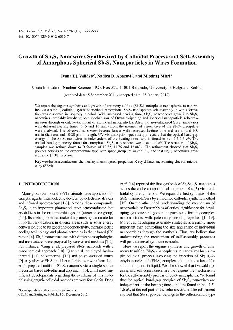
Figure 1A shows phases of colloidal synthetic route forpreparation of Sb2S3 nanowires on the time scale step bystep. The current synthetic method is a modified well-devel-oped technique for colloidal synthesis established by Denget al. by using “green” and low-cost paraffin liquid as thesolvent [23]. This technique avoids the use of TOP, as TOPis unstable, hazardous, expensive and environmentally harmfulsolvent, whereas paraffin liquid is a nontoxic, environmen-tally friendly and stable solvent with a boiling point above300 °C. The synthesis shown on Fig. 1A involves the nextstep: (A) yellow S-paraffin liquid solution at the temperatureof 240 °C, (B) orange liquid solution obtained immediatelyafter injection of Sb(III)-2-ethylhexanoic acid-complex intothe S-paraffin liquid solution, (C) red solution obtained after1 min of heating, (D) maroon solution obtained after 3 min-utes of heating and (E) gray-black solution forming after5 min of heating. It is important to emphasize here that in allthe above described solutions precipitate is present, exceptfor situation (A) where Sb(III)-2-ethylhexanoic acid-com-plex is not injected yet. The changing in color of the mixedsolution from yellow to gray-black indicated the formation ofSb2S3 species. The precipitates completely released from paraf-fin were taken from steps (B), (C) and (D) and correspond-ing SEM micrographs and XRD patterns with assignedplanes (JCPDS 03-065-2432) are shown in Fig. 1A. As canbe seen in the initial stages (B) and (C), noncrystalline anddeformed nanospheres were obtained. In stage (D) quite per-fect and homogeneous nanospheres with diameters around100 nm, with well defined diffraction peaks on the still visi-ble amorphous base, were observed. The final stage, (E),contains crystalline Sb2S3 nanowires as the end product andtheir optical and morphological dependence is the functionof the heating time we discuss further in the text.
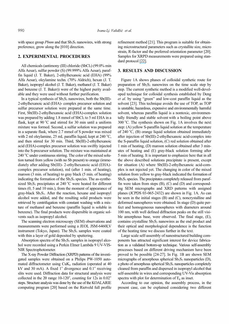
Large scale self-assembly of nanostructured building com-ponents has attracted significant interest for device fabrica-tion as a validated bottom-up technique. Various self-assemblyprocesses based on different driving mechanism have beenproved to be possible [24-27]. In Fig. 1B are shown SEMmicrographs of amorphous spherical Sb2S3 nanoparticles (D),a photo of amorphous spherical Sb2S3 nanoparticles completelycleaned from paraffin and dispersed in isopropyl alcohol thatself-assemble in wires and corresponding UV-Vis absorptionspectra with plot for determination of Eg as inset.
According to our opinion, the assembly process, in thepresent case, can be explained considering two different
Growth of Sb2S3 Nanowires Synthesized by Colloidal Process and Self-Assembly 991
growth mechanisms: (i) Ostwald-Ripening (diffusion/disso-lution) where small crystals or sol particles dissolve andredeposit onto larger crystals or sol particles, because largerparticles are more energetically favored than smaller parti-cles (see Fig. 1A (C) and (D)), based on transformation thatwe believe happened in samples (C) to (D) where we observedlarge and small nanoparticles that end up in quite regular andonly large particles, and (ii) self-organization of sphericalnanoparticles through oriented-attachment of individual nano-particles leading to the formation of nanowires (Fig. 2).Probably, after attaining some critical size by Ostwald-ripen-ing, an entire nanoparticle can act as a building block for the
crystallization by oriented-attachment. This is exactly whatwe have observed at the transition from sample (D) to (E)(SEM micrographs of nanowires observed in Sample E andfurther their dependence with increased heating time areshown in Fig. 2). It is important to emphasize here thatspherical nanoparticle diameter depicted in stage (D) corre-sponds to the nanowires diameters, a-fact that supports theoriented-attachment mechanism. The results obtained fromUV-Vis absorption spectra will be discussed further in the text.
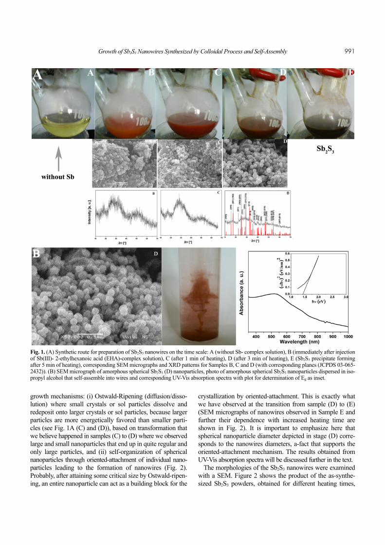
The morphologies of the Sb2S3 nanowires were examinedwith a SEM. Figure 2 shows the product of the as-synthe-sized Sb2S3 powders, obtained for different heating times,
Fig. 1. (A) Synthetic route for preparation of Sb2S3 nanowires on the time scale: A (without Sb- complex solution), B (immediately after injectionof Sb(III)- 2-ethylhexanoic acid (EHA)-complex solution), C (after 1 min of heating), D (after 3 min of heating), E (Sb2S3 precipitate formingafter 5 min of heating), corresponding SEM micrographs and XRD patterns for Samples B, C and D (with corresponding planes (JCPDS 03-065-2432)). (B) SEM micrograph of amorphous spherical Sb2S3 (D) nanoparticles, photo of amorphous spherical Sb2S3 nanoparticles dispersed in iso-propyl alcohol that self-assemble into wires and corresponding UV-Vis absorption spectra with plot for determination of Eg as inset.
992 Ivana Lj. Validži et al.c
from the moment of appearance of the Sb2S3 precipitate at240 °C, A column (0 min.), B Column (5 min.) and C col-umn (10 min.) and compared at the same magnification. Asseen in Column A, the lengths of the product range from 3 to10 µm and diameters from 80 to 120 nm. Further, ColumnsB and C show the products heated for 5 and 10 min, and con-tain nanowires that became longer with heating. The lengthsof the product range from 5 to 20 µm with diameters around100 nm. No real differences in diameters and no significantmorphological differences between the last two samplesheated for 5 and 10 min have been observed. Thus, the longerthe heating time, the longer the lengths of the produced nanow-ires. For heating time above 5 min, saturation in the nanow-ires lengths occurs. Briefly, nanowires arise and grow only in
the first 5 min from the moment of appearance of gray-blackSb2S3, while prolonged heating does not have any visibleeffects on theirs morphology.
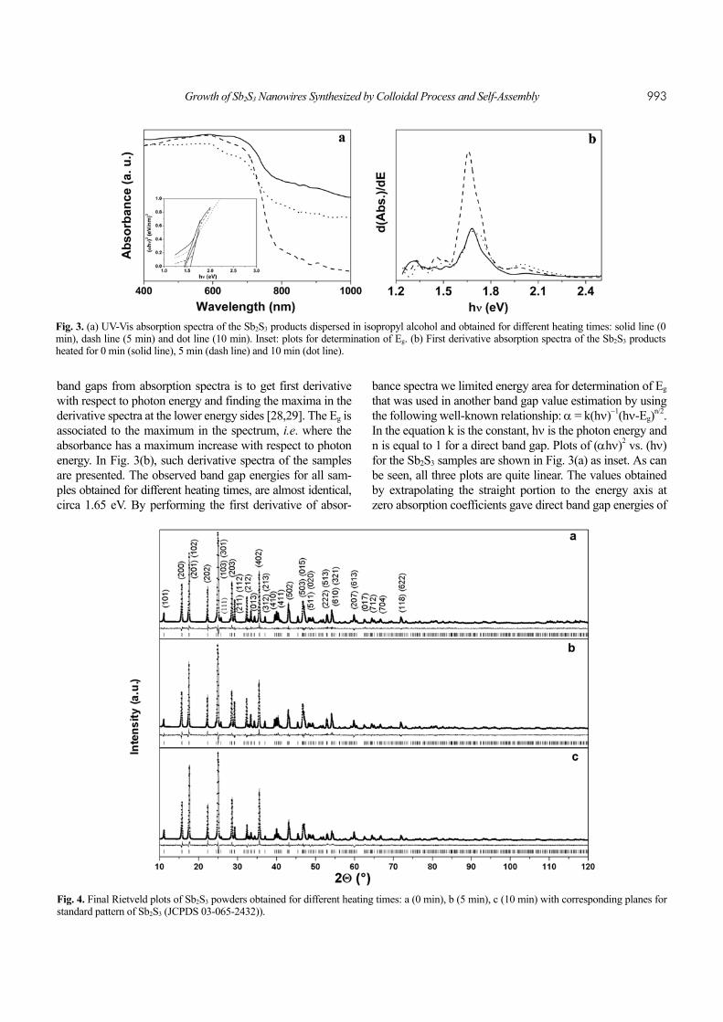
An optical absorption experiment has been carried outusing the UV-visible spectra, which provide a simple andeffective method for explaining some features concerningthe band structure. Since all experimental results, includingXRPD and SEM observations, suggest that Sb2S3 nanowiresare in pure high-quality crystalline phases, we suppose thatthe absorption spectrum represents the true absorption behaviorof Sb2S3 nanowires. Figure 3(a) shows the typical UV-visibleabsorption spectra taken from slightly turbid Sb2S3 disper-sions obtained for different heating times: a (0 min), b (5min) and c (10 min). One of the common ways of extracting
Fig. 2. SEM images of the as-synthesized Sb2S3 powders obtained for different heating times A column (0 min), B column (5 min) and C column(10 min), and compared on the same magnification.
Growth of Sb2S3 Nanowires Synthesized by Colloidal Process and Self-Assembly 993
band gaps from absorption spectra is to get first derivativewith respect to photon energy and finding the maxima in thederivative spectra at the lower energy sides [28,29]. The Eg isassociated to the maximum in the spectrum, i.e. where theabsorbance has a maximum increase with respect to photonenergy. In Fig. 3(b), such derivative spectra of the samplesare presented. The observed band gap energies for all sam-ples obtained for different heating times, are almost identical,circa 1.65 eV. By performing the first derivative of absor-
bance spectra we limited energy area for determination of Eg
that was used in another band gap value estimation by usingthe following well-known relationship: α = k(hν)−1(hν-Eg)n/2.In the equation k is the constant, hν is the photon energy andn is equal to 1 for a direct band gap. Plots of (αhν)2 vs. (hν)for the Sb2S3 samples are shown in Fig. 3(a) as inset. As canbe seen, all three plots are quite linear. The values obtainedby extrapolating the straight portion to the energy axis atzero absorption coefficients gave direct band gap energies of
Fig. 3. (a) UV-Vis absorption spectra of the Sb2S3 products dispersed in isopropyl alcohol and obtained for different heating times: solid line (0min), dash line (5 min) and dot line (10 min). Inset: plots for determination of Eg. (b) First derivative absorption spectra of the Sb2S3 productsheated for 0 min (solid line), 5 min (dash line) and 10 min (dot line).
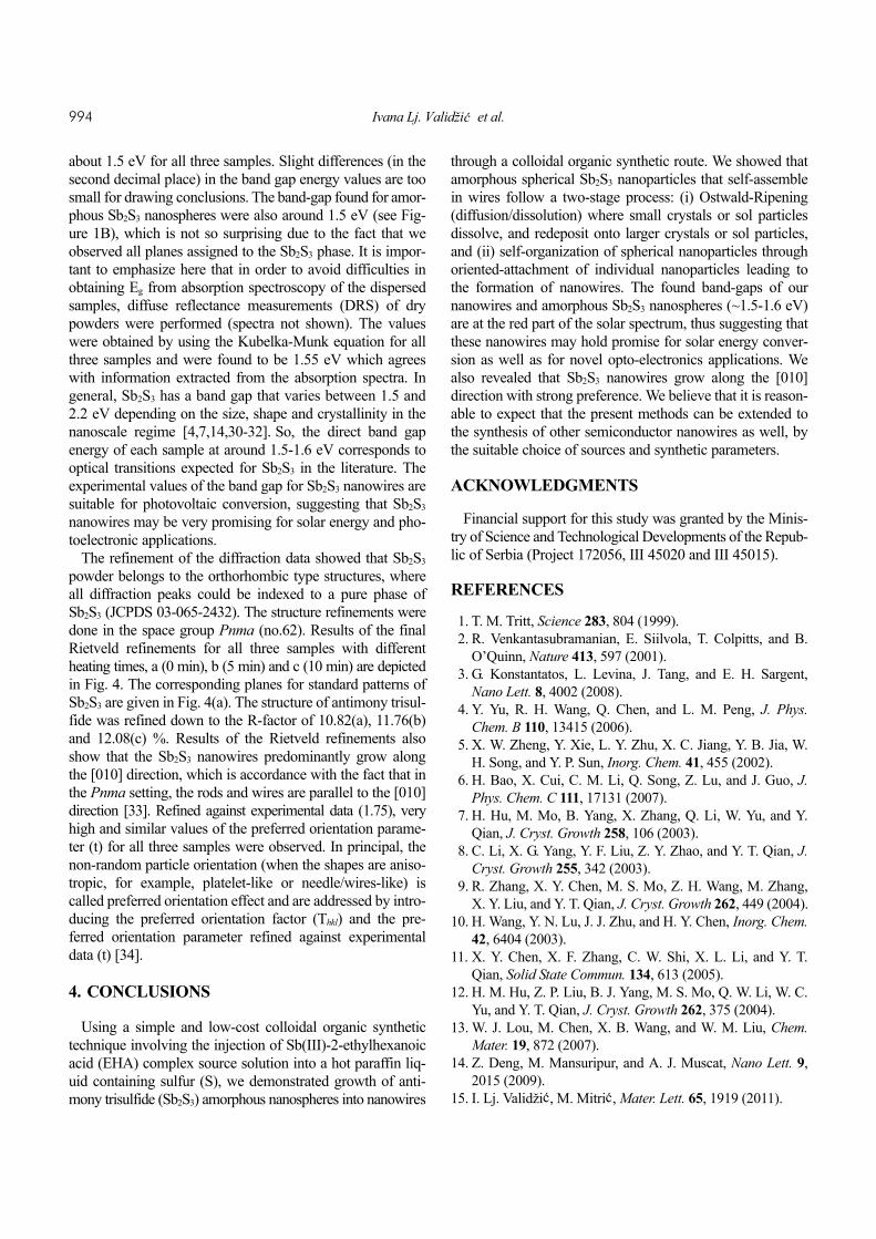
Fig. 4. Final Rietveld plots of Sb2S3 powders obtained for different heating times: a (0 min), b (5 min), c (10 min) with corresponding planes forstandard pattern of Sb2S3 (JCPDS 03-065-2432)).
994 Ivana Lj. Validži et al.c
about 1.5 eV for all three samples. Slight differences (in thesecond decimal place) in the band gap energy values are toosmall for drawing conclusions. The band-gap found for amor-phous Sb2S3 nanospheres were also around 1.5 eV (see Fig-ure 1B), which is not so surprising due to the fact that weobserved all planes assigned to the Sb2S3 phase. It is impor-tant to emphasize here that in order to avoid difficulties inobtaining Eg from absorption spectroscopy of the dispersedsamples, diffuse reflectance measurements (DRS) of drypowders were performed (spectra not shown). The valueswere obtained by using the Kubelka-Munk equation for allthree samples and were found to be 1.55 eV which agreeswith information extracted from the absorption spectra. Ingeneral, Sb2S3 has a band gap that varies between 1.5 and2.2 eV depending on the size, shape and crystallinity in thenanoscale regime [4,7,14,30-32]. So, the direct band gapenergy of each sample at around 1.5-1.6 eV corresponds tooptical transitions expected for Sb2S3 in the literature. Theexperimental values of the band gap for Sb2S3 nanowires aresuitable for photovoltaic conversion, suggesting that Sb2S3
nanowires may be very promising for solar energy and pho-toelectronic applications.
The refinement of the diffraction data showed that Sb2S3
powder belongs to the orthorhombic type structures, whereall diffraction peaks could be indexed to a pure phase ofSb2S3 (JCPDS 03-065-2432). The structure refinements weredone in the space group Pnma (no.62). Results of the finalRietveld refinements for all three samples with differentheating times, a (0 min), b (5 min) and c (10 min) are depictedin Fig. 4. The corresponding planes for standard patterns ofSb2S3 are given in Fig. 4(a). The structure of antimony trisul-fide was refined down to the R-factor of 10.82(a), 11.76(b)and 12.08(c) %. Results of the Rietveld refinements alsoshow that the Sb2S3 nanowires predominantly grow alongthe [010] direction, which is accordance with the fact that inthe Pnma setting, the rods and wires are parallel to the [010]direction [33]. Refined against experimental data (1.75), veryhigh and similar values of the preferred orientation parame-ter (t) for all three samples were observed. In principal, thenon-random particle orientation (when the shapes are aniso-tropic, for example, platelet-like or needle/wires-like) iscalled preferred orientation effect and are addressed by intro-ducing the preferred orientation factor (Thkl) and the pre-ferred orientation parameter refined against experimentaldata (t) [34].
4. CONCLUSIONS
Using a simple and low-cost colloidal organic synthetictechnique involving the injection of Sb(III)-2-ethylhexanoicacid (EHA) complex source solution into a hot paraffin liq-uid containing sulfur (S), we demonstrated growth of anti-mony trisulfide (Sb2S3) amorphous nanospheres into nanowires
through a colloidal organic synthetic route. We showed thatamorphous spherical Sb2S3 nanoparticles that self-assemblein wires follow a two-stage process: (i) Ostwald-Ripening(diffusion/dissolution) where small crystals or sol particlesdissolve, and redeposit onto larger crystals or sol particles,and (ii) self-organization of spherical nanoparticles throughoriented-attachment of individual nanoparticles leading tothe formation of nanowires. The found band-gaps of ournanowires and amorphous Sb2S3 nanospheres (~1.5-1.6 eV)are at the red part of the solar spectrum, thus suggesting thatthese nanowires may hold promise for solar energy conver-sion as well as for novel opto-electronics applications. Wealso revealed that Sb2S3 nanowires grow along the [010]direction with strong preference. We believe that it is reason-able to expect that the present methods can be extended tothe synthesis of other semiconductor nanowires as well, bythe suitable choice of sources and synthetic parameters.
ACKNOWLEDGMENTS
Financial support for this study was granted by the Minis-try of Science and Technological Developments of the Repub-lic of Serbia (Project 172056, III 45020 and III 45015).
REFERENCES
1. T. M. Tritt, Science 283, 804 (1999).2. R. Venkantasubramanian, E. Siilvola, T. Colpitts, and B.
O’Quinn, Nature 413, 597 (2001).3. G. Konstantatos, L. Levina, J. Tang, and E. H. Sargent,
Nano Lett. 8, 4002 (2008).4. Y. Yu, R. H. Wang, Q. Chen, and L. M. Peng, J. Phys.
Chem. B 110, 13415 (2006).5. X. W. Zheng, Y. Xie, L. Y. Zhu, X. C. Jiang, Y. B. Jia, W.
H. Song, and Y. P. Sun, Inorg. Chem. 41, 455 (2002).6. H. Bao, X. Cui, C. M. Li, Q. Song, Z. Lu, and J. Guo, J.
Phys. Chem. C 111, 17131 (2007).7. H. Hu, M. Mo, B. Yang, X. Zhang, Q. Li, W. Yu, and Y.
Qian, J. Cryst. Growth 258, 106 (2003).8. C. Li, X. G. Yang, Y. F. Liu, Z. Y. Zhao, and Y. T. Qian, J.
Cryst. Growth 255, 342 (2003).9. R. Zhang, X. Y. Chen, M. S. Mo, Z. H. Wang, M. Zhang,
X. Y. Liu, and Y. T. Qian, J. Cryst. Growth 262, 449 (2004).10. H. Wang, Y. N. Lu, J. J. Zhu, and H. Y. Chen, Inorg. Chem.
42, 6404 (2003). 11. X. Y. Chen, X. F. Zhang, C. W. Shi, X. L. Li, and Y. T.
Qian, Solid State Commun. 134, 613 (2005).12. H. M. Hu, Z. P. Liu, B. J. Yang, M. S. Mo, Q. W. Li, W. C.
Yu, and Y. T. Qian, J. Cryst. Growth 262, 375 (2004).13. W. J. Lou, M. Chen, X. B. Wang, and W. M. Liu, Chem.
Mater. 19, 872 (2007).14. Z. Deng, M. Mansuripur, and A. J. Muscat, Nano Lett. 9,
2015 (2009).15. I. Lj. Validži , M. Mitri , Mater. Lett. 65, 1919 (2011).c c
Growth of Sb2S3 Nanowires Synthesized by Colloidal Process and Self-Assembly 995
16. H. Colfen and S. Mann, Angew. Chem. Int. Ed. 42, 2350(2003).
17. S. I. Stupp, V. LeBonheur, K. Walker, L. S. Li, K. E. Hug-gins, M. Keser, and A. Amstutz, Science 276, 384 (1997).
18. C. B. Murray, C. R. Kagan, and M. G. Bawendi, Science270, 1335 (1995).
19. A. P. Alivisatos, Adv. Mater. 10, 1297 (1998).20. R. W. Cheary and A. A. Coehlo, J. Appl. Crystallogr. 25,
109 (1992).21. H. Rietveld, J. Appl. Crystallogr. 2, 65 (1969).22. V. K. Pecharsky and P. Y. Zavalij, Fundamentals of Powder
Diffraction and Structural Characterization of Materials,Chapter 3, pp.292-293, Springer (2005).
23. Z. Deng, L. Cao, F. Tang, and B. Zou, J. Phys. Chem. B 109,16671 (2005).
24. H. G. Yang and H. C. Zeng, J. Phys. Chem. B 108, 3492(2004).
25. Y. Yin, R. M. Rioux, C. K. Erdonmez, S. Hughes, G. A.Somorjai, and A. P. Alivisatos, Science 304, 711 (2004).
26. S. Park, J. H. Lim, S. W. Chung, and C. A. Mirkin, Science303, 348 (2004).
27. C. Pacholski, A. Kornowski, and H. Weller, Angew. Chem.114, 1234 (2002).
28. M. Becerril, H. Silva-Lopez, and O. Zelaya-Angel, Rev.Mex. Fis. 50, 588 (2004).
29. A. E. Morales, E. S. Mora, and U. Pal, Rev. Mex. Fis. S 53,18 (2007).
30. M. T. S. Nair, Y. Pena, J. Campos, V. M. Garcia, and P. K.Nair, J. Electrochem. Soc. 145, 2113 (1998).
31. J. Ota and S. K. Srivastava, Cryst. Growth Des. 7, 343 (2007).32. J. Yang, J. H. Zeng, S. H. Yu, L. Yang, Y. H. Zhang, and Y.
T. Qian, Chem. Mater. 12, 2924 (2000).33. L. F. Lundegaard, R. Miletich, T. Balic-Zunic, and E. Mak-
ovicky, Phys. Chem. Minerals 30, 463 (2003).34. V. K. Pecharsky and P. Y. Zavalij, Fundamentals of Powder
Diffraction and Structural Characterization of Materials,Chapter 8, pp.194-199, Springer (2009).


