Embed Size (px)
Citation preview
H plasma cleaning and a-Si passivation of GaAs for surface channeldevice applications
C. Marchiori,a� D. J. Webb, C. Rossel, M. Richter, M. Sousa, C. Gerl, R. Germann,C. Andersson, and J. FompeyrineIBM Research-Zurich, 8803 Rüschlikon, Switzerland
�Received 31 July 2009; accepted 17 October 2009; published online 10 December 2009�
We discuss GaAs�001� cleaning and surface passivation for metal-oxide-semiconductor capacitorsand field effect transistors fabricated with HfO2 as high-� gate oxide. An amorphous-Si passivatinglayer is deposited by molecular beam deposition on a 2�1 reconstructed GaAs surface cleanedusing a remote rf H plasma. The H plasma effectively removes C contaminants from the surface, buta progressive Ga enrichment and the presence of Ga–O bonds are observed. The capacitance-voltagemeasurements on capacitors under peripheral illumination show inversion, which is an indication ofa passivated interface. The Dit distribution as function of energy in the band gap is extracted byusing the conductance technique at high and low temperatures and is reported for HfO2 /a-Si gatestacks on H-cleaned GaAs. The observed Dit distribution is asymmetric. Values as low as 7�1011 eV−1 cm−1 are found in the upper half of the band gap. One clear peak at 0.7 eV and a tailat 0.2 eV above the valence band maximum, which can be part of a second peak, are also observed.Transistor data confirm that a conducting channel is effectively opened at or very close to the GaAssurface. © 2009 American Institute of Physics. �doi:10.1063/1.3260251�
I. INTRODUCTION
One of the most important issues to be solved in order tofabricate effective inversion mode, surface channel metal-oxide-semiconductor field effect transistors �MOSFETs� onIII-V substrates is the Fermi-level �FL� pinning, which isusually observed at the dielectric/semiconductor interface.According to the advanced unified defect model,1 the FL ispinned by defect levels induced by the formation of Ga or Asantisites in the GaAs near-surface region. Ga and As dis-placement with formation of antisites may be caused by Asor Ga excess, reaction with metals or adsorption of contami-nants such as O2 on the free GaAs surface.2 The only way toovercome the problem is then to develop efficient GaAscleaning and passivating methods.
In this paper, we study the electrical properties of MOScapacitors and transistors fabricated on GaAs�001� substratescleaned in H plasma and passivated by a thin layer of amor-phous Si.
With respect to other in situ cleaning methods, H plasmaoffers the advantage of being effective at low substrate tem-peratures. This greatly reduces group V desorption and con-sequently surface roughening. H plasma etching may there-fore be employed to clean preprocessed patterned substratesthat cannot withstand the standard oxide desorption in Asoverpressure. This may be especially useful for the cointe-gration of III-V MOS devices with other semiconductors.Substantial improvements in the electrical properties of MOScapacitors have been observed by Callegari3 and Clark4
when the GaAs surface had been treated in H plasma prior toinsulator deposition. However, systematic studies on theGaAs surface composition after H treatment were not per-formed on those structures. In this respect, there have been
many reports of contrasting results �As-rich, Ga-rich, etc�.In addition, among different passivating approaches for
the clean GaAs surface, i.e., molecular beam deposition�MBD� of Ga2O3–Gd2O3,5 sulfur,6 and atomic layer deposi-tion of Al2O3,7 the use of an amorphous, thin Si layer seemsto be particularly promising. Si also passivates Ge surfacesefficiently, which is an additional advantage from the per-spective of the cointegration of III-V and Ge MOS devices.Si-passivated GaAs capacitors with good electricalproperties8,9 were reported recently, and working surfacechannel transistors10,11 with high mobility have been fabri-cated. Nevertheless, a detailed investigation of the passivat-ing efficiency of MBD Si has yet to be done. We present herean approach that takes advantage of the fact that cleaning,passivating, and deposition steps are all performed in UHV.
II. EXPERIMENTAL
p- and n-type GaAs�001� epiready wafers were firstdipped in a 1% HF solution in H2O in order to remove partof the oxides and subsequently rinsed in de-ionized water.Afterwards, they were dried and loaded into a DCA MBEcluster system consisting of three MBE integrated chambers:one for III-V growth, one for Si/Ge, and one for oxide depo-sition. Prior to Si deposition, the wafers were exposed to aremote atomic H plasma to remove any residual oxide. Therf H plasma was operated at 600 W rf power at a chamberpressure of 1�10−5 Torr. During H exposure, the substratewas heated to 250 °C. The optical emission of the H plasmawas monitored and kept constant between different runs.Owing to a special source design and the use of electrostaticdeflection plates, only the neutral species effuse into the pro-cess chamber. Therefore, substrate damage due to the plasmais not expected. The cleaning process was monitored withreflection high-energy electron diffraction �RHEED� and ina�Electronic mail: [email protected].
JOURNAL OF APPLIED PHYSICS 106, 114112 �2009�
0021-8979/2009/106�11�/114112/8/$25.00 © 2009 American Institute of Physics106, 114112-1
situ x-ray photoelectron spectroscopy �XPS�. Si and high-�deposition were performed by e-beam evaporation from el-emental Si and Hf. Si passivating layers 1.5–2 nm thick weregrown at a deposition rate of 6 Å/min. The chamber residualpressure during e-beam evaporation ranged from 3�10−8 Torr to 5�10−7 Torr, while the substrate was keptat room temperature. Successively, 7 nm thick layers of HfO2
were deposited by Hf evaporation in O plasma onto the sub-strate heated to 250 °C. A metal deposition rate of 3 Å/minwas employed in O plasma for a chamber pressure of 1�10−5 Torr.
In situ XPS analysis was performed in a contiguouschamber with a base pressure of 1.5�10−9 Torr, equippedwith a monochromatic Al K� x-ray source and two Phoi-bos150 analyzers �CHA� at take off angles of 20° and 50°with respect to the normal to the sample surface. Spectrawere taken with pass energy values of 30 and 10 eV for themore energy-resolved spectra. Fits were always attemptedwith a minimum number of components.
For As and Ga bulk doublets, the spin orbit splitting wasfixed at �BE=0.7 eV and �BE=0.44 eV, respectively, witha branching ratio of 2:3. The fitted widths of the oxide peakswere adjustable parameters. They were constrained to a com-mon value in a given spectrum, which could be 0.3–0.5 eVlarger than the bulk doublets but never more than twice, asdiscussed by Landgren et al.12 It should be mentioned thatthe detection limit of XPS corresponds to about 0.01 ML�monolayer� at the top surface.
In order to make capacitors for electrical measurements,the wafers were cleaved into pieces, which were annealed at700 °C in N2 for 5 s. Al was evaporated through a shadow-mask as top electrode. The thickness of the gate electrodeensured that, under illumination, the semiconductor area be-low the gate is not exposed to light. The backsides of thepieces were scratched and glued using a Ga/In alloy to a Cuplate to make the back contact. Capacitance–voltage �CV�measurements in parallel mode were performed in the darkor with illumination of the dot periphery, using an AgilentLCR meter �4284A�. The frequencies f of the ac signal were0.1, 1, 10 and 100 kHz. White light was used to perform CVmeasurements under peripheral illumination.
Ring MOSFETs have been made on semi-insulating �un-doped� GaAs with a gate first process. A 200 nm thick layerof W was used as a gate metal and also as the implantationmask for source and drain implantations of the Si dopants.The activation annealing were done in N2. AuGeNiAu met-allization was used for the source and drain contact metalsand alloyed at 380 °C for 60 s in an ArH2 mixture.
III. SURFACE CLEANING
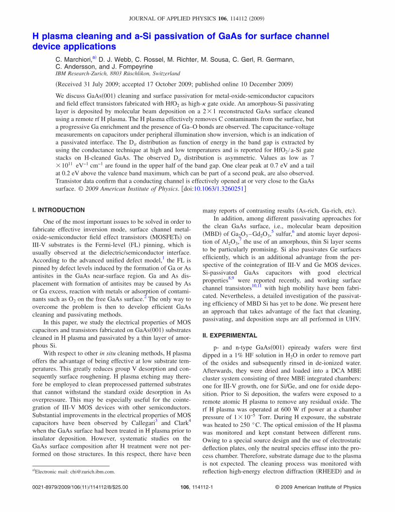
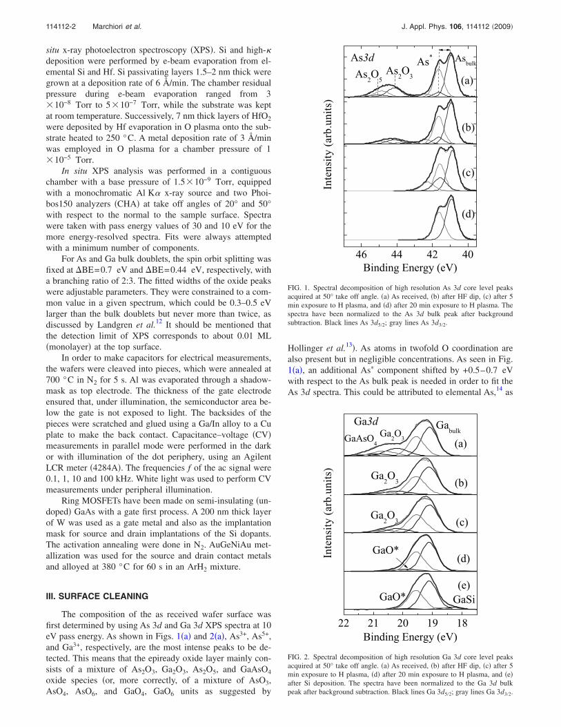
The composition of the as received wafer surface wasfirst determined by using As 3d and Ga 3d XPS spectra at 10eV pass energy. As shown in Figs. 1�a� and 2�a�, As3+, As5+,and Ga3+, respectively, are the most intense peaks to be de-tected. This means that the epiready oxide layer mainly con-sists of a mixture of As2O3, Ga2O3, As2O5, and GaAsO4
oxide species �or, more correctly, of a mixture of AsO3,AsO4, AsO6, and GaO4, GaO6 units as suggested by
Hollinger et al.13�. As atoms in twofold O coordination arealso present but in negligible concentrations. As seen in Fig.1�a�, an additional As� component shifted by +0.5–0.7 eVwith respect to the As bulk peak is needed in order to fit theAs 3d spectra. This could be attributed to elemental As,14 as
FIG. 1. Spectral decomposition of high resolution As 3d core level peaksacquired at 50° take off angle. �a� As received, �b� after HF dip, �c� after 5min exposure to H plasma, and �d� after 20 min exposure to H plasma. Thespectra have been normalized to the As 3d bulk peak after backgroundsubtraction. Black lines As 3d5/2; gray lines As 3d3/2.
FIG. 2. Spectral decomposition of high resolution Ga 3d core level peaksacquired at 50° take off angle. �a� As received, �b� after HF dip, �c� after 5min exposure to H plasma, �d� after 20 min exposure to H plasma, and �e�after Si deposition. The spectra have been normalized to the Ga 3d bulkpeak after background subtraction. Black lines Ga 3d5/2; gray lines Ga 3d3/2.
114112-2 Marchiori et al. J. Appl. Phys. 106, 114112 �2009�
expected from thermodynamical calculations on GaAs oxi-dation. On the other hand, this spectral contribution mayoriginate from the presence of As–O bonds, as observed byLandgren et al.,12 who explained that the As 3d spectralcomponent shifted by +0.8 eV implies the formation of Asatoms with onefold O coordination.
Furthermore, the C 1s spectrum �not shown� exhibitstwo peaks, at 284.5 and 285.9 eV, which indicates that rela-tively large amounts of adsorbed hydrocarbons and alcoholsgroups, respectively, are present on the surface of theepiready oxide.
The same fitting procedures were used to follow thevariation in the different chemical species and their oxidationstates after the different cleaning steps, as shown in Figs.1�b�–1�d� and 2�b�–2�d�. As 3d, Ga 3d, O 1s, and C 1s spec-tra were also used for quantifications; the following quanti-ties were taken into account.
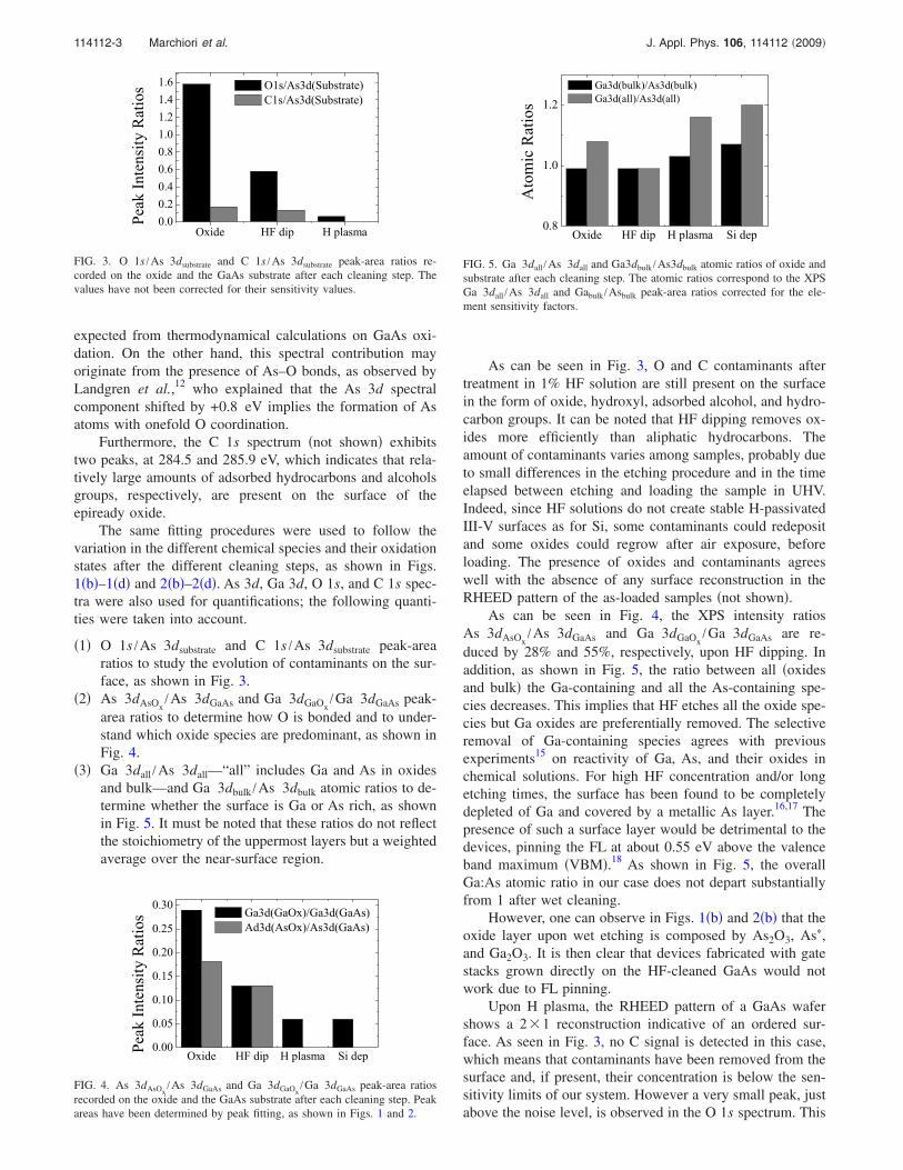
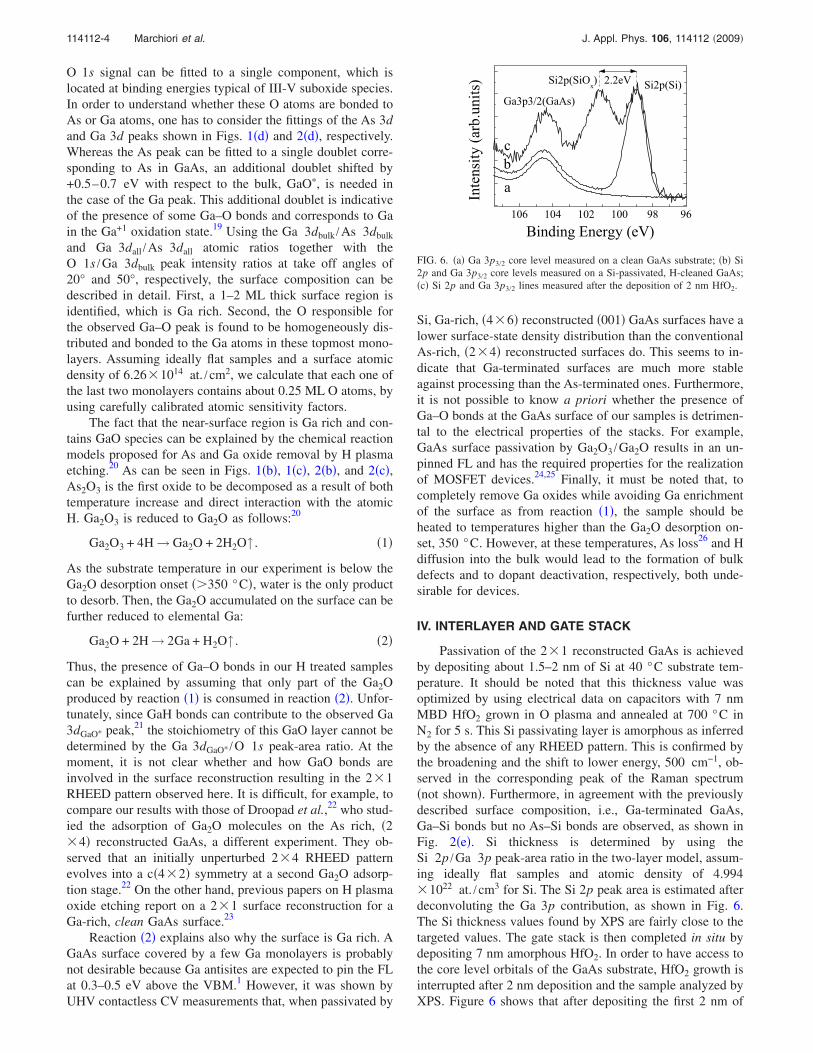
�1� O 1s /As 3dsubstrate and C 1s /As 3dsubstrate peak-arearatios to study the evolution of contaminants on the sur-face, as shown in Fig. 3.
�2� As 3dAsOx/As 3dGaAs and Ga 3dGaOx
/Ga 3dGaAs peak-area ratios to determine how O is bonded and to under-stand which oxide species are predominant, as shown inFig. 4.
�3� Ga 3dall /As 3dall—“all” includes Ga and As in oxidesand bulk—and Ga 3dbulk /As 3dbulk atomic ratios to de-termine whether the surface is Ga or As rich, as shownin Fig. 5. It must be noted that these ratios do not reflectthe stoichiometry of the uppermost layers but a weightedaverage over the near-surface region.
As can be seen in Fig. 3, O and C contaminants aftertreatment in 1% HF solution are still present on the surfacein the form of oxide, hydroxyl, adsorbed alcohol, and hydro-carbon groups. It can be noted that HF dipping removes ox-ides more efficiently than aliphatic hydrocarbons. Theamount of contaminants varies among samples, probably dueto small differences in the etching procedure and in the timeelapsed between etching and loading the sample in UHV.Indeed, since HF solutions do not create stable H-passivatedIII-V surfaces as for Si, some contaminants could redepositand some oxides could regrow after air exposure, beforeloading. The presence of oxides and contaminants agreeswell with the absence of any surface reconstruction in theRHEED pattern of the as-loaded samples �not shown�.
As can be seen in Fig. 4, the XPS intensity ratiosAs 3dAsOx
/As 3dGaAs and Ga 3dGaOx/Ga 3dGaAs are re-
duced by 28% and 55%, respectively, upon HF dipping. Inaddition, as shown in Fig. 5, the ratio between all �oxidesand bulk� the Ga-containing and all the As-containing spe-cies decreases. This implies that HF etches all the oxide spe-cies but Ga oxides are preferentially removed. The selectiveremoval of Ga-containing species agrees with previousexperiments15 on reactivity of Ga, As, and their oxides inchemical solutions. For high HF concentration and/or longetching times, the surface has been found to be completelydepleted of Ga and covered by a metallic As layer.16,17 Thepresence of such a surface layer would be detrimental to thedevices, pinning the FL at about 0.55 eV above the valenceband maximum �VBM�.18 As shown in Fig. 5, the overallGa:As atomic ratio in our case does not depart substantiallyfrom 1 after wet cleaning.
However, one can observe in Figs. 1�b� and 2�b� that theoxide layer upon wet etching is composed by As2O3, As�,and Ga2O3. It is then clear that devices fabricated with gatestacks grown directly on the HF-cleaned GaAs would notwork due to FL pinning.
Upon H plasma, the RHEED pattern of a GaAs wafershows a 2�1 reconstruction indicative of an ordered sur-face. As seen in Fig. 3, no C signal is detected in this case,which means that contaminants have been removed from thesurface and, if present, their concentration is below the sen-sitivity limits of our system. However a very small peak, justabove the noise level, is observed in the O 1s spectrum. This
FIG. 3. O 1s /As 3dsubstrate and C 1s /As 3dsubstrate peak-area ratios re-corded on the oxide and the GaAs substrate after each cleaning step. Thevalues have not been corrected for their sensitivity values.
FIG. 4. As 3dAsOx/As 3dGaAs and Ga 3dGaOx
/Ga 3dGaAs peak-area ratiosrecorded on the oxide and the GaAs substrate after each cleaning step. Peakareas have been determined by peak fitting, as shown in Figs. 1 and 2.
FIG. 5. Ga 3dall /As 3dall and Ga3dbulk /As3dbulk atomic ratios of oxide andsubstrate after each cleaning step. The atomic ratios correspond to the XPSGa 3dall /As 3dall and Gabulk /Asbulk peak-area ratios corrected for the ele-ment sensitivity factors.
114112-3 Marchiori et al. J. Appl. Phys. 106, 114112 �2009�
O 1s signal can be fitted to a single component, which islocated at binding energies typical of III-V suboxide species.In order to understand whether these O atoms are bonded toAs or Ga atoms, one has to consider the fittings of the As 3dand Ga 3d peaks shown in Figs. 1�d� and 2�d�, respectively.Whereas the As peak can be fitted to a single doublet corre-sponding to As in GaAs, an additional doublet shifted by+0.5–0.7 eV with respect to the bulk, GaO�, is needed inthe case of the Ga peak. This additional doublet is indicativeof the presence of some Ga–O bonds and corresponds to Gain the Ga+1 oxidation state.19 Using the Ga 3dbulk /As 3dbulk
and Ga 3dall /As 3dall atomic ratios together with theO 1s /Ga 3dbulk peak intensity ratios at take off angles of20° and 50°, respectively, the surface composition can bedescribed in detail. First, a 1–2 ML thick surface region isidentified, which is Ga rich. Second, the O responsible forthe observed Ga–O peak is found to be homogeneously dis-tributed and bonded to the Ga atoms in these topmost mono-layers. Assuming ideally flat samples and a surface atomicdensity of 6.26�1014 at. /cm2, we calculate that each one ofthe last two monolayers contains about 0.25 ML O atoms, byusing carefully calibrated atomic sensitivity factors.
The fact that the near-surface region is Ga rich and con-tains GaO species can be explained by the chemical reactionmodels proposed for As and Ga oxide removal by H plasmaetching.20 As can be seen in Figs. 1�b�, 1�c�, 2�b�, and 2�c�,As2O3 is the first oxide to be decomposed as a result of bothtemperature increase and direct interaction with the atomicH. Ga2O3 is reduced to Ga2O as follows:20
Ga2O3 + 4H → Ga2O + 2H2O↑ . �1�
As the substrate temperature in our experiment is below theGa2O desorption onset ��350 °C�, water is the only productto desorb. Then, the Ga2O accumulated on the surface can befurther reduced to elemental Ga:
Ga2O + 2H → 2Ga + H2O↑ . �2�
Thus, the presence of Ga–O bonds in our H treated samplescan be explained by assuming that only part of the Ga2Oproduced by reaction �1� is consumed in reaction �2�. Unfor-tunately, since GaH bonds can contribute to the observed Ga3dGaO� peak,21 the stoichiometry of this GaO layer cannot bedetermined by the Ga 3dGaO� /O 1s peak-area ratio. At themoment, it is not clear whether and how GaO bonds areinvolved in the surface reconstruction resulting in the 2�1RHEED pattern observed here. It is difficult, for example, tocompare our results with those of Droopad et al.,22 who stud-ied the adsorption of Ga2O molecules on the As rich, �2�4� reconstructed GaAs, a different experiment. They ob-served that an initially unperturbed 2�4 RHEED patternevolves into a c�4�2� symmetry at a second Ga2O adsorp-tion stage.22 On the other hand, previous papers on H plasmaoxide etching report on a 2�1 surface reconstruction for aGa-rich, clean GaAs surface.23
Reaction �2� explains also why the surface is Ga rich. AGaAs surface covered by a few Ga monolayers is probablynot desirable because Ga antisites are expected to pin the FLat 0.3–0.5 eV above the VBM.1 However, it was shown byUHV contactless CV measurements that, when passivated by
Si, Ga-rich, �4�6� reconstructed �001� GaAs surfaces have alower surface-state density distribution than the conventionalAs-rich, �2�4� reconstructed surfaces do. This seems to in-dicate that Ga-terminated surfaces are much more stableagainst processing than the As-terminated ones. Furthermore,it is not possible to know a priori whether the presence ofGa–O bonds at the GaAs surface of our samples is detrimen-tal to the electrical properties of the stacks. For example,GaAs surface passivation by Ga2O3 /Ga2O results in an un-pinned FL and has the required properties for the realizationof MOSFET devices.24,25 Finally, it must be noted that, tocompletely remove Ga oxides while avoiding Ga enrichmentof the surface as from reaction �1�, the sample should beheated to temperatures higher than the Ga2O desorption on-set, 350 °C. However, at these temperatures, As loss26 and Hdiffusion into the bulk would lead to the formation of bulkdefects and to dopant deactivation, respectively, both unde-sirable for devices.
IV. INTERLAYER AND GATE STACK
Passivation of the 2�1 reconstructed GaAs is achievedby depositing about 1.5–2 nm of Si at 40 °C substrate tem-perature. It should be noted that this thickness value wasoptimized by using electrical data on capacitors with 7 nmMBD HfO2 grown in O plasma and annealed at 700 °C inN2 for 5 s. This Si passivating layer is amorphous as inferredby the absence of any RHEED pattern. This is confirmed bythe broadening and the shift to lower energy, 500 cm−1, ob-served in the corresponding peak of the Raman spectrum�not shown�. Furthermore, in agreement with the previouslydescribed surface composition, i.e., Ga-terminated GaAs,Ga–Si bonds but no As–Si bonds are observed, as shown inFig. 2�e�. Si thickness is determined by using theSi 2p /Ga 3p peak-area ratio in the two-layer model, assum-ing ideally flat samples and atomic density of 4.994�1022 at. /cm3 for Si. The Si 2p peak area is estimated afterdeconvoluting the Ga 3p contribution, as shown in Fig. 6.The Si thickness values found by XPS are fairly close to thetargeted values. The gate stack is then completed in situ bydepositing 7 nm amorphous HfO2. In order to have access tothe core level orbitals of the GaAs substrate, HfO2 growth isinterrupted after 2 nm deposition and the sample analyzed byXPS. Figure 6 shows that after depositing the first 2 nm of
FIG. 6. �a� Ga 3p3/2 core level measured on a clean GaAs substrate; �b� Si2p and Ga 3p3/2 core levels measured on a Si-passivated, H-cleaned GaAs;�c� Si 2p and Ga 3p3/2 lines measured after the deposition of 2 nm HfO2.
114112-4 Marchiori et al. J. Appl. Phys. 106, 114112 �2009�
HfO2, the Si is only partially oxidized: the passivating layer,initially 1.9�0.2 nm thick, consists now of 1.2�0.2 nmelemental Si and about 0.8�0.2 nm oxidized species. How-ever, these oxidized species do not correspond to SiO2 but toSi suboxides, SiOx, as can be inferred by the 2.2 eV bindingenergy shift of the Si 2pSiO peak with respect to the bulk Si2p peak �Fig. 6�. It should be noted that, even if Si is onlypartially oxidized to SiOx, Hf is fully oxidized in the HfO2
overlayer and no signs of Hf silicide are detected. Finally,after depositing the remaining 5 nm HfO2 and annealing, thefinal gate stack composition is found by spectroscopic ellip-sometry to be 6.4 nm HfO2 /2.3 nm HfSixOy /0.2 nmSiO2 /0.3 nm Si. The Si thickness has been reduced so as toavoid parallel conduction while hindering GaAs oxidation atthe same time.
V. ELECTRICAL PROPERTIES
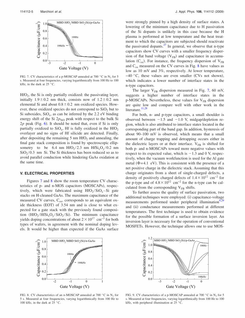
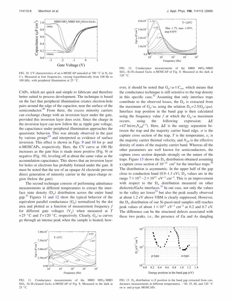
Figures 7 and 8 show the room temperature CV charac-teristics of p- and n-MOS capacitors �MOSCAPs�, respec-tively, which were fabricated using HfO2 /SiOx–Si gatestacks on H-cleaned GaAs. The maximum capacitance of themeasured CV curves, Cox, corresponds to an equivalent ox-ide thickness �EOT� of 3.54 nm and is close to what ex-pected for a gate stack with the previously found composi-tion �HfO2 /HfSixOy /SiO2 /Si�. The minimum capacitanceyields doping concentrations of about 2�1017 cm−3 for bothtypes of wafers, in agreement with the nominal doping lev-els. It would be higher than expected if the GaAs surface
were strongly pinned by a high density of surface states. Alowering of the minimum capacitance due to H passivationof the Si dopants is unlikely in this case because the Hplasma is performed at low temperature and the heat treat-ment to which the capacitors are subjected should reactivatethe passivated dopants.27 In general, we observe that n-typecapacitors show CV curves with a smaller frequency disper-sion of flat band voltage �VFB� and capacitance in accumu-lation �Cox�. For instance, the frequency dispersion of VFB
and Cox measured on the CV curves in Fig. 8 have values aslow as 10 mV and 3%, respectively. At lower temperature,−40 °C, these values are even smaller �CVs not shown�,which indicates a lower number of interface states in then-type capacitors.
The larger VFB dispersion measured in Fig. 7, 60 mV,suggests a higher number of interface states in thep-MOSCAPs. Nevertheless, these values for VFB dispersionare quite low and compare well with other work in theliterature.11,28
For both, n- and p-type capacitors, a small shoulder isobserved between �1.5 and �1.0 V, midgap/depletion re-gion, which is also attributed to interface states located in thecorresponding part of the band gap. In addition, hysteresis ofabout 90–100 mV is observed, which means that a smallamount of charge trapping and detrapping occurs either inthe dielectric layers or at their interface. VFB is shifted forboth p- and n-MOSCAPs toward more negative values withrespect to its expected value, which is �1.3 and 0 V, respec-tively, when the vacuum workfunction is used for the Al gatemetal ��=4.1 eV�. This is consistent with the presence of anet positive charge in the dielectric stack. Assuming that thischarge originates from a sheet of single-charged defects, adensity of positively charged defects of 1.4�1012 cm−2 forthe p-type and of 4.8�1012 cm−2 for the n-type can be cal-culated from the corresponding VFB shifts.
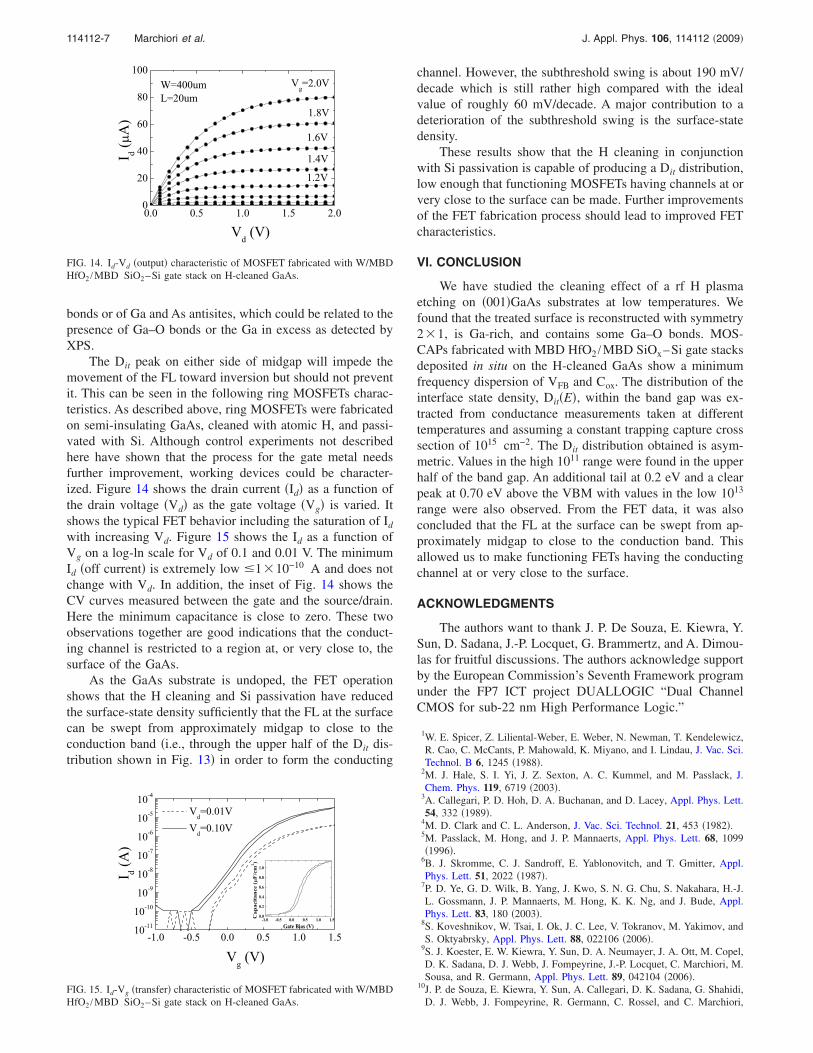
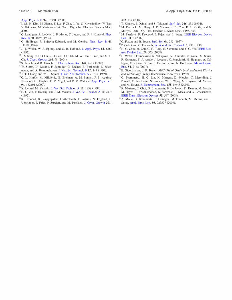
To further assess the quality of surface passivation, twoadditional techniques were employed: �i� capacitance-voltagemeasurements performed under peripheral illumination9,29
and �ii� conductance measurements performed at differenttemperatures. The first technique is used to obtain evidencefor the possible formation of a surface inversion layer. Aninversion layer is necessary for the operation of conventionalMOSFETs. However, the technique allows one to use MOS-
FIG. 9. CV characteristics of a p-MOSCAP annealed at 700 °C in N2 for 5s. Measured at four frequencies, varying logarithmically from 100 Hz to 100kHz, with peripheral illumination at 25 °C.
FIG. 7. CV characteristics of a p-MOSCAP annealed at 700 °C in N2 for 5s. Measured at four frequencies, varying logarithmically from 100 Hz to 100kHz, in the dark at 25 °C.
FIG. 8. CV characteristics of an n-MOSCAP annealed at 700 °C in N2 for5 s. Measured at four frequencies, varying logarithmically from 100 Hz to100 kHz, in the dark at 25 °C.
114112-5 Marchiori et al. J. Appl. Phys. 106, 114112 �2009�
CAPs, which are quick and simple to fabricate and thereforebetter suited to process development. The technique is basedon the fact that peripheral illumination creates electron-holepairs around the edge of the capacitor, near the surface of thesemiconductor.30 From there, the excess minority carrierscan exchange charge with an inversion layer under the gate,provided this inversion layer does exist. Since the charge inthe inversion layer can now follow the ac ripple gate voltage,the capacitance under peripheral illumination approaches thequasistatic behavior. This was already observed in the pastby various groups4,9 and interpreted as evidence of surfaceinversion. This effect is shown in Figs. 9 and 10 for p- andn-MOSCAPs, respectively. Here, the CV curve at 100 Hzincreases as the gate bias is made more positive �Fig. 9� ornegative �Fig. 10�, leveling off at about the same value as theaccumulation capacitance. This shows that an inversion layerfor holes or electrons has probably formed under the gate. Itmust be noted that the use of an opaque Al electrode preventdirect generation of minority carrier in the space-charge re-gion �below the gate�.
The second technique consists of performing admittancemeasurements at different temperatures to extract the inter-face state density �Dit� distribution across the entire bandgap.31 Figures 11 and 12 show the typical behavior of theequivalent parallel conductance �Gp� normalized by the dotarea and plotted as a function of measurement frequency ffor different gate voltages �Vg� when measured at T=25 °C and T=120 °C, respectively. Clearly, Gp / curvesgo through an intense peak when the sample is heated; how-
ever, it should be noted that Gp /Cox, which means thatthe conductance technique is still sensitive to the trap densityin this specific case.32 Assuming that only interface trapscontribute to the observed losses, the Dit is extracted fromthe maximum of Gp /, using the relation Dit=2.5�Gp /q�.Interface trap position in the band gap is then calculatedusing the frequency value f at which the Gp / maximumoccurs, using the following expression: �E=kT ln��vtNefff
−1�. Here, �E is the energy separation be-tween the trap and the majority carrier band edge, � is thecapture cross section of the trap, T is the temperature, vt isthe majority carrier thermal velocity, and Neff is the effectivedensity of states of the majority carrier band. Whereas all theother parameters are well known for semiconductors, thecapture cross section depends strongly on the nature of thetraps. Figure 13 shows the Dit distribution obtained assuminga capture cross section of 10−15 cm2 for the interface traps.24
The distribution is asymmetric. In the upper half of the gapclose to conduction band �0.9–1.3 eV�, Dit values are in therange 7�1011–2�1012 eV−1 cm−2. This is an improvementwith respect to the Dit distribution measured on otherdielectric/GaAs interfaces.31 In our case, not only the valuesin the valley are lower33 but also the peak usually observedat about 1.2 eV above VBM is clearly suppressed. However,the Dit distribution of our Si-passivated samples still reachespeak values of about 1�1013 eV−1 cm−2 at 0.2 and 0.7 eV.The difference can be the structural defects associated withthese two peaks, i.e., the presence of Ga and As dangling
FIG. 10. CV characteristics of an n-MOSCAP annealed at 700 °C in N2 for5 s. Measured at four frequencies, varying logarithmically from 100 Hz to100 kHz, with peripheral illumination at 25 °C.
FIG. 11. Conductance measurements of the MBD HfO2 /MBDSiOx–Si /H-cleaned GaAs n-MOSCAP of Fig. 8. Measured in the dark at25 °C.
FIG. 12. Conductance measurements of the MBD HfO2 /MBDSiOx–Si /H-cleaned GaAs n-MOSCAP of Fig. 8. Measured in the dark at120 °C.
FIG. 13. Dit distribution vs E position in the band gap extracted from con-ductance measurements at different temperatures, �40, 25, 60, and 120 °Con n- and p-type MOSCAPs.
114112-6 Marchiori et al. J. Appl. Phys. 106, 114112 �2009�
bonds or of Ga and As antisites, which could be related to thepresence of Ga–O bonds or the Ga in excess as detected byXPS.
The Dit peak on either side of midgap will impede themovement of the FL toward inversion but should not preventit. This can be seen in the following ring MOSFETs charac-teristics. As described above, ring MOSFETs were fabricatedon semi-insulating GaAs, cleaned with atomic H, and passi-vated with Si. Although control experiments not describedhere have shown that the process for the gate metal needsfurther improvement, working devices could be character-ized. Figure 14 shows the drain current �Id� as a function ofthe drain voltage �Vd� as the gate voltage �Vg� is varied. Itshows the typical FET behavior including the saturation of Id
with increasing Vd. Figure 15 shows the Id as a function ofVg on a log-ln scale for Vd of 0.1 and 0.01 V. The minimumId �off current� is extremely low 1�10−10 A and does notchange with Vd. In addition, the inset of Fig. 14 shows theCV curves measured between the gate and the source/drain.Here the minimum capacitance is close to zero. These twoobservations together are good indications that the conduct-ing channel is restricted to a region at, or very close to, thesurface of the GaAs.
As the GaAs substrate is undoped, the FET operationshows that the H cleaning and Si passivation have reducedthe surface-state density sufficiently that the FL at the surfacecan be swept from approximately midgap to close to theconduction band �i.e., through the upper half of the Dit dis-tribution shown in Fig. 13� in order to form the conducting
channel. However, the subthreshold swing is about 190 mV/decade which is still rather high compared with the idealvalue of roughly 60 mV/decade. A major contribution to adeterioration of the subthreshold swing is the surface-statedensity.
These results show that the H cleaning in conjunctionwith Si passivation is capable of producing a Dit distribution,low enough that functioning MOSFETs having channels at orvery close to the surface can be made. Further improvementsof the FET fabrication process should lead to improved FETcharacteristics.
VI. CONCLUSION
We have studied the cleaning effect of a rf H plasmaetching on �001�GaAs substrates at low temperatures. Wefound that the treated surface is reconstructed with symmetry2�1, is Ga-rich, and contains some Ga–O bonds. MOS-CAPs fabricated with MBD HfO2 /MBD SiOx–Si gate stacksdeposited in situ on the H-cleaned GaAs show a minimumfrequency dispersion of VFB and Cox. The distribution of theinterface state density, Dit�E�, within the band gap was ex-tracted from conductance measurements taken at differenttemperatures and assuming a constant trapping capture crosssection of 1015 cm−2. The Dit distribution obtained is asym-metric. Values in the high 1011 range were found in the upperhalf of the band gap. An additional tail at 0.2 eV and a clearpeak at 0.70 eV above the VBM with values in the low 1013
range were also observed. From the FET data, it was alsoconcluded that the FL at the surface can be swept from ap-proximately midgap to close to the conduction band. Thisallowed us to make functioning FETs having the conductingchannel at or very close to the surface.
ACKNOWLEDGMENTS
The authors want to thank J. P. De Souza, E. Kiewra, Y.Sun, D. Sadana, J.-P. Locquet, G. Brammertz, and A. Dimou-las for fruitful discussions. The authors acknowledge supportby the European Commission’s Seventh Framework programunder the FP7 ICT project DUALLOGIC “Dual ChannelCMOS for sub-22 nm High Performance Logic.”
1W. E. Spicer, Z. Liliental-Weber, E. Weber, N. Newman, T. Kendelewicz,R. Cao, C. McCants, P. Mahowald, K. Miyano, and I. Lindau, J. Vac. Sci.Technol. B 6, 1245 �1988�.
2M. J. Hale, S. I. Yi, J. Z. Sexton, A. C. Kummel, and M. Passlack, J.Chem. Phys. 119, 6719 �2003�.
3A. Callegari, P. D. Hoh, D. A. Buchanan, and D. Lacey, Appl. Phys. Lett.54, 332 �1989�.
4M. D. Clark and C. L. Anderson, J. Vac. Sci. Technol. 21, 453 �1982�.5M. Passlack, M. Hong, and J. P. Mannaerts, Appl. Phys. Lett. 68, 1099�1996�.
6B. J. Skromme, C. J. Sandroff, E. Yablonovitch, and T. Gmitter, Appl.Phys. Lett. 51, 2022 �1987�.
7P. D. Ye, G. D. Wilk, B. Yang, J. Kwo, S. N. G. Chu, S. Nakahara, H.-J.L. Gossmann, J. P. Mannaerts, M. Hong, K. K. Ng, and J. Bude, Appl.Phys. Lett. 83, 180 �2003�.
8S. Koveshnikov, W. Tsai, I. Ok, J. C. Lee, V. Tokranov, M. Yakimov, andS. Oktyabrsky, Appl. Phys. Lett. 88, 022106 �2006�.
9S. J. Koester, E. W. Kiewra, Y. Sun, D. A. Neumayer, J. A. Ott, M. Copel,D. K. Sadana, D. J. Webb, J. Fompeyrine, J.-P. Locquet, C. Marchiori, M.Sousa, and R. Germann, Appl. Phys. Lett. 89, 042104 �2006�.
10J. P. de Souza, E. Kiewra, Y. Sun, A. Callegari, D. K. Sadana, G. Shahidi,D. J. Webb, J. Fompeyrine, R. Germann, C. Rossel, and C. Marchiori,
FIG. 14. Id-Vd �output� characteristic of MOSFET fabricated with W/MBDHfO2 /MBD SiO2–Si gate stack on H-cleaned GaAs.
FIG. 15. Id-Vg �transfer� characteristic of MOSFET fabricated with W/MBDHfO2 /MBD SiO2–Si gate stack on H-cleaned GaAs.
114112-7 Marchiori et al. J. Appl. Phys. 106, 114112 �2009�
Appl. Phys. Lett. 92, 153508 �2008�.11I. Ok, H. Kim, M. Zhang, T. Lee, F. Zhu, L. Yu, S. Koveshnikov, W. Tsai,
V. Tokranov, M. Yakimov et al., Tech. Dig. - Int. Electron Devices Meet.2006, 1.
12G. Landgren, R. Ludeke, J. F. Morar, Y. Jugnet, and F. J. Himpsel, Phys.Rev. B 30, 4839 �1984�.
13G. Hollinger, R. Skheyta-Kabbani, and M. Gendry, Phys. Rev. B 49,11159 �1994�.
14J. T. Wolan, W. S. Epling, and G. B. Hoflund, J. Appl. Phys. 81, 6160�1997�.
15J. S. Song, Y. C. Choi, S. H. Seo, D. C. Oh, M. W. Cho, T. Yao, and M. H.Oh, J. Cryst. Growth 264, 98 �2004�.
16S. Adachi and D. Kikuchi, J. Electrochem. Soc. 147, 4618 �2000�.17W. Storm, D. Wolany, F. Schroder, G. Becker, B. Burkhardt, L. Wied-
mann, and A. Benninghoven, J. Vac. Sci. Technol. B 12, 147 �1994�.18T. T. Chiang and W. E. Spicer, J. Vac. Sci. Technol. A 7, 724 �1989�.19C. L. Hinkle, M. Milojevic, B. Brennan, A. M. Sonnet, F. S. Aguirre-
Tostado, G. J. Hughes, E. M. Vogel, and R. M. Wallace, Appl. Phys. Lett.94, 162101 �2009�.
20Y. Ide and M. Yamada, J. Vac. Sci. Technol. A 12, 1858 �1994�.21E. J. Petit, F. Houzay, and J. M. Moison, J. Vac. Sci. Technol. A 10, 2172
�1992�.22R. Droopad, K. Rajagopalan, J. Abrokwah, L. Adams, N. England, D.
Uebelhoer, P. Fejes, P. Zurcher, and M. Passlack, J. Cryst. Growth 301–
302, 139 �2007�.23T. Kikawa, I. Ochiai, and S. Takatani, Surf. Sci. 316, 238 �1994�.24M. Passlack, M. Hong, J. P. Mannaerts, S. Chu, R. L. Opila, and N.
Moriya, Tech. Dig. - Int. Electron Devices Meet. 1995, 383.25M. Passlack, R. Droopad, P. Fejes, and L. Wang, IEEE Electron Device
Lett. 30, 2 �2009�.26C. Foxon and B. Joyce, Surf. Sci. 64, 293 �1977�.27P. Collot and C. Gaonach, Semicond. Sci. Technol. 5, 237 �1990�.28H.-C. Chin, M. Zhu, C.-H. Tung, G. Samudra, and Y.-C. Yeo, IEEE Elec-
tron Device Lett. 29, 553 �2008�.29D. Webb, J. Fompeyrine, S. Nakagawa, A. Dimoulas, C. Rossel, M. Sousa,
R. Germann, S. Alvarado, J. Locquet, C. Marchiori, H. Siegwart, A. Cal-legari, E. Kiewra, Y. Sun, J. De Souza, and N. Hoffmann, Microelectron.Eng. 84, 2142 �2007�.
30E. Nicollian and J. R. Brews, MOS (Metal Oxide Semiconductor) Physicsand Technology �Wiley-Interscience, New York, 1982�.
31G. Brammertz, H. C. Lin, K. Martens, D. Mercier, C. Merckling, J.Penaud, C. Adelmann, S. Sioncke, W. E. Wang, M. Caymax, M. Meuris,and M. Heyns, J. Electrochem. Soc. 155, H945 �2008�.
32K. Martens, C. Chui, G. Brammertz, B. De Jaeger, D. Kuzum, M. Meuris,M. Heyns, T. Krishnamohan, K. Saraswat, H. Maes, and G. Groeseneken,IEEE Trans. Electron Devices 55, 547 �2008�.
33A. Molle, G. Brammertz, L. Lamagna, M. Fanciulli, M. Meuris, and S.Spiga, Appl. Phys. Lett. 95, 023507 �2009�.
114112-8 Marchiori et al. J. Appl. Phys. 106, 114112 �2009�


