Embed Size (px)
Citation preview
HEART RATE MONITOR &TEMPERATURE MEASURING DEVICE
B.Tech. MINI Project Report
HRUSHIKESH.P.V.R.R RANJAN.H.R
SRI HARSHA.U
DEPARTMENT OF BIO-MEDICAL ENGINEERING
GOKARAJU RANGARAJU INSTITUTE OF ENGINEERING AND TECHNOLOGY
(Affiliated to Jawaharlal Nehru Technological University)
HYDERABAD 500 090
2010
HEART RATE MONITOR &TEMPERATURE
MEASURING DEVICE Project Report Submitted in Partial Fulfillment of
the Requirements for the Degree of
Bachelor of Technology
in
BioMedical Engineering by
HRUSHIKESH.P.V.R.R (Roll.No. 07241A1112) RANJAN.H.R(Roll.No. 07241A1124)
SRI HARSHA.U (Roll.No. 07241A1129)
DEPARTMENT OF BIO-MEDICAL ENGINEERING
GOKARAJU RANGARAJU INSTITUTE OF ENGINEERING AND TECHNOLOGY
(Affiliated to Jawaharlal Nehru Technological University)
HYDERABAD 500 090
2010
Department of BioMedical Engineering
Gokaraju Rangaraju Institute of Engineering and Technology
(Affiliated to Jawaharlal Nehru Technological University)
Hyderabad 500 090
2010
Certificate
This is to certify that this project report entitled HEART RATE MONITOR &TEMPERATURE MEASURING DEVICE by HRUSHIKESH.P.V.R.R (Roll No.07241A1112), RANJAN.H.R (Roll No.07241A1124), SRI HARSHA.U (Roll No.07241A1129) submitted in partial fulfillment of the requirements for the degree of Bachelor of Technology in BioMedical Engineering of the Jawaharlal Nehru Technological University, Hyderabad, during the academic year 2010, is a bonafide record of work carried out under our guidance and supervision.
The results embodied in this report have not been submitted to any other University or
Institution for the award of any degree or diploma.
(Guide) (External Examiner) (Head of Department) D.Swathi T.Padma Assistant Professor

A C K N O W L E D G E M E N T There are many people who have helped us directly or indirectly in the successful
completion of our project. We would like to take this opportunity to thank one and all.
First of all we would like to express our deep sense of gratitude towards our project Guide Ms
Swathi.D Asst Professor Dept. of BME for always being available whenever we require her
guidance as well as for motivating us through out the project work.
We are also grateful to the Mrs T.Padma, (Head of Dept.of BME for her valuable guidance
during our project. We would like to express our deep gratitude towards our teaching and non-
teaching staff for giving their valuable suggestions and co operation sfor doing our project.
We are also deeply indebted to Dr. Jandhyala. N. Murthy, Principal, Gokaraju
Rangaraju institute of engineering and technology for providing necessary facilities during the
execution of this project.
We would like to thank all our friends for their help and constructive criticism during our project
period. Finally, we are very much indebted to our parents for their moral support and encouragement to
achieve higher goals. we have no words to express our gratitude and still we are very thankful to our
parents who have shown us this world and for every support they gave us.
Signature Signature Signature
Hrushikesh.P.V.R.R Ranjan.H.R. Sri harsha.U (07241A1112) (07241A1124) (07241A1129)
CONTENTS
ABSTRACT
1. INTRODUCTION
2. CIRCUIT DIAGRAM
3. COMPONENTS DESCRIPTION
4. CIRCUIT EXPLANATION
5. MICRO CONTROLLER PROGRAMMING
6. APPLICATIONS
7. CONCLUSION
ABSTRACT
This is an attempt made which describes the design of a simple, low-cost
microcontroller based heart rate measuring device with LCD output. Heart rate of the subject is
measured from the finger by placing the thumb in between the LDR and LED and the rate is
then averaged and displayed on a text based LCD. It also consists of a temperature sensor which
is integrated with the same microcontroller and is placed between the two fingers to find the
temperature inside the human body. Both the heart rate and temperature can be known at a time
other which is very advantageous to anybody.
1.INTRODUCTION
A heart rate monitor is a personal monitoring device that allows a subject to measure their heart
rate in real time or record their heart rate for later study. Early models consisted of a monitoring
box with a set of electrode leads that attached to the chest.
Heart rate measurement is one of the very important parameters of the human cardiovascular
system. The heart rate of a healthy adult at rest is around 72 beats per minute (bpm). Athletes
normally have lower heart rates than less active people. Babies have a much higher heart rate at
around 120 bpm, while older children have heart rates at around 90 bpm. The heart rate rises
gradually during exercises and returns slowly to the rest value after exercise. The rate when the
pulse returns to normal is an indication of the fitness of the person. Lower than normal heart
rates are usually an indication of a condition known as bradycardia, while higher than normal
heart rates are known as tachycardia.
Heart rate is simply and traditionally measured by placing the thumb over the subject’s arterial
pulsation, and feeling, timing and counting the pulses usually in a 30 second period. Heart rate
(bpm) of the subject is then found by multiplying the obtained number by 2. This method
although simple, is not accurate and can give errors when the rate is high. More sophisticated
methods to measure the heart rate utilize electronic techniques. Electro-cardiogram (ECG) is one
of frequently used and accurate methods for measuring the heart rate. ECG is an expensive
device and its use for the measurement of the heart rate only is not economical. Low-cost devices
in the form of wrist watches are also available for the instantaneous measurement of the heart
rate. Such devices can give accurate measurements but their cost is usually in excess of several
hundred dollars, making them uneconomical. Most hospitals and clinics in the UK use integrated
devices designed to measure the heart rate . So this heart rate monitor with a temperature sensor
is definitely a useful instrument in knowing the pulse and the temperature of the subject or the
patient.
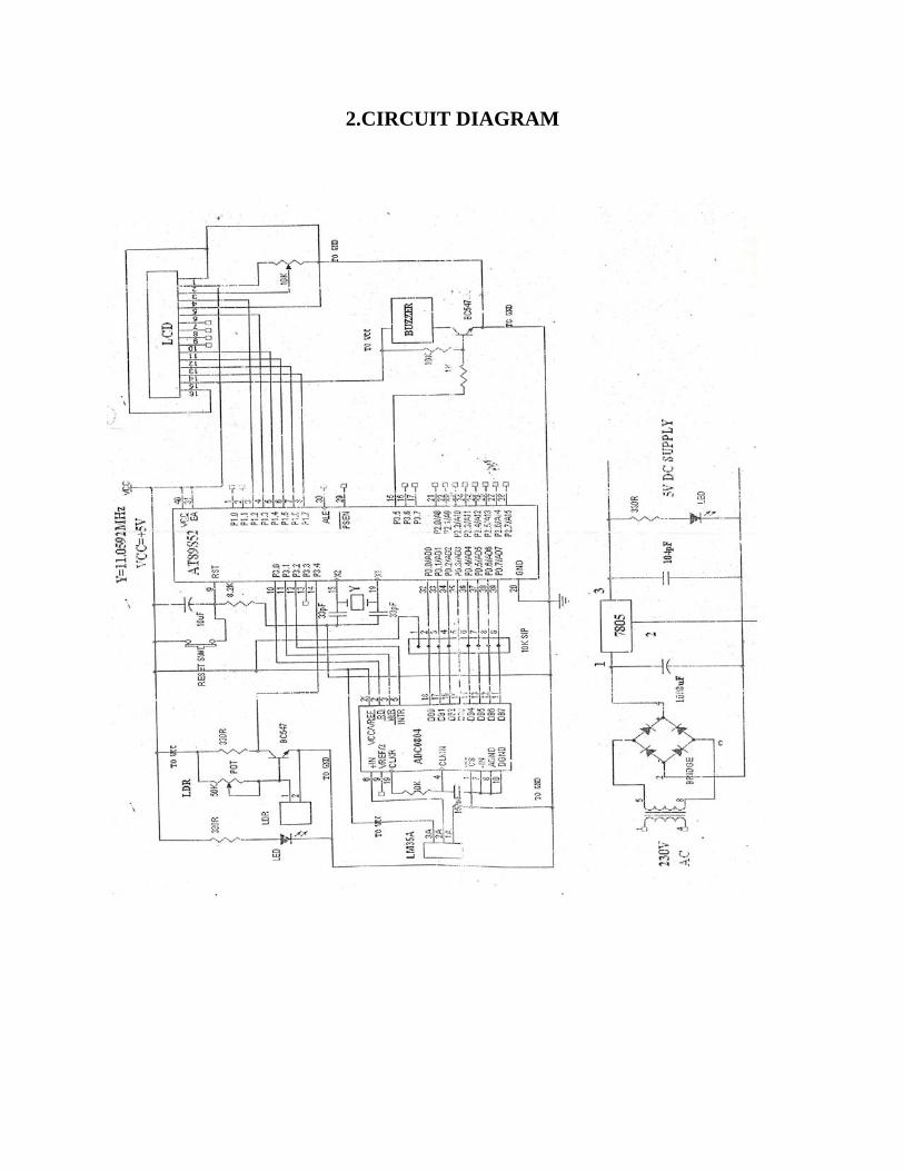
2.CIRCUIT DIAGRAM
3. COMPONENTS DESCRIPTION
There are a number of components in this module and they are as follows:
1. Micro controller-AT89S52
2. A/D Converter-ADC0804
3. Temperature sensor-LM35A
4. LCD Display
5. Buzzer
6. Reset switch
7. LDR
8. LED
9. 10K SIP
10. Potentiometer-50K
11. Transistors-BC547
12. Capacitors-15pF,33pF,104pF,10uF,1000uF
13. Resistors-1K,8.2K,10K,330K
14. Voltage regulator-7805
15. 5v DC supply
Now let us discuss about each of the component:
Micro controller-AT89S52:
Description: The AT89S52 is a low-power, high-performance CMOS 8-bit microcontroller with
8K bytes of in-system programmable Flash memory. The device is manufactured using Atmel’s
high-density nonvolatile memory technology and is compatible with the indus-try-standard
80C51 instruction set and pinout. The on-chip Flash allows the program memory to be
reprogrammed in-system or by a conventional nonvolatile memory pro-grammer. By combining
a versatile 8-bit CPU with in-system programmable Flash on a monolithic chip, the Atmel
AT89S52 is a powerful microcontroller which provides a highly-flexible and cost-effective
solution to many embedded control applications. The AT89S52 provides the following standard
features: 8K bytes of Flash, 256 bytes of RAM, 32 I/O lines, Watchdog timer, two data pointers,
three 16-bit timer/counters, a six-vector two-level interrupt architecture, a full duplex serial port,
on-chip oscillator, and clock circuitry. In addition, the AT89S52 is designed with static logic for
operation down to zero frequency and supports two software selectable power saving modes. The
Idle Mode stops the CPU while allowing the RAM, timer/counters, serial port, and interrupt
system to continue functioning. The Power-down mode saves the RAM con-tents but freezes the
oscillator, disabling all other chip functions until the next interrupt or hardware reset.
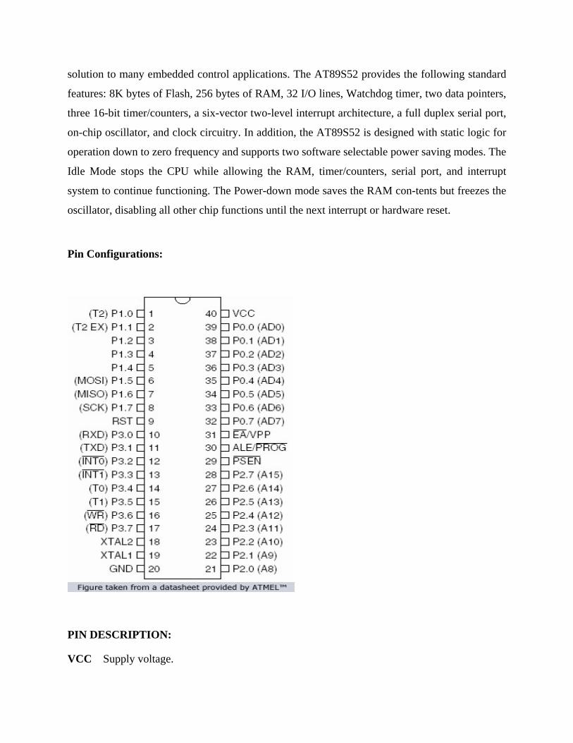
Pin Configurations:
PIN DESCRIPTION:
VCC Supply voltage.

GND Ground.
Port 0 Port 0 is an 8-bit open drain bidirectional I/O port. As an output port, each pin can sink
eight TTL inputs. When 1s are written to port 0 pins, the pins can be used as high-impedance
inputs. Port 0 can also be configured to be the multiplexed low-order address/data bus during
accesses to external program and data memory. In this mode, P0 has internal pull-ups. Port 0 also
receives the code bytes during Flash programming and outputs the code bytes dur-ing program
verification. External pull-ups are required during program verification.
Port 1 Port 1 is an 8-bit bidirectional I/O port with internal pull-ups. The Port 1 output buffers
can sink/source four TTL inputs. When 1s are written to Port 1 pins, they are pulled high by the
inter-nal pull-ups and can be used as inputs. As inputs, Port 1 pins that are externally being
pulled low will source current (IIL) because of the internal pull-ups. In addition, P1.0 and P1.1
can be configured to be the timer/counter 2 external count input (P1.0/T2) and the timer/counter
2 trigger input (P1.1/T2EX), respectively, as shown in the follow-ing table. Port 1 also receives
the low-order address bytes during Flash programming and verification.
Port Pin Alternate Functions
P1.0 - T2 (external count input to Timer/Counter 2), clock-out
P1.1 - T2EX (Timer/Counter 2 capture/reload trigger and direction control)
P1.5 - MOSI (used for In-System Programming)
P1.6 - MISO (used for In-System Programming)
P1.7 - SCK (used for In-System Programming)
Port 2 Port 2 is an 8-bit bidirectional I/O port with internal pull-ups. The Port 2 output buffers
can sink/source four TTL inputs. When 1s are written to Port 2 pins, they are pulled high by the
inter-nal pull-ups and can be used as inputs. As inputs, Port 2 pins that are externally being
pulled low will source current (IIL) because of the internal pull-ups. Port 2 emits the high-order
address byte during fetches from external program memory and dur-ing accesses to external data
memory that use 16-bit addresses (MOVX @ DPTR). In this application, Port 2 uses strong
internal pull-ups when emitting 1s. During accesses to external data memory that use 8-bit

addresses (MOVX @ RI), Port 2 emits the contents of the P2 Special Function Register. Port 2
also receives the high-order address bits and some control signals during Flash program-ming
and verification.
Port 3 Port 3 is an 8-bit bidirectional I/O port with internal pull-ups. The Port 3 output buffers
can sink/source four TTL inputs. When 1s are written to Port 3 pins, they are pulled high by the
inter-nal pull-ups and can be used as inputs. As inputs, Port 3 pins that are externally being
pulled low will source current (IIL) because of the pull-ups. Port 3 receives some control signals
for Flash programming and verification. Port 3 also serves the functions of various special
features of the AT89S52, as shown in the fol-lowing table.
Port Pin Alternate Functions
P3.0 - RXD (serial input port)
P3.1 - TXD (serial output port)
P3.2 - INT0 (external interrupt 0)
P3.3 - INT1 (external interrupt 1)
P3.4 - T0 (timer 0 external input)
P3.5 - T1 (timer 1 external input)
P3.6 - WR (external data memory write strobe)
P3.7 - RD (external data memory read strobe)
RST Reset input. A high on this pin for two machine cycles while the oscillator is running resets
the device. This pin drives high for 98 oscillator periods after the Watchdog times out. The
DISRTO bit in SFR AUXR (address 8EH) can be used to disable this feature. In the default state
of bit DISRTO, the RESET HIGH out feature is enabled.
ALE/PROG Address Latch Enable (ALE) is an output pulse for latching the low byte of the
address during accesses to external memory. This pin is also the program pulse input (PROG)
during Flash programming. In normal operation, ALE is emitted at a constant rate of 1/6 the
oscillator frequency and may be used for external timing or clocking purposes. Note, however,

that one ALE pulse is skipped dur-ing each access to external data memory. If desired, ALE
operation can be disabled by setting bit 0 of SFR location 8EH. With the bit set, ALE is active
only during a MOVX or MOVC instruction. Otherwise, the pin is weakly pulled high. Setting the
ALE-disable bit has no effect if the microcontroller is in external execution mode.
PSEN Program Store Enable (PSEN) is the read strobe to external program memory. When the
AT89S52 is executing code from external program memory, PSEN is activated twice each
machine cycle, except that two PSEN activations are skipped during each access to exter-nal data
memory.
EA/VPP External Access Enable. EA must be strapped to GND in order to enable the device to
fetch code from external program memory locations starting at 0000H up to FFFFH. Note,
however, that if lock bit 1 is programmed, EA will be internally latched on reset. EA should be
strapped to VCC for internal program executions. This pin also receives the 12-volt
programming enable voltage (VPP) during Flash programming.
XTAL1 Input to the inverting oscillator amplifier and input to the internal clock operating
circuit.
XTAL2 Output from the inverting oscillator amplifier.
REGISTERS:
Special Function Registers A map of the on-chip memory area called the Special Function
Register (SFR) space is shown . Note that not all of the addresses are occupied, and unoccupied
addresses may not be imple-mented on the chip. Read accesses to these addresses will in general
return random data, and write accesses will have an indeterminate effect. User software should
not write 1s to these unlisted locations, since they may be used in future products to invoke new
features. In that case, the reset or inactive values of the new bits will always be 0.
Timer 2 Registers: Control and status bits are contained in registers T2CON (shown in Table 5-
2) and T2MOD (shown in Table 10-2) for Timer 2. The register pair (RCAP2H, RCAP2L) are
the Capture/Reload registers for Timer 2 in 16-bit capture mode or 16-bit auto-reload mode.
Interrupt Registers: The individual interrupt enable bits are in the IE register. Two priorities
can be set for each of the six interrupt sources in the IP register.
Dual Data Pointer Registers: To facilitate accessing both internal and external data memory,
two banks of 16-bit Data Pointer Registers are provided: DP0 at SFR address locations 82H-83H
and DP1 at 84H-85H. Bit DPS = 0 in SFR AUXR1 selects DP0 and DPS = 1 selects DP1. The
user should ALWAYS initialize the DPS bit to the appropriate value before accessing the
respective Data Pointer Register.
Power Off Flag: The Power Off Flag (POF) is located at bit 4 (PCON.4) in the PCON SFR.
POF is set to “1” during power up. It can be set and rest under software control and is not
affected by reset.
Memory Organization
MCS-51 devices have a separate address space for Program and Data Memory. Up to 64K bytes
each of external Program and Data Memory can be addressed.
Program Memory If the EA pin is connected to GND, all program fetches are directed to
external memory. On the AT89S52, if EA is connected to VCC, program fetches to addresses
0000H through 1FFFH are directed to internal memory and fetches to addresses 2000H through
FFFFH are to external memory.
Data Memory The AT89S52 implements 256 bytes of on-chip RAM. The upper 128 bytes
occupy a parallel address space to the Special Function Registers. This means that the upper 128
bytes have the same addresses as the SFR space but are physically separate from SFR space.
When an instruction accesses an internal location above address 7FH, the address mode used in
the instruction specifies whether the CPU accesses the upper 128 bytes of RAM or the SFR
space. Instructions which use direct addressing access the SFR space. For example, the following
direct addressing instruction accesses the SFR at location 0A0H (which is P2). MOV 0A0H,
#data Instructions that use indirect addressing access the upper 128 bytes of RAM. For example,
the following indirect addressing instruction, where R0 contains 0A0H, accesses the data byte at
address 0A0H, rather than P2 (whose address is 0A0H). MOV @R0, #data Note that stack
operations are examples of indirect addressing, so the upper 128 bytes of data RAM are available
as stack space.
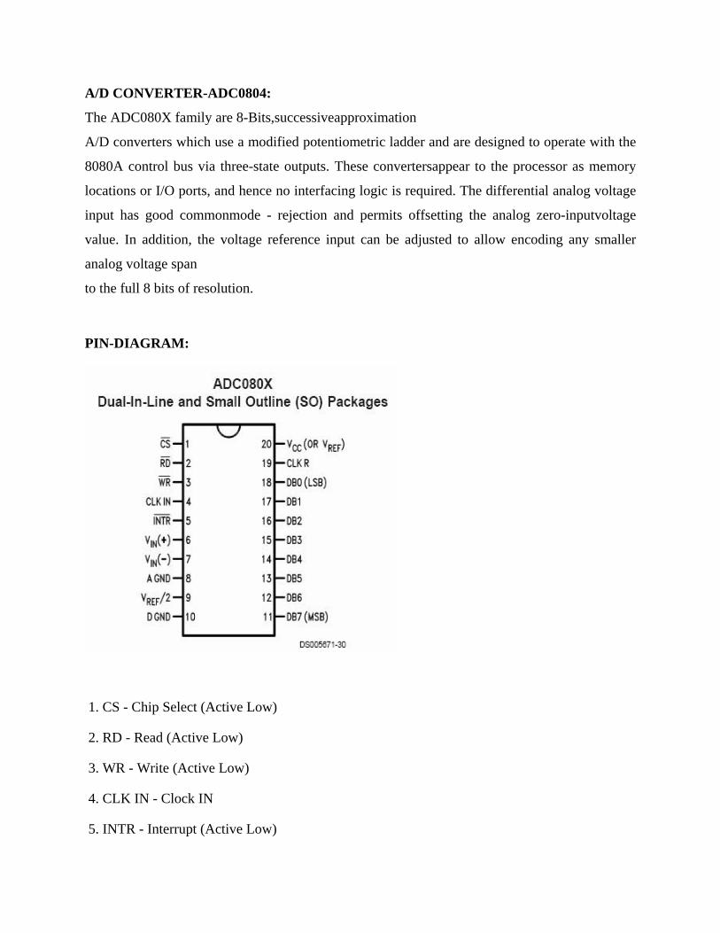
A/D CONVERTER-ADC0804:
The ADC080X family are 8-Bits,successiveapproximation
A/D converters which use a modified potentiometric ladder and are designed to operate with the
8080A control bus via three-state outputs. These convertersappear to the processor as memory
locations or I/O ports, and hence no interfacing logic is required. The differential analog voltage
input has good commonmode - rejection and permits offsetting the analog zero-inputvoltage
value. In addition, the voltage reference input can be adjusted to allow encoding any smaller
analog voltage span
to the full 8 bits of resolution.
PIN-DIAGRAM:
1. CS - Chip Select (Active Low)
2. RD - Read (Active Low)
3. WR - Write (Active Low)
4. CLK IN - Clock IN
5. INTR - Interrupt (Active Low)
6. Vin+ - Analog Voltage Input
7. Vin- - Analog Voltage Input
8. AGND - Analog Ground
9. Vref/2 - Voltage Reference / 2
10. DGND - Digital Ground
11. DB7 - Data Bit 7 (MSB)
12. DB6 - Data Bit 6
13. DB5 - Data Bit 5
14. DB4 - Data Bit 4
15. DB3 - Data Bit 3
16. DB2 - Data Bit 2
17. DB1 - Data Bit 1
18. DB0 - Data Bit 0 (LSB)
19. CLKR - Clock Reset
20. Vcc - Positive Supply or Vref
Absolute Maximum Ratings Thermal Information
Supply Voltage: 6.5V
Voltage at Any Input: -0.3V to (V+ +0.3V)
Operating Conditions
Temperature Range: 0 C to 70 C
Thermal Resistance (Typical, Note 1) �JA (oC/W)
PDIP Package : 80
Maximum Junction Temperature Plastic Package :150oC
Maximum Storage Temperature Range: -65oC to 150oC
Maximum Lead Temperature (Soldering, 10s):300oC
TEMPERATURE SENSOR-LM35A:
The LM35 series are precision integrated-circuit temperature sensors, whose output voltage is
linearly proportional to the Celsius (Centigrade) temperature. The LM35 thus has an advantage
over linear temperature sensors calibrated in ° Kelvin, as the user is not required to subtract a
large constant voltage from its output to obtain convenient Centigrade scaling. The LM35 does
not require any external calibration or trimming to provide typical accuracies of ± 1/4°C at room
temperature and ± 3/4°C over a full -55 to +150°C temperature range.
Low cost is assured by trimming and calibration at the wafer level. The LM35's low output
impedance, linear output, and precise inherent calibration make interfacing to readout or control
circuitry especially easy. It can be used with single power supplies, or with plus and minus
supplies. As it draws only 60 µA from its supply, it has very low self-heating, less than 0.1°C in
still air. The LM35 is rated to operate over a -55° to +150°C temperature range, while the
LM35C is rated for a -40° to +110°C range (-10° with improved accuracy). The LM35 series is
available packaged in hermetic TO-46 transistor packages, while the LM35C, LM35CA, and
LM35D are also available in the plastic TO-92 transistor package. The LM35D is also available
in an 8-lead surface mount small outline package and a plastic TO-220 package.
Features
Calibrated directly in ° Celsius (Centigrade) Linear + 10.0 mV/°C scale factor 0.5°C accuracy
guaranteeable (at +25°C) Rated for full -55° to +150°C range Suitable for remote applications
Low cost due to wafer-level trimming Operates from 4 to 30 volts Less than 60 µA current drain
Low self-heating, 0.08°C in still air Nonlinearity only ± 1/4°C typical Low impedance output,
0.1 for 1ma load, typical Applications DS005516-4 DS005516-3 FIGURE1.Basic Centigrade
Temperature Sensor(+2°Cto+150°C) Choose R1 = -VS/50 µA V OUT = +1,500 mV at +150°C
= +250mVat+25°C=-550mVat-55°C
FIGURE 2. Full-Range Centigrade Temperature Sensor
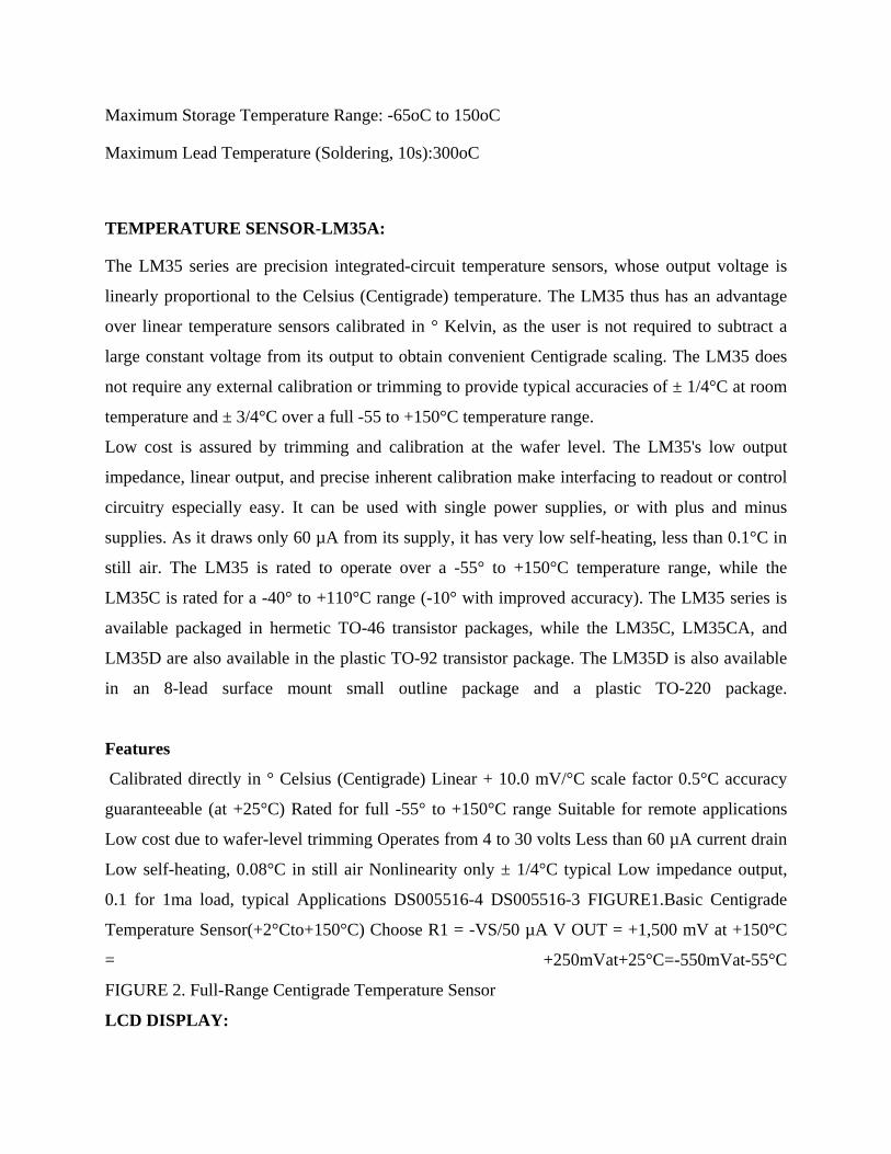
LCD DISPLAY:
A liquid crystal display (LCD) is a thin, flat electronic visual display that uses the light
modulating properties of liquid crystals (LCs). LCs do not emit light directly.
They are used in a wide range of applications including: computer monitors, television,
instrument panels, aircraft cockpit displays, signage, etc. They are common in consumer devices
such as video players, gaming devices, clocks, watches, calculators, and telephones. LCDs have
displaced cathode ray tube(CRT) displays in most applications. They are usually more compact,
lightweight, portable, less expensive, more reliable, and easier on the eyes. They are available in
a wider range of screen sizes than CRT and plasma displays, and since they do not use
phosphors, they cannot suffer image burn-in.
LCDs are more energy efficient and offer safer disposal than CRTs. Its low electrical power
consumption enables it to be used in battery-powered electronic equipment. It is an
electronically-modulated optical device made up of any number of pixels filled with liquid
crystals and arrayed in front of a light source (backlight) or reflector to produce images in colour
or monochrome. The earliest discovery leading to the development of LCD technology, the
discovery of liquid crystals, dates from 1888.[1] By 2008, worldwide sales of televisions with
LCD screens had surpassed the sale of CRT units.
Each pixel of an LCD typically consists of a layer of molecules aligned between two transparent
electrodes, and two polarizing filters, the axes of transmission of which are (in most of the cases)
perpendicular to each other. With no actual liquid crystal between the polarizing filters, light
passing through the first filter would be blocked by the second (crossed) polarizer. In most of the
cases the liquid crystal has double refraction.[citation needed]
The surface of the electrodes that are in contact with the liquid crystal material are treated so as
to align the liquid crystal molecules in a particular direction. This treatment typically consists of
a thin polymer layer that is unidirectionally rubbed using, for example, a cloth. The direction of
the liquid crystal alignment is then defined by the direction of rubbing. Electrodes are made of a
transparent conductor called Indium Tin Oxide (ITO).
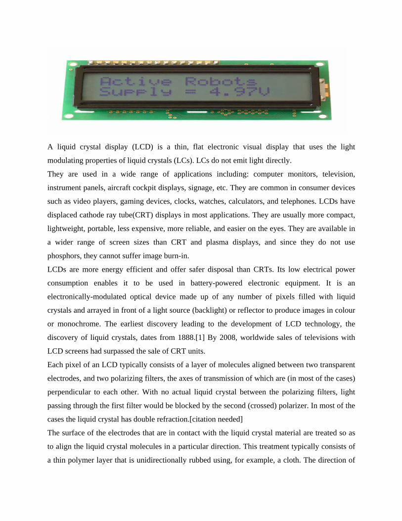
BUZZER:
A buzzer or beeper is an audio signaling device, which may be mechanical, electromechanical,
or electronic. Typical uses of buzzers and beepers include alarms, timers and confirmation of
user input such as a mouse click or keystroke.
A piezoelectric element may be driven by an oscillating electronic circuit or other audio signal
source. Sounds commonly used to indicate that a button has been pressed are a click, a ring or a
beep. Electronic buzzers find many applications in modern days.
RESET SWITCH:
It is used to reset the lcd display screen such that the new readings can be taken.
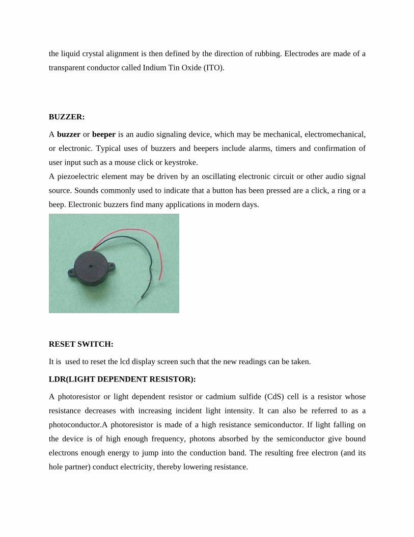
LDR(LIGHT DEPENDENT RESISTOR):
A photoresistor or light dependent resistor or cadmium sulfide (CdS) cell is a resistor whose
resistance decreases with increasing incident light intensity. It can also be referred to as a
photoconductor.A photoresistor is made of a high resistance semiconductor. If light falling on
the device is of high enough frequency, photons absorbed by the semiconductor give bound
electrons enough energy to jump into the conduction band. The resulting free electron (and its
hole partner) conduct electricity, thereby lowering resistance.
A photoelectric device can be either intrinsic or extrinsic. An intrinsic semiconductor has its own
charge carriers and is not an efficient semiconductor, e.g. silicon. In intrinsic devices the only
available electrons are in the valence band, and hence the photon must have enough energy to
excite the electron across the entire bandgap. Extrinsic devices have impurities, also called
dopants, added whose ground state energy is closer to the conduction band; since the electrons
do not have as far to jump, lower energy photons (i.e., longer wavelengths and lower
frequencies) are sufficient to trigger the device. If a sample of silicon has some of its atoms
replaced by phosphorus atoms (impurities), there will be extra electrons available for conduction.
This is an example of an extrinsic semiconductor.
Photoresistors come in many different types. Inexpensive cadmium sulfide cells can be found in
many consumer items such as camera light meters, street lights, clock radios, alarms, and
outdoor clocks.
They are also used in some dynamic compressors together with a small incandescent lamp or
light emitting diode to control gain reduction.
Lead sulfide (PbS) and indium antimonide (InSb) LDRs (light dependent resistor) are used for
the mid infrared spectral region. Ge:Cu photoconductors are among the best far-infrared
detectors available, and are used for infrared astronomy and infrared spectroscopy.
Transducers are used for changing energy types.
LED(LIGHT EMITTING DIODE):
A light-emitting diode (LED) (pronounced /��l i� �di�/[1]) is a semiconductor light source.
LEDs are used as indicator lamps in many devices, and are increasingly used for lighting.
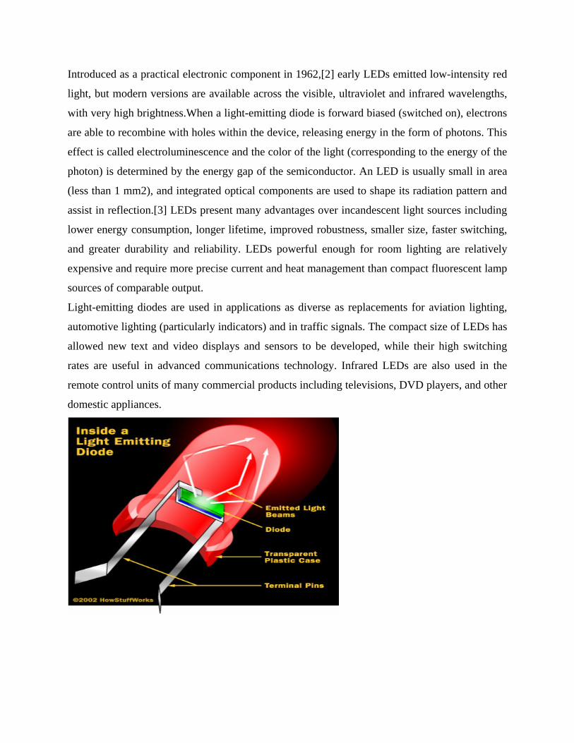
Introduced as a practical electronic component in 1962,[2] early LEDs emitted low-intensity red
light, but modern versions are available across the visible, ultraviolet and infrared wavelengths,
with very high brightness.When a light-emitting diode is forward biased (switched on), electrons
are able to recombine with holes within the device, releasing energy in the form of photons. This
effect is called electroluminescence and the color of the light (corresponding to the energy of the
photon) is determined by the energy gap of the semiconductor. An LED is usually small in area
(less than 1 mm2), and integrated optical components are used to shape its radiation pattern and
assist in reflection.[3] LEDs present many advantages over incandescent light sources including
lower energy consumption, longer lifetime, improved robustness, smaller size, faster switching,
and greater durability and reliability. LEDs powerful enough for room lighting are relatively
expensive and require more precise current and heat management than compact fluorescent lamp
sources of comparable output.
Light-emitting diodes are used in applications as diverse as replacements for aviation lighting,
automotive lighting (particularly indicators) and in traffic signals. The compact size of LEDs has
allowed new text and video displays and sensors to be developed, while their high switching
rates are useful in advanced communications technology. Infrared LEDs are also used in the
remote control units of many commercial products including televisions, DVD players, and other
domestic appliances.
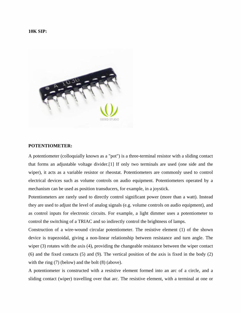
10K SIP:
POTENTIOMETER:
A potentiometer (colloquially known as a "pot") is a three-terminal resistor with a sliding contact
that forms an adjustable voltage divider.[1] If only two terminals are used (one side and the
wiper), it acts as a variable resistor or rheostat. Potentiometers are commonly used to control
electrical devices such as volume controls on audio equipment. Potentiometers operated by a
mechanism can be used as position transducers, for example, in a joystick.
Potentiometers are rarely used to directly control significant power (more than a watt). Instead
they are used to adjust the level of analog signals (e.g. volume controls on audio equipment), and
as control inputs for electronic circuits. For example, a light dimmer uses a potentiometer to
control the switching of a TRIAC and so indirectly control the brightness of lamps.
Construction of a wire-wound circular potentiometer. The resistive element (1) of the shown
device is trapezoidal, giving a non-linear relationship between resistance and turn angle. The
wiper (3) rotates with the axis (4), providing the changeable resistance between the wiper contact
(6) and the fixed contacts (5) and (9). The vertical position of the axis is fixed in the body (2)
with the ring (7) (below) and the bolt (8) (above).
A potentiometer is constructed with a resistive element formed into an arc of a circle, and a
sliding contact (wiper) travelling over that arc. The resistive element, with a terminal at one or
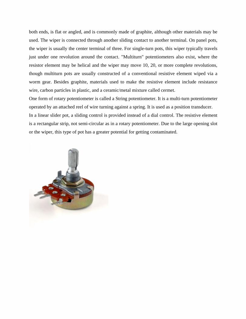
both ends, is flat or angled, and is commonly made of graphite, although other materials may be
used. The wiper is connected through another sliding contact to another terminal. On panel pots,
the wiper is usually the center terminal of three. For single-turn pots, this wiper typically travels
just under one revolution around the contact. "Multiturn" potentiometers also exist, where the
resistor element may be helical and the wiper may move 10, 20, or more complete revolutions,
though multiturn pots are usually constructed of a conventional resistive element wiped via a
worm gear. Besides graphite, materials used to make the resistive element include resistance
wire, carbon particles in plastic, and a ceramic/metal mixture called cermet.
One form of rotary potentiometer is called a String potentiometer. It is a multi-turn potentiometer
operated by an attached reel of wire turning against a spring. It is used as a position transducer.
In a linear slider pot, a sliding control is provided instead of a dial control. The resistive element
is a rectangular strip, not semi-circular as in a rotary potentiometer. Due to the large opening slot
or the wiper, this type of pot has a greater potential for getting contaminated.
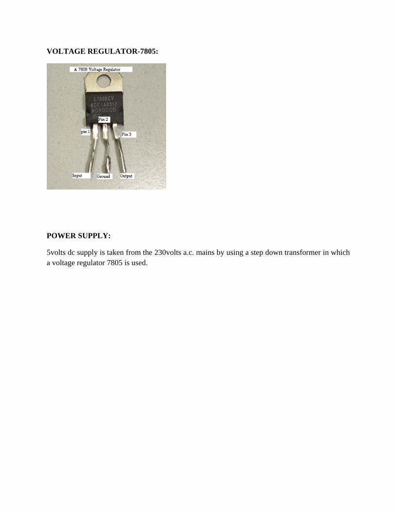
VOLTAGE REGULATOR-7805:
POWER SUPPLY:
5volts dc supply is taken from the 230volts a.c. mains by using a step down transformer in which a voltage regulator 7805 is used.
4.CIRCUIT EXPLANATION AND PROGRAMMING
The input we are using is a voltage of magnitude 5 volts.It consists of an AC
input of 230 V and a bridge circuit of diodes which acts as a rectifier.7805 is also used which is
connected to the bridge circuit inorder to get an output of 5 volts DC.
Firstly,on speaking about the temperature measuring unit,we are using LM35A as
the temperature sensor. And,the other part which measures the heart rate consists of an LED
which is connected to the input Vcc through a resistance of 330KOHM and an LDR with a
potentiometer.The function of an LED is it shows the property of electroluminiscence. When
LDR absorbs the light from the LED, its resistance varies inversely with respect to the intensity
of light it absorbs.Potentiometer does the work of finding the voltage magnitude. The input of
5volts is connected to a pin of LM35A(here 3A).The pin 2A is connected to the input(+IN) of an
ADC(Analog to Digital Converter).Here,the analog to digital converter we are using is
ADC0804.And the pin 3A is connected is grounded.
LM35A(temperature sensor), is exposed to certain temperature which acts as an input. LM35A
does the function of varying its output with respect to the change in the temperature that is given
as input.There by,the output voltage coresponds to the temperature that is sensed by LM35A.
Now,coming to ADC0804,each of the pins 1(CS),7(-IN),8(AGND) and
10(DGND) are grounded.The pin4(CLKIN) is connected to the pin1(CS) through 150pF
capacitor and the pin19(CLKR)
is connected to the pin4(CLKIN) THROUGH A 10KOHM resistance.These connections help in
the timing function of ADC0804.The pins 11,12,13,14,15,16,17,18 which are
DB7,DB6,DB5,DB4,DB3,DB2,DB1,DB0 respectively are connected to the resistance pins
2,3,4,5,6,7,8,9 respectively of 10K sip which inturn are connected to the pins
39(P0.7/AD7),38(P0.6/AD6),37(P0.5/AD5),36(P0.4/AD4),35(P0.3/AD3),34P0.2/AD2),33(P0.1/
AD1),32(P0.0/AD0) of the microcontroller AT89S52 respectively.
ADC0804 converts the input analog signal into an elactrical signal in which
is in the form of digital data.

Port 0 is an 8-bit open drain bidirectional I/O port. As an output port, each pin can sink eight
TTL inputs. The first pin of 10K sip is connected to the input voltage i.e., Vcc=5 volts.The 20th
pin (Vref/Vcc) of ADC0804 is also connected to the input voltage of magnitude 5 volts which is
needed for ADC0804 to work.The pins 2(RD),3(WR),5(INTR) are connected to the pins
10(P3.0),11(P3.1),12(P3.2) of the microcontroller 89S52 respectively.
The microcontroller AT89S52's Port 3 output buffers can sink/source four TTL inputs. When 1s
are written to Port 3 pins, they are pulled high by the inter-nal pull-ups and can be used as inputs.
As inputs, Port 3 pins that are externally being pulled low will source current (IIL) because of the
pull-ups. Port 3 receives some control signals for Flash programming and verification.The
connection between the pins 2,3,5 of ADC0804 and 10,11,12 of AT89S52 function based on the
program that is shown below
rd=1;
intr=1;
adcdata=0xff;
while(1)
{
lcdcmd(0xc2);
//delay(500);
wr=0;
_nop_();
_nop_();
_nop_();
_nop_();
wr=1;
delay(50);
rd=0;
delay(10);
a=adcdata;
convert(a);
delay(500);
The RST PIN of AT89S52 is connected to a capacitor of capacitance 10micro
farads and a reset switch(RESET SW) which are drawn fron the input Vcc i.e., 5 volts.Reset
input,a high on this pin for two machine cycles while the oscillator is running resets the device.
This pin drives high for 98 oscillator periods after the Watchdog times out. XTAL2 which is the
output from the inverting oscillator amplifier is connected to a 33pF capacitance which,inturn
connected to the pin9 through 8.2KOHM resistance and is grounded.XTAL1 which is the input
to the inverting oscillator amplifier and input to the internal clock operating circuit is connected
to XTAL1 with a capacitance of 33pF and parallelly the frequency of 11.0592MHz.The Vcc pin
and EA pinof AT89S52 are connected to the input of magnitude 5 volts which are inturn
connected to the pins 1 and 15 of LCD.EA enables the external access for AT89S52.
Port 1 is an 8-bit bidirectional I/O port with internal pull-ups. The Port 1 output
buffers can sink/source four TTL inputs. When 1s are written to Port 1 pins, they are pulled high
by the inter-nal pull-ups and can be used as inputs. As inputs, Port 1 pins that are externally
being pulled low will source current (IIL) because of the internal pull-ups. The pins 6,7,8 help in
system programming. The pins 9,8,7,6,5,4,3 of AT89S52 are connected to 4,6,11,12,13,14 pins
of LCD respectively.
The pin 15 is connected to a buzzer through a resistance of 1kohm and a transistor BC547 and is
grounded.Buzzer is a piezo electric material which converts the sound activity(here,the heart beat
rythm) into an electric signal.Buzzer is also given the input Vcc ie.,5volts (DC) and the same
input is also given to the base of the transistor BC547.The emitter of the transistor is
grounded.The pin 2 of LCD is grounded.And the pins 1,5 and 16 are grounded.The pin 2 is
grounded through a resistance that is connected to rheostat that connects to pin3 which is also
grounded.The function of buzzer and its dependance on LCD for the display of values of
heartbeat count is carried out using the following program instructions:

void main() { buz=0; finger=1; lcd_init(); lcdcmd(0x85); msgdisplay("WELCOME"); lcdcmd(0x01); msgdisplay("temp hbeat"); rd=1; intr=1; adcdata=0xff; while(1) { lcdcmd(0xc2); //delay(500); wr=0; _nop_(); _nop_(); _nop_(); _nop_(); wr=1; delay(50); rd=0; delay(10); a=adcdata; convert(a); delay(500); for(i=0;i<100;i++) { count+=1; if(finger==0) { delay(1000); if(!finger) { buz=1; delay(500); pp=1; buz=0; break; } else pp=0; } }

delay(500); lcdcmd(0xca); if(pp) { convert(count); } else convert(0); pp=0; } } The above program asserts the input data.If the sensor senses the subject’s finger,then the input of the buzzer is set to higher logic state otherwise the input of the buzzer is set to 0. And finally the lcd also shows the temperature readings based on the following program instructions:
void convert(unsigned char temp_value) { unsigned char value,d1,d2,d3; temp_value = temp_value; value=temp_value/10; d3=temp_value%10; d1=value/10; d2=value%10; d1=d1+0x30; lcddata(d1); delay(10); d2=d2+0x30;

5.MICROCONTROLLER PROGRAMMING:
#include<reg51.h> #include"lcddisplay.h" #include<intrins.h> sbit rd = P2^0; sbit wr = P2^1; sbit intr = P2^2; sbit finger = P2^5; sbit buz = P2^3; #define adcdata P3 void convert(unsigned char ); unsigned char a,pp=0,count=0,i; void main() { buz=0; finger=1; lcd_init(); lcdcmd(0x85); msgdisplay("WELCOME"); lcdcmd(0x01); msgdisplay("temp hbeat"); rd=1; intr=1; adcdata=0xff; while(1) { lcdcmd(0xc2); //delay(500); wr=0; _nop_(); _nop_(); _nop_(); _nop_(); wr=1;

delay(50); rd=0; delay(10); a=adcdata; convert(a); delay(500); for(i=0;i<100;i++) { count+=1; if(finger==0) { delay(1000); if(!finger) { buz=1; delay(500); pp=1; buz=0; break; } else pp=0; } } delay(500); lcdcmd(0xca); if(pp) { convert(count); } else convert(0); pp=0; } } void convert(unsigned char temp_value) { unsigned char value,d1,d2,d3;
temp_value = temp_value; value=temp_value/10; d3=temp_value%10; d1=value/10; d2=value%10; d1=d1+0x30; lcddata(d1); delay(10); d2=d2+0x30; lcddata(d2); delay(4); // msgdisplay("."); d3=d3+0x30; lcddata(d3); delay(10); }

6.APPLICATIONS:
The instrument consists of the circuits which measure both the heart rate and temperature has various applications.
1.Heart rate monitor can be used in hospitals for the diagnostic purposes.
2.Since the instrument is not expensive,it can even be used at home.
3.The instrument also has the flexibility which helps us to affix it to vehicles,etc..
4.The other part of the instrument,which measures the temperature can also be used in hospitals for diagnostic purpose.
5.The instrument can also be integrated with higher level equipment and used in various applications.
6.The instrument can also be used in watches,etc.

7.CONCLUSION:
Hence the attempt made by us in designing an instrument which can measure both temperature and heart rate is successful.


