Embed Size (px)
Citation preview

Influence of High-G Mechanical Shock and Thermal Cyclingon Localized Recrystallization in Sn-Ag-Cu Solder Interconnects
TAE-KYU LEE,1,4 CHOONG-UN KIM,2 and THOMAS R. BIELER3
1.—Component Quality and Technology Group, Cisco Systems, Inc., San Jose, CA 95134, USA.2.—University of Texas, Arlington, TX, USA. 3.—Michigan State University, East Lansing, MI,USA. 4.—e-mail: [email protected]
The impact of isothermal aging and recrystallized grain structure distributionon mechanical shock and thermal cycling performance of solder joints with 1%and 3% silver content Sn-Ag-Cu interconnects were investigated. Localizedrecrystallized grain structure distributions were analyzed to identify corre-lations between the microstructure evolution and shock performance. Theresults reveal that the shock tolerance depends on the amount of shock energythat can be absorbed during each shock cycle, which depends on microstruc-tural features. Based on the recrystallized grain distribution, additional iso-thermal aging in 1% silver Sn-Ag-Cu interconnects shows improved shockperformance, whereas degraded shock performance was observed in 3%Sn-Ag-Cu interconnects. Using the same grain boundary distribution analysison thermally cycled samples, relationships between the particle size distri-bution, localized recrystallized grain structure development, shock, andthermomechanical performance were identified: finer particle spacing is ben-eficial for thermal cycling as it resists grain boundary generation, while con-versely, wider particle spacing facilitates recrystallization and grain boundarymobility that allows Sn to absorb shock energy.
Key words: Mechanical shock, thermal cycling, solder, isothermal aging,recrystallization
INTRODUCTION
The mechanical and thermal stability of solderinterconnects under dynamic shock and thermalcycling conditions are crucial for high-reliabilityelectronic devices.1–5 To have a stable interconnectin a mechanical shock environment, the intercon-nections need to tolerate mechanical strain, whichdevelops in a way that is dependent upon the reac-tion between the component location and appliedshock.6–9 Given that failure locations vary from thepackage-side interface intermetallics to the lami-nate area immediately below the Cu pad or trace,mitigation or delay of crack initiation can beaccomplished if the mechanisms of shock energyabsorption in the interconnection system can be
identified.10,11 For example, a recent study onmicroalloyed solder interconnects showed improvedshock performance by absorbing the shock energyand strain induced by the shock through generationof mechanical twins.12 Thus, mechanical twinningmay be a potential mitigation mechanism toimprove performance if alloying or microstructuredesign can facilitate mechanical twinning. Otherthan adding a microalloying element, it has alreadybeen demonstrated that lower-silver-content alloyoffers better mechanical shock performance thanhigher-silver-content Sn-Ag-Cu solder.13,14 Less Agcontent resulted in less Ag3Sn intermetallic com-pound (IMC) precipitates and thus softer bulk sol-der compared with higher-Ag solder alloys, whichconveys less shock-induced strain at the interfacialstress concentration locations, resulting in bettershock performance. With thermal aging, the IMCparticles coarsen into larger, fewer, and more(Received April 26, 2013; accepted August 14, 2013;
published online September 4, 2013)
Journal of ELECTRONIC MATERIALS, Vol. 43, No. 1, 2014
DOI: 10.1007/s11664-013-2736-3� 2013 TMS
69

widely spaced IMCs in the microstructure,13–15
which also provides a softer and more shock-tolerant microstructure. However, while this soft-ening effect is important for shock performance,higher Ag content in Sn-Ag-Cu interconnects isadvantageous for slowing thermal-cycling-inducedfatigue damage.15 Thus, there is a tradeoff betweenstrength, ductility, and the effects of the details ofrecrystallization and damage nucleation processesthat needs to be examined. So far, comparison be-tween such low- and high-Ag-content solder alloyshas focused on the role of Ag3Sn IMC precipitates.But recently, the transformation from single- tomultigrain recrystallized grain structure and itsrelationship with thermomechanical performancehave been studied.16–21
In this study, SAC105 solder alloy was comparedwith SAC305 solder alloy to assess the effect of iso-thermal aging and recrystallization on high-G board-level shock performance and thermal cycling lifetimetests. By following the evolution of the grain struc-ture and distribution, interrelationships between thegrain size distribution, mechanical shock, and ther-mal cycling performance are identified.
EXPERIMENTAL PROCEDURES
As shown in Fig. 1a, the samples used in this studywere 12 mm 9 12 mm body size ball grid arrays(BGAs) with a three-row perimeter array and a totalof 228 solder joints. The solder ball diameter was350 lm, and they were arranged in the package witha 0.5 mm pitch. The composition of the solder ballsused in this study was Sn-1.0Ag-0.5Cu (wt.%)(SAC105) or Sn-3.0Ag-0.5Cu (wt.%) (SAC305). All
BGA samples had a 10.05 mm 9 10.05 mm silicondie attached, and the package-side substrates hadelectrolytic Ni/Au surface finish on top of the Cu pads.The packages were assembled onto 1.65 mm (62 mil)high-Tg FR4 boards for shock testing and 2.36 mm(93 mil) boards for thermal cycling, which had anorganic surface preservative surface finish. Thereflow condition was 1 min above the liquidus with a245�C peak temperature profile.
A top view of the test board used in this study forboth thermal cycling and shock tests is shown inFig. 1b, where there are nine components per board.For a given input shock event, each location experi-enced a different shock level and strain level. The testvehicle was designed to provide three different shockand strain conditions, and the shock and strainresponse is explained in detail in earlier publica-tions.12,22 A fixed input shock of 1500G with 0.5-mshalf-sine pulse duration at the table was imposed,which is based on the JEDEC22-B111 standard.23 Ahigh-acceleration shock tester (KD, DP-1200-18model) was used for measuring the shock level, and athree-axis strain gauge with 1 mm gauge length wasused for strain measurements. The connectionsbetween the component daisy-chains were monitoredcontinuously, and a 20% increase in resistance dur-ing the shock test, compared with the initial resis-tivity value, was considered to be a failure.
The measured maximum principal strain andmaximum shock level for different locations on theboard with a 1500G table shock input are shown inFig. 2. Center, edge, and corner location shock andstrain were measured by strain gauges and acceler-ometers A, B, and C, as indicated in Fig. 3b. A higherstrain value is detected at the edge location for a given
Fig. 1. Sample component (a) and shock test board (b) schematics. Locations of packages U1 to U9, strain gauges, and accelerometers areindicated on the board.
Lee, Kim, and Bieler70

shock level compared with center or corner locations,as shown in the plot. Lower shock/lower strainoccurred at the corner locations (U1, U7, U3, and U9),and at the edge locations (U2, U4, U6, and U8), alower shock/higher strain condition occurred.
Accelerated thermal cycling (ATC) was conductedon samples using a 0�C to 100�C thermal cycle witha ramp rate of 10�C/min and 10 min of dwell time.Continuous resistivity measurement was appliedfor in situ monitoring during the test. The failurecriterion used for the study was a consistent 20%increase in the peak resistivity from the initialvalue for 5 sequential cycles. Eighteen data points
per precondition were collected and plotted usingWeibull statistics.
To study the effect of isothermal aging, some sam-ples used for both thermal cycling and shock testswere isothermally aged at 150�C for 500 h in ambientair, and the mechanical and thermal performancewith and without isothermal aging were assessed. Toidentify the crack locations and their distribution inthe sample, cross-section and dye-and-pry methodswere used; details can be found in an earlier publi-cation.24 To observe the microstructure while mini-mizing sample preparation artifacts, the sampleswere cut with an abrasive cutter to a size that per-mitted mounting in epoxy, sufficiently away from theedge solder joints, then ground and polished with 600grit SiC paper to a location near the center of thesolder joint, followed by higher-grit papers. For finalpolishing, a polishing cloth with ultrafine colloidalsilica suspension (<0.04 lm) was used. Both bright-field and polarized optical and SEM were used toidentify the crack propagation path. Polarized-lightimages were used to identify initial and recrystallizedgrain structures.
RESULTS AND DISCUSSION
The SEM cross-section microstructures of theinitial state at the package-side and board-sideinterfaces are shown in Fig. 3, which compares themicrostructure of SAC105 and SAC305 before andafter isothermal aging. The package-side interfaceshowed a needle-shaped IMC layer which is(Cu,Ni)6Sn5 with a fine distribution of Ag3Sn insidethe solder bulk area near the interface, which can be
0
500
1000
1500
2000
2500
3000
Component Location
Max
imu
m m
easu
red
sh
ock
leve
l (G
)
Corner Edge Center
Measured shock level (G)
Table shock input
500
750
1000
1250
1500
1750
2000
2250
2500
Maxim
um
Micro
strain
Max principle + strain Max principle - strain average
Fig. 2. Measured shock level and microstrain with 1500G tableshock input. Center, edge, and corner location shock and strainmeasured by strain gauge and accelerometer A, B, and C, respec-tively, as indicated in Fig. 1b.
(a) (b) (c) (d)
(e) (f) (g) (h)
Fig. 3. Scanning electron microscopy cross-section microstructure of SAC105 (a, e) before aging and (b, f) after aging at 150�C/500 h, andSAC305 (c, g) before aging and (d, h) after aging at 150�C/500 h.
Influence of High-G Mechanical Shock and Thermal Cycling on Localized Recrystallizationin Sn-Ag-Cu Solder Interconnects
71
seen in other publications.13–15 Compared withSAC105, SAC305 shows finer and more abundantAg3Sn precipitates in the solder b-Sn matrix. Afterisothermal aging, coalescence of IMC precipitatesand thickening of the IMC layer at the interfacewere observed. Both SAC105 and SAC305 showedless in number and larger in size IMC precipitatesafter isothermal aging. Near the board-side inter-face, the Cu diffused further into the bulk andformed additional Cu6Sn5 precipitates.
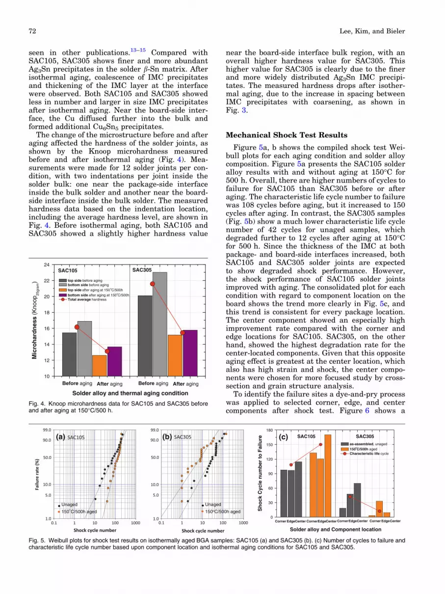
The change of the microstructure before and afteraging affected the hardness of the solder joints, asshown by the Knoop microhardness measuredbefore and after isothermal aging (Fig. 4). Mea-surements were made for 12 solder joints per con-dition, with two indentations per joint inside thesolder bulk: one near the package-side interfaceinside the bulk solder and another near the board-side interface inside the bulk solder. The measuredhardness data based on the indentation location,including the average hardness level, are shown inFig. 4. Before isothermal aging, both SAC105 andSAC305 showed a slightly higher hardness value
near the board-side interface bulk region, with anoverall higher hardness value for SAC305. Thishigher value for SAC305 is clearly due to the finerand more widely distributed Ag3Sn IMC precipi-tates. The measured hardness drops after isother-mal aging, due to the increase in spacing betweenIMC precipitates with coarsening, as shown inFig. 3.
Mechanical Shock Test Results
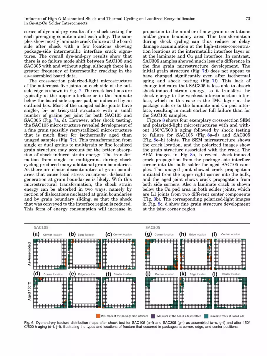
Figure 5a, b shows the compiled shock test Wei-bull plots for each aging condition and solder alloycomposition. Figure 5a presents the SAC105 solderalloy results with and without aging at 150�C for500 h. Overall, there are higher numbers of cycles tofailure for SAC105 than SAC305 before or afteraging. The characteristic life cycle number to failurewas 108 cycles before aging, but it increased to 150cycles after aging. In contrast, the SAC305 samples(Fig. 5b) show a much lower characteristic life cyclenumber of 42 cycles for unaged samples, whichdegraded further to 12 cycles after aging at 150�Cfor 500 h. Since the thickness of the IMC at bothpackage- and board-side interfaces increased, bothSAC105 and SAC305 solder joints are expectedto show degraded shock performance. However,the shock performance of SAC105 solder jointsimproved with aging. The consolidated plot for eachcondition with regard to component location on theboard shows the trend more clearly in Fig. 5c, andthis trend is consistent for every package location.The center component showed an especially highimprovement rate compared with the corner andedge locations for SAC105. SAC305, on the otherhand, showed the highest degradation rate for thecenter-located components. Given that this oppositeaging effect is greatest at the center location, whichalso has high strain and shock, the center compo-nents were chosen for more focused study by cross-section and grain structure analysis.
To identify the failure sites a dye-and-pry processwas applied to selected corner, edge, and centercomponents after shock test. Figure 6 shows a
10
12
14
16
18
20
22
24
After aging
Solder alloy and thermal aging condition
SAC305
Mic
roh
ard
nes
s (K
noop
25gr
am) top side before aging
bottom side before agingtop side after aging at 150oC/500hbottom side after aging at 150oC/500hTotal average hardness
SAC105
Before aging After agingBefore aging
Fig. 4. Knoop microhardness data for SAC105 and SAC305 beforeand after aging at 150�C/500 h.
0
30
60
90
120
150
180
SAC105
Sh
ock
Cyc
le n
um
ber
to
Fai
lure
Solder alloy and Component location
CenterEdgeCorner
as-assembled, unaged150oC/500h agedCharacteristic life cycle
CenterEdgeCorner CenterEdge CenterCorner EdgeCorner
SAC305
Unaged
150°C/500h aged
Unaged
150oC/500h aged
(a) (b) (c)
Fig. 5. Weibull plots for shock test results on isothermally aged BGA samples: SAC105 (a) and SAC305 (b). (c) Number of cycles to failure andcharacteristic life cycle number based upon component location and isothermal aging conditions for SAC105 and SAC305.
Lee, Kim, and Bieler72
series of dye-and-pry results after shock testing foreach pre-aging condition and each alloy. The sam-ples show mostly laminate crack failure at the boardside after shock with a few locations showingpackage-side intermetallic interface crack signa-tures. The overall dye-and-pry results show thatthere is no failure mode shift between SAC105 andSAC305 with and without aging, although there is agreater frequency of intermetallic cracking in theas-assembled board data.
The cross-section polarized-light microstructureof the outermost five joints on each side of the out-side edge is shown in Fig. 7. The crack locations aretypically at the upper interface or in the laminatebelow the board-side copper pad, as indicated by anoutlined box. Most of the unaged solder joints havesingle-, bi- or tricrystal structure with a smallnumber of grains per joint for both SAC105 andSAC305 (Fig. 7a, d). However, after shock testing,the SAC105 microstructure revealed development ofa fine grain (possibly recrystallized) microstructurethat is much finer for isothermally aged thanunaged samples (Fig. 7c). This transformation fromsingle or dual grains to multigrain or fine localizedgrain structure may account for the better absorp-tion of shock-induced strain energy. The transfor-mation from single to multigrains during shockcycling produced many additional grain boundaries.As there are elastic discontinuities at grain bound-aries that cause local stress variations, dislocationgeneration at grain boundaries is likely. With thismicrostructural transformation, the shock strainenergy can be absorbed in two ways, namely bymotion of dislocations nucleated at grain boundariesand by grain boundary sliding, so that the shockthat was conveyed to the interface region is reduced.This form of energy consumption will increase in
proportion to the number of new grain orientationsand/or grain boundary area. This transformationduring shock cycling can thus reduce or delaydamage accumulation at the high-stress-concentra-tion locations at the intermetallic interface layer orat the laminate and Cu pad interface. In contrast,SAC305 samples showed much less of a difference inthe fine grain microstructure development. Theinitial grain structure (Fig. 7d) does not appear tohave changed significantly even after isothermalaging and shock testing (Fig. 7f). This lack ofchange indicates that SAC305 is less able to absorbshock-induced strain energy, so it transfers theshock energy to the weakest interconnection inter-face, which in this case is the IMC layer at thepackage side or to the laminate and Cu pad inter-face, resulting in much earlier full failure than forthe SAC105 samples.
Figure 8 shows four exemplary cross-section SEMand polarized-light microstructures with and with-out 150�C/500 h aging followed by shock testingto failure for SAC105 (Fig. 8a–d) and SAC305(Fig. 8e–h) joints. The SEM microstructure showsthe crack location, and the polarized images showthe grain structure associated with the crack. TheSEM images in Fig. 8a, b reveal shock-inducedcrack propagation from the package-side interfacecorner into the bulk solder for aged SAC105 sam-ples. The unaged joint showed crack propagationinitiated from the upper right corner into the bulk,and the aged joint shows crack propagation fromboth side corners. Also a laminate crack is shownbelow the Cu pad area in both solder joints, whichare L1 joints from two different center components(Fig. 3b). The corresponding polarized-light imagesin Fig. 8c, d show fine grain structure developmentat the joint corner region.
Corner location Edge location Center location Corner location Edge location Center location(a) (b) (c) (g) (h) (i)
Corner location Edge location Center location Corner location Edge location Center location(d) (e) (f) (j) (k) (l)
Ag
ed 1
50°C
A
s-A
ssem
ble
d
Fig. 6. Dye-and-pry fracture distribution maps after shock test for SAC105 (a–f) and SAC305 (g–l) as assembled (a–c, g–i) and after 150�C/500 h aging (d–f, j–l), illustrating the types and locations of fracture that occurred in packages at corner, edge, and center positions.
Influence of High-G Mechanical Shock and Thermal Cycling on Localized Recrystallizationin Sn-Ag-Cu Solder Interconnects
73

Given the initial mostly single- or tricrystal grainstructure, the fine grain structure must havedeveloped during the shock test cycles. In contrastto SAC105, the crack propagated into the laminateregion as shown in Fig. 8e, f and there are very fewfine grains in the SAC305 joints in Fig. 8g, h. Thiscontrast suggests that the fine grain structure pro-vides many more energy-absorbing sites with theincrease in the number of grain boundaries. Thecompliance and easier deformation of SAC105 bulksolder in the interconnects led to the betterabsorption of shock-induced strain energy, which inturn resulted in multigrain or finer grain micro-structure development, possibly through bothdynamic and static recrystallization during andfollowing each shock event. Without the fine grainstructure development in SAC305, deformation ofthe bulk solder was difficult and little shock-inducedstrain was absorbed, which ultimately transferredthe stress and strain directly to the IMC and the Cutrace laminate interfaces, resulting in earlier crackinitiation and propagation compared with the moreshock-absorbing SAC105. In addition to the effect ofthe alloy composition and precipitate microstruc-ture, isothermal aging increased the shock absorp-tion capability and actually improved the shockperformance in SAC105. After isothermal aging in
the SAC105 joints, the bulk solder became softer,which further promoted bulk solder deformationand increased absorption of the shock-inducedstrain energy. Due to the increased strain energyabsorbed, microstructure features such as IMCprecipitate coarsening and consequently wider par-ticle spacing occurred, which favored dislocationaccumulation that enabled recrystallization. Withmore dynamic and static recrystallization, finergrain microstructures developed as shown inFigs. 7c and 8d.
Thermal Cycling Test Results
The thermal cycling performance for each con-dition is shown in Fig. 9, which shows the Weibullstatistics for SAC105 and SAC305 with and with-out aging. For both alloys, the thermal cyclingcharacteristic life cycle number degraded afteraging to nearly the same value, but the number ofcycles before failure for the unaged SAC305 wasmuch higher. As reported in other publications,isothermal aging facilitates microstructural evolu-tion by recrystallization mechanisms in the inter-face region, and formation of random high-angleboundaries facilitates crack nucleation andgrowth.25,26
L1 L2 L3 L4 L5 R5 R4 R3 R2 R1
L1 L2 L3 L4 L5 R5 R4 R3 R2 R1
L1 L2 L3 L4 L5 R5 R4 R3 R2 R1
(a)
(b)
(c)
L1 L2 L3 L4 L5 R5 R4 R3 R2 R1
L1 L2 L3 L4 L5 R5 R4 R3 R2 R1
L1 L2 L3 L4 L5 R5 R4 R3 R2 R1
(d)
(e)
(f)
SAC105
SAC305
Initial state, As Fabricated
After cyclic shock, no isothermal aging pre-condition
After cyclic shock, with isothermal aging pre-condition
Left side corner Right side corner
Initial state, As Fabricated
After cyclic shock, no isothermal aging pre-condition
After cyclic shock, with isothermal aging pre-condition
Left side corner Right side corner
Fig. 7. Polarized-light microstructure cross-sections of the 10 joints marked in Fig. 1 before and after shock testing for (a–c) SAC105 and (d–f)SAC305: as assembled (a, d), after shock test (b, e), and after 150�C/500 h aging and shock test (c, f). The crack locations are indicated byboxes.
Lee, Kim, and Bieler74

In the polarized-light microstructures of thethermally cycled samples in Fig. 10, overlaid boxesshow the locations of cracks that developed near thepackage-side interface. Due to the effect of the diesize, most of the damage occurred at the corner-most joint, which shows full crack propagation ineach condition. In SAC105, a wide range of full andpartial cracks were observed (indicated in boxes),whereas more localized cracks, limited to the cor-ner-most joints, were developed in SAC305 samples.
Comparison Between Shock and ThermalCycling Microstructural Evolution
To quantify the grain structure evolution, a sim-ple method was used to identify the number of grainboundaries per joint in the region close to theinterface. Based on ASTM-E112,27 the number ofgrain boundaries through which a line passed, wascounted near the package-side interface and the
board-side interface, as illustrated in Fig. 11. Thecumulative number of boundaries for all 10 joints(identified in Fig. 3a) per condition along the upper(lower) line of each joint is marked with an up(down) pointing triangle, and plotted with jointposition in Fig. 12. In each plot, effects of shock(blue, purple) or thermal cycling (red, orange) areshown with respect to the distribution prior to shockor thermal cycling (black, gray).
By comparing the grain boundary number distri-bution in SAC105 and SAC305 nonaged and agedconditions, the effects of thermal cycling and shockon the overall grain structure development can beobserved. Figure 12a, e and c, g show the grainboundary distribution after shock testing forSAC105 and SAC305 for the unaged (a, c) and aged(e, g) conditions. For the unaged samples, the grainstructure development after shock test did not showmuch change for either SAC105 or SAC305 joints.On the other hand, aging resulted in an increase in
1000
1250
1500
1750
2000
2250
2500
2750
3000
SAC305
Th
erm
al li
fe c
ycle
nu
mb
er t
o F
ailu
re
Alloy and pre-condition
as-assembled, no aging 150oC/500h aged First failure cycle number
As-assembled, no aging
After aging
150oC/500h
As-assembled, no aging
After aging150oC/500h
SAC105(c)
Fig. 9. Weibull plots for thermal cycling test results on the isothermally aged BGA samples of SAC105 (a) and SAC305 (b). (c) Characteristic lifecycle number to failure and first failure cycle based upon solder alloy and isothermal aging conditions for SAC105 and SAC305.
(a) (e)(b) (f)
(c) (g)(d) (h)
Fig. 8. Selected cross-section SEM and associated polarized image microstructure before (a, c, e, g) and after 150�C/500 h aging (b, d, f, h)followed by shock testing to failure for SAC105 (a–d) and SAC305 (e–h). The SEM microstructure shows the crack location in the joint andlaminate [white arrows (a, b, e, f)], and the polarized images show the grain structure associated with the characteristic life cycles to failureindicated (c, d, g, h).
Influence of High-G Mechanical Shock and Thermal Cycling on Localized Recrystallizationin Sn-Ag-Cu Solder Interconnects
75

the number of grain boundaries, but the rate ofgrain boundary development was significantlyhigher in the SAC105 sample, which is correlatedwith the better shock performance.
The effect of thermal cycling can be compared inthe same way for the unaged (b, d) and aged (f, h)conditions. Without isothermal aging, a greaterincrease in grain boundary number was observed inSAC105 than SAC305. The five SAC105 cornerjoints from each side show a fairly uniform increasein the number of grain boundaries with position inthe joint. In contrast, only the corner-most SAC305solder joints show an increase in grain boundaries.Because SAC105 is more easily deformed than
SAC305, SAC105 joints show more widely distrib-uted multigrain structure development, and thismultigrain structure only develops in the mosthighly stressed SAC305 corner joints. The effect ofstress concentration is also evident in Fig. 12b,where the higher rate of grain boundary increase atthe package-side interface is related to the smallercross-sectional load-carrying area than the packageside. After isothermal aging, thermally cycledSAC105 joints also showed an increase in thenumber of grain boundaries, but at a significantlylower rate than the nonaged and thermally cycledsolder joints. The initially softer bulk structure ofaged SAC105 can account for this, because after
L1 L2 L3 L4 L5 R5 R4 R3 R2 R1
L1 L2 L3 L4 L5 R5 R4 R3 R2 R1
L1 L2 L3 L4 L5 R5 R4 R3 R2 R1
L1 L2 L3 L4 L5 R5 R4 R3 R2 R1
(a)
(b)
(c)
(d)
SAC105
SAC305
After Thermal cycling, no isothermal aging pre-condition
After Thermal cycling, with isothermal aging pre-condition
Left side corner Right side corner
After Thermal cycling, no isothermal aging pre-condition
After Thermal cycling, with isothermal aging pre-condition
Left side corner Right side corner
Fig. 10. Cross-section optical polarized image microstructure after thermal cycling to failure for SAC105 (a, b) and SAC305 (c, d): thermallycycled with no isothermal aging (a, c) and after 150�C/500 h aging and thermal cycling (b, d). Cross-section joint locations are indicated in Fig. 1.Observed crack locations are indicated in a box.
Fig. 11. Example of how the grain boundary number was counted in solder joints. Line P was drawn 50 lm from the package-side interface, andline B was drawn 50 lm from the board-side interface.
Lee, Kim, and Bieler76

isothermal aging, the bulk structure had a smallernumber of, but larger, IMC precipitates. More widelyspaced precipitates provide fewer pinning sites forgrain boundaries, so recrystallized grains are larger,
as predicted by the Zener limit [dmax = (2r)/(3Vf),where the maximum diameter d varies with particleradius r, for a given particle volume fraction Vf]. Onthe other hand, the SAC305 solder joints show a
0
4
8
12
16
20
To
tal G
rain
Bo
un
dar
y N
um
ber
Package side, as-assembledBoard side, as-assembledPackage side, after ShockBoard side, after Shock
Solder joint location
0
4
8
12
16
20Package side, as-assembledBoard side, as-assembledPackage side, after Thermal cyclingBoard side, after Thermal cycling
Solder joint location
L1 L2 L3 L4 L5 R5 R4 R3 R2 R1 L1 L2 L3 L4 L5 R5 R4 R3 R2 R1
0
4
8
12
16
20Package side, as-assembledBoard side, as-assembledPackage side, after Thermal cyclingBoard side, after Thermal cycling
0
4
8
12
16
20
To
tal G
rain
Bo
un
dar
y N
um
ber
Package side, as-assembledBoard side, as-assembledPackage side, after ShockBoard side, after Shock
L1 L2 L3 L4 L5 R5 R4 R3 R2 R1L1 L2 L3 L4 L5 R5 R4 R3 R2 R1
0
4
8
12
16
20Package side, 150oC/500h agedBoard side, 150oC/500h agedPackage side, aged + ShockBoard side, aged + Shock
To
tal G
rain
Bo
un
dar
y N
um
ber
0
4
8
12
16
20
L1 L2 L3 L4 L5 R5 R4 R3 R2 R1 L1 L2 L3 L4 L5 R5 R4 R3 R2 R1
Package side, 150oC/500h agedBoard side, 150oC/500h agedPackage side, aged + Thermal cyclingBoard side, aged + Thermal cycling
0
4
8
12
16
20Package side, 150oC/500h agedBoard side, 150oC/500h agedPackage side, aged + Thermal cyclingBoard side, aged + Thermal cycling
Solder joint location
0
4
8
12
16
20
To
tal G
rain
Bo
un
dar
y N
um
ber
L1 L2 L3 L4 L5 R5 R4 R3 R2 R1L1 L2 L3 L4 L5 R5 R4 R3 R2 R1
Package side, 150oC/500h agedBoard side, 150oC/500h agedPackage side, aged + ShockBoard side, aged + Shock
Solder joint location
(a) as-assembled, Shock tested
SA
C10
5S
AC
305
(c) as-assembled, Shock tested
(b) as-assembled, Thermal cycled
(d) as-assembled, Thermal cycled
(e) 150oC/500h aged, Shock tested
(g) 150oC/500h aged, Shock tested
(f) 150oC/500h aged, Thermal cycled
(h) 150oC/500h aged, Thermal cycled
SA
C10
5S
AC
305
Fig. 12. Grain number distribution based on solder joint location before and after thermal cycling and shock test for SAC105 (a, b, e, f) andSAC305 (c, d, g, h): before and after aging and shock test (a, c, e, g) and thermal cycling (b, d, f, h), for five joints from the left (L1 to L5) and right(R1 to R5) corner, as indicated in Fig. 3 (Color figure online).
Influence of High-G Mechanical Shock and Thermal Cycling on Localized Recrystallizationin Sn-Ag-Cu Solder Interconnects
77

greater increase of grain boundaries after aging inFig. 10h than without aging in Fig. 10d, and theenhancement at the corner joints is minimal. Thesedata are consistent with prior work that indicatesthat recrystallized grain structure development inaged samples is more active than in nonaged sam-ples, as reported earlier.16
The sums of these outcomes in Fig. 13 show thatgeneration of fine grains differs for every conditiontested. There is an overall trend for a greater amountof grain boundary development on the package sidethan the board side, which reflects the greater stresspresent on this side due to the smaller cross-sectionalarea. Higher stress would generate more strainenergy that provides a driving force for grainboundary motion via primary recrystallizationmechanisms. Also, with the exception of agedSAC105, there is more generation of boundariesarising from thermal cycling than shock deformation,which indicates the significance of the strain energyhysteresis loop arising from deformation where holdtimes increase the energy dissipated per cycle due tocreep/stress relaxation at differing temperatures.
In contrast, isothermal mechanical shock strainat a high strain rate does not lead to as much energystorage in the solder microstructure, due to the factthat Sn is stronger at high strain rate.28,29 Thisstrength is further increased in nonaged samples bya smaller particle spacing, and this leads to strainenergy transfer into the board that causes laminatecracking at the board side (hence the low number ofcycles to shock failure in SAC305). Only the agedSAC105 has few enough particles in an overagedcondition to make Sn easily deformable in shockconditions, as indicated by the greatest total num-ber of grain boundaries arising from shock condi-tions. This deformation then adds strain energy tothe Sn that facilitates generation of grain bound-aries by recrystallization processes that are ener-gized by the elastic strain energy dissipation during
and following the initial impact. This importantobservation is also supported by the lowest numberof shock cycles for aged SAC305, where apparentlythere was insufficient coarsening to soften the alloy,and too many particles to pin grain boundaries, sothat little boundary creation could develop.
Aging leads to similar thermal cycling toughnessin both alloys, indicating that a low number of, oroveraged, particles have a similar effect on grainboundary generation, and correspondingly a similarnumber of cycles to failure. However, the unagedSAC305 had the highest thermal cycling lifetime,correlated with the least number of boundariesgenerated, which is probably due to the finer pre-cipitate size that more effectively pinned subboun-daries and grain boundaries. This is consistent withthe similar number of thermal cycles to failure inSAC105 and SAC305 when there is a similarly largeparticle spacing. This analysis indicates that thereare different optimal particle spacing conditions fordifferent kinds of toughness requirements, whichcan be anticipated.
CONCLUSIONS
The effects of isothermal aging and recrystallizedgrain boundary distribution on mechanical shockand thermal cycling performance of solder jointswith 1% and 3% silver content in Sn-Ag-Cu inter-connects in unaged and aged microstructures wereinvestigated. The results revealed that joint stabil-ity for shock performance is sensitive to the pre-cipitate particle size and spacing, and this affectsrecrystallization processes leading to generation ofgrain boundaries. The localized recrystallized grainstructure was analyzed to identify correlationsbetween the microstructure evolution and shockperformance. This investigation examined the ori-gin of the better compliance of SAC105 solder inshock testing conditions. Two microstructural
0
20
40
60
80
100
120150oC/500h aged
ShockATCInitial
Not Aged
as-assembled package sideas-assembled board sidethermal cycled package sidethermal cycled board sideshock tested package sideshock tested board side
To
tal G
rain
Nu
mb
er
Solder alloy and Applied test condition
SAC105
Initial ATC Shock0
20
40
60
80
100
120
as-assembled package sideas-assembled board sidethermal cycled package sidethermal cycled board sideshock tested package sideshock tesetd board side
Not Aged 150oC/500h aged
To
tal G
rain
Nu
mb
er
SAC305
Initial ATC Shock Initial ATC Shock
Solder alloy and Applied test condition
(a) (b)
1825108 1661
1502787
42
1674
12
Fig. 13. Grain number per precondition and test condition (ATC is accelerated thermal cycling) for the package and board side with and withoutaging for SAC105 (a) and SAC305 (b). The number of cycles to failure is indicated for each condition.
Lee, Kim, and Bieler78

components can account for the higher shock resis-tance of SAC105 solder joints: a lower deformationstrength due to a higher distance between particles,and this larger distance between particles facilitatesgeneration of recrystallized grain boundaries thatare additionally able to absorb shock energy (andnot transmit as much of the stress to the board,which delays laminate cracking). In contrast, theopposite particle arrangement is beneficial forthermal cycling; the best performance was observedwhen there were the least number of grain bound-aries generated, which was the result of more par-ticles with smaller spacing that were more effectiveat pinning subboundaries and grain boundaries. Asthese are competing effects, this outcome indicatesthat, for a particular application, an optimal bal-ance of properties could be achieved by controllingthe fraction of silver.
REFERENCES
1. J. Glazer, Int. Mater. Rev. 40, 65 (1995).2. W. Xie, T.-K. Lee, K.-C. Liu and J. Xue, IEEE 60th Elec-
tronic Components and Technology Conference (ECTC)(Piscataway, NJ: IEEE, 2010), p. 1587.
3. H.G. Song, J.W. Morris Jr., and F. Hua, JOM 54, 30 (2002).4. D.R. Frear and P.T. Vianco, Metall. Trans. A 25A, 1509 (1994).5. H.K. Kim and K.N. Tu, Phys. Rev. B 53, 16027 (1996).6. P. Lall, R. Lowe and K. Goebel, IEEE 60th Electronic
Components and Technology Conference (ECTC) (Piscata-way, NJ: IEEE, 2010), p. 889.
7. W. Pengand and M.E. Marques, J. Electron. Mater. 36, 1679(2007).
8. B. Noh, J. Yoon, S. Ha, and S. Jung, J. Electron. Mater. 40,224 (2011).
9. L. Zhu and W. Marcinkiewicz, IEEE Trans. Compon.Packag. Technol. 28, 449 (2005).
10. G. Godbole, B. Roggeman, P. Borgesen and K. Srihari, IEEE59th Electronic Components and Technology Conference(ECTC) (Piscataway, NJ: IEEE, 2010), pp. 100–108.
11. H. Ma, T.-K. Lee, D.H. Kim, H.G. Park, S.H. Kim, and K.-C.Liu, IEEE Trans. Compon. Packag. Technol. 1, 714 (2011).
12. T.-K. Lee, B. Zhou, T. Bieler, C. Tseng, and J. Duh,J. Electron. Mater. 42, 215 (2013).
13. W. Liu and N.-C. Lee, JOM 59, 26 (2007).14. H. Choi, T.-K. Lee, Y. Kim, H. Kwon, C. Tseng, J. Duh, and
H. Choe, Intermetallics 20, 155 (2012).15. S. Terashima, Y. Kariya, T. Hosoi, and M. Tanaka,
J. Electron. Mater. 32, 1527 (2003).16. T.-K. Lee, K.-C. Liu, and T. Bieler, J. Electron. Mater. 38,
2685 (2009).17. T.-K. Lee, B. Zhou, L. Blair, K.-C. Liu, and T. Bieler,
J. Electron. Mater. 39, 2588 (2010).18. J. Hokka, T.T. Mattila, H. Xu, and M. Paulasto-Krockel,
J. Electron. Mater. 42, 963 (2013).19. T. Laurila, J. Karppinen, V. Vuorinen, J. Li, A. Paul, and M.
Paulasto-Krockel, J. Electron. Mater. 41, 3179 (2012).20. H. Chen, M. Mueller, T.T. Mattila, J. Li, X. Liu, K.-J.
Wolter, and M. Paulasto-Krockel, J. Mater. Res. 27, 978(2012).
21. Q.K. Zhang, Z.F. Zhang, ZF, Scr. Mater. 67 (3), 289 (2012).22. T.-K. Lee, B. Zhou, T. Bieler, and K.-C. Liu, J. Electron.
Mater. 41, 273 (2012).23. JEDEC Standard JESD22-B111, Board Level Drop Test
Method of Components for Handheld Electronic Products(2003).
24. B. Zhou, T. Bieler, T.-K. Lee, and K.-C. Liu, J. Electron.Mater. 39, 2669 (2010).
25. T.-K. Lee, H. Ma, K.-C. Liu, and J. Xue, J. Electron. Mater.39, 2564 (2010).
26. T.-K. Lee, W. Xie, B. Zhou, T. Bieler, and K.-C. Liu,J. Electron. Mater. 40, 1967 (2009).
27. ASTM E112 3(1), Mechanical Testing; Elevated and Low-Temperature Tests; Metallography (ASTM International,2013).
28. Y.W. Kwon, A.M. Luteran, J.M. Didoszak, and A.S. Kwon,J. Electron. Packag. 134, 031003 (2012).
29. T.T. Mattilaand J.K. Kivilahti, J.Electron. Mater. 34, 969 (2005).
Influence of High-G Mechanical Shock and Thermal Cycling on Localized Recrystallizationin Sn-Ag-Cu Solder Interconnects
79


