Embed Size (px)
Citation preview

Modeling and Design of a Novel Integrated Band-Pass Sigma-Delta Modulator
Lukas Fujcik\ Jiri Haze^ Radimir Vrba^ Jiri Forejtek\ Pavel Zavoral^ Roman Prokop^ Linus Michaeli^
^ Dept. of Microelectronics, FEEC, Brno University of Technology Brno, Czech Republic, [email protected]
^ Dept. of Electronis and Multimedia Communications FEI, Technical University of Kosice, Kosice, Slovak Republic
Abstract The paper deals with a bandpass sigma-delta modulator (BP SDM), which is used for conversion of signal from capacitive pressure sensor. This approach is absolutely new and unique, because this kind of modulator is utilized only for wireless and video applications. The main advantage of BP SDM is due to its defined band. That is why it is resistant against offsets of its sub-circuits. Another important advantage is low power consumption, since the BP SDM digitizes only narrow band instead of whole Nyquist band with similar dynamic range. The paper shows basic ideas of this approach and simulation results. The main stages are implemented in switched-capacitor (SC) technique. The paper presents two possibilities how to design PLL block. The first one is conventional approach and the other one is with digital sigma-delta modulator as generator of input harmonic signal.
Keywords: Band-pass sigma-delta modulator, capacitive pressure sensor, phase locked loop
1 Introduction
Band pass sigma-delta modulators (BP SDMs [1], [2], [3]) are well suited for direct conversion of the digitally modulated signals (QAM, PSK) fi*om the fi-equency to the digital output. Once the RF signal is digitized, most of the signal processing tasks like channel filtermg, demodulation etc. can be easily done in the digital domain with high degree of programmability. Induced noise and high sampling frequencies requires corresponding electronic technology as it is used in implementation for GPS/GSM communication systems. The binary flow fi-om the BP SDM output is down converted by digital multiplier and in the LP digital filter transformed in the digital number. The whole structure represents band pass sigma-delta analog to digital converter (BP SD ADC). Coherency between input signal fin and clock frequency (^ = 4^) in the BP SD ADC makes converter phase sensitive.
Please use the following format when citing this chapter:
Fujcik, L., Haze, J., Vrba, R., Forejtekm J., Zavoral, P., Prokop, R., Michaeli, L., 2007, in IFIP International Federation
for Information Processing, Volume 245, Personal Wireless Communications, eds. Simak, B., Bestak, R., Kozowska, E.,
(Boston: Springer), pp. 637-648.
638 PWC 2007
Authors introduce a new application of BP SDM as the processing circuit from the capacitive pressure sensor with the direct digital outputs representing real and imaginary components of the input vector. The simple BP SDM first generation was designed for integrated sensor system using CMOS 07 technology. The defined narrow band is advantage against offsets of modulator sub circuits such as OPA, delay stage and summator. The modulator is tuned at 62.5 kHz sampling frequency. It processes the signal with central frequency f^ = \5 625 Hz. The paper shows comparison of proposed ideal and real BP SDM.
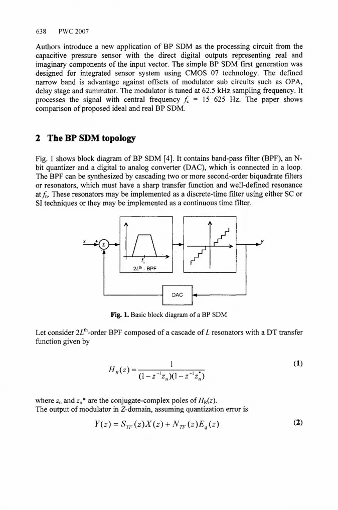
2 The BP SDM topology
Fig. 1 shows block diagram of BP SDM [4]. It contains band-pass filter (BPF), an N-bit quantizer and a digital to analog converter (DAC), which is connected in a loop. The BPF can be synthesized by cascading two or more second-order biquadrate filters or resonators, which must have a sharp transfer fimction and well-defined resonance at/i- These resonators may be implemented as a discrete-time filter using either SC or SI techniques or they may be implemented as a continuous time filter.
Fig. 1. Basic block diagram of a BP SDM
Let consider 2Z*-order BPF composed of a cascade of I resonators with a DT transfer fiinction given by
H,iz) = 1 (1)
(i-z-'z„)(]-z-'z:) where Zn and Zn* are the conjugate-complex poles of//R(Z). The output of modulator in Z-domain, assuming quantization error is
Y{z) = S,, {z)X{z) + N,, (z)E^ (z) (2)

Personal Wireless Communications 639
The signal transfer ftinction (STF) and noise transfer function (NTF) are as follows
S,,iz) = [NA^)f (3)
[N,{z) + (l-z-'z„)(l-z-'z:)f
N,Az) = [(i-z-'z„)(i-z-'z:)f
[iV,(2) + ( l - z - ' z „ ) ( l - z - ' z : ) f
(4)
The output transfer characteristics for the first generation BP SDM utilized for processing circuit is
F(z) = X(z ) . z^+£^(z ) ( l + z^) (5)
Power density after noise shaping in the spectral domain is
^NS if)-f
fs l + cos
V
(6)
s J
The Fig. 2 shows the capacitive pressure sensor where one branch is sensing branch and another is reference branch.
Fig. 2. Measurement chain with BP SDM
While the pressure influences the capacity ACx the humidity knpacts the conductivity AGx of the sensing branch. Pre-processing circuit with BP SDM converts it after synchronized down-conversion into its real and imaginary part. The binary flows are converted into digital number in two digital low pass (D-LP) filters. The digital resolution is proportional to the time window of the D-LP filter. The BP SDM is

640 PWC 2007
controlled coherently with the input source frequency. The digital output values are determined by the quantized vectors in all three switch positions as follows
U, = RU\ja){C^ + ^C^ ) + G^ + ̂ G^ ] (7)
U, =RU
The phase shift of the processing block is suppressed by the subtracting operation. The difference of the digital values from the output of the LP filter in the position 1 and 2 normalized to the value measured in the position 3 is expressed by the formula. Here measured changes of capacity and resistance are obtained
The BP SDM is tuned on 62,5 kHz of sampling frequency as mentioned, it means that central frequency is
' 4 4
Formula (6) shows the minimal value of the noise shaped power density around the central frequency^c-
3 Design of auxiliary stages
This chapter describes the design procedure of generator of harmonic signal and phase locked loop (PLL).
3.1 Generator of input harmonic signal utilizing sigma-delta modulation
The digital design has been used for simplicity of chip realization. The sine wave signal is generated by means of digital sigma-delta modulation. The output from sigma-delta modulator is connected to analog low pass filter. The output sine wave signal is obtained after high frequency filtering. The input clock frequency of digital part is 4 MHz. This frequency is common for all digital stages. The digital part is proposed using VHDL language. The whole system consists of four blocks as can be seen from Fig. 3.

Personal Wireless Communications 641
digital pattern
1 01101001 1 1 11010011 1
i H
sigma-delta modulator
12:-A 1
lowpass filter
1 "A 1 output
^\T
Fig. 3. Generator block diagram
Thanks to this condition, the design is very flexible and each part could be changed very easily. The first stage of this proposal is generator of digital image of output sine wave signal, which is described in VHDL language. The core of the whole generator consists of sigma-delta modulator. The first order modulator is used for simplicity of design. The modulator (Fig. 4) includes summator and subtractor. The input and output signals are connected on it. The difference (sum) is connected to the register. The value in this register is increased at each clock pulse. The register output is compared in comparator zero reference value. In case when register value is higher than zero, the comparator reverse into logic high, in other cases is zero. The comparator output is modulated sine wave signal. It could be filtered and analog signal could be obtained. The output is directly connected to the analog low-pass filter.
CLK
Q7 (modulated signal)
Q7-Q0
Fig. 4. The block diagram of sigma-delta modulator
The modulator realization is shown on Fig. 4. This whole part (fi'om look-up memory ROM till output) is programmed in VHDL. The comparator has been replaced by MSB of register for simplicity, because the decision level of comparator has been set at binary number 64, which is zero reference value. Thanks to this modification, the design is sign-less. The last stage is low-pass filter. It is only analog part of the whole proposal. This filter has been designed separately. It has been chosen third order active Butterworth RC filter with cut-off frequency of 15 625 Hz. The filter makes analog signal from modulated signal The digital stages have been designed in VHDL language in Xilinx ISE WebPack design environment. The simulation (Fig. 5) proceed in simulation program ModelSim Xilinx Edition. The main aim was to obtain as simple control logic as

642 PWC 2007
possible because of chip area. The design has been tested and finalized in FPGA Spartan-3.
Fig. 5. The simulation of digital stage function
The analog part is low-pass filter. First the simple RC filter has been used and its fimction has been verified. Then the third order RC filter has been utilized with exact frequency of 15 625 Hz. The 4 MHz frequency of pulses at modulator output is obtained. Therefore this filter should be allowed to separate sine wave signal from digital noise at the output sufficiently. Filter consists of one fast OPA.
3.2 Design of PLL
The PLL stage is designed utilizing well-known structures, which is shown on Fig. 6. The input sinewave signal is converted by means of comparator onto pulses. Than phase detector, which is bipolar charge pump compares phase between these pulses and signal generated by VCO (Voltage Controlled Oscillator).
xit)
Knr. = 2,5 V com '
[>> ^
^ ^
^
•A
phase detector w
-̂
VCO
f,„, = 62,5 kHz
Ml "^ ^
Fig. 6. Block diagram of designed PLL
The VCO is designed as starving ring oscillator with current controlled invertors as shown in Fig. 7.

Personal Wireless Communications 643
Fig. 7. Schematic diagram of VCO
The VCO is designed for 25 ^A driving current at control voltage 1.3 V. The ring oscillator consists of 5 controlled invertors. Since the output frequency has to be very low, there are used capacitors to produce the time delay.
The phase detector (PD) detects the phase difference between the reference signal and the feedback signal from the VCO and frequency divider. Note that, although the PD of a PLL can be an analog multiplier, an exclusive-or (XOR) gate or a J-K flip-flop, etc, for a frequency synthesizer we always use the charge-pump PLL with a tri-state phase-frequency detector (PFD) that also detects frequency errors.
4 Modeling of PLL with generator of input harmonic signal
The PLL with generator of harmonic signal utilizing sigma-delta modulation was designed and simulated in MATLAB SIMULINK and ModelSim. Model of generator of input harmonic signal and additional synchronizing digital logic are described in VHDL language. Output signal of generator is filtered by low pass filter. This filtered signal is led to comparator. Comparator output is feedback signal to VHDL model of generator. This feedback signal is represented as synchronization signal. Proposed model of PLL with generator of harmonic signal utilizing sigma-delta modulation is shown in Fig. 8.

644 PWC 2007
1 .fj lj<!-*ii!» U
^ i»*w«5«»»iraf«^
Fig. 8. Model of PLL with generator of input harmonic signal utilizing sigma-delta modulation
Matlab simulation results of PLL with generator of harmonic signal utilizing sigma-delta modulation is shown on Fig. 9. Modelsim simulation results of PLL with generator of harmonic signal utilizing sigma-delta modulation is shown on fig. 10.
5.00E-05
Fig. 9. Matlab simulation results of PLL with generator of harmonic signal utilizing sigma-delta modulation
Fig« 10. ModelSim simulation results of PLL with generator of harmonic signal utilizing sigma-delta modulation

Personal Wireless Communications 645
5 Design of band-pass modulator in Cadence
The switching of the inputs is synchronized with internal switching of modulator since it uses blocks with SC technique. The ideal BP SDM consists of input S/H circuit, summator, four delay circuits, comparator and DAC connected in closed loop. There are several addition stages mainly D flip-flop and XOR logic gate. These stages are utilized to satisfy clock synchronization with driving clock. It is important to note that ideal BP SDM uses ideal OPAs (voltage controlled voltage source with very high gain), ideal capacitors and it has no offsets, noise sources etc. The behavior of modulator has been simulated with input signal frequency 15625 Hz with sweeped amplitude from 0 to 1 V. The computed values are average values of logic 1 and logic 0 (represented as 5 V and 0 V respectively). It means that number on y axis is ratio between logic levels appropriate to input amplitude. The most important output is XOR output. It can be seen that this output is quite linear and appropriate to input amplitude. The beginning of the curves is affected by start-up phase of modulator and should not be considered. The real BP SDM circuitry is depicted on Fig. 11.
Fig. 11. Block diagram of real BP SDM
The delay and S/H circuits are designed in SC technique. Comparator is proposed with latch„ The DAC is simple 1-bit circuit. This modulator has been designed and simulated in Cadence software using CMOS 07 technology. The power supply is 5 V. The systematic offset of the basic loop is 140 \iV. Since this is the first realization of that kind of chip for capacitive pressure sensors, there are many auxiliary pins used for testing measurement. The aim of this arrangement is to obtain maximum information about behaviour of each stage of BP SDM. The most critical parts are blocks using switched-capacitor approach, because there are many nonidealities and error sources, mainly clock feedthrough and noise« Table L lists all pins, which will be led out of the chip for testing.

646 PWC 2007
Tab. 1. Expected list of pins for 24-DIL package
Pin no.
1
2
3
4
5
6
7
8
9
10
11
12
13
14
15
16
17
18
19
20
21
22
23
1 24
Name
vss
VSSA
VDDA
OUT SH
IN
REZ IN
DAC OUT
REZ OUT
AGND
NREF
PREF
PH2 n
PH2
PHI n
PHI
OUT D
OUT XOR
CLK
KOMP OUT
VDD
Description
not used
input
input
input
output
input
output
output
not used
output
input
input
not used
input
output
output
output
output
output
output
not used
input
output
input
Function |
supply of digital part
supply of analog part
supply of analog part
output of S/H circuit
analog input
output of summator
output of DAC
output of delay circuits
analog ground
negative reference voltage of DAC |
positive reference voltage of DAC |
output of nonoverlapping clock PH2 n
output of nonoverlapping clock PH2 |
output ofnonoverlapping clock PHI n
output of nonoverlapping clock PH1 |
output of D flip-flop 1
output of XOR (most important) 1
input of X-tal clock |
output of comparator 1
supply of digital part |
The average outputs of real BP SDM depending on magnitude of analog input signal (range from 0 to 1 V) are shown on Fig. 12. It can be seen, that output of XOR is mostly linear, which is expected result. Consequently the output plots of real BP SDM correspond with ideal one, so the proposed V^ generation BP SDM for pressure sensing works correctly.

Personal Wireless Communications 647
3.60
3,40
3.20
3.00
2.80
2.60
2.40
3.90
3.60
3.30
3.00
2.70
2.40
ovr.. D
• : ovr„komp
Fig. 12. Output plots of real BP SDM
6 Conclusions
The BP SDMs are well suited for wireless applications. This paper shows another way how to use its advantages. Authors designed 1st generation BP SDM as preprocessing block for capacitive pressure sensing. The behavior of real modulator has been verified and compared. Two possibilities of PLL design are presented in this paper. Both solutions will be designed on ASIC. The first one is conventional approach which is shown on fig. 6. The second one uses digital sigma-delta modulator as generator of input harmonic signal. This part with additional synchronizing digital logic is described by VHDL language. This digital part will be implemented on chip by using Synthesis and Place&Route tools. Matlab modeling of PLL with digital sigma-delta modulator is presented in this paper. Moreover, the test results will serve

648 PWC 2007
to the chip redesign targeted on the improvement of the conversion accuracy and the reduction of the power consumption.
Acknowledgments The research has been supported by the Czech Ministry of Education in the frame of Research Program MSM0021630503 MICROSYN, by the Czech Grant Agency as the project GA102/03/0619 Smart Microsensors and Microsystems for Measurement and Regulation and project GA 102/05/0869.
References
1. Ong, A., K., Wooley, B., A. A Two-Path Bandpass SD Modulator for Digital IF Extraction at 20 MHz, IEEE Journal of Solid-State Circuits, vol. 32, No. 12, December, 1997
2. Lao, CH., Leong, H., Au, K., Mok, K., U, S., Martins, R., P. A 10.7-MHz Bandpass Sigma-Delta Modulator Using Double-Delay Single-opamp SC Resonator with Double-Sampling,
3. Tabatabaei, A.̂ Wooley, B., A. A Two-Path Bandpass Sigma-Delta Modulator with Extended Noise Shaping, IEEE Journal of Solid-State Circuits, vol. 35, No. 12, December, 2000
4. Rodrigez-Vazquez, A., Madeiro, F., Janssens, E. CMOS Telecom Data Converters, Springer Verlag, 2004, 375 pages, ISBN 1402075464
5. Shu, K., Sanchez-Sinenco, E., CMOS PLL Synthesizers, Analysis and Design, Springer Science, 2005, 232 pages, ISBN 0-387-23669-4


