Embed Size (px)
Citation preview
1
MODULE -4 Sub system design and PLA
ACSCE
ACSCE DR.HBB notes on VLSI
SYSTEM and SUB SYSTEM
• System is a set of interdependent entities/modules /leaf cell which interact
among themselves to form a complete unit.
• Large systems are composed of subsystems known as leaf cells.
• Most basic leaf cells are inverter, NAND,CMOS ….
2ACSCE DR.HBB notes on VLSI
3
A system
ACSCE DR.HBB notes on VLSI
ARCHITECTURAL ISSUES OF SUBSYSTEM DESIGN• In any VLSI system, logical and systematic approach is essential.
For ex:
In designing an MSI logic circuit comprising of
a) 500 transistors - 2 engineer-months are required, similarly in designing b) 500,000 transistor - 2,000 engineer-months or 170-engineers - years are required.
• Thus as complexity increases, design time exponentially increases.
Therefore,
we must adopt design methods which handle complexity
with a less time and
with less labor.
4ACSCE DR.HBB notes on VLSI
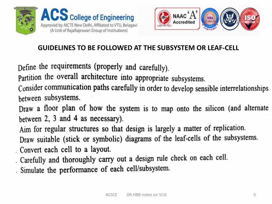
GUIDELINES TO BE FOLLOWED AT THE SUBSYSTEM OR LEAF-CELL
5ACSCE DR.HBB notes on VLSI
6ACSCE DR.HBB notes on VLSI
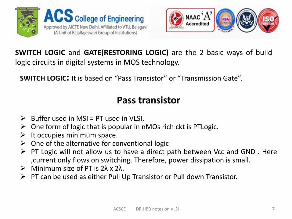
SWITCH LOGIC and GATE(RESTORING LOGIC) are the 2 basic ways of buildlogic circuits in digital systems in MOS technology.
SWITCH LOGIC: It is based on “Pass Transistor” or “Transmission Gate”.
Pass transistor
➢ Buffer used in MSI = PT used in VLSI.➢ One form of logic that is popular in nMOs rich ckt is PTLogic.➢ It occupies minimum space.➢ One of the alternative for conventional logic➢ PT Logic will not allow us to have a direct path between Vcc and GND . Here
,current only flows on switching. Therefore, power dissipation is small.➢ Minimum size of PT is 2λ x 2λ.➢ PT can be used as either Pull Up Transistor or Pull down Transistor.
7ACSCE DR.HBB notes on VLSI
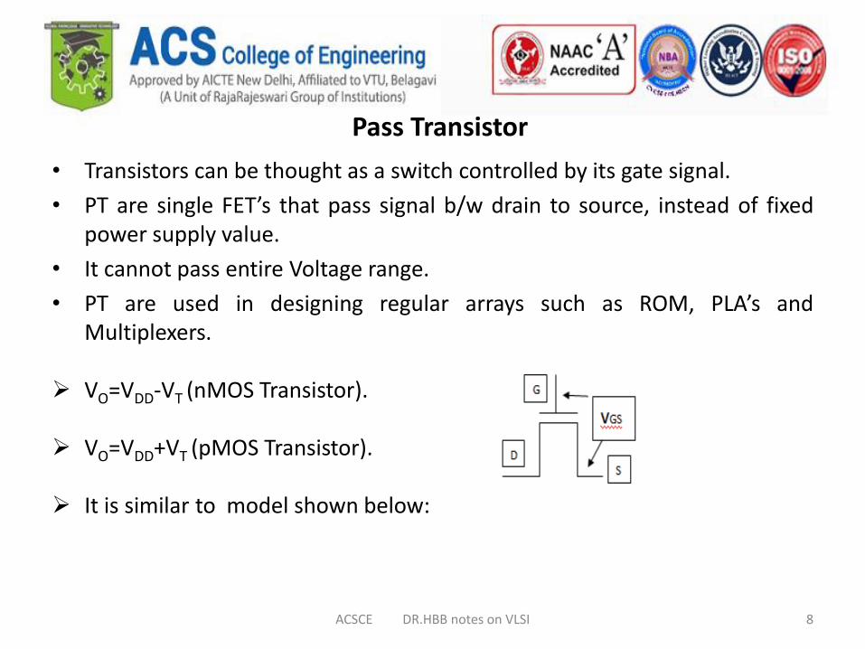
Pass Transistor
• Transistors can be thought as a switch controlled by its gate signal.
• PT are single FET’s that pass signal b/w drain to source, instead of fixedpower supply value.
• It cannot pass entire Voltage range.
• PT are used in designing regular arrays such as ROM, PLA’s andMultiplexers.
➢ VO=VDD-VT (nMOS Transistor).
➢ VO=VDD+VT (pMOS Transistor).
➢ It is similar to model shown below:
8ACSCE DR.HBB notes on VLSI
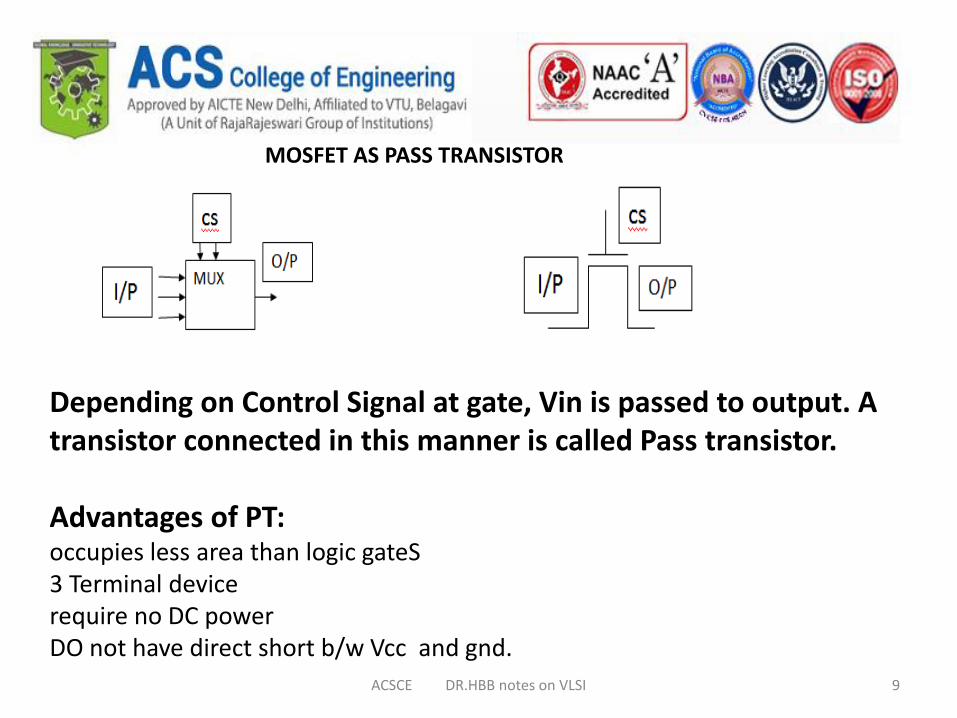
Depending on Control Signal at gate, Vin is passed to output. A transistor connected in this manner is called Pass transistor.
Advantages of PT:occupies less area than logic gateS3 Terminal device require no DC powerDO not have direct short b/w Vcc and gnd.
9
MOSFET AS PASS TRANSISTOR
ACSCE DR.HBB notes on VLSI
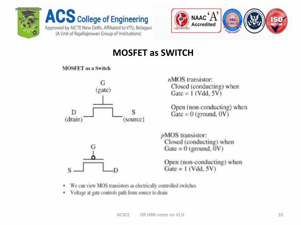
MOSFET as SWITCH
10ACSCE DR.HBB notes on VLSI
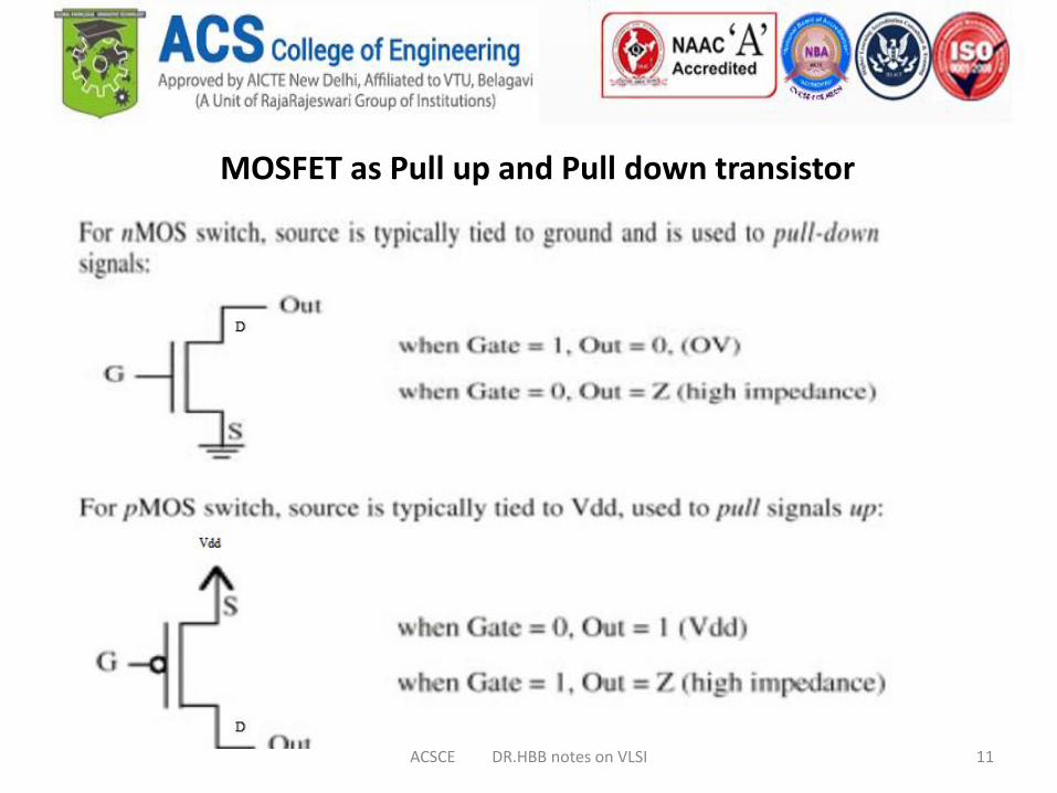
MOSFET as Pull up and Pull down transistor
11ACSCE DR.HBB notes on VLSI
12
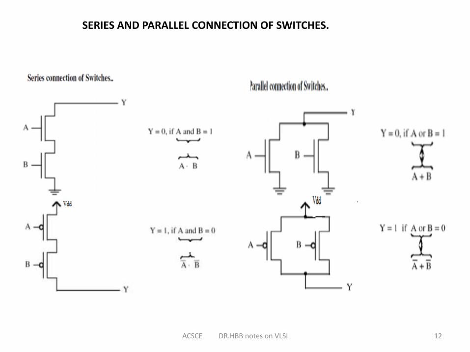
SERIES AND PARALLEL CONNECTION OF SWITCHES.
ACSCE DR.HBB notes on VLSI
Slide 13
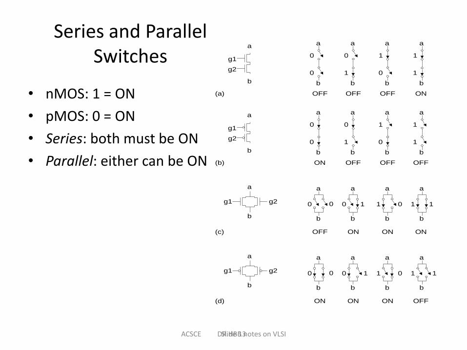
Series and Parallel Switches
• nMOS: 1 = ON
• pMOS: 0 = ON
• Series: both must be ON
• Parallel: either can be ON
(a)
a
b
a
b
g1
g2
0
0
a
b
0
1
a
b
1
0
a
b
1
1
OFF OFF OFF ON
(b)
a
b
a
b
g1
g2
0
0
a
b
0
1
a
b
1
0
a
b
1
1
ON OFF OFF OFF
(c)
a
b
a
b
g1 g2 0 0
OFF ON ON ON
(d) ON ON ON OFF
a
b
0
a
b
1
a
b
11 0 1
a
b
0 0
a
b
0
a
b
1
a
b
11 0 1
a
b
g1 g2
ACSCE DR.HBB notes on VLSI
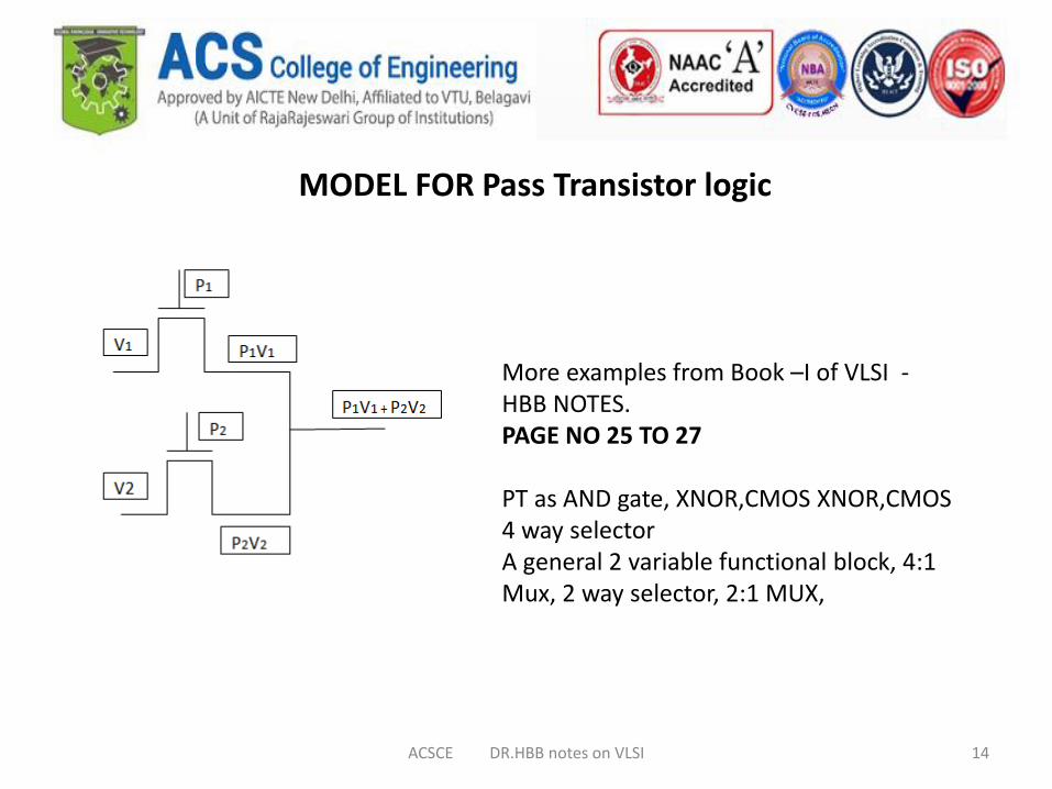
MODEL FOR Pass Transistor logic
14
More examples from Book –I of VLSI -HBB NOTES. PAGE NO 25 TO 27
PT as AND gate, XNOR,CMOS XNOR,CMOS 4 way selectorA general 2 variable functional block, 4:1 Mux, 2 way selector, 2:1 MUX,
ACSCE DR.HBB notes on VLSI
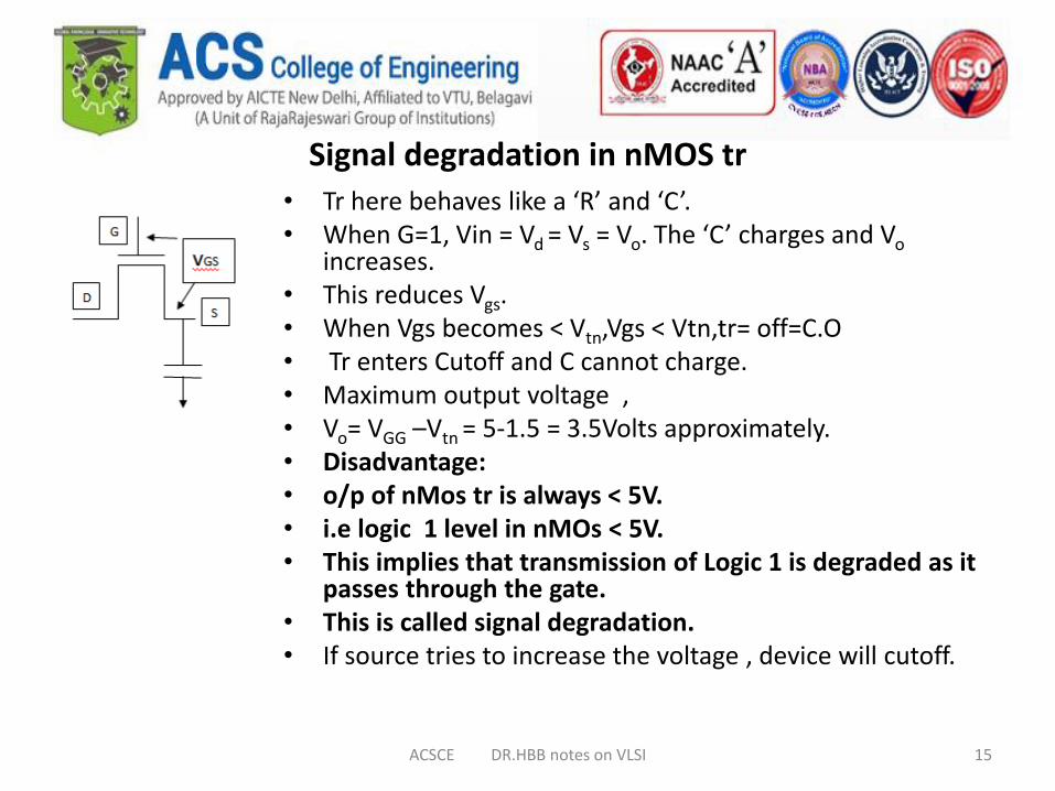
Signal degradation in nMOS tr
• Tr here behaves like a ‘R’ and ‘C’. • When G=1, Vin = Vd = Vs = Vo. The ‘C’ charges and Vo
increases.• This reduces Vgs.• When Vgs becomes < Vtn,Vgs < Vtn,tr= off=C.O• Tr enters Cutoff and C cannot charge.• Maximum output voltage ,• Vo= VGG –Vtn = 5-1.5 = 3.5Volts approximately.• Disadvantage:• o/p of nMos tr is always < 5V.• i.e logic 1 level in nMOs < 5V.• This implies that transmission of Logic 1 is degraded as it
passes through the gate.• This is called signal degradation.• If source tries to increase the voltage , device will cutoff.
15ACSCE DR.HBB notes on VLSI
Page 17 , book -1nMOS:• An nMOS transistor is an almost
perfect switch when passing a 0and thus we say it passes a strong0.
• However, the nMOS transistor isimperfect at passing a 1. The high
• voltage level is somewhat lessthan V DD . We say it
• passes a degraded or weak signal.Transmission of Logic 1 isdegraded as it passes through thenmos.
VO=VDD-VT (nMOS tr.)• Vin = 0 , Vo= 0 - 0.7 = - 0.7• Vin= 5, Vout = 4.3 < 5 VNmos is bad in transmitting ‘1’ or
5V and good at transmitting zero.
pMOS• Transmission of Logic 0 is degraded
as it passes through the p device.VO=VDD+ VT
• Vin = 0 , Vo=0+0.7 = 0.7• Vin= 5,Vout = 5.7 >5 V• pMOS tr is good at transmitting ‘1’
and bad in transmitting ‘0 ‘.• A pMOS transistor again has the
opposite behavior, passing• strong 1s but degraded 0s.
16ACSCE DR.HBB notes on VLSI
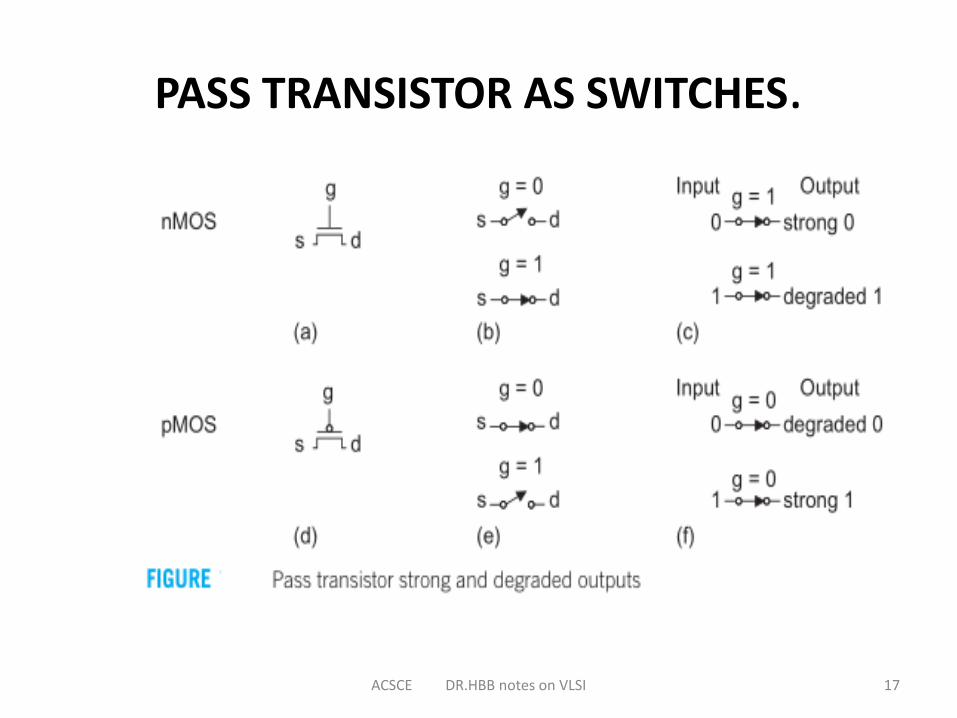
PASS TRANSISTOR AS SWITCHES.
17ACSCE DR.HBB notes on VLSI
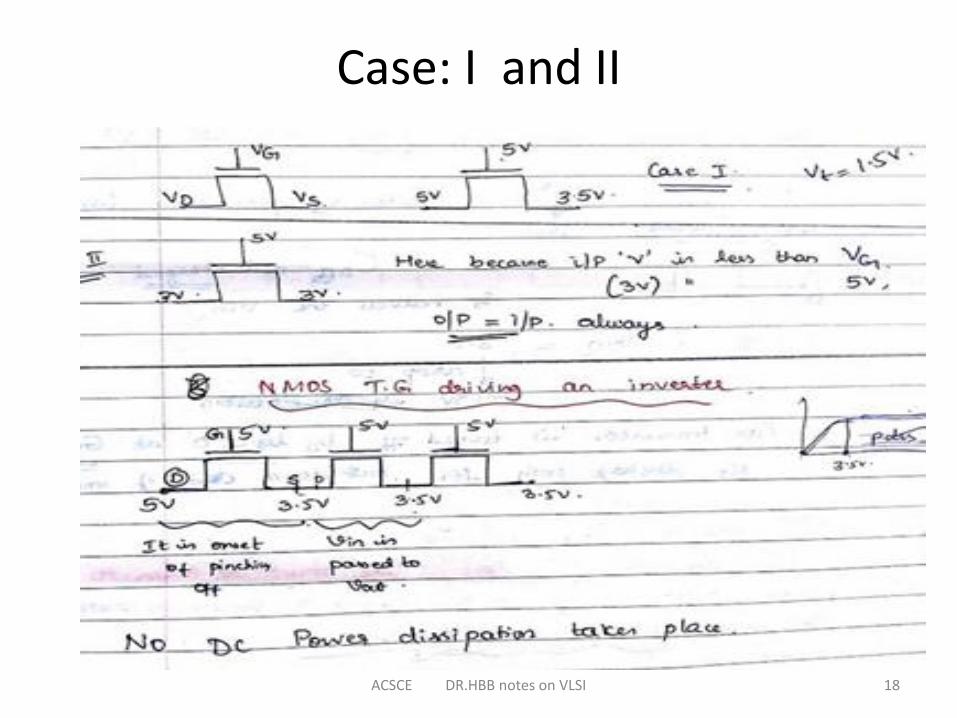
Case: I and II
18ACSCE DR.HBB notes on VLSI
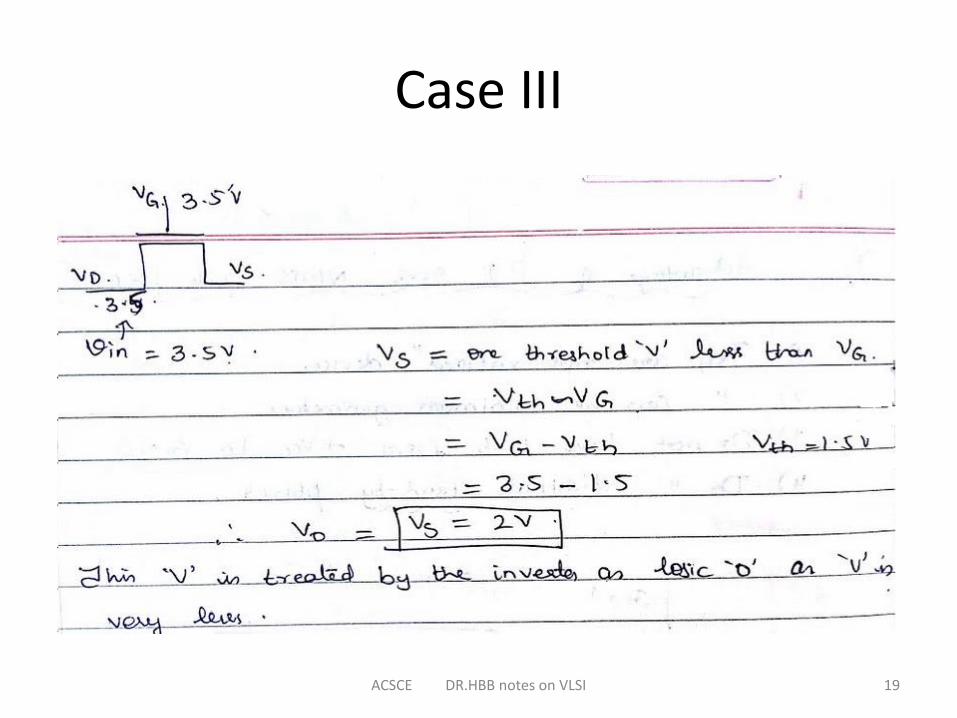
Case III
19ACSCE DR.HBB notes on VLSI
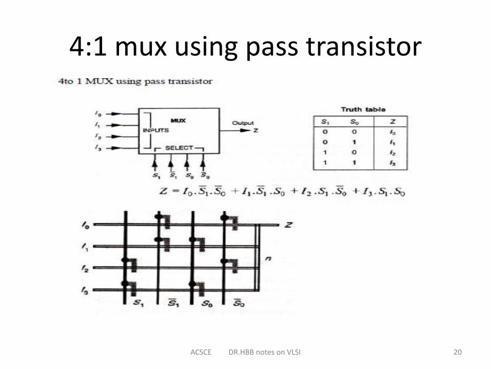
4:1 mux using pass transistor
20ACSCE DR.HBB notes on VLSI
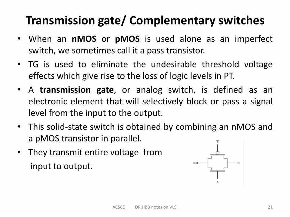
Transmission gate/ Complementary switches
• When an nMOS or pMOS is used alone as an imperfectswitch, we sometimes call it a pass transistor.
• TG is used to eliminate the undesirable threshold voltageeffects which give rise to the loss of logic levels in PT.
• A transmission gate, or analog switch, is defined as anelectronic element that will selectively block or pass a signallevel from the input to the output.
• This solid-state switch is obtained by combining an nMOS anda pMOS transistor in parallel.
• They transmit entire voltage from
input to output.
21ACSCE DR.HBB notes on VLSI
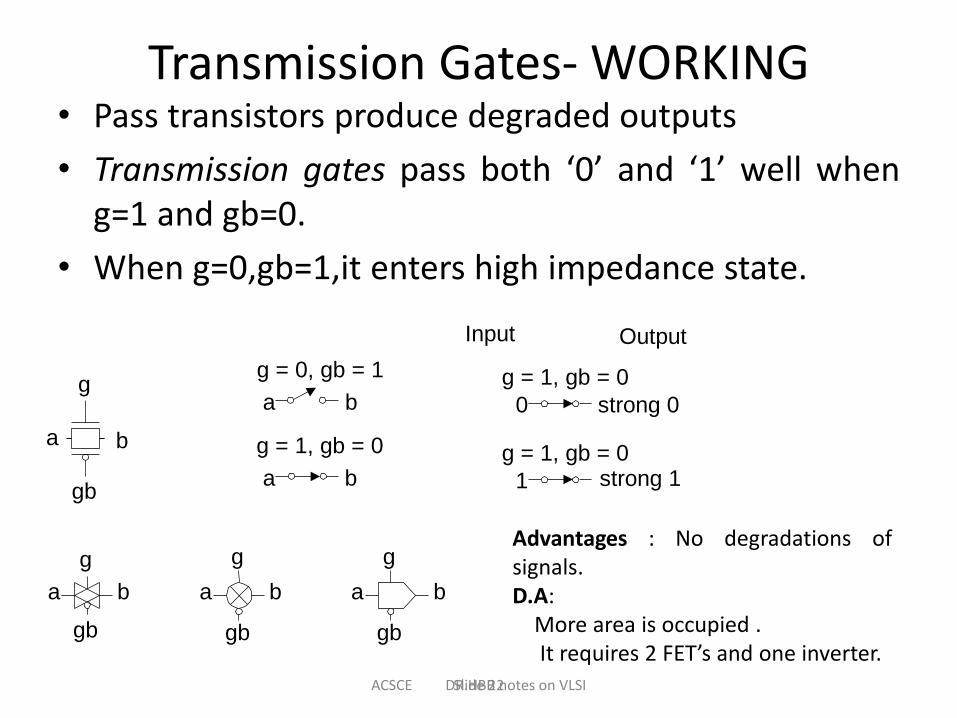
Slide 22
Transmission Gates- WORKING• Pass transistors produce degraded outputs
• Transmission gates pass both ‘0’ and ‘1’ well wheng=1 and gb=0.
• When g=0,gb=1,it enters high impedance state.
g = 0, gb = 1
a b
g = 1, gb = 0
a b
0 strong 0
Input Output
1 strong 1
g
gb
a b
a b
g
gb
a b
g
gb
a b
g
gb
g = 1, gb = 0
g = 1, gb = 0
Advantages : No degradations ofsignals.D.A:
More area is occupied .It requires 2 FET’s and one inverter.
ACSCE DR.HBB notes on VLSI
GATE (restoring LOGIC)• It is based on general arrangements circuits.
• Ex: Inverter ,NAND,NOR and OR.
23ACSCE DR.HBB notes on VLSI
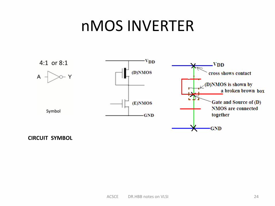
nMOS INVERTER
24
CIRCUIT SYMBOL
4:1 or 8:1
ACSCE DR.HBB notes on VLSI
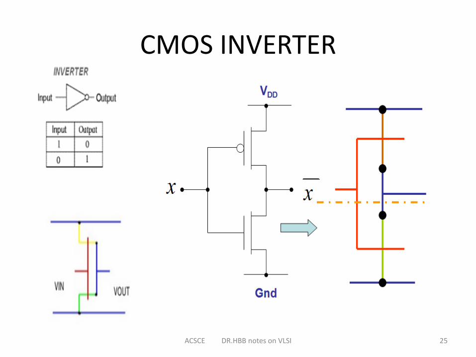
CMOS INVERTER
25ACSCE DR.HBB notes on VLSI
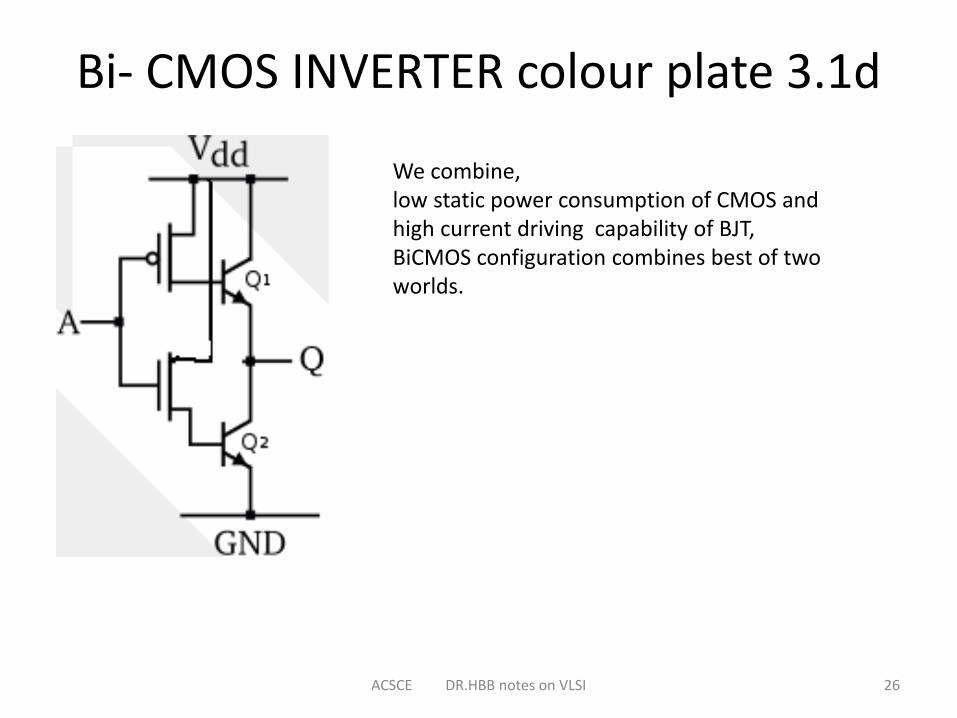
Bi- CMOS INVERTER colour plate 3.1d
26
We combine, low static power consumption of CMOS and high current driving capability of BJT, BiCMOS configuration combines best of two worlds.
ACSCE DR.HBB notes on VLSI
Page number 20,21, book- 1 vlsi
• Nand gate
• Nor gate
27ACSCE DR.HBB notes on VLSI
Examples for structured design( Combinational logic)
28ACSCE DR.HBB notes on VLSI
PARITY GENERATOR ( PG)- Basics • It is a concept to detect errors.
• A parity bit is commonly used for error detection during thetransmission of digital signals.
• Parity systems: Odd parity and Even parity
• Parity bit is added to original message signal to make it eithereven or odd parity.
• Exclusive-OR and exclusive-NOR gates are used in applicationssuch as parity checking, binary comparison and controlledcomplementing circuits.
• Electrical noise in the transmission of binary information can cause errors. Parity can detect these types of errors.
29ACSCE DR.HBB notes on VLSI
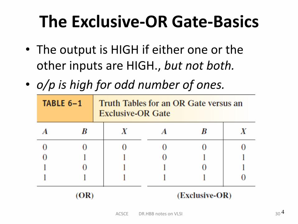
The Exclusive-OR Gate-Basics
• The output is HIGH if either one or the other inputs are HIGH., but not both.
• o/p is high for odd number of ones.
430ACSCE DR.HBB notes on VLSI
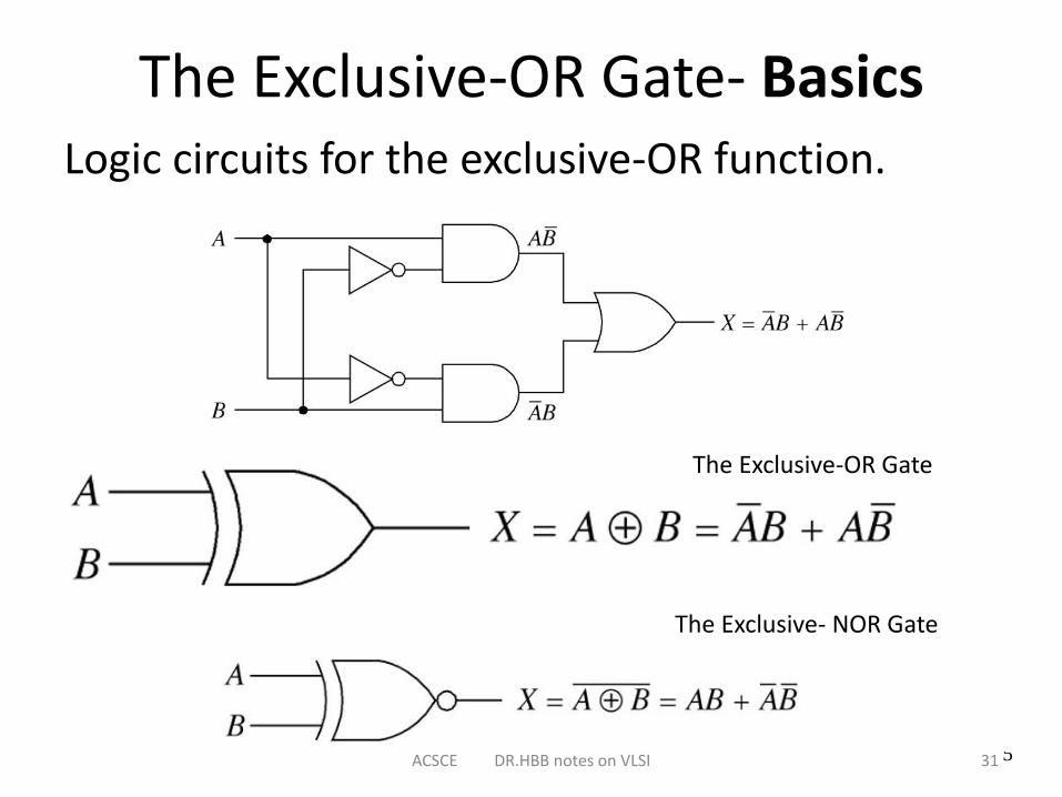
The Exclusive-OR Gate- BasicsLogic circuits for the exclusive-OR function.
5
The Exclusive-OR Gate
The Exclusive- NOR Gate
31ACSCE DR.HBB notes on VLSI
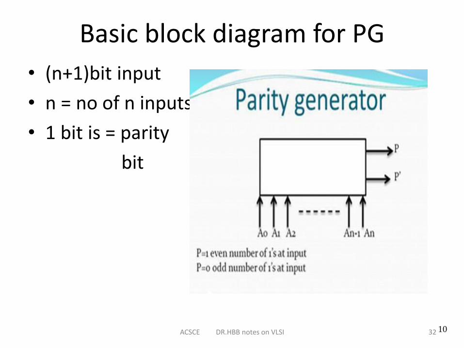
Basic block diagram for PG
• (n+1)bit input
• n = no of n inputs
• 1 bit is = parity
bit
1032ACSCE DR.HBB notes on VLSI
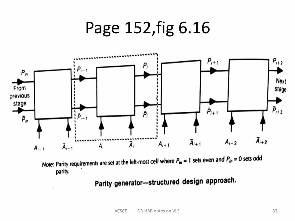
Page 152,fig 6.16
33ACSCE DR.HBB notes on VLSI
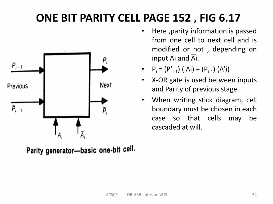
ONE BIT PARITY CELL PAGE 152 , FIG 6.17 • Here ,parity information is passed
from one cell to next cell and ismodified or not , depending oninput Ai and Ai.
• Pi = (P’i-1) ( Ai) + (Pi-1) (A’i)
• X-OR gate is used between inputsand Parity of previous stage.
• When writing stick diagram, cellboundary must be chosen in eachcase so that cells may becascaded at will.
34ACSCE DR.HBB notes on VLSI
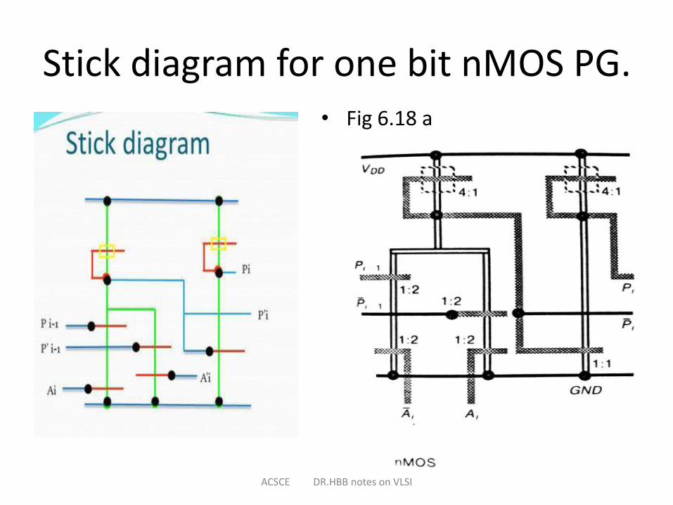
Stick diagram for one bit nMOS PG.• Fig 6.18 a
35
ACSCE DR.HBB notes on VLSI
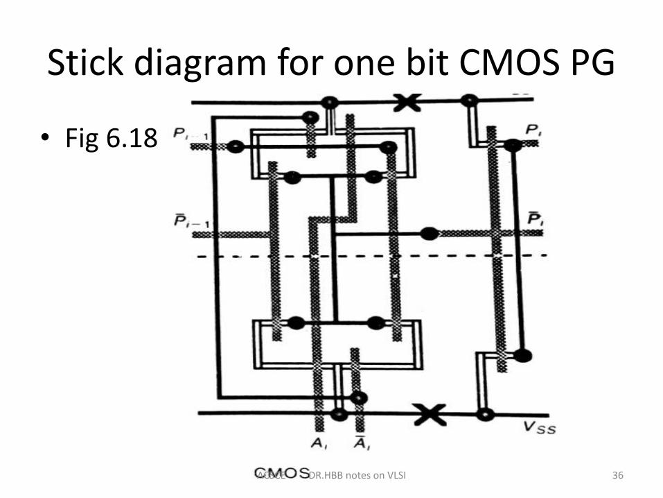
Stick diagram for one bit CMOS PG
• Fig 6.18b
36ACSCE DR.HBB notes on VLSI
MULTIPLEXER / DATA SELECTOR• The multiplexer OR “MUX” is a combinational logic circuit
designed to switch one of several input lines through to asingle common output line by the application of a controlsignal.
• It can be either digital circuits or analogue types usingtransistors, MOSFET’s or relays to switch one of the voltage orcurrent inputs through to a single output.
• They are available in a number of standard configuration inTTL or other logic families.
37ACSCE DR.HBB notes on VLSI
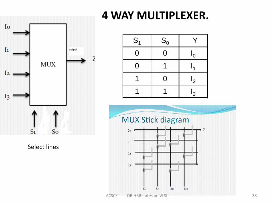
4 WAY MULTIPLEXER.
38
S1 S0 Y
0 0 I0
0 1 I1
1 0 I2
1 1 I3
Select lines
ACSCE DR.HBB notes on VLSI
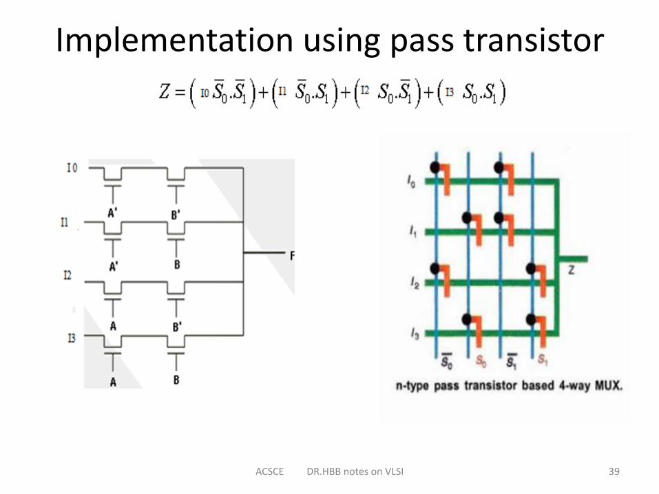
Implementation using pass transistor
39ACSCE DR.HBB notes on VLSI
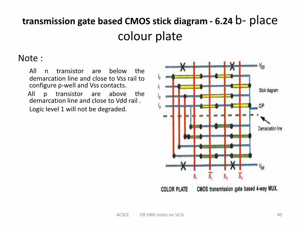
transmission gate based CMOS stick diagram - 6.24 b- place colour plate
Note : All n transistor are below thedemarcation line and close to Vss rail toconfigure p-well and Vss contacts.All p transistor are above thedemarcation line and close to Vdd rail .Logic level 1 will not be degraded.
40ACSCE DR.HBB notes on VLSI
41
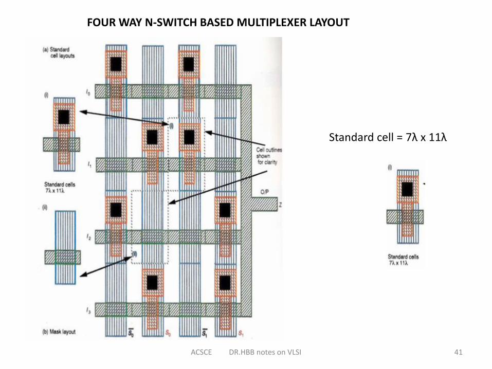
FOUR WAY N-SWITCH BASED MULTIPLEXER LAYOUT
Standard cell = 7λ x 11λ
ACSCE DR.HBB notes on VLSI
PLA – Programmable logic array
42ACSCE DR.HBB notes on VLSI
Contents covered - I
The Programmable Logic Array (PLA)- VLSI Design”- Douglas
A. Pucknell& Kamran Eshraghian, PHI 3rd,Edition (originalEdition – 1994). Slide 2- 11
Contents covered – IIFIELD PROGRAMMABLE GATE ARRAYS
FPGA ARCHITECTURE
PHYSICAL DESIGN OF FPGA
“FPGA Based System Design”- Wayne Wolf, Pearson Education, Technology and Engineering, 2004 . Slide 22 - 49
43ACSCE DR.HBB notes on VLSI
The Programmable Logic Array (PLA)
Text book :
“Basic VLSI Design”- Douglas A. Pucknell& Kamran Eshraghian, PHI 3rd,Edition (original Edition – 1994).
44ACSCE DR.HBB notes on VLSI
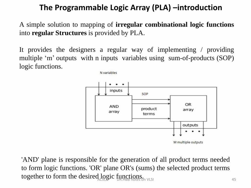
The Programmable Logic Array (PLA) –introduction
A simple solution to mapping of irregular combinational logic functions
into regular Structures is provided by PLA.
It provides the designers a regular way of implementing / providing
multiple ‘m’ outputs with n inputs variables using sum-of-products (SOP)
logic functions.
'AND' plane is responsible for the generation of all product terms needed
to form logic functions. 'OR' plane OR's (sums) the selected product terms
together to form the desired logic functions.45ACSCE DR.HBB notes on VLSI
.
The Programmable Logic Array (PLA)
▪Personalized" by making or breaking connections among the gates.
▪It performs the same basic function as a ROM.
▪Pre-fabricated building block of many AND/OR gates (or NOR, NAND).
▪It consists of two level of combinational logic functions .
▪PLA describes class of standalone devices that allows users to program the
functionalities.
▪Presently, we have PLA with 14 i/p variables, 96 product terms , 8 o/p
functions. Such elements are programmed by manufacturer or field
programmed by user to meet requirements.
▪The capability of these programmable devices are limited and have been
replaced by significantly powerful field programmable gate array (FPGA).
46ACSCE DR.HBB notes on VLSI
▪
1) In Vlsi design, however, Custom PLA’s can be readily designed and must be programmed during
the design process . Thus, for the VLSI designer , PLA’s are tailored
to specific task with little wastage of function or space .
.
2)PLA structure is normally expanded, or modified during design.
3) In vlsi design, our objectives is to map circuits onto silicon to meet specifications
Floor plan indicates PLA mapping onto chips. It also gives notional areas and relative disposition of
particular circuits and subsystems.
.
De-morgan’s theorem is used to manipulate AND-OR combinational logic requirements into NOR
form. .
47ACSCE DR.HBB notes on VLSI
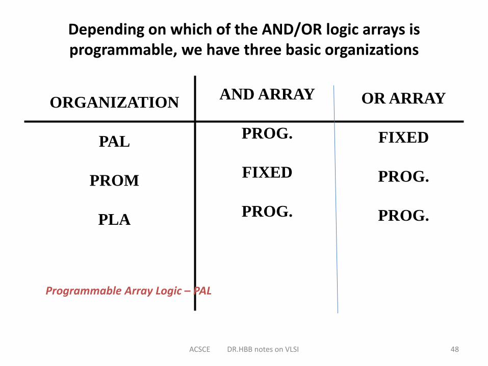
Depending on which of the AND/OR logic arrays is programmable, we have three basic organizations
AND ARRAY
PROG.
FIXED
PROG.
OR ARRAY
FIXED
PROG.
PROG.
ORGANIZATION
PAL
PROM
PLA
Programmable Array Logic – PAL
48ACSCE DR.HBB notes on VLSI
General architecture of PLA
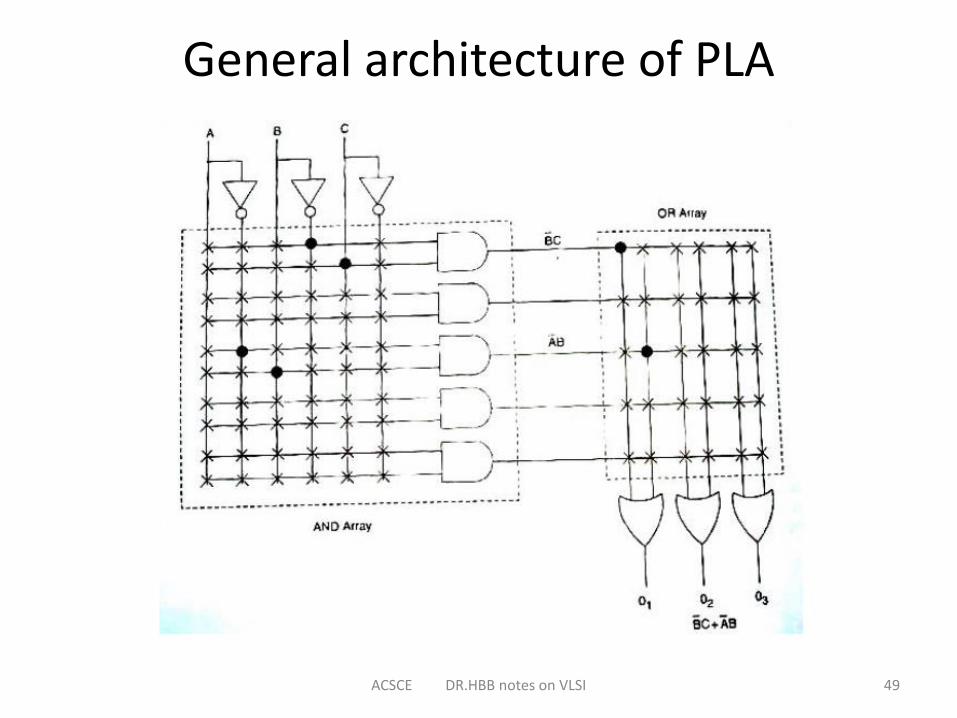
49ACSCE DR.HBB notes on VLSI
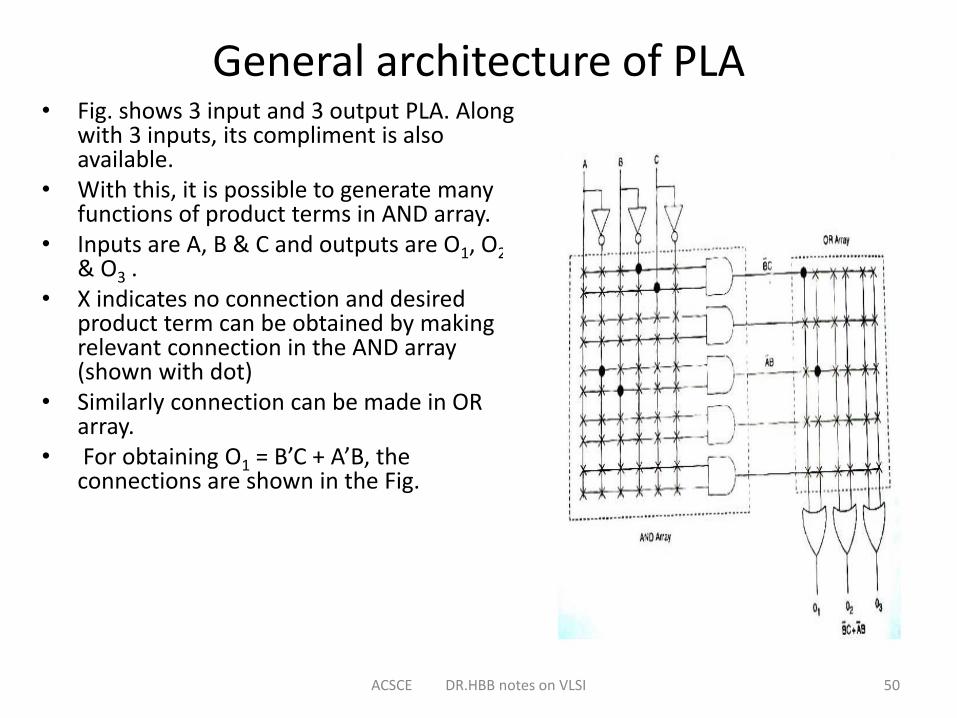
General architecture of PLA • Fig. shows 3 input and 3 output PLA. Along
with 3 inputs, its compliment is also available.
• With this, it is possible to generate many functions of product terms in AND array.
• Inputs are A, B & C and outputs are O1, O2& O3 .
• X indicates no connection and desired product term can be obtained by making relevant connection in the AND array (shown with dot)
• Similarly connection can be made in OR array.
• For obtaining O1 = B’C + A’B, the connections are shown in the Fig.
50ACSCE DR.HBB notes on VLSI
• In VLSI design, objective is to map circuits onto Si to meet thespecifications.
• In circuit implementation for AND and OR array needs NAND and NOTlogic and NOR and NOT logic respectively. But this includes morefabrication steps.
• However, this can be simplified by implementing the logic in NOR logic.Thus AND and OR array can be implemented using NOR logic.
• If the output of NOR is complimented, then we get the OR logic. Similarlyif both the inputs of AND is complimented and given to NOR it gives ANDlogic
51ACSCE DR.HBB notes on VLSI
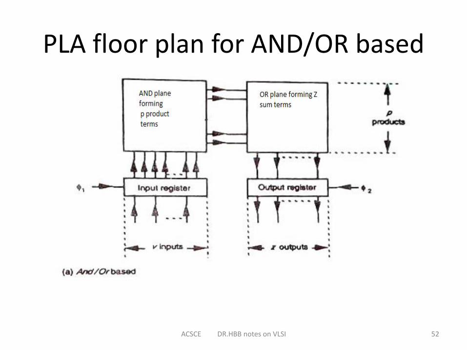
PLA floor plan for AND/OR based
52ACSCE DR.HBB notes on VLSI
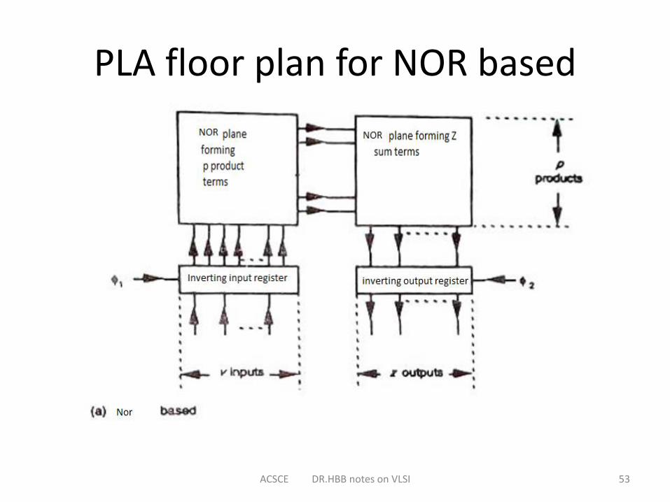
PLA floor plan for NOR based
53ACSCE DR.HBB notes on VLSI
FPGA –
FIELD PROGRAMMABLE GATE ARRAYS
“FPGA Based System Design”- Wayne Wolf, Pearson Education, Technology and
Engineering, 2004
DR.HBB . PLA - VLSI DESIGN 1
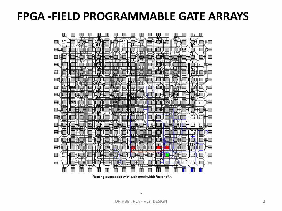
FPGA -FIELD PROGRAMMABLE GATE ARRAYS
An introduction
. DR.HBB . PLA - VLSI DESIGN 2
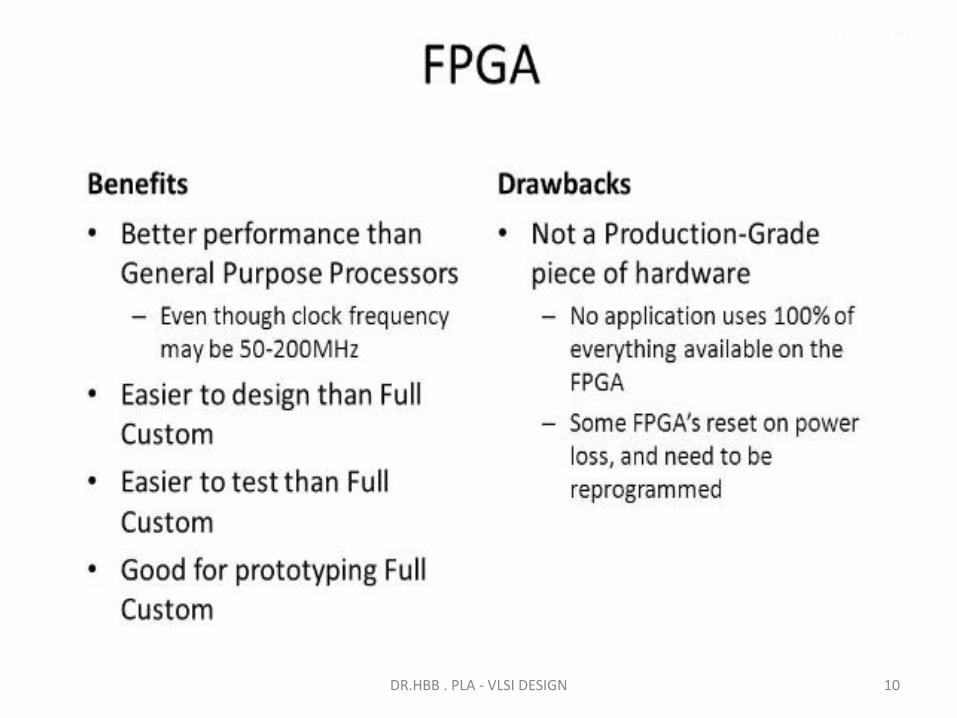
FPGA• FPGA plays the complementary role of microprocessor.
• Standard parts: They are not designed for any particularfunctions but are programmed by customer for a particularpurpose.
• Implement multilevel logic:
They use both programmable logic blocks and Programmableinterconnect to build the multi level logic functions.
• FABRIC: Combination of logic and interconnect.
• They are used in all sorts of digital systems. Because of its
a) high speed Telecommunications equipment
b) as video accelerators in home personal video recorders(PVR)’s.
• FPGA is far better than smaller programmable device likePLD’s.
DR.HBB . PLA - VLSI DESIGN 3
DR.HBB . PLA - VLSI DESIGN 4
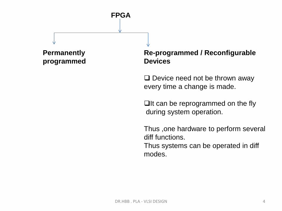
FPGA
Permanently
programmed
Re-programmed / Reconfigurable
Devices
❑ Device need not be thrown away
every time a change is made.
❑It can be reprogrammed on the fly
during system operation.
Thus ,one hardware to perform several
diff functions.
Thus systems can be operated in diff
modes.
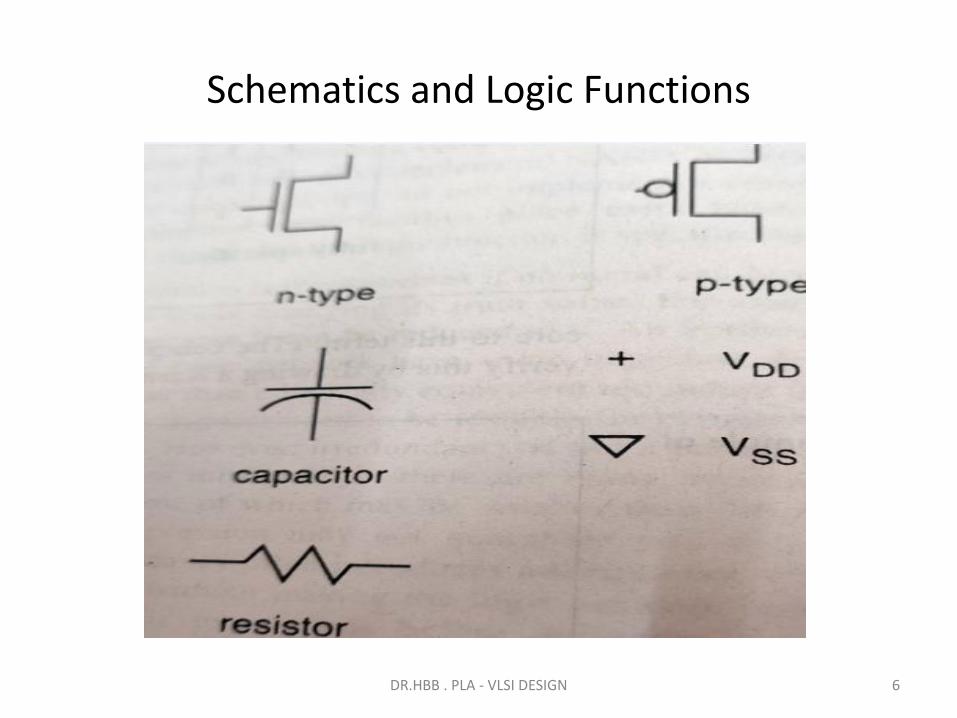
Schematics and Logic Functions
DR.HBB . PLA - VLSI DESIGN 6
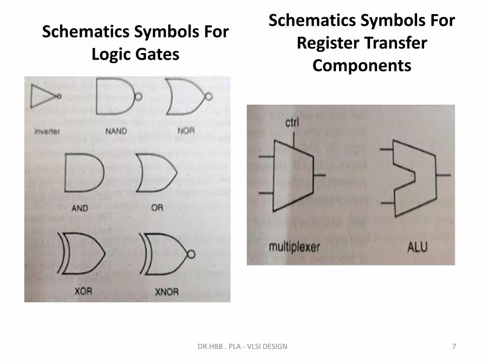
Schematics Symbols For Logic Gates
DR.HBB . PLA - VLSI DESIGN 7
Schematics Symbols For Register Transfer
Components
Digital Design and FPGAsMicroprocessor or
General Purpose operating system
• Rely on S/w to implement functions.
• Slower
• More power consumption than custom chips
FPGA /ASIC-
Application specific integrated circuit
• Not custom parts
• Slower
• Burn more power than custom logic.
• Expensive
DR.HBB . PLA - VLSI DESIGN 8
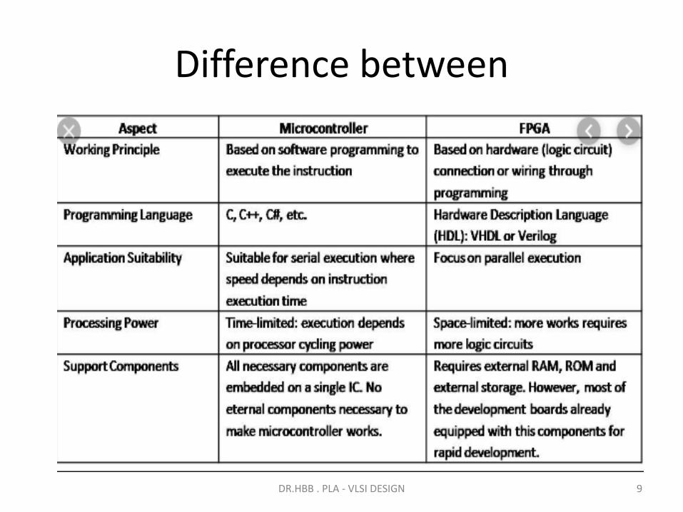
Difference between
DR.HBB . PLA - VLSI DESIGN 9
DR.HBB . PLA - VLSI DESIGN 10
DR.HBB . PLA - VLSI DESIGN 11
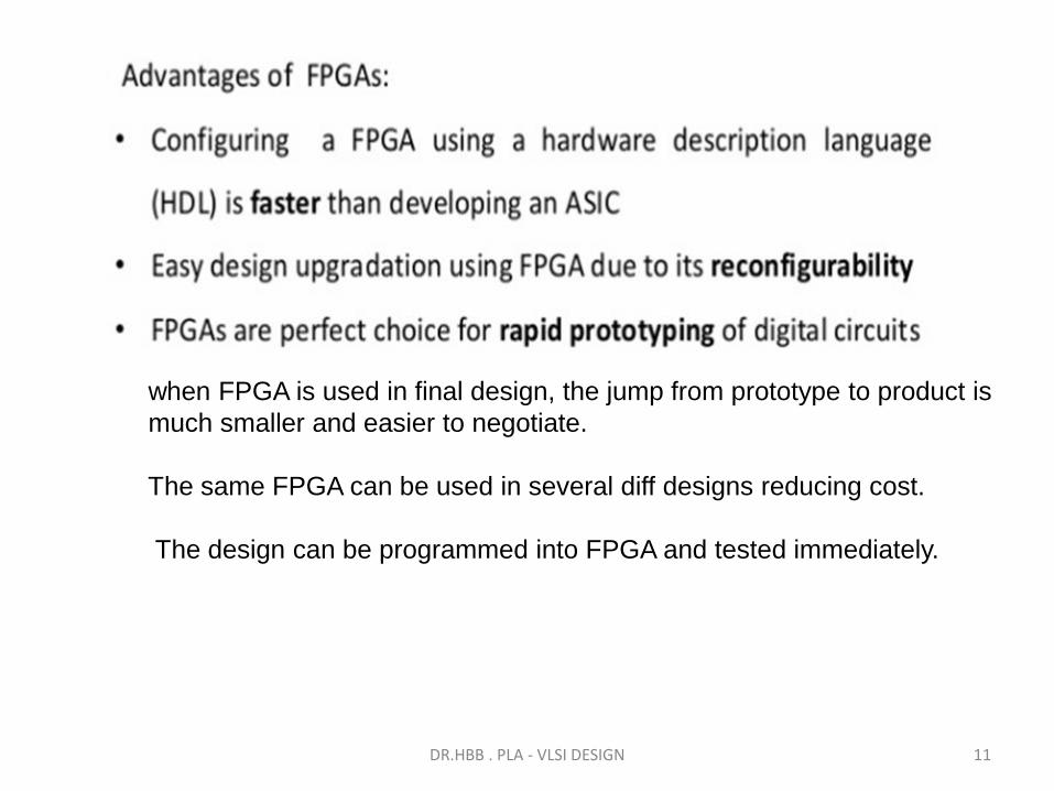
when FPGA is used in final design, the jump from prototype to product is
much smaller and easier to negotiate.
The same FPGA can be used in several diff designs reducing cost.
The design can be programmed into FPGA and tested immediately.
DR.HBB . PLA - VLSI DESIGN 12
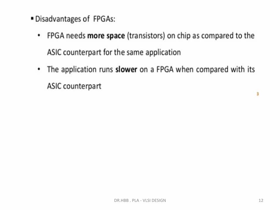
Alternative to FPGA-ASIC – Application Specific IC
• ASIC is designed to implement a particular logical function/ designed for particular purpose.
• ASIC uses predesigned layouts for logic gates.
• Design of ASIC ----Mask ---- used to fabricate IC.
• ASIC – after months – fabricated----tested.
• Consumes low power.
• Faster than FPGA
• Cheaper.
• FPGAs use more transistors for a given function than ASICs, but an FPGA can be designed in days compared to the year long design cycle required for garden variety FPGAs.
DR.HBB . PLA - VLSI DESIGN 13
Goals and techniquesThe logical function to be performed is only one of the goals that must bemet by an FPGA or any digital system design. Many other attributes mustbe satisfied for the project to be successful.
1) Performance : Logic must run at desired rate.It is measured inmany ways, such as throughput and latency. Clock rate oftenmeasures performance.
2) Power / Energy : Chip must run within an energy or powerbudget. Energy consumption is very imp in battery poweredsystem.
• 3) Design time : FPGAs have standard parts, have several advantages in design time. As prototypes ,programming should be very quick. It effects design cost also.
DR.HBB . PLA - VLSI DESIGN 14
FPGA -Based system design
4) Design cost : Design time is one importantcomponent in design cost, but other factors such as
required support tools may be considered. FPGAtools are less expensive than custom VLSItools.
5) Manufacturing cost : Its cost of replicatingthe system many times. FPGAs are generally moreexpensive than ASICs due to overhead ofprogramming. But the fact that they are standardparts helps to reduce their cost .
DR.HBB . PLA - VLSI DESIGN 15
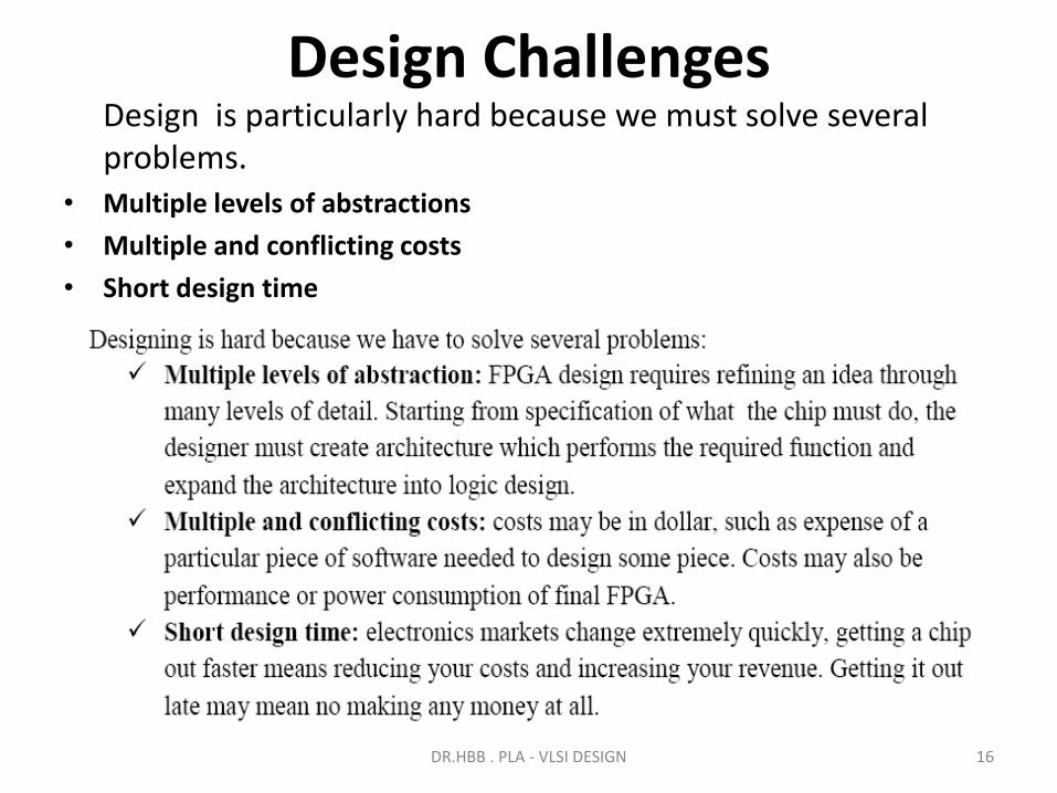
Design ChallengesDesign is particularly hard because we must solve several problems.
• Multiple levels of abstractions
• Multiple and conflicting costs
• Short design time
DR.HBB . PLA - VLSI DESIGN 16
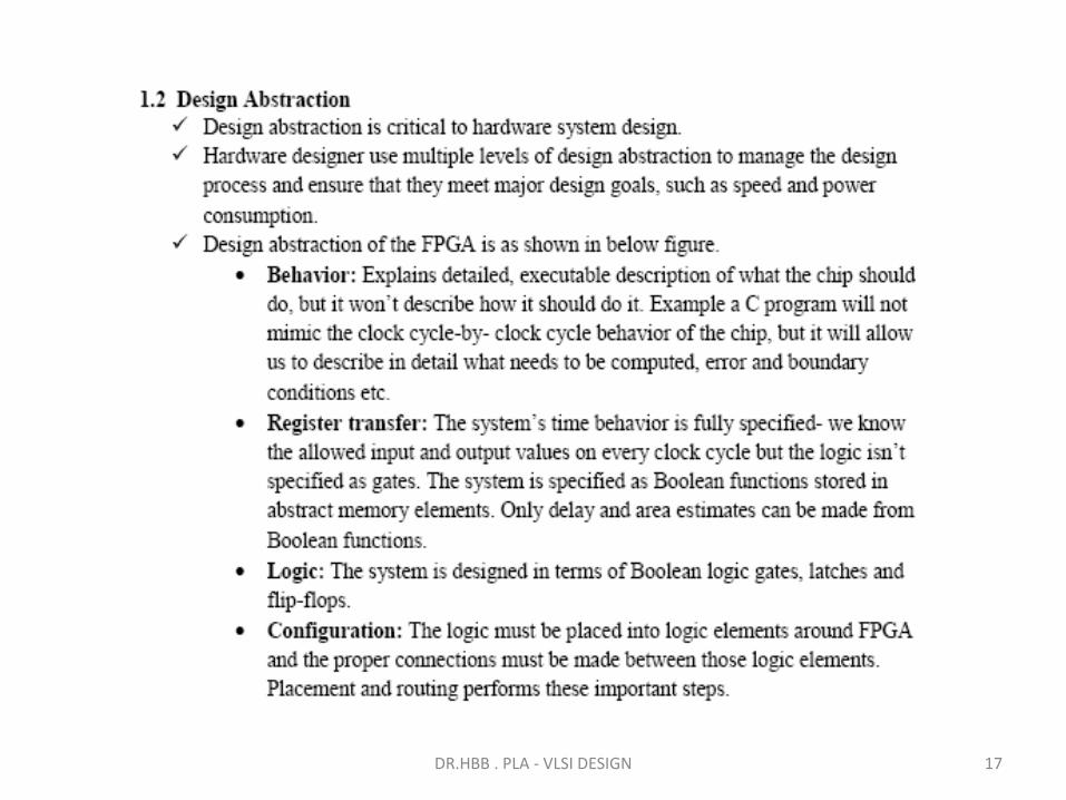
DR.HBB . PLA - VLSI DESIGN 17
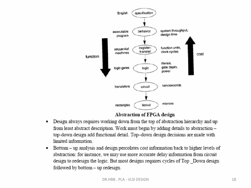
DR.HBB . PLA - VLSI DESIGN 18
Assignments:
Section 1.4.2 ( page 31,32 )
1.4.4 (37,38,39)
DR.HBB . PLA - VLSI DESIGN 19
DR.HBB . PLA - VLSI DESIGN 20
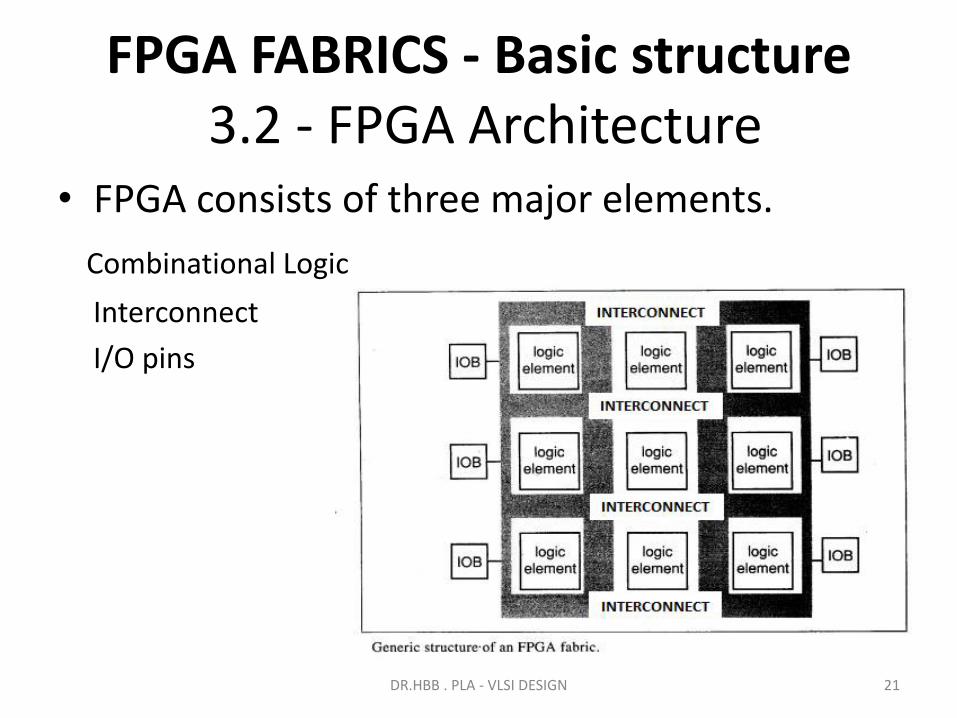
FPGA FABRICS - Basic structure3.2 - FPGA Architecture
• FPGA consists of three major elements.
Combinational Logic
Interconnect
I/O pins
DR.HBB . PLA - VLSI DESIGN 21
DR.HBB . PLA - VLSI DESIGN 22
DR.HBB . PLA - VLSI DESIGN 23
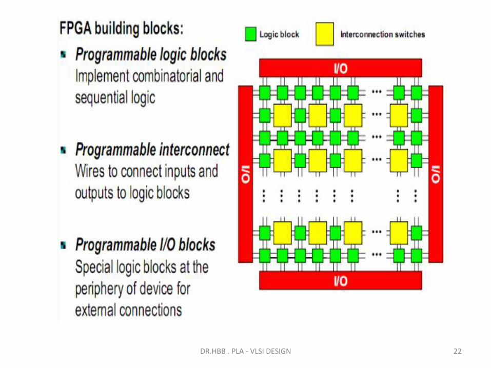
➢The combinational logic is divided into small units which is known as logic
elements(LE) or combinational logic blocks(CLB).
➢ LE or CLB usually forms the functions of several logic gates.
➢Interconnections between these logic elements are made using programmable
interconnects.
➢This interconnects are logically organized into channels or other units.
➢FPGA offers several interconnects depending on the distance between CLB’s that
are to be connected: clock signals are provided with their own interconnection
networks.
➢I/O pins are referred as I/O blocks (IOB’s).
➢These are generally programmable for inputs or outputs and often provides other
features such as low power or high speed connection.
FPGA Architecture
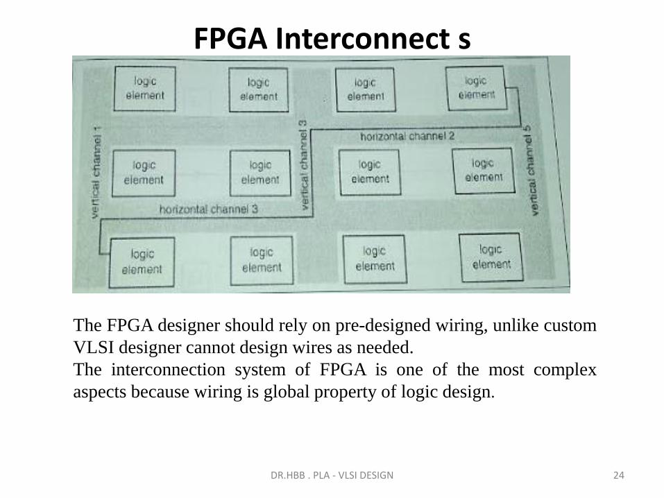
FPGA Interconnect s
DR.HBB . PLA - VLSI DESIGN 24
The FPGA designer should rely on pre-designed wiring, unlike custom
VLSI designer cannot design wires as needed.
The interconnection system of FPGA is one of the most complex
aspects because wiring is global property of logic design.
Connection Paths
• Connection between logic elements requires complex paths since LE’s are
arranged in two dimensional structure as shown in below in previous slide.
• We therefore need to make connections not just between LEs and wires but
also between the wire themselves.
• Wires are typically organized in wiring channels or routing channels
which runs horizontally and vertically throughout the chip.
• Each channel contains several wires ; human designer or program chooses
which wire will carry signal in each channel.
• Connection must be made between wires to carry signal from one point to
another.
• Ex: Net in figure starts from output of LE in upper-right-hand corner
travels down vertical channel 5 until it reaches horizontal channel 2, then
moves down vertical channel 3 to horizontal channel 3, then it uses
vertical channel 1 to reach the input of LE at Lower-left-corner.
DR.HBB . PLA - VLSI DESIGN 25
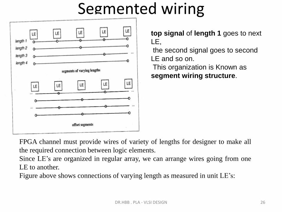
Segmented wiring
DR.HBB . PLA - VLSI DESIGN 26
FPGA channel must provide wires of variety of lengths for designer to make all
the required connection between logic elements.
Since LE’s are organized in regular array, we can arrange wires going from one
LE to another.
Figure above shows connections of varying length as measured in unit LE’s:
top signal of length 1 goes to next
LE,
the second signal goes to second
LE and so on.
This organization is Known as
segment wiring structure.
FPGA Configuration.• All FPGA’s need to be programmed or configured.
• Three major circuit technologies for configuring an FPGA:
a) SRAM
b) Antifuse
c) flash.
• No matter which circuits we use, all the major elements of FPGA - Logic elements, interconnect
and i/O pins needs to be confugured.
DR.HBB . PLA - VLSI DESIGN 27
4.8 Physical Design of FPGA
Configuring an FPGA means placing the logic into LE in fabric and choose
paths .Delay and Energy consumption of LE plays a major role.Physical design is divided into two major phases.
• Placement: it determines the position of logic elements and I/O pads.
• Routing: selects the paths for connection between logic elements and I/O
pads. • These two phases interact – one placement of the logic may not be
routable whereas a different placement of the same logic can be routed. But this division allows us to make physical design problem for tractable.
• We use several different metrics to judge the quality of a Placement or Routing.
DR.HBB . PLA - VLSI DESIGN 28
• Size matters as we are concerned about whether we can fit complete design on to the chip.
• In FPGA, size is closely tied with routing.The number of logic elements required is determined by logic synthesis. If we cannot find legal routing for given placement, we may need to change placement.
• Delay is also critical measure in most design. A long delay is not critical, whereas a relatively short delay path that is critical must be carefully considered.
• Detailed delay characteristics are somewhat expensive to calculate, so tools are used for the same.
DR.HBB . PLA - VLSI DESIGN 29
Placement • The separation of placement and routing raises an important
problem: how to judge the quality of placement?
• We cannot judge the placement quality by 2 measures ( areaand delay).
• We cannot afford to execute a complete routing for everyplacement to judge its quality:
• There fore, we need some metric which estimates the qualityof routing.
• Different algorithms use different metrics, but few simplemetrics suggests important properties of placementalgorithms.
DR.HBB . PLA - VLSI DESIGN 30
DR.HBB . PLA - VLSI DESIGN 31
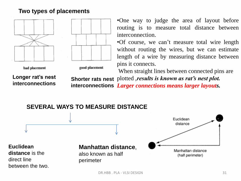
•One way to judge the area of layout before
routing is to measure total distance between
interconnection.
•Of course, we can’t measure total wire length
without routing the wires, but we can estimate
length of a wire by measuring distance between
pins it connects.
When straight lines between connected pins are
plotted ,results is known as rat’s nest plot.
Larger connections means larger layouts.
Two types of placements
Longer rat’s nest
interconnections Shorter rats nest
interconnections
SEVERAL WAYS TO MEASURE DISTANCE
Euclidean
distance is the
direct line
between the two.
Manhattan distance, also known as half
perimeter
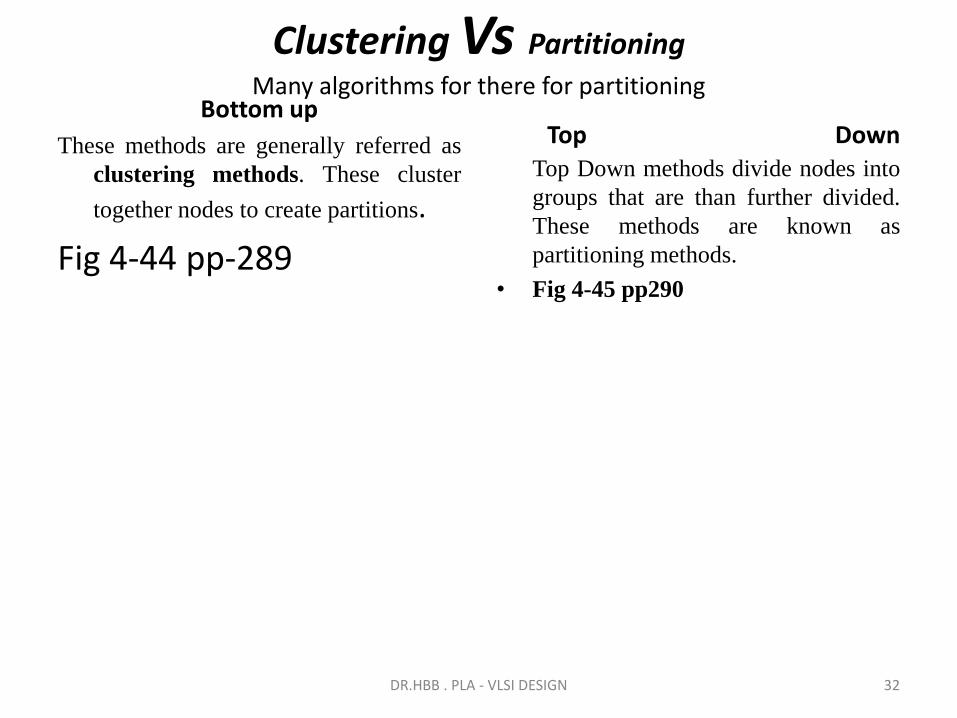
Clustering Vs Partitioning
Many algorithms for there for partitioningBottom up
These methods are generally referred as
clustering methods. These cluster
together nodes to create partitions.
Fig 4-44 pp-289
Top DownTop Down methods divide nodes into
groups that are than further divided.
These methods are known as
partitioning methods.
• Fig 4-45 pp290
DR.HBB . PLA - VLSI DESIGN 32
Placement by clustering .
• Page 292 second pyara
DR.HBB . PLA - VLSI DESIGN 33
Placement by partitioningPartitioning process for mini cut bisecting
criterion is as shown.
Here nodes are components & edges areconnections b/w components.
Goal : to separate the graph nodes into 2partition with nearly equal nodes withminimum edges.
In fig ,we can see 5 wires crossing partitionboundary.
When we swapping ,2 nodes reduces the netcut count to one. Thus a significantreduction.
• 4-46 pp291
DR.HBB . PLA - VLSI DESIGN 34
Routing• Routing selects paths for connections that must be made
between logic elements and I/O pads.
• In an FPGA, the interconnection resources are predeterminedby the architecture of the FPGA fabric.
• A connection must be made by finding sequence of routingresources, all of which unused and which share connectionssuch that continuous path can be made from source to sink.
Routing is generally divided into two phases:
• Global Routing selects general path through the chip but does not determine exact wire segments to be used.
• Detailed Routing selects the exact set of wires to be used for each connections.
DR.HBB . PLA - VLSI DESIGN 35
Costs in routingRouting has two major cost metrics:
wire length
Delay.
Wire length approximates utilization of routing resources. Wemay not use more routing resorces for wires and
Delay may be measured by looking at the delay on paths withlargest number of levels of logic
or
by looking to nets whose delay is close to maximum allowedvalue .
DR.HBB . PLA - VLSI DESIGN 36
Global routing • The principal job during global routing of FPGAs is to balance the
requirements of various nets.
• Nets are routed one at a time, so the order in which nets are routed affects
final result.
• Net may have one of the two problems:
1) it may not be routable because there is no room available to
make connection or
2) it may take a path that incurs too much delay.
• These problems are harder to solve in FPGAs than in custom chip designs
because routing resources are pre determined .
• Connections must be composed of re-designed paths that may include
larger wire segments.
• Most FPGA have diff categories of wiring ,each with very diff CH .
DR.HBB . PLA - VLSI DESIGN 37
Wire ordering
• Many ways have developed to determine the orderin which wires are routed.
• A good heuristic for initial ordering is to route mostdelay critical nets first:
• one may also want to start with large fanout netssince they consume many routing resources.
• In general , a wire may be routed more than oncebefore it finds its final route. Ripup and reroute isone simple strategy for choosing the order in which
to route nets.
DR.HBB . PLA - VLSI DESIGN 38


