Embed Size (px)
Citation preview

New approach for structuralcharacterization of planar sets ofnanoparticles embedded into a solidmatrixDario F. Sanchez1*, Gabriel Marmitt1, Cristiane Marin1, Daniel L. Baptista1, Gustavo de M. Azevedo1,Pedro L. Grande1{ & Paulo F. P. Fichtner1,2
1Instituto de Fısica, Universidade Federal do Rio Grande do Sul (IF-UFRGS), Brazil, 2Department of Metallurgy, Engineering SchoolUFRGS, Brazil.
In this work we demonstrate that Medium Energy Ion Scattering (MEIS) measurements in combinationwith Transmission Electron Microscopy (TEM) or Grazing Incidence Small Angle X-Ray Scattering(GISAXS) can provide a complete characterization of nanoparticle (NP) systems embedded into dielectricfilms. This includes the determination of the nanoparticle characteristics (location, size distribution andnumber concentration) as well as the depth distribution and concentration of the NP atomic componentsdispersed in the matrix. Our studies are performed considering a model case system consisting of planararrangements of Au NPs (size range from 1 to 10 nm) containing three distinct Au concentrationsembedded in a SiO2 film.
The physical properties of metallic nanoparticle (NP) systems embedded in dielectric substrates depend notonly on the NP parameters (location, size distribution and number concentration) but also on the quality ofthe dielectric matrix around the NPs. This applies for photonic devices1 and most particularly for the
development of nonvolatile, high areal number density and low power memory devices2–4. Degraded dielectricsallow trap-to-trap tunneling processes reducing the charge accumulated in the NPs, while high quality dielectricsimprove the memory window, its write/erase speed and its retention and endurance properties5,6. The impuritycontent of a dielectric matrix is a critical degradation issue. The NPs system itself can be regarded as one majorsource of matrix impurities. The NPs are thermodynamically unstable and lead to the formation of a soluteconcentration field of their constituent atoms dissolved within the surrounding matrix as provided, for example,by the Gibbs-Thomson effect7. For Ge NPs in silica, empirical evidence shows that a significantly high fraction ofthe total Ge content in the sample (from 20 to 70%) may remain dissolved in the matrix even after hightemperature thermal treatments8–10. In this case it is argued that, since Ge and Si behave similarly with respectto the formation of tetrahedral bonding structures, Ge atoms could indeed replace Si ones in the SiO2 lattice andtherefore present a high solubility limit. In contrast, for other elements with distinct chemical properties, it isgenerally expected a rather low solubility limit. However, for NP systems produced under non thermodynamic-equilibrium conditions, solute concentrations are difficult to predict and may achieve sufficiently high valuestreading the quality of the surrounding dielectric matrix. Hence, it seems worthwhile to develop reliable tech-niques and methodologies to investigate and characterize NP systems embedded in a solid matrix, not onlydetermining their microstructure properties (size distribution, shape and space arrangement) but also the char-acteristics of the corresponding solute field.
In the present contribution we demonstrate that Medium Energy Ion Scattering (MEIS) measurements andRutherford Backscattering Spectrometry (RBS), in combination with pertinent data from Transmission ElectronMicroscopy (TEM) and/or Grazing Incidence Small Angle X-ray Scattering (GISAXS) can indeed provide arather complete and accurate characterization of buried NP systems. Our studies are performed considering amodel case system consisting of planar arrangements of Au NPs containing three distinct Au concentrationsembedded in a SiO2 film.
GISAXS and TEM are well-established techniques to investigate microstructural properties of such NPsystems11,12. Only recently, the potential of MEIS as a tool for the characterization of shape, sizes, local composition
OPEN
SUBJECT AREAS:CHARACTERIZATION
AND ANALYTICALTECHNIQUES
STRUCTURAL PROPERTIES
NANOPARTICLES
TRANSMISSION ELECTRONMICROSCOPY
Received11 September 2013
Accepted15 November 2013
Published4 December 2013
Correspondence andrequests for materials
should be addressed toD.F.S. (Dario.
*Current address:LETI/DTSI/SCMC,
Commissariat al’energie atomique,Grenoble, France.
{Current address:Department of
Electronic MaterialsEngineering,
Australian NationalUniversity, Canberra,
Australia.
SCIENTIFIC REPORTS | 3 : 3414 | DOI: 10.1038/srep03414 1

and stoichiometry of NPs systems has been more systematicallyexplored, but mostly for surface located nanostructures13–16. For morecomplex systems the MEIS potentialities can be significantlyenhanced with the aid of simulation codes such as thePowerMEIS17,18. This code also accounts for multiple scatteringeffects, which otherwise tend to blur the information extracted fromburied NP systems19. In the present contribution we demonstratethat, it is possible to obtain detailed information not only on themicrostructure properties of the Au NPs but also on the dissolvedpart of the Au content (atomically or as small clusters with a few tensof atoms), which was quantified according to their concentration andthe depth distribution.
ResultsFigure 1a shows a cross-section sketch to illustrate the samples lay-out. Figures 1b–e presents cross-sectional and plan-view TEMmicrographs obtained from samples deposited during 25 and100 s. Planar sets of Au NPs, apparently of the Volmer–Webertype20, are observed for all cases including the 50 s deposited sample(not shown). The plan view micrographs directly allows the deter-mination of the NPs areal densities corresponding to: (13 6 1) 3
1011 NP cm22 for the 25 s deposition case, (11 6 1) 3 1011 NPs cm22
for the 50 s case and (15.3 6 0.5) 3 1011 NPs cm22 for the 100 s case.
Figure 2 shows the size distribution of the NPs as obtained by TEMobservations and GISAXS measurements. For 25 and 50 s, the part-icles are quite spherical-like and their size evaluation is straightfor-ward. For the 100 s case, the particles are rather oblate. Hence,accurate characteristic sizes could not be directly deduced from theGISAXS measurements. From the TEM micrographs, however, theywere estimated by the average from the largest and smaller diameters.We notice that the results from the TEM observations present largermean sizes and variances as compared to the corresponding onesevaluated from the GIXAXS measurements. These differences maybe attributed to the distinct sampling conditions from each tech-nique. For TEM, typically about 300 particles were counted from avery small region of the sample while GISAXS probes a sample areaabout 108 times higher. In addition, to enhance the contrast, TEMimages of small particles are usually taken in out-of-focus conditionswhich tend to artificially enlarge the particle sizes21.
The total amount of the deposited Au measured by MEIS (andconfirmed by RBS measurements) for the 25, 50 and 100 s samplesare 1.8, 3.1 and 7.4 3 1015 Au atoms/cm2, respectively. Taking intoaccount the total amount of deposited Au, MEIS simulations werecarried out using the PowerMEIS code22. An analysis without con-sidering the TEM data could lead to unrealistic results since there aremany free parameters in the simulation. Therefore the NP sizes andnumber concentration obtained by TEM were used as an input to thesimulations18. In order to simulate a MEIS spectrum one has toassume a particular geometrical shape, atomic composition and den-sity. In the present case we assumed 2D arrays of spherical NPs withgiven radius and areal density. Since the total amount of atoms isfixed, only the NP radius was adjusted.
The simulated spectra are then compared with the measured ones asillustrated in Figure 3. This figure shows the ion scattering intensitymaps as a function of ions scattering angle and energy for the threemeasured samples. The columns representing the measured and cal-culated spectra are labeled ‘‘experimental’’ and ‘‘simulation’’. Best fitsare determined by the minimum of the reliability function R2 that reads
R2~1N
XN
i~1
ISim,i{IExp,i� �2
: ð1Þ
Here, ISim and IExp correspond to the simulated and measured ionscattering intensities for scattered angles ranging from 108u to 132uand for scattered energies ranging from 105 to 127 keV. The angle andenergy ranges were chosen in order to cover exclusively the Au signal.The calculated spectra in Figure 3 correspond to the best fit obtained bythe R2 criteria.
Figures 4a to 4c show how the reliability function R2 varies with theNPs radius. The full circles correspond to simulations and the linesare parabolic fittings. The best fit is given by the minimum of thereliability function. The corresponding radius and their uncertaintiesare indicated in each plot.
Figure 4d shows a comparison of radius determined by the para-bolic fit obtained from the MEIS analysis assuming that all Au atomsare contained in the NPs and the NPs size distributions provided byTEM and GISAXS. For the 25 and 50 s cases, the TEM and GISAXSresults are consistent with each other and significantly disagree withthe results from the MEIS analysis. Unlike GISAXS and TEM, theMEIS probe is sensitive to all Au atoms, regardless if they are con-tained in NPs or dispersed in the matrix. Hence, for a number densityof NPs consistent with the one determined from the plan-view TEMmicrographs (see Figure 1), this disagreement indicates that part ofthe deposited Au content is indeed not contained in TEM or GISAXSdetectable NPs, but rather dissolved in the matrix.
In addition, by taking into account the NPs’ size distributions ofthe samples from GISAXS analysis (Figure 2d and 2e), the totalamount of Au detected by MEIS and RBS and the NPs numberdensities from plan-view TEM observations, we can state that only
Figure 1 | (a) Schematic cross-sectional illustration of the samples. TEM
micrographs present cross-section (b, c) and plan-view (d, e) images of the
samples prepared with 25 and 100 s, respectively (diffraction contrast
bright field imaging conditions, underfocus).
www.nature.com/scientificreports
SCIENTIFIC REPORTS | 3 : 3414 | DOI: 10.1038/srep03414 2

a small amount of the Au atoms (28 6 5% for the 25 s sample and 396 9% for the 50 s sample) is actually contained in the NPs. Theseresults are summarized on Table 1. The table also includes the resultsobtained for the 100 s deposited sample, evaluated considering thesize distribution from TEM measurements. For this case we noticethat the NPs’ mean size obtained by MEIS analysis is slightly largerthan the one by TEM, with overlapping uncertainty bars.
The large differences between GISAXS and TEM as compared tothe MEIS results can be attributed to the fact that the samples wereprepared in conditions away from the thermodynamic equilibriumand therefore a significant fraction of Au atoms have not beenincorporated into the particles during the deposition process23.Furthermore, during the deposition of the SiO2 cap layer, it is alsopossible that additional Au atoms may be re-dispersed from theparticles into the silica over layer.
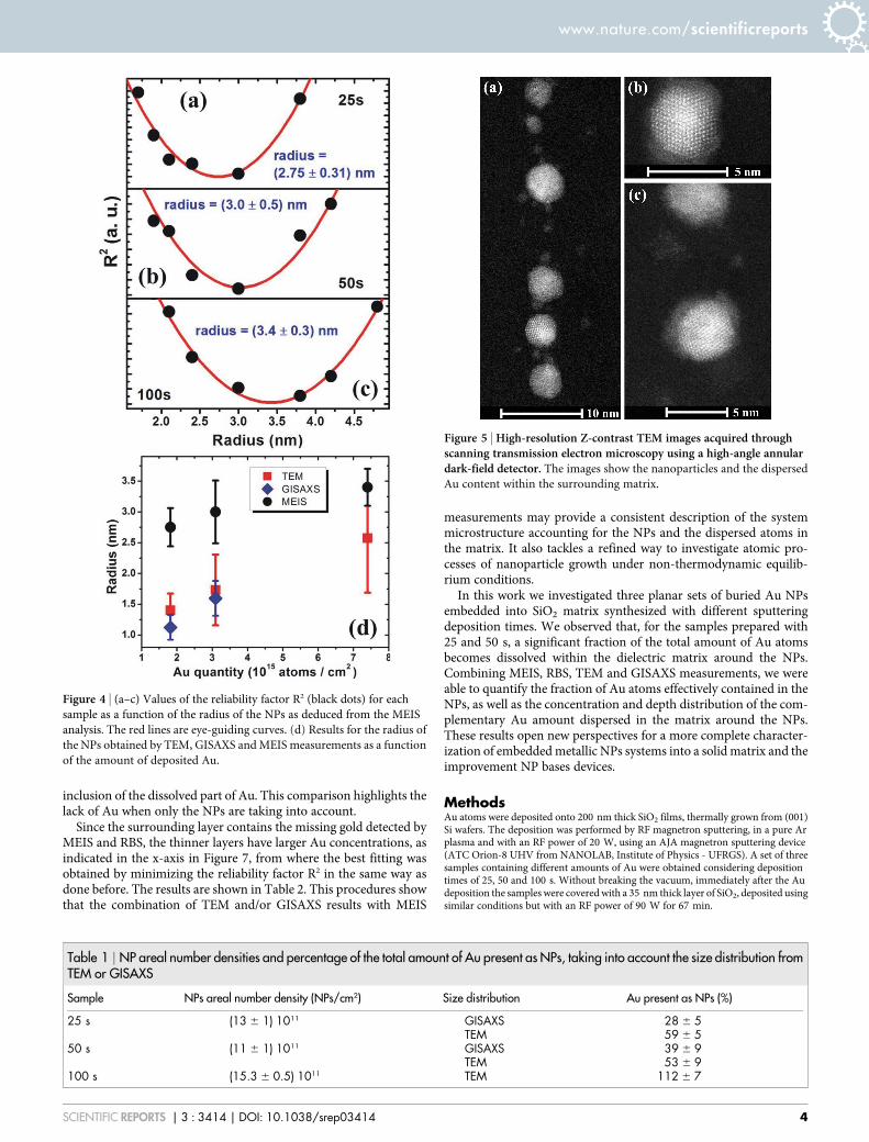
Figure 5 shows TEM micrographs presenting high-resolutionannular dark field Z-contrast images from selected particles and theirsurroundings. The white areas represent the accumulation of Auatoms, which can be detected not only in the NPs but also distributedin the silica matrix surrounding the NPs. These observations are notquantitative but provide a direct evidence of the presence of dis-persed Au atoms and subnanometric clusters as suggested by theMEIS measurements.
DiscussionHence, in order to refine the system characterization, additionalMEIS simulations were then performed accounting for the dissolvedAu content for the 25 and 50 s sample cases. The basic idea of thesimulation concept is illustrated in Figure 5a. It introduces a matrixlayer with thickness h and composition (SiO2)xAu12x, between thethermally grown and the deposited SiO2. Figure 6b to 6g shows thecorresponding MEIS simulations compared to the experimentalscattered intensity profiles for three different scattered angles(109u, 120u and 131u). Two different simulations were performed:1) with (dashed blue line) and 2) without (continuous red line) the
Figure 2 | Particle Size Distributions obtained by TEM (a–c) and GISAXS (d–e) measurements. The corresponding mean radius r and FWHM are also
indicated.
Figure 3 | Experimental and simulated two-dimensional map of ionscattering intensities (2D-MEIS spectra) for the 25, 50 and 100 sdeposited samples taken with 150 keV He1 ions.
www.nature.com/scientificreports
SCIENTIFIC REPORTS | 3 : 3414 | DOI: 10.1038/srep03414 3
inclusion of the dissolved part of Au. This comparison highlights thelack of Au when only the NPs are taking into account.
Since the surrounding layer contains the missing gold detected byMEIS and RBS, the thinner layers have larger Au concentrations, asindicated in the x-axis in Figure 7, from where the best fitting wasobtained by minimizing the reliability factor R2 in the same way asdone before. The results are shown in Table 2. This procedures showthat the combination of TEM and/or GISAXS results with MEIS
measurements may provide a consistent description of the systemmicrostructure accounting for the NPs and the dispersed atoms inthe matrix. It also tackles a refined way to investigate atomic pro-cesses of nanoparticle growth under non-thermodynamic equilib-rium conditions.
In this work we investigated three planar sets of buried Au NPsembedded into SiO2 matrix synthesized with different sputteringdeposition times. We observed that, for the samples prepared with25 and 50 s, a significant fraction of the total amount of Au atomsbecomes dissolved within the dielectric matrix around the NPs.Combining MEIS, RBS, TEM and GISAXS measurements, we wereable to quantify the fraction of Au atoms effectively contained in theNPs, as well as the concentration and depth distribution of the com-plementary Au amount dispersed in the matrix around the NPs.These results open new perspectives for a more complete character-ization of embedded metallic NPs systems into a solid matrix and theimprovement NP bases devices.
MethodsAu atoms were deposited onto 200 nm thick SiO2 films, thermally grown from (001)Si wafers. The deposition was performed by RF magnetron sputtering, in a pure Arplasma and with an RF power of 20 W, using an AJA magnetron sputtering device(ATC Orion-8 UHV from NANOLAB, Institute of Physics - UFRGS). A set of threesamples containing different amounts of Au were obtained considering depositiontimes of 25, 50 and 100 s. Without breaking the vacuum, immediately after the Audeposition the samples were covered with a 35 nm thick layer of SiO2, deposited usingsimilar conditions but with an RF power of 90 W for 67 min.
Table 1 | NP areal number densities and percentage of the total amount of Au present as NPs, taking into account the size distribution fromTEM or GISAXS
Sample NPs areal number density (NPs/cm2) Size distribution Au present as NPs (%)
25 s (13 6 1) 1011 GISAXS 28 6 5TEM 59 6 5
50 s (11 6 1) 1011 GISAXS 39 6 9TEM 53 6 9
100 s (15.3 6 0.5) 1011 TEM 112 6 7
Figure 4 | (a–c) Values of the reliability factor R2 (black dots) for eachsample as a function of the radius of the NPs as deduced from the MEISanalysis. The red lines are eye-guiding curves. (d) Results for the radius of
the NPs obtained by TEM, GISAXS and MEIS measurements as a function
of the amount of deposited Au.
Figure 5 | High-resolution Z-contrast TEM images acquired throughscanning transmission electron microscopy using a high-angle annulardark-field detector. The images show the nanoparticles and the dispersed
Au content within the surrounding matrix.
www.nature.com/scientificreports
SCIENTIFIC REPORTS | 3 : 3414 | DOI: 10.1038/srep03414 4

These samples were then directly investigated by MEIS, RBS, TEM and GISAXS.The MEIS measurements were performed using a 150 keV He1 ion beam. Thesamples were mounted in a 3-axis goniometer inside the analysis chamber kept undera pressure of about 1027 mbar. Typical beam current was less than 15 nA. The angleof incidence used was of 10u and backscattered He1 ions emerging from the targetwere analyzed using a Toroidal Electrostatic Analyzer (TEA) mounted at 120 degreeswith respect to the beam direction. At the top end of the TEA a set of two micro-channel plates coupled to a position-sensitive detector allows each ion to be energy-and angle-analyzed leading to 2-D spectra. The TEA angular aperture is 24 degreesand each angle bin corresponds to 0.08 degrees. The overall energy resolution of thesystem is 600 eV. Details of the data analysis are described in refs. 17–19, 22. TheMEIS analysis was performed using the 500 kV electrostatic accelerator from the IonImplantation Laboratory (LII), IF–UFRGS. The MEIS measurements were analyzedusing the PowerMEIS package22 where the sample is discretized layer by layer usingfull 3D matrices. Each one represents a layer, and each element of the matrix standsfor specific composition, stoichiometry and density of the material. In this way the setof NPs was generated with specific shapes, size and pair correlation function. ThePowerMEIS program can handle any geometric shape, size distribution, and densityof the nanostructures. It also accounts for the asymmetry of the energy loss-distri-bution due to the backscattering collision and to multiple scattering effects.
Standard Rutherford backscattering Spectrometry (RBS) experiments were alsoperformed using a 1.4 MeV He21 ion beam from the 3 MV tandetrom acceleratorfrom the LII-IF-UFRGS.
TEM observations were performed in cross-sectional and plan-view samplesprepared by ion milling. The samples were characterized at 200 keV via selected areadiffraction measurements (SAD) as well as via diffraction and phase contrastobservations modes to determine shape, size, size distribution, spatial order and phaseof the NPs using a JEM 2010 microscope from the Center of Electron Microscopy
UFRGS. Additional high-resolution observations were carried out in a Cs-correctedFEI Titan 80/300 microscope from the Brazilian National Institute of Metrology(INMETRO). Z-contrast images were acquired through scanning transmissionelectron microscopy (STEM) using a high-angle annular dark-field detector
Figure 6 | (a) Illustration of the system characteristics considering the planar set of NPs embedded in a matrix containing Au atoms (i.e. (SiO2)xAuy)distributed in a layer with thickness h. (b–g) Results for the 25 and 50 s cases showing the experimental scattered intensities profiles (gray line-circles) as a
function of energy for three scattered angles and the simulated ones. The simulations considering the Au content present only in the NPs are shown in
continuous red lines. Those considering the NPs and the dissolved Au atoms within the surrounding matrix are represented by dashed blue lines.
Figure 7 | The reliability R2 values (black dots) as a function of the Auconcentration in the surrounding layer (SiO2)xAuy, as illustrated inFigure 5. The red lines are eye-guiding curves.
www.nature.com/scientificreports
SCIENTIFIC REPORTS | 3 : 3414 | DOI: 10.1038/srep03414 5

(HAADF). The GISAXS measurements were performed in the Brazilian SynchrotronLight Source LNLS, with 8.5 keV of X-ray energy. The GISAXS data were analyzedwith the FitGISAXS package24 developed within the IGOR Pro analysis software(WaveMetrics, Inc.).
1. Okubo, N., Umeda, N., Takeda, Y. & Kishimoto, N. Enhancement of metal-nanoparticle precipitation by co-irradiation of high-energy heavy ions and laserin silica glass. Nucl. Instr. and Meth. B 206, 610–614 (2003).
2. Tiwari, S. et al. Volatile and non-volatile memories in silicon with nano-crystalstorage. Paper presented at Electron Devices Meeting, Washington, DC. Place ofpublication: IEEE Int. Electron. Devices Meet. Tech. Dig., 521–524 (1995,December).
3. Tiwari, S. et al. A silicon nanocrystals based memory. Appl. Phys. Lett. 68, 1377(1996).
4. Diaz, R., Grisolia, J., Pecassou, B., Shalchian, M. & BenAssayag, G. Functionalnanocrystal-based memories with extraction of nanocrystals properties by chargepumping technique. Solid-State Electron. 82, 11–15 (2013).
5. Chen, W. R. et al. Formation of stacked Ni silicide nanocrystals for nonvolatilememory application. Appl. Phys. Lett. 90, 112108 (2007).
6. Chen, S.-C. et al. Nonvolatile memory effect of tungsten nanocrystals underoxygen plasma treatments. Thin Solid Films 518, 7339–7342 (2010).
7. Porter, D. & Easterling, K. E. Phase transformations in metals and alloys(Chapman & Hall, London, 1992).
8. Lopes, J. M. J. et al. Cluster coarsening and luminescence emission intensity of Genanoclusters in SiO2 layers. J. Appl. Phys. 94, 6059 (2003).
9. Sahoo, P. K., Gasiorek, S. & Lieb, K. P. Cathodoluminescence and epitaxy aftersequential Rb- and Ge-ion implantation in a-quartz. Nucl. Instr. and Meth. inPhys. Res. B 240, 188–193 (2005).
10. Gasperini, A. et al. Investigation of indirect structural and chemical parameters ofGeSi nanoparticles in a silica matrix by combined synchrotron radiationtechniques. J. Appl. Cryst. 45, 71–84 (2012).
11. Renaud, G., Lazzari, R. & Leroy, F. Probing surface and interface morphology withgrazing incidence small angle X-ray scattering. Surf. Sci. Rep. 64, 255–380 (2009).
12. Biasiol, G. & Heun, S. Compositional mapping of semiconductor quantum dotsand rings. Phys. Rep. 500, 117–173 (2011).
13. Konomi, I., Hyodo, S. & Motohiro, T. Simulation of MEIS spectra for quantitativeunderstanding of average size, composition, and size distribution of Pt–Rh alloynanoparticles. J. Catal. 192, 11 (2000).
14. Okazawa, T., Kohyama, M. & Kido, Y. Electronic properties of Au nanoparticlessupported on stoichiometric and reduced TiO2(110) substrates. Surf. Sci. 600,4430 (2006).
15. Quinn, P. D. et al. Composition profiles of InAs–GaAs quantum dots determinedby medium-energy ion scattering. Appl. Phys. Lett. 87, 153110 (2005).
16. Matsumoto, H. et al. Au(core)/Pd(shell) structures analyzed by high-resolutionmedium energy ion scattering. Nucl. Instrum. Methods Phys. Res. Sect. B 268, 2281(2010).
17. Sortica, M. A. et al. Structural characterization of CdSe/ZnS quantum dots usingmedium energy ion scattering. Appl. Phys. Lett. 101, 023110 (2012).
18. Leveneur, J. et al. Iron-based bimagnetic core/shell nanostructures in SiO2: a TEM,MEIS, and energy-resolved XPS analysis. J. Nanopart. Res. 14, 1149 (2012).
19. Sanchez, D. F. et al. Structural characterization of Pb nanoislands in SiO2/Siinterface synthesized by ion implantation through MEIS analysis. Surf. Sci. 605,654–658 (2011).
20. Ruffino, F., Giannazzo, F., Roccaforte, F., Raineri, V. & Grimaldi, M. G. TowardFunctional Nanomaterials [Wang, Z. M. (ed.)] [127–171] (Springer, New York,2009).
21. Jenkins, M. L. & Kirk, M. A. Characterization of Radiation Damage byTransmission Electron Microscopy, (IOP Publishing Ltd, London, 2001).
22. Sortica, M. A., Grande, P. L., Machado, G. & Miotti, L. Characterization ofnanoparticles through medium-energy ion scattering. J. Appl. Phys. 106, 114320(2009).
23. Ruffino, F. et al. Self-organization of gold nanoclusters on hexagonal SiC and SiO2
surfaces. J. Appl. Phys. 101, 064306 (2007).24. Babonneau, D. FitGISAXS: software package for modelling and analysis of
GISAXS data using IGOR Pro. J. Appl. Cryst. 43, 929–936 (2010).
AcknowledgmentsThe authors acknowledge the financial support by brazilian agencies CNPq, FAPERGS,PRONEX program, the use of the infrastructure of Center for Electron Microscopy and theIon Beam Implantation Laboratory at UFRGS and of the facilities from the BrazilianNational Institute of Metrology and the Brazilian Synchrotron Light Laboratory (XRD2beam line).
Author contributionsG.M. worked on the modification of the PowerMEIS source code by including MultipleScattering effects, which is important for buried nanostructures in solid matrix. C.M.worked on the sample synthesis and GISAXS experiments. D.L.B. measured and analyzedby STEM-HAADF and prepared the figure 6. G.M.A. worked on the GISAXS experimentsand analysis. P.L.G. worked on the MEIS experiments and analysis. P.F.P.F. worked on theTEM experiments and analysis. D.F.S. wrote the main manuscript text, prepared the figures,planed and worked on the MEIS, GISAXS and TEM experiments and analysis, planed andworked on the sample synthesis and prepared all the samples for TEM and STEM-HAADFexperiments. All authors reviewed the manuscript.
Additional informationCompeting financial interests: The authors declare no competing financial interests.
How to cite this article: Sanchez, D.F. et al. New approach for structural characterization ofplanar sets of nanoparticles embedded into a solid matrix. Sci. Rep. 3, 3414; DOI:10.1038/srep03414 (2013).
This work is licensed under a Creative Commons Attribution-NonCommercial-NoDerivs 3.0 Unported license. To view a copy of this license,
visit http://creativecommons.org/licenses/by-nc-nd/3.0
Table 2 | The surrounding layer thickness h and the correspondingAu concentration, both obtained from the minimum value of R2 fromFigure 7
Sample Surrounding layer thickness h (nm) Au concentration (at.%)
25 s 4.0 6 0.3 5.1 6 0.450 s 5.1 6 0.7 6.0 6 0.9
www.nature.com/scientificreports
SCIENTIFIC REPORTS | 3 : 3414 | DOI: 10.1038/srep03414 6


