Embed Size (px)
Citation preview

IEEE TRANSACTIONS ON TERAHERTZ SCIENCE AND TECHNOLOGY, VOL. 5, NO. 6, NOVEMBER 2015 941
Nonlocal Effects on Surface Plasmon PolaritonPropagation in Graphene Nanoribbons
Giampiero Lovat, Member, IEEE, Rodolfo Araneo, Senior Member, IEEE, Paolo Burghignoli, Senior Member, IEEE,and George W. Hanson, Fellow, IEEE
Abstract—Fundamental properties of surface plasmon polaritonmodes propagating along graphene nanoribbons are investigatedby means of a full-wave method-of-moments approach adoptinga spatially dispersive dyadic model for graphene conductivity.Modal propagation, current profiles, field distributions, and char-acteristic impedances are studied in detail showing the dramaticeffects of spatial dispersion and the need to go beyond the usualweak (low- ) spatial dispersion formulation.Index Terms—Graphene, nanoribbons, surface plasmon
polariton.
I. INTRODUCTION
P LANAR electromagnetic structures incorporatinggraphene layers have received considerable attention
in the last few years for waveguide, antenna, and shieldingapplications. In particular, graphene nanoribbons (GNRs) havebeen proposed in various configurations, as possible intercon-nects in integrated circuits [1]–[3]. GNRs, either free-standingor placed in a stratified dielectric structure, support a varietyof propagation modes, including surface-plasmon modes [4],[5]. Surface plasmon polariton (SPP) propagation in graphenenanostructures has recently attracted interest for the possibilityof strong confinement of electromagnetic energy at subwave-length scales, tuned and controlled by a gate voltage or throughchemical doping. Other applications of graphene plasmonsinclude optical signal processing, light modulation, sensing,spectral photometry, quantum optics, and nonlinear photonics[6], [7].Here, we aim at studying the fundamental properties of the
dominant SPP mode supported by a monolayer GNR placedon top of a dielectric substrate, employing a rigorous full-wavenon-Galerkin method-of-moments (MoM) approach in thespectral domain: the non-Galerkin characteristic (i.e., testfunctions different from the basis functions) has been chosento ensure convergence of the spectral integrals defining theMoM matrix. The GNR is modeled through an appropriate
Manuscript received January 14, 2015; revised July 13, 2015; acceptedSeptember 02, 2015. Date of publication October 06, 2015; date of currentversion November 23, 2015. (Corresponding author: Giampiero Lovat.)G. Lovat and R. Araneo are with DIAEE, University of Rome “Sapienza,”
00184 Rome, Italy (e-mail: [email protected]).P. Burghignoli is with DIET, University of Rome “Sapienza,” 00184 Rome,
Italy.G. W. Hanson is with the Department of Electrical Engineering, University
of Wisconsin-Milwaukee, Milwaukee, WI 53211 USA.Color versions of one or more of the figures in this paper are available online
at http://ieeexplore.ieee.org.Digital Object Identifier 10.1109/TTHZ.2015.2477600
tensor surface-impedance boundary condition which takes intoaccount the possible presence of static bias fields and alsoincludes spatial-dispersion effects: this means that grapheneis represented through a dyadic conductivity whose elementsdepend also on the spectral wavenumbers [8], [9]. It is worthnoting that the effects of spatial dispersion on the electromag-netic properties of different graphene structures have recentlybeen studied mainly in connection with infinite graphene-sheetstructures [10]–[13] and it has been shown that they can dra-matically change device performance. Although many studieshave been devoted to SPP propagation in GNRs [4], [5], [14],to the best of our knowledge, none has fully addressed the issueof nonlocality (a preliminary investigation on nonlocal effectsin GNRs has been presented in [15], but the authors used alow- model that we will show below to be insufficient forcorrect modeling).In the present study, we investigate how spatial dispersion af-
fects the propagation properties along a GNR giving particularattention to the dispersion curves, current profiles, field distri-butions, and characteristic impedances of the fundamental SPPmode.It is worth mentioning that, in the more general framework of
using GNRs in graphene-based devices and circuits, two criticalaspects are SPP excitation and graphene-metal contacts.As concerns the excitation problem, which is a hot research
topic, recent studies demonstrated excitation and detection ofSPPs in graphene through near-field microscopy nanotips [16],[17]; however, the low excitation efficiency of such near-fieldsources has prompted research on alternative approaches basedon free-space electromagnetic waves. In this case the main diffi-culty arises from the large momentum mismatch between plas-mons and incoming waves, but different techniques have al-ready been successfully developed in this connection, e.g., at-tenuated total reflection (ATR), scattering from a topological de-fect at the conductor surface, and Bragg scattering using diffrac-tion gratings or a periodic corrugation of the surface of theconductor [18]–[20]. Although these techniques have been pro-posed in connection with infinite graphene sheets as well as ar-rays of GNRs, they may presumably be considered also for theexcitation of a single GNR.As concerns metal-graphene contacts, these constitute a po-
tential limiting factor, especially in active devices, because ofthe possible occurrence of very large contact resistances, due toseveral physical and technological reasons, e.g., the low densityof states in graphene compared with that of metals, the forma-tion of dipoles and defects at the interface, etc. [21].
2156-342X © 2015 IEEE. Personal use is permitted, but republication/redistribution requires IEEE permission.See http://www.ieee.org/publications_standards/publications/rights/index.html for more information.

942 IEEE TRANSACTIONS ON TERAHERTZ SCIENCE AND TECHNOLOGY, VOL. 5, NO. 6, NOVEMBER 2015
Fig. 1. GNR over a dielectric substrate. Parameters of the reference structure:200 nm and 400 nm.
Both the considered topics, although important, are beyondthe scope of the present investigation.
II. DESCRIPTION OF THE PROBLEMThe electromagnetic problem under analysis is sketched in
Fig. 1. It consists of a graphene sheet of width along the -di-rection (i.e., a GNR) deposited on a a laterally infinite dielectricsubstrate of thickness along the -direction and relative per-mittivity . All of the units are in the SI system and a time-har-monic variation is assumed and suppressed throughout.Propagation along the -direction, i.e., modes with a spatial de-pendence , is also assumed.
A. Graphene ConductivityIn general, a graphene sheet can be modeled as a conductive
sheet with a dyadic surface conductivity [22]
(1)
In the absence of magnetic bias and neglecting spatial disper-sion, graphene can be simply characterized by a scalar localconductivity , which depends on external and internal param-eters, e.g., radian frequency , temperature , a phenomeno-logical scattering rate (where is the relaxation timedepending on a variety of factors and determined experimen-tally), and the chemical potential (which can be controlledeither through doping or through an applied bias electric fieldorthogonal to the graphene plate) [8]. Moreover, for the consid-ered frequency range (i.e., below hundreds of THz), only the in-traband contributions are considered, the interband terms beingnegligible [8]. In this case
(2)
where
(3)
and , thus showing aDrude-like behavior. In (3)–is the electron charge, 10 m/s is the Fermi velocityin graphene, while and are the reduced Planck and theBoltzmann constants, respectively.When amore refinedmodel is considered which takes into ac-
count spatial dispersion, the graphene conductivity has a dyadicform, whose elements have been derived in [8] under a low-
relaxation-time approximation (RTA) and, more recently, in[9] for arbitrary values and with the Bhatnagar–Gross–Krook(BGK) model (which allows for including charge diffusion andderiving the correct quantum capacitance). For completeness,the expressions for the dyadic elements for different grapheneconductivity models are reported in the Appendix.
B. Dispersion AnalysisStarting from the boundary condition
on the GNR surface, the electric fieldintegral equation (EFIE) can be expressed in the form
(4)
for and for any , where is theEJ-type dyadic Green function for planar layered media,
is the Fourier transform of the modal surface current, and is the dyadic resistivity. By introducing
the spectral-domain Green's function and repre-senting the surface current of the mode as
(5)where is the assumed propagation constant, aftersome manipulations, (4) can be rewritten as
(6)for , where is the Fourier transformof the modal surface current .Equation (6) is clearly a nonstandard eigenvalue equation:
it has an infinite number of solutions, each of which identifiesa propagation mode of the nanoribbon through its propagationconstant and its surface current distribution .
C. Numerical SolutionA standard MoM procedure can be used to solve the eigen-
value problem.In particular, by expanding the and components of the
modal current in and entire-domain (e.g., sinusoidal) basisfunctions and , respectively, as
(7a)
(7b)
where and are unknown coefficients and
(8a)
(8b)
LOVAT et al.: NONLOCAL EFFECTS ON SURFACE PLASMON POLARITON PROPAGATION IN GRAPHENE NANORIBBONS 943
It should be observed that the Fourier transforms of the basisfunctions in (8) are
(9a)
(9b)
By applying a non-Galerkin test procedure with test functions( ), (6) can be recast in the following matrix
form:
(10)
where , , and
(11)
where , , , and are the compo-nents of the dyadic resistivity . In particular, suitable test func-tions need to be chosen in order to ensure the convergence of thespectral integral in (11) [23]. This is not trivial, since it can beshown, based on the expressions derived in the Appendix, thatin a full- formulation we have
(12)
Hence, if the classical Galerkin test procedure were used, the in-tegrand functions of the matrix elements would showan asymptotic behavior as without alternating sign thusleading to non-convergent integrals.A suitable choice of test functions is instead
(13a)
(13b)
The Fourier transform of (13a) is the same as in (9a), and it hasan asymptotic behavior as , while the Fourier transformof (13b) is
(14)
with an asymptotic behavior as which ensures the con-vergence of all of the integrals (11).The computation of the matrix elements in (11) involves the
integration of functions which oscillate as : the in-tegration can then efficiently be performed through the doubleexponential formulas proposed in [24].The eigenvalues have to be found searching for the com-
plex zeroes of the determinant of the square matrix in(10), i.e.,
(15)
and a dispersion analysis can easily be performedtracking the relevant complex pole as a function of the fre-quency .Although several method are available for searching zeros on
the complex plane [25], [26], the Müller's method is here em-ployed since it is simple and robust. Since the number of iter-ations required to converge to the correct propagation constant(matrix eigenvalue) strictly depends on the initial guess, asuitable predictor has been developed based on an extrapolationprocedure of the previous ten eigenvalues found at the previousfrequencies. It results in a very efficient code that is able to trackthe eigenvalue at each frequency step with just three or four it-erations.
D. Current, Field, and Characteristic Impedance CalculationOnce the propagation constant that makes null the determi-
nant of the MoM matrix at a prescribed frequency is found, theeigenfunctions associated with the matrix can easily becomputed and the eigenfunction corresponding to the minimumeigenvalue (which is null within the machine accuracy) givesthe expansion coefficients in (7); this way, both the longitudinaland transverse current components can easily be computed.Once the modal current on the GNR surface is
known, the modal field components can then be computed as
(16a)
(16b)
(16c)
where while and are the EJ- andHJ-type spectral-domain dyadic Green's functions, respec-tively [27]. It is worth noting that the computation of all ofthe involved integrals can be made more efficient by suitablyexploiting the symmetries of the integrand functions.The characteristic impedance is then calculated according to
the current-power definition [28]
(17)
where the integral in the numerator of (17) is recursively com-puted over an increasing surface centered on the GNR and trun-cated when the prescribed accuracy is reached.
III. RESULTS
A. Graphene Conductivity and Basic StructureHere, a comparison among the different graphene conduc-
tivity models is presented for different radian frequencies , as-suming in all cases 0.5 ps, 0 eV, and 300 K.The conductivity dyadic will be represented in polar coordi-nates, showing results for the longitudinal and transverse con-ductivities and as functions of the radial wavenumbernormalized with respect to the free-space wavenumber [37].

944 IEEE TRANSACTIONS ON TERAHERTZ SCIENCE AND TECHNOLOGY, VOL. 5, NO. 6, NOVEMBER 2015
Fig. 2. Absolute values of (a) and (b) as functions of at1 THz.
For clarity, we summarize the different models considered. Forthe RTA formulations there are two conductivity expressions:the full- expression and the low- approximation (cf. (33)-(34)and (28)–(29), respectively). For the BGK formulation, whichis more accurate than the RTA, we also have two conductivityexpressions: the full- expression and the low- approximation(cf. (30)-(31) and (26)-(27), respectively). We also show thescalar local model (2). Similar results have already been shownin [9], but we report them here for completeness and then focuson nonlocal GNR modal properties which have not been exam-ined in detail.In Fig. 2, the absolute values of and are shown at
1 THz. For both components, the full- RTA andBGK models are in excellent agreement, whereas the scalarlocal conductivity and both the low- RTA and BGK modelsare accurate only in a low- range, as expected; this range ishowever narrower for than for . In particular, it shouldbe noted that the low- formulations completely fail for large, even more than the local model: this is to be expected sinceboth the low- elements have an asymptotic behavior as
, while the full- longitudinal and transverse elements areand , respectively (the local formulation is
instead independent of , i.e., ).
Fig. 3. Normalized phase ( ) and attenuation ( ) constants as func-tions of frequency for a structure as in Fig. 1 with . Different conduc-tivity models are considered: a local model, a low- BGK model, and a full-BGK model.
In order to show the effects of spatial dispersion on the elec-tromagnetic properties of GNRs, we consider a GNR structurewith 200 nm (more than two orders of magnitude largerthan the graphene lattice constant , so that electronic edge-ef-fects can be ignored) and 400 nm, with different permit-tivity values for the substrate. All of the results have been ob-tained with six basis functions for each current component (i.e.,
) which provide converged results.
B. SPP Propagation Characteristics
In Fig. 3, the dispersion properties of the fundamentalSPP mode supported by a free-standing GNR (i.e., )are reported in a logarithmic scale. In particular, the nor-malized phase ( ) and attenuation( ) constants are plotted as functions offrequency by adopting three different conductivity models forgraphene, i.e., a local formulation, a low- BGK formulation,and a full- BGK formulation. The latter fully takes intoaccount the nonlocal effects which are seen to be particularlypronounced in the lowest (microwave) frequency range. Onthe other hand, as expected, the low- formulation leads toerroneous results especially in the lowest frequency range (thishappens both in the RTA and BGK formulations).In Fig. 4(a) and (b), the normalized phase and attenua-
tion constants are reported as functions of frequency for afree-standing GNR with different ribbon widths: from Fig. 4, itcan thus be seen that nonlocal effects are stronger for ribbonswith narrower widths and negligible for ribbons with widthslarger than 1 m.In Fig. 5(a) and (b), the dispersion properties are reported for
a GNR with two different permittivities of the substrate, i.e., amoderate permittivity [Fig. 5(a)] and a high permit-tivity [Fig. 5(b)]. In these cases the low- results havenot been reported since it can be shown that such a low- formu-lation dramatically fails. On the other hand, it can easily be seenthat increasing the dielectric permittivity strongly enhances thespatial-dispersion effects, as shown in [11] for modes supportedby an infinite graphene sheet. In particular, it can be seen thatin the high-permittivity case ignoring spatial dispersion leads

LOVAT et al.: NONLOCAL EFFECTS ON SURFACE PLASMON POLARITON PROPAGATION IN GRAPHENE NANORIBBONS 945
Fig. 4. Normalized propagation constants as functions of frequency for astructure as in Fig. 1 with for different ribbon widths. Two differentconductivity models are considered, i.e., a local model and a full- BGK modelfor the calculation of (a) the normalized phase constant and (b) the nor-malized attenuation constant .
to relative errors in the calculation of the phase and attenua-tion constants which are both larger than 50% at 10 THz: at lowfrequencies such errors are still larger. In the considered fre-quency range, including spatial dispersion increases the atten-uation constant of the plasmon mode, except for the high-per-mittivity case in the higher part of the frequency spectrum: insuch a case, e.g., at 10 THz, spatial dispersion leads to anattenuation constant much lower than that of the local formula-tion. Instead, as concerns the phase constant, spatial dispersionmakes the plasmon mode much slower at lower frequencies andmuch faster at higher frequencies.
C. Modal Currents and Field DistributionsIn Fig. 6, the amplitude of the longitudinal -component of
the modal current along the nanoribbon (normalized to its max-imum value) is reported at the operating frequency 1 THzfor a structure as in Fig. 3. The transverse -component is notreported since its value is more than three-orders of magnitudesmaller than the longitudinal component . It can be seen thatignoring spatial dispersion or using a spatially-dispersive modelvalid for low wave numbers leads to completely erroneous cur-rent profiles. In particular, the almost constant behavior typical
Fig. 5. Normalized phase ( ) and attenuation ( ) constants as func-tions of frequency for a structure as in Fig. 1 with (a) and (b)
. Two different conductivity models are considered, i.e., a local model anda full- BGK model.
of the fundamental mode in microwave microstrip line is ob-tained using a purely local model, whereas the correct spatiallydispersive full- conductivity formulation determines a variablecurrent profile across the ribbon with a minimum at the edgesand a maximum near the center of the graphene nanostrip. Sucha behavior is exactly the opposite of what is found adopting alow- model which predicts a current profile far from both thepurely local model and the correct spatially dispersive model.Again, using a low- model in such problems dramatically af-fects the correctness of the results.It is worth noting that the behavior shown in Fig. 6 is qualita-
tively the same across the considered frequency spectrum (from10 GHz to 10 THz) and for structures with different substratepermittivities.The normalized electric and magnetic field distributions are
reported in Fig. 7(a) and (b), respectively, for a structure as inFig. 6 (i.e., and 1 THz). They show a classical2-D monopole-like behavior and have been obtained using thefull- conductivity formulation. A local model would lead to thesame qualitative field behavior: to observe the quantitative dif-ferences, in Fig. 8(a) the amplitude of the normalized electricfields are reported as functions of for at 1 THz

946 IEEE TRANSACTIONS ON TERAHERTZ SCIENCE AND TECHNOLOGY, VOL. 5, NO. 6, NOVEMBER 2015
Fig. 6. Normalized -component of the modal current across thenanoribbon for a structure as in Fig. 1 with and 1 THz. Differentconductivity models are considered: a local model, a low- BGK model, anda full- BGK model.
Fig. 7. Normalized (a) electric and (b) magnetic field distribution of theplasmon mode for a structure as in Fig. 6 using a full- BGK model.
for a free-standing GNR. In order to point out the spatial-disper-sion effects in the modal field distributions of GNRs the same ofFig. 8(a) is reported in Fig. 8(b) for a structure withand at 10 THz. It can be seen that, while in the formercase the plasmon mode is poorly confined and spatial-disper-sion effects are negligible, in the latter the electric field is wellconcentrated near the ribbon, although the inclusion of spatialdispersion greatly reduces the amount of field confinement. Thisalso occurs for, e.g., localized surface plasmons, where spatialdispersion reduces the field concentration in the gap betweentwo plasmonic dimers [29].
Fig. 8. Amplitude of the normalized electric field as a function of for a struc-ture as in Fig. 1. Parameters: (a) and 1 THz and (b)and 10 THz.
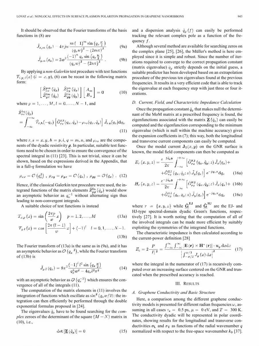
D. Characteristic ImpedanceThe real and imaginary parts of the characteristic impedance
are reported as functions of frequency in Fig. 9(a) for a free-standing GNR as in Figs. 3 and in Figs. 9(b) for a high-dielectricGNR as in Fig. 5(b). As it can be seen, at low frequencies, boththe real and imaginary parts are of the order of k , and there isa significant discrepancy between the local model and the full-BGK formulation: such a discrepancy disappears beyond 1 THzfor the real part and beyond 2 THz the imaginary part becomeone order of magnitude smaller than the real part. Interestingly,the spatial-dispersion effects on the characteristic impedance ofthe GNR are weaker in the high-permittivity case.
E. Electrical Conductivity TuningAs is well known, one of the most attractive characteristic of
graphene is the possibility of externally controlling its electricalconductivity bymodifying the chemical potential : this can beobtained either by applying an electrostatic bias or by doping[8]. In a more general framework, such an external tuning couldbe used to dynamically control the reflection, absorption, orpolarization of the electromagnetic waves impinging against agraphene shield [30], to control the radiation characteristics ofleaky-wave antennas [31], or to make graphene layers workingas tunable cloacks [32]. Moreover, in recent works it has been
LOVAT et al.: NONLOCAL EFFECTS ON SURFACE PLASMON POLARITON PROPAGATION IN GRAPHENE NANORIBBONS 947
Fig. 9. Real and imaginary parts of the characteristic impedance of (a) a free-standing and (b) a high-dielectric GNR as in Fig. 1.
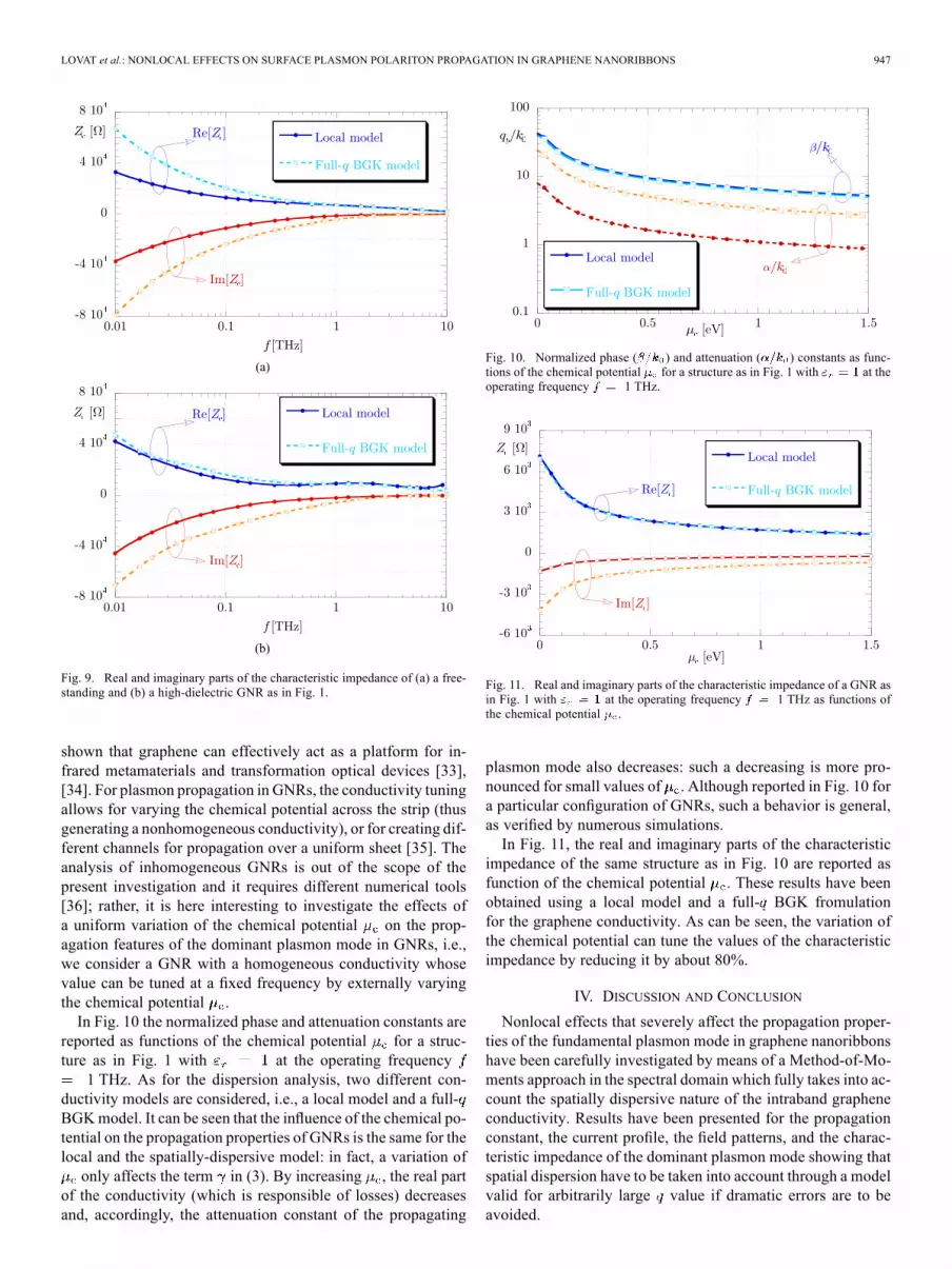
shown that graphene can effectively act as a platform for in-frared metamaterials and transformation optical devices [33],[34]. For plasmon propagation in GNRs, the conductivity tuningallows for varying the chemical potential across the strip (thusgenerating a nonhomogeneous conductivity), or for creating dif-ferent channels for propagation over a uniform sheet [35]. Theanalysis of inhomogeneous GNRs is out of the scope of thepresent investigation and it requires different numerical tools[36]; rather, it is here interesting to investigate the effects ofa uniform variation of the chemical potential on the prop-agation features of the dominant plasmon mode in GNRs, i.e.,we consider a GNR with a homogeneous conductivity whosevalue can be tuned at a fixed frequency by externally varyingthe chemical potential .In Fig. 10 the normalized phase and attenuation constants are
reported as functions of the chemical potential for a struc-ture as in Fig. 1 with at the operating frequency
1 THz. As for the dispersion analysis, two different con-ductivity models are considered, i.e., a local model and a full-BGKmodel. It can be seen that the influence of the chemical po-tential on the propagation properties of GNRs is the same for thelocal and the spatially-dispersive model: in fact, a variation of
only affects the term in (3). By increasing , the real partof the conductivity (which is responsible of losses) decreasesand, accordingly, the attenuation constant of the propagating
Fig. 10. Normalized phase ( ) and attenuation ( ) constants as func-tions of the chemical potential for a structure as in Fig. 1 with at theoperating frequency 1 THz.
Fig. 11. Real and imaginary parts of the characteristic impedance of a GNR asin Fig. 1 with at the operating frequency 1 THz as functions ofthe chemical potential .
plasmon mode also decreases: such a decreasing is more pro-nounced for small values of . Although reported in Fig. 10 fora particular configuration of GNRs, such a behavior is general,as verified by numerous simulations.In Fig. 11, the real and imaginary parts of the characteristic
impedance of the same structure as in Fig. 10 are reported asfunction of the chemical potential . These results have beenobtained using a local model and a full- BGK fromulationfor the graphene conductivity. As can be seen, the variation ofthe chemical potential can tune the values of the characteristicimpedance by reducing it by about 80%.
IV. DISCUSSION AND CONCLUSIONNonlocal effects that severely affect the propagation proper-
ties of the fundamental plasmon mode in graphene nanoribbonshave been carefully investigated by means of a Method-of-Mo-ments approach in the spectral domain which fully takes into ac-count the spatially dispersive nature of the intraband grapheneconductivity. Results have been presented for the propagationconstant, the current profile, the field patterns, and the charac-teristic impedance of the dominant plasmon mode showing thatspatial dispersion have to be taken into account through a modelvalid for arbitrarily large value if dramatic errors are to beavoided.

948 IEEE TRANSACTIONS ON TERAHERTZ SCIENCE AND TECHNOLOGY, VOL. 5, NO. 6, NOVEMBER 2015
In particular, it has been shown that the strongest nonlocaleffects occur for GNRs with small widths and supported by adielectric with high permittivity: usually the nonlocality largelyattenuates the longitudinal propagation of the plasmon modeand makes it slower at low frequencies and faster at high fre-quencies. The transverse profile of the longitudinal componentof the current is strongly modified showing a maximum at thecenter of the ribbon, while the modal field is less tightly con-fined to the ribbon. The characteristic impedance is less affectedby spatial dispersion, at least for high frequencies, whereas inthe low frequency (microwave) regime can be largely increasedboth in its resistive and capacitive part. Bias voltages or chem-ical doping can be effectively used to tune the modal proper-ties of the propagating SPP and, in particular, the former canbe used to locally modify the transverse conductivity profile tocreate a tunable inhomogeneous conductivity (this is left for fu-ture works).As concerns the effects that nonlocality may have on
graphene-based devices, the large variety of structures pro-posed in recent years, e.g., phase-shifters, filters, absorbers,prevents one from drawing sharp conclusions. However, inthe light of the results obtained in the present investigation,our feeling is that nonlocality does not necessarily spoil theexpected performance of GNR-based components, but, rather,it is a key parameter that must be taken into account in properdevice modeling and design.
APPENDIX
For completeness, we report in this Appendix the expres-sions of the dyadic elements for different graphene conductivitymodels derived in [9]. In particular, we show in a low- RTAmodel
(18)
whereas in a low- BGK model we have
(19)
In an RTA model, the dyadic conductivity elements whoseexpressions are instead valid for arbitrary values of are
(20)
where
(21)
with , , and
(22)
In a BGK full- model, we have
(23)
where
(24)
and with
(25)
Simpler expressions can be obtained in a polar coordinatesystem through the conventional longitudinal and transverse
representation [37]. In particular, in a low- approximation
(26)
(27)
while
(28)
and
(29)
whereas the relevant full- expressions are
(30)
(31)
with
(32)
LOVAT et al.: NONLOCAL EFFECTS ON SURFACE PLASMON POLARITON PROPAGATION IN GRAPHENE NANORIBBONS 949
for the BGK model and
(33)
(34)
for the RTA model. It should be noted that both and al-ways depend only on . This indicates that, in the absence ofmagnetic bias, graphene is modeled as an isotropic medium, thedyadic nature of its conductivity being uniquely due to the oc-currence of spatial dispersion.
REFERENCES
[1] C. Xu, H. Li, and K. Banerjee, “Modeling, analysis, and design ofgraphene nano-ribbon interconnects,” IEEE Trans. Electron Devices,vol. 56, no. 8, pp. 1567–1578, Aug. 2009.
[2] Y.-M. Lin, A. Valdes-Garcia, S.-J. Han, D. B. Farmer, I. Meric, Y. Sun,Y. Wu, C. Dimitrakopoulos, A. Grill, P. Avouris, and K. A. Jenkins,“Wafer-scale graphene integrated circuits,” Science, vol. 332, no. 10,pp. 1294–1297, Mar. 2011.
[3] J.-P. Cui,W.-S. Zhao,W.-Y. Yin, and J. Hu, “Signal transmission anal-ysis of multilayer graphene nano-ribbon (MLGNR) interconnects,”IEEE Trans. Electromagn. Compat., vol. 54, no. 1, pp. 126–132, Feb.2012.
[4] A. Y. Nikitin, F. Guinea, F. J. García-Vidal, and L. Martín-Moreno,“Edge and waveguide TERAHERTZ surface plasmon modes ingraphene microribbons,” Phys. Rev. B, vol. 84, Oct. 2011, Art. ID161407.
[5] J. Christensen, A. Manjavacas, S. Thongrattanasiri, F. H. L. Koppens,and F. J. García de Abajo, “Graphene plasmon waveguiding and hy-bridization in individual and paired nanoribbons,” ACS Nano, vol. 6,no. 1, pp. 431–440, 2012.
[6] F. H. L. Koppens, D. E. Chang, and F. J. Garcia de Abajo, “Grapheneplasmonics: A platform for strong light-matter interactions,” NanoLett., vol. 11, no. 8, pp. 3370–3377, 2011.
[7] M. Jablan, M. Soljacic, and H. Buljan, “Plasmons in graphene: Fun-damental properties and potential applications,” Proc. IEEE, vol. 101,no. 7, pp. 1689–1704, Sep. 2013.
[8] G. W. Hanson, “Dyadic Green's functions for an anisotropic non-localmodel of biased graphene,” IEEE Trans. Antennas Propag., vol. 56,no. 3, pp. 747–757, Mar. 2008.
[9] G. Lovat, G. W. Hanson, R. Araneo, and P. Burghignoli, “Semiclas-sical spatially dispersive intraband conductivity tensor and quantumcapacitance of graphene,” Phys. Rev. B, vol. 87, no. 11, Mar. 2013,Art. ID 115429.
[10] G. Lovat, P. Burghignoli, and R. Araneo, “Low-frequency dominant-mode propagation in spatially-dispersive graphene nano-waveguides,”IEEE Trans. Electromagn. Compat., vol. 55, no. 1, pp. 101–109, Feb.2013.
[11] J. Gomez-Diaz, J. Mosig, and J. Perruisseau-Carrier, “Effect of spatialdispersion on surface waves propagating along graphene sheets,” IEEETrans. Antennas Propag., vol. 61, no. 7, pp. 3589–3596, Jul. 2013.
[12] D. Correas-Serrano, J. Gomez-Diaz, J. Perruisseau-Carrier, and A. Al-varez-Melcon, “Spatially dispersive graphene single and parallel platewaveguides: Analysis and circuit model,” IEEE Trans. Microw. TheoryTechn., vol. 61, no. 12, pp. 4333–4344, Dec. 2013.
[13] D. Correas-Serrano, J. Gomez-Diaz, and A. Alvarez-Melcon, “On theinfluence of spatial dispersion on the performance of graphene-basedplasmonic devices,” IEEE Antennas Wireless Propag. Lett., vol. 13, pp.345–348, 2014.
[14] X. Zhu, W. Yan, N. A. Mortensen, and S. Xiao, “Bends and splittersin graphene nanoribbon waveguides,” Opt. Exp,, vol. 21, no. 3, pp.3486–3491, Feb. 2013.
[15] W. Wang and J. M. Kinaret, “Plasmons in graphene nanoribbons: In-terband transitions and nonlocal effects,” Phys. Rev. B, vol. 87, May2013, Art. ID 195424.
[16] J. Chen et al., “Optical nano-imaging of gate tunable graphene plas-mons,” Nature, vol. 487, no. 7405, pp. 77–81, 2012.
[17] Z. Fei et al., “Gate-tuning of graphene plasmons revealed by infrarednano-imaging,” Nature, vol. 487, no. 7405, pp. 82–85, 2012.
[18] W. Gao, J. Shu, C. Qiu, and Q. Xu, “Excitation of plasmonic waves ingraphene by guided-mode resonances,” ACS Nano, vol. 6, no. 9, pp.7806–7813, 2012.
[19] W. Gao, G. Shi, Z. Jin, J. Shu, Q. Zhang, R. Vajtai, P. M. Ajayan, J.Kono, and Q. Xu, “Excitation and active control of propagating surfaceplasmon polaritons in graphene,” Nano Lett., vol. 13, pp. 3698–3702,2013.
[20] Y. Bludov, A. Ferreira, N.M. R. Peres, andM. I. Vasilevskiy, “A primeron surface plasmon-polaritons in graphene,” Int. J. Mod. Phys. B, vol.27, no. 10, 2013, Art. ID 1341001.
[21] W. Liu, J. Wei, X. Sun, and H. Yu, “A study on graphene—metal con-tact,” Crystals, vol. 3, no. 1, pp. 257–274, 2013.
[22] L. A. Falkovsky, “Optical properties of graphene and IV – VI semicon-ductors,” Physics-Uspekhi, vol. 51, no. 9, p. 887, 2008.
[23] M. Havrilla and D. Nyquist, “Full-wave analysis of an imperfectly-conducting stripline,” J. Electromagn. Waves Applicat., vol. 16, no. 6,pp. 739–755, 2002.
[24] T. Ooura and M. Mori, “A robust double exponential formula forFourier-type integrals,” J. Comput. Appl. Math., vol. 112, pp. 229–241,1999.
[25] C. Gillan, A. Schuchinsky, and L. Spence, “Computing zeros ofanalytic functions in the complex plane without using derivatives,”Comput. Phys. Commun., vol. 175, no. 4, pp. 304–313, Aug. 2006.
[26] R. Rodríguez-Berral, F.Mesa, and F.Medina, “Systematic and efficientroot finder for computing the modal spectrum of planar layered waveg-uides,” Int. J. RF Microw. Comput. Eng., vol. 14, no. 1, pp. 73–83, Jan.2004.
[27] K. A. Michalski and J. R. Mosig, “Multilayered media Green'sfunctions in integral equation formulations,” IEEE Trans. AntennasPropag., vol. 45, no. 3, pp. 508–519, Mar. 1997.
[28] J. Brews, “Characteristic impedance of microstrip lines,” IEEE Trans.Microw. Theory Techn., vol. MTT-35, no. 1, pp. 30–34, Jan. 1987.
[29] F. J. García de Abajo, “Nonlocal effects in the plasmons of stronglyinteracting nanoparticles, dimers, and waveguides,” J. Phys. ChemistryC, vol. 112, no. 46, pp. 17983–17987, 2008.
[30] A. Fallahi and J. Perruisseau-Carrier, “Design of tunable biperiodicgraphene metasurfaces,” Phys. Rev. B, vol. 86, Nov. 2012, Art. ID195408.
[31] M. Esquius-Morote, J. Gomez-Diaz, and J. Perruisseau-Carrier, “Sinu-soidally modulated graphene leaky-wave antenna for electronic beam-scanning at THz,” IEEE Trans. THz Sci. Technol., vol. 4, no. 1, pp.116–122, Jan. 2014.
[32] P.-Y. Chen and A. Alù, “Atomically thin surface cloak using graphenemonolayers,” ACS Nano, vol. 5, no. 7, pp. 5855–5863, 2011.
[33] A. Vakil and N. Engheta, “Transformation optics using graphene,” Sci-ence, vol. 332, no. 6035, pp. 1291–1294, 2011.
[34] S.Maci, G.Minatti,M. Casaletti, andM.Bosiljevac, “Metasurfing: Ad-dressing waves on impenetrable metasurfaces,” IEEE Antennas Wire-less Propag. Lett., vol. 10, pp. 1499–1502, 2011.
[35] E. Forati and G. W. Hanson, “Soft-boundary graphene nanoribbonformed by a graphene sheet above a perturbed ground plane: Conduc-tivity profile and SPP modal current distribution,” J. Opt., vol. 16, no.8, p. 089501, 2014.
[36] P. Burghignoli, R. Araneo, G. Lovat, and G. Hanson, “Space-domainmethod of moments for graphene nanoribbons,” inProc. 8th Eur. Conf.Antennas and Propagat., Apr. 2014, pp. 666–669.
[37] M. Dressel and G. Grüner, Electrodynamics of Solids. Cambridge,U.K.: Cambridge Univ., 2002.
Giampiero Lovat (S'02–M'06) received the Ph.D.degree in applied electromagnetics from the Univer-sity of Rome “Sapienza”, Rome, Italy, in 2005.He is currently an Assistant Professor with the
Astronautical, Electrical, and Energetic EngineeringDepartment, University of Rome “Sapienza,” Rome,Italy. He is a coauthor of “Fast Breaking Papers,October 2007” in EE and CS, about metamaterials.He coauthored the book Electromagnetic Shielding(IEEE–Wiley, 2008). His present research interestsinclude leaky waves, periodic structures, electro-
magnetic shielding, and nanoelectromagnetics.Dr. Lovat was the recipient of the Young Scientist Award from the 2005 URSI
General Assembly, New Delhi, India, and in 2011, he was the recipient of theBest Paper Symposium Award at the 2011 IEEE EMC-S International Sympo-sium on Electromagnetic Compatibility.

950 IEEE TRANSACTIONS ON TERAHERTZ SCIENCE AND TECHNOLOGY, VOL. 5, NO. 6, NOVEMBER 2015
Rodolfo Araneo (M'03–SM'10) received the Ph.D.degree in electrical engineering from the Universityof Rome “Sapienza”, Rome, in 2002.He was a Visiting Student with the National
Institute of Standards and Technology (NIST)Boulder, CO, USA, where he worked on TEM cellsand shielding, and a Visiting Researcher of theDepartment of Electrical and Computer Engineeringof University of Missouri-Rolla (UMR) where heworked on printed circuit boards and finite-differ-ence time-domain techniques. His research activity
is mainly in the field of electromagnetic compatibility (EMC) and includesnumerical and analytical techniques for modelling high-speed printed circuitboards, shielding, and transmission line analysis.Dr. Araneo received the Past President's Memorial Award in 1999 from
the IEEE Electromagnetic Compatibility Society. He is the present generalchair of the IEEE International Conference on Environment and ElectricalEngineering.
Paolo Burghignoli (S'97–M'01–SM'08) was born inRome, Italy, on February 18, 1973. He received theLaurea degree (cum laude) in electronic engineeringand Ph.D. degree in applied electromagnetics fromthe University of Rome “Sapienza”, Rome, Italy, in1997 and 2001, respectively.In 1997, he joined the Electronic Engineering De-
partment, now the Department of Information Engi-neering, Electronics and Telecommunications, Uni-versity of Rome “La Sapienza”, Rome, Italy, where,since November 2010, he has been an Assistant Pro-
fessor. From January 2004 to July 2004, he was a Visiting Research AssistantProfessor with the University of Houston, Houston, TX, USA. His scientificinterests include analysis and design of planar antennas and arrays, leakagephenomena in uniform and periodic structures, numerical methods for integralequations and periodic structures, propagation and radiation in metamaterials,
ground-penetrating radars, scattering frommoving objects, and electromagneticshielding.Dr. Burghignoli was the recipient of the “Giorgio Barzilai” Laurea Prize
(1996–1997) presented by the former IEEE Central & South Italy Section, a2003 IEEE Microwave Theory and Techniques Society (MTT-S) Graduate Fel-lowship, and a 2005 Raj Mittra Travel Grant for Junior Researchers presentedat the IEEE Antennas and Propagation Society Symposium on Antennas andPropagation, Washington, DC, USA. He is a coauthor of the “Fast BreakingPapers, October 2007” in EE and CS, about metamaterials (paper that had thehighest percentage increase in citations in Essential Science Indicators, ESI).
George W. Hanson (S'85–M'91–SM'98–F'09) wasborn in Glen Ridge, NJ, USA, in 1963. He receivedthe B.S.E.E. degree from Lehigh University, Beth-lehem, PA, USA, in 1986, the M.S.E.E. degree fromSouthern Methodist University, Dallas, TX, USA, in1988, and the Ph.D. degree fromMichigan State Uni-versity, East Lansing, MI, USA, in 1991.From 1986 to 1988, he was a Development Engi-
neer with General Dynamics, Fort Worth, TX, USA,where he worked on radar simulators. From 1988 to1991, he was a Research and Teaching Assistant with
the Department of Electrical Engineering, Michigan State University. He is cur-rently a Professor of electrical engineering and computer science with the Uni-versity of Wisconsin-Milwaukee, Milwaukee, WI, USA. He is coauthor of thebook Operator Theory for Electromagnetics: An Introduction (Springer, 2002)and author of Fundamentals of Nanoelectronics (Prentice-Hall, 2007). His re-search interests include nanoelectromagnetics, quantum optics, mathematicalmethods in electromagnetics, and electromagnetic wave phenomena in layeredmedia.Dr. Hanson is a member of URSI Commission B, Sigma Xi, and Eta Kappa
Nu, and was an associate editor for the IEEE TRANSACTIONS ON ANTENNASAND PROPAGATION from 2002 to 2007. In 2006, he was the recipient of theS.A. Schelkunoff Best Paper Award from the IEEE Antennas and PropagationSociety.


