Embed Size (px)
Citation preview

ESCUELA TÉCNICA SUPERIOR DE INGENIERÍA
[RETROFIT DE UN SISTEMA FOTOVOLTAICO
DE SEGUIMIENTO SOLAR]
2014
Proyecto Final de Carrera
Ingeniero en Automática y Electrónica
Industrial
Autor: Diego Aragón Rodríguez
Tutor: Luis Fernando Castaño Castaño

0 Proyecto Final de Carrera
RETROFIT DE UN SISTEMA FOTOVOLTAICO DE SEGUIMIENTO SOLAR
Índice

Proyecto Final de Carrera
RETROFIT DE UN SISTEMA FOTOVOLTAICO DE SEGUIMIENTO SOLAR
1
Resumen del proyecto. ............................................................................................. 3
Objetivo del proyecto. .............................................................................................. 5
1. Estudio previo ................................................................................................... 8
1.1. Estado del arte de seguidores solares de dos grados de libertad. .................. 8
1.1.1. Introducción. ......................................................................................................... 8
1.1.2. Energía solar fotovoltaica. ..................................................................................... 9
1.1.3. Tipos de instalaciones comerciales. .................................................................... 16
1.1.4. Métodos de seguimientos. .................................................................................. 20
1.2. Estudio de los dispositivos de seguimiento existente en el departamento. 21
1.2.1. “Simulador de sistema de control para seguimiento solar de dos ejes” ............ 21
1.2.2. “Sistema de control de precisión para seguimiento solar en dos ejes” .............. 21
2. Fase de actuación sobre la estructura mecánica ............................................... 23
3. Fase de actuación sobre los paneles solares e inversor ..................................... 31
4. Fase de actuación sobre la unidad de control ................................................... 38
4.1. PLC OMRON ..................................................................................................... 52
4.1.1. PLC CJ1M ............................................................................................................. 53
4.1.2. Instalación CX-Programmer V5.0. ....................................................................... 61
4.1.3. Cables para conexión .......................................................................................... 61
4.1.4. Crear nuevo proyecto con CX-Programmer. ....................................................... 63
4.1.5. Definiendo Tabla de E/S. ..................................................................................... 66
4.1.6. Definiendo el bastidor principal. ......................................................................... 66
4.1.7. Compilando y conectando. .................................................................................. 67
4.1.8. Transfiriendo información desde el PC al PLC. .................................................... 67
4.1.9. Monitorizando y modos de funcionamiento....................................................... 69
4.1.10. Conexión Ethernet. .............................................................................................. 70
4.1.11. IP del PC. .............................................................................................................. 70
4.1.12. Enviar y recibir datos a través del puerto RS-232C. ............................................ 71
4.1.13. Hyperterminal. .................................................................................................... 72
4.1.14. @TXD & @RXD. ................................................................................................... 72
4.1.15. LabView. .............................................................................................................. 75
4.2. PLC SCHNEIDER ELECTRIC M238 ..................................................................... 87
5. Fase de actuación sobre elementos auxiliares .................................................. 91
5.1. Sensor solar ISS-AX (Analógico) ...................................................................... 93

2 Proyecto Final de Carrera
RETROFIT DE UN SISTEMA FOTOVOLTAICO DE SEGUIMIENTO SOLAR
5.2. Sensor solar ISS-DX (Digital) ........................................................................... 95
5.3. Sensor solar ISS-CYPA (Cilindro Parabólico) ................................................... 97
5.4. Sensor solar NANO-ISS60 (NANO) .................................................................. 98
6. Conclusiones ................................................................................................. 102
7. Bibliografía y Programas utilizados ................................................................ 103
8. Anexos .......................................................................................................... 104
Proyecto Final de Carrera
RETROFIT DE UN SISTEMA FOTOVOLTAICO DE SEGUIMIENTO SOLAR
3
Resumen del proyecto.
Este proyecto se plantea con el objetivo de hacer un estudio detallado de una instalación de seguidor solar existente con el fin de actualizarla.
La instalación inicialmente fue diseñada como planta experimental donde se
han llevado a cabo ensayos de controladores y ha estado operativa durante un tiempo.
Sin embargo, los últimos intentos de puesta en funcionamiento han dado resultados
negativos. Descartados fallos menores como fallos en los conectores, fusibles y fuentes
de alimentación, etc., se constata la necesidad de hacer un análisis más detallado de
todos los equipos implicados y se decide hacer un retrofit de la instalación completa,
tanto de la parte mecánica como de la parte de control.
Teniendo en cuenta que las averías podrían provenir tanto de los equipos
eléctricos y electrónicos como en los equipos mecánicos, se ha procedido a analizar el
estado de cada uno de éstos de forma separada y en el caso de detectar fallo, estudiar
la posibilidad de reparación o proponer equipos nuevos que los sustituyan.
El proyecto se ha estructurado de la siguiente forma:
1- Se ha realizado una presentación inicial del estado del arte de este tipo de
instalaciones, para que en caso de hacer alguna propuesta de modificación de
alguna parte se dispusiera de una información actualizada.
2- Se ha estudiado la documentación disponible, principalmente los trabajos
publicados sobre la instalación, concretamente proyectos fin de carrera y
manuales.
3- Se hizo una búsqueda adicional de información a través de otros medios,
(internet, empresas suministradoras, etc.). Clasificándola y presentándola de
forma fácilmente accesible como anexos del proyecto.
4- Se evaluó la parte mecánica del seguidor. Se constató que no funcionaba en
elevación. Después de desmontar y engrasar se comprobó su buen
funcionamiento, por lo que se propuso conservar este elemento.
5- Se evaluó la parte eléctrica (paneles e inversor) comprobando su buen
funcionamiento por lo que se propuso mantener estos elementos.
6- Se evaluó el bloque controlador, constatando que la parte de potencia
(amplificadores de motores) puede seguir usándose, sin embargo la electrónica
asociada a los accionadores presentan deficiencias importantes. Se concluye
sustituir esta electrónica específica por una de propósito general basada en
PLC.
7- Se probó experimentalmente la viabilidad de uso de un PLC sin tarjetas de
contaje rápido. Se presentaron las limitaciones de esta opción. Se propuso la

4 Proyecto Final de Carrera
RETROFIT DE UN SISTEMA FOTOVOLTAICO DE SEGUIMIENTO SOLAR
compra de un autómata nuevo con entradas rápidas adaptadas a la lectura de
encoder.
8- Se evaluó los sensores auxiliares de irradiancia, comprobando que están
operativos, por lo que también se propuso utilizar este dispositivo.
9- Se propusieron completar la información sensorial con nuevos sensores de
orientación que enriquezcan la planta de investigación.
10- También se propusieron reemplazar los módulos fotovoltaicos existentes por
módulos de alta concentración CPV dotando a nuestro sistema de mayor
captación solar. Se propuso incluir un anemómetro en nuestro sistema para
evitar posibles roturas causadas por la fuerza del viento.
11- Se generó nueva documentación que carecía la instalación actual (cableado y
esquemas eléctricos) así como se saneó cableado existente.
12- Se comprobó la correcta comunicación entre PLC y PC vía serie.

Proyecto Final de Carrera
RETROFIT DE UN SISTEMA FOTOVOLTAICO DE SEGUIMIENTO SOLAR
5
Objetivo del proyecto.
El título del proyecto “RETROFIT DE UN SISTEMA FOTOVOLTAICO DE
SEGUIMIENTO SOLAR” describe de forma muy general el contenido del mismo, por lo
que conviene especificar y concretar más los objetivos marcados.
En primer lugar este tipo de proyecto se encuadra dentro de los denominados
“retrofit”, que podría definirse da la siguiente manera, Retrofit: es una técnica de
renovación de instalaciones, equipos, maquinaria basada en la actualización de
componentes o accesorios más modernos o eficaces que los disponibles, o donde estos
no existían. Se utiliza especialmente en algunos sectores industriales donde la
renovación completa de máquinas, sistemas y equipos tiene costes muy elevados. Se
reemplazan equipos ya obsoletos y se conserva la parte mecánica en buen estado como
es la estructura propia.
En el caso del presente proyecto se parte de una instalación fotovoltaica
formada por un seguidor solar que dispone de una serie de equipos auxiliares de
control y supervisión. Esta instalación en su día fue diseñada como planta
experimental donde poder llevar a cabo ensayos de controladores. Inicialmente se
disponía de un ordenador desde donde se podía supervisar la instalación mediante la
conexión con Labview a través de un puerto serie.
La instalación sirvió en su momento como plataforma en proyectos de
investigación y la realización de proyectos fin de carrera. Pero con el paso del tiempo y
tras un periodo de inactividad, se constató que presentaba fallos de funcionamiento al
tratar de ponerla de nuevo operativa. Por otra parte, la falta de documentación de
algunos de sus equipos o componentes hacía muy costosos los intentos de puesta en
marcha.
En este punto se decide proponer este proyecto, que consiste en hacer primero
un estudio detallado de la planta existente, evaluando los equipos y el software. En
base a la información recabada se propone las modificaciones necesarias a realizar
para que la planta vuelva a estar operativa, proponiendo mejoras tecnológicas que
renueven la instalación.
Para todo ello se intentará aprovechar al máximo todos los componentes de
que se dispone y se decidirá en el momento que se determine en la compra de nuevos
componentes necesarios para tal finalidad o por el contrario el arreglo de lo que se
necesite.
Otro de los objetivos principales del proyecto es dejar bien argumentado y
documentado todo lo observado así como todos los cambios aplicados para que
cualquiera que quiera retomarlo, con tan sólo una lectura de este documento, pueda

6 Proyecto Final de Carrera
RETROFIT DE UN SISTEMA FOTOVOLTAICO DE SEGUIMIENTO SOLAR
conocer en qué estado se encuentra todas sus partes y como proceder para poder
emprender su nueva aplicación. También podrá disponer a modo de consulta los
anexos de este proyecto donde podrá encontrar datasheets que facilitarán en su
mayor medida la consulta deseada.

Proyecto Final de Carrera
RETROFIT DE UN SISTEMA FOTOVOLTAICO DE SEGUIMIENTO SOLAR
7
Para llevar una coherencia con el proceso seguido primero se ha realizado un
estudio previo, encontrando dos partes bien diferenciadas dentro de este estudio, una
primera parte denominada estado del arte donde se ha realizado una presentación de
instalaciones similares a la nuestra para poder tener información actualizada en el caso
de realizar alguna propuesta, y una segunda parte donde se ha estudiado la
documentación de la que se dispone de nuestra instalación en cuestión.
Se ha continuado con diferentes fases de actuaciones, en concreto de cuatro,
donde se detallan las diferentes intervenciones en las distintas partes de nuestro
seguidor donde se observará el estado de cada parte, y si se procede a reutilizarla o se
descarta así como posibles sustituciones por otros equipos.
- Fase de actuación sobre la estructura mecánica: se describe las distintas partes
de la que consta la estructura mecánica, así como las diferentes pruebas
realizadas para determinar el estado de todas las partes que la componen y
poder concluir si se siguen utilizando.
- Fase de actuación sobre los paneles solares e inversor: en esta fase al igual que
la anterior se hace una presentación de los equipos, en este caso del panel
solar utilizado así como del inversor de cc/ca evaluando cada uno de ellos. En
esta fase se propone la sustitución de los actuales paneles por otros de
concentración solar. Y al igual que en la anterior fase se concluye la posible
reutilización de los mismos.
- Fase de actuación sobre la unidad de control: esta fase constituye el corazón de
nuestra instalación, la que controlará la forma y modo de movimiento de todas
las demás partes. Se detalla y evalúa las distintas partes que la conforman y se
toma la decisión de reemplazar o no el actual sistema de control.
- Fase de actuación sobre elementos auxiliares: en esta última fase se describe y
se evalúa el sensor de irradiancia del que dispone nuestra instalación sus
características así como su propuesta de sustitución por unos sensores solares
más actuales. También se propone la utilización de un anemómetro. Se
concluye con la posibilidad o no de la utilización del sensor de irradiancia.
Una vez que se termina las distintas fases se concluye con una estructura de los
elementos que se utilizan finalmente y los que se descartan así como las propuestas de
sustitución a modo de resumen. Más adelante se dispone de la bibliografía utilizada así
como los softwares con sus versiones utilizadas. Y para terminar se puede observar un
anexo donde se encontrará información más detallada de cada uno de los elementos
utilizados.

8 Proyecto Final de Carrera
RETROFIT DE UN SISTEMA FOTOVOLTAICO DE SEGUIMIENTO SOLAR
1. Estudio previo
En este estudio previo se va a realizar una presentación del estado del arte de
este tipo de instalaciones para que en caso de hacer alguna propuesta de modificación
de alguna parte se dispusiera de una información actualizada. A continuación del
estudio previo se dispondrá un estudio de la documentación de la que se dispone de
nuestra instalación en cuestión.
1.1. Estado del arte de seguidores solares de dos grados de libertad.
Se describirá las distintas maneras o formas que actualmente se puede
encontrar un sistema fotovoltaico de seguimiento solar ya sea fijo, de 1 ó 2 grados de
libertad.
1.1.1. Introducción.
El modelo actual de desarrollo se ha basado históricamente en el uso y
explotación de los recursos energéticos de origen fósil. Estos combustibles han
suministrado las fuentes energéticas del desarrollo económico del planeta, de manera
intensiva desde el nacimiento de la Revolución Industrial hasta nuestros días.
Este acelerado desarrollo, sin embargo, también ha generado voces de alerta
sobre impactos ambientales que genera la explotación de los recursos que, por su
lenta velocidad de regeneración respecto de su explotación, son clasificados como no
renovables. Los impactos ambientales que estos combustibles generan (cambio
climático, lluvia ácida, capa de ozono), ha obligado a la comunidad internacional a
buscar un nuevo modelo de desarrollo (Desarrollo Sostenible), sin comprometer las
necesidades de las futuras generaciones.
A lo anterior se suma la creciente incertidumbre respecto del suministro de
combustibles fósiles, por el constante clima de tensión en los países productores de
petróleo, y a nivel local, la necesidad de una diversificación de la matriz energética en
la región y en el país, que permita sobrellevar de mejor manera los problemas
coyunturales.
En este ámbito, los países desarrollados, en especial, la Unión Europea han sido
los pioneros en la búsqueda de nuevas alternativas de suministro energético.
Proyecto Final de Carrera
RETROFIT DE UN SISTEMA FOTOVOLTAICO DE SEGUIMIENTO SOLAR
9
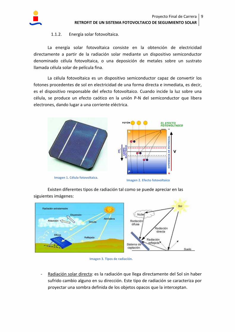
1.1.2. Energía solar fotovoltaica.
La energía solar fotovoltaica consiste en la obtención de electricidad
directamente a partir de la radiación solar mediante un dispositivo semiconductor
denominado célula fotovoltaica, o una deposición de metales sobre un sustrato
llamada célula solar de película fina.
La célula fotovoltaica es un dispositivo semiconductor capaz de convertir los
fotones procedentes de sol en electricidad de una forma directa e inmediata, es decir,
es el dispositivo responsable del efecto fotovoltaico. Cuando incide la luz sobre una
célula, se produce un efecto caótico en la unión P-N del semiconductor que libera
electrones, dando lugar a una corriente eléctrica.
Existen diferentes tipos de radiación tal como se puede apreciar en las
siguientes imágenes:
Imagen 3. Tipos de radiación.
- Radiación solar directa: es la radiación que llega directamente del Sol sin haber
sufrido cambio alguno en su dirección. Este tipo de radiación se caracteriza por
proyectar una sombra definida de los objetos opacos que la interceptan.
Imagen 1. Célula fotovoltaica. Imagen 2. Efecto fotovoltaico

10 Proyecto Final de Carrera
RETROFIT DE UN SISTEMA FOTOVOLTAICO DE SEGUIMIENTO SOLAR
- Radiación solar difusa: una parte de la radiación que atraviesa la atmósfera es
reflejada por las nubes o absorbida por éstas. Esta radiación, llamada difusa, va
en todas direcciones, efecto producido por las reflexiones y absorciones, no
sólo de las nubes sino de las partículas de polvo atmosférico, montaña, árboles,
edificios, el propio suelo, etc. Este tipo de radiación se caracteriza por no
producir sombra alguna respecto a los objetos opacos interpuestos. Las
superficies horizontales son las que más radiación difusa reciben, ya que ven
toda la bóveda celeste, mientras que las verticales reciben menos porque sólo
ven la mitad.
- Radiación solar reflejada: Este tipo de radiación solar es la que refleja la
superficie terrestre. La cantidad de radiación depende del coeficiente de
reflexión de la superficie, también llamado albedo. Las superficies horizontales
no reciben ninguna radiación reflejada, porque no ven ninguna superficie
terrestre y las superficies verticales son las que más radiación reflejada reciben.
- Radiación solar global: La radiación solar global es la radiación total. Esta
constituye la suma de las tres radiaciones anteriormente nombradas.
En un día despejado, la radiación directa es preponderante sobre la radiación
difusa. Por el contrario, en un día nublado no hay radiación directa y la
totalidad de la radiación que incide es difusa.
En la fig. 4 se observa la relación de la radiación solar a nivel de superficie
terrestre.
Imagen 4. Radiación solar que llega a la superficie terrestre.

Proyecto Final de Carrera
RETROFIT DE UN SISTEMA FOTOVOLTAICO DE SEGUIMIENTO SOLAR
11
Este tipo de energía se usa para alimentar innumerables aparatos autónomos.
Debido a la creciente demanda de energías renovables, la fabricación de células
solares e instalaciones fotovoltaicas ha avanzado considerablemente en los últimos
años. A continuación, en la fig. 5, se puede observar la radiación solar que llega a
Europa:
Los rendimientos típicos de una célula fotovoltaica de silicio policristalino oscilan
entre el 14%-20%. Para células de silicio monocristalino, los valores oscilan entre el
15%-21%. En la siguiente imagen se puede apreciar los dos tipos mencionados:
Los paneles solares fotovoltaicos no producen calor que se pueda reaprovechar.
Para incentivar el desarrollo de la tecnología con miras a alcanzar la paridad de red –
igualar el precio de obtención de la energía al de otras fuentes más económicas en la
Imagen 5. Radiación solar que llega a Europa.
Imagen 6. Monocristalino Vs Policristalino

12 Proyecto Final de Carrera
RETROFIT DE UN SISTEMA FOTOVOLTAICO DE SEGUIMIENTO SOLAR
actualidad-, existen primas a la producción, que garantizan un precio fijo de compra
por parte de la red eléctrica, es el caso de Alemania, Italia o España. Según un estudio
publicado en 2007 por el World Energy Council, para el año 2100 el 70% de la energía
consumida será de origen solar según informes de Greenpeace, la fotovoltaica podrá
suministrar electricidad a dos tercios de la población mundial en 2030. España es uno
de los países con unas condiciones excepcionales como se puede observar en la fig. 7,
en lo que a condiciones de radiación solar se refiere:
Se puede distinguir los siguientes tipos de instalaciones fotovoltaicas:
- Instalación solar fotovoltaica fija:
Se denomina de esta forma a las plantas fotovoltaicas cuyos paneles
permanecen en la misma posición a lo largo del tiempo, como se puede
apreciar en la fig. 8.
Imagen 7. Radiación solar que llega a España
Imagen 8. Instalación solar fotovoltaica fija.

Proyecto Final de Carrera
RETROFIT DE UN SISTEMA FOTOVOLTAICO DE SEGUIMIENTO SOLAR
13
- Instalación solar fotovoltaica 1 eje.
Se utiliza el concepto de seguidor solar: máquina con una parte fija y otra móvil
que dispone una superficie de captación solar lo más perpendicular al sol
posible a lo largo del día y dentro de sus rangos de movimiento.
Se denomina seguidor a un eje a seguidores que sólo gozan de un grado de
libertad en su movimiento. En la fig. 9 se observa lo comentado.
Imagen 9. Instalación solar fotovoltaica 1 eje.
Este tipo de sistemas es el más usado, debido a que la máxima variación entre
sol y panel ocurre en azimut, la variación en elevación se desprecia por considerarse de
poca repercusión en términos de energía y porque se encarecen los costos de
desarrollo. Sin embargo, la elevación se realiza de forma manual cada 6 meses, para
temporada invernal y estival, o bien se puede fijar en la mitad, para ambas estaciones.
- Instalación solar fotovoltaica 2 ejes.
Se trata de seguidores con dos grados de libertad, capaces de hacer un
seguimiento solar más preciso.
Imagen 10. Instalación solar fotovoltaica 2 ejes.

14 Proyecto Final de Carrera
RETROFIT DE UN SISTEMA FOTOVOLTAICO DE SEGUIMIENTO SOLAR
Este tipo de sistemas es un poco menos común aunque cada vez se pueden
encontrar más, estos siguen el sol tanto en dirección como en elevación, lo que implica
tener dos actuadores, para variar la inclinación del panel en forma horizontal y vertical.
En la fig. 10 se puede observar este tipo de instalación, en concreto la que nos atañe
para este proyecto.
Al orientar los paneles fotovoltaicos de forma perpendicular al sol se
incrementa la energía recibida. En la siguiente imagen se muestra una gráfica
comparativa entre los tres tipos de instalaciones tratados, observando la productividad
de cada uno de ellos:
Comparación entre seguidores de un eje y seguidores de dos ejes:
Ventajas Inconvenientes
Un Eje -Menor coste -Seguimiento solar impreciso -Simplicidad -Menor energía captada -Posibilidad de adaptación a cubiertas
Dos ejes -Seguimiento solar más preciso -Mayor coste -Incrementos de la producción en torno al 35% con
respecto a una planta fija
-Generalmente dificultan el robo de paneles FV
Anteriormente se ha comentado orientaciones en elevación y en azimut, a
continuación se muestra una imagen donde se puede observar ambas posiciones:
Imagen 11. Comparativa tipos de instalación

Proyecto Final de Carrera
RETROFIT DE UN SISTEMA FOTOVOLTAICO DE SEGUIMIENTO SOLAR
15
Imagen 12. Elevación y Acimut
La variación de la elevación del sol se produce por la inclinación del eje de
rotación terrestre, de 23,5⁰ aproximadamente con respecto al plano de la órbita que
describe alrededor del sol y da origen a las estaciones del año, tal como se puede
apreciar en la fig. 13.
Imagen 13. Variación de la elevación del sol.

16 Proyecto Final de Carrera
RETROFIT DE UN SISTEMA FOTOVOLTAICO DE SEGUIMIENTO SOLAR
1.1.3. Tipos de instalaciones comerciales.
En este punto se recogen una serie de instalaciones comerciales basadas todas
ellas en sistemas de seguimientos en dos ejes y con diferentes métodos de control.
• SUNTRACK 5: Es un sistema basado en micro controlador, que ha sido diseñado
para seguimiento en dos eje con alta precisión. El módulo de control es
adaptable para sistemas hidráulicos y eléctricos. Este sistema trabaja
calculando la posición del sol (programación astronómica), tanto en Azimut
como en Elevación, con una precisión de 0.01⁰.
Dimensiones: 105x103x30mm.
Alimentación: 24 V (± 20%),
10 A /+10%).
Entradas digitales: 4.
Salidas digitales: 4.
Entrada analógica: 1 (0 a 10 V).
Salidas analógicas: 2 (0 a 10 V).
Entradas encoders: 6 entradas digitales (24 V/30 mA). Precisión: > 0.015⁰
Ver fig. 14.
• SDK TRACKER-KIT: SDK ha adaptado el modelo de seguidor solar a dos ejes
TRACKER-KIT para ser utilizado como estructura de seguimiento para paneles
solares de concentración (CPV), con una precisión en el seguimiento de 0.1⁰, la
cual busca garantizar la captación solar óptima en la tecnología de
concentración.
Potencia del seguidor: 15 kW.
Movimiento en 2 ejes: 2 actuadores lineales y 1 motor reductor planetario (2
motores eléctricos).
Rotación en eje horizontal (Elevación): de 0⁰ a 70⁰.
Rotación en eje vertical (Azimut): de 0⁰ a 240⁰.
Altura (máxima): 4.50 m.
Ancho (máximo): 14.50 m.
Imagen 14. Suntrack 5.
Ver fig. 15.
Imagen 15. SDK Tracker-Kit.

Proyecto Final de Carrera
RETROFIT DE UN SISTEMA FOTOVOLTAICO DE SEGUIMIENTO SOLAR
17
• Mecasolar MS-2 Tracker 10: Es un equipo electromecánico que en su parte
superior lleva fijados los módulos fotovoltaicos y que consigue que la insolación
sobre los mismos sea máxima; toda esta estructura se mueve de Este a Oeste
sobre un eje que puede girar 240⁰ (seguimiento acimutal) y un segundo eje con
movimiento de inclinación desde los 60⁰ hasta la posición horizontal.
Ejes de seguimiento: 2 ejes: horizontal y vertical.
Potencia admitida en seguidor: hasta 12 kW.
Ángulo giro: Eje vertical: 240⁰ (-120⁰ a +120⁰).
Eje horizontal: 60⁰.
Altura: 3.3 m.
Tecnología de seguimiento: Programación astronómica del PLC.
Ver fig. 16.
Imagen 16. Mecasolar MS-2 Tracker 10.
• BIO-SOL BIO 1: Seguidor solar de 2 ejes, fácil de programar y cambiar los
parámetros. Robusto, sencillo y de fácil manejo e instalación. El seguidor
también lleva control del viento mediante un anemómetro que es controlado
por el propio autómata.
Eje de seguimiento: 2 ejes: horizontal y vertical.
Potencia admitida en seguidor: hasta 1.56 kW.
Altura: 3m.
Tecnología de seguimiento: programación astronómica.
Ver fig. 17.
Imagen 17. Bio-Sol Bio 1.

18 Proyecto Final de Carrera
RETROFIT DE UN SISTEMA FOTOVOLTAICO DE SEGUIMIENTO SOLAR
• LORENTZ ETATRACK ACTIVE 1500-A: Los sistemas de seguimiento activos
LORENTZ ETATRACK proporcionan aumentos de rendimiento de hasta un 40 %
de los módulos fotovoltaicos. Los sistemas ETATRACK siguen al sol durante el
día, lo que supone un aumento del tiempo con mayores niveles de potencia útil
entregada y la obtención de potencia pico máxima.
Ejes de seguimiento: 1 eje único.
Potencia admitida en seguidor: hasta 2.9 kW.
Segundo eje de regulación manual para a paso: 0 - 45⁰.
Seguimiento de ángulo de Este – Oeste: 90⁰.
Tecnología de seguimiento: Programación astronómica.
Ver fig. 18.
Imagen 18. LORENTZ ETATRACK ACTIVE 1500-A
• DEGERconecter: el módulo de control DEGERconecter, desarrollado por
DEGERenergie, tiene una influencia decisiva en el funcionamiento de los
seguidores. Este equipo mide en continuo la intensidad y el ángulo de
incidencia de los rayos solares, orientando a los módulos solares de acuerdo
con las medidas tomadas. Tiene en cuenta, además de la radicación directa, la
luz reflejada, por ejemplo, en la nieve, el agua, o las rocas, e incluso la radiación
difusa, que penetra entre las nubes. Ver fig. 19.
Imagen 19. DEGERconecter.

Proyecto Final de Carrera
RETROFIT DE UN SISTEMA FOTOVOLTAICO DE SEGUIMIENTO SOLAR
19
• SR29: seguidor solar 2 ejes modelo S29, diseñados y analizados por elementos
finitos con las cargas y coeficientes especializados en el eurocódigo, altas
prestaciones: incremento de la producción de los módulos fotovoltaicos de
hasta un 35% en comparación con una instalación fija, innovador freno
azimutal patentado.
Material estructura: acero galvanizado mediante inmersión en caliente (según
norma ISO 1461).
Campo de giro Azimutal: 270⁰ (de -135⁰ a +135⁰).
Campo de giro Cenital: de 0⁰ a 50⁰.
Velocidad viento: hasta 40 hm/h en modo trabajo. Hasta 120 km/h en modo
descanso y seguridad.
Ver fig. 20.
Para desarrollar un seguidor solar hay que tener en cuenta que:
- Se trata de un sistema que ha de trabajar durante más de 30 años.
- Ha de estar preparado para soportar fuertes vientos en repetidas ocasiones.
- Debe trabajar correctamente en márgenes de temperatura de -15 a 50⁰C.
- Debe ser una máquina autónoma con el mínimo mantenimiento posible.
- Todo el sistema ha de estar preparado para soportar lluvia, nieve y pedrisco.
- Hay que diseñar un sistema capaz de soportar la corrosión incluso en
ambientes marinos.
Imagen 20. SR29.

20 Proyecto Final de Carrera
RETROFIT DE UN SISTEMA FOTOVOLTAICO DE SEGUIMIENTO SOLAR
Utilizando el seguimiento, la energía total recibida en un día puede ser del orden
de un 35% mayor que para el mismo colector estático.
1.1.4. Métodos de seguimientos.
El seguimiento se puede realizar por distintos métodos, como son:
• Seguimiento por sensores: es el que permite la detección o medida que falta en
el correcto ángulo entre la radiación solar y la superficie del panel solar, el cual
debe ser de 90⁰ para una mejor captación.
• Seguimiento por reloj solar: este tipo está sujeto a la unidad de tiempo de 24
horas, variando su posición respecto al ciclo de esta unidad, con un
seguimiento efectivo de 12 horas, sin considerar cambios de condiciones
climáticas repentinas debido a que no se apega a un estudio preliminar del
clima.
Imagen 21. Hora Solar
Esta gráfica nos indica la cantidad de minutos de diferencia de la hora solar con
el reloj civil a las 12 horas. Para poder interpretarla mejor:
- La hora civil es la hora oficial que rige en una determinada zona de cada país.
- La hora solar es la que marca la posición relativa del sol respecto de cada lugar.
Para obtener la hora civil, se le suma a la hora solar el tiempo que marca la
gráfica de la ecuación del tiempo (imagen 21). Desde noviembre a febrero como el
sol se retrasa con respecto a la hora civil hay que sumas más tiempo y la curva es
creciente. De febrero a mayo como el sol se va adelantando hay que sumar menos
tiempo y la curva es decreciente. De mayo a julio el sol vuelve a retrasarse y de
julio a noviembre el sol se adelanta de nuevo a la hora civil y por eso hay que
sumarle menos tiempo y, por eso, la gráfica es decreciente.
• Seguimiento por coordenadas calculadas: este tipo de seguimiento sigue la
trayectoria del sol entre cada posición mediante el cálculo de sus coordenadas
astronómicas, no precisa de la presencia de radiación, los sistemas

Proyecto Final de Carrera
RETROFIT DE UN SISTEMA FOTOVOLTAICO DE SEGUIMIENTO SOLAR
21
coordenados son inmunes a los días nublados y otro tipo de circunstancia que
puede producir errores; como por ejemplo los destellos.
1.2. Estudio de los dispositivos de seguimiento existente en el
departamento.
Para la segunda parte del estudio previo, se ha estudiado la documentación
disponible, principalmente los trabajos publicados sobre la instalación concretamente
proyectos finales de carrera y manuales.
Los dos proyectos finales de carrera objetos de estudio son:
- “Simulador de sistema de control para seguimiento solar de dos ejes”, realizado
por: Joshua Alonso de Arcos.
- “Sistema de control de precisión para seguimiento solar en dos ejes”, realizado
por: Óscar Pereles Ligero.
1.2.1. “Simulador de sistema de control para seguimiento solar de dos
ejes”
El proyecto denominado “Simulador de sistema de control para seguimiento solar
de dos ejes”, trata de desarrollar el control del seguimiento solar por parte de las
células colectoras. Este proyecto realiza un modelo del pedestal y a partir de él lleva a
cabo un control sobre el mismo que realiza el seguimiento solar necesario y adecuado
por parte del pedestal según las restricciones que este imponga.
La finalidad que también persigue es disponer de una herramienta informática
que permita efectuar simulaciones necesarias en el modelo definido y así tener la
posibilidad de efectuar las simulaciones necesarias, primero en el ordenador y una vez
comprobado el correcto funcionamiento en la simulación, se podrán acometer en el
sistema real.
1.2.2. “Sistema de control de precisión para seguimiento solar en dos
ejes”
Para el otro proyecto denominado “Sistema de control de precisión para
seguimiento solar en dos ejes”, se puede concluir que se trata de una
continuación/modificación de nuevas propuestas y nuevas herramientas informáticas
en cuanto al desarrollo del control del seguimiento solar se refiere. La finalidad del
mismo no es otra que la implementación del método de control en un sistema real.
El anterior proyecto con respecto a este fue el punto de partida, pero al trasladar el
método de control al sistema real se comportaba de manera inesperada en sus
movimientos por lo que se decidió desarrollar un nuevo simulador.

22 Proyecto Final de Carrera
RETROFIT DE UN SISTEMA FOTOVOLTAICO DE SEGUIMIENTO SOLAR
Este seguidor llevará montado un sistema concentrador por lo que la
concentración solar necesita mayor precisión de seguimiento del sol que los paneles
fotovoltaicos convencionales.

Proyecto Final de Carrera
RETROFIT DE UN SISTEMA FOTOVOLTAICO DE SEGUIMIENTO SOLAR
23
2. Fase de actuación sobre la estructura mecánica
En esta primera fase de actuación se evalúa el estado de cada una de las partes
mecánicas de nuestro seguidor solar.
Antes de nada se muestran unas fotos de la instalación (cuadro eléctrico + paneles
+ seguidor):
Imagen 22. Cuadro eléctrico

24 Proyecto Final de Carrera
RETROFIT DE UN SISTEMA FOTOVOLTAICO DE SEGUIMIENTO SOLAR
En la siguiente imagen se puede ver las distintas partes en la que consta la estructura mecánica:
Imagen 24. Paneles solares
Imagen 23. Seguidor
Cuña de elevación
Rotor EPSR-203 mod.
Portapaneles
Conector mecánico del
mástil y el rotor.
Módulo fotovoltaico I-106/12
Imagen 25. Estructura mecánica

Proyecto Final de Carrera
RETROFIT DE UN SISTEMA FOTOVOLTAICO DE SEGUIMIENTO SOLAR
25
- Cuña de elevación: Pieza de corrección angular de 23º para posicionador solar.
- Portapaneles: Adaptador de
conexión universal entre el
panel y la cabeza del rotor.
Galvanizado en caliente,
tubo cuadrado de acero
(50x30x2mm), longitud 1m.
Imagen 26. Portapaneles
Imagen 27. Cuña de elevación

26 Proyecto Final de Carrera
RETROFIT DE UN SISTEMA FOTOVOLTAICO DE SEGUIMIENTO SOLAR
- Rotor EPSR-203 mod:
Imagen 28. Rotor EPSR-203 mod.
- Atributos especiales: 2 motores separados para
movimientos de acimut y elevación.
- Tensión del motor: 24 Vcc.
- Consumo de energía de suministro: máx. 20 W.
- Cable de control de dispositivos a rotor:
o 10 x 0. 6mm2 blindado
o 4 x 1.0 mm2 (para alimentación motor)
- Tipo de control: ejes de actuación y dientes de
engranajes.
- Rango máximo de giro en azimuth: 360°.
- Rango máximo en elevación: 90°.
- Precisión de retorno: 0.3°.
- Resolución del seguimiento: > 0.2°.
- Velocidad:
Azimuth: aprox. 4° /sec.
Elevación: aprox. 2° /sec.
- Carga útil: aprox. 50 –máx. 85 kg.
- Caja: aluminio, caja a presión, resistente al
exterior.
- Dimensiones:
Diámetro: aprox. 318 mm.
Altura: aprox. 625 mm.
- Peso: 27 – 33 kg.
- Máx. velocidad del viento: 62 km/h en operación,
hasta 160 km/h en posición estática.
- Límites de temperaturas:
Operación: -20 °C a +65 °C
Almacenaje: -30 °C a +65 °C
Imagen 29. Cabeza del rotor

Proyecto Final de Carrera
RETROFIT DE UN SISTEMA FOTOVOLTAICO DE SEGUIMIENTO SOLAR
27
Método de elementos finitos para resistencia de materiales:
Imagen 30. Método de elementos finitos
- Conector mecánico del mástil y el rotor:
Esta construcción permite girar la unidad en el
mástil. Tiene 6 tornillos de nivelación además de
fijación del sistema.
Imagen 31. Conector mástil-rotor

28 Proyecto Final de Carrera
RETROFIT DE UN SISTEMA FOTOVOLTAICO DE SEGUIMIENTO SOLAR
Para poder evaluar el estado de la estructura mecánica nos apoyamos en un
elemento auxiliar denominado SolarTracker EPS-103 mod. Solar permitiendo realizar
una de las pruebas que consistió en la determinación de los terminales en el propio
seguidor de los encoder así la determinación de la tensión y frecuencia que se
disponía. Para esta prueba se realizó una búsqueda de información del fabricante del
SolarTracker, obteniendo conexionado, fotografías aclaratorias, manual del
funcionamiento del mismo. Para más información visitar el siguiente enlace:
http://www.egis.org/track_us.html#abb_g
Después de realizar varios intentos de movimientos en ambos ejes se pudo llegar a
la conclusión que el motor de elevación no funcionaba correctamente, como si
estuviera bloqueado, por lo que se procedió a desmontar los módulos fotovoltaicos así
como la cabeza del robot donde se encuentra los motores para engrasar los engranajes
y saber si solamente era por falta de mantenimiento del sistema.
A continuación se muestran algunas imágenes de los componentes mecánicos del
robot posicionador que se tomaron en su desmontaje:
Imagen 32. Piezas de engranaje dentro de la carcasa del rotor
Imagen 33. Caja de bornas del rotor

Proyecto Final de Carrera
RETROFIT DE UN SISTEMA FOTOVOLTAICO DE SEGUIMIENTO SOLAR
29
Cuando se procedió al desmontaje, se necesitó ayuda de varias personas del
departamento, se observó todos los componentes que se aprecian en las imágenes
anteriores y se pudo llegar a la conclusión que era un agarrotamiento del propio eje de
elevación. Después de desmontarlo y engrasarlo (el cilindro que da al exterior) y con el
movimiento manual del mismo, al montarlo todo y aplicando de nuevo tensión a los
motores se observó que ya sí se movía en ambos ejes, en azimut y elevación.
En el desmontaje también se pudo observar que sólo se tiene un final de carrera
por eje, es decir el de elevación sólo detecta el final de carrera cuando el eje está al
máximo (panel en vertical) mientras que el otro extremo no tiene nada, se
sobreentiende que más que un final de carrera es una posición de referencia o (home).
A continuación se muestran varias imágenes de la parte exterior de la estructura
mecánica:
Imagen 34. Robot Posicionador (Model: EPSR-203)

30 Proyecto Final de Carrera
RETROFIT DE UN SISTEMA FOTOVOLTAICO DE SEGUIMIENTO SOLAR
Se puede concluir de esta fase de actuación que estos equipos funcionan y se
conservarán.

Proyecto Final de Carrera
RETROFIT DE UN SISTEMA FOTOVOLTAICO DE SEGUIMIENTO SOLAR
31
3. Fase de actuación sobre los paneles solares e inversor
En esta fase se evalúa ambos dispositivos, se describen sus características y se
acompañan algunas fotos.
- Módulo fotovoltaico I-106/12:
Imagen 35. Módulo fotovoltaico I-106/12
Características:
Físicas
- Dimensiones: 1310 x 654 x 39.5 mm
- Peso: 11.5 kg
- Núm. de células en serie: 36
- Núm. de células en paralelo: 2
- TONC (800 W/m2, 20ºC, AM 1.5, 1m/s):
47ºC.
Eléctricas (1000 W/m2, 25ºC célula, AM 1.5):
- Tensión nominal (Vn): 12 V
- Potencia máx. (Pmax): 106 Wp ± 5 %
- Corriente de cortocircuito (Isc): 6.54 A
- Tensión de circuito abierto (Voc): 21.6V
- Corriente de máx. potencia (Imax): 6.1A
- Tensión de máx. potencia (Vmax): 17.4V
Constructivas
- Células: Si monocristalino, texturadas y
con capa antirreflexiva.
- Contactos: Contactos redundantes,
múltiples, en cada célula.
- Laminado: EVA (Etilen-vinil acetato)
- Cara frontal: Vidrio templado de alta
transmisividad.
- Cara posterior: Protegida con Tedlar de
varias capas.
- Marco: Aluminio anodizado.
- Cajas de conexión: IP65 con diodos de
bypass
- Toma de tierra: Si.
- Especificaciones: IEC 61215 y Clase II
mediante certificado TÜV.
- Sección del cable: 4-10 mm2
- Terminal de conexión: Bornera
atornillable con posibilidad de soldadura
/ Multicontacto opcional

32 Proyecto Final de Carrera
RETROFIT DE UN SISTEMA FOTOVOLTAICO DE SEGUIMIENTO SOLAR
- Sunny Boy 700: El Sunny Boy es un inversor solar que transforma la corriente
continua del generador fotovoltaico en corriente alterna y la inyecta a la red
pública.
Imagen 36.Esquema de una instalación fotovoltaica a la red con Sunny Boy
Imagen 37. Sunny Boy Exterior e Interior
Los estados de funcionamiento se muestran con 3 diodos luminosos (LED) en la tapa
de la carcasa del inversor:

Proyecto Final de Carrera
RETROFIT DE UN SISTEMA FOTOVOLTAICO DE SEGUIMIENTO SOLAR
33
Se puede utilizar el inversor para obtener la lectura de la potencia aportada por las placas. Distintas formas de conectar el Sunny Boy con el PC:
- Conexión RS-232: 15m máximo entre inversor y PC.
Imagen 39. Detalle conexión RS-232
Imagen 38. Detalle 3 leds en la tapa del inversor

34 Proyecto Final de Carrera
RETROFIT DE UN SISTEMA FOTOVOLTAICO DE SEGUIMIENTO SOLAR
- Conexión RS-485: 1200m máximo entre inversor y PC.
Imagen 40. Detalle conexión RS-485

Proyecto Final de Carrera
RETROFIT DE UN SISTEMA FOTOVOLTAICO DE SEGUIMIENTO SOLAR
35
Imagen 41. Detalle interior armario (Inversor: Sunny Boy 700)
A continuación se muestra el pineado para el adaptador DB9/DB25:
Imagen 42. Adaptador DB9-DB25

36 Proyecto Final de Carrera
RETROFIT DE UN SISTEMA FOTOVOLTAICO DE SEGUIMIENTO SOLAR
Existe un software gráfico para observar los datos del inversor (Sunny Data):
Este inversor se podrá conectar vía RS-232 o nos podrá servir para lecturas
directas a través de un sensor de tensión y otro de intensidad para determina la
potencia generada.
Se puede concluir de esta fase que estos equipos funcionan y se conservarán.
En este punto se realiza la propuesta de sustitución de los actuales paneles
solares fotovoltaicos por paneles solares de alta concentración (CPV). Este otro tipo de
paneles usan un sistema óptico para concentrar la luz que reciben las células solares,
empleando lentes y/o espejos de tecnología accesible y económica. Al usar una óptica,
la tecnología de CPV solamente puede provechar la radiación solar directa. Este hecho
obliga al uso de seguidores solares de alta precisión. El rendimiento óptimo de esta
tecnología se alcanza en zonas de media y alta radiación.
Antes de proceder a la sustitución habrá que estudiar la carga de este nuevo
panel para comprobar que nuestra estructura es capaz de soportarla. A continuación
se muestra una foto del panel descrito.
Imagen 43. Sunny Data

Proyecto Final de Carrera
RETROFIT DE UN SISTEMA FOTOVOLTAICO DE SEGUIMIENTO SOLAR
37
Imagen 44. Panel solar de alta concentración (CPV)
38 Proyecto Final de Carrera
RETROFIT DE UN SISTEMA FOTOVOLTAICO DE SEGUIMIENTO SOLAR
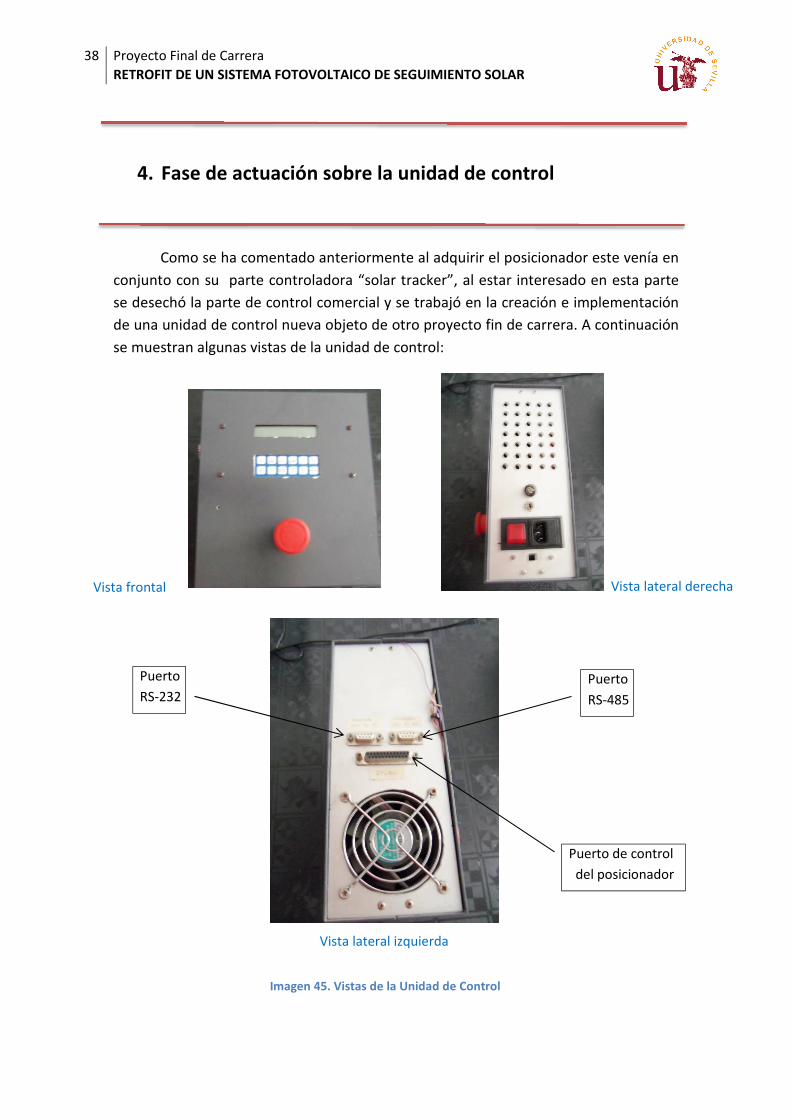
4. Fase de actuación sobre la unidad de control
Como se ha comentado anteriormente al adquirir el posicionador este venía en
conjunto con su parte controladora “solar tracker”, al estar interesado en esta parte
se desechó la parte de control comercial y se trabajó en la creación e implementación
de una unidad de control nueva objeto de otro proyecto fin de carrera. A continuación
se muestran algunas vistas de la unidad de control:
Imagen 45. Vistas de la Unidad de Control
Puerto
RS-232 Puerto
RS-485
Puerto de control
del posicionador
Vista frontal Vista lateral derecha
Vista lateral izquierda

Proyecto Final de Carrera
RETROFIT DE UN SISTEMA FOTOVOLTAICO DE SEGUIMIENTO SOLAR
39
En un primer intento de conectar todos los elementos se observó que no
funcionaba; las variables de los posibles errores eran múltiples. Por lo que se decidió
comenzar a depurarla, saber de qué constaba y se realizó un seguimiento exhaustivo
del cableado interno para saber en qué pin del conector DB 25-pines se tenía que
aplicar tensión para mover los motores del robot posicionador. Se recopiló
información de todos los datasheet de los componentes de las diferentes placas
electrónicas que conforman la unidad de control así como fuente de alimentación
interna y demás (aplicando lo que se puede conocer como ingeniería inversa), para así
poder intentar entender su funcionamiento y poder ir descartando posibles fallos para
llegar al punto de decidir si seguir hacia adelante con la posible reparación u optar por
otra solución.
Para ir teniendo una idea más concreta de lo que constaban las diferentes
partes de la unidad de control se procedió a describir cada una de ellas dividiéndolas
en dos partes, una de control y otra de potencia. Para la parte de control se tiene:
- Tarjeta amplificadora de potencia.
- Tarjeta de aislamiento eléctrico.
- Tarjeta de lectura de encoders.
- Microcontrolador.

40 Proyecto Final de Carrera
RETROFIT DE UN SISTEMA FOTOVOLTAICO DE SEGUIMIENTO SOLAR
- Tarjeta de amplificación de potencia: esta tarjeta se encarga de adaptar las
señales de referencia de los motores que genera el módulo del controlador a
través de los convertidores D/A.
Imagen 46. Placa de adaptación del PK2100 a los servos
Entradas Salidas
Condensador
100 nF Puerta Lógica
SN7400N Relés

Proyecto Final de Carrera
RETROFIT DE UN SISTEMA FOTOVOLTAICO DE SEGUIMIENTO SOLAR
41
- Tarjeta de aislamiento eléctrico: se encarga de aislar eléctricamente el módulo
del microcontrolador del sistema de periféricos externos, también permite
generar la alimentación de las secciones lógicas de todos los componentes.
Dependiendo del tipo de señal el aislamiento eléctrico se realiza de dos formas,
para las señales digitales se emplean acopladores ópticos y para las señales
analógicas se emplean amplificadores de aislamiento.
Imagen 47. Placa Aisladora
Entradas Salidas
Fotoacoplador
PC837
SHARP
Condensadores
220 microF
Convertidor
DC-DC 1W
Aislado
Fotoacoplador
PC827
SHARP
Convertidor
DC-DC 1W
Aislado
Amplificador
de Aislamiento
ISO124P
Regulador de tensión
MC7805CT

42 Proyecto Final de Carrera
RETROFIT DE UN SISTEMA FOTOVOLTAICO DE SEGUIMIENTO SOLAR
- Tarjeta de lectura de encoders: tarjeta diseñada para contar los pulsos
generados por encoders diferenciales con salida a colector abierto. Las señales
generadas por los encoders no está conectada directamente a esta tarjeta sino
a través de la tarjeta de aislamiento eléctrico mediante optoacopladores.
Imagen 48. Tarjeta de Encoders
Oscilador
IQX0-350C
Demultiplexor
74HC138N
Decodificdor
Contador
cuadratura
HCTL2020
Comparador 8-bits
SN74LS688N
Demultiplexor
74HC138N
Octal transparent latch
SN74LS374N

Proyecto Final de Carrera
RETROFIT DE UN SISTEMA FOTOVOLTAICO DE SEGUIMIENTO SOLAR
43
- Microcontrolador PK2100: Sistema donde se basa la unidad de control
completamente programable. Está dotado de varios periféricos, siendo los
principales:
o Puerto de entradas digitales: 7 entradas digitales protegidas.
o Puerto de salidas digitales: 10 salidas de alta intensidad (500 mA, por canal).
o Convertidores D/A: 2 convertidores D/A con resolución de 10 bits y con rango
de 0-120 V.
o Convertidor A/D: convertidor A/D diferencial de alta sensibilidad y 10 bits de
resolución.
o Bus de expansión PCLBus para conexión de dispositivos externos.
o Puerto serie RS-485 y puerto serie RS-232 con líneas RTS/CTS para protocolo
Handshake.
A continuación se muestras diferentes imágenes de la situación actual del
microcontrolador:
Imagen 49. Módulo PK-2100
Vista exterior

44 Proyecto Final de Carrera
RETROFIT DE UN SISTEMA FOTOVOLTAICO DE SEGUIMIENTO SOLAR
Imagen 50. Microcontrolador PK-2100
Para la parte de potencia se tiene:
- PWM (Pulse Width Modulation) Modulación de anchura de pulsos: Se utilizan sobre las
señales generadas por el módulo del microcontrolador, de esta forma se transforman
las señales continuas en trenes de pulsos cuyo período es inferior al tiempo
característico de los motores.
Imagen 51. PWM Servo Azimut y Elevación
Vista interior

Proyecto Final de Carrera
RETROFIT DE UN SISTEMA FOTOVOLTAICO DE SEGUIMIENTO SOLAR
45
En la siguiente imagen que se muestra se puede observar todos los elementos
mencionados anteriormente dentro de su carcasa metálica:
Imagen 52. PWM Ref. Advanced Motion Control 25A8
Imagen 53. Vista general interior Unidad de Control

46 Proyecto Final de Carrera
RETROFIT DE UN SISTEMA FOTOVOLTAICO DE SEGUIMIENTO SOLAR
También se muestra de manera gráfica el esquema de los componentes de la
unidad de control:
Imagen 54. Esquema componentes de la Unidad de Control
Se pudo aclarar mucho más el funcionamiento de la unidad de control y de las
distintas partes de las que consta. En este punto se llegó a la conclusión de que se
debía de realizar un plano de cableado para saber sobre todo que patillas del DB 25
pines se debería de alimentar para intentar mover el robot posicionador (seguidor
solar).
Se anotó las referencias del cableado, el cual debe coincidir con el conector de
la unidad de control.
A continuación se representa el plano del diagrama de conexionado:

47 Proyecto Final de Carrera
RETROFIT DE UN SISTEMA FOTOVOLTAICO DE SEGUIMIENTO SOLAR
Imagen 55. Detalle Conexionado Unidad de Control

Proyecto Final de Carrera
RETROFIT DE UN SISTEMA FOTOVOLTAICO DE SEGUIMIENTO SOLAR 48
Una vez creado el esquema de conexionado de la unidad de control se pudo ver las
conexiones de las distintas placas, así como las correspondientes al pineado del motor,
que era lo que más nos interesaba. Se pudo contar con un cable conectado a un
terminal DB 25 pines hembra para conectarlo con el DB 25 pines macho situado en el
armario. De este cable se utilizó los hilos pertenecientes a la alimentación del motor,
que previamente se pudo determinar con el plano creado.
Estos cables son:
• Azul-Gris (Motor 1);
• Negro-Marrón (Motor 2).
Y con una fuente de alimentación portátil se aplicó 10 V, a la misma vez que se
movía se iba observando con un voltímetro los valores de tensión e intensidad. En el
eje de elevación eran excesivos y se dejó de aplicar, por lo que se pudo observar que el
robot posicionador (seguidor solar) podía moverse, aunque sólo se pudo mover en el
eje azimut y no en el eje de elevación.
También se pudo aprovechar para determinar los terminales en el propio seguidor
correspondiente a los motores. De las 14 conexiones se determinó que:
• 4 – 5: Motor elevación;
• 6 – 7: Motor Azimut.
A estas mismas bornas se conectaron las de la cabeza del Robot Posicionador,
en las siguientes imágenes se puede observar un detalle de la conexión:

Proyecto Final de Carrera
RETROFIT DE UN SISTEMA FOTOVOLTAICO DE SEGUIMIENTO SOLAR
49
Imagen 56. Bornas de cabeza Robot Posicionador
A continuación se muestra cómo quedaría la conexión entre ambas partes,
apoyándonos en el elemento auxiliar comercial suntracker.

50 Proyecto Final de Carrera
RETROFIT DE UN SISTEMA FOTOVOLTAICO DE SEGUIMIENTO SOLAR
Imagen 57. Conexiones entre bornas cabeza robot y suntracker
Por lo que se puede verificar que las pruebas que se realizaron con la f.a.
portátil eran correctas (4 y 5 Elevación) – (6 y 7 Azimut).
Otra de las pruebas que se realizó fue con el suntracker conectado, lo que hace
el robot posicionador es buscar su posición original (ORG) y una vez posicionado seguir
un programa establecido. En unas primeras comprobaciones se observó que no
funcionaba con normalidad y se pudo determinar que uno de los cables en concreto el
que conecta en la borna 1 como COMÚN no estaba bien conectado en uno de sus
extremos por lo que se volvió a conectar correctamente. Con esta forma de actuar se
pudo recoger los datos necesarios.

Proyecto Final de Carrera
RETROFIT DE UN SISTEMA FOTOVOLTAICO DE SEGUIMIENTO SOLAR
51
Al observar la unidad no se apreció que tuviera ningún fusible en mal estado ni
ningún cable mal conectado así como sus distintos bloques que lo conforman, lo que
se apreció es que al conectarla a la red no se encendía el display del microcontrolador
por lo que lo más probable era que el microcontrolador estuviera en mal estado, y
tenía toda la pinta que hubiera sufrido las consecuencias de altas temperaturas.
La primera sensación que se aprecia al abrir la unidad de control, ver imagen
53, es mucha electrónica apilada en un mismo espacio pequeño, con una ventilación
insuficiente tanto por altas temperaturas como por bajas teniéndose que evitar
posibles condensaciones, todo tan perjudicial para la electrónica que se maneja. Se
observó, al disponer de un espacio tan reducido la dificultad de acceder a los distintos
bloques por la cantidad de cable que se trataba para interconectarlos. La estructura
metálica que recubre toda esta electrónica se apreciaba que le dotaba de poca
estanqueidad con las consiguientes posibles entradas de polvo y a lo sumo de agua, ya
que hay que contar que este tipo de instalación se considera semi-industrial.
Antes de tomar ninguna decisión se realizó una comparativa a grandes rasgos
entre el comprar un nuevo microcontrolador, con todo lo que conlleva no solo a
comprar este dispositivo que podría ser una opción bastante económica sino el hecho
que supone el adquirir su herramienta de programación, coste de programación en
cuanto a tiempo de autoaprendizaje del propio lenguaje que maneja y creación del
código desde cero, y con todo ello en el caso que se pudiera llegar a buen término se
seguiría teniendo posibles fuentes de averías en los demás bloques ya que se tratan de
placas de montaje creadas en el departamento. Incluso se tendría que adaptar una
estructura más grande para albergar toda la electrónica con su ventilación adecuada.
Por todo ello se tomó la determinación de utilizar un PLC, ofreciéndonos las
siguientes mejoras a nuestra instalación:
- Mayor fiabilidad/robustez.
- Equipo de propósito general. (Lenguaje que cumple normativa).
- Menor tiempo de desarrollo en el lenguaje (por bloques) en las distintas
modificaciones.
- Menor electrónica asociada en cuanto a las lecturas. Con los diferentes
módulos de entradas, salidas, lecturas rápidas se puede acometer todo lo
necesario para nuestro sistema seguidor.
- Protocolos de comunicaciones con sus estándares.
- Se dota de una unidad de control con mayor IP. Aunque en la instalación que
nos acontece va ubicado en el interior del armario eléctrico este tipo de
instalaciones comerciales van situados a pie de seguidor solar, evitando tiradas

52 Proyecto Final de Carrera
RETROFIT DE UN SISTEMA FOTOVOLTAICO DE SEGUIMIENTO SOLAR
grandes de cableado de los distintos sensores y aguantando condiciones
climatológicas adversas.
Se puede concluir que hay que cambiar la parte de control por otro equipo de
control en concreto un autómata programable y para la parte de potencia
(amplificadores de los motores, estos equipos funcionan y sí se conservan.
4.1. PLC OMRON
Se optó por decidir utilizar un PLC para gobernar la parte de control del sistema.
Como primera elección se decidió utilizar un PLC de OMRON, ya que se
aprovecharía el autómata usado por otro proyecto (también de posicionamiento).
Como ventaja se puede decir que se podría “reutilizar” parte del programa que ya se
usó en el otro proyecto, pero como desventaja se puede nombrar que no tiene
entradas digitales rápidas, aunque se tendría que comprobar si las que tiene permite la
lectura de los encoders, no tiene salidas analógicas, aunque puede que no hagan falta
teniendo en cuenta que los motores llevan reductoras. A continuación se muestra una
imagen del PLC de OMRON a utilizar.
Imagen 58. PLC serie CJ1M de OMRON.
Entre sus características destaca su configuración rápida y sencilla así como su
diseño muy compacto (96x65mm).
Se continuó las pruebas con el plc de Omron:

Proyecto Final de Carrera
RETROFIT DE UN SISTEMA FOTOVOLTAICO DE SEGUIMIENTO SOLAR
53
- Se instaló el software denominado “CX-Programmer”.
- Se procedió a la lectura de varios proyectos “Dimecosol: Diseño e
implementación de Estrategia de Control para Seguidor Solar”.
- Se procedió a la realización de un cable de comunicaciones RS-232 para
comunicarse con el autómata y a continuación otro cable para comunicarse vía
Ethernet.
- Una vez que se manejó el programa se probó la posibilidad de contar los pulsos
con la tarjeta actual para llegar a la determinación de comprar o no la tarjeta
adecuada para el contaje de lectura rápida en base a las medidas tomadas.
Se procede a detallar con más detenimiento lo anteriormente comentado.
4.1.1. PLC CJ1M
A continuación se muestran las distintas partes de la que consta el PLC utilizado.
• CJ1M-PA202: fuente de alimentación interna del autómata.
• CJ1M-CPU13ETH: CPU del autómata.
• CJ1W-ID211: tarjeta de 16 entradas digitales.
• CJ1W-OC201: tarjeta de 8 salidas digitales.
• CJ1W-AD041-V1: tarjeta de entradas analógicas.
Imagen 59. Partes del PLC
CJ1M-PA202 CJ1M-CPU13ETH CJ1W-ID211 CJ1W-OC201 CJ1W-AD041-V1

54 Proyecto Final de Carrera
RETROFIT DE UN SISTEMA FOTOVOLTAICO DE SEGUIMIENTO SOLAR
CJM-PA202: fuente de alimentación.
- Rango de entrada: 85 a 264 Vca / 47 a 63 Hz
- Consumo: 50 VA máx.
- Capacidad de salida a 5 Vcc: 2.8 A
- Capacidad de salida a 24 Vcc: 0.4 A
- Potencia máx. de salida: 14 W
Interface
Imagen 60. Interface externa CJM-PA202

Proyecto Final de Carrera
RETROFIT DE UN SISTEMA FOTOVOLTAICO DE SEGUIMIENTO SOLAR
55
Dimensiones
Imagen 61. Dimensiones CJM-PA202
CJ1M-CPU13ETH: modelo de la CPU del autómata.
- Máximo de puntos de E/S digitales: 640
- Capacidad de programa: 20 k
- Capacidad de memoria de datos: 32 k
- Velocidad de ejecución: 100 ns
- Máx. nº de unidades de E/S: 19
- Consumo de 5V: 950 mA
- Funciones incorporadas: Puerto Ethernet 100 Base-Tx
Interface
Imagen 62. Interface externo CJ1M-CPU13ETH

56 Proyecto Final de Carrera
RETROFIT DE UN SISTEMA FOTOVOLTAICO DE SEGUIMIENTO SOLAR
Dimensiones
Imagen 63. Dimensiones CJ1M-CPU13ETH
CJ1W-ID211: tarjeta de 16 entradas digitales.
- Puntos: 16
- Tipo: Entrada de c.c.
- Tensión nominal: 24 V.c.c.
- Corriente nominal: 7mA
- Tipo de conexión: M3
Conexión externa
Imagen 65. Conexión externa CJ1W-ID211
Imagen 64. Terminales M3

Proyecto Final de Carrera
RETROFIT DE UN SISTEMA FOTOVOLTAICO DE SEGUIMIENTO SOLAR
57
Interface
Imagen 66. Interface externo CJ1W-ID211
Dimensiones
Imagen 67. Dimensiones CJ1W-ID211

58 Proyecto Final de Carrera
RETROFIT DE UN SISTEMA FOTOVOLTAICO DE SEGUIMIENTO SOLAR
CJ1W-OC201: tarjeta de 8 salidas digitales.
- Puntos: 8
- Tipo: Salida de relé.
- Tensión nominal: 250 Vca.
- Corriente nominal: 2 A.
- Tipo de conexión: M3
Conexión externa
Imagen 68. Conexión externa CJ1W-OC201
Interface
Imagen 69. Interface externa CJ1W-OC201

Proyecto Final de Carrera
RETROFIT DE UN SISTEMA FOTOVOLTAICO DE SEGUIMIENTO SOLAR
59
Dimensiones
Imagen 70. Dimensiones CJ1W-OC201
CJ1W-AD041-V1: tarjeta de entradas analógicas.
- Puntos: 4
- Tipo: Entrada analógica
- Rangos: 0-5V / 0-10V / -10-10V / 1-5V / 4-20mA
- Resolución: 1/8.000
- Precisión: V: 0.2% / I: 0.4%
- Tiempo de conversión: 250 µ/punto
- Observaciones: Ajuste de offset/ganancia, retención del valor de pico, media
móvil, alarmas.
- Tipo de conexión: M3.

60 Proyecto Final de Carrera
RETROFIT DE UN SISTEMA FOTOVOLTAICO DE SEGUIMIENTO SOLAR
Disposición de los terminales
Imagen 71. Disposición de los terminales CJ1W-AD041-V1
Componentes
Imagen 72. Componentes CJ1W-AD041-V1

Proyecto Final de Carrera
RETROFIT DE UN SISTEMA FOTOVOLTAICO DE SEGUIMIENTO SOLAR
61
Dimensiones
Imagen 73. Dimensiones CJ1W-AD041-V1
4.1.2. Instalación CX-Programmer V5.0.
Se procedió a instalar el software CX-Programmer V5.0, también nos puede valer
una versión superior. En el propio proceso de instalación se procede también a instalar
las librerías y el CX-Server necesario para las comunicaciones, se recomienda instalar
todo.
Imagen 74. Logo CX-Programmer al iniciar.
4.1.3. Cables para conexión
En este paso se procede a explicar la construcción del cable para los distintos
protocolos de conexión, uno para conexión RS-232C (SYSMAC WAY) y otro para
conexión ETHERNET 10/100 MBits.
Cable serie RS-232C
o 1 ud conector DB9-pines macho.
o 1 ud conector DB9-pines hembra.
o 1-2 m cable 5-6 hilos.

62 Proyecto Final de Carrera
RETROFIT DE UN SISTEMA FOTOVOLTAICO DE SEGUIMIENTO SOLAR
Imagen 75. DB9-Pines macho.
Imagen 76. DB9-Pines hembra.
En la siguiente imagen se puede observar perfectamente las conexiones a
realizar entre ambos entremos.
Imagen 77. Conexión cableada entre PLC-PC.
Cable ETHERNET:
o 2 uds RJ-45.
o 2-3 m cable UTP 4 pares Cat 5-5e.
En este caso ambos extremos se corresponden con conectores RJ-45 y el
conexionado entre ambos extremos tiene que corresponderse como se observa en la
imagen 88 referente a la conexión de cable cruzado.

Proyecto Final de Carrera
RETROFIT DE UN SISTEMA FOTOVOLTAICO DE SEGUIMIENTO SOLAR
63
Imagen 78. Conexión cable cruzado.
Imagen 79. Unidad de RJ-45.
4.1.4. Crear nuevo proyecto con CX-Programmer.
Una vez que se tiene instalado el CX-Programmer y los cables para las conexiones
SYSMAC WAY y ETHERNET 10/100 Mbits, se realizó un programa básico en ladder, con
el fin de probar que se ha realizado bien las conexiones del pineado y se puede
transferir al PLC la programación realizada, para ello:
- Doble click en el icono del programa donde se encuentre
instalado.
- Se crea proyecto proyecto nuevo.
Imagen 80. Detalle icono nuevo proyecto.

64 Proyecto Final de Carrera
RETROFIT DE UN SISTEMA FOTOVOLTAICO DE SEGUIMIENTO SOLAR
- Se nombra el proyecto nuevo y se elige nuestra CPU y el tipo de
comunicaciones a establecer.
Imagen 81. Definiendo parámetros.
- Se define el tipo de CPU dentro del tipo de dispositivo en configurar.
Imagen 82. Detalle icono configurar tipo de dispositivo.
Imagen 83. Pasos para definir tipo de CPU.

Proyecto Final de Carrera
RETROFIT DE UN SISTEMA FOTOVOLTAICO DE SEGUIMIENTO SOLAR
65
- Se define las propiedades de tipo de red en configurar (puerto, velocidad en
baudios, bits de datos, paridad, datos de parada (COMX, 9600, 7, Par, 2).
Imagen 84. Detalle icono configurar tipo de red.
Imagen 85. Configurando parámetros de conexión.
- Esos mismos datos tiene que coincidir en los parámetros del PC; para Windows
7:
Inicio -> Botón derecho en Equipo -> Propiedades -> Administrador de dispositivos
-> Puertos -> Doble click puerto elegido -> Configuración del puerto -> (9600, 7,
Par, 2, Ninguno).
Imagen 86. Pasos a seguir para definir los parámetros de conexión del PC.

66 Proyecto Final de Carrera
RETROFIT DE UN SISTEMA FOTOVOLTAICO DE SEGUIMIENTO SOLAR
4.1.5. Definiendo Tabla de E/S.
Una vez realizado todo lo anterior se vuelve al programa CX-Programmer.
Doble click en Tabla de E/S -> Desplegar +Bastidor Principal -> Botón derecho en 00
[0000] Hueco Vacio -> Unidad SIO CPU CS/CJ -> Unidad Ethernet (ET).
Imagen 87. Agregando módulos a la tabla de E/S.
4.1.6. Definiendo el bastidor principal.
Así hasta completar todos los módulo/tarjetas que componen nuestro PLC.
Imagen 88. Detalle bastidor principal con los módulos insertados.

Proyecto Final de Carrera
RETROFIT DE UN SISTEMA FOTOVOLTAICO DE SEGUIMIENTO SOLAR
67
4.1.7. Compilando y conectando.
A continuación se compila , y se observa los posibles errores de código
así como las advertencias posibles, una vez subsanadas, se presiona Trabajar Online
.
(Conectar ambos lados del cable serie PC-PLC).
Imagen 89. Detalle de pantallazo para confirmar la conexión entre PLC-PC.
4.1.8. Transfiriendo información desde el PC al PLC.
Botón derecho en el nombre el PLC (lado izquierdo del CX-Programmer) ->
Transferir -> A PLC.
Imagen 90. Pasos a seguir para transferir datos al PLC.
Es aconsejable la primera vez que se haga una transferencia al PLC de marcar todas
las opciones y ya para las siguientes sólo las que nos convengan o hayan sufrido
cambios posteriores.

68 Proyecto Final de Carrera
RETROFIT DE UN SISTEMA FOTOVOLTAICO DE SEGUIMIENTO SOLAR
Imagen 91. Detalle de marcado a incluir en la 1ª transferencia hacia el PLC.
Imagen 93. Detalle pantallazo antes de transferir.
Imagen 94. Detalle transferencia finalizada.
Imagen 92. .Detalle pantallazo cambio de modo de fto. necesario para transferir

Proyecto Final de Carrera
RETROFIT DE UN SISTEMA FOTOVOLTAICO DE SEGUIMIENTO SOLAR
69
Imagen 95. Detalle % uso de memoria tras la transferencia de datos.
Imagen 96. Detalle cambio modo funcionamiento al que tenía antes de la transferencia.
4.1.9. Monitorizando y modos de funcionamiento.
Una vez que se le ha transferido toda la configuración preestablecida así como la
programación realizada, se debería de observar el gráfico de una apariencia
aproximada como la que se aprecia en la imagen siguiente, aparece en la parte
izquierda Registro de error, el cual nos dirá si hay algún error que subsanar. Después se
aplica Alternar monitorización de PLC , aparecerá unas líneas verdes donde se
deduce el seguimiento de la monitorización del propio programa. Hay 3 maneras de
funcionamiento: Modo RUN , Modo Monitor o Modo Programa , se puede
optar de una opción a otra dependiendo si se quiere realizar algún cambio en modo
Online, o si quiere cargar o no de nuevo alguna modificación al PLC.
Imagen 97. Detalle pasos a seguir para monitorización y modos de funcionamiento.

70 Proyecto Final de Carrera
RETROFIT DE UN SISTEMA FOTOVOLTAICO DE SEGUIMIENTO SOLAR
4.1.10. Conexión Ethernet.
Llegado a este punto, necesario para ahora poder establecer conexión Ethernet, el
cual se consigue ganar sobre todo velocidad así como una conexión mucho más
estable.
En modo offline -> Doble click en el nombre el PLC (lado izquierdo del CX-Programmer)
-> Tipo de Red Ethernet -> Configurar -> Controlador -> Dirección IP (por ej.:
172.16.99.1).
Como puede verse en el paso número 7 de la imagen, en este caso “15”, se va a
corresponder a la terminación de la dirección IP que se tiene que configurar, a
continuación en Conexión de área local del PC (por ej.: 172.16.99.15, 255.255.255.0).
4.1.11. IP del PC.
En Windows7, Inicio -> Panel de control -> Redes e Internet -> Centro de Redes y
recursos compartidos -> Cambiar configuración del adaptador -> Botón derecho
Conexión de área local -> Propiedades ->Doble click Protocolo de internet versión 4
(TCP/IPv4) -> Propiedades -> Usar la siguiente dirección IP -> Aceptar.
Imagen 98. Detalle configuración Ethernet en PLC.

Proyecto Final de Carrera
RETROFIT DE UN SISTEMA FOTOVOLTAICO DE SEGUIMIENTO SOLAR
71
Imagen 99. Detalle configuración Ethernet en PC.
Una vez realizados los pasos 9 y 10 se puede volver al paso 7.
4.1.12. Enviar y recibir datos a través del puerto RS-232C.
Para realizar esta prueba se tiene que tener todo lo anterior verificado que
funciona y como se va a proceder a probar en el mismo PC, se debe de tener ambas
conexiones (SYSMAC WAY y ETHERNET) a la vez.
Se van a utilizar las funciones @TXD (función transmitir) y @RXD (función recibir).
Antes de nada se tiene que configurar el puerto de la CPU ya que es con el que se va a
tratar la lectura y escritura de la memoria interna.
Se ha creado un programa básico denominado “Transmitir y Recibir.cxp”, de donde
se va a realizar la siguiente explicación.
Se abre el programa “Transmitir y Recibir.cxp” o también se puede generar uno
nuevo desde el principio, con los pasos anteriores, pero se realiza la conexión con el
autómata con Ethernet.
En modo offline, doble click en Selecciones -> Puerto de Host link -> Modo ->
RS232C.

72 Proyecto Final de Carrera
RETROFIT DE UN SISTEMA FOTOVOLTAICO DE SEGUIMIENTO SOLAR
Imagen 100. Pasos a seguir para poder establecer conexión RS232C con CPU del PLC
4.1.13. Hyperterminal.
Se usará el programa Hyperterminal para poder enviar desde él y recibir el PLC y al
contrario también. Se conectará vía Ethernet PC-PLC y vía serie al hyperterminal (PC)-
PLC, quedando una conexión como sigue:
Imagen 101. Detalle gráfico de conexión PLC-PC y PC-PLC con Hyperterminal
4.1.14. @TXD & @RXD.
Se utiliza la función @TXD para transmitir información por el puerto RS232C, se
tiene que escribir en la dirección de memoria asignada para que se pueda enviar así
como definir la cantidad de bits máximos. Pasa lo mismo con @RXD, se recibe, en este
caso, desde el hyperterminal, y se almacenará en la dirección de memoria
preestablecida, así como la cantidad de bits a recibir.

Proyecto Final de Carrera
RETROFIT DE UN SISTEMA FOTOVOLTAICO DE SEGUIMIENTO SOLAR
73
Imagen 102. Detalle ejemplo para transmitir y recibir desde CX-Programmer
En este caso concreto se podrá transmitir hasta un máximo de 20 bits de
información empezando desde la dirección D1000, y se podrá recibir también 20 bits
máximos empezando en la posición de la memoria D1600.
Al ser un ejemplo básico se tendrá que ir forzando a ON los contactos I0.00 e
I0.01, en el caso que se requiera para ir enviando o recibiendo en cada activación, por
ejemplo:
- Me voy al espacio de memoria D1000 y escribo: “Envio de trama de datos”,
fuerzo a ON I0.00 (botón derecho encima del contacto I0.00 -> Forzar -> ON) y
aparece lo escrito en el Hyperterminal. Fuerzo a OFF I0.00 (botón derecho
encima del contacto I0.00 -> Forzar -> OFF).
Imagen 103. Detalle para forzar el contacto a ON necesario para transferir datos desde la memoria de la CPU del PLC al hyperterminal

74 Proyecto Final de Carrera
RETROFIT DE UN SISTEMA FOTOVOLTAICO DE SEGUIMIENTO SOLAR
I0.00 Forzado a ON:
Imagen 104. Detalle gráfico de cómo queda el entorno al forzar
Accediendo a la memoria de datos:
Doble click en 1 Memoria -> 2 Poner texto en formato ASCII -> 3 Monitorizar -> 4
Indicar la dirección inicial -> 5 Escribir los datos a transmitir.
Imagen 105. Pasos a seguir para preparar el envío de datos
Imagen 106. Vista del envío y resultado de la recepción desde el hyperterminal
- Ahora desde el Hyperterminal escribo, por ejemplo: “diego aragon”, fuerzo a
ON el I0.01 y aparece en la dirección D1600 lo escrito. Fuerzo a OFF I0.01.

Proyecto Final de Carrera
RETROFIT DE UN SISTEMA FOTOVOLTAICO DE SEGUIMIENTO SOLAR
75
Imagen 107. Vista ahora del envío desde hyperterminal y recepción en memoria CPU
*Se puede obtener mucha más información acerca de estas instrucciones así como
muchas más en los manuales anexados.
4.1.15. LabView.
También se realizaron pruebas de emisión y recepción con el programa de
visualización LabView.
En este caso se instaló la versión 2010.
Imagen 108. Pantalla de inicio de LabView 2010

76 Proyecto Final de Carrera
RETROFIT DE UN SISTEMA FOTOVOLTAICO DE SEGUIMIENTO SOLAR
Se utilizó un programa básico que trae el propio programa de Labview como
ejemplo, denominado “Serial Write and Read”, que como su propio nombre indica
sirve para leer y escribir desde el puerto serie.
A continuación se muestra una imagen de la apariencia del programa:
Imagen 109. Programa Serial Write and Read

Proyecto Final de Carrera
RETROFIT DE UN SISTEMA FOTOVOLTAICO DE SEGUIMIENTO SOLAR
77
Este caso sería similar al estudiado anteriormente lo único que se sustituirá el
hyperterminal por el programa LabView para establecer comunicación vía serie y
Ethernet, que es el objetivo final.
Imagen 110. Detalle gráfico de conexión PLC-PC y PC-PLC con LabView
Se utilizan las mismas funciones y los mismos registros de memorias, así como las
misas órdenes para realizar las pruebas correctas de transferencia de datos pero en
este caso desde el PLC al programa LabView2010.
Imagen 111. Envío de datos desde el PLC al PC (LabView)

78 Proyecto Final de Carrera
RETROFIT DE UN SISTEMA FOTOVOLTAICO DE SEGUIMIENTO SOLAR
Imagen 112. Envío de datos desde el PC (LabView) al PLC
Una vez desarrollados todos los pasos descritos anteriormente se está en
disposición de realizar las pruebas pertinentes para el conteo de los pulsos con la
tarjeta actual y así saber si nos sirve o no.
Se realizaron distintas pruebas para poder determinar la frecuencia de los pulsos
de los encoder del seguidor, llegando a la conclusión que el módulo de entrada digital
(CJ1W-ID211) es a 45 Hz y a 1.9 V cuando puede apreciarse un conteo razonable. Se
realizaron dos esquemas tipos para leer la fase A de azimut, uno sin divisor de tensión
y otro con divisor donde a través de una resistencia variable se pudo ajustar a 1.9 V
una lectura de frecuencia más aceptable para el módulo de entrada digital. La tarjeta
digital no admite una frecuencia alta, si la plataforma se debe mover más rápido para
alcanzar una posición de defensa o simplemente para hacer un posicionamiento por
no estar orientada bien, se perderían pulsos del encoder y la posicíón.
Para poder desarrollar estas pruebas también se tuvo que realizar una búsqueda
de información del tipo de encoder que dispone nuestro posicionador. Primero se
observó el tipo de conector que tiene el suntracker en su parte trasera:

Proyecto Final de Carrera
RETROFIT DE UN SISTEMA FOTOVOLTAICO DE SEGUIMIENTO SOLAR
79
Open Collector (O.C.) NPN
Circuito de salida Driver ULN 2003 o equivalente
Capacidad de carga 40 mA por canal
Longitud de cable admisible 50 m (Vcc = 24 Vdc)
Resistencia de carga aconsejable RL = 1,8K (Vcc = 24 Vdc)
Nivel de señal "Low" VOL < 2V (Vcc = 24 Vdc)
Nivel de señal "High" VOH > 22V (Vcc = 24 Vdc)
Alimentación 11....30 Vdc
Ondulación máxima 300 m V Vcc
Protección contra cortocircuito No permanente
Frecuencia máx. standard 50 kHz - 100 kHz
Imagen 113. Detalle conector tipo M12 8P denominado MOTOR/PULS
Imagen 114. Encoder NPN Open Collector
Imagen 115. Esquema típico Encoder NPN O.C.

80 Proyecto Final de Carrera
RETROFIT DE UN SISTEMA FOTOVOLTAICO DE SEGUIMIENTO SOLAR
Se muestra a continuación la correspondencia de colores de los cables con los
pines de cada conector (Suntracker, DB-9, DB-25):
Imagen 116. Correspondencia colores cables – pines
Seguidamente se procede a mostrar esquemáticamente las conexiones de los
distintos elementos que intervienen para realizar las pruebas de lectura de los pulsos
del encoder para determinar si la tarjeta del PLC lee correctamente las entradas
rápidas.

Proyecto Final de Carrera
RETROFIT DE UN SISTEMA FOTOVOLTAICO DE SEGUIMIENTO SOLAR
81
- Prueba sin divisor:
Imagen 117. Esquema de la prueba sin divisor de tensión
- Prueba con divisor:
Imagen 118. Esquema de la prueba con divisor de tensión
En la imagen siguiente se recoge en una tabla origen y destino, así como color,
de cada cable utilizados en cada una de las pruebas anteriores:

82 Proyecto Final de Carrera
RETROFIT DE UN SISTEMA FOTOVOLTAICO DE SEGUIMIENTO SOLAR
Herramientas y equipos utilizados:
Imagen 120. Polímetro
Imagen 121. Fuente de alimentación 24 Vac
Imagen 123. Fuente alimentación variable
Imagen 119. Pruebas Azimut y Elevación
Imagen 122. Encoder para realizar pruebas manuales de incrto. y decrto. de pulsos

Proyecto Final de Carrera
RETROFIT DE UN SISTEMA FOTOVOLTAICO DE SEGUIMIENTO SOLAR
83
En estas dos imágenes siguientes se puede apreciar los equipos cableados para
las distintas pruebas:
En el CX-Programmer se utilizó un temporizador de alta velocidad TIMH donde
iba a estar contando cada segundo, seguidamente con un contador reversible CNTR,
para poder observar el incremento de la lectura (de 0 hacia arriba), se le programa una
entrada que es la propia de los pulsos de la Fase A (cable verde) en la entrada In0.2, y
se le programa un reseteo del temporizador creado anteriormente, por lo que cada
segundo se resetea nuestro contador y así se puede ver los pulsos que se genera cada
segundo. A continuación se observa una captura de pantalla:
Imagen 125. Temporizador de alta velocidad (TIMH) con contador reversible (CNTR)
Imagen 124. Diferentes imágenes de las conexiones para las pruebas

84 Proyecto Final de Carrera
RETROFIT DE UN SISTEMA FOTOVOLTAICO DE SEGUIMIENTO SOLAR
Llegado a este punto se observó la necesidad de disponer de un módulo de
contaje para lectura rápida. Se preguntó precio para adquirir uno de la serie OMRON
siendo el coste de este:
Código Descripción Cantidad Precio/Und Importe
315605 Módulo contador alta velocidad.2 Ent.500KHz CJ1W-CT021
1,00 542,50€ 542,50€
Y también se preguntó precio a Schneider Electric por un autómata nuevo con
lectura rápida:
Referencia Descripción/Contenido Importe
CMDM238AVAS
Autómata Programable Modicon M238 compacto, alimentado a 24 Vcc, 10 entradas digitales (4fast), 4 salidas digitales a transistor y 6 a relé, 4 entradas analógicas (V-I), 2 salidas analógicas (V-I) puerto de comunicación Modbus y CANOpen, cable de programación USB y software SOMachine.
540,00€
Se puede observar sale más económico el adquirir el M238 ya que se adquiere
un PLC completo, CPU más actual, módulos de entras y salidas, cable software y sin en
cambio por el mismo precio se adquiría sólo un módulo de contaje rápido teniendo
una CPU más antigua.
En esta misma fase de actuación se describen también los trabajos realizados
en cuanto al saneado y aprovechamiento del cableado existente.
A continuación se muestra en modo esquemático el cableado que se dispone
en el laboratorio y se muestra algunas imágenes del estado actual del propio cableado:

Proyecto Final de Carrera
RETROFIT DE UN SISTEMA FOTOVOLTAICO DE SEGUIMIENTO SOLAR
85
Imagen 126. Esquema de cableado laboratorio-armario-campo
Imagen 127. Conversor RS485 – RS232

86 Proyecto Final de Carrera
RETROFIT DE UN SISTEMA FOTOVOLTAICO DE SEGUIMIENTO SOLAR
Imagen 128. Cableado actual en laboratorio.
De todo el cableado y componentes existentes se aprovecha parte de él
quedando un resultado final como se muestra en el detalle del pineado del cable para
poder enviar y recibir datos desde el PLC, situado en el armario, hasta el PC, ubicado
en el laboratorio, se aprovecha tanto los convertidores RS485-RS232, así como el cable
existente, a continuación el detalle:

Proyecto Final de Carrera
RETROFIT DE UN SISTEMA FOTOVOLTAICO DE SEGUIMIENTO SOLAR
87
Imagen 129. Detalle cableado PLC - PC
Se comprueba en la prueba final (PLC en el armario) y desde el laboratorio que
enviaba y recibía perfectamente.
Se concluye que los conversores RS232/RS-485 con sus fuentes de alimentación
también se prueban y se conservan.
4.2. PLC SCHNEIDER ELECTRIC M238
Se procedió a la instalación del software ‘SoMachine 3.1.’ y a la construcción
del cable para poder realizar el envío y recepción de datos entre PLC y PC. En la
siguiente imagen se puede observar el logo del software utilizado de Schneider
Electric.

88 Proyecto Final de Carrera
RETROFIT DE UN SISTEMA FOTOVOLTAICO DE SEGUIMIENTO SOLAR
Imagen 130. Logo software SoMachine V.3.1
En la siguiente imagen se puede apreciar la conexión que se tiene que realizar
para fabricarnos el cable necesario para el correcto envío y la correcta recepción de
datos, también se tiene la opción de adquirir el cable ya construido, el cual se muestra
en la otra imagen, y cuya referencia comercial es “TCSMCN3M4F3C2”:
Imagen 131. Cable RJ45-RS232 para PLC-PC

Proyecto Final de Carrera
RETROFIT DE UN SISTEMA FOTOVOLTAICO DE SEGUIMIENTO SOLAR
89
Se dispone del PLC montado en un carril DIN con los siguientes elementos:
- Fuente 24V
- CPU M238
- Tarjeta analógica 4 entradas / 2 salidas
- Enchufe de red
- Cable USB
- Fusible de 1 A.
- Documentos de la CPU y de la tarjeta analógica
La tarjeta analógica, la CPU y los negativos de las entradas digitales se han dejado
conectados en alimentación.
Imagen 132. Elementos del M238 de Schneider Electric

90 Proyecto Final de Carrera
RETROFIT DE UN SISTEMA FOTOVOLTAICO DE SEGUIMIENTO SOLAR
A continuación se muestra un esquema del sistema completo utilizado en la
instalación:
Imagen 133. Esquema del sistema completo utilizado

Proyecto Final de Carrera
RETROFIT DE UN SISTEMA FOTOVOLTAICO DE SEGUIMIENTO SOLAR
91
5. Fase de actuación sobre elementos auxiliares
En esta fase se evaluó los sensores auxiliares de irradiancia, se describen sus
propiedades:
- Sensor de irradiancia Pyranometer (LI200 PY-31396): sensor que le sirve al
controlador de ir tomando los valores de irradiancia e ir posicionándose a
través de ellos. Este sensor se encuentra a escasos metros del robot
posicionador, en el armario se encuentra su conversor para poder obtener los
valores digitales.
Imagen 134. Sensor de irradiancia

92 Proyecto Final de Carrera
RETROFIT DE UN SISTEMA FOTOVOLTAICO DE SEGUIMIENTO SOLAR
En el armario también se puede observar un transmisor básico de aislamiento
para las señales unipolares mA / V que se recogen del sensor de irradiancia. Este
dispositivo consta con selección de rango para su calibrado, en concreto se ha utilizado
el IsoPAQ-30P.
Imagen 135. IsoPAQ-30P
Imagen 136. Sensor de Irradiancia. Pyranometer (LI200 PY-31396)

Proyecto Final de Carrera
RETROFIT DE UN SISTEMA FOTOVOLTAICO DE SEGUIMIENTO SOLAR
93
Se puede concluir que estos equipos funcionan y se conservarán.
Para esta última fase se realizó una propuesta de mejora que consiste en un nuevo
sensor solar que existe en el mercado a sustituir con el sensor nuestro de irradiancia
actual. Este sensor está desarrollado por la empresa SOLAR MEMS Technologies, que
ya se ha utilizado en aplicaciones comerciales reales así como en otros proyectos
finales de carreras de otros compañeros.
Este sensor solar se basa en la tecnología MEMS (Micro-electro-mechanical-
system). Solar MEMS dispone de cuatro familias de sensores para su uso en diferentes
sistemas de seguimiento solar como fotovoltaico, CPV, HCPV, cilindro parabólico,
Stirling…y en cualquier sistema de seguimiento de 1 ó 2 ejes. Estos sensores solares
son de alta precisión y son ideales para sistemas de seguimiento solar.
A continuación se observan las cuatro familias disponibles:
5.1. Sensor solar ISS-AX (Analógico)
El sensor solar ISS-AX proporciona la medida del vector solar incidente. Este sensor
ha sido diseñado con tecnología MEMS para lograr la máxima integración y el menos
coste. El sensor proporciona la medida del ángulo incidente del sol mediante 4 señales
analógicas y un cálculo matemático. En la fig. 137 se puede ver una imagen del sensor
solar. La alta precisión alcanzada es debido a la geometría y diseño del mismo. Sus
características lo hacen ideal para su uso en sistemas de seguimiento de precisión en
dos ejes.
Imagen 137. Sensor Solar ISS-AX

94 Proyecto Final de Carrera
RETROFIT DE UN SISTEMA FOTOVOLTAICO DE SEGUIMIENTO SOLAR
Versiones del sensor solar ISS-AX:
Características ISS-A60 ISS-A25 ISS-A15
Campo de visión 120x120 50x50 30x30
Precisión sin calibración <3 <2 <1
Precisión calibrado a 0° <0,1 <0,07 <0,04
Ver fig. 138.
Imagen 138. Vistas Sensor solar ISS-AX
Características técnicas:
Tipo de sensor: 2 ejes.
Alimentación: 5÷12 V.
Consumo: 11 mA (corriente).
Salidas analógicas: 4 señales 0-4.5 V. Voltaje de cada cuadrante. 4-cuadrante
microsensor.
Temperatura: de -40° a 85°.
Protección: Polaridad inversa.
IP65.
La precisión puede ser incrementada, en más de un orden, mediante la
calibración de la posición del cero después de la instalación.

Proyecto Final de Carrera
RETROFIT DE UN SISTEMA FOTOVOLTAICO DE SEGUIMIENTO SOLAR
95
5.2. Sensor solar ISS-DX (Digital)
El sensor solar ISS-DX proporciona la posición del sol con una alta precisión. Ha sido
diseñado con tecnología MEMS, lo que permite obtener un sensor altamente
integrado con un bajo coste. El sensor ISS-DX mide el ángulo de incidencia de un rayo
solar en dos ejes ortogonales y la radiación del sol. La alta sensibilidad alcanzada se
basa en el diseño de la geometría y en el proceso de calibración final. Las
características de este sensor lo hace una herramienta imprescindible para su uso en
sistemas de seguimiento de alta precisión. En la siguiente fig. 139 se observa el sensor
solar DX.
Imagen 139. Sensor Solar DX
Versiones del sensor solar ISS-DX:
Características ISS-D60 ISS-D25 ISS-D15 ISS-D5
Campo de visión 120x120 50x50 30x30 10x10
Precisión campo de visión <0,4 <0,3 <0,2 <0.1
Precisión sobre 0° <0,06 <0,04 <0,02 <0,005
Ver fig. 140.

96 Proyecto Final de Carrera
RETROFIT DE UN SISTEMA FOTOVOLTAICO DE SEGUIMIENTO SOLAR
Imagen 140. Vistas Sensor Solar ISS-DX
Características técnicas:
Tipo de sensor: 2 ejes.
Alimentación: 5÷12 V.
Consumo: 33 mA (corriente).
Comunicación: RS-485
Máximo 15 sensores/bus
0,05 s de respuesta.
Salida de datos: Ángulos X-Y (filtro incluido)
Radiación solar directa
Temperatura: de -40° a 85°.
Protección: Polaridad inversa.
IP65.

Proyecto Final de Carrera
RETROFIT DE UN SISTEMA FOTOVOLTAICO DE SEGUIMIENTO SOLAR
97
5.3. Sensor solar ISS-CYPA (Cilindro Parabólico)
El sensor solar ISS-CYPA permite ISS-CYPA permite la medición del ángulo de
incidencia de un rayo solar, proporcionando sus ángulos de proyección en los dos ejes
ortogonales de referencia, lo que lo hace ideal para su uso en sistemas de seguimiento
de 1 eje. El sensor ISS-CYPA proporciona la medida del ángulo incidente del sol en dos
ejes, pero con una elevada precisión en un eje, ideal para su aplicación en sistemas
cilindro parabólico y sistemas de seguimiento de 1 eje. En la fig. 141 se puede apreciar
una imagen del dispositivo y en la fig. 142 se puede ver las características técnicas. La
alta precisión está basada en el diseño geométrico y en la calibración final del sensor.
Imagen 141. Sensor Solar ISS-CYPA
Características técnicas:
Tipo de sensor: 2 ejes.
Campo de visión: 80x20° (ejes cypa)
Precisión campo de visión: <0,4°
Precisión en eje-cypa : <0,02°
Alimentación: 5÷12 V.
Consumo: 33 mA (corriente).
Comunicación: RS-485
Máximo 15 sensores/bus
0,05 s de respuesta.
Salida de datos: Ángulos X-Y (filtro incluido)
Radiación solar directa
Temperatura: de -40° a 85°.
Protección: Polaridad inversa.
IP65.

98 Proyecto Final de Carrera
RETROFIT DE UN SISTEMA FOTOVOLTAICO DE SEGUIMIENTO SOLAR
Imagen 142. Vistas Sensor Solar ISS-CYPA
5.4. Sensor solar NANO-ISS60 (NANO)
El sensor NANO-ISS60 permite la medida de la proyección del vector solar
incidente, proporcionando sus ángulos de proyección en los dos ejes ortogonales
de referencia, aplicando simples cálculos matemáticos. La fóvea es función de la
geometría del sensor. En la fig. 143 se aprecia el sensor solar. Su diseño compacto,
fácil integración y reducido consumo, lo hacen ideal para sistemas de seguimiento
en energía renovable o sistemas que precisen conocer la posición del sol a un bajo
coste. El sensor NANO-ISS60 puede ser suministrado con dos formatos: uno sobre
PCB y otro sobre PCB con conector (NANO-ISS60-c). En la fig. 144 se observa las
características técnicas del sensor.
Imagen 143. Sensor Solar NANO-ISS60

Proyecto Final de Carrera
RETROFIT DE UN SISTEMA FOTOVOLTAICO DE SEGUIMIENTO SOLAR
99
Características técnicas:
Tipo de sensor: 2 ejes.
Campo de visión: 120x120°
Precisión: <3°
Alimentación: 3.3÷12 V.
Salidas analógicas: 4 señales
Voltaje de cada cuadrante
4-cuadrantes microsensor
Temperatura: de -40° a 85°.
La precisión puede ser incrementada, en más de un orden, mediante la
calibración de la posición del cero después de la instalación.
Imagen 144. Vistas Sensor Solar NANO-ISS60

100 Proyecto Final de Carrera
RETROFIT DE UN SISTEMA FOTOVOLTAICO DE SEGUIMIENTO SOLAR
Para determinar qué tipo de sensor se necesita hay que basarse sobre todo en el
tipo de precisión que se necesita, si las necesidades de precisión son elevadas sería
necesario el uso de sensores ISS-D5 o ISS-D15 al ser los más precisos en seguimiento
directo.
Las condiciones del medio ambiente afecta a la precisión: efecto de las nubes o el
propio suelo que puede introducir efecto albedo. Por lo tanto, si se necesita una alta
precisión se debe elegir un sensor con un estrecho campo de visión.
Si por el contrario las necesidades de precisión son inferiores, pueden utilizarse los
sensores ISS-D60 o ISS-A60. Estos sensores permiten tener un mayor campo de visión,
lo que reduce los requerimientos sobre el sistema de control.
Ejemplos:
Seguidor solar para sistemas fotovoltaicos: ISS-D25, ISS-D60, ISS-A25 o ISS-A60.
Seguidor solar para sistema de concentración fotovoltaica CPV o HCPV: ISS-A15 o ISS-
D5.
Otra de las cuestiones a tener en cuenta es si se necesita un sensor solar tipo
analógico o digital.
El sensor solar analógico (ISS-AX) tiene un fácil interface con 4 señales
analógicas y solo se precisa una simple calibración una vez instalado en el sistema de
seguimiento para definir el cero grados.
El sensor digital (ISS-DX) no necesita calibración posterior, porque se calibra
durante el proceso de fabricación, proporcionando la radiación directa y la medida de
los ángulos mediante un interface de comunicaciones. Además, es posible conectar
hasta 15 ISS-DX al mismo bus RS-485 y tener comunicaciones a larga distancia.
Si por el contrario se requiere un sistema de seguimiento de 1 eje el sensor ISS-
CYPA es un sensor con una elevada precisión en uno de los ejes, debido al diseño y a la
calibración realizada en el sensor, lo que le permite tener un campo de visión 80x20
grados y por tanto ser ideal para su uso en sistemas de seguimiento de 1 eje. Se logran
precisiones de 0, 02 grados.
Si lo que se necesita es un sensor de dimensiones reducidas, el NANO-ISS60
está diseñado para aplicaciones que requieren una alta integración.
Se contactó directamente con la empresa SolarMems, la cual nos facilitó el
precio del modelo ISS-D60, el cual se consideraba el que mejor se adapta en las
condiciones y elementos de los que consta nuestra instalación no quitando un nuevo

Proyecto Final de Carrera
RETROFIT DE UN SISTEMA FOTOVOLTAICO DE SEGUIMIENTO SOLAR
101
estudio de estos sensores en el momento que se decida adquirirlos con los cambios
que hay adquirido la instalación en ese momento, como puede ser el cambio a paneles
tipo CPV.
Producto/Unidad 1-5 unidades
ISS-D60 228,20€
Otra propuesta de mejora para esta fase es la utilización de un anemómetro.
Con este sensor se podrá detectar la velocidad del viento a la que es sometido nuestro
sistema y actuar convenientemente para determinados valores establecidos. Por
ejemplo a determinado valor límite ponerse en posición noche.
Imagen 145. Anemómetro.
*Todos los datasheets, programas y demás documentación asociada y
comentada se dispondrán de ella en los anexos del proyecto.

102 Proyecto Final de Carrera
RETROFIT DE UN SISTEMA FOTOVOLTAICO DE SEGUIMIENTO SOLAR
6. Conclusiones
Se concluirá con un esquema mostrando los diferentes elementos que se
conservan y los que se anulan así como los que se podrán sustituir.
Elementos de los que se disponía inicialmente:
- Posicionador.
- Módulos fotovoltaicos.
- Unidad de control con microcontrolador.
- Amplificador de potencia (PWMs).
- Sensor de irradiancia.
- Inversor de CC/CA.
- PC con labview
Elementos que se van a disponer finalmente:
- Posicionador
- Módulos fotovoltaicos se propone sustituir por CPVs, paneles solares de alta
concentración.
- PLC M238 de Schneider Electric con módulo de lectura rápida.
- Amplificador de potencia (PWMs).
- PC con labview.
- Sensor de irradiancia se propone sustituir por sensores solares con mayor
precisión.
- Conversores RS232/RS485 con F.A. para poder establecer la correcta
comunicación entre el PLC (ubicado en el armario eléctrico) y el PC (ubicado en
el laboratorio).
- Se propone incluir un anemómetro para determinar un determinado control
sobre el seguidor solar en caso de alta velocidad del viento pudiendo poner en
peligro la instalación.
Como trabajo futuro se propone estudiar con más detenimiento y haciendo una
elección acertada de las propuestas de mejoras, así como realizar una programación
en el autómata más innovadora ya que actualmente sólo se dispone de la
programación de las ecuaciones solares.

Proyecto Final de Carrera
RETROFIT DE UN SISTEMA FOTOVOLTAICO DE SEGUIMIENTO SOLAR
103
7. Bibliografía y Programas utilizados
Bibliografía
- [1]http://es.wikipedia.org/wiki/Energ%C3%ADa_solar
- [2]http://www.ecorresponsabilidad.es/pdfs/ecoinnovacion/HISPANOTRACKER_seguid
ores_solares.pdf
- [3]http://www.mecasolar.com/_bin/caracteristicas_2_eje.php
- [4] http://www.bio-sol.net/productos/seguidor_solar.htm
- [5] http://www.lorentz.de/en/products/solar-tracking-systems/etatrack.html
- [6] http://www.rdenergysolutions.ca/docs/Deger-Specifications.pdf
- [7]http://www.grupoclavijo.net/DonwloadService.php?fl=solar/es/SR292E.pdf
- [8] http://www.construmatica.com/construpedia/Radiaci%C3%B3n_Solar
- [9]http://energias-renovables-y-limpias.blogspot.com.es/2013/04/que-panel-
comprar-monocristalino-o-policristalino.html
- [10] http://www.solomantenimiento.com/articulos/retrofit-retrofitting.htm
- [11] http://www.sma-iberica.com/es.html
- [12] http://www.egis.org/track_us.html#abb_g
- [13] http://www.enfsolar.com/directory/component/tracker?lang=es%20|
- [14] http://www.inor.com/
Programas utilizados:
- [1] CX-Programmer 5.1
- [2] LabView 2010
- [3] So Machine 5.0
- [4] Hyperterminal

104 Proyecto Final de Carrera
RETROFIT DE UN SISTEMA FOTOVOLTAICO DE SEGUIMIENTO SOLAR
8. Anexos
- Anexo I: PWM (Amplificadores de motores)
- Anexo II: Robot posicionador. Detalle de tipo de encoder.
- Anexo III: Inversor (Sunny Boy 700). Software y datsheets del inversor de cc/ca.
- Anexo IV: Plano cableado UC. Formato A3 del plano de cableado de la unidad de
control para un mayor detalle.
- Anexo V: Paneles solares
o Panel fotovoltaico: ficha técnica del panel fotovoltaico utilizado.
o Panel solar de alta concentración: catálogo de paneles solares de alta
concentración.
- Anexo VI: Sensores
o Sensor de irradiancia: datasheet del sensor utilizado Pyranometer LI200.
o Sensores solares ISS Solar mens: datasheet de sensores solares para propuesta
de mejora.
- Anexo VII: Conversor RS485-RS232. Datasheet del conversor
- Anexo VIII: PLCs
o OMRON: Datasheet de los distintos módulos del PLC.
o SCHNEIDER ELECTRIC: Datasheet PLC M238.

ANEXO I

Analog Servo Drive 25A8
Description Power Range
Peak Current 25 A
Continuous Current 12.5 A
Supply Voltage 20 - 80 VDC
The 25A8 PWM servo drive is designed to drive brush type DC motors at a high switching frequency. A single red/green LED indicates operating status. The drive is fully protected against over-voltage, under voltage, over-current, over-heating and short-circuits across motor, ground and power leads. Furthermore, the drive can interface with digital controllers or be used stand-alone and requires only a single unregulated DC power supply. Loop gain, current limit, input gain and offset can be adjusted using 14-turn potentiometers. The offset adjusting potentiometer can also be used as an on-board input signal for testing purposes.
See Part Numbering Information on last page of datasheet for additional ordering options.
Features
Four Quadrant Regenerative Operation
DIP Switch Selectable Modes
Adjustable Current Limits
High Switching Frequency
Differential Input Command
Digital Fault Output Monitor
On-Board Test Potentiometer
Offset Adjustment Potentiometer
Adjustable Input Gain
Drive Status LED
Current Monitor Output
Directional Inhibit Inputs for Limit Switches
MODES OF OPERATION Current Voltage IR Compensation Velocity
COMMAND SOURCE ±10 V Analog
FEEDBACK SUPPORTED Tachometer (±60 VDC) ±10 VDC Position
COMPLIANCES & AGENCY APPROVALS UL cUL CE Class A (LVD) CE Class A (EMC) RoHS
Release Date: 11/30/2011
Revision: 2.01
ADVANCED Motion Controls · 3805 Calle Tecate, Camarillo, CA, 93012 ph# 805-389-1935 · fx# 805-389-1165· www.a-m-c.com
Page 1 of 9

Analog Servo Drive 25A8
BLOCK DIAGRAM
Information on Approvals and Compliances
US and Canadian safety compliance with UL 508c, the industrial standard for power conversion electronics. UL registered under file number E140173. Note that machine components compliant with UL are considered UL registered as opposed to UL listed as would be the case for commercial products.
Compliant with European CE for both the Class A EMC Directive 2004/108/EC on Electromagnetic Compatibility (specifically EN 61000-6-4:2007 and EN 61000-6-2:2005) and LVD requirements of directive 2006/95/EC (specifically EN 60204-1:2006), a low voltage directive to protect users from electrical shock.
RoHS (Reduction of Hazardous Substances) is intended to prevent hazardous substances such as lead from being manufactured in electrical and electronic equipment.
Release Date: 11/30/2011
Revision: 2.01
ADVANCED Motion Controls · 3805 Calle Tecate, Camarillo, CA, 93012 ph# 805-389-1935 · fx# 805-389-1165· www.a-m-c.com
Page 2 of 9

Analog Servo Drive 25A8
Release Date: 11/30/2011
Revision: 2.01
ADVANCED Motion Controls · 3805 Calle Tecate, Camarillo, CA, 93012 ph# 805-389-1935 · fx# 805-389-1165· www.a-m-c.com
Page 3 of 9
SPECIFICATIONS
Power Specifications Description Units Value
DC Supply Voltage Range VDC 20 - 80 DC Bus Over Voltage Limit VDC 86 Maximum Peak Output Current1 A 25 Maximum Continuous Output Current A 12.5 Maximum Continuous Output Power W 950 Maximum Power Dissipation at Continuous Current W 50 Minimum Load Inductance (Line-To-Line)2 µH 200 Low Voltage Supply Outputs - ±5 VDC (3 mA) Switching Frequency kHz 22
Control Specifications Description Units Value
Command Sources - ±10 V Analog Feedback Supported - ±10 VDC Position, Tachometer (±60 VDC) Commutation Methods - Brush Type Modes of Operation - Current, IR Compensation, Velocity, Voltage Motors Supported - Single Phase (Brushed, Voice Coil, Inductive Load) Hardware Protection - Over Current, Over Temperature, Over Voltage, Short Circuit (Phase-Phase & Phase-Ground) Primary I/O Logic Level - 5V TTL
Mechanical Specifications Description Units Value
Agency Approvals - CE Class A (EMC), CE Class A (LVD), cUL, RoHS, UL Size (H x W x D) mm (in) 129.3 x 75.8 x 25.1 (5.1 x 3 x 1) Weight g (oz) 280 (9.9) Heatsink (Base) Temperature Range3 °C (°F) 0 - 65 (32 - 149) Storage Temperature Range °C (°F) -40 - 85 (-40 - 185) Form Factor - Panel Mount P1 Connector - 16-pin, 2.54 mm spaced, friction lock header P2 Connector - 5-port, 5.08 mm spaced, screw terminal
Notes
1. Maximum duration of peak current is ~2 seconds. Peak RMS value must not exceed continuous current rating of the drive. 2. Lower inductance is acceptable for bus voltages well below maximum. Use external inductance to meet requirements. 3. Additional cooling and/or heatsink may be required to achieve rated performance.

Analog Servo Drive 25A8
Release Date: 11/30/2011
Revision: 2.01
ADVANCED Motion Controls · 3805 Calle Tecate, Camarillo, CA, 93012 ph# 805-389-1935 · fx# 805-389-1165· www.a-m-c.com
Page 4 of 9
PIN FUNCTIONS
P1 - Signal Connector
Pin Name Description / Notes I/O 1 +5V 3mA OUT O 2 SIGNAL GND GND 3 -5V 3mA OUT
±5 V @ 3 mA low power supply for customer use. Short circuit protected. Reference ground common with signal ground.
O 4 +REF IN I 5 -REF IN
Differential Reference Input (±10 V Operating Range, ±15 V Maximum Input) I
6 -TACH IN Negative Tachometer Input (Maximum ±60 V). Use signal ground for positive input. I 7 +TACH / GND Positive Tachometer Input and Signal Ground GND
8 CURRENT MONITOR Current Monitor. Analog output signal proportional to the actual current output. Scaling is 4.4 A/V. Measure relative to signal ground. O
9 CURR REF OUT Measures the command signal to the internal current-loop. This pin has a maximum output of ±7.25 V when the drive outputs maximum peak current. Measure relative to signal ground.
O
10 CONT CURRENT LIMIT Can be used to reduce the factory-preset maximum continuous current limit without affecting the peak current limit by attaching an external current limiting resistor between this pin and signal ground. See pin details for resistor values.
I
11 INHIBIT IN TTL level (+5 V) inhibit/enable input. Leave open to enable drive. Pull to ground to inhibit drive. Inhibit turns off all power devices. I
12 +INHIBIT IN Positive Direction Inhibit (Does Not Cause A Fault Condition) I 13 -INHIBIT IN Negative Direction Inhibit (Does Not Cause A Fault Condition) I
14 FAULT OUT TTL level (+5 V) output becomes high when power devices are disabled due to at least one of the following conditions: inhibit, output short circuit, over voltage, over temperature, power-up reset.
O
15 NC Not Connected (Reserved) - 16 NC Not Connected (Reserved) -
P2 - Power Connector
Pin Name Description / Notes I/O 1 -MOT Negative Motor Output O 2 +MOT Positive Motor Output O 3 POWER GND PGND 4 POWER GND
Power Ground (Common With Signal Ground) PGND
5 HIGH VOLTAGE DC Power Input I
Pin Details
CONT CURRENT LIMIT (P1-10)
This pin can be used to reduce the continuous current limit without affecting the peak current limit by connecting an external current limiting resistor between this pin and signal ground. See table below. Current Limit Resistor 15 kΩ 6.6 kΩ 3.4 kΩ 2.1 kΩ 1.2 kΩ 810Ω 500 Ω 250 Ω 0 kΩ Continuous Current Limit 90% 80% 70% 60% 50% 40% 30% 20% 10% Note: These values are secondary to the continuous/peak ratio set by the DIP switches.

Analog Servo Drive 25A8
Release Date: 11/30/2011
Revision: 2.01
ADVANCED Motion Controls · 3805 Calle Tecate, Camarillo, CA, 93012 ph# 805-389-1935 · fx# 805-389-1165· www.a-m-c.com
Page 5 of 9
HARDWARE SETTINGS
Switch Functions
Setting Switch Description
On Off
1 Voltage feedback. Mode dependent (see mode selection table below). On Off
2 Current loop integral gain. Activates or deactivates integration. OFF by default. Inactive Active
3 Outer loop integration. Activates or deactivates integration. ON, by default, for current mode and OFF for other modes. Inactive Active
4 Test/Offset. Switches the function of the Test/Offset pot between an on-board command input for testing or a command offset adjustment. OFF by default.
Test Offset
Mode Selection Table
Mode SW1 SW3
CURRENT OFF ON VOLTAGE ON OFF IR COMPENSATION ON OFF TACHOMETER VELOCITY OFF OFF
Potentiometer Functions
Potentiometer Description Turning CW
1 Loop gain adjustment for voltage/velocity modes. Turn this pot fully CCW in current mode. Increases gain
2 Current limit. It adjusts both continuous and peak current limit while maintaining their ratio. Increases limit
3 Reference gain. Adjusts the ratio between input signal and output variables (voltage, current, or velocity). Increases gain
4 Offset / Test. Used to adjust any imbalance in the input signal or in the amplifier. Can also be used as an on-board signal source for testing purposes.
Adjusts offset in negative direction
Note: Potentiometers are approximately linear and have 12 active turns with 1 inactive turn on each end.

Analog Servo Drive 25A8
Release Date: 11/30/2011
Revision: 2.01
ADVANCED Motion Controls · 3805 Calle Tecate, Camarillo, CA, 93012 ph# 805-389-1935 · fx# 805-389-1165· www.a-m-c.com
Page 6 of 9
Through-hole Components†
Location Description
C10* Current Loop Integrator. Through-hole capacitor that can be added for more precise current loop tuning. See section below on Tuning with Through-hole components for more details.
C5* Velocity Loop Integrator. Through-hole capacitor that can be added for more precise velocity loop tuning. See section below on Tuning with Through-hole components for more details.
R13* Tachometer Input Scaling. Through-hole resistor that can be added to change the gain of the tachometer input. See section below on Tachometer Gain for more details.
R30* Current Loop Proportional Gain. Through-hole resistor that can be added for more precise current loop tuning. See section below on Tuning with Through-hole components for more details.
R8* IR Compensation Scaling. Through-hole resistor that must be added to configure the amplifier for IR Compensation mode. See section below on IR Compensation Notes for more details.
Tachometer Gain
Some applications may require an increase in the gain of the tachometer input signal. This occurrence will be most common in designs where the tachometer input has a low voltage to RPM scaling ratio. The drive offers a through-hole location listed in the above table where a resistor can be added to increase the tachometer gain. Use the drive’s block diagram to determine an appropriate resistor value.
Tuning With Through-hole Components
In general, the drive will not need to be further tuned with through-hole components. However, for applications requiring more precise tuning than what is offered by the potentiometers and dipswitches, the drive can be manually modified with through-hole resistors and capacitors as denoted in the above table. By default, the through-hole locations are not populated when the drive is shipped. Before attempting to add through-hole components to the board, consult the section on loop tuning in the installation notes on the manufacturer’s website. Some general rules of thumb to follow when adding through-hole components are:
• A larger resistor value will increase the proportional gain, and therefore create a faster response time. • A larger capacitor value will increase the integration time, and therefore create a slower response time.
Proper tuning using the through-hole components will require careful observation of the loop response on a digital oscilloscope to find the optimal through-hole component values for the specific application.
IR Compensation Notes
For applications that will use IR Compensation mode, a resistor must be added to the location named in the table above. The combination of the added resistor and correct dipswitch settings will configure the amplifier for IR Compensation mode. While in IR Compensation mode, the amplifier will adjust the duty cycle to compensate for changes in the output current. Consult the amplifier’s functional block diagram and the manufacturer’s website for more information. †Note: Damage done to the drive while performing these modifications will void the warranty.

Analog Servo Drive 25A8
MECHANICAL INFORMATION
P1 - Signal Connector
Connector Information 16-pin, 2.54 mm spaced, friction lock header Details Molex: P/N 22-01-3167 (connector) and P/N 08-50-0114 (insert terminals)
Mating Connector Included with Drive Yes
+5V 3mA OUT1
SIGNAL GND2
-5V 3mA OUT3
+REF IN4
-REF IN5
-TACH IN6
+TACH / GND7
CURRENT MONITOR8
CURR REF OUT9
CONT CURRENT LIMIT10
INHIBIT IN11
+INHIBIT IN12FAULT OUT14
NC16
-INHIBIT IN13NC15
P2 - Power Connector
Connector Information 5-port, 5.08 mm spaced, screw terminal Details Not applicable
Mating Connector Included with Drive Not applicable
-MOT1+MOT2
POWER GND3POWER GND4
HIGH VOLTAGE5
Release Date: 11/30/2011
Revision: 2.01
ADVANCED Motion Controls · 3805 Calle Tecate, Camarillo, CA, 93012 ph# 805-389-1935 · fx# 805-389-1165· www.a-m-c.com
Page 7 of 9

Analog Servo Drive 25A8
MOUNTING DIMENSIONS
Release Date: 11/30/2011
Revision: 2.01
ADVANCED Motion Controls · 3805 Calle Tecate, Camarillo, CA, 93012 ph# 805-389-1935 · fx# 805-389-1165· www.a-m-c.com
Page 8 of 9

Analog Servo Drive 25A8
PART NUMBERING INFORMATION
A
Peak Voltage
Peak Current
8 -Additional Options*
Maximum peak current rating in Amps.
Peak voltage rating scaled 1:10 in Volts.
Power Supply: DC Power Supply
RevisionAssigned a letter (A through Z) by manufacturer.
AC: AC Power Supply
I: Optical IsolationIsolation Option**
25
Command: Analog Command
DD: PWM Command
-ANP: Analog Position Loop-INV: Inverted Inhibit-QD: Quick Disconnect
-QDI: Quick Disconnect w/ Inverted Inhibit
* Options available for orders with sufficient volume. Contact ADVANCED Motion Controls for more information.** Isolation comes standard on all AC supply drives and most DC supply drives 200V and above. Consult selection tables of the website or the drive datasheet block diagram to see if isolation is included.
ADVANCED Motion Controls analog series of servo drives are available in many configurations. Note that not all possible part number combinations are offered as standard drives. All models listed in the selection tables of the website are readily available, standard product offerings. ADVANCED Motion Controls also has the capability to promptly develop and deliver specified products for OEMs with volume requests. Our Applications and Engineering Departments will work closely with your design team through all stages of development in order to provide the best servo drive solution for your system. Equipped with on-site manufacturing for quick-turn customs capabilities, ADVANCED Motion Controls utilizes our years of engineering and manufacturing expertise to decrease your costs and time-to-market while increasing system quality and reliability.
Examples of Modifications and Customized Products Integration of Drive into Motor Housing Integrate OEM Circuitry onto Drive PCB Mount OEM PCB onto Drive Without Cables Custom Control Loop Tuned to Motor Characteristics Multi-axis Configuration for Compact System Custom I/O Interface for System Compatibility Custom PCB and Baseplate for Optimized Footprint Preset Switches and Pots to Reduce User Setup RTV/Epoxy Components for High Vibration Optimized Switching Frequency OEM Specified Connectors for Instant Compatibility Ramped Velocity Command for Smooth Acceleration OEM Specified Silkscreen for Custom Appearance Remove Unused Features to Reduce OEM Cost Increased Thermal Limits for High Temp. Operation Application Specific Current and Voltage Limits
Feel free to contact Applications Engineering for further information and details.
Available Accessories ADVANCED Motion Controls offers a variety of accessories designed to facilitate drive integration into a servo system.
Visit www.a-m-c.com to see which accessories will assist with your application design and implementation.
Power Supplies
Shunt Regulators
Filter Cards
Drive(s)
To Motor
All specifications in this document are subject to change without written notice. Actual product may differ from pictures provided in this document.
Release Date: 11/30/2011
Revision: 2.01
ADVANCED Motion Controls · 3805 Calle Tecate, Camarillo, CA, 93012 ph# 805-389-1935 · fx# 805-389-1165· www.a-m-c.com
Page 9 of 9

ANEXO II


ANEXO III

Sunny Boy SB 700El inversor String
Inversor profesional adecuadotambién para instalacionespequeñas
3 rangos distintos de tensiónde entrada
SMA grid guard® 2:Conmutador de desconexiónautomático
Diagnóstico y comunicación a través de la red o por radio-transmisión, así como por cable(RS232 o RS485)
Rango de temperatura ampliado de –25 °C a +60 °C
Indicado tanto para montaje interior como exterior
La tecnología String desarrollada por SMA representa en la actualidad lo másavanzado en materia de instalaciones fotovoltaicas. La separación del generadorsolar en varios Strings de módulos independientes, asignados a un inversor cadauno, facilita enormemente la instalación y reduce notablemente los costes.La posibilidad de configurar el rango de la tensión de entrada permite adaptar elSB 700 a las necesidades particulares de cada instalación con unas pocas modi-ficaciones. Eso permite la realización incluso de instalaciones pequeñas conformeal estado actual de la técnica. La tecnología innovadora que emplea el SB 700garantiza un rendimiento energético óptimo de toda la instalación fotovoltaica.

SB70
0-12
:BS2
906
· Sun
ny B
oy y
SM
A s
on m
arca
s re
gistr
adas
de
SMA
Tec
hnol
ogie
AG
S
ujet
o a
mod
ifica
cion
es y
mej
oras
técn
icas
Im
pres
o en
pap
el b
lanq
uead
o sin
clo
ro
Representación esquemática del Sunny Boy SB 700
Datos Técnicos
SB 700(73 a 150 V)
510 W250 V
73 V – 150 V7 A
< 10 %2
Conectorsísí
Diodo de cortocircuito
460 W460 W< 3 %
220 V – 240 V50 Hz / 60 Hz
1sí, regulación de corriente
Conector de CA
93,4 %92 %
IP65
322 / 290 / 18016 kg
SB 700(96 a 200 V)
670 W250 V
96 V – 200 V7 A
< 10 %2
Conectorsísí
Diodo de cortocircuito
600 W600 W< 3 %
220 V – 240 V50 Hz / 60 Hz
1sí, regulación de corriente
Conector de CA
93,4 %92 %
IP65
322 / 290 / 18016 kg
Parámetros de entradaPotencia máx. de CC (PCC, max) Tensión máxima de CC (UCC, max) Rango de tensión fotovoltaica, MPPT (UFV) Corriente máx. de entrada (IFV, max) Factor de distorsión de CC (UPP) Número máx. de Strings (en paralelo)Dispositivo separador de CCVaristores con control térmicoMonitorización de toma a tierraProtección contra polarización inversa
Parámetros de salida Potencia máx. de CA (PCA, max)Potencia nominal de CA (PCA, nom)Coeficiente de distorsión harmónica (THD)Tensión nominal de CA (UCA, nom)Frecuencia nominal de CA (fCA, nom)Ángulo de desplazamiento de fase (cos ϕ)Resistencia al cortocircuitoConexión a red
Coeficiente de rendimientoCoeficiente de rendimiento máx.Rendimiento europeo
Grado de protecciónsegún DIN EN 60529
Parámetros mecánicos Ancho / alto / fondo (mm)Peso
SB 700(119 a 250 V)
780 W250 V
119 V – 250 V7 A
< 10 %2
Conectorsísí
Diodo de cortocircuito
700 W700 W< 3 %
220 V – 240 V50 Hz / 60 Hz
1sí, regulación de corriente
Conector de CA
93,4 %92 %
IP65
322 / 290 / 18016 kg
www.SMA-Iberica.comFreecall 00800 SUNNYBOYFreecall 00800 78669269
Innovaciones en la técnica de sistemaspara el éxito de la fotovoltaica

ANEXO IV

1312
1110
98
76
54
32
125
2423
2221
2019
1817
1615
14
1EPA2EPA3EPA4EPA5EPA6EPA7EPA8EPA
1SPA2SPA3SPA4SPA5SPA6SPA7SPA8SPA
1EPAISL2EPAISL3EPAISL4EPAISL5EPAISL6EPAISL7EPAISL8EPAISL9EPAISL10EPAISL11EPAISL12EPAISL13EPAISL14EPAISL15EPAISL16EPAISL
1SPAISL2SPAISL3SPAISL4SPAISL5SPAISL6SPAISL7SPAISL8SPAISL9SPAISL
10SPAISL11SPAISL12SPAISL13SPAISL14SPAISL15SPAISL16SPAISL
1ETA2ETA3ETA4ETA5ETA6ETA7ETA8ETA
1AZ2AZ
3AZ4AZ
7AZ8AZ
9AZ
10AZ11AZ
1EL2EL
3EL4EL
7EL8EL
9EL
10EL11EL
5AZ
6AZ
5EL
6EL
F.A.
Negro
Azul
F.A.
Suelto
1 NC (SETA)
2 NC (SETA)
F.A.
1
4
2
5
3
6CONECTOR
TRANSFORMADOR 1 2 3
Chasis
PLAKITA
1E
2E
1S
2S
3S
4S
6E03 (PK210)
7E04 (PK210)
4E01 (PK210)
5E02 (PK210)
Placa deAdaptación del PK210 a los servos (PA)
Tarjeta de Encoder (TA)
Servo Elevación
Servo Azimut
PK210
PK210
1 NC (SETA)
2 NC (SETA)
Parte TraseraNegro
Azul
F.A.
Placa Aisladora (PAISL)
1 2 3 4 5 6 7 8 9 10 11 12 13
14 15 16 17 18 19 20 21 22 23 24 25
Encoder
Verde
Rojo
Rojo
Rojo Rojo
Tarjeta AmplificadorSensor Potencia
LM324N
7815C
11 12 13
14
Azul - Gris
Negro - (Negro-Marrón)
Multihilo
+ -
F.A.
+ -
Azimut
Elevación
DB-25 pines
12/05/2013DARPRIMERA_REVISIÓN0A
Nombre
Diseñado
Revisado
Fecha
AutoCAD Formato Medidas en Escala de:
Rev.:
Hoja:Aprovado
FechaNombreRevisión Descripción
DAR 12/05/2013
DAR 12/05/2013
DAR 12/05/2013
2004 A3 NA NA
CABLEADO_UNIDAD_DE_CONTROL
PROYECTO_FINAL_DE_CARRERA
01
1
1
0A
Detalle cableado que conecta a launidad de control
Detalle cableado unidad de controlServos Azimut Elevación
Loop gain 1AZ 1EL2AZ 2EL3AZ 3EL4AZ 4EL5AZ 5EL6AZ 6EL7AZ 7EL8AZ 8EL9AZ10AZ 10EL
9EL
11AZ 11EL
Curr limitREF IN gainTest /OFFSet+ REF IN- REF IN
+ Motor
Power GNDHigh Voltage
Power GND
- Motor
Tarjeta de encoder
1ETA CH A2ETA3ETA4ETA5ETA6ETA7ETA8ETA
CH BHome 1
GNDCH ACH B
Home 2GND
Entradas
Los pines 11, 12, 13, 14 corresponden a los motores
Azul --> AzimutRojo --> Elevación
Prueba conexión motor azimut

ANEXO V

I-106 Módulo fotovoltaico
CARACTERÍSTICAS I-106/12 I-106/24 FÍSICAS Dimensiones 1310 x 654 x 39,5 mm Peso 11,5 kg Número de células en serie 36 72 Número de células en paralelo 2 1 TONC (800 W/m2, 20 ºC, AM 1.5, 1m/s) 47 ºC ELÉCTRICAS (1000 W/m2, 25 ºC célula, AM 1.5) Tensión nominal (Vn) 12 V 24 V Potencia máxima (Pmax) 106 WP ± 5 % Corriente de cortocircuito (Isc) 6,54 A 3,27 A Tensión de circuito abierto (Voc) 21,6 V 43,2 V Corriente de máxima potencia (Imax) 6,1 A 3,05 A Tensión de máxima potencia (Vmax) 17,4 V 34,8 V CONSTRUCTIVAS Células Si monocristalino, texturadas y con capa antirreflexiva Contactos Contactos redundantes, múltiples, en cada célula Laminado EVA (etilen-vinil acetato) Cara frontal Vidrio templado de alta transmisividad Cara posterior Protegida con Tedlar de varias capas Marco Aluminio anodizado Cajas de conexión IP 65 con diodos de bypass Toma de tierra Si Especificaciones IEC 61215 y Clase II mediante certificado TÜV Sección de cable 4-10 mm2
Terminal de conexión Bornera atornillable con posibilidad de soldadura/ Multicontacto opcional6a Ed
. 02/
2000
PERFIL
VISTA POSTERIOR I-106/24VISTA POSTERIOR I-106/12


2
El principio de funcionamiento de los sistemas fotovoltaicos de concentración (CPV) se basa en el uso de sistemas ópticos para concentrar la luz que reciben las células solares, empleando lentes y/o espejos de tecnología accesible y económica.
El objetivo final de los sistemas CPV es reducir el coste de electricidad generada mediante la reducción de la superficie de los materiales activos. Las células que forman parte de un sistema de concentración fotovoltaica son muy pequeñas, desde 1mm2 hasta 1 cm2, y son de muy alta eficiencia, utilizando, en la mayoría de las ocasiones, células multiunión de tecnología III-V.
A finales de 2011, las células de concentración han llegado a alcanzar una eficiencia máxima de laboratorio del 43.5%, mientras que las células comerciales de concentración obtienen eficiencias del 39% y los sistemas ópticos están en torno al 85% de eficiencia. Con todo ello, se están fabricando módulos de concentración con eficiencias superiores al 27% y los resultados de las mediciones realizadas en los sistemas CPV instalados, obtienen valores que duplican las eficiencias de los sistemas de panel plano.
Al usar una óptica, la tecnología de CPV solamente puede aprovechar la radiación solar directa. Este hecho obliga al uso de seguidores solares de alta precisión. Por todo esto, el rendimiento óptimo de esta tecnología se alcanza en zonas de media y alta radiación.
¿Por qué escoger la Concentración Fotovoltaica (CPV)?
Funcionamiento y ventajas

3
Concentration Photovoltaic (CPV) Systems performance relies on its Optic Systems, which concentrate light onto the solar cells through affordable lenses and/or mirrors.
CPV Systems main goal is to cut down the expenditures over the generated power by reducing the active material area. They use mostly III-V multi-junction cells, very small ones from 1 mm2 to 1 cm2, with very high efficiency.
On 3Q 2011, CPV cells have already reached a maximum efficiency of 43.5%, while commercial concentration cells have obtained an efficiency up to 39%; moreover, Optic Systems obtained an efficiency around 85%. Thus, CPV modules which are manufactured nowadays perform an efficiency higher than 27%. On the other hand, measures over installed CPV systems have shown values that double flat panel efficiency rates.
As CPV technology uses an optic system, it can only profit from the direct solar radiation. Therefore, high-precision sun trackers are mandatory. CPV optimum performance is achieved in medium and high radiation areas.
Choose Concentration Photovoltaics (CPV)Performance and advantages
Cortesía de SoitecCourtesy of Soitec

4
Somos ISFOC
Referente mundial en Sistemas Fotovoltaicos de Concentración
ISFOC, Instituto de Sistemas Fotovoltaicos de Concentración, filial del Instituto de Finanzas de Castilla-La Mancha, es una empresa moderna y puntera creada para impulsar la tecnología fotovoltaica de concentración (CPV).
La iniciativa de la puesta en marcha de ISFOC fue promovida por la Junta de Comunidades de Castilla-La Mancha, junto con el Instituto de Energía Solar de la Universidad Politécnica de Madrid, que redactó el programa de I+D+i que marca las directrices del Instituto. El Ministerio de Ciencia e Innovación proporcionó los fondos para su funcionamiento a través de un convenio con la Junta de Comunidades de Castilla-La Mancha.
En el año 2006, nació ISFOC cuya sede se localiza en Puertollano, Ciudad Real. Entonces se contrató el equipo humano que comenzaría a hacer realidad la implantación de la CPV, empezando por la adquisición de distintas plantas por medio de dos licitaciones abiertas a nivel mundial, donde se eligieron 7 tecnologías diferentes que serían instaladas en campos de demostración. A su vez se adquirieron los medios para evaluar el comportamiento de las plantas.
Hoy en día, ISFOC opera y mantiene estas plantas que aportan una valiosa información a fabricantes de toda la cadena de valor de la CPV, a inversores y al mundo científico en general. Además, sus instalaciones se componen de laboratorios completamente equipados para testear los distintos componentes de las plantas.
Asimismo, es de suma importancia resaltar que todo el equipo humano, formado por cerca de 30 profesionales, ha desarrollado unos conocimientos que junto a las instalaciones y plantas de demostración, hacen que ISFOC sea actualmente la referencia mundial de mayor prestigio en el estudio de la CPV y que sus resultados se publiquen con gran notoriedad a nivel nacional e internacional.

5
ISFOC, Instituto de Sistemas Fotovoltaicos de Concentración, subsidiary of the Instituto de Finanzas de Castilla-La Mancha, is a modern and leading company created for boosting the Concentration Photovoltaic (CPV) technology.
ISFOC starting-up idea came up from the Castilla-La Mancha Region Government, together with the Solar Energy Institute (IES) of the Polytechnic University of Madrid. The R&D programme leading the ISFOC guidelines was drawn up by the Solar Energy Institute (IES). The project was funded by the Spanish Ministry of Science and Innovation (MICINN) through an agreement with the Regional Government.
ISFOC was born in 2006, whose headquarters located in Puertollano, Ciudad Real (Spain). Then, the human team, starting the CPV implementation process, was hired. One of its first steps was to purchase different CPV plants to be installed at demo fields, as well as the equipments required for the plants performance evaluation. That implementation was held launching two international Call for Tenders through which 7 technologies from around the world were selected.
Nowadays, ISFOC operates and maintains various demo plants from different technologies that contribute with valuable information to the whole CPV value chain, to investors and to the scientific community in general. Moreover, at ISFOC there are full-equipped laboratories to test different plant components.
Nevertheless, it is important to highlight that the human team, of more than 30 professionals, has developed a great know-how that, together with the installations and demo plants, make ISFOC to stand as the most prestigious worldwide reference for the CPV study, being its results notoriously published to national and international levels.
We are ISFOC Worldwide reference for CPV Systems
INSTALACIONES TÉCNICAS CABAÑERO, S. L .
Climatización I Energía solar térmica I Fontanería I Gas I PCI
Polígono Industrial “SEPES” Parcela 305 · 13500, Puertollano (Ciudad Real) · Tel 926 412 084 / 926 432 456 / 610 449 770 · Fax: 926 412 084 / 926 432 456

Alta capacitación y compromiso
Los valores de nuestro equipo humano
ISFOC, Instituto de Sistemas Fotovoltaicos de Concentración, se ha distinguido desde sus inicios por llevar a cabo una gestión eficiente basada en el perfecto engranaje de sus modernas instalaciones y su equipo humano.
La plantilla de profesionales que trabajan día a día en los diversos proyectos está conformada por ingenieros, técnicos, científicos y expertos altamente capacitados y preparados para ofrecer respuestas acertadas a cada requerimiento.
Durante la trayectoria de ISFOC, la visión innovadora de su personal de investigación ha sido el estandarte que le ha permitido consolidarse y ofrecer la mejor formación asociada a la CPV tanto en España como en el resto del mundo.
El abanico de actividades de capacitación y/o formación es muy amplio y contempla entre otros aspectos:
Sin duda alguna, la experiencia acumulada ha permitido a ISFOC convertirse en una entidad catalizadora que traspasa las fronteras del conocimiento y la investigación.
6
• Colaboración con Institutos locales, regionales y nacionales.
• Desarrollo profesional de estudiantes universitarios a través de la supervisión de prácticas en las instalaciones de ISFOC.
• Programas de formación dirigidos tanto a empresas privadas como a entidades públicas, con contenidos adaptados a las necesidades de los asistentes.
• Participación activa en ferias, congresos y presentaciones del sector.
• Jornadas informativas para medios de comunicación.
• Jornadas de puertas abiertas a visitantes.

Skilled, trained, compromised.
Our human team’s values
ISFOC, Instituto de Sistemas Fotovoltaicos de Concentración, distinguished itself from the beginning due to its efficient management based on a perfect symbiosis between its installations and its human team.
Staff daily devoted to the different projects is made up of engineers, technicians, scientifics and high-skilled experts to offer appropriate answers to each requirement.
Along ISFOC’s succesful career, the innovative vision of its researchers has become the supporting pillar for its consolidation, offering ISFOC the best CPV-associated training in Spain and internationally.
The range of training activities is very wide, including:
By no means, cumulated know-how has supported ISFOC to become a catalyst which trespasses the knowledge and research borders.
7
• Collaboration with local, regional or national Institutes.
• Professional development of undergraduates through supervised practicals at ISFOC’s installations.
• Training programmes to private companies as well as to public bodies, including contents adapted to the attendants’ needs.
• Active presence in fairs, congresses and sectorial events.
• Informational conferences for media.
• Open days for visitors.

Nuestras instalaciones
Tecnología e innovaciónEl objetivo principal de ISFOC, Instituto de Sistemas Fotovoltaicos de Concentración, es trabajar para poder ofrecer un servicio completo relacionado con la investigación y desarrollo de la CPV.
Es por ello por lo que las instalaciones de esta entidad pública de gran renombre han sido especialmente diseñadas para garantizar que, teniendo en cuenta el gran conjunto de sus líneas de actuación, sea capaz de cerrar el ciclo completo de la tecnología, ya que se dispone entre otros de:
• Laboratorios de medida indoor.
• Laboratorios de medida outdoor.
• Laboratorios climáticos.
• Planta fotovoltaica para observar el comportamiento general de los procesos.
• Estación para el estudio detallado de la meteorología.
La cadena de procesos y ensayos realizados en estas instalaciones conlleva, finalmente, a la recogida de la información en una base de datos en sala de control.
Con todos los datos obtenidos, ISFOC, consigue cerrar el ciclo de conocimiento, que le hace capaz de definir los modelos de predicción de producción de la CPV.
8
Our facilities
Technology and Innovation
ISFOC’s, Instituto de Sistemas Fotovoltai-cos de Concentración, main goals are to
continue working hard and to offer a who-le service with regards to CPV research and
development.
Therefore, the installations and facilities of this well-known public entity are specially designed to assure that, taking into account the great set of ISFOC approaches, it will be able to cover the full circle of technology. ISFOC main facilities are listed below:
• Indoor Characterization Labs.
• Outdoor Characterization Labs.
• Climatic Labs.
• CPV plants to study processes and performance.
• Weather station.
Processes and tests held on these facilities lead to the collection of data into a database located in a Control area. By using and analysing those collected data, ISFOC ranges all the knowledge areas that enable it to define CPV predictive production models.

9
Climatic Chambers for Solar Photovoltaic Panel TestingCámaras Climáticas para Ensayos de Paneles Solares Fotovoltaicos
Aralab is one of the most innovative companies in creating adequate solutions for the overall environment simulation. We offer a wide variety of environmental test chambers and custom solutions to meet all your testing requirements. Our equipment is designed to guarantee long lasting top quality performance.
Aralab es una de las empresas más innovadoras en la creación de soluciones adecuadas para simulación ambiental. Ofrecemos una amplia variedad de cámaras climáticas y proyectos a medida para satisfacer sus necesidades de ensayos. Nuestro equipo está diseñado para garantizar un rendimiento de alta calidad y durabilidad.
Av. de Santa Isabel, nº 7Albarraque, 2635-047 Rio de MouroPortugal
Tel.: +351 219 154 960Fax: +351 219 154 [email protected]
300 ECP 45
3000 ECP 45
TestsEnsayos
IEC 61215 / IEC 61646 / IEC 62108 EN12975-1 / EN12975-2EN

10

11
Nuestras instalaciones
Tecnología e innovación
Our facilities
Technology and Innovation

I+D+i / ProyectosHerramienta clave de nuestro éxito
A pesar de su juventud, ISFOC participa en gran cantidad de proyectos regionales, nacionales, europeos e internacionales, desempeñando diversas funciones tanto como coordinador como colaborador.
Los proyectos más destacados son:
12
PrOyECtO Singular EStratégiCO “SigmaSOlES”:
Financiado por el MICINN, ha contado con la participación de 17 entidades, con ISFOC como coordinador. Se han desarrollado diferentes células, ópticas, módulos, seguidores y sistemas auxiliares, a la vez que procedimientos de caracterización y evaluación y modelos de producción.
PrOyECtOS innPaCtO:
El éxito del proyecto Sigmasoles ha sido tal, que el MICINN ha vuelto a financiar el proyecto durante tres años más, mediante 4 proyectos Innpacto (Sigmamódulos, Sigmaequipos, Sigmatrackers y Sigmaplantas) coordinados técnicamente por el ISFOC y con la participación de más de 20 entidades.
PrOyECtO dEl Vii PrOgrama marCO EurOPEO (FP7), naCir:
Financiado por la Unión Europea, coordinado por el IES-UPM y con la participación de entidades de Alemania, Marruecos, Egipto y España, con instalaciones en Marruecos y Egipto que son evaluadas por ISFOC.
PrOyECtO maSdar En abu dhabi:
Con la instalación de una planta de demostración con 8 fabricantes diferentes, coordinado por el ISFOC.
PlataFOrma FOtOVOltaiCa:
ISFOC es co-líder del proyecto de formación de una plataforma fotovoltaica en España.

R&D/ ProjectsA tool key for success
Despite of being a young entity, ISFOC takes part in a great number of regional, national, European and International projects, holding a collaborative role or even a coordinator one.
Most important projects are listed below:
13
Singular-StratEgiC PrOjECt “SigmaSOlES”:
This is a national Project funded by the Spanish Ministry of Science and Innovation. 17 entities have participated on this project, holding ISFOC the coordinator role. Different cells, optic, modules, trackers and auxiliary facilities have been developed, as well as characterization and evaluation procedures and production models.
innPaCtO PrOjECtS:
Sigmasoles project has been so successful that the Spa-nish Ministry of Science and Innovation has decided to continue funding 4 new spin-off projects (Sigmamódulos, Sigmaequipos, Sigmatrackers y Sigmaplantas) over three more years. It is important to highlight that ISFOC holds a technical coordinator role on those, being more than 20 entities implied on them.
Vii EurOPEan FramEwOrk PrOgramE PrOjECt (FP7), naCir:
Funded by the European Union and coordinated by the Spanish Solar Energy Institute (IES-UPM). This Project integrates entities from Germany, Morocco, Egypt and Spain, whose installations in Morocco and Egypt are evaluated by ISFOC.
maSdar PrOjECt in abu dhabi (uaE):
A demo plant integrating 8 different Technologies to be installed in Abu Dhabi. This project is also coordinated by ISFOC.
SPaniSh PhOtOVOltaiC tEChnOlOgiCal PlatFOrm:
ISFOC holds a co-leading role of this Project consisting in the creation of a Spanish Photovoltaic Technological Platform.

ServiciosExpandiendo horizontes
14
Debido al conocimiento adquirido y desarrollado por ISFOC durante sus labores de Investigación y Desarrollo sobre los sistemas de Concentración fotovoltaica, la entidad ofrece los siguientes servicios:
FaSE dE dESarrOllO
• Revisión de diseño, AMFE, etc.
FaSE dE CaraCtErizaCión
• Medidas en potencia y caracterización en interior y exterior, en el Simulador Solar y en el laboratorio de exterior de ISFOC.
• Estudio de prestaciones y mejoras en exterior.
FaSE dE ValidaCión
• Ensayos de validación y pre-certificación en el laboratorio climático de ISFOC.
• Ensayos de certificación (propios o a través de centro acreditado).
FaSE dE Planta dE dEmOStraCión
• Estudio de recurso solar y meteorología.
• Estudio de producción.
• Lanzamiento de licitaciones y realización de contratos.
• Ingeniería de la planta.
• Evaluación y medida de la planta.
• Aplicación Software de análisis de datos y gestión de plantas (GoCPV).

mail: [email protected]: www.soldadurasavanzadas.com
Tlf: +34 91 748 13 30Fax: +34 91 747 62 65
SOLAR SIMULATORS FOR CPVAccurate Measurements High Throughput Controlled Operational Costs
ServicesExpanding Horizons
15
Due to ISFOC’s know-how, acquired thanks to its R&D tasks held on CPV Systems, ISFOC offers several services, listed as follows:
dEVElOPmEnt StagE
• Design review, FMEA, etc.
CharaCtErizatiOn StagE
• Power measures and Indoor & outdoor characterization (Indoor: Solar Simulator; outdoor: ISFOC off-lab).
• Performance and improvement study at outdoor laboratories.
ValidatiOn StagE
• Validation and pre-certification tests to be held into ISFOC Climatic Lab.
• Certification Tests (held by ISFOC or by other certified centre).
dEmO Plant StagE
• Study on solar resource and weather conditions.
• Production study and analysis.
• Legal assessment on International Call for Tenders and contracts.
• Plant Engineering.
• Plant evaluation and measures.
• Software APP for data analysis and plant management (GoCPV).

Pol. Ind. La nava III - C/ Francia, 7 - Apdo. 8213500 - Puertollano, Ciudad RealEspaña / SpainTel.: +34 926 44 16 73Fax: +34 926 42 91 42E-mail: [email protected]
www.isfoc.com

ANEXO VI

Provides research grade data•
•
•
•
•
LI-190 measures PAR
LI-200 measures global solar radiation
Flying lead or BNC cable termination
Quick iSIC system integration
An industry standard for more than 30 years, LI-COR radiation sensors provide research grade data at an economical cost. The
LI-COR 190 Quantum Sensor measures photosynthetically active
radiation (PAR), and the LI-COR 200 Pyranometer measures global solar radiation, suitable for measuring global sun plus sky radiation.
The 2003S Mounting and Leveling Fixture is recommended for each
sensor to ensure proper mounting. The M-ARM mounting arm is a 3’ aluminum unistrut kit which includes a U-Bolt for mounting to poles less than 2 3/8” in diameter as well as a stainless steel bracket that
allows for the 2003S leveling fixture to screw directly onto the arm.
Type SZ sensors end in bare wires and deliver a microamp current
output; type SA sensors require a millivolt adapter for connection
with NexSens iSIC data loggers. Data collection options include direct-connect, landline phone, cellular, radio, Ethernet, WI-FI, and
satellite telemetry. NexSens iChart Software is a Windows-based program for interfacing both locally (direct-connect) and remotely (through telemetry) to a NexSens data logger or network of data loggers.
Solar RadiationLI-190 & LI-200

937.426.2703 8am to 7pm EST, Monday-Friday
937.426.1125 24 hours a day, every day
NexSens Technology, Inc. PO Box 151 Alpha, OH 45301-0151
nexsens.com
Part # Description LI-190SZ PAR sensor, 10 ft. cable, cable ends in bare leadsLI-190SZ-50 PAR sensor, 50 ft. cable, cable ends in bare leadsLI-190SA PAR sensor, 10 ft. cable, cable ends in BNC connectorLI-190SA-50 PAR sensor, 50 ft. cable, cable ends in BNC connector2290 Millivolt adapter, for use with LI-190SA sensorLI-200SZ Pyranometer for wideband energy & heat load, 10 ft. cable, ends in bare leadsLI-200SZ-50 Pyranometer for wideband energy & heat load, 50 ft. cable, ends in bare leadsLI-200SA Pyranometer for wideband energy & heat load, 10 ft. cable, ends in BNC connectorLI-200SA-50 Pyranometer for wideband energy & heat load, 50 ft. cable, ends in BNC connector2220 Millivolt adapter, for use with LI-200SA sensor2003S Mounting & leveling fixtureM-ARM LI-COR radiation sensor mounting arm, 3 ft.3100-MAST Mast-mounted 3100-iSIC data logging system with cellular modem telemetry4100-MAST Mast-mounted 4100-iSIC data logging system with spread spectrum radio telemetry6100-MAST Mast-mounted 6100-iSIC data logging system with Iridium satellite telemetry1001 iChart Software for Windows-based computers
parts list
Solar RadiationLI-190 & LI-200
specificationsLI-190
LI-200
General
Calibration
Sensitivity
Linearity
Calibration
Sensitivity
Linearity
Stability
Response Time
Temperature Dependance
Cosine Correction
Azimuth
Tilt
Operating Temperature
Relatitive Humidity
Detector
Sensor Housing
Size
Weight
± 5% in air traceable to National Institute of Standards and Technology (NIST)
Typically 5 μA per 1000 μmol s-1 m-2
Maximum deviation of 1% up to 10,000 μmol s-1 m-2
Calibrated against an Eppley Precision Spectral Pyranometer (PSP) under natural daylight conditions. Absolute error under these conditions is 5% maximum, typically 3%
Typically 90 μA per 1000 W m-2
Maximum deviation of 1% up to 3000 W m-2
Typically < ± 2% change over a 1 year period
10 μs
± 0.15% per °C maximum
Cosine corrected up to 80° angle of incidence
< ± 1% error over 360° at 45° elevation
No error induced from orientation
-40 to 65 °C
0 to 100%
High stability silicon photovoltaic detector (blue enhanced)
Weatherproof anodized aluminum case, acrylic diffuser, & stainless steel hardware
2.38cm Diameter x 2.54cm Height (0.94” x 1.00”)
28g (1 oz)

5252
IsoPAQ-30P
• Calibrated range selection InputandoutputrangeinmAorVcanbesetbyusingDIPswitches withoutanyfurtheradjustments
• Universal power supply for 20 to 253 VAC/DC Applicableworld-wideforallcommonsupplyvoltages
• 3-port isolation Protectionagainsterroneousmeasurementsduetoparasitic voltagesorgroundloops
• High-density DIN-rail mounting 12.5mm(0.5”)housingcombinedwithverylowselfheatingallows forhighdensitymounting
• Plug-in screw terminals Simplifiesinstallationandmaintenance
• Excellent reliability Lowselfheatingthankstopatentedhigh-efficiencypowersupply provideslong-termreliabilityandstability
Basic Isolation Transmitterfor Unipolar mA/V Signalswith Calibrated Range Selection
The Isolation Transmitter IsoPAQ-30P is a low-cost transmitter used for basic isolation and conversion of 0-20 mA, 4-20 mA and 0-10 V unipolar signals.
Due to the calibrated range selection of the input/output signals and the universal power supply, IsoPAQ-30P provides excellent flexibility and low storage and installation costs.
The high reliability ensures a safe system operation and low maintenance costs.
SPECIALISTSININDUSTRIALTEMPERATUREMEASUREMENT

5353
IsoPAQ-30P
mm/inch
Dimensions
Specifications: IsoPAQ-30P
InputInputsignal 0-20 mA1)4-20mA 0-10V Terminal/switchselectableInputresistance Currentinput 22Ω Voltageinput 1MΩOverload Currentinput ≤200mA Voltageinput Voltagelimitationvia30VZ-Diode,max.continuouscurrent30mAOutputOutputsignal 0-20 mA1)4-20mA 0-10V SwitchselectableLoad Currentoutput ≤500Ω Voltageoutput ≥1kΩOffset 20µA/10mV Ripple <0.2%ofendvalue,~150kHzGeneral dataTransmissionerror ±0.3%ofmeasuredvalueTemperaturecoefficient2) ±0.015%/KofendvalueCut-offfrequency(-3dB) Approx.1kHz Testvoltage 2.5kV,50Hz InputagainstoutputagainstpowersupplyWorkingvoltage3)(BasicInsulation) 600VAC/DCforovervoltagecategoryIIandpollutiondegree2 acc.toEN61010part1betweenallcircuits.Ambienttemperature Operation -10to+60°C(+14to+140°F) Transportandstorage -20to+80°C(-4to+176°F)Powersupply 20to253VAC/DC AC48to62Hz,approx.3VA DCapprox.1.5WEMC4) EN61326-1Construction 12.5mm(0.5”)housing,protectionclass:IP20Connection ≤2.5mm2,AWG14Weight Approx.100g
1) Factory setting2) AverageTCinspecifiedoperatingtemperaturerange3) Asfarasrelevantthestandardsandrulesmentionedaboveareconsideredbydevelopmentandproductionofourdevices.Inadditionrelevantassemblyrulesaretobeconsidered byinstallationofourdevicesinotherequipments.Forapplicationswithhighworkingvoltages,takemeasurestopreventaccidentalcontactandmakesurethatthereissufficient distanceorinsulationbetweenadjacentsituateddevices.4) Minordeviationspossibleduringinterference
Block diagram/Connections Ordering informationProduct Input/Output PartNo.IsoPAQ-30P Calibratedrangeselection 70ISP30001
SPECIALISTSININDUSTRIALTEMPERATUREMEASUREMENT

ANEXO VII


ANEXO VIII

CSM_CJ1M-CPU_DS_E_5_1
1
SYSMAC CJ-series CJ1M CPU Units
CJ1M-CPU1@• Small! Fast! Flexible!
These machine controllers provide flexible control for all kinds of applications.
Features• Compact 90 × 65 mm (H × D) dimensions are first class in the industry.• Provides excellent high-speed control performance, with high-speed processing of 0.1 μs for LD instructions and 13.3 μs for floating-point
calculations.• Other models are available with special functions such as the CJ1M-CPU2@, which provides positioning functions and built-in I/O, and the
CJ1G-CPU4@P. • High-capacity Memory Cards up to 128 MB can be installed, and used to backup the program and system settings, or log customer data.• The large instruction set can support diverse applications. Four types of programming are supported (ladder, structured text, sequential function
charts, and instruction lists), with approximately 400 instructions and 800 instruction variations.• These CJ-series CPU Units support structured programming using function blocks, which can improve the customer's program development
resources.• The various protection functions provide improved security to protect valuable software resources and property.• The CPU Units are compatible with the CX-One Integrated Tool Package. Information for each component can be linked, and the system's data
can be integrated into one database. The software can provide total support from PLC settings to network startup.
Ordering InformationInternational Standards• The standards are abbreviated as follows: U: UL, U1: UL (Class I Division 2 Products for Hazardous Locations), C: CSA, UC: cULus,
UC1: cULus (Class I Division 2 Products for Hazardous Locations), CU: cUL, N: NK, L: Lloyd, and CE: EC Directives.• Contact your OMRON representative for further details and applicable conditions for these standards.
Note: These values include the current consumption of a Programming Console. When using an NT-AL001 RS-232C/RS-422A Adapter, add 0.15A/ per Adapter.When using a CJ1W-CIF11 RS-422A Adapter, add 0.04A per Adapter.
AccessoriesThe following accessories come with CPU Unit:
CJ1M-CPU12
Name
Specifications Current consumption(A)
Model number International standardsMaximum number of I/O
points and mountable Units (No. of Expansion Racks)
Program capacity
Data area memory capacity
LD execution
time
5 V system
24 V system
CJ1MCPU Units
640 I/O points and 20 Units max. (1 Expansion Rack max.) 20K steps
32K wordsDM: 32K wordsEM: None
0.1 μs0.58 (See note.)
−
CJ1M-CPU13
UC1, CE, N, L
320 I/O points and 10 Units max. (No Expansion Racks) 10K steps CJ1M-CPU12
160 I/O points and 10 Units max. (No Expansion Racks) 5K steps CJ1M-CPU11
Item Specification
Battery CJ1M: CJ1W-BAT01
End Cover CJ1W-TER01 (necessary to be mounted at the right end of CPU Rack)
End Plate PFP-M (2 pcs)
Serial Port (RS-232C) Connector Connector set for serial port connection (D-SUB 9-pin male connector)

2
CJ1M-CPU1@
Specifications
Common SpecificationsItem Specifications
Control method Stored program
I/O control method Cyclic scan and immediate processing are both possible.
Programming LD (Ladder), SFC (Sequential Function Chart), ST (Structured Text), Mnemonic
CPU processing mode CJ1M CPU Units: Normal Mode or Peripheral Servicing Priority Mode
Instruction length 1 to 7 steps per instruction
Ladder instructions Approx. 400 (3-digit function codes)
Execution time
• CJ1M CPU Units (CPU12/13/22/23):Basic instructions: 0.10 μs min.Special instructions: 0.15 μs min.
• CJ1M CPU Units (CPU11/21):Basic instructions: 0.10 μs min.Special instructions: 0.15 μs min.
Overhead time • CJ1M CPU Units (CPU12/13/22/23): 0.5 ms min.• CJ1M CPU Units (CPU11/21): 0.7 ms min.
Unit connection method No Backplane: Units connected directly to each other.
Mounting method DIN Track (screw mounting not possible)
Maximum number of connectable Units
CJ1M CPU Units:Total of 20 Units in the System, including 10 Units on CPU Rack and 10 Units on one Expansion Rack.
Maximum number of Expansion Racks
• CJ1M CPU Units (CPU 13/23 only):1 max. (An I/O Control Unit is required on the CPU Rack and an I/O Interface Unit is required on the Expansion Rack.)
• CJ1M CPU Units (CPU11/12/21/22):Expansion is not possible.
Number of tasks
288 (cyclic tasks: 32, interrupt tasks: 256)With CJ1M CPU Units, interrupt tasks can be defined as cyclic tasks called "extra cyclic tasks." Including these, up to 288 cyclic tasks can be used.Note: 1. Cyclic tasks are executed each cycle and are controlled with TKON(820) and TKOF(821) instructions.
2. The following 4 types of interrupt tasks are supported.Power OFF interrupt tasks: 1 max.Scheduled interrupt tasks: 2 max.I/O interrupt tasks: 32 max.External interrupt tasks: 256 max.
Interrupt types
Scheduled Interrupts:Interrupts generated at a time scheduled by the CPU Unit's built-in timer. (See note. 1)I/O Interrupts: Interrupts from Interrupt Input Units.Power OFF Interrupts (See note 2.): Interrupts executed when the CPU Unit's power is turned OFF.External I/O Interrupts: Interrupts from the Special I/O Units or CPU Bus Units.Note: 1. CJ1M CPU Units: Scheduled interrupt time interval is 0.5 ms to 999.9 ms (in increments of 0.1 ms), 1 ms to 9,999 ms
(in increments of 1 ms), or 10 ms to 99,990 ms (in increments of 10 ms)2. Not supported when the CJ1W-PD022 Power Supply Unit is mounted.
Function blocks (CPU Unit with unit version 3.0 or later only) Languages in function block definitions: ladder programming, structured text
CIO(Core I/O)Area
I/O Area
1,280: CIO 000000 to CIO 007915 (80 words from CIO 0000 to CIO 0079)The setting of the first word can be changed from the default (CIO 0000) so that CIO 0000 to CIO 0999 can be used.I/O bits are allocated to Basic I/O Units.
The CIO Area can be used as work bits if the bits are not used as shown here.
Link Area 3,200 (200 words): CIO 10000 to CIO 119915 (words CIO 1000 to CIO 1199)Link bits are used for data links and are allocated to Units in Controller Link Systems.
CPU Bus Unit Area6,400 (400 words): CIO 150000 to CIO 189915 (words CIO 1500 to CIO 1899)CPU Bus Unit bits store the operating status of CPU Bus Units.(25 words per Unit, 16 Units max.)
Special I/O Unit Area
15,360 (960 words): CIO 200000 to CIO 295915 (words CIO 2000 to CIO 2959)Special I/O Unit bits are allocated to Special I/O Units. (10 words per Unit, 96 Units max.)Note: Special I/O Units are I/O Units that belong to a special group called "Special I/O Units."
Example:CJ1W-AD081 Analog Input Unit
Serial PLC Link Area (CJ1M CPU Units only) 1,440 (90 words): CIO 310000 to CIO 318915 (words CIO 3100 to CIO 3189)
DeviceNet Area
9,600 (600 words): CIO 320000 to CIO 379915 (words CIO 3200 to CIO 3799)DeviceNet bits are allocated to Slaves for DeviceNet Unit remote I/O communications when the Master function is used with fixed allocations.
The following words are allocated to the Master function even when the DeviceNet Unit is used as a Slave.
Fixed allocationsetting 1
Outputs: CIO 3200 to CIO 3263Inputs: CIO 3300 to CIO 3363
Fixed allocationsetting 2
Outputs: CIO 3400 to CIO 3463Inputs: CIO 3500 to CIO 3563
Fixed allocationsetting 3
Outputs: CIO 3600 to CIO 3663Inputs: CIO 3700 to CIO 3763
Fixed allocationsetting 1
Outputs: CIO 3370 (Slave to Master)Inputs: CIO 3270 (Master to Slave)
Fixed allocationsetting 2
Outputs: CIO 3570 (Slave to Master)Inputs: CIO 3470 (Master to Slave)
Fixed allocationsetting 3
Outputs: CIO 3770 (Slave to Master)Inputs: CIO 3670 (Master to Slave)

CJ1M-CPU1@
3
Function Specifications
CIO(Core I/O)Area
Internal I/O Area
4,800 (300 words): CIO 120000 to CIO 149915 (words CIO 1200 to CIO 1499)37,504 (2,344 words): CIO 380000 to CIO 614315 (words CIO 3800 to CIO 6143)These bits in the CIO Area are used as work bits in programming to control program execution. They cannot be used for external I/O.
Work Area8,192 bits (512 words): W00000 to W51115 (W000 to W511)Controls the programs only. (I/O from external I/O terminals is not possible.)Note: When using work bits in programming, use the bits in the Work Area first before using bits from other areas.
Holding Area
8,192 bits (512 words): H00000 to H51115 (H000 to H511)Holding bits are used to control the execution of the program, and maintain their ON/OFF status when the PLC is turned OFF or theoperating mode is changed.Note: The Function Block Holding Area words are allocated from H512 to H1535. These words can be used only for the
function block instance area (internally allocated variable area).
Auxiliary AreaRead only: 7,168 bits (448 words): A00000 to A44715 (words A000 to A447)Read/write: 8,192 bits (512 words): A44800 to A95915 (words A448 to A959)Auxiliary bits are allocated specific functions.
Temporary Area 16 bits (TR0 to TR15)Temporary bits are used to temporarily store the ON/OFF execution conditions at program branches.
Timer Area 4,096: T0000 to T4095 (used for timers only)
Counter Area 4,096: C0000 to C4095 (used for counters only)
DM Area
32 Kwords: D00000 to D32767Used as a general-purpose data area for reading and writing data in word units (16 bits). Words in the DM Area maintain their status when the PLC is turned OFF or the operating mode is changed. Internal Special I/O Unit DM Area: D20000 to D29599 (100 words × 96 Units)Used to set parameters for Special I/O Units.CPU Bus Unit DM Area: D30000 to D31599 (100 words × 16 Units)Used to set parameters for CPU Bus Units.
Index Registers
IR0 to IR15Store PLC memory addresses for indirect addressing. Index registers can be used independently in each task. One register is 32 bits (2words).• CJ1M CPU Units: Setting to use index registers either independently in each task or to share them between tasks.
Task Flag Area32 (TK0000 to TK0031)Task Flags are read-only flags that are ON when the corresponding cyclic task is executable and OFF when the corresponding task is not executable or in standby status.
Trace Memory 4,000 words (trace data: 31 bits, 6 words)
File Memory Memory Cards: Compact flash memory cards can be used (MS-DOS format).
Item Specifications
Constant cycle time 1 to 32,000 ms (Unit: 1 ms)
Cycle time monitoring Possible (Unit stops operating if the cycle is too long): 10 to 40,000 ms (Unit: 10 ms)
I/O refreshing
Cyclic refreshing, immediate refreshing, refreshing by IORF(097).IORF(097) refreshes I/O bits allocated to Basic I/O Units and Special I/O Units.With the CJ1M CPU Units, the CPU BUS UNIT I/O REFRESH (DLNK(226)) instruction can be used to refresh bits allocated to CPU Bus Units in the CIO and DM Areas whenever required.
Timing of special refreshing for CPU Bus Units
Data links for Controller Link Units and SYSMAC LINK Units, remote I/O for DeviceNet Units, and other special refreshing for CPU Bus Units is performed at the following times:• CJ1M CPU Units: I/O refresh period and when the CPU BUS UNIT I/O REFRESH (DLNK(226)) instruction is executed.
I/O memory holding when changing operating modes Depends on the ON/OFF status of the IOM Hold Bit in the Auxiliary Area.
Load OFF All outputs on Output Units can be turned OFF when the CPU Unit is operating in RUN, MONITOR, or PROGRAM mode.
Timer/Counter PV refresh method CJ1M CPU Units: BCD or binary (CX-Programmer Ver. 3.0 or higher).
Input response time setting Time constants can be set for inputs from Basic I/O Units. The time constant can be increased to reduce the influence of noise and chattering or it can be decreased to detect shorter pulses on the inputs.
Mode setting at power-up Possible (By default, the CPU Unit will start in RUN mode if a Programming Console is not connected.)
Flash memory (CJ1M CPU Units only)
The user program and parameter area data (e.g., PLC Setup) are always backed up automatically in flash memory. (automatic backup and restore.)• CPU Units with unit version 3.0 or later only:
When downloading projects from CX-Programmer Ver. 5.0 or higher, symbol table files (including CX-Programmer symbol names, I/O comments), comment files (CX-Programmer rung comments, other comments), and program index files (CX-Programmer section names, section comments, or program comments) are stored in comment memory within the flash memory.
Memory Card functions
Automatically reading programs (autoboot) from the Memory Card when the power is turned ON. Possible
Program replacement during PLC operation Possible
Format in which data is stored in Memory Card
User program: Program file format PLC Setup and other parameters: Data file formatI/O memory: Data file format (binary format), text format, or CSV format
Functions for which Memory Card read/write is supportedUser program instructions, Programming Devices (including CX-Programmer and Programming Consoles), Host Link computers, AR Area control bits, easy backup operation
Filing Memory Card data and the EM (Extended Data Memory) Area can be handled as files.
Debugging Control set/reset, differential monitoring, data tracing (scheduled, each cycle, or when instruction is executed), instruction error tracing, storing location generating error when a program error occurs.
Item Specifications

4
CJ1M-CPU1@
Unit Versions
Online editing
When the CPU Unit is in MONITOR or PROGRAM mode, multiple program sections ("circuits") of the user program can be edited together. This function is not supported for block programming areas. (With the CX-Programmer is used, multiple program sections of the user program can be edited together. When a Programming Console is used, the program can be edited in mnemonics only.)
Program protection Overwrite protection: Set using DIP switch.Copy protection: Password set using CX-Programmer or Programming Consoles.
Error checkUser-defined errors (i.e., user can define fatal errors and non-fatal errors)The FPD(269) instruction can be used to check the execution time and logic of each programming block.FAL and FALS instructions can be used with the CJ1M CPU Units to simulate errors.
Error log Up to 20 errors are stored in the error log. Information includes the error code, error details, and the time the error occurred.A CJ1M CPU Unit can be set so that user-defined FAL errors are not stored in the error log.
Serial communications
Built-in peripheral port: Programming Device (including Programming Console) connections, Host Links, NT Links Built-in RS-232C port: Programming Device (excluding Programming Console) connections, Host Links, no-protocol communications, NT Links, Serial Gateway (Compoway/F master)
Serial Communications Unit (sold separately): Protocol macros, Host Links, NT Links, Modbus-RTU slave, No-protocol, Serial Gateway (Compoway/F master, Modbus master)
Clock
Provided on all models.Accuracy: Ambient temperature Monthly error
55°C −3.5 min to +0.5 min25°C −1.5 min to +1.5 min 0°C −3 min to +1 min
Note: Used to store the time when power is turned ON and when errors occur.
Power OFF detection time AC Power Supply Unit: 10 to 25 ms (not fixed)DC Power Supply Unit PD025: 2 to 5 ms; PD022: 2 to 10 ms
Power OFF detection delay time 0 to 10 ms (user-defined, default: 0 ms)Note: Not supported when the CJ1W-PD022 Power Supply Unit is mounted.
Memory protection
Held Areas: Holding bits, contents of Data Memory and Extended Data Memory, and status of the counter Completion Flags and present values.Note: If the IOM Hold Bit in the Auxiliary Area is turned ON, and the PLC Setup is set to maintain the IOM Hold Bit status when
power to the PLC is turned ON, the contents of the CIO Area, the Work Area, part of the Auxiliary Area, timer Completion Flag and PVs, Index Registers, and the Data Registers will be saved for up to 20 days.
Sending commands to a Host Link computer
FINS commands can be sent to a computer connected via the Host Link System by executing Network Communications Instructions from the PLC.
Remote programming and monitoring
Host Link communications can be used for remote programming and remote monitoring through a Controller Link, Ethernet, DeviceNet, or SYSMAC LINK network.
Communicating across network levels
Remote programming and monitoring from Support Software and FINS message communications can be performed across different network levels, even for different types of network.Pre-Ver. 2.0: Three levelsVersion 2.0 or later: Eight levels for Controller Link and Ethernetnetworks (See note.), three levels for other networks.Note: To communicate across eight levels, the CX-Integrator or the CX-Net in CX-Programmer version 4.0 or higher must be
used to set the routing tables.
Storing comments in CPU UnitI/O comments can be stored as symbol table files in the Memory Card, EM file memory, or comment memory (see note).Note: Comment memory is supported for CX-Programmer version 5.0 or higher and CS/CJ-series CPU Units with unit version
3.0 or later only.
Program check Program checks are performed at the beginning of operation for items such as no END instruction and instruction errors. CX-Programmer can also be used to check programs.
Control output signals RUN output: The internal contacts will turn ON (close) while the CPU Unit is operating (CJ1W-PA205R).
Battery life Battery Set for CJ1M CPU Units: CJ1W-BAT01
Self-diagnostics CPU errors (watchdog timer), I/O bus errors, memory errors, and battery errors.
Other functions Storage of number of times power has been interrupted.(Stored in A514.)
Units Models Unit version
CJ1M CPU Units
CJ1M-CPU12/13CJ1M-CPU22/23
Unit version 4.0
Unit version 3.0
Unit version 2.0
Pre-Ver. 2.0
CJ1M-CPU11/21
Unit version 4.0
Unit version 3.0
Unit version 2.0
Item Specifications

CJ1M-CPU1@
5
Function Support by Unit Version
Functions Supported for Unit Version 4.0 or LaterCX-Programmer 7.0 or higher must be used to enable using the functions added for unit version 4.0.Additional functions are supported if CX-Programmer version 7.2 or higher is used.
CJ1M CPU Units
User programs that contain functions supported only by CPU Units with unit version 4.0 or later cannot be used on CS/CJ-series CPU Units with unit version 3.0 or earlier. An error message will be displayed if an attempt is made to download programs containing unit version 4.0 functions to a CPU Unit with a unit version of 3.0 or earlier, and the download will not be possible. If an object program file (.OBJ) using these functions is transferred to a CPU Unit with a unit version of 3.0 or earlier, a program error will occur when operation is started or when the unit version 4.0 function is executed, and CPU Unit operation will stop.
Functions Supported for Unit Version 3.0 or LaterCX-Programmer 5.0 or higher must be used to enable using the functions added for unit version 3.0.
CJ1M CPU Units
User programs that contain functions supported only by CPU Units with unit version 3.0 or later cannot be used on CS/CJ-series CPU Units with unit version 2.0 or earlier. An error message will be displayed if an attempt is made to download programs containing unit version 3.0 functions to a CPU Unit with a unit version of 2.0 or earlier, and the download will not be possible. If an object program file (.OBJ) using these functions is transferred to a CPU Unit with a unit version of 2.0 or earlier, a program error will occur when operation is started or when the unit version 3.0 function is executed, and CPU Unit operation will stop.
FunctionCJ1M-CPU@@
Unit version 4.0 orlater Other unit versions
Online editing of function blocksNote: This function cannot be used for simulations on the CX-Simulator. OK −
Input-output variables in function blocks OK −
Text strings in function blocks OK −
New application instructions
Number-Text String Conversion Instructions:NUM4, NUM8, NUM16, STR4, STR8, and STR16 OK −
TEXT FILE WRITE (TWRIT) OK −
ST programming in task programs OK with CX-Programmer version 7.2 or higher −
SFC programming in task programs OK with CX-Programmer version 7.2 or higher −
FunctionCJ1M-CPU@@
Unit version 3.0 orlater Other unit versions
Function blocks OK −
Serial Gateway (converting FINS commands to CompoWay/F commands at the built-in serial port) OK −
Comment memory (in internal flash memory) OK −
Expanded simple backup data OK −
New application instructions
TXDU(256), RXDU(255) (support no-protocol communications with Serial Communications Units with unit version 1.2 or later)
OK −
Model conversion instructions: XFERC(565), DISTC(566), COLLC(567), MOVBC(568), BCNTC(621)
OK −
Special function block instructions: GETID(286) OK −
Additional instruction functions
PRV(881) and PRV2(883) instructions: Added high-frequency calculation methods for calculating pulse frequency. (CJ1M CPU Units only)
OK −

6
CJ1M-CPU1@
Functions Supported for Unit Version 2.0 or LaterCX-Programmer 4.0 or higher must be used to enable using the functions added for unit version 2.0.
CJ1M CPU Units
User programs that contain functions supported only by CPU Units with unit version 2.0 or later cannot be used on CS/CJ-series Pre-Ver. 2.0 CPU Units. An error message will be displayed if an attempt is made to download programs containing unit version s.0 functions to a Pre-Ver. 2.0 CPU Unit, and the download will not be possible. If an object program file (.OBJ) using these functions is transferred to a Pre- Ver. 2.0 CPU Unit, a program error will occur when operation is started or when the unit version 2.0 function is executed, and CPU Unit operation will stop.
Function
CJ1M CPU Units
CJ1M-CPU12/13/22/23 CJ1M-CPU11/21
Unit version 2.0 or later Other unit versions Unit version 2.0 or later
Downloading and Uploading Individual Tasks OK − OK
Improved Read Protection Using Passwords OK − OK
Write Protection from FINS Commands Sent to CPU Units via Networks OK − OK
Online Network Connections without I/O Tables OK
− (Supported if I/O tables are automatically generated at startup.)
OK
Communications through a Maximum of 8 Network Levels OK − OK
Connecting Online to PLCs via NS-series PTs OKOK from lot number 030201 OK
Setting First Slot Words OK for up to 64 groups OK for up to 8 groups OK for up to 64 groups
Automatic Transfers at Power ON without a Parameter File OK − OK
Automatic Detection of I/O Allocation Method for Automatic Transfer at Power ON OK − OK
Operation Start/End Times OK − OK
New Application Instructions
MILH, MILR, MILC OK − OK
=DT, <>DT, <DT, <=DT, >DT, >=DT OK − OK
BCMP2 OK OK OK
GRY OK OK from lot number 030201 OK
TPO OK − OK
DSW, TKY, HKY, MTR, 7SEG OK − OK
EXPLT, EGATR, ESATR, ECHRD, ECHWR OK − OK
Reading/Writing CPU Bus Units with IORD/IOWR OK − OK
PRV2 OK, but only for CPU Units with built-in I/O − OK, but only for CPU
Units with built-in I/O

CJ1M-CPU1@
7
Unit Versions and Programming DevicesThe following tables show the relationship between unit versions and CX-Programmer versions.
Unit Versions and Programming Devices
Note: 1. As shown above, there is no need to upgrade to CX-Programmer version as long as the functions added for unit versions are not used.2. CX-Programmer version 7.0 or higher is required to use the functional improvements made for unit version 4.0 of the CS/CJ-series CPU
Units. With CX-Programmer version 7.2 or higher, you can use even more expanded functionality.
Device Type SettingThe unit version does not affect the setting made for the device type on the CX-Programmer. Select the device type as shown in the following table regardless of the unit version of the CPU Unit.
CPU Unit Functions (See note 1.)CX-Programmer
Programming ConsoleVer. 3.3 Ver. 4.0 Ver. 5.0
Ver. 6.0Ver. 7.0
or higher
CS/CJ-series unit Ver. 4.0
Functions added for unit version 4.0
Using new functions − − − OK
(See note 2.)
Norestrictions
Not using new functions OK OK OK OK
CS/CJ-series unit Ver. 3.0
Functions added for unit version 3.0
Using new functions − − OK OK
Not using new functions OK OK OK OK
CS/CJ-series unit Ver. 2.0
Functions added for unit version 2.0
Using new functions − OK OK OK
Not using new functions OK OK OK OK
Series CPU Unit group CPU Unit model Device type setting on CX-Programmer Ver. 4.0 or higher
CJ Series CJ1M CPU Units CJ1M-CPU@@ CJ1M

8
CJ1M-CPU1@
External InterfaceA CJ1-series CPU Unit provides two communications ports for external interfaces: a peripheral port and an RS-232C port.
Peripheral portThe peripheral port is used to connect a Programming Device (including a Programming Console) or a host computer. It can also be used as an RS-232C port by connecting a suitable cable, such as the CS1W-CN118 or CS1W-CN@26. The connector pin arrangement when using a connecting cable for an RS-232C port is shown below.
Pin No. Signal Name Direction
1 − − −
2 SD (TXD) Send data Output
3 RD (RXD) Receive data Input
4 RS (RTS) Request to send Output
5 CS (CTS) Clear to send Input
6 Reserved None −
7 − − −
8 − − −
9 SG (0V) Signal ground −
Connector hood FG Protection earth −
LED Indicators
DIP Switch(Inside the battery compartment)Used for initial settings.
Peripheral PortConnected to Programming Devices,such as a Programming Console or host computers.
Memory Card ConnectorConnects the Memory Card to the CPU Unit.
RS-232C PortConnected to Programming Devices(excluding Programming Consoles),Host Computers, general-purpose externaldevices, Programmable Terminals, and otherdevices.
Memory Card Eject ButtonPress the eject button to remove teMemory Card from the CPU Unit.
Memory Card IndicatorsMCPWR (green): Lit when power issupplied to Memory Card.BUSY (orange): Lit when MemoryCard is being accessed.
Battery Compartment
Memory Card Power Supply SwitchPress the power supply switch to disconnect power before removing the Memory Card. Also, press the Memory Card Power Supply Switch to perform an easy backup operation.
5
1
9
6
CS1W-CN118

CJ1M-CPU1@
9
RS-232C Port
Note: Baud rates for the RS-232C are specified only up to 19.2 kbps. The CJ Series supports serial communications from 38.4 kbps to 115.2 kbps, but some computers cannot support these speeds. Lower the baud rate if necessary.
Note: Do not use the 5-V power from pin 6 of the RS-232C port for anything but the NT-AL001-E Link Adapter. Using this power supply for any other external device may damage the CPU Unit or the external device.
Item Specification
Communications method Half duplex
Synchronization Start-stop
Baud rate 0.3/0.6/1.2/2.4/4.8/9.6/19.2/38.4/57.6/115.2 kbps(See note.)
Transmission distance 15 m max.
Interface EIA RS-232C
Protocol Host Link, NT Link, 1:N, No-protocol, or Peripheral Bus
Pin No. Signal Name Direction
1 FG Protection earth −
2 SD (TXD) Send data Output
3 RD (RXD) Receive data Input
4 RS (RTS) Request to send Output
5 CS (CTS) Clear to send Input
6 5V Power supply −
7 DR (DSR) Data set ready Input
8 ER (DTR) Data terminal ready Output
9 SG (0V) Signal ground −
Connector hood FG Protection earth −
5
1
9
6

10
CJ1M-CPU1@
Dimensions (Unit : mm)
CJ1M CPU Units
6573.9
902.
72.
7
31

CJ1M-CPU1@
11
About Manuals
Name Cat. No. Contents
SYSMAC CJ/NSJ SeriesCJ1H-CPU@@H-R, CJ1G-CPU@@, CJ1M-CPU@@, CJ1G-CPU@@P, CJ1G/H-CPU@@H Programmable Controllers Operation Manual
W393 Provides an outlines of and describes the design, installation, maintenance, and other basic operations for the CJ-series PLCs.
SYSMAC CS/CJ/NSJ SeriesCS1G/H-CPU@@-EV1, CS1G/H-CPU@@H, CS1D-CPU@@H, CS1D-CPU@@S, CJ1H-CPU@@H-R, CJ1G-CPU@@, CJ1M-CPU@@, CJ1G-CPU@@P, CJ1G/H-CPU@@H, NSJ@-@@@@(B)-G5D, NSJ@-@@@@(B)-M3DProgrammable Controllers Programming Manual
W394 This manual describes programming and other methods to use the functions of the CS/CJ-series and NSJ-series PLCs.
SYSMAC CS/CJ/NSJ SeriesCS1G/H-CPU@@-EV1, CS1G/H-CPU@@H, CS1D-CPU@@H, CS1D-CPU@@S, CJ1H-CPU@@H-R, CJ1G-CPU@@, CJ1M-CPU@@, CJ1G-CPU@@P, CJ1G/H-CPU@@H, NSJ@-@@@@(B)-G5D, NSJ@-@@@@(B)-M3DProgrammable Controllers Instructions Reference Manual
W340 Describes the ladder diagram programming instructions supported by CS/CJ-series and NSJ-series PLCs
SYSMAC CS/CJ SeriesCQM1H-PRO01-E, C200H-PRO27-E, CQM1-PRO01-EProgramming Consoles Operation Manual
W341 Provides information on how to program and operate CS/CJ-series PLCs using a Programming Console.
SYSMAC CS/CJ/NSJ SeriesCS1G/H-CPU@@-EV1, CS1G/H-CPU@@H, CS1D-CPU@@H, CS1D-CPU@@S, CJ1G-CPU@@, CJ1M-CPU@@, CJ1G-CPU@@P, CJ1G/H-CPU@@H, CS1W-SCB@@-V1, CS1W-SCU@@-V1, CJ1W-SCU@@-V1, CP1H-X@@@@-@, CP1H-XA@@@@-@, CP1H-Y@@@@-@, NSJ@-@@@@(B)-G5D, NSJ@-@@@@(B)-M3D Communications Commands Reference Manual
W342 Describes the C-series (Host Link) and FINS communications commands used with CS/CJ-series PLCs.
SYSMAC WS02-CX@@-V@CX-Programmer Operation Manual W446 Provides information on how to use the CX-Programmer for all
functionality except for function blocks.
SYSMAC WS02-CX@@-V@CX-Programmer Operation ManualFunction Blocks (CS1G-CPU@@H, CS1H-CPU@@H, CJ1G-CPU@@H, CJ1H-CPU@@H, CJ1M-CPU@@, CP1H-X@@@@-@, CP1H-XA@@@@-@, CP1H-Y@@@@-@ CPU Units)
W447
Describes the functionality unique to the CX-Programmer Ver. 7.0 and CP-series CPU Units or CS/CJ-series CPU Units with unit version 3.0 or later based on function blocks. Functionality that is the same as that of the CX-Programmer is described in W446 (enclosed).
CXONE-AL@@C-V@/ CXONE-AL@@D-V@ CX-Integrator Operation Manual W464 Describes operating procedures for the CX-Integrator Network
Configuration Tool for CS-, CJ-, CP-, and NSJ-series Controllers.
CXONE-AL@@C-V@/AL@@D-V@ CX-One FA Integrated Tool Package Setup Manual W463 Installation and overview of CX-One FA Integrated Tool Package.

Read and Understand This Catalog Please read and understand this catalog before purchasing the products. Please consult your OMRON representative if you have any questions or comments.
Warranty and Limitations of Liability WARRANTY OMRON's exclusive warranty is that the products are free from defects in materials and workmanship for a period of one year (or other period if specified) from date of sale by OMRON. OMRON MAKES NO WARRANTY OR REPRESENTATION, EXPRESS OR IMPLIED, REGARDING NON-INFRINGEMENT, MERCHANTABILITY, OR FITNESS FOR PARTICULAR PURPOSE OF THE PRODUCTS. ANY BUYER OR USER ACKNOWLEDGES THAT THE BUYER OR USER ALONE HAS DETERMINED THAT THE PRODUCTS WILL SUITABLY MEET THE REQUIREMENTS OF THEIR INTENDED USE. OMRON DISCLAIMS ALL OTHER WARRANTIES, EXPRESS OR IMPLIED. LIMITATIONS OF LIABILITY OMRON SHALL NOT BE RESPONSIBLE FOR SPECIAL, INDIRECT, OR CONSEQUENTIAL DAMAGES, LOSS OF PROFITS OR COMMERCIAL LOSS IN ANY WAY CONNECTED WITH THE PRODUCTS, WHETHER SUCH CLAIM IS BASED ON CONTRACT, WARRANTY, NEGLIGENCE, OR STRICT LIABILITY. In no event shall the responsibility of OMRON for any act exceed the individual price of the product on which liability is asserted. IN NO EVENT SHALL OMRON BE RESPONSIBLE FOR WARRANTY, REPAIR, OR OTHER CLAIMS REGARDING THE PRODUCTS UNLESS OMRON'S ANALYSIS CONFIRMS THAT THE PRODUCTS WERE PROPERLY HANDLED, STORED, INSTALLED, AND MAINTAINED AND NOT SUBJECT TO CONTAMINATION, ABUSE, MISUSE, OR INAPPROPRIATE MODIFICATION OR REPAIR.
Application Considerations SUITABILITY FOR USE OMRON shall not be responsible for conformity with any standards, codes, or regulations that apply to the combination of products in the customer's application or use of the products. At the customer's request, OMRON will provide applicable third party certification documents identifying ratings and limitations of use that apply to the products. This information by itself is not sufficient for a complete determination of the suitability of the products in combination with the end product, machine, system, or other application or use. The following are some examples of applications for which particular attention must be given. This is not intended to be an exhaustive list of all possible uses of the products, nor is it intended to imply that the uses listed may be suitable for the products:
Outdoor use, uses involving potential chemical contamination or electrical interference, or conditions or uses not described in this catalog. Nuclear energy control systems, combustion systems, railroad systems, aviation systems, medical equipment, amusement machines, vehicles,
safety equipment, and installations subject to separate industry or government regulations. Systems, machines, and equipment that could present a risk to life or property.
Please know and observe all prohibitions of use applicable to the products. NEVER USE THE PRODUCTS FOR AN APPLICATION INVOLVING SERIOUS RISK TO LIFE OR PROPERTY WITHOUT ENSURING THAT THE SYSTEM AS A WHOLE HAS BEEN DESIGNED TO ADDRESS THE RISKS, AND THAT THE OMRON PRODUCTS ARE PROPERLY RATED AND INSTALLED FOR THE INTENDED USE WITHIN THE OVERALL EQUIPMENT OR SYSTEM. PROGRAMMABLE PRODUCTS OMRON shall not be responsible for the user's programming of a programmable product, or any consequence thereof.
Disclaimers CHANGE IN SPECIFICATIONS Product specifications and accessories may be changed at any time based on improvements and other reasons. It is our practice to change model numbers when published ratings or features are changed, or when significant construction changes are made. However, some specifications of the products may be changed without any notice. When in doubt, special model numbers may be assigned to fix or establish key specifications for your application on your request. Please consult with your OMRON representative at any time to confirm actual specifications of purchased products. DIMENSIONS AND WEIGHTS Dimensions and weights are nominal and are not to be used for manufacturing purposes, even when tolerances are shown. PERFORMANCE DATA Performance data given in this catalog is provided as a guide for the user in determining suitability and does not constitute a warranty. It may represent the result of OMRON’s test conditions, and the users must correlate it to actual application requirements. Actual performance is subject to the OMRON Warranty and Limitations of Liability. ERRORS AND OMISSIONS The information in this document has been carefully checked and is believed to be accurate; however, no responsibility is assumed for clerical, typographical, or proofreading errors, or omissions.
2012.4
In the interest of product improvement, specifications are subject to change without notice.
OMRON Corporation Industrial Automation Company http://www.ia.omron.com/
(c)Copyright OMRON Corporation 2012 All Right Reserved.

CSM_CJ1W-PA_PD_DS_E_5_1
1
CJ-series Power Supply Unit
CJ1W-PA/PDEquipped with the RUN output for checking the operation status, as well as the replacement notification function for easy maintenance.Lineup of five models including the AC power supply (25W).
• Stable power supply is available from the CJ-series CPU Unit to each I/O Units via the dedicated bus. The most suitable Power Supply Unit can be selected among various I/O specifications and/or options.
Features• The replacement notification function can prevent an overflow of the system due to the power lifetime. (CJ1W-PA205C only)• Power Supply Unit provides wide variations according to the system scale up to maximum 25 W.• Power Supply Unit provides wide variations according to the power supply (100 to 240 V AC/ 24 V DC) status.• The output contact during operation enables you to check the CPU operation. (CJ1W-PA205R only)• Conforming to the SEMI-F47 Standard. *
* AC input type, 200 V min. input.
CJ1W-PA202CJ1W-PA205C

2
CJ1W-PA/PD
Ordering InformationInternational Standards• The standards are abbreviated as follows: U: UL, U1: UL(Class I Division 2 Products for Hazardous Locations), C: CSA, UC: cULus, UC1: cULus
(Class I Division 2 Products for Hazardous Locations), CU: cUL, N: NK, L: Lloyd, and CE: EC Directives.• Contact your OMRON representative for further details and applicable conditions for these standards.
Power Supply Units
Note: This unit cannot be used with the Machine Automation Controller NJ-series.
AccessoriesThere is no accessory for the CJ series Power Supply Unit.
Product name Power supply voltage
Output capacity Options
Model Standards5-VDC output
capacity
24-VDC output
capacity
Total power consumption
24-VDC service power supply
RUN output
Maintenance forecast monitor
AC Power Supply Unit
100 to 240 VAC
5 A 0.8 A 25 W
No
No Yes CJ1W-PA205C
UC1, N, L, CE
Yes No CJ1W-PA205R
2.8 A 0.4 A 14 W No No CJ1W-PA202
DC Power Supply Unit
24 VDC
5A 0.8 A 25 W No No CJ1W-PD025
2 A 0.4 A 19.6 W No No CJ1W-PD022 UC1, CE

CJ1W-PA/PD
3
Specifications
Item Specifications
Model CJ1W-PA205R CJ1W-PA205C CJ1W-PA202 CJ1W-PD025 CJ1W-PD022
Supply voltage 100 to 240 V AC (wide-range), 50/60 Hz 24 VDC
Operating voltage and frequency ranges
85 to 264 V AC, 47 to 63 Hz 19.2 to 28.8 V DC 21.6 to 26.4 V DC
Power consumption 100 VA max. 50 VA max. 50 W max. 35 W max.
Inrush current *1
At 100 to 120 V AC:15 A/8 ms max. for cold start at room temperatureAt 200 to 240 V AC:30 A/8 ms max. for cold start at room temperature
At 100 to 120 V AC:20 A/8 ms max. for cold start at room temperatureAt 200 to 240 V AC:40 A/8 ms max. for cold start at room temperature
At 24 V DC:30 A/20 ms max. for cold start
Output capacity *7
5.0 A, 5 V DC (including supply to CPU Unit)2.8 A, 5 V DC(including supply to CPU Unit)
5.0 A, 5 V DC(including supply to CPU Unit)
2.0 A, 5 V DC(including supply to CPU Unit)
0.8 A, 24 V DC 0.4 A, 24 V DC 0.8 A, 24 V DC 0.4 A, 24 V DC
Total: 25 W max. Total: 14 W max. Total: 25 W max. Total: 19.6 W max.
Output terminal (service supply) Not provided.
RUN output *2
Contact configuration:SPST-NOSwitch capacity:250 V AC, 2 A (resistive load)120 V AC, 0.5 A(inductive load), 24 V DC, 2A (resistive load)24 V DC, 2 A (inductive load)
Not provided.
Replacement notification function Not provided.
With Alarm output (open-collector output)30 V DC max., 50 mA max.
Not provided.
Insulation resistance
20 MΩ min. (at 500 V DC) between AC external and GR terminals*3
• 20 MΩ min. (at 500 V DC) between all external terminals and GR terminal *3, and between all alarm output terminals.
• 20 MΩ 1 min. (at 250 V DC) between all alarm output terminals and GR terminal *3.
20 MΩ min. (at 500 V DC) between AC external and GR terminals*3
20 MΩ min. (at 500 V DC) between DC external and GR terminals *3
−*6
Dielectric strength *4
2,300 V AC 50/60 Hzfor 1 min between AC external and GR terminals *3Leakage current: 10 mA max.
• 2,300 VAC, 50/60 Hz for 1 min between all external terminals and GR terminal *3 and between all alarm output terminals with a leakage current of 10 mA max.
• 1,000 V AC, 50/60 Hz for 1 min between all alarm output terminals and GR terminal *3 with a leakage current of 10 mA max.
2,300 V AC 50/60 Hzfor 1 min between AC external and GR terminals *3Leakage current: 10 mA max.
1,000 V AC, 50/60 Hz for 1 min between DC external and GR terminals *3Leakage current: 10 mA max.
−*6
1,000 V AC, 50/60 Hz for 1 minute between DC external and GR terminals *3Leakage current: 10 mA max.
Noise immunity 2 kV on power supply line (conforming to IEC61000-4-4)
Vibration resistanceConforms to IEC60068-2-65 to 8.4 Hz with 3.5-mm amplitude, 8.4 to 150 HzAcceleration of 9.8 m/s2 for 100 min in X, Y, and Z directions (10 sweeps of 10 min each = 100 min)
Shock resistance Conforms to IEC60068-2-27147 m/s2, 3 times in X, Y, and Z directions (100 m/s2 for Relay Output Units)
Ambient operating temperature 0 to 55°C
Ambient operating humidity
10% to 90% (with no condensation)
10% to 90% (with no condensation)*5
10% to 90% (with no condensation)
Atmosphere Must be free from corrosive gases.
Ambient storage temperature
−20 to 70°C (excluding battery)
−20 to 75°C *5 −20 to 75°C (excluding battery)
Grounding Less than 100 Ω
Enclosure Mounted in a panel.
Weight All models are each 5 kg max.

4
CJ1W-PA/PD
*1. Disconnect the Power Supply Units LG terminal from the GR terminal when testing insulation and dielectric strength. Testing the insulation and dielectric strength with the LG terminal and the GR terminals connected will damage internal circuits in the CPU Unit.
*2. Supported only when mounted to CPU Rack.*3. The inrush current is given for a cold start at room temperature. The inrush control circuit uses a thermistor element with a low-temperature
current control characteristic. If the ambient temperature is high or the PLC is hot-started, the thermistor will not be sufficiently cool, and the inrush currents given in the table may be exceeded by up to twice the given values. When selecting fuses or breakers for external circuits, allow sufficient margin in shut-off performance.
*4. Maintain an ambient storage temperature of −25 to 30°C and relative humidity of 25% to 70% when storing the Unit for longer than 3 months to keep the replacement notification function in optimum working condition.
*5. Change the applied voltage gradually using the adjuster on the Tester. If the full dielectric strength voltage is applied or turned OFF using the switch on the Tester, the generated impulse voltage may damage the Power Supply Unit.
*6. CJ1W-PD022 is not insulated between the primary DC power and secondary DC power.*7. Internal components in the Power Supply Unit will deteriorate or be damaged if the Power Supply Unit is used for an extended period of time
exceeding the power supply output capacity or if the outputs are shorted.
External Interface
CJ1W-PA205R
CJ1W-PA205C
CPU Rack dimensions
90.7 to 466.7 × 90 × 65 mm (W × H × D) (not including cables)Note: W = a + b + 20 × n + 31 × m + 14.7
a: Power Supply Unit: PA205R and PA205C = 80; PA202 = 45; PD025 = 60; PD022=27b: CPU Unit: CJ1-H or CJ1 = 62; CJ1M-CPU1@ = 31; CJ1M-CPU2@ = 49The total width is given by the following: W = 156.7 + n × 20 + m × 31, where n is the number of 32-point I/O Units or I/O Control Units and m is the number of other Units.
Safety measures Conforms to cULus and EC Directives.
Item Specifications
Model CJ1W-PA205R CJ1W-PA205C CJ1W-PA202 CJ1W-PD025 CJ1W-PD022
POWER
PA205R
DC24VAC240V
OUTPUTRUN
INPUTAC100-240V
L2/N
L1
POWER IndicatorLit when 5 V are being output from the Power Supply Unit.
AC input
LG
GR
RUN output
External connection terminals
POWER
Years
CJ1W-PA205C
TEST
NC
NC
AC100-240VINPUT
L2/N
L1
L+
ALARMOUTPUTDC30V,50mA
NORMAL:ONALARM :OFF
Replacement notification display
POWER indicatorLit: 5-V output from Power Supply Unit.
TEST switchThe TEST switch can be used totemporarily turn OFF the alarm outputthat notifies when replacement isneeded.
Alarm output(replacement notification output)
LG
AC input
Terminalsexternal connect
GR

CJ1W-PA/PD
5
CJ1W-PA202
CJ1W-PD025
CJ1W-PD022
POWER
PA202
INPUT
NC
NC
AC100-240V
L2/N
L1
POWER IndicatorLit when 5 V are being output from the Power Supply Unit.
AC input
LG
GR
External connection terminals
POWER
PD025
DC24V+INPUT
NC
NC
POWER IndicatorLit when 5 V are being output from the Power Supply Unit.
DC input
LG
GR
External connection terminals
POWER
PD022
DC24VINPUT
+
POWER IndicatorLit when 5 V are being output from the Power Supply Unit.
NC
DC input
Externalconnectionterminals
GR

6
CJ1W-PA/PD
AC InputSupply 100 to 240 V AC (allowable: 85 to 264 V AC). (Voltage selection is not required.)
DC InputSupply 24 V DC.
LGGround to a resistance of 100 Ω or less to increase noise resistance and avoid electric shock.
GRGround to a resistance of 100 Ω or less to avoid electric shock.
RUN Output (CJ1W-PA205R Only)The internal contact turns ON when the CPU Unit is operating (RUN or MONITOR mode). The Power Supply Unit must be in the CPU Rack to use this output.
Alarm Output (CJ1W-PA205C Only)The alarm output is used to notify when Power Supply Unit replacement is required. The output is normally ON. The output turns OFF when the time until replacement is 6 months or less.
WiringWireFor AC/DC power supply
For grounding wire
For alarm output
Model Allowable power supply voltage fluctuation range
CJ1W-PD025 19.2 to 28.8 VDC (±20%)
CJ1W-PD022 21.6 to 26.4 VDC (±10%)
Recommended wire size AWG14 to 20(0.517 to 2.08mm2)
Recommended wire size 2 mm2 min.
Recommended wire size Use Pushing strength (clamping operation)
Pulling strength (holding force)
Length of stripped section
AWG 22 to 18 (0.32 to 0.82 mm2) Connecting to PLC terminal block models
30 N max.30 N min.
7 to 10 mmAWG 28 to 24 (0.08 to 0.2 mm2) Connecting to PLC connector models 10 N min.

CJ1W-PA/PD
7
Crimp TerminalsThe terminals on the Power Supply Unit are M4, self-raising terminals with screws. Use crimp terminals for wiring.
Crimp terminal for the AC power supply
Crimp terminal for the DC power supply
Crimp terminal for the grounding wire
The crimp terminal is not required for the alarm output.
Checking Current Consumption and Power ConsumptionAfter selecting a Power Supply Unit based on considerations such as the power supply voltage, calculate the current and power requirements for each Rack.
Condition 1: Current RequirementsThere are two voltage groups for internal power consumption: 5 V and 24 V.Current consumption at 5 V (internal logic power supply) Current consumption at 24 V (relay driving power supply)
Condition 2: Power RequirementsFor each Rack, the upper limits are determined for the current and power that can be provided to the mounted Units. Design the system so that the total current consumption for all the mounted Units does not exceed the maximum total power or the maximum current supplied for the voltage groups shown in the following tables. The maximum current and total power supplied for CPU Racks and Expansion Racks according to the Power Supply Unit model are shown below.Note: 1. For CPU Racks, include the CPU Unit current and power consumption in the calculations. When expanding, also include the current and
power consumption of the I/O Control Unit in the calculations.2. For Expansion Racks, include the I/O Interface Unit current and power consumption in the calculations.
Conditions 1 and 2 below must be satisfied.Condition 1: Maximum Current
(1) Total Unit current consumption at 5 V ≤ (A) value (2) Total Unit current consumption at 24 V ≤ (B) value
Condition 2: Maximum Power(1) × 5 V + (2) × 24 V ≤ (C) value
Power Supply UnitsMax. current supplied
Max. total power supplied5 V 24 V (relay driving current)
CJ1W-PA205R 5.0 A 0.8 A 25 W
CJ1W-PA205C 5.0 A 0.8 A 25 W
CJ1W-PA202 2.8 A 0.4 A 14 W
CJ1W-PD025 5.0 A 0.8 A 25 W
CJ1W-PD022 2.0 A 0.4 A 19.6 W
7mm max.
7mm max. 7mm max.
7mm max. 7mm max.

8
CJ1W-PA/PD
Example: Calculating Total Current and Power ConsumptionExample: When the Following Units are Mounted to a CJ-series CPU Rack Using a CJ1W-PA202 Power Supply Unit
Note: For details on Unit current consumption, refer to Ordering Information.
Using the CX-Programer to Display Current Consumption and WidthCPU Rack and Expansion Rack current consumption and width can be displayed by selecting Current Consumption and Width from the Options Menu in the CS/CJ/CP Table Window. (The width can be displayed for the CJ/CP Series only.) If the capacity of the Power Supply Unit is exceeded, it will be displayed in red characters. For details, refer to the CX-Programmer Operation Manual (Cat. No. W446).
Example:
Unit type Model QuantityVoltage group
5 V 24 V
CPU Unit CJ1M-CPU13 1 0.580 A −
I/O Control Unit CJ1W-IC101 1 0.020 A −
Basic I/O Units (Input Units)
CJ1W-ID211 2 0.080 A −
CJ1W-ID231 2 0.090 A −
Basic I/O Units (Output Units) CJ1W-OC201 2 0.090 A 0.048 A
Special I/O Unit CJ1W-DA041 1 0.120 A −
CPU Bus Unit CJ1W-CLK23 1 0.350 A −
Current consumptionTotal 0.580 + 0.020 + 0.080 × 2 + 0.090 ×
2 + 0.090 × 2 + 0.120 + 0.350 0.048 A × 2
Result 1.59 A (≤ 2.8 A) 0.096 A (≤ 0.4 A)
Power consumptionTotal 1.59 × 5 V = 7.95 W 0.096 A × 24 V = 2.304 W
Result 7.95 + 2.304 = 10.254 W (≤ 14 W)
WidthPower Supply Unit model
Current consumption at 5 V
Currentconsumption at 26 V/24 V
Total current consumption
Long-distance expansion
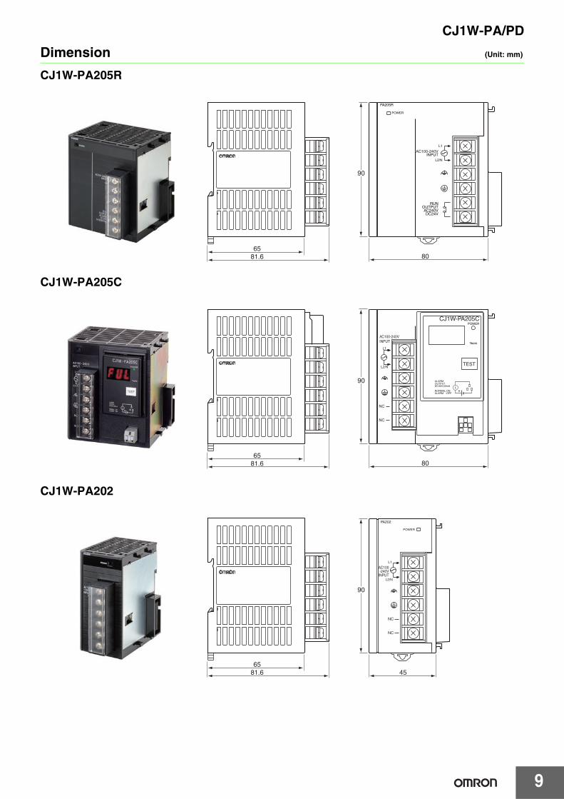
CJ1W-PA/PD
9
Dimension (Unit: mm)
CJ1W-PA205R
CJ1W-PA205C
CJ1W-PA202
POWER
PA205R
DC24VAC240V
OUTPUTRUN
INPUTAC100-240V
L2/N
L1
658081.6
90
Years
POWERCJ1W-PA205C
TEST
NC
NC
AC100-240VINPUT
L2/N
L1
L+
ALARMOUTPUTDC30V,50mA
NORMAL:ONALARM :OFF
658081.6
90
POWER
PA202
INPUT
NC
NC
AC100-240V
L2/N
L1
654581.6
90

10
CJ1W-PA/PD
CJ1W-PD025
CJ1W-PD022
Related Manuals
Cat. No. Name Contents
W393
SYSMAC CJ Series CJ1H-CPU@@H-R, CJ1G/H-CPU@@H, CJ1G-CPU@@P, CJ1G-CPU@@, CJ1M-CPU@@Programmable Controllers Operation Manual
Provides an outlines of and describes the design, installation, maintenance, and other basic operations for the CJ-series PLCs.
POWER
PD025
DC24V+INPUT
NC
NC
656081.6
90
POWER
PD022
652781.6
90

Read and Understand This Catalog Please read and understand this catalog before purchasing the products. Please consult your OMRON representative if you have any questions or comments.
Warranty and Limitations of Liability WARRANTY OMRON's exclusive warranty is that the products are free from defects in materials and workmanship for a period of one year (or other period if specified) from date of sale by OMRON. OMRON MAKES NO WARRANTY OR REPRESENTATION, EXPRESS OR IMPLIED, REGARDING NON-INFRINGEMENT, MERCHANTABILITY, OR FITNESS FOR PARTICULAR PURPOSE OF THE PRODUCTS. ANY BUYER OR USER ACKNOWLEDGES THAT THE BUYER OR USER ALONE HAS DETERMINED THAT THE PRODUCTS WILL SUITABLY MEET THE REQUIREMENTS OF THEIR INTENDED USE. OMRON DISCLAIMS ALL OTHER WARRANTIES, EXPRESS OR IMPLIED. LIMITATIONS OF LIABILITY OMRON SHALL NOT BE RESPONSIBLE FOR SPECIAL, INDIRECT, OR CONSEQUENTIAL DAMAGES, LOSS OF PROFITS OR COMMERCIAL LOSS IN ANY WAY CONNECTED WITH THE PRODUCTS, WHETHER SUCH CLAIM IS BASED ON CONTRACT, WARRANTY, NEGLIGENCE, OR STRICT LIABILITY. In no event shall the responsibility of OMRON for any act exceed the individual price of the product on which liability is asserted. IN NO EVENT SHALL OMRON BE RESPONSIBLE FOR WARRANTY, REPAIR, OR OTHER CLAIMS REGARDING THE PRODUCTS UNLESS OMRON'S ANALYSIS CONFIRMS THAT THE PRODUCTS WERE PROPERLY HANDLED, STORED, INSTALLED, AND MAINTAINED AND NOT SUBJECT TO CONTAMINATION, ABUSE, MISUSE, OR INAPPROPRIATE MODIFICATION OR REPAIR.
Application Considerations SUITABILITY FOR USE OMRON shall not be responsible for conformity with any standards, codes, or regulations that apply to the combination of products in the customer's application or use of the products. At the customer's request, OMRON will provide applicable third party certification documents identifying ratings and limitations of use that apply to the products. This information by itself is not sufficient for a complete determination of the suitability of the products in combination with the end product, machine, system, or other application or use. The following are some examples of applications for which particular attention must be given. This is not intended to be an exhaustive list of all possible uses of the products, nor is it intended to imply that the uses listed may be suitable for the products:
Outdoor use, uses involving potential chemical contamination or electrical interference, or conditions or uses not described in this catalog. Nuclear energy control systems, combustion systems, railroad systems, aviation systems, medical equipment, amusement machines, vehicles,
safety equipment, and installations subject to separate industry or government regulations. Systems, machines, and equipment that could present a risk to life or property.
Please know and observe all prohibitions of use applicable to the products. NEVER USE THE PRODUCTS FOR AN APPLICATION INVOLVING SERIOUS RISK TO LIFE OR PROPERTY WITHOUT ENSURING THAT THE SYSTEM AS A WHOLE HAS BEEN DESIGNED TO ADDRESS THE RISKS, AND THAT THE OMRON PRODUCTS ARE PROPERLY RATED AND INSTALLED FOR THE INTENDED USE WITHIN THE OVERALL EQUIPMENT OR SYSTEM. PROGRAMMABLE PRODUCTS OMRON shall not be responsible for the user's programming of a programmable product, or any consequence thereof.
Disclaimers CHANGE IN SPECIFICATIONS Product specifications and accessories may be changed at any time based on improvements and other reasons. It is our practice to change model numbers when published ratings or features are changed, or when significant construction changes are made. However, some specifications of the products may be changed without any notice. When in doubt, special model numbers may be assigned to fix or establish key specifications for your application on your request. Please consult with your OMRON representative at any time to confirm actual specifications of purchased products. DIMENSIONS AND WEIGHTS Dimensions and weights are nominal and are not to be used for manufacturing purposes, even when tolerances are shown. PERFORMANCE DATA Performance data given in this catalog is provided as a guide for the user in determining suitability and does not constitute a warranty. It may represent the result of OMRON’s test conditions, and the users must correlate it to actual application requirements. Actual performance is subject to the OMRON Warranty and Limitations of Liability. ERRORS AND OMISSIONS The information in this document has been carefully checked and is believed to be accurate; however, no responsibility is assumed for clerical, typographical, or proofreading errors, or omissions.
2012.4
In the interest of product improvement, specifications are subject to change without notice.
OMRON Corporation Industrial Automation Company http://www.ia.omron.com/
(c)Copyright OMRON Corporation 2012 All Right Reserved.

CSM_CJ1W-AD_DA_MAD_DS_E_4_1
1
CJ-Series Analog I/O Unit
CJ1W-AD/DA/MADConsistent Microsecond Throughput:Models with Direct Conversion Join the Lineup
• Analog Input Units for converting analog input signals into binary data
• Analog Output Units for converting binary data into analog output signals
FeaturesAnalog Input Units• Input up to eight analog signals with one Unit.• Functions include line disconnection detection, averaging, peak value holding, offset/gain adjustment, and scaling.
(Offset/gain adjustment is not supported by the CJ1W-AD042. Scaling is supported only by the CJ1W-AD042.)• High-speed A/D conversion in 20 μs/point with direct conversion function * (CJ1W-AD042 only).
Analog Output Units• Output up to eight analog signals with one Unit. • Functions include output holding, offset/gain adjustment, and scaling. (Offset/gain adjustment is not supported by the CJ1W-DA042V. Scaling
is supported only by the CJ1W-DA08V/DA08C/DA042V.)• High-speed D/A conversion in 20 μs/point with direct conversion function * (CJ1W-DA042V only).
Analog I/O Units• Input up to four analog signals and output up to two analog signals with one Unit. • Functions include line disconnection detection, input averaging, scaling, input peak value holding, output holding, ratio conversion, and offset/
gain adjustment.* Direct Conversion Instructions for High-speed type can be used to create a consistent response time from input through data processing and
output. With the Machine Automation Controller NJ-series, the direct conversion function cannot be used. This function is supported only by the CJ-series CPU Unit.
System Configuration
Note: The above diagram is an installation example for the CJ1W-AD081-V1 Analog Input Units and CJ1W-DA041 Analog Output Units.
CJ1W-DA042VCJ1W-AD042
SYSMACCJ1G-CPU44PROGRAMMABLECONTROLLER
RUNERR/ALM
INHPRPHLCOMM
OPEN
PERIHERAL
PORT
MCPWR
BUSY
AD081-V1
B1 A1
MACHNo.x10 1
x10 0
RUNERCERHADJ
MODE
12
DA041
B1 A1
MACHNo.x10 1
x10 0
RUNERCERHADJ
MODE
12
M
M
Analog Output UnitCPU Unit Analog Input Unit
Regulator(Temperature control)
(Position control)
(Speed control)
Servo-controller
Variable speed controller
Preamp
Chart recorder
Transducer
Sensor
SensorTemperature Pressure Speed Flow rate
VoltageCurrentPowerPower factor
M
M

2
CJ1W-AD/DA/MAD
Ordering InformationInternational Standards• The standards are abbreviated as follows: U: UL, U1: UL (Class I Division 2 Products for Hazardous Locations), C: CSA, UC: cULus,
UC1: cULus (Class I Division 2 Products for Hazardous Locations), CU: cUL, N: NK, L: Lloyd, and CE: EC Directives.• Contact your OMRON representative for further details and applicable conditions for these standards.
Analog Input Units
*1 With the Machine Automation Controller NJ-series, the direct conversion function using the AIDC instruction cannot be used.*2 The resolution and conversion speed cannot be set independently. If the resolution is set to 1/4,000, then the conversion speed will be 1 ms/
point.*3 At 23 ±2°C
Analog Output Units
*1 With the Machine Automation Controller NJ-series, the direct conversion function using the AIDC instruction cannot be used.*2 The resolution and conversion speed cannot be set independently. If the resolution is set to 1/4,000, the conversion speed will be 1 ms/point. *3 This is for an external power supply, and not for internal current consumption.
Unit type Product name
I/O points
Signal range
selection
Signal range Resolution Conversion
period
Accuracy at ambient
temperature of 25°C
External connection
No. of unit
numbers allocated
Current consumption
(A) Model Standards
5 V 24 V
CJ1 Special I/O Units
Analog Input Unit
4 inputs
Set separately for each input
1 to 5 V (1/10,000), 0 to 10 V (1/20,000), -5 to 5 V (1/20,000), -10 to 10 V (1/40,000), and 4 to 20 mA (1/10,000)
20 μs/1 point, 25 μs/2 points, 30 μs/3 points, 35 μs/4 pointsThe Direct conversion is provided.*1
Voltage:±0.2% of F.S.Current:±0.4% of F.S.
Removable terminal block
1
0.52 --- CJ1W-AD042 UC1, CE
Analog Input Units
8 inputs 1 to 5 V,
0 to 5 V, 0 to 10 V, -10 to 10 V,4 to 20 mA
1/4,000 (Settable to 1/8,000) *2
1 ms/point (250 μs/point can also be set.)*2
Voltage:±0.2% of F.S.Current:±0.4% of F.S.*3
0.42 ---
CJ1W-AD081-V1
UC1, N, L, CE
4 inputs CJ1W-AD041-V1
Unit type Product name
I/O points
Signal range
selection
Signal range Resolution Conversion
period
Accuracy at ambient
temperature of 25°C
External connection
External power supply
No. of unit
numbers allocated
Current consumption
(A) Model Standards
5 V 24 V
CJ1 Special I/O Units
Analog Output Unit
4 outputs
Set separately for each output
1 to 5 V (1/10,000), 0 to 10 V (1/20,000), and −10 to 10 V (1/40,000)
20 μs/1 point, 25 μs/2 points, 30 μs/3 points, 35 μs/4 pointsThe Direct conver-sion is provided.*1
±0.3% of F.S.
Removable terminal block
---
1
0.40 --- CJ1W-DA042V UC1, CE
Analog Output Units
8 outputs
1 to 5 V, 0 to 5 V, 0 to 10 V, −10 to 10 V
1/4,000 (Settable to 1/8,000)*2
1 ms/point (Settable to 250 μs/point)*2
±0.3% of F.S.
24 VDC
,140 mA max.
0.14
0.14*3 CJ1W-DA08V UC1, N,
L, CE
8 outputs
4 to 20 mA
24 VDC
,170 mA max.
0.17*3 CJ1W-DA08C UC1, N,
CE
4 outputs 1 to 5 V,
0 to 5 V, 0 to 10 V,−10 to 10 V, 4 to 20 mA
1/4,000 1 ms/point
Voltage:±0.3% of F.S.Current:±0.5% of F.S.
24 VDC
,200 mA max.
0.12
0.2*3 CJ1W-DA041
UC1, N, L, CE
2 outputs
24 VDC
,140 mA max.
0.14*3 CJ1W-DA021
High-speed type
High-speed type
+10%−15%
+10%−15%
+10%−15%
+10%−15%

CJ1W-AD/DA/MAD
3
Analog I/O Units
Note: The resolution and conversion speed cannot be set independently. If the resolution is set to 1/4,000, then the conversion speed will be 1 ms/point.
Accessories
Mountable Racks
Note: It may not be possible to mount this many Units to a Rack depending on the current consumption of the other Units.*1 This is the number of Units for a CJ2H-CPU6@ CJ2H CPU Unit (without EtherNet/IP) and a CJ1W-PA205@ or CJ1W-PD025 Power Supply Unit.*2 This is the number of Units for a CJ1W-PA205@ or CJ1W-PD025 Power Supply Unit.*3 A CP1W-EXT01 CJ Unit Adaptor is required.*4 This is the number of Units for a NJ501 CPU Unit, and a NJ-PA3001 or NJ-PD3001 Power Supply Unit.*5 This is the number of Units for a NJ-PA3001 or NJ-PD3001 Power Supply Unit.
Unit type Product name
I/O points
Signal range
selection
Signal range Resolution Conversion
period
Accuracy at ambient
temperature of 25°C
External connection
No. of unit
numbers allocated
Current consumption
(A) Model Standards
5 V 24 V
CJ1 Special I/O Units
Analog I/O Units
4 inputs Set
separately for each input and output
1 to 5 V, 0 to 5 V, 0 to 10 V, −10 to 10 V, 4 to 20 mA
1/4,000 (Settable to 1/8,000)
1 ms/point(Settable to 500 μs/point)
Voltage:±0.2% of F.S.Current:±0.2% of F.S. Removable
terminal block
1 0.58 − CJ1W-MAD42 UC1, N, L, CE
2 outputs
Voltage:±0.3% of F.S.Current:±0.3% of F.S.
Model Accessories
CJ1W-AD081-V1/AD041-V1CJ1W-DA08V/DA08C/DA041/DA021CJ1W-DA042VCJ1W-MAD42
None.
CJ1W-AD042 Four jumpers(For a current input, a jumper is used to connect the current input positive terminal and the voltage input positive terminal.)
ModelNJ system CJ system (CJ1, CJ2) CP1H system NSJ system
CPU Rack Expansion Rack CPU Rack Expansion Backplane CP1H PLC NSJ Controller Expansion
Backplane
CJ1W-AD042 7 Units *410 Units *5
(per Expansion Rack)
8 Units *19 Units *2
(per Expansion Backplane)
2 Units *3 Not supported
9 Units *2(per Expansion
Backplane)
CJ1W-AD081-V19 Units *4
10 Units *5(per Expansion
Rack)
10 Units *110 Units *2
(per Expansion Backplane)
10 Units *2(per Expansion
Backplane)
CJ1W-AD041-V1
CJ1W-DA042V
10 Units *410 Units *5
(per Expansion Rack)
CJ1W-DA08V
CJ1W-DA08C
CJ1W-DA041
CJ1W-DA021
CJ1W-MAD42 7 Units *410 Units *5
(per Expansion Rack)
7 Units *18 Units *2
(per Expansion Backplane)
8 Units *2(per Expansion
Backplane)

4
CJ1W-AD/DA/MAD
Individual Specifications
Analog Input Units CJ1W-AD041-V1/AD081-V1/AD042Specifications
*1 Do not apply a voltage higher than 600 V to the terminal block when performing withstand voltage test on this Unit. Otherwise, internal elements may deteriorate.
*2 Input signal ranges can be set for each input.*3 Voltage input or current input are chosen by using the voltage/current switch at the back of the terminal block.*4 To use a current input, connect the positive current input terminal and positive voltage input terminal with the enclosed short bar. *5 The Analog Input Unit must be operated according to the input specifications provided here. Operating the Unit outside these specifications
will cause the Unit to malfunction. *6 The resolution can be set to 8,000 and the conversion period to 250 μs in the setting. There is only one setting for both of these, i.e., they are
both enabled or disabled together.*7 The accuracy is given for full scale. For example, an accuracy of ±0.2% means a maximum error of ±8 (BCD) at a resolution of 4,000.
For the CJ1W-AD041-V1/ AD081-V1, the default setting is adjusted for voltage input. To use current input, perform the offset and gain adjustments as required.
*8 For the CJ1W-AD041-V1/ AD081-V1, 23±2°C.*9 The A/D conversion period is the time required from when the Analog Input Unit receives the analog signal until it stores the converted value
in internal memory. It takes at least one cycle for the converted data to be stored in the CPU Unit. (The direct conversion function of the CJ1W-AD042 is can be used to input data immediately to the CPU Unit.)
*10 Line disconnection detection is supported only when the range is set to 1 to 5 V or 4 to 20 mA. If there is no input signal when the 1 to 5 V or 4 to 20 mA range is set, the Line Disconnection Flag will turn ON.
Item CJ1W-AD041-V1 CJ1W-AD081-V1 CJ1W-AD042
Unit type CJ-series Special I/O Unit
Isolation *1 Between I/O and Controller signals: Photocoupler (No isolation between I/O signals.)
Between I/O and Controller signals: Digital isolator (No isolation between I/O signals.)
External terminals 18-point detachable terminal block (M3 screws)
Power consumption 420 mA max. at 5 VDC 520 mA max. at 5 VDC
Dimensions (mm) 31 × 90 × 65 mm (W × H × D)
Weight 140 g max. 150 g max.
General specifications Conforms to general specifications for CJ Series.
Input specifications
Number of analog inputs 4 8 4
Input signal range *2
1 to 5 V0 to 5 V0 to 10 V−10 to 10 V4 to 20 mA*3
1 to 5 V0 to 10 V−5 to 5 V−10 to 10 V4 to 20 mA*4
Maximum rated input (for 1 point) *5
Voltage Input: ±15 VCurrent Input: ±30 mA
Input impedance Voltage Input: 1 MΩ min. Current Input: 250 Ω (rated value)
Resolution 4,000/8,000 *6
1 to 5 V 10,000
0 to 10 V 20,000
−5 to 5 V 20,000
−10 to 10 V 40,000
4 to 20 mA 10,000
Converted output data 16-bit binary data
Accuracy *725°C *8 Voltage Input: ±0.2% of F.S.Current Input: ±0.4% of F.S.
0°C to 55°C Voltage Input: ±0.4% of F.S.Current Input: ±0.6% of F.S.
A/D conversion period *9 1 ms/250 μs per point *6 20 μs/1 point, 25 μs/2 points, 30 μs/3 points, 35 μs/4 points
Input functions
Mean value processingStores the last "n" data conversions in the buffer, and stores the mean value of the conversion values.Buffer number: n = 2, 4, 8, 16, 32, 64
Stores the last "n" data conversions in the buffer, and stores the mean value of the conversion values.Buffer number: n = 2, 4, 8, 16, 32, 64, 128, 256, 512
Peak value holding Stores the maximum conversion value while the Peak Value Hold Bit is ON.
Scaling ---
Setting values in any specified unit within a range of ±32,000 as the upper and lower limits allows A/D conversion to be executed and analog signals to be output with these values as full scale.
Input disconnection detection Detects the disconnection and turns ON the Disconnection Detection Flag. *10
Offset/gain adjustment Supported ---
Direct conversion ---
A/D conversion is performed and the converted value is refreshed when the ANALOG INPUT DIRECT CON-VERSION instruction (AIDC) is exe-cuted. This instruction is supported by the CJ2H-CPU@@ (-EIP) CPU Units with unit version 1.1 or later, and CJ2M-CPU@@. CJ1, NJ501, and CP1H CPU Units and NSJ Controllers do not support direct conversion.

CJ1W-AD/DA/MAD
5
Analog Output Units CJ1W-DA021/DA041/DA08V/DA08C/DA042VSpecifications
*1 Do not apply a voltage higher than 600 V to the terminal block when performing withstand voltage test on this Unit.*2 The maximum number of Analog Output Units that can be mounted to one Rack varies depending on the current consumption of the other
Units mounted to the Rack.Select a 24 VDC power supply based on the surge current. The following OMRON external power supplies are recommended.
*3 Output signal ranges can be set for each output.*4 The accuracy is given for full scale. For example, an accuracy of ±0.3% means a maximum error of ±60 mV for a −10 to 10 V range. For the
CJ1W-DA021/041, the accuracy is at the factory setting for a current output. When using a voltage output, adjust the offset gain as required.
Item CJ1W-DA021 CJ1W-DA041 CJ1W-DA08V CJ1W-DA08C CJ1W-DA042V
Unit type CJ-series Special I/O Unit
Isolation *1 Between I/O and Controller signals: Photocoupler (No isolation between I/O signals.)Between I/O and Controller sig-nals: Digital isolator (No isola-tion between I/O signals.)
External terminals 18-point detachable terminal block (M3 screws)
Power consumption 5 VDC, 120 mA max. 5 VDC, 140 mA max. 5 VDC, 400 mA max.
External power supply *224 VDC (inrush current: 20 A max., pulse width: 1 ms min.) ---
140 mA max. 200 mA max. 140 mA max. 170 mA max. ---
Dimensions (mm) 31 × 90 × 65 mm (W × H × D)
Weight 150 g max.
General specifications Conforms to general specifications for CJ-series Series.
Output specifica-tions
Number of analog outputs 2 4 8 8 4
Output signal range *31 to 5 V/4 to 20 mA0 to 5 V0 to 10 V−10 to 10 V
1 to 5 V0 to 5 V0 to 10 V−10 to 10 V
4 to 20 mA1 to 5 V0 to 10 V−10 to 10 V
Output impedance 0.5 Ω max. (for voltage output) 0.5 Ω max. (for voltage output) --- 0.5 Ω max.
(for voltage output)
Max. output current (for 1 point) 12 mA (for voltage output) 2.4 mA
(for voltage output) --- 2 mA (for voltage output)
Maximum permissible load resistance 600 Ω (current output) --- 350 Ω ---
Resolution 4,000 4,000/8,000 *8
1 to 5 V 10,000
0 to 10 V 20,000
-10 to 10 V 40,000
Set data 16-bit binary data
Accuracy *4
25°C Voltage output: ±0.3% of F.S.Current output: ±0.5% of F.S. ±0.3% of F.S. ±0.3% of F.S. ±0.3% of F.S.
0°C to 55°C Voltage output: ±0.5% of F.S.Current output: ±0.8% of F.S. ±0.5% of F.S. ±0.6% of F.S. ±0.5% of F.S.
D/A conversion period *5 1.0 ms per point 1.0 ms or 250 μs per point *8
20 μs/1 point, 25 μs/2 points, 30 μs/3 points, 35 μs/4 points
Output functions
Output hold function
Outputs the specified output status (CLR, HOLD, or MAX) under any of the following circumstances.• When the Conversion Enable Bit is OFF. *6• In adjustment mode, when a value other than the output number is output during adjustment. *7• When output setting value error occurs or Controller operation stops.• When the Load is OFF.
Scaling ---
Supported only for a conversion period of 1 ms and resolution of 4,000.Setting values in any specified unit within a range of ±32,000 as the upper and lower limits allows D/A conversion to be execut-ed and analog signals to be output with these values as full scale.
Setting values in any specified unit within a range of ±32,000 as the upper and lower limits allows D/A conversion to be executed and analog signals to be output with these values as full scale.
Offset/gain adjustment Supported ---
Direct conversion ---
D/A conversion is performed and the output value is re-freshed when the ANALOG OUTPUT DIRECT CONVER-SION instruction (AODC) is ex-ecuted. This instruction is supported by the CJ2H-CPU@@ (-EIP) CPU Units with unit version 1.1 or later, and CJ2M-CPU@@. CJ1, NJ501, and CP1H CPU Units and NSJ Controllers do not support direct conversion.
Manufacturer Model number Specifications
OMRON
S8VS-06024 100 to 240 VAC, 60 W
S8VS-12024 100 to 240 VAC, 120 W
S8VM-05024 100 to 240 VAC, 50 W
S8VM-10024 100 to 240 VAC, 100 W
+10% −15%
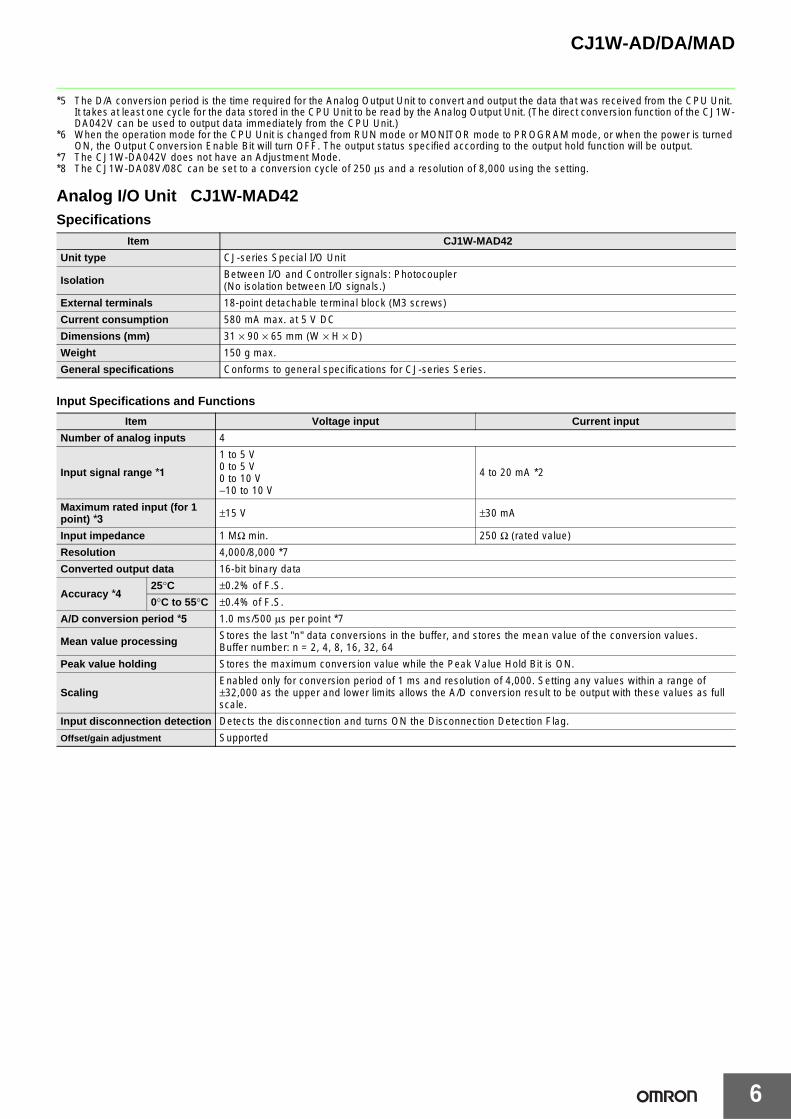
6
CJ1W-AD/DA/MAD
*5 The D/A conversion period is the time required for the Analog Output Unit to convert and output the data that was received from the CPU Unit. It takes at least one cycle for the data stored in the CPU Unit to be read by the Analog Output Unit. (The direct conversion function of the CJ1W-DA042V can be used to output data immediately from the CPU Unit.)
*6 When the operation mode for the CPU Unit is changed from RUN mode or MONITOR mode to PROGRAM mode, or when the power is turned ON, the Output Conversion Enable Bit will turn OFF. The output status specified according to the output hold function will be output.
*7 The CJ1W-DA042V does not have an Adjustment Mode.*8 The CJ1W-DA08V/08C can be set to a conversion cycle of 250 μs and a resolution of 8,000 using the setting.
Analog I/O Unit CJ1W-MAD42Specifications
Input Specifications and Functions
Item CJ1W-MAD42
Unit type CJ-series Special I/O Unit
Isolation Between I/O and Controller signals: Photocoupler(No isolation between I/O signals.)
External terminals 18-point detachable terminal block (M3 screws)
Current consumption 580 mA max. at 5 V DC
Dimensions (mm) 31 × 90 × 65 mm (W × H × D)
Weight 150 g max.
General specifications Conforms to general specifications for CJ-series Series.
Item Voltage input Current input
Number of analog inputs 4
Input signal range *1
1 to 5 V0 to 5 V0 to 10 V−10 to 10 V
4 to 20 mA *2
Maximum rated input (for 1 point) *3 ±15 V ±30 mA
Input impedance 1 MΩ min. 250 Ω (rated value)
Resolution 4,000/8,000 *7
Converted output data 16-bit binary data
Accuracy *425°C ±0.2% of F.S.
0°C to 55°C ±0.4% of F.S.
A/D conversion period *5 1.0 ms/500 μs per point *7
Mean value processing Stores the last "n" data conversions in the buffer, and stores the mean value of the conversion values.Buffer number: n = 2, 4, 8, 16, 32, 64
Peak value holding Stores the maximum conversion value while the Peak Value Hold Bit is ON.
ScalingEnabled only for conversion period of 1 ms and resolution of 4,000. Setting any values within a range of ±32,000 as the upper and lower limits allows the A/D conversion result to be output with these values as full scale.
Input disconnection detection Detects the disconnection and turns ON the Disconnection Detection Flag.
Offset/gain adjustment Supported

CJ1W-AD/DA/MAD
7
Output Specifications
*1 Input and output signal ranges can be set for each input and output.*2 Voltage input or current input are chosen by using the voltage/current switch at the back of the terminal block.*3 The Analog I/O Unit must be operated according to the input specifications provided here. Operating the Unit outside these specifications will
cause the Unit to malfunction.*4 The accuracy is given for full scale. For example, for an input, an accuracy of ±0.2% means a maximum error of ±8 (BCD) at a resolution of
4,000. For an output, an accuracy of ±0.3% means a maximum error of ±60 mV for a −10 to 10 V range.*5 The A/D conversion period is the time required from when the Analog Input Unit receives the analog signal until it stores the converted value
in internal memory. It takes at least one cycle for the converted data to be stored in the CPU Unit. The D/A conversion period is the time required for the Analog Output Unit to convert and output the data that was received from the CPU Unit. It takes at least one cycle for the data stored in the CPU Unit to be read by the Analog Output Unit.
*6 When the operation mode for the CPU Unit is changed from RUN mode or MONITOR mode to PROGRAM mode, or when the power is turned ON, the Output Conversion Enable Bit will turn OFF. The output status specified according to the output hold function will be output.
*7 By means of the setting, the resolution can be changed to 8,000, and the conversion period can be changed to 500 μs.
Item Voltage output Current output
Number of analog outputs 2
Output signal range *1
1 to 5 V0 to 5 V0 to 10 V−10 to 10 V
4 to 20 mA
Output impedance 0.5 Ω max. −Maximum external output current (for 1 point) 2.4 mA −
Maximum allowed load resistance − 600 Ω
Resolution 4,000/8,000 *7
Set data 16-bit binary data
Accuracy *425°C ±0.3% of F.S. ±0.3% of F.S.
0°C to 55°C ±0.5% of F.S. ±0.6% of F.S.
D/A conversion period *5 1.0 ms/500 μs per point
Output hold function
Outputs the specified output status (CLR, HOLD, or MAX) under any of the following circumstances.• When the Conversion Enable Bit is OFF. *6• In adjustment mode, when a value other than the output number is output during adjustment.• When output setting value error occurs or Controller operation stops.• When the Load is OFF.
ScalingEnabled only for conversion period or 1 ms and resolution of 4,000. Setting any values within a range of ±32,000 as the upper and lower limits allows D/A conversion to be executed and analog signals to be output with these values as full scale.
Ratio conversion function *5
Stores the results of positive and negative gradient analog inputs calculated for ratio and bias as analog output values.Positive gradient: Analog output = A × Analog input + B
(A: 0 to 99.99, B: 8000 to 7FFF hex)Negative gradient:Analog output = F − A × Analog input + B
(A: 0 to 99.99, B: 8000 to 7FFF hex, F: Output range maximum value)
Offset/gain adjustment Supported

8
CJ1W-AD/DA/MAD
External Interface
Analog Input Units CJ1W-AD041-V1/AD081-V1/AD042Components
IndicatorsThe indicators show the operating status of the Unit. The following table shows the meanings of the indicators.
* The ADJ LED is not provided with the CJ1W-AD042.
LED Meaning Indicator Operating status
RUN (green) OperatingLit Operating in normal mode.
Not lit Unit has stopped exchanging data with the CPU Unit.
ERC (red) Error detected by UnitLit
Alarm has occurred (such as disconnection detection) or initial settings are incorrect.
Not lit Operating normally.
ERH (red) Error in the CPU UnitLit Error has occurred during data exchange with the CPU Unit.
Not lit Operating normally.
ADJ (yellow) * AdjustingFlashing Operating in offset/gain adjustment mode.
Not lit Other than the above.
MACHNo.
AD081-V1RUNERCERH B1 A1ADJ
x101
x100
09
8765
4 3 2109
8765
4 3 21ON
12
MODE
MACHNo.
AD081-V1RUNERCERH B1 A1ADJ
x101
x100
21
21
21
21
09
8765
4 3 2109
8765
4 3 21
ON
ON
ON
ON
ON1
2
MODE
Front
With Terminal Block RemovedWith Terminal Block
Terminal block
Terminal block lock lever (pull down to release terminal block)
Unit number setting switch
Indicators *1
Terminal block
DIN Track mounting pin
Operating mode switch *2
Voltage/current switch *2
Slider
Slider
Side
Expansion connector
*1 The ADJ LED is not provided with the CJ1W-AD042.*2 These switches are not mounted for the CJ1W-AD042.

CJ1W-AD/DA/MAD
9
Input CircuitsThe following diagrams show the internal circuit of the analog input section.
CJ1W-AD041-V1/AD081-V1 CJ1W-AD042
Terminal ArrangementThe signal names corresponding to the connecting terminals are as shown in the following diagram.
CJ1W-AD041-V1 CJ1W-AD081-V1
CJ1W-AD042
Note: 1. Set the analog input number that you use and input signal range for each analog input, using the memory area or support software. The input signal range can be set separately for each input number.
2. The AG terminals are connected to the 0 V analog circuit in the Unit. Connecting shielded input lines can improve noise resistance.3. Do not connect anything to NC terminals.4. To use a current input with the CJ1W-AD042, connect the positive current input terminal and positive voltage input terminal with the
enclosed short bar.5. Connect a surge suppressor to inductive loads in the system (e.g., magnetic contactors, relays, and solenoids).
1 MΩ
15 kΩ 15 kΩ
15 kΩ 15 kΩ
AG (common to all inputs)
Input (+)
Input (–)
AG(analog 0 V)
Input circuit and conversion circuit
1 MΩ
Voltage/currentinput switch
250 Ω
510 kΩ
510 kΩ
2.2 kΩ
2.2 kΩ
AG (common to all inputs)
Input (–)
AG(analog 0 V)
Input circuit and conversion circuit
250 Ω
Current Input (+)
VoltageInput (+)
Input 2 (+)
Input 2 (−)
Input 4 (+)
Input 4 (−)
AG
N.C.
N.C.
N.C.
N.C.
Input 1 (+)
Input 1 (−)
Input 3 (+)
Input 3 (−)
AG
N.C.
N.C.
N.C.
N.C.
B1
B2
B3
B4
B5
B6
B7
B8
B9
A1
A2
A3
A4
A5
A6
A7
A8
A9
Input 2 (+)
Input 2 (−)
Input 4 (+)
Input 4 (−)
AG
Input 6 (+)
Input 6 (−)
Input 8 (+)
Input 8 (−)
Input 1 (+)
Input 1 (−)
Input 3 (+)
Input 3 (−)
AG
Input 5 (+)
Input 5 (−)
Input 7 (+)
Input 7 (−)
B1
B2
B3
B4
B5
B6
B7
B8
B9
A1
A2
A3
A4
A5
A6
A7
A8
A9
Current Input 2 (+)
Voltage Input 2 (+)
Input 2 (−)
AG
Current Input 4 (+)
Voltage Input 4 (+)
Input 4 (−)
AG
N.C.
Current Input 1 (+)
Voltage Input 1 (+)
Input 1 (−)
AG
Current Input 3 (+)
Voltage Input 3 (+)
Input 3 (−)
AG
N.C.
B1
B2
B3
B4
B5
B6
B7
B8
B9
A1
A2
A3
A4
A5
A6
A7
A8
A9

10
CJ1W-AD/DA/MAD
Analog Output Units CJ1W-DA021/041/08V/08C/DA042VComponents
*1 The ADJ LED is not provided with the CJ1W-DA042V.*2 This switch is not mounted for the CJ1W-DA08V, CJ1W-DA08C and CJ1W-DA042V.
IndicatorsThe indicators show the operating status of the Unit. The following table shows the meanings of the indicators.
* The ADJ LED is not provided with the CJ1W-DA042V.
LED Meaning Indicator Operating status
RUN (green) OperatingLit Operating in normal mode.
Not lit Unit has stopped exchanging data with the CPU Unit.
ERC (red) Error detected by UnitLit Alarm has occurred or initial settings are incorrect.
Not lit Operating normally.
ERH (red) Error in the CPU UnitLit Error has occurred during data exchange with the CPU Unit.
Not lit Operating normally.
ADJ (yellow) * AdjustingFlashing Operating in offset/gain adjustment mode.
Not lit Other than the above.
MACHNo.
DA041RUNERCERH B1 A1ADJ
x101
x100
09
8765
4 32109
8765
4 321ON
12
MODE
Front
With Terminal Block
Terminal block lock lever (pull down to release terminal block)
Unit number switches
Indicators *1
Terminal block
Operating mode switch *2
DIN Track mounting pin
Side
Slider
Slider
Expansion connector

CJ1W-AD/DA/MAD
11
Output CircuitsThe following diagrams show the internal circuit of the analog output section.
CJ1W-DA021/DA041/DA08V/DA08CVoltage Output Circuits Current Output Circuits
CJ1W-DA042VVoltage Output Circuits
Terminal ArrangementThe signal names corresponding to the connecting terminals are as shown in the following diagram.
CJ1W-DA021 CJ1W-DA041
CJ1W-DA08V (Voltage Output)and CJ1W-DA08C (Current Output) CJ1W-DA042V
Note: 1. Set the analog input number that you use and input signal range for each analog input, using the memory area or support software. The input signal range can be set separately for each input number.
2. The N.C. terminals are not connected to internal circuit.3. Use a separate power supply from the one used for Basic I/O Units. Faulty Unit operation may be caused by noise if power is supplied
from the same source. (This does not apply to CJ1W-DA042V.)4. Connect a surge suppressor to inductive loads in the system (e.g., magnetic contactors, relays, and solenoids).
Outputswitch and conversion circuit
AMP Voltage output (+)
Voltage output (–)
AG (common to all outputs)
Voltage output section
AMP
Current output section
Current output (+)
Current output (−)
AMPOutputswitch and conversion circuit
Outputswitch and conversion circuit
AMP Voltage output (+)
Voltage output (–)
AG (common to all outputs)
Voltage output 2 (+)
Output 2 (−)
Current output 2 (+)
N.C.
N.C.
N.C.
N.C.
N.C.
0 V
B1
B2
B3
B4
B5
B6
B7
B8
B9
A1
A2
A3
A4
A5
A6
A7
A8
A9
Voltage output 1 (+)
Output 1 (−)
Current output 1 (+)
N.C.
N.C.
N.C.
N.C.
N.C.
24 V
Voltage output 2 (+)
Output 2 (−)
Current output 2 (+)
Voltage output 4 (+)
Output 4 (−)
Current output 4 (+)
N.C.
N.C.
0 V
B1
B2
B3
B4
B5
B6
B7
B8
B9
A1
A2
A3
A4
A5
A6
A7
A8
A9
Voltage output 1 (+)
Output 1 (−)
Current output 1 (+)
Voltage output 3 (+)
Output 3 (−)
Current output 3 (+)
N.C.
N.C.
24 V
Output 2 (+)
Output 2 (−)
Output 4 (+)
Output 4 (−)
Output 6 (+)
Output 6 (−)
Output 8 (+)
Output 8 (−)
0 V
B1
B2
B3
B4
B5
B6
B7
B8
B9
A1
A2
A3
A4
A5
A6
A7
A8
A9
Output 1 (+)
Output 1 (−)
Output 3 (+)
Output 3 (−)
Output 5 (+)
Output 5 (−)
Output 7 (+)
Output 7 (−)
24 V
Output 2 (+)
Output 2 (−)
N.C.
Output 4 (+)
Output 4 (−)
N.C.
N.C.
N.C.
N.C.
B1
B2
B3
B4
B5
B6
B7
B8
B9
A1
A2
A3
A4
A5
A6
A7
A8
A9
Output 1 (+)
Output 1 (−)
N.C.
Output 3 (+)
Output 3 (−)
N.C.
N.C.
N.C.
N.C.

12
CJ1W-AD/DA/MAD
Analog I/O Unit CJ1W-MAD42Components
IndicatorsThe indicators show the operating status of the Unit. The following table shows the meanings of the indicators.
LED Meaning Indicator Operating status
RUN (green) OperatingLit Operating in normal mode.
Not lit Unit has stopped exchanging data with the CPU Unit.
ERC (red) Error detected by UnitLit Alarm has occurred (such as disconnection detection) or initial
settings are incorrect.
Not lit Operating normally.
ADJ (yellow) AdjustingFlashing Operating in offset/gain adjustment mode.
Not lit Other than the above.
ERH (red) Error in the CPU UnitLit Error has occurred during data exchange with the CPU Unit.
Not lit Operating normally.
MACHNo.
MAD42RUNERCERH B1 A1ADJ
x101
x100
09
8765
4 32109
8765
4 321
MACHNo.
MAD42RUNERCERH B1 A1ADJ
x101
x100
21
21
09
8765
4 32109
8765
4 321
ON
ON
FrontWith Terminal Block With Terminal Block Removed
Indicators
Terminal block
Voltage/current switch
DIN Track mounting pin
Terminal block
Terminal block lock lever (pull down to release terminal bloc
User number setting switch
Slider
Expansion connector
Slider
Side

CJ1W-AD/DA/MAD
13
I/O CircuitThe following diagrams show the internal circuit of the analog I/O section.
Input Circuits
Voltage Output Circuits Current Output Circuits
Terminal ArrangementThe signal names corresponding to the connecting terminals are as shown in the following diagram.
CJ1W-MAD42
Note: 1. Set the analog input number that you use and input signal range for each analog input, using the memory area or support software. The input signal range can be set separately for each input number.
2. The AG terminal (A7, B7) is connected to the 0 V analog circuit in the Unit. Connecting shielded input lines can improve noise resistance.3. The N.C. terminals (A4, B4) are not connected to internal circuit.
Wiring Vasic I/O Units with Terminal BlocksCrimp terminalsUse crimp terminals (M3) having the dimensions shown below.
1 MΩ
15 kΩ 15 kΩ
15 kΩ 15 kΩ
AG (common to all inputs)
Input (+)
Input (–)
AG(analog 0 V)
Input circuit and conversion circuit
1 MΩ
Voltage/currentinput switch
250 Ω
Output switch and conversion circuit
AMP Voltage output (+)
Voltage output (–)
AG (common to all outputs)
AMP
AMPCurrent output (+)
Current output (–)
Output switch and conversion circuit
Voltage output 2 (+)
Output 2 (–)
Current output 2 (+)
N.C.
Input 2 (+)
Input 2 (–)
AG
Input 4 (+)
Input 4 (–)
Voltage output 1 (+)
Output 1 (–)
Current output 1 (+)
N.C.
Input 1 (+)
Input 1 (–)
AG
Input 3 (+)
Input 3 (–)
A1
A2
A3
A4
A5
A6
A7
A8
A9
B1
B2
B3
B4
B5
B6
B7
B8
B9
6.2 mm max. 6.2 mm max.

14
CJ1W-AD/DA/MAD
Dimensions (Unit: mm)
CJ1W-AD041-V1/081-V1/AD042CJ1W-DA021/041/08V/08C/DA042VCJ1W-MAD42
Note: The appearance varies with the model.
Related Manuals
Manual name Cat. No. Manual name Application Description
CJ-series Analog I/OUnits Operation Manualfor NJ-series CPU Unit
W490CJ1W-AD0@@-@@CJ1W-DA0@@@CJ1W-MAD42
Learning about the functions and usage of CJseries Analog Input Units, Analog Output Units, and Analog I/O Units for using them in an NJ-series configuration.
The functions and usage of the CJ-series Analog Input Units, Analog Output Units, and Analog I/O Units for using them in an NJ-series configuration are described.
CS/CJ Series Analog I/OUnits Operation Manual W345
CS1W-AD041-V1/081-V1/161CS1W-DA041/08V/08CCS1W-MAD44CJ1W-AD041-V1/081-V1/042CJ1W-DA021/041/08V/08C/042VCJ1W-MAD42
Learning about the functions and usage of CJseries Analog Input Units, Analog Output Units, and Analog I/O Units.
The functions and usage of the CJ-series Analog Input Units, Analog Output Units, and Analog I/O Units for using them in a CJ-series configuration are described.
MACHNo.
AD081-V1RUNERCERH B1 A1ADJ
x101
x100
09
8765 4 321
09
8765 4 321
ON1
2
MODE
2.7
90
31
2.7
65
89
8.2
6.4
17.5
7.62
74.77
Terminal BlockDimensions

Terms and Conditions Agreement Read and understand this catalog. Please read and understand this catalog before purchasing the products. Please consult your OMRON representative if you have any questions or comments. Warranties. (a) Exclusive Warranty. Omron’s exclusive warranty is that the Products will be free from defects in materials and workmanship for a period of twelve months from the date of sale by Omron (or such other period expressed in writing by Omron). Omron disclaims all other warranties, express or implied. (b) Limitations. OMRON MAKES NO WARRANTY OR REPRESENTATION, EXPRESS OR IMPLIED, ABOUT NON-INFRINGEMENT, MERCHANTABILITY OR FITNESS FOR A PARTICULAR PURPOSE OF THE PRODUCTS. BUYER ACKNOWLEDGES THAT IT ALONE HAS DETERMINED THAT THE PRODUCTS WILL SUITABLY MEET THE REQUIREMENTS OF THEIR INTENDED USE. Omron further disclaims all warranties and responsibility of any type for claims or expenses based on infringement by the Products or otherwise of any intellectual property right. (c) Buyer Remedy. Omron’s sole obligation hereunder shall be, at Omron’s election, to (i) replace (in the form originally shipped with Buyer responsible for labor charges for removal or replacement thereof) the non-complying Product, (ii) repair the non-complying Product, or (iii) repay or credit Buyer an amount equal to the purchase price of the non-complying Product; provided that in no event shall Omron be responsible for warranty, repair, indemnity or any other claims or expenses regarding the Products unless Omron’s analysis confirms that the Products were properly handled, stored, installed and maintained and not subject to contamination, abuse, misuse or inappropriate modification. Return of any Products by Buyer must be approved in writing by Omron before shipment. Omron Companies shall not be liable for the suitability or unsuitability or the results from the use of Products in combination with any electrical or electronic components, circuits, system assemblies or any other materials or substances or environments. Any advice, recommendations or information given orally or in writing, are not to be construed as an amendment or addition to the above warranty. See http://www.omron.com/global/ or contact your Omron representative for published information. Limitation on Liability; Etc. OMRON COMPANIES SHALL NOT BE LIABLE FOR SPECIAL, INDIRECT, INCIDENTAL, OR CONSEQUENTIAL DAMAGES, LOSS OF PROFITS OR PRODUCTION OR COMMERCIAL LOSS IN ANY WAY CONNECTED WITH THE PRODUCTS, WHETHER SUCH CLAIM IS BASED IN CONTRACT, WARRANTY, NEGLIGENCE OR STRICT LIABILITY. Further, in no event shall liability of Omron Companies exceed the individual price of the Product on which liability is asserted. Suitability of Use. Omron Companies shall not be responsible for conformity with any standards, codes or regulations which apply to the combination of the Product in the Buyer’s application or use of the Product. At Buyer’s request, Omron will provide applicable third party certification documents identifying ratings and limitations of use which apply to the Product. This information by itself is not sufficient for a complete determination of the suitability of the Product in combination with the end product, machine, system, or other application or use. Buyer shall be solely responsible for determining appropriateness of the particular Product with respect to Buyer’s application, product or system. Buyer shall take application responsibility in all cases. NEVER USE THE PRODUCT FOR AN APPLICATION INVOLVING SERIOUS RISK TO LIFE OR PROPERTY OR IN LARGE QUANTITIES WITHOUT ENSURING THAT THE SYSTEM AS A WHOLE HAS BEEN DESIGNED TO ADDRESS THE RISKS, AND THAT THE OMRON PRODUCT(S) IS PROPERLY RATED AND INSTALLED FOR THE INTENDED USE WITHIN THE OVERALL EQUIPMENT OR SYSTEM. Programmable Products. Omron Companies shall not be responsible for the user’s programming of a programmable Product, or any consequence thereof. Performance Data. Data presented in Omron Company websites, catalogs and other materials is provided as a guide for the user in determining suitability and does not constitute a warranty. It may represent the result of Omron’s test conditions, and the user must correlate it to actual application requirements. Actual performance is subject to the Omron’s Warranty and Limitations of Liability. Change in Specifications. Product specifications and accessories may be changed at any time based on improvements and other reasons. It is our practice to change part numbers when published ratings or features are changed, or when significant construction changes are made. However, some specifications of the Product may be changed without any notice. When in doubt, special part numbers may be assigned to fix or establish key specifications for your application. Please consult with your Omron’s representative at any time to confirm actual specifications of purchased Product. Errors and Omissions. Information presented by Omron Companies has been checked and is believed to be accurate; however, no responsibility is assumed for clerical, typographical or proofreading errors or omissions.
2013.5
In the interest of product improvement, specifications are subject to change without notice.
OMRON Corporation Industrial Automation Company http://www.ia.omron.com/
(c)Copyright OMRON Corporation 2013 All Right Reserved.

CSM_CJ1W-INPUT_DS_E_8_1
1
CJ-series Input Units
CJ1W-ID/IAA Wide Range of Basic Input Units for High Speed Input and Different Applications
• Receive ON/OFF signals from external devices into the PLC System to update I/O memory in the CPU Unit.
• New high-speed input models CJ1W-ID212 and CJ1W-ID233 are now available. These units can help to increase system throughput.
Features• High-speed input models are available, meeting versatile applications.
ON Response Time: 15μs, OFF Response Time: 90μs• Use 24-VDC, 100-VAC, and 200-VAC models to connect to devices with different types of outputs.• The 24-VDC models can be connected to devices with either NPN or PNP outputs. There is no need to select the polarity. *1• A digital filter in the Unit can be set from 0 to 32 ms to reduce the influence of external noise. • Either a Fujitsu or MIL connector interface can be used. *2• Several models of Terminal Block Conversion Units are available, making it easy to connect to external devices.
*1. The same polarity is used for the same common.*2. For models with 32 or 64 inputs.
CJ1W-ID212 CJ1W-ID233

CJ1W-ID/IA
2
Ordering InformationInternational Standards• The standards are abbreviated as follows: U: UL, U1: UL (Class I Division 2 Products for Hazardous Locations), C: CSA, UC: cULus,
UC1: cULus (Class I Division 2 Products for Hazardous Locations), CU: cUL, N: NK, L: Lloyd, and CE: EC Directives.• Contact your OMRON representative for further details and applicable conditions for these standards.
Input Units
AccessoriesConnectors are not included for models with connectors. Either use one of the applicable connector listed below or use an applicable Connector-Terminal Block Conversion Unit or I/O Relay Terminal. For details on wiring methods, refer to External Interface.
Unit type Product name
SpecificationsCurrent
consumption (A)
Model Standards
I/O points Input voltage and current Commons External
connection
No. of words
allocated5 V 24 V
CJ1 Basic I/O Units
DC Input Units
8 inputs 12 to 24 VDC, 10 mAIndependent contacts
Removable terminal block 1 word 0.09 − CJ1W-ID201
UC1, N, L, CE
16 inputs 24 VDC, 7 mA16 points, 1 common
Removable terminal block 1 word 0.08 − CJ1W-ID211
16 inputs(High speed) 24 VDC, 7 mA
16 points,1 common
Removable terminal block 1 word 0.13 − CJ1W-ID212 N, L, CE
32 inputs 24 VDC, 4.1 mA 16 points, 1 common Fujitsu connector 2 words 0.09 − CJ1W-ID231
UC1, N, L, CE
32 inputs 24 VDC, 4.1 mA 16 points, 1 common MIL connector 2 words 0.09 − CJ1W-ID232
32 inputs(High speed) 24 VDC, 4.1 mA 16 points,
1 common MIL connector 2 words 0.20 − CJ1W-ID233 N, L, CE
64 inputs 24 VDC, 4.1 mA 16 points, 1 common Fujitsu connector 4 words 0.09 − CJ1W-ID261
UC1, N, L, CE
64 inputs 24 VDC, 4.1 mA 16 points,1 common MIL connector 4 words 0.09 − CJ1W-ID262
AC Input Units 8 inputs 200 to 24 VAC, 10 mA
(200 V, 50 Hz)8 points, 1 common
Removable Terminal Block 1 words 0.08 − CJ1W-IA201
16 inputs 100 to 120 VAC, 7 mA (100 V, 50 Hz)
16 points, 1 common
Removable Terminal Block 1 words 0.09 − CJ1W-IA111

3
CJ1W-ID/IA
Applicable ConnectorsFujitsu Connectors for 32-input, 32-output, 64-input, 64-output, 32-input/32-output, and 16-input/16-output Units
MIL Connectors for 32-input, 32-output, 64-input, 64-output, 32-input/32-output, and 16-input/16-output Units
* Crimp Contacts are also required. Refer to page 20 for details.
Applicable Connector-Terminal Block Conversion Units
Note: For the combination of Input Units with Connector-Terminal Block Conversion Units, refer to 2. Connecting Connector-Terminal Block Conversion Units.
Name Connection Remarks Applicable Units Model Standards
40-pin Connectors
SolderedFCN-361J040-AU ConnectorFCN-360C040-J2 Connector
CoverFujitsu Connectors: CJ1W-ID231(32 inputs): 1 per UnitCJ1W-ID261 (64 inputs): 2 per UnitCJ1W-OD231 (32 outputs):1 per UnitCJ1W-OD261 (64 outputs): 2 per UnitCJ1W-MD261 (32 inputs, 32 outputs): 2 per Unit
C500-CE404
−
Crimped
FCN-363J040 HousingFCN-363J-AU ContactorFCN-360C040-J2 Connector
Cover
C500-CE405
Pressure welded FCN-367J040-AU/F C500-CE403
24-pin Connectors
SolderedFCN-361J024-AU ConnectorFCN-360C024-J2 Connector
Cover
Fujitsu Connectors:CJ1W-MD231 (16 inputs, 16 outputs): 2 per Unit
C500-CE241
Crimped
FCN-363J024 HousingFCN-363J-AU ContactorFCN-360C024-J2 Connector
Cover
C500-CE242
Pressure welded FCN-367J024-AU/F C500-CE243
Name Connection Remarks Applicable Units Model Standards
40-pin Connectors
Pressure welded FRC5-AO40-3TOSMIL Connectors:CJ1W-ID232/233 (32 inputs): 1 per UnitCJ1W-OD232/233/234 (32 outputs):1 per UnitCJ1W-ID262 (64 inputs): 2 per UnitCJ1W-OD262/263 (64 outputs): 2 per UnitCJ1W-MD263/563 (32 inputs, 32 outputs): 2 per Unit
XG4M-4030-T
−
Crimped − XG5N-401*
20-pin Connectors
Pressure welded FRC5-AO20-3TOS MIL Connectors:CJ1W-MD232/233 (16 inputs, 16 outputs): 2 per Unit
XG4M-2030-T−
Crimped − XG5N-201*
Type Series I/O Number of poles Wiring method Terminal
type
Size MountingCommon terminals
Bleeder resistance Indicators I/O Units Model StandardsDepth
(mm)Height (mm)
Width (mm)
DIN Track Screws
PLCs XW2R Output 34
Phillips screw
M3 50 48.35 130.7
Yes Yes No No No
CJ1W-ID231CJ1W-ID261 XW2R-J34G-C1
−
CJ1W-ID232CJ1W-ID233CJ1W-ID262
XW2R-J34G-C2
Slotted screw (rise up)
M3(Europeantype)
50 45.11 98.5
CJ1W-ID231CJ1W-ID261 XW2R-E34G-C1
CJ1W-ID232CJ1W-ID233CJ1W-ID262
XW2R-E34G-C2
Push-in spring
Clamp 50 45.11 98.5
CJ1W-ID231CJ1W-ID261 XW2R-P34G-C1
CJ1W-ID232CJ1W-ID233CJ1W-ID262
XW2R-P34G-C2

CJ1W-ID/IA
4
Applicable I/O Relay Terminals
Note: For the combination of Input Units with I/O Relay Terminal and Connecting Cables, refer to 3. Connecting I/O Relay Terminals.
Type Series
Specifications Size (horizontal mounting) Mounting
Model StandardsClassification Polarity
Number of
points
Rated ON current at contacts
Operation indicators
Terminal block for
power supply wiring
Horizontal (mm)
Vertical (mm)
Height (mm)
DIN Track Screws
Space-saving G70D
Vertical typeG70D-V
Outputs
Relay outputs
NPN16 (SPST-NO × 16)
5A or 3A
Yes Expandable 135 46 81 Yes Yes
G70D-VSOC16U, C, CEMOSFET
relay outputs
0.3A G70D-VFOM16
Flat typeG70D
Relay outputs
NPN
8 (SPST-NO × 8) 5A
Yes −
68 93 44
Yes Yes
G70D-SOC08 −
16 (SPST-NO × 16)
3A
156 51 39
G70D-SOC16
−
PNP16 (SPST-NO × 16)
3A G70D-SOC16-1
MOSFET relay outputs
NPN 16 (SPST-NO × 16)
0.3AG70D-FOM16
−PNP G70D-FOM16-1
High-capacity, space-saving
G70R Outputs Relay outputs NPN 8 (SPST-
NO × 8) 10A Yes − 136 93 55 Yes Yes G70R-SOC08 −
Standard G7TC
Inputs
AC inputs
NPN16 (SPST-NO × 16)
1A
Yes −
182
85 68 Yes −
G7TC-IA16
U, C
DC inputs G7TC-ID16
Outputs Relay outputs
NPN
8 (SPST-NO × 8)
5A
102 G7TC-OC08
16 (SPST-NO × 16)
182
G7TC-OC16
PNP16 (SPST-NO × 16)
G7TC-OC16-1 −
High-capacity socket
G70A (Socket only)
Outputs Relay outputs
NPN 16 (SPDT × 16 possible with G2R Relays)
10 A (Terminal block allowable current)
No − 234 75 64 Yes −
G70A-ZOC16-3
U, C, CE
(Socket only) + Relay/SSR/MOSFET Relay/Timer
PNP
G70A-ZOC16-4(Socket only) + Relay/SSR/MOSFET Relay/Timer

5
CJ1W-ID/IA
Mountable Racks
ModelNJ system CJ system (CJ1, CJ2) CP1H system NSJ system
CPU Rack Expansion Rack CPU Rack Expansion Backplane CP1H PLC NSJ Controller Expansion
Backplane
CJ1W-ID201
10 Units10 Units
(per Expansion Rack)
10 Units10 Units
(per Expansion Backplane)
Not supported Not supported10 Units
(per Expansion Backplane)
CJ1W-ID211
CJ1W-ID212
CJ1W-ID231
CJ1W-ID232
CJ1W-ID233
CJ1W-ID261
CJ1W-ID262
CJ1W-IA201
CJ1W-IA111

CJ1W-ID/IA
6
SpecificationsCJ1W-ID201 DC Input Unit (12 to 24-VDC, 8 Points)
*1. The ON response time will be 20 μs maximum and OFF response time will be 400 μs maximum even if the response time are set to 0 ms due to internal element delays.
*2. Terminal numbers A0 to A8 and B0 to B8 are used in the external connection and terminal-device variable diagrams. They are not printed on the Units.
Note: Although 16 I/O bits (1 word) are allocated, only 8 of these can be used for external I/O.
Name 8-point DC Input Unit with Terminal Block
Model CJ1W-ID201
Rated Input Voltage 12 to 24 VDC
Rated Input Voltage Range 10.2 to 26.4 VDC
Input Impedance 2.4 kΩ
Input Current 10 mA typical (at 24 VDC)
ON Voltage/ON Current 8.8 VDC min./3 mA min.
OFF Voltage/OFF Current 3 VDC max./1 mA max.
ON Response Time 8.0 ms max. (Can be set to between 0 and 32 ms in the Setup.) *1
OFF Response Time 8.0 ms max. (Can be set to between 0 and 32 ms in the Setup.) *1
Number of Circuits 8 independent circuits
Number of Simultaneously ON Points
100% simultaneously ON
Insulation Resistance 20 MΩ between external terminals and the GR terminal (100 VDC)
Dielectric Strength 1,000 VAC between the external terminals and the GR terminal for 1 minute at a leakage current of 10 mA max.
Internal Current Consumption 80 mA max.
Weight 110 g max.
Circuit Configuration
• The signal names of the terminals are the device variable names. The device variable names are the names that use "Jxx" as the device name.
External connection and terminal-device variable diagram
• Polarity of the input power supply can be connected in either direction.• The signal names of the terminals are the device variable names.
The device variable names are the names that use "Jxx" as the device name.
560
Ω
2.4 kΩ
560
Ω
2.4 kΩ10
00 p
F
Input indicator
Inte
rnal
circ
uits
to
1000
pF
Input indicator
Inte
rnal
circ
uits
Signal name
COM7
Jxx_Ch1_In07
COM0
Jxx_Ch1_In00
Signal name
Signal name
Con-nector pin *2
B1
IN0
B2
IN1
B3
IN2
B4
IN3
B5
IN4
B6
IN5
B7
IN6
B8
IN7
NC
C0
C1
C2
C3
C4
C5
C6
C7
NC
B0A1
A2
A3
A4
A5
A6
A7
A8
A0
12~24V DC

7
CJ1W-ID/IA
CJ1W-ID211 DC Input Unit (24 VDC, 16 Points)
*1. The ON response time will be 20 μs maximum and OFF response time will be 400 μs maximum even if the response time are set to 0 ms due to internal element delays.
*2. Terminal numbers A0 to A8 and B0 to B8 are used in the external connection and terminal-device variable diagrams. They are not printed on the Units.
Name 16-point DC Input Unit with Terminal Block
Model CJ1W-ID211
Rated Input Voltage 24 VDC
Rated Input Voltage Range 20.4 to 26.4 VDC
Input Impedance 3.3 kΩ
Input Current 7 mA typical (at 24 VDC)
ON Voltage/ON Current 14.4 VDC min./3 mA min.
OFF Voltage/OFF Current 5 VDC max./1 mA max.
ON Response Time 8.0 ms max. (Can be set to between 0 and 32 ms in the Setup.) *1
OFF Response Time 8.0 ms max. (Can be set to between 0 and 32 ms in the Setup.) *1
Number of Circuits 16 (16 points/common, 1 circuit)
Number of Simultaneously ON Points
100% simultaneously ON (at 24 VDC) (Refer to the following illustration.)
Insulation Resistance 20 MΩ between external terminals and the GR terminal (100 VDC)
Dielectric Strength 1,000 VAC between the external terminals and the GR terminal for 1 minute at a leakage current of 10 mA max.
Internal Current Consumption 80 mA max.
Weight 110 g max.
Circuit Configuration
• The signal names of the terminals are the device variable names. The device variable names are the names that use "Jxx" as the device name.
External connection and terminal-device variable diagram
• Polarity of the input power supply can be connected in either direction.• The signal names of the terminals are the device variable names.
The device variable names are the names that use "Jxx" as the device name.
Inte
rnal
circ
uits
Input indicator
to
Signal name
1000 pF
470 Ω3.3 kΩJxx_Ch1_In00
Jxx_Ch1_In15
COM
COM
18
16
14
12
10
8
6
4
2
00 10 20 30 40 50 60
No.
of s
imul
tane
ousl
y O
N p
oint
s
Input voltage: 26.4 VDC12 points at 55°C.
16 points at 45°C.
Ambient temperature(°C)
Temperature characteristics for simultaneously ON points
24 VDC
B1
Jxx_Ch1_In01
B2
Jxx_Ch1_In03
B3
Jxx_Ch1_In05
B4
Jxx_Ch1_In07
B5
Jxx_Ch1_In09
B6
Jxx_Ch1_In11
B7
Jxx_Ch1_In13
B8
Jxx_Ch1_In15
COM
A1
Jxx_Ch1_In00
A2
Jxx_Ch1_In02
A3
Jxx_Ch1_In04
A4
Jxx_Ch1_In06
A5
Jxx_Ch1_In08
A6
Jxx_Ch1_In10
A7
Jxx_Ch1_In12
A8
Jxx_Ch1_In14
COM
B0A0
Signal name
Signal name
Connector pin *2

CJ1W-ID/IA
8
CJ1W-ID212 DC Input Unit (24 VDC, 16 Points)
*1. The ON response time will be 15 μs maximum and OFF response time will be 90 μs maximum even if the response time are set to 0 ms due to internal element delays.
*2. Terminal numbers A0 to A8 and B0 to B8 are used in the external connection and terminal-device variable diagrams. They are not printed on the Units.
Name 16-point DC Input Unit with Terminal Block
Model CJ1W-ID212
Rated Input Voltage 24 VDC
Rated Input Voltage Range 20.4 to 26.4 VDC
Input Impedance 3.3 kΩ
Input Current 7 mA typical (at 24 VDC)
ON Voltage/ON Current 14.4 VDC min./3 mA min.
OFF Voltage/OFF Current 5 VDC max./1 mA max.
ON Response Time 8.0 ms max. (Can be set to between 0 and 32 ms in the Setup.) *1
OFF Response Time 8.0 ms max. (Can be set to between 0 and 32 ms in the Setup.) *1
Number of Circuits 16 (16 points/common, 1 circuit)
Number of Simultaneously ON Points
100% simultaneously ON (at 24 VDC) (Refer to the following illustration.)
Insulation Resistance 20 MΩ between external terminals and the GR terminal (100 VDC)
Dielectric Strength 1,000 VAC between the external terminals and the GR terminal for 1 minute at a leakage current of 10 mA max.
Internal Current Consumption 130 mA max.
Weight 110 g max.
Circuit Configuration
• The signal names of the terminals are the device variable names. The device variable names are the names that use "Jxx" as the device name.
External connection and terminal-device variable diagram
• Polarity of the input power supply can be connected in either direction.• The signal names of the terminals are the device variable names.
The device variable names are the names that use "Jxx" as the device name.
1000 pF
470 Ω3.3 kΩ
Inte
rnal
circ
uits
Input indicator
to
Signal name
Jxx_Ch1_In00
Jxx_Ch1_In15
COM
COM
18
16
14
12
10
8
6
4
2
00 10 20 30 40 50 60
No.
of s
imul
tane
ousl
y O
N p
oint
s
Input voltage: 26.4 VDC12 points at 55°C.
16 points at 45°C.
Ambient temperature(°C)
Temperature characteristics for simultaneously ON points
B1
Jxx_Ch1_In01
B2
Jxx_Ch1_In03
B3
Jxx_Ch1_In05
B4
Jxx_Ch1_In07
B5
Jxx_Ch1_In09
B6
Jxx_Ch1_In11
B7
Jxx_Ch1_In13
B8
Jxx_Ch1_In15
COM
A1
Jxx_Ch1_In00
A2
Jxx_Ch1_In02
A3
Jxx_Ch1_In04
A4
Jxx_Ch1_In06
A5
Jxx_Ch1_In08
A6
Jxx_Ch1_In10
A7
Jxx_Ch1_In12
A8
Jxx_Ch1_In14
COM
B0A0
24 VDC
Signal name
Signal name
Connector pin *2

9
CJ1W-ID/IA
CJ1W-ID231 DC Input Unit (24 VDC, 32 Points)
* The ON response time will be 20 μs maximum and OFF response time will be 400 μs maximum even if the response times are set to 0 ms due to internal element delays.
Note: Observe the following restrictions when connecting to a 2-wire sensor. • Make sure the input power supply voltage is larger than the ON voltage (19 V) plus the residual voltage of the sensor (approx. 3 V). • Use a sensor with a minimum load current of 3 mA min. • Connect bleeder resistance if you connect a sensor with a minimum load current of 5 mA or higher.
Name 32-point DC Input Unit with Fujitsu Connector
Model CJ1W-ID231
Rated Input Voltage 24 VDC
Rated Input Voltage Range 20.4 to 26.4 VDC
Input Impedance 5.6 kΩ
Input Current 4.1 mA typical (at 24 VDC)
ON Voltage/ON Current 19.0 VDC min./3 mA min.
OFF Voltage/OFF Current 5 VDC max./1 mA max.
ON Response Time 8.0 ms max. (Can be set to between 0 and 32 in the Setup.) *
OFF Response Time 8.0 ms max. (Can be set to between 0 and 32 in the Setup.) *
Number of Circuits 32 (16 points/common, 2 circuits)
Number of Simultaneously ON Points 75% (12 points/common) simultaneously ON (at 24 VDC) (Refer to the following illustration.)
Insulation Resistance 20 MΩ between external terminals and the GR terminal (100 VDC)
Dielectric Strength 1,000 VAC between the external terminals and the GR terminal for 1 minute at a leakage current of 10 mA max.
Internal Current Consumption 90 mA max.
Weight 70 g max.
Accessories None
Circuit Configuration
• The signal names of the terminals are the device variable names. The device variable names are the names that use "Jxx" as the device name.
External connection and terminal-device variable diagram
• The input power polarity can be connected in either direction.• Be sure to wire both pins A9 and A18 (COM0), and set the same polarity for both pins.• Be sure to wire both pins B9 and B18 (COM1), and set the same polarity for both pins.• The signal names of the terminals are the device variable names.
The device variable names are the names that use "Jxx" as the device name.
560
Ω56
0 Ω
5.6 kΩ
5.6 kΩ
1000
pF
1000
pF
Inte
rnal
circ
uits
Input indicator
to
toWd m+1
Wd m
Allocated CIO word
Signal name
Connector row A
Connector row B
Jxx_Ch1_In00
Jxx_Ch1_In15
COM0
Jxx_Ch2_In00
Jxx_Ch2_In15
COM1
COM0
COM1
SW
0
5
10
15
20
25
30
35
0 10 20 30 40 50 60
Number of Simultaneously ON Points vs. Ambient Temperature Characteristic
Num
ber
of s
imul
tane
ousl
y O
N p
oint
s
Ambient Temperature
(°C)
10 points/common at 55°C
12 points/common at 55°C
Input voltage: 26.4 VDC
Input voltage: 24 VDC
32 points at 48°C32 points at 40°C
AllocatedCIO word
AllocatedCIO word
Wd m+1Wd m 24 VDC
Wd m Wd m+1
24 VDC
Signal name
Signal name
Connec-tor pin
Jxx_Ch1_In00
Jxx_Ch1_In01
Jxx_Ch1_In02
Jxx_Ch1_In03
Jxx_Ch1_In04
Jxx_Ch1_In05
Jxx_Ch1_In06
Jxx_Ch1_In07
Jxx_Ch2_In00
Jxx_Ch2_In01
Jxx_Ch2_In02
Jxx_Ch2_In03
Jxx_Ch2_In04
Jxx_Ch2_In05
Jxx_Ch2_In06
Jxx_Ch2_In07
COM0
Jxx_Ch1_In08
Jxx_Ch1_In09
Jxx_Ch1_In10
Jxx_Ch1_In11
Jxx_Ch1_In12
Jxx_Ch1_In13
Jxx_Ch1_In14
Jxx_Ch1_In15
Jxx_Ch2_In08
Jxx_Ch2_In09
Jxx_Ch2_In10
Jxx_Ch2_In11
Jxx_Ch2_In12
Jxx_Ch2_In13
Jxx_Ch2_In14
Jxx_Ch2_In15
COM0
NC
NC
COM1
COM1
NC
NC
A1
A2
A3
A4
A5
A6
A7
A8
A9
A10
A11
A12
A13
A14
A15
A16
A17
A18
A19
A20
B1
B2
B3
B4
B5
B6
B7
B8
B9
B10
B11
B12
B13
B14
B15
B16
B17
B18
B19
B20

CJ1W-ID/IA
10
CJ1W-ID232 DC Input Unit (24 VDC, 32 Points)
* The ON response time will be 20 μs maximum and OFF response time will be 400 μs maximum even if the response times are set to 0 ms due to internal element delays.
Note: Observe the following restrictions when connecting to a 2-wire sensor. • Make sure the input power supply voltage is larger than the ON voltage (19 V) plus the residual voltage of the sensor (approx. 3 V). • Use a sensor with a minimum load current of 3 mA min. • Connect bleeder resistance if you connect a sensor with a minimum load current of 5 mA or higher.
Name 32-point DC Input Unit with MIL Connector
Model CJ1W-ID232
Rated Input Voltage 24 VDC
Rated Input Voltage Range 20.4 to 26.4 VDC
Input Impedance 5.6 kΩInput Current 4.1 mA typical (at 24 VDC)
ON Voltage/ON Current 19.0 VDC min./3 mA min.
OFF Voltage/OFF Current 5 VDC max./1 mA max.
ON Response Time 8.0 ms max. (Can be set to between 0 and 32 in the Setup.) *
OFF Response Time 8.0 ms max. (Can be set to between 0 and 32 in the Setup.) *
Number of Circuits 32 (16 points/common, 2 circuits)
Number of Simultaneously ON Points 75% (12 points/common) simultaneously ON (at 24 VDC) (Refer to the following illustration.)
Insulation Resistance 20 MΩ between external terminals and the GR terminal (100 VDC)
Dielectric Strength 1,000 VAC between the external terminals and the GR terminal for 1 minute at a leakage current of 10 mA max.
Internal Current Consumption 90 mA max.
Weight 70 g max.
Accessories None
Circuit Configuration
• The signal names of the terminals are the device variable names. The device variable names are the names that use "Jxx" as the device name.
External connection and terminal-device variable diagram
• The input power polarity can be connected in either direction.• Be sure to wire both pins 23 and 24 (COM0), and set the same polarity for both pins.• Be sure to wire both pins 3 and 4 (COM1), and set the same polarity for both pins.• The signal names of the terminals are the device variable names.
The device variable names are the names that use "Jxx" as the device name.
560
Ω56
0 Ω
5.6 kΩ
5.6 kΩ
1000
pF
1000
pF
Inte
rnal
circ
uits
Input indicator
to
toWd m+1
Wd m
Allocated CIO word
Signal name
Connector row A
Connector row B
Jxx_Ch1_In00
Jxx_Ch1_In15
COM0
Jxx_Ch2_In00
Jxx_Ch2_In15
COM1
COM0
COM1
SW
0
5
10
15
20
25
30
35
0 10 20 30 40 50 60Num
ber
of s
imul
tane
ousl
y O
N p
oint
s
Ambient Temperature(°C)
10 points/common at 55°C
12 points/common at 55°C
Input voltage: 26.4 VDC
Input voltage: 24 VDC
32 points at 48°C32 points at 40°C
Number of Simultaneously ON Points vs. Ambient Temperature Characteristic
Wd m+1 Wd m+1
Wd m Wd m
24 VDC
24 VDC
Signal name
Signal name
Connec-tor pin
Allocated CIO word
Allocated CIO word
2 NC
4 COM1
6 Jxx_Ch2_In07
8 Jxx_Ch2_In06
10 Jxx_Ch2_In05
12 Jxx_Ch2_In04
14 Jxx_Ch2_In03
16 Jxx_Ch2_In02
18 Jxx_Ch2_In01
20 Jxx_Ch2_In00
Jxx_Ch1_In07
Jxx_Ch1_In06
Jxx_Ch1_In05
Jxx_Ch1_In04
Jxx_Ch1_In03
Jxx_Ch1_In02
Jxx_Ch1_In01
Jxx_Ch1_In00
22 NC
24262830323436
1NC
3COM1
5Jxx_Ch2_In15
7Jxx_Ch2_In14
9Jxx_Ch2_In13
11Jxx_Ch2_In12
13Jxx_Ch2_In11
15Jxx_Ch2_In10
17Jxx_Ch2_In09
19Jxx_Ch2_In08
21NC
23252729313335
3840
3739
COM0 COM0
Jxx_Ch1_In15
Jxx_Ch1_In14
Jxx_Ch1_In13
Jxx_Ch1_In12
Jxx_Ch1_In11
Jxx_Ch1_In10
Jxx_Ch1_In09
Jxx_Ch1_In08

11
CJ1W-ID/IA
CJ1W-ID233 DC Input Unit (24 VDC, 32 Points)
* The ON response time will be 15 μs maximum and OFF response time will be 90 μs maximum even if the response times are set to 0 ms due to internal element delays.
Note: Observe the following restrictions when connecting to a 2-wire sensor. • Make sure the input power supply voltage is larger than the ON voltage (19 V) plus the residual voltage of the sensor (approx. 3 V). • Use a sensor with a minimum load current of 3 mA min. • Connect bleeder resistance if you connect a sensor with a minimum load current of 5 mA or higher.
Name 32-point DC Input Unit with MIL Connector
Model CJ1W-ID233
Rated Input Voltage 24 VDC
Rated Input Voltage Range 20.4 to 26.4 VDC
Input Impedance 5.6 kΩInput Current 4.1 mA typical (at 24 VDC)
ON Voltage/ON Current 19.0 VDC min./3 mA min.
OFF Voltage/OFF Current 5 VDC max./1 mA max.
ON Response Time 8.0 ms max. (Can be set to between 0 and 32 in the Setup.) *
OFF Response Time 8.0 ms max. (Can be set to between 0 and 32 in the Setup.) *
Number of Circuits 32 (16 points/common, 2 circuits)
Number of Simultaneously ON Points 75% (12 points/common) simultaneously ON (at 24 VDC) (Refer to the following illustration.)
Insulation Resistance 20 MΩ between external terminals and the GR terminal (100 VDC)
Dielectric Strength 1,000 VAC between the external terminals and the GR terminal for 1 minute at a leakage current of 10 mA max.
Internal Current Consumption 200 mA max.
Weight 70 g max.
Accessories None
Circuit Configuration
• The signal names of the terminals are the device variable names. The device variable names are the names that use "Jxx" as the device name.
External connection and terminal-device variable diagram
• The input power polarity can be connected in either direction.• Be sure to wire both pins 23 and 24 (COM0), and set the same polarity for both pins.• Be sure to wire both pins 3 and 4 (COM1), and set the same polarity for both pins.• The signal names of the terminals are the device variable names.
The device variable names are the names that use "Jxx" as the device name.
560
Ω56
0 Ω
5.6 kΩ
5.6 kΩ
1000
pF
1000
pF
Inte
rnal
circ
uits
Input indicator
to
toWd m+1
Wd m
Allocated CIO word
Signal name
Connector row A
Connector row B
Jxx_Ch1_In00
Jxx_Ch1_In15
COM0
Jxx_Ch2_In00
Jxx_Ch2_In15
COM1
COM0
COM1
SW
0
5
10
15
20
25
30
35
0 10 20 30 40 50 60Num
ber
of s
imul
tane
ousl
y O
N p
oint
s
Ambient Temperature(°C)
10 points/common at 55°C
12 points/common at 55°C
Input voltage: 26.4 VDC
Input voltage: 24 VDC
32 points at 48°C32 points at 40°C
Number of Simultaneously ON Points vs. Ambient Temperature Characteristic
Wd m+1 Wd m+1
Wd m Wd m
24 VDC
24 VDC
Signal name
Signal name
Connec-tor pin
Allocated CIO word
Allocated CIO word
2 NC
4 COM1
6 Jxx_Ch2_In07
8 Jxx_Ch2_In06
10 Jxx_Ch2_In05
12 Jxx_Ch2_In04
14 Jxx_Ch2_In03
16 Jxx_Ch2_In02
18 Jxx_Ch2_In01
20 Jxx_Ch2_In00
Jxx_Ch1_In07
Jxx_Ch1_In06
Jxx_Ch1_In05
Jxx_Ch1_In04
Jxx_Ch1_In03
Jxx_Ch1_In02
Jxx_Ch1_In01
Jxx_Ch1_In00
22 NC
24262830323436
1NC
3COM1
5Jxx_Ch2_In15
7Jxx_Ch2_In14
9Jxx_Ch2_In13
11Jxx_Ch2_In12
13Jxx_Ch2_In11
15Jxx_Ch2_In10
17Jxx_Ch2_In09
19Jxx_Ch2_In08
21NC
23252729313335
3840
3739
COM0 COM0
Jxx_Ch1_In15
Jxx_Ch1_In14
Jxx_Ch1_In13
Jxx_Ch1_In12
Jxx_Ch1_In11
Jxx_Ch1_In10
Jxx_Ch1_In09
Jxx_Ch1_In08

CJ1W-ID/IA
12
CJ1W-ID261 DC Input Unit (24 VDC, 64 Points)
* The ON response time will be 120 μs maximum and OFF response time will be 400 μs maximum even if the response times are set to 0 ms due to internal element delays.
Note: Observe the following restrictions when connecting to a 2-wire sensor. • Make sure the input power supply voltage is larger than the ON voltage (19 V) plus the residual voltage of the sensor (approx. 3 V). • Use a sensor with a minimum load current of 3 mA min. • Connect bleeder resistance if you connect a sensor with a minimum load current of 5 mA or higher.
Name 64-point DC Input Unit with Fujitsu Connector
Model CJ1W-ID261
Rated Input Voltage 24 VDC
Rated Input Voltage Range 20.4 to 26.4 VDC
Input Impedance 5.6 kΩInput Current 4.1 mA typical (at 24 VDC)
ON Voltage/ON Current 19.0 VDC min./3 mA min.
OFF Voltage/OFF Current 5 VDC max./1 mA max.
ON Response Time 8.0 ms max. (Can be set to between 0 and 32 in the Setup.) *
OFF Response Time 8.0 ms max. (Can be set to between 0 and 32 in the Setup.) *
Number of Circuits 64 (16 points/common, 4 circuits)
Number of Simultaneously ON Points 50% (16 points/common) simultaneously ON (at 24 VDC) (Refer to the following illustrations.)
Insulation Resistance 20 MΩ between external terminals and the GR terminal (100 VDC)
Dielectric Strength 1,000 VAC between the external terminals and the GR terminal for 1 minute at a leakage current of 10 mA max.
Internal Current Consumption 90 mA max.
Weight 110 g max.
Accessories None
Circuit Configuration
• The signal names of the terminals are the device variable names. The device variable names are the names that use "Jxx" as the device name.
External connection and terminal-device variable diagram
CN1 CN2
• The input power polarity can be connected in either direction.• Be sure to wire both pins A9 and A18 (COM0) of CN1, and set the
same polarity for both pins.• Be sure to wire both pins B9 and B18 (COM1) of CN1, and set the
same polarity for both pins.• The signal names of the terminals are the device variable names.
The device variable names are the names that use "Jxx" as the device name.
• The input power polarity can be connected in either direction.• Be sure to wire both pins A9 and A18 (COM2) of CN2, and set the
same polarity for both pins.• Be sure to wire both pins B9 and B18 (COM3) of CN2, and set the
same polarity for both pins.• The signal names of the terminals are the device variable names.
The device variable names are the names that use "Jxx" as the device name.
5.6 kΩ
1000
pF
560
Ω
5.6 kΩ
Input indicatorIndicator switching circuit
Inte
rnal
circ
uits
Inte
rnal
circ
uits
1000
pF
560
Ω
Wd m+1
Wd m
Wd m+2
Wd m+3
Allocated CIO word
Signal name
Connector row A
Connector row B
Connector row A
Connector row B
SWCN1
Jxx_Ch1_In00
Jxx_Ch1_In15COM0
Jxx_Ch2_In00
Jxx_Ch2_In15
COM0
COM1COM1
Jxx_Ch3_In00
Jxx_Ch3_In15COM2
Jxx_Ch4_In00
Jxx_Ch4_In15
COM2
COM3COM3
CN2
to
to
to
to
0
10
20
30
40
50
60
70
0 10 20 30 40 50 60
Ambient Temperature
8 points/common (total: 26 points max.) at 55°C
8 points/common at 55°C
12 points/common (total: 45 points) at 55°C
Input voltage: 20.4 VDC
Input voltage: 26.4 VDC
Input voltage: 24 VDC
Num
ber
of s
imul
tane
ousl
y O
N p
oint
s
Number of Simultaneously ON Points vs. Ambient Temperature Characteristic
64 points at 25°C 64 points at 47°C
(°C)
64 points at 35°C
24 VDC
Wd
m+
1
Wd
m
Wd
m
24 VDC
Wd
m+
1
Signal name
Signal name
Connec-tor pin
Allocated CIO word
Allocated CIO word
COM0
COM0
NC
NC
COM1
COM1
NC
NC
Jxx_Ch1_In07
Jxx_Ch1_In06
Jxx_Ch1_In05
Jxx_Ch1_In04
Jxx_Ch1_In03
Jxx_Ch1_In02
Jxx_Ch1_In01
Jxx_Ch1_In00
Jxx_Ch2_In07
Jxx_Ch2_In06
Jxx_Ch2_In05
Jxx_Ch2_In04
Jxx_Ch2_In03
Jxx_Ch2_In02
Jxx_Ch2_In01
Jxx_Ch2_In00
Jxx_Ch1_In15
Jxx_Ch1_In14
Jxx_Ch1_In13
Jxx_Ch1_In12
Jxx_Ch1_In11
Jxx_Ch1_In10
Jxx_Ch1_In09
Jxx_Ch1_In08
Jxx_Ch2_In15
Jxx_Ch2_In14
Jxx_Ch2_In13
Jxx_Ch2_In12
Jxx_Ch2_In11
Jxx_Ch2_In10
Jxx_Ch2_In09
Jxx_Ch2_In08
A20
A19
A18
A17
A16
A15
A14
A13
A12
A11
A10
A9
A8
A7
A6
A5
A4
A3
A2
A1
B20
B19
B18
B17
B16
B15
B14
B13
B12
B11
B10
B9
B8
B7
B6
B5
B4
B3
B2
B1
Wd
m+
2
24VDC
Wd
m+
2
24 VDC
Wd
m+
3W
d m
+3
Signal name
Signal name
Connec-tor pin
Allocated CIO word
Allocated CIO word
COM3
COM3
NC
NC
COM2
COM2
NC
NC
Jxx_Ch3 _In08
Jxx_Ch3_In09
Jxx_Ch3_In10
Jxx_Ch3_In11
Jxx_Ch3_In12
Jxx_Ch3_In13
Jxx_Ch3_In14
Jxx_Ch3_In15
Jxx_Ch4_In08
Jxx_Ch4_In09
Jxx_Ch4_In10
Jxx_Ch4_In11
Jxx_Ch4_In12
Jxx_Ch4_In13
Jxx_Ch4_In14
Jxx_Ch4_In15
Jxx_Ch3_In00
Jxx_Ch3_In01
Jxx_Ch3_In02
Jxx_Ch3_In03
Jxx_Ch3_In04
Jxx_Ch3_In05
Jxx_Ch3_In06
Jxx_Ch3_In07
Jxx_Ch4_In00
Jxx_Ch4_In01
Jxx_Ch4_In02
Jxx_Ch4_In03
Jxx_Ch4_In04
Jxx_Ch4_In05
Jxx_Ch4_In06
Jxx_Ch4_In07
B1
B2
B3
B4
B5
B6
B7
B8
B9
B10
B11
B12
B13
B14
B15
B16
B17
B18
B19
B20
A1
A2
A3
A4
A5
A6
A7
A8
A9
A10
A11
A12
A13
A14
A15
A16
A17
A18
A19
A20

13
CJ1W-ID/IA
CJ1W-ID262 DC Input Unit (24 VDC, 64 Points)
* The ON response time will be 120 μs maximum and OFF response time will be 400 μs maximum even if the response times are set to 0 ms due to internal element delays.
Note: Observe the following restrictions when connecting to a 2-wire sensor. • Make sure the input power supply voltage is larger than the ON voltage (19 V) plus the residual voltage of the sensor (approx. 3 V). • Use a sensor with a minimum load current of 3 mA min. • Connect bleeder resistance if you connect a sensor with a minimum load current of 5 mA or higher.
Name 64-point DC Input Unit with MIL ConnectorModel CJ1W-ID262Rated Input Voltage 24 VDCRated Input Voltage Range 20.4 to 26.4 VDC
Input Impedance 5.6 kΩInput Current 4.1 mA typical (at 24 VDC)ON Voltage/ON Current 19.0 VDC min./3 mA min.OFF Voltage/OFF Current 5 VDC max./1 mA max.ON Response Time 8.0 ms max. (Can be set to between 0 and 32 in the Setup.) *OFF Response Time 8.0 ms max. (Can be set to between 0 and 32 in the Setup.) *Number of Circuits 64 (16 points/common, 4 circuits)Number of Simultaneously ON Points 50% (8 points/common) simultaneously ON (at 24 VDC) (Refer to the following illustrations.)
Insulation Resistance 20 MΩ between external terminals and the GR terminal (100 VDC)Dielectric Strength 1,000 VAC between the external terminals and the GR terminal for 1 minute at a leakage current of 10 mA max.Internal Current Consumption 90 mA max.
Weight 110 g max.Accessories None
Circuit Configuration
• The signal names of the terminals are the device variable names. The device variable names are the names that use "Jxx" as the device name.
External connection and terminal-device variable diagram
CN1 CN2
• The input power polarity can be connected in either direction.• Be sure to wire both pins 23 and 24 (COM0) of CN1, and set the
same polarity for both pins.• Be sure to wire both pins 3 and 4 (COM1) of CN1, and set the
same polarity for both pins.• The signal names of the terminals are the device variable names.
The device variable names are the names that use "Jxx" as the device name.
• The input power polarity can be connected in either direction.• Be sure to wire both pins 23 and 24 (COM2) of CN2, and set the
same polarity for both pins.• Be sure to wire both pins 3 and 4 (COM3) of CN2, and set the
same polarity for both pins.• The signal names of the terminals are the device variable names.
The device variable names are the names that use "Jxx" as the device name.
to
to
to
to
Input indicatorIndicator switching circuit
Inte
rnal
circ
uits
Inte
rnal
circ
uits
Wd m+1
Wd m
Wd m+2
Wd m+3
Allocated CIO word
Signal name
Jxx_Ch1_In00
Jxx_Ch1_In15COM0
SWJxx_Ch2_In00
Jxx_Ch2_In15
CN1COM0
COM1 COM1
Jxx_Ch3_In00
Jxx_Ch3_In15COM2
Jxx_Ch4_In00
Jxx_Ch4_In15
COM2
COM3COM3
560
Ω56
0 Ω
1000
pF10
00pF
5.6 kΩ
5.6 kΩ
CN20
10
20
30
40
50
60
70
0 10 20 30 40 50 60
Ambient Temperature
8 points/common (total: 26 points max.) at 55°C
8 points/common at 55°C
12 points/common (total: 45 points) at 55°C
Input voltage: 20.4 VDC
Input voltage: 26.4 VDC
Input voltage: 24 VDC
Num
ber
of s
imul
tane
ousl
y O
N p
oint
s
Number of Simultaneously ON Points vs. Ambient Temperature Characteristic
64 points at 47°C64 points at 35°C64 points at 25°C
(°C)
24 VDC
24 VDC
Wd
m+
1
Wd
m+
1
Wd
m
Wd
m
Signal name
Signal name
Connec-tor pin
Allocated CIO word
Allocated CIO word
1NC
35791113151719212325272931333537
NC
39
24
NC
681012141618
COM1
2022242628303234363840
COM1
NC
COM0 COM0
Jxx_Ch1_In00
Jxx_Ch1_In01
Jxx_Ch1_In02
Jxx_Ch1_In03
Jxx_Ch1_In04
Jxx_Ch1_In05
Jxx_Ch1_In06
Jxx_Ch1_In07
Jxx_Ch2_In00
Jxx_Ch2_In01
Jxx_Ch2_In02
Jxx_Ch2_In03
Jxx_Ch2_In04
Jxx_Ch2_In05
Jxx_Ch2_In06
Jxx_Ch2_In07
Jxx_Ch2_In08
Jxx_Ch2_In09
Jxx_Ch2_In10
Jxx_Ch2_In11
Jxx_Ch2_In12
Jxx_Ch2_In13
Jxx_Ch2_In14
Jxx_Ch2_In15
Jxx_Ch1_In08
Jxx_Ch1_In09
Jxx_Ch1_In10
Jxx_Ch1_In11
Jxx_Ch1_In12
Jxx_Ch1_In13
Jxx_Ch1_In14
Jxx_Ch1_In15
Wd
m+
3
Wd
m+
3
Wd
m+
2
Wd
m+
2
24 VDC
24 VDC
Signal name
Signal name
Connec-tor pin
Allocated CIO word
Allocated CIO word
40383634323028262422201816141210864
NC2COM3
393735333129272523
COM22119171513119753
NC 1COM3
COM2
NC
Jxx_Ch3_In15
Jxx_Ch3_In14
Jxx_Ch3_In13
Jxx_Ch3_In12
Jxx_Ch3_In11
Jxx_Ch3_In10
Jxx_Ch3_In09
Jxx_Ch3_In08
Jxx_Ch4_In15
Jxx_Ch4_In14
Jxx_Ch4_In13
Jxx_Ch4_In12
Jxx_Ch4_In11
Jxx_Ch4_In10
Jxx_Ch4_In09
Jxx_Ch4_In08
Jxx_Ch4_In07
Jxx_Ch4_In06
Jxx_Ch4_In05
Jxx_Ch4_In04
Jxx_Ch4_In03
Jxx_Ch4_In02
Jxx_Ch4_In01
Jxx_Ch4_In00
Jxx_Ch3_In07
Jxx_Ch3_In06
Jxx_Ch3_In05
Jxx_Ch3_In04
Jxx_Ch3_In03
Jxx_Ch3_In02
Jxx_Ch3_In01
Jxx_Ch3_In00
NC

CJ1W-ID/IA
14
CJ1W-IA201 AC Input Unit (200 VAC, 8 Points)
*1. Can be set to 0 ms, 0.5 ms, 1 ms, 2 ms, 4 ms, 8 ms, 16 ms, or 32ms in the settings. When the response times have been set to 0 ms, the ON response time will be 10 ms maximum and the OFF response time will be 40 ms maximum due to internal element delays.
*2. Terminal numbers A0 to A8 and B0 to B8 are used in the external connection and terminal-device variable diagrams. They are not printed on the Units.
Note: Although 16 I/O bits (1 word) are allocated, only 8 of these can be used for external I/O.
Name 8-point AC Input Unit with Terminal Block
Model CJ1W-IA201
Rated Input Voltage 200 to 240 VAC 50/60 Hz
Rated Input Voltage Range 170 to 264 VAC
Input Impedance 21 kΩ (50 Hz), 18 kΩ (60 Hz)
Input Current 9 mA typical (at 200 VAC, 50 Hz), 11 mA typical (at 200 VAC, 60 Hz)
ON Voltage/ON Current 120 VAC min./4 mA min.
OFF Voltage/OFF Current 40 VAC max./2 mA max.
ON Response Time 18.0 ms max. (default setting: 8 ms) *1
OFF Response Time 48.0 ms max. (default setting: 8 ms) *1
Number of Circuits 8 (8 points/common, 1 circuit)
Number of Simultaneously ON Points
100% (8 points/common) simultaneously ON
Insulation Resistance 20 MΩ between external terminals and the GR terminal (500 VDC)
Dielectric Strength 2,000 VAC between the external terminals and the GR terminal for 1 minute at a leakage current of 10 mA max.
Internal Current Consumption 80 mA max.
Weight 130 g max.
Accessories None
Circuit Configuration
• The signal names of the terminals are the device variable names. The device variable names are the names that use "Jxx" as the device name.
External connection and terminal-device variable diagram
• The signal names of the terminals are the device variable names. The device variable names are the names that use "Jxx" as the device name.
820 Ω 1 MΩ
0.15 μF 220 Ω
Input indicator
Inte
rnal
circ
uits
to
Signal name
COM
Jxx_Ch1_In00
Jxx_Ch1_In07
200 to 240 VAC
Signal name
Connec-tor pin *2
Jxx_Ch1_In00
Jxx_Ch1_In01
Jxx_Ch1_In02
Jxx_Ch1_In03
Jxx_Ch1_In05
Jxx_Ch1_In06
Jxx_Ch1_In07
B0
B1
B2
B3
B4
B5
B6
B7
B8
Jxx_Ch1_In04
A0
A1
A2
A3
A4
A5
A6
A7
A8 COM
NC
NC
NC
NC
NC
NC
NC
NC
NC

15
CJ1W-ID/IA
CJ1W-IA111 AC Input Unit (100 VAC, 16 points)
*1. Can be set to 0 ms, 0.5 ms, 1 ms, 2 ms, 4 ms, 8 ms, 16 ms, or 32ms in the settings. When the response times have been set to 0 ms, the ON response time will be 10 ms maximum and the OFF response time will be 40 ms maximum due to internal element delays.
*2. Use an input voltage of 90 VAC or higher when connecting 2-wire sensors.*3. Terminal numbers A0 to A8 and B0 to B8 are used in the external connection and terminal-device variable diagrams. They are not printed on
the Units.
Name 16-point AC Input Unit with Terminal Block
Model CJ1W-IA111
Rated input voltage 100 to 120 VAC 50/60 Hz *2
Rated Input Voltage Range 85 to 132 VAC
Input Impedance 14.5 kΩ (50 Hz), 12 kΩ (60 Hz)
Input Current 7 mA typical (at 100 VAC, 50 Hz), 8 mA typical (at 100 VAC, 60 Hz)
ON Voltage/ON Current 70 VAC min./4 mA min
OFF Voltage/OFF Current 20 VAC max./2 mA max
ON Response Time 18 ms max. (default setting: 8 ms) *1
OFF Response Time 48 ms max. (default setting: 8 ms) *1
Number of Circuits 16 (16 points/common, 1 circuit)
Number of Inputs ON Simultaneously 100% simultaneously ON (16 points/common)
Insulation Resistance 20 MΩ between external terminals and the GR terminal (500 VDC)
Dielectric Strength 2,000 VAC between the external terminals and the GR terminal for 1 minute at a leakage current of 10 mA max.
Internal Current Consumption 90 mA max.
Weight 130 g max.
Accessories None
Circuit Layout
• The signal names of the terminals are the device variable names. The device variable names are the names that use "Jxx" as the device name.
External connection and terminal-device variable diagram
• The signal names of the terminals are the device variable names. The device variable names are the names that use "Jxx" as the device name.
470 Ω 1 MΩ
0.22 μF 270 Ω
Input indicator
Inte
rnal
circ
uits
to
Signal name
COM
Jxx_Ch1_In00
Jxx_Ch1_In15
100 to 120 VAC
Signal name
Signal name
Connec-tor pin*3
A0
A1
A2
A3
A4
A5
A6
A7
A8
B0
B1
B2
B3
B4
B5
B6
B7
B8
COMCOM
Jxx_Ch1_In00
Jxx_Ch1_In02
Jxx_Ch1_In04
Jxx_Ch1_In06
Jxx_Ch1_In08
Jxx_Ch1_In10
Jxx_Ch1_In12
Jxx_Ch1_In14
Jxx_Ch1_In01
Jxx_Ch1_In03
Jxx_Ch1_In05
Jxx_Ch1_In07
Jxx_Ch1_In09
Jxx_Ch1_In11
Jxx_Ch1_In13
Jxx_Ch1_In15

16
CJ1W-ID/IA
Bit Allocations for Input Unit8-point Input Unit 16-point Input Unit
32-point Input Unit 64-point Input Unit
Allocated CIO wordSignal name (CJ/NJ)
CIO Bit
Wd m(Input)
00 IN0/Jxx_Ch1_In00
01 IN1/Jxx_Ch1_In01
: :
06 IN6/Jxx_Ch1_In06
07 IN7/Jxx_Ch1_In07
08 −
09 −
: :
14 −
15 −
Allocated CIO wordSignal name (CJ/NJ)
CIO Bit
Wd m(Input)
00 IN0/Jxx_Ch1_In00
01 IN1/Jxx_Ch1_In01
: :
14 IN14/Jxx_Ch1_In14
15 IN15/Jxx_Ch1_In15
Allocated CIO wordSignal name (CJ/NJ)
CIO Bit
Wd m(Input)
00 IN0/Jxx_Ch1_In00
01 IN1/Jxx_Ch1_In01
: :
14 IN14/Jxx_Ch1_In14
15 IN15/Jxx_Ch1_In15
Wd m+1(Input)
00 IN0/Jxx_Ch2_In00
01 IN1/Jxx_Ch2_In01
: :
14 IN14/Jxx_Ch2_In14
15 IN15/Jxx_Ch2_In15
Allocated CIO wordSignal name (CJ/NJ)
CIO Bit
Wd m(Input)
00 IN0/Jxx_Ch1_In00
01 IN1/Jxx_Ch1_In01
: :
14 IN14/Jxx_Ch1_In14
15 IN15/Jxx_Ch1_In15
Wd m+1(Input)
00 IN0/Jxx_Ch2_In00
01 IN1/Jxx_Ch2_In01
: :
14 IN14/Jxx_Ch2_In14
15 IN15/Jxx_Ch2_In15
Wd m+2(Input)
00 IN0/Jxx_Ch3_In00
01 IN1/Jxx_Ch3_In01
: :
14 IN14/Jxx_Ch3_In14
15 IN15/Jxx_Ch3_In15
Wd m+3(Input)
00 IN0/Jxx_Ch4_In00
01 IN1/Jxx_Ch4_In01
: :
14 IN14/Jxx_Ch4_In14
15 IN15/Jxx_Ch4_In15

17
CJ1W-ID/IA
External Interface8-point/16-point Units (18-point Terminal Blocks)
32-point Units (Models with 40-point Fujitsu Connector or MIL Connector)
ERR0 1 2 3 4 5 6 7
8 9 10 11 12 13 14 15
ConnectorConnect to the connector on the next Unit.
I/O indicators
Model number label
Terminal block for I/O wiring, 18P × 1
ID231 ID232 1 2
0 1 2 34 5 6 78 912 13 14 15
10 11
ERR
Model number
I/O indicators
Unit with MIL ConnectorUnit with Fujitsu-compatibleConnector
ConnectorConnected to the connector on the next Unit.
Indicator Switch
Changes the 16 I/O displayed on the I/O indicators.
Word morm+1
I/O wiringconnector(40-pin × 1) Wd m (Row A on connector)
Fujitsu connector MIL connectorBottom of connectorTop of connectorWd m+1 (Row B on connector)
Setting 1Setting 2

CJ1W-ID/IA
18
64-point Units (Models with Two 40-point Fujitsu Connectors or MIL Connector)
Wiring Basic I/O Units with Terminal BlocksElectric WiresThe following wire gauges are recommended.
Crimp terminalsUse crimp terminals (M3) having the dimensions shown below.
Terminal Block Connector Wire Size
18-terminal AWG 22 to 18 (0.32 to 0.82 mm2)
ID261
0 1 2 3 4 5 6 78 9 12 13 14 1510 110 1 2 3 4 5 6 78 9 12 13 14 1510 11
I
II
ID261
1 2Model number
I/O indicators
Unit with MIL ConnectorUnit with Fujitsu-compatibleConnector
ConnectorConnected to the connector on the next Unit.
Indicator Switch
Changes the 32 I/O displayed on the I/O indicators.
Setting 1Setting 2
I/O wiringconnector(40-pin × 2)
Wd m and m+1: CN1Wd m+2 and m+3: CN2
Word m orm+2Word m+1or m+3
6.2 mm max. 6.2 mm max.

19
CJ1W-ID/IA
I/O Unit Wiring MethodsAn I/O Unit can be connected to an external device by any of the following three methods.
1. User-provided CableAn I/O Unit can be directly connected to an external device by using a connector.
2. Connector-Terminal Block Conversion UnitUse a Connecting Cable to connect to a Connector-Terminal Block Conversion Unit. Converting the I/O Unit connector to a screw terminal block makes it easy to connect external devices.
3. I/O Relay TerminalUse a Connecting Cable to connect to an I/O Relay Terminal. The I/O specifications can be converted to relay outputs and AC inputs by connecting the I/O Relay Terminal to an I/O Unit.
B
C
A
A User-provided cable
B External device
C Connector
B
C
A
A Connecting Cable for Connector-Terminal Block Conversion UnitXW2Z
B Connector-Terminal Block Conversion UnitXW2R
C Conversion to a screw terminal block
B
B
A
A G79 I/O Relay Terminal Connecting Cable
B G7@@ I/O Relay TerminalsOr, conversion to relay outputs and AC inputs.

CJ1W-ID/IA
20
1. Using User-made Cables with ConnectorAvailable ConnectorsUse the following connectors when assembling a connector and cable.
32- and 64-point Basic I/O Units with Fujitsu-compatible ConnectorsApplicable Units
Applicable Cable-side Connectors
32- and 64-point Basic I/O Units with MIL ConnectorsApplicable Units
Applicable Cable-side Connectors
*1. Socket and Stain Relief set.*2. Crimp Contacts (XG5W-0232) are sold separately.*3. Applicable wire size is AWG 28 to 24. For applicable conductor construction and more information, visit the OMRON website at
www.ia.omron.com.
Wire SizeWe recommend using cable with wire gauges of AWG 28 to 24 (0.08 to 0.2 mm2). Use cable with external wire diameters of 1.61 mm max.
Crimping ToolsThe following models are recommended for crimping tools and pressure-welding tools for Fujitsu connectors. Tools for Crimped Connectors (Fujitsu Component)
Tools for Pressure-welded Connectors (Fujitsu Component)
The following models are recommended for tools for OMRON MIL connectors.Tools for Pressure-welded Connectors (OMRON)
Tools for Crimped Connectors (OMRON)
Model Specifications Pins
CJ1W-ID231 Input Unit, 24 VDC, 32 inputs 40
CJ1W-ID261 Input Unit, 24 VDC, 64 inputs
Connection Pins OMRON set Fujitsu parts
Solder-type 40 C500-CE404Socket: FCN-361J040-AUConnector cover: FCN-360C040-J2
Crimped 40 C500-CE405Socket: FCN-363J040Connector cover: FCN-360C040-J2Contacts: FCN-363J-AU
Pressure-welded 40 C500-CE403 FCN-367J040-AU/F
Model Specifications Pins
CJ1W-ID232CJ1W-ID233 Input Unit, 24 VDC, 32 inputs
40CJ1W-ID262 Input Unit, 24 VDC, 64 inputs
Connection Pins OMRON set DDK parts
Pressure-welded 40 XG4M-4030-T *1 FRC5-A040-3T0S
Crimped
40 XG5N-401 *2 HU-40OS2-001
−Crimp Contacts for XG5N *3XG5W-0232 (loose contacts: 100 pieces)XG5W-0232-R (reel contacts: 10,000 pieces)
HU-111S
Product Name Model
Hand Crimping Tool FCN-363T-T005/H
Contact Withdrawal Tool FCN-360T-T001/H
Product Name Model
Hand Press FCN-707T-T101/H
Cable Cutter FCN-707T-T001/H
Locator Plate FCN-367T-T012/H
Product Name Model
Pressure-welding Tool XY2B-0002
Attachment XY2B-1007
Product Name Model
Manual Crimping Tool XY2B-7007

21
CJ1W-ID/IA
2. Connecting Connector-Terminal Block Conversion UnitsConnection Patterns for Connector-Terminal Block Conversion Units
Combination of I/O Units with Connector-Terminal Block Conversion Units
Types of Connecting Cables
Pattern Configuration Number of connectors
A 1
B 2
Unit I/O capacity
Number ofconnectors Polarity Connection
patternConnecting
Cable
Connector-Terminal Block
Conversion UnitWiring method Common
terminals
CJ1W-ID231 32 inputs 1 Fujitsuconnector NPN/PNP A XW2Z-@@@B
XW2R-J34G-C1 Phillips screw
NoXW2R-E34G-C1 Slotted screw (rise up)
XW2R-P34G-C1 Push-in spring
CJ1W-ID232 32 inputs 1 MILconnector NPN/PNP A XW2Z-@@@K
XW2R-J34G-C2 Phillips screw
NoXW2R-E34G-C2 Slotted screw (rise up)
XW2R-P34G-C2 Push-in spring
CJ1W-ID233 32 inputs 1 MILconnector NPN/PNP A XW2Z-@@@K
XW2R-J34G-C2 Phillips screw
NoXW2R-E34G-C2 Slotted screw (rise up)
XW2R-P34G-C2 Push-in spring
CJ1W-ID261 64 inputs 2 Fujitsuconnectors NPN/PNP B XW2Z-@@@B
(2 Cables)
XW2R-J34G-C1 (2 Units) Phillips screw
NoXW2R-E34G-C1 (2 Units) Slotted screw (rise up)
XW2R-P34G-C1 (2 Units) Push-in spring
CJ1W-ID262 64 inputs 2 MILconnectors NPN/PNP B XW2Z-@@@K
(2 Cables)
XW2R-J34G-C2 (2 Units) Phillips screw
NoXW2R-E34G-C2 (2 Units) Slotted screw (rise up)
XW2R-P34G-C2 (2 Units) Push-in spring
Appearance Connectors Model Cable lenght [m]
XW2Z-@@@B
One 40-pin Connector Made by Fujitsu Component, Ltd. to One 40-pin MIL Connector
XW2Z-050B 0.5
XW2Z-100B 1
XW2Z-150B 1.5
XW2Z-200B 2
XW2Z-300B 3
XW2Z-500B 5
XW2Z-@@@K
One 40-pin MIL Connector to One 40-pin MIL Connector
XW2Z-C50K 0.5
XW2Z-100K 1
XW2Z-150K 1.5
XW2Z-200K 2
XW2Z-300K 3
XW2Z-500K 5
Connecting Cable
Connector-Terminal Block Conversion Unit
34 terminals
Connecting Cable
Connector-Terminal Block Conversion Unit
34 terminals 34 terminals

CJ1W-ID/IA
22
3. Connecting I/O Relay TerminalsConnection Patterns for I/O Relay Terminals
Combination of I/O Units with I/O Relay Terminal and Connecting Cables
Types of Connecting Cables
Pattern Configuration
A
B
Model I/O points Number of connectors Polarity Connection
patternNumber of branches Connecting Cable I/O Relay Terminal
CJ1W-ID231 32 inputs 1 Fujitsu connector NPN
A 2 G79-I@C-@ G7TC-ID16
A 2 G79-I@C-@ G7TC-IA16
CJ1W-ID232 32 inputs 1 MIL connector NPNA 2 G79-O@-@-D1 G7TC-ID16
A 2 G79-O@-@-D1 G7TC-IA16
CJ1W-ID233 32 inputs 1 MIL connector NPNA 2 G79-O@-@-D1 G7TC-ID16
A 2 G79-O@-@-D1 G7TC-IA16
CJ1W-ID261 64 inputs 2 Fujitsu connectors NPN
B 2 G79-I@C-@ G7TC-ID16
B 2 G79-I@C-@ G7TC-IA16
CJ1W-ID262 64 inputs 2 MIL connectors NPN
B 2 G79-O@-@-D1 G7TC-ID16
B 2 G79-O@-@-D1 G7TC-IA16
Cable lenght G79-@C G79-I@C G79-I@C-@ G79-O@C G79-O@C-@ G79-O@-@-D1
0.25m − G79-I25C − G79-O25C − −
0.5m − G79-I50C − G79-O50C − G79-O50-25-D1
1.0m G79-100C − G79-I100C-75 − G79-O100C-75 G79-O75-50-D1
1.5m G79-150C − G79-I150C-125 − G79-O150C-125 −
2.0m G79-200C − G79-I200C-175 − G79-O200C-175 −
3.0m G79-300C − G79-I300C-275 − G79-O300C-275 −
5.0m G79-500C − G79-I500C-475 − G79-O500C-475 −
Connecting Cable
I/O Relay Terminal
Connecting Cable
I/O Relay Terminal I/O Relay Terminal

23
CJ1W-ID/IA
Dimensions (Unit: mm)
8-point/16-point Units (18-point Terminal Blocks)CJ1W-ID201CJ1W-ID211CJ1W-ID212CJ1W-IA201CJ1W-IA111
32-point Units (Input Units)With Fujitsu-compatible Connector (40-pin × 1)CJ1W-ID231
With MIL Connector (40-pin × 1)CJ1W-ID232CJ1W-ID233
ID2110 1 2 3 4 5 6 7
8 9 10 11 12 13 14 15
01
32
45
76
89
1110
1213
1415
DC24V7mA
COMCOM
6589
2.7
902.
7 31
ID2310
0
1
20
A B
20
1
1
1 2 34 5 6 78 9 10 1112 13 14 15
DC
24V
4.1
mA
6566.5
(112.5)
2.7
90
202.7
ID2310
0 1
1ch
0ch
1 2 34 5 6 78 9 10 1112 13 14 15
DC
24V
4.1
mA
6583.6
2.7
90
202.7
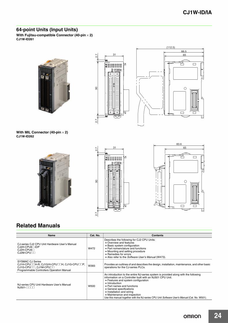
CJ1W-ID/IA
24
64-point Units (Input Units)With Fujitsu-compatible Connector (40-pin × 2)CJ1W-ID261
With MIL Connector (40-pin × 2)CJ1W-ID262
Related Manuals
Name Cat. No. Contents
CJ-series CJ2 CPU Unit Hardware User’s ManualCJ2H-CPU6@-EIPCJ2H-CPU6@CJ2M-CPU@@
W472
Describes the following for CJ2 CPU Units:• Overview and features• Basic system configuration• Part nomenclature and functions• Mounting and setting procedure• Remedies for errors• Also refer to the Software User’s Manual (W473).
SYSMAC CJ SeriesCJ1H-CPU@@H-R, CJ1G/H-CPU@@H, CJ1G-CPU@@P, CJ1G-CPU@@, CJ1M-CPU@@Programmable Controllers Operation Manual
W393 Provides an outlines of and describes the design, installation, maintenance, and other basic operations for the CJ-series PLCs.
NJ-series CPU Unit Hardware User's Manual NJ501-@@@@ W500
An introduction to the entire NJ-series system is provided along with the following information on a Controller built with an NJ501 CPU Unit.• Features and system configuration• Introduction• Part names and functions• General specifications• Installation and wiring• Maintenance and inspection
Use this manual together with the NJ-series CPU Unit Software User's Manual (Cat. No. W501).
6566.5
(112.5)
902.
72.
7
31
83.665
902.
7 31
2.7

Terms and Conditions Agreement Read and understand this catalog. Please read and understand this catalog before purchasing the products. Please consult your OMRON representative if you have any questions or comments. Warranties. (a) Exclusive Warranty. Omron’s exclusive warranty is that the Products will be free from defects in materials and workmanship for a period of twelve months from the date of sale by Omron (or such other period expressed in writing by Omron). Omron disclaims all other warranties, express or implied. (b) Limitations. OMRON MAKES NO WARRANTY OR REPRESENTATION, EXPRESS OR IMPLIED, ABOUT NON-INFRINGEMENT, MERCHANTABILITY OR FITNESS FOR A PARTICULAR PURPOSE OF THE PRODUCTS. BUYER ACKNOWLEDGES THAT IT ALONE HAS DETERMINED THAT THE PRODUCTS WILL SUITABLY MEET THE REQUIREMENTS OF THEIR INTENDED USE. Omron further disclaims all warranties and responsibility of any type for claims or expenses based on infringement by the Products or otherwise of any intellectual property right. (c) Buyer Remedy. Omron’s sole obligation hereunder shall be, at Omron’s election, to (i) replace (in the form originally shipped with Buyer responsible for labor charges for removal or replacement thereof) the non-complying Product, (ii) repair the non-complying Product, or (iii) repay or credit Buyer an amount equal to the purchase price of the non-complying Product; provided that in no event shall Omron be responsible for warranty, repair, indemnity or any other claims or expenses regarding the Products unless Omron’s analysis confirms that the Products were properly handled, stored, installed and maintained and not subject to contamination, abuse, misuse or inappropriate modification. Return of any Products by Buyer must be approved in writing by Omron before shipment. Omron Companies shall not be liable for the suitability or unsuitability or the results from the use of Products in combination with any electrical or electronic components, circuits, system assemblies or any other materials or substances or environments. Any advice, recommendations or information given orally or in writing, are not to be construed as an amendment or addition to the above warranty. See http://www.omron.com/global/ or contact your Omron representative for published information. Limitation on Liability; Etc. OMRON COMPANIES SHALL NOT BE LIABLE FOR SPECIAL, INDIRECT, INCIDENTAL, OR CONSEQUENTIAL DAMAGES, LOSS OF PROFITS OR PRODUCTION OR COMMERCIAL LOSS IN ANY WAY CONNECTED WITH THE PRODUCTS, WHETHER SUCH CLAIM IS BASED IN CONTRACT, WARRANTY, NEGLIGENCE OR STRICT LIABILITY. Further, in no event shall liability of Omron Companies exceed the individual price of the Product on which liability is asserted. Suitability of Use. Omron Companies shall not be responsible for conformity with any standards, codes or regulations which apply to the combination of the Product in the Buyer’s application or use of the Product. At Buyer’s request, Omron will provide applicable third party certification documents identifying ratings and limitations of use which apply to the Product. This information by itself is not sufficient for a complete determination of the suitability of the Product in combination with the end product, machine, system, or other application or use. Buyer shall be solely responsible for determining appropriateness of the particular Product with respect to Buyer’s application, product or system. Buyer shall take application responsibility in all cases. NEVER USE THE PRODUCT FOR AN APPLICATION INVOLVING SERIOUS RISK TO LIFE OR PROPERTY OR IN LARGE QUANTITIES WITHOUT ENSURING THAT THE SYSTEM AS A WHOLE HAS BEEN DESIGNED TO ADDRESS THE RISKS, AND THAT THE OMRON PRODUCT(S) IS PROPERLY RATED AND INSTALLED FOR THE INTENDED USE WITHIN THE OVERALL EQUIPMENT OR SYSTEM. Programmable Products. Omron Companies shall not be responsible for the user’s programming of a programmable Product, or any consequence thereof. Performance Data. Data presented in Omron Company websites, catalogs and other materials is provided as a guide for the user in determining suitability and does not constitute a warranty. It may represent the result of Omron’s test conditions, and the user must correlate it to actual application requirements. Actual performance is subject to the Omron’s Warranty and Limitations of Liability. Change in Specifications. Product specifications and accessories may be changed at any time based on improvements and other reasons. It is our practice to change part numbers when published ratings or features are changed, or when significant construction changes are made. However, some specifications of the Product may be changed without any notice. When in doubt, special part numbers may be assigned to fix or establish key specifications for your application. Please consult with your Omron’s representative at any time to confirm actual specifications of purchased Product. Errors and Omissions. Information presented by Omron Companies has been checked and is believed to be accurate; however, no responsibility is assumed for clerical, typographical or proofreading errors or omissions.
2014.4
In the interest of product improvement, specifications are subject to change without notice.
OMRON Corporation Industrial Automation Company http://www.ia.omron.com/
(c)Copyright OMRON Corporation 2014 All Right Reserved.

CSM_CJ1W-OUTPUT_DS_E_7_1
1
CJ-series Output Units
CJ1W-OC/OA/ODA Wide Range of Basic Output Units for High Speed Output and Different Applications
• These Output Units receive the results of output instructions from the CPU Unit and perform ON/OFF control for external devices.
• High-speed Output models CJ1W-OD213 and CJ1W-OD234 can help to increase system throughput.
Features• High-speed output models are available, meeting versatile applications.
ON Response Time: 15μs, OFF Response Time: 80μs• Output Units are available with any of three output types: relay contact outputs, triac outputs, or transistor outputs.• For transistor outputs, select from sinking outputs or sourcing outputs. • Output Units with load short-circuit protection are also available. *1• Select the best interface for each application: Fujitsu connectors or MIL connectors. *2• A wide variety of Connector-Terminal Block Conversion Units are available to allow you to easily wire external output devices.
*1. The following Units have load short-circuit protection: CJ1W-OC202, CJ1W-OD204, CJ1W-OD212, and CJ1W-OD232.*2. Available for models with 32 outputs or 64 outputs
CJ1W-OD213 CJ1W-OD234

CJ1W-OC/OA/OD
2
Ordering InformationInternational Standards• The standards are abbreviated as follows: U: UL, U1: UL (Class I Division 2 Products for Hazardous Locations), C: CSA, UC: cULus, UC1: cULus (Class I Division 2
Products for Hazardous Locations), CU: cUL, N: NK, L: Lloyd, and CE: EC Directives.• Contact your OMRON representative for further details and applicable conditions for these standards.
Output Units
AccessoriesConnectors are not included for models with connectors. Either use one of the applicable connector listed below or use an applicable Connector-Terminal Block Conversion Unit or I/O Relay Terminal. For details on wiring methods, refer to External Interface.
Unit type Product name
Specifications No. of words
allocated
Current consumption
(A) Model StandardsOutput
typeI/O
pointsMaximum switching
capacity Commons External connection 5 V 24 V
CJ1 Basic I/O Units
Relay Contact Output Units
− 8 outputs
250 VAC/24 VDC, 2 AIndependent contacts
Removable terminal block
1 words 0.090.048 max.
CJ1W-OC201
UC1, N, L, CE
− 16 outputs 250 VAC/24 VDC, 2 A
16 points, 1 common
Removable terminal block
1 words 0.110.096 max. CJ1W-OC211
Triac Output Unit
− 8 outputs 250 VAC, 0.6 A 8 points,
1 common
Removable terminal block
1 words 0.22 − CJ1W-OA201
Transistor Output Units
Sinking 8 outputs 12 to 24 VDC, 2 A 4 points,
1 common
Removable terminal block
1 words 0.09 − CJ1W-OD201
Sinking 8 outputs 12 to 24 VDC, 0.5 A 8 points,
1 common
Removable terminal block
1 words 0.10 − CJ1W-OD203
Sinking 16 outputs 12 to 24 VDC, 0.5 A 16 points,
1 common
Removable terminal block
1 words 0.10 − CJ1W-OD211
Sinking
16outputs(High
speed)
24 VDC, 0.5 A 16 points, 1 common
Removable terminal block
1 words 0.15 − CJ1W-OD213 N, L, CE
Sinking 32 outputs 12 to 24 VDC, 0.5 A 16 points,
1 commonFujitsu connector 2 words 0.14 − CJ1W-OD231
UC1, N, L, CE
Sinking 32 outputs 12 to 24 VDC, 0.5 A 16 points,
1 commonMIL connector 2 words 0.14 − CJ1W-OD233
Sinking
32 outputs(High
speed)
24 VDC, 0.5 A 16 points, 1 common
MIL connector 2 words 0.22 − CJ1W-OD234 N, L, CE
Sinking 64 outputs 12 to 24 VDC, 0.3 A 16 points,
1 commonFujitsu connector 4 words 0.17 − CJ1W-OD261
UC1, N, L, CE
Sinking 64 outputs
12 to 24 VDC, 0.3 A 16 points, 1 common
MIL connector 4 words 0.17 − CJ1W-OD263
Sourcing8
outputs24 VDC, 2 AShort-circuit protection
4 points, 1 common
Removable terminal block
1 words 0.11 − CJ1W-OD202
Sourcing 8 outputs
24 VDC, 0.5 AShort-circuit protection
8 points, 1 common
Removable terminal block
1 words 0.10 − CJ1W-OD204
Sourcing 16 outputs
24 VDC, 0.5 AShort-circuit protection
16 points, 1 common
Removable terminal block
1 words 0.10 − CJ1W-OD212
Sourcing 32outputs
24 VDC, 0.5 AShort-circuit protection
16 points, 1 common
MIL connector 2 words 0.15 − CJ1W-OD232
Sourcing 64 outputs 12 to 24 VDC, 0.3 A 16 points,
1 commonMIL connector 4 words 0.17 − CJ1W-OD262

3
CJ1W-OC/OA/OD
Applicable ConnectorsFujitsu Connectors for 32-input, 32-output, 64-input, 64-output, 32-input/32-output, and 16-input/16-output Units
MIL Connectors for 32-input, 32-output, 64-input, 64-output, 32-input/32-output, and 16-input/16-output Units
* Crimp Contacts are also required. Refer to page 31 for details.
Applicable Connector-Terminal Block Conversion Units
Note: For the combination of Output Units with Connector-Terminal Block Conversion Units, refer to 2. Connecting Connector-Terminal Block Conversion Units.
Name Connection Remarks Applicable Units Model Standards
40-pin Connectors
SolderedFCN-361J040-AU ConnectorFCN-360C040-J2 Connector Cover
Fujitsu Connectors: CJ1W-ID231(32 inputs): 1 per UnitCJ1W-ID261 (64 inputs): 2 per UnitCJ1W-OD231 (32 outputs): 1 per UnitCJ1W-OD261 (64 outputs): 2 per UnitCJ1W-MD261 (32 inputs, 32 outputs): 2 per Unit
C500-CE404
−
CrimpedFCN-363J040 HousingFCN-363J-AU ContactorFCN-360C040-J2 Connector Cover
C500-CE405
Pressure welded FCN-367J040-AU/F C500-CE403
24-pin Connectors
Soldered FCN-361J024-AU ConnectorFCN-360C024-J2 Connector Cover
Fujitsu Connectors:CJ1W-MD231 (16 inputs, 16 outputs): 2 per Unit
C500-CE241
CrimpedFCN-363J024 HousingFCN-363J-AU ContactorFCN-360C024-J2 Connector Cover
C500-CE242
Pressure welded FCN-367J024-AU/F C500-CE243
Name Connection Remarks Applicable Units Model Standards
40-pin Connectors
Pressure welded FRC5-AO40-3TOSMIL Connectors:CJ1W-ID232/233 (32 inputs): 1 per UnitCJ1W-OD232/233/234 (32 outputs):1 per UnitCJ1W-ID262 (64 inputs): 2 per UnitCJ1W-OD262/263 (64 outputs): 2 per UnitCJ1W-MD263/563 (32 inputs, 32 outputs): 2 per Unit
XG4M-4030-T
−
Crimped − XG5N-401*
20-pin Connectors
Pressure welded FRC5-AO20-3TOS MIL Connectors:CJ1W-MD232/233 (16 inputs, 16 outputs): 2 per Unit
XG4M-2030-T−
Crimped − XG5N-201*
Type Series I/O Number of poles Wiring method Terminal
type
Size MountingCommon terminals
Bleeder resistance Indicators I/O Units Model StandardsDepth
(mm)Height (mm)
Width (mm)
DIN Track Screws
PLCs XW2R Output 34
Phillips screw
M3 50 48.35 130.7
Yes Yes No No No
CJ1W-OD231CJ1W-OD261
XW2R-J34G-C3
−
CJ1W-OD232CJ1W-OD233CJ1W-OD234CJ1W-OD262CJ1W-OD263
XW2R-J34G-C4
Slotted screw (rise up)
M3(Europeantype)
50 45.11 98.5
CJ1W-OD231CJ1W-OD261
XW2R-E34G-C3
CJ1W-OD232CJ1W-OD233CJ1W-OD234CJ1W-OD262CJ1W-OD263
XW2R-E34G-C4
Push-in spring
Clamp 50 45.11 98.5
CJ1W-OD231CJ1W-OD261
XW2R-P34G-C3
CJ1W-OD232CJ1W-OD233CJ1W-OD234CJ1W-OD262CJ1W-OD263
XW2R-P34G-C4

CJ1W-OC/OA/OD
4
Applicable I/O Relay Terminals
Note: For the combination of Output Units with I/O Relay Terminal and Connecting Cables, refer to 3. Connecting I/O Relay Terminals.
Type Series
Specifications Size (horizontal mounting) Mounting
Model StandradsClassification Polarity
Number of
points
Rated ON current at contacts
Operation indicators
Terminal block for
power supply wiring
Horizontal (mm)
Vertical (mm)
Height (mm)
DIN Track Screws
Space-saving G70D
Vertical typeG70D-V
Outputs
Relay outputs
NPN16 (SPST-NO × 16)
5A or 3A
Yes Expandable 135 46 81 Yes Yes
G70D-VSOC16U, C, CEMOSFET
relay outputs
0.3A G70D-VFOM16
Flat typeG70D
Relay outputs
NPN
8 (SPST-NO × 8) 5A
Yes −
68 93 44
Yes Yes
G70D-SOC08 −
16 (SPST-NO × 16)
3A
156 51 39
G70D-SOC16
−
PNP16 (SPST-NO × 16)
3A G70D-SOC16-1
MOSFET relay outputs
NPN 16 (SPST-NO × 16)
0.3AG70D-FOM16
−PNP G70D-FOM16-1
High-capacity, space-saving
G70R Outputs Relay outputs NPN 8 (SPST-
NO × 8) 10A Yes − 136 93 55 Yes Yes G70R-SOC08 −
Standard G7TC
Inputs
AC inputs
NPN16 (SPST-NO × 16)
1A
Yes −
182
85 68 Yes −
G7TC-IA16
U, C
DC inputs
G7TC-ID16
Outputs Relay outputs
NPN
8 (SPST-NO × 8)
5A
102 G7TC-OC08
16 (SPST-NO × 16)
182
G7TC-OC16
PNP16 (SPST-NO × 16)
G7TC-OC16-1 −
High-capacity socket
G70A (Socket only) Outputs Relay
outputs
NPN 16 (SPDT × 16 possible with G2R Relays)
10 A (Terminal block allowable current)
No − 234 75 64 Yes −
G70A-ZOC16-3
U, C, CE
(Socket only) + Relay/SSR/MOSFET Relay/Timer
PNP
G70A-ZOC16-4(Socket only) + Relay/SSR/MOSFET Relay/Timer

5
CJ1W-OC/OA/OD
Mountable Racks
ModelNJ system CJ system (CJ1, CJ2) CP1H system NSJ system
CPU Rack Expansion Rack CPU Rack Expansion Backplane CP1H PLC NSJ Controller Expansion
Backplane
CJ1W-OC201
10 Units10 Units
(Per Expansion Rack)
10 Units10 Units
(Per Expansion Backplane)
Not Supported Not Supported10 Units
(Per Expansion Backplane)
CJ1W-OC211
CJ1W-OA201
CJ1W-OD201
CJ1W-OD203
CJ1W-OD211
CJ1W-OD213
CJ1W-OD231
CJ1W-OD233
CJ1W-OD234
CJ1W-OD261
CJ1W-OD263
CJ1W-OD202
CJ1W-OD204
CJ1W-OD212
CJ1W-OD232
CJ1W-OD262

CJ1W-OC/OA/OD
6
SpecificationsCJ1W-OC201 Contact Output Unit (Independent Relays, 8 Points)
* Terminal numbers A0 to A8 and B0 to B8 are used in the external connection and terminal-device variable diagrams. They are not printed on the Units.
Note: Although 16 I/O bits (1 word) are allocated, only 8 of these can be used for external I/O.
Name 8-point Contact Output Unit with Terminal Block (Independent Relays)
Model CJ1W-OC201
Max. Switching Capacity 2 A 250 VAC (cosφ = 1), 2 A 250 VAC (cosφ = 0.4), 2 A 24 VDC (16 A/Unit)
Min. Switching Capacity 1 mA 5 VDC
Relays NY-24W-K-IE (Fujitsu Takamizawa Components, Ltd.), Cannot be replaced.
Service Life of RelayElectrical: 150,000 operations (24 VDC, resistive load)/100,000 operations (240 VAC, cosφ = 0.4, inductive load) Mechanical: 20,000,000 operationsService life will vary depending on the connected load.
ON Response Time 15 ms max.
OFF Response Time 15 ms max.
Number of Circuits 8 independent contacts
Insulation Resistance 20 MΩ between external terminals and the GR terminal (500 VDC)
Dielectric Strength 2,000 VAC between the external terminals and the GR terminal for 1 minute at a leakage current of 10 mA max.
Internal Current Consumption
90 mA 5 VDC max. 48 mA 24 VDC max. (6 mA × No. of ON points)
Weight 140 g max.
Circuit Configuration
• The signal names of the terminals are the device variable names.The device variable names are the names that use "Jxx" as the device name.
External connection and terminal-device variable diagram
• The signal names of the terminals are the device variable names.The device variable names are the names that use "Jxx" as the device name.
• The input power supply polarity can be connected in either direction.
Output indicator
Inte
rnal
circ
uits
Signal name
Jxx_Ch1_Out00
Jxx_Ch1_Out00
2 A 250 VAC, 2 A 24 VDC max.
Signal name
Signal name
Connec-tor pin *
B1
B2
B3
B4
B5
B6
B7
B8
A1
A2
A3
A4
A5
A6
A7
A8
B0A0
L
L
L
L
L
L
L
L
Jxx_Ch1_Out00
Jxx_Ch1_Out01
Jxx_Ch1_Out02
Jxx_Ch1_Out03
Jxx_Ch1_Out04
Jxx_Ch1_Out05
Jxx_Ch1_Out06
Jxx_Ch1_Out07
NC
Jxx_Ch1_Out00
Jxx_Ch1_Out01
Jxx_Ch1_Out02
Jxx_Ch1_Out03
Jxx_Ch1_Out04
Jxx_Ch1_Out05
Jxx_Ch1_Out06
Jxx_Ch1_Out07
NC

7
CJ1W-OC/OA/OD
CJ1W-OC211 Contact Output Unit (16 Points)
* Terminal numbers A0 to A8 and B0 to B8 are used in the external connection and terminal-device variable diagrams. They are not printed on the Units.
Name 16-point Contact Output Unit with Terminal Block
Model CJ1W-OC211
Max. Switching Capacity 2 A 250 VAC (cosφ = 1), 2 A 250 VAC (cosφ = 0.4), 2 A 24 VDC (8 A/Unit)
Min. Switching Capacity 1 mA 5 VDC
Relays NY-24W-K-IE (Fujitsu Takamizawa Components, Ltd.), Cannot be replaced.
Service Life of RelayElectrical: 150,000 operations (24 VDC, resistive load)/ 100,000 operations (250 VAC, cosφ = 0.4, inductive load) Mechanical: 20,000,000 operationsService life will vary depending on the connected load.
ON Response Time 15 ms max.
OFF Response Time 15 ms max.
Number of Circuits 16 points/common, 1 circuit
Insulation Resistance 20 MΩ between external terminals and the GR terminal (500 VDC)
Dielectric Strength 2,000 VAC between the external terminals and the GR terminal for 1 minute at a leakage current of 10 mA max.
Internal Current Consumption
110 mA 5 VDC max. 96 mA 24 VDC max. (6 mA × No. of ON points)
Weight 170 g max.
Circuit Configuration
• The signal names of the terminals are the device variable names.The device variable names are the names that use "Jxx" as the device name.
External connection and terminal-device variable diagram
• The signal names of the terminals are the device variable names.The device variable names are the names that use "Jxx" as the device name.
Output indicator
Inte
rnal
circ
uits
to
Signal name
Jxx_Ch1_Out15
Jxx_Ch1_Out00
COM
COM
2 A 250 VAC, 2 A 24 VDC max.
Signal name
Signal name
Connec-tor pin *
B1
B2
B3
B4
B5
B6
B7
B8
A1
A2
A3
A4
A5
A6
A7
A8
B0A0L
L
L
L
L
L
L
L
L
L
L
L
L
L
L
L
Jxx_Ch1_Out01
Jxx_Ch1_Out03
Jxx_Ch1_Out05
Jxx_Ch1_Out07
Jxx_Ch1_Out09
Jxx_Ch1_Out11
Jxx_Ch1_Out13
Jxx_Ch1_Out15
Jxx_Ch1_Out00
Jxx_Ch1_Out02
Jxx_Ch1_Out04
Jxx_Ch1_Out06
Jxx_Ch1_Out08
Jxx_Ch1_Out10
Jxx_Ch1_Out12
Jxx_Ch1_Out14
COM
COM

CJ1W-OC/OA/OD
8
CJ1W-OA201 Triac Output Unit (8 Points)
* Terminal numbers A0 to A8 and B0 to B8 are used in the external connection and terminal-device variable diagrams. They are not printed on the Units.
Note: Although 16 I/O bits (1 word) are allocated, only 8 of these can be used for external I/O.
Name 8-point Triac Output Unit with Terminal Block
Model CJ1W-OA201
Max. Switching Capacity 0.6 A 250 VAC, 50/60 Hz (2.4 A/Unit)
Max. Inrush Current 15 A (pulse width: 10 ms max.)
Min. Switching Capacity 50 mA 75 VAC
Leakage Current 1.5 mA (200 VAC) max.
Residual Voltage 1.6 VAC max.
ON Response Time 1 ms max.
OFF Response Time 1/2 of load frequency + 1 ms or less.
Number of Circuits 8 (8 points/common, 1 circuit)
Surge Protector C.R Absorber + Surge Absorber
Fuses 5 A (1/common, 1 used)The fuse cannot be replaced by the user.
Insulation Resistance 20 MΩ between the external terminals and the GR terminal (500 VDC)
Dielectric Strength 2,000 VAC between the external terminals and the GR terminal for 1 minute at a leakage current of 10 mA max.
Internal Current Consumption 220 mA max.
Weight 150 g max.
Circuit Configuration
• The signal names of the terminals are the device variable names.The device variable names are the names that use "Jxx" as the device name.
External connection and terminal-device variable diagram
• The signal names of the terminals are the device variable names.The device variable names are the names that use "Jxx" as the device name.
Output indicator
Inte
rnal
circ
uits
Fuse
to
Signal name
COM
Jxx_Ch1_Out00
Jxx_Ch1_Out07
250 VAC max.
Signal name
Connec-tor pin *
B0
B1
B2
B3
B4
B5
B6
B7
B8
A0
A1
A2
A3
A4
A5
A6
A7
A8
NC
NC
NC
NC
NC
NC
NC
NC
NC
L
L
L
L
L
L
L
LCOM
Jxx_Ch1_Out00
Jxx_Ch1_Out01
Jxx_Ch1_Out02
Jxx_Ch1_Out03
Jxx_Ch1_Out04
Jxx_Ch1_Out05
Jxx_Ch1_Out06
Jxx_Ch1_Out07

9
CJ1W-OC/OA/OD
CJ1W-OD201 Transistor Output Unit (8 Points)
* Terminal numbers A0 to A8 and B0 to B8 are used in the external connection and terminal-device variable diagrams. They are not printed on the Units.
Note: Although 16 I/O bits (1 word) are allocated, only 8 of these can be used for external I/O.
Name 8-point Transistor Output Unit with Terminal Block (Sinking Outputs)
Model CJ1W-OD201
Rated Voltage 12 to 24 VDC
Operating Load Voltage Range 10.2 to 26.4 VDC
Maximum Load Current 2.0 A/point, 8.0 A/Unit
Maximum Inrush Current 10 A/point, 10 ms max.
Leakage Current 0.1 mA max.
Residual Voltage 1.5 V max.
ON Response Time 0.5 ms max.
OFF Response Time 1.0 ms max.
Insulation Resistance 20 MΩ between the external terminals and the GR terminal (100 VDC)
Dielectric Strength 1,000 VAC between the external terminals and the GR terminal for 1 minute at a leakage current of 10 mA max.
Number of Circuits 8 (4 points/common, 2 circuits)
Internal Current Consumption 90 mA max.
Fuse 6.3 A (1/common, 2 used)The fuse cannot be replaced by the user.
External Power Supply 12 to 24 VDC, 10 mA min.
Weight 110 g max.
Circuit Configuration
• The signal names of the terminals are the device variable names.The device variable names are the names that use "Jxx" as the device name.
External connection and terminal-device variable diagram
• When wiring, pay careful attention to the polarity of the external power supply. The load may operate incorrectly if the polarity is reversed.• The signal names of the terminals are the device variable names.
The device variable names are the names that use "Jxx" as the device name.
Inte
rnal
circ
uits
Output indicator
Fuse
Fuse
to
to
Signal name
Jxx_Ch1_Out00
+V
Jxx_Ch1_Out03
COM0
Jxx_Ch1_Out04
+V
Jxx_Ch1_Out07
COM1
12 to 24 VDC
12 to 24 VDC
Signal name
Signal name
Connec-tor pin *
B0
B1
B2
B3
B4
B5
B6
B7
B8
A0
A1
A2
A3
A4
A5
A6
A7
A8
L
L
L
LL
L
L
LJxx_Ch1_Out00
Jxx_Ch1_Out02
COM0
NC
NC
Jxx_Ch1_Out04
Jxx_Ch1_Out06
NC
Jxx_Ch1_Out01
Jxx_Ch1_Out03
+V
NC
NC
NC
Jxx_Ch1_Out05
Jxx_Ch1_Out07
COM1
+V

CJ1W-OC/OA/OD
10
CJ1W-OD203 Transistor Output Unit (8 Points)
* Terminal numbers A0 to A8 and B0 to B8 are used in the external connection and terminal-device variable diagrams. They are not printed on the Units.
Note: Although 16 I/O bits (1 word) are allocated, only 8 of these can be used for external I/O.
Name 8-point Transistor Output Unit with Terminal Block (Sinking Outputs)
Model CJ1W-OD203
Rated Voltage 12 to 24 VDC
Operating Load Voltage Range 10.2 to 26.4 VDC
Maximum Load Current 0.5 A/point, 4.0 A/Unit
Maximum Inrush Current 4.0 A/point, 10 ms max.
Leakage Current 0.1 mA max.
Residual Voltage 1.5 V max.
ON Response Time 0.1 ms max.
OFF Response Time 0.8 ms max.
Insulation Resistance 20 MΩ between the external terminals and the GR terminal (100 VDC)
Dielectric Strength 1,000 VAC between the external terminals and the GR terminal for 1 minute at a leakage current of 10 mA max.
Number of Circuits 8 (8 points/common, 1 circuit)
Internal Current Consumption 100 mA max.
Fuse None
External Power Supply 10.2 to 26.4 VDC, 20 mA min.
Weight 110 g max.
Circuit Configuration
• The signal names of the terminals are the device variable names.The device variable names are the names that use "Jxx" as the device name.
External connection and terminal-device variable diagram
• When wiring, pay careful attention to the polarity of the external power supply. The load may operate incorrectly if the polarity is reversed.• The signal names of the terminals are the device variable names.
The device variable names are the names that use "Jxx" as the device name.
Output indicator
Inte
rnal
circ
uits
to
Signal name
Jxx_Ch1_Out00
Jxx_Ch1_Out07
+V
COM
12 to 24 VDC
Signal name
Signal name
Connec-tor pin *
B1
B2
B3
B4
B5
B6
B7
B8
A1
A2
A3
A4
A5
A6
A7
A8
B0A0L
L
L
L
L
L
L
L
Jxx_Ch1_Out01
Jxx_Ch1_Out03
Jxx_Ch1_Out05
Jxx_Ch1_Out07
Jxx_Ch1_Out00
Jxx_Ch1_Out02
Jxx_Ch1_Out04
Jxx_Ch1_Out06
NC
COM+V
NC
NC
NC
NC
NC
NC
NC

11
CJ1W-OC/OA/OD
CJ1W-OD211 Transistor Output Unit (16 Points)
* Terminal numbers A0 to A8 and B0 to B8 are used in the external connection and terminal-device variable diagrams. They are not printed on the Units.
Name 16-point Transistor Output Unit with Terminal Block (Sinking Outputs)
Model CJ1W-OD211
Rated Voltage 12 to 24 VDC
Operating Load Voltage Range 10.2 to 26.4 VDC
Maximum Load Current 0.5 A/point, 5.0 A/Unit
Maximum Inrush Current 4.0 A/point, 10 ms max.
Leakage Current 0.1 mA max.
Residual Voltage 1.5 V max.
ON Response Time 0.1 ms max.
OFF Response Time 0.8 ms max.
Insulation Resistance 20 MΩ between the external terminals and the GR terminal (100 VDC)
Dielectric Strength 1,000 VAC between the external terminals and the GR terminal for 1 minute at a leakage current of 10 mA max.
Number of Circuits 16 (16 points/common, 1 circuit)
Internal Current Consumption 5 VDC 100 mA max.
Fuse None
External Power Supply 10.2 to 26.4 VDC, 20 mA min.
Weight 110 g max.
Circuit Configuration
• The signal names of the terminals are the device variable names.The device variable names are the names that use "Jxx" as the device name.
External connection and terminal-device variable diagram
• When wiring, pay careful attention to the polarity of the external power supply. The load may operate incorrectly if the polarity is reversed.• The signal names of the terminals are the device variable names.
The device variable names are the names that use "Jxx" as the device name.
Output indicator
Inte
rnal
circ
uits
to
Signal name
Jxx_Ch1_Out00
+V
Jxx_Ch1_Out15
COM
12 to 24 VDC
Signal name
Signal name
Connec-tor pin *
B1
B2
B3
B4
B5
B6
B7
B8
A1
A2
A3
A4
A5
A6
A7
A8
B0A0L
L
L
L
L
L
L
L
L
L
L
L
L
L
L
L
Jxx_Ch1_Out01
Jxx_Ch1_Out03
Jxx_Ch1_Out05
Jxx_Ch1_Out07
Jxx_Ch1_Out09
Jxx_Ch1_Out11
Jxx_Ch1_Out13
Jxx_Ch1_Out15
Jxx_Ch1_Out00
Jxx_Ch1_Out02
Jxx_Ch1_Out04
Jxx_Ch1_Out06
Jxx_Ch1_Out08
Jxx_Ch1_Out10
Jxx_Ch1_Out12
Jxx_Ch1_Out14
COM+V

CJ1W-OC/OA/OD
12
CJ1W-OD213 Transistor Output Unit (16 Points)
* Terminal numbers A0 to A8 and B0 to B8 are used in the external connection and terminal-device variable diagrams. They are not printed on the Units.
Name 16-point Transistor Output Unit with Terminal Block (Sinking Outputs)
Model CJ1W-OD213
Rated Voltage 24 VDC
Operating Load Voltage Range 20.4 to 26.4 VDC
Maximum Load Current 0.5 A/point, 5.0 A/Unit
Maximum Inrush Current 4.0 A/point, 10 ms max.
Leakage Current 0.1 mA max.
Residual Voltage 1.5 V max.
ON Response Time 15 μs max.
OFF Response Time 80 μs max.
Insulation Resistance 20 MΩ between the external terminals and the GR terminal (100 VDC)
Dielectric Strength 1,000 VAC between the external terminals and the GR terminal for 1 minute at a leakage current of 10 mA max.
Number of Circuits 16 (16 points/common, 1 circuit)
Internal Current Consumption 5 VDC 150 mA max.
Fuse None
External Power Supply 20.4 to 26.4 VDC, 55 mA min.
Weight 110 g max.
Circuit Configuration
• The signal names of the terminals are the device variable names.The device variable names are the names that use "Jxx" as the device name.
External connection and terminal-device variable diagram
• When wiring, pay careful attention to the polarity of the external power supply. The load may operate incorrectly if the polarity is reversed.• The signal names of the terminals are the device variable names.
The device variable names are the names that use "Jxx" as the device name.
Output indicator
Inte
rnal
circ
uits to
Signal name
Jxx_Ch1_Out00
+V
Jxx_Ch1_Out15
COM
24 VDC
Signal name
Signal name
Connec-tor pin *
B1
B2
B3
B4
B5
B6
B7
B8
A1
A2
A3
A4
A5
A6
A7
A8
B0A0L
L
L
L
L
L
L
L
L
L
L
L
L
L
L
L
Jxx_Ch1_Out01
Jxx_Ch1_Out03
Jxx_Ch1_Out05
Jxx_Ch1_Out07
Jxx_Ch1_Out09
Jxx_Ch1_Out11
Jxx_Ch1_Out13
Jxx_Ch1_Out15
Jxx_Ch1_Out00
Jxx_Ch1_Out02
Jxx_Ch1_Out04
Jxx_Ch1_Out06
Jxx_Ch1_Out08
Jxx_Ch1_Out10
Jxx_Ch1_Out12
Jxx_Ch1_Out14
COM+V

13
CJ1W-OC/OA/OD
CJ1W-OD231 Transistor Output Unit (32 Points)Name 32-point Transistor Output Unit with Fujitsu Connector (Sinking Outputs) Model CJ1W-OD231Rated Voltage 12 to 24 VDCOperating Load Voltage Range 10.2 to 26.4 VDC
Maximum Load Current 0.5 A/point, 2.0 A/common, 4.0 A/Unit
Maximum Inrush Current 4.0 A/point, 10 ms max.
Leakage Current 0.1 mA max.Residual Voltage 1.5 V max.ON Response Time 0.1 ms max.OFF Response Time 0.8 ms max.Insulation Resistance 20 MΩ between the external terminals and the GR terminal (100 VDC)Dielectric Strength 1,000 VAC between the external terminals and the GR terminal for 1 minute at a leakage current of 10 mA max.Number of Circuits 32 (16 points/common, 2 circuits)Internal Current Consumption 5 VDC 140 mA max.
Fuse NoneExternal Power Supply 10.2 to 26.4 VDC, 30 mA min.
Weight 70 g max.Accessories None
Circuit Configuration
• The signal names of the terminals are the device variable names.The device variable names are the names that use "Jxx" as the device name.
External connection and terminal-device variable diagram
• When wiring, pay careful attention to the polarity of the external power supply. The load may operate incorrectly if the polarity is reversed.• Be sure to wire both terminals A9 and A19 (COM0).• Be sure to wire both terminals B9 and B19 (COM1).• Be sure to wire both terminals A10 and A20 (+V).• Be sure to wire both terminals B10 and B20 (+V).• The signal names of the terminals are the device variable names.
The device variable names are the names that use "Jxx" as the device name.
Output indicator
to
to
Inte
rnal
circ
uits
Wd m+1
Wd m
Allocated CIO word
Signal name
Connector row A
Connector row B
Jxx_Ch1_Out00
+V
Jxx_Ch1_Out15
COM0
Jxx_Ch2_Out00
+V
Jxx_Ch2_Out15
COM1
COM0
COM1
SW
Wd m+1
Wd m+1
Wd m
Wd m
12 to 24 VDC
12 to 24 VDC
Signal name
Signal name
Connec-tor pin Allocated
CIO wordAllocated CIO word
L
L
L
L
L
L
L
L
L
L
L
L
L
L
L
L
L
L
L
L
L
L
L
L
L
L
L
L
L
L
L
L
A1
A2
A3
A4
A5
A6
A7
A8
A9
A10
A11
A12
A13
A14
A15
A16
A17
A18
A19
A20
B1
B2
B3
B4
B5
B6
B7
B8
B9
B10
B11
B12
B13
B14
B15
B16
B17
B18
B19
B20
+V
COM0
+V
COM0
Jxx_Ch1_Out08
Jxx_Ch1_Out09
Jxx_Ch1_Out10
Jxx_Ch1_Out11
Jxx_Ch1_Out12
Jxx_Ch1_Out13
Jxx_Ch1_Out14
Jxx_Ch1_Out15
Jxx_Ch1_Out00
Jxx_Ch1_Out01
Jxx_Ch1_Out02
Jxx_Ch1_Out03
Jxx_Ch1_Out04
Jxx_Ch1_Out05
Jxx_Ch1_Out06
Jxx_Ch1_Out07
COM1
+V
COM1
+V
Jxx_Ch2_Out08
Jxx_Ch2_Out09
Jxx_Ch2_Out10
Jxx_Ch2_Out11
Jxx_Ch2_Out12
Jxx_Ch2_Out13
Jxx_Ch2_Out14
Jxx_Ch2_Out15
Jxx_Ch2_Out00
Jxx_Ch2_Out01
Jxx_Ch2_Out02
Jxx_Ch2_Out03
Jxx_Ch2_Out04
Jxx_Ch2_Out05
Jxx_Ch2_Out06
Jxx_Ch2_Out07

CJ1W-OC/OA/OD
14
CJ1W-OD233 Transistor Output Unit (32 Points)Name 32-point Transistor Output Unit with MIL Connector (Sinking Outputs)Model CJ1W-OD233Rated Voltage 12 to 24 VDCOperating Load Voltage Range 10.2 to 26.4 VDC
Maximum Load Current 0.5 A/point, 2 A/common, 4 A/Unit
Maximum Inrush Current 4.0 A/point, 10 ms max.
Leakage Current 0.1 mA max.Residual Voltage 1.5 V max.ON Response Time 0.1 ms max.OFF Response Time 0.8 ms max.Insulation Resistance 20 MΩ between the external terminals and the GR terminal (100 VDC)Dielectric Strength 1,000 VAC between the external terminals and the GR terminal for 1 minute at a leakage current of 10 mA max.Number of Circuits 32 (16 points/common, 2 circuits)Internal Current Consumption 140 mA max.
Fuse NoneExternal Power Supply 12 to 24 VDC, 30 mA min.
Weight 70 g max.
Circuit Configuration
• The signal names of the terminals are the device variable names.The device variable names are the names that use "Jxx" as the device name.
External connection and terminal-device variable diagram
• When wiring, pay careful attention to the polarity of the external power supply. The load may operate incorrectly if the polarity is reversed.• Be sure to wire both terminals 23 and 24 (COM0).• Be sure to wire both terminals 3 and 4 (COM1).• Be sure to wire both terminals 21 and 22 (+V).• Be sure to wire both terminals 1 and 2 (+V).• The signal names of the terminals are the device variable names.
The device variable names are the names that use "Jxx" as the device name.
Wd m+1
Wd m to
to
Output indicator
Inte
rnal
circ
uits
Allocated CIO word
Signal name
Jxx_Ch1_Out00
+V
Jxx_Ch1_Out15
COM0
Jxx_Ch2_Out00
+V
Jxx_Ch2_Out15
COM1
COM0
COM1
SW
Wd
m+
1W
d m
Wd
m+
1W
d m
12 to 24 VDC
12 to 24 VDC
Signal name
Signal name
Connec-tor pin
Allocated CIO word
Allocated CIO word
40
38
36
34
32
30
28
26
24
22
20
18
16
14
12
10
8
6
4
2
39
37
35
33
31
29
27
25
23
21
19
17
15
13
11
9
7
5
3
1
L
L
L
L
L
L
L
L
L
L
L
L
L
L
L
L
L
L
L
L
L
L
L
L
L
L
L
L
L
L
L
L
Jxx_Ch2_Out00
Jxx_Ch2_Out01
Jxx_Ch2_Out02
Jxx_Ch2_Out03
Jxx_Ch2_Out04
Jxx_Ch2_Out05
Jxx_Ch2_Out06
+VCOM1
Jxx_Ch2_Out08
Jxx_Ch2_Out09
Jxx_Ch2_Out10
Jxx_Ch2_Out11
Jxx_Ch2_Out12
Jxx_Ch2_Out07
Jxx_Ch2_Out13
Jxx_Ch2_Out14
Jxx_Ch2_Out15
+V COM1
+V +V
Jxx_Ch1_Out00
Jxx_Ch1_Out01
Jxx_Ch1_Out02
Jxx_Ch1_Out03
Jxx_Ch1_Out04
Jxx_Ch1_Out05
Jxx_Ch1_Out06
Jxx_Ch1_Out07
Jxx_Ch1_Out08
Jxx_Ch1_Out09
Jxx_Ch1_Out10
Jxx_Ch1_Out11
Jxx_Ch1_Out12
Jxx_Ch1_Out13
Jxx_Ch1_Out14
Jxx_Ch1_Out15
COM0 COM0

15
CJ1W-OC/OA/OD
CJ1W-OD234 Transistor Output Unit (32 Points)Name 32-point Transistor Output Unit with MIL Connector (Sinking Outputs)Model CJ1W-OD234Rated Voltage 24 VDCOperating Load Voltage Range 20.4 to 26.4 VDC
Maximum Load Current 0.5 A/point, 2 A/common, 4 A/Unit
Maximum Inrush Current 4.0 A/point, 10 ms max.
Leakage Current 0.1 mA max.Residual Voltage 1.5 V max.ON Response Time 15 μs max.OFF Response Time 80 μs max.Insulation Resistance 20 MΩ between the external terminals and the GR terminal (100 VDC)Dielectric Strength 1,000 VAC between the external terminals and the GR terminal for 1 minute at a leakage current of 10 mA max.Number of Circuits 32 (16 points/common, 2 circuits)Internal Current Consumption 220 mA max.
Fuse NoneExternal Power Supply 20.4 to 26.4 VDC, 110 mA min.
Weight 70 g max.
Circuit Configuration
• The signal names of the terminals are the device variable names.The device variable names are the names that use "Jxx" as the device name.
External connection and terminal-device variable diagram
• When wiring, pay careful attention to the polarity of the external power supply. The load may operate incorrectly if the polarity is reversed.• Be sure to wire both terminals 23 and 24 (COM0).• Be sure to wire both terminals 3 and 4 (COM1).• Be sure to wire both terminals 21 and 22 (+V).• Be sure to wire both terminals 1 and 2 (+V).• The signal names of the terminals are the device variable names.
The device variable names are the names that use "Jxx" as the device name.
Wd m+1
Wd m to
to
Output indicator
Inte
rnal
circ
uits
Allocated CIO word
Signal name
Jxx_Ch1_Out00+V
Jxx_Ch1_Out15
COM0
Jxx_Ch2_Out00+V
Jxx_Ch2_Out15
COM1
COM0
COM1
SW
Wd
m+
1W
d m
Wd
m+
1W
d m
24 VDC
24 VDC
Signal name
Signal name
Connec-tor pin
Allocated CIO word
Allocated CIO word
40
38
36
34
32
30
28
26
24
22
20
18
16
14
12
10
8
6
4
2
39
37
35
33
31
29
27
25
23
21
19
17
15
13
11
9
7
5
3
1
L
L
L
L
L
L
L
L
L
L
L
L
L
L
L
L
L
L
L
L
L
L
L
L
L
L
L
L
L
L
L
L
Jxx_Ch2_Out00
Jxx_Ch2_Out01
Jxx_Ch2_Out02
Jxx_Ch2_Out03
Jxx_Ch2_Out04
Jxx_Ch2_Out05
Jxx_Ch2_Out06
+VCOM1
Jxx_Ch2_Out08
Jxx_Ch2_Out09
Jxx_Ch2_Out10
Jxx_Ch2_Out11
Jxx_Ch2_Out12
Jxx_Ch2_Out07
Jxx_Ch2_Out13
Jxx_Ch2_Out14
Jxx_Ch2_Out15
+V COM1
+V +V
Jxx_Ch1_Out00
Jxx_Ch1_Out01
Jxx_Ch1_Out02
Jxx_Ch1_Out03
Jxx_Ch1_Out04
Jxx_Ch1_Out05
Jxx_Ch1_Out06
Jxx_Ch1_Out07
Jxx_Ch1_Out08
Jxx_Ch1_Out09
Jxx_Ch1_Out10
Jxx_Ch1_Out11
Jxx_Ch1_Out12
Jxx_Ch1_Out13
Jxx_Ch1_Out14
Jxx_Ch1_Out15
COM0 COM0

CJ1W-OC/OA/OD
16
CJ1W-OD261 Transistor Output Unit (64 Points)Name 64-point Transistor Output Unit with Fujitsu Connectors (Sinking Outputs)
Model CJ1W-OD261
Rated Voltage 12 to 24 VDC
Operating Load Voltage Range 10.2 to 26.4 VDC
Maximum Load Current 0.3 A/point, 1.6 A/common, 6.4 A/Unit
Maximum Inrush Current 3.0 A/point, 10 ms max.
Leakage Current 0.1 mA max.
Residual Voltage 1.5 V max.
ON Response Time 0.5 ms max.
OFF Response Time 1.0 ms max.
Insulation Resistance 20 MΩ between the external terminals and the GR terminal (100 VDC)
Dielectric Strength 1,000 VAC between the external terminals and the GR terminal for 1 minute at a leakage current of 10 mA max.
Number of Circuits 64 (16 points/common, 4 circuits)
Internal Current Consumption 5 VDC, 170 mA max.
Fuse None
External Power Supply 10.2 to 26.4 VDC, 50 mA min.
Weight 110 g max.
Accessories None
Circuit Configuration
• The signal names of the terminals are the device variable names.The device variable names are the names that use "Jxx" as the device name.
Output indicator
to
to
to
to
Wd m
Wd m+1
Wd m+2
Wd m+3
Inte
rnal
circ
uits
Allocated CIO word
Signal name
Connector row A
Connector row B
Connector row A
Connector row B
Jxx_Ch1_Out00
+V
Jxx_Ch1_Out15COM0
Jxx_Ch3_Out00
+V
Jxx_Ch3_Out15
COM2
COM0
COM2
+VJxx_Ch2_Out00
Jxx_Ch2_Out15COM1COM1
+VJxx_Ch4_Out00
Jxx_Ch4_Out15COM3COM3
CN1
SW
CN2

CJ1W-OC/OA/OD
17
External connection and terminal-device variable diagram
CN1 CN2
• When wiring, pay careful attention to the polarity of the external power supply. The load may operate incorrectly if the polarity is reversed.
• Be sure to wire both terminals A9 and A19 (COM0) of CN1.• Be sure to wire both terminals B9 and B19 (COM1) of CN1.• Be sure to wire both terminals A10 and A20 (+V) of CN1.• Be sure to wire both terminals B10 and B20 (+V) of CN1.• The signal names of the terminals are the device variable
names.The device variable names are the names that use "Jxx" as the device name.
• When wiring, pay careful attention to the polarity of the external power supply. The load may operate incorrectly if the polarity is reversed.
• Be sure to wire both terminals A9 and A19 (COM2) of CN2.• Be sure to wire both terminals B9 and B19 (COM3) of CN2.• Be sure to wire both terminals A10 and A20 (+V) of CN2.• Be sure to wire both terminals B10 and B20 (+V) of CN2.• The signal names of the terminals are the device variable
names.The device variable names are the names that use "Jxx" as the device name.
12 to 24 VDC
Wd
m
Wd
m+
1
12 to 24 VDCW
d m
+1
Wd
m
Signal name
Signal name
Connec-tor pin
Allocated CIO word
Allocated CIO word
COM0
+V
COM0
+V
COM1
+V
Jxx_Ch2_Out08
Jxx_Ch2_Out09
Jxx_Ch2_Out10
Jxx_Ch2_Out11
Jxx_Ch2_Out12
Jxx_Ch2_Out13
Jxx_Ch2_Out14
Jxx_Ch2_Out15
COM1
+V
L
L
L
L
L
L
L
L
L
L
L
L
L
L
L
L
L
L
L
L
L
L
L
L
L
L
L
L
L
L
L
LJxx_Ch2_Out00
Jxx_Ch2_Out01
Jxx_Ch2_Out02
Jxx_Ch2_Out03
Jxx_Ch2_Out04
Jxx_Ch2_Out05
Jxx_Ch2_Out06
Jxx_Ch2_Out07
Jxx_Ch1_Out00
Jxx_Ch1_Out01
Jxx_Ch1_Out02
Jxx_Ch1_Out03
Jxx_Ch1_Out04
Jxx_Ch1_Out05
Jxx_Ch1_Out06
Jxx_Ch1_Out07
Jxx_Ch1_Out08
Jxx_Ch1_Out09
Jxx_Ch1_Out10
Jxx_Ch1_Out11
Jxx_Ch1_Out12
Jxx_Ch1_Out13
Jxx_Ch1_Out14
Jxx_Ch1_Out15
A20
A19
A18
A17
A16
A15
A14
A13
A12
A11
A10
A9
A8
A7
A6
A5
A4
A3
A2
A1
B20
B19
B18
B17
B16
B15
B14
B13
B12
B11
B10
B9
B8
B7
B6
B5
B4
B3
B2
B1
12 to 24 VDC
Wd
m+
3
Wd
m+
2W
d m
+2
Wd
m+
3
12 to 24 VDC
Signal name
Signal name
Connec-tor pin Allocated
CIO wordAllocated CIO word
L
L
L
L
L
L
L
L
L
L
L
L
L
L
L
L
L
L
L
L
L
L
L
L
L
L
L
L
L
L
L
L
A1
A2
A3
A4
A5
A6
A7
A8
A9
A10
A11
A12
A13
A14
A15
A16
A17
A18
A19
A20
B1
B2
B3
B4
B5
B6
B7
B8
B9
B10
B11
B12
B13
B14
B15
B16
B17
B18
B19
B20
COM3
+V
COM3
+V
COM2
+V
Jxx_Ch3_Out08
Jxx_Ch3_Out09
Jxx_Ch3_Out10
Jxx_Ch3_Out11
Jxx_Ch3_Out12
Jxx_Ch3_Out13
Jxx_Ch3_Out14
Jxx_Ch3_Out15
COM2
+V
Jxx_Ch3_Out00
Jxx_Ch3_Out01
Jxx_Ch3_Out02
Jxx_Ch3_Out03
Jxx_Ch3_Out04
Jxx_Ch3_Out05
Jxx_Ch3_Out06
Jxx_Ch3_Out07
Jxx_Ch4_Out00
Jxx_Ch4_Out01
Jxx_Ch4_Out02
Jxx_Ch4_Out03
Jxx_Ch4_Out04
Jxx_Ch4_Out05
Jxx_Ch4_Out06
Jxx_Ch4_Out07
Jxx_Ch4_Out08
Jxx_Ch4_Out09
Jxx_Ch4_Out10
Jxx_Ch4_Out11
Jxx_Ch4_Out12
Jxx_Ch4_Out13
Jxx_Ch4_Out14
Jxx_Ch4_Out15

CJ1W-OC/OA/OD
18
CJ1W-OD263 Transistor Output Unit (64 Points)Name 64-point Transistor Output Unit with MIL Connectors (Sinking Outputs)
Model CJ1W-OD263
Rated Voltage 12 to 24 VDC
Operating Load Voltage Range 10.2 to 26.4 VDC
Maximum Load Current 0.3 A/point, 1.6 A/common, 6.4 A/Unit
Maximum Inrush Current 3.0 A/point, 10 ms max.
Leakage Current 0.1 mA max.
Residual Voltage 1.5 V max.
ON Response Time 0.5 ms max.
OFF Response Time 1.0 ms max.
Insulation Resistance 20 MΩ between the external terminals and the GR terminal (100 VDC)
Dielectric Strength 1,000 VAC between the external terminals and the GR terminal for 1 minute at a leakage current of 10 mA max.
Number of Circuits 64 (16 points/common, 4 circuits)
Internal Current Consumption 170 mA max.
Fuse None
External Power Supply 12 to 24 VDC, 50 mA min.
Weight 110 g max.
Circuit Configuration
• The signal names of the terminals are the device variable names.The device variable names are the names that use "Jxx" as the device name.
Inte
rnal
circ
uits
Output indicator
to Wd m
Wd m+1
Wd m+2
Wd m+3
Allocated CIO word
Signal name
Jxx_Ch1_Out00
+V
Jxx_Ch1_Out15COM0
Jxx_Ch3_Out00
+V
Jxx_Ch3_Out15
COM2
COM0
COM2
+VJxx_Ch2_Out00
Jxx_Ch2_Out15COM1COM1
+VJxx_Ch4_Out00
Jxx_Ch4_Out15COM3COM3
CN1
SW
CN2
to
to
to

CJ1W-OC/OA/OD
19
External connection and terminal-device variable diagram
CN1 CN2
• When wiring, pay careful attention to the polarity of the external power supply. The load may operate incorrectly if the polarity is reversed.
• Be sure to wire both terminals 23 and 24 (COM0) of CN1.• Be sure to wire both terminals 3 and 4 (COM1) of CN1.• Be sure to wire both terminals 21 and 22 (+V) of CN1.• Be sure to wire both terminals 1 and 2 (+V) of CN1.• The signal names of the terminals are the device variable
names.The device variable names are the names that use "Jxx" as the device name.
• When wiring, pay careful attention to the polarity of the external power supply. The load may operate incorrectly if the polarity is reversed.
• Be sure to wire both terminals 23 and 24 (COM2) of CN2.• Be sure to wire both terminals 3 and 4 (COM3) of CN2.• Be sure to wire both terminals 21 and 22 (+V) of CN2.• Be sure to wire both terminals 1 and 2 (+V) of CN2.• The signal names of the terminals are the device variable
names.The device variable names are the names that use "Jxx" as the device name.
Wd
m
Wd
mW
d m
+1
Wd
m+
1
12 to 24 VDC
12 to 24 VDC
Signal name
Signal name
Connec-tor pin
Allocated CIO word
Allocated CIO word
1
3
5
7
9
11
13
15
17
19
21
23
25
27
29
31
33
35
37
39
2
4
6
8
10
12
14
16
18
20
22
24
26
28
30
32
34
36
38
40L
L
L
L
L
L
L
L
L
L
L
L
L
L
L
L
L
L
L
L
L
L
L
L
L
L
L
L
L
L
L
L
+V
Jxx_Ch1_Out15
Jxx_Ch1_Out14
Jxx_Ch1_Out13
Jxx_Ch1_Out12
Jxx_Ch1_Out11
+V
+V
COM1
Jxx_Ch1_Out10
COM1
+V
Jxx_Ch1_Out00
Jxx_Ch1_Out07
Jxx_Ch1_Out06
Jxx_Ch1_Out05
Jxx_Ch1_Out04
Jxx_Ch1_Out03
Jxx_Ch1_Out02
Jxx_Ch1_Out01
COM0
Jxx_Ch1_Out08
Jxx_Ch1_Out09
COM0
Jxx_Ch2_Out15
Jxx_Ch2_Out14
Jxx_Ch2_Out13
Jxx_Ch2_Out12
Jxx_Ch2_Out11
Jxx_Ch2_Out10
Jxx_Ch2_Out08
Jxx_Ch2_Out09
Jxx_Ch2_Out00
Jxx_Ch2_Out07
Jxx_Ch2_Out06
Jxx_Ch2_Out05
Jxx_Ch2_Out04
Jxx_Ch2_Out03
Jxx_Ch2_Out02
Jxx_Ch2_Out01
Wd
m+
3
Wd
m+
3W
d m
+2
Wd
m+
2
12 to 24 VDC
12 to 24 VDC
Signal name
Signal name
Connec-tor pin
Allocated CIO word
Allocated CIO word
40
38
36
34
32
30
28
26
24
22
20
18
16
14
12
10
8
6
4
2
39
37
35
33
31
29
27
25
23
21
19
17
15
13
11
9
7
5
3
1
L
L
L
L
L
L
L
L
L
L
L
L
L
L
L
L
L
L
L
L
L
L
L
L
L
L
L
L
L
L
L
L
+V
COM3
+V
COM3
+V +V
COM2 COM2
Jxx_Ch4_Out08
Jxx_Ch4_Out09
Jxx_Ch4_Out10
Jxx_Ch4_Out11
Jxx_Ch4_Out12
Jxx_Ch4_Out13
Jxx_Ch4_Out14
Jxx_Ch4_Out15
Jxx_Ch3_Out08
Jxx_Ch3_Out09
Jxx_Ch3_Out10
Jxx_Ch3_Out11
Jxx_Ch3_Out12
Jxx_Ch3_Out13
Jxx_Ch3_Out14
Jxx_Ch3_Out15
Jxx_Ch4_Out00
Jxx_Ch4_Out01
Jxx_Ch4_Out02
Jxx_Ch4_Out03
Jxx_Ch4_Out04
Jxx_Ch4_Out05
Jxx_Ch4_Out06
Jxx_Ch4_Out07
Jxx_Ch3_Out00
Jxx_Ch3_Out01
Jxx_Ch3_Out02
Jxx_Ch3_Out03
Jxx_Ch3_Out04
Jxx_Ch3_Out05
Jxx_Ch3_Out06
Jxx_Ch3_Out07

CJ1W-OC/OA/OD
20
CJ1W-OD202 Transistor Output Unit (8 Points)
* Terminal numbers A0 to A8 and B0 to B8 are used in the external connection and terminal-device variable diagrams. They are not printed on the Units.
Note: Although 16 I/O bits (1 word) are allocated, only 8 of these can be used for external I/O.
Name 8-point Transistor Output Unit with Terminal Block (Sourcing Outputs)
Model CJ1W-OD202
Rated Voltage 24 VDC
Operating Load Voltage Range 20.4 to 26.4 VDC
Maximum Load Current 2 A/point, 8 A/Unit
Leakage Current 0.1 mA max.
Residual Voltage 1.5 V max.
ON Response Time 0.5 ms max.
OFF Response Time 1.0 ms max.
Load Short-circuit Protection
Detection current: 6 A min.Automatic restart after error clearance.
Line Disconnection Detection Detection current: 200 mA
Insulation Resistance 20 MΩ between the external terminals and the GR terminal (100 VDC)
Dielectric Strength 1,000 VAC between the external terminals and the GR terminal for 1 minute at a leakage current of 10 mA max.
Number of Circuits 8 (4 points/common, 2 circuits)
Internal Current Consumption 110 mA max.
Fuse None
External Power Supply 24 VDC, 50 mA min.
Weight 120 g max.
Circuit Configuration
• When overcurrent or line disconnection is detected, the ERR indicator will light, and the corresponding bit (two points per bit) in the Basic I/O Unit Information Area (A050 to A069) will change to TRUE.
• The signal names of the terminals are the device variable names.The device variable names are the names that use "Jxx" as the device name.
External connection and terminal-device variable diagram
• When wiring, pay careful attention to the polarity of the external power supply. The load may operate incorrectly if the polarity is reversed.• The signal names of the terminals are the device variable names.
The device variable names are the names that use "Jxx" as the device name.
COM0 (+V)
COM1 (+V)
to
to
Output indicator
ERR indicator
Inte
rnal
circ
uits
Signal name
Jxx_Ch1_Out03
Jxx_Ch1_Out00
0 V
Jxx_Ch1_Out04
Jxx_Ch1_Out070 V
Sho
rt-c
ircui
t pr
otec
tion
Sho
rt-c
ircui
t pr
otec
tion
24 VDC
24 VDC
Signal name
Signal name
Connec-tor pin*
B0
B1
B2
B3
B4
B5
B6
B7
B8
A0
A1
A2
A3
A4
A5
A6
A7
A8
L
L
L
L
L
L
L
L
Jxx_Ch1_Out00
Jxx_Ch1_Out02
0 V
NC
NC
Jxx_Ch1_Out04
Jxx_Ch1_Out06
NC
Jxx_Ch1_Out01
Jxx_Ch1_Out03
COM0 (+V)
NC
NC
NC
Jxx_Ch1_Out05
Jxx_Ch1_Out07
0 V COM1 (+V)

21
CJ1W-OC/OA/OD
CJ1W-OD204 Transistor Output Unit (8 Points)
* Terminal numbers A0 to A8 and B0 to B8 are used in the external connection and terminal-device variable diagrams. They are not printed on the Units.
Note: Although 16 I/O bits (1 word) are allocated, only 8 of these can be used for external I/O.
Name 8-point Transistor Output Unit with Terminal Block (Sourcing Outputs)
Model CJ1W-OD204
Rated Voltage 24 VDC
Operating Load Voltage Range 20.4 to 26.4 VDC
Maximum Load Current 0.5 A/point, 4.0 A/Unit
Leakage Current 0.1 mA max.
Residual Voltage 1.5 V max.
ON Response Time 0.5 ms max.
OFF Response Time 1.0 ms max.
Load Short-circuit Protection
Detection current: 0.7 to 2.5 AAutomatic restart after error clearance.
Insulation Resistance 20 MΩ between the external terminals and the GR terminal (100 VDC)
Dielectric Strength 1,000 VAC between the external terminals and the GR terminal for 1 minute at a leakage current of 10 mA max.
Number of Circuits 8 (8 points/common, 1 circuit)
Internal Current Consumption 5 VDC, 100 mA max.
Fuse None
External Power Supply 20.4 to 26.4 VDC, 40 mA min.
Weight 120 g max.
Circuit Configuration
• When overcurrent is detected, the ERR indicator will light, and the corresponding bit in the Basic I/O Unit Information Area (A050 to A069) will change to TRUE.
• The signal names of the terminals are the device variable names.The device variable names are the names that use "Jxx" as the device name.
External connection and terminal-device variable diagram
• When wiring, pay careful attention to the polarity of the external power supply. The load may operate incorrectly if the polarity is reversed.• The signal names of the terminals are the device variable names.
The device variable names are the names that use "Jxx" as the device name.
Output indicator
ERR indicator
Inte
rnal
circ
uits to
Signal name
COM (+V)
Jxx_Ch1_Out00
Jxx_Ch1_Out070 V
Sho
rt-c
ircui
t pr
otec
tion
24 VDC
Signal name
Signal name
Connec-tor pin *
B1
Jxx_Ch1_Out01
B2
Jxx_Ch1_Out03
B3
Jxx_Ch1_Out05
B4
Jxx_Ch1_Out07
B5
B6
B7
B8
A1
Jxx_Ch1_Out00
A2
Jxx_Ch1_Out02
A3
Jxx_Ch1_Out04
A4
Jxx_Ch1_Out06
A5
NC
A6
A7
A80 V
B0A0
COM (+V)
L
L
L
L
L
L
L
L
NC
NC
NC
NC
NC
NC
NC

CJ1W-OC/OA/OD
22
CJ1W-OD212 Transistor Output Unit (16 Points)
* Terminal numbers A0 to A8 and B0 to B8 are used in the external connection and terminal-device variable diagrams. They are not printed on the Units.
Name 16-point Transistor Output Unit with Terminal Block (Sourcing Outputs)
Model CJ1W-OD212
Rated Voltage 24 VDC
Operating Load Voltage Range 20.4 to 26.4 VDC
Maximum Load Current 0.5 A/point, 5.0 A/Unit
Maximum Inrush Current 0.1 mA max.
Leakage Current 1.5 V max.
ON Response Time 0.5 ms max.
OFF Response Time 1.0 ms max.
Load Short-circuit Protection
Detection current: 0.7 to 2.5 AAutomatic restart after error clearance.
Insulation Resistance 20 MΩ between the external terminals and the GR terminal (100 VDC)
Dielectric Strength 1,000 VAC between the external terminals and the GR terminal for 1 minute at a leakage current of 10 mA max.
Number of Circuits 16 (16 points/common, 1 circuit)
Internal Current Consumption 5 VDC, 100 mA max.
External Power Supply 20.4 to 26.4 VDC, 40 mA min.
Weight 120 g max.
Circuit Configuration
• When overcurrent is detected, the ERR indicator will light, and the corresponding bit in the Basic I/O Unit Information Area (A050 to A069) will change to TRUE.
• The signal names of the terminals are the device variable names.The device variable names are the names that use "Jxx" as the device name.
External connection and terminal-device variable diagram
• When wiring, pay careful attention to the polarity of the external power supply. The load may operate incorrectly if the polarity is reversed.• The signal names of the terminals are the device variable names.
The device variable names are the names that use "Jxx" as the device name.
Inte
rnal
circ
uits
Output indicator
ERR indicator
to
Signal name
Jxx_Ch1_Out15
Jxx_Ch1_Out00
0 V
COM (+V)
Sho
rt-c
ircui
t pr
otec
tion
24 VDC
Signal name
Signal name
Connector pin *
B1
B2
B3
B4
B5
B6
B7
B8
A1
A2
A3
A4
A5
A6
A7
A8
B0A0L
L
L
L
L
L
L
L
L
L
L
L
L
L
L
L
Jxx_Ch1_Out01
Jxx_Ch1_Out03
Jxx_Ch1_Out05
Jxx_Ch1_Out07
Jxx_Ch1_Out09
Jxx_Ch1_Out11
Jxx_Ch1_Out13
Jxx_Ch1_Out15
Jxx_Ch1_Out00
Jxx_Ch1_Out02
Jxx_Ch1_Out04
Jxx_Ch1_Out06
Jxx_Ch1_Out08
Jxx_Ch1_Out10
Jxx_Ch1_Out12
Jxx_Ch1_Out14
0 VCOM (+V)

23
CJ1W-OC/OA/OD
CJ1W-OD232 Transistor Output Unit (32 Points)Name 32-point Transistor Output Unit with MIL Connector (Sourcing Outputs)
Model CJ1W-OD232
Rated Voltage 24 VDC
Operating Load Voltage Range 20.4 to 26.4 VDC
Maximum Load Current 0.5 A/point, 2.0 A/common, 4.0 A/Unit
Leakage Current 0.1 mA max.
Residual Voltage 1.5 V max.
ON Response Time 0.5 ms max.
OFF Response Time 1.0 ms max.
Load Short-circuit Protection
Detection current: 0.7 to 2.5 AAutomatic restart after error clearance.
Insulation Resistance 20 MΩ between the external terminals and the GR terminal (100 VDC)
Dielectric Strength 1,000 VAC between the external terminals and the GR terminal for 1 minute at a leakage current of 10 mA max.
Number of Circuits 32 (16 points/common, 2 circuits)
Internal Current Consumption 5 VDC 150 mA max.
External Power Supply 20.4 to 26.4 VDC, 70 mA min.
Weight 80 g max.
Accessories None
Circuit Configuration
• When overcurrent is detected, the ERR indicator will light, and the corresponding bit (bit allocated for each common) in the Basic I/O Unit Information Area (A050 to A069) will change to TRUE.
• The signal names of the terminals are the device variable names. The device variable names are the names that use "Jxx" as the device name.
Wd m
Wd m+1
to
to
Output indicator
Inte
rnal
circ
uits
ERR indicator
Allocated CIO word
Signal name
Jxx_Ch1_Out15Jxx_Ch1_Out00
0 V
Jxx_Ch2_Out00Jxx_Ch2_Out150 V
SW
COM0 (+V)COM0 (+V)
COM1 (+V)COM1 (+V)
Sho
rt-c
ircui
t pr
otec
tion
Sho
rt-c
ircui
t pr
otec
tion

24
CJ1W-OC/OA/OD
External connection and terminal-device variable diagram
• When wiring, pay careful attention to the polarity of the external power supply. The load may operate incorrectly if the polarity is reversed.• Be sure to wire both terminals 21 and 22 (COM0 (+V)). • Be sure to wire both terminals 1 and 2 (COM1 (+V)).• Be sure to wire both terminals 3 and 4 (0 V).• Be sure to wire both terminals 23 and 24 (0 V).• The signal names of the terminals are the device variable names.
The device variable names are the names that use "Jxx" as the device name.
Wd
m+
1
Wd
m+
1
Wd
m
Wd
m
24 VDC
24 VDC
Signal name
Signal name
Connec-tor pin
Allocated CIO word
Allocated CIO word
40
38
36
34
32
30
28
26
24
22
20
18
16
14
12
10
8
6
4
2
39
37
35
33
31
29
27
25
23
21
19
17
15
13
11
9
7
5
3
1
L
L
L
L
L
L
L
L
L
L
L
L
L
L
L
L
L
L
L
L
L
L
L
L
L
L
L
L
L
L
L
L
Jxx_Ch2_Out00
Jxx_Ch2_Out01
Jxx_Ch2_Out02
Jxx_Ch2_Out03
Jxx_Ch2_Out04
Jxx_Ch2_Out05
Jxx_Ch2_Out06
Jxx_Ch2_Out07
0 V
COM1 (+V)
Jxx_Ch2_Out08
Jxx_Ch2_Out09
Jxx_Ch2_Out10
Jxx_Ch2_Out11
Jxx_Ch2_Out12
Jxx_Ch2_Out13
Jxx_Ch2_Out14
Jxx_Ch2_Out15
0 V
COM1 (+V)
0 V
COM0 (+V)
0 V
COM0 (+V)
Jxx_Ch1_Out00
Jxx_Ch1_Out01
Jxx_Ch1_Out02
Jxx_Ch1_Out03
Jxx_Ch1_Out04
Jxx_Ch1_Out05
Jxx_Ch1_Out06
Jxx_Ch1_Out07
Jxx_Ch1_Out08
Jxx_Ch1_Out09
Jxx_Ch1_Out10
Jxx_Ch1_Out11
Jxx_Ch1_Out12
Jxx_Ch1_Out13
Jxx_Ch1_Out14
Jxx_Ch1_Out15

25
CJ1W-OC/OA/OD
CJ1W-OD262 Transistor Output Unit (64 Points)Name 64-point Transistor Output Unit with MIL Connectors (Sourcing Outputs)
Model CJ1W-OD262
Rated Voltage 12 to 24 VDC
Operating Load Voltage Range 10.2 to 26.4 VDC
Maximum Load Current 0.3 A/point, 1.6 A/common, 6.4 A/Unit
Maximum Inrush Current 3.0 A/point, 10 ms max.
Leakage Current 0.1 mA max.
Residual Voltage 1.5 V max.
ON Response Time 0.5 ms max.
OFF Response Time 1.0 ms max.
Insulation Resistance 20 MΩ between the external terminals and the GR terminal (100 VDC)
Dielectric Strength 1,000 VAC between the external terminals and the GR terminal for 1 minute at a leakage current of 10 mA max.
Number of Circuits 64 (16 points/common, 4 circuits)
Internal Current Consumption 170 mA max. (5 VDC)
Fuse None
External Power Supply 10.2 to 26.4 VDC, 50 mA min.
Weight 110 g max.
Accessories None
Circuit Configuration
• The signal names of the terminals are the device variable names.The device variable names are the names that use "Jxx" as the device name.
Wd m
Wd m+1
Wd m+3
Wd m+2
Inte
rnal
circ
uits Indicator switch
Output indicator
to
to
to
to
Allocated CIO word
Signal name
Jxx_Ch1_Out150 V
Jxx_Ch1_Out00
COM0COM0
0 V
0 V
COM1
0 V
COM1
Jxx_Ch2_Out15
Jxx_Ch2_Out00
COM2COM2
Jxx_Ch3_Out15
Jxx_Ch3_Out00
Jxx_Ch4_Out15
Jxx_Ch4_Out00
COM3COM3
CN1 (OUT)
CN2 (OUT)

CJ1W-OC/OA/OD
26
External connection and terminal-device variable diagram
CN1 CN2
• When wiring, pay careful attention to the polarity of the external power supply. The load may operate incorrectly if the polarity is reversed.
• Be sure to wire both terminals 21 and 22 (COM0 (+V)) of CN1. • Be sure to wire both terminals 1 and 2 (COM1 (+V)) of CN1.• Be sure to wire both terminals 23 and 24 (0 V) of CN1.• Be sure to wire both terminals 3 and 4 (0 V) of CN1.• The signal names of the terminals are the device variable
names.The device variable names are the names that use "Jxx" as the device name.
• When wiring, pay careful attention to the polarity of the external power supply. The load may operate incorrectly if the polarity is reversed.
• Be sure to wire both terminals 21 and 22 (COM2 (+V)) of CN2. • Be sure to wire both terminals 1 and 2 (COM3 (+V)) of CN2.• Be sure to wire both terminals 23 and 24 (0 V) of CN2.• Be sure to wire both terminals 3 and 4 (0 V) of CN2.• The signal names of the terminals are the device variable
names.The device variable names are the names that use "Jxx" as the device name.
Wd
m12 to
24 VDCW
d m
+1
Wd
mW
d m
+1
12 to 24 VDC
Signal name
Signal name
Connec-tor pin
Allocated CIO word
Allocated CIO word
13
5
7
9
11
13
15
17
19
21
23
25
27
29
31
33
35
37
39
24
6
8
10
12
14
16
18
20
22
24
26
28
30
32
34
36
38
40L L
L L
L L
L L
L L
L L
L L
L L
L L
L L
L L
L L
L L
L L
L L
L LJxx_Ch2_Out15
Jxx_Ch2_Out14
Jxx_Ch2_Out13
Jxx_Ch2_Out12
Jxx_Ch2_Out11
Jxx_Ch2_Out10Jxx_Ch2_Out02
Jxx_Ch1_Out15
Jxx_Ch1_Out14
Jxx_Ch1_Out13
Jxx_Ch1_Out12
Jxx_Ch1_Out11
0 V
0 V
Jxx_Ch2_Out07
Jxx_Ch2_Out06
Jxx_Ch2_Out05
Jxx_Ch2_Out04
Jxx_Ch2_Out03
COM1 (+V)
Jxx_Ch1_Out10
0 V
Jxx_Ch1_Out00
Jxx_Ch1_Out07
Jxx_Ch1_Out06
Jxx_Ch1_Out05
Jxx_Ch1_Out04
Jxx_Ch1_Out03
Jxx_Ch1_Out02
Jxx_Ch1_Out01
COM0 (+V)
Jxx_Ch1_Out08
Jxx_Ch1_Out09
COM0 (+V)
Jxx_Ch2_Out08
Jxx_Ch2_Out09
Jxx_Ch2_Out00
Jxx_Ch2_Out01
0 V
COM1 (+V)
Wd
m+
3W
d m
+2
12 to 24 VDC
12 to 24 VDC
Wd
m+
3W
d m
+2
Signal name
Signal name
Connector pin
Allocated CIO word
Allocated CIO word
L L
L L
L L
L L
L L
L L
L L
L L
L L
L L
L L
L L
40
38
36
34
32
30
28
26
24
22
20
18
16
14
12
10
8
6
4
2
39
37
35
33
31
29
27
25
23
21
19
17
15
13
10
9
7
5
3
1
LL
L L
L
L L
LJxx_Ch3_Out00
Jxx_Ch3_Out01
Jxx_Ch3_Out02
Jxx_Ch3_Out03
Jxx_Ch3_Out04
Jxx_Ch3_Out05
Jxx_Ch3_Out06
Jxx_Ch3_Out07Jxx_Ch3_Out15
Jxx_Ch4_Out00
Jxx_Ch4_Out01
Jxx_Ch4_Out02
Jxx_Ch4_Out03
Jxx_Ch4_Out04
Jxx_Ch4_Out05
Jxx_Ch4_Out06
Jxx_Ch3_Out08
Jxx_Ch3_Out09
Jxx_Ch3_Out10
Jxx_Ch3_Out11
Jxx_Ch3_Out12
Jxx_Ch3_Out13
Jxx_Ch3_Out14
Jxx_Ch4_Out08
Jxx_Ch4_Out09
Jxx_Ch4_Out10
Jxx_Ch4_Out11
Jxx_Ch4_Out12
Jxx_Ch4_Out07
Jxx_Ch4_Out13
Jxx_Ch4_Out14
Jxx_Ch4_Out15
0 V
COM3 (+V)
0 V
COM2 (+V)
0 V
COM3 (+V)
0 V
COM2 (+V)

27
CJ1W-OC/OA/OD
Bit Allocations for Output Unit8-point Output Unit 16-point Output Unit
32-point Output Unit 64-point Output Unit
Allocated CIO wordSignal name (CJ/NJ)
CIO Bit
Wd m(Output)
00 OUT0/Jxx_Ch1_Out00
01 OUT1/Jxx_Ch1_Out01
: :
06 OUT6/Jxx_Ch1_Out06
07 OUT7/Jxx_Ch1_Out07
08 −
09 −
: :
14 −
15 −
Allocated CIO wordSignal name (CJ/NJ)
CIO Bit
Wd m(Output)
00 OUT0/Jxx_Ch1_Out00
01 OUT1/Jxx_Ch1_Out01
: :
14 OUT14/Jxx_Ch1_Out14
15 OUT15/Jxx_Ch1_Out15
Allocated CIO wordSignal name (CJ/NJ)
CIO Bit
Wd m(Output)
00 OUT0/Jxx_Ch1_Out00
01 OUT1/Jxx_Ch1_Out01
: :
14 OUT14/Jxx_Ch1_Out14
15 OUT15/Jxx_Ch1_Out15
Wd m+1(Output)
00 OUT0/Jxx_Ch2_Out00
01 OUT1/Jxx_Ch2_Out01
: :
14 OUT14/Jxx_Ch2_Out14
15 OUT15/Jxx_Ch2_Out15
Allocated CIO wordSignal name (CJ/NJ)
CIO Bit
Wd m(Output)
00 OUT0/Jxx_Ch1_Out00
01 OUT1/Jxx_Ch1_Out01
: :
14 OUT14/Jxx_Ch1_Out14
15 OUT15/Jxx_Ch1_Out15
Wd m+1(Output)
00 OUT0/Jxx_Ch2_Out00
01 OUT1/Jxx_Ch2_Out01
: :
14 OUT14/Jxx_Ch2_Out14
15 OUT15/Jxx_Ch2_Out15
Wd m+2(Output)
00 OUT0/Jxx_Ch3_Out00
01 OUT1/Jxx_Ch3_Out01
: :
14 OUT14/Jxx_Ch3_Out14
15 OUT15/Jxx_Ch3_Out15
Wd m+3(Output)
00 OUT0/Jxx_Ch4_Out00
01 OUT1/Jxx_Ch4_Out01
: :
14 OUT14/Jxx_Ch4_Out14
15 OUT15/Jxx_Ch4_Out15

CJ1W-OC/OA/OD
28
External Interface8-point/16-point Units (18-point Terminal Blocks)
Note: The CJ1W-OD202, CJ1W-OD204, and CJ1W-OD212 also have an ERR indicator for the load short-circuit alarm.
32-point Units (Models with 40-point Fujitsu Connector or MIL Connector)
Note: Only the CJ1W-OD232 has an ERR indicator for the load short-circuit alarm.
ERR0 1 2 3 4 5 6 7
8 9 10 11 12 13 14 15
ConnectorConnect to the connector on the next Unit.
I/O indicators
Model number label
Terminal block for I/O wiring, 18P × 1
ID231 ID232
0 1 2 34 5 6 78 912 13 14 15
10 11
ERR
1 2
Wd m (Row A on connector)Fujitsu connector MIL connector
Bottom of connectorTop of connectorWd m+1 (Row B on connector)
Setting 1Setting 2
Model number
I/O indicators
Unit with MIL ConnectorUnit with Fujitsu-compatibleConnector
ConnectorConnected to the connector on the next Unit.
Indicator Switch
Changes the 16 I/O displayed on the I/O indicators.
Word morm+1
I/O wiringconnector(40-pin × 1)
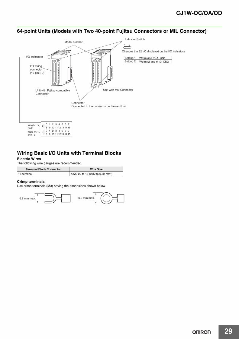
29
CJ1W-OC/OA/OD
64-point Units (Models with Two 40-point Fujitsu Connectors or MIL Connector)
Wiring Basic I/O Units with Terminal BlocksElectric WiresThe following wire gauges are recommended.
Crimp terminalsUse crimp terminals (M3) having the dimensions shown below.
Terminal Block Connector Wire Size
18-terminal AWG 22 to 18 (0.32 to 0.82 mm2)
ID261
0 1 2 3 4 5 6 78 9 12 13 14 1510 110 1 2 3 4 5 6 78 9 12 13 14 1510 11
I
II
ID261
1 2Model number
I/O indicators
Unit with MIL ConnectorUnit with Fujitsu-compatibleConnector
ConnectorConnected to the connector on the next Unit.
Indicator Switch
Changes the 32 I/O displayed on the I/O indicators.
Setting 1Setting 2
I/O wiringconnector(40-pin × 2)
Wd m and m+1: CN1Wd m+2 and m+3: CN2
Word m orm+2
Word m+1or m+3
6.2 mm max. 6.2 mm max.

CJ1W-OC/OA/OD
30
I/O Unit Wiring MethodsAn I/O Unit can be connected to an external device by any of the following three methods.
1. User-provided CableAn I/O Unit can be directly connected to an external device by using a connector.
2. Connector-Terminal Block Conversion UnitUse a Connecting Cable to connect to a Connector-Terminal Block Conversion Unit. Converting the I/O Unit connector to a screw terminal block makes it easy to connect external devices.
3. I/O Relay TerminalUse a Connecting Cable to connect to an I/O Relay Terminal. The I/O specifications can be converted to relay outputs and AC inputs by connecting the I/O Relay Terminal to an I/O Unit.
B
C
A
A User-provided cable
B External device
C Connector
B
C
A
A Connecting Cable for Connector-Terminal Block Conversion UnitXW2Z
B Connector-Terminal Block Conversion UnitXW2R
C Conversion to a screw terminal block
B
B
A
A G79 I/O Relay Terminal Connecting Cable
B G7@@ I/O Relay TerminalsOr, conversion to relay outputs and AC inputs.

31
CJ1W-OC/OA/OD
1. Using User-made Cables with ConnectorAvailable ConnectorsUse the following connectors when assembling a connector and cable.
32- and 64-point Basic I/O Units with Fujitsu-compatible ConnectorsApplicable Units
Applicable Cable-side Connectors
32- and 64-point Basic I/O Units with MIL ConnectorsApplicable Units
Applicable Cable-side Connectors
*1. Socket and Stain Relief set.*2. Crimp Contacts (XG5W-0232) are sold separately.*3. Applicable wire size is AWG 28 to 24. For applicable conductor construction and more information, visit the OMRON website at
www.ia.omron.com.
Wire SizeWe recommend using cable with wire gauges of AWG 28 to 24 (0.08 to 0.2 mm2). Use cable with external wire diameters of 1.61 mm max.
Crimping ToolsThe following models are recommended for crimping tools and pressure-welding tools for Fujitsu connectors. Tools for Crimped Connectors (Fujitsu Component)
Tools for Pressure-welded Connectors (Fujitsu Component)
The following models are recommended for tools for OMRON MIL connectors.Tools for Pressure-welded Connectors (OMRON)
Tools for Crimped Connectors (OMRON)
Model Specifications Pins
CJ1W-OD231 Transistor Output Unit with Sinking Outputs, 32 outputs 40
CJ1W-OD261 Transistor Output Unit with Sinking Outputs, 64 outputs
Connection Pins OMRON set Fujitsu parts
Solder-type 40 C500-CE404Socket: FCN-361J040-AUConnector cover: FCN-360C040-J2
Crimped 40 C500-CE405Socket: FCN-363J040Connector cover: FCN-360C040-J2Contacts: FCN-363J-AU
Pressure-welded 40 C500-CE403 FCN-367J040-AU/F
Model Specifications Pins
CJ1W-OD232 Transistor Output Unit with sourcing outputs, 32 outputs
40CJ1W-OD262 Transistor Output Unit with sourcing outputs, 64 outputs
CJ1W-OD233CJ1W-OD234 Transistor Output Unit with sinking outputs, 32 outputs
CJ1W-OD263 Transistor Output Unit with sinking outputs, 64 outputs
Connection Pins OMRON set DDK parts
Pressure-welded 40 XG4M-4030-T *1 FRC5-A040-3T0S
Crimped
40 XG5N-401 *2 HU-40OS2-001
−Crimp Contacts for XG5N *3XG5W-0232 (loose contacts: 100 pieces)XG5W-0232-R (reel contacts: 10,000 pieces)
HU-111S
Product Name Model
Hand Crimping Tool FCN-363T-T005/H
Contact Withdrawal Tool FCN-360T-T001/H
Product Name Model
Hand Press FCN-707T-T101/H
Cable Cutter FCN-707T-T001/H
Locator Plate FCN-367T-T012/H
Product Name Model
Pressure-welding Tool XY2B-0002
Attachment XY2B-1007
Product Name Model
Manual Crimping Tool XY2B-7007

CJ1W-OC/OA/OD
32
2. Connecting Connector-Terminal Block Conversion UnitsConnection Patterns for Connector-Terminal Block Conversion Units
Combination of I/O Units with Connector-Terminal Block Conversion Units
Pattern Configuration Number of Connectors
A 1
B 2
Unit I/O capacity
Number ofconnectors Polarity Connection
patternConnecting
Cable
Connector-Terminal Block
Conversion UnitWiring method Common
terminals
CJ1W-OD231 32 outputs 1 Fujitsu
connector NPN A XW2Z-@@@B
XW2R-J34G-C3 Phillips screw
NoXW2R-E34G-C3 Slotted screw (rise up)
XW2R-P34G-C3 Push-in spring
CJ1W-OD232 32 outputs 1 MIL
connector PNP A XW2Z-@@@K
XW2R-J34G-C4 Phillips screw
NoXW2R-E34G-C4 Slotted screw (rise up)
XW2R-P34G-C4 Push-in spring
CJ1W-OD233 32 outputs 1 MIL
connector NPN A XW2Z-@@@K
XW2R-J34G-C4 Phillips screw
NoXW2R-E34G-C4 Slotted screw (rise up)
XW2R-P34G-C4 Push-in spring
CJ1W-OD234 32 outputs 1 MIL
connector NPN A XW2Z-@@@K
XW2R-J34G-C4 Phillips screw
NoXW2R-E34G-C4 Slotted screw (rise up)
XW2R-P34G-C4 Push-in spring
CJ1W-OD261 64 outputs 2 Fujitsu
connectors NPN B XW2Z-@@@B (2 Cables)
XW2R-J34G-C3 (2 Units) Phillips screw
NoXW2R-E34G-C3 (2 Units) Slotted screw (rise up)
XW2R-P34G-C3 (2 Units) Push-in spring
CJ1W-OD262 64 outputs 2 MIL
connectors PNP B XW2Z-@@@K (2 Cables)
XW2R-J34G-C4 (2 Units) Phillips screw
NoXW2R-E34G-C4 (2 Units) Slotted screw (rise up)
XW2R-P34G-C4 (2 Units) Push-in spring
CJ1W-OD263 64 outputs 2 MIL
connectors NPN B XW2Z-@@@K (2 Cables)
XW2R-J34G-C4 (2 Units) Phillips screw
NoXW2R-E34G-C4 (2 Units) Slotted screw (rise up)
XW2R-P34G-C4 (2 Units) Push-in spring
Connecting Cable
34 terminals
Connector-Terminal Block Conversion Unit
Connecting Cable
34 terminals 34 terminals
Connector-Terminal Block Conversion Unit

33
CJ1W-OC/OA/OD
Types of Connecting Cables
3. Connecting I/O Relay TerminalsConnection Patterns for I/O Relay Terminals
Combination of I/O Units with I/O Relay Terminal and Connecting Cables
Appearance Connectors Model Cable lenght [m]
XW2Z-@@@B
One 40-pin Connector Made by Fujitsu Component, Ltd. to One 40-pin MIL Connector
XW2Z-050B 0.5
XW2Z-100B 1
XW2Z-150B 1.5
XW2Z-200B 2
XW2Z-300B 3
XW2Z-500B 5
XW2Z-@@@K
One 40-pin MIL Connector to One 40-pin MIL Connector
XW2Z-C50K 0.5
XW2Z-100K 1
XW2Z-150K 1.5
XW2Z-200K 2
XW2Z-300K 3
XW2Z-500K 5
Pattern Configuration
A
B
Unit I/O capacity Number of connectors Polarity Connection
patternNumber of branches Connecting Cable I/O Relay Terminal
CJ1W-OD231 32 outputs 1 Fujitsu connector NPN
A 2 G79-O@C-@ G7TC-OC16
A 2 G79-O@C-@ G7TC-OC08
A 2 G79-O@C-@ G70D-SOC16
A 2 G79-O@C-@ G70D-FOM16
A 2 G79-O@C-@ G70D-VSOC16
A 2 G79-O@C-@ G70D-VFOM16
A 2 G79-O@C-@ G70A-ZOC16-3 and Relay
A 2 G79-O@C-@ G70R-SOC08
A 2 G79-O@C-@ G70D-SOC08
CJ1W-OD232 32 outputs 1 MIL connector PNP
A 2 G79-I@-@-D1 G7TC-OC16-1
A 2 G79-O@-@-D1 G70D-SOC16-1
A 2 G79-O@-@-D1 G70D-FOM16-1
A 2 G79-O@-@-D1 G70A-ZOC16-4 and Relay
Connecting Cable
I/O Relay Terminal
Connecting Cable
I/O Relay Terminal I/O Relay Terminal

CJ1W-OC/OA/OD
34
Types of Connecting Cables
CJ1W-OD233 32 outputs 1 MIL connector NPN
A 2 G79-O@-@-D1 G7TC-OC16
A 2 G79-O@-@-D1 G7TC-OC08
A 2 G79-O@-@-D1 G70D-SOC16
A 2 G79-O@-@-D1 G70D-FOM16
A 2 G79-O@-@-D1 G70D-VSOC16
A 2 G79-O@-@-D1 G70D-VFOM16
A 2 G79-O@-@-D1 G70A-ZOC16-3 and Relay
A 2 G79-O@-@-D1 G70R-SOC08
A 2 G79-O@-@-D1 G70D-SOC08
CJ1W-OD234 32 outputs 1 MIL connector NPN
A 2 G79-O@-@-D1 G7TC-OC16
A 2 G79-O@-@-D1 G7TC-OC08
A 2 G79-O@-@-D1 G70D-SOC16
A 2 G79-O@-@-D1 G70D-FOM16
A 2 G79-O@-@-D1 G70D-VSOC16
A 2 G79-O@-@-D1 G70D-VFOM16
A 2 G79-O@-@-D1 G70A-ZOC16-3 and Relay
A 2 G79-O@-@-D1 G70R-SOC08
A 2 G79-O@-@-D1 G70D-SOC08
CJ1W-OD261 64 outputs 2 Fujitsu connectors NPN
B 2 G79-O@C-@ G7TC-OC16
B 2 G79-O@C-@ G7TC-OC08
B 2 G79-O@C-@ G70D-SOC16
B 2 G79-O@C-@ G70D-FOM16
B 2 G79-O@C-@ G70D-VSOC16
B 2 G79-O@C-@ G70D-VFOM16
B 2 G79-O@C-@ G70A-ZOC16-3 and Relay
B 2 G79-O@C-@ G70R-SOC08
B 2 G79-O@C-@ G70D-SOC08
CJ1W-OD262 64 outputs 2 MIL connectors PNP
B 2 G79-I@-@-D1 G7TC-OC16-1
B 2 G79-O@-@-D1 G70D-SOC16-1
B 2 G79-O@-@-D1 G70D-FOM16-1
B 2 G79-O@-@-D1 G70A-ZOC16-4 and Relay
CJ1W-OD263 64 outputs 2 MIL connectors NPN
B 2 G79-O@-@-D1 G7TC-OC16
B 2 G79-O@-@-D1 G7TC-OC08
B 2 G79-O@-@-D1 G70D-SOC16
B 2 G79-O@-@-D1 G70D-FOM16
B 2 G79-O@-@-D1 G70D-VSOC16
B 2 G79-O@-@-D1 G70D-VFOM16
B 2 G79-O@-@-D1 G70A-ZOC16-3 and Relay
B 2 G79-O@-@-D1 G70R-SOC08
B 2 G79-O@-@-D1 G70D-SOC08
Cable length G79-O@C-@ G79-O@-@-D1 G79-I@-@-D1
0.25m − − −
0.5m − G79-O50-25-D1 G79-I50-25-D1
1.0m G79-O100C-75 G79-O75-50-D1 G79-I75-50-D1
1.5m G79-O150C-125 − −
2.0m G79-O200C-175 − −
3.0m G79-O300C-275 − −
5.0m G79-O500C-475 − −
Unit I/O capacity Number of connectors Polarity Connection
patternNumber of branches Connecting Cable I/O Relay Terminal

35
CJ1W-OC/OA/OD
Dimensions (Unit: mm)
8-point/16-point Units (18-point Terminal Blocks)CJ1W-OC201/ OC211/ OA201/ OD201 / OD202/ OD203/ OD204/ OD211/ OD213 / OD212
32-point Unit (Output Units)With Fujitsu-Compatible Connector (40-pin × 1)CJ1W-OD231
With MIL Connector (40-pin × 1)CJ1W-OD232 / OD233 / OD234
ID2110 1 2 3 4 5 6 7
8 9 10 11 12 13 14 15
01
32
45
76
89
1110
1213
1415
DC24V7mA
COMCOM
2.7
2.7
90
6589
31
ID2310
0
1
20
A B
20
1
1
1 2 34 5 6 78 9 10 1112 13 14 15
DC
24V
4.1
mA
2.7
2.7
90
6566.5
(112.5)
20
ID2310
0 1
1ch
0ch
1 2 34 5 6 78 9 10 1112 13 14 15
DC
24V
4.1
mA
6583.6
2.7
2.7
90
20

CJ1W-OC/OA/OD
36
64-point Units (Output Units)With Fujitsu-Compatible Connector (40-pin × 2)CJ1W-OD261
With MIL Connector (40-pin × 2)CJ1W-OD262 / OD263
Related Manuals
Name Cat. No. Contents
CJ-series CJ2 CPU Unit Hardware User's ManualCJ2H-CPU6@-EIPCJ2H-CPU6@CJ2M-CPU@@
W472
Describes the following for CJ2 CPU Units:• Overview and features• Basic system configuration• Part nomenclature and functions• Mounting and setting procedure• Remedies for errors• Also refer to the Software User’s Manual (W473).
CJ Series CJ1H-CPU@@H-R, CJ1G/H-CPU@@H, CJ1G-CPU@@P, CJ1G-CPU@@, CJ1M-CPU@@ Programmable Controllers Operation Manual
W393 Provides an outlines of and describes the design, installation, maintenance, and other basic operations for the CJ-series PLCs.
NJ-series CPU Unit Hardware User's Manual NJ501-@@@@
W500
An introduction to the entire NJ-series system is provided along with the following information on a Controller built with an NJ501 CPU Unit.• Features and system configuration• Introduction• Part names and functions• General specifications• Installation and wiring• Maintenance and inspection
Use this manual together with the NJ-series CPU Unit Software User's Manual (Cat. No. W501).
65
66.5
(112.5)
31
902.
72.
7
83.6
65
902.
72.
7
31

Terms and Conditions Agreement Read and understand this catalog. Please read and understand this catalog before purchasing the products. Please consult your OMRON representative if you have any questions or comments. Warranties. (a) Exclusive Warranty. Omron’s exclusive warranty is that the Products will be free from defects in materials and workmanship for a period of twelve months from the date of sale by Omron (or such other period expressed in writing by Omron). Omron disclaims all other warranties, express or implied. (b) Limitations. OMRON MAKES NO WARRANTY OR REPRESENTATION, EXPRESS OR IMPLIED, ABOUT NON-INFRINGEMENT, MERCHANTABILITY OR FITNESS FOR A PARTICULAR PURPOSE OF THE PRODUCTS. BUYER ACKNOWLEDGES THAT IT ALONE HAS DETERMINED THAT THE PRODUCTS WILL SUITABLY MEET THE REQUIREMENTS OF THEIR INTENDED USE. Omron further disclaims all warranties and responsibility of any type for claims or expenses based on infringement by the Products or otherwise of any intellectual property right. (c) Buyer Remedy. Omron’s sole obligation hereunder shall be, at Omron’s election, to (i) replace (in the form originally shipped with Buyer responsible for labor charges for removal or replacement thereof) the non-complying Product, (ii) repair the non-complying Product, or (iii) repay or credit Buyer an amount equal to the purchase price of the non-complying Product; provided that in no event shall Omron be responsible for warranty, repair, indemnity or any other claims or expenses regarding the Products unless Omron’s analysis confirms that the Products were properly handled, stored, installed and maintained and not subject to contamination, abuse, misuse or inappropriate modification. Return of any Products by Buyer must be approved in writing by Omron before shipment. Omron Companies shall not be liable for the suitability or unsuitability or the results from the use of Products in combination with any electrical or electronic components, circuits, system assemblies or any other materials or substances or environments. Any advice, recommendations or information given orally or in writing, are not to be construed as an amendment or addition to the above warranty. See http://www.omron.com/global/ or contact your Omron representative for published information. Limitation on Liability; Etc. OMRON COMPANIES SHALL NOT BE LIABLE FOR SPECIAL, INDIRECT, INCIDENTAL, OR CONSEQUENTIAL DAMAGES, LOSS OF PROFITS OR PRODUCTION OR COMMERCIAL LOSS IN ANY WAY CONNECTED WITH THE PRODUCTS, WHETHER SUCH CLAIM IS BASED IN CONTRACT, WARRANTY, NEGLIGENCE OR STRICT LIABILITY. Further, in no event shall liability of Omron Companies exceed the individual price of the Product on which liability is asserted. Suitability of Use. Omron Companies shall not be responsible for conformity with any standards, codes or regulations which apply to the combination of the Product in the Buyer’s application or use of the Product. At Buyer’s request, Omron will provide applicable third party certification documents identifying ratings and limitations of use which apply to the Product. This information by itself is not sufficient for a complete determination of the suitability of the Product in combination with the end product, machine, system, or other application or use. Buyer shall be solely responsible for determining appropriateness of the particular Product with respect to Buyer’s application, product or system. Buyer shall take application responsibility in all cases. NEVER USE THE PRODUCT FOR AN APPLICATION INVOLVING SERIOUS RISK TO LIFE OR PROPERTY OR IN LARGE QUANTITIES WITHOUT ENSURING THAT THE SYSTEM AS A WHOLE HAS BEEN DESIGNED TO ADDRESS THE RISKS, AND THAT THE OMRON PRODUCT(S) IS PROPERLY RATED AND INSTALLED FOR THE INTENDED USE WITHIN THE OVERALL EQUIPMENT OR SYSTEM. Programmable Products. Omron Companies shall not be responsible for the user’s programming of a programmable Product, or any consequence thereof. Performance Data. Data presented in Omron Company websites, catalogs and other materials is provided as a guide for the user in determining suitability and does not constitute a warranty. It may represent the result of Omron’s test conditions, and the user must correlate it to actual application requirements. Actual performance is subject to the Omron’s Warranty and Limitations of Liability. Change in Specifications. Product specifications and accessories may be changed at any time based on improvements and other reasons. It is our practice to change part numbers when published ratings or features are changed, or when significant construction changes are made. However, some specifications of the Product may be changed without any notice. When in doubt, special part numbers may be assigned to fix or establish key specifications for your application. Please consult with your Omron’s representative at any time to confirm actual specifications of purchased Product. Errors and Omissions. Information presented by Omron Companies has been checked and is believed to be accurate; however, no responsibility is assumed for clerical, typographical or proofreading errors or omissions.
2014.4
In the interest of product improvement, specifications are subject to change without notice.
OMRON Corporation Industrial Automation Company http://www.ia.omron.com/
(c)Copyright OMRON Corporation 2014 All Right Reserved.

The
info
rmat
ion
prov
ided
in th
is d
ocum
enta
tion
cont
ains
gen
eral
des
crip
tions
and
/or t
echn
ical
cha
ract
eris
tics
of th
e pe
rform
ance
of t
he p
rodu
cts
cont
aine
d he
rein
.Th
is d
ocum
enta
tion
is n
ot in
tend
ed a
s a
subs
titut
e fo
r and
is n
ot to
be
used
for d
eter
min
ing
suita
bilit
y or
relia
bilit
y of
thes
e pr
oduc
ts fo
r spe
cific
use
r app
licat
ions
.It
is th
e du
ty o
f any
suc
h us
er o
r int
egra
tor t
o pe
rform
the
appr
opria
te a
nd c
ompl
ete
risk
anal
ysis
, eva
luat
ion
and
test
ing
of th
e pr
oduc
ts w
ith re
spec
t to
the
rele
vant
spe
cific
app
licat
ion
or u
se th
ereo
f.N
eith
er S
chne
ider
Ele
ctric
Indu
strie
s SA
S no
r any
of i
ts a
ffilia
tes
or s
ubsi
diar
ies
shal
l be
resp
onsi
ble
or li
able
for m
isus
e of
the
info
rmat
ion
cont
aine
d he
rein
.
Oct 31, 20121
Product data sheetCharacteristics
TM238LFDC24DTcompact base M238 - 24 I/O - 24 V DC supply -CANOpen - internal RAM 1000 kB
MainCommercial Status CommercialisedRange of product Modicon M238 logic controllerProduct or componenttype
Compact base
Product specific appli-cation
-
Discrete I/O number 24Discrete input number 8 fast input conforming to EN/IEC 61131-2 type 1
6 input conforming to EN/IEC 61131-2 type 1Discrete input voltage 24 VDiscrete input voltagetype
DC
Discrete output number 6 output4 fast output
Discrete output voltage 24 V DCNumber of I/O expan-sion module
7
[Us] rated supply volt-age
24 V DC
Memory description Internal RAM 1000 kBData backed up Variables of type retain and retain persistent option-
al battery lithium thionyl chloride (TSXPLP01) 1 yearVariables of type retain and retain persistent internalbattery 3 days 22 h 10 yr
Mounting support 35 mm symmetrical DIN railPanel
ComplementaryDiscrete input logic Sink or source (positive/negative) input
Positive logic (sink) fast inputNumber of common point 4 fast input
2 output1 input1 fast output
Sensor power supply 19.2...30 V DCVoltage state1 guaranteed >= 15 V input/fast inputCurrent state 1 guaranteed >= 2 mA input/fast inputVoltage state 0 guaranteed <= 5 V input/fast inputCurrent state 0 guaranteed <= 1.5 mA input/fast inputDiscrete input current 8 mA fast input
10.4 mA inputInput impedance 3 kOhm fast input
2.3 kOhm inputResponse time 300 ns fast input
3 ms input0.25 ms fast output< 1 ms output
Configurable filtering time 4 ms fast input2 ms fast input1 ms fast input0.4 ms fast input0.004 ms fast input

2
Anti bounce filtering 4 ms configurable input/fast input12 ms configurable input/fast input1.5 ms configurable input/fast input0 ms configurable input/fast input
Input frequency <= 100 kHz input<= 100 kHz fast input (normal mode)<= 100 kHz fast input (counter mode)
Cable length <= 30 m shielded cable fast output (normal mode)<= 30 m output<= 30 m input<= 30 m fast input (normal mode)<= 10 m shielded cable fast input (counter mode)<= 10 m fast output (PWM or PTO mode)
Isolation between channels and internal logic 500 V DCIsolation between channels None input
500 V for output and fast output500 V for group of 2 fast inputs
Discrete output logic Positive logic (source)/negative logic (sink)Output voltage limits 19.2...30 VDiscrete output current 20...500 mA output
<= 500 mA fast output (normal mode)<= 100 mA fast output (PWM mode)<= 100 mA fast output (PTO mode)
Output frequency <= 20 kHz fast output (PWM mode)<= 100 kHz output<= 100 kHz fast output (PTO mode)
Absolute accuracy error 1 % of full scale fast output (PTO mode)1 % of full scale cyclic ratio 20...80% fast output (PWM mode)
Leakage current 0.05 mA output<= 2 mA fast output
[Ures] residual voltage <= 2 V output and fast outputTungsten load <= 3 W output and fast outputShort-circuit protection With output and fast outputOvervoltage protection With output and fast outputOverload protection With output and fast outputInput/Output number <= 248 HE-10 connector with I/O expansion module
<= 192 spring terminal block with I/O expansion module<= 136 removable screw terminal block with I/O expansion module
Supply voltage limits 19.2...28.8 VInrush current <= 35 APower consumption in W <= 17.2 WInsulation resistance > 10 MOhm at 500 V, between supply and earth terminals
> 10 MOhm at 500 V, between I/O and earth terminalsExact time for 1 Kinstruction 0.3 ms 70 % Boolean + 30 % fixed arithmeticExecution time per instruction 7.25 µs arithmetic REAL floating by operation
5111 µs arithmetic REAL floating +, -, x operations0.971 µs Boolean0.648 µs arithmetic REAL floating LD and ST0.506 µs arithmetic DINT double-word +, -, x operations0.459 µs arithmetic DINT double-word LD and ST0.439 µs arithmetic INT word +, -, x operations0.42 µs arithmetic INT word LD and ST
Exct time for event task 0.95 ms arithmetic DINT double-word>= 0.75 ms arithmetic INT word<= 1.75 ms arithmetic REAL floating
System overhead 0.9 ms master task (I/O)0.35 ms master task (advanced counting)0.2 ms master task (PTO)0.15 ms master task (simple counting)0.15 ms master task (PWM, frequency meter)
Input output assignment Reading/Writing I/O on extension modulesReading/Writing I/O on CANopen busReading/Writing I/O on base
Application structure 1 configurable freewheeling/cyclic master task2 configurable freewheeling/cyclic/event auxiliary tasks32 levels of priority between tasks4 interrupt tasks
Realtime clock With 10 s/month at 25 °C

3
Integrated connection type CANopen removable screw terminal block CANopen1 isolated serial link female RJ45 Modbus master/slave RTU/ASCII, charactermode or SoMachine-Network RS232/RS485 1.2...38.4 kbit/s (19.2 kbit/s by de-fault)1 isolated serial link female RJ45 Modbus master/slave RTU/ASCII or SoMa-chine-Network RS485 1.2...115.2 kbit/s (115.2 kbit/s by default)
Supply Serial link supply 5 V 200 mACANopen feature profile DR 303-1
DS 301 V4.02Transmission rate 800 kbit/s 50 m CANopen
500 kbit/s 100 m CANopen50 kbit/s 1000 m CANopen425 kbit/s 125 m CANopen250 kbit/s 250 m CANopen125 kbit/s 500 m CANopen1000 kbit/s 20 m CANopen
Positioning functions PWM/PTO 2 100 kHzCounting input number 8 100 kHz 32 bitsComplementary function Event processing
PIDMarking CELocal signalling 1 LED SL2
1 LED SL11 LED PWR1 LED per channel I/O state1 LED module error (ERR)1 LED CAN RUN1 LED CAN ERR1 LED Batt1 LED RUN
Electrical connection 1 removable screw terminal block for connecting the 24 V DC power supply1 removable screw terminal block (7 terminals) for connecting the sensors (in-puts)1 removable screw terminal block (6 terminals) for connecting the 6 preactuators(output)1 removable screw terminal block (5 terminals) for connection to the CANopenbus1 removable screw terminal block (12 terminals) for connecting the sensors (fastinputs)1 removable screw terminal block (10 terminals) for connecting the 4 preactua-tors (fast output)1 connector mini B USB 2.0 for a programming terminal
Product weight 0.595 kg
EnvironmentImmunity to microbreaks 10 msDielectric strength 500 V for 1 minute, between supply and earth terminals
500 V for 1 minute, between I/O and earth terminalsClass Class M20 <= 16 CANopenProduct certifications CSA
CTickGOSTUL
Ambient air temperature for operation -10...55 °CAmbient air temperature for storage -40...70 °CRelative humidity 95 % without condensationIP degree of protection IP20Pollution degree <= 2Operating altitude 0...2000 mStorage altitude 0...3000 mVibration resistance 1 gn 3.5 mm (f= 5...150 Hz)Shock resistance 15 gn for 11 msHeight 118 mmDepth 86 mmWidth 157 mm

4
Product data sheetDimensions Drawings
TM238LFDC24DT
Modicon M238 Logic Controller
Dimensions

5
Product data sheetMounting and Clearance
TM238LFDC24DT
Clearance
Mounting on a DIN Rail
Dimensions of the DIN Rail
Mounting on a Metallic Panel
Mounting Holes

6
Mounting the Modicon M238 Logic Controller on a Metallic Panel
7
Product data sheetConnections and Schema
TM238LFDC24DT
Wiring Requirements
Rules for Removable Screw Terminal Block
Rules for Removable Spring Terminal Block
DC Power Supply
Wiring Diagram
Use an external fast-blow fuse 2 A type F (UL recognized and CSA approved).
Regular Inputs
Wiring Diagram
(1) Fast-blow fuse 0.5 A(2) Sink input (positive logic)(3) Source input (negative logic)
Fast Inputs

8
Wiring Diagram
(1) Fast-blow fuse 0.5 A
Regular Outputs
Wiring Diagram
(1) Fast-blow fuse 2 A(2) Protection for inductive load
Fast Outputs
Wiring Diagram
(1) 2 A fast-blow fuse(2) Fast-blow fuse: 0.5 A in standard use / 0.1 A in PTO use(3) Protection for inductive load(4) Positive logic output wiring(5) Negative logic output wiring
Example of an incorrect wiring on Q2:
(1) 2 A fast-blow fuse(2) Incorrect wiring
CANopen Connection
Wiring Diagram
R Line termination resistor (120 Ω)

9
Wiring Diagram Examples for 1 Encoder on Fast Inputs
Incremental Encoder with Phase-Shifted Signals with TDC and 3-Wire PNP Detector
(2) Dual-phase encoder with index(4) PNP sensorUse a 0.5 A fast-blow fuse.
Incremental Encoder with Phase-Shifted Signals without TDC and Electromechanical Sensor
(1) Dual-phase encoder without index(3) Limit switchUse a 0.5 A fast-blow fuse.
Wiring Diagram Examples for 2 Encoders on Fast Inputs
Incremental Encoders with Phase-Shifted Signals with TDC
(2) Dual-phase encoder with indexUse a 0.5 A fast-blow fuse.
Incremental Encoders with Phase-Shifted Signals without TDC
(1) Dual-phase encoder without indexUse a 0.5 A fast-blow fuse.