Embed Size (px)
Citation preview

NANO EXPRESS Open Access
Polystyrene negative resist for high-resolutionelectron beam lithographySiqi Ma, Celal Con, Mustafa Yavuz and Bo Cui*
Abstract
We studied the exposure behavior of low molecular weight polystyrene as a negative tone electron beamlithography (EBL) resist, with the goal of finding the ultimate achievable resolution. It demonstrated fairly well-defined patterning of a 20-nm period line array and a 15-nm period dot array, which are the densest patterns everachieved using organic EBL resists. Such dense patterns can be achieved both at 20 and 5 keV beam energiesusing different developers. In addition to its ultra-high resolution capability, polystyrene is a simple and low-costresist with easy process control and practically unlimited shelf life. It is also considerably more resistant to dryetching than PMMA. With a low sensitivity, it would find applications where negative resist is desired andthroughput is not a major concern.
1. IntroductionElectron beam lithography (EBL) [1], focused ion beam(FIB) lithography [2], and nanoimprint lithography (NIL)[3] are currently the three most widely employed nano-lithography techniques. Among them, EBL is undoubt-edly the most popular for R&D. Unlike NIL, EBL cangenerate arbitrary patterns without the need of fabricat-ing a mold first. Though not as versatile as FIB, whichcan do both lithography using a resist and milling, EBL iscapable of exposing thick (> > 100 nm) resist without ioncontamination to the resist. In addition, it is faster thanFIB exposure since the electron beam can remain well-focused below 10-nm beam size even with nA beam cur-rent, as is needed for fast writing. In recent years, onemain trend in EBL development is the effort being madetoward ultra-high resolution and pattern density, withthe record pattern density of 9-nm period line arrays [4].Desirable properties for EBL resist include high sensitiv-ity, high contrast, and high dry etching selectivity to thesubstrate materials. Positive resist is typically used forEBL, largely because of the availability of the benchmarkresist poly(methyl methacrylate) (PMMA) that offershigh resolution with low cost and ease of process. Withits higher sensitivity and etching resistance than PMMA,ZEP520 (positive-tone, Zeon Corp.) is arguably the sec-ond most popular EBL resist.
However, for some applications, such as the fabricationof hole arrays in a metal film (the structure for extraor-dinary optical transmission [5]) by using liftoff, negativeresist would offer substantially shorter exposure time,except when using a more complicated “resist tone rever-sal” process [6]. Unfortunately, there is no negative resistthat gains similar popularity as PMMA and ZEP520.Bilenberg et al. have selected four negative EBL resistsand compared their performance: calixarene (TokuyamaCorp.), ma-N 2401 (Microresist Technology), SU-8(Microchem Corp.), and mr-L 6000 (Microresist Tech-nology) [7]. As chemically amplified resists, SU-8 andmr-L 6000 offer superior sensitivity, but with low con-trast and resolution (more strictly speaking, half-pitch fordense periodic line array patterns), which is limited bythe diffusion of the photoacid generator during postbak-ing. Ma-N 2401 has sensitivity comparable to that ofZEP520 resist, but with far inferior resolution. Amongthe four resists, calixarene offers the highest resolution.Calixarene has been studied as a candidate resist for fab-ricating using EBL bit-patterned recording media thathave achieved areal density of 1.4 and 1.6 Tbits/in2 (cor-responding to a dot array of 20-nm period) [8,9] usingvery thin (sub-20 nm) film. However, it has low sensitiv-ity despite being a chemically amplified resist, and theacid generated in the exposed area may diffuse into theunexposed area, blurring the latent image.In recent years, hydrogen silsesqioaxene (HSQ) prob-
ably attracted more attention than any other negative
* Correspondence: [email protected] Institute for Nanotechnology (WIN), University of Waterloo, 200University Ave. West, Waterloo, ON N2L 3G1, Canada
Ma et al. Nanoscale Research Letters 2011, 6:446http://www.nanoscalereslett.com/content/6/1/446
© 2011 Ma et al; licensee Springer. This is an Open Access article distributed under the terms of the Creative Commons AttributionLicense (http://creativecommons.org/licenses/by/2.0), which permits unrestricted use, distribution, and reproduction in any medium,provided the original work is properly cited.
tone resist [10-12]. HSQ is an excellent inorganic EBLresist that has demonstrated the highest resolution of9-nm period line array patterns [4,13], thanks to itssmall molecular size and lack of swelling during devel-opment [14]. (Metal halides have actually demonstratedbetter resolution, but they are not practical resists dueto their extremely low sensitivity and inability to formarbitrary patterns [1].) However, in addition to its lowsensitivity, HSQ is not suitable for liftoff unless whenused with a double layer resist stack, such as HSQcoated on PMMA. The development process is also self-limiting due to crosslinking of resist by the developer,leading to incomplete removal of unexposed resist,though a salty developer can minimize this effect [4,15].Moreover, HSQ is unstable, and so spin coating, baking,exposure, and development must be done quickly (yet,this is not possible if the exposure time is long) [16].In addition, all the above resists are commercially formu-
lated with typically high cost and short shelf life. Therefore,it is preferable to have a negative resist like PMMA, whichis a simple polymer with low cost and practically unlimitedshelf life, and can be dissolved easily using various solventsto give the preferred film thickness. Polystyrene is such aresist, as it undergoes crosslinking when exposed to deepUV light or an electron beam. Previously, dense periodicpatterns with 40-nm period lines have been demonstratedusing low molecular weight polystyrene resist [17]. In thisarticle, we investigate the ultimate resolution (half-pitch fordense periodic structure) that can be achieved with poly-styrene, and demonstrate the patterning of 20-nm-periodlines and 15-nm-period 2D dot arrays, which are the high-est densities achieved using organic EBL resists (inorganicresists like HSQ and metal halides have achieved higherresolution). Besides ultrahigh resolution, polystyrene ismore (by approximately 3 ×) resistant to dry etching thanPMMA. Its major drawback is its low sensitivity comparedwith PMMA, which would limit its application to smallscale nano-patterning.
2. ExperimentPolystyrene powder with a molecular weight of 2000 g/mol(Mw/Mn = 1.10) was purchased from Alfa Aesa, and dis-solved in chlorobenzene with a concentration of 1.2 w/v%,which gave a film thickness of 30 nm, as measured byatomic force microscope (AFM), after spin-coating at 2000rpm for 40 s. The silicon wafer was cleaned using acetoneand 2-proponol, followed by short exposure to oxygenplasma. After spin coating, the film was baked at 60°C for1 h on a hotplate. Unlike the high molecular weight poly-styrene, the low molecular weight polystyrene film wasfound to be unstable, forming a non-uniform “broken” filmwhen baked at higher temperatures (e.g., 80°C). In addition,its adhesion to the silicon substrate was not as strong asPMMA. Therefore, in order to obtain reproducible
uniform film, we coated a thin layer antireflection coating(ARC, from Brewer Science), which was further thinned to< 15 nm by oxygen reactive ion etching with 20 W powerand 20 mTorr pressure. This crosslinked and insolublethin under-layer would not affect the pattern transfer byliftoff; although due to lateral etch, certain critical dimen-sion loss is expected when transferring the pattern bydirect etch. Other adhesion promoters, such as a self-assembled monolayer or thin/thinned PMMA film, mightalso improve the adhesion of polystyrene to the siliconsubstrate.Exposure was performed using a LEO 1530 field emis-
sion SEM equipped with a Nabity nanometer pattern gen-eration system at acceleration voltages of 20 and 5 kV.The beam currents were about 20 pA at 20 kV and 10 pAat 5 kV. For high-resolution study, the lines were exposedas single-pass lines with beam step size 3 nm, and dots aszero-dimensional dots. After exposure, the samples weredeveloped using various solvent developers for 90 s atroom temperature or 50°C, followed by a 2-propanolrinse. As crosslinked polystyrene is insoluble, in principle,all solvents that can dissolve (un-exposed) polystyrene canbe used as developer. In this study, we have developed thesamples using xylene (o-, m-, p-mixed), chlorobenzene,and cyclohexane.
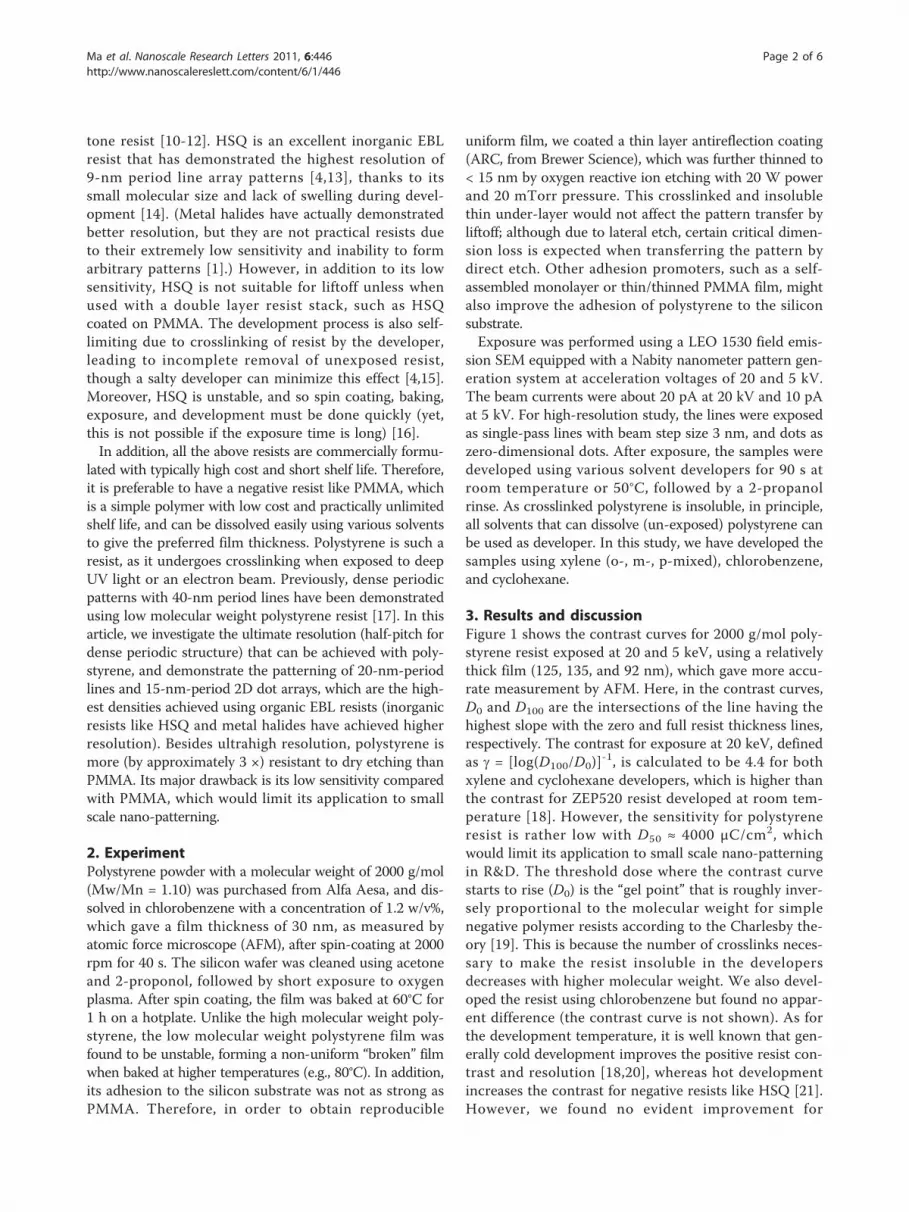
3. Results and discussionFigure 1 shows the contrast curves for 2000 g/mol poly-styrene resist exposed at 20 and 5 keV, using a relativelythick film (125, 135, and 92 nm), which gave more accu-rate measurement by AFM. Here, in the contrast curves,D0 and D100 are the intersections of the line having thehighest slope with the zero and full resist thickness lines,respectively. The contrast for exposure at 20 keV, definedas g = [log(D100/D0)]
-1, is calculated to be 4.4 for bothxylene and cyclohexane developers, which is higher thanthe contrast for ZEP520 resist developed at room tem-perature [18]. However, the sensitivity for polystyreneresist is rather low with D50 ≈ 4000 μC/cm2, whichwould limit its application to small scale nano-patterningin R&D. The threshold dose where the contrast curvestarts to rise (D0) is the “gel point” that is roughly inver-sely proportional to the molecular weight for simplenegative polymer resists according to the Charlesby the-ory [19]. This is because the number of crosslinks neces-sary to make the resist insoluble in the developersdecreases with higher molecular weight. We also devel-oped the resist using chlorobenzene but found no appar-ent difference (the contrast curve is not shown). As forthe development temperature, it is well known that gen-erally cold development improves the positive resist con-trast and resolution [18,20], whereas hot developmentincreases the contrast for negative resists like HSQ [21].However, we found no evident improvement for
Ma et al. Nanoscale Research Letters 2011, 6:446http://www.nanoscalereslett.com/content/6/1/446
Page 2 of 6

Figure 2 Dense line array with a period of (a) 100 nm; (b) 30 nm; (c) 25 nm; and (d) 20 nm. The polystyrene resist was exposed at 5 keVand developed using xylene for 1.5 min at room temperature. The pattern heights measured by AFM are in the range of 25-28 nm that is closeto the original film thickness.
Figure 1 Contrast curves for polystyrene exposed at 20 and 5 keV, and developed by xylene and cyclohexane for 90 s at roomtemperature.
Ma et al. Nanoscale Research Letters 2011, 6:446http://www.nanoscalereslett.com/content/6/1/446
Page 3 of 6

polystyrene (negative) resist development at an elevatedtemperature of 50°C. One way to alleviate the issue oflow resist sensitivity is to carry out exposure at low beamenergy such as 5 keV, and the sensitivity was indeedincreased to D50 = 1170 μC/cm2. This is in fair agree-ment with the fact that sensitivity is roughly inverselyproportional to the beam energy (E) as predicted by theBethe equation for electron energy loss (Eloss) in theresist: Eloss ∞ 1/E log(aE) with a being a constant. Sensi-tivity can be further increased using higher molecularweight polystyrene, but at a cost of reduced resolution.When exposed at 5 keV, the contrast is reduced to 3.4,which is close to the ZEP520 resist developed at roomtemperature [18]. The sensitivity and contrast for 5 keVexposure is expected to be similar for cyclohexane andchlorobenzene developers, as it is for the case of 20 keVexposure. As seen below and pointed out also by Cord etal. [13], the reduced contrast did not seriously affect theresist resolution.To study the ultimate resolution (half-pitch) of this
resist, we exposed dense line arrays and dot arrays using30-nm-thick polystyrene at 20 and 5 keV. Thin resist isgenerally used for high resolution patterning in to reducethe effect of capillary force during resist drying, whichleads to pattern collapse (unless using critical point drying[12]), and the forward scattering of electrons that is moreserious for thicker resist [13]. Note that even thinner resistwas used for most previous high resolution studies onHSQ and calixarene resists. For 30-nm polystyrene, theforward scattering range is estimated to be 5 and 8 nm at20 and 5 keV, respectively [13], which are both very low(yet slightly larger than or comparable to the beam spotsize). Therefore, it is expected that EBL at 5 keV canachieve the same resolution as 20 keV, but with the addi-tional benefit of considerably increased resist sensitivity.Figure 2 shows line array patterns of 100, 30, 25, and 20-nm periods developed by xylene for 90 s at room tempera-ture. Line doses ranging from 4 to 10 nC/cm all resultedin well-defined patterns. The dose window is expected tobe much narrower when exposing large area (> 1 μm ×1 μm) line array due to significant exposure from back-scattered electrons. The next period in the experiment,15 nm, was not well defined. The effort toward dense linearray patterning by EBL has been driven by the fabricationof X-ray zone plates where the X-ray imaging resolution isclose to the half-pitch of the outmost zones. Previously,the densest line array pattern demonstrated using organicresist was 24-nm period using ZEP resist developed at lowtemperatures [20] (as mentioned above, the record forinorganic HSQ resist is 9-nm period). As expected andshown in Figure 3, for exposure at 20 keV, a similar highresolution of 20-nm period could be achieved when usingall the three developers (xylene, chlorobenzene, and cyclo-hexane) that are studied.
For dot array patterns, the densest array for whichthe dot is still fairly well defined is with a 15-nm per-iod (Figure 4), which is believed to be the highest pat-tern density ever obtained using organic EBL resists.Here, the array was exposed at 5 keV and developedby xylene and chlorobenzene for 90 s at room tem-perature. The effort toward dense 2D array pattern hasbeen driven by the fabrication of bit-patterned media[22], and the previously evaluated array periods of 18nm (corresponding to 2.0 Tbits/in2) using organic ZEPresist, and 12 nm using inorganic HSQ resist havebeen achieved [23].
Figure 3 Dense line arrays with a period of 20 nm exposed at20 keV and developed at room temperature for 90 s using (a)xylene; (b) chlorobenzene; and (c) cyclohexane. The lines in (c)collapsed due to capillary force during resist drying.
Ma et al. Nanoscale Research Letters 2011, 6:446http://www.nanoscalereslett.com/content/6/1/446
Page 4 of 6

4. ConclusionsWe studied the exposure behavior of the negative EBLresist polystyrene. It demonstrated fairly well-definedpatterns of 20-nm-period line arrays and 15-nm-perioddot arrays, which are the densest patterns ever achievedusing organic EBL resists. Such dense patterns can beachieved both at 20 and 5 keV beam energies, using allthe three developers that were studied. The contrast forpolystyrene is comparable to that of other popularresists like ZEP and PMMA, but its sensitivity is low. Inaddition to its high-resolution capability, polystyrene is asimple and low-cost resist with easy process control andpractically unlimited shelf life. It is also considerablymore resistant to dry etching than PMMA. It wouldfind applications where negative resist is prefered andexposure time is not a major concern.
AbbreviationsAFM: atomic force microscope; ARC: antireflection coating; EBL: electronbeam lithography; FIB: focused ion beam; HSQ: hydrogen silsesqioaxene; NIL:nanoimprint lithography; PMMA: poly(methyl methacrylate).
Authors’ contributionsSM and CC carried out the experiment. BC and MY designed the study. BCanalyzed the data and prepared the manuscript.
Competing interestsThe authors declare that they have no competing interests.
Received: 12 March 2011 Accepted: 12 July 2011Published: 12 July 2011
References1. Grigorescu AE, Hagen CW: Resists for sub-20-nm electron beam
lithography with a focus on HSQ: state of the art. Nanotechnology 2009,20:292001.
2. Tseng AA: Recent developments in micromilling using focused ion beamtechnology. J Micromech Microeng 2004, 14(4):R15-R35.
3. Schift H: Nanoimprint lithography: an old story in modern times? Areview. J Vac Sci Technol B 2008, 26(2):458-480.
4. Yang JKW, Cord B, Duan H, Berggren KK, Klingfus J, Nam SW, Kim KB,Rooks MJ: Understanding of hydrogen silsesquioxane electron resist forsub-5-nm-half-pitch lithography. J Vac Sci Technol B 2009, 27(6):2622-2627.
5. Ebbesen TW, Lezec HJ, Ghaemi HF, Thio T, Wolff PA: Extraordinary opticaltransmission through sub-wavelength hole arrays. Nature 1998,391:667-669.
6. Hajiaboli A, Cui B, Kahrizi M, Truong VV: Optical properties of thick metalnanohole arrays fabricated by electron beam and nanospherelithography. Phys Status Solidi A: Appl Mater Sci 2009, 206(5):976-979.
7. Bilenberg B, Schøler M, Shi P, Schmidt MS, Bøggild P, Fink M, Schuster C,Reuther F, Gruetzner C, Kristensen A: Comparison of high resolutionnegative electron beam resists. J Vac Sci Technol B 2006, 24(4):1776-1779.
8. Hosaka S, Sano H, Itoh K, Sone H: Possibility to form an ultrahigh packedfine pit and dot arrays for future storage using EB writing. MicroelectronEng 2006, 83:792-795.
9. Mohamad ZB, Shirai M, Sone H, Hosaka S, Kodera M: Formation of dotarrays with a pitch of 20 nm × 20 nm for patterned media using 30 keVEB drawing on thin calixarene resist. Nanotechnology 2008, 19:025301.
10. Word MJ, Adesida I, Berger PR: Nanometer-period gratings in hydrogensilsesquioxane fabricated by electron beam lithography. J Vac Sci TechnolB 2003, 21(6):L12-L15.
11. Choi S, Yan MJ, Wang L, Adesida I: Ultra-dense hydrogen silsesquioxane(HSQ) structures on thin silicon nitride membranes. Microelectron Eng2009, 86:521-523.
12. Vila-Comamala J, Gorelick S, Guzenko VA, Farm E, Ritala M, David C: Densehigh aspect ratio hydrogen silsesquioxane nanostructures by 100 keVelectron beam lithography. Nanotechnology 2010, 21:285305.
13. Cord B, Yang J, Duan H, Joy D, Klingfus J, Berggren KK: Limiting factors insub-10 nm scanning-electron-beam lithography. J Vac Sci Technol B 2009,27(6):2616-2621.
14. Sidorkin V, van Run A, van Langen-Suurling A, Grigorescu A, van der Drift E:Towards 2-10 nm electron-beam lithography: a quantitative approach.Microelectron Eng 2008, 85:805-809.
15. Yang JKW, Berggren KK: Using high-contrast salty development ofhydrogen silsesquioxane for sub-10-nm half-pitch lithography. J Vac SciTechnol B 2007, 25(6):2025-2029.
16. Clark N, Vanderslice A, Grove R, Krchnavek RR: Time-dependent exposuredose of hydrogen silsesquioxane when used as a negative electron-beam resist. J Vac Sci Technol B 2006, 24(6):3073-3076.
17. Austin MD, Zhang W, Ge HX, Wasserman D, Lyon SA, Chou SY: 6 nm half-pitch lines and 0.04 μm2 static random access memory patterns bynanoimprint lithography. Nanotechnology 2005, 16:1058-1061.
Figure 4 Dense 2D dot array with a period of 15-nm exposure at 5 keV and developed by chlorobenzene and xylene for 1.5 min atroom temperature.
Ma et al. Nanoscale Research Letters 2011, 6:446http://www.nanoscalereslett.com/content/6/1/446
Page 5 of 6

18. Ocola LE, Stein A: Effect of cold development on improvement inelectron-beam nanopatterning resolution and line roughness. J Vac SciTechnol B 2006, 24(6):3061-3065.
19. Ku HY, Scala LC: Polymeric electron beam resists. J Electrochem Soc 1969,116:980-985.
20. Reinspach J, Lindblom M, von Hofsten O, Bertilson M, Hertz HM,Holmberg A: Cold-developed electron-beam-patterned ZEP 7000 forfabrication of 13 nm nickel zone plates. J Vac Sci Technol B 2009,27(6):2593-2596.
21. Häffner M, Haug A, Heeren A, Fleischer M, Peisert H, Chassé T, Kern DP:Influence of temperature on HSQ electron-beam lithography. J Vac SciTechnol B 2007, 25(6):2045-2048.
22. Yang XM, Xu Y, Lee K, Xiao S, Kuo D, Weller D: Advanced lithography forBit patterned media. IEEE Trans Magn 2009, 45(2):833-838.
23. Yang X, Xiao S, Wu W, Xu Y, Lee K, Kuo D, Weller D: Challenges in 1Teradot/in2 dot patterning using electron beam lithography for bit-patterned media. J Vac Sci Technol B 2007, 25(6):2202-2209.
doi:10.1186/1556-276X-6-446Cite this article as: Ma et al.: Polystyrene negative resist for high-resolution electron beam lithography. Nanoscale Research Letters 20116:446.
Submit your manuscript to a journal and benefi t from:
7 Convenient online submission
7 Rigorous peer review
7 Immediate publication on acceptance
7 Open access: articles freely available online
7 High visibility within the fi eld
7 Retaining the copyright to your article
Submit your next manuscript at 7 springeropen.com
Ma et al. Nanoscale Research Letters 2011, 6:446http://www.nanoscalereslett.com/content/6/1/446
Page 6 of 6


