Embed Size (px)
Citation preview

(19)
Europaisches Patentamt
European Patent Office
Office europeen des brevets
(12)
peen des brevets £ P 0 5 6 9 1 3 4 B 1
EUROPEAN PATENT S P E C I F I C A T I O N
(45) Date of publication and mention of the grant of the patent: 06.08.1997 Bulletin 1997/32
(51) mtci e H03K 1 9 / 1 7 7
(21) Application number: 93302742.7
(22) Date of filing: 07.04.1993
(54) Programmable logic array integrated circuit with cascade connections between logic modules
Integrierte Schaltung einer programmierbaren logischen Anordnung mit kaskadierten Anschlussen zwischen logischen Modulen
Circuit integre a reseau logique programmable avec connexion en cascade entre modules logiques
DO ^ - CO
O) CO lO o a . LU
(84) Designated Contracting States: BE DE DK ES FR GB GR IE IT LU NL PT
(30) Priority: 08.05.1992 US 880888
(43) Date of publication of application: 10.11.1993 Bulletin 1993/45
(73) Proprietor: ALTERA CORPORATION San Jose, California 95134-2020 (US)
(72) Inventors: • Cliff, Richard G.
Milpitas, CA 95035 (US) • Ahanin, Bahram
Cupertino, CA 9501 4 (US)
(74) Representative: Adkins, Michael Withers & Rogers 4 Dyer's Buildings Holborn London EC1N2JT (GB)
(56) References cited: EP-A-0 177 261 US-A-3 473 160
EP-A- 0 415 542
• EDN ELECTRICAL DESIGN NEWS vol. 34, no. 20 , 28 September 1989 , NEWTON, MASSACHUSETTS US pages 91, 93, 94, 96, 98, 100 , XP000067462 D. CONNER 'PLD Architectures Require Scrutiny'
• Architectures Require Scrutiny'
Note: Within nine months from the publication of the mention of the grant of the European patent, any person may give notice to the European Patent Office of opposition to the European patent granted. Notice of opposition shall be filed in a written reasoned statement. It shall not be deemed to have been filed until the opposition fee has been paid. (Art. 99(1) European Patent Convention).
Printed by Jouve, 75001 PARIS (FR)
1 EP 0 569 134 B1 2
Description
Background of the Invention
This invention relates to programmable logic array integrated circuits, and more particularly to a program- mable logic array integrated circuit having improved in- terconnections between the individual logic modules in the circuit.
Commonly assigned, co-pending U.S. patent appli- cation Serial No. 754,01 7, filed September 3, 1 991 (US- A-5 260 610, corresponding to EP-A-0 530 985) shows programmable logic array integrated circuits which are highly modular. In the circuits shown in that application, very similar types of interconnection pathways are used for all types of interconnections between the logic mod- ules. This tends to simplify the design of the circuit. It also tends to simplify the software and/or other tech- niques used to program the circuit to implement partic- ular logic functions. Thus the circuits shown in the above-mentioned application have several important advantages.
There is always room for further improvement, how- ever, and there are some situations in which the provi- sion of additional or alternative types of interconnections between the logic modules would have benefits suffi- cient to justify the additional circuit and programming complexity. Such additional interconnection paths may be desirable for making frequently needed interconnec- tions, for speeding certain kinds of interconnections, for allowing short distance interconnections to be made di- rectly without tying up more general purpose and there- fore long distance interconnection resources, etc. There is also a continuing demand for logic devices with larger capacity. This produces a need to implement logic func- tions more efficiently and to make better use of the por- tion of the device which is devoted to interconnecting individual logic modules.
Wahlstrom U.S. patent 3,473,160 shows cellular logic arrays having programmable logic cells CA1 , CA2, CA3, CB1 , etc., which are interconnectable in a general way by data buses or lines X1B, X1C, Y12, and Y13, and which are also interconnectable in a more limited way by leads such as ZL, Zu, and ZB. Carter U.S. patent 4,642,487 (corresponding to EP-A-0 177 261) shows the same kind of structure. However, in the Carter de- vice the special interconnection circuits merely dupli- cate connections which can be made through the gen- eral interconnect structure. The Carter special intercon- nection circuits may be faster than the general intercon- nect structure, and they may conserve general intercon- nect structure resources, but they do not add any capa- bilities to the circuit. For example, they do not facilitate the performance of more complex logic functions than can be performed by putting the same signals through the general interconnect structure rather than through the special interconnection circuits.
In view of the foregoing, it is an object of this inven-
tion to provide an improved programmable logic array integrated circuit.
It is a more particular object of this invention to pro- vide a programmable logic array integrated circuit with
5 additional possibilities for interconnections between the logic modules which are not mere duplications of inter- connections which can be made through a general pur- pose interconnection network.
10 Summary of the Invention
According to the invention there is provided a pro- grammable logic array integrated circuit comprising a plurality of substantially more than two programmable
is logic modules disposed in a two-dimensional array, each of said logic modules having a plurality of input signal leads, connected to means for producing an out- put signal which is substantially any logical function of the input signals on said input signal leads, and at least
20 one output signal lead; a plurality of first conductors ex- tending along a first dimension of said two-dimensional array; a plurality of second conductors extending along a second dimension of said two-dimensional array; a plurality of switches for making programmable connec-
ts tions between said output signal leads, said first and second conductors, and said input signal leads so that the or each output signal lead of substantially any of said logic modules is connectable to substantially any of said logic module input signal leads, said output signal lead
30 or leads being connectable to at least one of said first and second conductors by said switches, each of said first conductors being connectable to a multiplicity of said second conductors by said switches, and each of said input signal leads being connectable to a multiplie-
rs ity of said conductors by said switches; and a plurality of auxiliary conductors, each of which is associated with a respective one of said logic modules so that a sub- stantial majority of said logic modules have an associ- ated auxiliary conductor, each of said auxiliary conduc-
40 tors connecting the output signal lead of the associated logic module to another receiving logic module which in a substantial majority of cases has an associated aux- iliary conductor connecting its output signal lead to yet another receiving logic module, each of said auxiliary
45 conductors making its connection between the associ- ated logic module and the receiving logic module with- out making use of said first and second conductors or said input signal leads; wherein each of said logic mod- ules in use produces an intermediate signal which is
so said any of a plurality of logical functions of said input signals, characterized in that each of said logic modules includes connect means for selectively modifying the output signal on the output signal lead of said logic mod- ule in accordance with the signal on its associated aux-
55 iliary conductor by logically combining said intermediate output signal of said logic module and the signal re- ceived by said logic module via said auxiliary conductor to produce said output signal of said logic module.
25
30
35
40
45
50
2
3 EP 0 569 134 B1 4
Further features of the invention, its nature and var- ious advantages will be more apparent from the accom- panying drawings and the following detailed description of the preferred embodiments.
Brief Description of the Drawings
FIG. 1 is a simplified schematic block diagram of an illustrative programmable logic array integrated circuit which can include the present invention.
FIG. 2 is a more detailed schematic block diagram of an illustrative embodiment of a representative portion of the circuit of FIG. 1 showing an illustrative embodi- ment of the present invention.
FIG. 3 is a still more detailed schematic block dia- gram of an illustrative embodiment of a representative portion of FIG. 2.
FIG. 4 is a schematic block diagram of a simpler and somewhat more specific embodiment of what is shown in FIG. 3.
FIG. 5 is a schematic block diagram of an illustrative embodiment of a portion of the circuit shown in FIG. 3.
Detailed Description of the Preferred Embodiments
Although this invention can be practiced in the con- text of other types of programmable logic array integrat- ed circuits, the invention will be fully understood from the following explanation of its application to program- mable logic array integrated circuits of the kind shown in commonly assigned, copending U.S. patent applica- tion Serial No. 07/880,942, filed May 8, 1992, corre- sponding to EP-A-0 569 1 37. As shown in FIG. 1 , a pro- grammable logic array integrated circuit 10 has a large number of programmable logic modules 12. Each of log- ic modules 1 2 can perform a relatively simple logic func- tion (e.g., form any logical combination of four inputs). Logic modules 12 are grouped together in groups of eight. Each such group is called a logic array block or LAB 1 4. LABs 1 4 are arranged in a two dimensional ar- ray in circuit 10. This array comprises six rows of 22 LABs per row.
A group of global horizontal conductors 20 is asso- ciated with each row of LABs 14. A group of global ver- tical conductors 22 is associated with each column of LABs 1 4. A signal on any global horizontal conductor 20 can be applied (via local conductors 24) to one or more logic modules 12 in the LAB row associated with that conductor. The output signal of each logic module 12 can be applied to a global horizontal conductor 20 as- sociated with that module's LAB row, and also to one or two global vertical conductors 22 associated with that module's LAB column. The output of each logic module 12 can also be applied to other logic modules in that LAB via local conductors 26 (see FIG. 2, which is again substantially identical to FIG. 2 in the application men- tioned immediately above). Global vertical conductors 22 are connectable to global horizontal conductors 20.
The conductors and connections described in the immediately preceding paragraph comprise the general interconnection circuitry of circuit 10. This general inter- connection circuitry permits any logic module output to
5 be connected to any logic module input so that circuit 1 0 can be programmed to perform large numbers of log- ic functions of almost any desired complexity.
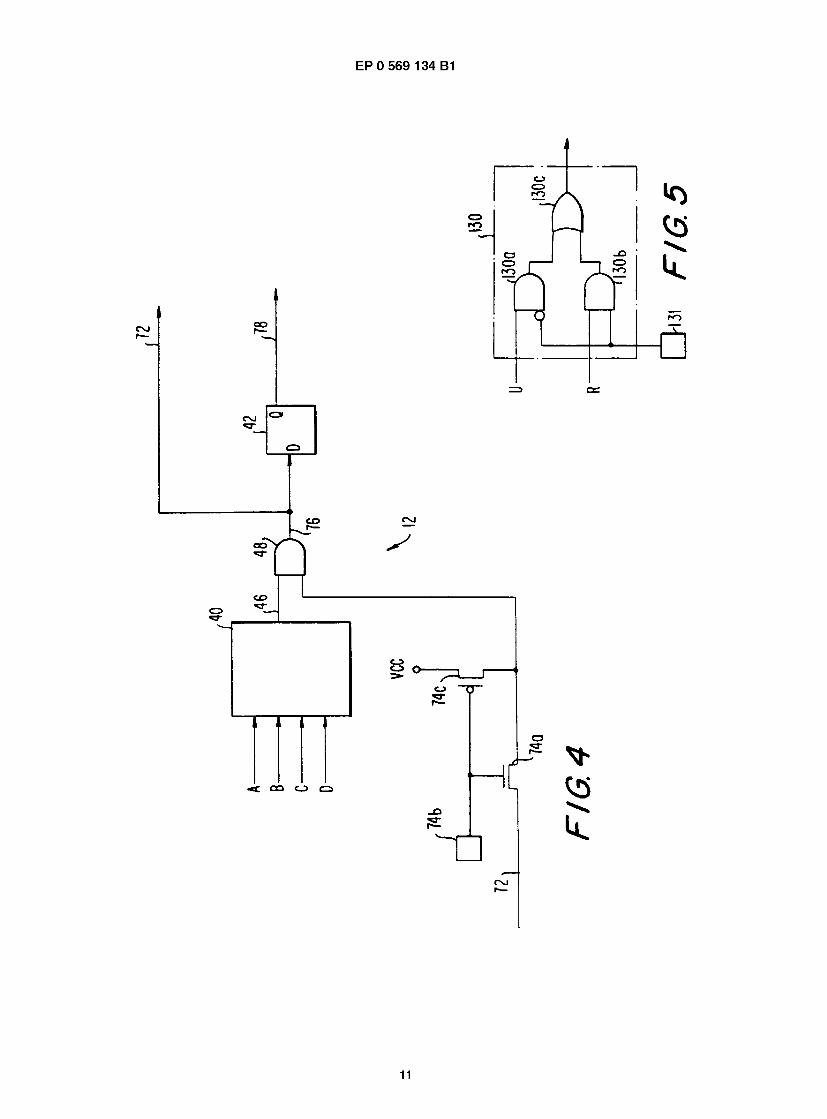
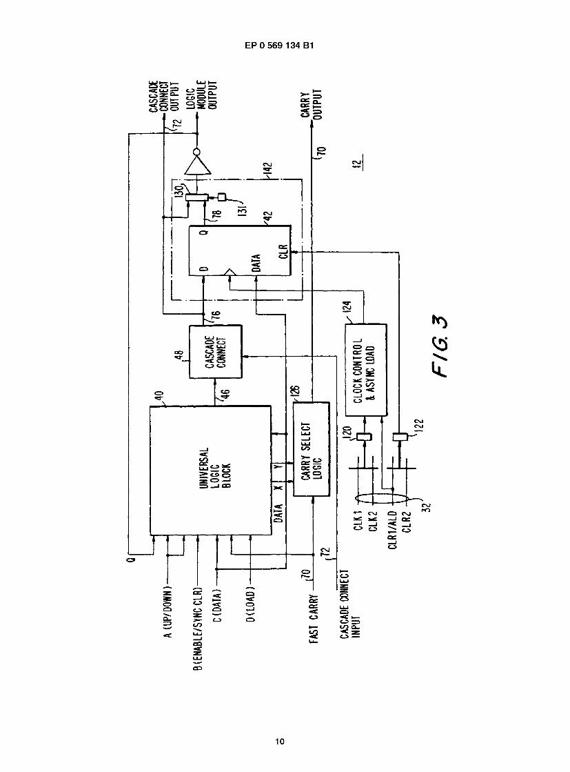
Atypical logic module 12 suitable for use in above- described circuit 1 0 and also embodying the present in-
fo vention is shown in FIG. 3. Universal logic block 40 is programmable to produce on output lead 46 an output signal which is one of several possible logical functions (preferably any possible logical function) of input signals A-D. To facilitate performing addition, subtraction, and/
is or counting, universal logic block 40 may also be pro- grammable to produce one of several possible logical functions of certain of inputs A-D and inputs Q and/or FAST CARRY. Universal logic block 40 can be imple- mented in any of several ways, for example, as a look
20 up table or a product-term-based macrocell. Output lead 46 is one input to cascade connect logic
element 48. For example, logic element 48 may be a two-input AND gate. The other input to logic element 48 is the cascade connect output 72 from another, preter-
ms ably adjacent, logic module 12 (see FIG. 2 which shows representative cascade connections 72a (between ad- jacent logic modules within an LAB) and 72b (between logic modules in adjacent LABs)). Assuming that this other input is active, logic element 48 logically combines
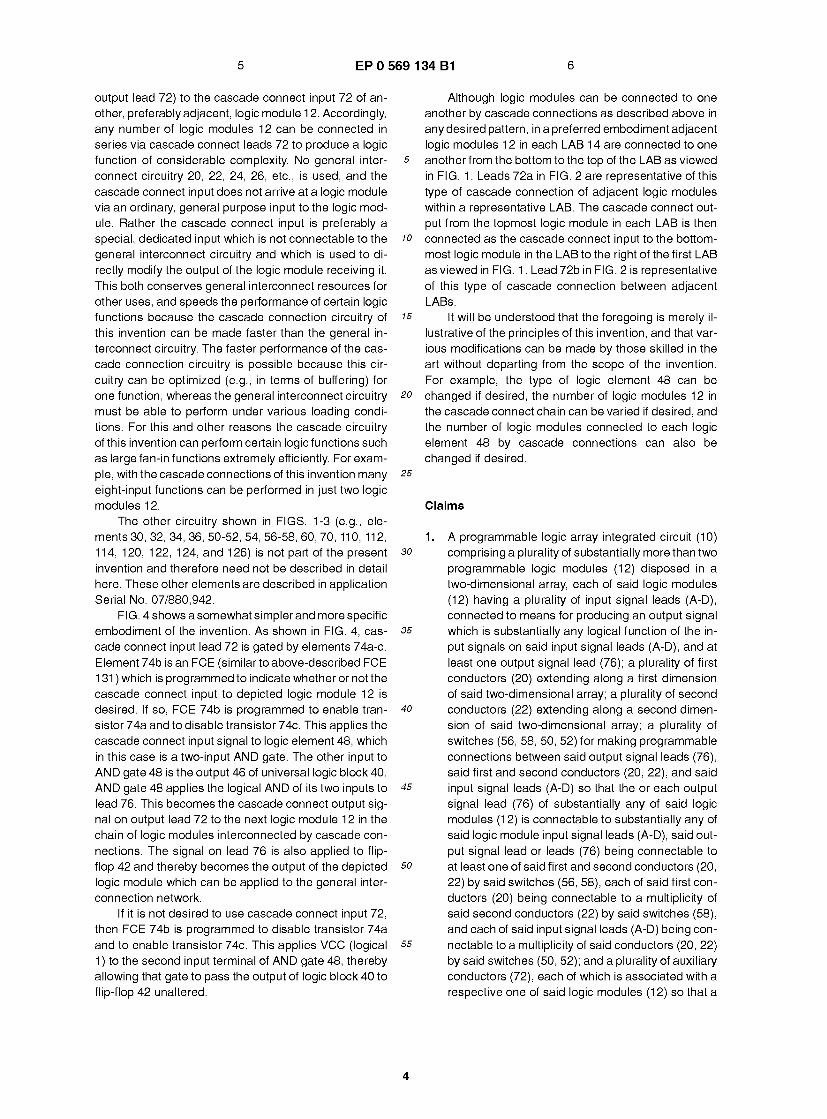
30 it with the signal on lead 46 and applies the resulting output signal via lead 76 to the D input of flip-flop 42. The Q output signal of flip-flop 42 is one input to switch 130. The signal on lead 76 is the other input to switch 130.
35 Switch 1 30 is controlled by a conventional program- mable function control element ("FCE") 131 to connect a desired one of its two inputs to its output. For example, FIG. 5 shows an illustrative embodiment of switch 130 including AND gates 1 30a and 1 30b and OR gate 1 30c.
40 The output of FCE 131 is applied to one input of AND gate 130b, and is also applied in inverted form to one input of AND gate 130a. Accordingly, either input U or input R appears at the output of OR gate 1 30c, depend- ing on the state of FCE 1 31 . In this way, the output signal
45 of cascade connect logic element 48 is passed by switch 130 either as registered by flip-flop 42 or unregistered by that flip-flop.
As is described in the immediately above-men- tioned application, FCE 1 31 can be implemented in any
so of several different ways, for example, as an SRAM, a DRAM, a cell of a first-in first-out ("FIFO") memory, an EPROM, an EEPROM, a function control register (as in Wahlstrom U.S. patent 3,473,160), a ferro-electric memory cell, a fuse (e.g., a laser fuse), an anti-fuse, or
55 the like. The output of switch 1 30 is inverted by the depicted
inverter and thereby becomes the output signal of the logic module. The signal on lead 76 is also applied (via
3
5 EP 0 569 134 B1 6
output lead 72) to the cascade connect input 72 of an- other, preferably adjacent, logic module 12. Accordingly, any number of logic modules 12 can be connected in series via cascade connect leads 72 to produce a logic function of considerable complexity. No general inter- connect circuitry 20, 22, 24, 26, etc., is used, and the cascade connect input does not arrive at a logic module via an ordinary, general purpose input to the logic mod- ule. Rather the cascade connect input is preferably a special, dedicated input which is not connectable to the general interconnect circuitry and which is used to di- rectly modify the output of the logic module receiving it. This both conserves general interconnect resources for other uses, and speeds the performance of certain logic functions because the cascade connection circuitry of this invention can be made faster than the general in- terconnect circuitry. The faster performance of the cas- cade connection circuitry is possible because this cir- cuitry can be optimized (e.g., in terms of buffering) for one function, whereas the general interconnect circuitry must be able to perform under various loading condi- tions. For this and other reasons the cascade circuitry of this invention can perform certain logic functions such as large fan-in functions extremely efficiently. For exam- ple, with the cascade connections of this invention many eight-input functions can be performed in just two logic modules 12.
The other circuitry shown in FIGS. 1-3 (e.g., ele- ments 30, 32, 34, 36,50-52, 54, 56-58, 60,70, 110, 112, 114, 120, 122, 124, and 126) is not part of the present invention and therefore need not be described in detail here. These other elements are described in application Serial No. 07/880,942.
Fl G. 4 shows a somewhat simpler and more specific embodiment of the invention. As shown in FIG. 4, cas- cade connect input lead 72 is gated by elements 74a-c. Element 74b is an FCE (similarto above-described FCE 1 31 ) which is programmed to indicate whether or not the cascade connect input to depicted logic module 12 is desired. If so, FCE 74b is programmed to enable tran- sistor 74a and to disable transistor 74c. This applies the cascade connect input signal to logic element 48, which in this case is a two-input AND gate. The other input to AND gate 48 is the output 46 of universal logic block 40. AND gate 48 applies the logical AND of its two inputs to lead 76. This becomes the cascade connect output sig- nal on output lead 72 to the next logic module 12 in the chain of logic modules interconnected by cascade con- nections. The signal on lead 76 is also applied to flip- flop 42 and thereby becomes the output of the depicted logic module which can be applied to the general inter- connection network.
If it is not desired to use cascade connect input 72, then FCE 74b is programmed to disable transistor 74a and to enable transistor 74c. This applies VCC (logical 1 ) to the second input terminal of AND gate 48, thereby allowing that gate to pass the output of logic block 40 to flip-flop 42 unaltered.
Although logic modules can be connected to one another by cascade connections as described above in any desired pattern, in a preferred embodiment adjacent logic modules 12 in each LAB 14 are connected to one
5 another from the bottom to the top of the LAB as viewed in FIG. 1 . Leads 72a in FIG. 2 are representative of this type of cascade connection of adjacent logic modules within a representative LAB. The cascade connect out- put from the topmost logic module in each LAB is then
10 connected as the cascade connect input to the bottom- most logic module in the LAB to the right of the first LAB as viewed in FIG. 1 . Lead 72b in FIG. 2 is representative of this type of cascade connection between adjacent LABs.
is It will be understood that the foregoing is merely il- lustrative of the principles of this invention, and that var- ious modifications can be made by those skilled in the art without departing from the scope of the invention. For example, the type of logic element 48 can be
20 changed if desired, the number of logic modules 12 in the cascade connect chain can be varied if desired, and the number of logic modules connected to each logic element 48 by cascade connections can also be changed if desired.
25
Claims
1. A programmable logic array integrated circuit (10) 30 comprising a plurality of substantially more than two
programmable logic modules (12) disposed in a two-dimensional array, each of said logic modules (12) having a plurality of input signal leads (A-D), connected to means for producing an output signal
35 which is substantially any logical function of the in- put signals on said input signal leads (A-D), and at least one output signal lead (76); a plurality of first conductors (20) extending along a first dimension of said two-dimensional array; a plurality of second
40 conductors (22) extending along a second dimen- sion of said two-dimensional array; a plurality of switches (56, 58, 50, 52) for making programmable connections between said output signal leads (76), said first and second conductors (20, 22), and said
45 input signal leads (A-D) so that the or each output signal lead (76) of substantially any of said logic modules (1 2) is connectable to substantially any of said logic module input signal leads (A-D), said out- put signal lead or leads (76) being connectable to
so at least one of said first and second conductors (20, 22) by said switches (56, 58), each of said first con- ductors (20) being connectable to a multiplicity of said second conductors (22) by said switches (58), and each of said input signal leads (A-D) being con-
55 nectable to a multiplicity of said conductors (20, 22) by said switches (50, 52); and a plurality of auxiliary conductors (72), each of which is associated with a respective one of said logic modules (12) so that a
4
7 EP 0 569 134 B1 8
logic module (12), and for substituting the resulting registered output signal (78) for the output signal (76) applied to said switches (56, 58).
substantial majority of said logic modules (1 2) have an associated auxiliary conductor (72), each of said auxiliary conductors (72, 72a, 72b) connecting the output signal lead (76) of the associated logic mod- ule (12) to another receiving logic module (12) s which in a substantial majority of cases has an as- sociated auxiliary conductor (72, 72a, 72b) con- necting its output signal lead (76) to yet another re- ceiving logic module (12), each of said auxiliary conductors (72, 72a, 72b) making its connection be- 10 tween the associated logic module (12) and the re- ceiving logic module (12) without making use of said first and second conductors (20; 22) or said input signal leads (A-D); wherein each of said logic mod- ules (12) in use produces an intermediate output 15 signal (46) which is said any of a plurality of logical functions of said input signals (A-D), characterized in that each of said logic modules (12) includes con- nect means (48) for selectively modifying the output signal on the output signal lead (76) of said logic 20 module (1 2) in accordance with the signal on its as- sociated auxiliary conductor (72, 72a, 72b) by logi- cally combining said intermediate output signal (46) of said logic module (12) and the signal received by said logic module (12) via said auxiliary conductor 25 (72) to produce said output signal (76) of said logic module (12).
2. The circuit defined in claim 1 further characterised by gate means (74a) for selectively preventing the 30 output signal (76) of each logic module (12), which is received via its associated auxiliary conductor (72, 72a, 72b), from being used by the connect means (48) associated with each receiving logic module (1 2) to modify the output signal (76) of said 35 receiving logic module (12).
3. The circuit defined in claim 2 further characterised by a programmable function control element (74b) for controlling said gate means (74a). 40
4. The circuit defined in any preceding claim further characterised in that the connect means (48) asso- ciated with each receiving logic module comprises a logic gate (48; Fig. 4) for logically combining the 45 signal received by said receiving logic module (12) via said auxiliary conductor (72) and the intermedi- ate output signal (46) of said receiving logic module (12).
50 5. The circuit defined in claim 4 further characterised
in that said logic gate (48) comprises an AND gate (48; FIG. 4).
6. The circuit defined in claim 1 further characterised 55 in that each of said receiving logic modules (12) fur- ther comprises flip-flop means (42) for selectively registering the output signal (76) of said receiving
Patentanspriiche
1. Eine integrierte, programmierbare Schaltung (19) mit logischen Feldern, mit einer Vielheit von we- sentlich mehralszwei programmierbaren logischen Modulen (12), die in je zweidimensionalen Feldern angeordnet sind; jedes logische Modul (12) hat eine Vielheit von Signaleingangsleitungen (A-D), ver- bunden mit Mitteln zur Erzeugung eines Ausgangs- signals, welches irgendeine logische Funktion der Eingangssignale an den Eingangen (A-D) darstellt, und wenigstens einer Ausgangssignalleitung (76); eine Vielheit erster Leiter (20) erstreckt sich langs einer ersten Dimension des zweidimensionalen Feldes; eine Vielheit zweiter Leiter (22) erstreckt sich langs einer zweiten Dimension des zweidimen- sionalen Feldes; eine Vielheit von Schaltern (56, 58, 50, 52) zur Herstellung programmierbarer Ver- bindungen zwischen den Ausgangssignalleitungen (76), den ersten und zweiten Leitern (20, 22) und den Eingangssignalleitungen (A-D), so dass jede Ausgangssignalleitung (76) der logischen Module (1 2) verbindbar ist mit im wesentlichen einem jeden der logischen Eingangssignalleitungen (A-D), die Ausgangssignalleitung oder -leitungen (76) ist/sind verbindbar mit wenigstens einem der ersten und zweiten Leitungen (20, 22) mittels der Schalter (56, 58), jeder der ersten Verbinder (20) ist verbindbar mit einer Vielheit von zweiten Leitern (22) mittels der Schalter (58), und jede der Eingangssignallei- tungen (A-D) ist verbindbar mit einer Vielheit der Leiter (20. 22) mittels der Schalter (50, 52); und eine Vielheit von Hilfsleitern (72), von denen jeder zuge- ordnet bzw. verbindbar ist mit einem der logischen Module (1 2), so dass eine wesentliche Mehrheit der logischen Module (12) einen zugeordneten Hilfslei- ter (72) haben, wobei jeder der Hilfsleiter (72, 72a, 72b) die Ausgangssignalleitung (76) des zugeord- neten logischen Moduls (12) mit einem anderen empfangenden logischen Modul (12) verbindet, welches in einer wesentlichen Mehrzahl der Falle einen Hilfsleiter (72, 72a, 72b) zugeordnet hat, wo- durch seine Ausgangssignalleitung (76) mit noch einem anderen empfangenden logischen Modul (12) verbunden ist, jeder der Hilfsleiter (72, 72a, 72b) stellt seine Verbindung her zwischen dem zu- geordneten logischen Modul (12) und dem empfan- genden logischen Modul (12), ohne Gebrauch zu machen von dem ersten und zweiten Leiter (20, 22) oder den Eingangssignalleitungen (A-D); wobei je- des der in Betrieb befindlichen Module (12) ein ver- mittelndes oder Zwischen-Ausgangssignal (46) er- zeugt, welches eines aus der besagten Vielzahl der
5
9 EP 0 569 134 B1 10
logischen Funktion der Eingangssignale (A-D) ist, dadurch gekennzeichnet, dass jedes der logischen Module (12) Verbindungsmittel (48) aufweist zur wahlweisen Modifizierung des Ausgangssignals auf der Ausgangssignalleitung (76) des logischen s Moduls (12), entsprechend dem Signal an seinem zugeordneten Hilfsleiter, dabei logisch kombinie- rend das Zwischen-Ausgangssignal (76) des logi- schen Moduls (12) und des von dem logischen Mo- dul (12) iiber den Hilfsleiter (72) empfangenen Si- 10 gnals zur Erzeugung des Ausgangssignals (76) des logischen Moduls (12).
2. Die Schaltung nach Anspruch 1, weiter gekenn- zeichnet durch Tor- bzw. Gattermittel (74a) zur se- 15 lektiven Verhinderung, dass das iiber seine Hilfslei- ter (72, 72a, 72b) empfangene Ausgangssignal (76) jedes logischen Moduls (12) von den Verbindungs- mitteln (48), die zugeordnet sind zu jedem empfan- genden logischen Mudul (12), zur Modifizierung 20 verwendet wird.
3. Die Schaltung nach Anspruch 2, weiter gekenn- zeichnet durch ein programmierbares Funktions- steuerelement (74b) zur Steuerung der Tormittel 25 (74a).
4. Die Schaltung nach irgendeinem der vorhergehen- den Anspriiche, weiter dadurch gekennzeichnet, dass die Verbindungsmittel (48), die jedem empfan- 30 genden logischen Modul zugeordnet sind, ein logi- sches Tor (48; Figur 4) enthalten, zur logischen Kombinierung des durch das empfangende logi- sche Mudul (12) iiber den besagten Hilfsleiter (72) empfangenen Signals und das Zwischen-Aus- 35 gangssignal (46) des empfangenden logischen Mo- duls (12).
5. Die Schaltung nach Anspruch 4, weiter dadurch ge- kennzeichnet, dass das logische Tor (48) ein Und- 40 Tor (48; Figur 4) aufweist.
6. Die Schaltung nach Anspruch 1 , weiter dadurch ge- kennzeichnet, dass das empfangende logische Mo- dul ferner Flip-flop-Mittel (42) umfasst zur wahlwei- 45 sen Registrierung oder Zahlung des Ausgangssi- gnals (76) des empfangenden logischen Moduls (12) und zum Ersatz des resultierenden registrier- ten Ausgangssignals (78) anstelle des an den Schaltern (56, 58) anliegenden Ausgangssignals so (76).
Revendications 55
1 . Circuit integre a reseau logique programmable (10) comprenant plusieurs modules logiques program- mables (12) en nombre sensiblement superieur a
deux et disposes selon un reseau a deux dimen- sions, chacun des dits modules logiques (12) pre- sentant une pluralite de conducteurs de signaux d'entree (A-D), relies a un moyen pour produire un signal de sortie qui est sensiblement toute fonction logique des signaux d'entree sur les dits conduc- teurs de signaux d'entree (A-D), et au moins un con- ducteur de signaux de sortie (76) ; plusieurs pre- miers conducteurs (20) s'etendant selon une pre- miere dimension du dit reseau a deux dimensions ; plusieurs seconds conducteurs (22) s'etendant se- lon une seconde dimension du dit reseau a deux dimensions ; plusieurs interrupteurs (56, 58, 50, 52) pour realiser des connexions programmables entre les dits conducteurs de signaux de sortie (76), les dits premier et second conducteurs (20,22), et les dits conducteurs de signaux d'entree (A-D) de facon que le ou chaque conducteur de signaux de sortie (76) de sensiblement n'importe lequel des dits mo- dules logiques (12) puisse peut etre connecte a sensiblement n'importe lequel des dits conducteurs (A-D) de signaux d'entree des modules logiques, le ou les conducteurs de signaux d'entree (76) pou- vant etre relies a I'un au moins des dits premier et second conducteurs (20,22) par les dits interrup- teurs (56, 58), chacun des dits premiers conduc- teurs (20) pouvant etre connecte a une multiplicity des dits seconds conducteurs (22) par les dits in- terrupteurs (58), et chacun des dits conducteurs de signaux d'entree (A-D) pouvant etre relie a une mul- tiplicity des dits conducteurs (20,22) par les dits in- terrupteurs (50,52) ; et une pluralite de conducteurs auxiliaires (72), dont chacun est associe respecti- vement avec I'un des dits modules logiques (1 2) de facon qu'une sensible majorite des dits modules lo- giques (12) aient un conducteur auxiliaire associe (72), chacun des dits conducteurs auxiliaires (72, 72a, 72b) reliant le conducteur de signal de sor- tie (76) du module logique associe (12) a un autre module logique recepteur (12) qui, dans une sensi- ble majorite des cas, presente un conducteur auxi- liaire associe (72, 72a, 72b) qui relie son conducteur de signaux de sortie (76) a encore un autre module logique recepteur (12), chacun des dits conduc- teurs auxiliaires (72, 72a, 72b) faisant sa connexion entre le module logique associe (12) et le module logique recepteur (12) sans utiliser les dits premier et second conducteurs (20,22) ou les dits conduc- teurs de signaux d'entree (A-D) ; dans lequel cha- cun des dits modules logiques (12) utilises produit un signal de sortie intermediate (46) qui est cons- titue par la dite n'importe laquelle fonction logique de la pluralite de fonctions logiques des dits signaux d'entree (A-D), caracterise en ce que chacun des dits modules logiques (12) comprend un moyen de connexion (48) pour modifier selectivement le si- gnal de sortie sur le conducteur de signaux de sortie (76) du module logique (12) en accord avec le si-
6

11 EP 0 569 134 B1 12
gnal sur son conducteur auxiliaire associe (72,72a, 72b) en combinant logiquement le dit signal de sor- tie intermediate (46) du dit module logique (12) et le signal recu par le dit module logique (12) par I'in- termediaire du dit conducteur auxiliaire (72) pour s produire le dit signal de sortie (76) du dit module logique (12).
2. Circuit selon la revendication 1 , caracterise de plus par un moyen de porte (74a) destine a empecher 10 selectivement le signal de sortie (76) de chaque module logique (12), qui est recu par I'intermediaire de son conducteur auxiliaire associe (72, 72a, 72b), d'etre utilise par le moyen de connexion (48) asso- cie a chaque module logique de reception (12) pour 15 modifier le signal de sortie (76) du dit module logi- que de reception (12).
3. Circuit selon la revendication 2, caracterise de plus par un element de controle a fonction programma- 20 ble (74b) pour controler le dit moyen de porte (74a).
4. Circuit selon I'une quelconque des revendications precedentes, caracterise en ce que le moyen de connexion (48) associe a chaque module logique 25 de reception comprend une porte logique (48;figure 4) pour combiner logiquement le signal recu par le dit module logique de reception (12) par I'interme- diaire du dit conducteur auxiliaire (72) et le signal de sortie intermediate (46) du dit module logique 30 de reception (12).
5. Circuit selon la revendication 4, caracterise de plus en ce que la dite porte logique (48) comprend une porte ET (48;figure4). 35
6. Circuit selon la revendication 1 , caracterise de plus en ce que chacun des dits modules logiques de re- ception (12) comprend de plus un moyen flip-flop (42) pour enregistrer selectivement le signal de sor- 40 tie (76) du dit module logique de reception (12), et pour substituer le signal de sortie enregistre resul- tant (78) au signal de sortie (76) applique aux dits interrupteurs (56,58).
7
EP 0 569 134 B1
rO
M I i l I Ml
MINI |
M ! I M i II M I I I I I i i
! II I I I I I I I I I
I ! I I M I I !
T t t t 3 j
I ' ' I
i I i i I I I I
iTTi
T f n H E
1
TEC
m i
o CVJ
"HE
m \
s i
B l
< 3
< -TEDC
T H E
CVJ J "J =L CVJ
4 CVJ z r
CVJ »a- CVJ <=> CO CVJ CNJ
8
EP 0 569 134 B1
n i
—i
—
CO
L i
I 1
i {
i