Embed Size (px)
Citation preview
ISSN:1369 7021 © Elsevier Ltd 2012JUNE 2012 | VOLUME 15 | NUMBER 6238
Properties of suspended graphene membranes
Graphene is a single layer of graphite, one atomic layer of carbon
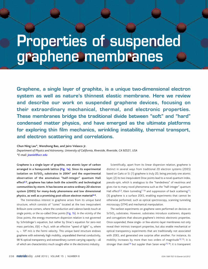
arranged in a honeycomb lattice (Fig. 1a). Since its experimental
isolation on Si/SiO2 substrates in 20041 and the experimental
observation of the anomalous “half-integer” quantum Hall
effect2,3, graphene has taken both the scientific and technological
communities by storm. It has become an extra-ordinary 2D electron
system (2DES) for many-body phenomena and low dimensional
physics, as well as a promising post-silicon electron material4-6.
The tremendous interest in graphene arises from its unique band
structure, which consists of “cones” located at the two inequivalent
Brillouin zone corners, where the conduction and valence bands touch at
single points, or the so-called Dirac points (Fig. 1b). In the vicinity of the
Dirac points, the energy-momentum dispersion relation is not governed
by Schrödinger’s equation, but rather by Dirac’s equation for zero-rest
mass particles, E(k) = h- vF k, with an effective “speed of light” vF, where
vF ~ 106 m/s is the Fermi velocity. This unique band structure endows
graphene with extremely high mobility, unparalleled thermal conductivity,
98 % optical transparency and extraordinary current-carrying capacity – all
of which are characteristics much sought-after in the electronics industry.
Scientifically, apart from its linear dispersion relation, graphene is
distinct in several ways from traditional 2D electron systems (2DES)
based on GaAs or Si: (1) graphene is truly 2D, being precisely one atomic
layer; (2) its two inequivalent Dirac points lead to a novel quantum index,
pseudo-spin, which is analogous to the “handedness” of neutrinos and
gives rise to many novel phenomena such as the “half-integer” quantum
Hall effect2,3, Klein tunneling7-10 and suppression of back scattering11;
(3) graphene is a surface 2DES, enabling experiments that cannot be
otherwise performed, such as optical spectroscopy, scanning tunneling
microscopy (STM) and mechanical manipulation.
The earliest experiments on graphene were performed on devices on
Si/SiO2 substrates. However, substrates introduce scatterers, dopants
and corrugations that obscure graphene’s intrinsic electronic properties.
Once suspended, these single- or few-atomic-layer membranes not only
reveal their intrinsic transport properties, but also enable mechanical or
optical transparency experiments that are traditionally not associated
with 2DES, and generated one surprise after another. For instance, its
mobility increases by more than two orders of magnitude12,13; it is
stronger than steel14 but suppler than Saran wrap15,16; it is transparent
Graphene, a single layer of graphite, is a unique two-dimensional electron system as well as nature’s thinnest elastic membrane. Here we review and describe our work on suspended graphene devices, focusing on their extraordinary mechanical, thermal, and electronic properties. These membranes bridge the traditional divide between “soft” and “hard” condensed matter physics, and have emerged as the ultimate platforms for exploring thin film mechanics, wrinkling instability, thermal transport, and electron scattering and correlations.
Chun Ning Lau*, Wenzhong Bao, and Jairo Velasco Jr.
Department of Physics and Astronomy, University of California, Riverside, Riverside, CA 92521, USA
*E-mail: [email protected]
MT156p238_245.indd 238 12/06/2012 10:14:08
Properties of suspended graphene membranes REVIEW
JUNE 2012 | VOLUME 15 | NUMBER 6 239
yet very conductive17,18; it conducts heat better than any other material.
Thus, suspended graphene membranes have become the ultimate
platform for exploring a wide variety of topics ranging from thin film
mechanics16,19-24, heat transport25-35, and electronic correlations36-45.
FabricationFabricating free-standing graphene devices is no easy feat, since these
single atomic layer membranes are exceedingly fragile to handle, while
the device geometry becomes ever more complex. For instance, transport
studies often require devices with top gates, which, together with back
gates, allow independent tuning of charge density and out-of-plane
electric field. In our laboratory we have developed two different methods
to fabricate suspended graphene devices with and without top gates.
In the first and more conventional technique, electrodes are deposited
on graphene sheets on Si/SiO2 substrates via standard electron-beam
lithography. If desired, a multi-level lithography technique is employed
to fabricate Cr top gates that are suspended ~100 – 300 nm above
graphene46,47. The completed devices are immersed in hydrofluoric acid
that partially removes the underlying SiO2 layer, then dried in a critical
point dryer12,13. These devices that undergo lithographical wet processes
typically have linear dimensions limited to 1 – 2 μm, and mobility ranging
from 20 000 to 150 000 cm2/Vs at low temperature. For comparison,
the low temperature mobility values of devices on Si/SiO2 substrates
are typically lower by an order of magnitude, ~2000 to 15 000 cm2/Vs.
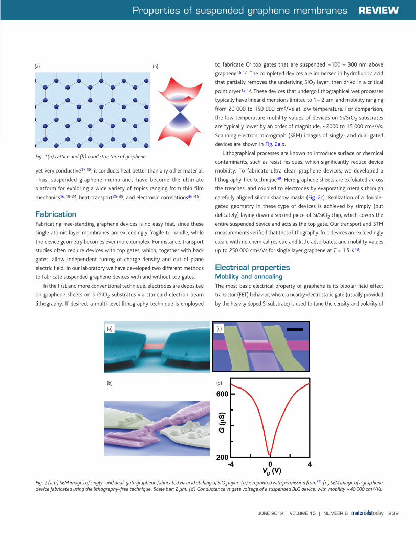
Scanning electron micrograph (SEM) images of singly- and dual-gated
devices are shown in Fig. 2a,b.
Lithographical processes are known to introduce surface or chemical
contaminants, such as resist residues, which significantly reduce device
mobility. To fabricate ultra-clean graphene devices, we developed a
lithography-free technique48. Here graphene sheets are exfoliated across
the trenches, and coupled to electrodes by evaporating metals through
carefully aligned silicon shadow masks (Fig. 2c). Realization of a double-
gated geometry in these type of devices is achieved by simply (but
delicately) laying down a second piece of Si/SiO2 chip, which covers the
entire suspended device and acts as the top gate. Our transport and STM
measurements verified that these lithography-free devices are exceedingly
clean, with no chemical residue and little adsorbates, and mobility values
up to 250 000 cm2/Vs for single layer graphene at T = 1.5 K48.
Electrical propertiesMobility and annealingThe most basic electrical property of graphene is its bipolar field effect
transistor (FET) behavior, where a nearby electrostatic gate (usually provided
by the heavily doped Si substrate) is used to tune the density and polarity of
Fig. 1(a) Lattice and (b) band structure of graphene.
(b)(a)
Fig. 2 (a,b) SEM images of singly- and dual-gate graphene fabricated via acid etching of SiO2 layer. (b) is reprinted with permission from67. (c) SEM image of a graphene device fabricated using the lithography-free technique. Scale bar: 2 μm. (d) Conductance vs gate voltage of a suspended BLG device, with mobility ~40 000 cm2/Vs.
(b)
(a) (c)
(d)
MT156p238_245.indd 239 12/06/2012 10:14:10
REVIEW Properties of suspended graphene membranes
JUNE 2012 | VOLUME 15 | NUMBER 6240
charge carriers in graphene, thereby modulating its conductance. For devices
on Si substrates with 300 nm of SiO2, 1 V in gate voltage Vg induces charge
density n ~ 7.2 × 10¹⁴ m-2; for typical suspended devices, the n/Vg ratio is
~2 × 10¹⁴ – 4 × 10¹⁴ m-2V-1. Fig. 2d displays the standard curve of device
conductivity σ vs. Vg, which is V-shaped, with a finite minimum conductivity
value σmin at the charge neutrality point (CNP), where graphene is undoped
with nominally zero charge. Graphene is hole- or p-doped at Vg < Vg,min
and electron- or n-doped at Vg > Vg,min. Away from the CNP, σ increases
approximately linearly with Vg; the slope of the σ(Vg) curve yields the field
effect mobility, μ = (1/e) dσ/dn, that characterizes the device quality. Here e
is electron charge and n is charge density. As mentioned above, μ ranges from
2000 – 15 000 cm2/Vs for devices supported on Si/SiO2 substrates, which are
generally considered mobility bottlenecks, as they introduce scatterings from
surface phonons, charge puddles that arise from charged impurities and/or
corrugations, and other neutral impurities.
By eliminating substrates, mobility of graphene devices increases
dramatically, with a mean free path as large as 1 μm13. One caveat is that
this is only achieved after a crucial current annealing step49, since mobility
of as-fabricated suspended graphene devices is limited by adsorbates and/or
resist residues. We find that the optimal annealing is typically achieved at
~ 0.2 mA/μm/layer at low temperature T = 4 K50. The temperature at the
center of the device is estimated to be ~ PL/8aK, where P is the Joule power,
L is the length, a is the cross-sectional area, and K is the thermal conductivity
of graphene. Using K ~ 600 W/mK (see section below), we estimate that the
center of graphene is annealed to ~ 500 K, which is hot enough to desorb
the resist residues and volatile adsorbates. After annealing, device mobility
at 4 K reaches 250 000 cm2/Vs for single layer graphene(SLG)13, and
350 000 – 500 000 for bilayer (BLG) and trilayer graphene (TLG) devices50-53.
Another insight into suspended graphene can be seen in the expression
for rs, the electronic interaction strength, which is approximately the ratio
of the inter-electron Coulomb energy to the Fermi energy. In graphene,
rs ∝n–(p–1)/2 / εr, where εr is the dielectric constant of the environment
and p is the power of the dispersion relation. Thus interaction-driven
phenomena are more easily accessed at low density and in suspended
graphene with εr = 1. Interestingly, compared to SLG, rs is much larger
in its few layer counterparts, since p = 1, 2, and 3 for SLG, BLG, and
rhombohedral-stacked TLG (see below), respectively6. Thus BLG and TLG
afford fascinating many-body physics, and in the rest of this section we
will focus on our experiments in these systems.
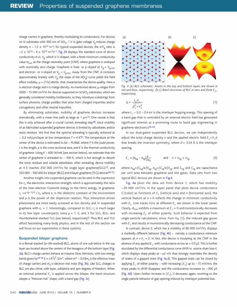
Suspended bilayer grapheneIn a Bernal-stacked (or AB-stacked) BLG, atoms of one sub-lattice in the top
layer are located above the centers of the hexagons of the bottom layer (Fig.
3a). BLG’s charge carriers behave as massive Dirac fermions, with low energy
bands given by54-56 E = ± h- 2k2 /2m*, where m* ~ 0.03me is the effective mass
of charge carriers and me is electron rest mass (Fig. 3b). Like SLG, charges in
BLG are also chiral, with layer, sublattice and spin degrees of freedom. When
an external potential V⊥ is applied across the bilayer, the band structure
adopts a “Mexican-hat” shape, with a band gap (Fig. 3c)
Δ = –√
⎢——t2⊥
t⊥——
V
+⊥— —
V⊥2
— (1)
where t⊥ ~ 0.2 – 0.4 eV is the interlayer hopping energy. This opening of
a band gap that is controlled by an external electric field has generated
significant interest as a promising route to band gap engineering in
graphene electronics56-64.
In our dual-gated suspended BLG devices, we can independently
adjust the total charge density n and the applied electric field E⊥=V⊥d
that breaks the inversion symmetry, where d = 3.34 Å is the interlayer
spacing,
E⊥ = (nbg – ntg) e—2ε0
–– and n = nbg + ntg, (2)
where nbg=(Cbg/e)Vbg, ntg=(Ctg/e)Vtg, and Cbg and Ctg are capacitance
per unit area between graphene and the gates. Data sets from two
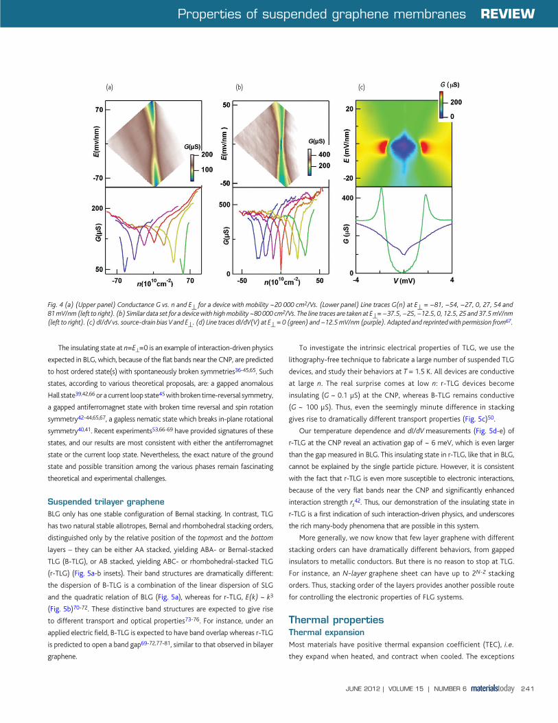
typical BLG devices are shown in Fig.4.
Fig. 4a plots the data set from device 1, which has mobility
~20 000 cm2/Vs. In the upper panel that plots device conductance
G (color) as functions of E⊥ (vertical axis) and n (horizontal axis), the
vertical feature at n = 0 reflects the change in minimum conductivity
with E⊥. Line traces G(n) at different E⊥ are shown in the lower panel.
Clearly, σmin exhibits a maximum at E⊥ = 0 and monotonically decreases
with increasing E⊥ of either polarity. Such behavior is expected from
single particle calculations, since, from Eq. (1), the induced gap grows
with E⊥ and results in monotonically decreasing conductance at the CNP.
In contrast, device 2, which has a mobility of 80 000 cm2/Vs, displays
a markedly different behavior (Fig. 4b) – namely a conductance minimum
appears at n = E⊥ = 0. In fact, this device is insulating at the CNP in the
absence of any applied E⊥, with conductance as low as < 0.5 μS. This is further
elucidated by the differential conductance curve dI/dV vs. source-drain bias V,
which displays sharp peaks at ~±2 mV that strongly resembles the density
of states of a gapped state (Fig. 4c,d). This gapped state can be closed by
applying E⊥ of either polarity – with increasing | E⊥| up to ~15 mV/nm, the
sharp peaks in dI/dV disappear and the conductance increases to ~300 μS
(Fig. 4d). Upon further increase in | E⊥|, G decreases again, reverting to the
single particle behavior of gap opening induced by interlayer potential bias.
Fig. 3 (a) BLG schematic. Atoms in the top and bottom layers are shown in red and blue, respectively. (b,c) Band structures of BLG in zero and finite E⊥, respectively.
(b)(a) (c)
MT156p238_245.indd 240 12/06/2012 10:14:13
Properties of suspended graphene membranes REVIEW
JUNE 2012 | VOLUME 15 | NUMBER 6 241
The insulating state at n=E⊥=0 is an example of interaction-driven physics
expected in BLG, which, because of the flat bands near the CNP, are predicted
to host ordered state(s) with spontaneously broken symmetries36-45,65. Such
states, according to various theoretical proposals, are: a gapped anomalous
Hall state39,42,66 or a current loop state45 with broken time-reversal symmetry,
a gapped antiferromagnet state with broken time reversal and spin rotation
symmetry42-44,65,67, a gapless nematic state which breaks in-plane rotational
symmetry40,41. Recent experiments53,66-69 have provided signatures of these
states, and our results are most consistent with either the antiferromagnet
state or the current loop state. Nevertheless, the exact nature of the ground
state and possible transition among the various phases remain fascinating
theoretical and experimental challenges.
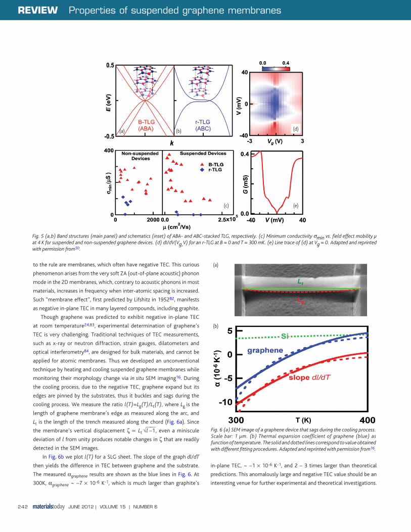
Suspended trilayer grapheneBLG only has one stable configuration of Bernal stacking. In contrast, TLG
has two natural stable allotropes, Bernal and rhombohedral stacking orders,
distinguished only by the relative position of the topmost and the bottom
layers – they can be either AA stacked, yielding ABA- or Bernal-stacked
TLG (B-TLG), or AB stacked, yielding ABC- or rhombohedral-stacked TLG
(r-TLG) (Fig. 5a-b insets). Their band structures are dramatically different:
the dispersion of B-TLG is a combination of the linear dispersion of SLG
and the quadratic relation of BLG (Fig. 5a), whereas for r-TLG, E(k) ~ k3
(Fig. 5b)70-72. These distinctive band structures are expected to give rise
to different transport and optical properties73-76. For instance, under an
applied electric field, B-TLG is expected to have band overlap whereas r-TLG
is predicted to open a band gap69-72,77-81, similar to that observed in bilayer
graphene.
To investigate the intrinsic electrical properties of TLG, we use the
lithography-free technique to fabricate a large number of suspended TLG
devices, and study their behaviors at T = 1.5 K. All devices are conductive
at large n. The real surprise comes at low n: r-TLG devices become
insulating (G ~ 0.1 μS) at the CNP, whereas B-TLG remains conductive
(G ~ 100 μS). Thus, even the seemingly minute difference in stacking
gives rise to dramatically different transport properties (Fig. 5c)50.
Our temperature dependence and dI/dV measurements (Fig. 5d-e) of
r-TLG at the CNP reveal an activation gap of ~ 6 meV, which is even larger
than the gap measured in BLG. This insulating state in r-TLG, like that in BLG,
cannot be explained by the single particle picture. However, it is consistent
with the fact that r-TLG is even more susceptible to electronic interactions,
because of the very flat bands near the CNP and significantly enhanced
interaction strength rs42. Thus, our demonstration of the insulating state in
r-TLG is a first indication of such interaction-driven physics, and underscores
the rich many-body phenomena that are possible in this system.
More generally, we now know that few layer graphene with different
stacking orders can have dramatically different behaviors, from gapped
insulators to metallic conductors. But there is no reason to stop at TLG.
For instance, an N-layer graphene sheet can have up to 2N-2 stacking
orders. Thus, stacking order of the layers provides another possible route
for controlling the electronic properties of FLG systems.
Thermal propertiesThermal expansionMost materials have positive thermal expansion coefficient (TEC), i.e.
they expand when heated, and contract when cooled. The exceptions
Fig. 4 (a) (Upper panel) Conductance G vs. n and E⊥ for a device with mobility ~20 000 cm2/Vs. (Lower panel) Line traces G(n) at E⊥ = −81, −54, −27, 0, 27, 54 and 81 mV/nm (left to right). (b) Similar data set for a device with high mobility ~80 000 cm2/Vs. The line traces are taken at E⊥= −37.5, −25, −12.5, 0, 12.5, 25 and 37.5 mV/nm (left to right). (c) dI/dV vs. source-drain bias V and E⊥. (d) Line traces dI/dV(V) at E⊥ = 0 (green) and −12.5 mV/nm (purple). Adapted and reprinted with permission from67.
(b)(a) (c)
MT156p238_245.indd 241 12/06/2012 10:14:14
REVIEW Properties of suspended graphene membranes
JUNE 2012 | VOLUME 15 | NUMBER 6242
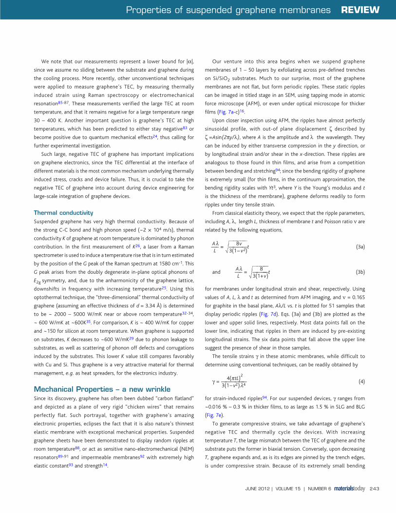
to the rule are membranes, which often have negative TEC. This curious
phenomenon arises from the very soft ZA (out-of-plane acoustic) phonon
mode in the 2D membranes, which, contrary to acoustic phonons in most
materials, increases in frequency when inter-atomic spacing is increased.
Such “membrane effect”, first predicted by Lifshitz in 195282, manifests
as negative in-plane TEC in many layered compounds, including graphite.
Though graphene was predicted to exhibit negative in-plane TEC
at room temperature24,83, experimental determination of graphene’s
TEC is very challenging. Traditional techniques of TEC measurements,
such as x-ray or neutron diffraction, strain gauges, dilatometers and
optical interferometry84, are designed for bulk materials, and cannot be
applied for atomic membranes. Thus we developed an unconventional
technique by heating and cooling suspended graphene membranes while
monitoring their morphology change via in situ SEM imaging16. During
the cooling process, due to the negative TEC, graphene expand but its
edges are pinned by the substrates, thus it buckles and sags during the
cooling process. We measure the ratio l(T)=Lg(T)/Lt(T), where Lg is the
length of graphene membrane’s edge as measured along the arc, and
Lt is the length of the trench measured along the chord (Fig. 6a). Since
the membrane’s vertical displacement ζ ∝ Lt √l —
–1—
, even a miniscule
deviation of l from unity produces notable changes in ζ that are readily
detected in the SEM images.
In Fig. 6b we plot l(T) for a SLG sheet. The slope of the graph dl/dT
then yields the difference in TEC between graphene and the substrate.
The measured αgraphene results are shown as the blue lines in Fig. 6. At
300K, αgraphene ~ –7 × 10⁻⁶ K-1, which is much larger than graphite’s
in-plane TEC, ~ –1 × 10⁻⁶ K-1, and 2 – 3 times larger than theoretical
predictions. This anomalously large and negative TEC value should be an
interesting venue for further experimental and theoretical investigations.
Fig. 5 (a,b) Band structures (main panel) and schematics (inset) of ABA- and ABC-stacked TLG, respectively. (c) Minimum conductivity σmin vs. field effect mobility μ at 4 K for suspended and non-suspended graphene devices. (d) dI/dV(Vg,V) for an r-TLG at B = 0 and T = 300 mK. (e) Line trace of (d) at Vg = 0. Adapted and reprinted with permission from50.
(b)(a)
(c)
(d)
(e)
Fig. 6 (a) SEM image of a graphene device that sags during the cooling process. Scale bar: 1 μm. (b) Thermal expansion coefficient of graphene (blue) as function of temperature. The solid and dotted lines correspond to value obtained with different fitting procedures. Adapted and reprinted with permission from16.
(a)
(b)
MT156p238_245.indd 242 12/06/2012 10:14:15
Properties of suspended graphene membranes REVIEW
JUNE 2012 | VOLUME 15 | NUMBER 6 243
We note that our measurements represent a lower bound for |α|,
since we assume no sliding between the substrate and graphene during
the cooling process. More recently, other unconventional techniques
were applied to measure graphene’s TEC, by measuring thermally
induced strain using Raman spectroscopy or electromechanical
resonation85-87. These measurements verified the large TEC at room
temperature, and that it remains negative for a large temperature range
30 – 400 K. Another important question is graphene’s TEC at high
temperatures, which has been predicted to either stay negative83 or
become positive due to quantum mechanical effects24, thus calling for
further experimental investigation.
Such large, negative TEC of graphene has important implications
on graphene electronics, since the TEC differential at the interface of
different materials is the most common mechanism underlying thermally
induced stress, cracks and device failure. Thus, it is crucial to take the
negative TEC of graphene into account during device engineering for
large-scale integration of graphene devices.
Thermal conductivitySuspended graphene has very high thermal conductivity. Because of
the strong C-C bond and high phonon speed (~2 × 10⁴ m/s), thermal
conductivity K of graphene at room temperature is dominated by phonon
contribution. In the first measurement of K26, a laser from a Raman
spectrometer is used to induce a temperature rise that is in turn estimated
by the position of the G peak of the Raman spectrum at 1580 cm-1. This
G peak arises from the doubly degenerate in-plane optical phonons of
E2g symmetry, and, due to the anharmonicity of the graphene lattice,
downshifts in frequency with increasing temperature25. Using this
optothermal technique, the “three-dimensional” thermal conductivity of
graphene (assuming an effective thickness of d = 3.34 Å) is determined
to be ~ 2000 – 5000 W/mK near or above room temperature32-34,
~ 600 W/mK at ~600K35. For comparison, K is ~ 400 W/mK for copper
and ~150 for silicon at room temperature. When graphene is supported
on substrates, K decreases to ~600 W/mK29 due to phonon leakage to
substrates, as well as scattering of phonon off defects and corrugations
induced by the substrates. This lower K value still compares favorably
with Cu and Si. Thus graphene is a very attractive material for thermal
management, e.g. as heat spreaders, for the electronics industry.
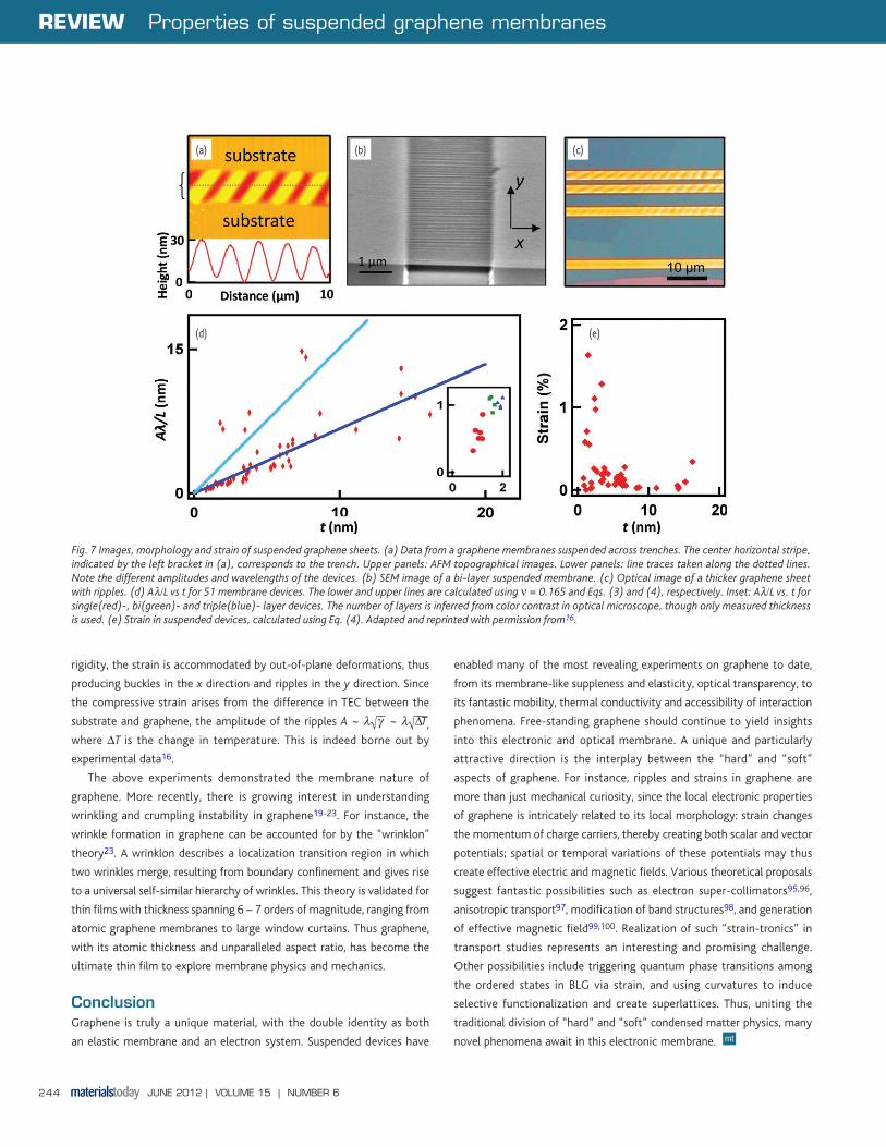
Mechanical Properties – a new wrinkleSince its discovery, graphene has often been dubbed “carbon flatland”
and depicted as a plane of very rigid “chicken wires” that remains
perfectly flat. Such portrayal, together with graphene’s amazing
electronic properties, eclipses the fact that it is also nature’s thinnest
elastic membrane with exceptional mechanical properties. Suspended
graphene sheets have been demonstrated to display random ripples at
room temperature88, or act as sensitive nano-electromechanical (NEM)
resonators89-91 and impermeable membranes92 with extremely high
elastic constant93 and strength14.
Our venture into this area begins when we suspend graphene
membranes of 1 – 50 layers by exfoliating across pre-defined trenches
on Si/SiO2 substrates. Much to our surprise, most of the graphene
membranes are not flat, but form periodic ripples. These static ripples
can be imaged in titled stage in an SEM, using tapping mode in atomic
force microscope (AFM), or even under optical microscope for thicker
films (Fig. 7a-c)16.
Upon closer inspection using AFM, the ripples have almost perfectly
sinusoidal profile, with out-of plane displacement ζ described by
ζ =Asin(2πy/λ), where A is the amplitude and λ the wavelength. They
can be induced by either transverse compression in the y direction, or
by longitudinal strain and/or shear in the x-direction. These ripples are
analogous to those found in thin films, and arise from a competition
between bending and stretching94; since the bending rigidity of graphene
is extremely small (for thin films, in the continuum approximation, the
bending rigidity scales with Yt3, where Y is the Young’s modulus and t
is the thickness of the membrane), graphene deforms readily to form
ripples under tiny tensile strain.
From classical elasticity theory, we expect that the ripple parameters,
including A, λ, length L, thickness of membrane t and Poisson ratio ν are
related by the following equations,
A—
λL– =
√⎪⎪—
—3(1
——
–8—
—vv
—
2)——
t (3a)
and A—
λL– =
√⎪⎪—
—3(1
——
+8—
—v
—
)——
t (3b)
for membranes under longitudinal strain and shear, respectively. Using
values of A, L, λ and t as determined from AFM imaging, and ν = 0.165
for graphite in the basal plane, Aλ/L vs. t is plotted for 51 samples that
display periodic ripples (Fig. 7d). Eqs. (3a) and (3b) are plotted as the
lower and upper solid lines, respectively. Most data points fall on the
lower line, indicating that ripples in them are induced by pre-existing
longitudinal strains. The six data points that fall above the upper line
suggest the presence of shear in those samples.
The tensile strains γ in these atomic membranes, while difficult to
determine using conventional techniques, can be readily obtained by
γ = —3(1
—4
–(π—
v2tL—
))2
—λ4— (4)
for strain-induced ripples94. For our suspended devices, γ ranges from
~0.016 % – 0.3 % in thicker films, to as large as 1.5 % in SLG and BLG
(Fig. 7e).
To generate compressive strains, we take advantage of graphene’s
negative TEC and thermally cycle the devices. With increasing
temperature T, the large mismatch between the TEC of graphene and the
substrate puts the former in biaxial tension. Conversely, upon decreasing
T, graphene expands and, as is its edges are pinned by the trench edges,
is under compressive strain. Because of its extremely small bending
MT156p238_245.indd 243 12/06/2012 10:14:17
REVIEW Properties of suspended graphene membranes
JUNE 2012 | VOLUME 15 | NUMBER 6244
rigidity, the strain is accommodated by out-of-plane deformations, thus
producing buckles in the x direction and ripples in the y direction. Since
the compressive strain arises from the difference in TEC between the
substrate and graphene, the amplitude of the ripples A ~ λ√γ–– ~ λ√Δ––T
–,
where ΔT is the change in temperature. This is indeed borne out by
experimental data16.
The above experiments demonstrated the membrane nature of
graphene. More recently, there is growing interest in understanding
wrinkling and crumpling instability in graphene19-23. For instance, the
wrinkle formation in graphene can be accounted for by the “wrinklon”
theory23. A wrinklon describes a localization transition region in which
two wrinkles merge, resulting from boundary confinement and gives rise
to a universal self-similar hierarchy of wrinkles. This theory is validated for
thin films with thickness spanning 6 – 7 orders of magnitude, ranging from
atomic graphene membranes to large window curtains. Thus graphene,
with its atomic thickness and unparalleled aspect ratio, has become the
ultimate thin film to explore membrane physics and mechanics.
ConclusionGraphene is truly a unique material, with the double identity as both
an elastic membrane and an electron system. Suspended devices have
enabled many of the most revealing experiments on graphene to date,
from its membrane-like suppleness and elasticity, optical transparency, to
its fantastic mobility, thermal conductivity and accessibility of interaction
phenomena. Free-standing graphene should continue to yield insights
into this electronic and optical membrane. A unique and particularly
attractive direction is the interplay between the “hard” and “soft”
aspects of graphene. For instance, ripples and strains in graphene are
more than just mechanical curiosity, since the local electronic properties
of graphene is intricately related to its local morphology: strain changes
the momentum of charge carriers, thereby creating both scalar and vector
potentials; spatial or temporal variations of these potentials may thus
create effective electric and magnetic fields. Various theoretical proposals
suggest fantastic possibilities such as electron super-collimators95,96,
anisotropic transport97, modification of band structures98, and generation
of effective magnetic field99,100. Realization of such “strain-tronics” in
transport studies represents an interesting and promising challenge.
Other possibilities include triggering quantum phase transitions among
the ordered states in BLG via strain, and using curvatures to induce
selective functionalization and create superlattices. Thus, uniting the
traditional division of “hard” and “soft” condensed matter physics, many
novel phenomena await in this electronic membrane.
Fig. 7 Images, morphology and strain of suspended graphene sheets. (a) Data from a graphene membranes suspended across trenches. The center horizontal stripe, indicated by the left bracket in (a), corresponds to the trench. Upper panels: AFM topographical images. Lower panels: line traces taken along the dotted lines. Note the different amplitudes and wavelengths of the devices. (b) SEM image of a bi-layer suspended membrane. (c) Optical image of a thicker graphene sheet with ripples. (d) Aλ/L vs t for 51 membrane devices. The lower and upper lines are calculated using ν = 0.165 and Eqs. (3) and (4), respectively. Inset: Aλ/L vs. t for single(red)-, bi(green)- and triple(blue)- layer devices. The number of layers is inferred from color contrast in optical microscope, though only measured thickness is used. (e) Strain in suspended devices, calculated using Eq. (4). Adapted and reprinted with permission from16.
(b)(a)
(d)
(c)
(e)
MT156p238_245.indd 244 12/06/2012 10:14:18
Properties of suspended graphene membranes REVIEW
JUNE 2012 | VOLUME 15 | NUMBER 6 245
REFERENCES
1. Novoselov, K. S., et al., Science (2004) 306, 666.
2. Novoselov, K. S., et al., Nature (2005) 438, 197.
3. Zhang, Y. B., et al., Nature (2005) 438, 201.
4. Castro Neto, A. H., et al., Rev Mod Phys (2009) 81, 109.
5. Fuhrer, M. S., et al., MRS Bulletin (2010) 35, 289.
6. Das Sarma, S., et al., Rev Mod Phys (2011) 83, 407.
7. Cheianov, V. V., and Fal’ko, V. I., Phys Rev B (2006) 74, 041403.
8. Katsnelson, M. I., et al., Nat Phys (2006) 2, 620.
9. Young, A. F., and Kim, P., Nat Phys (2009) 5, 222.
10. Stander, N., et al., Phys Rev Lett (2009) 102, 026807.
11. McEuen, P. L., et al., Phys Rev Lett (1999) 83, 5098.
12. Bolotin, K. I., et al., Sol State Commun (2008) 146, 351.
13. Du, X., et al., Nat Nanotechnol (2008) 3, 491.
14. Lee, C., et al., Science (2008) 321, 385.
15. Poot, M., and van der Zant, H. S. J., Appl Phys Lett (2008) 92, 063111.
16. Bao, W. Z., et al., Nat Nanotechnol (2009) 4, 562.
17. Mak, K. F., et al., Phys Rev Lett (2008) 101, 196405.
18. Nair, R. R., et al., Science (2008) 320, 1308.
19. Balankin, A. S., et al., Phys Rev E (2011) 84, 021118.
20. Min, K., and Aluru, N. R., Appl Phys Lett (2011) 98, 013113.
21. Paronyan, T. M., et al., ACS Nano (2011) 5, 9619.
22. Pereira, V. M., et al., Phys Rev Lett (2010) 105, 156603.
23. Vandeparre, H., et al., Phys Rev Lett (2011) 106, 224301.
24. Zakharchenko, K. V., et al., Phys Rev Lett (2009) 102, 046808.
25. Calizo, I., et al., Nano Lett (2007) 7, 2645.
26. Balandin, A. A., et al., Nano Lett (2008) 8, 902.
27. Chen, Z., et al., Appl Phys Lett (2009) 95, 161910.
28. Jang, W., et al., Nano Lett (2010) 10, 3909.
29. Seol, J. H., et al., Science (2010) 328, 213.
30. Wei, P., et al., Phys Rev Lett (2009) 102, 166808.
31. Zuev, Y. M., et al., Phys Rev Lett (2009) 102, 096807.
32. Ghosh, S., et al., Nat Mater (2010) 9, 555.
33. Murali, R., et al., Appl Phys Lett (2009) 94.
34. Cai, W. W., et al., Nano Lett (2010) 10, 1645.
35. Faugeras, C., et al., ACS Nano (2010) 4, 1889.
36. Min, H., et al., Phys Rev B (2008) 77, 041407.
37. Castro, E. V., et al., Phys Rev Lett (2008) 100, 186803.
38. Martin, I., et al., Phys Rev Lett (2008) 100, 036804.
39. Nandkishore, R., and Levitov, L., Phys Rev B (2010) 82, 115124.
40. Vafek, O., and Yang, K., Phys Rev B (2010) 81, 041401.
41. Lemonik, Y., et al., Phys Rev B (2010) 82, 201408.
42. Zhang, F., et al., Phys Rev Lett (2011) 106, 156801.
43. Jung, J., et al., Phys Rev B (2011) 83, 115408.
44. Kharitonov, M., preprint (2011) arXiv:1105.5386v1.
45. Zhu, L., et al., (2012) arXiv:1202.0821v1.
46. Liu, G., et al., Appl Phys Lett (2008) 92, 203103.
47. Velasco, J., et al., Phys Rev B (2010) 81, R121407.
48. Bao, W. Z., et al., Nano Res (2010) 3, 98.
49. Moser, J., et al., Appl Phys Lett (2007) 91, 163513.
50. Bao, W., et al., Nat Phys (2011) 7, 948.
51. Bao, W. Z., et al., Phys Rev Lett (2010) 105, 246601.
52. Bao, W., et al., Proc Natl Acad Sci U S A (2012) to appear.
53. Mayorov, A. S., et al., Science (2011) 333, 860.
54. McCann, E., Phys Rev B (2006) 74, 161403.
55. Novoselov, K. S., et al., Nat Phys (2006) 2, 177.
56. Castro, E. V., et al., Phys Rev Lett (2007) 99, 216802.
57. Oostinga, J. B., et al., Nat Mater (2008) 7, 151.
58. Kuzmenko, A. B., et al., Phys Rev B (2009) 165406.
59. Mak, K. F., et al., Phys Rev Lett (2009) 102, 256405.
60. Zhang, Y. B., et al., Nature (2009) 459, 820.
61. Xia, F. N., et al., Nano Lett (2010) 10, 715.
62. Taychatanapat, T., and Jarillo-Herrero, P., Phys Rev Lett (2010) 105, 166601.
63. Zou, K., and Zhu, J., Phys Rev B (2010) 081407.
64. Jing, L., et al., Nano Lett (2010) 10, 4000.
65. Zhang, F., et al., Phys Rev B (2010) 81, 041402 (R).
66. Weitz, R. T., et al., Science (2010) 330, 812.
67. Velasco, J., et al., Nature Nanotechnol (2012) 7, 156.
68. Martin, J., et al., Phys Rev Lett (2010) 105, 256806.
69. Freitag, F., et al., Phys Rev Lett (2012) 108, 076602.
70. Guinea, F., et al., Phys Rev B (2006) 73, 245426.
71. Aoki, M., and Amawashi, H., Sol State Commun (2007) 142, 123.
72. Zhang, F., et al., Phys Rev B (2010) 82, 035409.
73. Craciun, M. F., et al., Nat Nanotechnol (2009) 4, 383.
74. Lui, C. H., et al., Nat Phys (2011) 7, 944.
75. Taychatanapat, T., et al., Nat Phys (2011) 7, 621.
76. Zhang, L., et al., Nat Phys (2011) 7, 953.
77. Partoens, B., and Peeters, F. M., Phys Rev B (2006) 74, 075404.
78. Latil, S., and Henrard, L., Phys Rev Lett (2006) 97, 036803.
79. Koshino, M., and Ando, T., Phys Rev B (2007) 76, 085425.
80. Manes, J. L., et al., Phys Rev B (2007) 75, 155424.
81. Avetisyan, A. A., et al., Phys Rev B (2010) 81, 115432.
82. Lifshitz, I. M., Zh Eksp Teor Fiz (1952) 22, 475.
83. Mounet, N., and Marzari, N., Phys Rev B (2005) 71, 205214.
84. James, J. D., et al., Meas Sci Technol (2001) 12, R1.
85. Chen, C.-C., et al., Nano Lett (2009) 9, 4172.
86. Singh, V., et al., Nanotechnol (2010) 21, 165204.
87. Yoon, D., et al., Nano Lett (2011) 11, 3227.
88. Meyer, J. C., et al., Nature (2007) 446, 60.
89. Bunch, J. S., et al., Science (2007) 315, 490.
90. Garcia-Sanchez, D., et al., Nano Lett (2008) 8, 1399.
91. Chen, C. Y., et al., Nature Nanotechnol (2009) 4, 861.
92. Bunch, J. S., et al., Nano Lett (2008) 8, 2458.
93. Frank, I. W., et al., J Vac Sci Technol B (2007) 25, 2558.
94. Cerda, E., and Mahadevan, L., Phys Rev Lett (2003) 90, 074302.
95. Park, C. H., et al., Phys Rev Lett (2008) 101, 126804.
96. Park, C. H., et al., Nano Lett (2008) 8, 2920.
97. Park, C. H., et al., Nature Physics (2008) 4, 213.
98. Brey, L., and Fertig, H. A., Phys Rev Lett (2009) 103, 046809.
99. Guinea, F., et al., Nat Phys (2009) 6, 30.
100. Levy, N., et al., Science (2010) 329, 544.
AcknowledgementThe authors acknowledge the support by NSF CAREER DMR/0748910,
NSF DMR/1106358, NSF CBET/0756359, ONR N00014-09-1-0724,
ONR/DMEA H94003-10-2-1003 and the FENA Focus Center. CNL
acknowledges the support by the “Physics of Graphene” program at
KITP.
MT156p238_245.indd 245 12/06/2012 10:14:19


