Embed Size (px)
Citation preview
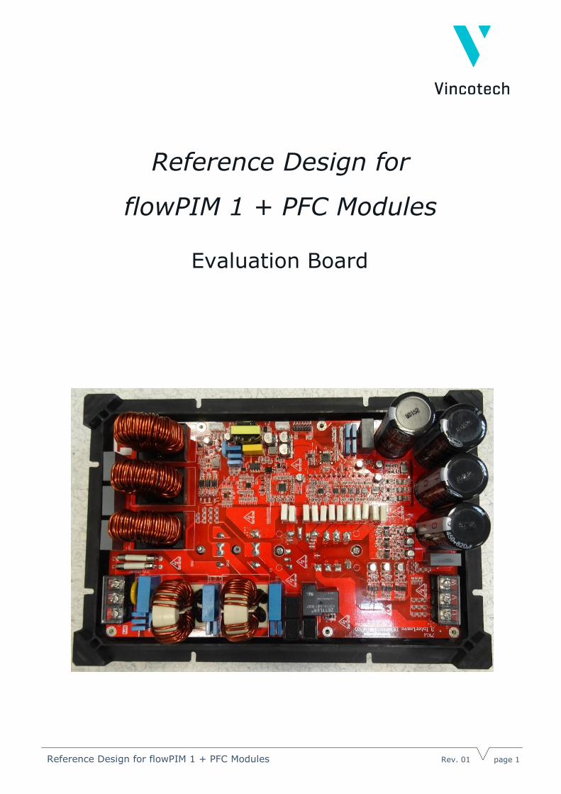
Reference Design for flowPIM 1 + PFC Modules Rev. 01 page 1
Reference Design for
flowPIM 1 + PFC Modules
Evaluation Board
Table of Contents
Reference Design for flowPIM 1 + PFC Modules Rev. 01 page 2
1 Abstract ........................................................................................................... 4
2 Introduction to LH9*-E08T family ........................................................................ 5
3 Introduction of the EVA board ............................................................................. 8
4 Design goals ..................................................................................................... 9
5 Circuit description .............................................................................................. 9
5.1 Line input ......................................................................................................... 9
5.2 Rectifier .......................................................................................................... 10
5.3 PFC ................................................................................................................. 11
5.3.1 Interleaved converters ...................................................................................... 11
5.3.2 PFC design ....................................................................................................... 12
5.4 Protection circuit .............................................................................................. 17
5.4.1 DEMAG protection ............................................................................................. 17
5.4.2 DC-link over voltage protection .......................................................................... 18
5.5 Three-Phase inverter ......................................................................................... 20
5.6 Interface to the MCU ......................................................................................... 23
5.6.1 Analog measurement ........................................................................................ 25
5.6.2 Communication ................................................................................................ 28
5.7 Auxiliary Power supply ...................................................................................... 29
6 Schematic........................................................................................................ 31
7 Hardware description ........................................................................................ 49
7.1 Dimensions and Board Layout ............................................................................ 50
8 BOM................................................................................................................ 55
9 References ....................................................................................................... 61

Revision History
Reference Design for flowPIM 1 + PFC Modules Rev. 01 page 3
Date Revision
Level Description
Page
Number(s)
2019.12.18 1 First release 63
2020.01.22 1.1 Document published 61
Disclaimer:
The information in this document is given as an indication for the purpose of implementation only and
shall not be regarded as any description or warranty of a certain functionality, condition or quality.
The statements contained herein, including any recommendation, suggestion or methodology, are to
be verified by the user before implementation, as operating conditions and environmental factors may
vary. It shall be the sole responsibility of the recipient of this document to verify any function
described herein in the given practical application. Vincotech GmbH hereby disclaims any and all
warranties and liabilities of any kind (including without limitation warranties of noninfringement of
intellectual property rights of any third party) with respect to any and all information given in this
document.
Safety Information
The board described is an evaluation board (EVA board) dedicated for laboratory
environment only.
It operates at high voltages. This board must be operated by qualified and skilled
personnel familiar with all applicable safety standards.
This EVA board can endanger life by exposure to rotating machinery and high voltages.
The ground potential of the EVA board is not floating it is biased to the negative DC-Link
voltage potential. In order to be able to measure by non-floating instrument (oscilloscope)
use isolation transformer at the AC input.
Allow at least 2 minutes for the DC-Link capacitor to discharge to safe voltage levels
(< 50 V).
Failure to follow these guidelines result personal injury or death and/or equipment
damage.
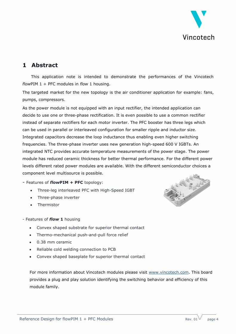
Reference Design for flowPIM 1 + PFC Modules Rev. 01 page 4
1 Abstract
This application note is intended to demonstrate the performances of the Vincotech
flowPIM 1 + PFC modules in flow 1 housing.
The targeted market for the new topology is the air conditioner application for example: fans,
pumps, compressors.
As the power module is not equipped with an input rectifier, the intended application can
decide to use one or three-phase rectification. It is even possible to use a common rectifier
instead of separate rectifiers for each motor inverter. The PFC booster has three legs which
can be used in parallel or interleaved configuration for smaller ripple and inductor size.
Integrated capacitors decrease the loop inductance thus enabling even higher switching
frequencies. The three-phase inverter uses new generation high-speed 600 V IGBTs. An
integrated NTC provides accurate temperature measurements of the power stage. The power
module has reduced ceramic thickness for better thermal performance. For the different power
levels different rated power modules are available. With the different semiconductor choices a
component level multisource is possible.
- Features of flowPIM + PFC topology:
Three-leg interleaved PFC with High-Speed IGBT
Three-phase inverter
Thermistor
- Features of flow 1 housing
Convex shaped substrate for superior thermal contact
Thermo-mechanical push-and-pull force relief
0.38 mm ceramic
Reliable cold welding connection to PCB
Convex shaped baseplate for superior thermal contact
For more information about Vincotech modules please visit www.vincotech.com. This board
provides a plug and play solution identifying the switching behavior and efficiency of this
module family.
Reference Design for flowPIM 1 + PFC Modules Rev. 01 page 5
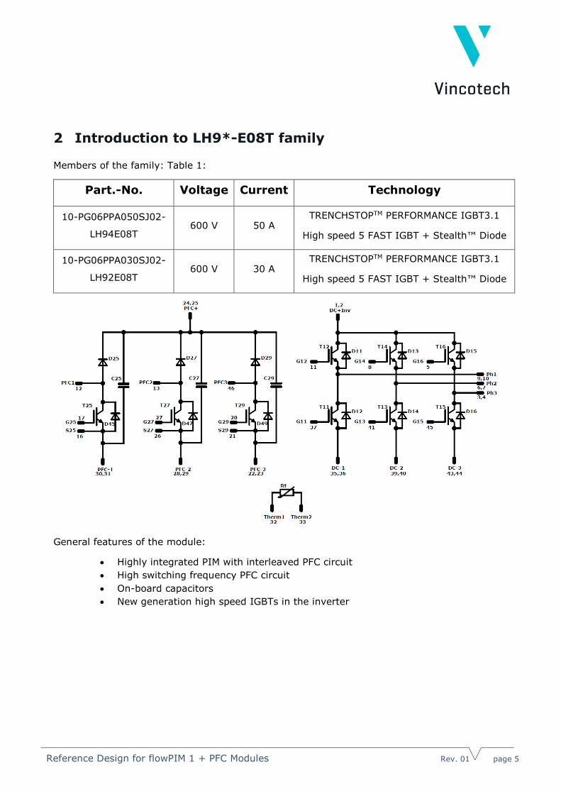
2 Introduction to LH9*-E08T family
Members of the family: Table 1:
Part.-No. Voltage Current Technology
10-PG06PPA050SJ02-
LH94E08T 600 V 50 A
TRENCHSTOPTM PERFORMANCE IGBT3.1
High speed 5 FAST IGBT + Stealth™ Diode
10-PG06PPA030SJ02-
LH92E08T 600 V 30 A
TRENCHSTOPTM PERFORMANCE IGBT3.1
High speed 5 FAST IGBT + Stealth™ Diode
General features of the module:
Highly integrated PIM with interleaved PFC circuit
High switching frequency PFC circuit
On-board capacitors
New generation high speed IGBTs in the inverter
Reference Design for flowPIM 1 + PFC Modules Rev. 01 page 6
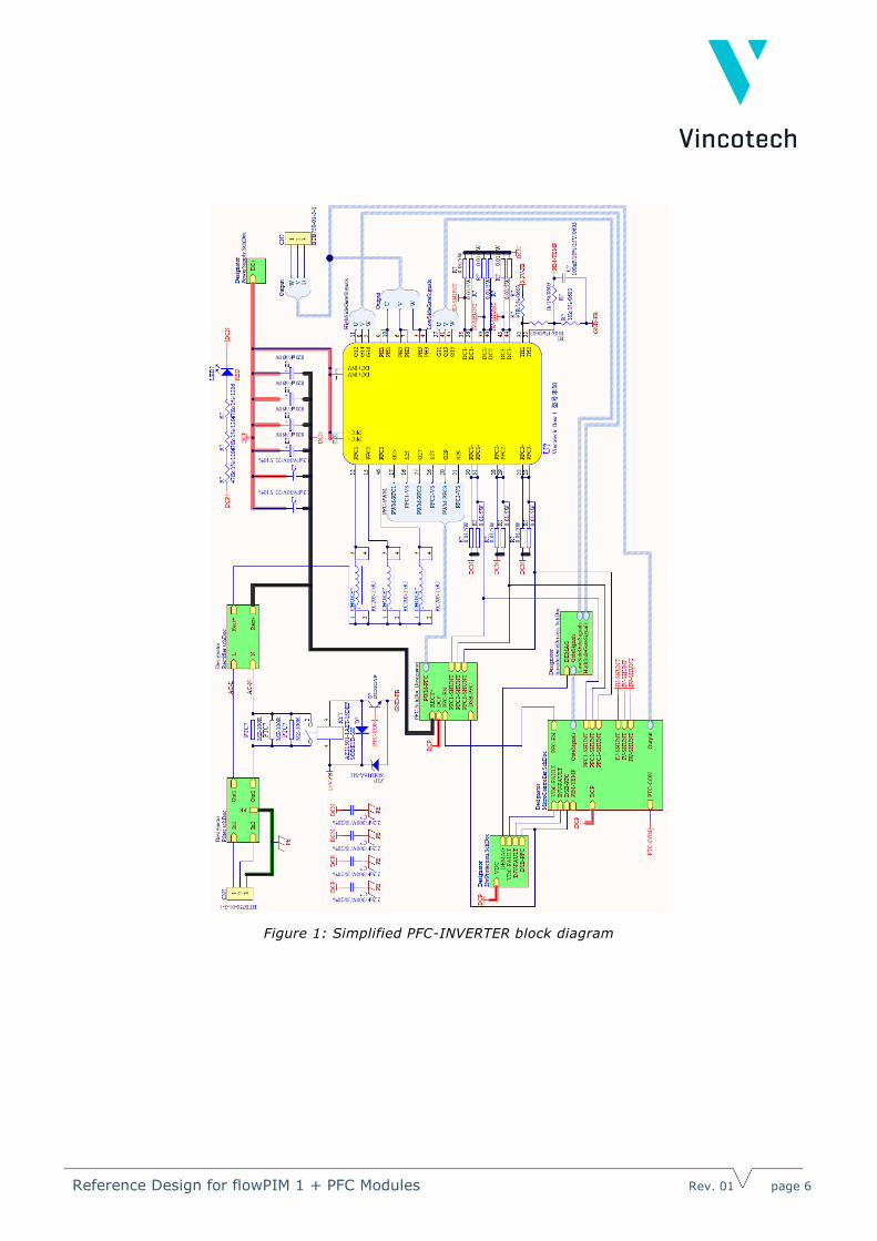
Figure 1: Simplified PFC-INVERTER block diagram
Reference Design for flowPIM 1 + PFC Modules Rev. 01 page 7
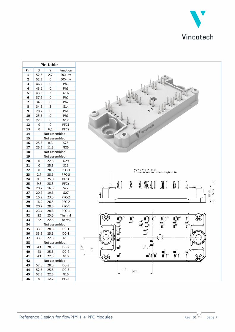
Pin table
Pin X Y Function
1 52,5 2,7 DC+Inv
2 52,5 0 DC+Inv
3 46,2 0 Ph3
4 43,5 0 Ph3
5 43,5 3 G16
6 37,2 0 Ph2
7 34,5 0 Ph2
8 34,5 3 G14
9 28,2 0 Ph1
10 25,5 0 Ph1
11 22,5 0 G12
12 0 0 PFC1
13 0 6,1 PFC2
14 Not assembled
15 Not assembled
16 25,5 8,3 S25
17 25,5 11,3 G25
18 Not assembled
19 Not assembled
20 0 22,5 G29
21 0 25,5 S29
22 0 28,5 PFC-3
23 2,7 28,5 PFC-3
24 9,8 25,8 PFC+
25 9,8 28,5 PFC+
26 20,7 16,5 S27
27 20,7 19,5 G27
28 16,9 23,5 PFC-2
29 16,9 26,5 PFC-2
30 20,7 28,5 PFC-1
31 23,4 28,5 PFC-1
32 22 25,5 Therm1
33 22 22,5 Therm2
34 Not assembled
35 33,5 28,5 DC-1
36 33,5 25,5 DC-1
37 33,5 22,5 G11
38 Not assembled
39 43 28,5 DC-2
40 43 25,5 DC-2
41 43 22,5 G13
42 Not assembled
43 52,5 28,5 DC-3
44 52,5 25,5 DC-3
45 52,5 22,5 G15
46 0 12,2 PFC3
Reference Design for flowPIM 1 + PFC Modules Rev. 01 page 8
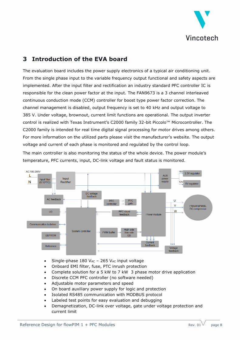
3 Introduction of the EVA board
The evaluation board includes the power supply electronics of a typical air conditioning unit.
From the single phase input to the variable frequency output functional and safety aspects are
implemented. After the input filter and rectification an industry standard PFC controller IC is
responsible for the clean power factor at the input. The FAN9673 is a 3 channel interleaved
continuous conduction mode (CCM) controller for boost type power factor correction. The
channel management is disabled, output frequency is set to 40 kHz and output voltage to
385 V. Under voltage, brownout, current limit functions are operational. The output inverter
control is realized with Texas Instrument’s C2000 family 32-bit Piccolo™ Microcontroller. The
C2000 family is intended for real time digital signal processing for motor drives among others.
For more information on the utilized parts please visit the manufacturer’s website. The output
voltage and current of each phase is monitored and regulated by the control loop.
The main controller is also monitoring the status of the whole device. The power module’s
temperature, PFC currents, input, DC-link voltage and fault status is monitored.
Single-phase 180 VAC – 265 VAC input voltage
Onboard EMI filter, fuse, PTC inrush protection
Complete solution for a 5 kW to 7 kW 3 phase motor drive application
Discrete CCM PFC controller (no software needed)
Adjustable motor parameters and speed
On board auxiliary power supply for logic and protection
Isolated RS485 communication with MODBUS protocol
Labeled test points for easy evaluation and debugging
Demagnetization, DC-link over voltage, gate under voltage protection and
current limit
Reference Design for flowPIM 1 + PFC Modules Rev. 01 page 9
4 Design goals
This application note illustrates the design process and component selection for a continuous
current mode power factor correction boost converter utilizing the FAN9673.
The three-phase inverter is controlled by TI’s C2000 MCU and driven by FAN73711MX gate
drivers. For the power stages the Vincotech’s 10-PG06PPA050SJ02-LH94E08T power module
is used.
Table 2: Technical specification
Parameter Symbol Test
condition
Min. Typ. Max. Unit Remarks
PFC Characteristics
AC input voltage VAC,IN 180 220 265 VRMS fin=47-63 Hz
Input frequency fLINE 47 63 Hz
DC-Link voltage VDC 385 VDC
PFC switching frequency fSW,PFC fSW,PFC 40 kHz
Inverter Characteristics
Inverter AC output
voltage
VOUT,AC 220 VAC 385V DC-Link
SPWM modulation
AC output current IOUT,AC VAC,IN≥
VAC,IN(Typ)
-55 55 Apk
5 Circuit description
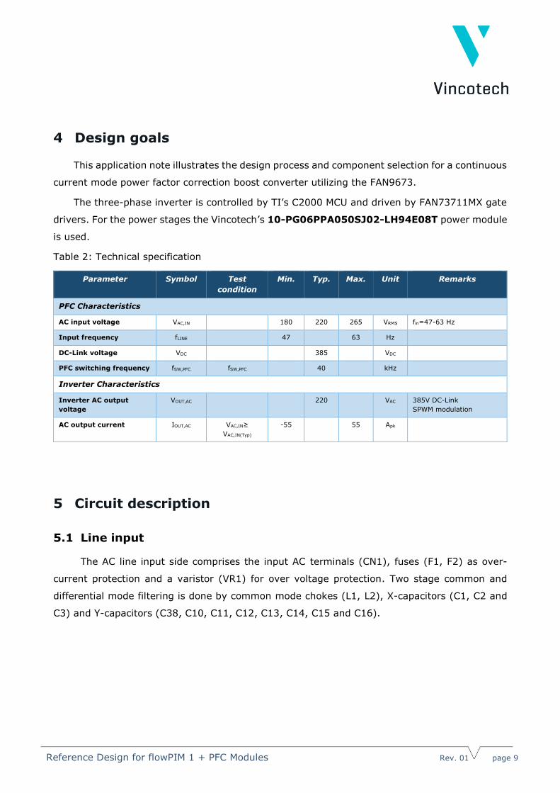
5.1 Line input
The AC line input side comprises the input AC terminals (CN1), fuses (F1, F2) as over-
current protection and a varistor (VR1) for over voltage protection. Two stage common and
differential mode filtering is done by common mode chokes (L1, L2), X-capacitors (C1, C2 and
C3) and Y-capacitors (C38, C10, C11, C12, C13, C14, C15 and C16).
Reference Design for flowPIM 1 + PFC Modules Rev. 01 page 10
The input inrush current caused by the charging current of the DC link capacitors is limited with
PTCs (PTC1, PTC2, and PTC3). If the capacitors are fully charged, the PTCs introduce unwanted
losses to the circuit. Therefore, the PTCs are bridged over with relay RY1. The relay is capable
to carry the current of the inverter (up to 50 A). The relay’s coil operates from 15 V supply.
Level shifting is done with an NPN digital transistor (Q1) which is connected to GPIO29.
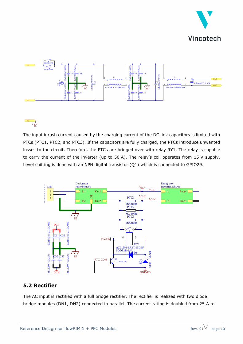
5.2 Rectifier
The AC input is rectified with a full bridge rectifier. The rectifier is realized with two diode
bridge modules (DN1, DN2) connected in parallel. The current rating is doubled from 25 A to
In1
In2
Out1
Out2
PE
F1
0325030MXP
F2
0325030MXP
VR
182
04
23
211
C1
1uF
/305V
/27.5
/10%
21
4 3
L1
LT38-4P-014/2.5mH-30A
C11
2.2
nF
/300V
/10/2
0%
C12
2.2
nF
/300V
/10/2
0%
C382.2
nF
/300V
/10/2
0%
C10
2.2
nF
/300V
/10/2
0%
C3
1uF/305V/27.5/10%C2
1uF
/305V
/27.5
/10%
C14
2.2
nF
/300V
/10/2
0%
C13
2.2
nF
/300V
/10/2
0%
C15
2.2
nF
/300
V/1
0/2
0%
C16
2.2
nF
/300
V/1
0/2
0%
21
4 3
L2
LT38-4P-014/2.5mH-30A
PE
PE PE
31
2 4
CHOKE3
RC20N15RJ
PFC112
PFC213
PFC346
G2517
S2516
G2727
S2726
G2920
S2921
PFC3-22
PFC2-28
PFC1-30
PFC1-31
PFC2-29
PFC3-23
PF
C+
24
PF
C+
25
TH132
TH233
DC
+IN
V1
DC
+IN
V2
G1211
G148
G165
PH19
PH110
PH26
PH27
PH33
PH34
G1137
G1341
G1545
DC1-35
DC1-36
DC2-39
DC2-40
DC3-43
DC3-44
U1Vincotech flow 1 power module
E4
820u
F/4
50
V
E3
820u
F/4
50
V
E2
820u
F/4
50
V
E1
820u
F/4
50
V
C18
2.2
uF
/630V
/22.5
/10%
C19
2.2
uF
/630V
/22.5
/10%
DCP
DCN
DCPR1
470k/1%/1206
R28
470k/1%/1206R24
470k/1%/1206
LED5
RED
DCN
123
CN2
BTB750-01-3-1C9
2.2
nF
/300V
/10/2
0%
C35
2.2
nF
/300V
/10/2
0%
C36
2.2
nF
/300V
/10/2
0%
C37
2.2
nF
/300V
/10/2
0%
PE
DCP
DCN
R6010.01/5W
R6020.01/5W
IU-SHUNT
R6040.01/5W
R603 0.01/5WIV-SHUNT
R6060.01/5W
R605 0.01/5W
DCN
IW-SHUNT
R1647R/1%/0603
3.3V-FB
R20
10
0k
/1%
/060
3
R2310k/1%/0603
GND-FB
R22
1k/1%/0603
C20100nF/10%/25V/0603
PIM-TEMP
R6070.01/5W
R608
0.01/5W
DCN
R6090.01/5W
R610
0.01/5W
DCN
R6110.01/5W
R612
0.01/5W
DCN
31
2 4
CHOKE1
RC20N15RJ
31
2 4
CHOKE2
RC20N15RJ
123
CN1
BT
B75
0-0
1-3
-1
PE
PTC1
MZ-100RPTC2
MZ-100RPTC3
MZ-100R
1 2
34
RY1AZ21501-1AET-15DEF
D1SODE1D-SH
15V-FB
ZD
1
SO
DJ1
6A
-SH
Q1DTDG23YP
GND-FB
L
N
Rect+
Rect-
DesignatorRectifier.schDoc
In1
In2
Out1
Out2
PE
DesignatorFilter.schDoc
AC-N
AC-L
PFC-ENINV-FAULT
DSB-PFC GateSignals
PIM-TEMP
VDC-FAULT
IW-SHUNT
IU-SHUNTIV-SHUNT
PFC3-SHUNT
PFC1-SHUNTPFC2-SHUNT
DCP
PTC-CON
RSTVDCIx-CMP
Vout
DesignatorMicroController.SchDoc
GateSignals
HighSideGateSignalsLowSideGateSignals
DEMAG
DesignatorInverterGateDrivers.SchDoc
DS
B-P
FC
DCP
PF
C-E
N
RECT+
PF
C3
-SH
UN
TP
FC
2-S
HU
NT
PF
C1
-SH
UN
T
PWM-PFC
DesignatorPFC.SchDoc
DC+
DesignatorPowerSupply.SchDoc
VDC-FAULT
VDC
INV-FAULT
DSB-PFCDEMAG
RST
Ix-CMP
DesignatorHwProtection.SchDoc
UVW
LowSideGateSignals
UVW
HighSideGateSignals
PFC1-VS
PFC2-VS
PFC3-VS
PWM-PFC1
PWM-PFC2
PWM-PFC3
PFC-PWM
DCP
IU-SHUNTIV-SHUNTIW-SHUNT
DCP
U
V
W
Output
UVW
Output
PIM-TEMP
PTC-CON
AC-L
AC-N
Output
Output
Output
Reference Design for flowPIM 1 + PFC Modules Rev. 01 page 11
50 A. The output of the rectifier is the input of the boost PFC stage. The output of the rectifier
is filtered with capacitors (C4, C5, and C17).
5.3 PFC
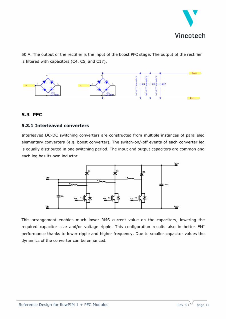
5.3.1 Interleaved converters
Interleaved DC-DC switching converters are constructed from multiple instances of paralleled
elementary converters (e.g. boost converter). The switch-on/-off events of each converter leg
is equally distributed in one switching period. The input and output capacitors are common and
each leg has its own inductor.
This arrangement enables much lower RMS current value on the capacitors, lowering the
required capacitor size and/or voltage ripple. This configuration results also in better EMI
performance thanks to lower ripple and higher frequency. Due to smaller capacitor values the
dynamics of the converter can be enhanced.
LN
Rect+
Rect-
C17
2.2
uF
/63
0V
/22.5
/10%
C5
2.2
uF
/63
0V
/22.5
/10%
C4
2.2
uF
/63
0V
/22.5
/10%
2
1
3
4
DN2D25XB80
2
1
3
4
DN1D25XB80
1
1
2
2
3
3
4
4
D D
C C
B B
A A
Proprietary data, company confidental. All rights reserved.Date:
Designed: Schematic
file name: 3phInterlavedPFC.SchDoc
11 /
PIMPFC-40
Kubinger
05.09.2019
D1
Cout
G1
Out-
Out+
IN+
T1
L1
IN-
D2
G2 T2
D3
G3 T3
L2
L3
Cin
Reference Design for flowPIM 1 + PFC Modules Rev. 01 page 12
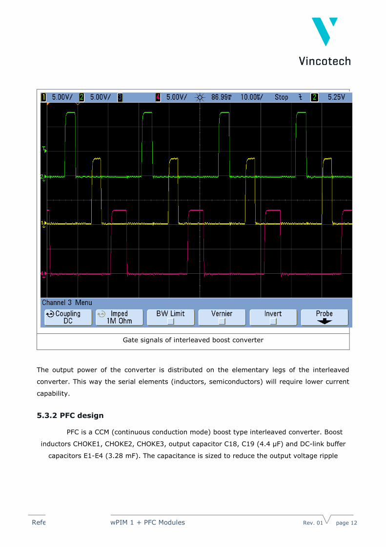
Gate signals of interleaved boost converter
The output power of the converter is distributed on the elementary legs of the interleaved
converter. This way the serial elements (inductors, semiconductors) will require lower current
capability.
5.3.2 PFC design
PFC is a CCM (continuous conduction mode) boost type interleaved converter. Boost
inductors CHOKE1, CHOKE2, CHOKE3, output capacitor C18, C19 (4.4 μF) and DC-link buffer
capacitors E1-E4 (3.28 mF). The capacitance is sized to reduce the output voltage ripple
Reference Design for flowPIM 1 + PFC Modules Rev. 01 page 13
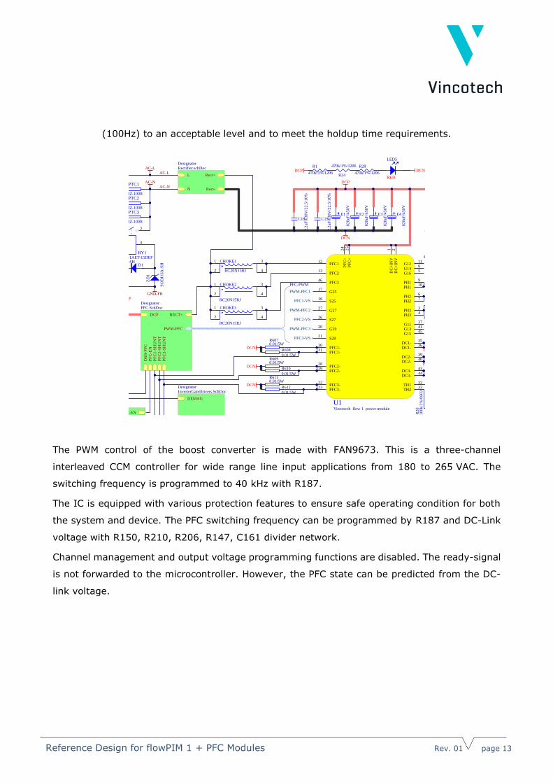
(100Hz) to an acceptable level and to meet the holdup time requirements.
The PWM control of the boost converter is made with FAN9673. This is a three-channel
interleaved CCM controller for wide range line input applications from 180 to 265 VAC. The
switching frequency is programmed to 40 kHz with R187.
The IC is equipped with various protection features to ensure safe operating condition for both
the system and device. The PFC switching frequency can be programmed by R187 and DC-Link
voltage with R150, R210, R206, R147, C161 divider network.
Channel management and output voltage programming functions are disabled. The ready-signal
is not forwarded to the microcontroller. However, the PFC state can be predicted from the DC-
link voltage.
31
2 4
CHOKE3
RC20N15RJ
PFC112
PFC213
PFC346
G2517
S2516
G2727
S2726
G2920
S2921
PFC3-22
PFC2-28
PFC1-30
PFC1-31
PFC2-29
PFC3-23
PF
C+
24
PF
C+
25
TH132
TH233
DC
+IN
V1
DC
+IN
V2
G1211
G148
G165
PH19
PH110
PH26
PH27
PH33
PH34
G1137
G1341
G1545
DC1-35
DC1-36
DC2-39
DC2-40
DC3-43
DC3-44
U1Vincotech flow 1 power module
E4
82
0uF
/450V
E3
82
0uF
/450V
E2
82
0uF
/450V
E1
82
0uF
/450V
C18
2.2
uF
/630V
/22.5
/10%
C19
2.2
uF
/630V
/22.5
/10%
DCP
DCN
DCPR1
470k/1%/1206
R28
470k/1%/1206R24
470k/1%/1206
LED5
RED
DCN
123
CN2
BTB750-01-3-1C9
2.2
nF
/30
0V
/10/2
0%
C35
2.2
nF
/30
0V
/10/2
0%
C36
2.2
nF
/300V
/10/2
0%
C37
2.2
nF
/300V
/10/2
0%
PE
DCP
DCN
R6010.01/5W
R6020.01/5W
IU-SHUNT
R6040.01/5W
R603 0.01/5WIV-SHUNT
R6060.01/5W
R605 0.01/5W
DCN
IW-SHUNT
R1647R/1%/0603
3.3V-FB
R20
100k
/1%
/060
3
R2310k/1%/0603
GND-FB
R22
1k/1%/0603
C20100nF/10%/25V/0603
PIM-TEMP
R6070.01/5W
R608
0.01/5W
DCN
R6090.01/5W
R610
0.01/5W
DCN
R6110.01/5W
R612
0.01/5W
DCN
31
2 4
CHOKE1
RC20N15RJ
31
2 4
CHOKE2
RC20N15RJ
123
CN1
BT
B75
0-0
1-3
-1
PE
PTC1
MZ-100RPTC2
MZ-100RPTC3
MZ-100R
1 2
34
RY1AZ21501-1AET-15DEF
D1SODE1D-SH
15V-FB
ZD
1
SO
DJ1
6A
-SH
Q1DTDG23YP
GND-FB
L
N
Rect+
Rect-
DesignatorRectifier.schDoc
In1
In2
Out1
Out2
PE
DesignatorFilter.schDoc
AC-N
AC-L
PFC-ENINV-FAULT
DSB-PFC GateSignals
PIM-TEMP
VDC-FAULT
IW-SHUNT
IU-SHUNTIV-SHUNT
PFC3-SHUNT
PFC1-SHUNTPFC2-SHUNT
DCP
PTC-CON
RSTVDCIx-CMP
Vout
DesignatorMicroController.SchDoc
GateSignals
HighSideGateSignalsLowSideGateSignals
DEMAG
DesignatorInverterGateDrivers.SchDoc
DS
B-P
FC
DCP
PF
C-E
N
RECT+
PF
C3
-SH
UN
TP
FC
2-S
HU
NT
PF
C1
-SH
UN
T
PWM-PFC
DesignatorPFC.SchDoc
DC+
DesignatorPowerSupply.SchDoc
VDC-FAULT
VDC
INV-FAULT
DSB-PFCDEMAG
RST
Ix-CMP
DesignatorHwProtection.SchDoc
UVW
LowSideGateSignals
UVW
HighSideGateSignals
PFC1-VS
PFC2-VS
PFC3-VS
PWM-PFC1
PWM-PFC2
PWM-PFC3
PFC-PWM
DCP
IU-SHUNTIV-SHUNTIW-SHUNT
DCP
U
V
W
Output
UVW
Output
PIM-TEMP
PTC-CON
AC-L
AC-N
Output
Output
Output
Reference Design for flowPIM 1 + PFC Modules Rev. 01 page 14
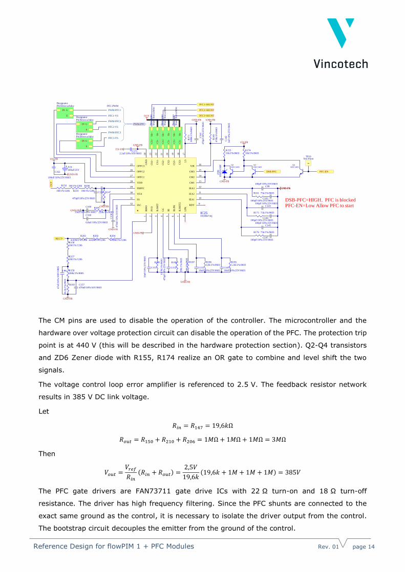
The CM pins are used to disable the operation of the controller. The microcontroller and the
hardware over voltage protection circuit can disable the operation of the PFC. The protection trip
point is at 440 V (this will be described in the hardware protection section). Q2-Q4 transistors
and ZD6 Zener diode with R155, R174 realize an OR gate to combine and level shift the two
signals.
The voltage control loop error amplifier is referenced to 2.5 V. The feedback resistor network
results in 385 V DC link voltage.
Let
𝑅𝑖𝑛 = 𝑅147 = 19,6𝑘Ω
𝑅𝑜𝑢𝑡 = 𝑅150 + 𝑅210 + 𝑅206 = 1𝑀Ω + 1𝑀Ω + 1𝑀Ω = 3𝑀Ω
Then
𝑉𝑜𝑢𝑡 =𝑉𝑟𝑒𝑓
𝑅𝑖𝑛
(𝑅𝑖𝑛 + 𝑅𝑜𝑢𝑡) =2,5𝑉
19,6𝑘(19,6𝑘 + 1𝑀 + 1𝑀 + 1𝑀) = 385𝑉
The PFC gate drivers are FAN73711 gate drive ICs with 22 Ω turn-on and 18 Ω turn-off
resistance. The driver has high frequency filtering. Since the PFC shunts are connected to the
exact same ground as the control, it is necessary to isolate the driver output from the control.
The bootstrap circuit decouples the emitter from the ground of the control.
OPFC325
OPFC226
OPFC127
VDD28
FBPFC29
VEA30
SS31
IAC32
BIB
O1
PV
O2
ILIM
IT3
GC
4
RI
5
RL
PK
6
ILIM
IT2
7
LP
K8
RDY9
IEA110
IEA211
IEA312
CM113
CM214
CM315
VIR16G
ND
24
CS
1+
23
CS
1-
22
CS
2+
21
CS
2-
20
CS
3+
19
CS
3-
18
LS
17
IC25FAN9673Q
C1712.2uF/10%/16V/0603
15V-FB
GND-FB
R17
124
9K
/1%
/06
03
C14
14
70
pF
/10
%/2
5V
/06
03
GND-FB
C1
42
1n
F/1
0%
/25V
/06
03
R14
847
0k/1
%/0
603
GND-FB
ZD
6U
DZ
5V
1B
F
R15510k/1%/0603
Q2KRC246S
15V-FB
GND-FB
Q3KRC246S
R17410k/1%/0603
Q4KRC246S
GND-FB
R1855.1K/1%/0603
C10510nF/10%/25V/0603
R18612K/1%/0603
C15110nF/10%/25V/0603
R187
20K
/1%
/06
03
R188
39K
/1%
/06
03
C152
470
pF
/10%
/25V
/060
3
GND-FB
R192
13
.7K
/1%
/06
03
GND-FB
C155
10
nF
/10
%/2
5V
/06
03
R1581M/1%/1206
R1571M/1%/1206
C98
47
nF
/10
%/1
00V
/08
05
R159200k/1%/0805
R160
16.2
k/1
%/0
60
3
C157470nF/10%/16V/0603
R204
4.02M/1%/1206
R202
4.02M/1%/1206
R203
4.02M/1%/1206
C1
58
47
0n
F/1
0%
/16
V/0
603
GND-FB
R205
220k/1%/0603
C100
33nF/10%/25V/0805GND-FB
C160
6.8nF/10%/25V/0603
R150
1M/1%/1206 R210
1M/1%/1206 R206
1M/1%/1206R147
19.6
k/1
%/0
603
GND-FB
C161
470pF/10%/25V/0603
E19100uF/25V
C162
100nF/10%/25V/0603
15V-FB
GND-FB
1
TP10Test Point
DSB-PFC=HIGH,PFC is blockedPFC-EN=Low Allow PFC to start
Sh+
Sh
-
CS
+
CS
-
Des
ignat
or
Sh
un
tFil
ter.
schd
oc
Sh+
Sh
-
CS
+
CS
-
Des
ignat
or
Sh
un
tFil
ter.
schd
oc
Sh+
Sh
-
CS
+
CS
-
Des
ignat
or
Sh
un
tFil
ter.
schd
oc
DCN
IN G
E
DesignatorPfcDriver.schdoc
IN G
E
DesignatorPfcDriver.schdoc
IN G
E
DesignatorPfcDriver.schdoc
DSB-PFC PFC-EN
RECT+
DC
P
PWM-PFC1
PFC1-VS
PWM-PFC2
PFC2-VS
PWM-PFC3
PFC3-VS
PFC-PWM
PFC2-SHUNT
PFC1-SHUNT
PFC3-SHUNT
PWM-PFC
GND-FB
R161 75k/1%/0603
C102100pF/10%/25V/0603
C99100pF/10%/25V/0603
GND-FB
R175 75k/1%/0603
C144100pF/10%/25V/0603
C143100pF/10%/25V/0603
R176 75k/1%/0603
C147100pF/10%/25V/0603
C145100pF/10%/25V/0603
Reference Design for flowPIM 1 + PFC Modules Rev. 01 page 15
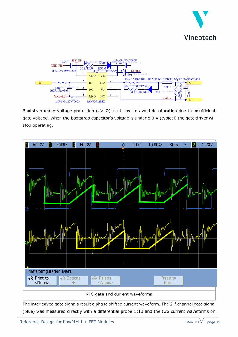
Bootstrap under voltage protection (UVLO) is utilized to avoid desaturation due to insufficient
gate voltage. When the bootstrap capacitor’s voltage is under 8.3 V (typical) the gate driver will
stop operating.
PFC gate and current waveforms
The interleaved gate signals result a phase shifted current waveform. The 2nd channel gate signal
(blue) was measured directly with a differential probe 1:10 and the two current waveforms on
IN G
E
VDD1
IN2
NC3
GND4
NC5
VS6
HO7
VB8
ICgd (ICgd_Designator21, ...)
FAN73711MX
Cdc (Cdc_Designator21, ...)
1uF/10%/50V/0805
GND-FB
15V-FBRbst (Rbst_Designator21, ...)
5.1R/1206
Dbst (Dbst_Designator21, ...)
HS1M
Ebst (Ebst_Designator21, ...)
100uF/25V
Cbst (Cbst_Designator21, ...)1uF/10%/50V/0805
Cin (Cin_Designator21, ...)
1nF/10%/25V/0603
GND-FB
Rin (Rin_Designator21, ...)
100R/1%/0603
Ron (Ron_Designator21, ...)22R/1206
Roff (Roff_Designator21, ...)100R/1206
Doff (Doff_Designator21, ...)SODE1D-SH
FBout (FBout_Designator21, ...)
BLM31PG121SZ1L
Cout
(Cout_
Des
ign
ator2
1, ..
.)
100pF/10%/25V/0603
Rout
(Rout_
Des
ign
ator2
1, ..
.)
33k/1
%/0
603
Emitter
Emitter
Reference Design for flowPIM 1 + PFC Modules Rev. 01 page 16
their corresponding test point. The current of the measured transistor (green) is rising when the
transistor is open, and zero when it is commutated to the boost diode. The output current of the
PFC stage is 10 A (3.3 A for each leg). Please note the high noise levels at the test points. This
is the result of the large ground loop created by probing the test points in the proximity of the
switching components. These points are primarily designed for the debugging of the
microcontroller without the high EMI from the power stage.
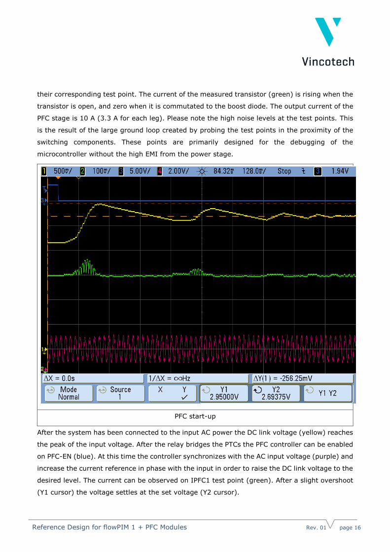
PFC start-up
After the system has been connected to the input AC power the DC link voltage (yellow) reaches
the peak of the input voltage. After the relay bridges the PTCs the PFC controller can be enabled
on PFC-EN (blue). At this time the controller synchronizes with the AC input voltage (purple) and
increase the current reference in phase with the input in order to raise the DC link voltage to the
desired level. The current can be observed on IPFC1 test point (green). After a slight overshoot
(Y1 cursor) the voltage settles at the set voltage (Y2 cursor).
Reference Design for flowPIM 1 + PFC Modules Rev. 01 page 17
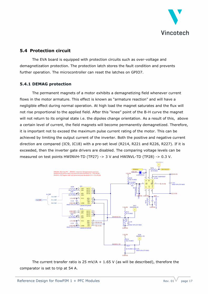
5.4 Protection circuit
The EVA board is equipped with protection circuits such as over-voltage and
demagnetization protection. The protection latch stores the fault condition and prevents
further operation. The microcontroller can reset the latches on GPIO7.
5.4.1 DEMAG protection
The permanent magnets of a motor exhibits a demagnetizing field whenever current
flows in the motor armature. This effect is known as “armature reaction” and will have a
negligible effect during normal operation. At high load the magnet saturates and the flux will
not rise proportional to the applied field. After this “knee” point of the B-H curve the magnet
will not return to its original state i.e. the dipoles change orientation. As a result of this, above
a certain level of current, the field magnets will become permanently demagnetized. Therefore,
it is important not to exceed the maximum pulse current rating of the motor. This can be
achieved by limiting the output current of the inverter. Both the positive and negative current
direction are compared (IC9, IC18) with a pre-set level (R214, R221 and R226, R227). If it is
exceeded, then the inverter gate drivers are disabled. The comparing voltage levels can be
measured on test points HWINVH-TD (TP27) -> 3 V and HWINVL-TD (TP28) -> 0.3 V.
The current transfer ratio is 25 mV/A + 1.65 V (as will be described), therefore the
comparator is set to trip at 54 A.
OUT11
OUT22
OUT314
OUT413
1IN+7
1IN-6
2IN+5
2IN-4
4IN+11
4IN-10
3IN+9
3IN-8
VCC3
GND12
IC9
LM2901AVQPWR
OUT11
OUT22
OUT314
OUT413
1IN+7
1IN-6
2IN+5
2IN-4
4IN+11
4IN-10
3IN+9
3IN-8
VCC3
GND12
IC18
LM2901AVQPWR
C124
100nF/10%/25V/0603GND-FB
3.3V-FB
C133
100nF/10%/25V/0603GND-FB
3.3V-FB
3.3V-FB
3.3V-FBGND-FB
R227
1k/1%/0603
GND-FB
R22610k/1%/0603
C135100nF/10%/25V/0603
R2
21
10
k/1
%/0
603
3.3V-FB
C129
100nF/10%/25V/0603
R2141k/1%/0603
SD4
D2
CP
3
VC
C14
GN
D7
Q5
RD1
Q6
IC16ASN74HC74MPWREP
3.3V-FB
C116100nF/10%/25V/0603
GND-FB
R2
12
20k/1
%/0
60
3
C128
1n
F/1
0%
/25
V/0
603
GND-FB
GND-FB
R20910k/1%/0603
C56
1nF
/10%
/25
V/0
603
R191
1k/1%/0603
D15L1SS355T1G
HWINVH-TD positive half cycle protection point threshold=3V=+55A-PEAK
HWINVL-TD Negative half cycle protection point threshold=0.3V=-55A-PEAK
DSB-PFC Blocking PFC DEMAG compressor demagnetization protection
R198
10k/1%/0603R38
10k/1%/0603
R40
10k/1%/0603
SD10
D12
CP
11
Q9
RD13
Q8
IC17BSN74HC74MPWREP
R2241M
/1%
/0603
R41
1K/1%/0603
GND-FB
3.3V-FB
1
TP18RST
1
TP19INV-FAULT
1
TP29DSB-PFC
1
TP28HWINVL-TD
1
TP27HWINVH-TD
SD10
D12
CP
11
Q9
RD13
Q8
IC16BSN74HC74MPWREP
D20
L1SS355T1G
GND-FB
3.3V-FB
1
TP30Test Point
HWINVL-TD
HWINVH-TD
RST
VDC
VDC-FAULT
DSB-PFC
INV-FAULTDEMAG
RST
3.3V-FB
3.3V-FB
GND-FB
GND-FB
DSB-PFC
DSB-PFC
3.3V-FB
GND-FB
3
21
84
IC12ATLV2316IPWR
GND-FB
GND-FB
C66
100nF/10%/25V/0603
GND-FB3.3V-FB
5
67
IC12BTLV2316IPWR
R8915k/1%/0603
R87
15k/1%/0603
C61100pF/10%/25V/0603
GND-FB
R76
1k/1%/06033.3V-FB
R77
10k/1%/0603
R88
2k/1%/0603
C68100pF/10%/25V/0603
GND-FB R9
01
M/1
%/0
60
3
SD4
D2
CP
3
VC
C14
GN
D7
Q5
RD1
Q6
IC17A
SN74HC74MPWREP
C69100nF/10%/25V/0603
GND-FB
3.3V-FB
R91
1k/1%/0603
GND-FB
R93
20
k/1
%/0
60
3
C7
01
nF
/10%
/25V
/0603
GND-FB
Hysteresis comparison voltage 3.1V=440VDC hardware protectionRegression voltage 2.83V=400VDC return
IU-CMP
IV-.CMP
IW-CMP
Ix-CMP
RST
Ix-CMP
1
TP20DSB-PFC
Reference Design for flowPIM 1 + PFC Modules Rev. 01 page 18
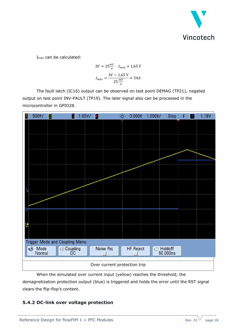
Imax can be calculated:
3𝑉 = 25𝑚𝑉
𝐴 ∙ 𝐼𝑚𝑎𝑥 + 1,65 V
𝐼𝑚𝑎𝑥 =3𝑉 − 1,65 V
25𝑚𝑉
𝐴
= 54𝐴
The fault latch (IC16) output can be observed on test point DEMAG (TP21), negated
output on test point INV-FAULT (TP19). The later signal also can be processed in the
microcontroller in GPIO28.
Over current protection trip
When the simulated over current input (yellow) reaches the threshold, the
demagnetization protection output (blue) is triggered and holds the error until the RST signal
clears the flip-flop’s content.
5.4.2 DC-link over voltage protection
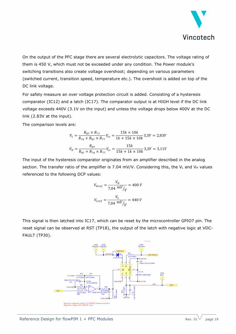
Reference Design for flowPIM 1 + PFC Modules Rev. 01 page 19
On the output of the PFC stage there are several electrolytic capacitors. The voltage rating of
them is 450 V, which must not be exceeded under any condition. The Power module’s
switching transitions also create voltage overshoot; depending on various parameters
(switched current, transition speed, temperature etc.). The overshoot is added on top of the
DC link voltage.
For safety measure an over voltage protection circuit is added. Consisting of a hysteresis
comparator (IC12) and a latch (IC17). The comparator output is at HIGH level if the DC link
voltage exceeds 440V (3.1V on the input) and unless the voltage drops below 400V at the DC
link (2.83V at the input).
The comparison levels are:
𝑉𝐿 =𝑅87 × 𝑅77
𝑅76 + 𝑅87 × 𝑅77
𝑉𝑐𝑐 =15𝑘 × 10𝑘
1𝑘 + 15𝑘 × 10𝑘3,3𝑉 = 2,83𝑉
𝑉𝐻 =𝑅87
𝑅87 + 𝑅76 × 𝑅77
𝑉𝑐𝑐 =15𝑘
15𝑘 + 1𝑘 × 10𝑘3,3𝑉 = 3,11𝑉
The input of the hysteresis comparator originates from an amplifier described in the analog
section. The transfer ratio of the amplifier is 7.04 mV/V. Considering this, the VL and VH values
referenced to the following DCP values:
𝑉𝐻𝑟𝑒𝑓 =𝑉𝐻
7,04 𝑚𝑉𝑉⁄
= 400 𝑉
𝑉𝐿𝑟𝑒𝑓 =𝑉𝐿
7,04 𝑚𝑉𝑉⁄
= 440 𝑉
This signal is then latched into IC17, which can be reset by the microcontroller GPIO7 pin. The
reset signal can be observed at RST (TP18), the output of the latch with negative logic at VDC-
FAULT (TP30).
OUT11
OUT22
OUT314
OUT413
1IN+7
1IN-6
2IN+5
2IN-4
4IN+11
4IN-10
3IN+9
3IN-8
VCC3
GND12
IC9
LM2901AVQPWR
OUT11
OUT22
OUT314
OUT413
1IN+7
1IN-6
2IN+5
2IN-4
4IN+11
4IN-10
3IN+9
3IN-8
VCC3
GND12
IC18
LM2901AVQPWR
C124
100nF/10%/25V/0603GND-FB
3.3V-FB
C133
100nF/10%/25V/0603GND-FB
3.3V-FB
3.3V-FB
3.3V-FBGND-FB
R227
1k/1%/0603
GND-FB
R22610k/1%/0603
C135100nF/10%/25V/0603
R221
10k/1
%/0
60
33.3V-FB
C129
100nF/10%/25V/0603
R2141k/1%/0603
SD4
D2
CP
3
VC
C1
4G
ND
7
Q5
RD1
Q6
IC16ASN74HC74MPWREP
3.3V-FB
C116100nF/10%/25V/0603
GND-FB
R212
20
k/1
%/0
603
C12
81nF
/10%
/25V
/060
3GND-FB
GND-FB
R20910k/1%/0603
C56
1n
F/1
0%
/25V
/060
3
R191
1k/1%/0603
D15L1SS355T1G
HWINVH-TD positive half cycle protection point threshold=3V=+55A-PEAK
HWINVL-TD Negative half cycle protection point threshold=0.3V=-55A-PEAK
DSB-PFC Blocking PFC DEMAG compressor demagnetization protection
R198
10k/1%/0603R38
10k/1%/0603
R40
10k/1%/0603
SD10
D12
CP
11
Q9
RD13
Q8
IC17BSN74HC74MPWREP
R2241M
/1%
/060
3
R41
1K/1%/0603
GND-FB
3.3V-FB
1
TP18RST
1
TP19INV-FAULT
1
TP29DSB-PFC
1
TP28HWINVL-TD
1
TP27HWINVH-TD
SD10
D1
2
CP
11
Q9
RD13
Q8
IC16BSN74HC74MPWREP
D20
L1SS355T1G
GND-FB
3.3V-FB
1
TP30Test Point
HWINVL-TD
HWINVH-TD
RST
VDC
VDC-FAULT
DSB-PFC
INV-FAULTDEMAG
RST
3.3V-FB
3.3V-FB
GND-FB
GND-FB
DSB-PFC
DSB-PFC
3.3V-FB
GND-FB
3
21
84
IC12ATLV2316IPWR
GND-FB
GND-FB
C66
100nF/10%/25V/0603
GND-FB3.3V-FB
5
67
IC12BTLV2316IPWR
R8915k/1%/0603
R87
15k/1%/0603
C61100pF/10%/25V/0603
GND-FB
R76
1k/1%/06033.3V-FB
R77
10k/1%/0603
R88
2k/1%/0603
C68100pF/10%/25V/0603
GND-FB R90
1M
/1%
/0603
SD4
D2
CP
3
VC
C14
GN
D7
Q5
RD1
Q6
IC17A
SN74HC74MPWREP
C69100nF/10%/25V/0603
GND-FB
3.3V-FB
R91
1k/1%/0603
GND-FB
R93
20k/1
%/0
603
C70
1nF
/10%
/25V
/0603
GND-FB
Hysteresis comparison voltage 3.1V=440VDC hardware protectionRegression voltage 2.83V=400VDC return
IU-CMP
IV-.CMP
IW-CMP
Ix-CMP
RST
Ix-CMP
1
TP20DSB-PFC
Reference Design for flowPIM 1 + PFC Modules Rev. 01 page 20
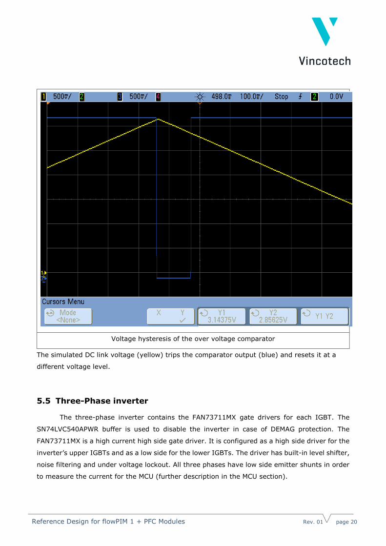
Voltage hysteresis of the over voltage comparator
The simulated DC link voltage (yellow) trips the comparator output (blue) and resets it at a
different voltage level.
5.5 Three-Phase inverter
The three-phase inverter contains the FAN73711MX gate drivers for each IGBT. The
SN74LVC540APWR buffer is used to disable the inverter in case of DEMAG protection. The
FAN73711MX is a high current high side gate driver. It is configured as a high side driver for the
inverter’s upper IGBTs and as a low side for the lower IGBTs. The driver has built-in level shifter,
noise filtering and under voltage lockout. All three phases have low side emitter shunts in order
to measure the current for the MCU (further description in the MCU section).
Reference Design for flowPIM 1 + PFC Modules Rev. 01 page 21
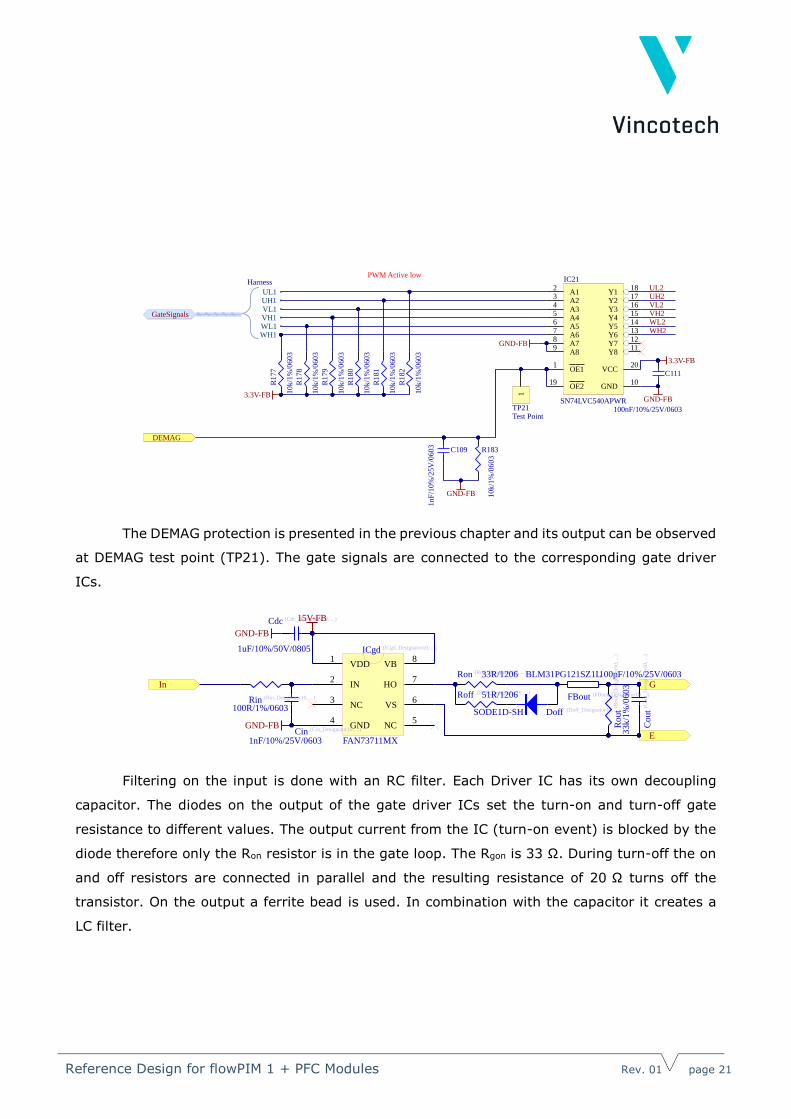
The DEMAG protection is presented in the previous chapter and its output can be observed
at DEMAG test point (TP21). The gate signals are connected to the corresponding gate driver
ICs.
Filtering on the input is done with an RC filter. Each Driver IC has its own decoupling
capacitor. The diodes on the output of the gate driver ICs set the turn-on and turn-off gate
resistance to different values. The output current from the IC (turn-on event) is blocked by the
diode therefore only the Ron resistor is in the gate loop. The Rgon is 33 Ω. During turn-off the on
and off resistors are connected in parallel and the resulting resistance of 20 Ω turns off the
transistor. On the output a ferrite bead is used. In combination with the capacitor it creates a
LC filter.
U
V
W
DCN
DCN
DCN
A12
A23
OE11
GND10
VCC20
A34
A45
A56
A67
A78
A89
OE219
Y118
Y217
Y316
Y415
Y514
Y613
Y712
Y811
IC21
SN74LVC540APWR
GND-FB
C111
100nF/10%/25V/0603
GND-FB
3.3V-FB
R1
79
10
k/1
%/0
60
3
R1
80
10
k/1
%/0
60
3
R1
81
10
k/1
%/0
60
3
R1
82
10
k/1
%/0
60
3
R1
78
10
k/1
%/0
60
3
R1
77
10
k/1
%/0
60
3
R183
10k
/1%
/06
03
C109
1nF
/10%
/25V
/0603
PWM Active low
3.3V-FB 1
TP21Test Point
UL1UH1VL1VH1WL1WH1
Harness
GateSignals
UL2UH2VL2VH2WL2WH2
UL2
VL2
WL2 WH2
VH2
UH2
In G
E
DesignatorHiSideDriver.schdoc
In G
E
DesignatorHiSideDriver.schdoc
In G
E
DesignatorHiSideDriver.schdoc
In G
E
Designator
LowSideDriver.schdoc
In G
E
Designator
LowSideDriver.schdoc
In G
E
Designator
LowSideDriver.schdoc
DEMAG
U
W
V
HighSideGateSignals
U
W
V
LowSideGateSignals
LowSideGateSignals HighSideGateSignals
GND-FB
In G
E
VDD1
IN2
NC3
GND4
NC5
VS6
HO7
VB8
ICgd (ICgd_Designator10, ...)
FAN73711MX
Cdc (Cdc_Designator10, ...)
1uF/10%/50V/0805
GND-FB
15V-FB
Cin (Cin_Designator10, ...)
1nF/10%/25V/0603
GND-FB
Rin (Rin_Designator10, ...)
100R/1%/0603
Ron (Ron_Designator10, ...)33R/1206
Roff (Roff_Designator10, ...)51R/1206
Doff (Doff_Designator10, ...)SODE1D-SH
FBout (FBout_Designator10, ...)
BLM31PG121SZ1L
Cout
(Co
ut_
Des
ignat
or1
0,
...)
100pF/10%/25V/0603
Rout
(Ro
ut_
Des
ignat
or1
0,
...)
33k/1
%/0
603
Reference Design for flowPIM 1 + PFC Modules Rev. 01 page 22
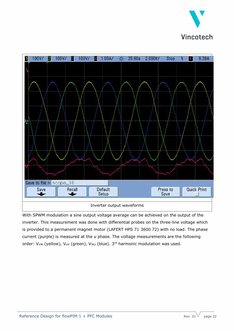
Inverter output waveforms
With SPWM modulation a sine output voltage average can be achieved on the output of the
inverter. This measurement was done with differential probes on the three-line voltage which
is provided to a permanent magnet motor (LAFERT HPS 71 3600 72) with no load. The phase
current (purple) is measured at the u phase. The voltage measurements are the following
order: VVW (yellow), VUV (green), VWU (blue). 3rd harmonic modulation was used.
Reference Design for flowPIM 1 + PFC Modules Rev. 01 page 23
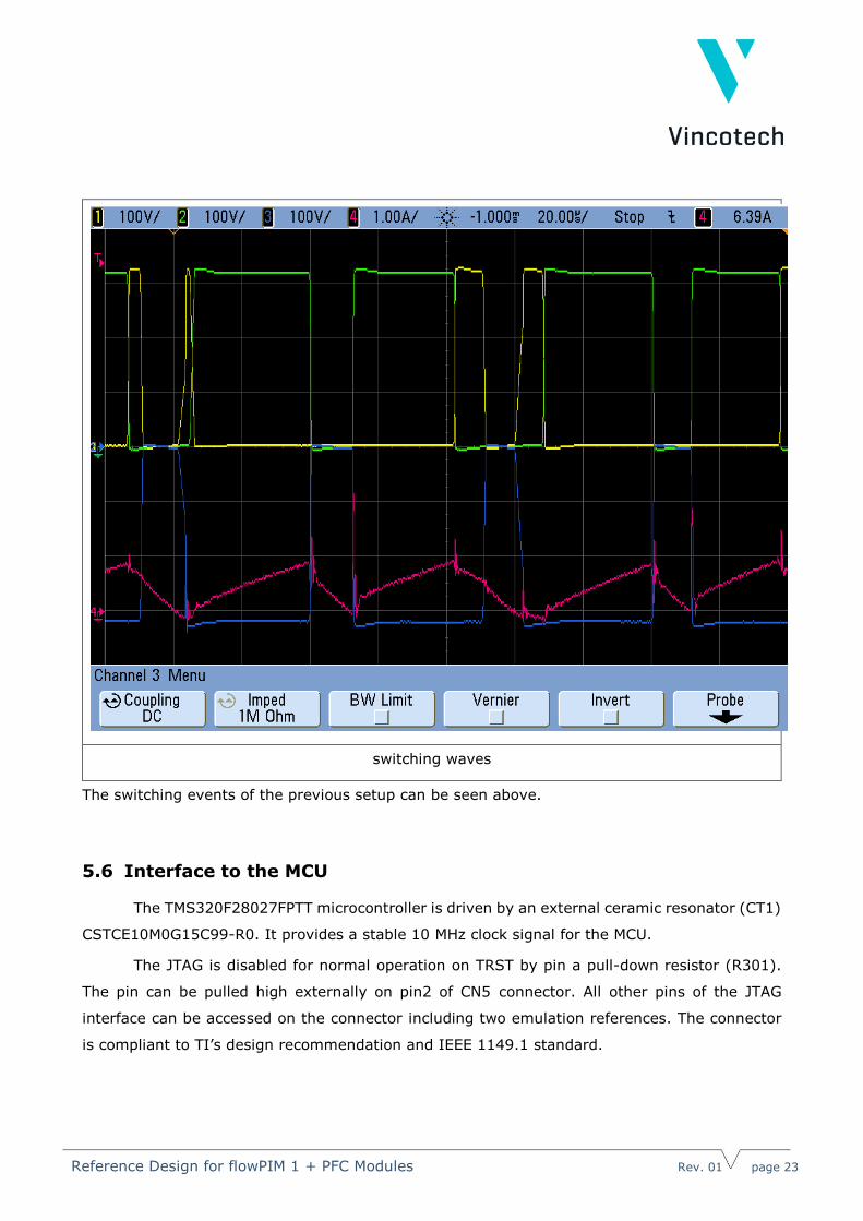
switching waves
The switching events of the previous setup can be seen above.
5.6 Interface to the MCU
The TMS320F28027FPTT microcontroller is driven by an external ceramic resonator (CT1)
CSTCE10M0G15C99-R0. It provides a stable 10 MHz clock signal for the MCU.
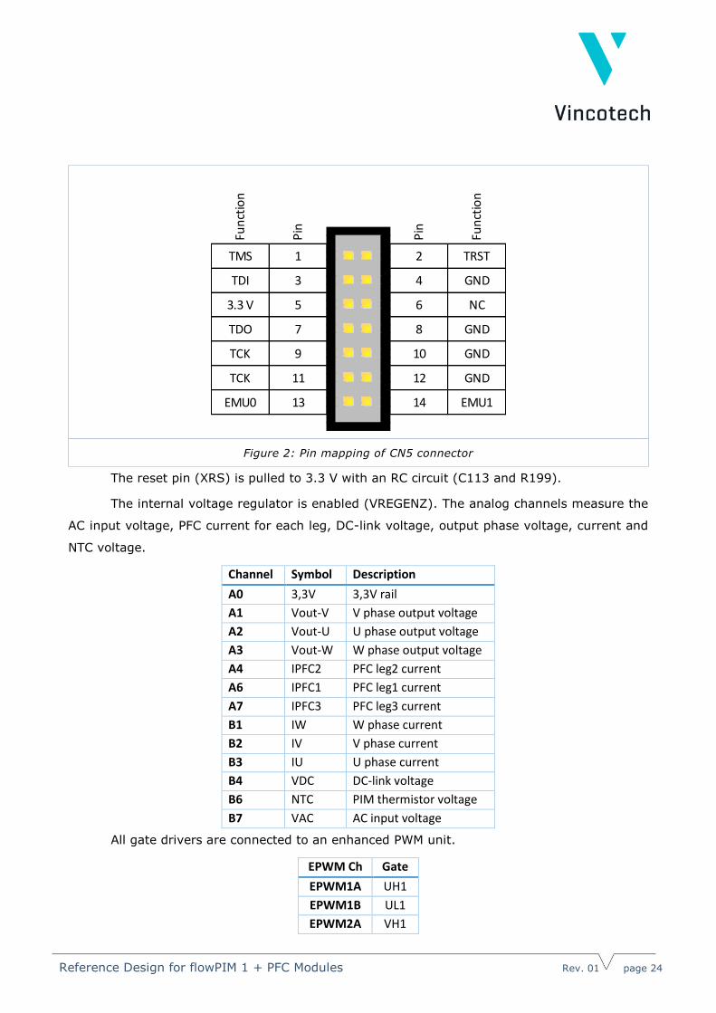
The JTAG is disabled for normal operation on TRST by pin a pull-down resistor (R301).
The pin can be pulled high externally on pin2 of CN5 connector. All other pins of the JTAG
interface can be accessed on the connector including two emulation references. The connector
is compliant to TI’s design recommendation and IEEE 1149.1 standard.
Reference Design for flowPIM 1 + PFC Modules Rev. 01 page 24
Figure 2: Pin mapping of CN5 connector
The reset pin (XRS) is pulled to 3.3 V with an RC circuit (C113 and R199).
The internal voltage regulator is enabled (VREGENZ). The analog channels measure the
AC input voltage, PFC current for each leg, DC-link voltage, output phase voltage, current and
NTC voltage.
Channel Symbol Description
A0 3,3V 3,3V rail
A1 Vout-V V phase output voltage
A2 Vout-U U phase output voltage
A3 Vout-W W phase output voltage
A4 IPFC2 PFC leg2 current
A6 IPFC1 PFC leg1 current
A7 IPFC3 PFC leg3 current
B1 IW W phase current
B2 IV V phase current
B3 IU U phase current
B4 VDC DC-link voltage
B6 NTC PIM thermistor voltage
B7 VAC AC input voltage
All gate drivers are connected to an enhanced PWM unit.
EPWM Ch Gate
EPWM1A UH1
EPWM1B UL1
EPWM2A VH1
b b b b b b bb g g g g g bb g g g g g bb g g g bb g g g g g bb g g g g g bb g g g bb g g g g g bb g g g g g bb g g g bb g g g g g bb g g g g g bb g g g bb g g g g g bb g g g g g bb g g g bb g g g g g bb g g g g g bb g g g bb g g g g g bb g g g g g bb g g g bb g g g g g bb g g g g g bb b b b b b b
Fun
ctio
n
Pin
Pin
Fun
ctio
n
12 GND
14 EMU1
8 GND
10 GND
GND
6 NC
4
2 TRST
EMU0
TMS
TDI
3.3 V
TDO
TCK
TCK
13
1
3
5
7
9
11
Reference Design for flowPIM 1 + PFC Modules Rev. 01 page 25
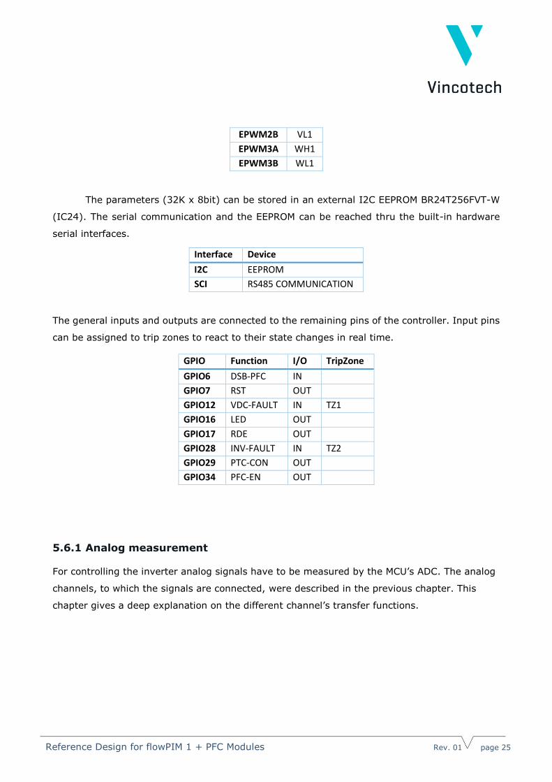
EPWM2B VL1
EPWM3A WH1
EPWM3B WL1
The parameters (32K x 8bit) can be stored in an external I2C EEPROM BR24T256FVT-W
(IC24). The serial communication and the EEPROM can be reached thru the built-in hardware
serial interfaces.
Interface Device
I2C EEPROM
SCI RS485 COMMUNICATION
The general inputs and outputs are connected to the remaining pins of the controller. Input pins
can be assigned to trip zones to react to their state changes in real time.
GPIO Function I/O TripZone
GPIO6 DSB-PFC IN
GPIO7 RST OUT
GPIO12 VDC-FAULT IN TZ1
GPIO16 LED OUT
GPIO17 RDE OUT
GPIO28 INV-FAULT IN TZ2
GPIO29 PTC-CON OUT
GPIO34 PFC-EN OUT
5.6.1 Analog measurement
For controlling the inverter analog signals have to be measured by the MCU’s ADC. The analog
channels, to which the signals are connected, were described in the previous chapter. This
chapter gives a deep explanation on the different channel’s transfer functions.
Reference Design for flowPIM 1 + PFC Modules Rev. 01 page 26
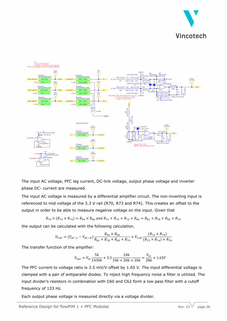
The input AC voltage, PFC leg current, DC-link voltage, output phase voltage and inverter
phase DC- current are measured.
The input AC voltage is measured by a differential amplifier circuit. The non-inverting input is
referenced to mid voltage of the 3.3 V rail (R70, R73 and R74). This creates an offset to the
output in order to be able to measure negative voltage on the input. Given that
𝑅70 × (𝑅73 × 𝑅74) = 𝑅84 × 𝑅86 𝑎𝑛𝑑 𝑅71 + 𝑅75 + 𝑅72 + 𝑅83 = 𝑅81 + 𝑅78 + 𝑅82 + 𝑅79
the output can be calculated with the following calculation.
𝑉𝑉𝐴𝐶 = (𝑉𝐴𝐶−𝐿 − 𝑉𝐴𝐶−𝑁)𝑅84 × 𝑅86
𝑅81 + 𝑅78 + 𝑅82 + 𝑅79
+ 𝑉3.3𝑉
(𝑅73 × 𝑅74)
(𝑅73 × 𝑅74) + 𝑅70
The transfer function of the amplifier:
𝑉𝑜𝑢𝑡 = 𝑉𝑖𝑛
5𝑘
1430𝑘+ 3.3
10𝑘
10𝑘 + 20𝑘 × 20𝑘=
𝑉𝑖𝑛
286+ 1.65𝑉
The PFC current to voltage ratio is 3.5 mV/V offset by 1.65 V. The input differential voltage is
clamped with a pair of antiparallel diodes. To reject high frequency noise a filter is utilized. The
input divider’s resistors in combination with C60 and C62 form a low pass filter with a cutoff
frequency of 133 Hz.
Each output phase voltage is measured directly via a voltage divider.
DCN
3
21
411
IC19ATLV4316IPWR
C77100nF/10%/25V/0603
GND-FB
3.3V-FB
GND-FB
GND-FB
1
TP12IPFC1
DCN
PFC Current sampling, software for unbalance detection1A-CMS=1A*0.005Ω*10+1.65V mid-pointTransfer 1A-CMS=50mV
DCN
1
TP13IPFC2
1
TP14IPFC3
SH
SH-
OUT
DesignatorPfcCurrentMeas.schdoc
β=5
SH
SH-
OUT
Ix-CMP
DesignatorInvCurrentMeas.schdoc
SH
SH-
OUT
DesignatorPfcCurrentMeas.schdoc
SH
SH-
OUT
DesignatorPfcCurrentMeas.schdoc
1
TP22IU
DCN
SH
SH-
OUT
Ix-CMP
DesignatorInvCurrentMeas.schdoc
SH
SH-
OUT
Ix-CMP
DesignatorInvCurrentMeas.schdoc
DCN
DCN
1
TP23IV
1
TP24IW
VDC
VAC
IU
IV
IW
DC
P
IU-SHUNT
IV-SHUNT
IW-SHUNT
PFC1-SHUNT
PFC2-SHUNT
PFC3-SHUNT
IPFC1
IPFC2
IPFC3
1
TP15VOUT-U
1
TP16VOUT-V
1
TP17VOUT-W
IN OUT
DesignatorOutputDevider.schDoc
IN OUT
DesignatorOutputDevider.schDoc
IN OUT
DesignatorOutputDevider.schDoc
Voltage Measurement
VOUT-U
VOUT-V
VOUT-W
U
V
W
R71
470k/1%/1206 R75
470k/1%/1206 R72
470k/1%/1206
C67100pF/10%/25V/0603
R81
470k/1%/1206 R78
470k/1%/1206 R82
470k/1%/1206
C601nF/10%/25V/0603
GND-FB
C621nF/10%/25V/0603
GND-FB
R83
20k/1%/0603
R79
20k/1%/0603
R86 10k/1%/0603
C64 100pF/10%/25V/0603
R80
2K/1%/0603
C63
100pF/10%/25V/0603
R85
1M
/1%
/06
03
GND-FB
R7420k/1%/0603
R7320k/1%/0603
R7010k/1%/0603
3.3V-FB
GND-FB
R84 10k/1%/0603
D18L1SS355T1G
D19L1SS355T1G
5
67
IC11BTLV2316IPWR
1
TP26Test Point
GND-FB
3
21
84
IC11ATLV2316IPWR
GND-FB
C65
100nF/10%/25V/0603GND-FB3.3V-FB
R67
470k
/1%
/120
6
R2
43
47
0k
/1%
/1206
R6
8470
k/1
%/1
206
R69
20k/1
%/0
603
R255
20k/1
%/0
603
GND-FB
C1
46
100pF/10%/25V/0603
D21 L1SS355T1G
12
1314
IC15DTLV4316IPWR
R252
2K/1%/0603
C1
49
100pF/10%/25V/0603
R25
6
1M
/1%
/06
03
GND-FB
3.3V-FB 1
TP25Test Point
380VDC=380*10K/1420K=2.676VTransfer 1VDC=7mV
β=5/1430 Cutoff frequency=113Hz220V-RMS=220*1.414*5/1430±1.65V mid-point
Transfer 1V-CMS=3.5mV
IU-C
MP
IV-.
CM
PIW
-CM
P
Ix-CMP
Ix-CMP
AC-L
AC-N
Reference Design for flowPIM 1 + PFC Modules Rev. 01 page 27
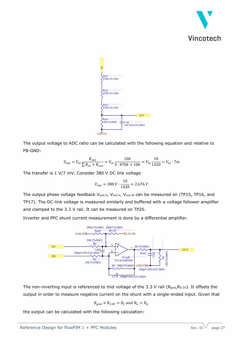
The output voltage to ADC ratio can be calculated with the following equation and relative to
FB-GND:
𝑉𝑜𝑢𝑡 = 𝑉𝑖𝑛
𝑅𝑜𝑢𝑡
∑ 𝑅𝑖𝑛 + 𝑅𝑜𝑢𝑡
= 𝑉𝑖𝑛
10𝑘
3 ∙ 470𝑘 + 10𝑘= 𝑉𝑖𝑛
10
1420= 𝑉𝑖𝑛 ∙ 7𝑚
The transfer is 1 V/7 mV. Consider 380 V DC link voltage
𝑉𝑜𝑢𝑡 = 380 𝑉 ∙10
1420= 2.676 𝑉
The output phase voltage feedback Vout-U, Vout-V, Vout-W can be measured on (TP15, TP16, and
TP17). The DC-link voltage is measured similarly and buffered with a voltage follower amplifier
and clamped to the 3.3 V rail. It can be measured on TP25.
Inverter and PFC shunt current measurement is done by a differential amplifier.
The non-inverting input is referenced to mid voltage of the 3.3 V rail (Rgnd,R3.3V). It offsets the
output in order to measure negative current on the shunt with a single-ended input. Given that
𝑅𝑔𝑛𝑑 × 𝑅3.3𝑉 = 𝑅𝑓 𝑎𝑛𝑑 𝑅𝑛 = 𝑅𝑝
the output can be calculated with the following calculation:
IN
OUT
Rin1 (Rin1_Designator14, ...)
470k/1%/1206
Rin2 (Rin2_Designator14, ...)
470k/1%/1206
Rin3 (Rin3_Designator14, ...)
470k/1%/1206
Rout (Rout_Designator14, ...)
10k/1%/0603
380VDC=380*10K/1420K=2.676VTransfer 1VDC=7mV
GND-FB
Cout (Cout_Designator14, ...)
1nF/10%/25V/0603
SH
SH-
OUT
Rf (Rf_Designator18, ...)100k/1%/0603
Rp (Rp_Designator18, ...)
10k/1%/0603
Rgnd (Rgnd_Designator18, ...)
200k/1%/0603
Rn (Rn_Designator18, ...)
10k/1%/0603
Cdiff (Cdiff_Designator18, ...)
100pF/10%/25V/0603
Cf (Cf_Designator18, ...)100pF/10%/25V/0603
R3.3V (R3.3V_Designator18, ...)
200k/1%/0603
GND-FB
Rout (Rout_Designator18, ...)
2K/1%/0603
Cout
(Co
ut_
Des
ign
ato
r18
, ..
.)
100pF/10%/25V/0603
Rz
(Rz_
Des
ign
ato
r18
, ..
.)
1M
/1%
/0603
GND-FB
5
67
ICoaB (ICoa_Designator18B, ...)
TLV4316IPWR
3.3V-FB
PFC Current sampling, software for unbalance detection1A-CMS=1A*0.005Ω*10+1.65V mid-pointTransfer 1A-CMS=50mV
Reference Design for flowPIM 1 + PFC Modules Rev. 01 page 28
𝑉𝑜𝑢𝑡 = (𝑉𝑆𝐻 − 𝑉𝑆𝐻−)𝑅𝑓
𝑅𝑛
+ 𝑉3.3𝑉
𝑅𝑔𝑛𝑑
𝑅𝑔𝑛𝑑 + 𝑅3.3𝑉
The voltage drop on the shunt is:
𝑉𝑠ℎ𝑢𝑛𝑡 = 𝑅𝑠ℎ𝑢𝑛𝑡 ∙ 𝐼 = 0.005Ω ∙ 𝐼
Finally, the transfer function of the amplifier (PFC):
𝑉𝑜𝑢𝑡 = (0.005 ∙ 𝐼)10𝑘
100𝑘+ 3.3
200𝑘
200𝑘 + 200𝑘= 0.05𝐼 + 1.65𝑉
The PFC current to voltage ratio is 50 mV/A offset by 1.65 V The Inverter current to voltage
ratio is 25 mV/A offset by 1.65 V.
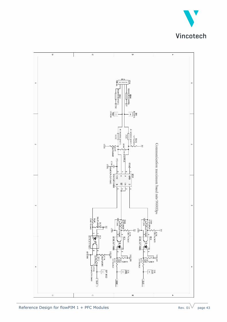
5.6.2 Communication
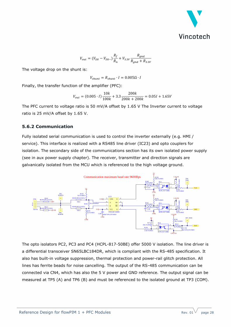
Fully isolated serial communication is used to control the inverter externally (e.g. HMI /
service). This interface is realized with a RS485 line driver (IC23) and opto couplers for
isolation. The secondary side of the communications section has its own isolated power supply
(see in aux power supply chapter). The receiver, transmitter and direction signals are
galvanically isolated from the MCU which is referenced to the high voltage ground.
The opto isolators PC2, PC3 and PC4 (HCPL-817-50BE) offer 5000 V isolation. The line driver is
a differential transceiver SN65LBC184DR, which is compliant with the RS-485 specification. It
also has built-in voltage suppression, thermal protection and power-rail glitch protection. All
lines has ferrite beads for noise cancelling. The output of the RS-485 communication can be
connected via CN4, which has also the 5 V power and GND reference. The output signal can be
measured at TP5 (A) and TP6 (B) and must be referenced to the isolated ground at TP3 (COM).
1
2
4
3
PC4
HCPL-817-50BE
R172
10k/1%/0603
R149
3.3k/1%/0603
5VR14610k/1%/0603
3.3V-FB
R213
1k/1%/0603C156
1nF/10%/25V/0603
GND-FB
1
TP7 RXD
TxD
DRE
RxD
5V
R1561k/1%/0603
R1951k/1%/0603
COM
R194 Not assembled
R1
RE2
DE3
D4
GND5
B7
VCC8
A6
IC23
SN65LBC184DR
5V
C108100nF/10%/25V/0603
COM
COM
FB13
BLM31PG121SZ1L
FB11
BLM31PG121SZ1L
1234
CN4
XH-4A
FB10BLM31PG121SZ1L
5VA
B
FB12BLM31PG121SZ1L
COM
1
TP5RS485A
1
TP6RS485B
1
2
4
3
PC2
HCPL-817-50BE
R1
42
10k/1
%/0
60
3
R1441k/1%/0603
3.3V-FBR13810k/1%/0603
5V
R1401k/1%/0603
C1541nF/10%/25V/0603
COM
1
TP8TXD
1
2
4
3
PC3
HCPL-817-50BE
R143
10k/1
%/0
60
3
R1451k/1%/0603
3.3V-FBR13910k/1%/0603
5V
R1411k/1%/0603
C1481nF/10%/25V/0603
COM
1
TP9DRE
Communication maximum baud rate 9600Bps
Reference Design for flowPIM 1 + PFC Modules Rev. 01 page 29
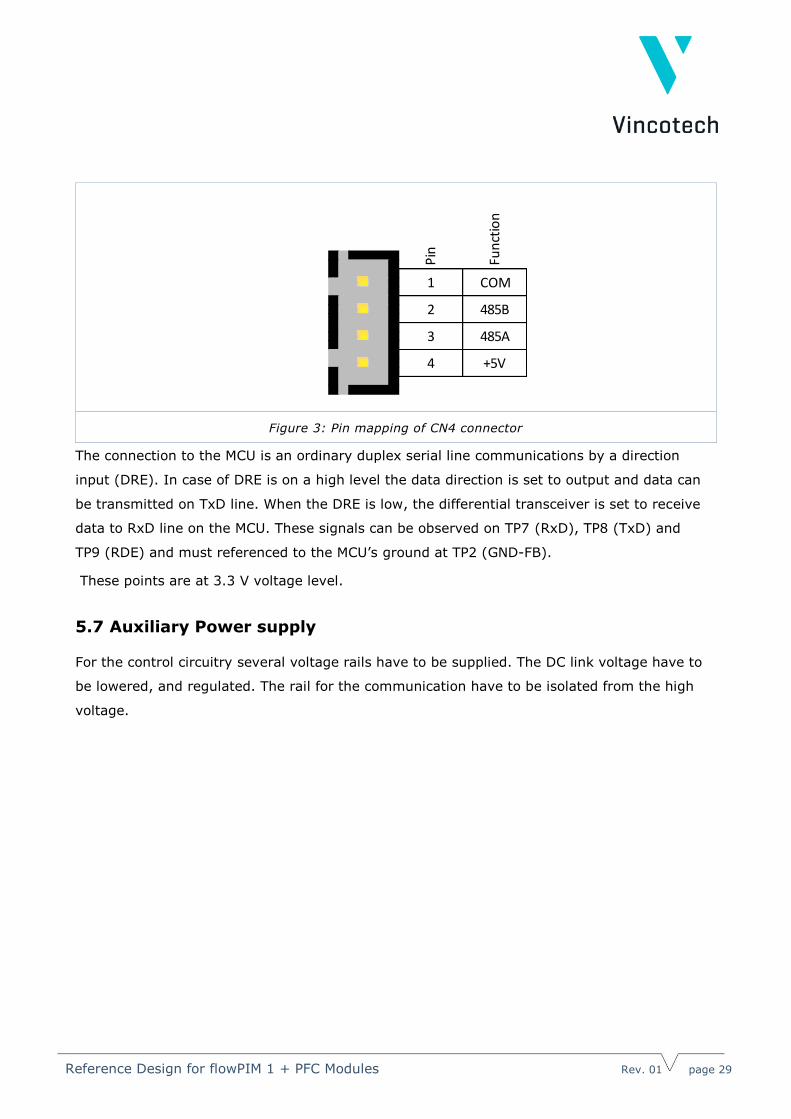
Figure 3: Pin mapping of CN4 connector
The connection to the MCU is an ordinary duplex serial line communications by a direction
input (DRE). In case of DRE is on a high level the data direction is set to output and data can
be transmitted on TxD line. When the DRE is low, the differential transceiver is set to receive
data to RxD line on the MCU. These signals can be observed on TP7 (RxD), TP8 (TxD) and
TP9 (RDE) and must referenced to the MCU’s ground at TP2 (GND-FB).
These points are at 3.3 V voltage level.
5.7 Auxiliary Power supply
For the control circuitry several voltage rails have to be supplied. The DC link voltage have to
be lowered, and regulated. The rail for the communication have to be isolated from the high
voltage.
b g b b b b bb g g g g g bb g g g g g bg g g g g bg g g g g g bb g g g g g bb g g g g bb g g g g g bb g g g g g bb g g g g bb g g g g g bg g g g g g bg g g g g bb g g g g g bb g g g g g bb g b b b b b
4 +5V
2 485B
3 485A
Pin
Fun
ctio
n
1 COM
Reference Design for flowPIM 1 + PFC Modules Rev. 01 page 30
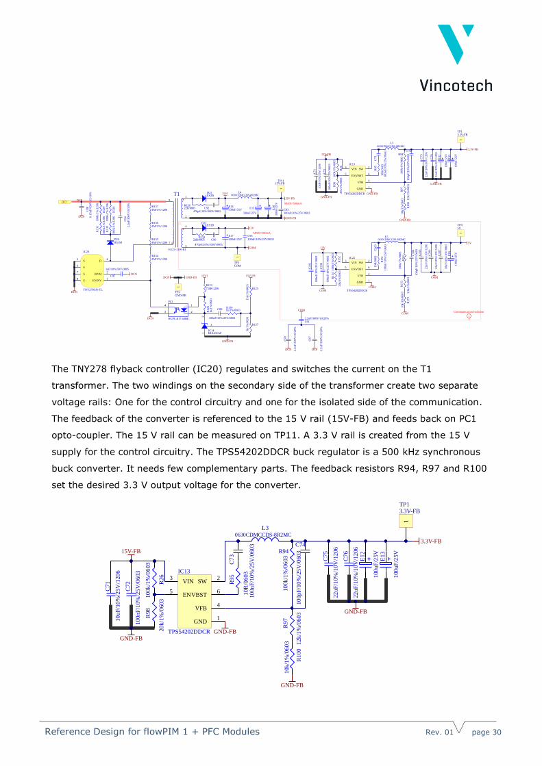
The TNY278 flyback controller (IC20) regulates and switches the current on the T1
transformer. The two windings on the secondary side of the transformer create two separate
voltage rails: One for the control circuitry and one for the isolated side of the communication.
The feedback of the converter is referenced to the 15 V rail (15V-FB) and feeds back on PC1
opto-coupler. The 15 V rail can be measured on TP11. A 3.3 V rail is created from the 15 V
supply for the control circuitry. The TPS54202DDCR buck regulator is a 500 kHz synchronous
buck converter. It needs few complementary parts. The feedback resistors R94, R97 and R100
set the desired 3.3 V output voltage for the converter.
C88
0.1
5u
F/6
30
V/1
5/1
0%
DCN
C9
0
2.2
nF
/300
V/1
0/2
0%
C912.2nF/300V/10/20%
C8
7
2.2
nF
/300
V/1
0/2
0%
DCPDCN
COM
R125
15
k/1
%/0
60
3
R127
3k/1
%/0
60
3
1
2
4
3
PC1
HCPL-817-50BE
R123750R/1206
R1
26
1k
/1%
/0603
15V1
DCN
12
3
IC14KIA431AF
GND-FB
15V-FB
R1241k/1%/0603C89
100nF/10%/25V/0603
EN/NV1
BP/M2
D4
S5
S6
S7
S8
IC20
TNY278GN-TL
C97
1uF/10%/50V/0805
R1341M/1%/1206
R1351M/1%/1206
R1361M/1%/1206
R1371M/1%/1206
D24HS1M
D22ES2B
D23ES1B
R13
1
100
K/1
%/1
206
R13
2
100
K/1
%/1
206
R12
9
10
0K
/1%
/1206
R13
0
10
0K
/1%
/1206
7
9
*
1*
2
4*
5
T1
EE25-13W-RI
C92470pF/10%/100V/0805
R12822R/0805
E14330uF/25V
L40630CDMCCDS-8R2MC
E15
330uF/25V
E1
633
0uF
/25V
C93100nF/10%/25V/0603
GND-FB
15V-FB
15V1
C96
470pF/10%/100V/0805
R13322R/0805
C95100nF/10%/25V/0603
COM
12V
MAX=200mA
MAX=500mA
C94
2.2
nF
/300
V/1
0/2
0%
E17100uF/25V
1
TP1115V-FB
SW2
VIN3
VFB4
EN5
VBST6
GND1
IC13
TPS54202DDCR
L30630CDMCCDS-8R2MC
R95
10R
/06
03
C7
3
10
0n
F/1
0%
/25V
/06
03
C7
5
22
uF
/10%
/10
V/1
20
6
C7
6
22
uF
/10%
/10
V/1
20
6
R94
10
0k/1
%/0
603
R97
12
k/1
%/0
60
3R
100
10k/1
%/0
603
GND-FB
C74
10
0p
F/1
0%
/25V
/0603
R26
10
0k
/1%
/06
03
R98
20
k/1
%/0
60
3
C71
100
nF
/10%
/25
V/0
60
3
C72
10u
F/1
0%
/25V
/1206
GND-FB
E13
100
uF
/25V
GND-FB
3.3V-FB
E12
100
uF
/25V
DC+
1
TP13.3V-FB
1
TP2GND-FB
1
TP3COM
GND-FB
15V-FB
GND-FB
DCN
DCNDCN
SW2
VIN3
VFB4
EN5
VBST6
GND1
IC22
TPS54202DDCR
L50630CDMCCDS-8R2MC
R1
51
10R
/060
3C
10
3
100
nF
/10%
/25
V/0
60
3
C15
3
22u
F/1
0%
/10V
/12
06
C10
6
22u
F/1
0%
/10V
/12
06
COM
R2
111
00
k/1
%/0
60
3R
153
3.3
k/1
%/0
603
R1
73
10k
/1%
/060
3
COM
C10
410
0pF
/10%
/25V
/06
03
5V
12V
R1
52
100
k/1
%/0
60
3R
154
20k
/1%
/0603
COM
C101
10
0n
F/1
0%
/25V
/0603
1
TP45V
COM
C10
7
10u
F/1
0%
/16V
/08
05
E1
8
100u
F/2
5V
i
Communication Isolation
C150
10
0n
F/1
0%
/25V
/0603
DCP
Reference Design for flowPIM 1 + PFC Modules Rev. 01 page 31
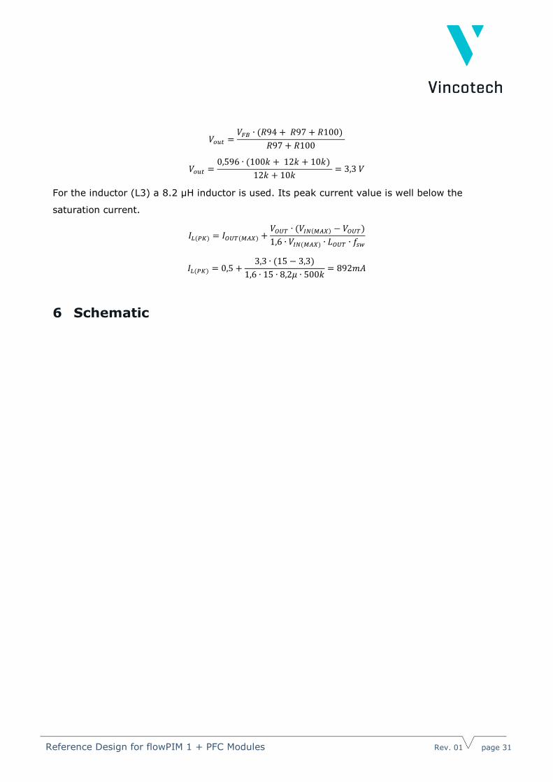
𝑉𝑜𝑢𝑡 =𝑉𝐹𝐵 ∙ (𝑅94 + 𝑅97 + 𝑅100)
𝑅97 + 𝑅100
𝑉𝑜𝑢𝑡 =0,596 ∙ (100𝑘 + 12𝑘 + 10𝑘)
12𝑘 + 10𝑘= 3,3 𝑉
For the inductor (L3) a 8.2 µH inductor is used. Its peak current value is well below the
saturation current.
𝐼𝐿(𝑃𝐾) = 𝐼𝑂𝑈𝑇(𝑀𝐴𝑋) +𝑉𝑂𝑈𝑇 ∙ (𝑉𝐼𝑁(𝑀𝐴𝑋) − 𝑉𝑂𝑈𝑇)
1,6 ∙ 𝑉𝐼𝑁(𝑀𝐴𝑋) ∙ 𝐿𝑂𝑈𝑇 ∙ 𝑓𝑠𝑤
𝐼𝐿(𝑃𝐾) = 0,5 +3,3 ∙ (15 − 3,3)
1,6 ∙ 15 ∙ 8,2𝜇 ∙ 500𝑘= 892𝑚𝐴
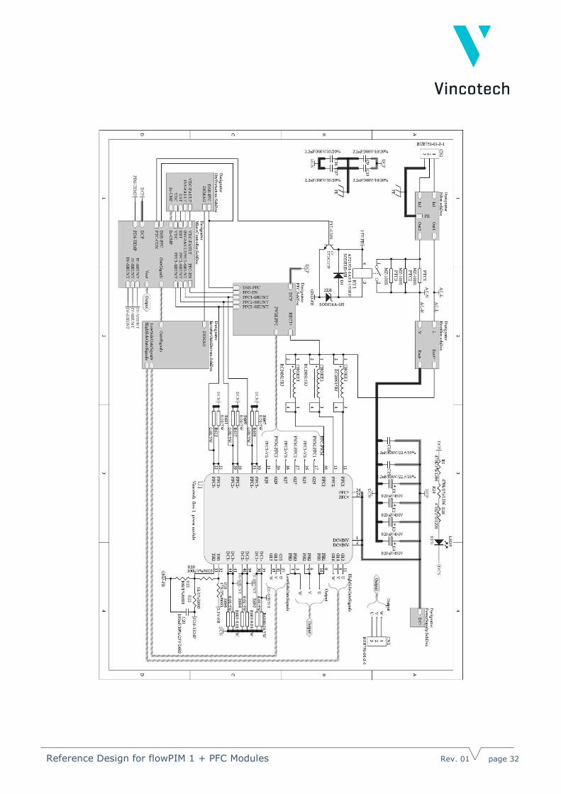
6 Schematic
Reference Design for flowPIM 1 + PFC Modules Rev. 01 page 32
Reference Design for flowPIM 1 + PFC Modules Rev. 01 page 33
Reference Design for flowPIM 1 + PFC Modules Rev. 01 page 34
Reference Design for flowPIM 1 + PFC Modules Rev. 01 page 35
Reference Design for flowPIM 1 + PFC Modules Rev. 01 page 36
Reference Design for flowPIM 1 + PFC Modules Rev. 01 page 37
Reference Design for flowPIM 1 + PFC Modules Rev. 01 page 38
Reference Design for flowPIM 1 + PFC Modules Rev. 01 page 39
Reference Design for flowPIM 1 + PFC Modules Rev. 01 page 40
Reference Design for flowPIM 1 + PFC Modules Rev. 01 page 41
Reference Design for flowPIM 1 + PFC Modules Rev. 01 page 42
Reference Design for flowPIM 1 + PFC Modules Rev. 01 page 43
Reference Design for flowPIM 1 + PFC Modules Rev. 01 page 44
Reference Design for flowPIM 1 + PFC Modules Rev. 01 page 45
Reference Design for flowPIM 1 + PFC Modules Rev. 01 page 46
Reference Design for flowPIM 1 + PFC Modules Rev. 01 page 47
Reference Design for flowPIM 1 + PFC Modules Rev. 01 page 48
Reference Design for flowPIM 1 + PFC Modules Rev. 01 page 49
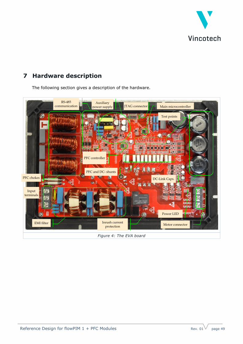
7 Hardware description
The following section gives a description of the hardware.
Figure 4: The EVA board
PFC and DC- shunts
RS-485 communication
PFC controller
Main microcontroller
EMI filter Motor connector
Auxiliary power supply
adjust
Test points
PFC chokes
Inrush current protection
Power LED
DC-Link Caps.
JTAG connector
Input terminals
Reference Design for flowPIM 1 + PFC Modules Rev. 01 page 50
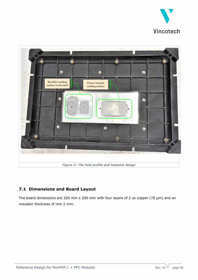
Figure 5: The hole profile and heatsink design
7.1 Dimensions and Board Layout
The board dimensions are 320 mm x 200 mm with four layers of 2 oz copper (70 µm) and an
insulator thickness of min 2 mm.
Rectifier cooling surface is elevated
Power module cooling surface
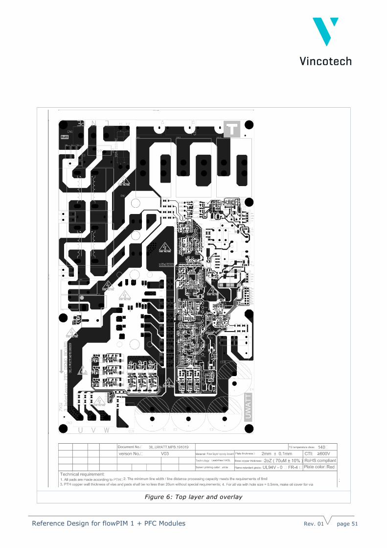
Reference Design for flowPIM 1 + PFC Modules Rev. 01 page 51
Figure 6: Top layer and overlay
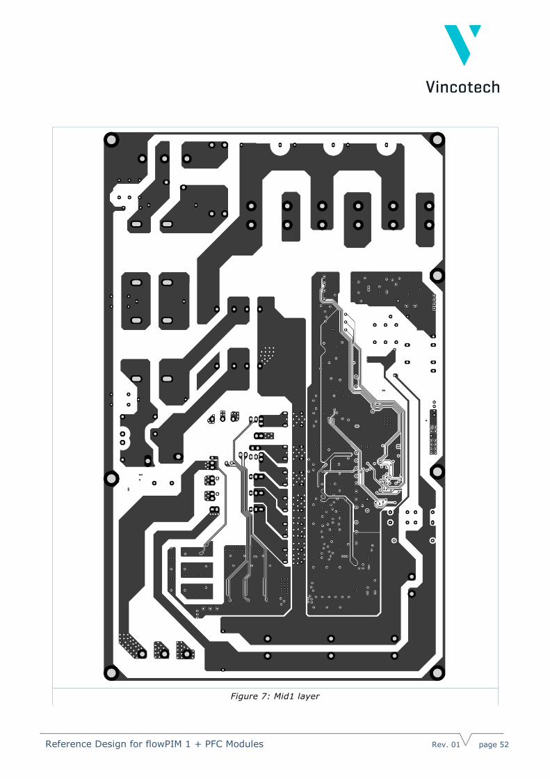
Reference Design for flowPIM 1 + PFC Modules Rev. 01 page 52
Figure 7: Mid1 layer
Reference Design for flowPIM 1 + PFC Modules Rev. 01 page 53
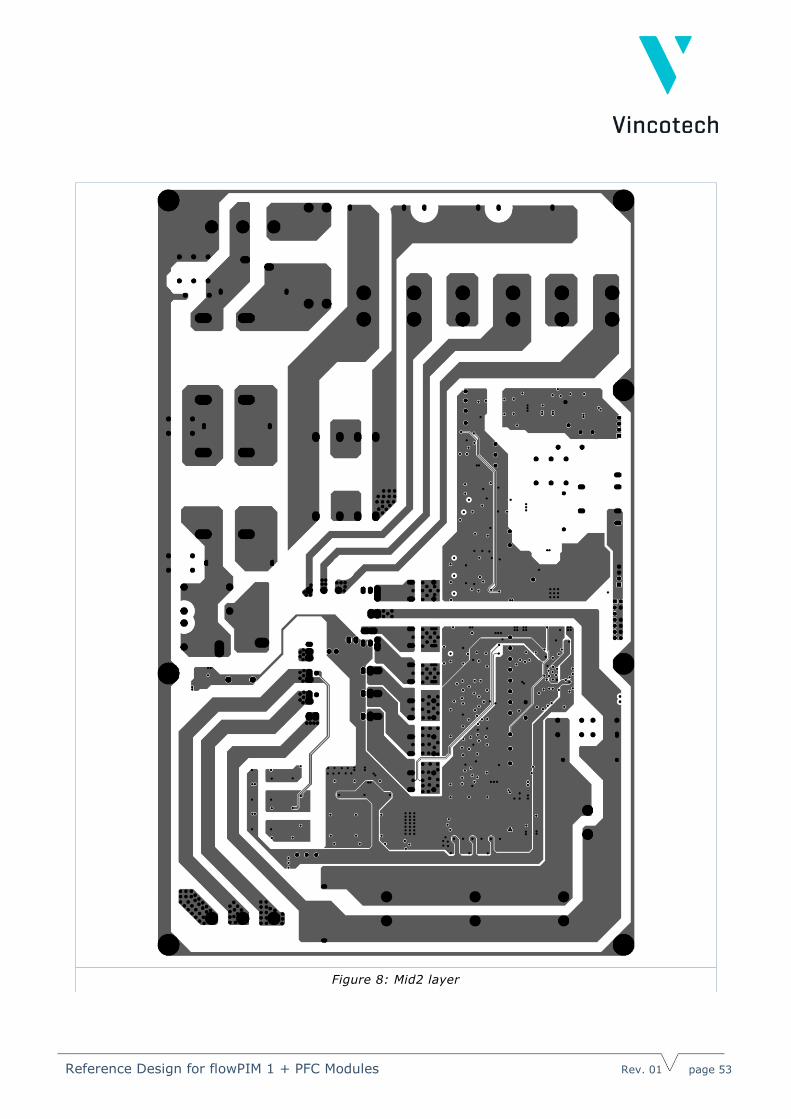
Figure 8: Mid2 layer
Reference Design for flowPIM 1 + PFC Modules Rev. 01 page 54
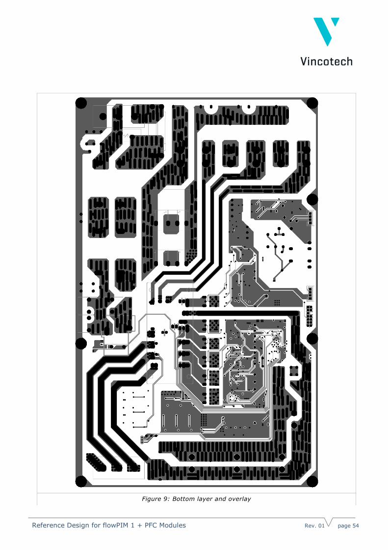
Figure 9: Bottom layer and overlay
Reference Design for flowPIM 1 + PFC Modules Rev. 01 page 55
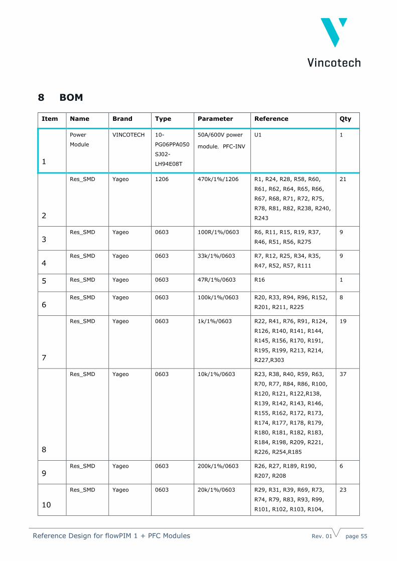
8 BOM
Item Name Brand Type Parameter Reference Qty
1
Power
Module
VINCOTECH 10-
PG06PPA050
SJ02-
LH94E08T
50A/600V power
module,PFC-INV
U1 1
2
Res_SMD Yageo 1206 470k/1%/1206 R1, R24, R28, R58, R60,
R61, R62, R64, R65, R66,
R67, R68, R71, R72, R75,
R78, R81, R82, R238, R240,
R243
21
3 Res_SMD Yageo 0603 100R/1%/0603 R6, R11, R15, R19, R37,
R46, R51, R56, R275
9
4 Res_SMD Yageo 0603 33k/1%/0603 R7, R12, R25, R34, R35,
R47, R52, R57, R111
9
5 Res_SMD Yageo 0603 47R/1%/0603 R16 1
6 Res_SMD Yageo 0603 100k/1%/0603 R20, R33, R94, R96, R152,
R201, R211, R225
8
7
Res_SMD Yageo 0603 1k/1%/0603 R22, R41, R76, R91, R124,
R126, R140, R141, R144,
R145, R156, R170, R191,
R195, R199, R213, R214,
R227,R303
19
8
Res_SMD Yageo 0603 10k/1%/0603 R23, R38, R40, R59, R63,
R70, R77, R84, R86, R100,
R120, R121, R122,R138,
R139, R142, R143, R146,
R155, R162, R172, R173,
R174, R177, R178, R179,
R180, R181, R182, R183,
R184, R198, R209, R221,
R226, R254,R185
37
9 Res_SMD Yageo 0603 200k/1%/0603 R26, R27, R189, R190,
R207, R208
6
10
Res_SMD Yageo 0603 20k/1%/0603 R29, R31, R39, R69, R73,
R74, R79, R83, R93, R99,
R101, R102, R103, R104,
23
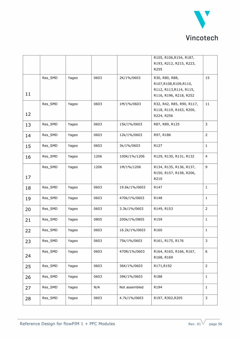
Reference Design for flowPIM 1 + PFC Modules Rev. 01 page 56
R105, R106,R154, R187,
R193, R212, R215, R223,
R255
11
Res_SMD Yageo 0603 2K/1%/0603 R30, R80, R88,
R107,R108,R109,R110,
R112, R113,R114, R115,
R116, R196, R218, R252
15
12
Res_SMD Yageo 0603 1M/1%/0603 R32, R42, R85, R90, R117,
R118, R119, R163, R200,
R224, R256
11
13 Res_SMD Yageo 0603 15k/1%/0603 R87, R89, R125 3
14 Res_SMD Yageo 0603 12k/1%/0603 R97, R186 2
15 Res_SMD Yageo 0603 3k/1%/0603 R127 1
16 Res_SMD Yageo 1206 100K/1%/1206 R129, R130, R131, R132 4
17
Res_SMD Yageo 1206 1M/1%/1206 R134, R135, R136, R137,
R150, R157, R158, R206,
R210
9
18 Res_SMD Yageo 0603 19.6k/1%/0603 R147 1
19 Res_SMD Yageo 0603 470k/1%/0603 R148 1
20 Res_SMD Yageo 0603 3.3k/1%/0603 R149, R153 2
21 Res_SMD Yageo 0805 200k/1%/0805 R159 1
22 Res_SMD Yageo 0603 16.2k/1%/0603 R160 1
23 Res_SMD Yageo 0603 75k/1%/0603 R161, R175, R176 3
24 Res_SMD Yageo 0603 470R/1%/0603 R164, R165, R166, R167,
R168, R169
6
25 Res_SMD Yageo 0603 36K/1%/0603 R171,R192 2
26 Res_SMD Yageo 0603 39K/1%/0603 R188 1
27 Res_SMD Yageo N/A Not assembled R194 1
28 Res_SMD Yageo 0603 4.7k/1%/0603 R197, R302,R205 3
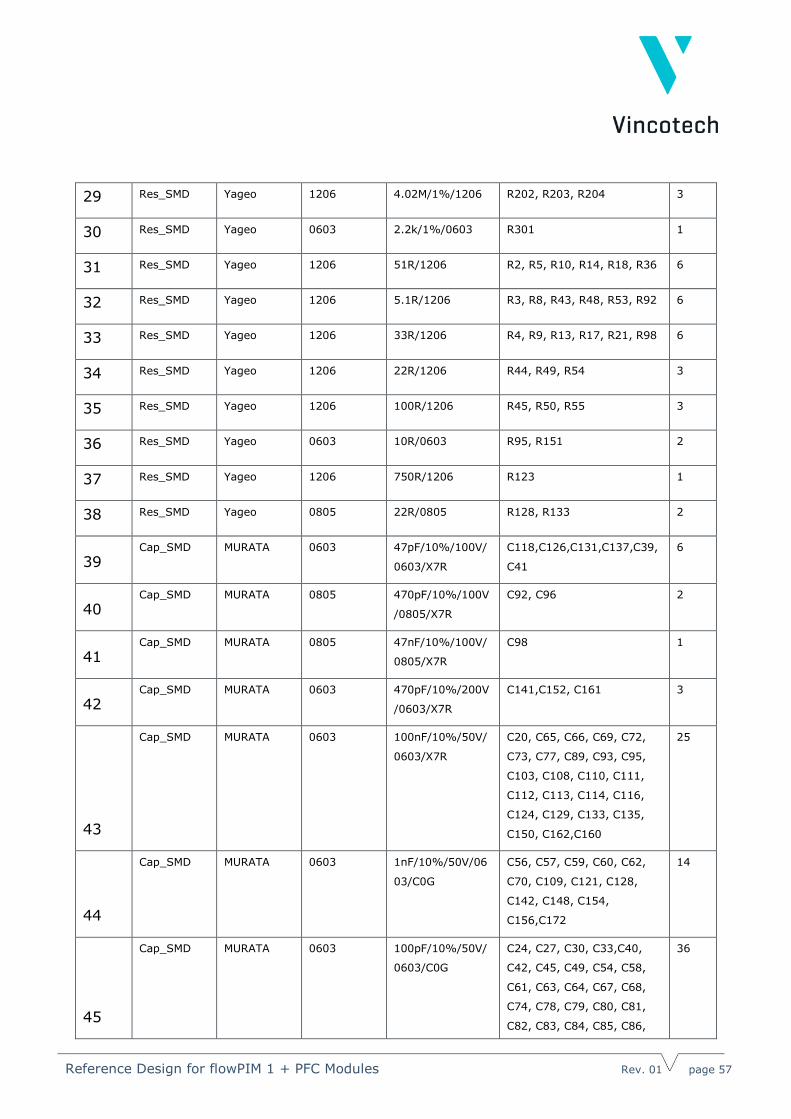
Reference Design for flowPIM 1 + PFC Modules Rev. 01 page 57
29 Res_SMD Yageo 1206 4.02M/1%/1206 R202, R203, R204 3
30 Res_SMD Yageo 0603 2.2k/1%/0603 R301 1
31 Res_SMD Yageo 1206 51R/1206 R2, R5, R10, R14, R18, R36 6
32 Res_SMD Yageo 1206 5.1R/1206 R3, R8, R43, R48, R53, R92 6
33 Res_SMD Yageo 1206 33R/1206 R4, R9, R13, R17, R21, R98 6
34 Res_SMD Yageo 1206 22R/1206 R44, R49, R54 3
35 Res_SMD Yageo 1206 100R/1206 R45, R50, R55 3
36 Res_SMD Yageo 0603 10R/0603 R95, R151 2
37 Res_SMD Yageo 1206 750R/1206 R123 1
38 Res_SMD Yageo 0805 22R/0805 R128, R133 2
39 Cap_SMD MURATA 0603 47pF/10%/100V/
0603/X7R
C118,C126,C131,C137,C39,
C41
6
40 Cap_SMD MURATA 0805 470pF/10%/100V
/0805/X7R
C92, C96 2
41 Cap_SMD MURATA 0805 47nF/10%/100V/
0805/X7R
C98 1
42 Cap_SMD MURATA 0603 470pF/10%/200V
/0603/X7R
C141,C152, C161 3
43
Cap_SMD MURATA 0603 100nF/10%/50V/
0603/X7R
C20, C65, C66, C69, C72,
C73, C77, C89, C93, C95,
C103, C108, C110, C111,
C112, C113, C114, C116,
C124, C129, C133, C135,
C150, C162,C160
25
44
Cap_SMD MURATA 0603 1nF/10%/50V/06
03/C0G
C56, C57, C59, C60, C62,
C70, C109, C121, C128,
C142, C148, C154,
C156,C172
14
45
Cap_SMD MURATA 0603 100pF/10%/50V/
0603/C0G
C24, C27, C30, C33,C40,
C42, C45, C49, C54, C58,
C61, C63, C64, C67, C68,
C74, C78, C79, C80, C81,
C82, C83, C84, C85, C86,
36
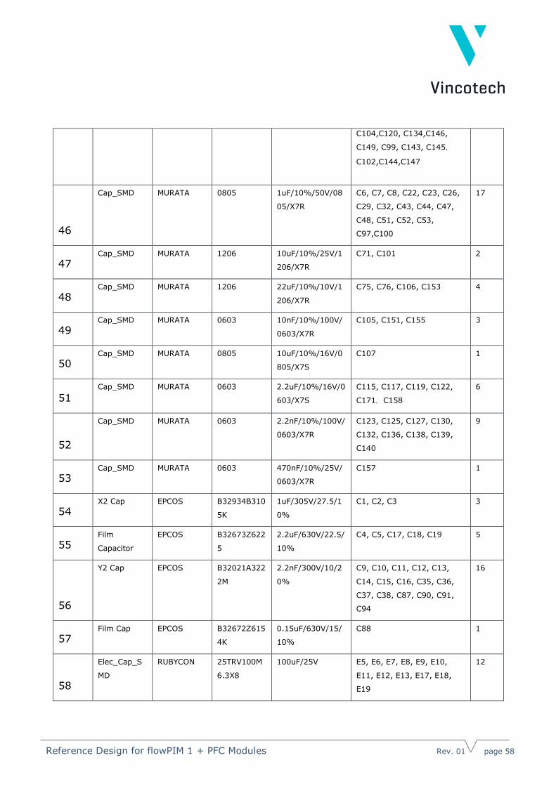
Reference Design for flowPIM 1 + PFC Modules Rev. 01 page 58
C104,C120, C134,C146,
C149, C99, C143, C145,
C102,C144,C147
46
Cap_SMD MURATA 0805 1uF/10%/50V/08
05/X7R
C6, C7, C8, C22, C23, C26,
C29, C32, C43, C44, C47,
C48, C51, C52, C53,
C97,C100
17
47 Cap_SMD MURATA 1206 10uF/10%/25V/1
206/X7R
C71, C101 2
48 Cap_SMD MURATA 1206 22uF/10%/10V/1
206/X7R
C75, C76, C106, C153 4
49 Cap_SMD MURATA 0603 10nF/10%/100V/
0603/X7R
C105, C151, C155 3
50 Cap_SMD MURATA 0805 10uF/10%/16V/0
805/X7S
C107 1
51
Cap_SMD MURATA 0603 2.2uF/10%/16V/0
603/X7S
C115, C117, C119, C122,
C171,C158
6
52
Cap_SMD MURATA 0603 2.2nF/10%/100V/
0603/X7R
C123, C125, C127, C130,
C132, C136, C138, C139,
C140
9
53 Cap_SMD MURATA 0603 470nF/10%/25V/
0603/X7R
C157 1
54 X2 Cap EPCOS B32934B310
5K
1uF/305V/27.5/1
0%
C1, C2, C3 3
55 Film
Capacitor
EPCOS B32673Z622
5
2.2uF/630V/22.5/
10%
C4, C5, C17, C18, C19 5
56
Y2 Cap EPCOS B32021A322
2M
2.2nF/300V/10/2
0%
C9, C10, C11, C12, C13,
C14, C15, C16, C35, C36,
C37, C38, C87, C90, C91,
C94
16
57 Film Cap EPCOS B32672Z615
4K
0.15uF/630V/15/
10%
C88 1
58
Elec_Cap_S
MD
RUBYCON 25TRV100M
6.3X8
100uF/25V E5, E6, E7, E8, E9, E10,
E11, E12, E13, E17, E18,
E19
12
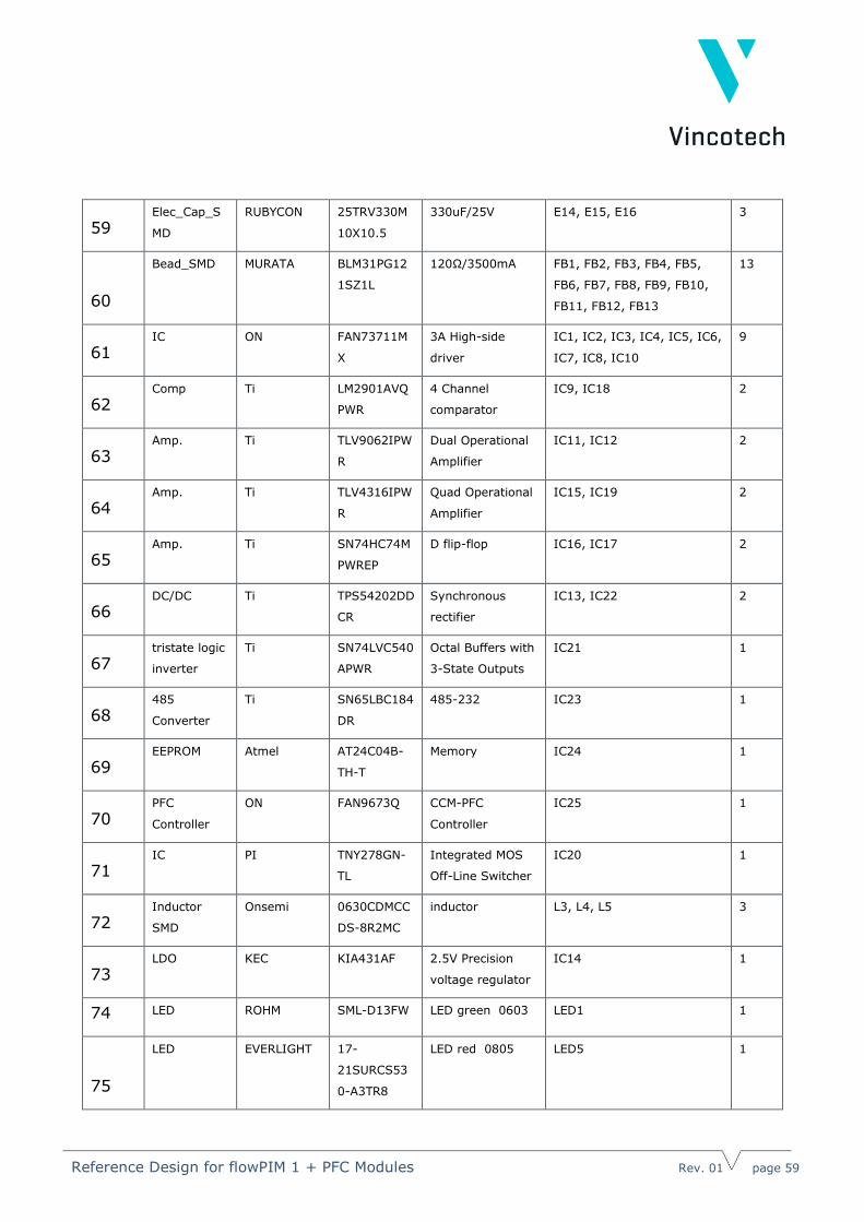
Reference Design for flowPIM 1 + PFC Modules Rev. 01 page 59
59 Elec_Cap_S
MD
RUBYCON 25TRV330M
10X10.5
330uF/25V E14, E15, E16 3
60
Bead_SMD MURATA BLM31PG12
1SZ1L
120Ω/3500mA FB1, FB2, FB3, FB4, FB5,
FB6, FB7, FB8, FB9, FB10,
FB11, FB12, FB13
13
61 IC ON FAN73711M
X
3A High-side
driver
IC1, IC2, IC3, IC4, IC5, IC6,
IC7, IC8, IC10
9
62 Comp Ti LM2901AVQ
PWR
4 Channel
comparator
IC9, IC18 2
63 Amp. Ti TLV9062IPW
R
Dual Operational
Amplifier
IC11, IC12 2
64 Amp. Ti TLV4316IPW
R
Quad Operational
Amplifier
IC15, IC19 2
65 Amp. Ti SN74HC74M
PWREP
D flip-flop IC16, IC17 2
66 DC/DC Ti TPS54202DD
CR
Synchronous
rectifier
IC13, IC22 2
67 tristate logic
inverter
Ti SN74LVC540
APWR
Octal Buffers with
3-State Outputs
IC21 1
68 485
Converter
Ti SN65LBC184
DR
485-232 IC23 1
69 EEPROM Atmel AT24C04B-
TH-T
Memory IC24 1
70 PFC
Controller
ON FAN9673Q CCM-PFC
Controller
IC25 1
71 IC PI TNY278GN-
TL
Integrated MOS
Off-Line Switcher
IC20 1
72 Inductor
SMD
Onsemi 0630CDMCC
DS-8R2MC
inductor L3, L4, L5 3
73 LDO KEC KIA431AF 2.5V Precision
voltage regulator
IC14 1
74 LED ROHM SML-D13FW LED green 0603 LED1 1
75
LED EVERLIGHT 17-
21SURCS53
0-A3TR8
LED red 0805 LED5 1
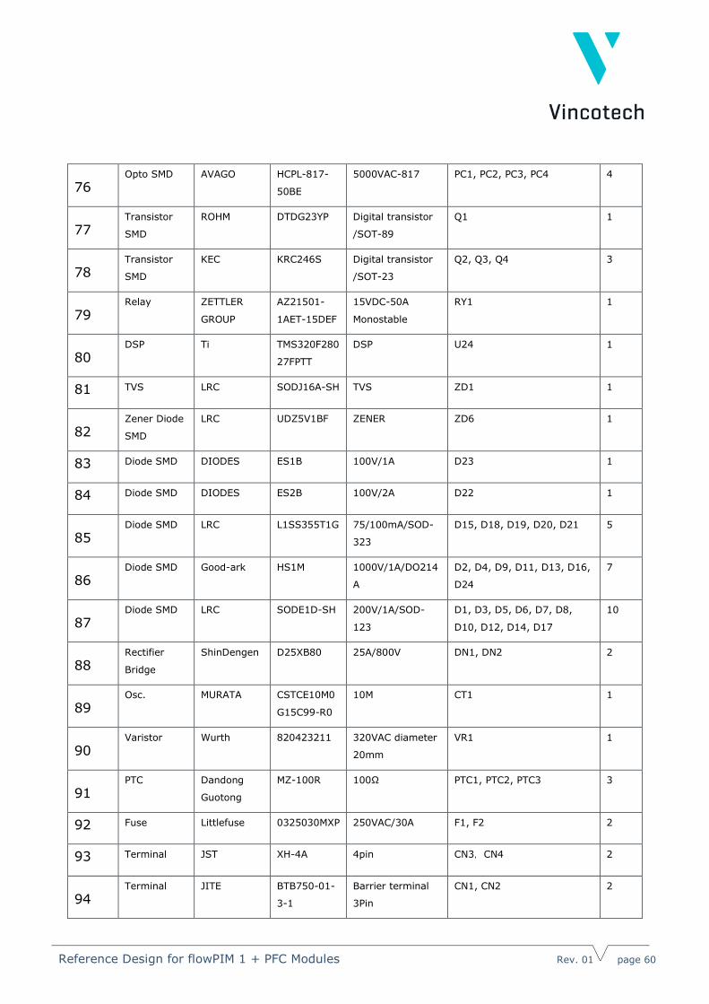
Reference Design for flowPIM 1 + PFC Modules Rev. 01 page 60
76 Opto SMD AVAGO HCPL-817-
50BE
5000VAC-817 PC1, PC2, PC3, PC4 4
77 Transistor
SMD
ROHM DTDG23YP Digital transistor
/SOT-89
Q1 1
78 Transistor
SMD
KEC KRC246S Digital transistor
/SOT-23
Q2, Q3, Q4 3
79 Relay ZETTLER
GROUP
AZ21501-
1AET-15DEF
15VDC-50A
Monostable
RY1 1
80 DSP Ti TMS320F280
27FPTT
DSP U24 1
81 TVS LRC SODJ16A-SH TVS ZD1 1
82 Zener Diode
SMD
LRC UDZ5V1BF ZENER ZD6 1
83 Diode SMD DIODES ES1B 100V/1A D23 1
84 Diode SMD DIODES ES2B 100V/2A D22 1
85 Diode SMD LRC L1SS355T1G 75/100mA/SOD-
323
D15, D18, D19, D20, D21 5
86 Diode SMD Good-ark HS1M 1000V/1A/DO214
A
D2, D4, D9, D11, D13, D16,
D24
7
87 Diode SMD LRC SODE1D-SH 200V/1A/SOD-
123
D1, D3, D5, D6, D7, D8,
D10, D12, D14, D17
10
88 Rectifier
Bridge
ShinDengen D25XB80 25A/800V DN1, DN2 2
89 Osc. MURATA CSTCE10M0
G15C99-R0
10M CT1 1
90 Varistor Wurth 820423211 320VAC diameter
20mm
VR1 1
91 PTC Dandong
Guotong
MZ-100R 100Ω PTC1, PTC2, PTC3 3
92 Fuse Littlefuse 0325030MXP 250VAC/30A F1, F2 2
93 Terminal JST XH-4A 4pin CN3,CN4 2
94 Terminal JITE BTB750-01-
3-1
Barrier terminal
3Pin
CN1, CN2 2
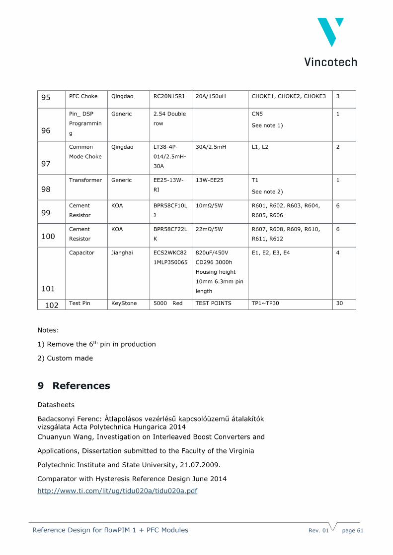
Reference Design for flowPIM 1 + PFC Modules Rev. 01 page 61
95 PFC Choke Qingdao RC20N15RJ 20A/150uH CHOKE1, CHOKE2, CHOKE3 3
96
Pin_ DSP
Programmin
g
Generic 2.54 Double
row
CN5
See note 1)
1
97
Common
Mode Choke
Qingdao LT38-4P-
014/2.5mH-
30A
30A/2.5mH L1, L2 2
98
Transformer Generic EE25-13W-
RI
13W-EE25 T1
See note 2)
1
99 Cement
Resistor
KOA BPR58CF10L
J
10mΩ/5W R601, R602, R603, R604,
R605, R606
6
100 Cement
Resistor
KOA BPR58CF22L
K
22mΩ/5W R607, R608, R609, R610,
R611, R612
6
101
Capacitor Jianghai ECS2WKC82
1MLP350065
820uF/450V
CD296 3000h
Housing height
10mm 6.3mm pin
length
E1, E2, E3, E4 4
102 Test Pin KeyStone 5000 Red TEST POINTS TP1~TP30 30
Notes:
1) Remove the 6th pin in production
2) Custom made
9 References
Datasheets
Badacsonyi Ferenc: Átlapolásos vezérlésű kapcsolóüzemű átalakítók
vizsgálata Acta Polytechnica Hungarica 2014
Chuanyun Wang, Investigation on Interleaved Boost Converters and
Applications, Dissertation submitted to the Faculty of the Virginia
Polytechnic Institute and State University, 21.07.2009.
Comparator with Hysteresis Reference Design June 2014
http://www.ti.com/lit/ug/tidu020a/tidu020a.pdf