Embed Size (px)
Citation preview
ARTICLE IN PRESS
Physica B 404 (2009) 4476–4481
Contents lists available at ScienceDirect
Physica B
0921-45
doi:10.1
� Corr
Portuga
E-m
journal homepage: www.elsevier.com/locate/physb
Role of impurities and dislocations for the unintentional n-typeconductivity in InN
V. Darakchieva a,b,c,�, N.P. Barradas a,b, M.-Y. Xie c, K. Lorenz a,b, E. Alves a,b, M. Schubert d,P.O.A. Persson c, F. Giuliani c, F. Munnik e, C.L. Hsiao c,f, L.W. Tu f, W.J. Schaff g
a Instituto Tecnologico e Nuclear, 2686-953 Sacav�em, Portugalb CFNUL, 1649-003 Lisboa, Portugalc IFM, Linkoping University, SE-581 83 Linkoping, Swedend Department of Electrical Engineering, University of Nebraska, Lincoln, NE 68588, USAe Forschungszentrum Dresden Rossendorf, 01314 Dresden, Germanyf Department of Physics and Center for Nanoscience and Nanotechnology, National Sun Yat-Sen University, Kaohsiung 80424, Taiwan, ROCg Department of Electrical and Computer Engineering, Cornell University, Ithaca, NY 14853, USA
26/$ - see front matter & 2009 Elsevier B.V. A
016/j.physb.2009.09.042
esponding author at: Instituto Tecnologico e
l.
ail address: [email protected]; [email protected] (V
a b s t r a c t
We present a study on the role of dislocations and impurities for the unintentional n-type conductivity
in high-quality InN grown by molecular beam epitaxy. The dislocation densities and H profiles in films
with free electron concentrations in the low 1017 cm�3 and mid 1018 cm�3 range are measured, and
analyzed in a comparative manner. It is shown that dislocations alone could not account for the free
electron behavior in the InN films. On the other hand, large concentrations of H sufficient to explain, but
exceeding substantially, the observed free electron densities are found. Furthermore, enhanced
concentrations of H are revealed at the film surfaces, resembling the free electron behavior with
surface electron accumulation. The low-conductive film was found to contain C and it is suggested that
C passivates the H donors or acts as an acceptor, producing compensated material in this case.
Therefore, it is concluded that the unintentional impurities play an important role for the unintentional
n-type conductivity in InN. We suggest a scenario of H incorporation in InN that may reconcile the
previously reported observations for the different role of impurities and dislocations for the
unintentional n-type conductivity in InN.
& 2009 Elsevier B.V. All rights reserved.
1. Introduction
Recent developments in group-III nitride technology have ledto the commercialization of a variety of optoelectronic deviceswith large impact on everyday life. In particular, high-brightnessblue and white light emitting diodes based on InGaN promisemore efficient lighting solutions [1]. An emerging potentialapplication of InGaN and InAlN alloys is in highly efficientmultijunction solar cells [2]. Furthermore, InN and related alloysare promising for developing high-frequency transistors, THzemitters and chemical sensors. Driven by the attractive materialapplications, the epitaxial techniques to grow InN and relatedalloys have made significant advances and matured during thelast decade. However, the poor understanding of the dopingmechanism in InN and the related In-rich alloys is one of the
ll rights reserved.
Nuclear, 2686-953 Sacav�em,
. Darakchieva).
critical issues that hinder further progress in the InN basedtechnology towards full exploitation of the material potential.
Understanding and controlling doping mechanisms in semi-conductors are indispensable for their incorporation into newelectronic devices, and challenge scientists to unravel the physicsbehind the sometimes peculiar free charge carrier generatingmechanisms. As a result of its exceptional propensity for n-typedoping [3] all unintentionally doped InN is n-type conductive butthe exact doping mechanism is under debate [4–10]. Difficulties toassess doping in InN and In rich alloys are encountered because ofthe presence of electron accumulation at the film surfaces withsurface charge densities ranging from 1013 to 3� 1014 cm�2.Electrical measurements are dominated by the accumulation layerconductivity, complicating their interpretation, since the exactcurrent paths are difficult to determine. The latter are required inorder to assign separately the free-charge carrier densities andmobilities to the individual layers of a sample.
The free electron concentration in InN films measured by singlefield electrical Hall effect was found to decrease with increasingfilm thickness. Some models derived on the basis of such electricalmeasurements favor positively charged N vacancies, V þN associated

ARTICLE IN PRESS
V. Darakchieva et al. / Physica B 404 (2009) 4476–4481 4477
with dislocations as the major origin of the thickness dependentunintentional bulk doping [5,8]. On the other hand, the electricalHall effect electron concentrations were also reported to correlatewith unintentional impurities, such as H and O [4,7]. Indeed, arecent theoretical study reported lower formation energies andthus higher equilibrium concentrations of H donors (H2þ
N and Hi)in comparison with VN , suggesting H as the plausible cause of theunintentional doping in InN [9]. We have recently reported also adecrease of the bulk free electron concentration with filmthickness measured by the contactless optical Hall effect [10,11].The variation of the bulk free electron concentration with filmthickness, however, does not follow the electrical Hall effectmodels accounting for a constant background electron concentra-tion and free electrons generated by nitrogen vacancies alongdislocations [10,11]. These findings indicated the existence of anadditional thickness-dependent doping mechanism and motivatethe need of further investigations in view of the existingcontroversy.
An argument in favor of the native defects as dominant donorspecies over the unintentional impurities is sometimes the lowbackground impurity concentrations in InN films [8,12]. The latterare often measured by secondary ion mass spectrometry (SIMS),which largely relies on the use of standards and may introducesignificant uncertainties in the impurity concentrations. On theother hand, ion beam analysis techniques, such as elastic recoildetection analysis (ERDA), measure directly the impurity concen-trations and depth profiles, and can provide valuable insights inthis respect. In this work we study the role of dislocations andimpurities for the unintentional doping in InN films with bulk freeelectron concentrations in the low 1017 cm�3 and mid 1018 cm�3
range using a combination of infrared spectroscopic ellipsometry(IRSE), transmission electron microscopy (TEM), X-ray diffraction(XRD) and ERDA.
2. Experimental
State-of-the-art unintentionally n-type doped InN films with(0 0 0 1) orientations and thicknesses of 1.3 and 1:6mm weregrown on sapphire substrates by molecular beam epitaxy (MBE).An in-situ GaN/AlN buffer sequence and a 1-mm-thick GaNtemplate layer grown by MBE were employed for the growth ofthe thicker (sample A) [13] and thinner (sample B) InN layers [14],respectively.
The free electron properties in the InN films were measured byinfrared spectroscopic ellipsometry (IRSE) using a rotatingcompensator infrared ellipsometer (J.A. Woollam Co., Inc.) in thespectral range of 35022000 cm�1 with a spectral resolution of2 cm�1, and at 603 and 703 angles of incidence. The IRSE data wereanalyzed by employing anisotropic dielectric functions of sap-phire and InN in the model calculations. The sapphire dielectricfunctions reported in Ref. [15] were used in the data analysis.Contributions of the IR active polar phonons to the InN modeldielectric function (MDF) were accounted for by a productpresentation of harmonic oscillator lineshapes with Lorentzianbroadening [16–18]. The free-carrier contributions were ac-counted for by the classical Drude model [16–18]. The parametersof the InN MDF and layer thickness were varied until measuredand calculated IRSE data simultaneously matched for all spectraldata points. As a result, the phonon mode parameters, the high-frequency limit of the dielectric function, the thickness, the freeelectron concentration and mobility in the InN films have beendetermined.
Transmission electron microscopy (TEM) specimens wereprepared by focused ion beam milling using a Zeiss 1540 EsBcross beam instrument following the lift out technique. The
cross-sectional TEM images were obtained in a FEI Tecnai G2 ultratwin microscope operating at 200 KV.
Elastic recoil detection analysis (ERDA) measurements wereperformed with 2 MeV 4Heþ ions at a tilt angle of 783 to measurethe H profiles in the films. The spectra were collected with aSchottky barrier detector placed at 243 scattering angle in IBMgeometry. To prevent scattered 4Heþ particles from hitting theERDA detector, a Kapton foil with a thickness of 8mm was placedin front of it. In addition, heavy ion (HI) ERDA with a 35Cl7þ
35 MeV beam was performed, with backscattered Cl and recoilsdetected with a Bragg chamber, and H detected simultaneouslywith a surface barrier Si detector using an Al foil to stop thescattered Cl beam. All data were analyzed with the IBADataFurnace NDF [19].
X-ray diffraction (XRD) was performed using a Philips tripleaxis diffractometer with a parabolic graded multilayer mirrorcollimator, followed by a channel-cut 2-bounce Ge(2 2 0) mono-chromator on the primary side and an asymmetric 2-bounceGe(2 2 0) analyzer [20].
3. Results and discussion
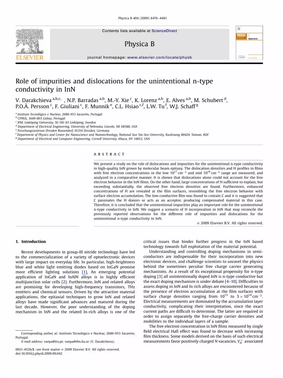
Fig. 1 shows scanning electron micrographs of the two InNsamples. The surface of the low conductive film A is ratherpeculiar displaying the presence of craters [indicated by C inFig. 1(a)], hillocks [indicated by H in Fig. 1(a)] and flat areas[indicated by F in Fig. 1(a)]. The diameters of the craters varybetween 1 and 10mm and the higher magnification image of thehillocks [Fig. 1(a), right panel] reveals that they consist of smallcrystallites blistering from the surface. Energy dispersive X-ray(EDX) spectra taken from the different areas of film A indicate thatthe flat areas and the hillocks have similar In content, and no Indroplets could be detected in any area type of the film. Very strongEDX Ga signal (� 50 at%) and negligible In signal in the cratersindicate that they most likely extent to the GaN buffer layer. Incontrast to film A, the surface morphology of film B is very smoothwith fine grain structure [Fig. 1(b)].
Fig. 2 shows experimental and best-model calculated IRSEspectra for the two InN films. The best-model calculated andexperimental data are in very good agreement. The InN films werefound to be constituted of a bulk, with a lower free electronconcentration, Nb and a thin surface layer (thickness ds) with ahigher electron charge accumulation concentration, Ns. Theelectron concentration in the GaN buffer layers turned out to bebelow the detection limit of the IRSE technique, which can beestimated to be approximately 1� 1017 cm�3 for n-type GaN [21].The free electron concentrations extracted from the best-matchmodeling to the experimental IRSE spectra of the two InN films aresummarized in Table 1. The bulk free-electron concentrations, Nb,(also given above the respective spectra in Fig. 2) are 1:970:1�1017 and 4:7170:04� 1018 cm�3, respectively. The surfaceelectron sheet densities, provided by the product Nsds, are1:070:7� 1013 and 0:370:1� 1013 cm�2 for sample A (lowconductive) and sample B (highly conductive), respectively. Thedrastic changes in the IRSE spectra in Fig. 2 are primarily caused bythe different bulk free electron concentrations of 1:9� 1017 and4:71� 1018 cm�3 in the two InN films. For high Nb values the freeelectrons effectively screen the polar phonons of sapphire, GaNbuffer and InN. Hence, the spectral features due to the A1(LO)phonons appear strongly damped. In particular, the large dip in Cfor the low conductive film near the InN uncoupled A1(LO) phononat about 594 cm�1[Fig. 2(a)] vanishes for the film with high Nb
[Fig. 2(b)] due to strong LO–phonon–plasmon coupling [22].Fig. 3 shows bright field TEM micrographs of the two InN films,
recorded with the electron beam parallel to /1 1 2 0S, which
ARTICLE IN PRESS
2 µm
2 µm
25 µm
C
H
F
F
H
Fig. 1. Scanning electron micrographs of the two InN films (a) sample A—InN thickness of 1:6mm grown on GaN/AlN buffer layer—under two different magnifications and
(b) sample B—InN thickness of 1:3mm grown on MBE GaN template. The morphological features in (a) are indicated as follows: flat areas, F—red circles; hillocks,
H—dashed blue circles and craters, C—black arrows. The right panel of (a) shows the hillocks at higher magnification. (For interpretation of the references to the color in
this figure legend, the reader is referred to the web version of this article.)
V. Darakchieva et al. / Physica B 404 (2009) 4476–44814478
provides contrast with all present threading dislocations. Thinhighly defective InN regions (� 250 nm thick) can be seen at theinterface with the GaN buffer layer for both samples [Figs. 3(a)and (b)]. Above the interfacial region the dislocation density isestimated to vary only marginally with film thickness, from1:770:2� 1010 to 0:970:3� 1010 cm�2 for the InN film inFig. 3(a) and from 3:170:1� 1010 to 2:470:3� 1010 cm�2 forthe InN film in Fig. 3(b) (see also Table 1). These results are inagreement with previous findings that the major change indislocation density in InN takes place within the substrate/buffer interfacial region of the InN film [23].
The fact that the dislocation density varies only marginallywith thickness has also been confirmed separately for screw andedge type dislocations with dark field TEM imaging with differentg-vectors (not shown here). The dark field TEM images reveal thatthe film with Nb of 4:71� 1018 cm�3 may contain slightly largernumbers of screw and mixed dislocations compared to edge type
dislocations. On the other hand, the edge type dislocations in thelow conductive film are found to be slightly larger in density thandislocations with screw component. To exclude the possibility ofany local peculiarities in the dislocation contents we have alsoestimated the densities of dislocations from XRD. The density ofedge dislocations, De, can be estimated from the full width at halfmaximum of the InN ð3 0 3 2Þ rocking curve, FWHM3032, asDe ¼ ð1:2FWHM
3032Þ2=ð4:35b2Þ, where b¼ 0:57033 nm [24]. We
estimated for our films De ¼ 1:8� 1010 cm�2 for the low con-ductive InN film A and Ne ¼ 1:1� 1010 cm�2 for the highlyconductive InN film B, confirming the TEM observations.
The only marginal variation of dislocation densities across ourfilms is in contrast to the large decrease of dislocation densitiesfrom low 1011 cm�2 to mid 109 cm�2 range over a thickness of122mm, previously observed for MBE InN films grown onsapphire using AlN buffer layers [6]. Similar scaling factors forthe density of dislocations and bulk electron concentration

ARTICLE IN PRESS
Fig. 2. Experimental (circles) and best-model (solid lines) IRSE C spectra for the
InN films with (a) sample A with thickness of 1:6mm and Nb ¼ 1:9� 1017 cm�3 and
(b) sample B with thickness of 1:3mm and Nb ¼ 4:71� 1018 cm�3. The bulk, Nb
electron densities are indicated above the respective spectra and the phonon
modes of InN and the sapphire substrate are indicated with brackets (solid and
dashed lines indicate TO and LO phonons, respectively).
Table 1Best-model IRSE free electron densities, dislocation densities estimated from TEM
and XRD, and H and C concentrations for the InN films: bulk free electron
concentration, Nb , surface electron sheet density, Nsds , TEM density of dislocations
in the surface, Ds , and interface region, Di , density of edge type dislocations
estimated from XRD, De , total amount of surface hydrogen, [H]s , bulk hydrogen
concentration, ½H�b , and bulk carbon concentration, [C].
Sample A B
Nb (1017 cm�3) 1:970:1 47:170:5
Nsds (1013 cm�2) 1:070:1 0:370:1
Di (1010 cm�2) 1:770:2 3:170:1
Ds (1010 cm�2) 0:970:3 2:470:3
De (1010 cm�2) 1.8 1.1
Hs (1016 cm�2) 4:870:1 1:7970:03
Hb (at%) 0:670:1 0:0570:03
C (at%) 1:070:5 –
GaN
500 nm
InN
500 nm
GaN
InN
Fig. 3. Cross-section bright-field TEM images with the diffraction vector parallel to
/1 1 2 0S of (a) sample A and (b) sample B.
Fig. 4. ERDA Hydrogen profiles of (a) sample A and (b) sample B.
V. Darakchieva et al. / Physica B 404 (2009) 4476–4481 4479
measured by electrical Hall effect were also reported in thisprevious work concluding on the major role of the dislocations forthe unintentional n-type conductivity in InN [6,5]. Our presentTEM findings of nearly unchanged dislocation density with filmthickness indicate that dislocations could not play the dominantrole for the thickness dependent unintentional conductivity forour InN grown on GaN buffers or templates, which is in agreementwith our previous optical Hall effect observations [10]. Moreimportantly, we find here similar densities of dislocations in InNfilms with bulk electron concentrations that differ by more thanan order of magnitude suggesting that different donor defect(s)unrelated to dislocations must be present. Unintentional impu-rities, such as H, O and Si are the obvious candidates.
Fig. 4 shows the H profiles measured by Heþ ERDA in the twoInN films. A significant enhancement of the H concentration isobserved at the surfaces of the two films. This H profile could matchthe profile of free electron carriers at the surfaces of the InN sampleswith large accumulation of electrons. The results were alsoconfirmed by the HI-ERDA and the estimated impurityconcentrations are given in Table 1. Note that a higher totalamount of H in the surface region is measured for the film withthe higher surface sheet density. These observations indicate that Hmight play an important role for the surface charge properties inInN. High H concentrations of 0:670:1 at% and 0:0570:03 at% arealso measured in the bulk of the InN films with Nb ¼ 1:9�1017 cm�3 (sample A) and Nb ¼ 4:71� 1018 cm�3 (sample B),respectively. It is worth mentioning that we have detectedhydrogen in a large number of InN films grown with differentsurface orientations, thicknesses, doping and at four different growthlaboratories and detailed studies on the subject will be reportedelsewhere. In all cases the bulk H concentrations are sufficient toexplain, but exceed substantially, the bulk electron concentrations. Itis possible that part of the H is present in electrically inactive sites orcomplexes. The enhanced surface concentrations of H measured inthe films (Table 1 and Fig. 4) strongly suggest that post growthsurface contamination by H is taking place in InN, most probably as aresult of the samples exposure to ambient atmosphere. Therefore,certain amount of H could be incorporated in the bulk of the filmsafter growth via diffusion from the near-surface regions. Note thatthe different surface morphologies (see Fig. 1) may tolerate differentH incorporation in the surface regions while the specific filmmicrostructure is expected to affect the diffusion giving rise to rathercomplex H behavior. Indeed, the total amount of surface hydrogen ismuch higher in film A with much rougher surface morphology (seeFig. 1 and Table 1). It is also possible that the surface morphology of

ARTICLE IN PRESS
total C
surface O
total N
total N
k
Fig. 5. HI-ERDA profiles of (a) sample A and (c) sample B. Integrated yields over the windows indicated in (a) and (c) and projected on the Bragg peak height axes are
displayed in (b) and (d) for the A and B films, respectively.
V. Darakchieva et al. / Physica B 404 (2009) 4476–44814480
film A is partly a consequence of the large amount of hydrogen in thefilm, which may provoke blistering.
We note that the scenario of surface H incorporation andsubsequent diffusion suggested here may also effectively explainthe previously reported different observations for the role ofdislocations and impurities for the unintentional n-type conductivityin InN [4–8,10]. Naturally, films grown at similar conditions andnucleation schemes, and having similar sample histories areexpected to incorporate similar amounts of hydrogen in the nearsurface regions. Then the H diffusion in the bulk will be mainlygoverned by the film microstructure and films with higher densitiesof dislocations will show higher bulk free electron concentrations.Findings correlating the free electron concentration to dislocationdensity are reported in Refs. [5,6] and consistent with our scenario.Whenever the InN films are grown at different conditions or/andhave different sample histories, such as in the present study, the bulkfree electron concentration could no longer be uniquely correlated tothe dislocation density. This is also in agreement with our previousOptical Hall effect study of a series of InN films [10,11]. Thesuggested scenario could also explain previous findings correlatingthe amounts of H to the free electron concentrations in InN [4,7].
Interestingly, the low conductive film A shows higher amount ofH compared to the film B with the higher free electron concentra-tion. We also found that the bulk H concentration varies in different
areas of these films. The HI-ERDA results [Figs. 5(a) and (b)] furthershow the presence of C impurities in the low-conductive film,estimated to be 1:070:5 at%. C may act as an acceptor in InNcompensating the H donors and thus explaining the low freeelectron concentration in this film. Indeed, a recent theoretical studyhas concluded that substitutional C on the N site, CN , has the lowestformation energy and acts as a single acceptor [25]. It is also possiblethat C forms complexes with H passivating the H donors rather thancompensating them. The large electron mobility in film A of1600 cm2=ðV sÞ speaks in favor of the latter speculation, however,more work is required to clarify this issue. Some surface O close tothe detection limit of 0.5 at% could also be resolved for the lowconductive film [Figs. 5(a) and (b)], which in addition will affect thesurface charge properties in this case. No additional impurities couldbe detected in the bulk of the InN films from the HI-ERDA profiles(Fig. 5).
4. Conclusions
The role of dislocations and impurities for the unintentionaln-type conductivity in state-of-the-art MBE InN has beenstudied. TEM investigations, corroborated with XRD, revealedsimilar densities of dislocations in films with bulk electron

ARTICLE IN PRESS
V. Darakchieva et al. / Physica B 404 (2009) 4476–4481 4481
concentrations that differ by more than an order of magnitude.This finding strongly suggests that native defects along disloca-tions could not play a dominant role for the unintentional n-typedoping in MBE InN films grown on GaN buffers or templates. Thisassertion is further supported by the fact that the dislocationdensities change only marginally across the films and thus couldnot alone explain the previously reported decrease of bulkelectron density with increasing film thickness for films grownusing similar nucleation schemes. On the other hand, we foundsignificant concentrations of H in the InN films sufficient toexplain, but substantially exceeding, the measured bulk electronconcentrations. The H profiles revealed enhanced concentrationsat the film surfaces, resembling the free electron behavior withsurface electron accumulation. Furthermore, a large concentra-tion of C is found in the low conductive film and it is suggestedthat C acts as an acceptor, in corroboration with a recenttheoretical study [25], compensating the H donors or formscomplexes with H passivating the H donors in this case.Therefore, it is concluded that unintentional impurities, such asH and C, play an important role for the unintentional n-typeconductivity in InN.
Acknowledgments
VD gratefully acknowledges Prof. B. Monemar for valuablediscussions, continuous support, and encouragement. This work isfinancially supported by FCT Portugal under program Ciencia2007 and contract PTDC/FIS/100448/2008, and by the SwedishResearch Council (VR) under contract 2005-5054. The HI-ERDAwork is supported by EU-‘‘Research Infrastructures TransnationalAccess’’ program AIM ‘‘Center for Application of Ion Beams inMaterials Research’’ under EC contract no. 025646. Financialsupport from NSF MRSEC (DMR-0820521), U.S. Army ResearchOffice (W911NF-08-C-0111), and J.A. Woollam Foundation isacknowledged.
References
[1] E.F. Schubert, Light-emitting Diodes, Cambridge University Press, Cambridge,UK, 2003.
[2] L. Hsu, W. Walukiewicz, J. Appl. Phys. 104 (2008) 024507.[3] W. Walukiewicz, Physica B 302 (2001) 123.[4] D.C. Look, H. Lu, W.J. Schaff, J. Jasinski, Z. Liliental-Weber, Appl. Phys. Lett. 80
(2002) 258.[5] V. Cimalla, V. Lebedev, F.M. Morales, R. Goldhahn, O. Ambacher, Appl. Phys.
Lett. 89 (2006) 172109.[6] V. Lebedev, V. Cimalla, T. Baumann, O. Ambacher, F.M. Morales, J.G. Lozano,
D. Gonz�alez, J. Appl. Phys. 100 (2006) 094903.[7] C.S. Gallinat, G. Koblmuller, J.S. Brown, S. Bernardis, J.S. Speck, G.D. Chern,
E.D. Readinger, H. Shen, M. Wraback, Appl. Phys. Lett. 89 (2006) 032109.[8] L.F.J. Piper, T.D. Veal, C.F. McConville, H. Lu, W.J. Schaff, Appl. Phys. Lett. 88
(2006) 252109.[9] A. Janotti, C.G. Van de Walle, Appl. Phys. Lett. 92 (2008) 032104.
[10] V. Darakchieva, T. Hofmann, M. Schubert, B.E. Sernelius, B. Monemar,P.O.A. Persson, F. Giuliani, E. Alves, H. Lu, W.J. Schaff, Appl. Phys. Lett. 94(2009) 022109.
[11] T. Hofmann, V. Darakchieva, B. Monemar, H. Lu, W.J. Schaff, M. Schubert,J. Electron. Mater. 37 (2008) 611.
[12] W. Walukiewicz, J.W. Ager III, K.M. Yu, Z. Liliental-Weber, J. Wu, S.X. Li,R.E. Jones, J.D. Denlinger, J. Phys. D: Appl. Phys. 39 (2006) R83.
[13] H. Lu, W.J. Schaff, J. Hwang, H. Wu, G. Koley, L.F. Eastman, Appl. Phys. Lett. 79(2001) 1489.
[14] C.-T. Liang, Z.H. Sun, C.L. Hsiao, Z.M. Hsu, L.W. Tu, J.-Y. Lin, L.C. Chen, J.H. Chen,Y.F. Chen, C.T. Wu, Appl. Phys. Lett. 90 (2007) 172101.
[15] M. Schubert, T.E. Tiwald, C.M. Herzinger, Phys. Rev. B 61 (2000) 8187.[16] V. Darakchieva, T. Paskova, M. Schubert, P.P. Paskov, H. Arwin, B. Monemar,
D. Hommel, M. Heuken, J. Off, F. Scholz, B.A. Haskell, P.T. Fini, J.S. Speck,S. Nakamura, Phys. Rev. B 75 (2007) 195217.
[17] V. Darakchieva, Phys. Status Solidi A 205 (2008) 905.[18] M. Schubert, Infrared Ellipsometry on Semiconductor Layer Structures:
Phonons, Plasmons and Polaritons, vol. 209, Springer, New York, 2004.[19] N.P. Barradas, C. Jeynes, R.P. Webb, Appl. Phys. Lett. 71 (1997) 291.[20] V. Darakchieva, T. Paskova, P.P. Paskov, B. Monemar, N. Ashkenov, M. Schubert,
J. Appl. Phys. 97 (2005) 013537.[21] A. Kasic, M. Schubert, S. Einfeldt, D. Hommel, T. Tiwald, Phys. Rev. B 62 (2000)
7365.[22] V. Darakchieva, P.P. Paskov, E. Valcheva, T. Paskova, M. Schubert,
C. Bundesmann, H. Lu, W.J. Schaff, B. Monemar, Superlattices and Micro-structures 36 (2004) 573.
[23] H. Lu, W.J. Schaff, L.F. Eastman, C.E. Stutz, Appl. Phys. Lett. 82 (2003) 1736.[24] X. Wang, S.-B. Che, Y. Ishitani, A. Yoshikawa, Appl. Phys. Lett. 90 (2007)
151901.[25] X.M. Duan, C. Stampfl, Phys. Rev. B 79 (2009) 035207.


