Embed Size (px)
Citation preview
IOP PUBLISHING SEMICONDUCTOR SCIENCE AND TECHNOLOGY
Semicond. Sci. Technol. 27 (2012) 015007 (11pp) doi:10.1088/0268-1242/27/1/015007
Concentration of uncompensatedimpurities as a key parameter of CdTeand CdZnTe crystals for Schottky diodex/γ-ray detectorsL A Kosyachenko1, C P Lambropoulos2, T Aoki3, E Dieguez4,M Fiederle5, D Loukas6, O V Sklyarchuk1, O L Maslyanchuk1,E V Grushko1, V M Sklyarchuk1, J Crocco4 and H Bensalah4
1 Chernivtsi National University, 58012 Chernivtsi, Ukraine2 Technological Educational Institute of Chalkida, Psahna, Evia, GR 34400, Greece3 Research Institute of Electronics, Shizuoka University, Johoku, Hamamatsu 432-8011, Japan4 Crystal Growth Laboratory, Universidad Autonoma de Madrid, 28049 Madrid, Spain5 Freiburger Materialforschungszentrum, Albert Ludwigs Universitat, D-79104 Freiburg, Germany6 Institute of Nuclear Physics, NCSR Demokritos, 15310 Athens, Greece
E-mail: [email protected]
Received 23 August 2011, in final form 2 November 2011Published 7 December 2011Online at stacks.iop.org/SST/27/015007
AbstractIn this paper we report on the strong impact of the concentration of uncompensated impuritieson the detection efficiency of CdTe and Cd0.9Zn0.1Te Schottky diodes. The results of our studyexplain the observed poor detection properties of some Cd0.9Zn0.1Te detectors with resistivityand lifetime of carriers comparable to those of good CdTe detectors. We show that theconcentration of uncompensated impurities in a highly efficient CdTe Schottky diode detectoris several orders of magnitude higher than that of a CdZnTe, which does not register the gammaspectra of commonly used isotopes (59–662 keV) by using photoelectric measurements. Thesignificant difference of the concentration of uncompensated impurities between CdTe andCd0.9Zn0.1Te crystals is confirmed by our study of the temperature change of the resistivity andof the Fermi level energy. The degree of compensation of the donor complex, responsible forthe electrical conductivity of the material, is much lower in the CdTe crystal compared to thatin the Cd0.9Zn0.1Te crystal. The calculations of the detection efficiency of x/γ -radiation by aSchottky diode result in a dependence on the concentration of uncompensated impuritiesdescribed by a curve with a pronounced maximum. The position of this maximum occurs at aconcentration of uncompensated impurities which ranges from 3 × 10¹⁰ to 3 × 1012 cm−3
depending on the registered photon energy of x/γ -rays and on the lifetime of the chargecarriers. Our measurements and calculations lead to the conclusion that the concentration ofuncompensated impurities in this range is a necessary condition for the effective operation ofx- and γ -ray Schottky diode detectors based on CdTe and Cd1−xZnxTe crystals.
(Some figures in this article are in colour only in the electronic version)
1. Introduction
High resistivity and long lifetime of charge carriers arenecessary for the effective operation of x- and γ -ray detectors
based on CdTe and Cd1−xZnxTe, which are widely used invarious fields of science and technology. Long lifetime andstrong electric field increase the charge collection efficiency.High resistivity reduces the leakage current and consequently
0268-1242/12/015007+11$33.00 1 © 2012 IOP Publishing Ltd Printed in the UK & the USA
Semicond. Sci. Technol. 27 (2012) 015007 L A Kosyachenko et al
the shot noise component. For this reason either thermoelectriccooling [1] or Schottky [2] and p–n diodes [3] are used.
The transition from CdTe to Cd1−xZnxTe (x = 0.1–0.2)leads to a marked increase of the resistivity of the materialbecause the band gap widens. The use of a Schottky contactresults in an even greater reduction of the leakage current.However, from the study of the samples of CdZnTe Schottkydiode detectors it turns out that their detection efficiency ismuch lower than that of CdTe Schottky diodes in many cases.Consequently, one can make the reasonable assumption thatsome other material parameters affect the efficiency of theCdTe and CdZnTe detectors.
In a Schottky diode, the space charge region (SCR) is theactive region of the detector and there is no doubt that the widthof the SCR is an important parameter of the devices. Even ifthe Schottky contact is not created intentionally, band bendingat the surface of a semi-insulating CdTe or CdZnTe crystalcreates a SCR at the contacts. Space charge layers adjacentto these ‘ohmic’ contacts can have a significant impact on theproperties of the detector, because they lead to changes in thecharge transport mechanism and in the carrier lifetimes.
Typically, CdTe and Cd1−xZnxTe crystals are doped by Clor In donor impurities (up to 1016–1018 cm−3). It is known thatdoping with elements of the III and VII groups of the periodicsystem is accompanied by the self-compensation effect. Thiseffect consists of the fact that the donor impurity most oftenforms a complex with an acceptor type vacancy (associate,center) and it is used widely to create a semi-insulating state ofthe material [4–7]. In this paper we proceed from the dominantrole of such complexes, which are formed by the intentionaldoping of the CdTe crystals with Cl and of the CdZnTe crystalswith In. We assume that the Fermi level position in the bandgap, which provides the nearly intrinsic conductivity of theCdTe and Cd1−xZnxTe crystals, is determined in both casesby the ionization energy and the degree of compensation ofthe donor impurity (Cl or In) included in the complex [6–9].7
The width of the SCR of a Schottky diode based on such asemiconductor is given by
W =√
2εεo(ϕo − qV )
q2(Nd − Na), (1)
where ε is the relative semiconductor permittivity, εo isthe electric constant, ϕo is the barrier height from thesemiconductor side, q is the electron charge, V is the appliedvoltage and Nd–Na is the concentration of uncompensateddonors. Thus, the concentration of uncompensated impuritiesNd–Na determines the width of the space-charge region atthe contacts along with the resistivity and the lifetime ofcharge carriers. Consequently this concentration, Nd–Na ,is the important parameter of the semiconductor used in thefabrication of Schottky diode detectors.
The width of the SCR (and hence the concentrationof uncompensated impurities) in semi-insulating CdTe andCdZnTe Schottky diodes cannot be determined with traditional
7 At a low degree of compensation of the donor impurity, the Fermi level is inthe upper half of the band gap and the semiconductor has n-type conductivity.With a higher compensation degree, the Fermi level shifts below the middle ofthe band gap, i.e. semiconductor acquires p-type conductivity (see section 4).
electrical measurements due to the presence of the high-resistance neutral part in the diode structure. However,important information about the SCR width can be obtainedby studying the spectral distribution of photoresponse of theSchottky diode (section 3). The temperature dependence of theFermi level energy is discussed in section 4. This dependenceprovides important information about the compensation degreeof the impurity responsible for the electrical conductivity ofthese crystals. Finally, section 5 presents the calculationresults of the detection efficiency of the Schottky diodedetectors as a function of the concentration of uncompensatedimpurities. It is proven that this concentration has an optimalrange, which maximizes the detection efficiency.
It should be noted that, to our knowledge, the effect of theconcentration of uncompensated impurities on the detectionproperties of x/γ -ray detectors based on CdTe and CdZnTe isnot discussed thoroughly in the literature.
2. Samples
We used for the fabrication of detectors CdTe crystals madeby the Acrorad Co., Ltd and Cd1−xZnxTe crystals grown bythe Freiburger Materialforschungszentrum and by the CrystalGrowth Laboratory of the Materials Physics Department of theUniversidad Autonoma de Madrid.
As we noted in the introduction, the Schottky diodedetectors fabricated with Cd1−xZnxTe crystals with appropriateresistivity and lifetime of charge carriers have inferiordetection efficiency than the Schottky diode detectorsfabricated with CdTe crystals and often they do not detectthe x/γ -radiation. To clarify the reasons for this we haveinvestigated two Cd0.9Zn0.1Te crystals with Schottky diodes:(i) CdZnTe-1, which registers the radiation of commonly usedisotopes, and (ii) CdZnTe-2, which does not register the X/γ -radiation.
We minimized the influence of uncontrollable differencesbetween the material used for the detectors and the samplesused for the study of the optical, electrical and photoelectricproperties by cutting these samples from the same piecesof crystal. The detectors have 5 × 5 mm2 area and 1 mmthickness. The area of the ohmic and of the Schottky contactson the opposite sides of the crystal is 4 × 4 mm2. Theplates for optical measurements have a thickness of about100 μm, while the samples for the study of the temperaturedependence of the resistivity have an area of 0.5 × 2 mm2
and a length of 5 mm. Both the ohmic and the Schottkycontact of the CdTe device were made by vacuum depositionof Ni after a preliminary chemical treatment and ion etching ofthe crystal surfaces. The parameters of the ion bombardmentwere different for the ohmic and the Schottky faces [10]. Theohmic and the Schottky contacts of the CdZnTe devices weremade by vacuum deposition of In and Ni, respectively. Forthe photoelectric measurements, the film of Ni which formedthe Schottky contact was made thin enough (10–12 nm) toprovide optical transparency of 70–75% in the wavelengthrange of 800–870 nm.
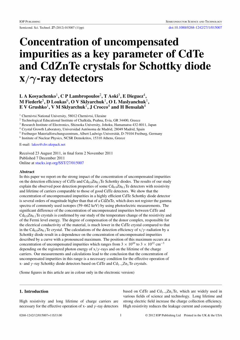
Figure 1 shows spectra of the 241Am (59.5 keV) and 137Cs(662 keV) isotopes recorded with Schottky diode detectors
2
Semicond. Sci. Technol. 27 (2012) 015007 L A Kosyachenko et al
241Am
30 40 50 60 70
0
50
100
hv (keV)
Cou
nts
(arb
. uni
ts)
CdZnTe-1
CdTe
137Cs
400 500 600 700 0
10
20
30
40
50
hv (keV)
Cou
nts
(arb
. uni
ts)
CdZnTe-1
CdTe
(a) (b)
Figure 1. Spectra of 241Am (a) and 137Cs (b) isotopes taken with Schottky diode detectors based on CdTe and CdZnTe-1.
1.45 1.47 1.49 1.51 1.53 1.550
10
20
30
40
hv (eV)
α2 (cm
–2)
CdZnTe-2
CdZnTe-1
CdTe
EgEg
2.8 3.0 3.2 3.4
1011
1010
107
108
109
1000/T
ρ ( Ω
⋅cm
)
CdZnTe-2
CdZnTe-1
CdTe
300 K
(b)(a)
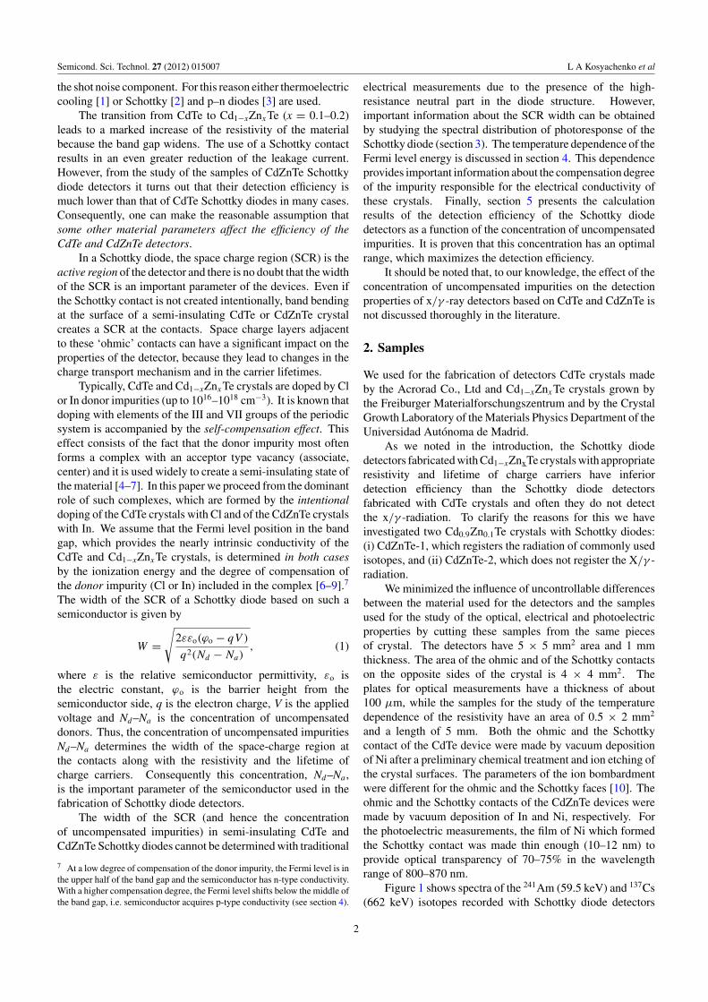
Figure 2. (a) Absorption curves α(hv) of CdTe and CdZnTe samples near the edge of optical transmission plotted as α2 versus hv fordetermining the band gaps of the materials. (b) Temperature dependence of the resistivity of the samples.
prepared with the CdTe crystal and with the CdZnTe-1 crystal.As already mentioned, the Schottky diode prepared with theCdZnTe-2 crystal does not register the x/γ -radiation.
As one can see from figure 1, the centroid of the 59.5 keVphotopeak in the 241Am spectrum of the CdZnTe-1 detectoris at lower energy. This proves that the charge collectionefficiency of this detector is inferior to the charge collectionefficiency of the CdTe detector. The 662 keV photopeak ishardly seen in the 137Cs spectrum of the CdZnTe-1 detector.The FWHM of the photopeak is broader in 241Am spectrumof the CdZnTe-1 detector and the shape of its 137Cs spectrummanifests the incomplete charge collection.
The band gap of the crystals has been extracted fromoptical measurements in the same way as described in [7].The derived values of Eg for CdTe are close to 1.47 eV at300 K and close to 1.48 eV at 290 K. The value of Eg forCdZnTe at T = 290–300 K is between 1.52 eV and 1.53 eV(figure 2(a)).
While the detection properties of the crystals are verydifferent, the resistivities ρ of CdTe, CdZnTe-1 and CdZnTe-2at room temperature are 6 × 10⁹, 8 × 10⁹ and 9 × 10¹⁰ �
cm, respectively, i.e. they are very close to each other. Atthe same time, the resistivities of the samples are close to thatof the material with intrinsic conductivity. In this case, thetemperature activation energy of resistivity �E should be equalto half the semiconductor band gap at T = 0, i.e. 0.80 eV forCdTe and 0.84 eV for Cd1−xZnxTe with x = 0.1. Meanwhile,the activation energies found from the slope of the straight linesin figure 2(b) are ‘abnormally’ low, namely, �E = 0.78, 0.76and 0.63 eV for CdTe, CdZnTe-1 and CdZnTe-2, respectively.It will be shown in section 4 that these features are explained interms of the statistics of electrons and holes in a compensatedsemiconductor with deep levels in the band gap.
It is necessary to know the lifetime of charge carriers forthe interpretation of the observed detector characteristics andfor the subsequent calculations: (i) the minority carrier lifetimedetermines the diffusion component of the photocurrent
3
Semicond. Sci. Technol. 27 (2012) 015007 L A Kosyachenko et al
0 5 10 15 20 251.0
10
100
t (μs)
I ph
(arb
. uni
ts)
CdTeτ = 2.1 µs
CdZnTe-2τ = 5.5 µs
CdZnTe-1τ = 3.5 µs
0 50 100 150 2001.0
10
100
t (ns)
τ = 85 ns
τ = 22 ns
CdTe τ = 17 ns
CdZnTe-1τ = 13 ns
CdZnTe-2
(a) (b)
Figure 3. Decay curves of the photocurrent excited by radiation from AlGaAs semiconductor laser in CdTe, CdZnTe-1 and CdZnTe-2crystals with ohmic contacts (a) and Schottky diode detectors (b).
excited in the neutral part of the crystal; (ii) the lifetime inthe SCR determines the collection efficiency of the chargecarriers in the SCR and of the excess carriers arising inthe neutral part of the crystal and reaching the SCR bydiffusion.
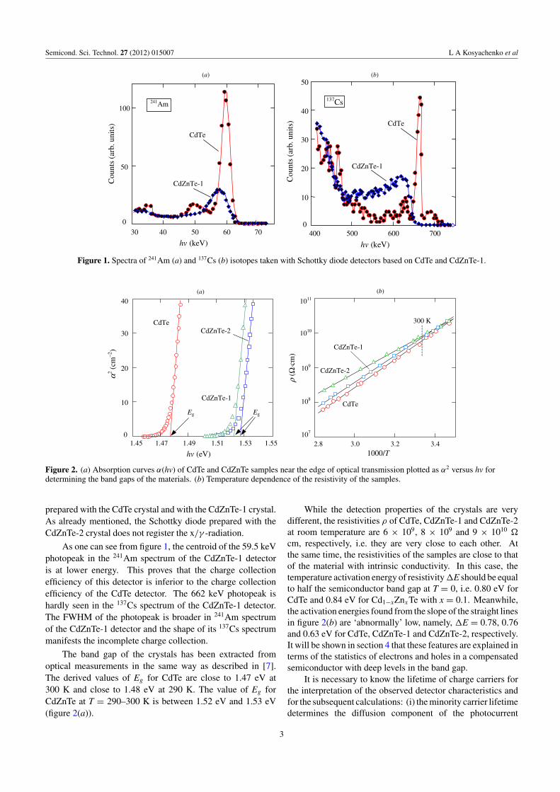
The charge states of impurities and defects in the SCRand in the neutral part of the crystal are different, so it canbe assumed that the lifetimes of charge carriers in differentparts of the crystal are also different. Their values canbe determined from the decay curves of the photocurrentexcited by rectangular pulses of a high-speed laser diode.Figure 3 presents the decay curves of the photocurrent in theCdTe, CdZnTe-1 and CdZnTe-2 crystals irradiated with laserpulses.
Figure 3(a) shows the decay curves of the photocurrent ofcrystals with ohmic contacts prepared by vacuum deposition ofa semitransparent metal layer. These decay curves apparentlyreflect the behavior of the excess photocarriers in the neutralpart of the diode structures. One expects that the photocurrentdecays exponentially Iph = Ipho·exp(−t/τ ) and consequentlyits relaxation curve will be a straight line if it is plotted insemilogarithmic coordinates. Indeed this is the case and theslope of the linear fit gives the value of the lifetime of thecharge carriers. This value is equal to 2.1, 3.5 and 5.5 μs forthe CdTe, CdZnTe-1 and CdZnTe-2 crystals, respectively.
Figure 3(b) shows the photocurrent decay curves of diodeswith semitransparent Ni Schottky contacts made on the CdTe,CdZnTe-1 and CdZnTe-2 crystals. The emission wavelengthof the laser was 782 nm, so excitation of photocarriers occurredin a thin surface layer of the semiconductor, that is, onlyin the SCR of the diode structure. Therefore, the observedrelaxation curves of the photocurrent reflect the processes inthe SCR. As can be seen, the lifetimes of charge carriers inthe SCR are in the range of 10–20 ns. These lifetimes aremuch shorter than those in the neutral region of the diodestructure. Additionally, the decay curve of the photocurrentof the CdZnTe-2 Schottky diode has two linear regions withdifferent slopes. This fact indicates a fast and a slower
relaxation process. The corresponding lifetimes found fromthe slopes of linear sections in figure 3(b) are 22 and 85 ns. Thisbehavior can be understood, since many levels in the band gapof the investigated crystals are available and potential variesas a function of depth in the SCR in complex ways.
3. Determination of Nd–Na from the photoresponsespectra of Schottky diode detectors
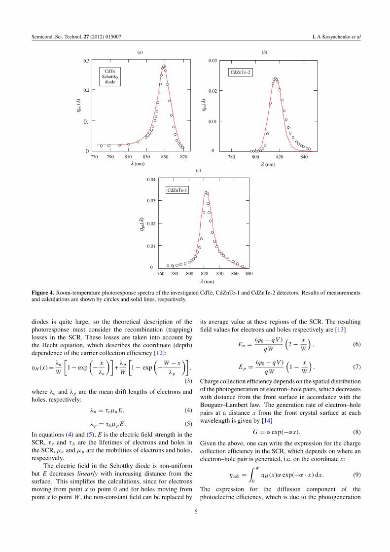
In this section, we present the measurements and thetheoretical calculations of the photoresponse spectra of theSchottky diode detectors. The measured photoresponsespectra of the CdTe, CdZnTe-1 and CdZnTe-2 detectors areshown in figure 4 by circles, when the detectors were irradiatedthrough the semitransparent Schottky contact. All the threespectra have a peak at a wavelength close to λg = hc/Eg . Asis shown below, it is possible to extract the concentration ofuncompensated donors Nd–Na in the materials used by fittingthe calculated results (solid lines) to the experimental curves.It turned out that the derived concentrations are very differentfor the CdTe, CdZnTe-1 and CdZnTe-2 detectors.
In the theoretical description of the photoresponse spectrawe assume that the photoelectric quantum yield of a Schottkydiode contains a drift and a diffusion component. Taking intoaccount recombination at the front surface, the drift componentof the quantum efficiency of a Schottky photodiode based ona p-type semiconductor can be represented as [11]
ηodrif =
1 + Sf
Dp
(α + 2
W
ϕo−qV
kT
)−1
1 + Sf
Dp
(2W
ϕo−qV
kT
)−1 − exp(−αW), (2)
where Sf is the recombination velocity at the front surface ofthe crystal, α is the light absorption coefficient, Dp is the holediffusion coefficient, which is correlated to the hole mobilityμp by the Einstein equation qDp/kT = μp.
Equation (2) does not account for recombination(trapping) losses inside the SCR. It follows from the resultsbelow that the width of the SCR in the studied Schottky
4
Semicond. Sci. Technol. 27 (2012) 015007 L A Kosyachenko et al
770 790 810 830 850 8700
0.
0.2
0.3
λ (nm)
η ph
(λ)
CdTe Schottky
diode
780 800 820 8400
0.01
0.02
0.03
CdZnTe-2
λ (nm)
η ph(
λ)
760 780 800 820 840 860 8800
0.01
0.02
0.03
0.04
CdZnTe-1
λ (nm)
η ph(
λ )
(a)
(c)
(b)
Figure 4. Room-temperature photoresponse spectra of the investigated CdTe, CdZnTe-1 and CdZnTe-2 detectors. Results of measurementsand calculations are shown by circles and solid lines, respectively.
diodes is quite large, so the theoretical description of thephotoresponse must consider the recombination (trapping)losses in the SCR. These losses are taken into account bythe Hecht equation, which describes the coordinate (depth)dependence of the carrier collection efficiency [12]:
ηH (x)= λn
W
[1− exp
(− x
λn
)]+
λp
W
[1 − exp
(−W − x
λp
)],
(3)
where λn and λp are the mean drift lengths of electrons andholes, respectively:
λn = τeμnE, (4)
λp = τhμpE. (5)
In equations (4) and (5), E is the electric field strength in theSCR, τ e and τh are the lifetimes of electrons and holes inthe SCR, μn and μp are the mobilities of electrons and holes,respectively.
The electric field in the Schottky diode is non-uniformbut E decreases linearly with increasing distance from thesurface. This simplifies the calculations, since for electronsmoving from point x to point 0 and for holes moving frompoint x to point W , the non-constant field can be replaced by
its average value at these regions of the SCR. The resultingfield values for electrons and holes respectively are [13]
En = (ϕ0 − qV )
qW
(2 − x
W
), (6)
Ep = (ϕ0 − qV )
qW
(1 − x
W
). (7)
Charge collection efficiency depends on the spatial distributionof the photogeneration of electron–hole pairs, which decreaseswith distance from the front surface in accordance with theBouguer–Lambert law. The generation rate of electron–holepairs at a distance x from the front crystal surface at eachwavelength is given by [14]
G = α exp(−αx). (8)
Given the above, one can write the expression for the chargecollection efficiency in the SCR, which depends on where anelectron–hole pair is generated, i.e. on the coordinate x:
ηcoll =∫ W
0ηH (x)α exp(−α · x) dx. (9)
The expression for the diffusion component of thephotoelectric efficiency, which is due to the photogeneration
5
Semicond. Sci. Technol. 27 (2012) 015007 L A Kosyachenko et al
800 810 820 8300
0.4
0.8
1.0
0.2
0.6
Nd–Na=1010 cm–3 109 cm–3 108 cm–3 107 cm–3
λ (nm)
S
pect
ral p
hoto
resp
onse
(ar
b. u
nits
)
800
805
810
815
820
825
1010109 108 107
λ max
(nm
)
Nd –Na (cm–3)
(a) (b)
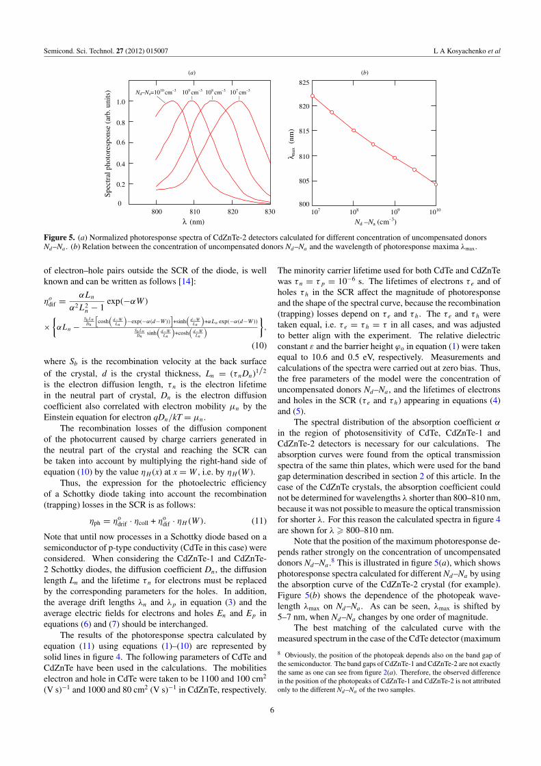
Figure 5. (a) Normalized photoresponse spectra of CdZnTe-2 detectors calculated for different concentration of uncompensated donorsNd–Na . (b) Relation between the concentration of uncompensated donors Nd–Na and the wavelength of photoresponse maxima λmax.
of electron–hole pairs outside the SCR of the diode, is wellknown and can be written as follows [14]:
ηodif = αLn
α2L2n − 1
exp(−αW)
×{αLn −
SbLnDn
[cosh
(d−WLn
)−exp(−α(d−W))
]+sinh
(d−WLn
)+αLn exp(−α(d−W))
SbLnDn
sinh(
d−WLn
)+cosh
(d−WLn
)},
(10)
where Sb is the recombination velocity at the back surfaceof the crystal, d is the crystal thickness, Ln = (τnDn)1/2
is the electron diffusion length, τn is the electron lifetimein the neutral part of crystal, Dn is the electron diffusioncoefficient also correlated with electron mobility μn by theEinstein equation for electron qDn/kT = μn.
The recombination losses of the diffusion componentof the photocurrent caused by charge carriers generated inthe neutral part of the crystal and reaching the SCR canbe taken into account by multiplying the right-hand side ofequation (10) by the value ηH (x) at x = W , i.e. by ηH (W ).
Thus, the expression for the photoelectric efficiencyof a Schottky diode taking into account the recombination(trapping) losses in the SCR is as follows:
ηph = ηodrif · ηcoll + ηo
dif · ηH (W). (11)
Note that until now processes in a Schottky diode based on asemiconductor of p-type conductivity (CdTe in this case) wereconsidered. When considering the CdZnTe-1 and CdZnTe-2 Schottky diodes, the diffusion coefficient Dn, the diffusionlength Ln and the lifetime τn for electrons must be replacedby the corresponding parameters for the holes. In addition,the average drift lengths λn and λp in equation (3) and theaverage electric fields for electrons and holes En and Ep inequations (6) and (7) should be interchanged.
The results of the photoresponse spectra calculated byequation (11) using equations (1)–(10) are represented bysolid lines in figure 4. The following parameters of CdTe andCdZnTe have been used in the calculations. The mobilitieselectron and hole in CdTe were taken to be 1100 and 100 cm2
(V s)−1 and 1000 and 80 cm2 (V s)−1 in CdZnTe, respectively.
The minority carrier lifetime used for both CdTe and CdZnTewas τn = τp = 10−6 s. The lifetimes of electrons τ e and ofholes τh in the SCR affect the magnitude of photoresponseand the shape of the spectral curve, because the recombination(trapping) losses depend on τ e and τh. The τ e and τh weretaken equal, i.e. τ e = τh = τ in all cases, and was adjustedto better align with the experiment. The relative dielectricconstant ε and the barrier height ϕo in equation (1) were takenequal to 10.6 and 0.5 eV, respectively. Measurements andcalculations of the spectra were carried out at zero bias. Thus,the free parameters of the model were the concentration ofuncompensated donors Nd–Na , and the lifetimes of electronsand holes in the SCR (τ e and τh) appearing in equations (4)and (5).
The spectral distribution of the absorption coefficient α
in the region of photosensitivity of CdTe, CdZnTe-1 andCdZnTe-2 detectors is necessary for our calculations. Theabsorption curves were found from the optical transmissionspectra of the same thin plates, which were used for the bandgap determination described in section 2 of this article. In thecase of the CdZnTe crystals, the absorption coefficient couldnot be determined for wavelengths λ shorter than 800–810 nm,because it was not possible to measure the optical transmissionfor shorter λ. For this reason the calculated spectra in figure 4are shown for λ � 800–810 nm.
Note that the position of the maximum photoresponse de-pends rather strongly on the concentration of uncompensateddonors Nd–Na .8 This is illustrated in figure 5(a), which showsphotoresponse spectra calculated for different Nd–Na by usingthe absorption curve of the CdZnTe-2 crystal (for example).Figure 5(b) shows the dependence of the photopeak wave-length λmax on Nd–Na . As can be seen, λmax is shifted by5–7 nm, when Nd–Na changes by one order of magnitude.
The best matching of the calculated curve with themeasured spectrum in the case of the CdTe detector (maximum
8 Obviously, the position of the photopeak depends also on the band gap ofthe semiconductor. The band gaps of CdZnTe-1 and CdZnTe-2 are not exactlythe same as one can see from figure 2(a). Therefore, the observed differencein the position of the photopeaks of CdZnTe-1 and CdZnTe-2 is not attributedonly to the different Nd–Na of the two samples.
6
Semicond. Sci. Technol. 27 (2012) 015007 L A Kosyachenko et al
at 850 nm) was achieved for Nd–Na = (1.5–2) × 1012 cm−3
and for lifetimes of electrons and holes in the SCR τ e = τh
= τ = 5 × 10⁻⁹ s. As one can see from figure 4(a), theresults of the calculation (solid line) agree quite well withmeasurements (circles). This can be interpreted as strongevidence of the theoretical model describing the underlyingphysical phenomena adequately.
For the CdZnTe-2 detector (figure 4(b)), the maximum onthe spectral photoresponse is shifted to a shorter wavelength(816 nm) due to the fact that the CdZnTe band gap is widerthan the CdTe one. The best fit between measurement andcalculation results is obtained for Nd–Na = 2 × 108 cm−3
and τ e = τh = τ ≈ 10−8 s, i.e. we observe that Nd–Na isfour orders of magnitude lower than in the CdTe detector.This difference corresponds to a difference of two orders ofmagnitude of the SCR width W . It seems improbable thatsuch a significant difference in the Nd–Na value and hence inW is the result of measurement errors, because the maximumof the calculated photoresponse curve is shifted markedlyfrom the experimental peak, if the value Nd–Na decreasesor increases by 30–40%. Thus, the results of the photoelectricstudies reveal a significant difference of the concentration ofuncompensated impurities between a highly efficient CdTeSchottky detector and a CdZnTe one, which is practically notsensitive to the radiation of the isotopes used.
Figure 4(c) shows the comparison of the calculatedspectrum with the measured photoresponse for the CdZnTe-1detector, which registers x/γ -ray spectra, but with anefficiency inferior from that of the CdTe detector. In this case,good agreement between calculated and measured spectra isobtained for Nd–Na = (8–10) × 108 cm−3 and for τ e = τh =τ = 10−8 s. This Nd–Na value is located at an intermediateposition between the Nd–Na values of the CdTe and CdZnTe-2detectors. It turns out that the increase of the concentrationof the uncompensated donors by 5–6 times compared to theCdZnTe-2 detector is already sufficient to record the radiationof isotopes used.
The study of the photoresponse spectra of the CdTe,CdZnTe-1 and CdZnTe-2 Schottky diodes allows us to suggestthat detection efficiency decreases when the concentration ofuncompensated impurities reduces from ∼1012 to ∼109 cm−3
and further to ∼108 cm−3. This suggestion is confirmed by thecalculations presented in section 5, while the correctness of theclassification of the samples with respect to their concentrationof uncompensated impurities is also confirmed by the studypresented in the next section 4.
4. Compensation degree of impurities in CdTe andCd0.9Zn0.1Te crystals
In this section we present an analysis of the compensationdegree of the materials based on the resistivity measurementsof the samples. This analysis verifies independently the resultsof the previous section, at least qualitatively. The observedlow concentrations of uncompensated impurities (108–1012
cm−3) obviously indicate a high degree of compensation ofthe semiconductors, which is the result of the doping of theCdTe and CdZnTe crystals with Cl or In accompanied by
the formation of self-compensating complexes (associates) aspredicted by the theory [4, 5].
When the dopant concentration of Cl or In is so high thatit has the dominant influence on the electrical conductivity, theanalytical treatment of the charge carrier statistics is reduced tothe solution of the electroneutrality equation in the simplifiedform:
n + N−a = p + N+
d , (12)
where n and p are the concentrations of electrons and holes inthe conduction band and valence bands, and N−
a and N+d are the
concentrations of charged acceptors and donors, respectively.Furthermore, when equation (12) is used to find the
Fermi level, the free carrier concentrations n and p can beneglected, because they are orders of magnitude lower thanthe concentrations of the donors and acceptors in the semi-insulating crystal. Another reasonable assumption is that thelevels of the compensating acceptors are located in a lowerhalf of the band gap, that is they are fully ionized and we canassume N−
a ≈ Na .Finally, it should be borne in mind that part of the
intentionally introduced shallow donors (Cl, In) remainunbound to complexes and manifest themselves as shallowdonors, i.e. we are dealing with a ‘standard’ three-levelcompensation model [15]. At a high compensation degreeξ = Na/Nd the concentration of shallow donors (1–ξ ) · Nd ismuch lower than the concentration of bound donors ξ · Nd.Therefore, the concentration of shallow donors can also beignored in the electroneutrality equation, which is assumed inequation (12).
With the above simplifications, equation (12) reduces tothe expression
Nd
exp(
�μ−Ed
kT
)+ 1
= Na, (13)
whose analytical solution for �μ is
�μcalc(T ) = Ed + kT ln
(1 − ξ
ξ
), (14)
where the Fermi level energy is measured from the top of thevalence band.9
We have verified that the value of the Fermi levelenergy found by taking into account the concentration of theunbounded shallow donors (Cl, In) to complexes (as well asthe electrons in the conduction band and of the holes in thevalence band) practically coincides with the Fermi level energyfound by ignoring them. This means that equations (13) and(14) are reasonably accurate.
Our method for the determination of the compensationdegree of the material is based on the fit of �μcalc(T) calculatedby equation (14) to �μρ(T) extracted from the temperaturedependence of the resistivity ρ(T) shown in figure 2(b).
In the case of a semiconductor with almost intrinsicconduction, carriers of both signs should be consideredin the expression for the resistivity: ρ(�μρ) =9 Taking into account the degeneracy factor in equation (13) has little effecton the final results of calculations.
7
Semicond. Sci. Technol. 27 (2012) 015007 L A Kosyachenko et al
280 300 320 340 3600.65
0.70
0.75
0.80
0.85
1000/T
Δ μρ,
Δμ i
, Δμ c
alc (
eV)
CdZnTe-1
CdZnTe-2CdTe
Δμ i
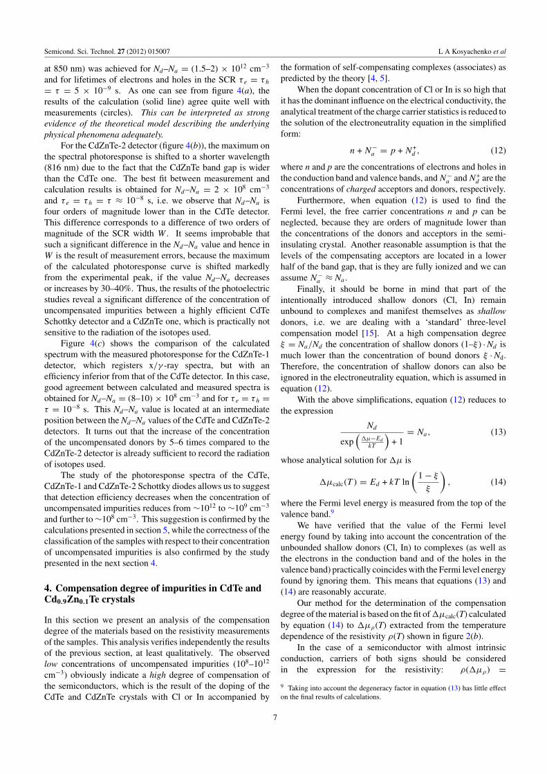
Figure 6. Temperature dependence of the Fermi level energy of theCdTe, CdZnTe-1 and CdZnTe-2 crystals. Circles, triangles andsquares show the values of �μρ(T) extracted from experimentaldata by using equation (15). Solid lines show �μcalc(T) calculatedwith equation (14) while dashed lines show �μi(T), the Fermilevels in the intrinsic materials.
Table 1. Parameters of crystals under study.
Material Nd–Na (cm−3) Ed (eV) ξ = Na/Nd
CdTe (1.5–2) × 1012 0.783 0.976CdZnTe-1 (1–1.2) × 109 0.957 0.995CdZnTe-2 2 × 10⁸ 1.095 0.999 98
1/(qn(�μρ)μn+qp(�μρ)μp). The solution of this equationfor �μρ will have the form
�μρ = kT ln
⎛⎝1 ±
√1 − 4q2ρ2μnμpn2
i
2qρμpn2i /Nv
⎞⎠ , (15)
where ‘+’ and ‘–’ correspond to the electron and holeconductivity of the semiconductor, ni is the intrinsic carrierconcentration and Nv is the effective density of states in thevalence band.
Figure 6 shows the temperature dependence of theFermi level energies �μρ(T) and �μcalc(T) extracted fromexperimental data by using equation (15) and calculatedwith equation (14) for the CdTe, CdZnTe-1 and CdZnTe-2crystals.
The results of the calculation of �μcalc(T) by equation (14)(solid lines in figure 6) are obtained by choosing the values ofEd and ξ , which fit in the best way to �μρ(T) obtained fromthe resistivity measurements. It should be emphasized that thevalue of ξ determines the slope of the line and the value of Ed
displaces the line along the vertical axis, i.e. the best fit betweentheory and experiment is a single combination of Ed and ξ .The resulting values of Ed and ξ for the three crystals studiedare summarized in table 1 together with the concentrations ofuncompensated impurities found in the previous section.
It turns out that the CdTe crystal doped with Cl and theCdZnTe crystals doped with In are characterized by a high
degree of compensation (from 97.6% to 99.998%). Thus, theresults presented are the experimental confirmation of the self-compensation model of the impurity complexes responsiblefor the electrical conductivity of CdTe and CdZnTe crystals,which was grounded theoretically by Mandel and Moreheadin the 1960s [4, 5].
It is clear from the results of the fit that the degree ofcompensation in CdZnTe-2 (0.999 98) is much higher thanin CdTe (0.976), i.e. the concentration of uncompensateddonors in CdZnTe is much lower than in CdTe. The degreeof compensation in CdZnTe-1 (0.995) has an intermediateposition exceeding the degree of compensation in CdTe. Thismeans that the classification of the crystals according to theirdegree of compensation found using the resistivity data is thesame with the classification according to their concentrationof uncompensated impurities found from the photoresponsedata.
The data presented in table 1 explain how the three crystalswith such different values of Ed and ξ have resistivity valuesclose to each other. In the CdTe crystal, the compensateddonor level is located in the upper half of the band gap(Ed = 0.783 eV). When the compensation degree ξ = 0.5, theFermi level coincides with the donor level, and at ξ = 0.976 itdrops to the level of 0.69 eV providing the p-type conductivity,which is close to the intrinsic conductivity of the material. Inthe CdZnTe-1 crystal, the donor level is located considerablyhigher (0.957 eV). With a higher degree of compensation ofξ = 0.995 the Fermi level is lowered to the level of 0.82 eV alsoproviding the almost intrinsic conductivity. It is located abovemid-gap and proves the n-type conductivity of the material. Inthe CdZnTe-2 crystal, the donor level is located even higher(Ed = 1.095 eV) and at a higher degree of compensation(ξ = 0.999 98), the Fermi level falls at 300 K to 0.81 eV,providing the n-type conductivity of the material. However,at temperatures above 330 K, the Fermi level drops below theFermi level of the intrinsic semiconductor, which means thatthe conduction of the material becomes p-type.10
It should be noted that quantitative agreement betweenthe calculation results of the compensation degree and ofthe concentration of uncompensated impurities may not beachieved. Indeed, the Fermi level and consequently theresistivity of the crystal are determined by the energy positionand the compensation degree of the center responsible for theelectrical conductivity of the material. In contrast, the width ofthe SCR in the Schottky diode is determined in accordance withthe Poisson equation by the density of space charge createdby all donors and all acceptors, i.e. by total concentrations ofuncompensated impurities.
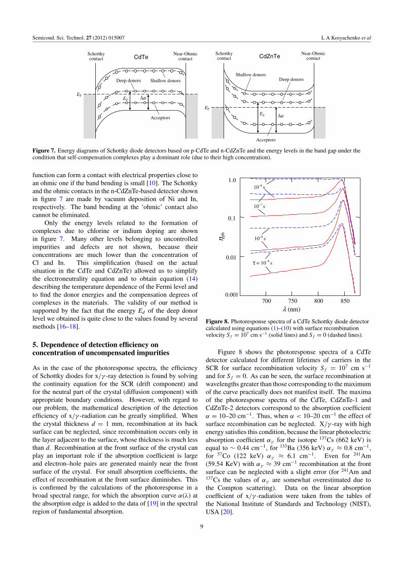
Figure 7 shows the energy diagram of the CdTe andCdZnTe detectors (at room temperature for CdZnTe). Thelevels of the deep and shallow donors and of the acceptors areindicated.
The CdTe detector is a Ni/CdTe/Ni structure. By varyingtechnological conditions, it is possible to change band bendingat the interface of a p-CdTe crystal with Ni, and hence tomodify properties of the contact. A metal with a high work
10 Apparently, this has a catastrophic impact on either a detector with ohmiccontacts or with a Schottky contact when the operating temperature changes.
8
Semicond. Sci. Technol. 27 (2012) 015007 L A Kosyachenko et al
Ed Δμ
Acceptors
Deep donors
EF
CdTe Schottky contact
Near-Ohmic contact
Shallow donors
Ed Δμ
EF
CdZnTe Schottky contact
Near-Ohmic contact
Acceptors
Deep donors Shallow donors
Figure 7. Energy diagrams of Schottky diode detectors based on p-CdTe and n-CdZnTe and the energy levels in the band gap under thecondition that self-compensation complexes play a dominant role (due to their high concentration).
function can form a contact with electrical properties close toan ohmic one if the band bending is small [10]. The Schottkyand the ohmic contacts in the n-CdZnTe-based detector shownin figure 7 are made by vacuum deposition of Ni and In,respectively. The band bending at the ‘ohmic’ contact alsocannot be eliminated.
Only the energy levels related to the formation ofcomplexes due to chlorine or indium doping are shownin figure 7. Many other levels belonging to uncontrolledimpurities and defects are not shown, because theirconcentrations are much lower than the concentration ofCl and In. This simplification (based on the actualsituation in the CdTe and CdZnTe) allowed us to simplifythe electroneutrality equation and to obtain equation (14)describing the temperature dependence of the Fermi level andto find the donor energies and the compensation degrees ofcomplexes in the materials. The validity of our method issupported by the fact that the energy Ed of the deep donorlevel we obtained is quite close to the values found by severalmethods [16–18].
5. Dependence of detection efficiency onconcentration of uncompensated impurities
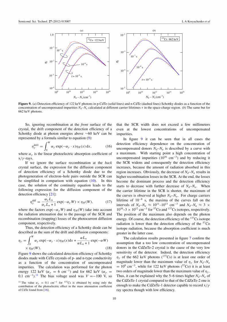
As in the case of the photoresponse spectra, the efficiencyof Schottky diodes for x/γ -ray detection is found by solvingthe continuity equation for the SCR (drift component) andfor the neutral part of the crystal (diffusion component) withappropriate boundary conditions. However, with regard toour problem, the mathematical description of the detectionefficiency of x/γ -radiation can be greatly simplified. Whenthe crystal thickness d = 1 mm, recombination at its backsurface can be neglected, since recombination occurs only inthe layer adjacent to the surface, whose thickness is much lessthan d. Recombination at the front surface of the crystal canplay an important role if the absorption coefficient is largeand electron–hole pairs are generated mainly near the frontsurface of the crystal. For small absorption coefficients, theeffect of recombination at the front surface diminishes. Thisis confirmed by the calculations of the photoresponse in abroad spectral range, for which the absorption curve α(λ) atthe absorption edge is added to the data of [19] in the spectralregion of fundamental absorption.
λ (nm)700 750 800 850
0.01
0.1
1.0
0.001
10–6 s
10–7 s
10–8 s
τ = 10–9 s
η ph
Figure 8. Photoresponse spectra of a CdTe Schottky diode detectorcalculated using equations (1)–(10) with surface recombinationvelocity Sf = 107 cm s−1 (solid lines) and Sf = 0 (dashed lines).
Figure 8 shows the photoresponse spectra of a CdTedetector calculated for different lifetimes of carriers in theSCR for surface recombination velocity Sf = 107 cm s−1
and for Sf = 0. As can be seen, the surface recombination atwavelengths greater than those corresponding to the maximumof the curve practically does not manifest itself. The maximaof the photoresponse spectra of the CdTe, CdZnTe-1 andCdZnTe-2 detectors correspond to the absorption coefficientα = 10–20 cm−1. Thus, when α < 10–20 cm−1 the effect ofsurface recombination can be neglected. X/γ -ray with highenergy satisfies this condition, because the linear photoelectricabsorption coefficient αγ for the isotope 137Cs (662 keV) isequal to ∼ 0.44 cm−1, for 133Ba (356 keV) αγ ≈ 0.8 cm−1,for 57Co (122 keV) αγ ≈ 6.1 cm−1. Even for 241Am(59.54 KeV) with αγ ≈ 39 cm−1 recombination at the frontsurface can be neglected with a slight error (for 241Am and137Cs the values of αγ are somewhat overestimated due tothe Compton scattering). Data on the linear absorptioncoefficient of x/γ -radiation were taken from the tables ofthe National Institute of Standards and Technology (NIST),USA [20].
9
Semicond. Sci. Technol. 27 (2012) 015007 L A Kosyachenko et al
10–7 s
57Co 122 keV
108 1010 1012 1014 1016
1.0
10–3
10–2
10–4
Nd – Na (cm–3)
η γ
(a)
τ = 10–9 s
10–8 s
10–1
108 1010 1012 1014 1016
10–2
10–3
10–4
10–5
Nd – Na (cm–3)
η γ
τ = 10–9 s
10–7 s
10–8 s
137Cs 662 keV
(b)
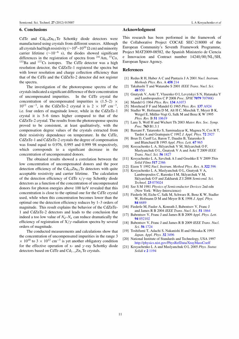
Figure 9. (a) Detection efficiency of 122 keV photons in p-CdTe (solid lines) and n-CdTe (dashed lines) Schottky diodes as a function of theconcentration of uncompensated impurities Nd–Na calculated at different carrier lifetimes τ in the space-charge region. (b) The same but for662 keV photons.
So, ignoring recombination at the front surface of thecrystal, the drift component of the detection efficiency of aSchottky diode at photon energies above ∼60 keV can berepresented by a formula similar to equation (9):
ηdriftγ =
∫ W
0αγ exp(−αγ · x)ηH (x) dx, (16)
where αγ is the linear photoelectric absorption coefficient ofx/γ -rays.
If we ignore the surface recombination at the backcrystal surface, the expression for the diffusion componentof detection efficiency of a Schottky diode due to thephotogeneration of electron–hole pairs outside the SCR canbe simplified in comparison with equation (10). In thiscase, the solution of the continuity equation leads to thefollowing expression for the diffusion component of thedetection efficiency [21]:
ηdiffγ = αγ Ln
αγ Ln + 1exp(−αγ W) × ηH (W), (17)
where the factors exp(−αγ W ) and ηH (W ) take into accountthe radiation attenuation due to the passage of the SCR andrecombination (trapping) losses of the photocurrent diffusioncomponent, respectively.
Thus, the detection efficiency of a Schottky diode can bedescribed as the sum of the drift and diffusion components:
ηγ =∫ W
0αγ exp(−αγ · x)ηH (x)dx +
αLn
αLn + 1exp(−αW)
× ηH (W). (18)
Figure 9 shows the calculated detection efficiency of Schottkydiodes made with CdTe crystals of p- and n-type conductivityas a function of the concentration of uncompensatedimpurities. The calculation was performed for the photonenergy 122 keV (αγ = 6 cm−1) and for 662 keV (αγ =0.1 cm−1).11 The bias voltage used was V =−100 V, so11 The value αγ = 0.1 cm−1 for 137Cs is obtained by using only thecontribution of the photoelectric effect in the mass attenuation coefficientof CdTe found from [16].
that the SCR width does not exceed a few millimeterseven at the lowest concentrations of uncompensatedimpurities.
In figure 9 it can be seen that in all cases thedetection efficiency dependence on the concentration ofuncompensated donors Nd–Na is described by a curve witha maximum. With starting point a high concentration ofuncompensated impurities (1016 cm−3) and by reducing itthe SCR widens and consequently the detection efficiencyincreases, because the amount of radiation absorbed in thisregion increases. Obviously, the decrease of Nd–Na results inhigher recombination losses in the SCR. At the end, the lossesbecome the dominant process and the detection efficiencystarts to decrease with further decrease of Nd–Na . Whenthe carrier lifetime in the SCR is shorter, the maximum ofthe curves is observed at higher Nd–Na . For charge carrierslifetime of 10−8 s, the maxima of the curves fall on theintervals of Nd–Na ≈ 1011–1013 cm−3 and Nd–Na ≈ 3 ×10¹⁰–3 × 1012 cm−3 for 57Co and 137Cs isotopes, respectively.The position of the maximum also depends on the photonenergy. Of course, the detection efficiency of the 137Cs isotoperadiation is lower than the detection efficiency of the 57Coisotope radiation, because the absorption coefficient is muchgreater in the latter case.
The calculation results presented in figure 7 confirm theassumption that a too low concentration of uncompensateddonors in the CdZnTe-2 crystal is the cause of the very lowsensitivity of the detector. Indeed, the detection efficiencyηγ of the 662 keV photons (137Cs) is at least one order ofmagnitude lower than the maximum value of ηγ for Nd–Na
= 109 cm−3, while for 122 keV photons (57Co) it is at leasttwo orders of magnitude lower than the maximum value of ηγ .Thus, it can be explained why the 5–6 times higher Nd–Na ofthe CdZnTe-1 crystal compared to that of the CdZnTe-2 one isenough to make the CdZnTe-1 detector capable to record x/γ
ray spectra though with low efficiency.
10
Semicond. Sci. Technol. 27 (2012) 015007 L A Kosyachenko et al
6. Conclusions
CdTe and Cd0.9Zn0.1Te Schottky diode detectors weremanufactured using crystals from different sources. Althoughall crystals had high resistivity (∼109–1010 � cm) and minoritycarrier lifetime (∼10−6 s), the diodes showed significantdifferences in the registration of spectra from 241Am, 57Co,133Ba and 137Cs isotopes. The CdTe detector was a highresolution detector, the CdZnTe-1 registered the spectra butwith lower resolution and charge collection efficiency thanthat of the CdTe and the CdZnTe-2 detector did not registerthe spectra.
The investigation of the photoresponse spectra of thecrystals indicated a significant difference of their concentrationof uncompensated impurities. In the CdTe crystal theconcentration of uncompensated impurities is (1.5–2) ×1012 cm−3, in the CdZnTe-2 crystal it is 2 × 108 cm−3,i.e. four orders of magnitude lower, while in the CdZnTe-1crystal it is 5–6 times higher compared to that of theCdZnTe-2 crystal. The results from the photoresponse spectraproved to be consistent, at least qualitatively, with thecompensation degree values of the crystals extracted fromtheir resistivity dependence on temperature. In the CdTe,CdZnTe-1 and CdZnTe-2 crystals the degree of compensationwas found equal to 0.976, 0.995 and 0.999 98 respectively,which corresponds to a significant decrease in theconcentration of uncompensated donors.
The obtained results showed a correlation between thelow concentration of uncompensated donors and the poordetection efficiency of the Cd0.9Zn0.1Te detectors with quiteacceptable resistivity and carrier lifetime. The calculationof the detection efficiency of CdTe x/γ -ray Schottky diodedetectors as a function of the concentration of uncompensateddonors for photon energies above 100 keV revealed that thisconcentration is close to the optimal one for the CdTe crystalused, while when this concentration becomes lower than theoptimal one the detection efficiency reduces by 1–3 orders ofmagnitude. This result explains the behavior of the CdZnTe-1 and CdZnTe-2 detectors and leads to the conclusion thatindeed a too low value of Nd–Na can reduce dramatically theefficiency of registration of X/γ -radiation spectra by severalorders of magnitude.
The conducted measurements and calculations show thatthe concentration of uncompensated impurities in the range 3× 10¹⁰ to 3 × 1012 cm−3 is yet another obligatory conditionfor the effective operation of x- and γ -ray Schottky diodedetectors based on CdTe and Cd1−xZnxTe crystals.
Acknowledgment
This research has been performed in the framework ofthe Collaborative Project COCAE SEC-218000 of theEuropean Community’s Seventh Framework Programme,Project MAT2009-08582, the Spanish Ministerio de Cienciae Innovacion and Contract number 14240/00/NL/SH,European Space Agency.
References
[1] Redus R H, Huber A C and Pantazis J A 2001 Nucl. Instrum.Methods Phys. Res. A 458 214
[2] Takahashi T and Watanabe S 2001 IEEE Trans. Nucl. Sci.48 950
[3] Gnatyuk V, Aoki T, Vlasenko O I, Levytskyi S N, Hatanaka Yand Lambropoulos C P 2008 Proc. SPIE 7079 70790G
[4] Mandel G 1964 Phys. Rev. 134 A1073[5] Morehead F F and Mandel G 1965 Phys. Rev. 137 A924[6] Stadler W, Hofmann D M, Alt H C, Muschik T, Meyer B K,
Weigel E, Muller-Vogt G, Salk M and Benz K W 1995Phys. Rev. B 51 10619
[7] Lany S, Wolf H and Wichert Th 2003 Mater. Res. Soc. Symp.Proc. 763 B1.3.1
[8] Bassani F, Tatarenko S, Saminadayar K, Magnea N, Cox R T,Tardot A and Grattepain C 1992 J. Appl. Phys. 72 2927
[9] Brun D, Cunff Le, Baron T, Daudin B, Tatarenko Sand Blanchard B 1995 Appl. Phys. Lett. 67 965
[10] Kosyachenko L A, Sklyarchuk V M, Sklyarchuk O F,Maslyanchuk O L, Gnatyuk V A and Aoki T 2009 IEEETrans. Nucl. Sci. 56 1827
[11] Kosyachenko L A, Savchuk A I and Grushko E V 2009 ThinSolid Films 517 2386
[12] Eizen Y 1992 Nucl. Instrum. Method Phys. Res. A 322 596[13] Kosyachenko L A, Maslyanchuk O L, Gnatyuk V A,
Lambropoulos C, Rarenko I M, Sklyarchuk V M,Sklyarchuk O F and Zakharuk Z I 2008 Semicond. Sci.Technol. 23 075024
[14] Sze S M 1981 Physics of Semiconductor Devices 2nd edn(New York: Wiley-Interscience)
[15] Fiederle M, Eiche C, Salk M, Schwarz R, Benz K W, StadlerW, Hofmann D M and Meyer B K 1998 J. Appl. Phys.84 6689
[16] Fiederle M, Fauler A, Konrath J, Babentsov V, Franc Jand James R B 2004 IEEE Trans. Nucl. Sci. 51 1864
[17] Babentsov V, Franc J and James R B 2009 Appl. Phys. Lett.94 052102
[18] Babentsov V, Franc J and James R B 2009 IEEE Trans. Nucl.Sci. 56 1724
[19] Toshifumi T, Adachi S, Nakanishi H and Ohtsuka K 1993Japan. Appl. Phys. 32 3496
[20] National Institute of Standards and Technology, USA 1997http://physics.nist.gov/PhysRefData/XrayMassCoeff
[21] Kosyachenko L A and Maslyanchuk O L 2005 Phys. StatusSolidi c 2 1194
11


![Elastic response of [111]-tunnelling impurities](https://img.pdfslide.net/doc/110x75/6344c9f138eecfb33a063ffe/elastic-response-of-111-tunnelling-impurities.jpg)


