Embed Size (px)
Citation preview

1
Selective compensation of voltage harmonics in grid-connected microgrids
Mehdi Savaghebi
a, Juan C. Vasquez b, Alireza Jalilian
a, Josep M. Guerrero b, Tzung-Lin Lee
c
Emails: [email protected], [email protected], [email protected], [email protected], [email protected]
a Center of excellence for power system automation and operation, Electrical engineering department, Iran University of science and technology, Tehran 16846-13114, Iran
b Institute of energy technology, Aalborg University, Aalborg east DK-9220, Denmark
c Department of electrical engineering, National Sun Yat-sen University, Kaohsiung 80424, Taiwan
Corresponding author:
Mehdi Savaghebi
Email: [email protected] , [email protected]
Tel: (+98) 937 458 1790
Fax: (+98) 21 73225777
Address: Electrical engineering department, Iran University of science and technology, Tehran 16846-13114, Iran

2
Abstract
In this paper, a novel approach is proposed for selective compensation of main voltage harmonics in a grid-connected microgrid. The aim of compensation is to provide a high voltage quality at the point of common coupling (PCC). PCC voltage quality is of great importance due to sensitive loads that may be connected. It is assumed that the voltage harmonics are originated from distortion in grid voltage as well as the harmonic current of the nonlinear loads. Harmonic compensation is achieved through proper control of distributed generators (DGs) interface converters. The compensation effort of each harmonic is shared considering the respective current harmonic supplied by the DGs. The control system of each DG comprises harmonic compensator, fundamental power controllers, voltage and current proportional-resonant controller and virtual impedance loop. Virtual impedance is considered at fundamental frequency to enhance power control and also at harmonic frequencies to improve the nonlinear load sharing among DGs. The control system design is discussed in detail. The presented simulation results demonstrate the effectiveness of the proposed method in compensation of the voltage harmonics to an acceptable level.
Keywords
Distributed Generator (DG); microgrid; grid-connected; voltage harmonics compensation.
1. Introduction
The proliferation of different nonlinear loads in electrical systems has resulted in the voltage harmonic distortion. This distortion can cause variety of problems such as protective relays malfunction, overheating of motors and transformers and failure of power factor correction capacitors [10, 27]. Thus, in different standards some limits are recommended for voltage harmonics, e.g. IEEE Standard 519-1992 [18].
On the other hand, it is well-known that the Distributed Generators (DGs) often consist of a prime mover connected through a power-electronic interface converter to the utility grid or microgrid. Microgrid is a local grid consisting of DGs, energy storage systems and dispersed loads which may operate in both grid-connected and islanded modes [20].
The main role of an interface converter is to control active power injection. However, compensation of power quality problems, such as voltage harmonics can be achieved through proper control strategies. A single-phase DG capable of improving voltage waveform is presented in [9]. DG is controlled to operate as a shunt active power filter. In other words, DG injects harmonic current to improve voltage waveform.
The voltage harmonic compensation methods of [17, 30, 31, 34] are based on making the DG emulate a resistance at harmonic frequencies. The idea of resistance emulation is originally proposed in [2] for active power filters.
A method for compensation of voltage harmonics in an islanded microgrid has been presented in [24]. This method is also based on the resistance emulation. Furthermore, a droop characteristic based on the DG harmonic reactive power has been considered to achieve sharing of the harmonic compensation effort. That was the first approach toward cooperative control of DGs to compensate voltage harmonics. A similar approach applicable to both grid-connected and islanded operating modes of microgrid is proposed in [33].
It is well known for the active power filters that the selective compensation of harmonics can provide some advantages in terms of filter rating and control robustness [23, 25, 28]. Similarly, it can be concluded that selective compensation methods are more appropriate in the case of harmonic compensation by DG units while the approaches of [24, 33] are based on compensating the voltage harmonics of a microgrid in a non-selective manner. Furthermore, the aforementioned harmonic compensation methods are designed for compensation of voltage harmonics at the DG terminal while usually the power quality at the point of common coupling (PCC) is

3
the main concern due to the sensitive loads that may be connected. In addition, if the DGs try to compensate the local voltage harmonics, the harmonic distortion may be amplified in some of the buses of electrical system. This phenomenon is called “whack-a-mole” [38]. Thus, by direct compensation of PCC voltage harmonics, good power quality can be guaranteed for the sensitive loads connected to PCC.
In this paper, a method is proposed for compensation of the PCC main voltage harmonics in a grid-connected microgrid. It is assumed that the harmonic distortion is caused by the nonlinear loads as well as grid voltage distortion. Compensation is performed selectively for the main voltage harmonic orders. Compensation effort of each harmonic is shared considering the respective current harmonic supplied by the DGs.
The rest of the paper is organized as follows. DG control system structure is explained in section 2. The details of power calculation and control, voltage and current controllers, virtual impedance loop and harmonic compensation method are presented in this section. Section 3 is dedicated to the control system design in order to select proper control parameters. Simulation results are presented in section 4.
2. Microgrid DGs control system
Fig. 1 shows the single-line diagram of a grid-connected microgrid consisting of electronically-interfaced DGs and dispersed linear and nonlinear loads which are connected to PCC through some tie lines. Microgrid is connected to the utility grid through a tie line (Zg) and a transformer with the equal impedance of Zt. As shown in Fig. 1, PCC voltage harmonics data are extracted by the measurement block and sent to all DGs. These data are applied by the DG control system to generate proper control signals. Compensation is performed for the main harmonics of PCC voltage; thus, it is only necessary to extract and send these harmonics data. In this paper, 5th and 7th harmonics are considered as the main voltage harmonic orders. Considering this fact that PCC can be far from DGs, low bandwidth communication (LBC) is applied for sending PCC voltage harmonic data. Low communication bandwidth is selected in order to avoid dependence on the high bandwidth availability which may endanger the system reliability. In order to ensure that LBC is sufficient, the transmitted data should consist of approximately dc signals. Hence, the PCC voltage harmonic components are extracted in dq (synchronous) reference frame and then transmitted to each DG controller. Afterwards, as shown in Fig. 2, harmonic voltages are transformed to αβ (stationary) reference frame and fed to “Selective Harmonic Compensator” block. The rotation angles of transformations are set to -5φ* and 7φ* for the 5th and 7th harmonics, respectively. φ* is the reference of DG voltage phase angle which is generated by the active power controller.
The details of PCC 5th and 7th harmonic extraction are depicted in the “Measurement Block” of Fig. 2. At first, the measured PCC voltage (vabc) is transformed to dq frames rotating at -5ω, and 7ω, respectively. ω is the system angular frequency estimated by a phase-locked loop (PLL) [22]. Afterwards, two second-order low pass filters (LPF) with 2Hz cut-off frequency are used to extract 5th and 7th harmonics ( 5
dqv and 7dqv , respectively).
Second-order filters are applied since the first-order ones were not able to provide acceptable performance. For instance, the performance of first- and second-order filters (both with 2Hz cut-off frequency) in extracting d-component of PCC voltage fifth harmonic ( 5
dv ) is compared in Fig. 3. As it can be seen, first-order one is not able to filter the oscillations, properly and thus cannot meet the requirement of low bandwidth communication. It should be emphasized that the harmonic compensation control signals are generated and applied locally by each DG controller without using any data communication. The detailed structure of each DG power stage and control system is shown in Fig. 2. The power stage consists of a dc link, an interface inverter and an LC filter. It is assumed that an approximately constant dc voltage (Vdc) is maintained at the dc link. The details about the control of dc link voltage for different distributed resources can be found in [4]. However, a feedforward loop can be included as shown in Fig. 2 in order to consider small Vdc variations in generation of the inverter gate signals by pulse width modulator (PWM).

4
Fig. 1. Structure and control system of a grid- connected microgrid.
Fig. 2. DG power stage and control system.
DG2
2Z
1Z
2Z
Dispersed Loads
abcv
1ZDG1
Controller
DG2
Controller
DGn
Controller
nZ
DG1
DGn
Linear Load
Nonlinear Load
Measurement
Block
Point of Common Coupling (PCC) Utility Grid
7dqv
gZ
Transformer
5dqv
Low
Ban
dwid
th C
omm
unic
atio
n (L
BC
)dqhv
tZ
Microgrid
refvαβ
*iαβPRCurrent
Controller
PRVoltage
Controller
Three-phase Sinusoidal Reference Generator
abcαβabcαβ abcαβ
Virtual Impedanceabc αβ
Fundamental Powers
Calculation
*E
oi αβovαβLi αβ
abcoiabcovLabci
*cv
+−+−
dcV
L
L
L
CC
DG Power StageC
5−
DG Terminal
DG Control System
Fundamental Powers
Controllers
dc L
ink
αβ dqαβ dq
7
PCC
ωabcv
7dqv
PLL
5dqv
5−7
LPF
LPF
Measurement Block
LBC
*φ
abcdq
abcdq
PWM
×÷feed
forw
ard
PQ
7dqv
5dqv
*P
*Q
SelectiveHarmonic
Compensator
*vαβ
oi α5vαβ
7vαβ
++ −+
αβ abc
Vv αβ

5
Fig. 3. d-component of PCC voltage fifth harmonic.
The DG control system is designed in αβ reference frame; thus, Clarke transformations are used to transform the variables between abc and αβ coordinates. As shown in Fig. 2, the reference of the DG output voltage in αβ frame ( *vαβ ) is provided by power controllers, virtual impedance loop and harmonic compensator. On the other
hand, instantaneous output voltage (abcov ) is measured and transformed to αβ frame ( ov
αβ). Then, according to
*vαβ and ovαβ
, the reference current ( *iαβ ) is generated. As seen in Fig. 2, LC filter inductor current is
transformed to αβ frame ( Li αβ) and controlled by the current controller. The output of the current controller is
transformed back to abc frame to provide three-phase voltage reference for PWM block. Finally, PWM controls the switching of the inverter based on this reference.
2.1. Fundamental powers calculation
As seen in Fig. 2, instantaneous output voltage and current in αβ frame ( ovαβ
and oi αβ, respectively) are used
for calculation of the fundamental powers.
Based on the instantaneous reactive power theory [1], the instantaneous values of active and reactive powers should be calculated using equations (1) and (2), respectively:
o o o op v i v iα α β β
= + (1)
o o o oq v i v iβ α α β
= − (2)
Each of the instantaneous powers consists of dc and ac (oscillatory) components. The dc components (average values of p and q) are fundamental active and reactive powers (P and Q, respectively) [29]. The oscillatory parts are generated by the harmonic and/or unbalance contents of the voltage and current. The dc components are extracted using two first-order low pass filters. The cut-off frequency of these filters is set to 2Hz.
2.2. Fundamental powers controllers
Assuming a mainly inductive electrical system, fundamental frequency three-phase active and reactive powers can be expressed by the following equations, respectively [12]:
3 sinE VPX
φ⋅≈ ⋅ (3)
2cos3 E V VQXφ⋅ −≈ ⋅ (4)
where X is the reactance between DG and electrical grid, E and V are the phase rms values of the DG inverter

6
output voltage and the grid voltage and φ represents the angle between E and V. Assuming that the phase angle of the grid voltage to be zero, φ will be equal to phase angle of the inverter voltage.
In practical applications, φ is normally small; thus, P and Q can be assumed decoupled (cos 1φ ≈ and sin )φ φ≈and be controlled by DG output voltage phase angle and amplitude, respectively [3, 12, 15]. According to this, the following characteristics are considered for DG output power control in a grid-connected microgrid [15, 26,
37]: * * *
0 ( ) ( )P Im P P m P P dtφ φ= + − + −∫ (5) * * *
0 ( ) ( )P IE E n Q Q n Q Q dt= + − + −∫ (6) where • P*: active power reference • Q*: reactive power reference • E*: phase voltage amplitude reference • φ*: phase angle reference • E0: rated phase voltage amplitude • φ0: rated phase angle ( 0 0dt tω ω= ⋅∫ ) • ω0: rated frequency • mP: active power proportional coefficient • mI: active power integral coefficient • nP: reactive power proportional coefficient • nI: reactive power integral coefficient
P* can be determined to coincide with the maximum power which is provided by the DG prime mover. For instance, in the case of photovoltaic (PV) generation, a maximum power point tracker (MPPT) is applied to set P* [36]. Alternatively, P* and Q* can be set by a centralized controller aiming the economic optimization of the microgrid [35].
2.3. Voltage and current controllers
Due to the difficulties of using proportional-integral (PI) controllers to track non-dc variables, proportional-resonant (PR) controllers are usually preferred in the stationary reference frame [5]. In this paper, PR voltage and current controllers are respectively as follow:
( )0221,5,7
2( )
2k k
k
rV cVV pV
k cV
k sG s k
s s k
ω
ω ω=
⋅ ⋅= +
+ ⋅ ⋅ + ⋅∑ (7)
( )0221,5,7
2( )
2k k
k
rI cII pI
k cI
k sG s k
s s k
ω
ω ω=
⋅ ⋅= +
+ ⋅ ⋅ + ⋅∑ (8)
where pVk ( pIk ) and rVkk ( rIkk ) are the proportional and kth harmonic (including fundamental component as
the first harmonic) resonant coefficients of the voltage (current) controller, respectively. cVkω and cIkω
represent the voltage and current controllers cut-off frequencies at kth harmonic, respectively.

7
2.4. Virtual impedance loop
It has been assumed for the control of fundamental powers that the system impedances are mainly inductive. Thus, the accuracy of the power control is affected by the output impedance of the DG units as well as the line impedances. By including virtual impedance at fundamental frequency, the phase and magnitude of the output impedance can be fixed at the desired values and the effect of the line impedances can be mitigated [12-15].
Virtual resistance makes the oscillations of the system more damped [14]. The damping can also be provided by a physical resistance at the expense of efficiency decrease due to ohmic losses. In contrast with a physical resistance, the virtual resistance has no power losses, since is provided by a control loop; thus, it is possible to implement it without decreasing the efficiency [15]. Also, virtual inductance is considered to make the DG output impedance more inductive in order to improve the decoupling of P and Q. Thus, the virtual impedance enhances the droop controllers performance and stability [12, 16].
Furthermore, the virtual impedance can provide additional features such as sharing of nonlinear (harmonic) load. Some methods for harmonic current sharing among parallel converters are presented in [6-8] and [11-14]. It is suggested in [6] to use each order of the harmonic current to produce a proportional voltage drop which is leading the current by 90°. In fact, a virtual output inductance is inserted at the harmonic frequencies. As an alternative approach, it is proposed in [7, 8] and [11-14] to make the converters generate a virtual output resistance at the harmonic frequencies. This idea is applied for nonlinear load sharing in the present paper.
A three-phase system can be modeled as two independent single-phase systems in αβ reference frame. Thus, the concept of virtual impedance can be demonstrated as Fig. 4 which shows the single-phase equivalent Thévenin circuit of an inverter with a virtual impedance loop [14]. Based on Fig. 4, the following equations can be extracted:
( ) ( ) ( ) ( ) ( )refo o ov s G s v s Z s i s= ⋅ − ⋅ (9)
( ) ( ) ( )vo oZ s Z s Z s′= + (10)
where vref (s), G(s) and Zo(s) are the reference voltage, control system closed-loop transfer function and output impedance, respectively. ( )Z so′ represents the inverter output impedance without virtual impedance Zv(s).
The basic structure of the virtual impedance for αβ frame is proposed in [16]. Here, this structure is extended as shown in Fig. 5 by including the harmonic virtual resistance. In this Fig., Rv and Lv are the fundamental frequency virtual resistance and inductance, respectively, and Rv,h is the virtual resistance at 5th and 7th harmonics as the main harmonic orders.
As seen in Figs. 2 and 5, αβ components of instantaneous output current ( oi αβ) are fed to virtual impedance
loop. Then, fundamental component ( 1oi αβ
) and 5th and 7th harmonic orders ( 5oi αβ
and 7oi αβ
) are extracted as
explained in [32] and applied to implement selective virtual impedance. Applying the approach of [32], fundamental and harmonic frequencies can be directly extracted in αβ frame. Finally, the output of virtual impedance loop ( Vv
αβ) is subtracted from voltage reference ( refv
αβ) in order to generate *vαβ .
Fig. 4. Equivalent circuit of an inverter
( )o si
( ) ( )refG s sv⋅
( )oZ s′ ( )vZ s
( )o sv
( )oZ s
( )V sv

8
Fig. 5. Block diagram of selective virtual impedance.
2.5. Selective harmonic compensator
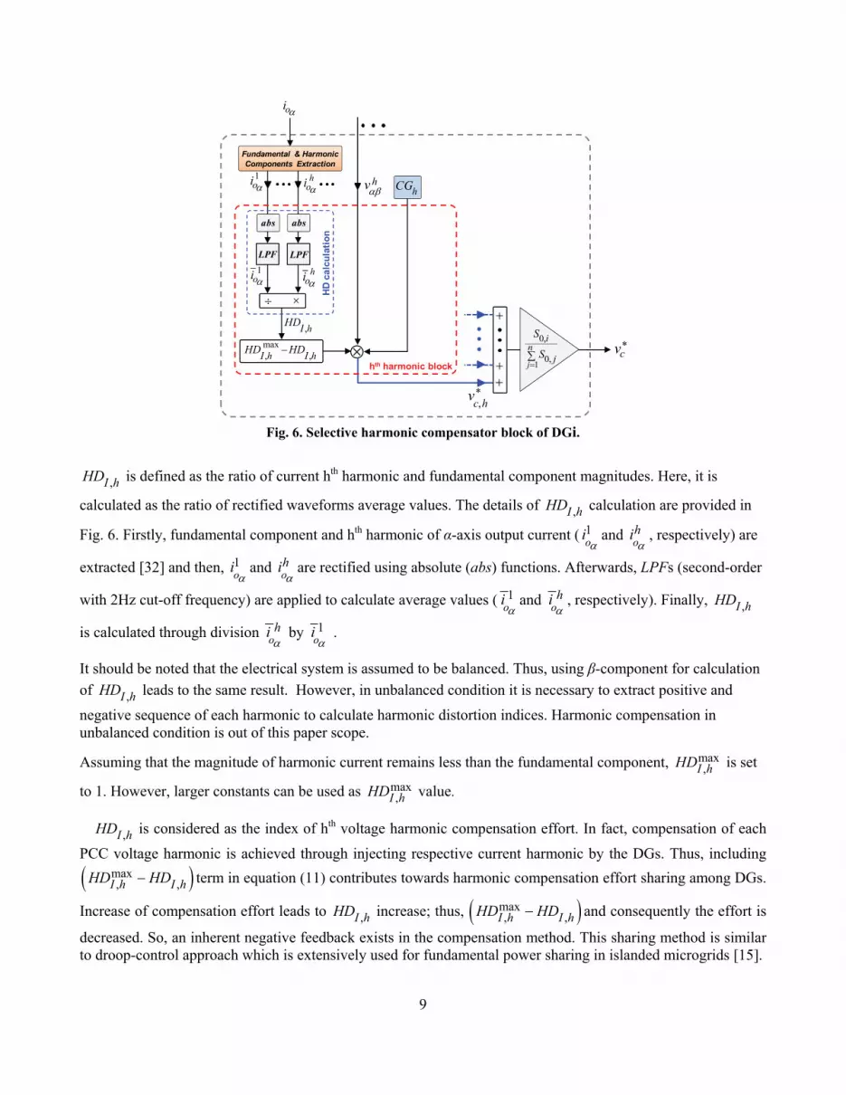
The details of “Selective Harmonic Compensator” block of Fig. 2 are presented in Fig. 6 for DG number i (DGi). As mentioned before, harmonic compensation is performed selectively for the main PCC voltage harmonics. Compensation reference of each harmonic ( *
,c hv for hth voltage harmonic) is generated separately
and then, all of the compensation references are added together. Afterwards, the resultant value is multiplied by
the ratio of DGi rated power (S0,i) and the total power of the microgrid DGs ( 0,1
nj
jS
=∑ ) to generate total
compensation reference ( *cv ) which is inserted as a voltage reference in the control system of Fig. 2. This way,
the compensation workload is distributed among microgrid DGs according to their rated powers.
According to Fig. 6, *,c hv
is generated as follows:
( )* max, , ,
hc h h I h I hv v CG HD HDαβ= ⋅ ⋅ − (11)
In equation (11), hvαβ is PCC voltage hth harmonic component in αβ frame and CGh is the compensation gain for
hth voltage harmonic. CGh is a negative constant which is the same for all DGs. CGh should be negative in order to generate a harmonic voltage with the polarity opposite of hvαβ and consequently cancel the PCC voltage
harmonic distortion. ,I hHD represents the current hth harmonic distortion index and max
,I hHD is the maximum
value of ,I hHD .
5 7o oi iα α+
1oi αβ
Fundamental and
Harmonic Components
Extraction5 7o oi iβ β+
⊕ Vv α
⊕ Vv βvR
vR
1oi β
1oi α
Fundamental Virtual Impedance
⊕
⊕
,v hR
,v hR
0vL ω−
oi αβ
0vL ω
9
Fig. 6. Selective harmonic compensator block of DGi.
,I hHD is defined as the ratio of current hth harmonic and fundamental component magnitudes. Here, it is
calculated as the ratio of rectified waveforms average values. The details of ,I hHD calculation are provided in
Fig. 6. Firstly, fundamental component and hth harmonic of α-axis output current ( 1oi α and o
hiα
, respectively) are
extracted [32] and then, 1oi α and o
hiα
are rectified using absolute (abs) functions. Afterwards, LPFs (second-order
with 2Hz cut-off frequency) are applied to calculate average values ( 1oi α and o
hiα
, respectively). Finally, ,I hHD
is calculated through division o
hiα
by 1oi α .
It should be noted that the electrical system is assumed to be balanced. Thus, using β-component for calculation of ,I hHD leads to the same result. However, in unbalanced condition it is necessary to extract positive and
negative sequence of each harmonic to calculate harmonic distortion indices. Harmonic compensation in unbalanced condition is out of this paper scope.
Assuming that the magnitude of harmonic current remains less than the fundamental component, max,I hHD
is set
to 1. However, larger constants can be used as max,I hHD value.
,I hHD is considered as the index of hth voltage harmonic compensation effort. In fact, compensation of each
PCC voltage harmonic is achieved through injecting respective current harmonic by the DGs. Thus, including
( )max, ,I h I hHD HD− term in equation (11) contributes towards harmonic compensation effort sharing among DGs.
Increase of compensation effort leads to ,I hHD increase; thus, ( )max
, ,I h I hHD HD− and consequently the effort is
decreased. So, an inherent negative feedback exists in the compensation method. This sharing method is similar to droop-control approach which is extensively used for fundamental power sharing in islanded microgrids [15].
hCGhvαβh
oi α1oi α
oi α
Fundamental & Harmonic Components Extraction
÷ ×
,hIHD
max, ,h hI IHD HD− ⊗
*,c hv
hth harmonic block
++
+
*cv
abs abs
LPFLPF
hoi α
1oi α
HD
cal
cula
tion
1
0
0
,
,j
ni
j
S
S=∑

10
A similar sharing idea has been presented in [24] using a droop characteristic based on the DG harmonic reactive power (H). But, calculation of H requires extracting the rms values of oscillatory parts of instantaneous powers calculated by equations (1) and (2). This kind of rms calculation needs a high computational effort and convergence time due to broad harmonic spectrum.
3. Control system design
3.1. Power controllers
A small signal analysis similar to what has been performed in [14] is applied as follows in order to select the parameters of power controllers. Equations (3) and (4) can be linearized as follows:
( )ˆˆ ˆ3 cos sinv
VP E EL s
φ φ φ⋅
= ⋅ ⋅ ⋅ + ⋅ (12)
( )ˆ ˆˆ3 cos sinv
VQ E EL s
φ φ φ⋅
= ⋅ ⋅ − ⋅ ⋅ (13)
where the symbol ^ represents the small signal value.
Then, by replacing (12) and (13) in the small signal forms of (5) and (6) and including the first-order low pass filter used for power calculation, the following equations are achieved:
( )ˆ ˆ ˆ3 cos sinc
c v
m VIm E EPs s L sω
φ φ φ φω
⎛ ⎞ ⎛ ⎞= − ⋅ + ⋅ ⋅ ⋅ ⋅ + ⋅⎜ ⎟ ⎜ ⎟+ ⋅⎝ ⎠⎝ ⎠
(14)
( )ˆˆ ˆ3 cos sinc
c v
n VIE n E EPs s L sω
φ φ φω
⎛ ⎞ ⎛ ⎞= − ⋅ + ⋅ ⋅ ⋅ − ⋅ ⋅⎜ ⎟ ⎜ ⎟+ ⋅⎝ ⎠⎝ ⎠
(15)
where ωc represent the low pass filter cut-off frequency. Afterwards, by substituting (15) in (14) and assuming 0φ ≈ , small-signal dynamics of the closed-loop system can be expressed as follows:
6 5 4 3 2 0s As Bs Cs Ds Es F+ + + + + + =
(16) where
2 cA ω= ⋅
( )3c c P P
v
VB E m nL
ω ω⎡ ⎤⋅
= + ⋅ +⎢ ⎥⎣ ⎦
( )3 cI c P c P I
v
VC E m m n n
Lω
ω ω⋅ ⋅
⎡ ⎤= + ⋅ + ⋅ +⎣ ⎦
23 3c P PI I
v v
V V n mD E m nL Lω ⎡ ⎤⎛ ⎞⋅ ⋅ ⋅ ⋅ ⋅
= + +⎢ ⎥⎜ ⎟⎢ ⎥⎝ ⎠⎣ ⎦
( )2 2
29 c
P I I Pv
V EE n m n m
L
ω⋅ ⋅ ⋅= + ⋅
2 2
29 c I I
v
V E n mF
L
ω⋅ ⋅ ⋅ ⋅ ⋅=
11
(a) (b)
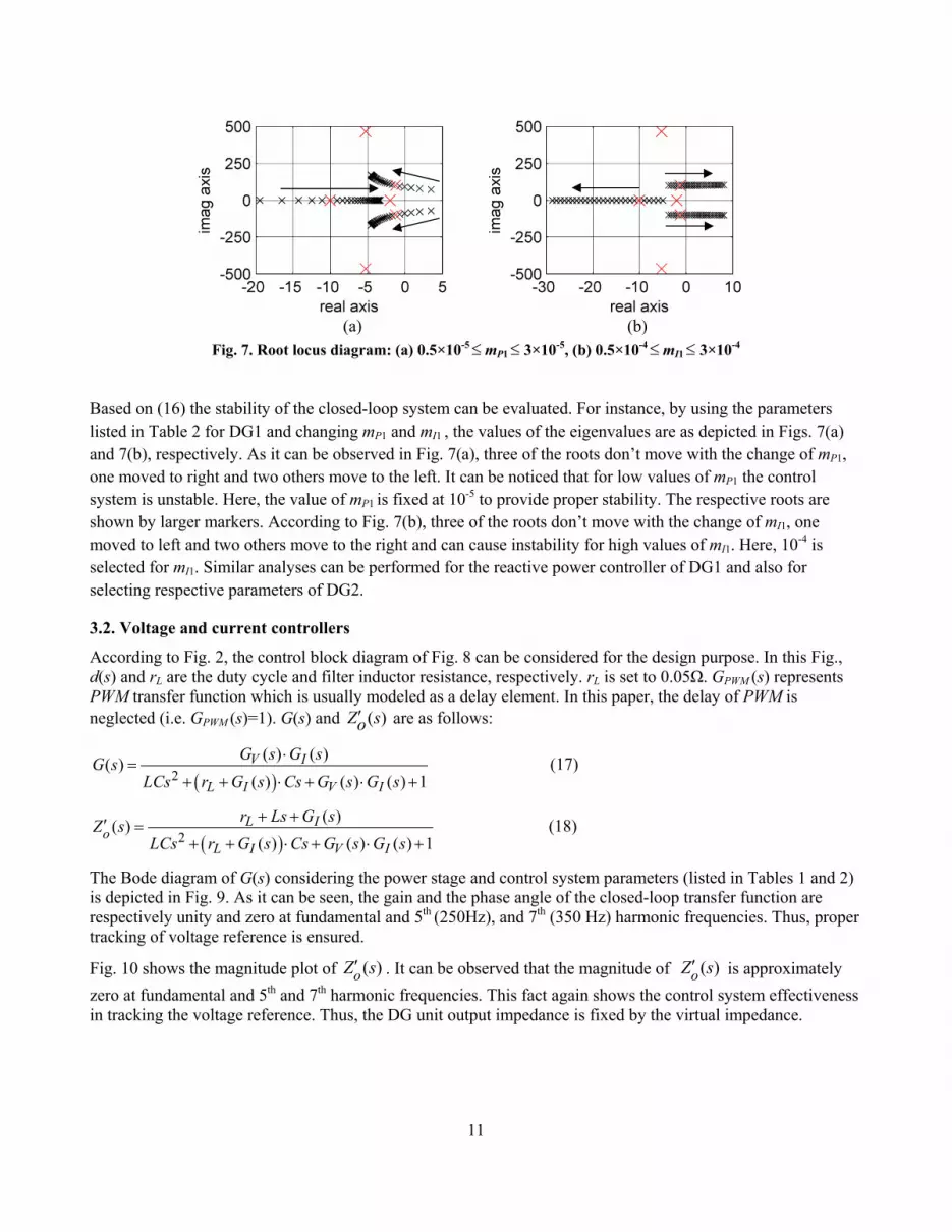
Fig. 7. Root locus diagram: (a) 0.5×10⁻⁵≤mP1≤ 3×10⁻⁵, (b) 0.5×10⁻⁴≤mI1≤ 3×10⁻⁴
Based on (16) the stability of the closed-loop system can be evaluated. For instance, by using the parameters listed in Table 2 for DG1 and changing mP1 and mI1 , the values of the eigenvalues are as depicted in Figs. 7(a) and 7(b), respectively. As it can be observed in Fig. 7(a), three of the roots don’t move with the change of mP1, one moved to right and two others move to the left. It can be noticed that for low values of mP1 the control system is unstable. Here, the value of mP1 is fixed at 10-5 to provide proper stability. The respective roots are shown by larger markers. According to Fig. 7(b), three of the roots don’t move with the change of mI1, one moved to left and two others move to the right and can cause instability for high values of mI1. Here, 10-4 is selected for mI1. Similar analyses can be performed for the reactive power controller of DG1 and also for selecting respective parameters of DG2.
3.2. Voltage and current controllers
According to Fig. 2, the control block diagram of Fig. 8 can be considered for the design purpose. In this Fig., d(s) and rL are the duty cycle and filter inductor resistance, respectively. rL is set to 0.05Ω. GPWM (s) represents PWM transfer function which is usually modeled as a delay element. In this paper, the delay of PWM is neglected (i.e. GPWM (s)=1). G(s) and ( )Z so′ are as follows:
( )2( ) ( )( )
( ) ( ) ( ) 1V I
L I V I
G s G sG sLCs r G s Cs G s G s
⋅=
+ + ⋅ + ⋅ + (17)
( )2( )( )
( ) ( ) ( ) 1L I
oL I V I
r Ls G sZ sLCs r G s Cs G s G s
+ +′ =+ + ⋅ + ⋅ +
(18)
The Bode diagram of G(s) considering the power stage and control system parameters (listed in Tables 1 and 2) is depicted in Fig. 9. As it can be seen, the gain and the phase angle of the closed-loop transfer function are respectively unity and zero at fundamental and 5th (250Hz), and 7th (350 Hz) harmonic frequencies. Thus, proper tracking of voltage reference is ensured.
Fig. 10 shows the magnitude plot of ( )oZ s′ . It can be observed that the magnitude of ( )oZ s′ is approximately zero at fundamental and 5th and 7th harmonic frequencies. This fact again shows the control system effectiveness in tracking the voltage reference. Thus, the DG unit output impedance is fixed by the virtual impedance.

12
Fig. 8. Model of DG power stage and control system.
Fig. 9. Bode diagram of closed loop transfer function.
Fig. 10. Magnitude plot of ( )Z so′
( )d s( )ref sv ( )dcV d s⋅
( )C si( )L si
*( )si − ( )PWMG s( )VG s +
dcV
⊗ − LsLr +1
+
( )o si( )Z sv
+−− −
Cs1 ( )v so
Power Stage
SystemControl
+ ÷×
PWM Inverter
( )IG s
Mag
nitu
de (d
B)
Frequency (Hz)
Ph
ase
(deg
) M
agni
tude
(dB
)
Frequency (Hz)

13
3.3. Virtual impedance
As mentioned before, the fundamental virtual impedance parameters should be selected in a way that the electrical system is kept mainly inductive. Also, small virtual resistance is added to make the system oscillations more damped. In this paper, a two-DG microgrid is considered as the test system. The values listed in Table 2 are selected as the DGs fundamental virtual impedance. According to these values, the phase angles of DGs output impedance are set to about 81°. Furthermore, by adding DGs tie line impedances (listed in Table 1) to the output impedances, the total impedance between each DG and PCC can be calculated. According to this, the phase angles of the total impedances are about 76° and 79° for DG1 and DG2, respectively. Thus, the mainly inductive behavior is provided.
As demonstrated in Fig. 10, the magnitude of ( )Z so′ is very low at harmonic frequencies. Hence, the values of distribution line impedances between DG units and load bus significantly affect the harmonic load sharing among DGs. Thus, the virtual resistance values at harmonic frequencies should be high enough to mitigate the effect of distribution lines effectively and a proper sharing of harmonic current can be provided. It should be noted that some amount of sharing error can be acceptable especially in the cases that the inverters are not operating at their power limit. In addition, note that the sharing improvement is achieved at the expense of distorting DG output voltage as a result of harmonic voltage drop on Rv,h. Thus, for selection of Rv,h a trade-off should be considered between the amount of output voltage distortion and nonlinear load sharing accuracy. It is also noteworthy that the rating of DGs interface converters should be taken into account. Here, the values shown in Table 2 are selected as DGs Rv,h.
3.4. Harmonic compensator
CGh should be selected according to the required amount of compensation. In fact, by increase of CGh, the hth harmonic of PCC voltage is more compensated. In practical application, the value of CGh can be controlled by an up-down counter according the required harmonic distortion at PCC as explained in [21]. However, as it will be shown later, PCC voltage compensation is achieved by the change of DGs output distortion and it is possible that the output voltage distortions of some DGs are increased. In some cases (e.g. connection of sensitive loads at DG terminal) the maximum distortion of DG output voltage should be kept below a pre-determined value and it can restrict the maximum value of CGh. Also, it should be noted that using very high values for CGh can make the control system unstable.
4. Simulation results
The electrical system of Fig. 11 which comprises a two-DG grid-connected microgrid and the utility grid is considered as the test system. DG1 is rated at double power comparing to DG2 (S01=2S02). The microgrid and utility grid are rated at 230V (phase rms voltage) and 50Hz. It is assumed that the grid voltage is distorted by 3% (of fundamental voltage) 5th and 7th voltage harmonics. Switching frequency of the DGs inverters is 10 kHz. A diode rectifier is considered as the nonlinear load; also, a star-connected linear load (ZL) is connected to PCC.
As it can be seen in Table 1, 1Z is considered double of 2Z in order to simulate asymmetrical DG tie lines. In order to simulate a general case, resistive-inductive impedances are considered for the tie lines. The parameters of power controllers and virtual impedances are selected considering the different ratings of the DGs (S01=2S02) while the parameters of voltage and current controllers are the same for both DGs. DG1 and DG2 reference values of fundamental active powers are 1
* 2000P W= and 2* 1000P W= , respectively while the reference
reactive powers are set to 1* 500Q VAr= and *
2 250Q VAr= .

14
Fig. 11. Test system for simulation studies.
Table 1. Power stage parameters
dc link voltage
LC filter inductance
LC filter capacitance nonlinear load tie line
( )dcV V ( )L mH ( )C Fμ ( )Z Ω 650 1.8 25 0.15+j0.4712
DG1/DG2 tie line nonlinear load utility tie line linear load
1( )Z Ω / 2 ( )Z Ω ( )NLC Fμ / ( )NLR Ω / ( )NLL mH ( )g tZ Z+ Ω ( )LZ Ω
0.3+j0.9424/0.15+j0.4712 235/100/0.084 1+j1.8848 50+j6.28
Table 2. Control system parameters
power controllers mP1
(rad/W) mI1
(rad/W.s) nP1
(V/VAr) nI1
(V/VAr.s) mP2
(rad/W) mI2
(rad/W.s) nP2
(V/VAr) nI2
(V/VAr.s) 10-5 10-4 0.05 0.1 2×10⁻⁵ 2×10⁻⁴ 0.1 0.2
virtual impedance Rv1
(Ω)
Lv1
(mH)
Rv2
(Ω)Lv2
(mH)Rv,h1 (Ω)
Rv,h2
(Ω)0.1 2 0.2 4 4 8
voltage controller
pVk 1rVk 5rVk 7rVk 1cVω (rad/s)
5cVω (rad/s)
7cVω
(rad/s) 1 100 100 175 1 1 1
current controller
pIk 1rIk 5rIk 7rIk 1cIω (rad/s)
5cIω (rad/s)
7cIω
(rad/s) 5 1000 100 100 1 1 1
selective harmonic compensator CG5 CG7 -70 -25
PCC
DG2
LinearLoad
2Z
DG12Z
2Z
1Z
1Z
1Z
NonlinearLoad
Z Z Z
NLC
−+
NLRNLL
LZ
Utility Grid
tZ
tZ
tZ
gZ
gZ
gZ
Microgrid

15
Table 3. Voltage waveforms at different simulation steps DG1 DG2 PCC
step1
step2
step3
Simulations are performed in MATLAB/Simulink using SimPowerSystems toolbox. Three simulation steps are considered:
Step1 ( 0 2t s≤ < ): DGs operate with only fundamental virtual impedance and harmonic compensation is not acting. Step2 ( 2 3.5t s≤ < ): Harmonic virtual resistances are added. Step3 ( 3.5 5t s≤ < ): Harmonic compensation is activated.
4.1. Simulation step 1 As seen in Table 3, before activating the harmonic virtual resistance, DGs output voltages are approximately free of harmonic distortion. This fact can be seen in Fig. 12(a)-(c) as very low of total and 5th and 7th harmonic distortions (THD, HD5 and HD7, respectively) of output voltages. It demonstrates the effectiveness of DGs controller in tracking the voltage reference. But, as shown in Table 3 and Fig. 12(a)-(c), PCC voltage is distorted noticeably due to harmonic voltage drop on the DG tie lines. The details of THD calculation can be found in [21]. HD5 and HD7 can be calculated similar to ,I hHD
calculation in Fig. 6.
As shown in Figs. 13(a) and (b), the reference of active and reactive powers are tracked, properly. But, it can be noticed from Fig. 13(c) that before addition of harmonic virtual resistance at t =2s, non-fundamental (harmonic) power (Sn) is shared in inverse proportion to the tie lines impedances and DG2 supplied Sn is approximately double while it has half rated power.
Sn is calculated according to the following equation [19]:
( ) ( )22n I VfS S THD THD= ⋅ + (19)

16
where Sf , THDI and THDV are the fundamental apparent power ( 2 2f PS Q= + ) and total harmonic
distortions of current and voltage, respectively. DGs output current harmonic spectrums in Step 1 are depicted in Fig. 14(a). These spectrums are achieved by applying DG1 fundamental current as the common base for both DGs. It can be observed that fundamental components (first harmonic) of DGs current are shared in proportion to the DGs rating. This result is in compliance with those of Figs. 13(a) and (b). But, other current harmonics are not properly shared. Especially, it can be seen that DG2 5th and 7th current harmonics (main harmonic orders) are approximately double of the 5th and 7th harmonics of DG1. This fact has also been observed in Fig. 13(c) in terms of non-fundamental powers.
(a)
(b)
(c)
Fig. 12. Voltage harmonic distortions (fundamental component=100%) (a) total harmonic distortion, (b) 5th harmonic distortion, (c) 7th harmonic distortion
21 3
17
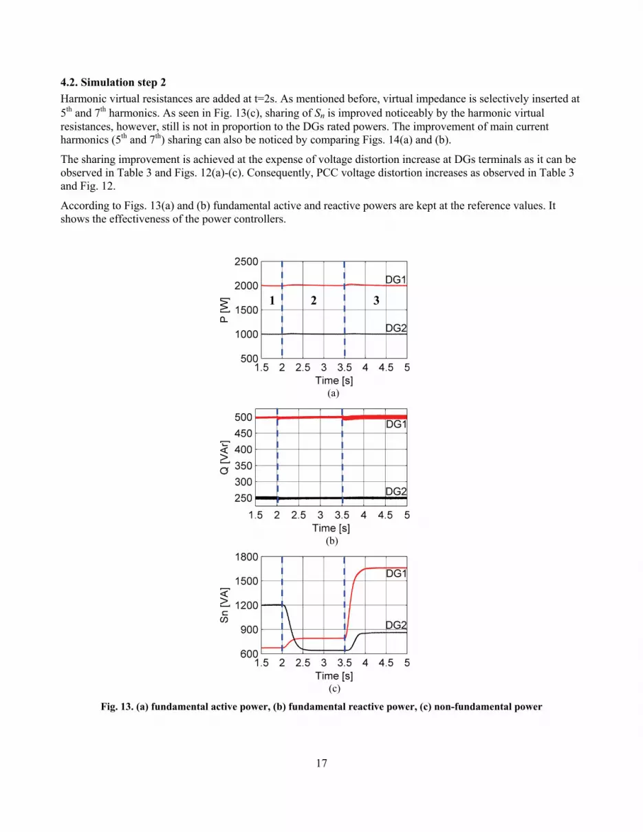
4.2. Simulation step 2 Harmonic virtual resistances are added at t=2s. As mentioned before, virtual impedance is selectively inserted at 5th and 7th harmonics. As seen in Fig. 13(c), sharing of Sn is improved noticeably by the harmonic virtual resistances, however, still is not in proportion to the DGs rated powers. The improvement of main current harmonics (5th and 7th) sharing can also be noticed by comparing Figs. 14(a) and (b).
The sharing improvement is achieved at the expense of voltage distortion increase at DGs terminals as it can be observed in Table 3 and Figs. 12(a)-(c). Consequently, PCC voltage distortion increases as observed in Table 3 and Fig. 12.
According to Figs. 13(a) and (b) fundamental active and reactive powers are kept at the reference values. It shows the effectiveness of the power controllers.
(a)
(b)
(c)
Fig. 13. (a) fundamental active power, (b) fundamental reactive power, (c) non-fundamental power
21 3

18
4.3. Simulation step 3 In the next simulation step, selective compensation of PCC voltage main harmonics is activated at t =3.5s. As seen in Figs. 12(b) and (c), HD5 and HD7 of PCC voltage are mitigated, effectively. It leads to significant reduction of PCC voltage THD according to Fig. 12(a). Improvement of PCC voltage quality can also be observed in Table 3.
Also, it can be observed in Table 3 and Figs. 12(a)-(c) that the harmonic compensation is achieved by the increase of DG1 output voltage distortion. Note that DG1 tie line impedance is relatively high; also, the nonlinear load supplied by this DG is higher than the amount supplied by DG2. Thus, before compensation, the harmonic voltage drops over DG1 tie line and its harmonic virtual resistance distort PCC voltage, noticeably. Hence, after compensation activation, the output voltage of this DG has become distorted in order to compensate these harmonic voltage drops and provide approximately sinusoidal voltage at PCC. On the other hand, due to low value of the tie line impedance and non-fundamental power of DG2, harmonic distortion of PCC and DG2 change with approximately similar behavior, as seen in Fig. 12 and Table 3.
(a)
(b)
(c)
Fig. 14. DGs current spectrum (fundamental component of DG1, I1,rms=100%) (a) step 1 (I1,rms=3.02A), (b) step 2 (I1,rms=3.04A), (c) step 3 (I1,rms=3.03A)

19
Moreover, as depicted in Fig 13(c), DGs non-fundamental powers increase as a result of harmonic compensation. It is mainly originated from the increase of main harmonic currents supplied by the DGs as shown in Fig. 14(c). As seen, DGs 5th and 7th current harmonics are increased significantly at simulation step 3 to provide compensation of respective voltage harmonics. Thus, as mentioned in subsection 2.5, compensation effort can be considered as the amount of current harmonic distortion ( ,I hHD
in Fig. 6) increase. Due to double
rated power of DG1, the compensation should be more supported by this DG. This fact can be observed in Figs. 13(c) and 14(c) as noticeably more increase of DG1 non-fundamental power and current distortion, respectively. It demonstrates the effectiveness of the proposed approach for sharing of compensation effort.
Furthermore, as shown in Fig. 13(c) sharing of non-fundamental powers is improved, significantly, after harmonic compensation and Sn is shared approximately in proportion of the DGs rating. The proper sharing is provided by harmonic virtual resistances as well as compensation effort sharing. In addition, fundamental powers references are tracked in this simulation step according to Figs. 13(a) and (b).
5. Conclusions
A new method has been proposed for selective compensation of PCC voltage main harmonics in a grid-connected microgrid. Harmonic compensation is achieved through proper control of DGs interface converters. The compensation effort of each harmonic is shared based on a novel approach which considers the respective harmonic distortion. Furthermore, a selective virtual resistance loop is included in the control system of each DG in order to improve non-fundamental power sharing. The control system design is discussed and simulation results are provided. The presented simulation results show that by application of the proposed method, PCC voltage quality is improved significantly. Also, DGs supplied fundamental and non-fundamental powers are in proportion to their rated powers.
References
[1] H. Akagi, Y. Kanagawa, A. Nabase, Instantaneous reactive power compensator comprising switching devices without energy storage components, IEEE Trans. Ind. Appl. IA-20 (3) (1984) 625-630.
[2] H. Akagi, Control strategy and site selection of a shunt active filter for damping of harmonic propagation in power distribution systems, IEEE Trans. Power Deliv. 12 (1) (1997) 354-363.
[3] E. Barklund, N. Pogaku, M. Prodanovic, C.H. Aramburo, T.C. Green, Energy management in autonomous microgrid using stability-constrained droop control of inverters, IEEE Trans. Power Electron. 23 (5) (2008) 2346-2352.
[4] F. Blaabjerg, Z. Chen, S.B. Kjaer, Power electronics as efficient interface in dispersed power generation systems, IEEE Trans. Power Electron. 19 (5) (2004) 1184-1194.
[5] F. Blaabjerg, R. Teodorescu, M. Liserre, A.V. Timbus, Overview of control and grid synchronization for distributed power generation systems, IEEE Trans. Ind. Electron. 53 (5) (2006) 1398-1409.
[6] U. Borup, F. Blaabjerg, P.N. Enjeti, Sharing of nonlinear load in parallel-connected three-phase converters, IEEE Trans. Ind. Appl. 37 (6) (2001) 1817–1823.
[7] S.J. Chiang, C.Y. Yen, K.T. Chang, A multimodule parallelable series-connected PWM voltage regulator, IEEE Trans. Ind. Electron. 48 (3) (2001) 506-516.
[8] S.J. Chiang, J.M. Chang, “Parallel control of the UPS inverters with frequency-dependent droop scheme, Power Electron. Specialist Conf. PESC (2001), 957–961.
[9] M. Cirrincione, M. Pucci, G. Vitale, A single-phase DG generation unit with shunt active power filter capability by adaptive neural filtering, IEEE Trans. Ind. Electron. 55 (5) (2008) 2093-2110.

20
[10] R.C. Dugan, M.F. McGranaghan, S. Santoso, H.W. Beaty, Electrical Power Systems Quality, second ed., McGraw-Hill, New York, 2003.
[11] D. De, V. Ramanarayanan, Decentralized parallel operation of inverters sharing unbalanced and nonlinear loads, IEEE Trans. Power Electron. 25 (12) (2010) 3015-3025.
[12] J.M. Guerrero, L.G. Vicuna, J. Matas, M. Castilla, J. Miret, Output impedance design of parallel connected UPS inverters with wireless load sharing control, IEEE Trans. Ind. Electron. 52 (4) (2005) 1126-1135.
[13] J.M. Guerrero, J. Matas, L.G. de Vicuña, M. Castilla, J. Miret, Wireless-control strategy for parallel operation of distributed-generation inverters, IEEE Trans. Ind. Electron. 53 (5) (2006) 1461-1470.
[14] J.M. Guerrero, J. Matas, L.G. de Vicuña, M. Castilla, J. Miret, Decentralized control for parallel operation of distributed generation inverters using resistive output impedance, IEEE Trans. Ind. Electron. 54 (2) (2007) 994-1004.
[15] J.M. Guerrero, J.C. Vasquez, J. Matas, L.G. de Vicuña, M. Castilla, Hierarchical control of droop-controlled AC and DC microgrids—a general approach toward standardization, IEEE Trans. Ind. Electron. 58 (1) (2011) 158-172.
[16] J. He, Y.W. Li, Analysis and design of interfacing inverter output virtual impedance in a low voltage microgrid, Energy Conv. Cong. and Exp. ECCE (2010), 2857–2864.
[17] J. He, Y.W. Li, M.S. Munir, A flexible harmonic control approach through voltage controlled DG-grid interfacing converters, IEEE Trans. Ind. Electron., Early Access (2011).
[18] IEEE Standard 519-1992, IEEE recommended practices and requirements for harmonic control in electrical power systems (1992).
[19] IEEE Standard 1459-2010, IEEE standard definitions for the measurement of electric power quantities under sinusoidal, nonsinusoidal, balanced, or unbalanced conditions (2010).
[20] IEEE Standard 1547.4-2011, IEEE guide for design, operation, and integration of distributed resource island systems with electric power systems (2011).
[21] P. Jintakosonwit, H. Akagi, H. Fujita, S. Ogasawara, Implementation and performance of automatic gain adjustment in a shunt active filter for harmonic damping throughout a power distribution system, IEEE Trans. Power Electron. 17 (3) (2002) 438-447.
[22] M. Karimi-Ghartemani, O. Boon-Teck, A. Bakhshai, Application of enhanced phase-locked loop system to the computation of synchrophasors, IEEE Trans. Power Deliv. 26 (1) (2011) 22-32.
[23] C. Lascu, L. Asiminoaei, I. Boldea, F. Blaabjerg, High performance current controller for selective harmonic compensation in active power filters, IEEE Trans. Power Electron. 22 (5) (2007) 1826-1835.
[24] T.L. Lee, P.T. Cheng, Design of a new cooperative harmonic filtering strategy for distributed generation interface converters in an islanding network, IEEE Trans. Power Electron. 22 (5) (2007) 1919-1927.
[25] T.L. Lee, J.C. Li, P.T. Cheng, Discrete frequency tuning active filter for power system harmonics, IEEE Trans. Power Electron. 24 (5) (2009) 1209-1217.
[26] Y. Li, D.M. Vilathgamuwa, P.C. Loh, Design, analysis, and real-time testing of a controller for multibus microgrid system, IEEE Trans. Power Electron. 19 (5) (2004) 1195-1204.
[27] M.I. Marei, E.F. El-Saadany, M.M.A. Salama, A novel control algorithm for the DG interface to mitigate power quality problem, IEEE Trans. Power Deliv. 19 (3) (2004) 1384-1392.
[28] P. Mattavelli, F.P. Marafão, Repetitive-based control for selective harmonic compensation in active power filters, IEEE Trans. Ind. Electron. 51 (5) (2004) 1018-1024.
[29] F.Z. Peng, G.W. Ott, D.J. Adams, Harmonic and reactive power compensation based on the generalized instantaneous reactive power theory for three-phase four-wire systems, IEEE Trans. Power Electron. 13 (6) (1998) 1174-1181.
[30] N. Pogaku, T.C. Green, Harmonic mitigation throughout a distribution system: a distributed-generator-based solution, IEE Proc.-Gener. Transm. Distrib. 153 (3) (2006) 350-358.
[31] M. Prodanovic, K.D. Brabandere, J.V. Keybus, T.C. Green, J. Driesen, Harmonic and reactive power compensation as ancillary services in inverter-based distributed generation, IET Gener. Transm. Distrib. 1 (3) (2007) 432-438.
[32] P. Rodriguez, A. Luna, I. Candela, R. Mujal, R. Teodorescu, F. Blaabjerg, Multiresonant frequency-locked loop for grid synchronization of power converters under distorted grid conditions, IEEE Trans. Ind. Electron. 58 (1) (2011) 127-138.

21
[33] M. Savaghebi, A. Jalilian, J.C. Vasquez, J.M. Guerrero, T.L. Lee, Voltage harmonic compensation of a microgrid operating in islanded and grid-connected modes, 19th Iranian Conf. of Elec. Eng. ICEE (2011), 1-6.
[34] T. Takeshita, N. Matsui, Current waveform control of PWM converter system for harmonic suppression on distribution system, IEEE Trans. Ind. Electron. 50 (6) (2003) 1134-1139.
[35] A.G. Tsikalakis, N.D. Hatziargyriou, Centralized control for optimizing microgrids operation, IEEE Trans. Energy Conv. 23 (1) (2008) 241-248.
[36] J.C. Vasquez, R.A. Mastromauro, J.M. Guerrero, M. Liserre, Voltage support provided by a droop-controlled multifunctional inverter, IEEE Trans. Ind. Electron. 56 (11) (2009) 4510-4519.
[37] J.C. Vasquez, J.M. Guerrero, M. Savaghebi, R. Teodorescu, Modeling, analysis, and design of stationary reference frame droop controlled parallel three-phase voltage source inverters, 8th Int. Conf. on Power Electron. ICPE (2011) 272-279.
[38] K. Wada, H. Fujita, H. Akagi, “Considerations of a shunt active filter based on voltage detection for installation on a long distribution feeder,” IEEE Trans. Ind. Appl. 38 (4) (2002) 1123-1130.


