Embed Size (px)
Citation preview

Semiconductor Components Industries, LLC, 1999
December, 1999 – Rev. 61 Publication Order Number:
SN74LS00/D
• ESD > 3500 Volts
14 13 12 11 10 9
1 2 3 4 5 6
VCC
8
7
GND
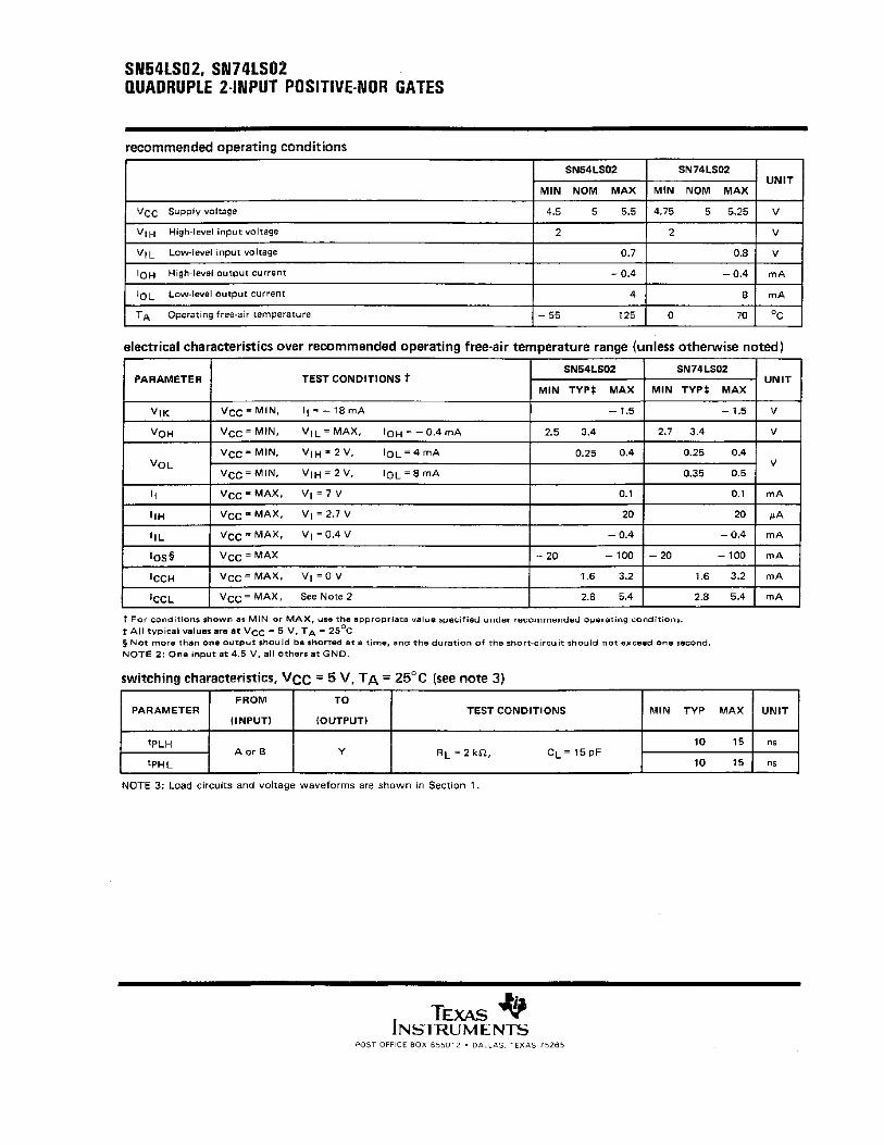
GUARANTEED OPERATING RANGES
Symbol Parameter Min Typ Max Unit
VCC Supply Voltage 4.75 5.0 5.25 V
TA Operating AmbientTemperature Range
0 25 70 °C
IOH Output Current – High –0.4 mA
IOL Output Current – Low 8.0 mA
LOWPOWER
SCHOTTKY
Device Package Shipping
ORDERING INFORMATION
SN74LS00N 14 Pin DIP 2000 Units/Box
SN74LS00D 14 Pin
SOICD SUFFIX
CASE 751A
http://onsemi.com
2500/Tape & Reel
PLASTICN SUFFIXCASE 646
14
1
14
1

SN74LS00
http://onsemi.com2
DC CHARACTERISTICS OVER OPERATING TEMPERATURE RANGE (unless otherwise specified)
Limits
Symbol Parameter Min Typ Max Unit Test Conditions
VIH Input HIGH Voltage 2.0 VGuaranteed Input HIGH Voltage for
All Inputs
VIL Input LOW Voltage0.8
VGuaranteed Input LOW Voltage for
All Inputs
VIK Input Clamp Diode Voltage –0.65 –1.5 V VCC = MIN, IIN = –18 mA
VOH Output HIGH Voltage2.7 3.5 V VCC = MIN, IOH = MAX, VIN = VIH
or VIL per Truth Table
VOL Output LOW Voltage0.25 0.4 V IOL = 4.0 mA VCC = VCC MIN,
VIN = VIL or VIHVOL Out ut LOW Voltage0.35 0.5 V IOL = 8.0 mA
VIN = VIL or VIHper Truth Table
IIH Input HIGH Current20 µA VCC = MAX, VIN = 2.7 V
IIH In ut HIGH Current0.1 mA VCC = MAX, VIN = 7.0 V
IIL Input LOW Current –0.4 mA VCC = MAX, VIN = 0.4 V
IOS Short Circuit Current (Note 1) –20 –100 mA VCC = MAX
Power Supply Current
ICC Total, Output HIGH 1.6 mA VCC = MAX
Total, Output LOW 4.4
Note 1: Not more than one output should be shorted at a time, nor for more than 1 second.
AC CHARACTERISTICS (TA = 25°C)
Limits
Symbol Parameter Min Typ Max Unit Test Conditions
tPLH Turn–Off Delay, Input to Output 9.0 15 ns VCC = 5.0 V
tPHL Turn–On Delay, Input to Output 10 15 nsCC
CL = 15 pF

SN74LS00
http://onsemi.com3
PACKAGE DIMENSIONS
1 7
14 8
B
A DIM MIN MAX MIN MAXMILLIMETERSINCHES
A 0.715 0.770 18.16 18.80B 0.240 0.260 6.10 6.60C 0.145 0.185 3.69 4.69D 0.015 0.021 0.38 0.53F 0.040 0.070 1.02 1.78G 0.100 BSC 2.54 BSCH 0.052 0.095 1.32 2.41J 0.008 0.015 0.20 0.38K 0.115 0.135 2.92 3.43LM ––– 10 ––– 10 N 0.015 0.039 0.38 1.01
NOTES:1. DIMENSIONING AND TOLERANCING PER ANSI
Y14.5M, 1982.2. CONTROLLING DIMENSION: INCH.3. DIMENSION L TO CENTER OF LEADS WHEN
FORMED PARALLEL.4. DIMENSION B DOES NOT INCLUDE MOLD FLASH.5. ROUNDED CORNERS OPTIONAL.
F
H G DK
C
SEATINGPLANE
N
–T–
14 PL
M0.13 (0.005)
L
MJ
0.290 0.310 7.37 7.87
NOTES:1. DIMENSIONING AND TOLERANCING PER ANSI
Y14.5M, 1982.2. CONTROLLING DIMENSION: MILLIMETER.3. DIMENSIONS A AND B DO NOT INCLUDE
MOLD PROTRUSION.4. MAXIMUM MOLD PROTRUSION 0.15 (0.006)
PER SIDE.5. DIMENSION D DOES NOT INCLUDE DAMBAR
PROTRUSION. ALLOWABLE DAMBARPROTRUSION SHALL BE 0.127 (0.005) TOTALIN EXCESS OF THE D DIMENSION ATMAXIMUM MATERIAL CONDITION.
–A–
–B–
G
P 7 PL
14 8
71M0.25 (0.010) B M
SBM0.25 (0.010) A ST
–T–
FR X 45
SEATINGPLANE
D 14 PL K
C
JM
DIM MIN MAX MIN MAX
INCHESMILLIMETERS
A 8.55 8.75 0.337 0.344B 3.80 4.00 0.150 0.157C 1.35 1.75 0.054 0.068D 0.35 0.49 0.014 0.019F 0.40 1.25 0.016 0.049G 1.27 BSC 0.050 BSCJ 0.19 0.25 0.008 0.009K 0.10 0.25 0.004 0.009M 0 7 0 7 P 5.80 6.20 0.228 0.244R 0.25 0.50 0.010 0.019
D SUFFIXPLASTIC SOIC PACKAGE
CASE 751A–03ISSUE F
N SUFFIXPLASTIC PACKAGE
CASE 646–06ISSUE M

SN74LS00
http://onsemi.com4
ON Semiconductor and are trademarks of Semiconductor Components Industries, LLC (SCILLC). SCILLC reserves the right to make changeswithout further notice to any products herein. SCILLC makes no warranty, representation or guarantee regarding the suitability of its products for any particularpurpose, nor does SCILLC assume any liability arising out of the application or use of any product or circuit, and specifically disclaims any and all liability,including without limitation special, consequential or incidental damages. “Typical” parameters which may be provided in SCILLC data sheets and/orspecifications can and do vary in different applications and actual performance may vary over time. All operating parameters, including “Typicals” must bevalidated for each customer application by customer’s technical experts. SCILLC does not convey any license under its patent rights nor the rights of others.SCILLC products are not designed, intended, or authorized for use as components in systems intended for surgical implant into the body, or other applicationsintended to support or sustain life, or for any other application in which the failure of the SCILLC product could create a situation where personal injury ordeath may occur. Should Buyer purchase or use SCILLC products for any such unintended or unauthorized application, Buyer shall indemnify and holdSCILLC and its officers, employees, subsidiaries, affiliates, and distributors harmless against all claims, costs, damages, and expenses, and reasonableattorney fees arising out of, directly or indirectly, any claim of personal injury or death associated with such unintended or unauthorized use, even if such claimalleges that SCILLC was negligent regarding the design or manufacture of the part. SCILLC is an Equal Opportunity/Affirmative Action Employer.
PUBLICATION ORDERING INFORMATIONASIA/PACIFIC : LDC for ON Semiconductor – Asia SupportPhone : 303–675–2121 (Tue–Fri 9:00am to 1:00pm, Hong Kong Time)
Toll Free from Hong Kong 800–4422–3781Email : ONlit–[email protected]
JAPAN : ON Semiconductor, Japan Customer Focus Center4–32–1 Nishi–Gotanda, Shinagawa–ku, Tokyo, Japan 141–8549Phone : 81–3–5487–8345Email : [email protected]
Fax Response Line : 303–675–2167800–344–3810 Toll Free USA/Canada
ON Semiconductor Website: http://onsemi.com
For additional information, please contact your localSales Representative.
SN74LS00/D
North America Literature Fulfillment :Literature Distribution Center for ON SemiconductorP.O. Box 5163, Denver, Colorado 80217 USAPhone : 303–675–2175 or 800–344–3860 Toll Free USA/CanadaFax: 303–675–2176 or 800–344–3867 Toll Free USA/CanadaEmail : [email protected]
N. American Technical Support : 800–282–9855 Toll Free USA/Canada
EUROPE: LDC for ON Semiconductor – European SupportGerman Phone: (+1) 303–308–7140 (M–F 2:30pm to 5:00pm Munich Time)
Email: ONlit–[email protected] Phone: (+1) 303–308–7141 (M–F 2:30pm to 5:00pm Toulouse Time)
Email: ONlit–[email protected] Phone: (+1) 303–308–7142 (M–F 1:30pm to 5:00pm UK Time)
Email: [email protected]


PACKAGING INFORMATION
Orderable Device Status (1) PackageType
PackageDrawing
Pins PackageQty
Eco Plan (2) Lead/Ball Finish MSL Peak Temp (3)
JM38510/00401BCA ACTIVE CDIP J 14 1 TBD Call TI Level-NC-NC-NC
JM38510/00401BDA ACTIVE CFP W 14 1 TBD Call TI Level-NC-NC-NC
JM38510/00401BDA ACTIVE CFP W 14 1 TBD Call TI Level-NC-NC-NC
JM38510/07301BCA ACTIVE CDIP J 14 1 TBD Call TI Level-NC-NC-NC
JM38510/07301BCA ACTIVE CDIP J 14 1 TBD Call TI Level-NC-NC-NC
JM38510/07301BDA ACTIVE CFP W 14 1 TBD Call TI Level-NC-NC-NC
JM38510/07301BDA ACTIVE CFP W 14 1 TBD Call TI Level-NC-NC-NC
JM38510/30301B2A ACTIVE LCCC FK 20 1 TBD Call TI Level-NC-NC-NC
JM38510/30301B2A ACTIVE LCCC FK 20 1 TBD Call TI Level-NC-NC-NC
JM38510/30301BCA ACTIVE CDIP J 14 1 TBD Call TI Level-NC-NC-NC
JM38510/30301BCA ACTIVE CDIP J 14 1 TBD Call TI Level-NC-NC-NC
JM38510/30301BDA ACTIVE CFP W 14 1 TBD Call TI Level-NC-NC-NC
JM38510/30301BDA ACTIVE CFP W 14 1 TBD Call TI Level-NC-NC-NC
JM38510/30301SCA ACTIVE CDIP J 14 1 TBD Call TI Level-NC-NC-NC
JM38510/30301SCA ACTIVE CDIP J 14 1 TBD Call TI Level-NC-NC-NC
JM38510/30301SDA ACTIVE CFP W 14 1 TBD Call TI Level-NC-NC-NC
JM38510/30301SDA ACTIVE CFP W 14 1 TBD Call TI Level-NC-NC-NC
SN5402J ACTIVE CDIP J 14 1 TBD Call TI Level-NC-NC-NC
SN5402J ACTIVE CDIP J 14 1 TBD Call TI Level-NC-NC-NC
SN54LS02J ACTIVE CDIP J 14 1 TBD Call TI Level-NC-NC-NC
SN54LS02J ACTIVE CDIP J 14 1 TBD Call TI Level-NC-NC-NC
SN54S02J ACTIVE CDIP J 14 1 TBD Call TI Level-NC-NC-NC
SN54S02J ACTIVE CDIP J 14 1 TBD Call TI Level-NC-NC-NC
SN7402N ACTIVE PDIP N 14 25 Pb-Free(RoHS)
CU NIPDAU Level-NC-NC-NC
SN7402N ACTIVE PDIP N 14 25 Pb-Free(RoHS)
CU NIPDAU Level-NC-NC-NC
SN7402N3 OBSOLETE PDIP N 14 TBD Call TI Call TI
SN7402N3 OBSOLETE PDIP N 14 TBD Call TI Call TI
SN7402NE4 ACTIVE PDIP N 14 25 Pb-Free(RoHS)
CU NIPDAU Level-NC-NC-NC
SN7402NE4 ACTIVE PDIP N 14 25 Pb-Free(RoHS)
CU NIPDAU Level-NC-NC-NC
SN74LS02D ACTIVE SOIC D 14 50 Green (RoHS &no Sb/Br)
CU NIPDAU Level-1-260C-UNLIM
SN74LS02D ACTIVE SOIC D 14 50 Green (RoHS &no Sb/Br)
CU NIPDAU Level-1-260C-UNLIM
SN74LS02DE4 ACTIVE SOIC D 14 50 Green (RoHS &no Sb/Br)
CU NIPDAU Level-1-260C-UNLIM
SN74LS02DE4 ACTIVE SOIC D 14 50 Green (RoHS &no Sb/Br)
CU NIPDAU Level-1-260C-UNLIM
SN74LS02DR ACTIVE SOIC D 14 2500 Green (RoHS &no Sb/Br)
CU NIPDAU Level-1-260C-UNLIM
SN74LS02DR ACTIVE SOIC D 14 2500 Green (RoHS &no Sb/Br)
CU NIPDAU Level-1-260C-UNLIM
PACKAGE OPTION ADDENDUM
www.ti.com 17-Oct-2005
Addendum-Page 1

Orderable Device Status (1) PackageType
PackageDrawing
Pins PackageQty
Eco Plan (2) Lead/Ball Finish MSL Peak Temp (3)
SN74LS02DRE4 ACTIVE SOIC D 14 2500 Green (RoHS &no Sb/Br)
CU NIPDAU Level-1-260C-UNLIM
SN74LS02DRE4 ACTIVE SOIC D 14 2500 Green (RoHS &no Sb/Br)
CU NIPDAU Level-1-260C-UNLIM
SN74LS02J OBSOLETE CDIP J 14 TBD Call TI Call TI
SN74LS02J OBSOLETE CDIP J 14 TBD Call TI Call TI
SN74LS02N ACTIVE PDIP N 14 25 Pb-Free(RoHS)
CU NIPDAU Level-NC-NC-NC
SN74LS02N ACTIVE PDIP N 14 25 Pb-Free(RoHS)
CU NIPDAU Level-NC-NC-NC
SN74LS02N3 OBSOLETE PDIP N 14 TBD Call TI Call TI
SN74LS02N3 OBSOLETE PDIP N 14 TBD Call TI Call TI
SN74LS02NE4 ACTIVE PDIP N 14 25 Pb-Free(RoHS)
CU NIPDAU Level-NC-NC-NC
SN74LS02NE4 ACTIVE PDIP N 14 25 Pb-Free(RoHS)
CU NIPDAU Level-NC-NC-NC
SN74LS02NSR ACTIVE SO NS 14 2000 Green (RoHS &no Sb/Br)
CU NIPDAU Level-1-260C-UNLIM
SN74LS02NSR ACTIVE SO NS 14 2000 Green (RoHS &no Sb/Br)
CU NIPDAU Level-1-260C-UNLIM
SN74LS02NSRG4 ACTIVE SO NS 14 2000 Green (RoHS &no Sb/Br)
CU NIPDAU Level-1-260C-UNLIM
SN74LS02NSRG4 ACTIVE SO NS 14 2000 Green (RoHS &no Sb/Br)
CU NIPDAU Level-1-260C-UNLIM
SN74S02D ACTIVE SOIC D 14 50 Green (RoHS &no Sb/Br)
CU NIPDAU Level-1-260C-UNLIM
SN74S02D ACTIVE SOIC D 14 50 Green (RoHS &no Sb/Br)
CU NIPDAU Level-1-260C-UNLIM
SN74S02DE4 ACTIVE SOIC D 14 50 Green (RoHS &no Sb/Br)
CU NIPDAU Level-1-260C-UNLIM
SN74S02DE4 ACTIVE SOIC D 14 50 Green (RoHS &no Sb/Br)
CU NIPDAU Level-1-260C-UNLIM
SN74S02DR OBSOLETE SOIC D 14 TBD Call TI Call TI
SN74S02DR OBSOLETE SOIC D 14 TBD Call TI Call TI
SN74S02N ACTIVE PDIP N 14 25 Pb-Free(RoHS)
CU NIPDAU Level-NC-NC-NC
SN74S02N ACTIVE PDIP N 14 25 Pb-Free(RoHS)
CU NIPDAU Level-NC-NC-NC
SN74S02N3 OBSOLETE PDIP N 14 TBD Call TI Call TI
SN74S02N3 OBSOLETE PDIP N 14 TBD Call TI Call TI
SN74S02NE4 ACTIVE PDIP N 14 25 Pb-Free(RoHS)
CU NIPDAU Level-NC-NC-NC
SN74S02NE4 ACTIVE PDIP N 14 25 Pb-Free(RoHS)
CU NIPDAU Level-NC-NC-NC
SNJ5402J ACTIVE CDIP J 14 1 TBD Call TI Level-NC-NC-NC
SNJ5402J ACTIVE CDIP J 14 1 TBD Call TI Level-NC-NC-NC
SNJ5402W ACTIVE CFP W 14 1 TBD Call TI Level-NC-NC-NC
SNJ5402W ACTIVE CFP W 14 1 TBD Call TI Level-NC-NC-NC
SNJ54LS02FK ACTIVE LCCC FK 20 1 TBD Call TI Level-NC-NC-NC
PACKAGE OPTION ADDENDUM
www.ti.com 17-Oct-2005
Addendum-Page 2

Orderable Device Status (1) PackageType
PackageDrawing
Pins PackageQty
Eco Plan (2) Lead/Ball Finish MSL Peak Temp (3)
SNJ54LS02FK ACTIVE LCCC FK 20 1 TBD Call TI Level-NC-NC-NC
SNJ54LS02J ACTIVE CDIP J 14 1 TBD Call TI Level-NC-NC-NC
SNJ54LS02J ACTIVE CDIP J 14 1 TBD Call TI Level-NC-NC-NC
SNJ54LS02W ACTIVE CFP W 14 1 TBD Call TI Level-NC-NC-NC
SNJ54LS02W ACTIVE CFP W 14 1 TBD Call TI Level-NC-NC-NC
SNJ54S02FK ACTIVE LCCC FK 20 1 TBD Call TI Level-NC-NC-NC
SNJ54S02FK ACTIVE LCCC FK 20 1 TBD Call TI Level-NC-NC-NC
SNJ54S02J ACTIVE CDIP J 14 1 TBD Call TI Level-NC-NC-NC
SNJ54S02J ACTIVE CDIP J 14 1 TBD Call TI Level-NC-NC-NC
SNJ54S02W ACTIVE CFP W 14 1 TBD Call TI Level-NC-NC-NC
SNJ54S02W ACTIVE CFP W 14 1 TBD Call TI Level-NC-NC-NC
(1) The marketing status values are defined as follows:ACTIVE: Product device recommended for new designs.LIFEBUY: TI has announced that the device will be discontinued, and a lifetime-buy period is in effect.NRND: Not recommended for new designs. Device is in production to support existing customers, but TI does not recommend using this part ina new design.PREVIEW: Device has been announced but is not in production. Samples may or may not be available.OBSOLETE: TI has discontinued the production of the device.
(2) Eco Plan - The planned eco-friendly classification: Pb-Free (RoHS) or Green (RoHS & no Sb/Br) - please checkhttp://www.ti.com/productcontent for the latest availability information and additional product content details.TBD: The Pb-Free/Green conversion plan has not been defined.Pb-Free (RoHS): TI's terms "Lead-Free" or "Pb-Free" mean semiconductor products that are compatible with the current RoHS requirementsfor all 6 substances, including the requirement that lead not exceed 0.1% by weight in homogeneous materials. Where designed to be solderedat high temperatures, TI Pb-Free products are suitable for use in specified lead-free processes.Green (RoHS & no Sb/Br): TI defines "Green" to mean Pb-Free (RoHS compatible), and free of Bromine (Br) and Antimony (Sb) based flameretardants (Br or Sb do not exceed 0.1% by weight in homogeneous material)
(3) MSL, Peak Temp. -- The Moisture Sensitivity Level rating according to the JEDEC industry standard classifications, and peak soldertemperature.
Important Information and Disclaimer:The information provided on this page represents TI's knowledge and belief as of the date that it isprovided. TI bases its knowledge and belief on information provided by third parties, and makes no representation or warranty as to theaccuracy of such information. Efforts are underway to better integrate information from third parties. TI has taken and continues to takereasonable steps to provide representative and accurate information but may not have conducted destructive testing or chemical analysis onincoming materials and chemicals. TI and TI suppliers consider certain information to be proprietary, and thus CAS numbers and other limitedinformation may not be available for release.
In no event shall TI's liability arising out of such information exceed the total purchase price of the TI part(s) at issue in this document sold by TIto Customer on an annual basis.
PACKAGE OPTION ADDENDUM
www.ti.com 17-Oct-2005
Addendum-Page 3


MECHANICAL DATA
MLCC006B – OCTOBER 1996
POST OFFICE BOX 655303 • DALLAS, TEXAS 75265
FK (S-CQCC-N**) LEADLESS CERAMIC CHIP CARRIER
4040140/D 10/96
28 TERMINAL SHOWN
B
0.358(9,09)
MAX
(11,63)
0.560(14,22)
0.560
0.458
0.858(21,8)
1.063(27,0)
(14,22)
ANO. OF
MINMAX
0.358
0.660
0.761
0.458
0.342(8,69)
MIN
(11,23)
(16,26)0.640
0.739
0.442
(9,09)
(11,63)
(16,76)
0.962
1.165
(23,83)0.938
(28,99)1.141
(24,43)
(29,59)
(19,32)(18,78)
**
20
28
52
44
68
84
0.020 (0,51)
TERMINALS
0.080 (2,03)0.064 (1,63)
(7,80)0.307
(10,31)0.406
(12,58)0.495
(12,58)0.495
(21,6)0.850
(26,6)1.047
0.045 (1,14)
0.045 (1,14)0.035 (0,89)
0.035 (0,89)
0.010 (0,25)
121314151618 17
11
10
8
9
7
5
432
0.020 (0,51)0.010 (0,25)
6
12826 27
19
21B SQ
A SQ22
23
24
25
20
0.055 (1,40)0.045 (1,14)
0.028 (0,71)0.022 (0,54)
0.050 (1,27)
NOTES: A. All linear dimensions are in inches (millimeters).B. This drawing is subject to change without notice.C. This package can be hermetically sealed with a metal lid.D. The terminals are gold plated.E. Falls within JEDEC MS-004


IMPORTANT NOTICE
Texas Instruments Incorporated and its subsidiaries (TI) reserve the right to make corrections, modifications,enhancements, improvements, and other changes to its products and services at any time and to discontinueany product or service without notice. Customers should obtain the latest relevant information before placingorders and should verify that such information is current and complete. All products are sold subject to TI’s termsand conditions of sale supplied at the time of order acknowledgment.
TI warrants performance of its hardware products to the specifications applicable at the time of sale inaccordance with TI’s standard warranty. Testing and other quality control techniques are used to the extent TIdeems necessary to support this warranty. Except where mandated by government requirements, testing of allparameters of each product is not necessarily performed.
TI assumes no liability for applications assistance or customer product design. Customers are responsible fortheir products and applications using TI components. To minimize the risks associated with customer productsand applications, customers should provide adequate design and operating safeguards.
TI does not warrant or represent that any license, either express or implied, is granted under any TI patent right,copyright, mask work right, or other TI intellectual property right relating to any combination, machine, or processin which TI products or services are used. Information published by TI regarding third-party products or servicesdoes not constitute a license from TI to use such products or services or a warranty or endorsement thereof.Use of such information may require a license from a third party under the patents or other intellectual propertyof the third party, or a license from TI under the patents or other intellectual property of TI.
Reproduction of information in TI data books or data sheets is permissible only if reproduction is withoutalteration and is accompanied by all associated warranties, conditions, limitations, and notices. Reproductionof this information with alteration is an unfair and deceptive business practice. TI is not responsible or liable forsuch altered documentation.
Resale of TI products or services with statements different from or beyond the parameters stated by TI for thatproduct or service voids all express and any implied warranties for the associated TI product or service andis an unfair and deceptive business practice. TI is not responsible or liable for any such statements.
Following are URLs where you can obtain information on other Texas Instruments products and applicationsolutions:
Products Applications
Amplifiers amplifier.ti.com Audio www.ti.com/audio
Data Converters dataconverter.ti.com Automotive www.ti.com/automotive
DSP dsp.ti.com Broadband www.ti.com/broadband
Interface interface.ti.com Digital Control www.ti.com/digitalcontrol
Logic logic.ti.com Military www.ti.com/military
Power Mgmt power.ti.com Optical Networking www.ti.com/opticalnetwork
Microcontrollers microcontroller.ti.com Security www.ti.com/security
Telephony www.ti.com/telephony
Video & Imaging www.ti.com/video
Wireless www.ti.com/wireless
Mailing Address: Texas Instruments
Post Office Box 655303 Dallas, Texas 75265
Copyright 2005, Texas Instruments Incorporated

SDLS029C − DECEMBER 1983 − REVISED JANUARY 2004
1POST OFFICE BOX 655303 • DALLAS, TEXAS 75265
Dependable Texas Instruments Quality andReliability
description/ordering informationThese devices contain six independent inverters.
Copyright 2004, Texas Instruments Incorporated
Please be aware that an important notice concerning availability, standard warranty, and use in critical applications ofTexas Instruments semiconductor products and disclaimers thereto appears at the end of this data sheet.
1
2
3
4
5
6
7
14
13
12
11
10
9
8
1A1Y2A2Y3A3Y
GND
VCC6A6Y5A5Y4A4Y
SN5404 . . . J PACKAGESN54LS04, SN54S04 . . . J OR W PACKAGE
SN7404, SN74S04 . . . D, N, OR NS PACKAGESN74LS04 . . . D, DB, N, OR NS PACKAGE
(TOP VIEW)
1
2
3
4
5
6
7
14
13
12
11
10
9
8
1A2Y2A
VCC3A3Y4A
1Y6A6YGND5Y5A4Y
SN5404 . . . W PACKAGE(TOP VIEW)
3 2 1 20 19
9 10 11 12 13
4
5
6
7
8
18
17
16
15
14
6YNC5ANC5Y
2ANC2YNC3A
SN54LS04, SN54S04 . . . FK PACKAGE(TOP VIEW)
1Y 1A NC
4Y 4A6A
3YG
ND
NC
NC − No internal connection
V CC
!" #!$% &"'&! #" #" (" " ") !"&& *+' &! #", &" ""%+ %!&"", %% #""'
#&! #% -./.010 %% #"" " ""&!%" ("*" "&' %% (" #&! #&!#", &" ""%+ %!&" ", %% #""'

SDLS029C − DECEMBER 1983 − REVISED JANUARY 2004
2 POST OFFICE BOX 655303 • DALLAS, TEXAS 75265
ORDERING INFORMATION
TA PACKAGE † ORDERABLEPART NUMBER
TOP-SIDEMARKING
Tube SN7404N SN7404N
PDIP − N Tube SN74LS04N SN74LS04NPDIP − N
Tube SN74S04N SN74S04N
Tube SN7404D7404
Tape and reel SN7404DR7404
SOIC − DTube SN74LS04D
LS040°C to 70°C
SOIC − DTape and reel SN74LS04DR
LS040 C to 70 C
Tube SN74S04DS04
Tape and reel SN74S04DRS04
Tape and reel SN7404NSR SN7404
SOP − NS Tape and reel SN74LS04NSR 74LS04SOP − NS
Tape and reel SN74S04NSR 74S04
SSOP − DB Tape and reel SN74LS04DBR LS04
Tube SN5404J SN5404J
Tube SNJ5404J SNJ5404J
CDIP − JTube SN54LS04J SN54LS04J
CDIP − JTube SN54S04J SN54S04J
Tube SNJ54LS04J SNJ54LS04J
−55°C to 125°C Tube SNJ54S04J SNJ54S04J−55 C to 125 C
Tube SNJ5404W SNJ5404W
CFP − W Tube SNJ54LS04W SNJ54LS04WCFP − W
Tube SNJ54S04W SNJ54S04W
LCCC − FKTube SNJ54LS04FK SNJ54LS04FK
LCCC − FKTube SNJ54S04FK SNJ54S04FK
† Package drawings, standard packing quantities, thermal data, symbolization, and PCB design guidelinesare available at www.ti.com/sc/package.
FUNCTION TABLE(each inverter)
INPUTA
OUTPUTY
H L
L H

SDLS029C − DECEMBER 1983 − REVISED JANUARY 2004
3POST OFFICE BOX 655303 • DALLAS, TEXAS 75265
logic diagram (positive logic)
1A
2A
3A
4A
5A
6A
1Y
2Y
3Y
4Y
5Y
6Y
Y = A

SDLS029C − DECEMBER 1983 − REVISED JANUARY 2004
4 POST OFFICE BOX 655303 • DALLAS, TEXAS 75265
schematics (each gate)
Input A
VCC
Output Y
GND
130 Ω
1 kΩ
1.6 kΩ
’04
4 kΩ
InputA
VCC
OutputY
GND
20 kΩ 120 Ω
’LS04
8 kΩ
12 kΩ
1.5 kΩ
3 kΩ
4 kΩ
InputA
VCC
Outpu tY
GND
2.8 kΩ900 Ω
’S04
50 Ω
3.5 kΩ
250 Ω500 Ω
Resistor values shown are nominal.

SDLS029C − DECEMBER 1983 − REVISED JANUARY 2004
5POST OFFICE BOX 655303 • DALLAS, TEXAS 75265
absolute maximum ratings over operating free-air temperature range (unless otherwise noted) †
Supply voltage, VCC (see Note 1) 7 V. . . . . . . . . . . . . . . . . . . . . . . . . . . . . . . . . . . . . . . . . . . . . . . . . . . . . . . . . . . . . Input voltage, VI: ’04, ’S04 5.5 V. . . . . . . . . . . . . . . . . . . . . . . . . . . . . . . . . . . . . . . . . . . . . . . . . . . . . . . . . . . . . . . .
’LS04 7 V. . . . . . . . . . . . . . . . . . . . . . . . . . . . . . . . . . . . . . . . . . . . . . . . . . . . . . . . . . . . . . . . . . . . . Package thermal impedance, θJA (see Note 2): D package 86°C/W. . . . . . . . . . . . . . . . . . . . . . . . . . . . . . . . . . .
DB package 96°C/W. . . . . . . . . . . . . . . . . . . . . . . . . . . . . . . . . N package 80°C/W. . . . . . . . . . . . . . . . . . . . . . . . . . . . . . . . . . . NS package 76°C/W. . . . . . . . . . . . . . . . . . . . . . . . . . . . . . . . .
Storage temperature range, Tstg −65°C to 150°C. . . . . . . . . . . . . . . . . . . . . . . . . . . . . . . . . . . . . . . . . . . . . . . . . . . † Stresses beyond those listed under “absolute maximum ratings” may cause permanent damage to the device. This are stress ratings only, and
functional operation of the device at these or any other conditions beyond those indicated under “recommended operating conditions” is notimplied. Exposure to absolute-maximum-rated conditions for extended periods may affect device reliability.
NOTES: 1. Voltage values are with respect to network ground terminal.2. The package thermal impedance is calculated in accordance with JESD 51-7.
recommended operating conditions (see Note 3)
SN5404 SN7404SN5404 SN7404UNIT
MIN NOM MAX MIN NOM MAXUNIT
VCC Supply voltage 4.5 5 5.5 4.75 5 5.25 V
VIH High-level input voltage 2 2 V
VIL Low-level input voltage 0.8 0.8 V
IOH High-level output current −0.4 −0.4 mA
IOL Low-level output current 16 16 mA
TA Operating free-air temperature −55 125 0 70 °C
NOTE 3: All unused inputs of the device must be held at VCC or GND to ensure proper device operation. Refer to the TI application report,Implications of Slow or Floating CMOS Inputs, literature number SCBA004.
electrical characteristics over recommended operating free-air temperature range (unlessotherwise noted)
PARAMETER TEST CONDITIONS‡SN5404 SN7404
UNITPARAMETER TEST CONDITIONS‡MIN TYP§ MAX MIN TYP§ MAX
UNIT
VIK VCC = MIN, II = −12 mA −1.5 −1.5 V
VOH VCC = MIN, VIL = 0.8 V, IOH = −0.4 mA 2.4 3.4 2.4 3.4 V
VOL VCC = MIN, VIH = 2 V, IOL = 16 mA 0.2 0.4 0.2 0.4 V
II VCC = MAX, VI = 5.5 V 1 1 mA
IIH VCC = MAX, VI = 2.4 V 40 40 µA
IIL VCC = MAX, VI = 0.4 V −1.6 −1.6 mA
IOS¶ VCC = MAX −20 −55 −18 −55 mA
ICCH VCC = MAX, VI = 0 V 6 12 6 12 mA
ICCL VCC = MAX, VI = 4.5 V 18 33 18 33 mA
‡ For conditions shown as MIN or MAX, use the appropriate value specified under recommended operating conditions.§ All typical values are at VCC = 5 V, TA = 25°C.¶ Not more than one output should be shorted at a time.

SDLS029C − DECEMBER 1983 − REVISED JANUARY 2004
6 POST OFFICE BOX 655303 • DALLAS, TEXAS 75265
switching characteristics, V CC = 5 V, TA = 25°C (see Figure 1)
PARAMETERFROM
(INPUT)TO
(OUTPUT) TEST CONDITIONS
SN5404SN7404 UNITPARAMETER (INPUT) (OUTPUT) TEST CONDITIONS
MIN TYP MAXUNIT
tPLHA Y RL = 400 Ω, CL = 15 pF
12 22ns
tPHLA Y RL = 400 Ω, CL = 15 pF
8 15ns
recommended operating conditions (see Note 3)
SN54LS04 SN74LS04SN54LS04 SN74LS04UNIT
MIN NOM MAX MIN NOM MAXUNIT
VCC Supply voltage 4.5 5 5.5 4.75 5 5.25 V
VIH High-level input voltage 2 2 V
VIL Low-level input voltage 0.7 0.8 V
IOH High-level output current −0.4 −0.4 mA
IOL Low-level output current 4 8 mA
TA Operating free-air temperature −55 125 0 70 °C
NOTE 3: All unused inputs of the device must be held at VCC or GND to ensure proper device operation. Refer to the TI application report,Implications of Slow or Floating CMOS Inputs, literature number SCBA004.
electrical characteristics over recommended operating free-air temperature range (unlessotherwise noted)
PARAMETER TEST CONDITIONS†SN54LS04 SN74LS04
UNITPARAMETER TEST CONDITIONS†MIN TYP‡ MAX MIN TYP‡ MAX
UNIT
VIK VCC = MIN, II = −18 mA −1.5 −1.5 V
VOH VCC = MIN, VIL = MAX, IOH = −0.4 mA 2.5 3.4 2.7 3.4 V
VOL VCC = MIN, VIH = 2 VIOL = 4 mA 0.25 0.4 0.4
VVOL VCC = MIN, VIH = 2 VIOL = 8 mA 0.25 0.5
V
II VCC = MAX, VI = 7 V 0.1 0.1 mA
IIH VCC = MAX, VI = 2.7 V 20 20 µA
IIL VCC = MAX, VI = 0.4 V −0.4 −0.4 mA
IOS§ VCC = MAX −20 −100 −20 −100 mA
ICCH VCC = MAX, VI = 0 V 1.2 2.4 1.2 2.4 mA
ICCL VCC = MAX, VI = 4.5 V 3.6 6.6 3.6 6.6 mA
† For conditions shown as MIN or MAX, use the appropriate value specified under recommended operating conditions.‡ All typical values are at VCC = 5 V, TA = 25°C.§ Not more than one output should be shorted at a time, and the duration of the short-circuit should not exceed one second.
switching characteristics, V CC = 5 V, TA = 25°C (see Figure 2)
PARAMETERFROM
(INPUT)TO
(OUTPUT) TEST CONDITIONS
SN54LS04SN74LS04 UNITPARAMETER (INPUT) (OUTPUT) TEST CONDITIONS
MIN TYP MAXUNIT
tPLHA Y RL = 2 kΩ, CL = 15 pF
9 15ns
tPHLA Y RL = 2 kΩ, CL = 15 pF
10 15ns

SDLS029C − DECEMBER 1983 − REVISED JANUARY 2004
7POST OFFICE BOX 655303 • DALLAS, TEXAS 75265
recommended operating conditions (see Note 3)
SN54S04 SN74S04SN54S04 SN74S04UNIT
MIN NOM MAX MIN NOM MAXUNIT
VCC Supply voltage 4.5 5 5.5 4.75 5 5.25 V
VIH High-level input voltage 2 2 V
VIL Low-level input voltage 0.8 0.8 V
IOH High-level output current −1 −1 mA
IOL Low-level output current 20 20 mA
TA Operating free-air temperature −55 125 0 70 °C
NOTE 3: All unused inputs of the device must be held at VCC or GND to ensure proper device operation. Refer to the TI application report,Implications of Slow or Floating CMOS Inputs, literature number SCBA004.
electrical characteristics over recommended operating free-air temperature range (unlessotherwise noted)
PARAMETER TEST CONDITIONS†SN54S04 SN74S04
UNITPARAMETER TEST CONDITIONS†MIN TYP‡ MAX MIN TYP‡ MAX
UNIT
VIK VCC = MIN, II = −18 mA −1.2 −1.2 V
VOH VCC = MIN, VIL = 0.8 V, IOH = −1 mA 2.5 3.4 2.7 3.4 V
VOL VCC = MIN, VIH = 2 V, IOL = 20 mA 0.5 0.5 V
II VCC = MAX, VI = 5.5 V 1 1 mA
IIH VCC = MAX, VI = 2.7 V 50 50 µA
IIL VCC = MAX, VI = 0.5 V −2 −2 mA
IOS§ VCC = MAX −40 −100 −40 −100 mA
ICCH VCC = MAX, VI = 0 V 15 24 15 24 mA
ICCL VCC = MAX, VI = 4.5 V 30 54 30 54 mA
† For conditions shown as MIN or MAX, use the appropriate value specified under recommended operating conditions.‡ All typical values are at VCC = 5 V, TA = 25°C.§ Not more than one output should be shorted at a time, and the duration of the short-circuit should not exceed one second.
switching characteristics, V CC = 5 V, TA = 25°C (see Figure 1)
PARAMETERFROM
(INPUT)TO
(OUTPUT) TEST CONDITIONS
SN54S04SN74S04 UNITPARAMETER (INPUT) (OUTPUT) TEST CONDITIONS
MIN TYP MAXUNIT
tPLHA Y RL = 280 Ω, CL = 15 pF
3 4.5ns
tPHLA Y RL = 280 Ω, CL = 15 pF
3 5ns
tPLHA Y RL = 280 Ω, CL = 50 pF
4.5ns
tPHLA Y RL = 280 Ω, CL = 50 pF
5ns

SDLS029C − DECEMBER 1983 − REVISED JANUARY 2004
8 POST OFFICE BOX 655303 • DALLAS, TEXAS 75265
PARAMETER MEASUREMENT INFORMATIONSERIES 54/74 AND 54S/74S DEVICES
tPHL tPLH
tPLH tPHL
LOAD CIRCUITFOR 3-STATE OUTPUTS
High-LevelPulse
Low-LevelPulse
VOLTAGE WAVEFORMSPULSE DURATIONS
Input
Out-of-PhaseOutput
(see Note D)
3 V
0 V
VOL
VOH
VOH
VOL
In-PhaseOutput
(see Note D)
VOLTAGE WAVEFORMSPROPAGATION DELAY TIMES
VCC
RL
Test Point
From OutputUnder Test
CL(see Note A)
LOAD CIRCUITFOR OPEN-COLLECTOR OUTPUTS
LOAD CIRCUITFOR 2-STATE TOTEM-POLE OUTPUTS
(see Note B)
VCC
RLFrom Output
Under Test
CL(see Note A)
TestPoint
(see Note B )
VCCRL
From OutputUnder Test
CL(see Note A)
TestPoint
1 kΩ
NOTES: A. CL includes probe and jig capacitance.B. All diodes are 1N3064 or equivalent.C. Waveform 1 is for an output with internal conditions such that the output is low, except when disabled by the output control.
Waveform 2 is for an output with internal conditions such that the output is high, except when disabled by the output control.D. S1 and S2 are closed for tPLH, tPHL, tPHZ, and tPLZ; S1 is open and S2 is closed for tPZH; S1 is closed and S2 is open for tPZL.E. All input pulses are supplied by generators having the following characteristics: PRR ≤ 1 MHz, ZO ≈ 50 Ω; tr and tf ≤ 7 ns for Series
54/74 devices and tr and tf ≤ 2.5 ns for Series 54S/74S devices.F. The outputs are measured one at a time, with one input transition per measurement.
S1
S2
tPHZ
tPLZtPZL
tPZH
3 V
3 V
0 V
0 V
thtsu
VOLTAGE WAVEFORMSSETUP AND HOLD TIMES
TimingInput
DataInput
3 V
0 V
OutputControl
(low-levelenabling)
Waveform 1(see Notes C
and D)
Waveform 2(see Notes C
and D)≈1.5 V
VOH − 0.5 V
VOL + 0.5 V
≈1.5 V
VOLTAGE WAVEFORMSENABLE AND DISABLE TIMES, 3-STATE OUTPUTS
1.5 V 1.5 V
1.5 V 1.5 V
1.5 V
1.5 V 1.5 V
1.5 V 1.5 V
1.5 V
1.5 V
tw
1.5 V 1.5 V
1.5 V 1.5 V
1.5 V 1.5 V
VOH
VOL
Figure 1. Load Circuits and Voltage Waveforms

SDLS029C − DECEMBER 1983 − REVISED JANUARY 2004
9POST OFFICE BOX 655303 • DALLAS, TEXAS 75265
PARAMETER MEASUREMENT INFORMATIONSERIES 54LS/74LS DEVICES
tPHL tPLH
tPLH tPHL
LOAD CIRCUITFOR 3-STATE OUTPUTS
High-LevelPulse
Low-LevelPulse
VOLTAGE WAVEFORMSPULSE DURATIONS
Input
Out-of-PhaseOutput
(see Note D)
3 V
0 V
VOL
VOH
VOH
VOL
In-PhaseOutput
(see Note D)
VOLTAGE WAVEFORMSPROPAGATION DELAY TIMES
VCC
RL
Test Point
From OutputUnder Test
CL(see Note A)
LOAD CIRCUITFOR OPEN-COLLECTOR OUTPUTS
LOAD CIRCUITFOR 2-STATE TOTEM-POLE OUTPUTS
(see Note B)
VCC
RLFrom Output
Under Test
CL(see Note A)
TestPoint
(see Note B )
VCCRL
From OutputUnder Test
CL(see Note A)
TestPoint
5 kΩ
NOTES: A. CL includes probe and jig capacitance.B. All diodes are 1N3064 or equivalent.C. Waveform 1 is for an output with internal conditions such that the output is low, except when disabled by the output control.
Waveform 2 is for an output with internal conditions such that the output is high, except when disabled by the output control.D. S1 and S2 are closed for tPLH, tPHL, tPHZ, and tPLZ; S1 is open and S2 is closed for tPZH; S1 is closed and S2 is open for tPZL.E. Phase relationships between inputs and outputs have been chosen arbitrarily for these examples.F. All input pulses are supplied by generators having the following characteristics: PRR ≤ 1 MHz, ZO ≈ 50 Ω, tr ≤ 1.5 ns, tf ≤ 2.6 ns.G. The outputs are measured one at a time, with one input transition per measurement.
S1
S2
tPHZ
tPLZtPZL
tPZH
3 V
3 V
0 V
0 V
thtsu
VOLTAGE WAVEFORMSSETUP AND HOLD TIMES
TimingInput
DataInput
3 V
0 V
OutputControl
(low-levelenabling)
Waveform 1(see Notes C
and D)
Waveform 2(see Notes C
and D) ≈1.5 V
VOH − 0.5 V
VOL + 0.5 V
≈1.5 V
VOLTAGE WAVEFORMSENABLE AND DISABLE TIMES, 3-STATE OUTPUTS
1.3 V 1.3 V
1.3 V 1.3 V
1.3 V
1.3 V 1.3 V
1.3 V 1.3 V
1.3 V
1.3 V
tw
1.3 V 1.3 V
1.3 V 1.3 V
1.3 V 1.3 V
VOL
VOH
Figure 2. Load Circuits and Voltage Waveforms

PACKAGE OPTION ADDENDUM
www.ti.com 17-Dec-2015
Addendum-Page 1
PACKAGING INFORMATION
Orderable Device Status(1)
Package Type PackageDrawing
Pins PackageQty
Eco Plan(2)
Lead/Ball Finish(6)
MSL Peak Temp(3)
Op Temp (°C) Device Marking(4/5)
Samples
JM38510/00105BCA ACTIVE CDIP J 14 1 TBD A42 N / A for Pkg Type -55 to 125 JM38510/00105BCA
JM38510/00105BDA ACTIVE CFP W 14 1 TBD A42 N / A for Pkg Type -55 to 125 JM38510/00105BDA
JM38510/07003BCA ACTIVE CDIP J 14 1 TBD A42 N / A for Pkg Type -55 to 125 JM38510/07003BCA
JM38510/07003BDA ACTIVE CFP W 14 1 TBD A42 N / A for Pkg Type -55 to 125 JM38510/07003BDA
JM38510/30003B2A ACTIVE LCCC FK 20 1 TBD POST-PLATE N / A for Pkg Type -55 to 125 JM38510/30003B2A
JM38510/30003BCA ACTIVE CDIP J 14 1 TBD A42 N / A for Pkg Type -55 to 125 JM38510/30003BCA
JM38510/30003BDA ACTIVE CFP W 14 1 TBD A42 N / A for Pkg Type -55 to 125 JM38510/30003BDA
JM38510/30003SCA ACTIVE CDIP J 14 25 TBD A42 N / A for Pkg Type -55 to 125 JM38510/30003SCA
M38510/00105BCA ACTIVE CDIP J 14 1 TBD A42 N / A for Pkg Type -55 to 125 JM38510/00105BCA
M38510/00105BDA ACTIVE CFP W 14 1 TBD A42 N / A for Pkg Type -55 to 125 JM38510/00105BDA
M38510/07003BCA ACTIVE CDIP J 14 1 TBD A42 N / A for Pkg Type -55 to 125 JM38510/07003BCA
M38510/07003BDA ACTIVE CFP W 14 1 TBD A42 N / A for Pkg Type -55 to 125 JM38510/07003BDA
M38510/30003B2A ACTIVE LCCC FK 20 1 TBD POST-PLATE N / A for Pkg Type -55 to 125 JM38510/30003B2A
M38510/30003BCA ACTIVE CDIP J 14 1 TBD A42 N / A for Pkg Type -55 to 125 JM38510/30003BCA
M38510/30003BDA ACTIVE CFP W 14 1 TBD A42 N / A for Pkg Type -55 to 125 JM38510/30003BDA
M38510/30003SCA ACTIVE CDIP J 14 25 TBD A42 N / A for Pkg Type -55 to 125 JM38510/30003SCA
SN5404J ACTIVE CDIP J 14 1 TBD A42 N / A for Pkg Type -55 to 125 SN5404J

PACKAGE OPTION ADDENDUM
www.ti.com 17-Dec-2015
Addendum-Page 2
Orderable Device Status(1)
Package Type PackageDrawing
Pins PackageQty
Eco Plan(2)
Lead/Ball Finish(6)
MSL Peak Temp(3)
Op Temp (°C) Device Marking(4/5)
Samples
SN54LS04J ACTIVE CDIP J 14 1 TBD A42 N / A for Pkg Type -55 to 125 SN54LS04J
SN54S04J ACTIVE CDIP J 14 1 TBD A42 N / A for Pkg Type -55 to 125 SN54S04J
SN7404D ACTIVE SOIC D 14 50 Green (RoHS& no Sb/Br)
CU NIPDAU Level-1-260C-UNLIM 0 to 70 7404
SN7404DE4 ACTIVE SOIC D 14 50 Green (RoHS& no Sb/Br)
CU NIPDAU Level-1-260C-UNLIM 0 to 70 7404
SN7404DG4 ACTIVE SOIC D 14 50 Green (RoHS& no Sb/Br)
CU NIPDAU Level-1-260C-UNLIM 0 to 70 7404
SN7404DR ACTIVE SOIC D 14 2500 Green (RoHS& no Sb/Br)
CU NIPDAU Level-1-260C-UNLIM 0 to 70 7404
SN7404N ACTIVE PDIP N 14 25 Pb-Free(RoHS)
CU NIPDAU N / A for Pkg Type 0 to 70 SN7404N
SN7404N3 OBSOLETE PDIP N 14 TBD Call TI Call TI 0 to 70
SN7404NE4 ACTIVE PDIP N 14 25 Pb-Free(RoHS)
CU NIPDAU N / A for Pkg Type 0 to 70 SN7404N
SN74LS04D ACTIVE SOIC D 14 50 Green (RoHS& no Sb/Br)
CU NIPDAU Level-1-260C-UNLIM 0 to 70 LS04
SN74LS04DBR ACTIVE SSOP DB 14 2000 Green (RoHS& no Sb/Br)
CU NIPDAU Level-1-260C-UNLIM LS04
SN74LS04DG4 ACTIVE SOIC D 14 50 Green (RoHS& no Sb/Br)
CU NIPDAU Level-1-260C-UNLIM 0 to 70 LS04
SN74LS04DR ACTIVE SOIC D 14 2500 Green (RoHS& no Sb/Br)
CU NIPDAU Level-1-260C-UNLIM 0 to 70 LS04
SN74LS04DRE4 ACTIVE SOIC D 14 2500 Green (RoHS& no Sb/Br)
CU NIPDAU Level-1-260C-UNLIM 0 to 70 LS04
SN74LS04DRG4 ACTIVE SOIC D 14 2500 Green (RoHS& no Sb/Br)
CU NIPDAU Level-1-260C-UNLIM 0 to 70 LS04
SN74LS04J OBSOLETE CDIP J 14 TBD Call TI Call TI 0 to 70
SN74LS04N ACTIVE PDIP N 14 25 Pb-Free(RoHS)
CU NIPDAU N / A for Pkg Type 0 to 70 SN74LS04N
SN74LS04N3 OBSOLETE PDIP N 14 TBD Call TI Call TI 0 to 70
SN74LS04NE4 ACTIVE PDIP N 14 25 Pb-Free(RoHS)
CU NIPDAU N / A for Pkg Type 0 to 70 SN74LS04N

PACKAGE OPTION ADDENDUM
www.ti.com 17-Dec-2015
Addendum-Page 3
Orderable Device Status(1)
Package Type PackageDrawing
Pins PackageQty
Eco Plan(2)
Lead/Ball Finish(6)
MSL Peak Temp(3)
Op Temp (°C) Device Marking(4/5)
Samples
SN74LS04NSR ACTIVE SO NS 14 2000 Green (RoHS& no Sb/Br)
CU NIPDAU Level-1-260C-UNLIM 0 to 70 74LS04
SN74LS04NSRG4 ACTIVE SO NS 14 2000 Green (RoHS& no Sb/Br)
CU NIPDAU Level-1-260C-UNLIM 0 to 70 74LS04
SN74S04D ACTIVE SOIC D 14 50 Green (RoHS& no Sb/Br)
CU NIPDAU Level-1-260C-UNLIM 0 to 70 S04
SN74S04DG4 ACTIVE SOIC D 14 50 Green (RoHS& no Sb/Br)
CU NIPDAU Level-1-260C-UNLIM 0 to 70 S04
SN74S04DR ACTIVE SOIC D 14 2500 Green (RoHS& no Sb/Br)
CU NIPDAU Level-1-260C-UNLIM 0 to 70 S04
SN74S04N ACTIVE PDIP N 14 25 Pb-Free(RoHS)
CU NIPDAU N / A for Pkg Type 0 to 70 SN74S04N
SN74S04N3 OBSOLETE PDIP N 14 TBD Call TI Call TI 0 to 70
SN74S04NE4 ACTIVE PDIP N 14 25 Pb-Free(RoHS)
CU NIPDAU N / A for Pkg Type 0 to 70 SN74S04N
SN74S04NSR ACTIVE SO NS 14 2000 Green (RoHS& no Sb/Br)
CU NIPDAU Level-1-260C-UNLIM 0 to 70 74S04
SNJ5404J ACTIVE CDIP J 14 1 TBD A42 N / A for Pkg Type -55 to 125 SNJ5404J
SNJ5404W ACTIVE CFP W 14 1 TBD A42 N / A for Pkg Type -55 to 125 SNJ5404W
SNJ54LS04FK ACTIVE LCCC FK 20 1 TBD POST-PLATE N / A for Pkg Type -55 to 125 SNJ54LS04FK
SNJ54LS04J ACTIVE CDIP J 14 1 TBD A42 N / A for Pkg Type -55 to 125 SNJ54LS04J
SNJ54LS04W ACTIVE CFP W 14 1 TBD A42 N / A for Pkg Type -55 to 125 SNJ54LS04W
SNJ54S04FK ACTIVE LCCC FK 20 1 TBD POST-PLATE N / A for Pkg Type -55 to 125 SNJ54S04FK
SNJ54S04J ACTIVE CDIP J 14 1 TBD A42 N / A for Pkg Type -55 to 125 SNJ54S04J
SNJ54S04W ACTIVE CFP W 14 1 TBD A42 N / A for Pkg Type -55 to 125 SNJ54S04W
(1) The marketing status values are defined as follows:ACTIVE: Product device recommended for new designs.LIFEBUY: TI has announced that the device will be discontinued, and a lifetime-buy period is in effect.NRND: Not recommended for new designs. Device is in production to support existing customers, but TI does not recommend using this part in a new design.PREVIEW: Device has been announced but is not in production. Samples may or may not be available.

PACKAGE OPTION ADDENDUM
www.ti.com 17-Dec-2015
Addendum-Page 4
OBSOLETE: TI has discontinued the production of the device.
(2) Eco Plan - The planned eco-friendly classification: Pb-Free (RoHS), Pb-Free (RoHS Exempt), or Green (RoHS & no Sb/Br) - please check http://www.ti.com/productcontent for the latest availabilityinformation and additional product content details.TBD: The Pb-Free/Green conversion plan has not been defined.Pb-Free (RoHS): TI's terms "Lead-Free" or "Pb-Free" mean semiconductor products that are compatible with the current RoHS requirements for all 6 substances, including the requirement thatlead not exceed 0.1% by weight in homogeneous materials. Where designed to be soldered at high temperatures, TI Pb-Free products are suitable for use in specified lead-free processes.Pb-Free (RoHS Exempt): This component has a RoHS exemption for either 1) lead-based flip-chip solder bumps used between the die and package, or 2) lead-based die adhesive used betweenthe die and leadframe. The component is otherwise considered Pb-Free (RoHS compatible) as defined above.Green (RoHS & no Sb/Br): TI defines "Green" to mean Pb-Free (RoHS compatible), and free of Bromine (Br) and Antimony (Sb) based flame retardants (Br or Sb do not exceed 0.1% by weightin homogeneous material)
(3) MSL, Peak Temp. - The Moisture Sensitivity Level rating according to the JEDEC industry standard classifications, and peak solder temperature.
(4) There may be additional marking, which relates to the logo, the lot trace code information, or the environmental category on the device.
(5) Multiple Device Markings will be inside parentheses. Only one Device Marking contained in parentheses and separated by a "~" will appear on a device. If a line is indented then it is a continuationof the previous line and the two combined represent the entire Device Marking for that device.
(6) Lead/Ball Finish - Orderable Devices may have multiple material finish options. Finish options are separated by a vertical ruled line. Lead/Ball Finish values may wrap to two lines if the finishvalue exceeds the maximum column width.
Important Information and Disclaimer:The information provided on this page represents TI's knowledge and belief as of the date that it is provided. TI bases its knowledge and belief on informationprovided by third parties, and makes no representation or warranty as to the accuracy of such information. Efforts are underway to better integrate information from third parties. TI has taken andcontinues to take reasonable steps to provide representative and accurate information but may not have conducted destructive testing or chemical analysis on incoming materials and chemicals.TI and TI suppliers consider certain information to be proprietary, and thus CAS numbers and other limited information may not be available for release.
In no event shall TI's liability arising out of such information exceed the total purchase price of the TI part(s) at issue in this document sold by TI to Customer on an annual basis.
OTHER QUALIFIED VERSIONS OF SN5404, SN54LS04, SN54LS04-SP, SN54S04, SN7404, SN74LS04, SN74S04 :
• Catalog: SN7404, SN74LS04, SN54LS04, SN74S04
• Military: SN5404, SN54LS04, SN54S04
• Space: SN54LS04-SP
NOTE: Qualified Version Definitions:

PACKAGE OPTION ADDENDUM
www.ti.com 17-Dec-2015
Addendum-Page 5
• Catalog - TI's standard catalog product
• Military - QML certified for Military and Defense Applications
• Space - Radiation tolerant, ceramic packaging and qualified for use in Space-based application

TAPE AND REEL INFORMATION
*All dimensions are nominal
Device PackageType
PackageDrawing
Pins SPQ ReelDiameter
(mm)
ReelWidth
W1 (mm)
A0(mm)
B0(mm)
K0(mm)
P1(mm)
W(mm)
Pin1Quadrant
SN7404DR SOIC D 14 2500 330.0 16.4 6.5 9.0 2.1 8.0 16.0 Q1
SN74LS04DBR SSOP DB 14 2000 330.0 16.4 8.2 6.6 2.5 12.0 16.0 Q1
SN74LS04DR SOIC D 14 2500 330.0 16.4 6.5 9.0 2.1 8.0 16.0 Q1
SN74S04DR SOIC D 14 2500 330.0 16.4 6.5 9.0 2.1 8.0 16.0 Q1
SN74S04NSR SO NS 14 2000 330.0 16.4 8.2 10.5 2.5 12.0 16.0 Q1
PACKAGE MATERIALS INFORMATION
www.ti.com 10-Sep-2015
Pack Materials-Page 1

*All dimensions are nominal
Device Package Type Package Drawing Pins SPQ Length (mm) Width (mm) Height (mm)
SN7404DR SOIC D 14 2500 367.0 367.0 38.0
SN74LS04DBR SSOP DB 14 2000 367.0 367.0 38.0
SN74LS04DR SOIC D 14 2500 367.0 367.0 38.0
SN74S04DR SOIC D 14 2500 367.0 367.0 38.0
SN74S04NSR SO NS 14 2000 367.0 367.0 38.0
PACKAGE MATERIALS INFORMATION
www.ti.com 10-Sep-2015
Pack Materials-Page 2


MECHANICAL DATA
MSSO002E – JANUARY 1995 – REVISED DECEMBER 2001
POST OFFICE BOX 655303 • DALLAS, TEXAS 75265
DB (R-PDSO-G**) PLASTIC SMALL-OUTLINE
4040065 /E 12/01
28 PINS SHOWN
Gage Plane
8,207,40
0,550,95
0,25
38
12,90
12,30
28
10,50
24
8,50
Seating Plane
9,907,90
30
10,50
9,90
0,38
5,605,00
15
0,22
14
A
28
1
2016
6,506,50
14
0,05 MIN
5,905,90
DIM
A MAX
A MIN
PINS **
2,00 MAX
6,90
7,50
0,65 M0,15
0°–8°
0,10
0,090,25
NOTES: A. All linear dimensions are in millimeters.B. This drawing is subject to change without notice.C. Body dimensions do not include mold flash or protrusion not to exceed 0,15.D. Falls within JEDEC MO-150

IMPORTANT NOTICE
Texas Instruments Incorporated and its subsidiaries (TI) reserve the right to make corrections, enhancements, improvements and otherchanges to its semiconductor products and services per JESD46, latest issue, and to discontinue any product or service per JESD48, latestissue. Buyers should obtain the latest relevant information before placing orders and should verify that such information is current andcomplete. All semiconductor products (also referred to herein as “components”) are sold subject to TI’s terms and conditions of salesupplied at the time of order acknowledgment.TI warrants performance of its components to the specifications applicable at the time of sale, in accordance with the warranty in TI’s termsand conditions of sale of semiconductor products. Testing and other quality control techniques are used to the extent TI deems necessaryto support this warranty. Except where mandated by applicable law, testing of all parameters of each component is not necessarilyperformed.TI assumes no liability for applications assistance or the design of Buyers’ products. Buyers are responsible for their products andapplications using TI components. To minimize the risks associated with Buyers’ products and applications, Buyers should provideadequate design and operating safeguards.TI does not warrant or represent that any license, either express or implied, is granted under any patent right, copyright, mask work right, orother intellectual property right relating to any combination, machine, or process in which TI components or services are used. Informationpublished by TI regarding third-party products or services does not constitute a license to use such products or services or a warranty orendorsement thereof. Use of such information may require a license from a third party under the patents or other intellectual property of thethird party, or a license from TI under the patents or other intellectual property of TI.Reproduction of significant portions of TI information in TI data books or data sheets is permissible only if reproduction is without alterationand is accompanied by all associated warranties, conditions, limitations, and notices. TI is not responsible or liable for such altereddocumentation. Information of third parties may be subject to additional restrictions.Resale of TI components or services with statements different from or beyond the parameters stated by TI for that component or servicevoids all express and any implied warranties for the associated TI component or service and is an unfair and deceptive business practice.TI is not responsible or liable for any such statements.Buyer acknowledges and agrees that it is solely responsible for compliance with all legal, regulatory and safety-related requirementsconcerning its products, and any use of TI components in its applications, notwithstanding any applications-related information or supportthat may be provided by TI. Buyer represents and agrees that it has all the necessary expertise to create and implement safeguards whichanticipate dangerous consequences of failures, monitor failures and their consequences, lessen the likelihood of failures that might causeharm and take appropriate remedial actions. Buyer will fully indemnify TI and its representatives against any damages arising out of the useof any TI components in safety-critical applications.In some cases, TI components may be promoted specifically to facilitate safety-related applications. With such components, TI’s goal is tohelp enable customers to design and create their own end-product solutions that meet applicable functional safety standards andrequirements. Nonetheless, such components are subject to these terms.No TI components are authorized for use in FDA Class III (or similar life-critical medical equipment) unless authorized officers of the partieshave executed a special agreement specifically governing such use.Only those TI components which TI has specifically designated as military grade or “enhanced plastic” are designed and intended for use inmilitary/aerospace applications or environments. Buyer acknowledges and agrees that any military or aerospace use of TI componentswhich have not been so designated is solely at the Buyer's risk, and that Buyer is solely responsible for compliance with all legal andregulatory requirements in connection with such use.TI has specifically designated certain components as meeting ISO/TS16949 requirements, mainly for automotive use. In any case of use ofnon-designated products, TI will not be responsible for any failure to meet ISO/TS16949.
Products ApplicationsAudio www.ti.com/audio Automotive and Transportation www.ti.com/automotiveAmplifiers amplifier.ti.com Communications and Telecom www.ti.com/communicationsData Converters dataconverter.ti.com Computers and Peripherals www.ti.com/computersDLP® Products www.dlp.com Consumer Electronics www.ti.com/consumer-appsDSP dsp.ti.com Energy and Lighting www.ti.com/energyClocks and Timers www.ti.com/clocks Industrial www.ti.com/industrialInterface interface.ti.com Medical www.ti.com/medicalLogic logic.ti.com Security www.ti.com/securityPower Mgmt power.ti.com Space, Avionics and Defense www.ti.com/space-avionics-defenseMicrocontrollers microcontroller.ti.com Video and Imaging www.ti.com/videoRFID www.ti-rfid.comOMAP Applications Processors www.ti.com/omap TI E2E Community e2e.ti.comWireless Connectivity www.ti.com/wirelessconnectivity
Mailing Address: Texas Instruments, Post Office Box 655303, Dallas, Texas 75265Copyright © 2015, Texas Instruments Incorporated


This datasheet has been downloaded from:
www.DatasheetCatalog.com
Datasheets for electronic components.

© 2000 Fairchild Semiconductor Corporation DS006361 www.fairchildsemi.com
June 1986
Revised March 2000
DM
74LS
32 Qu
ad 2-In
pu
t OR
Gate
DM74LS32Quad 2-Input OR Gate
General DescriptionThis device contains four independent gates each of whichperforms the logic OR function.
Ordering Code:
Devices also available in Tape and Reel. Specify by appending the suffix letter “X” to the ordering code.
Connection Diagram Function TableY = A + B
H = HIGH Logic LevelL = LOW Logic Level
Order Number Package Number Package Description
DM74LS32M M14A 14-Lead Small Outline Integrated Circuit (SOIC), JEDEC MS-120, 0.150 Narrow
DM74LS32SJ M14D 14-Lead Small Outline Package (SOP), EIAJ TYPE II, 5.3mm Wide
DM74LS32N N14A 14-Lead Plastic Dual-In-Line Package (PDIP), JEDEC MS-001, 0.300 Wide
Inputs Output
A B Y
L L L
L H H
H L H
H H H

www.fairchildsemi.com 2
DM
74L
S32 Absolute Maximum Ratings(Note 1)
Note 1: The “Absolute Maximum Ratings” are those values beyond whichthe safety of the device cannot be guaranteed. The device should not beoperated at these limits. The parametric values defined in the ElectricalCharacteristics tables are not guaranteed at the absolute maximum ratings.The “Recommended Operating Conditions” table will define the conditionsfor actual device operation.
Recommended Operating Conditions
Electrical Characteristics over recommended operating free air temperature range (unless otherwise noted)
Note 2: All typicals are at VCC = 5V, TA = 25°C.
Note 3: Not more than one output should be shorted at a time, and the duration should not exceed one second.
Switching Characteristics at VCC = 5V and TA = 25°C
Supply Voltage 7V
Input Voltage 7V
Operating Free Air Temperature Range 0°C to +70°C
Storage Temperature Range −65°C to +150°C
Symbol Parameter Min Nom Max Units
VCC Supply Voltage 4.75 5 5.25 V
VIH HIGH Level Input Voltage 2 V
VIL LOW Level Input Voltage 0.8 V
IOH HIGH Level Output Current −0.4 mA
IOL LOW Level Output Current 8 mA
TA Free Air Operating Temperature 0 70 °C
Symbol Parameter Conditions MinTyp
Max Units(Note 2)
VI Input Clamp Voltage VCC = Min, II = −18 mA −1.5 V
VOH HIGH Level VCC = Min, IOH = Max2.7 3.4 V
Output Voltage VIH = Min
VOL LOW Level VCC = Min, IOL = Max0.35 0.5
Output Voltage VIL = Max V
IOL = 4 mA, VCC = Min 0.25 0.4
II Input Current @ Max Input Voltage VCC = Max, VI = 7V 0.1 mA
IIH HIGH Level Input Current VCC = Max, VI = 2.7V 20 µA
IIL LOW Level Input Current VCC = Max, VI = 0.4V −0.36 mA
IOS Short Circuit Output Current VCC = Max (Note 3) −20 −100 mA
ICCH Supply Current with Outputs HIGH VCC = Max 3.1 6.2 mA
ICCL Supply Current with Outputs LOW VCC = Max 4.9 9.8 mA
RL = 2 kΩ
Symbol Parameter CL = 15 pF CL = 50 pF Units
Min Max Min Max
tPLH Propagation Delay Time3 11 4 15 ns
LOW-to-HIGH Level Output
tPHL Propagation Delay Time3 11 4 15 ns
HIGH-to-LOW Level Output

3 www.fairchildsemi.com
DM
74LS
32Physical Dimensions inches (millimeters) unless otherwise noted
14-Lead Small Outline Integrated Circuit (SOIC), JEDEC MS-120, 0.150 NarrowPackage Number M14A

www.fairchildsemi.com 4
DM
74L
S32 Physical Dimensions inches (millimeters) unless otherwise noted (Continued)
14-Lead Small Outline Package (SOP), EIAJ TYPE II, 5.3mm WidePackage Number M14D

5 www.fairchildsemi.com
DM
74LS
32 Qu
ad 2-In
pu
t OR
Gate
Physical Dimensions inches (millimeters) unless otherwise noted (Continued)
14-Lead Plastic Dual-In-Line Package (PDIP), JEDEC MS-001, 0.300 WidePackage Number N14A
Fairchild does not assume any responsibility for use of any circuitry described, no circuit patent licenses are implied andFairchild reserves the right at any time without notice to change said circuitry and specifications.
LIFE SUPPORT POLICY
FAIRCHILD’S PRODUCTS ARE NOT AUTHORIZED FOR USE AS CRITICAL COMPONENTS IN LIFE SUPPORTDEVICES OR SYSTEMS WITHOUT THE EXPRESS WRITTEN APPROVAL OF THE PRESIDENT OF FAIRCHILDSEMICONDUCTOR CORPORATION. As used herein:
1. Life support devices or systems are devices or systemswhich, (a) are intended for surgical implant into thebody, or (b) support or sustain life, and (c) whose failureto perform when properly used in accordance withinstructions for use provided in the labeling, can be rea-sonably expected to result in a significant injury to theuser.
2. A critical component in any component of a life supportdevice or system whose failure to perform can be rea-sonably expected to cause the failure of the life supportdevice or system, or to affect its safety or effectiveness.
www.fairchildsemi.com

TL/F/6518
DM
7446A
,D
M5447A
/D
M7447A
BC
Dto
7-S
egm
entD
ecoders
/D
rivers
June 1989
DM7446A, DM5447A/DM7447ABCD to 7-Segment Decoders/Drivers
General DescriptionThe 46A and 47A feature active-low outputs designed for
driving common-anode LEDs or incandescent indicators di-
rectly. All of the circuits have full ripple-blanking input/out-
put controls and a lamp test input. Segment identification
and resultant displays are shown on a following page. Dis-
play patterns for BCD input counts above nine are unique
symbols to authenticate input conditions.
All of the circuits incorporate automatic leading and/or trail-
ing-edge, zero-blanking control (RBI and RBO). Lamp test
(LT) of these devices may be performed at any time when
the BI/RBO node is at a high logic level. All types contain
an overriding blanking input (BI) which can be used to con-
trol the lamp intensity (by pulsing) or to inhibit the outputs.
FeaturesY All circuit types feature lamp intensity modulation
capabilityY Open-collector outputs drive indicators directlyY Lamp-test provisionY Leading/trailing zero suppression
Connection DiagramDual-In-Line Package
TL/F/6518–1
Order Number DM5447AJ, DM7446AN or DM7447AN
See NS Package Number J16A or N16E
C1995 National Semiconductor Corporation RRD-B30M105/Printed in U. S. A.
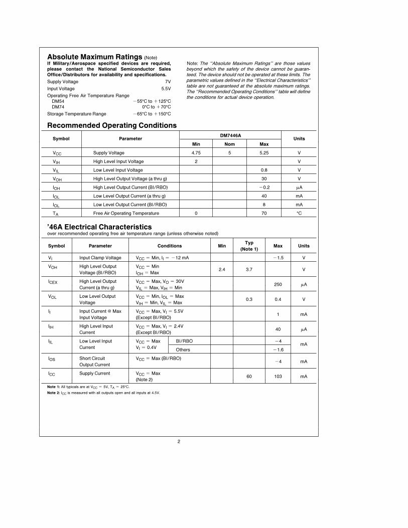
Absolute Maximum Ratings (Note)
If Military/Aerospace specified devices are required,
please contact the National Semiconductor Sales
Office/Distributors for availability and specifications.
Supply Voltage 7V
Input Voltage 5.5V
Operating Free Air Temperature Range
DM54 b55§C to a125§CDM74 0§C to a70§C
Storage Temperature Range b65§C to a150§C
Note: The ‘‘Absolute Maximum Ratings’’ are those valuesbeyond which the safety of the device cannot be guaran-teed. The device should not be operated at these limits. Theparametric values defined in the ‘‘Electrical Characteristics’’table are not guaranteed at the absolute maximum ratings.The ‘‘Recommended Operating Conditions’’ table will definethe conditions for actual device operation.
Recommended Operating Conditions
Symbol ParameterDM7446A
UnitsMin Nom Max
VCC Supply Voltage 4.75 5 5.25 V
VIH High Level Input Voltage 2 V
VIL Low Level Input Voltage 0.8 V
VOH High Level Output Voltage (a thru g) 30 V
IOH High Level Output Current (BI/RBO) b0.2 mA
IOL Low Level Output Current (a thru g) 40 mA
IOL Low Level Output Current (BI/RBO) 8 mA
TA Free Air Operating Temperature 0 70 §C
’46A Electrical Characteristicsover recommended operating free air temperature range (unless otherwise noted)
Symbol Parameter Conditions MinTyp
Max Units(Note 1)
VI Input Clamp Voltage VCC e Min, II e b12 mA b1.5 V
VOH High Level Output VCC e Min2.4 3.7 V
Voltage (BI/RBO) IOH e Max
ICEX High Level Output VCC e Max, VO e 30V250 mA
Current (a thru g) VIL e Max, VIH e Min
VOL Low Level Output VCC e Min, IOL e Max0.3 0.4 V
Voltage VIH e Min, VIL e Max
II Input Current @ Max VCC e Max, VI e 5.5V1 mA
Input Voltage (Except BI/RBO)
IIH High Level Input VCC e Max, VI e 2.4V40 mA
Current (Except BI/RBO)
IIL Low Level Input VCC e Max BI/RBO b4mA
Current VI e 0.4VOthers b1.6
IOS Short Circuit VCC e Max (BI/RBO)b4 mA
Output Current
ICC Supply Current VCC e Max60 103 mA
(Note 2)
Note 1: All typicals are at VCC e 5V, TA e 25§C.
Note 2: ICC is measured with all outputs open and all inputs at 4.5V.
2

’46A Switching Characteristicsat VCC e 5V and TA e 25§C (See Section 1 for Test Waveforms and Output Load)
Symbol Parameter Conditions Min Max Units
tPLH Propagation Delay Time CL e 15 pF100 ns
Low to High Level Output RL e 120X
tPHL Propagation Delay Time100 ns
High to Low Level Output
Recommended Operating Conditions
Symbol ParameterDM5447A DM7447A
UnitsMin Nom Max Min Nom Max
VCC Supply Voltage 4.5 5 5.5 4.75 5 5.25 V
VIH High Level Input Voltage 2 2 V
VIL Low Level Input Voltage 0.8 0.8 V
VOH High Level Output15 15 V
Voltage (a thru g)
IOH High Level Outputb0.2 b0.2 mA
Current (BI/RBO)
IOL Low Level Output40 40 mA
Current (a thru g)
IOL Low Level Output8 8 mA
Current (BI/RBO)
TA Free Air Operating Temperature b55 125 0 70 §C
’47A Electrical Characteristicsover recommended operating free air temperature range (unless otherwise noted)
Symbol Parameter Conditions MinTyp
Max Units(Note 1)
VI Input Clamp Voltage VCC e Min, II e b12 mA b1.5 V
VOH High Level Output VCC e Min2.4 3.7 V
Voltage (BI/RBO) IOH e Max
ICEX High Level Output VCC e Max, VO e 15V250 mA
Current (a thru g) VIL e Max, VIH e Min
VOL Low Level Output VCC e Min, IOL e Max0.3 0.4 V
Voltage VIH e Min, VIL e Max
II Input Current @ Max VCC e Max, VI e 5.5V1 mA
Input Voltage
IIH High Level Input Current VCC e Max, VI e 2.4V 40 mA
IIL Low Level Input VCC e Max BI/RBO b4mA
Current VI e 0.4VOthers b1.6
IOS Short Circuit VCC e Max (BI/RBO)b4 mA
Output Current
ICC Supply Current VCC e Max DM54 60 85mA
(Note 2)DM74 60 103
Note 1: All typicals are at VCC e 5V, TA e 25§C.
Note 2: ICC is measured with all outputs open and all inputs at 4.5V.
3

’47A Switching Characteristicsat VCC e 5V and TA e 25§C (See Section 1 for Test Waveforms and Output Load)
Symbol Parameter Conditions Min Max Units
tPLH Propagation Delay Time CL e 15 pF100 ns
Low to High Level Output RL e 120X
tPHL Propagation Delay Time100 ns
High to Low Level Output
Function Table46A, 47A
Decimal or Inputs BI/RBO OutputsNote
FunctionLT RBI D C B A
(Note 1)a b c d e f g
0 H H L L L L H L L L L L L H
1 H X L L L H H H L L H H H H
2 H X L L H L H L L H L L H L
3 H X L L H H H L L L L H H L
4 H X L H L L H H L L H H L L
5 H X L H L H H L H L L H L L
6 H X L H H L H H H L L L L L
7 H X L H H H H L L L H H H H(2)
8 H X H L L L H L L L L L L L
9 H X H L L H H L L L H H L L
10 H X H L H L H H H H L L H L
11 H X H L H H H H H L L H H L
12 H X H H L L H H L H H H L L
13 H X H H L H H L H H L H L L
14 H X H H H L H H H H L L L L
15 H X H H H H H H H H H H H H
BI X X X X X X L H H H H H H H (3)
RBI H L L L L L L H H H H H H H (4)
LT L X X X X X H L L L L L L L (5)
Note 1: BI/RBO is a wire-AND logic serving as blanking input (BI) and/or ripple-blanking output (RBO).
Note 2: The blanking input (BI) must be open or held at a high logic level when output functions 0 through 15 are desired. The ripple-blanking input (RBI) must
be open or high if blanking of a decimal zero is not desired.
Note 3: When a low logic level is applied directly to the blanking input (BI), all segment outputs are high regardless of the level of any other input.
Note 4: When ripple-blanking input (RBI) and inputs A, B, C, and D are at a low level with the lamp test input high, all segment outputs go H and the ripple-
blanking output (RBO) goes to a low level (response condition).
Note 5: When the blanking input/ripple-blanking output (BI/RBO) is open or held high and a low is applied to the lamp-test input, all segment outputs are L .
H e High level, L e Low level, X e Don’t Care
4

Logic Diagram
TL/F/6518–2
Physical Dimensions inches (millimeters)
16-Lead Ceramic Dual-In-Line Package (J)
Order Number DM5447AJ
NS Package Number J16A
5

DM
7446A
,D
M5447A
/D
M7447A
BC
Dto
7-S
egm
entD
ecoders
/D
rivers
Physical Dimensions inches (millimeters) (Continued)
16-Lead Molded Dual-In-Line Package (N)
Order Number DM7446AN or DM7447AN
NS Package Number N16E
LIFE SUPPORT POLICY
NATIONAL’S PRODUCTS ARE NOT AUTHORIZED FOR USE AS CRITICAL COMPONENTS IN LIFE SUPPORT
DEVICES OR SYSTEMS WITHOUT THE EXPRESS WRITTEN APPROVAL OF THE PRESIDENT OF NATIONAL
SEMICONDUCTOR CORPORATION. As used herein:
1. Life support devices or systems are devices or 2. A critical component is any component of a life
systems which, (a) are intended for surgical implant support device or system whose failure to perform can
into the body, or (b) support or sustain life, and whose be reasonably expected to cause the failure of the life
failure to perform, when properly used in accordance support device or system, or to affect its safety or
with instructions for use provided in the labeling, can effectiveness.
be reasonably expected to result in a significant injury
to the user.
National Semiconductor National Semiconductor National Semiconductor National SemiconductorCorporation Europe Hong Kong Ltd. Japan Ltd.1111 West Bardin Road Fax: (a49) 0-180-530 85 86 13th Floor, Straight Block, Tel: 81-043-299-2309Arlington, TX 76017 Email: cnjwge@ tevm2.nsc.com Ocean Centre, 5 Canton Rd. Fax: 81-043-299-2408Tel: 1(800) 272-9959 Deutsch Tel: (a49) 0-180-530 85 85 Tsimshatsui, KowloonFax: 1(800) 737-7018 English Tel: (a49) 0-180-532 78 32 Hong Kong
Fran3ais Tel: (a49) 0-180-532 93 58 Tel: (852) 2737-1600Italiano Tel: (a49) 0-180-534 16 80 Fax: (852) 2736-9960
National does not assume any responsibility for use of any circuitry described, no circuit patent licenses are implied and National reserves the right at any time without notice to change said circuitry and specifications.

SN5474, SN54LS74A, SN54S74SN7474. SN74LS74A, SN74S74
DUAL D-TYPE POSITIVE-EDGE-TRIGGERED FLIP-FLOPS WITH PRESET AND CLEAR
SDLS119 – DECEMBER 1983 – REVISED MARCH 1988
1POST OFFICE BOX 655303 • DALLAS, TEXAS 75265
Copyright 1988, Texas Instruments IncorporatedPRODUCTION DATA information is current as of publication date.Products conform to specifications per the terms of Texas Instrumentsstandard warranty. Production processing does not necessarily includetesting of all parameters.

SN5474, SN54LS74A, SN54S74SN7474. SN74LS74A, SN74S74DUAL D-TYPE POSITIVE-EDGE-TRIGGERED FLIP-FLOPS WITH PRESET AND CLEAR
SDLS119 – DECEMBER 1983 – REVISED MARCH 1988
2 POST OFFICE BOX 655303 • DALLAS, TEXAS 75265

SN5474, SN54LS74A, SN54S74SN7474. SN74LS74A, SN74S74
DUAL D-TYPE POSITIVE-EDGE-TRIGGERED FLIP-FLOPS WITH PRESET AND CLEAR
SDLS119 – DECEMBER 1983 – REVISED MARCH 1988
3POST OFFICE BOX 655303 • DALLAS, TEXAS 75265

SN5474, SN54LS74A, SN54S74SN7474. SN74LS74A, SN74S74DUAL D-TYPE POSITIVE-EDGE-TRIGGERED FLIP-FLOPS WITH PRESET AND CLEAR
SDLS119 – DECEMBER 1983 – REVISED MARCH 1988
4 POST OFFICE BOX 655303 • DALLAS, TEXAS 75265

SN5474, SN54LS74A, SN54S74SN7474. SN74LS74A, SN74S74
DUAL D-TYPE POSITIVE-EDGE-TRIGGERED FLIP-FLOPS WITH PRESET AND CLEAR
SDLS119 – DECEMBER 1983 – REVISED MARCH 1988
5POST OFFICE BOX 655303 • DALLAS, TEXAS 75265

SN5474, SN54LS74A, SN54S74SN7474. SN74LS74A, SN74S74DUAL D-TYPE POSITIVE-EDGE-TRIGGERED FLIP-FLOPS WITH PRESET AND CLEAR
SDLS119 – DECEMBER 1983 – REVISED MARCH 1988
6 POST OFFICE BOX 655303 • DALLAS, TEXAS 75265

PACKAGING INFORMATION
Orderable Device Status (1) PackageType
PackageDrawing
Pins PackageQty
Eco Plan (2) Lead/Ball Finish MSL Peak Temp (3)
JM38510/00205BCA OBSOLETE CDIP J 14 TBD Call TI Call TI
JM38510/00205BDA OBSOLETE CFP W 14 TBD Call TI Call TI
JM38510/00205BDA OBSOLETE CFP W 14 TBD Call TI Call TI
JM38510/07101BCA ACTIVE CDIP J 14 1 TBD Call TI Level-NC-NC-NC
JM38510/07101BCA ACTIVE CDIP J 14 1 TBD Call TI Level-NC-NC-NC
JM38510/07101BDA ACTIVE CFP W 14 1 TBD Call TI Level-NC-NC-NC
JM38510/07101BDA ACTIVE CFP W 14 1 TBD Call TI Level-NC-NC-NC
JM38510/30102B2A ACTIVE LCCC FK 20 1 TBD Call TI Level-NC-NC-NC
JM38510/30102B2A ACTIVE LCCC FK 20 1 TBD Call TI Level-NC-NC-NC
JM38510/30102BCA ACTIVE CDIP J 14 1 TBD Call TI Level-NC-NC-NC
JM38510/30102BCA ACTIVE CDIP J 14 1 TBD Call TI Level-NC-NC-NC
JM38510/30102BDA ACTIVE CFP W 14 1 TBD Call TI Level-NC-NC-NC
JM38510/30102BDA ACTIVE CFP W 14 1 TBD Call TI Level-NC-NC-NC
JM38510/30102SCA ACTIVE CDIP J 14 1 TBD Call TI Level-NC-NC-NC
JM38510/30102SCA ACTIVE CDIP J 14 1 TBD Call TI Level-NC-NC-NC
JM38510/30102SDA ACTIVE CFP W 14 1 TBD Call TI Level-NC-NC-NC
JM38510/30102SDA ACTIVE CFP W 14 1 TBD Call TI Level-NC-NC-NC
SN5474J OBSOLETE CDIP J 14 TBD Call TI Call TI
SN5474J OBSOLETE CDIP J 14 TBD Call TI Call TI
SN54LS74AJ ACTIVE CDIP J 14 1 TBD Call TI Level-NC-NC-NC
SN54LS74AJ ACTIVE CDIP J 14 1 TBD Call TI Level-NC-NC-NC
SN54S74J ACTIVE CDIP J 14 1 TBD Call TI Level-NC-NC-NC
SN54S74J ACTIVE CDIP J 14 1 TBD Call TI Level-NC-NC-NC
SN7474DR OBSOLETE SOIC D 14 TBD Call TI Call TI
SN7474DR OBSOLETE SOIC D 14 TBD Call TI Call TI
SN7474N OBSOLETE PDIP N 14 TBD Call TI Call TI
SN7474N OBSOLETE PDIP N 14 TBD Call TI Call TI
SN7474N3 OBSOLETE PDIP N 14 TBD Call TI Call TI
SN7474N3 OBSOLETE PDIP N 14 TBD Call TI Call TI
SN74LS74AD ACTIVE SOIC D 14 50 Green (RoHS &no Sb/Br)
CU NIPDAU Level-1-260C-UNLIM
SN74LS74AD ACTIVE SOIC D 14 50 Green (RoHS &no Sb/Br)
CU NIPDAU Level-1-260C-UNLIM
SN74LS74ADBR ACTIVE SSOP DB 14 2000 Green (RoHS &no Sb/Br)
CU NIPDAU Level-1-260C-UNLIM
SN74LS74ADBR ACTIVE SSOP DB 14 2000 Green (RoHS &no Sb/Br)
CU NIPDAU Level-1-260C-UNLIM
SN74LS74ADBRE4 ACTIVE SSOP DB 14 2000 Green (RoHS &no Sb/Br)
CU NIPDAU Level-1-260C-UNLIM
SN74LS74ADBRE4 ACTIVE SSOP DB 14 2000 Green (RoHS &no Sb/Br)
CU NIPDAU Level-1-260C-UNLIM
SN74LS74ADE4 ACTIVE SOIC D 14 50 Green (RoHS &no Sb/Br)
CU NIPDAU Level-1-260C-UNLIM
SN74LS74ADE4 ACTIVE SOIC D 14 50 Green (RoHS & CU NIPDAU Level-1-260C-UNLIM
PACKAGE OPTION ADDENDUM
www.ti.com 17-Oct-2005
Addendum-Page 1

Orderable Device Status (1) PackageType
PackageDrawing
Pins PackageQty
Eco Plan (2) Lead/Ball Finish MSL Peak Temp (3)
no Sb/Br)
SN74LS74ADR ACTIVE SOIC D 14 2500 Green (RoHS &no Sb/Br)
CU NIPDAU Level-1-260C-UNLIM
SN74LS74ADR ACTIVE SOIC D 14 2500 Green (RoHS &no Sb/Br)
CU NIPDAU Level-1-260C-UNLIM
SN74LS74ADRE4 ACTIVE SOIC D 14 2500 Green (RoHS &no Sb/Br)
CU NIPDAU Level-1-260C-UNLIM
SN74LS74ADRE4 ACTIVE SOIC D 14 2500 Green (RoHS &no Sb/Br)
CU NIPDAU Level-1-260C-UNLIM
SN74LS74AJ OBSOLETE CDIP J 14 TBD Call TI Call TI
SN74LS74AJ OBSOLETE CDIP J 14 TBD Call TI Call TI
SN74LS74AN ACTIVE PDIP N 14 25 Pb-Free(RoHS)
CU NIPDAU Level-NC-NC-NC
SN74LS74AN ACTIVE PDIP N 14 25 Pb-Free(RoHS)
CU NIPDAU Level-NC-NC-NC
SN74LS74AN3 OBSOLETE PDIP N 14 TBD Call TI Call TI
SN74LS74AN3 OBSOLETE PDIP N 14 TBD Call TI Call TI
SN74LS74ANE4 ACTIVE PDIP N 14 25 Pb-Free(RoHS)
CU NIPDAU Level-NC-NC-NC
SN74LS74ANE4 ACTIVE PDIP N 14 25 Pb-Free(RoHS)
CU NIPDAU Level-NC-NC-NC
SN74LS74ANSR ACTIVE SO NS 14 2000 Green (RoHS &no Sb/Br)
CU NIPDAU Level-1-260C-UNLIM
SN74LS74ANSR ACTIVE SO NS 14 2000 Green (RoHS &no Sb/Br)
CU NIPDAU Level-1-260C-UNLIM
SN74LS74ANSRG4 ACTIVE SO NS 14 2000 Green (RoHS &no Sb/Br)
CU NIPDAU Level-1-260C-UNLIM
SN74LS74ANSRG4 ACTIVE SO NS 14 2000 Green (RoHS &no Sb/Br)
CU NIPDAU Level-1-260C-UNLIM
SN74S74D ACTIVE SOIC D 14 50 Green (RoHS &no Sb/Br)
CU NIPDAU Level-1-260C-UNLIM
SN74S74D ACTIVE SOIC D 14 50 Green (RoHS &no Sb/Br)
CU NIPDAU Level-1-260C-UNLIM
SN74S74DE4 ACTIVE SOIC D 14 50 Green (RoHS &no Sb/Br)
CU NIPDAU Level-1-260C-UNLIM
SN74S74DE4 ACTIVE SOIC D 14 50 Green (RoHS &no Sb/Br)
CU NIPDAU Level-1-260C-UNLIM
SN74S74DR ACTIVE SOIC D 14 2500 Green (RoHS &no Sb/Br)
CU NIPDAU Level-1-260C-UNLIM
SN74S74DR ACTIVE SOIC D 14 2500 Green (RoHS &no Sb/Br)
CU NIPDAU Level-1-260C-UNLIM
SN74S74DRE4 ACTIVE SOIC D 14 2500 Green (RoHS &no Sb/Br)
CU NIPDAU Level-1-260C-UNLIM
SN74S74DRE4 ACTIVE SOIC D 14 2500 Green (RoHS &no Sb/Br)
CU NIPDAU Level-1-260C-UNLIM
SN74S74N ACTIVE PDIP N 14 25 Pb-Free(RoHS)
CU NIPDAU Level-NC-NC-NC
SN74S74N ACTIVE PDIP N 14 25 Pb-Free(RoHS)
CU NIPDAU Level-NC-NC-NC
SN74S74N3 OBSOLETE PDIP N 14 TBD Call TI Call TI
PACKAGE OPTION ADDENDUM
www.ti.com 17-Oct-2005
Addendum-Page 2

Orderable Device Status (1) PackageType
PackageDrawing
Pins PackageQty
Eco Plan (2) Lead/Ball Finish MSL Peak Temp (3)
SN74S74N3 OBSOLETE PDIP N 14 TBD Call TI Call TI
SN74S74NE4 ACTIVE PDIP N 14 25 Pb-Free(RoHS)
CU NIPDAU Level-NC-NC-NC
SN74S74NE4 ACTIVE PDIP N 14 25 Pb-Free(RoHS)
CU NIPDAU Level-NC-NC-NC
SN74S74NSR ACTIVE SO NS 14 2000 Green (RoHS &no Sb/Br)
CU NIPDAU Level-1-260C-UNLIM
SN74S74NSR ACTIVE SO NS 14 2000 Green (RoHS &no Sb/Br)
CU NIPDAU Level-1-260C-UNLIM
SN74S74NSRE4 ACTIVE SO NS 14 2000 Green (RoHS &no Sb/Br)
CU NIPDAU Level-1-260C-UNLIM
SN74S74NSRE4 ACTIVE SO NS 14 2000 Green (RoHS &no Sb/Br)
CU NIPDAU Level-1-260C-UNLIM
SNJ5474J OBSOLETE CDIP J 14 TBD Call TI Call TI
SNJ5474J OBSOLETE CDIP J 14 TBD Call TI Call TI
SNJ5474W OBSOLETE CFP W 14 TBD Call TI Call TI
SNJ5474W OBSOLETE CFP W 14 TBD Call TI Call TI
SNJ54LS74AFK ACTIVE LCCC FK 20 1 TBD Call TI Level-NC-NC-NC
SNJ54LS74AFK ACTIVE LCCC FK 20 1 TBD Call TI Level-NC-NC-NC
SNJ54LS74AJ ACTIVE CDIP J 14 1 TBD Call TI Level-NC-NC-NC
SNJ54LS74AJ ACTIVE CDIP J 14 1 TBD Call TI Level-NC-NC-NC
SNJ54LS74AW ACTIVE CFP W 14 1 TBD Call TI Level-NC-NC-NC
SNJ54LS74AW ACTIVE CFP W 14 1 TBD Call TI Level-NC-NC-NC
SNJ54S74FK ACTIVE LCCC FK 20 1 TBD Call TI Level-NC-NC-NC
SNJ54S74FK ACTIVE LCCC FK 20 1 TBD Call TI Level-NC-NC-NC
SNJ54S74J ACTIVE CDIP J 14 1 TBD Call TI Level-NC-NC-NC
SNJ54S74J ACTIVE CDIP J 14 1 TBD Call TI Level-NC-NC-NC
SNJ54S74W ACTIVE CFP W 14 1 TBD Call TI Level-NC-NC-NC
SNJ54S74W ACTIVE CFP W 14 1 TBD Call TI Level-NC-NC-NC
(1) The marketing status values are defined as follows:ACTIVE: Product device recommended for new designs.LIFEBUY: TI has announced that the device will be discontinued, and a lifetime-buy period is in effect.NRND: Not recommended for new designs. Device is in production to support existing customers, but TI does not recommend using this part ina new design.PREVIEW: Device has been announced but is not in production. Samples may or may not be available.OBSOLETE: TI has discontinued the production of the device.
(2) Eco Plan - The planned eco-friendly classification: Pb-Free (RoHS) or Green (RoHS & no Sb/Br) - please checkhttp://www.ti.com/productcontent for the latest availability information and additional product content details.TBD: The Pb-Free/Green conversion plan has not been defined.Pb-Free (RoHS): TI's terms "Lead-Free" or "Pb-Free" mean semiconductor products that are compatible with the current RoHS requirementsfor all 6 substances, including the requirement that lead not exceed 0.1% by weight in homogeneous materials. Where designed to be solderedat high temperatures, TI Pb-Free products are suitable for use in specified lead-free processes.Green (RoHS & no Sb/Br): TI defines "Green" to mean Pb-Free (RoHS compatible), and free of Bromine (Br) and Antimony (Sb) based flameretardants (Br or Sb do not exceed 0.1% by weight in homogeneous material)
(3) MSL, Peak Temp. -- The Moisture Sensitivity Level rating according to the JEDEC industry standard classifications, and peak soldertemperature.
Important Information and Disclaimer:The information provided on this page represents TI's knowledge and belief as of the date that it is
PACKAGE OPTION ADDENDUM
www.ti.com 17-Oct-2005
Addendum-Page 3

provided. TI bases its knowledge and belief on information provided by third parties, and makes no representation or warranty as to theaccuracy of such information. Efforts are underway to better integrate information from third parties. TI has taken and continues to takereasonable steps to provide representative and accurate information but may not have conducted destructive testing or chemical analysis onincoming materials and chemicals. TI and TI suppliers consider certain information to be proprietary, and thus CAS numbers and other limitedinformation may not be available for release.
In no event shall TI's liability arising out of such information exceed the total purchase price of the TI part(s) at issue in this document sold by TIto Customer on an annual basis.
PACKAGE OPTION ADDENDUM
www.ti.com 17-Oct-2005
Addendum-Page 4


MECHANICAL DATA
MLCC006B – OCTOBER 1996
POST OFFICE BOX 655303 • DALLAS, TEXAS 75265
FK (S-CQCC-N**) LEADLESS CERAMIC CHIP CARRIER
4040140/D 10/96
28 TERMINAL SHOWN
B
0.358(9,09)
MAX
(11,63)
0.560(14,22)
0.560
0.458
0.858(21,8)
1.063(27,0)
(14,22)
ANO. OF
MINMAX
0.358
0.660
0.761
0.458
0.342(8,69)
MIN
(11,23)
(16,26)0.640
0.739
0.442
(9,09)
(11,63)
(16,76)
0.962
1.165
(23,83)0.938
(28,99)1.141
(24,43)
(29,59)
(19,32)(18,78)
**
20
28
52
44
68
84
0.020 (0,51)
TERMINALS
0.080 (2,03)0.064 (1,63)
(7,80)0.307
(10,31)0.406
(12,58)0.495
(12,58)0.495
(21,6)0.850
(26,6)1.047
0.045 (1,14)
0.045 (1,14)0.035 (0,89)
0.035 (0,89)
0.010 (0,25)
121314151618 17
11
10
8
9
7
5
432
0.020 (0,51)0.010 (0,25)
6
12826 27
19
21B SQ
A SQ22
23
24
25
20
0.055 (1,40)0.045 (1,14)
0.028 (0,71)0.022 (0,54)
0.050 (1,27)
NOTES: A. All linear dimensions are in inches (millimeters).B. This drawing is subject to change without notice.C. This package can be hermetically sealed with a metal lid.D. The terminals are gold plated.E. Falls within JEDEC MS-004


MECHANICAL DATA
MSSO002E – JANUARY 1995 – REVISED DECEMBER 2001
POST OFFICE BOX 655303 • DALLAS, TEXAS 75265
DB (R-PDSO-G**) PLASTIC SMALL-OUTLINE
4040065 /E 12/01
28 PINS SHOWN
Gage Plane
8,207,40
0,550,95
0,25
38
12,90
12,30
28
10,50
24
8,50
Seating Plane
9,907,90
30
10,50
9,90
0,38
5,605,00
15
0,22
14
A
28
1
2016
6,506,50
14
0,05 MIN
5,905,90
DIM
A MAX
A MIN
PINS **
2,00 MAX
6,90
7,50
0,65 M0,15
0°–8°
0,10
0,090,25
NOTES: A. All linear dimensions are in millimeters.B. This drawing is subject to change without notice.C. Body dimensions do not include mold flash or protrusion not to exceed 0,15.D. Falls within JEDEC MO-150

IMPORTANT NOTICE
Texas Instruments Incorporated and its subsidiaries (TI) reserve the right to make corrections, modifications,enhancements, improvements, and other changes to its products and services at any time and to discontinueany product or service without notice. Customers should obtain the latest relevant information before placingorders and should verify that such information is current and complete. All products are sold subject to TI’s termsand conditions of sale supplied at the time of order acknowledgment.
TI warrants performance of its hardware products to the specifications applicable at the time of sale inaccordance with TI’s standard warranty. Testing and other quality control techniques are used to the extent TIdeems necessary to support this warranty. Except where mandated by government requirements, testing of allparameters of each product is not necessarily performed.
TI assumes no liability for applications assistance or customer product design. Customers are responsible fortheir products and applications using TI components. To minimize the risks associated with customer productsand applications, customers should provide adequate design and operating safeguards.
TI does not warrant or represent that any license, either express or implied, is granted under any TI patent right,copyright, mask work right, or other TI intellectual property right relating to any combination, machine, or processin which TI products or services are used. Information published by TI regarding third-party products or servicesdoes not constitute a license from TI to use such products or services or a warranty or endorsement thereof.Use of such information may require a license from a third party under the patents or other intellectual propertyof the third party, or a license from TI under the patents or other intellectual property of TI.
Reproduction of information in TI data books or data sheets is permissible only if reproduction is withoutalteration and is accompanied by all associated warranties, conditions, limitations, and notices. Reproductionof this information with alteration is an unfair and deceptive business practice. TI is not responsible or liable forsuch altered documentation.
Resale of TI products or services with statements different from or beyond the parameters stated by TI for thatproduct or service voids all express and any implied warranties for the associated TI product or service andis an unfair and deceptive business practice. TI is not responsible or liable for any such statements.
Following are URLs where you can obtain information on other Texas Instruments products and applicationsolutions:
Products Applications
Amplifiers amplifier.ti.com Audio www.ti.com/audio
Data Converters dataconverter.ti.com Automotive www.ti.com/automotive
DSP dsp.ti.com Broadband www.ti.com/broadband
Interface interface.ti.com Digital Control www.ti.com/digitalcontrol
Logic logic.ti.com Military www.ti.com/military
Power Mgmt power.ti.com Optical Networking www.ti.com/opticalnetwork
Microcontrollers microcontroller.ti.com Security www.ti.com/security
Telephony www.ti.com/telephony
Video & Imaging www.ti.com/video
Wireless www.ti.com/wireless
Mailing Address: Texas Instruments
Post Office Box 655303 Dallas, Texas 75265
Copyright 2005, Texas Instruments Incorporated

SN5476, SN54LS76ASN7476, SN74LS76A
DUAL J-K FLIP-FLOPS WITH PRESET AND CLEAR
SDLS121 – DECEMBER 1983 – REVISED MARCH 1988
1POST OFFICE BOX 655303 • DALLAS, TEXAS 75265
Copyright 1988, Texas Instruments IncorporatedPRODUCTION DATA information is current as of publication date.Products conform to specifications per the terms of Texas Instrumentsstandard warranty. Production processing does not necessarily includetesting of all parameters.

SN5476, SN54LS76ASN7476, SN74LS76ADUAL J-K FLIP-FLOPS WITH PRESET AND CLEAR
SDLS121 – DECEMBER 1983 – REVISED MARCH 1988
2 POST OFFICE BOX 655303 • DALLAS, TEXAS 75265

SN5476, SN54LS76ASN7476, SN74LS76A
DUAL J-K FLIP-FLOPS WITH PRESET AND CLEAR
SDLS121 – DECEMBER 1983 – REVISED MARCH 1988
3POST OFFICE BOX 655303 • DALLAS, TEXAS 75265

SN5476, SN54LS76ASN7476, SN74LS76ADUAL J-K FLIP-FLOPS WITH PRESET AND CLEAR
SDLS121 – DECEMBER 1983 – REVISED MARCH 1988
4 POST OFFICE BOX 655303 • DALLAS, TEXAS 75265

SN5476, SN54LS76ASN7476, SN74LS76A
DUAL J-K FLIP-FLOPS WITH PRESET AND CLEAR
SDLS121 – DECEMBER 1983 – REVISED MARCH 1988
5POST OFFICE BOX 655303 • DALLAS, TEXAS 75265

SN5476, SN54LS76ASN7476, SN74LS76ADUAL J-K FLIP-FLOPS WITH PRESET AND CLEAR
SDLS121 – DECEMBER 1983 – REVISED MARCH 1988
6 POST OFFICE BOX 655303 • DALLAS, TEXAS 75265

PACKAGING INFORMATION
Orderable Device Status (1) PackageType
PackageDrawing
Pins PackageQty
Eco Plan (2) Lead/Ball Finish MSL Peak Temp (3)
5962-9557501QEA ACTIVE CDIP J 16 1 TBD Call TI Level-NC-NC-NC
5962-9557501QFA ACTIVE CFP W 16 1 TBD Call TI Level-NC-NC-NC
5962-9557501QFA ACTIVE CFP W 16 1 TBD Call TI Level-NC-NC-NC
7601301EA ACTIVE CDIP J 16 1 TBD Call TI Level-NC-NC-NC
7601301EA ACTIVE CDIP J 16 1 TBD Call TI Level-NC-NC-NC
JM38510/00204BEA ACTIVE CDIP J 16 1 TBD Call TI Level-NC-NC-NC
JM38510/00204BEA ACTIVE CDIP J 16 1 TBD Call TI Level-NC-NC-NC
SN5476J ACTIVE CDIP J 16 1 TBD Call TI Level-NC-NC-NC
SN5476J ACTIVE CDIP J 16 1 TBD Call TI Level-NC-NC-NC
SN54LS76AJ ACTIVE CDIP J 16 1 TBD Call TI Level-NC-NC-NC
SN54LS76AJ ACTIVE CDIP J 16 1 TBD Call TI Level-NC-NC-NC
SN7476N OBSOLETE PDIP N 16 TBD Call TI Call TI
SN7476N OBSOLETE PDIP N 16 TBD Call TI Call TI
SN7476N3 OBSOLETE PDIP N 16 TBD Call TI Call TI
SN7476N3 OBSOLETE PDIP N 16 TBD Call TI Call TI
SN74LS76AD OBSOLETE SOIC D 16 TBD Call TI Call TI
SN74LS76AD OBSOLETE SOIC D 16 TBD Call TI Call TI
SN74LS76ADR OBSOLETE SOIC D 16 TBD Call TI Call TI
SN74LS76ADR OBSOLETE SOIC D 16 TBD Call TI Call TI
SN74LS76AN OBSOLETE PDIP N 16 TBD Call TI Call TI
SN74LS76AN OBSOLETE PDIP N 16 TBD Call TI Call TI
SN74LS76AN3 OBSOLETE PDIP N 16 TBD Call TI Call TI
SN74LS76AN3 OBSOLETE PDIP N 16 TBD Call TI Call TI
SNJ5476J ACTIVE CDIP J 16 1 TBD Call TI Level-NC-NC-NC
SNJ5476J ACTIVE CDIP J 16 1 TBD Call TI Level-NC-NC-NC
SNJ5476W ACTIVE CFP W 16 1 TBD Call TI Level-NC-NC-NC
SNJ5476W ACTIVE CFP W 16 1 TBD Call TI Level-NC-NC-NC
SNJ54LS76AJ ACTIVE CDIP J 16 1 TBD Call TI Level-NC-NC-NC
SNJ54LS76AJ ACTIVE CDIP J 16 1 TBD Call TI Level-NC-NC-NC
SNJ54LS76AW ACTIVE CFP W 16 1 TBD Call TI Level-NC-NC-NC
SNJ54LS76AW ACTIVE CFP W 16 1 TBD Call TI Level-NC-NC-NC
(1) The marketing status values are defined as follows:ACTIVE: Product device recommended for new designs.LIFEBUY: TI has announced that the device will be discontinued, and a lifetime-buy period is in effect.NRND: Not recommended for new designs. Device is in production to support existing customers, but TI does not recommend using this part ina new design.PREVIEW: Device has been announced but is not in production. Samples may or may not be available.OBSOLETE: TI has discontinued the production of the device.
(2) Eco Plan - The planned eco-friendly classification: Pb-Free (RoHS) or Green (RoHS & no Sb/Br) - please checkhttp://www.ti.com/productcontent for the latest availability information and additional product content details.TBD: The Pb-Free/Green conversion plan has not been defined.Pb-Free (RoHS): TI's terms "Lead-Free" or "Pb-Free" mean semiconductor products that are compatible with the current RoHS requirementsfor all 6 substances, including the requirement that lead not exceed 0.1% by weight in homogeneous materials. Where designed to be solderedat high temperatures, TI Pb-Free products are suitable for use in specified lead-free processes.
PACKAGE OPTION ADDENDUM
www.ti.com 26-Sep-2005
Addendum-Page 1

Green (RoHS & no Sb/Br): TI defines "Green" to mean Pb-Free (RoHS compatible), and free of Bromine (Br) and Antimony (Sb) based flameretardants (Br or Sb do not exceed 0.1% by weight in homogeneous material)
(3) MSL, Peak Temp. -- The Moisture Sensitivity Level rating according to the JEDEC industry standard classifications, and peak soldertemperature.
Important Information and Disclaimer:The information provided on this page represents TI's knowledge and belief as of the date that it isprovided. TI bases its knowledge and belief on information provided by third parties, and makes no representation or warranty as to theaccuracy of such information. Efforts are underway to better integrate information from third parties. TI has taken and continues to takereasonable steps to provide representative and accurate information but may not have conducted destructive testing or chemical analysis onincoming materials and chemicals. TI and TI suppliers consider certain information to be proprietary, and thus CAS numbers and other limitedinformation may not be available for release.
In no event shall TI's liability arising out of such information exceed the total purchase price of the TI part(s) at issue in this document sold by TIto Customer on an annual basis.
PACKAGE OPTION ADDENDUM
www.ti.com 26-Sep-2005
Addendum-Page 2

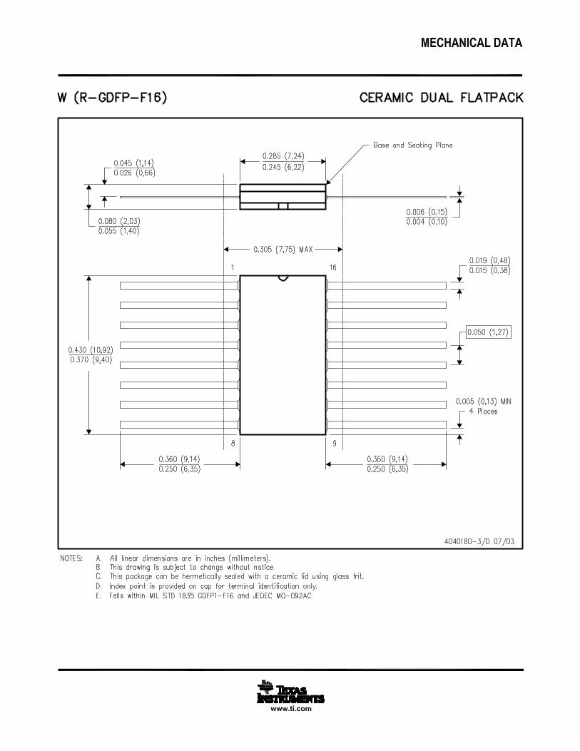

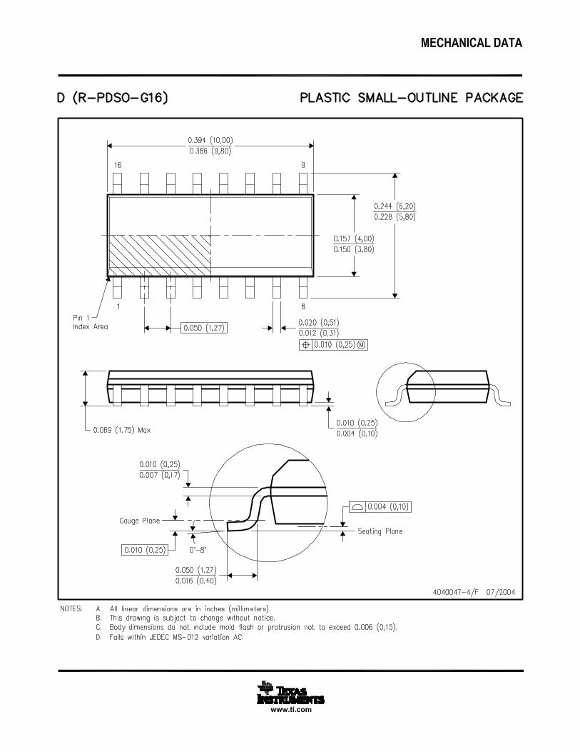
IMPORTANT NOTICE
Texas Instruments Incorporated and its subsidiaries (TI) reserve the right to make corrections, modifications,enhancements, improvements, and other changes to its products and services at any time and to discontinueany product or service without notice. Customers should obtain the latest relevant information before placingorders and should verify that such information is current and complete. All products are sold subject to TI’s termsand conditions of sale supplied at the time of order acknowledgment.
TI warrants performance of its hardware products to the specifications applicable at the time of sale inaccordance with TI’s standard warranty. Testing and other quality control techniques are used to the extent TIdeems necessary to support this warranty. Except where mandated by government requirements, testing of allparameters of each product is not necessarily performed.
TI assumes no liability for applications assistance or customer product design. Customers are responsible fortheir products and applications using TI components. To minimize the risks associated with customer productsand applications, customers should provide adequate design and operating safeguards.
TI does not warrant or represent that any license, either express or implied, is granted under any TI patent right,copyright, mask work right, or other TI intellectual property right relating to any combination, machine, or processin which TI products or services are used. Information published by TI regarding third-party products or servicesdoes not constitute a license from TI to use such products or services or a warranty or endorsement thereof.Use of such information may require a license from a third party under the patents or other intellectual propertyof the third party, or a license from TI under the patents or other intellectual property of TI.
Reproduction of information in TI data books or data sheets is permissible only if reproduction is withoutalteration and is accompanied by all associated warranties, conditions, limitations, and notices. Reproductionof this information with alteration is an unfair and deceptive business practice. TI is not responsible or liable forsuch altered documentation.
Resale of TI products or services with statements different from or beyond the parameters stated by TI for thatproduct or service voids all express and any implied warranties for the associated TI product or service andis an unfair and deceptive business practice. TI is not responsible or liable for any such statements.
Following are URLs where you can obtain information on other Texas Instruments products and applicationsolutions:
Products Applications
Amplifiers amplifier.ti.com Audio www.ti.com/audio
Data Converters dataconverter.ti.com Automotive www.ti.com/automotive
DSP dsp.ti.com Broadband www.ti.com/broadband
Interface interface.ti.com Digital Control www.ti.com/digitalcontrol
Logic logic.ti.com Military www.ti.com/military
Power Mgmt power.ti.com Optical Networking www.ti.com/opticalnetwork
Microcontrollers microcontroller.ti.com Security www.ti.com/security
Telephony www.ti.com/telephony
Video & Imaging www.ti.com/video
Wireless www.ti.com/wireless
Mailing Address: Texas Instruments
Post Office Box 655303 Dallas, Texas 75265
Copyright 2005, Texas Instruments Incorporated


© 2000 Fairchild Semiconductor Corporation DS006531 www.fairchildsemi.com
September 1986
Revised February 2000
DM
7486 Qu
ad 2-In
pu
t Exclu
sive-OR
Gate
DM7486 Quad 2-Input Exclusive-OR Gate
General DescriptionThis device contains four independent gates each of whichperforms the logic exclusive-OR function.
Ordering Code:
Connection Diagram Function TableY = A ⊕ B
H = HIGH Logic LevelL = LOW Logic Level
Order Number Package Number Package Description
DM7486N N14A 14-Lead Plastic Dual-In-Line Package (PDIP), JEDEC MS-001, 0.300 Wide
Inputs Output
A B Y
L L L
L H H
H L H
H H L

www.fairchildsemi.com 2
DM
7486 Absolute Maximum Ratings(Note 1)
Note 1: The “Absolute Maximum Ratings” are those values beyond whichthe safety of the device cannot be guaranteed. The device should not beoperated at these limits. The parametric values defined in the ElectricalCharacteristics tables are not guaranteed at the absolute maximum ratings.The “Recommended Operating Conditions” table will define the conditionsfor actual device operation.
Recommended Operating Conditions
Electrical Characteristicsover recommended operating free air temperature range (unless otherwise noted)
Note 2: All typicals are at VCC = 5V, TA = 25°C.
Note 3: Not more than one output should be shorted at a time.
Note 4: ICCH is measured with all outputs open, one input of each gate at 4.5V, and the other inputs grounded.
Note 5: ICCL is measured with all outputs open, and all inputs at ground.
Switching Characteristics at VCC = 5V and TA = 25°C
Supply Voltage 7V
Input Voltage 5.5V
Operating Free Air Temperature Range 0°C to +70°C
Storage Temperature Range −65°C to +150°C
Symbol Parameter Min Nom Max Units
VCC Supply Voltage 4.75 5 5.25 V
VIH HIGH Level Input Voltage 2 V
VIL LOW Level Input Voltage 0.8 V
IOH HIGH Level Output Current −0.8 mA
IOL LOW Level Output Current 16 mA
TA Free Air Operating Temperature 0 70 °C
Symbol Parameter Conditions MinTyp
Max Units(Note 2)
VI Input Clamp Voltage VCC = Min, II = −12 mA −1.5 V
VOH HIGH Level VCC = Min, IOH = Max2.4 3.4 V
Output Voltage VIL = Max, VIH = Min
VOL LOW Level VCC = Min, IOL = Max0.2 0.4 V
Output Voltage VIH = Min, VIL = Max
II Input Current @ Max Input Voltage VCC = Max, VI = 5.5V 1 mA
IIH HIGH Level Input Current VCC = Max, VI = 2.4V 40 µA
IIL LOW Level Input Current VCC = Max, VI = 0.4V −1.6 mA
IOS Short Circuit Output Current VCC = Max (Note 3) −18 −55 mA
ICCH Supply Current with Outputs HIGH VCC = Max (Note 4) 30 50 mA
ICCL Supply Current with Outputs LOW VCC = Max (Note 3)(Note 5) 36 57 mA
Symbol Parameter ConditionsCL = 15 pF, RL = 400Ω
UnitsMin Max
tPLH Propagation Delay Time23 ns
LOW-to-HIGH Level OutputOther Input LOW
tPHL Propagation Delay Time17 ns
HIGH-to-LOW Level Output
tPLH Propagation Delay Time30 ns
LOW-to-HIGH Level OutputOther Input HIGH
tPHL Propagation Delay Time22 ns
HIGH-to-LOW Level Output

3 www.fairchildsemi.com
DM
7486 Qu
ad 2-In
pu
t Exclu
sive-OR
Gate
Physical Dimensions inches (millimeters) unless otherwise noted
14-Lead Plastic Dual-In-Line Package (PDIP), JEDEC MS-001, 0.300 WidePackage Number N14A
Fairchild does not assume any responsibility for use of any circuitry described, no circuit patent licenses are implied andFairchild reserves the right at any time without notice to change said circuitry and specifications.
LIFE SUPPORT POLICY
FAIRCHILD’S PRODUCTS ARE NOT AUTHORIZED FOR USE AS CRITICAL COMPONENTS IN LIFE SUPPORTDEVICES OR SYSTEMS WITHOUT THE EXPRESS WRITTEN APPROVAL OF THE PRESIDENT OF FAIRCHILDSEMICONDUCTOR CORPORATION. As used herein:
1. Life support devices or systems are devices or systemswhich, (a) are intended for surgical implant into thebody, or (b) support or sustain life, and (c) whose failureto perform when properly used in accordance withinstructions for use provided in the labeling, can be rea-sonably expected to result in a significant injury to theuser.
2. A critical component in any component of a life supportdevice or system whose failure to perform can be rea-sonably expected to cause the failure of the life supportdevice or system, or to affect its safety or effectiveness.
www.fairchildsemi.com

SN5490A, SN5492A, SN5493A, SN54LS90, SN54LS92, SN54LS93SN7490A, SN7492A, SN7493A, SN74LS90, SN74LS92, SN74LS93
DECADE, DIVIDE-BY-TWELVE AND BINARY COUNTERSSDLS940A – MARCH 1974 – REVISED MARCH 1988
1POST OFFICE BOX 655303 • DALLAS, TEXAS 75265
Copyright © 1988, Texas Instruments IncorporatedPRODUCTION DATA information is current as of publication date.Products conform to specifications per the terms of Texas Instrumentsstandard warranty. Production processing does not necessarily includetesting of all parameters.

SN5490A, SN5492A, SN5493A, SN54LS90, SN54LS92, SN54LS93SN7490A, SN7492A, SN7493A, SN74LS90, SN74LS92, SN74LS93DECADE, DIVIDE-BY-TWELVE AND BINARY COUNTERSSDLS940A – MARCH 1974 – REVISED MARCH 1988
2 POST OFFICE BOX 655303 • DALLAS, TEXAS 75265

SN5490A, SN5492A, SN5493A, SN54LS90, SN54LS92, SN54LS93SN7490A, SN7492A, SN7493A, SN74LS90, SN74LS92, SN74LS93
DECADE, DIVIDE-BY-TWELVE AND BINARY COUNTERSSDLS940A – MARCH 1974 – REVISED MARCH 1988
3POST OFFICE BOX 655303 • DALLAS, TEXAS 75265

SN5490A, SN5492A, SN5493A, SN54LS90, SN54LS92, SN54LS93SN7490A, SN7492A, SN7493A, SN74LS90, SN74LS92, SN74LS93DECADE, DIVIDE-BY-TWELVE AND BINARY COUNTERSSDLS940A – MARCH 1974 – REVISED MARCH 1988
4 POST OFFICE BOX 655303 • DALLAS, TEXAS 75265

SN5490A, SN5492A, SN5493A, SN54LS90, SN54LS92, SN54LS93SN7490A, SN7492A, SN7493A, SN74LS90, SN74LS92, SN74LS93
DECADE, DIVIDE-BY-TWELVE AND BINARY COUNTERSSDLS940A – MARCH 1974 – REVISED MARCH 1988
5POST OFFICE BOX 655303 • DALLAS, TEXAS 75265

SN5490A, SN5492A, SN5493A, SN54LS90, SN54LS92, SN54LS93SN7490A, SN7492A, SN7493A, SN74LS90, SN74LS92, SN74LS93DECADE, DIVIDE-BY-TWELVE AND BINARY COUNTERSSDLS940A – MARCH 1974 – REVISED MARCH 1988
6 POST OFFICE BOX 655303 • DALLAS, TEXAS 75265

SN5490A, SN5492A, SN5493A, SN54LS90, SN54LS92, SN54LS93SN7490A, SN7492A, SN7493A, SN74LS90, SN74LS92, SN74LS93
DECADE, DIVIDE-BY-TWELVE AND BINARY COUNTERSSDLS940A – MARCH 1974 – REVISED MARCH 1988
7POST OFFICE BOX 655303 • DALLAS, TEXAS 75265

SN5490A, SN5492A, SN5493A, SN54LS90, SN54LS92, SN54LS93SN7490A, SN7492A, SN7493A, SN74LS90, SN74LS92, SN74LS93DECADE, DIVIDE-BY-TWELVE AND BINARY COUNTERSSDLS940A – MARCH 1974 – REVISED MARCH 1988
8 POST OFFICE BOX 655303 • DALLAS, TEXAS 75265

SN5490A, SN5492A, SN5493A, SN54LS90, SN54LS92, SN54LS93SN7490A, SN7492A, SN7493A, SN74LS90, SN74LS92, SN74LS93
DECADE, DIVIDE-BY-TWELVE AND BINARY COUNTERSSDLS940A – MARCH 1974 – REVISED MARCH 1988
9POST OFFICE BOX 655303 • DALLAS, TEXAS 75265

SN5490A, SN5492A, SN5493A, SN54LS90, SN54LS92, SN54LS93SN7490A, SN7492A, SN7493A, SN74LS90, SN74LS92, SN74LS93DECADE, DIVIDE-BY-TWELVE AND BINARY COUNTERSSDLS940A – MARCH 1974 – REVISED MARCH 1988
10 POST OFFICE BOX 655303 • DALLAS, TEXAS 75265

SN5490A, SN5492A, SN5493A, SN54LS90, SN54LS92, SN54LS93SN7490A, SN7492A, SN7493A, SN74LS90, SN74LS92, SN74LS93
DECADE, DIVIDE-BY-TWELVE AND BINARY COUNTERSSDLS940A – MARCH 1974 – REVISED MARCH 1988
11POST OFFICE BOX 655303 • DALLAS, TEXAS 75265

PACKAGE OPTION ADDENDUM
www.ti.com 17-Dec-2015
Addendum-Page 1
PACKAGING INFORMATION
Orderable Device Status(1)
Package Type PackageDrawing
Pins PackageQty
Eco Plan(2)
Lead/Ball Finish(6)
MSL Peak Temp(3)
Op Temp (°C) Device Marking(4/5)
Samples
7603201CA ACTIVE CDIP J 14 1 TBD A42 N / A for Pkg Type -55 to 125 7603201CASNJ54LS90J
7700101CA ACTIVE CDIP J 14 1 TBD A42 N / A for Pkg Type -55 to 125 7700101CASNJ54LS93J
7700101DA ACTIVE CFP W 14 1 TBD A42 N / A for Pkg Type -55 to 125 7700101DASNJ54LS93W
JM38510/31501BCA ACTIVE CDIP J 14 1 TBD A42 N / A for Pkg Type -55 to 125 JM38510/31501BCA
JM38510/31502BCA ACTIVE CDIP J 14 1 TBD A42 N / A for Pkg Type -55 to 125 JM38510/31502BCA
JM38510/31502BDA ACTIVE CFP W 14 1 TBD A42 N / A for Pkg Type -55 to 125 JM38510/31502BDA
M38510/31501BCA ACTIVE CDIP J 14 1 TBD A42 N / A for Pkg Type -55 to 125 JM38510/31501BCA
M38510/31502BCA ACTIVE CDIP J 14 1 TBD A42 N / A for Pkg Type -55 to 125 JM38510/31502BCA
M38510/31502BDA ACTIVE CFP W 14 1 TBD A42 N / A for Pkg Type -55 to 125 JM38510/31502BDA
SN5490AJ OBSOLETE CDIP J 14 TBD Call TI Call TI -55 to 125
SN5492AJ OBSOLETE CDIP J 14 TBD Call TI Call TI -55 to 125
SN54LS90J ACTIVE CDIP J 14 1 TBD A42 N / A for Pkg Type -55 to 125 SN54LS90J
SN54LS93J ACTIVE CDIP J 14 1 TBD A42 N / A for Pkg Type -55 to 125 SN54LS93J
SN7490AN OBSOLETE PDIP N 14 TBD Call TI Call TI 0 to 70
SN7492AN OBSOLETE PDIP N 14 TBD Call TI Call TI 0 to 70
SN7493AN OBSOLETE PDIP N 14 TBD Call TI Call TI 0 to 70
SN74LS90-W ACTIVE WAFERSALE YS 0 TBD Call TI Call TI
SN74LS90D ACTIVE SOIC D 14 50 Green (RoHS& no Sb/Br)
CU NIPDAU Level-1-260C-UNLIM 0 to 70 LS90
SN74LS90DE4 ACTIVE SOIC D 14 50 Green (RoHS& no Sb/Br)
CU NIPDAU Level-1-260C-UNLIM 0 to 70 LS90
SN74LS90DG4 ACTIVE SOIC D 14 50 Green (RoHS& no Sb/Br)
CU NIPDAU Level-1-260C-UNLIM 0 to 70 LS90

PACKAGE OPTION ADDENDUM
www.ti.com 17-Dec-2015
Addendum-Page 2
Orderable Device Status(1)
Package Type PackageDrawing
Pins PackageQty
Eco Plan(2)
Lead/Ball Finish(6)
MSL Peak Temp(3)
Op Temp (°C) Device Marking(4/5)
Samples
SN74LS90DR ACTIVE SOIC D 14 2500 Green (RoHS& no Sb/Br)
CU NIPDAU Level-1-260C-UNLIM 0 to 70 LS90
SN74LS90DRG4 ACTIVE SOIC D 14 2500 Green (RoHS& no Sb/Br)
CU NIPDAU Level-1-260C-UNLIM 0 to 70 LS90
SN74LS90N ACTIVE PDIP N 14 25 Pb-Free(RoHS)
CU NIPDAU N / A for Pkg Type 0 to 70 SN74LS90N
SN74LS90NE4 ACTIVE PDIP N 14 25 Pb-Free(RoHS)
CU NIPDAU N / A for Pkg Type 0 to 70 SN74LS90N
SN74LS92D ACTIVE SOIC D 14 50 Green (RoHS& no Sb/Br)
CU NIPDAU Level-1-260C-UNLIM 0 to 70 LS92
SN74LS92DG4 ACTIVE SOIC D 14 50 Green (RoHS& no Sb/Br)
CU NIPDAU Level-1-260C-UNLIM 0 to 70 LS92
SN74LS92N ACTIVE PDIP N 14 25 Pb-Free(RoHS)
CU NIPDAU N / A for Pkg Type 0 to 70 SN74LS92N
SN74LS92N3 OBSOLETE PDIP N 14 TBD Call TI Call TI 0 to 70
SN74LS92NE4 ACTIVE PDIP N 14 25 Pb-Free(RoHS)
CU NIPDAU N / A for Pkg Type 0 to 70 SN74LS92N
SN74LS92NSR ACTIVE SO NS 14 2000 Green (RoHS& no Sb/Br)
CU NIPDAU Level-1-260C-UNLIM 0 to 70 74LS92
SN74LS93D ACTIVE SOIC D 14 50 Green (RoHS& no Sb/Br)
CU NIPDAU Level-1-260C-UNLIM 0 to 70 LS93
SN74LS93DG4 ACTIVE SOIC D 14 50 Green (RoHS& no Sb/Br)
CU NIPDAU Level-1-260C-UNLIM 0 to 70 LS93
SN74LS93N ACTIVE PDIP N 14 25 Pb-Free(RoHS)
CU NIPDAU N / A for Pkg Type 0 to 70 SN74LS93N
SN74LS93N3 OBSOLETE PDIP N 14 TBD Call TI Call TI 0 to 70
SN74LS93NE4 ACTIVE PDIP N 14 25 Pb-Free(RoHS)
CU NIPDAU N / A for Pkg Type 0 to 70 SN74LS93N
SNJ5490AJ OBSOLETE CDIP J 14 TBD Call TI Call TI -55 to 125
SNJ5490AW OBSOLETE CFP W 14 TBD Call TI Call TI -55 to 125
SNJ5492AJ OBSOLETE CDIP J 14 TBD Call TI Call TI -55 to 125
SNJ5492AW OBSOLETE CFP W 14 TBD Call TI Call TI -55 to 125
SNJ54LS90J ACTIVE CDIP J 14 1 TBD A42 N / A for Pkg Type -55 to 125 7603201CASNJ54LS90J
SNJ54LS93J ACTIVE CDIP J 14 1 TBD A42 N / A for Pkg Type -55 to 125 7700101CA

PACKAGE OPTION ADDENDUM
www.ti.com 17-Dec-2015
Addendum-Page 3
Orderable Device Status(1)
Package Type PackageDrawing
Pins PackageQty
Eco Plan(2)
Lead/Ball Finish(6)
MSL Peak Temp(3)
Op Temp (°C) Device Marking(4/5)
Samples
SNJ54LS93J
SNJ54LS93W ACTIVE CFP W 14 1 TBD A42 N / A for Pkg Type -55 to 125 7700101DASNJ54LS93W
(1) The marketing status values are defined as follows:ACTIVE: Product device recommended for new designs.LIFEBUY: TI has announced that the device will be discontinued, and a lifetime-buy period is in effect.NRND: Not recommended for new designs. Device is in production to support existing customers, but TI does not recommend using this part in a new design.PREVIEW: Device has been announced but is not in production. Samples may or may not be available.OBSOLETE: TI has discontinued the production of the device.
(2) Eco Plan - The planned eco-friendly classification: Pb-Free (RoHS), Pb-Free (RoHS Exempt), or Green (RoHS & no Sb/Br) - please check http://www.ti.com/productcontent for the latest availabilityinformation and additional product content details.TBD: The Pb-Free/Green conversion plan has not been defined.Pb-Free (RoHS): TI's terms "Lead-Free" or "Pb-Free" mean semiconductor products that are compatible with the current RoHS requirements for all 6 substances, including the requirement thatlead not exceed 0.1% by weight in homogeneous materials. Where designed to be soldered at high temperatures, TI Pb-Free products are suitable for use in specified lead-free processes.Pb-Free (RoHS Exempt): This component has a RoHS exemption for either 1) lead-based flip-chip solder bumps used between the die and package, or 2) lead-based die adhesive used betweenthe die and leadframe. The component is otherwise considered Pb-Free (RoHS compatible) as defined above.Green (RoHS & no Sb/Br): TI defines "Green" to mean Pb-Free (RoHS compatible), and free of Bromine (Br) and Antimony (Sb) based flame retardants (Br or Sb do not exceed 0.1% by weightin homogeneous material)
(3) MSL, Peak Temp. - The Moisture Sensitivity Level rating according to the JEDEC industry standard classifications, and peak solder temperature.
(4) There may be additional marking, which relates to the logo, the lot trace code information, or the environmental category on the device.
(5) Multiple Device Markings will be inside parentheses. Only one Device Marking contained in parentheses and separated by a "~" will appear on a device. If a line is indented then it is a continuationof the previous line and the two combined represent the entire Device Marking for that device.
(6) Lead/Ball Finish - Orderable Devices may have multiple material finish options. Finish options are separated by a vertical ruled line. Lead/Ball Finish values may wrap to two lines if the finishvalue exceeds the maximum column width.
Important Information and Disclaimer:The information provided on this page represents TI's knowledge and belief as of the date that it is provided. TI bases its knowledge and belief on informationprovided by third parties, and makes no representation or warranty as to the accuracy of such information. Efforts are underway to better integrate information from third parties. TI has taken andcontinues to take reasonable steps to provide representative and accurate information but may not have conducted destructive testing or chemical analysis on incoming materials and chemicals.TI and TI suppliers consider certain information to be proprietary, and thus CAS numbers and other limited information may not be available for release.
In no event shall TI's liability arising out of such information exceed the total purchase price of the TI part(s) at issue in this document sold by TI to Customer on an annual basis.

PACKAGE OPTION ADDENDUM
www.ti.com 17-Dec-2015
Addendum-Page 4
OTHER QUALIFIED VERSIONS OF SN5490A, SN5492A, SN54LS90, SN54LS93, SN7490A, SN7492A, SN74LS90, SN74LS93 :
• Catalog: SN7490A, SN7492A, SN74LS90, SN74LS93
• Military: SN5490A, SN5492A, SN54LS90, SN54LS93
NOTE: Qualified Version Definitions:
• Catalog - TI's standard catalog product
• Military - QML certified for Military and Defense Applications

TAPE AND REEL INFORMATION
*All dimensions are nominal
Device PackageType
PackageDrawing
Pins SPQ ReelDiameter
(mm)
ReelWidth
W1 (mm)
A0(mm)
B0(mm)
K0(mm)
P1(mm)
W(mm)
Pin1Quadrant
SN74LS90DR SOIC D 14 2500 330.0 16.4 6.5 9.0 2.1 8.0 16.0 Q1
SN74LS92NSR SO NS 14 2000 330.0 16.4 8.2 10.5 2.5 12.0 16.0 Q1
PACKAGE MATERIALS INFORMATION
www.ti.com 18-Aug-2014
Pack Materials-Page 1

*All dimensions are nominal
Device Package Type Package Drawing Pins SPQ Length (mm) Width (mm) Height (mm)
SN74LS90DR SOIC D 14 2500 367.0 367.0 38.0
SN74LS92NSR SO NS 14 2000 367.0 367.0 38.0
PACKAGE MATERIALS INFORMATION
www.ti.com 18-Aug-2014
Pack Materials-Page 2


IMPORTANT NOTICE
Texas Instruments Incorporated and its subsidiaries (TI) reserve the right to make corrections, enhancements, improvements and otherchanges to its semiconductor products and services per JESD46, latest issue, and to discontinue any product or service per JESD48, latestissue. Buyers should obtain the latest relevant information before placing orders and should verify that such information is current andcomplete. All semiconductor products (also referred to herein as “components”) are sold subject to TI’s terms and conditions of salesupplied at the time of order acknowledgment.TI warrants performance of its components to the specifications applicable at the time of sale, in accordance with the warranty in TI’s termsand conditions of sale of semiconductor products. Testing and other quality control techniques are used to the extent TI deems necessaryto support this warranty. Except where mandated by applicable law, testing of all parameters of each component is not necessarilyperformed.TI assumes no liability for applications assistance or the design of Buyers’ products. Buyers are responsible for their products andapplications using TI components. To minimize the risks associated with Buyers’ products and applications, Buyers should provideadequate design and operating safeguards.TI does not warrant or represent that any license, either express or implied, is granted under any patent right, copyright, mask work right, orother intellectual property right relating to any combination, machine, or process in which TI components or services are used. Informationpublished by TI regarding third-party products or services does not constitute a license to use such products or services or a warranty orendorsement thereof. Use of such information may require a license from a third party under the patents or other intellectual property of thethird party, or a license from TI under the patents or other intellectual property of TI.Reproduction of significant portions of TI information in TI data books or data sheets is permissible only if reproduction is without alterationand is accompanied by all associated warranties, conditions, limitations, and notices. TI is not responsible or liable for such altereddocumentation. Information of third parties may be subject to additional restrictions.Resale of TI components or services with statements different from or beyond the parameters stated by TI for that component or servicevoids all express and any implied warranties for the associated TI component or service and is an unfair and deceptive business practice.TI is not responsible or liable for any such statements.Buyer acknowledges and agrees that it is solely responsible for compliance with all legal, regulatory and safety-related requirementsconcerning its products, and any use of TI components in its applications, notwithstanding any applications-related information or supportthat may be provided by TI. Buyer represents and agrees that it has all the necessary expertise to create and implement safeguards whichanticipate dangerous consequences of failures, monitor failures and their consequences, lessen the likelihood of failures that might causeharm and take appropriate remedial actions. Buyer will fully indemnify TI and its representatives against any damages arising out of the useof any TI components in safety-critical applications.In some cases, TI components may be promoted specifically to facilitate safety-related applications. With such components, TI’s goal is tohelp enable customers to design and create their own end-product solutions that meet applicable functional safety standards andrequirements. Nonetheless, such components are subject to these terms.No TI components are authorized for use in FDA Class III (or similar life-critical medical equipment) unless authorized officers of the partieshave executed a special agreement specifically governing such use.Only those TI components which TI has specifically designated as military grade or “enhanced plastic” are designed and intended for use inmilitary/aerospace applications or environments. Buyer acknowledges and agrees that any military or aerospace use of TI componentswhich have not been so designated is solely at the Buyer's risk, and that Buyer is solely responsible for compliance with all legal andregulatory requirements in connection with such use.TI has specifically designated certain components as meeting ISO/TS16949 requirements, mainly for automotive use. In any case of use ofnon-designated products, TI will not be responsible for any failure to meet ISO/TS16949.
Products ApplicationsAudio www.ti.com/audio Automotive and Transportation www.ti.com/automotiveAmplifiers amplifier.ti.com Communications and Telecom www.ti.com/communicationsData Converters dataconverter.ti.com Computers and Peripherals www.ti.com/computersDLP® Products www.dlp.com Consumer Electronics www.ti.com/consumer-appsDSP dsp.ti.com Energy and Lighting www.ti.com/energyClocks and Timers www.ti.com/clocks Industrial www.ti.com/industrialInterface interface.ti.com Medical www.ti.com/medicalLogic logic.ti.com Security www.ti.com/securityPower Mgmt power.ti.com Space, Avionics and Defense www.ti.com/space-avionics-defenseMicrocontrollers microcontroller.ti.com Video and Imaging www.ti.com/videoRFID www.ti-rfid.comOMAP Applications Processors www.ti.com/omap TI E2E Community e2e.ti.comWireless Connectivity www.ti.com/wirelessconnectivity
Mailing Address: Texas Instruments, Post Office Box 655303, Dallas, Texas 75265Copyright © 2015, Texas Instruments Incorporated

© 2000 Fairchild Semiconductor Corporation DS006391 www.fairchildsemi.com
August 1986
Revised March 2000
DM
74LS
138 • DM
74LS139 D
ecoder/Dem
ultiplexer
DM74LS138 • DM74LS139Decoder/Demultiplexer
General DescriptionThese Schottky-clamped circuits are designed to be usedin high-performance memory-decoding or data-routingapplications, requiring very short propagation delay times.In high-performance memory systems these decoders canbe used to minimize the effects of system decoding. Whenused with high-speed memories, the delay times of thesedecoders are usually less than the typical access time ofthe memory. This means that the effective system delayintroduced by the decoder is negligible.
The DM74LS138 decodes one-of-eight lines, based uponthe conditions at the three binary select inputs and thethree enable inputs. Two active-low and one active-highenable inputs reduce the need for external gates or invert-ers when expanding. A 24-line decoder can be imple-mented with no external inverters, and a 32-line decoderrequires only one inverter. An enable input can be used asa data input for demultiplexing applications.
The DM74LS139 comprises two separate two-line-to-four-line decoders in a single package. The active-low enableinput can be used as a data line in demultiplexing applica-tions.
All of these decoders/demultiplexers feature fully bufferedinputs, presenting only one normalized load to its drivingcircuit. All inputs are clamped with high-performanceSchottky diodes to suppress line-ringing and simplify sys-tem design.
Features Designed specifically for high speed:
Memory decoders
Data transmission systems
DM74LS138 3-to-8-line decoders incorporates 3 enableinputs to simplify cascading and/or data reception
DM74LS139 contains two fully independent 2-to-4-linedecoders/demultiplexers
Schottky clamped for high performance
Typical propagation delay (3 levels of logic)
DM74LS138 21 ns
DM74LS139 21 ns
Typical power dissipation
DM74LS138 32 mW
DM74LS139 34 mW
Ordering Code:
Devices also available in Tape and Reel. Specify by appending the suffix letter “X” to the ordering code.
Order Number Package Number Package Description
DM74LS138M M16A 16-Lead Small Outline Integrated Circuit (SOIC), JEDEC MS-012, 0.150 Narrow
DM74LS138SJ M16D 16-Lead Small Outline Package (SOP), EIAJ TYPE II, 5.3mm Wide
DM74LS138N N16E 16-Lead Plastic Dual-In-Line Package (PDIP), JEDEC MS-001, 0.300 Wide
DM74LS139M M16A 16-Lead Small Outline Integrated Circuit (SOIC), JEDEC MS-012, 0.150 Narrow
DM74LS139SJ M16D 16-Lead Small Outline Package (SOP), EIAJ TYPE II, 5.3mm Wide
DM74LS139N N16E 16-Lead Plastic Dual-In-Line Package (PDIP), JEDEC MS-001, 0.300 Wide

www.fairchildsemi.com 2
DM
74L
S13
8 •
DM
74LS
139
Connection Diagrams
DM74LS138 DM74LS139
Function TablesDM74LS138 DM74LS139
H = HIGH LevelL = LOW LevelX = Don’t Care
Note 1: G2 = G2A + G2B
Logic Diagrams
DM74LS138 DM74LS139
InputsOutputs
Enable Select
G1 G2 (Note 1) C B A YO Y1 Y2 Y3 Y4 Y5 Y6 Y7
X H X X X H H H H H H H H
L X X X X H H H H H H H H
H L L L L L H H H H H H H
H L L L H H L H H H H H H
H L L H L H H L H H H H H
H L L H H H H H L H H H H
H L H L L H H H H L H H H
H L H L H H H H H H L H H
H L H H L H H H H H H L H
H L H H H H H H H H H H L
InputsOutputs
Enable Select
G B A Y0 Y1 Y2 Y3
H X X H H H H
L L L L H H H
L L H H L H H
L H L H H L H
L H H H H H L

3 www.fairchildsemi.com
DM
74LS
138 • DM
74LS139
Absolute Maximum Ratings(Note 2)Note 2: The “Absolute Maximum Ratings” are those values beyond whichthe safety of the device cannot be guaranteed. The device should not beoperated at these limits. The parametric values defined in the ElectricalCharacteristics tables are not guaranteed at the absolute maximum ratings.The “Recommended Operating Conditions” table will define the conditionsfor actual device operation.
DM74LS138 Recommended Operating Conditions
DM74LS138 Electrical Characteristicsover recommended operating free air temperature range (unless otherwise noted)
Note 3: All typicals are at VCC = 5V, TA = 25°C.
Note 4: Not more than one output should be shorted at a time, and the duration should not exceed one second.
Note 5: ICC is measured with all outputs enabled and OPEN.
DM74LS138 Switching Characteristicsat VCC = 5V and TA = 25°C
Supply Voltage 7V
Input Voltage 7V
Operating Free Air Temperature Range 0°C to +70°C
Storage Temperature Range −65°C to +150°C
Symbol Parameter Min Nom Max Units
VCC Supply Voltage 4.75 5 5.25 V
VIH HIGH Level Input Voltage 2 V
VIL LOW Level Input Voltage 0.8 V
IOH HIGH Level Output Current −0.4 mA
IOL LOW Level Output Current 8 mA
TA Free Air Operating Temperature 0 70 °C
Symbol Parameter Conditions MinTyp
Max Units(Note 3)
VI Input Clamp Voltage VCC = Min, II = −18 mA −1.5 V
VOH HIGH Level Output Voltage VCC = Min, IOH = Max, VIL = Max, VIH = Min 2.7 3.4 V
VOL LOW Level VCC = Min, IOL = Max, VIL = Max, VIH = Min 0.35 0.5V
Output Voltage IOL = 4 mA, VCC = Min 0.25 0.4
II Input Current @ Max Input Voltage VCC = Max, VI = 7V 0.1 mA
IIH HIGH Level Input Current VCC = Max, VI = 2.7V 20 µA
IIL LOW Level Input Current VCC = Max, VI = 0.4V −0.36 mA
IOS Short Circuit Output Current VCC = Max (Note 4) −20 −100 mA
ICC Supply Current VCC = Max (Note 5) 6.3 10 mA
From (Input) Levels RL = 2 kΩ
Symbol Parameter To (Output) of Delay CL = 15 pF CL = 50 pF Units
Min Max Min Max
tPLH Propagation Delay TimeSelect to Output 2 18 27 ns
LOW-to-HIGH Level Output
tPHL Propagation Delay TimeSelect to Output 2 27 40 ns
HIGH-to-LOW Level Output
tPLH Propagation Delay TimeSelect to Output 3 18 27 ns
LOW-to-HIGH Level Output
tPHL Propagation Delay TimeSelect to Output 3 27 40 ns
HIGH-to-LOW Level Output
tPLH Propagation Delay TimeEnable to Output 2 18 27 ns
LOW-to-HIGH Level Output
tPHL Propagation Delay TimeEnable to Output 2 24 40 ns
HIGH-to-LOW Level Output
tPLH Propagation Delay TimeEnable to Output 3 18 27 ns
LOW-to-HIGH Level Output
tPHL Propagation Delay TimeEnable to Output 3 28 40 ns
HIGH-to-LOW Level Output

www.fairchildsemi.com 4
DM
74L
S13
8 •
DM
74LS
139
DM74LS139 Recommended Operating Conditions
DM74LS139 Electrical Characteristicsover recommended operating free air temperature range (unless otherwise noted)
Note 6: All typicals are at VCC = 5V, TA = 25°C.
Note 7: Not more than one output should be shorted at a time, and the duration should not exceed one second.
Note 8: ICC is measured with all outputs enabled and OPEN.
DM74LS139 Switching Characteristicsat VCC = 5V and TA = 25°C
Symbol Parameter Min Nom Max Units
VCC Supply Voltage 4.75 5 5.25 V
VIH HIGH Level Input Voltage 2 V
VIL LOW Level Input Voltage 0.8 V
IOH HIGH Level Output Current −0.4 mA
IOL LOW Level Output Current 8 mA
TA Free Air Operating Temperature 0 70 °C
Symbol Parameter Conditions MinTyp
Max Units(Note 6)
VI Input Clamp Voltage VCC = Min, II = −18 mA −1.5 V
VOH HIGH Level VCC = Min, IOH = Max,2.7 3.4 V
Output Voltage VIL = Max, VIH = Min
VOL LOW Level VCC = Min, IOL = Max0.35 0.5
Output Voltage VIL = Max, VIH = Min V
IOL = 4 mA, VCC = Min 0.25 0.4
II Input Current @ Max Input Voltage VCC = Max, VI = 7V 0.1 mA
IIH HIGH Level Input Current VCC = Max, VI = 2.7V 20 µA
IIL LOW Level Input Current VCC = Max, VI = 0.4V −0.36 mA
IOS Short Circuit Output Current VCC = Max (Note 7) −20 −100 mA
ICC Supply Current VCC = Max (Note 8) 6.8 11 mA
From (Input) RL = 2 kΩ
Symbol Parameter To (Output) CL = 15 pF CL = 50 pF Units
Min Max Min Max
tPLH Propagation Delay TimeSelect to Output 18 27 ns
LOW-to-HIGH Level Output
tPHL Propagation Delay TimeSelect to Output 27 40 ns
HIGH-to-LOW Level Output
tPLH Propagation Delay TimeEnable to Output 18 27 ns
LOW-to-HIGH Level Output
tPHL Propagation Delay TimeEnable to Output 24 40 ns
HIGH-to-LOW Level Output

5 www.fairchildsemi.com
DM
74LS
138 • DM
74LS139
Physical Dimensions inches (millimeters) unless otherwise noted
16-Lead Small Outline Integrated Circuit (SOIC), JEDEC MS-012, 0.150 NarrowPackage Number M16A

www.fairchildsemi.com 6
DM
74L
S13
8 •
DM
74LS
139
Physical Dimensions inches (millimeters) unless otherwise noted (Continued)
16-Lead Small Outline Package (SOP), EIAJ TYPE II, 5.3mm WidePackage Number M16D

7 www.fairchildsemi.com
DM
74LS
138 • DM
74LS139 D
ecoder/Dem
ultiplexerPhysical Dimensions inches (millimeters) unless otherwise noted (Continued)
16-Lead Plastic Dual-In-Line Package (PDIP), JEDEC MS-001, 0.300 WidePackage Number N16E
Fairchild does not assume any responsibility for use of any circuitry described, no circuit patent licenses are implied andFairchild reserves the right at any time without notice to change said circuitry and specifications.
LIFE SUPPORT POLICY
FAIRCHILD’S PRODUCTS ARE NOT AUTHORIZED FOR USE AS CRITICAL COMPONENTS IN LIFE SUPPORTDEVICES OR SYSTEMS WITHOUT THE EXPRESS WRITTEN APPROVAL OF THE PRESIDENT OF FAIRCHILDSEMICONDUCTOR CORPORATION. As used herein:
1. Life support devices or systems are devices or systemswhich, (a) are intended for surgical implant into thebody, or (b) support or sustain life, and (c) whose failureto perform when properly used in accordance withinstructions for use provided in the labeling, can be rea-sonably expected to result in a significant injury to theuser.
2. A critical component in any component of a life supportdevice or system whose failure to perform can be rea-sonably expected to cause the failure of the life supportdevice or system, or to affect its safety or effectiveness.
www.fairchildsemi.com

SDLS053B − OCTOBER 1976 − REVISED MAY 2004
1POST OFFICE BOX 655303 • DALLAS, TEXAS 75265
’147, ’LS147
Encode 10-Line Decimal to 4-Line BCD
Applications Include:− Keyboard Encoding− Range Selection
’148, ’LS148
Encode 8 Data Lines to 3-Line Binary(Octal)
Applications Include:− n-Bit Encoding− Code Converters and Generators
3 2 1 20 19
9 10 11 12 13
4
5
6
7
8
18
17
16
15
14
D3NC21
67
NC8C
5 4 NC
A 9
V NC
BG
ND
NC
SN54LS147 . . . FK PACKAGE(TOP VIEW)
CC
NC − No internal connection
1
2
3
4
5
6
7
8
16
15
14
13
12
11
10
9
45678CB
GND
VCCNCD3219A
SN54147, SN54LS147 . . . J OR W PACKAGESN74147, SN74LS147 . . . D OR N PACKAGE
(TOP VIEW)
1
2
3
4
5
6
7
8
16
15
14
13
12
11
10
9
4567
EIA2A1
GND
VCCE0GS3210A0
SN54148, SN54LS148 . . . J OR W PACKAGESN74148, SN74LS148 . . . D, N, OR NS PACKAGE
(TOP VIEW)
3 2 1 20 19
9 10 11 12 13
4
5
6
7
8
18
17
16
15
14
GS3NC21
67
NCEIA2
5 4 NC
A0 0
V E0
A1
GN
DN
C
SN54LS148 . . . FK PACKAGE(TOP VIEW)
CC
TYPETYPICAL
DATADELAY
TYPICALPOWER
DISSIPATION
’147 10 ns 225 mW
’148 10 ns 190 mW
’LS147 15 ns 60 mW
’LS148 15 ns 60 mW
NOTE: The SN54147, SN54LS147, SN54148, SN74147, SN74LS147, and SN74148 are obsolete and are no longer supplied.
Please be aware that an important notice concerning availability, standard warranty, and use in critical applications ofTexas Instruments semiconductor products and disclaimers thereto appears at the end of this data sheet.
Copyright 2004, Texas Instruments Incorporated !"#$ % &'!!($ #% )'*+&#$ ,#$(-!,'&$% &!" $ %)(&&#$% )(! $.( $(!"% (/#% %$!'"($%%$#,#!, 0#!!#$1- !,'&$ )!&(%%2 ,(% $ (&(%%#!+1 &+',($(%$2 #++ )#!#"($(!%-
)!,'&$% &")+#$ $ 3 #++ )#!#"($(!% #!( $(%$(,'+(%% $.(!0%( $(,- #++ $.(! )!,'&$% )!,'&$)!&(%%2 ,(% $ (&(%%#!+1 &+',( $(%$2 #++ )#!#"($(!%-

SDLS053B − OCTOBER 1976 − REVISED MAY 2004
2 POST OFFICE BOX 655303 • DALLAS, TEXAS 75265
description/ordering information
These TTL encoders feature priority decoding of the inputs to ensure that only the highest-order data line isencoded. The ’147 and ’LS147 devices encode nine data lines to four-line (8-4-2-1) BCD. The implied decimalzero condition requires no input condition, as zero is encoded when all nine data lines are at a high logic level.The ’148 and ’LS148 devices encode eight data lines to three-line (4-2-1) binary (octal). Cascading circuitry(enable input EI and enable output EO) has been provided to allow octal expansion without the need for externalcircuitry. For all types, data inputs and outputs are active at the low logic level. All inputs are buffered to representone normalized Series 54/74 or 54/74LS load, respectively.
ORDERING INFORMATION
TA PACKAGE † ORDERABLEPART NUMBER
TOP-SIDEMARKING
PDIP − N Tube SN74LS148N SN74LS148N
0°C to 70°C SOIC − DTube SN74LS148D
LS1480°C to 70°C SOIC − DTape and reel SN74LS148DR
LS148
SOP − NS Tape and reel SN74LS148NSR 74LS148
CDIP − J Tube SNJ54LS148J SNJ54LS148J
−55°C to 125°C CFP − W Tube SNJ54LS148W SNJ54LS148W−55 C to 125 C
LCCC − FK Tube SNJ54LS148FK SNJ54LS148FK† Package drawings, standard packing quantities, thermal data, symbolization, and PCB design guidelines are
available at www.ti.com/sc/package.
FUNCTION TABLE − ’147, ’LS147
INPUTS OUTPUTS
1 2 3 4 5 6 7 8 9 D C B A
H H H H H H H H H H H H H
X X X X X X X X L L H H L
X X X X X X X L H L H H H
X X X X X X L H H H L L L
X X X X X L H H H H L L H
X X X X L H H H H H L H L
X X X L H H H H H H L H H
X X L H H H H H H H H L L
X L H H H H H H H H H L H
L H H H H H H H H H H H L
H = high logic level, L = low logic level, X = irrelevant

SDLS053B − OCTOBER 1976 − REVISED MAY 2004
3POST OFFICE BOX 655303 • DALLAS, TEXAS 75265
FUNCTION TABLE − ’148, ’LS148
INPUTS OUTPUTS
EI 0 1 2 3 4 5 6 7 A2 A1 A0 GS EO
H X X X X X X X X H H H H H
L H H H H H H H H H H H H L
L X X X X X X X L L L L L H
L X X X X X X L H L L H L H
L X X X X X L H H L H L L H
L X X X X L H H H L H H L H
L X X X L H H H H H L L L H
L X X L H H H H H H L H L H
L X L H H H H H H H H L L H
L L H H H H H H H H H H L H
H = high logic level, L = low logic level, X = irrelevant

SDLS053B − OCTOBER 1976 − REVISED MAY 2004
4 POST OFFICE BOX 655303 • DALLAS, TEXAS 75265
’147, ’LS147 logic diagram (positive logic)
(11)
(12)
(13)
(1)
(2)
(3)
(4)
(5)
(10)
1
2
3
4
5
6
7
8
9D
B
C
A(9)
(7)
(6)
(14)
Pin numbers shown are for D, J, N, and W packages.

SDLS053B − OCTOBER 1976 − REVISED MAY 2004
5POST OFFICE BOX 655303 • DALLAS, TEXAS 75265
’148, ’LS148 logic diagram (positive logic)
(10)
(11)
(12)
(13)
(1)
(2)
(3)
(4)
1
2
3
4
5
6
7
EI
A1
A2
A0
(5)
0
(14)
EO
G5
(6)
(9)
(7)
(15)
Pin numbers shown are for D, J, N, NS, and W packages.

SDLS053B − OCTOBER 1976 − REVISED MAY 2004
6 POST OFFICE BOX 655303 • DALLAS, TEXAS 75265
schematics of inputs and outputs
EQUIVALENT OF EACH INPUT
VCC
Input
Req
0 input (’148): R eq = 2 kΩ NOMAll other inputs: R eq = 4 kΩ NOM
TYPICAL OF ALL OUTPUTS
VCC
Output
’147, ’148
Ω NOM
EQUIVALENT OF ALL INPUTS
VCC
Input
’LS147, ’LS148
TYPICAL OF ALL OUTPUTS
Output
VCC
120 Ω NOM
Req
’LS148 inputs 1–7: R eq = 9 kΩ NOMAll other inputs: R eq = 18 kΩ NOM
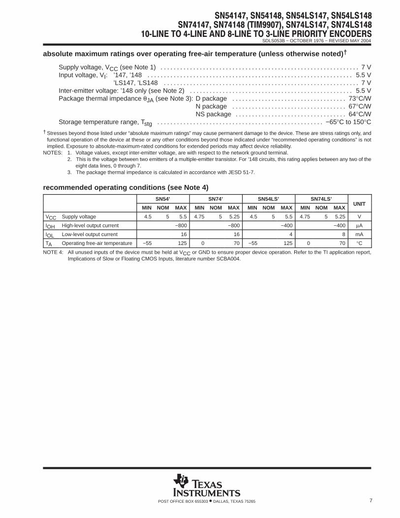
SDLS053B − OCTOBER 1976 − REVISED MAY 2004
7POST OFFICE BOX 655303 • DALLAS, TEXAS 75265
absolute maximum ratings over operating free-air temperature (unless otherwise noted) †
Supply voltage, VCC (see Note 1) 7 V. . . . . . . . . . . . . . . . . . . . . . . . . . . . . . . . . . . . . . . . . . . . . . . . . . . . . . . . . . . . . Input voltage, VI: ’147, ’148 5.5 V. . . . . . . . . . . . . . . . . . . . . . . . . . . . . . . . . . . . . . . . . . . . . . . . . . . . . . . . . . . . . . .
’LS147, ’LS148 7 V. . . . . . . . . . . . . . . . . . . . . . . . . . . . . . . . . . . . . . . . . . . . . . . . . . . . . . . . . . . . Inter-emitter voltage: ’148 only (see Note 2) 5.5 V. . . . . . . . . . . . . . . . . . . . . . . . . . . . . . . . . . . . . . . . . . . . . . . . . . Package thermal impedance θJA (see Note 3): D package 73°C/W. . . . . . . . . . . . . . . . . . . . . . . . . . . . . . . . . . .
N package 67°C/W. . . . . . . . . . . . . . . . . . . . . . . . . . . . . . . . . . . NS package 64°C/W. . . . . . . . . . . . . . . . . . . . . . . . . . . . . . . . . .
Storage temperature range, Tstg −65°C to 150°C. . . . . . . . . . . . . . . . . . . . . . . . . . . . . . . . . . . . . . . . . . . . . . . . . . .
† Stresses beyond those listed under “absolute maximum ratings” may cause permanent damage to the device. These are stress ratings only, andfunctional operation of the device at these or any other conditions beyond those indicated under “recommended operating conditions” is notimplied. Exposure to absolute-maximum-rated conditions for extended periods may affect device reliability.
NOTES: 1. Voltage values, except inter-emitter voltage, are with respect to the network ground terminal.2. This is the voltage between two emitters of a multiple-emitter transistor. For ’148 circuits, this rating applies between any two of the
eight data lines, 0 through 7.3. The package thermal impedance is calculated in accordance with JESD 51-7.
recommended operating conditions (see Note 4)
SN54’ SN74’ SN54LS’ SN74LS’UNIT
MIN NOM MAX MIN NOM MAX MIN NOM MAX MIN NOM MAXUNIT
VCC Supply voltage 4.5 5 5.5 4.75 5 5.25 4.5 5 5.5 4.75 5 5.25 V
IOH High-level output current −800 −800 −400 −400 µA
IOL Low-level output current 16 16 4 8 mA
TA Operating free-air temperature −55 125 0 70 −55 125 0 70 °C
NOTE 4: All unused inputs of the device must be held at VCC or GND to ensure proper device operation. Refer to the TI application report,Implications of Slow or Floating CMOS Inputs, literature number SCBA004.
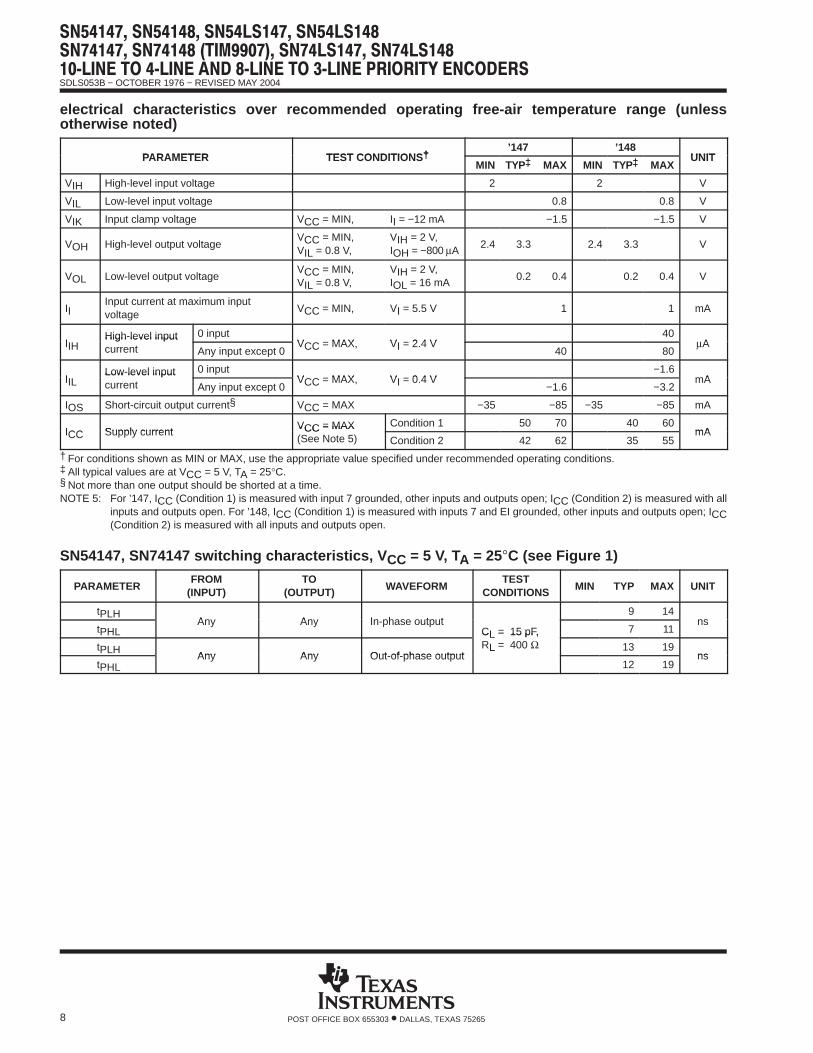
SDLS053B − OCTOBER 1976 − REVISED MAY 2004
8 POST OFFICE BOX 655303 • DALLAS, TEXAS 75265
electrical characteristics over recommended operating free-air temperature range (unlessotherwise noted)
PARAMETER TEST CONDITIONS†’147 ’148
UNITPARAMETER TEST CONDITIONS†MIN TYP‡ MAX MIN TYP‡ MAX
UNIT
VIH High-level input voltage 2 2 V
VIL Low-level input voltage 0.8 0.8 V
VIK Input clamp voltage VCC = MIN, II = −12 mA −1.5 −1.5 V
VOH High-level output voltageVCC = MIN,VIL = 0.8 V,
VIH = 2 V,IOH = −800 µA
2.4 3.3 2.4 3.3 V
VOL Low-level output voltageVCC = MIN,VIL = 0.8 V,
VIH = 2 V,IOL = 16 mA
0.2 0.4 0.2 0.4 V
IIInput current at maximum inputvoltage
VCC = MIN, VI = 5.5 V 1 1 mA
IIHHigh-level input 0 input
VCC = MAX, VI = 2.4 V40
AIIHHigh-level inputcurrent Any input except 0
VCC = MAX, VI = 2.4 V40 80
µA
IILLow-level input 0 input
VCC = MAX, VI = 0.4 V−1.6
mAIILLow-level inputcurrent Any input except 0
VCC = MAX, VI = 0.4 V−1.6 −3.2
mA
IOS Short-circuit output current§ VCC = MAX −35 −85 −35 −85 mA
ICC Supply currentVCC = MAX Condition 1 50 70 40 60
mAICC Supply currentVCC = MAX(See Note 5) Condition 2 42 62 35 55
mA
† For conditions shown as MIN or MAX, use the appropriate value specified under recommended operating conditions.‡ All typical values are at VCC = 5 V, TA = 25°C.§ Not more than one output should be shorted at a time.NOTE 5: For ’147, ICC (Condition 1) is measured with input 7 grounded, other inputs and outputs open; ICC (Condition 2) is measured with all
inputs and outputs open. For ’148, ICC (Condition 1) is measured with inputs 7 and EI grounded, other inputs and outputs open; ICC(Condition 2) is measured with all inputs and outputs open.
SN54147, SN74147 switching characteristics, V CC = 5 V, TA = 25C (see Figure 1)
PARAMETERFROM
(INPUT)TO
(OUTPUT) WAVEFORMTEST
CONDITIONS MIN TYP MAX UNIT
tPLHAny Any In-phase output
9 14ns
tPHLAny Any In-phase output
CL = 15 pF, 7 11ns
tPLHAny Any Out-of-phase output
CL = 15 pF,RL = 400 Ω 13 19
nstPHL
Any Any Out-of-phase outputRL = 400
12 19ns

SDLS053B − OCTOBER 1976 − REVISED MAY 2004
9POST OFFICE BOX 655303 • DALLAS, TEXAS 75265
SN54148, SN74148 switching characteristics, V CC = 5 V, TA = 25C (see Figure 1)
PARAMETER† FROM(INPUT)
TO(OUTPUT) WAVEFORM
TESTCONDITIONS MIN TYP MAX UNIT
tPLH1–7 A0, A1, or A2 In-phase output
10 15ns
tPHL1–7 A0, A1, or A2 In-phase output
9 14ns
tPLH1–7 A0, A1, or A2 Out-of-phase output
13 19ns
tPHL1–7 A0, A1, or A2 Out-of-phase output
12 19ns
tPLH0–7 EO Out-of-phase output
6 10ns
tPHL0–7 EO Out-of-phase output
14 25ns
tPLH0–7 GS In-phase output
CL = 15 pF, 18 30ns
tPHL0–7 GS In-phase output
CL = 15 pF,RL = 400 Ω 14 25
ns
tPLHEI A0, A1, or A2 In-phase output
RL = 400
10 15ns
tPHLEI A0, A1, or A2 In-phase output
10 15ns
tPLHEI GS In-phase output
8 12ns
tPHLEI GS In-phase output
10 15ns
tPLHEI EO In-phase output
10 15ns
tPHLEI EO In-phase output
17 30ns
† tPLH = propagation delay time, low-to-high-level output.tPHL = propagation delay time, high-to-low-level output.
electrical characteristics over recommended operating free-air temperature range (unlessotherwise noted)
PARAMETER TEST CONDITIONS†SN54LS’ SN74LS’
UNITPARAMETER TEST CONDITIONS†MIN TYP‡ MAX MIN TYP‡ MAX
UNIT
VIH High-level input voltage 2 2 V
VIL Low-level input voltage 0.7 0.8 V
VIK Input clamp voltage VCC = MIN, II = −18 mA −1.5 −1.5 V
VOH High-level output voltageVCC = MIN,VIL = 0.8 V,
VIH = 2 V,IOH = −400 µA
2.5 3.4 2.7 3.4 V
VOL Low-level output voltageVCC = MIN,VIH = 2 V,
IOL = 4 mA 0.25 0.4 0.25 0.4VVOL Low-level output voltage
CCVIH = 2 V,VIL = VIL MAX IOL = 8 mA 0.35 0.5
V
II
Input current atmaximum input
’LS148 inputs 1–7VCC = MAX, VI = 7 V
0.2 0.2mAII maximum input
voltage All other inputsVCC = MAX, VI = 7 V
0.1 0.1mA
IIHHigh-level input ’LS148 inputs 1–7
VCC = MAX, VI = 2.7 V40 40
AIIHHigh-level inputcurrent All other inputs
VCC = MAX, VI = 2.7 V20 20
µA
IILLow-level input ’LS148 inputs 1–7
VCC = MAX, VI = 0.4 V−0.8 −0.8
mAIILLow-level inputcurrent All other inputs
VCC = MAX, VI = 0.4 V−0.4 −0.4
mA
IOS Short-circuit output current§ VCC = MAX −20 −100 −20 −100 mA
ICC Supply currentVCC = MAX Condition 1 12 20 12 20
mAICC Supply currentVCC = MAX(See Note 6) Condition 2 10 17 10 17
mA
† For conditions shown as MIN or MAX, use the appropriate value specified under recommended operating conditions.‡ All typical values are at VCC = 5 V, TA = 25°C.§ Not more than one output should be shorted at a time.NOTE 6: For ’LS147, ICC (Condition 1) is measured with input 7 grounded, other inputs and outputs open; ICC (Condition 2) is measured with
all inputs and outputs open. For ’LS148, ICC (Condition 1) is measured with inputs 7 and EI grounded, other inputs and outputs open;ICC (Condition 2) is measured with all inputs and outputs open.

SDLS053B − OCTOBER 1976 − REVISED MAY 2004
10 POST OFFICE BOX 655303 • DALLAS, TEXAS 75265
SN54LS147, SN74LS147 switching characteristics, V CC = 5 V, TA = 25C (see Figure 2)
PARAMETERFROM
(INPUT)TO
(OUTPUT) WAVEFORMTEST
CONDITIONS MIN TYP MAX UNIT
tPLHAny Any In-phase output
12 18ns
tPHLAny Any In-phase output
CL = 15 pF, 12 18ns
tPLHAny Any Out-of-phase output
CL = 15 pF,RL = 2 kΩ 21 33
nstPHL
Any Any Out-of-phase outputRL = 2 k
15 23ns
SN54LS148, SN74LS148 switching characteristics, V CC = 5 V, TA = 25C (see Figure 2)
PARAMETER† FROM(INPUT)
TO(OUTPUT) WAVEFORM
TESTCONDITIONS MIN TYP MAX UNIT
tPLH1–7 A0, A1, or A2 In-phase output
14 18ns
tPHL1–7 A0, A1, or A2 In-phase output
15 25ns
tPLH1–7 A0, A1, or A2 Out-of-phase output
20 36ns
tPHL1–7 A0, A1, or A2 Out-of-phase output
16 29ns
tPLH0–7 EO Out-of-phase output
7 18ns
tPHL0–7 EO Out-of-phase output
25 40ns
tPLH0–7 GS In-phase output
CL = 15 pF, 35 55ns
tPHL0–7 GS In-phase output
CL = 15 pF,RL = 2 kΩ 9 21
ns
tPLHEI A0, A1, or A2 In-phase output
RL = 2 k
16 25ns
tPHLEI A0, A1, or A2 In-phase output
12 25ns
tPLHEI GS In-phase output
12 17ns
tPHLEI GS In-phase output
14 36ns
tPLHEI EO In-phase output
12 21ns
tPHLEI EO In-phase output
23 35ns
† tPLH = propagation delay time, low-to-high-level outputtPHL = propagation delay time, high-to-low-level output

SDLS053B − OCTOBER 1976 − REVISED MAY 2004
11POST OFFICE BOX 655303 • DALLAS, TEXAS 75265
PARAMETER MEASUREMENT INFORMATIONSERIES 54/74 DEVICES
tPHL tPLH
tPLH tPHL
LOAD CIRCUITFOR 3-STATE OUTPUTS
High-LevelPulse
Low-LevelPulse
VOLTAGE WAVEFORMSPULSE DURATIONS
Input
Out-of-PhaseOutput
(see Note D)
3 V
0 V
VOL
VOH
VOH
VOL
In-PhaseOutput
(see Note D)
VOLTAGE WAVEFORMSPROPAGATION DELAY TIMES
VCC
RL
Test Point
From OutputUnder Test
CL(see Note A)
LOAD CIRCUITFOR OPEN-COLLECTOR OUTPUTS
LOAD CIRCUITFOR 2-STATE TOTEM-POLE OUTPUTS
(see Note B)
VCC
RLFrom Output
Under Test
CL(see Note A)
TestPoint
(see Note B )
VCCRL
From OutputUnder Test
CL(see Note A)
TestPoint
1 kΩ
NOTES: A. CL includes probe and jig capacitance.B. All diodes are 1N3064 or equivalent.C. Waveform 1 is for an output with internal conditions such that the output is low, except when disabled by the output control.
Waveform 2 is for an output with internal conditions such that the output is high, except when disabled by the output control.D. S1 and S2 are closed for tPLH, tPHL, tPHZ, and tPLZ; S1 is open, and S2 is closed for tPZH; S1 is closed, and S2 is open for tPZL.E. All input pulses are supplied by generators having the following characteristics: PRR ≤ 1 MHz, ZO ≈ 50 Ω; tr and tf ≤ 7 ns for Series
54/74 devices and tr and tf ≤ 2.5 ns for Series 54S/74S devices.F. The outputs are measured one at a time, with one input transition per measurement.
S1
S2
tPHZ
tPLZtPZL
tPZH
3 V
3 V
0 V
0 V
thtsu
VOLTAGE WAVEFORMSSETUP AND HOLD TIMES
TimingInput
DataInput
3 V
0 V
OutputControl
(low-levelenabling)
Waveform 1(see Notes C
and D)
Waveform 2(see Notes C
and D)≈1.5 V
VOH − 0.5 V
VOL + 0.5 V
≈1.5 V
VOLTAGE WAVEFORMSENABLE AND DISABLE TIMES, 3-STATE OUTPUTS
1.5 V 1.5 V
1.5 V 1.5 V
1.5 V
1.5 V 1.5 V
1.5 V 1.5 V
1.5 V
1.5 V
tw
1.5 V 1.5 V
1.5 V 1.5 V
1.5 V 1.5 V
VOH
VOL
Figure 1. Load Circuits and Voltage Waveforms

SDLS053B − OCTOBER 1976 − REVISED MAY 2004
12 POST OFFICE BOX 655303 • DALLAS, TEXAS 75265
PARAMETER MEASUREMENT INFORMATIONSERIES 54LS/74LS DEVICES
tPHL tPLH
tPLH tPHL
LOAD CIRCUITFOR 3-STATE OUTPUTS
High-LevelPulse
Low-LevelPulse
VOLTAGE WAVEFORMSPULSE DURATIONS
Input
Out-of-PhaseOutput
(see Note D)
3 V
0 V
VOL
VOH
VOH
VOL
In-PhaseOutput
(see Note D)
VOLTAGE WAVEFORMSPROPAGATION DELAY TIMES
VCC
RL
Test Point
From OutputUnder Test
CL(see Note A)
LOAD CIRCUITFOR OPEN-COLLECTOR OUTPUTS
LOAD CIRCUITFOR 2-STATE TOTEM-POLE OUTPUTS
(see Note B)
VCC
RLFrom Output
Under Test
CL(see Note A)
TestPoint
(see Note B )
VCCRL
From OutputUnder Test
CL(see Note A)
TestPoint
5 kΩ
NOTES: A. CL includes probe and jig capacitance.B. All diodes are 1N3064 or equivalent.C. Waveform 1 is for an output with internal conditions such that the output is low, except when disabled by the output control.
Waveform 2 is for an output with internal conditions such that the output is high, except when disabled by the output control.D. S1 and S2 are closed for tPLH, tPHL, tPHZ, and tPLZ; S1 is open, and S2 is closed for tPZH; S1 is closed, and S2 is open for tPZL.E. Phase relationships between inputs and outputs have been chosen arbitrarily for these examples.F. All input pulses are supplied by generators having the following characteristics: PRR ≤ 1 MHz, ZO ≈ 50 Ω, tr ≤ 1.5 ns, tf ≤ 2.6 ns.G. The outputs are measured one at a time, with one input transition per measurement.
S1
S2
tPHZ
tPLZtPZL
tPZH
3 V
3 V
0 V
0 V
thtsu
VOLTAGE WAVEFORMSSETUP AND HOLD TIMES
TimingInput
DataInput
3 V
0 V
OutputControl
(low-levelenabling)
Waveform 1(see Notes C
and D)
Waveform 2(see Notes C
and D) ≈1.5 V
VOH − 0.5 V
VOL + 0.5 V
≈1.5 V
VOLTAGE WAVEFORMSENABLE AND DISABLE TIMES, 3-STATE OUTPUTS
1.3 V 1.3 V
1.3 V 1.3 V
1.3 V
1.3 V 1.3 V
1.3 V 1.3 V
1.3 V
1.3 V
tw
1.3 V 1.3 V
1.3 V 1.3 V
1.3 V 1.3 V
VOL
VOH
Figure 2. Load Circuits and Voltage Waveforms

SDLS053B − OCTOBER 1976 − REVISED MAY 2004
13POST OFFICE BOX 655303 • DALLAS, TEXAS 75265
APPLICATION INFORMATION
0 1 2 3 4 5 6 7 EI
EO A0 A1 A2 GS
’148/’LS148
0 1 2 3 4 5 6 7 EI
EO A0 A1 A2 GS
’148/LS148
’08/’LS08
0 1 2 3 4 5 6 7 9 10 11 12 13 14 15 Enable(active low)
0 1 2 3
Encoded Data (active low)
Priority Flag(active low)
16-Line Data (active low)
0 1 2 3 4 5 6 7 EI
EO A0 A1 A2 GS
’148/’LS148
0 1 2 3 4 5 6 7 EI
EO A0 A1 A2 GS
’148/’LS148
’HC00
0 1 2 3 4 5 6 7 8 9 10 11 12 13 14 15 Enable(active low)
0 1 2 3
Encoded Data (active high)
Priority Flag(active high)
16-Line Data (active low)
8
Figure 3. Priority Encoder for 16 Bits
Because the ’147/’LS147 and ’148/’LS148 devices are combinational logic circuits, wrong addresses can appearduring input transients. Moreover, for the ’148/’LS148 devices, a change from high to low at EI can cause a transientlow on GS when all inputs are high. This must be considered when strobing the outputs.

PACKAGING INFORMATION
Orderable Device Status (1) PackageType
PackageDrawing
Pins PackageQty
Eco Plan (2) Lead/Ball Finish MSL Peak Temp (3)
78027012A ACTIVE LCCC FK 20 1 TBD Call TI Level-NC-NC-NC
7802701EA ACTIVE CDIP J 16 1 TBD Call TI Level-NC-NC-NC
7802701FA ACTIVE CFP W 16 1 TBD Call TI Level-NC-NC-NC
JM38510/36001B2A ACTIVE LCCC FK 20 1 TBD Call TI Level-NC-NC-NC
JM38510/36001BEA ACTIVE CDIP J 16 1 TBD Call TI Level-NC-NC-NC
JM38510/36001BFA ACTIVE CFP W 16 1 TBD Call TI Level-NC-NC-NC
SN54148J OBSOLETE CDIP J 16 TBD Call TI Call TI
SN54LS148J ACTIVE CDIP J 16 1 TBD Call TI Level-NC-NC-NC
SN74147N OBSOLETE PDIP N 16 TBD Call TI Call TI
SN74148J OBSOLETE CDIP J 16 TBD Call TI Call TI
SN74148N OBSOLETE PDIP N 16 TBD Call TI Call TI
SN74148N3 OBSOLETE PDIP N 16 TBD Call TI Call TI
SN74LS147DR OBSOLETE SOIC D 16 TBD Call TI Call TI
SN74LS147N OBSOLETE PDIP N 16 TBD Call TI Call TI
SN74LS148D ACTIVE SOIC D 16 40 Green (RoHS &no Sb/Br)
CU NIPDAU Level-1-260C-UNLIM
SN74LS148DE4 ACTIVE SOIC D 16 40 Green (RoHS &no Sb/Br)
CU NIPDAU Level-1-260C-UNLIM
SN74LS148DR ACTIVE SOIC D 16 2500 Green (RoHS &no Sb/Br)
CU NIPDAU Level-1-260C-UNLIM
SN74LS148DRE4 ACTIVE SOIC D 16 2500 Green (RoHS &no Sb/Br)
CU NIPDAU Level-1-260C-UNLIM
SN74LS148J OBSOLETE CDIP J 16 TBD Call TI Call TI
SN74LS148N ACTIVE PDIP N 16 25 Pb-Free(RoHS)
CU NIPDAU Level-NC-NC-NC
SN74LS148N3 OBSOLETE PDIP N 16 TBD Call TI Call TI
SN74LS148NE4 ACTIVE PDIP N 16 25 Pb-Free(RoHS)
CU NIPDAU Level-NC-NC-NC
SN74LS148NSR ACTIVE SO NS 16 2000 Green (RoHS &no Sb/Br)
CU NIPDAU Level-1-260C-UNLIM
SN74LS148NSRE4 ACTIVE SO NS 16 2000 Green (RoHS &no Sb/Br)
CU NIPDAU Level-1-260C-UNLIM
SNJ54148J OBSOLETE CDIP J 16 TBD Call TI Call TI
SNJ54148W OBSOLETE CFP W 16 TBD Call TI Call TI
SNJ54LS148FK ACTIVE LCCC FK 20 1 TBD Call TI Level-NC-NC-NC
SNJ54LS148J ACTIVE CDIP J 16 1 TBD Call TI Level-NC-NC-NC
SNJ54LS148W ACTIVE CFP W 16 1 TBD Call TI Level-NC-NC-NC
(1) The marketing status values are defined as follows:ACTIVE: Product device recommended for new designs.LIFEBUY: TI has announced that the device will be discontinued, and a lifetime-buy period is in effect.NRND: Not recommended for new designs. Device is in production to support existing customers, but TI does not recommend using this part ina new design.PREVIEW: Device has been announced but is not in production. Samples may or may not be available.OBSOLETE: TI has discontinued the production of the device.
(2) Eco Plan - The planned eco-friendly classification: Pb-Free (RoHS) or Green (RoHS & no Sb/Br) - please check
PACKAGE OPTION ADDENDUM
www.ti.com 26-Sep-2005
Addendum-Page 1

http://www.ti.com/productcontent for the latest availability information and additional product content details.TBD: The Pb-Free/Green conversion plan has not been defined.Pb-Free (RoHS): TI's terms "Lead-Free" or "Pb-Free" mean semiconductor products that are compatible with the current RoHS requirementsfor all 6 substances, including the requirement that lead not exceed 0.1% by weight in homogeneous materials. Where designed to be solderedat high temperatures, TI Pb-Free products are suitable for use in specified lead-free processes.Green (RoHS & no Sb/Br): TI defines "Green" to mean Pb-Free (RoHS compatible), and free of Bromine (Br) and Antimony (Sb) based flameretardants (Br or Sb do not exceed 0.1% by weight in homogeneous material)
(3) MSL, Peak Temp. -- The Moisture Sensitivity Level rating according to the JEDEC industry standard classifications, and peak soldertemperature.
Important Information and Disclaimer:The information provided on this page represents TI's knowledge and belief as of the date that it isprovided. TI bases its knowledge and belief on information provided by third parties, and makes no representation or warranty as to theaccuracy of such information. Efforts are underway to better integrate information from third parties. TI has taken and continues to takereasonable steps to provide representative and accurate information but may not have conducted destructive testing or chemical analysis onincoming materials and chemicals. TI and TI suppliers consider certain information to be proprietary, and thus CAS numbers and other limitedinformation may not be available for release.
In no event shall TI's liability arising out of such information exceed the total purchase price of the TI part(s) at issue in this document sold by TIto Customer on an annual basis.
PACKAGE OPTION ADDENDUM
www.ti.com 26-Sep-2005
Addendum-Page 2


MECHANICAL DATA
MLCC006B – OCTOBER 1996
POST OFFICE BOX 655303 • DALLAS, TEXAS 75265
FK (S-CQCC-N**) LEADLESS CERAMIC CHIP CARRIER
4040140/D 10/96
28 TERMINAL SHOWN
B
0.358(9,09)
MAX
(11,63)
0.560(14,22)
0.560
0.458
0.858(21,8)
1.063(27,0)
(14,22)
ANO. OF
MINMAX
0.358
0.660
0.761
0.458
0.342(8,69)
MIN
(11,23)
(16,26)0.640
0.739
0.442
(9,09)
(11,63)
(16,76)
0.962
1.165
(23,83)0.938
(28,99)1.141
(24,43)
(29,59)
(19,32)(18,78)
**
20
28
52
44
68
84
0.020 (0,51)
TERMINALS
0.080 (2,03)0.064 (1,63)
(7,80)0.307
(10,31)0.406
(12,58)0.495
(12,58)0.495
(21,6)0.850
(26,6)1.047
0.045 (1,14)
0.045 (1,14)0.035 (0,89)
0.035 (0,89)
0.010 (0,25)
121314151618 17
11
10
8
9
7
5
432
0.020 (0,51)0.010 (0,25)
6
12826 27
19
21B SQ
A SQ22
23
24
25
20
0.055 (1,40)0.045 (1,14)
0.028 (0,71)0.022 (0,54)
0.050 (1,27)
NOTES: A. All linear dimensions are in inches (millimeters).B. This drawing is subject to change without notice.C. This package can be hermetically sealed with a metal lid.D. The terminals are gold plated.E. Falls within JEDEC MS-004


IMPORTANT NOTICE
Texas Instruments Incorporated and its subsidiaries (TI) reserve the right to make corrections, modifications,enhancements, improvements, and other changes to its products and services at any time and to discontinueany product or service without notice. Customers should obtain the latest relevant information before placingorders and should verify that such information is current and complete. All products are sold subject to TI’s termsand conditions of sale supplied at the time of order acknowledgment.
TI warrants performance of its hardware products to the specifications applicable at the time of sale inaccordance with TI’s standard warranty. Testing and other quality control techniques are used to the extent TIdeems necessary to support this warranty. Except where mandated by government requirements, testing of allparameters of each product is not necessarily performed.
TI assumes no liability for applications assistance or customer product design. Customers are responsible fortheir products and applications using TI components. To minimize the risks associated with customer productsand applications, customers should provide adequate design and operating safeguards.
TI does not warrant or represent that any license, either express or implied, is granted under any TI patent right,copyright, mask work right, or other TI intellectual property right relating to any combination, machine, or processin which TI products or services are used. Information published by TI regarding third-party products or servicesdoes not constitute a license from TI to use such products or services or a warranty or endorsement thereof.Use of such information may require a license from a third party under the patents or other intellectual propertyof the third party, or a license from TI under the patents or other intellectual property of TI.
Reproduction of information in TI data books or data sheets is permissible only if reproduction is withoutalteration and is accompanied by all associated warranties, conditions, limitations, and notices. Reproductionof this information with alteration is an unfair and deceptive business practice. TI is not responsible or liable forsuch altered documentation.
Resale of TI products or services with statements different from or beyond the parameters stated by TI for thatproduct or service voids all express and any implied warranties for the associated TI product or service andis an unfair and deceptive business practice. TI is not responsible or liable for any such statements.
Following are URLs where you can obtain information on other Texas Instruments products and applicationsolutions:
Products Applications
Amplifiers amplifier.ti.com Audio www.ti.com/audio
Data Converters dataconverter.ti.com Automotive www.ti.com/automotive
DSP dsp.ti.com Broadband www.ti.com/broadband
Interface interface.ti.com Digital Control www.ti.com/digitalcontrol
Logic logic.ti.com Military www.ti.com/military
Power Mgmt power.ti.com Optical Networking www.ti.com/opticalnetwork
Microcontrollers microcontroller.ti.com Security www.ti.com/security
Telephony www.ti.com/telephony
Video & Imaging www.ti.com/video
Wireless www.ti.com/wireless
Mailing Address: Texas Instruments
Post Office Box 655303 Dallas, Texas 75265
Copyright 2005, Texas Instruments Incorporated

TL/F/6546
54150/D
M54150/D
M74150,54151A
/D
M54151A
/D
M74151A
Data
Sele
cto
rs/M
ultip
lexers
June 1989
54150/DM54150/DM74150,54151A/DM54151A/DM74151AData Selectors/Multiplexers
General DescriptionThese data selectors/multiplexers contain full on-chip de-
coding to select the desired data source. The 150 selects
one-of-sixteen data sources; the 151A selects one-of-eight
data sources. The 150 and 151A have a strobe input which
must be at a low logic level to enable these devices. A high
level at the strobe forces the W output high and the Y output
(as applicable) low.
The 151A features complementary W and Y outputs, where-
as the 150 has an inverted (W) output only.
The 151A incorporates address buffers which have sym-
metrical propagation delay times through the complementa-
ry paths. This reduces the possibility of transients occurring
at the output(s) due to changes made at the select inputs,
even when the 151A outputs are enabled (i.e., strobe low).
FeaturesY 150 selects one-of-sixteen data linesY 151A selects one-of-eight data linesY Performs parallel-to-serial conversionY Permits multiplexing from N lines to one lineY Also for use as Boolean function generatorY Typical average propagation delay time, data input to W
output
150 11 ns
151A 9 nsY Typical power dissipation
150 200 mW
151A 135 mWY Alternate Military/Aerospace device (54150, 54151A) is
available. Contact a National Semiconductor Sales Of-
fice/Distributor for specifications.
Connection Diagrams
Dual-In-Line Package
TL/F/6546–1
Order Number 54150DQMB, 54150FMQB,
DM54150J or DM74150N
See NS Package Number J24A, N24A or W24C
Dual-In-Line Package
TL/F/6546–2
Order Number 54151ADMQB, 54151AFMQB,
DM54151AJ, DM54151AW or DM74151AN
See NS Package Number J16A, N16E or W16A
C1995 National Semiconductor Corporation RRD-B30M105/Printed in U. S. A.

Absolute Maximum Ratings (Note)
If Military/Aerospace specified devices are required,
please contact the National Semiconductor Sales
Office/Distributors for availability and specifications.
Supply Voltage 7V
Input Voltage 5.5V
Operating Free Air Temperature Range
DM54 and 54 b55§C to a125§CDM74 0§C to a70§C
Storage Temperature Range b65§C to a150§C
Note: The ‘‘Absolute Maximum Ratings’’ are those valuesbeyond which the safety of the device cannot be guaran-teed. The device should not be operated at these limits. Theparametric values defined in the ‘‘Electrical Characteristics’’table are not guaranteed at the absolute maximum ratings.The ‘‘Recommended Operating Conditions’’ table will definethe conditions for actual device operation.
Recommended Operating Conditions
Symbol ParameterDM54150 DM74150
UnitsMin Nom Max Min Nom Max
VCC Supply Voltage 4.5 5 5.5 4.75 5 5.25 V
VIH High Level Input Voltage 2 2 V
VIL Low Level Input Voltage 0.8 0.8 V
IOH High Level Output Current b0.8 b0.8 mA
IOL Low Level Output Current 16 16 mA
TA Free Air Operating Temperature b55 125 0 70 §C
’150 Electrical Characteristicsover recommended operating free air temperature range (unless otherwise noted)
Symbol Parameter Conditions MinTyp
Max Units(Note 1)
VI Input Clamp Voltage VCC e Min, II e b12 mA b1.5 V
VOH High Level Output VCC e Min, IOH e Max2.4 V
Voltage VIL e Max, VIH e Min
VOL Low Level Output VCC e Min, IOL e Max0.4 V
Voltage VIH e Min, VIL e Max
II Input Current @ Max VCC e Max, VI e 5.5V1 mA
Input Voltage
IIH High Level Input Current VCC e Max, VI e 2.4V 40 mA
IIL Low Level Input Current VCC e Max, VI e 0.4V b1.6 mA
IOS Short Circuit VCC e Max DM54 b20 b55mA
Output Current (Note 2)DM74 b18 b55
ICC Supply Current VCC e Max, (Note 3) 40 68 mA
Note 1: All typicals are at VCC e 5V, TA e 25§C.
Note 2: Not more than one output should be shorted at a time.
Note 3: ICC is measured with the strobe and data select inputs at 4.5V, all other inputs and outputs open.
2

’150 Switching Characteristicsat VCC e 5V and TA e 25§C (See Section 1 for Test Waveforms and Output Load)
Symbol ParameterFrom (Input) RL e 400X, CL e 15 pF
UnitsTo (Output) Min Max
tPLH Propagation Delay Time Select35 ns
Low to High Level Output to W
tPHL Propagation Delay Time Select33 ns
High to Low Level Output to W
tPLH Propagation Delay Time Strobe24 ns
Low to High Level Output to W
tPHL Propagation Delay Time Strobe30 ns
High to Low Level Output to W
tPLH Propagation Delay Time E0-E1520 ns
Low to High Level Output to W
tPHL Propagation Delay Time E0-E1514 ns
High to Low Level Output to W
Recommended Operating Conditions
Symbol ParameterDM54151A DM74151A
UnitsMin Nom Max Min Nom Max
VCC Supply Voltage 4.5 5 5.5 4.75 5 5.25 V
VIH High Level Input Voltage 2 2 V
VIL Low Level Input Voltage 0.8 0.8 V
IOH High Level Output Current b0.8 b0.8 mA
IOL Low Level Output Current 16 16 mA
TA Free Air Operating Temperature b55 125 0 70 §C
3

’151A Electrical Characteristicsover recommended operating free air temperature range (unless otherwise noted)
Symbol Parameter Conditions MinTyp
Max Units(Note 1)
VI Input Clamp Voltage VCC e Min, II e b12 mA b1.5 V
VOH High Level Output VCC e Min, IOH e Max2.4 V
Voltage VIL e Max, VIH e Min
VOL Low Level Output VCC e Min, IOL e Max0.4 V
Voltage VIH e Min, VIL e Max
II Input Current @ Max VCC e Max, VI e 5.5V1 mA
Input Voltage
IIH High Level Input Current VCC e Max, VI e 2.4V 40 mA
IIL Low Level Input Current VCC e Max, VI e 0.4V b1.6 mA
IOS Short Circuit VCC e Max DM54 b20 b55mA
Output Current (Note 2)DM74 b18 b55
ICC Supply Current VCC e Max, (Note 3) 27 48 mA
Note 1: All typicals are at VCC e 5V, TA e 25§C.
Note 2: Not more than one output should be shorted at a time.
Note 3: ICC is measured with the strobe and data select inputs at 4.5V, all other inputs and outputs open.
’151A Switching Characteristicsat VCC e 5V and TA e 25§C (See Section 1 for Test Waveforms and Output Load)
Symbol Parameter From (Input) RL e 400X, CL e 15 pFUnits
To (Output) Min Max
tPLH Propagation Delay Time Select38 ns
Low to High Level Output (4 Levels) to Y
tPHL Propagation Delay Time Select30 ns
High to Low Level Output (4 Levels) to Y
tPLH Propagation Delay Time Select26 ns
Low to High Level Output (3 Levels) to W
tPHL Propagation Delay Time Select30 ns
High to Low Level Output (3 Levels) to W
tPLH Propagation Delay Time Strobe33 ns
Low to High Level Output to Y
tPHL Propagation Delay Time Strobe30 ns
High to Low Level Output to Y
tPLH Propagation Delay Time Strobe21 ns
Low to High Level Output to W
tPHL Propagation Delay Time Strobe25 ns
High to Low Level Output to W
tPLH Propagation Delay Time D0-D724 ns
Low to High Level Output to Y
tPHL Propagation Delay Time D0-D724 ns
High to Low Level Output to Y
tPLH Propagation Delay Time D0-D714 ns
Low to High Level Output to W
tPHL Propagation Delay Time D0-D714 ns
High to Low Level Output to W
4

Logic Diagrams150
TL/F/6546–3
5

Logic Diagrams151A
TL/F/6546–4
See Address Buffers Below
Address Buffers for
54151A/74151A
TL/F/6546–5
Function Tables54150/74150
Inputs
OutputsSelect Strobe
W
D C B AS
X X X X H H
L L L L L E0
L L L H L E1
L L H L L E2
L L H H L E3
L H L L L E4
L H L H L E5
L H H L L E6
L H H H L E7
H L L L L E8
H L L H L E9
H L H L L E10
H L H H L E11
H H L L L E12
H H L H L E13
H H H L L E14
H H H H L E15
H e High Level, L e Low Level, X e Don’t Care
E0, E1 . . . E15 e the complement of the level of the respective E input
54151A/75151A
Inputs Outputs
Select StrobeY W
C B AS
X X X H L H
L L L L D0 D0
L L H L D1 D1
L H L L D2 D2
L H H L D3 D3
H L L L D4 D4
H L H L D5 D5
H H L L D6 D6
H H H L D7 D7
H e High Level, L e Low Level, X e Don’t Care
D0, D1 . . . D7 e the level of the respective D input
6

Physical Dimensions inches (millimeters)
16-Lead Ceramic Dual-In-Line Package (J)
Order Number 54151ADMQB or DM54151AJ
NS Package Number J16A
24-Lead Ceramic Dual-In-Line Package (J)
Order Number 54150DMQB or DM54150J
NS Package Number J24A
7

Physical Dimensions inches (millimeters) (Continued)
16-Lead Molded Dual-In-Line Package (N)
Order Number DM74151AN
NS Package Number N16E
24-Lead Molded Dual-In-Line Package (N)
Order Number DM74150N
NS Package Number N24A
8

Physical Dimensions inches (millimeters) (Continued)
16-Lead Ceramic Flat Package (W)
Order Number 54151AFMQB or DM54151AW
NS Package Number W16A
9

54150/D
M54150/D
M74150,54151A
/D
M54151A
/D
M74151A
Data
Sele
cto
rs/M
ultip
lexers
Physical Dimensions inches (millimeters) (Continued)
24-Lead Ceramic Flat Package (W)
Order Number 54150FMQB
NS Package Number W24C
LIFE SUPPORT POLICY
NATIONAL’S PRODUCTS ARE NOT AUTHORIZED FOR USE AS CRITICAL COMPONENTS IN LIFE SUPPORT
DEVICES OR SYSTEMS WITHOUT THE EXPRESS WRITTEN APPROVAL OF THE PRESIDENT OF NATIONAL
SEMICONDUCTOR CORPORATION. As used herein:
1. Life support devices or systems are devices or 2. A critical component is any component of a life
systems which, (a) are intended for surgical implant support device or system whose failure to perform can
into the body, or (b) support or sustain life, and whose be reasonably expected to cause the failure of the life
failure to perform, when properly used in accordance support device or system, or to affect its safety or
with instructions for use provided in the labeling, can effectiveness.
be reasonably expected to result in a significant injury
to the user.
National Semiconductor National Semiconductor National Semiconductor National SemiconductorCorporation Europe Hong Kong Ltd. Japan Ltd.1111 West Bardin Road Fax: (a49) 0-180-530 85 86 13th Floor, Straight Block, Tel: 81-043-299-2309Arlington, TX 76017 Email: cnjwge@ tevm2.nsc.com Ocean Centre, 5 Canton Rd. Fax: 81-043-299-2408Tel: 1(800) 272-9959 Deutsch Tel: (a49) 0-180-530 85 85 Tsimshatsui, KowloonFax: 1(800) 737-7018 English Tel: (a49) 0-180-532 78 32 Hong Kong
Fran3ais Tel: (a49) 0-180-532 93 58 Tel: (852) 2737-1600Italiano Tel: (a49) 0-180-534 16 80 Fax: (852) 2736-9960
National does not assume any responsibility for use of any circuitry described, no circuit patent licenses are implied and National reserves the right at any time without notice to change said circuitry and specifications.

SN54190, SN54191, SN54LS190, SN54LS191,SN74190, SN74191, SN74LS190, SN74LS191
SYNCHRONOUS UP/DOWN COUNTERS WITH DOWN/UP MODE CONTROL
SDLS072 – DECEMBER 1972 – REVISED MARCH 1988
1POST OFFICE BOX 655303 • DALLAS, TEXAS 75265
Copyright 1988, Texas Instruments IncorporatedPRODUCTION DATA information is current as of publication date.Products conform to specifications per the terms of Texas Instrumentsstandard warranty. Production processing does not necessarily includetesting of all parameters.

SN54190, SN54191, SN54LS190, SN54LS191,SN74190, SN74191, SN74LS190, SN74LS191SYNCHRONOUS UP/DOWN COUNTERS WITH DOWN/UP MODE CONTROL
SDLS072 – DECEMBER 1972 – REVISED MARCH 1988
2 POST OFFICE BOX 655303 • DALLAS, TEXAS 75265

SN54190, SN54LS190, SN74190, SN74LS190SYNCHRONOUS UP/DOWN COUNTERS WITH DOWN/UP MODE CONTROL
SDLS072 – DECEMBER 1972 – REVISED MARCH 1988
3POST OFFICE BOX 655303 • DALLAS, TEXAS 75265
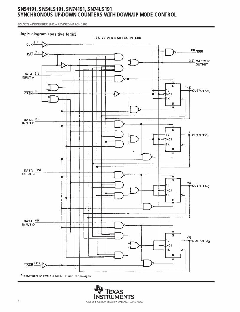
SN54191, SN54LS191, SN74191, SN74LS191SYNCHRONOUS UP/DOWN COUNTERS WITH DOWN/UP MODE CONTROL
SDLS072 – DECEMBER 1972 – REVISED MARCH 1988
4 POST OFFICE BOX 655303 • DALLAS, TEXAS 75265

SN54190, SN54LS190, SN74190, SN74LS190SYNCHRONOUS UP/DOWN COUNTERS WITH DOWN/UP MODE CONTROL
SDLS072 – DECEMBER 1972 – REVISED MARCH 1988
5POST OFFICE BOX 655303 • DALLAS, TEXAS 75265
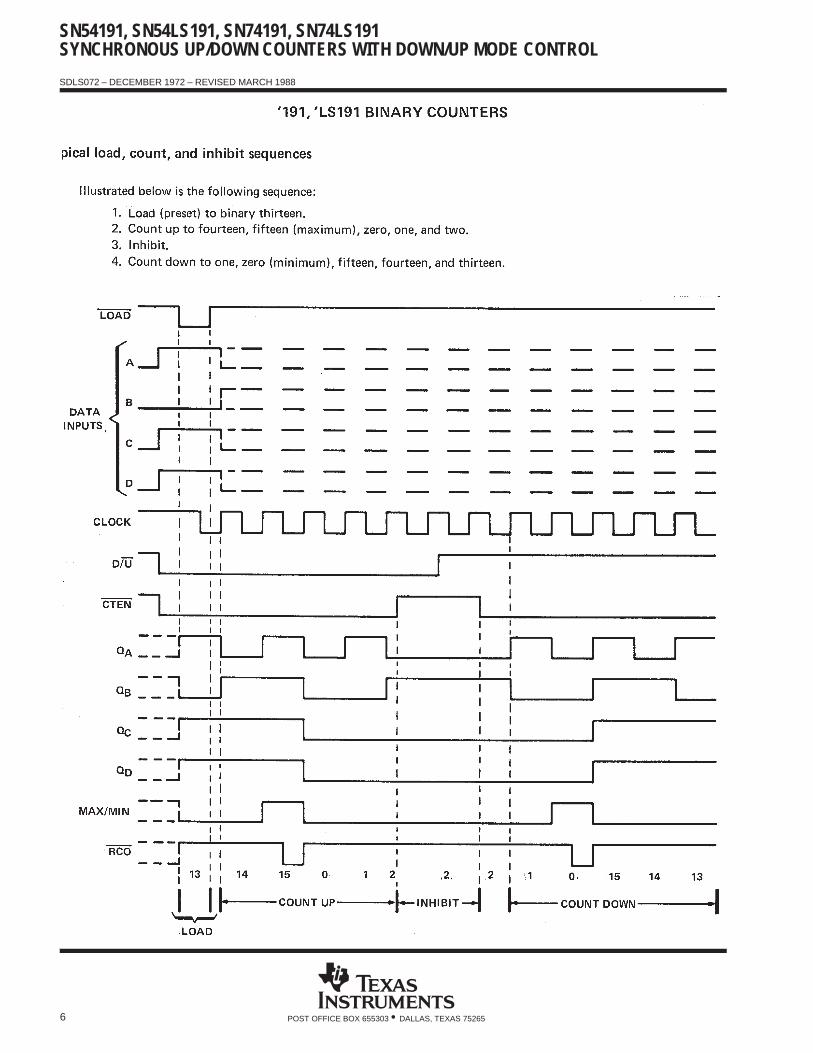
SN54191, SN54LS191, SN74191, SN74LS191SYNCHRONOUS UP/DOWN COUNTERS WITH DOWN/UP MODE CONTROL
SDLS072 – DECEMBER 1972 – REVISED MARCH 1988
6 POST OFFICE BOX 655303 • DALLAS, TEXAS 75265

SN54190, SN54191, SN54LS190, SN54LS191,SN74190, SN74191, SN74LS190, SN74LS191
SYNCHRONOUS UP/DOWN COUNTERS WITH DOWN/UP MODE CONTROL
SDLS072 – DECEMBER 1972 – REVISED MARCH 1988
7POST OFFICE BOX 655303 • DALLAS, TEXAS 75265

SN54190, SN54191, SN74190, SN74191SYNCHRONOUS UP/DOWN COUNTERS WITH DOWN/UP MODE CONTROL
SDLS072 – DECEMBER 1972 – REVISED MARCH 1988
8 POST OFFICE BOX 655303 • DALLAS, TEXAS 75265

SN54LS190, SN54LS191, SN74LS190, SN74LS191SYNCHRONOUS UP/DOWN COUNTERS WITH DOWN/UP MODE CONTROL
SDLS072 – DECEMBER 1972 – REVISED MARCH 1988
9POST OFFICE BOX 655303 • DALLAS, TEXAS 75265

SN54LS190, SN54LS191, SN74LS190, SN74LS191SYNCHRONOUS UP/DOWN COUNTERS WITH DOWN/UP MODE CONTROL
SDLS072 – DECEMBER 1972 – REVISED MARCH 1988
10 POST OFFICE BOX 655303 • DALLAS, TEXAS 75265

SN54190, SN54191, SN54LS190, SN54LS191,SN74190, SN74191, SN74LS190, SN74LS191
SYNCHRONOUS UP/DOWN COUNTERS WITH DOWN/UP MODE CONTROL
SDLS072 – DECEMBER 1972 – REVISED MARCH 1988
11POST OFFICE BOX 655303 • DALLAS, TEXAS 75265

SN54190, SN54191, SN54LS190, SN54LS191,SN74190, SN74191, SN74LS190, SN74LS191SYNCHRONOUS UP/DOWN COUNTERS WITH DOWN/UP MODE CONTROL
SDLS072 – DECEMBER 1972 – REVISED MARCH 1988
12 POST OFFICE BOX 655303 • DALLAS, TEXAS 75265

SN54190, SN54191, SN54LS190, SN54LS191,SN74190, SN74191, SN74LS190, SN74LS191
SYNCHRONOUS UP/DOWN COUNTERS WITH DOWN/UP MODE CONTROL
SDLS072 – DECEMBER 1972 – REVISED MARCH 1988
13POST OFFICE BOX 655303 • DALLAS, TEXAS 75265

IMPORTANT NOTICE
Texas Instruments and its subsidiaries (TI) reserve the right to make changes to their products or to discontinueany product or service without notice, and advise customers to obtain the latest version of relevant informationto verify, before placing orders, that information being relied on is current and complete. All products are soldsubject to the terms and conditions of sale supplied at the time of order acknowledgement, including thosepertaining to warranty, patent infringement, and limitation of liability.
TI warrants performance of its semiconductor products to the specifications applicable at the time of sale inaccordance with TI’s standard warranty. Testing and other quality control techniques are utilized to the extentTI deems necessary to support this warranty. Specific testing of all parameters of each device is not necessarilyperformed, except those mandated by government requirements.
CERTAIN APPLICATIONS USING SEMICONDUCTOR PRODUCTS MAY INVOLVE POTENTIAL RISKS OFDEATH, PERSONAL INJURY, OR SEVERE PROPERTY OR ENVIRONMENTAL DAMAGE (“CRITICALAPPLICATIONS”). TI SEMICONDUCTOR PRODUCTS ARE NOT DESIGNED, AUTHORIZED, ORWARRANTED TO BE SUITABLE FOR USE IN LIFE-SUPPORT DEVICES OR SYSTEMS OR OTHERCRITICAL APPLICATIONS. INCLUSION OF TI PRODUCTS IN SUCH APPLICATIONS IS UNDERSTOOD TOBE FULLY AT THE CUSTOMER’S RISK.
In order to minimize risks associated with the customer’s applications, adequate design and operatingsafeguards must be provided by the customer to minimize inherent or procedural hazards.
TI assumes no liability for applications assistance or customer product design. TI does not warrant or representthat any license, either express or implied, is granted under any patent right, copyright, mask work right, or otherintellectual property right of TI covering or relating to any combination, machine, or process in which suchsemiconductor products or services might be or are used. TI’s publication of information regarding any thirdparty’s products or services does not constitute TI’s approval, warranty or endorsement thereof.
Copyright 1999, Texas Instruments Incorporated

© 2000 Fairchild Semiconductor Corporation DS010182 www.fairchildsemi.com
March 1989
Revised March 2000
DM
74LS
266 Qu
ad 2-In
pu
t Exclu
sive-NO
R G
ate
DM74LS266Quad 2-Input Exclusive-NOR Gate with Open-Collector Outputs
General DescriptionThis device contains four independent gates each of whichperforms the logic exclusive-NOR function. Outputs areopen collector.
Ordering Code:
Devices also available in Tape and Reel. Specify by appending the suffix letter “X” to the ordering code.
Connection Diagram Truth Table
H = HIGH Voltage LevelL = LOW Voltage Level
Order Number Package Number Package Description
DM74LS266M M14A 14-Lead Small Outline Integrated Circuit (SOIC), JEDEC MS-120, 0.150 Narrow
DM74LS266N N14A 14-Lead Plastic Dual-In-Line Package (PDIP), JEDEC MS-001, 0.300 Wide
Inputs Outputs
A B Y
L L H
L H L
H L L
H H H

www.fairchildsemi.com 2
DM
74L
S26
6Absolute Maximum Ratings(Note 1)
Note 1: The “Absolute Maximum Ratings” are those values beyond whichthe safety of the device cannot be guaranteed. The device should not beoperated at these limits. The parametric values defined in the “ElectricalCharacteristics” table are not guaranteed at the absolute maximum ratings.The “Recommended Operating Conditions” table will define the conditionsfor actual device operation.
Recommended Operating Conditions
Electrical Characteristics over recommended operating free air temperature range (unless otherwise noted)
Note 2: All typicals are at VCC = 5V, TA = 25°C.
Note 3: Not more than one output should be shorted at a time, and the duration should not exceed one second.
Switching Characteristics VCC = 5V, TA = 25°C
Supply Voltage 7V
Input Voltage 7V
Operating Free Air Temperature Range 0°C to +70°C
Storage Temperature Range −65°C to +150°C
Symbol Parameter Min Nom Max Units
VCC Supply Voltage 4.75 5 5.25 V
VIH HIGH Level Input Voltage 2 V
VIL LOW Level Input Voltage 0.8 V
VOH HIGH Level Output Voltage 5.5 V
IOL LOW Level Output Current 8 mA
TA Free Air Operating Temperature 0 70 °C
Symbol Parameter Conditions MinTyp
Max Units(Note 2)
VI Input Clamp Voltage VCC = Min, II = −18 mA −1.5 V
ICEX HIGH Level VCC = Min, VO = 5.5V,100 µA
Output Current VIL = Max
VOL LOW Level VCC = Min, IOL = Max,0.5
Output Voltage VIH = Min V
IOL = 4 mA, VCC = Min 0.4
II Input Current @ Max Input Voltage VCC = Max, VI = 7V 0.2 mA
IIH HIGH Level Input Current VCC = Max, VI = 2.7V 40 µA
IIL LOW Level Input Current VCC = Max, VI = 0.4V −0.8 mA
IOS Short Circuit Output Current VCC = Max (Note 3) −20 −100 mA
ICC Supply Current VCC = Max 13 mA
RL = 2 kΩ
Symbol Parameter CL = 15 pF Units
Min Max
tPLH Propagation Delay Time23 ns
LOW-to-HIGH Level Output
tPHL Propagation Delay Time23 ns
HIGH-to-LOW Level Output

3 www.fairchildsemi.com
DM
74LS
266Physical Dimensions inches (millimeters) unless otherwise noted
14-Lead Small Outline Integrated Circuit (SOIC), JEDEC MS-120, 0.150 NarrowPackage Number M14A

www.fairchildsemi.com 4
DM
74L
S26
6 Q
uad
2-I
np
ut
Exc
lusi
ve-N
OR
Gat
ePhysical Dimensions inches (millimeters) unless otherwise noted (Continued)
14-Lead Plastic Dual-In-Line Package (PDIP), JEDEC MS-001, 0.300 WidePackage Number N14A
Fairchild does not assume any responsibility for use of any circuitry described, no circuit patent licenses are implied andFairchild reserves the right at any time without notice to change said circuitry and specifications.
LIFE SUPPORT POLICY
FAIRCHILD’S PRODUCTS ARE NOT AUTHORIZED FOR USE AS CRITICAL COMPONENTS IN LIFE SUPPORTDEVICES OR SYSTEMS WITHOUT THE EXPRESS WRITTEN APPROVAL OF THE PRESIDENT OF FAIRCHILDSEMICONDUCTOR CORPORATION. As used herein:
1. Life support devices or systems are devices or systemswhich, (a) are intended for surgical implant into thebody, or (b) support or sustain life, and (c) whose failureto perform when properly used in accordance withinstructions for use provided in the labeling, can be rea-sonably expected to result in a significant injury to theuser.
2. A critical component in any component of a life supportdevice or system whose failure to perform can be rea-sonably expected to cause the failure of the life supportdevice or system, or to affect its safety or effectiveness.
www.fairchildsemi.com

This datasheet has been downloaded from:
www.DatasheetCatalog.com
Datasheets for electronic components.