Embed Size (px)
Citation preview
- OSA Proceedings on0 --
ULTRAFAST ELECTRONICS ANDOPTOELECTRONICS
(21 Volume 14
Edited byC\J _Jagdeep Shah and Umesh Mishra
9 -.
Proceedings of the Topical MeetingJanuary 25-27, 1993
San Francisco, California
Cosponsored byOptical Society of America
IEEE/Lasers and Electro-Optics Society
In cooperation withIEEE/Electron Devices
Supported byAir Force Office of Scientific Research
National Science FoundationOffice of Naval Research
Optical Society of America2010 Massachusetts Avenue, NWWashington, DC 20036-1023
(202) 223-8130
OSA Proceedings on
ULTRAFAST ELECTRONICS ANDOPTOELECTRONICS
Volume 14
Edited byJagdeep Shah and Umesh Mishra
Proceedings of the Topical MeetingJanuary 25-27, 1993
San Francisco, California
Cosponsored byOptical Society of America
IEEEILasers and Electro-Optics Society
In cooperation withIEEE/Electron Devices
Supported byAir Force Office of Scientific Research
National Science FoundationOffice of Naval Research
Optical Society of America2010 Massachusetts Avenue, NW
Washington, DC 20036-1023(202) 223-8130
Articles in this publication may be cited in other publications. In order to facilitate accessto the original publication source, the following form for the citation is suggested:
Name of Author(s), Title of Paper, OSA Proceedings on UltrafastElectronics and Optoelectronics, Jagdeep Shah and Unesh Mishra, eds.(Optical Society of America, Washington, DC 1993), VoL 14, pp. xx-xx.
ISBN Number 1-55752-275-8
LC Number 93-84929
Copyright ©1993, Optical Society of America
Individual readers of this proceedings and libraries acting for them are permitted to make fair use of the materialinit as definedby Sections 107and 108of theUS. CopyrightLaw, suchas tocopy anarticleforusein teachingor research, without payment of fee, provided that such copies are not sold. Copying for sale or copying foruse that exceeds fair use as defined by the Copyright Law is subject to payment of copying fees. The code1-55752-275-8/93/$6.00 gives the per-article copying fee for each copy of the article made beyond the freecopying permitted under Sections 107 and 108 of the US. Copyright Law. The fee should be paid throughthe Copyright Clearance Center, Inc., 21 Congress Street, Salem, MA 01970.
Permission is granted to quote excerpts from articles in this proceedings in scientific works with thecustomary acknowledgment of the source, including the author's name, name of the proceedings, page,year, and name of the Society. Reproduction of figures and tables is likewise permitted in other articles andbooks provided that the same information is printed with them and notification is given to the OpticalSociety of America. Republication or systematic or multiple reproduction of any material in this proceed-ings, including contents and abstracts, is permitted only under license from the Optical Society of America;in addition, the Optical Society may require that permission also be obtained from one of the authors.Electrocopying or electrostorage of any material in this proceedings is strictly prohibited. Address inquiriesand notices to the Director of Publications, Optical Society of America, 2010 Massachusetts Avenue, NW,Washington, DC 20036. In the case of articles whose authors are employees of theUnited States Governmentor its contractors or grantees, the Optical Society of America recognizes the right of the United StatesGovernment to retain a nonexclusive, royalty-free license to use the author's copyrighted article for UnitedStates Government purposes.
The views and conclusions in this proceedings are those of the author(s) and should not be interpreted asnecessarily representing endorsements, either expressed or implied, of the editors or the Optical Society ofAmerica.
Printed in the U.S.A.
OSA Proceedings on
ULTRAFAST ELECTRONICS AND OPTOELECTRONICS
Volume 14
Accesion For
N T IS 1' ,; o _ _
DT,!
By. .. ...... ......... ..............Di-t: ibutlo. I
Dist
mIC QUALmT 1N8pEU;D 3
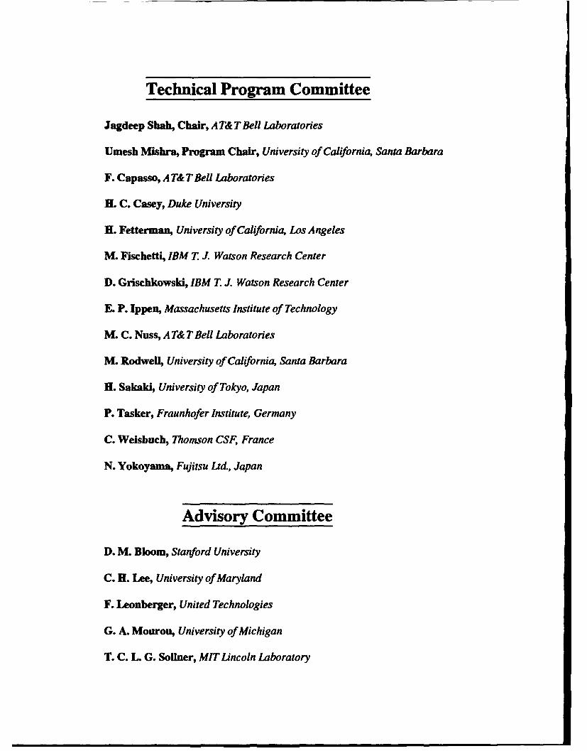
Technical Program Committee
Jagdeep Shah, Chair, AT&T Bell Laboratories
Umesh Mishra, Program Chair, University of California, Santa Barbara
F. Capasso, A T& T Bell Laboratories
H. C. Casey, Duke University
H. Fetterman, University of California, Los Angeles
M. Fischetti, IBM T. J. Watson Research Center
D. Grischkowski, IBM T. J. Watson Research Center
E. P. Ippen, Massachusetts Institute of Technology
M. C. Nuss, A T& T Bell Laboratories
M. Rodwell, University of California, Santa Barbara
H. Sakaki, University of Tokyo, Japan
P. Tasker, Fraunhofer Institute, Germany
C. Weisbuch, Thomson CSF, France
N. Yokoyama, Fujitsu Ltd., Japan
Advisory Committee
D. M. Bloom, Stanford University
C. H. Lee, University of Maryland
F. Leonberger, United Technologies
G. A. Mourou, University of Michigan
T. C. L G. Sollner, MIT Lincoln Laboratory
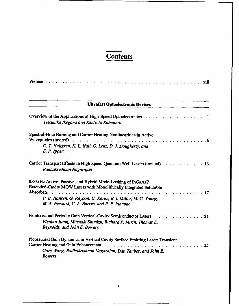
Contents
Preface . .. .. . ... .. .. .. .. .. .. .. .. .. .. .. .. .. .. . . .. .. .. . xiii
Ultrafast Optoelectronic Devices
Overview of the Applications of High-Speed Optoelectronics ....................... 1Tetsuhiko Ikegami and Ken'ichi Kubodera
Spectral-Hole Burning and Carrier Heating Nonlinearities in ActiveWaveguides (invited) ........ ....................................... 6
C. T. Hultgren, K. L Hall, G. Lenz, D. J. Dougherty, andE. P. Ippen
Carrier Transport Effects in High Speed Quantum Well Lasers (invited) .............. 13Radhakrishnan Nagarajan
8.6-GHz Active, Passive, and Hybrid Mode-Locking of InGaAsPExtended-Cavity MQW Lasers with Monolithically Integrated SaturableAbsorbers ........... ............................................ 17
P. B. Hansen, G. Raybon, U. Koren, B. I. Miller, M. G. Young,M. A. Newkirk, C. A. Burrus, and P. P. lannone
Femtosecond Periodic Gain Vertical-Cavity Semiconductor Lasers .................. 21Wenbin Jiang, Mitsuaki Shimizu, Richard P. Mirin, Thomas E.Reynolds, and John E. Bowers
Picosecond Gain Dynamics in Vertical Cavity Surface Emitting Laser: TransientCarrier Heating and Gain Enhancement ....... ............................ 25
Gary Wang, Radhakrishnan Nagarajan, Dan Tauber, and John E.Bowers
v
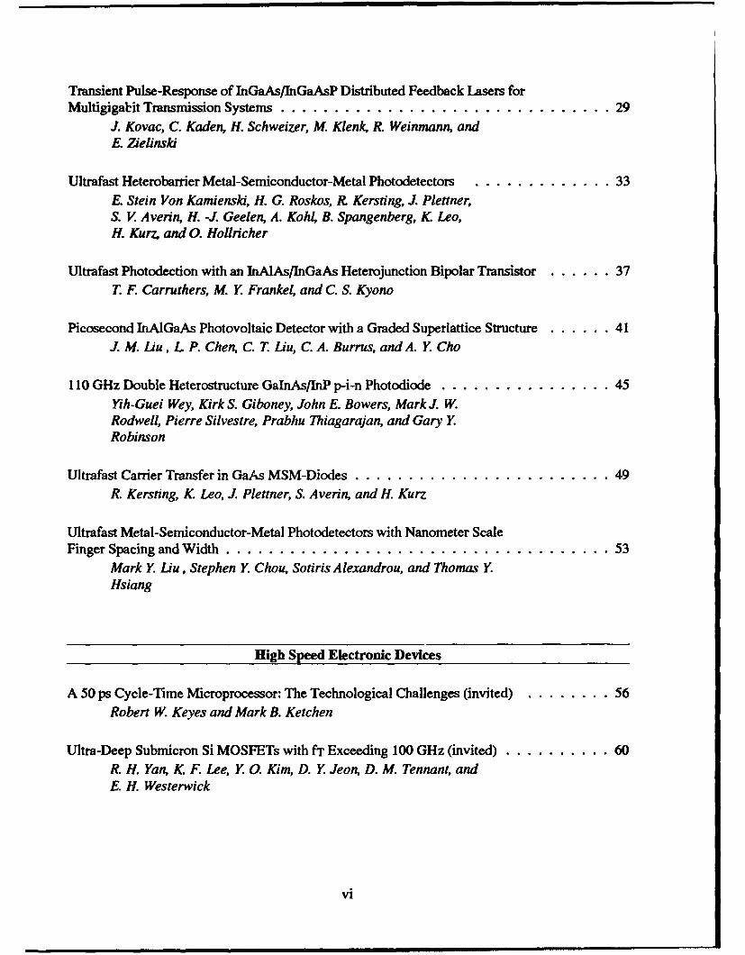
Transient Pulse-Response of InGaAs/InGaAsP Distributed Feedback Lasers forMultigigabit Transmission Systems ....... ............................... 29
J. Kovac, C. Kaden, H. Schweizer, M. Klenk, R. Weinmann, andE. Zielinski
Ultrafast Heterobarrier Metal-Semiconductor-Metal Photodetectors .... ............. 33E. Stein Von Kamienski, H. G. Roskos, i. Kersting, J. Plettner,S. V Averin, H. -J. Geelen, A. Kohl, B. Spangenberg, K. Leo,H. Kurz. and 0. Hollricher
Ultrafast Photodection with an InALAs/InGaAs Heterojunction Bipolar Transistor ....... 37T. F. Carruthers, M. Y Frankel, and C. S. Kyono
Picosecond InA1GaAs Photovoltaic Detector with a Graded Superlattice Structure ...... .41J. M. Liu, L P. Chen, C. T Liu, C. A. Burrus, and A. Y. Cho
110 GHz Double Heterostructure GaInAsJInP p-i-n Photodiode .................... 45Yih-Guei Wey, Kirk S. Giboney, John E. Bowers, Mark J. W.Rodwell, Pierre Silvestre, Prabhu Thiagarajan, and Gary Y.Robinson
Ultrafast Carrier Transfer in GaAs MSM-Diodes .............................. 49R. Kersting, K. Leo, J. Plettner, S. Averin, and H. Kurz
Ultrafast Metal-Semiconductor-Metal Photodetectors with Nanometer ScaleFinger Spacing and Width ........ .................................... 53
Mark Y. Liu, Stephen Y. Chou, Sotiris Alexandrou, and Thomas Y.Hsiang
High Speed Electronic Devices
A 50 ps Cycle-Tiue Microprocessor: The Technological Challenges (invited) .......... 56Robert W. Keyes and Mark B. Ketchen
Ultra-Deep Submicron Si MOSFETs with fT Exceeding 100 GHz (invited) ............ 60R. H. Yan, K. F. Lee, Y. . Kim, D. Y Jeon, D. M. Tennant, andE. H. Westerwick
vi
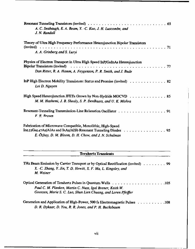
Resonant Tunneling Transistors (invited) ............................ 65A. C. Seabaugh, E A. Beam, Y -C. Kao, J. H. Luscombe, andJ. N. Randall
Theory of Ultra High Frequency Performance Heterojunction Bipolar Transistors(invited) .......... ............................................. 71
A. A. Grinberg and S. Luryi
Physics of Electron Transport in Ultra High Speed InP/GaInAs HeterojunctionBipolar Transistors (invited) ......... .................................. 77
Dan Ritter, R. A. Hamm, A. Feygenson, P. R. Smith, and J. Bude
InP High Electron Mobility Transistors: Status and Promise (invited) ................ 82Loi D. Nguyen
High Speed Heterojunction JFETs Grown by Non-Hydride MOCVD ................ 85M. M. Hashemi, J. B. Shealy, S. P. DenBaars, and U. K. Mishra
Resonant-Tunneling Transmission-Line Relaxation Oscillator ..................... 91F •R. Rrown
Fabrication of Microwave Compatible, Monolithic, High-SpeedIno.53Gao.47As/AIAs and InAs/AlSb Resonant Tunneling Diodes ................... 95
E. Ozbay, D. M. Bloom, D. H. Chow, and J. N. Schulman
Terahertz Transients
THz Beam Emission by Carrier Transport or by Optical Rectification (invited) .......... 99X. -C. Zhang, Y. Jin, T. D. Hewitt, X. F. Ma, L Kingsley, andM. Weiner
Optical Generation of Terahertz Pulses in Quantum Wells ....................... 105Paul C. M. Planken, Martin C. Nuss, Igal Brener, Keith W.Goossen, Marie S. C. Luo, Shun Lien Chuang, and Loren Pfeiffer
Generation and Application of High-Power, 500 fs Electromagnetic Pulses ........... 108D. R. Dykaar, D. You, R. R. Jones, and P. H. Bucksbaum
vii
All-Electronic Generation of Sub-Picosecond Shock-Waves and TheirApplication to a Terahertz Spectroscopy System ............................. 112
Jeffrey S. Bostak, Daniel W. Van Der Weide, Ikuro Aoki, BertramA. Aul" and David M. Bloom
Sub-Picosecond, Terahertz Radiation from High-Intensity Laser Plasmas ............ 116H. Hamster, A. Sullivan, S. Gordon, R W. Falcone, and W. White
Intense THz Beam from Organic Electro-Optic Materials ................... 119X. -C. Zhang, T. -M. Lu, and C. P. Yakymyshyn
New Performance Limits of an Ultrafast THz Photoconductive Receiver ............. 123N. Katzenellenbogen, Hoi Chan, and D. Grischkowsky
Physics of Semiconductors
Application of Ultrafast Optoelectronics to the Characterization of PhotonicCrystals (invited) ........................................ 126
G. Arjavalingan W. M. Robertson, and S. Y. Lin
Ultrafast Optoelectronic Field Changes in GaAs ........................ 129T. Dekorsy, H. Heesel, S. Hunsche, T. Pfeifer, H. Mikkelsen,W. Kintt, K. Leo, and H. Kurz
Velocity Overshoot Dynamics in GaAs up to 200 kV/cm Observed UsingTerahertz Radiation ....................................... 134
J. Son, W, Sha J. Kimn, T. B. Norris, J. F. Whitaker, andG. Mourou
Phase Relaxation Processes of Excitons in Island-Inserted Quantum WellStructures-Suppression of Relaxation and Giant Quantum Beats .................. 138
T. Matsusue, T Saiki, M. Kuwata-Gonokami, H. Akiyama, andH. Sakaki
Observation of Bloch Oscillations in a Semiconductor Superlattice ................. 142Peter Haring Bolivar, Patrick Leisching, Karl Leo, Jagdeep Shah,and Klaus Kdhler
viii
Femtosecond Optical Response of Low Temperature Grown In.53Ga.47As .147
B. C. Tousley, S. M. Mehta, A. L Loba4 P. J. Rodney, P. M.Fauchet, and P. Cooke
Carrier Scattering and Excitonic Effects on Electron-Hole-Pair DiffusionMeasured with Optical Fiber Probing Technique ...... ........................ 151
Hidefumi Akiyama, Toshio Matsusue, and Hiroyuki Sakaki
Novel Sources and Techniques
Passively Mode-Locked Diode-Pumped Solid-State Lasers for OptoelectronicsApplications ........................................... 155
U. Keller, T. H. Chiu, J. F. Ferguson, and K. J. Weingarten
NLTL-Based System for umm-Wave and Sub-mm-Wave Free-SpaceElectromagnetic Measurements ................................. 158
Y. Konishi, M. Case, I. Yu, M. J. W. Rodwell, and M. Kamegawa
Ultrafast Scanning Microscopy ................................. 162S. Weiss, D. Botkin, and D. S. Chemla
Picosecond Electrical Sampling Using a Scanning Force Microscope ............. 166A. S. Hou, F. Ho, and D. M. Bloom
Applications of Time-Lens Optical Systems .......................... 169M. T Kauffman, A. A. Godil, W. C. Banyai, and D. M. Bloom
Femtosecond Field Emission Camera: A Device for Continuously Observing theMotion of Single Adsorbed Atoms and Molecules ....................... 172
Gary M. McClelland, Harry Heinzelmann, and Fumiya Watanabe
(Sub)Millimeter Wave Devices
High Frequency Solid State Sources Using Ultrafast Techniques ............... 175D. V. Plant, D. C. Scott, M. Martin, F. K. Oshita, andH. R. Fetterman
ix
On-Wafer Optoelectronic Techniques for Millimeter-Wave Generation, Control,and Circuit Characterization ........ .................................. 179
Sheng-Lung L Huang, Chi H. Lee, and Hing-Loi A. Hung
Optoelectronic Phase Locking of Microwave Signals up to 4GHz Using aLaser-Diode-Based Electro-Optic Harmonic Mixer ............................ 183
Ci-Ling Pan, Kai-Yuan Tang, and Hsiao-Hua Wu
Photoconductive and Electro-Optic Sampling
Picosecond Detector, Optical Temporal Analyzer, and Free-Standing CircuitProbe (invited) ......... .......................................... 186
J. Nees, S. Williamson, J. Kim, and S. Gupta
Electro-Optic Sampling at 150 fs ................................ 189U. D. Keil and D. R. Dykaar
Low-Temperature MBE Growth of 11-V Materials on Si Substrates .............. 193Michael Y. Frankel, Thomas F. Carruthers, and Bijan Tadayon
Photoconductive Sampling Circuits Using Low-Temperature GaAs InterdigitatedSwitches .......... ............................................. 197
J. Allam, K. Ogawa, J. White, N. de B. Baynes, J. R. A. Cleaver, I.Ohbu, T. Tanoue, and T. Mishima
Transmission Lines
High-Bandwith Transmission Lines Using Low-Temperature-Grown-GaAs-onQuartz .......... .............................................. 201
H. Cheng and J. F. Whitaker
High Speed Limits of Coplanar Transmission Lines ...................... 205U. D. Keil, D. R. Dykaar, A. F. J. Levi, F. Kopf, L N. Pfeiffer,K W. Goossen, S. B. Darack, and K. W. West
x
Subpicosecond Electrical Pulse Generation in GaAs by Nonuniform Illuminationof Series and Parallel Transmission-Line Gaps .............................. 209
Sotiris Alexandrou, Chia-Chi Wang, Roman Sobolewski, andThomas Y. Hsiang
Ultrafast Probes of Materials/Devices/Circuits
Supbicosecond GaAs Wafer Probe System ................................. 213M. S. Shakouri, A. Black, B. A. Auld, and D. M. Bloom
Highly Reproducible Optoelectronic Wafer Probes with Fiber Input ................ 216M. D. Feuer, S. C. Shunk, M. C. Nuss, P. R. Smith, H. H. Law, andC. A. Burrus
Electro-Optic Sampling of High Speed Nonlinear Devices ................... 220Kok Wai Chang and Wayne V. Sorin
120-GHz-Bandwidth Characterization of Microwave Passive Devices UsingExternal Silicon-On-Sapphire Photoconductive Sampling Probe ................... 224
J. Kim, J. Son, S. Wakana, J. Nees, S. Williamson, J. Whitaker,and G. Mourou
Superconductors
Optical Control of High Speed Circuit Using Picosecond High TemperatureSuperconductor Opening Switches ....... ............................... 228
Yuan-Qun Liu, Yi-Sern Lai, Wei-lou Cao, Chi H. Lee, S. N. Mao,X. X. Xi, T Venkatesan, Zhi- Yuan Shen, Philip Pang, Dennis J.Kountz, and William L Holstein
Response of a Nb/A1203/Nb Tunnel Junction to Picosecond Electrical Pulses .......... 231C. Karadi, S. Verghese, C. A. Mears, J. Orenstein, P. L Richards,and A. T Barfknecht
Ultrafast Optical and Optoelectronic Response of Y-Ba-Cu-O .................... 234T. Gong, L X. Zheng, Y. Kostoulas, W. Xiong, W. Kula, K. B.Ucer, Roman Sobolewski, and P. M. Fauchet
xi
Terahertz Spectroscopy of Superconducting Thin Film Bao.6K0.4BiO3 ............ 238Yongqian Liu, John F. Whitaker, and Christine E Platt
Ultrafast Quasiparticles Dynamics in High-Temperature Superconductors ............ 242W. Albrecht, Th. Kruse, K Leo, and H. Kurz
Author Index ........... .......................................... 246
xii
Preface
This volume is comprised of papers that were presented at the Fifth Topical Meeting on UltrafastElectronics and Optoelectronics (formerly Picosecond Electronics and Optoelectronics), held in SanFrancisco, January 23-25, 1993. The purpose of this topical meeting, since its inception in 1985,has been to foster greater interaction between researchers in the electronics and optoelectronicscommunities who share a common interest in the physics and technology of ultrafast electronicsand optoelectronics devices, their multigigahertz applications, and ultrafast measurement tech-niques. The number of abstracts submitted to this meeting was considerably larger than for theprevious meetings, indicating the appeal of this interdisciplinary approach and the growingimportance of this field. This preface serves as a summary and a guide to these Proceedings.
Ultrafast Optoelectronic Devices is concerned with high speed electronic devices and presentsa discussion of the state-of-the-art devices such as resonant tunneling transistors, bipolar transistorsand high electron-mobility transistors, and >100 GHz Si MOSFETs.
High Speed Electronic Devices discusses state-of-the-art optoelectronic devices such as lasersand detectors. Gain dynamics and carrier transport in semiconductor lasers, mode-locking of lasers,integrated laser-modulators, vertical cavity lasers, metal-semiconductor-metal photodetectors, HBTphotodetectors, and photovoltaic photodetectors are some of the topics discussed in this section.
Terahertz Transients is concerned with the physics and technology of generation and detectionof terahertz transients from semiconductors, and applications of terahertz transients generated byhigh power femtosecond lasers.
Physics of Semiconductors covers physics of semiconductors. This part includes a discussion ofphotonic bandgap, high field transport, Bloch oscillations, and coherent effects in semiconductornanostructures.
Novel Sources and Techniques covers a discussion of novel sources, such as mode-lockeddiode-pumped solid-state lasers, as well as novel techniques such as high spatial and temporalresolution probes using scanning force microscopes, and time-reversal using a temporal imagingsystem.
(Sub)Millimeter Wave Devices covers generation, and control of millimeter- and submillime-ter-wave radiation from solid state sources using picosecond lasers, and applications of such sourcesfor circuit characterization.
Photoconductive and Electro-Optic Sampling covers recent advances in the field of photocon-ductive and electro-optic sampling techniques and materials; Transmission Lines covers recentadvances in generation and propagation of sub-picosecond pulses using transmission lines; and
xii1
Ultrafast Probes of Materials/Devices/Circuits covers recent advances in ultrafast probes of mate-rials, devices, and circuits.
The final section, Superconductors, covers the interaction of ultrashort pulses with superconduc-tors, and its application in the optical control of an electrical circuit.
We gratefully acknowledge the grants from the Air Force Office of Scientific Research(AFOSR), the Office of Naval Research (ONR), and the National Science Foundation (NSF), whichprovided the funding for the meeting. We also take this opportunity to thank the members of theAdvisory Committee and the Technical Program Committee for their substantial contributions tothe success of the meeting. Finally, we would like to thank Monica Malouf and Ellen Murphy ofthe Optical Society of America for a thoroughly professional management of the meeting.
Jagdeep ShahAT&T Bell Laboratories
Umesh MishraUniversity of California, Santa Barbara
xiv
Ultrafast Optoelectronic Devices
Overview of the Applications of High-Speed Optoelectronics
Tetsuhiko IkegamiN7T R&D Headquarters, 1-1-7 Uchisaiwaicho, Chiyoda-Ik4 Tokyo 100, Japan
Ken'ichi KuboderaNTT Interdisciplinary Research Laboratories, 3-9-11 Midoricho, Musashino-shi, Tokyo 180, Japan
ABSTRACT small solder bump connection technique
Picosecond optical devices such as mnono- which allows precise chip alignment and gives
lithic and hybrid OEICs, LiNbO 3 modula- low wire inductance and stray capacitance
tors and switches, and all-optical picosec- [4]. A 3-dB bandwidth of more than 22 GHz
ond switches are reviewed for future high- and a noise current of 19.4 pA/Hz1/ 2 were
bit-rate optical transmission and signal pro- obtained by this module. A 10-Gb/s op-
cessing. tical CPFSK heterodyne detection experi-ment has been conducted using this device
1. Introduction [5].
Monolithically integrated OEIC devicesApplications of high-speed opto-electronics have been also investigated extensively. Fig-are important technologies not only for the ure 2 shows the recently reported receiversophistication of today's high-bit-rate long- OEIC consisting of a p-i-n photodiode andhaul optical communication systems, but also a high electron mobility transistor (HEMT),for the realization of future ultra-high-bit- fabricated using Si-planar-doping and Be-rate optical signal processing systems [1-3]. ion implantation techniques [6]. The receiverKey devices are hybrid or monolithic OE- showed a 3-dB-down bandwidth of a 8 GHzICs, LiNbO 3 modulators and switches, mode- and was capable of operation with a 10-locked LDs, and all-optical picosecond switch- Gb/s NRZ signal. Since monolithic OEICes such as bistable memory LDs, and ultra- devices have advantages of reduced cost andfast nonlinear-optical switches. reliable performance, they are especially suit-
able for optical interconnection, switchingElectronics systems, and optical subscriber networks.
A practical transmitter for up to the 10-A. Sophistication in Todays Communication Gb/s optical signal could be a combination
Systems of a single-mode DFB LD and a LiNbO3
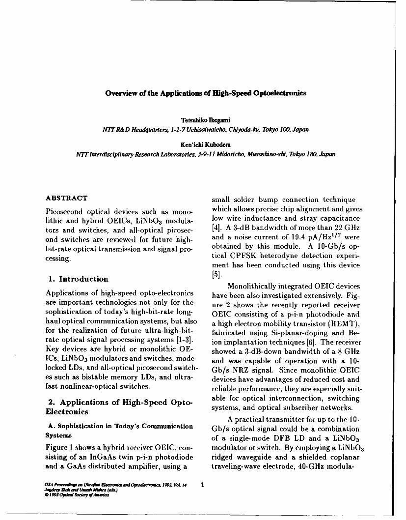
Figure 1 shows a hybrid receiver OEIC, con- modulator or switch. By employing a LiNbO 3sisting of an InGaAs twin p-i-n photodiode ridged waveguide and a shielded coplanarand a GaAs distributed amplifier, using a traveling-wave electrode, 40-GHz modula-
0SA PoceWVpc Ub, rq~F ecvOpamloekcfiWk 1993. VoL, 14.Jqdeep Skah .nd IMunk Midum (ek)0 1993 Op~kal Soikty t'fAaunim
2 Ultrafast Electronics and Optoelectronics
r -------------------------- I ~--Shielding plane
TwinPIN , ~CPW electrode
Photodiode"': SiO 2 buffer layerw~j z-cut LiNbO3 substrate
fL::jEtched regions Ti-diffused waveguides-.- oCoplanar Waveguide
IL--------------------------------J4 LýDjstributed Amplifier ______________
I_ 5_Solder BumpConnection b
-~.5 0.0 0 00
-15 - 0
(D 0 measuredIn 0 -15 -calculated
10 -2 5 10 15 20 25 30 35 40
~ -20Frequency (GHz)S 2 6 10 14 18 22
Frequency (GHz) Figure 3. LiNbO3 optical miodulator with 40 (Alzbandwidth [7].
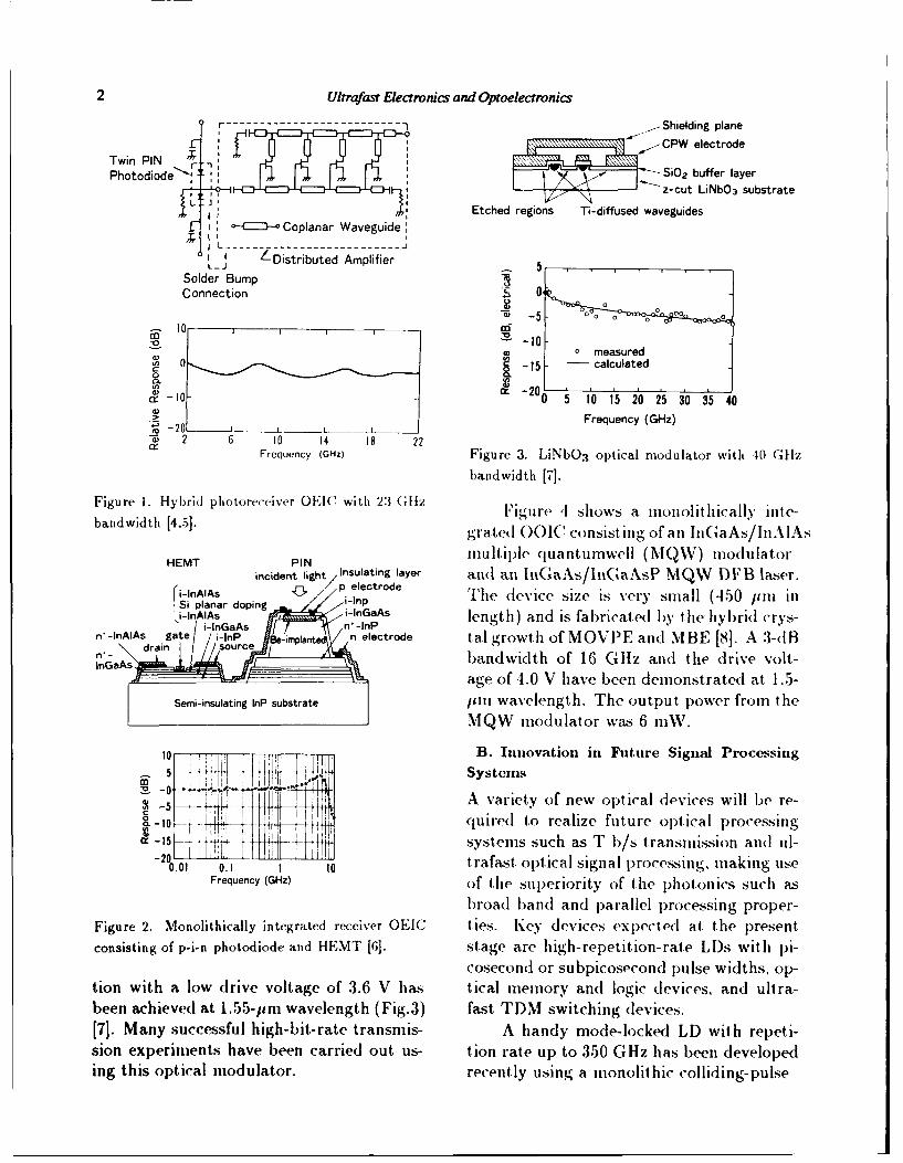
Figure 1. Hybrid photorectiver OEIAC with 23 GlIlz Figuire I1 shows a mnonolithically inte-bandidt [45].grated 00IC. consisting of an InGaAs/InAlAs
HEMT PIN m~ultiple qua~ntumwell (MNQW) modulator
.incident light insulating layer and an linGaAs,/iG'a~sP MQW DFB laser.
l i-In~l~s p electrodeTedeieszisvrsml(40pnISi planar doping i-Inp Tedvc iei ey ml 40piigae -ln~AAs ie-ir~lan length) and is fa~bricat ed by thfe hybrid crys-
AlA. te n Beimplnt nelecrode tal growth l of M OV PE and M BE [8]. A .3-d Bn'- rai sorcebandwidth of 16 Gllz an(1 the drive volt.-In~aAs Itage of 4.0 V have been demonstrated at. 1.5-
Semi-insulating lnP substrate pmi wavelength. The output, power from theMIQW modulator was 6 niW.
16 B. Innovation in Future Signal Processing
*v -0~Systems
-5 Il0 A variet~y of new optical devices will be re-.- 10 ~.-qired to realize future optical processing
-I 5~ 4 systems such as T' b/s transmission an] ulI-
0.0f 0.1 1 to tra~fast. opt.ical signal processing.,,mkn SFrequency (G~z) of the superiority of t~he photon ics such as
broad band and p~arallel p~rocessing proper-
Figure 2. Monolithically integrated receiver OEIC ties. Key devices expected at. the present,consisting of p-i-n photodiode and HEMT [6]. st~age are high-repetit, ion- rat e LDs with pi-
cosecondi or subpicosecond pulse widths, op-tion with a low drive voltage of 3.6 V has tical memory and logic devices, and ultra-been achieved at 1.55-pim wavelength (Fig.3) fast TDM switching devices.[7]. Many successful high-bit-rate transmis- A handy mode-locked LD wit~h repeti-sion experiments have been carried out. us- tion rate up to 350 GINz has been developeding this optical modulator. recently using a monolithic colliding-pulse
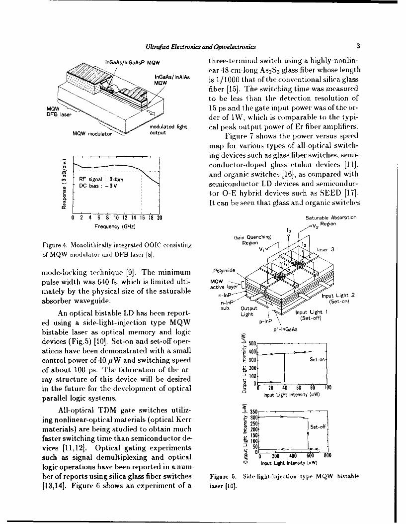
Uhtrafast Electronics and Optoelectronics 3
InGaAs/InGaAsP MQW three-terminal switch using a highly-nonlin-ea~r 48 cmi-long AS2 S3 glass fiber whose length
InGaAs/InAlAs is 1/1000 that of the conventional silica glass
fiber [15]. The switching time was measuredto be less than the detection resolution of
MQW' 15 ps and thie gate input power was of the or-DFB laser • der of IW, which is comparable to the typi-
modulated light cal peak output power of Er fiber amplifiers.MQW modulator output Figure 7 shows the power versus speed
map for various types of all-optical switch-ing devices such as glass fiber switches, semi-conductor-doped glass etalon devices [11].
RF signal 0dbm and organic switches [16], as compared with
•, DC bias -3V semiconductor LD devices and semiconduc-
0 : tor O-E hybrid devices such as SEED [17].It can be seen that glass and organic switches
0 2 4 6 8 10 1'2 1'4 16 1'8 20 Saturable AbsorptionFrequency (GHz) 13 V2 Region
Gain Quenching
Figure 4. Monolithically integrated OOIC consisting Region "" la 3
of MQW modulator and DFB laser k].
mode-locking technique [9]. The minimum Polyimide v 2
pulse width was 640 fs, which is limited ulti- MQW
mately by the physical size of the saturable active layern-lnP••
'/ input Light2
absorber waveguide. n-lnP- (Set-on)sub. OutputI
An optical bistable LD has been report- Light nput Light - 1ed using a side-light-injection type MQW p-Ins
bistable laser as optical memory and logic p.
devices (Fig.5) [10]. Set-on and set-off oper- -_500____, ___._,
ations have been demonstrated with a small C 400control power of 40 ttW and switching speed 300° Set-on-
of about. 100 ps. The fabrication of the ar- t 200 --J 100-
ray structure of this device will be desired C 0• . - . .
in the future for the development of optical 01 0 20 40 60 80 100
parallel logic systems. Input Light Intensity (mW)
All-optical TDM gate switches utiliz- 350ing nonlinear-optical materials (optical Kerr 300
materials) are being studied to obtain much • 200 tS150faster switching time than semiconductor de- 1500
vices [11,12]. Optical gating experiments 50
such as signal demultiplexing and optical 0 200 400 600 800
logic operations have been reported in a num- 0 Input Light Intensity (vW)
ber of reports using silica glass fiber switches Figure 5. Side-light-injection type MQW bistable
(13,14]. Figure 6 shows an experiment of a laser (10].
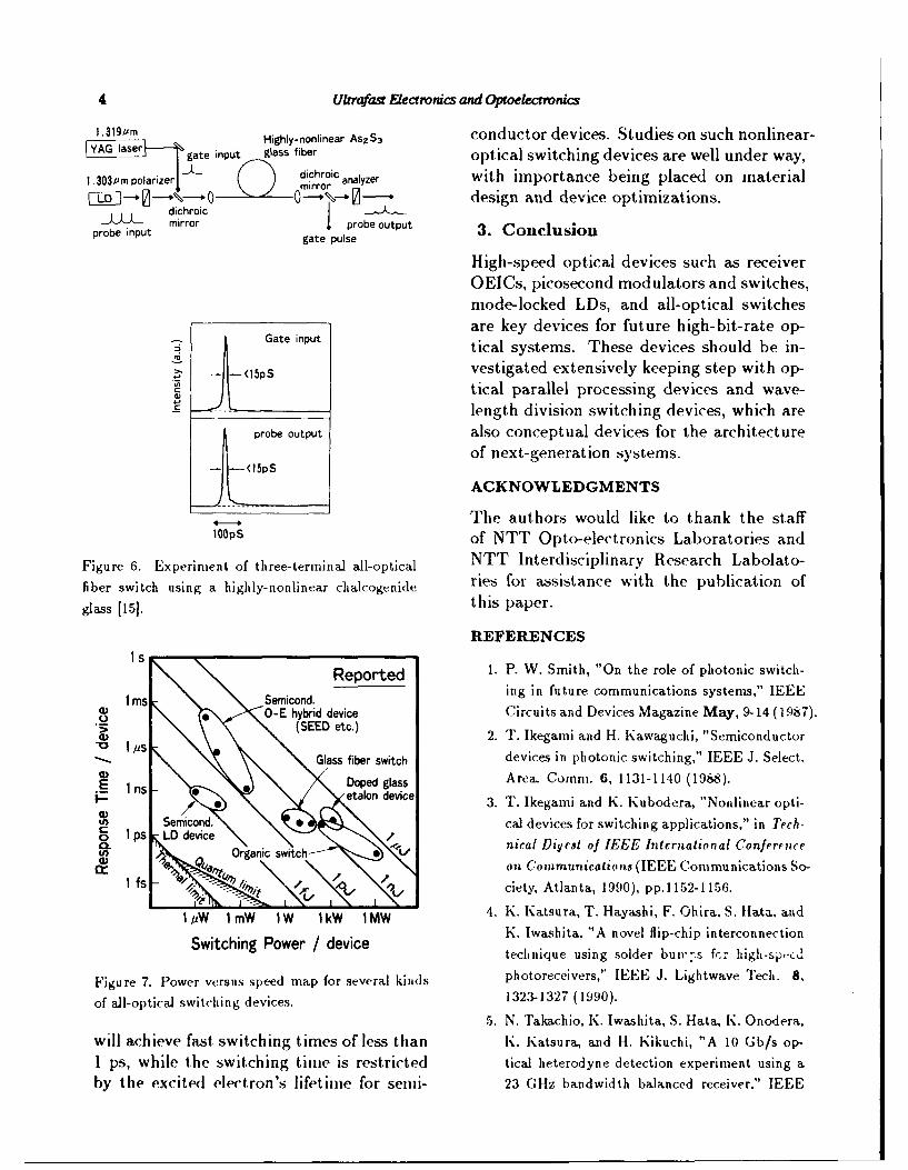
4 Ultrafast Eectronics and Oproelectronics
1.319pm Highly-nonlinear AsS 3 conductor devices. Studies on such nonlinear-SY G aser I•-
gate input glass fiber optical switching devices are well under way,
i'303pmpolarizer I ichroc anal yzer with importance being placed on materialSL_- -----* O %-- -- design and device optimizations.
dichroicproberinput probe output 3* Conclusion_J U mirror poeot uprobe input gate pulse
High-speed optical devices such as receiverOEICs, picosecond modulators and switches,mode-locked LDs, and all-optical switchesare key devices for future high-bit-rate op-
?at tical systems. These devices should be in-
-1-<l5pS vestigated extensively keeping step with op-tical parallel processing devices and wave-
----- length division switching devices, which areprobe output also conceptual devices for the architecture
of next-generation systems.
ACKNOWLEDGMENTS
The authors would like to thank the staffloops of NTT Opto-electronics Laboratories and
Figure 6. Experiment of three-terminal all-optical NTT Interdisciplinary Research Labolato-fiber switch using a highly-nonlinear clialcogenide ries for assistance with the publication of
glass [15]. this paper.
REFERENCESIs
Reported 1. P. W. Smith, "On the role of photonic switch-
Ims Semicond. ing in future communications systems," IEEE)" O-E hybrid device Circuits and Devices Magazine May, 9-14 (1987).>• (SEED etc.)( 2. T. Ikegami and H. Kawaguchi, "Semiconductor
Glass fiber switch devices in photonic switching," IEEE J. Select.
t nsDoped glass Area. Comm. 6, 1131-1140 (1988).1.• detalon device 3. T. Ikegami and K. Kubodera, "Nonlinear opti-
Semicond. cal devices for switching applications," in Tech-- I ps LD device_, nical Digest of IEEE International Conffrrncei Organic switch0
CC I a- ont Communications (IEEE Communications So-ifs "ciety, Atlanta, 1990), pp.1152-1156.
1AMW I mW IW IkW IMW 4. K. Katsura, T. Hayashi, F. Ohira, S. Hata., andK. Iwashita, "A novel flip-chip interconnectiontechnique using solder buir-ps fkr high-sp,'cd
Figure 7. Power versus speed map for several kinds photoreceivers," IEEE J. Lightwave Tech. 8,
of all-optical switching devices. 1323-1327 (1990).
5. N. Takachio, K. Iwashita, S. Hata, K. Onodera,will achieve fast. switching times of less than K. Katsura, and H. Kikuchi, "A 10 Gb/s op-
1 ps, while the switching time is restricted tical heterodyne detection experiment using aby the excited electron's lifetime for senmi- 23 GHz bandwidth balanced receiver," IEEE
Ultrafast Electrotncs and Optoelectronics 5
Trans. Microwave Theory Tech. 38, 1900-1905 Verlag, Berlin, 1990), pp. 23-29.
(1990). 12. K. Kubodera, "Picosecond switching devices
6. Y. Akahori, Y. Akatsu, A. Kohzen, and J. Yoshi- and materials," in TechnicalDigest of 4th Opto-
da, "10-Gb/s high-speed monolithically inte- electronics Conference (IEICE, Makuhari, Chi-
grated photoreceiver using InGaAs p-i-n PD ba, 1992), pp.ll0-111.
and planar doped InAlAs/InGaAs HEMT's," 13. B. P. Nelson, K. J. Blow, P. D. Constantine,!EEE Photonics Tech. Lett. 4, 754-756 (1992). N.J. Doran, J. K. Lucek. I. W. Marshall, and
7. K. Noguchi, 0. Mitomi, and M. Yanagibashi, K. Smith, "All optical Gbit/s switching using
"40 GHz Ti:LiNbO3 optical modulator with nonlinear optical loop mirror," Electron. Lett.
driving voltage of 3.6 V," in Technical Digest of 27, 704-705 (1991).
4th Optoelectronics Conference (IEICE, Maku- 14. M. Jinno and T. Matsumoto, "Ultrafast all-
hari, Chiba, 1992), pp.PD4-5. optical logic operations in a nonlinear Sagnac
8. K. Wakita, I. Kotaka, H. Asai, M. Okamoto, interferometer with two pump pulses," in Tech-
Y. Kondo, and M. Naganuma, "High-speed and nical Digest of Conference on Optica Fiber Corn-
low-drive-voltage monolithic multiple quantum- munication (OSA, 1991) p.48.
well modulator/DFB laser light source," IEEE 15. M. Asobe, T. lanamori, and K. Kubodera,
Photonics Tech. Lett. 4, 16-18 (1992). "Ultrafast all-optical switching using highly non-
9. Y. K. Chen, M. C. Wu, T. Tanbun-Ek, R. A. linear chalcogenide glass fiber," IEEE Photon-
Logan, and M. A. Chin, "Subpicosecond mono- ics Tech. Lett. 4, 362-365 (1992).
lithic colliding-pulse mode-locked multiple quan- 16. P. D. Townsend, J. L. Jackel, G. L. Baker,
tum well lasers," Appl. Phys. Lett. 58, 1253- J. A. Shelburne, and S. Etemad, "Observation
1255 (1991). of nonlinear optical transmission and switch-
10. H. Uenohara, Y. Kawamura, H. Iwamura, K. ing phenomena in polydiacetylene-based direc-
Nonaka, H. Tsuda, and T. Kurokawa, "Side- tional couplers," Appl. Phys. Lett. 55, 1829-
light-injection MQW bistable laser using sat- 1831 (1989).
urable absorption and gain quenching," Elec- 17. A. L. Lentine, F. B. Mccormick, R. A. Novotny,
tron. Lett. 28, 1973-1974 (1992). L. M. F. Chirovsky, L. A. D'asaro, R. F. Kopf,
11. K. Kubodera, "Nonlinear optical devices for J. M. Kuo, and G. D. Boyd, "A 2 kbit array
photonic switching," in Photonic Switching II, of symmetric self-electrooptic effect devices,"
K. Tada and H. S. Hinton, eds. (Springer- IEEE Photonics Tech. Leti 2, 51-53 (1990).
Spectral-Hole Burning and Carrier HeatingNonlinearities in Active Waveguides
C. T. Hultgren, K. L Hall, G. Lenz, D. J. Dougherty, andE. P. Ippen
Department of Electrical Engineering and Computer Science andResearch Laboratory of Electronics, Massachusetts Institute of Technology,
Cambridge, Massachusetts 02139
Abstract Background
Studies of active waveguides with short optical pulses Pump-probe experiments are valuable because theyprovide information about fundamental carrier dy- provide direct, time domain measurements of ultra-namics and nonlinear processes relevant to high speed fast nonlinearities in active waveguides. Generally,modulation and optical communication. We investi- in these experiments, a beam of short pulses (typi-gate these dynamics in AlGaAs amplifiers around 0.8 cally - 100 fs) is split into two, a strong pump beam,um and InGaAsP amplifiers around 1.5 jim using op- and a weak probe beam. After traveling separate,tical pulses approximately 100 fs in duration. Novel but approximately equal paths, the two beams aremeasurement techniques are employed to elucidate recombined collinearly and are coupled to the activecontributions to both gain and refractive index non- region of a diode laser. After propagating throughlinearities. By identifying a delay in the onset of the diode, the probe beam is selected for detection.carrier heating, we are able to observe an ultrafast A variable stepping stage in the pump path is useddynamic we attribute to spectral-hole burning, to set the delay between pump and probe pulses,
and the change in probe transmission or phpe isIntroduction measured as a function of pump-probe delay.
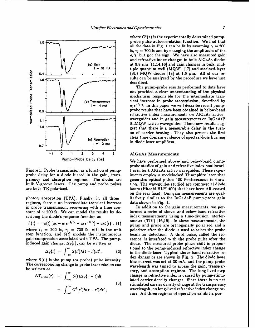
Fig. 1 shows the measured change in probe trans-Semiconductor diode lasers offer potential for high- mission as a function of pump-probe delay for a bulkspeed optical amplification and all-optical switching. InGaAsP diode laser amplifier biased in the gain,The realization of such devices, however, will require transparency and absorption regimes [12,15]. Theknowledge of their ultrafast gain and refractive in- regimes of operation are distinguished by the long-dex dynamics. These dynamics have been studied lived change in probe transmission due to stimulatedpreviously in the frequency domain via nondegener- emission (gain) or absorption (absorption) of theate four-wave mixing [1-5[ and high-speed modula- pump. At the transparency point, there are no nettion response [6-8] experiments. Gain saturation [9] stimulated transitions and no step change in probeand spectral distortions [10] of short pulses traveling transmission. Any transient effect due to spectral-through active waveguides have also been investi- hole burning would be expected to have a very fastgated. With two pulse pump-probe experiments we time constant and an amplitude that scaled with thehave studied the temporal dynamics of active wave- size and sign of the step. However, the nonlinear dy-guides directly, on a femtosecond timescale [11-14]. namics we observe all appear to have the same signIn this paper, we present the results of our most in the three regimes of operation. For instance, allrecent studies of gain and refractive index nonlin- three regimes show a gain compression that recov-earities in both AIGaAs and InGaAsP active wave- ers with a 700 fs time constant. This compression isguides. In each material system, we identify ultra- due to a heating of the carrier distribution (carrierfast effects due to two-photon absorption, carrier heating) via free carrier absorption and stimulatedheating, spectral-hole burning, and an instantaneous transitions. There is an instantaneous gain compres-refractive index nonlinearity. sion in all three regimes that is associated with two-
oSA Proceedns on Ukboft ElearoucndO Oooieaomn 1993. VoL 14 6Jagdeep Shah mad Umesh Mahra (edk)0 1993 Optcal Society ofAmerica
Ultrafast Electronics and Optoelectronics 7
where G2 (r) is the experimentally determined pump-1.0.• probe pulse autocorrelation function. We find that~all the data in Fig. 1 can be fit by assuming T1 = 200
fs, r2 = 700 fs and by changing the amplitudes of theai's, but not the sign. We have also measured gainand refractive index changes in bulk AlGaAs diodes
(a) Gain at 0.8 pAm [11,14,161 and gain changes in bulk, mul-l- 18 mA tiple quantum well (MQW) [17] and strained-layer
. 0.(SL) MQW diodes [18] at 1.5 jam. All of our re-1. 0 suits can be analyzed by the procedure we have just1.0--
described.a The pump-probe results performed to date have
not provided a clear understanding of the physicalmechanism responsible for the intermediate tran-
(b) Transparency sient increase in probe transmission, described byI 14 mA a,/e-Y/. In this paper we will describe recent pump-
om 0.s probe results that have been obtained in below-bandaI _ I I I _ I refractive index measurements on AIGaAs active0 1.1 waveguides and in gain measurements on InGaAsPz SLMQW active waveguides. These new results sug-
1.0- •gest that there is a measurable delay in the turn-on of carrier heating. They also present the firstclear time domain evidence of spectral-hole burning
(.) Absorption in diode laser amplifiers.I 1rf I | I0.7
-1 0 1 2 3 4 5 AIGaAs Measurements
Pump-Probe Delay (ps) We have performed above- and below-band pump-
probe studies of gain and refractive index nonlineari-Figure 1. Probe transmission as a function of pump- ties in bulk AIGaAs active waveguides. These exper-probe delay for a diode biased in the gain, trans- iments employ a modelocked Ti:sapphire laser thatparency and absorption regimes. The diodes are generates optical pulses 100 femtoseconds in dura-bulk V-groove lasers. The pump and probe pulses tion. The waveguides studied are commercial diodeare both TE polarized. lasers (Hitachi HLP1400) that have been AR-coated
on the rear facet. Our gain measurements are qual-photon absorption (TPA). Finally, in all three itatively similar to the InGaAsP pump-probe gainregimes, there is an intermediate transient increase data shown in Fig. 1.in probe transmission, recovering with a time con- In addition to the gain measurements, we per-stant of - 200 fs. We can model the results by de- formed a series of above- and below-band refractivescribing the diode's response function as index measurements using a time-division interfer-
= u(t) [ao + ale-/"- a2et/2 a(t) ,(1) ometer (TDI) [16,19]. In these measurements, theh(t) tpump and probe are orthogonally polarized and a
where rl = 200 fs, r2 = 700 fs, u(t) is the unit polarizer after the diode is used to select the probestep function, and 6(t) models the instantaneous beam for detection. A third pulse, called the ref-gain compression associated with TPA. The pump- erence, is interfered with the probe pulse after theinduced gain change, Ag(t), can be written as diode. The measured probe phase shift is propor-
,o- tional to the pump-induced refractive index changeAg(t) = ] S(t')h(t - t')dt', (2) in the diode laser. Typical above-band refractive in-
-o dex dynamics are shown in Fig. 2. The diode laserwhere S(t') is the pump (or probe) pulse intensity, bias current was set at 30 mA, and the pump-probeThe corresponding change in probe transmission can wavelength was tuned to access the gain, transpar-be written as ency, and absorption regimes. The long-lived step
ATprobe(r) = S(t)Ag(r - t)dt change in refractive index is caused by pump-stimu-00ac lated carrier density changes. Since there is no net
0c (3) stimulated carrier density change at the transparency= G2(r')h(r - r')dr', wavelength, no long-lived refractive index change oc-
-c curs. All three regimes of operation exhibit a pos-
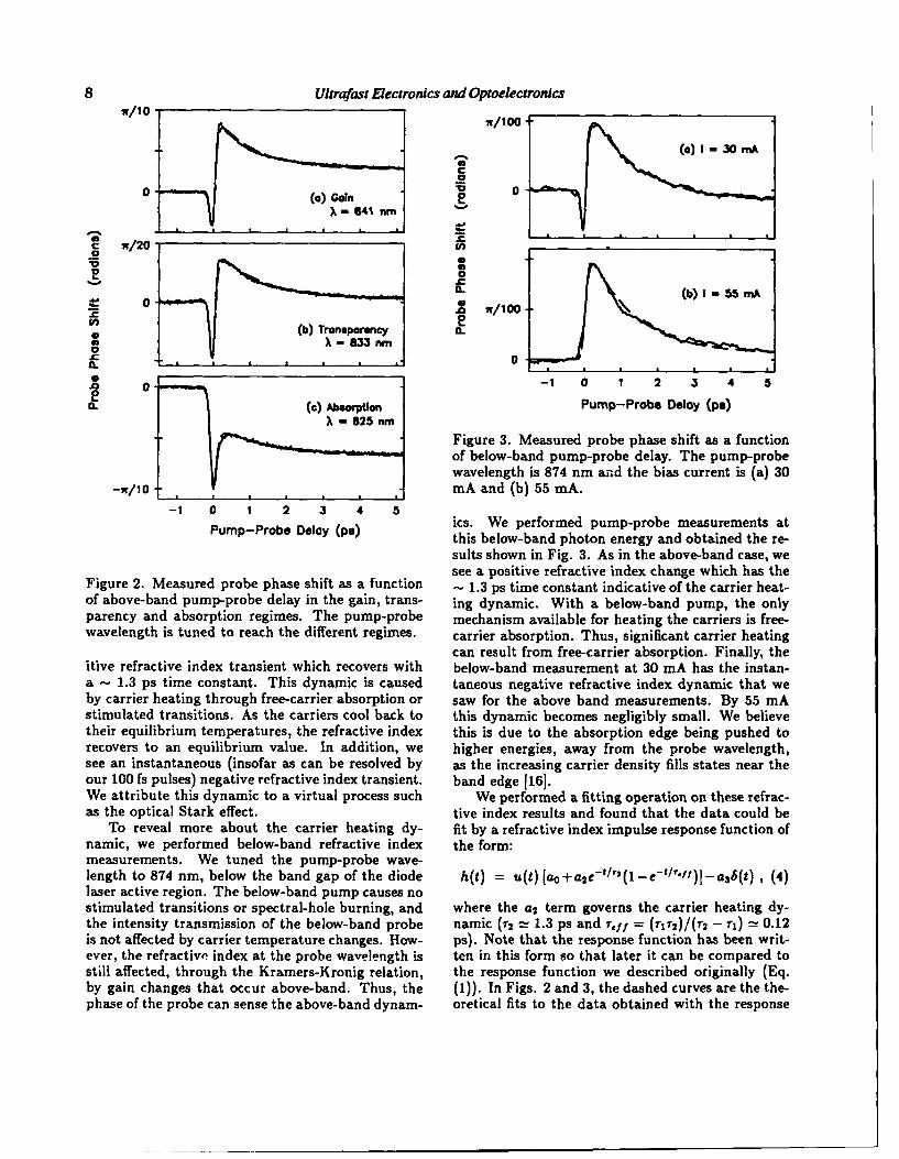
8 Ultrafast Electronics and Optoelectronicsr/t 0 w,1/ o
(a) -30 mAC
0 V 0
c w/20 I0
0v 3
.22i0 (b) Tr1narency 0.
m~ 6," 33 nm000
I_ _ _ _ _ _ _ _ 0 _
0- - -1 0 1 2 3 4 5
Q. (c) Aborption Pump-Probe Delay (p.)X, - 825 nm
Figure 3. Measured probe phase shift as a functionof below-band pump-probe delay. The pump-probewavelength is 874 nm an-d the bias current is (a) 30
-/0 . . . .mA and (b) 55 mA.
-1 0 1 2 3 4 5ics. We performed pump-probe measurements at
Pump-Probe Delay (pa) this below-band photon energy and obtained the re-
sults shown in Fig. 3. As in the above-band case, wesee a positive refractive index change which has the
Figure 2. Measured probe phase shift as a function - 1.3 ps time constant indicative of the carrier heat-of above-band pump-probe delay in the gain, trans- ing dynamic. With a below-band pump, the onlyparency and absorption regimes. The pump-probe mechanism available for heating the carriers is free-wavelength is tuned to reach the different regimes. carrier absorption. Thus, significant carrier heating
can result from free-carrier absorption. Finally, theitive refractive index transient which recovers with below-band measurement at 30 mA has the instan-a - 1.3 ps time constant. This dynamic is caused taneous negative refractive index dynamic that weby carrier heating through free-carrier absorption or saw for the above band measurements. By 55 mAstimulated transitions. As the carriers cool back to this dynamic becomes negligibly small. We believetheir equilibrium temperatures, the refractive index this is due to the absorption edge being pushed torecovers to an equilibrium value. In addition, we higher energies, away from the probe wavelength,see an instantaneous (insofar as can be resolved by as the increasing carrier density fills states near theour 100 fs pulses) negative refractive index transient, band edge 16].We attribute this dynamic to a virtual process such We performed a fitting operation on these refrac-as the optical Stark effect. tive index results and found that the data could be
To reveal more about the carrier heating dy- fit by a refractive index impulse response function ofnamic, we performed below-band refractive index the form:measurements. We tuned the pump-probe wave-length to 874 nm, below the band gap of the diode h(t) = u(t)[ao+a 2Ct'/2(1-etl"I)I-as6(t) , (4)laser active region. The below-band pump causes nostimulated transitions or spectral-hole burning, and where the a2 term governs the carrier heating dy-the intensity transmission of the below-band probe namic (r2 t- 1.3 ps and TE,, = (T1r 2 )/(T2 - ri) L- 0.12is not affected by carrier temperature changes. How- ps). Note that the response function has been writ-ever, the refractive index at the probe wavelength is ten in this form so that later it can be compared tostill affected, through the Kramers-Kronig relation, the response function we described originally (Eq.by gain changes that occur above-band. Thus, the (1)). In Figs. 2 and 3, the dashed curves are the the-phase of the probe can sense the above-band dynam- oretical fits to the data obtained with the response
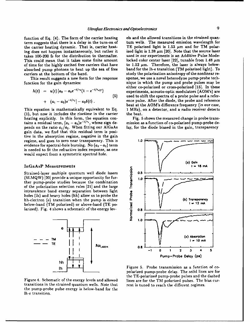
Ultrafast Electronics and Optoelectronics 9
function of Eq. (4). The form of the carrier heating els and the allowed transitions in the strained quan-term suggests that there is a delay in the turn-on of turn wells. The measured emission wavelength forthe carrier heating dynamic. That is, carrier heat- TE polarized light is 1.53 Am and for TM polar-ing does not happen instantaneously, but rather it ized light is 1.38 Am 1201. Note that the source lasertakes 100-200 fs for the distribution to thermalize. used in our experiments is an Additive Pulse Mode-This could mean that it takes some finite amount locked color center laser [221, tunable from 1.48 pmof time for the highly excited free carriers that have to 1.52 Am. Therefore, the laser is always below-absorbed pump photons to heat up the sea of free band for the lh-e transition (TM polarized light). Tocarriers at the bottom of the band. study the polarization anisotropy of the nonlinear re-
This result suggests a new form for the response sponse, we use a novel heterodyne pump-probe tech-function for the gain dynamics: nique in which the pump and probe pulses may be
either co-polarized or cross-polarized [15]. In theseh(t) = u(t) [a0 - aze-t/2(1 - e-t/T'I) experiments, acousto-optic modulators (AOM's) are
(5) used to shift the spectra of a probe pulse and a refer-+ (a, - a2)e-t/T1 - a 36(t), ence pulse. After the diode, the probe and reference
beat at the AOM's difference frequency (in our case,This equation is mathematically equivalent to Eq. 1 MHz), on a detector, and a radio receiver detects(1), but now it includes the risetime in the carrier the beat.heating explicitly. In this form, the equation con- Fig. 5 shows the measured change in probe trans-tains a residual term, (a, - a 2 )e-t/v', whose sign de- mission as a function of co-polarized pump-probe de-pends on the ratio a1 /a 2. When fitting our AIGaAs lay, for the diode biased in the gain, transparencygain data, we find that this residual term is posi-tive in the absorption regime, negative in the gainregime, and goes to zero near transparency. This is 1.0.evidence for spectral-hole burning. No (a, - a2 ) termis needed to fit the refractive index response, as onewould expect from a symmetric spectral hole.
(a) rCoinInGaAsP Measurements I - 18 rnA
Strained-layer multiple quantum well diode lasers a 0.5
(SLMQW) [201 provide a unique opportunity for fur- 1.0 - - --
ther pump-probe studies because the combination Cof the polarization selection rules [211 and the large _intravalence band energy separation between light zholes (1h) and heavy holes (hh) allow us to probe the 2hh-electron (e) transition when the pump is either a. (b) Transparencybelow-band (TM polarized) or above-band (TE po- 0 1 12 mA
larized). Fig. 4 shows a schematic of the energy lev- " 0.8
S1[z 1.0 - •f
eTM I [ (c) Absorption
-- TM 11TE I/(L n0.8 ' ' ' ' '
II -1 0 1 2 3 4 5
I Pump-Probe Delay (ps)
hh
1h Figure 5. Probe transmission as a function of co-polarized pump-probe delay. The solid lines are forthe TE-polarized pump-probe pulses and the dashed
Figure 4. Schematic of the energy levels and allowed lines are for the TM polarized pulses. The bias cur-transitions in the strained quantum wells. Note that rent is tuned to reach the different regimes.the pump-probe pulse energy is below-band for thelh-e transition.
10 Ultrafast Electronics and Optoelectronics
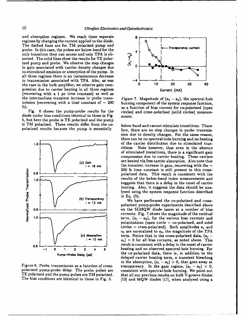
and absorption regimes. We reach these separate 8regimes by changing the current applied to the diode.The dashed lines are for TM polarized pump and I*---Transparency currentprobe. In this case, the pulses are below-band for the 4only transition they can access and only TPA is ob-served. The solid lines show the results for TE polar- iized pump and probe. We observe the step changesin gain associated with carrier density changes due 0to stimulated emission or absorption of the pump. Inall three regimes there is an instantaneous decreasein transmission associated with TPA. Also, as was -4the case in the bulk amplifier, we observe gain com- 0 10 20 30 40pression due to carrier heating in all three regimes Current (mA)(recovering with a 1 ps time constant) as well asthe intermediate transient increase in probe trans- Figure 7. Magnitude of (a, - a 2), the spectral-holemission (recovering with a time constant of - 200 burning component of the system response function,fs). as a function of bias current for co-polarized (open
Fig. 6 shows the pump-probe results for the circles) and cross-polarized (solid circles) measure-diode under bias conditions identical to those in Fig. ments.5, but here the probe is TE polarized and the pumpis TM polarized. These results differ from the co- below-band and cannot stimulate transitions. There-polarized results because the pump is essentially fore, there are no step changes in probe transmis-
sion due to density changes. For the same reason,there can be no spectral-hole burning and no heating
1.0- of the carrier distribution due to stimulated tran-sitions. Note however, that even in the absenceof stimulated transitions, there is a significant gaincompression due to carrier heating. These carriers
) Gare heated via free carrier absorption. Also note that1 1s rA the transient increase in gain, recovering with the -
05 200 fs time constant is still present in this cross-o"__._ _,_, , , , , polarized data. This result is consistent with the
E i.0- results of the below-band index measurements andsuggests that there is a delay in the onset of carrierheating. Also, it suggests the data should be ana-
* lyzed using the system response function describedne in Eq. (5).a. n We have performed the co-polarized and cross-
"o I -- 12 rA polarized pump-probe experiments described above0.9 , on the SLMQW diode lasers at a number of biasa currents. Fig. 7 shows the magnitude of the residual
o 1.0- term. (al - a2), for the various bias currents andZpolarizations (open circle = co-polarized, and solidcircles = cross-polarized). Both amplitudes a1 anda2 are normalized to a3 , the magnitude of the TPA
(c) Absorptiion term. Notice that in the cross-polarized data, (a, -I - 10 MA a2) ý- 0 for all bias currents, as noted above. This
0.9 __ ,_,_,_, _, result is consistent with a delay in the onset of carrier-1 0 1 2 3 4 5 heating and no observed spectral-hole burning. For
Pump-Probe Delay (ps) the co-polarized data, there is, in addition to thedelayed carrier heating term, a transient bleachingin the absorption, (a1 - a2) > 0, that goes away at
Figure 6. Probe transmission as a function of cross- transparency. In the gain regime, (a, - a2) < 0,polarized pump-probe delay. The probe pulses are consistent with spectral-hole burning. We point outTE polarized and the pump pulses are TM polarized, that all our previous results on bulk V-groove diodesThe bias conditons are identical to those in Fig. 5. (121 and MQW diodes 1171, when analyzed using a
Ultrafast Electronics and Optoelectronics 11
system response function that includes a delay in the 6. R. S. Tucker and I. P. Kaminow, "High-frequencyonset of carrier heating, also show a residual term characteristics of directly modulated InGaAsP ridgewhose time constant is rT = 100-200 fs, and whose waveguide and buried heterostructure lasers," J. Light-amplitude changes sign at the transparency point, wave Technol., LT-2, 385, (1984).
7. R. Olshansky, P. Hill, V. Lanzisera, and W.Conclusion Powazinik, "Frequency response of 1.3/um InGaAsP
high-speed semiconductor lasers," IEEE J. QuantumThrough a series of pump-probe measurements of Electron., 23, 1410, (1987).various waveguide structures in the AIGaAs andInGaAsP material systems, we have found that the 8. C. B. Su, J. Eom, C. H. Lange, C. B. Kim, R. B.carrier heating nonlinearity present in both the gain Lauer, W. C. Rideout, and J. S. LaCourse, "Char-and refractive index measurements has a delay in its acterization of the dynamics of semiconductor lasersonset. That is, it takes a finite amount of time for using optical modulation," IEEE J. Quantum Elec-the carriers to be heated. By quantifying this delay tron., 28, 118, (1992).in carrier heating, we have also been able to identify 9. Y. Lai, K. L. Hall, E. P. Ippen, and G. Eisenstein,evidence of dynamic spectral-hole burning. Both the "Short pulse gain saturation in InGaAsP diode laserAIGaAs and InGaAsP material systems exhibit very amplifiers," IEEE Photon. Technol. Lett., 2, 711,similar behaviors in this regard. Aside from differ- (1990).ences in the time constants of the processes, the ul-trafast gain and refractive index behavior of the two 10. R. S. Grant and W. Sibbett, "Observations ofmaterials are qualitatively the same. ultrafast nonlinear refraction in an InGaAsP optical
We thank Chris Cook of M.I.T. Lincoln Labora- amplifier," Appl. Phys. Lett. 58, 1119 (1991).tory for antireflection coating our diode lasers. Also,we thank Uzi Koren and Greg Raybon at AT&T Bell 11. M. P. Kesler and E. P. Ippen, "SubpicosecondLetabs for supplying th eg A R-coate aLMt ATidell gain dynamics in GaAIAs laser diodes," Appl. Phys.Labs for supplying the AR-coated SLMQW diodes. Lett. 51, 1765 (1987).K. L. Hall gratefully acknowledges the support of aJSEP Fellowship. This work was supported in part 12. K. L. Hall, J. Mark, E. P. Ippen, and G. Eisen-by the AFOSR under Contract No. F49620-91-C- stein, "Femtosecond gain dynamics in InGaAsP op-0091, by the Joint Services Electronics Program un- tical amplifiers," Appl. Phys. Lett. 56, 1740 (1990).der Contract No. DAAL03-92-C-0001, by DARPA 13. P. J. Delfyett, Y. Silberberg, and G. A. Alphonse,through the National Center for Integrated Photon- "Hot-carrier thermalization induced self-phase mod-ics Technology, and by the NSF under Grant No. ulation in semiconductor traveling wave amplifiers,"
Appl. Phys. Lett. 59, 10 (1991).
References 14. C. T. Hultgren and E. P. Ippen, "Ultrafast re-fractive index dynamics in AIGaAs diode laser am-
1. L. F. Teimeijer, "Effects of nonlinear gain on four- plifiers," Appl. Phys. Lett. 59, 635 (1991).wave mixing and asymmetric gain saturation in a 15. K. L. Hall, G. Lenz, E. P. Ippen, and G. Ray-semiconductor laser amplifier," App1. Phys. Lett. bon, "Heterodyne pump-probe technique for time-59, 499 (1991). domain studies of optical nonlinearities in waveg-
2. S. R. Chinn, "Measurement of nonlinear gain uides," Opt. Lett., 17, 874, (1992).suppression and four-wave mixing in quantum well 16. C. T. Hultgren, D. J. Dougherty, and E. P. Ip-lasers," Appl. Phys. Lett., 59, 1673, (1991). pen, "Above- and below-band femtosecond nonlin-
3. R. Frankenberger and R. Schimpe, "Origin of earities in active AIGaAs waveguides," Appl. Phys.nonlinear gain saturation in index-guided InGaAsP Lett., 61, 2767, (1992).laser diodes," Appl. Phys. Lett. 60, 2720 (1992). 17. K. L. Hall, Y. Lai, E. P. Ippen, G. Eisenstein,4. K. Kikuchi, M. Kakui, C.-E. Zah, and T.-P. Lee, and U. Koren, "Femtosecond gain dynamics and sat-"Observation of highly nondegenerate four-wave mix- uration behavior in InGaAsP multiple quantum welling in 1.5 um traveling-wave semiconductor optical optical amplifiers," Appl. Phys. Lett., 57, 2888,amplifiers and estimation of nonlinear gain coeffi- (1990).cient," IEEE J. Quantum Electron. 28, 151 (1992). 18. K. L. Hall, G. Lenz, E. P. Ippen, U. Koren, and
5. R. Nietzke, P. Panknin, W. Elsisser, and E. O. G. Raybon, "Carrier heating and spectral-hole burn-G~bel, "Four-wave mixing in GaAs/AIGaAs Semi- ing in strained-layer quantum-well laser amplifiers atconductor Lasers," IEEE J. Quantum Electron. 25, 1.5 um," Appl. Phys. Lett., 61, 2512, (1992).1399 (1989).
12 Ultrafast Electronics and Optoelectronics
19. M. J. LaGasse, K. K. Anderson, H. A. Haus, and 21. G. Bastard, Wave Mechanics Applied to
3. G. Fujimoto, "Femntosecond all-optical switching Semiconductor Heterostructures, (Halsted, New York,in AlGaAs waveguides using a time division inter- 1988).ferometer," Appl. Phys. Lett. 54, 2068 (1989). 22. 3. Mark, L. Y. Liu, K. L. Hall, H. A. Haus,
20. U. Koren, M. Oron, M. G. Young, B. I. Miller, and E. P. Ippen, "Femtosecond pulse generation inJ. L. De Miguel, G. Raybon, and M. Chien, "Low a laser with a nonlinear external resonator," Opt.threshold highly efficient strained quantum well lasers Lett., 14, 48, (1989).at 1.5 micrometre wavelength," Electron. Lett., 26,465, (1990).
Carrier Transport Effects in High Speed Quantum WellLasers
Radlakrishnan Nagarajan
Department of Electrical and Computer Engineering, University of California,Santa Barbara, California 93106
Abstract well lasers. This leads to enhanced frequency
modulation response and increased wavelength chirping
The high speed properties of quantum well lasers, like under intensity modulation in quantum well lasers with
the amplitude modulation (AM) and frequency dominant carrier transport effects [12,14,15].
modulation (FM) response, and wavelength chirping aresignificantly affected by the carrier transport across the Carrier Transport Modeloptical and current confining layers, and thermionicemission out of the quantum well active area. Fig. 1 shows a SCH single quantum well (SQW). We
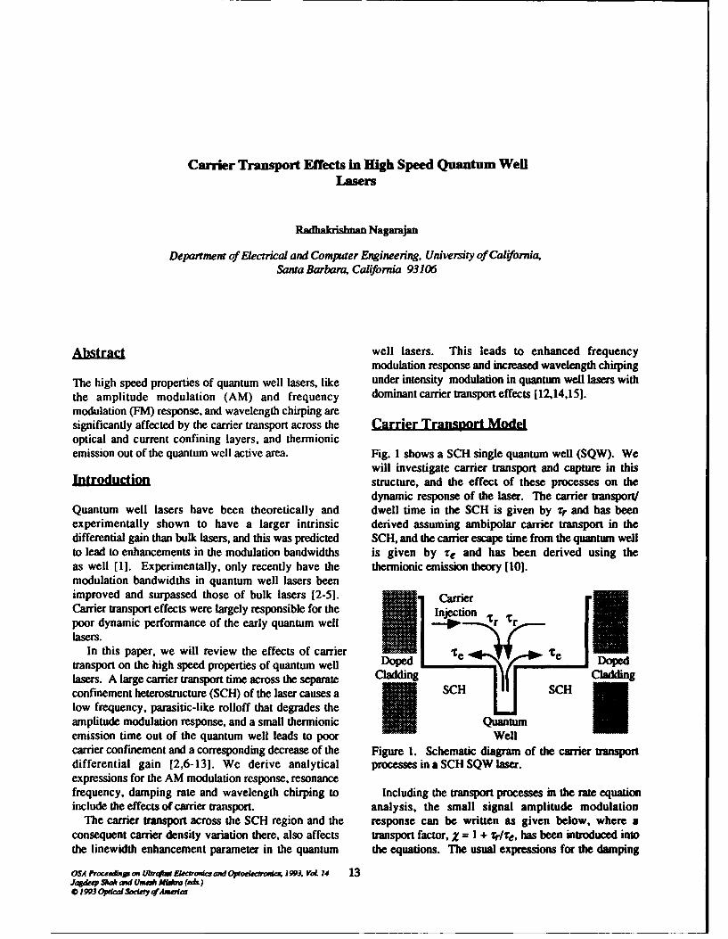
will investigate carrier transport and capture in thisSistructure, and the effect of these processes on the
dynamic response of the laser. The carrier transport/Quantum well lasers have been theoretically and dwell time in the SCH is given by rr and has beenexperimentally shown to have a larger intrinsic derived assuming ambipolar carrier transport in thedifferential gain than bulk lasers, and this was predicted SCH, and the carrier escape time from the quantum wellto lead to enhancements in the modulation bandwidths is given by re and has been derived using theas well [1). Experimentally, only recently have the thermionic emission theory [10].modulation bandwidths in quantum well lasers beenimproved and surpassed those of bulk lasers [2-5]. CarrierCarrier transport effects were largely responsible for the Injectionpoor dynamic performance of the early quantum well 'r-- rlasers.
In this paper, we will review the effects of carrier ie Tetransport on the high speed properties of quantum well Doped
lasers. A large carrier transport time across the separate Cladding Cldi gconfinement heterostructure (SCH) of the laser causes a SCH SCHlow frequency, parasitic-like rolloff that degrades theamplitude modulation response, and a small thermionic Quantumemission time out of the quantum well leads to poor Wellcarrier confinement and a corresponding decrease of the Figure 1. Schematic diagram of the carrier transportdifferential gain [2,6-13]. We derive analytical processes in a SCH SQW laser.expressions for the AM modulation response, resonancefrequency, damping rate and wavelength chirping to Including the transport processes in the rate equationinclude the effects of carrier transport. analysis, the small signal amplitude modulation
The carrier transport across the SCH region and the response can be written as given below, where aconsequent carrier density variation there, also affects transport factor, X = 1 + ?r/re, has been introduced intothe linewidth enhancement parameter in the quantum the equations. The usual expressions for the damping
oSA Pro•aeng, on Uhfrqw ElH rci, md Oproerkmwrcu 1993, VoL 14 13JagEdm a md Ue Miqwu (e&)0 1W3 Opidca1 & qqfAnMe
14 Ultrafast Electronics and Optoelectronics
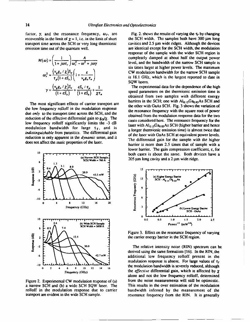
factor, y, and the resonance frequency, Wr, are Fig. 2. shows the results of varying the Tr by changingrecoverable in the limit of x = 1, i.e. in the limit of short the SCH width. The samples both have 300 ;.tm longtransport time across the SCH or very long thermionic cavities and 2.5 pm wide ridges. Although the devicesemission time out of the quantum well. are identical except for the SCH width, the modulation
response of the sample with the wider SCH region isI A completely damped at about half the output power
(2 _2 level, and the bandwidth of the narrow SCH sample issix times larger at higher power levels. The maximum
2= (Vgo/x)So r1+ e CW modulation bandwidth for the narrow SCH samplew,= -p 0-'
0o. vg Jr. is 18.1 GHz, which is the largest reported to date inSQW lasers.
(vgo /x) 0S+ eS. I ", 1 The experimental data for the dependence of the high
(I+ eS.) (+ l+eSo) + -Z, speed parameters on the thermionic emission time isobtained from two samples with different energybarriers in the SCH; one with Al0 .15Gao 35As SCH and
The most significant effects of carrier transport are the other with GaAs SCH ano
the low frequency rolloff in the modulation response the other with the varoo n of
due only to the transport time across the SCH, and the the resonance frequency with the square root of power
reduction of the effective differential gain to go/z. The obtained from the modulation response data for the two
low frequency rolloff significantly limits the -3 dB cases considered here. The resonance frequency for the
modulation bandwidth for large r~ r, and is laser with Alo.15Gao.g5As SCH (higher barrier and hencea longer thermionic emission time) is almost twice thatindistinguishable from parasitics. The differential gain of the laser with GaAs SCH at equivalent power levels.
reduction is only apparent in the dynamic sense, and it the daferenti Gain for theqsale w e her
does not affect the static properties of the laser. The differential gain for the sample with the higherbarrier is more than 2.5 times that of sample with a
lower barrier. The gain compression coefficient, E, for10.o both cases is about the same. Both devices have a
6 205 gam long cavity and a 2 gm wide ridge.
S3.1 8.0t• 15
V 20.943.3 m" (a) Higher Energy Barrier$.2 12"H-AýS%8A
59-6
-1060 4 12 16 20
Frequency (GHz) z 3 ( Lower Enegy Baia04~50 S;t- G!As
0 .at .a' l t l l ' ' I
10 if 0.0 0.5 1.0 1.5 2.0 2.52.4 (b) Wide SCH Sfi2le Power"r (mW")
6 0.9 7.4 scHwPower' ")
R Figure 3. Effect on the resonance frequency of varyingSO 2 13.4 the carrier energy barrier in the SCH region.
-2 30.0 The relative intensity noise (RIN) spectrum can be
derived using the same formalism [16]. In the RIN, the-6 42.7mW additional low frequency rolloff present in the
modulation response is absent. For large values of •r
0 2 4 6 o 10 12 14 16 the modulation bandwidth is severely reduced, althoughFrequency (GHz) the effective differential gain, which is affected by Z
alone and not the low frequency rolloff, determinedFigure 2. Experimental CW modulation response of (a) from the noise measurements will still be optimistic.a narrow SCH and (b) a wide SCH SQW laser. The This results in the over estimation of the modulationrolloff in the modulation response due to carrier bandwidth inferred by the measurement of thetransport are evident in the wide SCH sample. resonance frequency from the RIN. It is generally
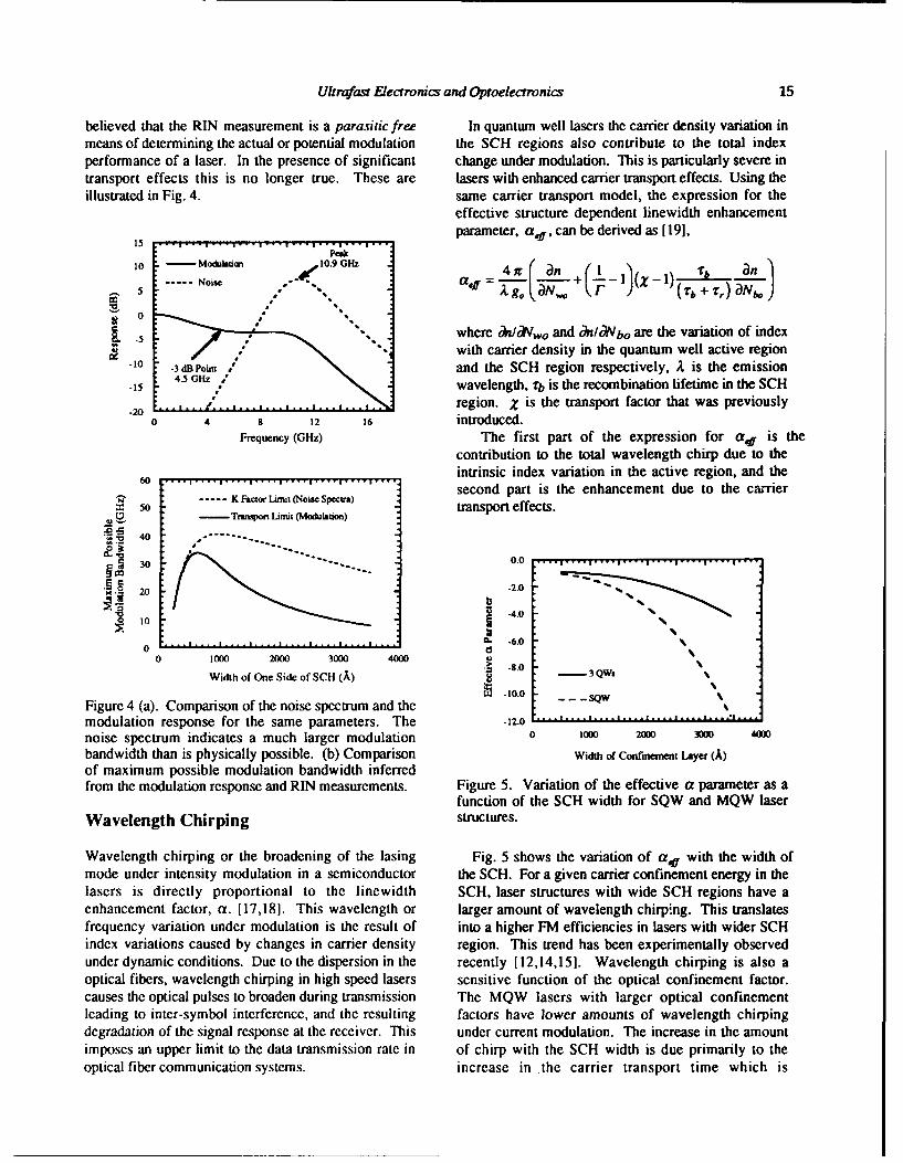
Ultrafast Electronics and Optoelectronics 15
believed that the RIN measurement is a parasitic free In quantum well lasers the carrier density variation inmeans of determining the actual or potential modulation the SCH regions also contribute to the total indexperformance of a laser. In the presence of significant change under modulation. This is particularly severe intransport effects this is no longer true. These are lasers with enhanced carrier transport effects. Using theillustrated in Fig. 4. same carrier transport model, the expression for the
effective structure dependent linewidth enhancement15 _. _. _. _._ ._ ._ ._ ..._parameter, aff , can be derived as [191,15 ..
4.. . ., .
r---an-- -, -
Peak
NoseI I (.,-_1)- -- _L_,, ,b+ +T,)aN
-5 where dnI/aVo and nldNbo are the variation of index
-10 with carrier density in the quantum well active region-40 dB and the SCH region respectively, A is the emission
-15 4 .53G t.,"1 wavelength, rb is the recombination lifetime in the SCHregion. Z is the transport factor that was previously
-20
t ... ..
0 4 8 12 16 introduced.Frequency (GHz) The first part of the expression for af is the
contribution to the total wavelength chirp due to the
intrinsic index variation in the active region, and theK0 .... Limi (Noise S t ........ .. second part is the enhancement due to the carrier
s" o
transport effects."• .. .K Factor Lim it (N oise Sp~ectra) t a s o t e f c sTranmspor Limit (Modulation)
.es40
• 30
0.0..... .... .... ......... ..... ..... ......-2.0 =
30
.1
IS202.
010 010030 2000 3000 4000
• -.
Width of One Side of SCH (A) 3Qwi
Figure 4 (a). Comparison of the noise spectrum and the - -sQw %modulation response for the same parameters. The -12.0noise spectrum indicates a much larger modulation 0 1000 2000 3 4
b a n d w id th tha n is p h y sica lly p o ssib le . (b ) C o m p ariso n W idt of Confinem ent Layer (A )of maximum possible modulation bandwidth inferredfrom the modulation response and RIN measurements. Figure 5. Variation of the effective a parameter as a
function of the SCH width for SQW and MQW laserWavelength Chirping structures.
Wavelength chirping or the broadening of the lasing Fig. 5 shows the variation of as with the width ofmode under intensity modulation in a semiconductor the SCH. For a given carrier confinement energy in thelasers is directly proportional to the linewidth SCH, laser structures with wide SCH regions have aenhancement factor, a. [17,181. This wavelength or larger amount of wavelength chirping. This translatesfrequency variation under modulation is the result of into a higher FM efficiencies in lasers with wider SCHindex variations caused by changes in carrier density region. This trend has been experimentally observedunder dynamic conditions. Due to the dispersion in the recently [12,14,15]. Wavelength chirping is also aoptical fibers, wavelength chirping in high speed lasers sensitive function of the optical confinement factor.causes the optical pulses to broaden during transmission The MQW lasers with larger optical confinementleading to inter-symbol interference, and the resulting factors have lower amounts of wavelength chirpingdegradation of the signal response at the receiver. This under current modulation. The increase in the amountimposes an upper limit to the data transmission rate in of chirp with the SCH width is due primarily to theoptical fiber communication systems. increase in the carrier transport time which is
16 Ultrafast Eectrnics and Optoelectronimc
proportional to the square of the SCH width, and the 8. R. Nagarajan, T. Fukushima, M. Ishikawa, J. E.decrease in the optical confinement factor. Bowers, R. S. Geels, and L. A. Coldren,
"Transport Limits in High Speed Quantum WellLasers: Experiment and Theory," Photon. Tech.Lett. 4, 121 (1992).
9. T. C. Wu, S. C. Kan, D. Vassilovski, K. Y. Lau,C. E. Zah, B. Pathak, and T. P. Lee, "Gain
In summary, the carrier transport has a significant Compression in Tensile-Strained 1.55 tumeffect on the high speed properties of quantum well Quantum Well Lasers Operating at First andlasers. Careful device design is required to take Second Quantized Levels," Appl. Phys. Lett. 0,advantage of the enhancement in differential gain 1794 (1992).obtained by the use of quantum wells in the active area. 10. R. Nagarajan, M. Ishikawa, T. Fukushima, R. S.A mere replacement of the active area in a bulk laser by Geels and J. E. Bowers, "High Speed Quantumquantum wells is not sufficient. Well Lasers and Carrier Transport Effects," IEEE
J. Quantum Electron. 2& 1990 (1992).11. N. Tessler, R. Nagar, and G. Eisentsein,
Acknowledgments "Structure Dependent Modulation Responses inQuantum-Well Lasers," IEEE J. Quantum
This work was funded by DARPA, Rome Laboratories Electron. 2L 2242(1992).
(Hanscom AFB) and Office of Naval Technology block 12. A. P. Wright, B. Garrett, G. H. B. Thompson, andp. E. A. Whiteaway, "Influence of Carrierprogram in Electro-Optics Technology. Transport on Wavelength Chirp of InGaAs/
InGaAsP MQW Lasers," Electron. LetL, 28,1911, (1992).
R rces 13. B. Zhao, T. R. Chen, Y. Yamada, Y. H. Zhuang,N. Kuze, and A. Yariv, "Evidence for State
1. I. Suemune, "Theoretical Study of Differential Filling Effect on High Speed ModulationGain in Strained Quantum Well Structures," Dynamics of Quantum Well Lasers," Appl. Phys.IEEE J. Quantum Electron. 2J, 1149 (1991). Lett. a, 1907 (1992).
2. R. Nagarajan, R. P. Mirin, T. E. Reynolds, and J. 14. I. H. White, P. S. Griffin, K. A. Williams, G. H.E. Bowers, "Effect of the Confinement Layer B. Thompson, J. E. A. Whiteaway, and B.Composition on the Internal Quantum Efficiency Garrett, "Spectral Dynamics of Long Wavelengthand Modulation Response of Quantum Well Quantum Well Distributed Feedback DiodeLasers," IEEE Photon. Tech. Lett. 4, 832 (1992). Lasers under Gain Switching," in Tehnical
3. R. Nagarajan, T. Fukushima, J. E. Bowers, R. S. Digest of 13th IEEE International SemiconductorGeels, and L. A. Coldren, "High-Speed LeQ fere= (1992), pp. 264.InGaAs/GaAs Strained Multiple Quantum Well 15. H. Yamazaki, M. Yamaguchi, M. Kitamura, andLasers with Low Damping," Appl. Phys. Lett. 2, I. Mito, "Analysis of FM Efficiency of2326(1991). InGaAs/InGaAsP SCH-MWQ LDs Taking
4. L. F. Lester, S. S. O'Keefe, W. J. Schaff, and L. Injection Carrier Transport into Account," inF. Eastman, "Multiquantum Well Strained-Layer Technical Digest of 13th IEEE InternationalLasers with Improved Low Frequency Response Semiconductor Laser Conference(1992), pp. 174.and Very Low Damping," Electron. Lett. 2a, 383 16. R. Nagarajan, M. Ishikawa, and J. E. Bowers,(1992). "Effects of Carrier Transport on Relative
5. S. Weisser, J. D. Ralston, E. C. Larkins, I. Intensity Noise and Critique of K FactorEsquivias, P. J. Tasker, J. Fieissner, and J. Prediction of Modulation Response," Electron.Rosenzweig, "Efficient High-Speed Direct Lett. M, 846 (1992).Modulation in p-Doped In0.35Ga 0.65As/GaAs 17. T. L. Koch, and J. E. Bowers "Nature ofMultiquantum Well Lasers," Electron. Lett. 2&, Wavelength Chirping in Directly Modulated2141 (1992). Semiconductor Lasers," Electron. Lett. 2Q, 1038
6. W. Rideout, W. F. Sharfin, E. S. Koteles, M. 0. (1984).Vassell, and B. Elman, "Well-Barrier Hole 18. C. H. Henry, "Theory of Linewidth ofBurning in Quantum Well Lasers," IEEE Photon. Semiconductor Lasers," IEEE J. QuantumTech. LetL 1, 784 (1991). Electron. a, 259 (1982).
7. R. Nagarajan, T. Fukushima, S. W. Corzine, and 19. R. Nagarajan, and J. E. Bowers, "Effects ofJ. E. Bowers, "Effects of Carrier Transport on Carrier Transport on Injection Efficiency andHigh-Speed Quantum Well Lasers," Appl. Phys. Wavelength Chirping in Quantum Well Lasers,"Lett. 59, 1835 (1991). IEEE J. Quantum Electron., June 1993.
8.6-GHz Active, Passive, and Hybrid Mode-Locking ofInGaAsP Extended-Cavity MQW Lasers with Monolithically
Integrated Saturable Absorbers
P. B. Hansen, G. Raybon, U. Koren, B. I. Miller, M. G. Young, M. A. Newkirk, andC. A. Burrus
A T& T Bell Laboratories, Crawford Hill Laboratory, Holmdel, New Jersey 07733
P. P. lannone
Princeton University, Department of Electrical Engineering, Princeton, New Jersey 08544
Abstract Passive and hybrid mode-locking of long-wavelengthall-active semiconductor lasers have been reported
Active, passive, and hybrid mode-locking have been yielding sub-picosecond pulse widths and repetitiondemonstrated in a monolithic extended-cavity rates in the 40 GHz to 350 GHz range 151. In thesemiconductor laser with an integrated saturable GaAIAs system, active, passive and hybrid mode-absorber. A 45-ýtm long reverse-biased segment of locking of all-active waveguide lasers have beenmultiple quantum wells acts as the saturable absorber. demonstrated at repetition rates down to 5.5 GHz [6].Active and hybrid mode-locking at a repetition rate of In this letter, we report an InGaAsP monolithic8.6 GHz, resulted in 6.2-ps and 4.4-ps pulses. The extended-cavity laser with an integrated passiveextended-cavity laser also exhibits self-starting passive waveguide and a saturable absorber. This laser devicemode-locking at a repetition rate of 8.57 GHz with 5.5 allows active, passive, as well as hybrid mode-lockingps pulses. Wavelength selectivity over a range of 15 at a repetition rate of 8.6 GHz. The mode-lockingnm with little change in the pulse width is facilitated method is given by the applied biasing scheme. Pulsesby a broad spectrum, with durations of 4-5 ps are obtained by passive and
hybrid mode-locking, whereas active mode-lockingyields 6-9 ps pulses. A broad spectrum allows
Introduction wavelength selectivity over a range of 15 nm with littlechange in the pulse profile by means of external
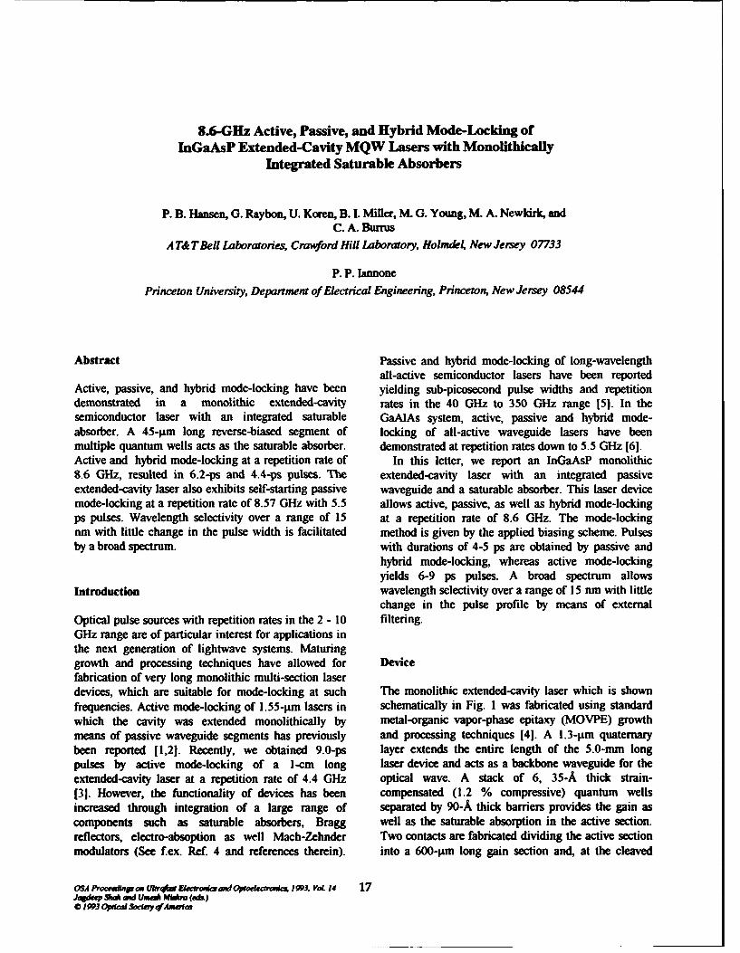
Optical pulse sources with repetition rates in the 2 - 10 filtering.GHz range are of particular interest for applications inthe next generation of lightwave systems. Maturinggrowth and processing techniques have allowed for Devicefabrication of very long monolithic multi-section laserdevices, which are suitable for mode-locking at such The monolithic extended-cavity laser which is shownfrequencies. Active mode-locking of 1.55-pIm lasers in schematically in Fig. 1 was fabricated using standardwhich the cavity was extended monolithically by metal-organic vapor-phase epitaxy (MOVPE) growthmeans of passive waveguide segments has previously and processing techniques [4]. A 1.3-tun quaternarybeen reported [1,2]. Recently, we obtained 9.0-ps layer extends the entire length of the 5.0-mm longpulses by active mode-locking of a 1-cm long laser device and acts as a backbone waveguide for theextended-cavity laser at a repetition rate of 4.4 GHz optical wave. A stack of 6, 35-A thick strain-[3]. However, the functionality of devices has been compensated (1.2 % compressive) quantum wellsincreased through integration of a large range of separated by 90-A thick barriers provides the gain ascomponents such as saturable absorbers, Bragg well as the saturable absorption in the active section.reflectors, electro-absoption as well Mach-Zehnder Two contacts are fabricated dividing the active sectionmodulators (See f.ex. Ref. 4 and references therein), into a 600-jtm long gain section and, at the cleaved
OS P'oced~ on Ubkrw o N ti aO,$oefr•cveim ,•993, VoL 14 17Jagdeep Shah and UnwA Mitka (e&)0 1993 Optca Society #*'Amwknl
18 Ultrafast Electronics and Optoelectronics
Sat. Gain section Passive waveguide 100abs. (a)
SSCI. MQW1.3-pm quaternaxy
InP substrate
45 30rn~im •50 .
Figure 1. Schematic drawing of the monolithic 6
extended-cavity laser with an integrated saturableabsorber. SCL: Strain-compensated layers. MQW:Multiple quantum wells. SI: Semi-insulating.
facet, a 45-jin long saturable absorber. The resistancebetween the gain and absorber contacts, which are 0separated by a 30-gim wide etched groove through the 0 45 90 135 180
p+-InGaAs contacting layer, is 1.5 kI. The active 100segment is a buried heterostructure with semi- (b)insulating (SI) InP regrown for current blocking. Thelaser cavity has been monolithically extended byincorporating a 4.3-mm long passive waveguide. Aburied rib waveguide structure with the SI-InP actingas the cladding layer results in losses of 4-5 dB/cmrwhich allows integration of a long passive waveguide 50 4 .4 pswhile maintaining a threshold current of only 50 mA
(40 mA and 10 mA applied to the gain and absorbersections, respectively).
Mode-locking0 -
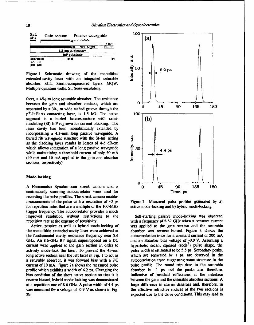
A Hamamatsu Synchro-scan streak camera and a 0 45 90 135 180continuously scanning autocorrelator were used for Time, psrecording the pulse profiles. The streak camera enablesmeasurements of the pulse with a resolution of -3 ps Figure 2. Measured pulse profiles generated by a)for repetition rates that are a multiple of the 100-MHz active mode-locking and b) hybrid mode-locking.trigger frequency. The autocorrelator provides a muchimproved resolution without restrictions to the Self-starting passive mode-locking was observedrepetition rate at the expense of sensitivity, with a frequency of 8.57 GHz when a constant current
Active, passive as well as hybrid mode-locking of was applied to the gain section and the saturablethe monolithic extended-cavity laser were achieved at absorber was reverse biased. Figure 3 shows thethe fundamental cavity resonance frequency near 8.6 autocorrelation trace for a constant current of 200 mAGHz. An 8.6-GHz RF signal superimposed on a DC and an absorber bias voltage of -0.9 V. Assuming acurrent were applied to the gain section in order to hyperbolic secant squared (sech2 ) pulse shape, theactively mode-lock the laser. To prevent the 45-jim pulse width is estimated to be 5.5 ps. Secondary peaks,long active section near the left facet in Fig. 1 to act as which are separated by 1 ps, are observed in thea saturable absort.-r, it was forward bias with a DC autocorrelation trace suggesting some structure in thecurrent of 10 mA. Figure 2a shows the measured pulse pulse profile. The round trip time in the saturableprofile which exhibits a width of 6.2 ps. Changing the absorber is -1 ps and the peaks are, therefore,bias condition of the short active section so that it is indicative of residual reflections at the interfacereverse biased, hybrid mode-locking was demonstrated between the gain and the saturable absorber sections. Aat a repetition rate of 8.6 GHz. A pulse width of 4.4-ps large difference in carrier densities and, therefore, inwas measured for a voltage of -0.9 V as shown in Fig. the effective refractive indices of the two sections is2b. expected due to the drive conditions. This may lead to
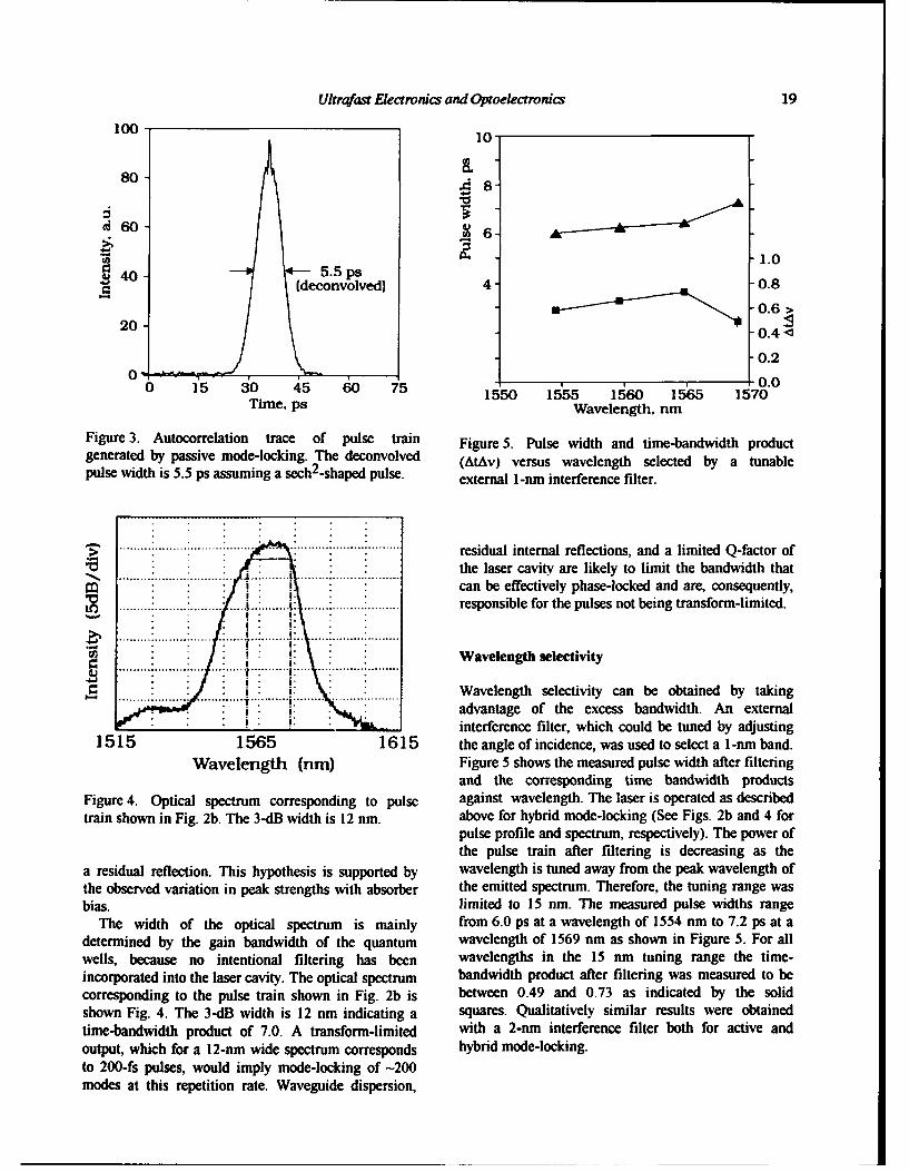
Ultrafast Electronics and Oproelectronics 19
100 10
80
1.040- 5.5 ps
(deconvolved) 4- 0.8- M__"0.6 >
20- 0.6-0.44
-0.2O'%0 15* 5i0.00 15 30 5 6 7 1550 15'55 1560 1565 1570
Time, ps Wavelength. nm
Figure 3. Autocorrelation trace of pulse train Figure 5. Pulse width and time-bandwidth productgenerated by passive mode-locking. The deconvolved (AtAv) versus wavelength selected by a tunablepulse width is 5.5 ps assuming a sech 2 -shaped pulse. external l-nm interference filter.
. residual internal reflections, and a limited Q-factor ofthe laser cavity are likely to limit the bandwidth that
S.can be effectively phase-locked and are, consequently,. responsible for the pulses not being transform-limited.
Wavelength selectivity
. Wavelength selectivity can be obtained by takingadvantage of the excess bandwidth. An externalinterference filter, which could be tuned by adjusting
1515 1565 1615 the angle of incidence, was used to select a 1-nm band.
Wavelength (nm) Figure 5 shows the measured pulse width after filteringand the corresponding time bandwidth products
Figure 4. Optical spectrum corresponding to pulse against wavelength. The laser is operated as describedtrain shown in Fig. 2b. The 3-dB width is 12 nm. above for hybrid mode-locking (See Figs. 2b and 4 for
pulse profile and spectrum, respectively). The power ofthe pulse train after filtering is decreasing as the
a residual reflection. This hypothesis is supported by wavelength is tuned away from the peak wavelength ofthe observed variation in peak strengths with absorber the emitted spectrum. Therefore, the tuning range wasbias. limited to 15 nm. The measured pulse widths range
The width of the optical spectrum is mainly from 6.0 ps at a wavelength of 1554 nm to 7.2 ps at adetermined by the gain bandwidth of the quantum wavelength of 1569 nm as shown in Figure 5. For allwells, because no intentional filtering has been wavelengths in the 15 nm tuning range the time-incorporated into the laser cavity. The optical spectrum bandwidth product after filtering was measured to becorresponding to the pulse train shown in Fig. 2b is between 0.49 and 0.73 as indicated by the solidshown Fig. 4. The 3-dB width is 12 nm indicating a squares. Qualitatively similar results were obtainedtime-bandwidth product of 7.0. A transform-limited with a 2-nm interference filter both for active andoutput, which for a 12-nm wide spectrum corresponds hybrid mode-locking.to 200-fs pulses, would imply mode-locking of -200modes at this repetition rate. Waveguide dispersion,
20 Utrafast Electronics and Optoelectronics
Conclusion References:
In conclusion, active, passive as well as hybrid mode- 1. R. S. Tucker, U. Koren, G. Raybon, C. A. Burrus,locking of a monolithic extended-cavity laser with an B. I. Miller, T. L. Koch, and G. Eisenstein, "40integrated saturable absorber are demonstrated. The GHz active mode-locking in a 1.5 mm monolithicsaturable absorber is obtained by reverse biasing a 45- extended-cavity laser", Elec. Lett., 25, 621-622pam long section of MWQs. This section is forward (1989).biased during active mode-locking. All three mode- 2. P. B. Hansen, G. Raybon, U. Koren, B. I. Miller,locking schemes are seen to provide short optical M. G. Young, M. -D. Chien, C. A. Burrus, and R.pulses at 8.6 GHz, which corresponds to the C. Alferness, "5.5-mm Long InGaAsP monolithicfundamental cavity resonance frequency of the 5.0-mm extended-cavity laser with an integrated Bragglong device. Passive and hybrid mode-locking typically reflector for active mode-locking", Photon. Techn.yields shorter pulse durations than active mode- Lett., 4, 215-217 (1992).locking. Hybrid mode-locking results in the shortest 3. G. Raybon, P. B. Hansen, U. Koren, B. I. Miller,pulses, i.e. 4.4 ps, and, furthermore, offers the M. G. Young, M. Newkirk, P. P. lanonne, C. A.convenience of active mode-locking in terms of Burrus, J. Centanni, and M. Zirngibl, "Activegenerating a pulse train phase-locked to the applied mode-locking at 4.4 GHz in a 1-cm longelectrical drive signal. A 12-nm wide spectrum aliowed monolithic extended-cavity laser", Techincalwavelength selection by tuning an external 1-nm Digest of LEOS'92 Annual Meeting (Opticalinterference filter. Pulse durations between 6.0 ps and Society of America, Washington, DC, 1992),7.2 ps were obtained over a tuning range of 15 nm. Paper DLTA4.3.The corresponding time-bandwidth products ranged 4. T. L. Koch and U. Koren, "Semiconductorfrom 0.49 to 0.73. photonic integrated circuits", IEEE J. Quantum
Electron., 27, 641-653 (1991).5. Y. K. Chen, M. C. Wu, T. Tanbun-Ek, R. A.
Logan, and M. A. Chin, "Subpicosecondmonolithic colliding-pulse mode-locked multiplequantum well lasers", Appl. Phys. Lett., 58, 1253-1255 (1991).
Acknowledgments 6. D. J. Derickson, P. A. Morton, and J. E. Bowers,"Comparison of timing jitter in external and
The authors would like to acknowledge N. Frigo and monolithic cavity mode-locked semiconductorE. Ippen for a number of helpful discussions. laser", Appl. Phys. Lett., 59, 3372-3374 (1991).
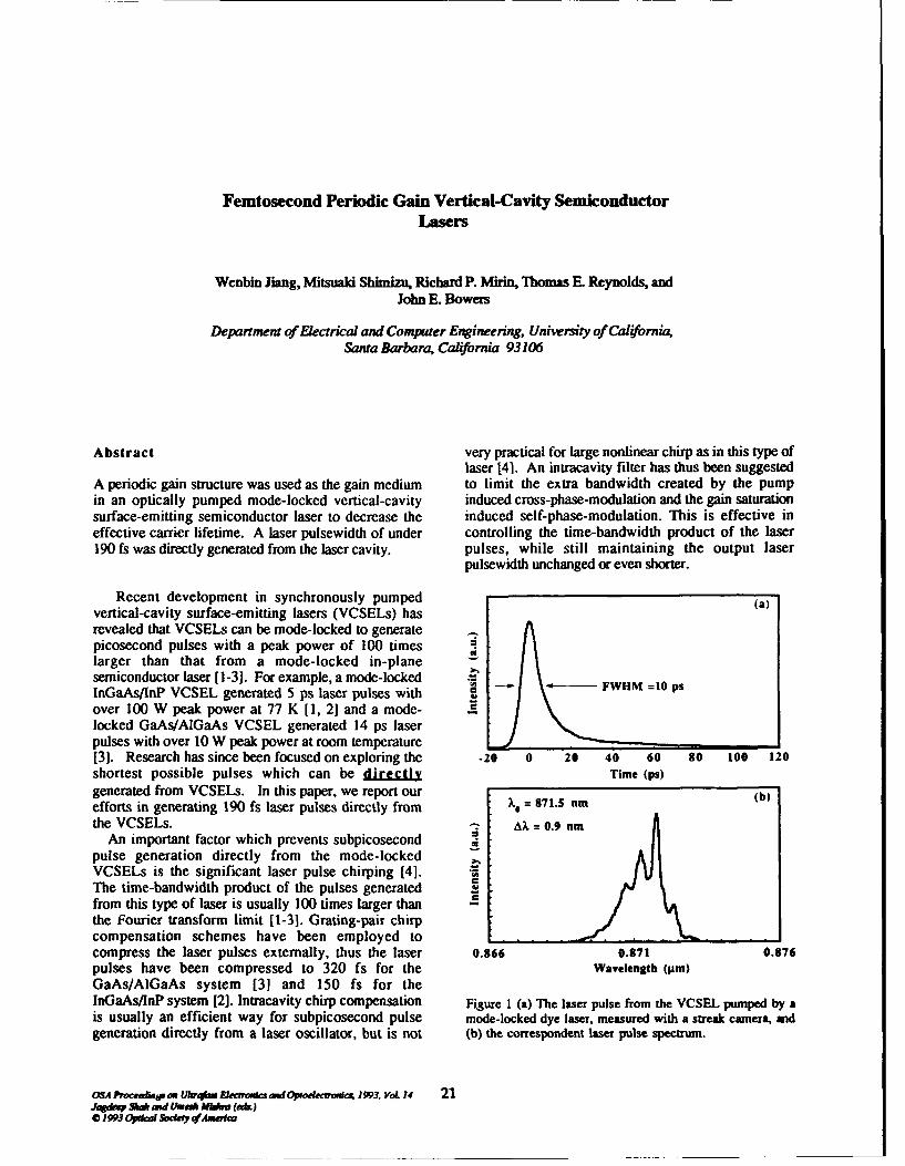
Femtosecond Periodic Gain Vertical-Cavity SemiconductorLasers
Wenbin Jiang, Mitsuaki Shimizu, Richard P. Mirin, Thomas E. Reynolds, andJohn E. Bowers
Department of Electrical and Computer Engineering, University of California,Santa Barbara, California 93106
Abstract very practical for large nonlinear chirp as in this type oflaser 14]. An intracavity filter has thus been suggested
A periodic gain structure was used as the gain medium to limit the extra bandwidth created by the pumpin an optically pumped mode-locked vertical-cavity induced cross-phase-modulation and the gain saturationsurface-emitting semiconductor laser to decrease the induced self-phase-modulation. This is effective ineffective carrier lifetime. A laser pulsewidth of under controlling the time-bandwidth product of the laser190 fs was directly generated from the laser cavity, pulses, while still maintaining the output laser
pulsewidth unchanged or even shorter.
Recent development in synchronously pumped (a)vertical-cavity surface-emitting lasers (VCSELs) hasrevealed that VCSELs can be mode-locked to generatepicosecond pulses with a peak power of 100 timeslarger than that from a mode-locked in-planesemiconductor laser [1-3]. For example, a mode-lockedInGaAs/InP VCSEL generated 5 ps laser pulses with W
over 100 W peak power at 77 K [1, 2] and a mode- .9locked GaAs/AIGaAs VCSEL generated 14 ps laserpulses with over 10 W peak power at room temperature[3]. Research has since been focused on exploring the -20 0 20 40 60 SO 100 120
shortest possible pulses which can be diJgc.ily Time (ps)
generated from VCSELs. In this paper, we report our (b)efforts in generating 190 fs laser pulses directly from ke = 871.5 nm
the VCSELs. AX =0.9 m rAn important factor which prevents subpicosecond
pulse generation directly from the mode-lockedVCSELs is the significant laser pulse chirping [4].The time-bandwidth product of the pulses generatedfrom this type of laser is usually 100 times larger than -the Fourier transform limit [1-31. Grating-pair chirpcompensation schemes have been employed tocompress the laser pulses externally, thus the laser 0.866 0.371 0.876pulses have been compressed to 320 fs for the Wavelength (prm)GaAs/AIGaAs system [3] and 150 fs for theInGaAs/InP system [2]. Intracavity chirp compensation Figure 1 (a) The laser pulse from the VCSEL pumped by ais usually an efficient way for subpicosecond pulse mode-locked dye laser, measured with a streak camera, andgeneration directly from a laser oscillator, but is not (b) the correspondent laser pulse spectrum.
OSA PAoczdv on UkrMm BK mooekecnlcsý 1993, VoL 14 21Jqgdaq 56 amd Vu.M *iWmi (ak)0 1993 Opdcal Socgery fAmerim
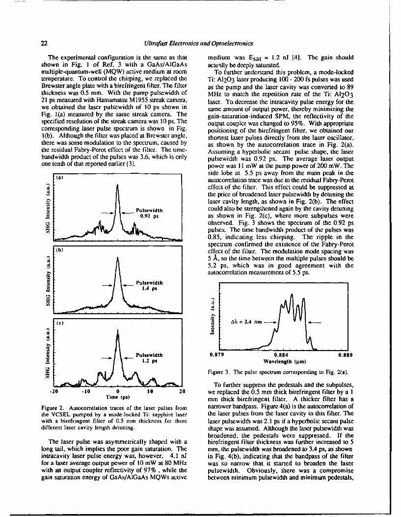
22 Ultrafost Electronics and Optoelectronics
The experimental configuration is the same as that medium was Esat = 1.2 nJ [4]. The gain shouldshown in Fig. I of Ref. 3 with a GaAs/AIGaAs actually be deeply saturated.multiple-quantum-well (MQW) active medium at room To further understand this problem, a mode-lockedtemperature. To control the chirping, we replaced the Ti: A1203 laser producing 100 - 200 fs pulses was usedBrewster angle plate with a birefringent filter. The filter as the pump and the laser cavity was converted to 89thickness was 0.5 mm. With the pump pulsewidth of MHz to match the repetition rate of the Ti: A120321 ps measured with Hamamatsu M1955 streak camera, laser. To decrease the intracavity pulse energy for thewe obtained the laser pulsewidth of 10 ps shown in same amount of output power, thereby minimizing theFig. 1(a) measured by the same streak camera. The gain-saturation-induced SPM, the reflectivity of thespecified resolution of the streak camera was 10 ps. The output coupler was changed to 95%. With appropriatecorresponding laser pulse spectrum is shown in Fig. positioning of the birefringent filter, we obtained ourl(b). Although the filter was placed at Brewster angle, shortest laser pulses directly from the laser oscillator,there was some modulation to the spectrum, caused by as shown by the autocorrelation trace in Fig. 2(a).the residual Fabry-Perot effect of the filter. The time- Assuming a hyperbolic secant pulse shape, the laserbandwidth product of the pulses was 3.6, which is only pulsewidth was 0.92 ps. The average laser outputone tenth of that reported earlier [31. power was 11 mW at the pump power of 200 mW. The
side lobe at 5.5 ps away from the main peak in the(a) autocorrelation trace was due to the residual Fabry-Perot
effect of the filter. This effect could be suppressed atthe price of broadened laser pulsewidth by detuning thelaser cavity length, as shown in Fig. 2(b). The effect
Pulsewidth could also be strengthened again by the cavity detuning-0.92 ps as shown in Fig. 2(c), where more subpulses were
observed. Fig. 3 shows the spectrum of the 0.92 pspulses. The time bandwidth product of the pulses was0.85, indicating less chirping. The ripple in thespectrum confirmed the existence of the Fabry-Perot
(b) effect of the filter. The modulation mode spacing was5 A, so the time between the multiple pulses should be5.2 ps, which was in good agreement with theautocorrelation measurement of 5.5 ps.
Pulsewidth
(c) AX2.4 nm
SPulsewidth 0.879 0.884 0.8891.2 Ps Wavelength (rim)
Figure 3. The pulse spectrum corresponding to Fig. 2(a).
. To further suppress the pedestals and the subpulses,-20 -10 0 10 20 we replaced the 0.5 mm thick birefringent filter by a I
Time (ps) mm thick birefringent filter. A thicker filter has a
Figure 2. Autocorrelation traces of the laser pulses from narrower bandpass. Figure 4(a) is the autocorrelation ofthe VCSEL pumped by a mode-locked Ti: sapphire laser the laser pulses from the laser cavity in this filter. Thewith a birefringent filter of 0.5 mm thickness for three laser pulsewidth was 2.1 ps if a hyperbolic secant pulsedifferent laser cavity length detuning. shape was assumed. Although the laser pulsewidth was
broadened, the pedestals were suppressed. If theThe laser pulse was asymmetrically shaped with a birefringent filter thickness was further increased to 5
long tail, which implies the poor gain saturation. The mm, the pulsewidth was broadened to 3.4 ps, as shownintracavity laser pulse energy was, however, 4.1 nJ in Fig. 4(b), indicating that the bandpass of the filterfor a laser average output power of 10 mW at 80 MHz was so narrow that it started to broaden the laserwith an output coupler reflectivity of 97% , while the pulsewidth. Obviously, there was a compromisegain saturation energy of GaAs/AIGaAs MQWs active between minimum pulsewidth and minimum pedestals,
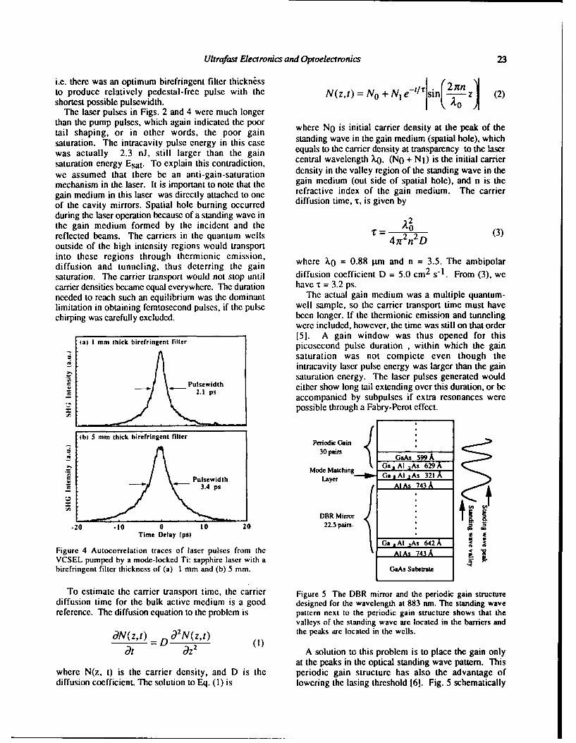
Ultrafast Electronics and Optoelectronics 23
i.e. there was an optimum birefringent filter thicknessto produce relatively pedestal-free pulse with the N(z,t) = No + N1 e-t/r sin z (2)shortest possible pulsewidth.
The laser pulses in Figs. 2 and 4 were much longerthan the pump pulses, which again indicated the poor where No is initial carrier density at the peak of thetail shaping, or in other words, the poor gain where NO i n the gai ediumity pat h ole), whesaturation. The intracavity pulse energy in this case standing wave in the gain medium (spatial hole), whichwas actually 2.3 nJ, still larger than the gain equals to the carrier density at transparency to the lasersaturation energy Esat. To explain this contradiction, central wavelength X0, (NO + NI) is the initial carrierwe assumed that there be an anti-gain-saturation density in the valley region of the standing wave in themechanism in the laser. It is important to note that th gain medium (out side of spatial hole), and n is themechnis inthelasr. t i imortnt o nte hatthe refractive index of the gain medium. The carriergain medium in this laser was directly attached to one refractive id gin mTof the cavity mirrors. Spatial hole burning occurred diffusion time, 't, is given byduring the laser operation because of a standing wave inthe gain medium formed by the incident and the 0L(0reflected beams. The carriers in the quantum wells 247 (3)outside of the high intensity regions would transportinto these regions through thermionic emission,diffusion and tunneling, thus deterring the gain where 0o = 0.88 c ic m and n = 3.5. The ambipolarsaturation. The carrier transport would not stop until diffusion coefficient D = 5.0 cm 2 s From (3), wecarrier densities became equal everywhere. The duration have t = 3.2 ps.needed to reach such an equilibrium was the dominant The actual gain medium was a multiple quantum-limitation in obtaining femtosecond pulses, if the pulse well sample, so the carrier transport time must havechirping was carefully excluded, been longer. If the thermionic emission and tunneling
were included, however, the time was still on that order
I mm thick birerringent filter [5]. A gain window was thus opened for thisa) 1 ipicosecond pulse duration , within which the gain
saturation was not compiete even though theintracavity laser pulse energy was larger than the gainsaturation energy. The laser pulses generated would
2 1 Pse either show long tail extending over this duration, or beA •ps accompanied by subpulses if extra resonances were
-. possible through a Fabry-Perot effect.
(b) 5 mm thick birefringent filter P i
30 pairsG ,g G-aAs 59 AMode Matching __ GasAl.2As 321A
PulseicithLayer3.4 p A[iAs 743 A
DBR Mirror
-20 -10 0 10 20 225 pairs "Time Delay (ps) _
Ga AI As 642AFigure 4 Autocorrelation traces of laser pulses from the Al As 743AVCSEL pumped by a mode-lockcd Ti: sapphire laser with abirefringent filter thickness of (a) 1 mm and (b) 5 mm. GaAs Sutrate
To estimate the carrier transport time, the carrier Figure 5 The DBR mirror and the periodic gain structurediffusion time for the bulk active medium is a good designed for the wavelength at 883 run. The standing wavereference. The diffusion equation to the problem is pattern next to the periodic gain structure shows that the
valleys of the standing wave are located in the barriers and
dN(z't) d 2 2N(z't) the peaks are located in the wells.
d D dZ2 A solution to this problem is to place the gain onlyat the peaks in the optical standing wave pattern. This
where N(z, t) is the carrier density, and D is the periodic gain structure has also the advantage ofdiffusion coefficient. The solution to Eq. (1) is lowering the lasing threshold [6]. Fig. 5 schematically
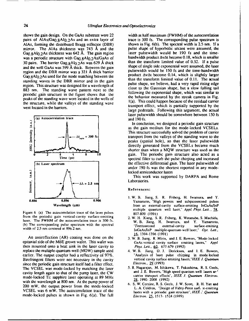
24 Ultrafast Electronics and Optoelectronics
shows the gain design. On the GaAs substrate were 22 width at half maximum (FWHM) of the autocorrelationpairs of AlAs/Ga0.8AI0.2As and an extra layer of trace is 300 fs. The corresponding pulse spectrum isAlAs, forming the distributed Bragg reflector (DBR) shown in Fig. 6(b). The spectral width is 2.5 nm. If amirror. The AlAs thickness was 743 A and the pulse shape of hyperbolic secant were assumed, theGao.8Al0.2As thickness was 642 A. The gain region laser pulsewidth would be 190 fs and the time-was a periodic structure with Ga0.8Al0.2As/GaAs of bandwidth product AvAt become 0.18, which is smaller30 pairs. The barrier Ga0.8AI0.2As was 629 A thick than the transform limited value of 0.32. If a pulseand the well GaAs was 599 A thick. Between the gain shape of single side exponential were assumed, the laserregion and the DBR mirror was a 321 A thick barrier pulsewidth would be 150 fs and the time-bandwidthGao.8AI0.2As used for the mode matching between the product AvAt become 0.14, which is slightly largerstanding waves in the DBR mirror and in the gain than the transform limited value of 0.11. The actual
region. This structure was designed for a wavelength of pulse shape, we believe, had a very rapid rising edge
883 nm. The standing wave pattern next to the close to the Gaussian shape, but a slow failing tail
periodic gain structure in the figure shows that the following the exponential shape, which was similar to
peaks of the standing wave were located in the wells of the behavior measured by the streak camera in Fig.the structure, while the valleys of the standing wave 1(a). This could happen because of the residual carrier
were located in the barriers, transport effect, which is partially supported by thelarge pedestals. Following this argument, the actuallaser pulsewidth should be somewhere between 150 fs
(a) Autocorrelation trace and 190 fs.In conclusion, we designed a periodic gain structure
as the gain medium for the mode-locked VCSELs.•o rsThis structure successfully solved the problem of carrier3t = transport from the valleys of the standing wave to the
peaks (spatial hole), so that the laser pulsewidthdirectly generated from the VCSELs became muchshorter than when a MQW structure was used as the
0 2 4 5 8 10 gain. The periodic gain structure also acted as aTime (ps) spectral filter to curb the pulse chirping and increased
(b) Laser spectrum the effective differential gain. The laser pulsewidth ofunder 190 fs was the shortest reported in any mode-locked semiconductor lasers
This work was supported by DARPA and RomeLaboratories.
• .- AX = 2.5 nm
References:
- 1 1.W. B. Jiang, S. R. Friberg, H. Iwamura. and Y.0.886 0.896 0.906 Yamamoto, "High powers and subpicosecond pulses
Wavelength (pim) from an external-cavity surface-emitting lnGaAs/InP
multiple quantum well laser," Appl. Phys. Lett., 58,Figure 6 (a) The autocorrelation trace of the laser pulses 807-809 (1991)from the periodic gain vertical-cavity surface-emitting 2. W. H. Xiang. S. R. Friberg, K. Watanabe, S. Machida.laser. The FWHM of the autocorrelation trace is 300 fs. W. B. Jiang, H. Iwamura, and Y. Yamamoto,(b) The corresponding pulse spectrum with the spectral "Femtosecond external-cavity surface-emittingwidth of 2.5 nm centered at 896.2 rum. lnGaAs/lnP multiple-quantum-well laser," Opt. Len.,
16, 1394-1396 (1991)An antireflection (AR) coating was done on the 3. W. B. Jiang, R. Mirin, and I. E. Bowers. "Mode-locked
epitaxial side of the MBE grown wafer. This wafer was GaAs vertical cavity surface emitting lasers," Appl.then mounted onto a heat sink in the laser cavity to Phys. Lett.. 60. 677-679 (1992)replace the multiple-quantum-well (MOW) sample used 4. W. B. Jiang, D. J. Derickson, and J. E. Bowers,earlier. The output coupler had a reflectivity of 97%. "Analysis of laser pulse chirping in mode-lockedBirefringent filters were not necessary in the cavity vertical cavity surface emitting lasers,"IEEE J. Quantumsince the periodic gain structure itself had a filter effect. Electron., 29 (1993)The VCSEL was mode-locked by matching the laser 5. R. Nagarajan, M. Ishikawa, T. Fukushima, R. S. Geels.cavity length again to that of the pump laser, the CW and J. E. Bowers, "High speed quantum-well lasers az-'
mode-locked Ti: sapphire laser operating at 89 MHz carrier transport effects", IEEE J. Quantum Electron.
with the wavelength at 800 nm. At the pump power of a. 1990- 2008 (1992)
200 mW, the output power from the mode-locked 6. S, W. Corzine, R. S. Geels, J. W. Scott, R. H. Yan andL. A. Coldren, "Design of Fabry-Perot surf. :e-emitting
VCSEL was 6 mW. The autocorrelation trace of the lasers with a periodic gain structure". IEEE.'. Quantummode-locked pulses is shown in Fig. 6(a). The full Electron. 2.5 1513- 1524 (1989)
Picosecond Gain Dynamics in Vertical Cavity SurfaceEmitting Laser: Transient Carrier Heating and
Gain Enhancement
Gary Wang, Radhakrishnan Nagarajan, Dan Tauber, and John E. Bowers
Department of Electrical and Computer Engineering, University of California,Santa Barbara, California 93106
Abstract Theory
Enhancement of resonance frequency up to 87 GHz has Previous studies on gain switching of in-plane lasersbeen observed in a vertical cavity surface emitting laser. have shown the modulation bandwidth and resonanceWe derive an analytical expression for the intrinsic gain frequency of the laser are related [3]. The gain switchedsuppression factor based on carrier heating. The theory laser dynamics can be modeled using the coupledshows good agreement with the published experimental carrier-photon rate equations [3),value of c = 1.5x10⁻¹⁷cm 3 for in-plane lasers. For thefirst time, we predict and experimentally observe a &VN - _] Nnegative gain suppression factor for particular laser =- -v(N,T,,GT()S (,)designs. A negative gain suppression factor can lead to (1t qVthe elimination of damping in semiconductor lasers. dS SUsing vertical cavity surface emitting lasers, we - =Fv G(N,T,&,•,,T,)S- -Sobserve a negative gain suppression factor of dt vi.2.2x10- 17 cm 3 .
where N is the carrier density, S is the photon density,mi is the internal quantum efficiency, r is theconfinement factor, v. is the group velocity, zn and cp
Introduction are the carrier and photon lifetimes, respectively. Theimportant result from the analysis of Eqs. (1) is that the
High speed modulation of vertical cavity surface resonance frequency of the laser is given by the inverseemitting lasers (VCSELs) is essential for wide of the geometrical mean between the stimulatedbandwidth, on-chip optical interconnects[ I). From a emission lifetime and the intracavity photon lifetime[3].previous optical gain switching experiment, an Due to the ultra short cavity length, a shorter photonintrinsically wide bandwidth for VCSELs has been lifetime can be acheived more easily for VCSELs thanpredicted[2]. In recent demonstrations of an electrically for in-plane lasers, even though the mirror reflectivitiespumped VCSEL, the bandwidth has been limited by RC of VCSELs are significantly higher[2]; therefore, weparasitics due to the high series resistance of current can expect an enhancement of the resonance frequencyinjecting mirrors. However, to determine the intrinsic and the intrinsic modulation bandwidth for VCSELs.lndynamic response beyond the RC limit, electrical gain addition, the temporal variation of gain described byswitching experiments can be used. In this paper, we Eq. (1) depends significantly on the dynamics of thepresent the theory and experimental results of longitudinal mode. For structures such as distributedpicosecond dynamics of electrically gain switched feedback (DFB) lasers or VCSELs, the lasing mode isVCSELs. Most importantly, we predict and observe a restrained by the cavity design, whereas for in-planenegative gain suppression factor for lasers with a laser, the lasing mode always occurs at the gain peak.positive temperature derivative of gain. Furthermore, Furthermore, the gain dynamics at the lasing mode canwe propose that the damping limit can be greatly be significantly different if the transient variation ofreduced with proper design. temperatures are considered.
OSA hocuamnpa b•r4 EWecs andOpeoefloerca 1993. VoL.14 25Jqptq tu oand Uuw Mish (*&)* 1993 Optdcd Sodu*y dAmpla
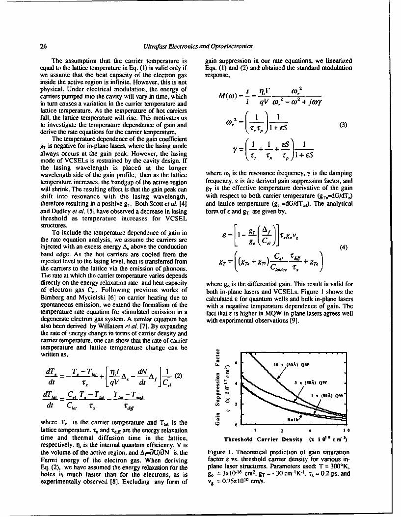
26 Ultrafast Electronics and Optoelectronics
The assumption that the carrier temperature is gain suppression in our rate equations, we linearizedequal to the lattice temperature in Eq. (1) is valid only if Eqs. (1) and (2) and obtained the standard modulationwe assume that the heat capacity of the electron gas response,inside the active region is infinite. However, this is notphysical. Under electrical modulation, the energy of S 70) r2
carriers pumped into the cavity will vary in time, which M(0)) = - =- 2in turn causes a variation in the carrier temperature and i qV ,2 - (0 + jM)Ylattice temperature. As the temperature of hot carriersfall, the lattice temperature will rise. This motivates us 2 1 1to investigate the temperature dependence of gain and Wr0) = (3)derive the rate equations for the carrier temperature.
The temperature dependence of the gain coefficient (gT is negative for in-plane lasers, where the lasing mode Y= 1 1 ES 1always occurs at the gain peak. However, the lasing r. 1 + eSmode of VCSELs is restrained by the cavity design. Ifthe lasing wavelength is placed at the longerwavelength side of the gain profile, then as the lattice where tor is the resonance frequency, y is the dampingtemperature increases, the bandgap of the active region frequency, E is the derived gain suppression factor, andwill shrink. The resulting effect is that the gain peak can gT is the effective temperature derivative of the gainshift into resonance with the lasing wavelength, with respect to both carrier temperature (gT.=dG/dTj)therefore resulting in a positive gT. Both Scott et al. [4] and lattice temperature (gn=dG/dT,.). The analyticaland Dudley et al. [51 have observed a decrease in lasing form of E and gT are given by,threshold as temperature increases for VCSELstructures.
To include the temperature dependence of gain in E= 1- a"gthe rate equation analysis, we assume the carriers are g. C,injected with an excess energy Ak above the conduction (4)band edge. As the hot carriers are cooled from the )C_ -SLinjected level to the lasing level, heat is transferred from gT = (gr, + gn) + gr.the carriers to the lattice via the emission of phonons. C--, •The rate at which the carrier temperature varies dependsdirectly on the energy relaxation rate and heat capacity where g. is the differential gain. This result is valid forof electron gas C61 . Following previous works of both in-plane lasers and VCSELs. Figure 1 shows theBimberg and Mycielski [6] on carrier heating due to calculated E for quantum wells and bulk in-plane lasersspontaneous emission, we extend the formalism of the with a negative temperature dependence of gain. Thetemperature rate equation for stimulated emission in a fact that c is higher in MQW in-plane lasers agrees welldegenerate electron gas system. A similar equation has with experimental observations [9].also been derived by Willatzen et al. [7]. By expandingthe rate of .nergy change in terms of carrier density andcarrier temperature, one can show that the rate of carriertemperature and lattice temperature change can bewritten as,
6 lox (BOA) QW
di T - T_+u2-IA, dN A ]1 (2 ) ... Qdt LqV dt .JC , 4 3 X, Qw
dT',, C., T. TT, T1 -T ,-,k I X (BOA) QWw
U o -dt C, 1. Ad~ 2l
where T, is the carrier temperature and T1t is the rlattice temperature.;,, and ¢dff are the energy relaxation 1 2 4 1 0
time and thermal diffusion time in the lattice, Threshold Carrier Density (x 1 0" cm")respectively. Thi is the internal quantum efficiency, V isthe volume of the active region, and Af-=U/)N is the Figure 1. Theoretical prediction of gain saturationFermi energy of the electron gas. When deriving factor E vs. threshold carrier density for various in-Eq. (2), we have assumed the energy relaxation for the plane laser structures. Parameters used: T = 300°K,holes is much faster than for the electrons, as is g = 3x10- 6 cm 2, g' = -30 cm-'K', T = 0.2 ps, andexperimentally observed [81. Excluding any form of vg = 0.75x 1010 cm/s.
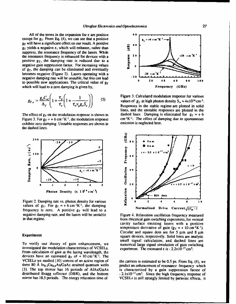
Ultrafast Flectronics and Optoelectronics 27
All of the terms in the expansion for E are positive 60 - - - ..........except for gT. From Eq. (4), we can see that a positive T= +6 C 16 'C-
gT will have a significant effect on our result. A positive .-- 40
g-r yields a negative c, which will enhance, rather than
suppress, the resonance frequency of the lasers. Whilethe resonance frequency is enhanced for devices with a --2 2
positive gT, the damping rate is reduced due to anegative gain suppression factor. For increasing values 0 •of gT, the damping can be eliminated and eventuallybecomes negative (Figure 2). Lasers operating with a -20 c,. 'K'negative damping rate will be unstable, but this can lead -0 2 4 6. s 100to possible new applications. The critical value of gTwhich will lead to a zero damping is given by, Frequency (GHz)
C +(, , Figure 3. Calculated modulation response for various---- =1--, (I v-P(I+ (5) values of gT at high photon density So = 4x10 16 cm-3.
A .,Responses in the stable regime are plotted in solidlines, and the unstable responses are plotted in the
The effect of gT on the modulation response is shown in dashed lines. Damping is eliminated for gT = + 6Figure 3. For gT- = + 6 cm- KV, the modulation response cm-'K-1. The effect of damping due to spontaneousexhibits zero damping. Unstable responses are shown in emission is neglected here.the dashed lines.
200 11 a 0 02 Samn
0I I
100 60 _ e2.2 110 CM
a.
value ofggFrg =+6c-K them'K dampi0
5+
PhotonsurDensityting(la10s'wthcampsitiv
a-
valuesatofegderFortive o +a6ncmgK =,+the damping
Circular and square dots are for 5 lam and 8 j•tmExperiment square devices, respectively. Solid lines are analytic
small signal calculation, and dashed lines areTo verify our theory of gain enhancement, we numerical large signal simulation of gain switchinginvestigated the modulation characteristics of VCSELs. experiment. The estimated + is - 2.2x 10'17 cm3.From calculation of gain at the lasing wavelength, thedevices have an estimated g= of + 10 cm pK-m TheVCSELs we studied [10] consist of an active region of the carriers is estimated to be 0.5 ps. From Eq. (4), wethree 80 A mno 2Gao 8As/GaAs strained quantum wells predict an enhancement of resonance frequency which
131. The top mirror has 16 periods of AlAs/GaAs is characterized by a gain suppression factor ofdistributed Bragg reflctor (DBR), and the bottom - 2.1x 10Ccm3. Since the high frequency response ofmirror has 18.5 periods. The energy relaxation time of VCSELs is still strongly limited by parasitic effects, itFro cac lto of gi n .... th lasin...vle......h
28 Utrafasr Electronics and Oproelecironics
would be difficult to accurately determine the relaxation is supported by the NSF Science and Technologyoscillation frequency and damping frequency from Center of Quantized Electronic Structures, Grantmodulation measurements. Instead, we measure the #DMR 91-20007.resonance frequency from CW relative intensity noise(RIN) measurements (Figure 4). However, as the laseris driven far above threshold, CW heating in the active Referenceslayer severely limits the usefulness of this technique. Toavoid this problems, we also measured the pulsed 1. M. W. Maeda, C. Chang-Hasnain, A.dynamic characteristics of the device with a streak Vonlehmen, H. Izadpanah, C. Lin, M. Z.. lqbal,camera. A step recovery diode is used to generate 12V L Florez, J. Harbison, "Multigigabits/s operation100 ps pulses at an 80 MHz repetition rate. A of 16-wavlength veritcal-cavity surface emittingHamamatsu M1955 streak camera in the synchro-scan laser array," Photonic Tech. Let. 3 863 (1991)mode is used to monitor the gain switched output. Theperiod of the large signal relaxation oscillations is 2. J. R. Karin, L. G. Melcer, R. Nagarajan, J.E.measured and the inverse of this period is plotted in Bowers, S.W. Corzine, P.A. Morton, R. S.Figure 4, along with the CW RIN data. This figure Geels, L. A. Coldren, "Generation of picosecondshows data for two VCSELs of different sizes. pulses with a gain-switched gaas surfaceMaximum relaxation oscillation frequencies of 87 and emitting laser," Appl. Phys. Let. 57 963 (1990)71 GHz are observed from 5 gim and 8 gtm devices,respectively. 3. J. E. Bowers, "High speed semiconductor laser
The figure also shows calculations based on positive design and performance," Solid State Electron.,and negative e. It can be seen that the data matches 30, 1-11 (1987)quite well with an E of - 2.2x10 17 cm 3, in agreementwith the estimated value. Note that these experimental 4. J. W. Scott, B. Young, S. W. Corzine, L. A.results cannot be understood using conventional Coldren, "Modeling temperature effects andexpressions for differential gain and damping spatial hole burning to optimize vertical cavityfrequency. The final calculation shown in Figure 4 is a surface emitting laser performance," To belarge signal calculation of the inverse of the relaxation published in IEEE J. Quantum Electron.oscillation time based on a numerical integration of therate equations including carrier heating. The inverse of 5. J. J. Dudley, M. Ishikawa, D. I. Babic, B. I.the relaxation oscillation ringing time is approximately Miller, R. Mirin, W. B. Jiang, J. E. Bowers, E.the same as the on-state small signal resonance L. Hu., " 144 0C operation of 1.3 um InGaAsPfrequency, as we assumed in the previous paragraph. vertical cavity lasers on GaAs substrates," To beWe have verified this relation also for the case of very published in Appl. Phys. Lett.high driving signals (50 times threshold) and very highrelaxation oscillation frequencies (90 GHz). It can be 6. D. Bimberg, J. Mycielski, "The recombination-seen theoretically that the small signal and the large induced temperature change of non-equilibriumsignal results are quite similar. charged carriers," J. Phys. C: Solid State Phys.
19 pp. 2363-2373, (1986)Conclusions
7. M. Willatzen, A. Uskov, J. Mork, H. Olesen, B.In conclusion, we have analyzed the high frequency Tromborg, A. P. Jauho, "Nonlinear gaindynamics of semiconductor lasers including carrier suppression in semiconductor lasers due toheating. The calculated value of E agrees with published carrier heating," IEEE Photonics Technologyresults for in-plane lasers. The theory is able to explain Lett., vol. 3 606-609 (1991)the variation of e between bulk and MQW lasers.Furthermore, we have predicted that with proper cavity 8. J. Shah, "Hot carriers in quasi-2D polardesign, one could observe an enhancement in the semiconductors," IEEE J. Quantum Electron.,resonance frequency and elimination of damping in QE-22, 1728-1743 (1986).VCSELs or DFB lasers. An enhancement in theresonance frequency was observed in high speed 9. K. Uomi, T. Tsuchiya, M. Aoki, N. Chinone,VCSELs. "Oscillation wavelength and laser structure
dependence of nonlinear damping effect inAcknowledgments semiconductor lasers," Appl. Phys. Lett. 58
675-677 (1991)The authors would like to thank D. Bimberg, E. Ippen,K. Hall, B. Gomatam, D. Babic, J. Karin, and R. Helkey 10. R. S. Geels, S. W. Corzine, L. A. Coldren,for many informative discussions, and R. S. Geels, J. "InGaAs vertical-cavity surface emitting lasers,"Scott, B. Young and L. A. Coldren for providing the IEEE J. Quantum Electron., QE-27, 1359-1367VCSELs for the gain switching experiments. This work (1991)
Transient Pulse-Response of InGaAs/InGaAsPDistributed Feedback Lasers for Multigigabit
Transmission Systems
L. Kovac, C. Kaden, and H. Schweizer4. Physikalisches Instiut, Universitdt Stultgarz, Pfaffenwaldring 57,
7000 Stuttgart-80, Germany
NL Klenk, R. Weinmann, E. ZielinskiAlcatel-SEL, Research Center, Lorenzstr. 10, 7000 Stuttgart-40, Germany
Abstract The light is coupled out by a slab waveguide.The optical modulation of the DFB was carried
Optical excitation with picosecond pulses is out by a pulse-compressed cw mode-locked Nd-YAGused to investigate high frequency modulation laser with a full width at half maximum (FWHM)properties of distributed feedback (DFB) lasers. of 9 ps. The up-converted signal was detected byTypical time constants like the rise and fall an optical multichannel analyzer.time and te full width at half maximum of the For a theoretical description of laser dynam-laser response were investigated. We show that ics coupled rate equations were used. Intrinsicintrinsic carrier dynamics mainly determine the carrier dynamics are included by considering a 3transient behavior of the lasing pulse. A theo- level system.retical analysis of a 3 level system consideringcarrier dynamics yields coupled rate equations,which are appropriate for a description of the Experimental resultsexperiments. Furthermore spectral characteris-tics of DFB lasers in the picosecond time scale The response of the device on a pulsed opticalis analyzed with respect to multi- and single excitation is demonstrated in Fig. 1. The tran-mode operation. sient spectra indicate the main characteristics
of the lasing process: the intensity of the la-ser mode increases and vanishes within 80 ps.Introduction
InGaAs/InGaAsP semiconductor lasers are key de-vices for optical-communication systems. Single = 232. n to,mode devices like DFB lasers are necessary to 230 psmeet the requirements for high data-rate systemsbased on optical fiber transmission links. _ _ 208p"
A powerful method to investigate fast proces- p -ses in semiconductor lasers is the technique oflight frequency up-conversion [1]. A careful . Figure 1.adjustment of the excitation pulses in time and 19 . Transientfrequency domain results in a temporal and spec- - s atral resolution simultaneously, which allows to -82 e DFB mode atquantify the temporal behavior like the rise "Ktime and the fall time of the laser emission and Ti periodwhich enables a direct observation of the car- -- 18 " of 232.5 nm
Crier dynamics by transient spectra. .SIn this contribution we will discuss the
pulse response of multiple quantum well MQW(Lz = 8 nm) InGaAs/InGaAsP DFB lasers optimized " 152 p.for carrier- and light-confinement. The reso- 8.nators are 500 gm long and consist of DFB gra- 853.5 855.0tings of different periods (A= 220 nm - 250 nm). energy [meV]
OSA Prowdagon Uklar1 Ekemroacs an Opwkaroxcks 1993 VoL 14 29JaqAep Mhh md Unahg Mishr (*&)0 993 Optkd Socklu ofAaerica
30 Ultrafast Electronics and Optoelectronics
During this time, the lasing mode is chirping. starts there is a blue-shift. When threshold isA detailed analysis of the lasing process can reached an abrupt chirping of about 0.6 meV down
be carried out on the base of Fig. 2. The inte- to lower energies is observed. This can be un-grated intensity of the DFB mode (left axis) is derstood by the dependence of the effective re-depicted versus time. At first the spontaneous fractive index on the carrier density. First theemission, respectively the amplified spontaneous carrier population in the quantum wells increa-emission of the device is detected. After a ses. When threshold is reached the subsequentdelay-on time of about 150 ps lasing starts. The reduction of the carrier density reduces therise time of the single mode is 7 ps, the fall refractive index causing a red-shift. The changetime is 18 ps. At later times the emission pas- 8n of the refractive index due to free carrierses into the spontaneous, respectively the am- density N can be described by 141,plified spontaneous emission.
One single pulse with a FWHM of 29 ps is ob-served, no relaxation oscillations appear. This n = - N q2 / (2 m/p Eon)can be explained by a build-up of the carrierdensity and a subsequent recombination via stim- where q is the electron charge, mn the effec-ulated emission. tive mass of the electron and hole respectively,
co the lasing angular frequency, EQ the permit-o.. 2 tivity of free space and n the refractive index
T--iA 232. m: in the absence of free carriers.0.8540 This equation yields an estimation for the
carrier density in the active region, which is"e oreduced by the stimulated emission. The shift of
7 0.6 meV corresponds to a drop of the carrierP density during the lasing process, which is in
C the range of the threshold density (-10] cm 3).0.&W4 The discussion above clearly demonstrates
that the temporal behavior of the laser emission10' o.832 characterized by the delay-on time, the rise ando00 100 20 inn 4 2 fall time, the FWHM and the chirp of the mode
time [ps] corresponds to intrinsic carrier dynamics. Re-laxation and diffusion of carriers are tempera-
Figure 2. ture dependent, so measurements at 2 K and 77 KSolid line: intensity of the DFB mode versus were performed to show the influence of intrin-time sic processes on the time behavior of the lasingCrosses: energy shift of the DFB mode versus mode. The results are demonstrated in Fig. 3,time where the intensity of the lasing mode is depic-
ted versus time.In the case of optical excitation electron- At 2 K the distinction between spontaneous,
hole pairs are mainly generated in the energy respectively amplified spontaneous emission andlevels of the InGaAsP-barriers. The intrinsic the lasing emission is less well defined com-processes of relaxation, diffusion and capture pared to the threshold points at 77 K. The riseof carriers from the barriers into the quantum time of about 18 ps and the lasing period with awells populate the energy level responsible for FWHM of 83 ps appear longer than at 77 K. At 2 Klasing [2][3]. Recombination of electron-hole a prolonged diffusion and relaxation time leadpairs leads to spontaneous, respectively ampli- to a delayed and prolonged capture of carriersfled spontaneous emission. When threshold densi- into the lasing level in comparison to 77 K [5].ty is exceeded, lasing starts. The intensity of These results are confirmed by a comparisonthe DFB mode shows a steep rise. The interplay of different laser resonators with grating pe-between the population of the lasing level and riods between 227.5 nm and 235 nm. The Braggthe reduction of the carrier density via stimu- wavelengths of these resonators cover the gainlated emission determines the duration of the region of the semiconductor material. The laserlasing process. When the carrier density is re- emission at 2 K starts and ends less abrupt andduced below threshold density, lasing ends and lasts longer compared to 77 K. The FWI-Ms at 2 Kspontaneous, respectively amplified spontaneous are between 40 ps and 80 ps and at 77 K betweenemission reduce the carrier density further. 17 ps and 50 ps. Hereby the FWHMs increase with
The intrinsic carrier transport and relaxa- increasing grating period. For a given gratingtion effects in conjunction with spontaneous and period the FWHM at 2 K is about a factor of 1.5stimulated emission lead to the mostly undesira- to 2.5 longer than at 77 K. From these data weble chirping of the lasing mode. In Fig. 2 the conclude, that different time constants of theenergy position of the DFB mode (right axis) intrinsic relaxation and transport effects atduring and slightly before and after lasing is 2K and at 77K determine mainly the timeplotted versus time. Before laser emission behavior of the lasing pulse.
Ultrafast Electronics and Optoelectronics 31
population rate from the excited energy level,A- 232.5 nm ii) the rate given by the spontaneous recombina-
r17 tion lifetime •sp and iii) the stimulated emis-T - 77,, I- 2 X sion rate with the optical gain coefficient (x,
the transparency density Ntr and the photon den-sity S. The spontaneous recombination lifetime"-s depends on the carrier density, which is ta-kepn into account by a sum of the non-radiative,the radiative and the Auger recombination. Non-linearities of the optical gain coefficient are
•G considered by the gain compression factor c.A The rates for the photon density are given by
i) the stimulated term with the confinement fac-1010 100 200 :300 400 tor F, ii) the photon lifetime c, which de-
time [psi scribes the photon losses and ii the fractionP3 of the spontaneous contribution emitted into
Figure 3. the lasing mode.Intensity of the DFB mode at different Fig. 4 shows the temporal behavior of thetemperatures photon density for different values of the re-
laxation constant treI. The excitation conditionTheoretical description corresponds to the experimental preparation of
the system and leads to one single responseFor the theoretical description of the experi- pulse in the time domain. With a relaxationments a 3 level system is --- -1. We assume opti- constant of 10 ps a FWHM of 34 ps is obtained.cal Lorentzian-shaped pulses g(t) (FWHM = 9ps) This FWHM value approaches the measured one atcal oretzin-sape pusesg~t (FLIM77 K. When the relaxation constant becomesgenerating a number of electron-hole pairs n7 .We h eaaincntn eoein an excited energy level. From this level p i C longer the rise time and the FWHMs increase. Forin a exitedenegy lvel Fro ths leel ir- a relaxation constant of 300 ps a FWHM of 80 psfusion, relaxation and capture of carriers into a obtin ch orresps t o 80 m sthe lasing level of the QW are described by an is obtained, which corresponds to the measuredoverall relaxation constant TrI: data at 2 K. For all excitation intensities,
longer relaxation constants lead to longer risetimes and FWHMs of the response pulses.
= g(t) - exc From comparison of the theoretical resultsat Trel with the experimentally found temperature de-
pendent laser dynamics we conclude that DFB la-The generation of electron-hole pairs was ser dynamics is mostly determined by carrier
carried out by an excitation stripe along the dynamics.resonator with a cylindrical lens. So a homoge- A new effect has been observed, which may
neous carrier density along the resonator can be influence bit error rates seriously at extremelybuilt up. This is the first condition, which high modulation speed. As mentioned above, theallow us the use of spatially averaged rate DFB grating is joined to an output-coupler,equations [6] for the theoretical description of which leads to Fabry-Perot (FP) modes, if gainthe time behavior of one lasing mode. The second is high enough. At a temperature of 2 K we ob-condition requires, that time constants for theoccupation of the lasing level are longer thanthe round-trip time of the light-wave in theresonator (- 10 ps). Considering only the FWHM3f the excitation pulse (9 ps), the limit of E to"4validity is reached. When the intrinsic proces-ses at low temperature are taken into account, 100 Pethan the effective occupation time of the lasing 3
level becomes longer and the following rates can
be used: 1o"
aN nexc N IS= . . (.(N-Ntr).S 9L
at V.- re t lsp o1w
OS S N 0 200 40 0oo 1000a = F.Ca.(N-Ntr).S - - + r.p.-.. time [psItt"p tsp
Figure 4.The rates which determine the change of the Calculated temporal behavior of the photon den-
carrier density N in the lasing level are i) the sity for different relaxation constants
32 Ultrafast Electronics and Optoelectronics
served a coupling of the DFB mode and the FP Acknowledgmentsmodes which appear at the gain maximum. Firstthe FP modes rise. Still during the increase of The authors thank M.H.Pilkuhn, G.Bacher, G.Mayerthe amplified sponztaaý,;,. emission around the and E.Lach for stimulating and valuable discus-DFB mode the intensity of the FP modes decrea- sions and expert experimental assistance.ses. When the DFB mode reaches threshold the FPmodes are quenched.
From these data we conclude, that the thresh-old gain of the FP is reached very early about160 ps before a stable DFB mode builds up. Abuilt up time of roughly 16 round-trips is ne- Referencescessary to stabilize the DFB mode. The instan-taneous appearance of the FP-modes after the [1] J.Shah, "Ultrafast Luminescence Spectro-excitation pulse suggests a fast relaxation pro- scopy Using Sum Frequency Generation",cess. In the sub-picosecond time domain a non- IEEE Journal of Quantum Electronics,equilibrium distribution of electron and holes Vol.24, No.2, pp. 276-288, (1988)is changed into a Quasi-Fermi distribution effi-ciently via carrier-carrier scattering [7]. [2] A.Weller, P.Thomas, J.Feldmann, G.Peter,Therefore the carriers become redistributed over E.O.Gdbel, "Model Calculations of Dif-a wide energy range. At 2 K the gain conditions fusion Limited Trapping Dynamics inallow multimode emission for a short time of 1 Quantum Well Laser structures", Appliedto 3 round-trips. A following relaxation via Physics A 48, pp. 509-515 (1989)optical and acoustic phonons leads to a built upof the DFB mode, which is preferred by the gra- [3] W.Rideout, W.F.Sharfin, E.S.Koteles,ting M.O.Vassell, B.Elman, "Well-Barrier Hole
Burning in Quantum Well Lasers", IEEEPhotonic Technology Letters, Vol.3,
Conclusion No.9, pp. 784-786, (1991)
In summary we have studied the transient be- [4] F.R.Nash, "Mode guidance parallel to thehavior of a InGaAs/InGaAsP MQW DFB laser after junction plane of double-heterostructurean optical excitation with picosecond-pulses. GaAs lasers", J.Appl.Phys., Vol.44,
The pulse response on a 9 ps excitation pulse No.10, pp. 4696-4707, (1973)is a single pulse, which is determined by relax-ation and diffusion processes of carriers into [5] B.Deveaud, F.Clerot, A.Regreny, K.Fuji-the QWs: the FWHMs at 77 K are between 17 ps and wara, K.Mitsunaga, J.Ohta, "Capture of50 ps and at 2 K between 40 ps and 80 ps. photoexcited carriers by a laser struc-
The analysis of a 3 level system results in ture", Appl.Phys.Lett.55 (25), pp. 2646-coupled rate equations for the carrier and pho- 2648, (1989)ton density. The solutions describe the temporalbehavior of the experiment: Longer relaxation [61 K.Y.Lau, A.Yariv, "High-Frequency Cur-constants for the intrinsic transport avd rela- rent Modulation of Semiconductor Injec-xation processes y, J longer FWHIMs for the tion Lasers" in Semiconductor and Semi-pulse-response in agreement with the temperature metal, Vol.22, Pai B-dependent experimental findings.
At 2 K multimode (FP) and DFB emission show [7] T.Elsaesser, Jagdeep Shah, Lucio Rota,mode competition effects. Instantaneously after Paolo Lugli, "Initial Thermalization ofthe pump pulse a low threshold for FP modes Photoexcited Carriers in GaAs Studied byleads to short time duration (1-3 round-trips). Femtosecond Luminescence Spectroscopy",DFB laser emission stabilizes after several Phys.Rev.Letters, Vol.66, No.13, pp.round-trips. 1757-1760 (1991)
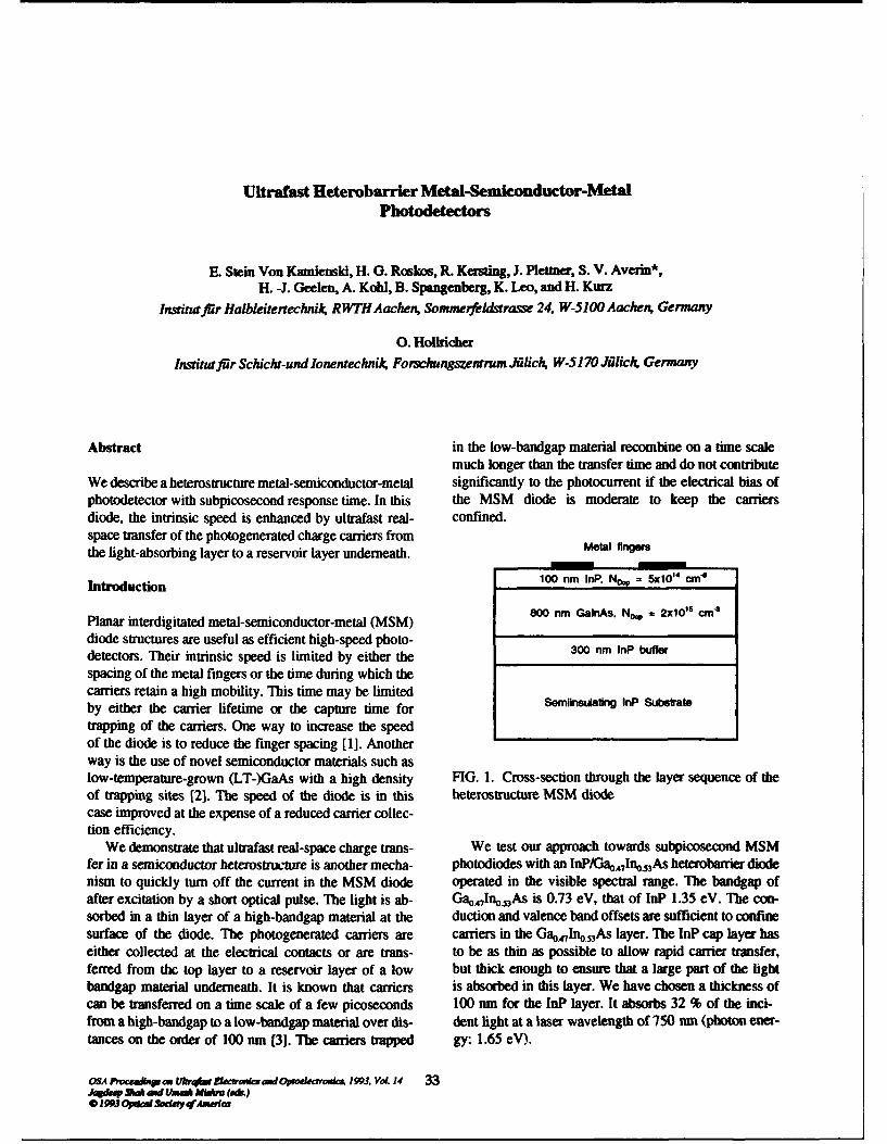
Ultrafast Heterobarrier Metal-Semiconductor-MetalPhotodetectors
E. Stein Von Kamienski, H. G. Roskos, R. Kersting, J. Plettner, S. V. Averin*,H. -J. Geelen, A. Kohl, B. Spangenberg, K. Leo, and H. Kurz
InsttutJfir Halbleiterrechnik, RWTHfAachen, Sommerfeldstrasse 24, W-5100 Aachen, Germany
0. Holkicher
Institutfir Schicht-und Ionentechnik, Forschungszentrum JAlich, W-5170 JMlich, Germany
Abstract in the low-bandgap material recombine on a time scalemuch longer than the transfer time and do not contribute
We describe a heterostructure metal-semiconductor-metal significantly to the photocurrent if the electrical bias ofphotodetector with subpicosecond response time. In this the MSM diode is moderate to keep the carriersdiode, the intrinsic speed is enhanced by ultrafast real- confined.space transfer of the photogenerated charge carriers fromthe light-absorbing layer to a reservoir layer underneath. Metal fngers
Introduction 100 nm InP. N., = 5x10 1 ' cm4
Planar interdigitated metal-semiconductor-metal (MSM) 800 nm GalnAs, N,, . 2xl0'8 cm4
diode structures are useful as efficient high-speed photo-detectors. Their intrinsic speed is limited by either the 300 nm InP buffer
spacing of the metal fingers or the time during which thecarriers retain a high mobility. This time may be limitedby either the carrier lifetime or the capture time for Semiinsmabing InP Substat.
trapping of the carriers. One way to increase the speedof the diode is to reduce the finger spacing [I]. Anotherway is the use of novel semiconductor materials such aslow-temperature-grown (LT-)GaAs with a high density FIG. 1. Cross-section through the layer sequence of theof trapping sites [2]. The speed of the diode is in this heterostructure MSM diodecase improved at the expense of a reduced carrier collec-tion efficiency.
We demonstrate that ultrafast real-space charge trans- We test our approach towards subpicosecond MSMfer in a semiconductor heterostructure is another mecha- photodiodes with an InP/GaA 7In0_ 3As heterobarrier diodenism to quickly turn off the current in the MSM diode operated in the visible spectral range. The bandgap ofafter excitation by a short optical pulse. The light is ab- Gao,7Ino• 3As is 0.73 eV, that of InP 1.35 eV. The con-sorbed in a thin layer of a high-bandgap material at the duction and valence band offsets are sufficient to confinesurface of the diode. The photogenerated carriers are carriers in the GaA7InoS3As layer. The InP cap layer haseither collected at the electrical contacts or are trans- to be as thin as possible to allow rapid carrier transfer,fefred from the top layer to a reservoir layer of a low but thick enough to ensure that a large part of the lightbandgap material underneath. It is known that carriers is absorbed in this layer. We have chosen a thickness ofcan be transferred on a time scale of a few picoseconds 100 run for the InP layer. It absorbs 32 % of the inci-from a high-bandgap to a low-bandgap material over dis- dent light at a laser wavelength of 750 tun (photon ener-tances on the order of 100 nm [3]. The carriers trapped gy: 1.65 eV).
OSA fhvoa on Ufr&V £fru. adOpvektnvosi 1993, VoL.14 33-q& Ma aid U1w AM5dm (ak)
* 193 Op" nSoday .tfAmewcn
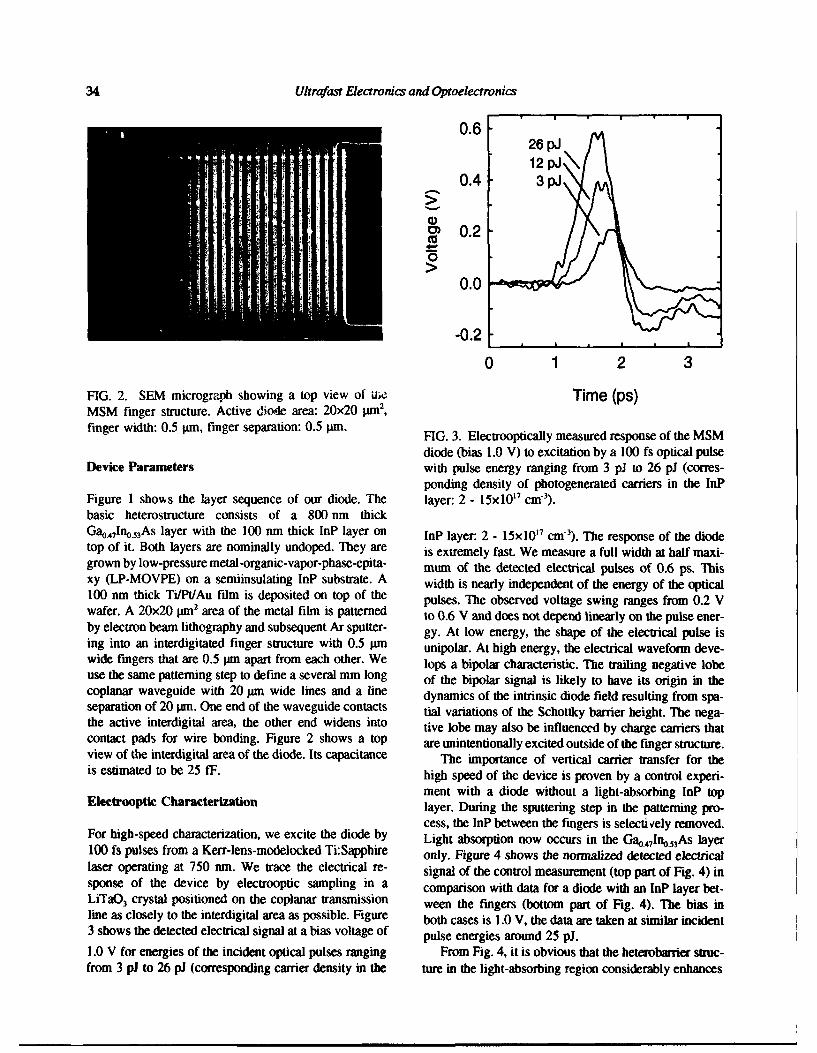
34 Ultrafast Electronics and Optoelectronics
0.626 pJ12pJ\
0.4 3 pJ>
4)S0.2W
0.0
-0.2 _,..._
0 1 2 3
FIG. 2. SEM micrograph showing a top view of UJe Time (ps)MSM finger structure. Active d.iode area: 20x20 pm2,finger width: 0.5 pim, finger separation: 0.5 gm. FIG. 3. Electrooptically measured response of the MSM
diode (bias 1.0 V) to excitation by a 100 fs optical pulseDevice Parameters with pulse energy ranging from 3 pJ to 26 pJ (corres-
ponding density of photogenerated carriers in the InPFigure 1 shows the layer sequence of our diode. The layer: 2 - 15x 10i7 cm 3).basic heterostructure consists of a 800 nm thickGa0471n0,. 3As layer with the 100 nm thick InP layer on InP layer: 2 - 15x1017 cm 3). The response of the diodetop of it. Both layers are nominally undoped. They are is extremely fast. We measure a full width at half maxi-grown by low-pressure metal-organic-vapor-phase-epita- mum of the detected electrical pulses of 0.6 ps. Thisxy (LP-MOVPE) on a semiinsulating InP substrate. A width is nearly independent of the energy of the optical100 rim thick Ti/Pt/Au film is deposited on top of the pulses. The observed voltage swing ranges from 0.2 Vwafer. A 20x20 pm 2 area of the metal film is patterned to 0.6 V and does not depend linearly on the pulse ener-by electron beam lithography and subsequent Ar sputter- gy. At low energy, the shape of the electrical pulse ising into an interdigitated finger structure with 0.5 Pm unipolar. At high energy, the electrical waveform deve-wide fingers that are 0.5 pm apart from each other. We lops a bipolar characteristic. The trailing negative lobeuse the same patterning step to define a several mm long of the bipolar signal is likely to have its origin in thecoplanar waveguide with 20 pm wide lines and a line dynamics of the intrinsic diode field resulting from spa-separation of 20 pmo. One end of the waveguide contacts tial variations of the Schottky barrier height. The nega-the active interdigital area, the other end widens into tive lobe may also be influenced by charge carriers thatcontact pads for wire bonding. Figure 2 shows a top are unintentionally excited outside of the finger structure.view of the interdigital area of the diode. Its capacitance The importance of vertical carrier transfer for theis estimated to be 25 MF. high speed of the device is proven by a control experi-
ment with a diode without a light-absorbing InP topElectrooptic Characterization layer. During the sputtering step in the patterning pro-
cess, the InP between the fingers is selecti rely removed.For high-speed characterization, we excite the diode by Light absorption now occurs in the Gao4 71n0o5 As layer100 fs pulses from a Kerr-lens-modelocked Ti:Sapphire only. Figure 4 shows the normalized detected electricallaser operating at 750 un. We trace the electrical re- signal of the control measurement (top part of Fig. 4) insponse of the device by electrooptic sampling in a comparison with data for a diode with an InP layer bet-LiTaO3 crystal positioned on the coplanar transmission ween the fingers (bottom part of Fig. 4). The bias inline as closely to the interdigital area as possible. Figure both cases is 1.0 V, the data are taken at similar incident3 shows the detected electrical signal at a bias voltage of pulse energies around 25 pJ.
1.0 V for energies of the incident optical pulses ranging From Fig. 4, it is obvious that the heterobarrier struc-from 3 pJ to 26 pJ (corresponding carrier density in the ture in the light-absorbing region considerably enhances
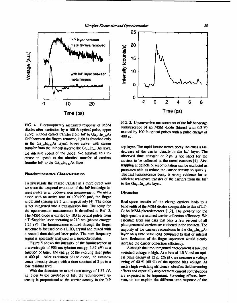
Ultrafast Electronics and Optoelectronics 35S25
,25InP layer between
metal fineiers removed .- 20
0 1• 10
with InP layer between Cmetal fingers
p~0*
0 10 20 -2 0 2 4 6 8
Time (ps) Time (ps)
FIG. 5. Upconversion measurement of the InP bandedgeFIG. 4. Electrooptically measured response of MSM luminescence of an MSM diode (biased with 0.2 V)
diodes after excitation by a 100 fs optical pulse, upper excited by 100 fs optical pulses with a pulse energy of
curve: without carrier transfer from InP to Gao47Ino 53As 400 pu.
(InP between the fingers removed, light is absorbed only
in the Gao0 47Ino53As layer), lower curve: with carriertransfer from the lnP cap layer to the GaO47Ino53As layer. top layer. The rapid luminescence decay indicates a fastthe intrinsic speed of the diode. We attribute this in- decrease of the carrier density in the IL? layer. The
crease in speed to the ultrafast transfer of carriers observed time constant of 2 ps is too short for the
fromthe InP to the Gao47Ino.53As layer. carriers to be collected at the metal contacts [4]. Alsotrapping at defects or recombination can be excluded asprocesses able to reduce the carrier density so quickly.
Photoluminescence Characterization The fast luminescence decay is strong evidence for anefficient real-space transfer of the carriers from the InP
To investigate the charge transfer in a more direct way to the Gao47InO. 53As layer.we trace the temporal evolution of the InP bandedge lu-minescence in an upconversion measurement. We use a Discussiondiode with an active area of 100xl00 pm2, the fingerwidth and spacing are 3 pm, respectively [4]. The diode Real-space transfer of the charge carriers leads to ais not integrated into a transmission line. The setup for bandwidth of the MSM diodes comparable to that of LT-the upconversion measurement is described in Ref. 5. GaAs MSM-photodetectors [1,2]. The penalty for theThe MSM diode is excited by 100 fs optical pulses from high speed is a reduced carrier collection efficiency. Wea Ti:Sapphire laser operating at 710 nm (photon energy: calculate from our data that only a few percent of all1.75 eV). The luminescence emitted through the finger photogenerated carriers are collected in the contacts. Thestructure is focused onto a LiUO 3 crystal and mixed with majority of the carriers recombines in the Ga0 47Ino.53Asa second time-delayed laser pulse. The sum frequency layer on a time scale long compared to that of interestsignal is spectrally analyzed in a monochromator. here. Reduction of the finger separation would clearly
Figure 5 shows the intensity of the luminescence at increase the carrier collection efficiency.a wavelength of 906 nm (photon energy: 1.37 eV) as a Although the time-integrated photocurrent is low, thefunction of time. The energy of the exciting laser pulse switched voltage is high. At a bias of 1.0 V and an opti-is 400 pJ. After excitation of the diode, the lumines- cal pulse energy of 12 pJ (26 pJ), we measure a voltagecence intensity decays with a time constant of 2 ps to a 3wing of 40 % (60 %) of the applied bias voltage. Atlow residual level. such a high switching efficiency, ultrafast field screening
With the detection set to a photon energy of 1.37 eV, effects and especially displacement current contributionsi.e. close to the bandedge of InP, the luminescence in- are expected to be important. Screening effects, how-tensity is proportional to the carrier density in the InP ever, do not explain the different time response of the
36 Utm~fast Ekaronics and Optoeleecrmnics
MSM diodes with and without InP layer between the made possible by financial support from the Deutschemetal fingers (see Fig. 4). We expect effective field Forschungsgemeinschaft.screening also when charee carriers are photogeneratedexclusively in the Gao.47Ino0 3As layer. Screening effects Referencescertainly influence the shape of the electric pulsesgenerated in both diode types and will have to be 1. S. Y. Chou, Y. Liu, W. Khalil, T. Y. Hsiang, and S.included in future model calculations. Alexandrou, Appl. Phys. Lea. 61 (1992) 819.
Conclusion 2. Y. Chen, S. Williamson. T. Brock, F. W. Smith, andA. R. Calawa, Appl. Phys. Lett. 59 (1991) 1984.
In summary, we have demonstrated that heterostruc-ture InP/GaOA7IDno 3As MSM-diodes are extremely fast 3. R. Kersting, X. Q. Thou, K. Wolter, D. Grilzimacher,photodetectors for photon energies above the bandgap of and H. Kurz, Superlan. Microstruc. 7 (1990) 345; andInP. Our experiments show that the observed subpicose- R. Kersting, R. Schwedler, K. Leo, and H. Kurz, incond response of the diodes results from an extremely Proc. 4th Int. Conf on InP and Related Materials,fast carrier trapping process in the form of a transfer of Newport, RI (1992) 565.carriers from the InP layer into the Gao47Ino.53As layer.The switched voltage is very high. The carrier collection 4. The increase of the active area of the diode used forefficiency is modest but can be improved by a reduction the upconversion experiment brings the advantage ofof the finger separation. For applications in the visible a higher luminescence intensity without increase ofand near-infrared spectral range (X < 900 nm), if speed the density of the photogenerated carriers. The largeris more important than quantum efficiency, this device spacing of the fingers raises the transit time formay be an interesting alternative to other ultrafast photo- electrons to reach the metal contacts to more thandetectors. 15 ps.
5. R. Kersting, K. Leo, J. Plettner, S. Averin, and H."Permanent address: Institute of Radioengineering and Kurz, in these Proceedings; see also R. Kersting, J.
Electronics, Square Academician Vvedensky 1, 141120 Plettner, K. Leo, S. Averin, and H. Kurz, Appl. Phys.Frjazino, Moscow, CIS. The stay at Aachen has been Lett., scheduled for publication in Febr. 1993.
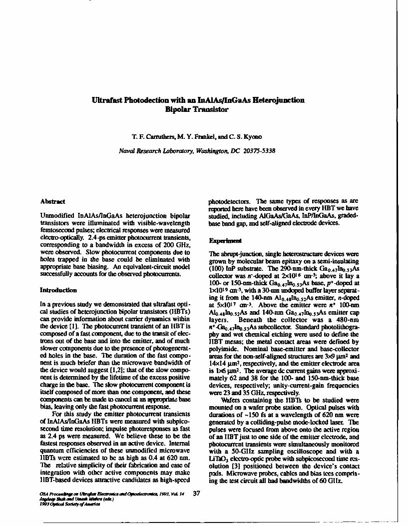
Ultrafast Photodection with an InAUIAs GaAs HeterojunctionBipolar Transistor
T. F. Carruthers, M. Y. Frankel, and C. S. Kyono
Naval Research Laboratory, Washington, DC 20375-5338
Abstract photodetectors. The same types of responses as arereported here have been observed in every HBT we have
Unmodified InAMAs/InGaAs heterojunction bipolar studied, including AIGaAs/GaAs, InP/InGaAs, graded-transistors were illuminated with visible-wavelength base band gap, and self-aligned electrode devices.femtosecond pulses; electrical responses were measuredelectro-optically. 2.4-ps emitter photocurrent transients,corresponding to a bandwidth in excess of 200 GHz,were observed. Slow photocurrent components due to The abrupt-junction, single heterostructure devices wereholes trapped in the base could be eliminated with grown by molecular beam epitaxy on a semi-insulatingappropriate base biasing. An equivalent-circuit model (100) lnP substrate. The 290-nm-thick Ga0 .4 7 1n0.5 3Assuccessfully accounts for the observed photocurrent•. collector was n-doped at 2x10 16
wn- above it lay a100- or 150-nim-thick Ga0 . 4 71n0 .5 3 As base, p÷-doped at
Introduction 1×x1 9 on-3, with a 30-nm undoped buffer layer separat-ing it from the 140-nim AI0.48In0. 5 2 As emitter, n-doped
In a previous study we demonstrated that ultrafast opti- at 5x10' 7 CM- 3. Above the emitter were n+ 100-nimcal studies of heterojunction bipolar transistors (IIBTs) Al. 41slno. 52As and 140-nm Ga0 .471n0. 53As emitter capcan provide information about carrier dynamics within layers. Beneath the collector was a 480-nmthe device [1]. The photocurrent transient of an ItBT is n÷4Ga0 .47 1n0. 5 3As subcollector. Standard photolithogra-composed of a fast component, due to the transit of elec- phy and wet chemical etching were used to define thetrons out of the base and into the emitter, and of much IIBT mesas; the metal contact areas were defined byslower components due to the presence of photogenerat- polyimide. Nominal base-emitter and base-collectored holes in the base. The duration of the fast compo- areas for the non-self-aligned structures are 3)0 lum2 andnent is much briefer than the microwave bandwidth of 14x14 ;Ln
2, respectively, and the emitter electrode areathe device would suggest [1,21; that of the slow compo- is 16 pm2 . The average dc current gains were approxi-nent is determined by the lifetime of the excess positive mately 62 and 38 for the 100- and 150-nm-thick basecharge in the base. The slow photocurrent component is devices, respectively; unity-current-gain frequenciesitself composed of more than one component, and these were 23 and 35 GHz, respectively.components can be made to cancel at an apprpriate base Wafers containing the lIBTs to be studied werebias, leaving only the fast photocurrent response. mounted on a wafer probe station. Optical pulses with
For this study the emitter photocurrent transients durations of -150 fs at a wavelength of 620 nm wereof InAlAs/InGaAs HBTs were measured with subpico- generated by a colliding-pulse mode-locked lasec Thesecond time resolution; impulse photoresponses as fast pulses were focused from above onto the active regionas 2.4 ps were measured. We believe these to be the of an IIBT just to one side of the emitter electrode, andfastest responses observed in an active device. Internal photocurrent transients were simultaneously monitoredquantum efficiencies of these unmodificd microwave with a 50-GIlz sampling oscilloscope and with aIIBTs wcre estimated to be as high as 0.4 at 620 nm. LiTaO3 electro-optic probe with subpicosecond time rcs-"lhe relative simplicity of their fabrication and case of olution [3] positioned between the device's contactintegration with other active componcnts may make pads. Microwave probes, cables and bias tccs compris-I IBT-based devices attractive candidates as high-speed ing the test circuit all had bandwidths of 60 GI lz.
0saProc*,ap on ouw tarotodeamtwiiz993, VoL 14 37Jq#&V Mk* and UtJh MIr. (ak)1993 OPtkd S0CWY CIeANi-~a
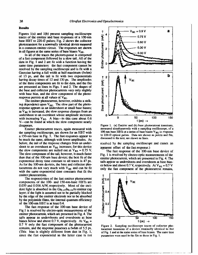
38 Ultrafast Electronics and Optoelectronics
Results
Figures 1(a) and 1(b) present sampling oscilloscope 4. VBE-0 9 V atraces of the emitter and base responses of a 100-nm 0.75 Vbase HBT to 220-f0 pulses; Fig. 2 shows the collectorphototransient for a nominally identical device meastured 0.60 V
in a common-emitter circuit. The responses are shown 2 0.30 Vin all figures at the same series of base biases VBE. 0.00 V
In all of the traces the photoresponse is composed 0of a fast component followed by a slow tail. All of thedata in Fig. 1 and 2 are fit with a function having the - 0 -
same time parameters: the fast component cannot be EtJJresolved by the sampling oscilloscope and is fit with a _
Gaussian having a full width at half-maximum (fwhm)of 13 ps, and the tail is fit with two exponentials 1 2 A bhaving decay times of 12 and 130 ps. The amplitudes VBEof the three components are fit to the data, and the fitsare presented as lines in Figs. 1 and 2. The shapes of
the base and collector photocurrents vary only slightlywith base bias, and the slow component of the photo- "response persists at all values of VBE. 0
The emitter photocurrent, however, exhibits a strik-ing dependence upon VBE. The slow part of the photo-response appears as an undershoot at small base biases;as V BE is increased, the slow response changes from an m
undershoot to an overshoot whose amplitude increases 0with increasing VBE. A bias-in this case about 0.6 0 50 100 150V-can be found at which the slow component nearly t (ps) -4
disappears. Figure 1. (a) Emitter and (b) base photocurrent transients,Emitter photocurrent traces, again measured with measured simultaneously with a sampling oscilloscope, of a
the sampling oscilloscope, are shown for an HBT with 100-nm base IlBTs at a series of base biases VBE in responsea 150-nm base in Fig. 3. The fast responses appear to to 220-f0 optical pulses. Data are shown as points and fits,be much the same, although with lower amplitudes. As discussed in the text, are shown as lines.
before, the tail of the respoase changes from an under- resolved by the sampling oscilloscope and causes anshoot to an overshoot as VBE increases; for this device apparent offset of the fast response.)the slow components are nulled out at VBE = 0.75 V. The fast response of the 100-nm base device ofThe slow component of the tail, however, is much faster Fig. I is resolved by electro-optic measurements of thethan that of the 100-nm base device; the best fit of the emitter photocurrent, which are presented in Fig. 4. Theexponential decay time constant to all traces is 47 ps. tails appear as undershoots and overshoots at base bias-As for the 100-rnm devices, the base and collector pho- es below and above 0.7 V, respectively. At V BE = 0.7 Vtocurrents do not vary much with VBE and can be fit only the fast component of the photocurrent remains,with the same exponential time constants that fit theemitter photocurrents.
The rcsponsivities of the fast emitter photocurrent ;Z0.6components of the 100- and 150-nm-base IIBTs are E. VB0.039 and 0.016 A/W, respectively. Most of the inci-dent light is absorbed in the Ga0 .47In 0.53As emitter caplayer; if the light is assumed not to be partially blocked • 0.4
by the edge of the emitter electrode nor to be absorbed Vby the polyimide films, the internal quantum efficiency Rof the 100-nm I IBT is at least 0.4. 002
The fast response of the 100-nm base device ofFig.1 is resolved by electro-optic measurements of theemitter photocurrent, which are presented in Fig. 4. The 0tails appear as undershoots and overshoots at base - 0 50 100 150biases below and above 0.7 V, respectively. At VBE = t (ps)0.7 V only the fast component of the photocurrent Figure 2. Sampling oscilloscope traces of collector pho-remains, and the response possesses a fwhm of 5.5 ps. tocurrent transients of a device nominally identical to that(This bias is slightly different from that in Fig. 1, of Fig. I and at the same series of base biases. The same timesince the fast exponential in the latter case is not parameters were used in the fits as those in Fig. 1.
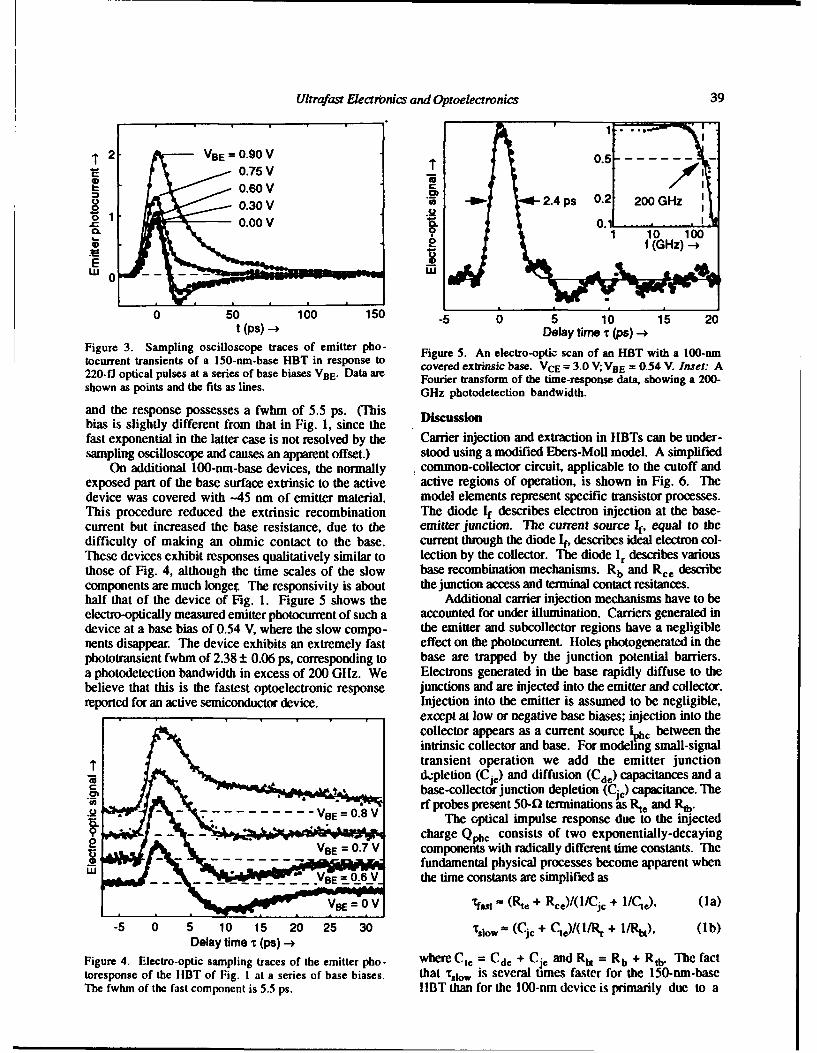
Ultrafast Electrmnics and Optoelectronics 39
2- VBE 0.90 V 0.5:- -- -- - ----0.75 V0.60 V
0.' ~2.4ps 0.2 200GHzS0.30 V K20. . .0~ 1 AA.4.0oV 200 G 1
0.0 0.S0. 9 1 10 10
t (ps • Dlay ime f ( GpsE
0 50 100 150 -5 0 5 10 15 20t (PS) -4 Delay tirme T (ps) -4
Figure 3. Sampling oscilloscope traces of emitter pho- Figure 5. An electro-optic scan of an HBT with a 100-nmtocurrent transients of a 150-rn-base HBT in response to covered extrinsic base. VCE = 3.0 V; VBE = 0.54 V. Inset: A220-fi optical pulses at a series of base biases VBE. Data are Fourier transform of the time-response data, showing a 200-shown as points and the fits as lines. GHz photodetection bandwidth.
and the response possesses a fwhm of 5.5 ps. (This Discussionbias is slightly different from that in Fig. 1, since thefast exponential in the latter case is not resolved by the Carrier injection and extraction in HBTs can be under-sampling oscilloscope and causes an apparent offset.) stood using a modified Ebers-Moil model. A simplified
On additional 100-rim-base devices, the normally common-collector circuit, applicable to the cutoff andexposed part of the base surface extrinsic to the active active regions of operation, is shown in Fig. 6. Thedevice was covered with -45 nm of emitter material, model elements represent specific transistor processes.This procedure reduced the extrinsic recombination The diode If describes electron injection at the base-current but increased the base resistance, due to the emitter junction. The current source If, equal to thedifficulty of making an ohmic contact to the base. current through the diode If, describes ideal electron col-These devices exhibit responses qualitatively similar to lection by the collector. The diode 1r describes variousthose of Fig. 4, although the time scales of the slow base recombination mechanisms. Rb and Rce describecomponents are much longec The responsivity is about the junction access and terminal contact resitances.half that of the device of Fig. 1. Figure 5 shows the Additional carrier injection mechanisms have to beelectro-optically measured emitter photocurrent of such a accounted for under illumination. Carriers generated indevice at a base bias of 0.54 V, where the slow compo- the emitter and subcollector regions have a negligiblenents disappear. The device exhibits an extremely fast effect on the photocurrent. Holes photogenerated in thephototransient fwhm of 2.38 ± 0.06 ps, corresponding to base are trapped by the junction potential barriers.a photodetection bandwidth in excess of 200 Gllz. We Electrons generated in the base rapidly diffuse to thebelieve that this is the fastest optoelectronic response junctions and are injected into the emitter and collector.reported for an active semiconductor device. Injection into the emitter is assumed to be negligible,
except at low or negative base biases; injection into thecollector appears as a current source Iphc between theintrinsic collector and base. For modeling small-signaltransient operation we add the emitter junction--depletion (Cje) and diffusion (Cde) capacitances and abase-collector junction depletion (Cjc) capacitance. TIerf probes present 50-41 terminations as Rt. and Rtb.
.9• 7.-VBE - 0.8 VThe optical impulse response due to the injected0.charge QPhc consists of two exponentially-decaying
VBE = 0.7 V components with radically different time constants. The-- - - - - fundamental physical processes become apparent when
-=06V the time constants are simplified as% (Rte + Rce)/(lICjc + 1/ 1 d, (la)
-5 0 5 10 15 20 25 30 (Ci. + Cq.)/(i/Rt + I/R%), (lb)Delay time T (ps) -4
Figure 4. Electro-optic sampling traces of the emitter pho- where C,, = Cde + Cje and Rl, = Rb +Rtb. The facttoresponse of the ilBT of Fig. I at a series of base biases. that Tslow is several times faster for the 150-nm-baseThe fwhm of the fast component is 5.5 ps. IIBT than for the 100-nim device is primarily due to a
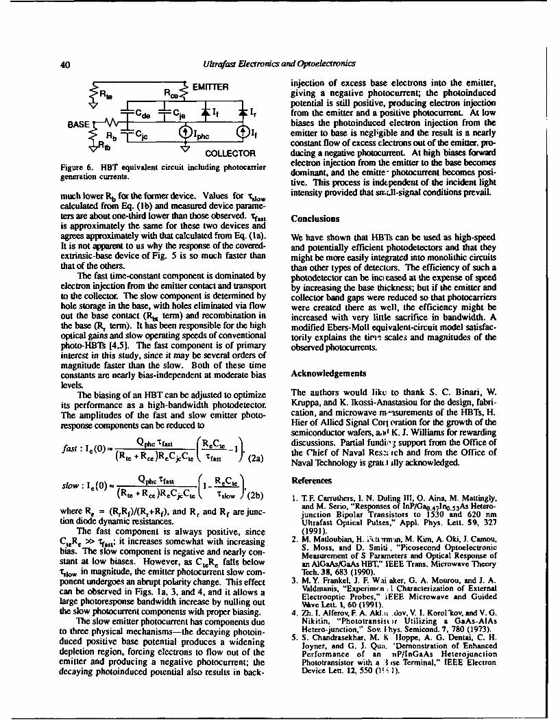
40 Ultrafast Electronics and Oproelectronics
SEMITTER injection of excess base electrons into the emitter,Rig Rgiving a negative photocurrent; the photoinduced
. _E I potential is still positive, producing electron injectionCde Cie It Ir from the emitter and a positive photocurrent. At low
BASE _JR: (biases the photoinduced electron injection from the-Rb Cc jIphc + if emitter to base is negligible and the result is a nearly
constant flow of excess electrons out of the emitter. pro-COLLECTOR ducing a negative photocurrent. At high biases forward
Figure 6. HBT equivalent circuit including photocarrier electron injection from the emitter to the base becomes
generation currents. dominant, and the emitte- photocurrent becomes posi-tive. This process is independent of the incident light
much lower Rb for the former device. Values for %slw intensity provided that snfll-signal conditions prevaiL
calculated from Eq. (lb) and measured device parame-ters are about one-third lower than those observed. tfst Conclusionsis approximately the same for these two devices andagrees approximately with that calculated from Eq. (Ia). We have shown that HBTs can be used as high-speedIt is not apparent to us why the response of the covered- and potentially efficient photodetectors and that theyextrinsic-base device of Fig. 5 is so much faster than might be more easily integrated into monolithic circuitsthat of the others. than other types of detectors. The efficiency of such a
The fast time-constant component is dominated by photodetector can be inc reased at the expense of speedelectron injection from the emitter contact and transport by increasing the base thickness; but if the emitter andto the collector. The slow component is determined by collector band gaps were reduced so that photocarriershole storage in the base, with holes eliminated via flow were created there as well, the efficiency might beout the base contact (R% term) and recombination in increased with very little sacrifice in bandwidth. Athe base (Rr term). It has been responsible for the high modified Ebers-Moll equivalent-circuit model satisfac-optical gains and slow operating speeds of conventional torily explains the tirv. scales and magnitudes of thephoto-HBTs [4,5]. The fast component is of primary observed photocurnents.interest in this study, since it may be several orders ofmagnitude faster than the slow. Both of these timeconstants are nearly bias-independent at moderate bias Acknowledgementslevels.
The biasing of an HBT can be adjusted to optimize The authors would likte to thank S. C. Binari, W.its performance as a high-bandwidth photodetector. Kruppa, and K. Ikossi-Anastasiou for the design, fabri-The amplitudes of the fast and slow emitter photo- cation, and microwave mi-tsurements of the HBTs, H.
response components can be reduced to Hier of Allied Signal Cot oration for the growth of thesemiconductor wafers, aad K. J. Williams for rewarding
fas : (I discussions. Partial fundii-7 support from the Office offatc Cfs 'Re jt 1 a, the Chief of Naval Res-- Ich and from the Office offas:(O.(Rt + R)RCc fas (2a) Naval Technology is grat.! illy acknowledged.
Qphc 'fast Ii R.eCte Referencesslo : e(0 ==(R ,e + Rce)R .C ic~te T,- s- 0-w )(bslo + 1.)e~ t (0)ie )'(2b) 1. T F. Carruthers, I. N. Duling 111, 0. Aina, M. Mattingly,
and M. Serio, "Responses of lnP/Gao.47In0.53As Hetero-where R, = (RrRf)/(Rr+Rf), and R, and R f arejunc- junction Bipolar Transistors to 1530 and 620 nmtion diode dynamic resistances. Ultrafast Optical Pulses." Appl. Phys. Lett. 59, 327
The fast component is always positive, since (1991).CteRe >> T.ast; it increases somewhat with increasing 2. M. Matloubian, H. !ktt'rmrAn, M. Kim, A. Ok, J. Camou,bias. The slow component is negative and nearly con- S. Moss, and D. Smiti, "Picosecond Optoelectronic
Measurement of S Parameters and Optical Response ofstant at low biases. However, as CteRe falls below an AIGaAs/GaAs HBT," IEEE Trans. Microwave Theory
silow in magnitude, the emitter photocurrent slow coin- Tech. 38, 683 (1990).ponent undergoes an abrupt polarity change. This effect 3. M. Y. Frankel, J. F. Wai aker, G. A. Mourou, and J. A.can be observed in Figs. la, 3, and 4, and it allows a Valdmanis, "Experimc.n ; I Characterization of External
Electrooptic Probes," iEEE Microwave and Guidedlarge photoresponse bandwidth increase by nulling out %•ve Lett. 1, 60 (1991).the slow photocurrent components with proper biasing. 4. Zh. I. Alferov, F. A. Akl.m dov, V. I. Korol'kov, and V. G.
The slow emitter photocurrent has components due Nikitin, "Phototransist)r Utilizing a GaAs-AlAsto three physical mechanisms-the decaying photoin- Hetero-junction," Soy. t'hys. Semicond. 7, 780 (1973).duced positive base potential produces a widening 5. S. Chandrasekhar, M. K Iloppe, A. G. Dentai, C. H.
Joyner, and G. J. Qua. 'Demonstration of Enhanceddepletion region, forcing electrons to flow out of the Performance of an nP/lnGaAs Heterojunctionemitter and producing a negative photocurrent; the Phototransistor with a 3 tse Terminal," IEEE Electrondecaying photoinduced potential also results in back- Device Len. 12, 550 (1' i 1).
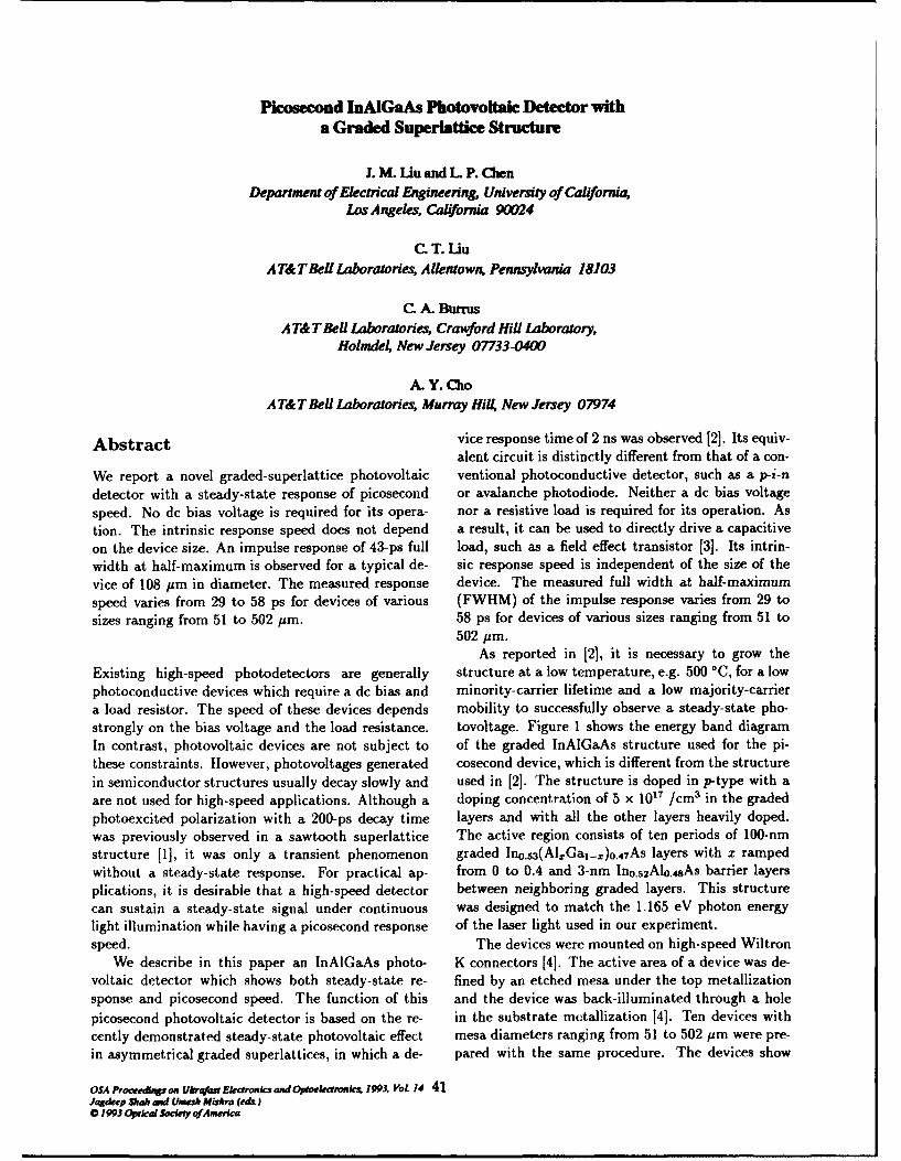
Picosecond InAIGaAs Photovoltaic Detector witha Graded Superlattice Structure
L M. Liu and L P. Chen
Department of Electrical Engineering, University of Caifornia,Los Angeles, California 9(024
C. T. LiuA T& TBell Laboratories, Allentown, Pennsylvania 18103
C. A. Burrus
A T& T Bell Laboratories, Crawford Hill Laboratory,Holmdel, New Jersey 07733-0400
A. Y. ChoA T& T Bel Laboratories, Murray HRl New Jersey 07974
Abstract vice response time of 2 ns was observed 12]. Its equiv-alent circuit is distinctly different from that of a con-
We report a novel graded-superlattice photovoltaic ventional photoconductive detector, such as a p-i-ndetector with a steady-state response of picosecond or avalanche photodiode. Neither a dc bias voltagespeed. No dc bias voltage is required for its opera- nor a resistive load is required for its operation. As
tion. The intrinsic response speed does not depend a result, it can be used to directly drive a capacitiveon the device size. An impulse response of 43-ps full load, such as a field effect transistor [3]. Its intrin-width at half-maximum is observed for a typical de- sic response speed is independent of the size of thevice of 108 pm in diameter. The measured response device. The measured full width at half-maximumspeed varies from 29 to 58 ps for devices of various (FWHM) of the impulse response varies from 29 tosizes ranging from 51 to 502 pm. 58 ps for devices of various sizes ranging from 51 to
502 pm.As reported in [2], it is necessary to grow the
Existing high-speed photodetectors are generally structure at a low temperature, e.g. 500 0C, for a lowphotoconductive devices which require a dc bias and minority-carrier lifetime and a low majority-carriera load resistor. The speed of these devices depends mobility to successfully observe a steady-state pho-strongly on the bias voltage and the load resistance. tovoltage. Figure 1 shows the energy band diagramIn contrast, photovoltaic devices are not subject to of the graded InAlGaAs structure used for the pi-these constraints. However, photovoltages generated cosecond device, which is different from the structurein semiconductor structures usually decay slowly and used in [2]. The structure is doped in p-type with aare not used for high-speed applications. Although a doping concentration of 5 x 10" /cm' in the gradedphotoexcited polarization with a 200-ps decay time layers and with all the other layers heavily doped.was previously observed in a sawtooth superlattice The active region consists of ten periods of 100-nmstructure [1], it was only a transient phenomenon graded Ino.s3(AlxGa-x)0.4 7As layers with x rampedwithout a steady-state response. For practical ap- from 0 to 0.4 and 3-nm Ino.s2 A60.4As barrier layersplications, it is desirable that a high-speed detector between neighboring graded layers. This structurecan sustain a steady-state signal under continuous was designed to match the 1.165 eV photon energylight illumination while having a picosecond response of the laser light used in our experiment.speed. The devices were mounted on high-speed Wiltron
We describe in this paper an lnAlGaAs photo- K connectors [4]. The active area of a device was de-voltaic detector which shows both steady-state re- fined by an etched mesa under the top metallizationsponse and picosecond speed. The function of this and the device was back-illuminated through a holepicosecond photovoltaic detector is based on the re- in the substrate metallization [4]. Ten devices withcently demonstrated steady-state photovoltaic effect mesa diameters ranging from 51 to 502 pm were pre-in asymmetrical graded superlattices, in which a de- pared with the same procedure. The devices show
OSA Prod on Ublo/nu Eleceronks ald Optoewkonics 1993. VoL 14 41Jqdeep SWh d Umesh Mrhra (edL)0 1993 Opdca Sockry ofAmerica
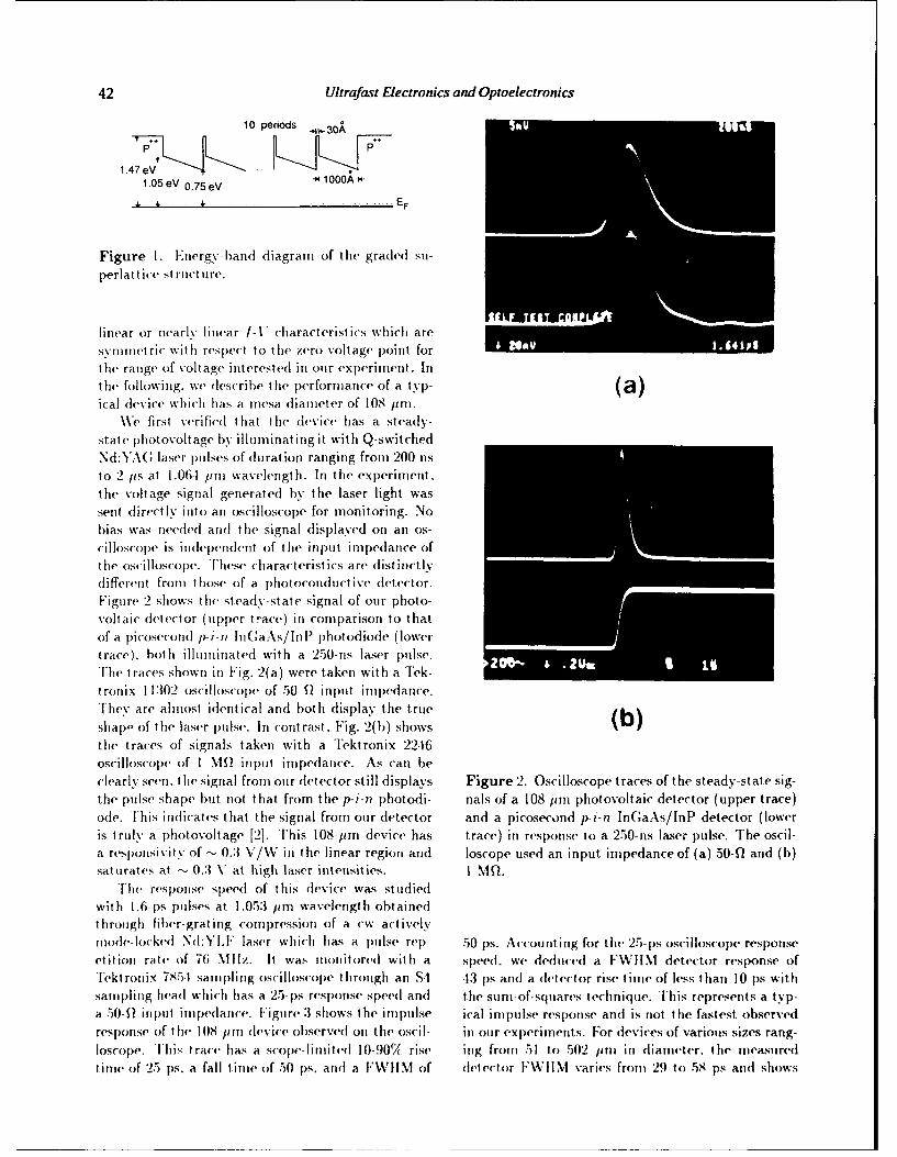
42 Ultrafast Electronics and Optoelectronics
10 periods -i-30A
1.47 eV1.05eV 0.75eV 1000A
k •- ... . .. .. ... . ... ... ... E F
Figure 1. Energy-hIand diagram of the graded su-
perlat t ice st ruct tire.
linear or nearly linear /-V characteristics which aresyinnietric with respect to the zero voltage point forthe range of voltage interested in our experiment. hithe following, we dtescrib)e thlie performiance of a tyvp- (a)ical device which has a mesa diameter of 108 pin.
We first verified that thlie device has a steady-
state pihotovoltage by illuminatingit with Q-switchedNd:YA(; laser pulses of durat ion ranging from 200 nsto 2 ps at 1.06.1 pmi wavelength. In the experiment.
the voltage signal generated by the laser light wassent directly, into an oscilloscope for monitoring. Nobias was needed and the signal displayed on an os-
cilloscope is independent of the input impedance of
the oscilloscope. These characteristics are distinctlydifferent from those of a phiotoconductive detector.Figure 2 shows the steady-state signal of our photo-
voltaic detector (upper trace) in comparison to thatof a picosecond p-i-n in.aAs/InP photodiode (lower
trace), both illuminated with a 250-nis laser pulse.
The traces shown in Fig. 2(a) were taken with a Tek-tronix 11302 oscilloscope of 50 Q input impedance.
They are almost identical and both display the true
shape of the laser pulse. In contrast. Fig. 2(b) shows
the traces of signals taken with a Tektronix 2216oscilloscope of I .1!' input impedance. As can be
clearly seen. the signal from our detector still displays Figure 2. Oscilloscope traces of the steady-state sig-
the pulse shape but not that from the p-i-n photodi- nals of a 108 pin photovoltaic detector (upper trace)ode. ]ihis indicates that the signal from our detector and a picosecond p-i-n InGaAs/InP detector (lower
is truly a photovoltage [2]. This 108-pmr device has trace) in response to a 2Y50-ns laser pulse. The oscil-
a responsivitv of -, 0.3 V/W in the linear region ard loscope used an input impedance of (a) 50-Q and (b)
saturates at - 0.3 V at hight laser intensities. I MQI.
"Ihe response speed of tihis device was studiedwith 1.6-ps pulses at 1.05:1 pim wavelength obtainedthrough fiber-grating comp)ression of a cw activelymode-locked N(:YIF laser which has a pulse rep- 50 ps. Accounting for the 25-ps oscilloscope responseetition rate of 76 Mlxz. It was mlonitored with a speed, we deduced a FWIIM detector response of
Tektronix 7854 sampling oscilloscope through an S4 -13 ps and a detector rise time of less than 10 ps with
sampling head which has a 25-ps response speed and the suuni-of-squares technique. This represents a typ-
a 50-f innput imnpedlance. Figure :1 shows the impulse ical imppulse response and is riot the fastest observed
response of the 108 pmi device observed on the oscil- in our experiments. For devices of various sizes rang-
loscope. This trace has a sCOpue-limnited 10-.90(X rise ing front 51 to 502 pm in diameter, the measured
imne of 2.5 ps. a fall timne of 50 ps. and a |WIIM of detector FWIIM varies fronm 29 to 58 ps and shows
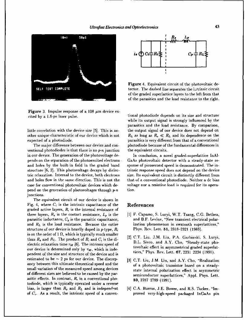
Ultrafast Electronics and Optoelectronics 43
11R 8 LP
isLcT RJi Cp RL
VW Figure 4. Equivalent circuit of the photovoltaic de-SELF TST COPLETEtector. The dashed line separates the iitrinsic circuit
of the graded superlattice layers to the left from thatof the parasitics and the load resistance to the right.
Figure 3. Impulse response of a 108 pm device ex-cited by a 1.6-ps laser pulse. tional photodiode depends on its size and structure
while its output signal is strongly influenced by theparasitics and the load resistance. By comparison,
little correlation with the device size [5]. This is an- the output signal of our device does not depend onother unique characteristic of our device which is not RL as long as R,< RL. and its dependence on theexpected of a photodiode. parasitics is very different from that of a conventional
The major difference between our device and con- photodiode because of the fundamental differences inventional photodiodes is that there is no p-n junction the equivalent circuits.in our device. The generation of the photovoltage de- In conclusion, a novel graded-superlattice InAl-pends on the separation of the photoexcited electrons GaAs photovoltaic detector with a steady-state re-and holes by the built-in field in the graded band sponse of picosecond speed is demonstrated. The in-structure [6, 2]. This photovoltage decays by dielec- trinsic response speed does not depend on the devicetric relaxation. Internal to the device, both electrons size. Its equivalent circuit is distinctly different fromand holes flow in the same direction. This is not the that of a conventional photodiode. Neither a dc biascase for conventional photovoltaic devices which de- voltage nor a resistive load is required for its opera-pend on the generation of photovoltages through p-n tion.junctions.
The equivalent circuit of our device is shown inFig. 4, where C, is the intrinsic capacitance of the Referencesgraded active layers, R, is the internal resistance ofthese layers, R., is the contact resistance, LP is the [1] F. Capasso, S. Luryi, W.T. Tsang, C.G. Bethea,parasitic inductance, Cp is the parasitic capacitance, and B.F. Levine, "New transient electrical polar-and RL is the load resistance. Because the entire ization phenomenon in swatooth superlattices,"structure of our device is heavily doped in p-type, R, Phys. Rev. Lett. 51, 2318-2321 (1983).is on the order of 1 Q~, which is typically much smaller 2C. LuJM iPA.GrnsS.uy,
thanR, nd L- Te podut ofRi nd i isthedi- D.L. Sivco, and A.Y. Cho, "Steady-state pho-electric relaxation time TM [6]. The intrinsic speed of tovoltaic effect in asymmetrical graded superlat-our device is determined only by rM, which is inde- tcs"Py.Rv et 7 2123 19)pendent of the size and structure of the device and is tcs"Py.Rv et 7 2123 19)estimated to be '- 2 ps for our device. The discrep- [3] C.T. Liu, J.M. Liu, and A.Y. Cho, "Realizationancy between this ultimate theoretical speed and the of a photovoltaic transistor based on a steady-small variation of the measured speed among devices state internal polarization effect in asymmetricof different sizes are believed to be caused by the par- semiconductor superlattices," AppI. Phys. Lett.asitic effects. In contrast, Ri in a conventional pho- 59, 2787-~2789 (1991).todiode, which is typically operated under a reversebias, is larger than R, and RL and is independl~nt [4] C.A. Burrus, i.E. Bower, and R.S. Tucker, "Im-of Ci. As a result, the intrinsic speed of a conven- proved very-high-speed packaged InGaAs pin
44 Ultrafast Electronics and Optoelectronics
punch-through photodiode," Electron. Lett. 21, to Appl. Phys. Lett.262-263 (1985).
[5] J.M. Liu, L.P. Chen, C.T. Liu, C.A. Burrus, and 16] C.T. Liu and S. Luryi, "Photovoltaic transistorA.Y. Cho, "Picosecond response of steady-state based on a steady-state internal polarization ef-photovoltaic effect in an asymmetrical graded fect in asymmetric semiconductor superlattices,"semiconductor superlattice structure," submitted Appl. Phys. Lett. 59, 393-395 (1991).
100 GHz Double Heterostructure GaInAs/InPp-i-n Photodiode
Yih-Guei Wey, Kirk S. Giboney, John E. Bowers, andMark J. W. Rodwell
Department of Electrical and Computer Engineering University of California,Santa Barbar, California 93106
Pierre Silvestre, Prabhu Thiagrarajan, and Gary Y. RobinsonDepartment of Electrical Engineering, Colorado State University,
Fort Collins, Colorado 80523
Abstract bandwidths as large as 110 GHz are observed for a
We report double heterostructure GaInAs/InP p-i-n 2 pm x 2 jum device at low bias voltages.
photodiodes with pulsewidths as short as 3.0 ps, Materials & Fabricationbandwidths exceeding 100 GHz, and external quantumefficiency of 50%. The heterostructure shown in Figure 1 was grown by
Introduction gas-source molecular beam epitaxy at 500TC nominally
lattice matched to a (100) semi-insulating InP substrate.
High-speed, high efficiency photodetectors sensitive at Molecular beams of As2 and P2 were produced by
1.3 and 1.55 jim are vital components for the thermal decomposition of AsH3 and PH3 , and Be and
development of large-capacity digital and analog optical Si were used as dopants. One Ga effusion cell and two
fiber communications systems and instrumentation. In cells, one for InGaAs at 0.4 pm/hr and one forSuch photodetectors are generally subject to InGaAsP (Xg = 1.15 jIm) at 1.2 un/hr and InP at 1.0performance limitations such as carrier transit time, RC jum/hr, were used. This procedure ensured constant
time constant, diffusion current, and carrier trapping. alloy composition, precise layer thickness, and abrupt
Until now, high-speed long wavelength photodiodes heterointerfaces during growth of the graded bandgaphave had 3-dB bandwidths of no more than 70 GHz regions [4].
due to these limitations [1, 21. Our photodiode design The device cross-section is shown in Figure 2.utilizes a GaInAs/lnP p-i-n double heterostructure with Fabrication is described as follows. Ti(50 nm)/ Pt(75graded bandgap layers to reduce the heterojunction nm)/Au(150 nm)/Ni(100 nm) is lifted off on the wafer
barrier height and minimize carrier trapping at the with a tri-level mask technique. Thehetero-interfaces. An additional graded layer at the PMMA(1 jm)/Si(50 nm)/AZ4110(1 pim) ui-level maskp+GaInAs/pInP contact interface reduces the contact is first prepared by patterning the AZ41 10 resist on topresistance significantly over that of previously reported of Si and soft-baked PMMA. The silicon layer is
devices [2, 31. Leakage current and reverse breakdown etched by chlorine reactive ion etch (RIE) and thevoltage are also improved by replacing SiN, passivation PMMA (e-beam resist) is etched by oxygen RIE. The
with a self-aligned polyimide passivation. undercut of PMMA is formed by oxygen plasma in aA pump-probe electro-optic sampling system based plasma enhanced etching machine. The nickel layer
on a Ti:Sapphire laser allows direct measurement of the serves as etch mask for C!2 RIE mesa etch through the
ultrafast photodiode with subpicosecond resolution at intrinsic layer. The n-InP layer is defined by972 nm. Measured pulsewidths as short as 3.0 ps full- 1HCI:IH 2 0 wet etching with AZ4110 patternedwidth at half-maximum (FWHM), and 3-dB plasma-enhanced-chemical-vapor-deposition (PECVD)
osA Procmweqs#V o, u&ruf Ekamrt and Opvoekal'tmn 199.m voL 14 45Jegdeep SWk and Uuah Mikhra (edL)01993 (p.kd Socer ofAnerka
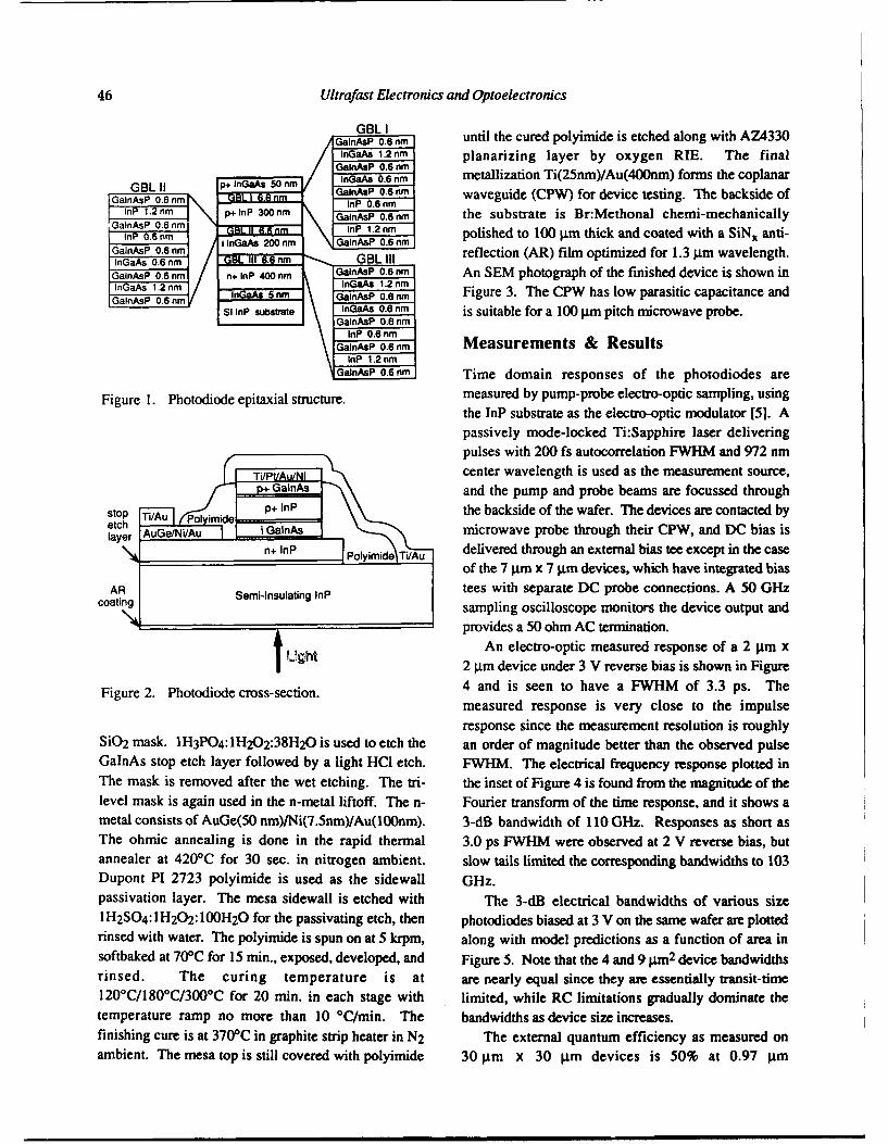
46 Ultrafast Electronics and OptoelectronicsGBLI
GalnAsP 0.6 nrm until the cured polyimide is etched along with AZ4330lnGaAs 1.2 nm planarizing layer by oxygen RIE. The finalGalnAsP 0.6 nm'
GBL 11 p+ tInGaAs 50 nm InGaAs 0.6 nm metallization Ti(25nm)/Au(400nm) forms the coplanarGalnAsP 0.6 nm GaInAsP 0.6 ,m waveguide (CPW) for device testing. The backside ofInP .2 n p+fnRN5nmInP 0.6 nm
InP 1.2 nm ptnp 300 rim GaInAsP 0.6 nm the substrate is Br:Methonal chemi-mechanicallyGaInsP 0.6 rnm WInP 1.2 nm polished to 100 prm thick and coated with a SiNx anti-
GaInGaAs 0.6nm/. nm GBL II reflection (AR) film optimized for 1.3 pim wavelength.
GaInAsP 0.6 nm n+ InP 400 nm GalnAsP 0.6 rm An SEM photograph of the finished device is shown inGanAsP m.2 nm GalAsP 0.6 nm Figure 3. The CPW has low parasitic capacitance and
SI InP substrate InGaft 0.6 nm is suitable for a 100 pm pitch microwave probe.~GaInAsP 0.6 nmInP 0.6 nmn
GaInAsP 0.6 nm Measurements & ResultsInP 1.2 nmA
GaInAsP 0.6 nm Time domain responses of the photodiodes are
Figure 1. Photodiode epitaxiaJ structure. measured by pump-probe electro-optic sampling, usingthe InP substrate as the electro-optic modulator [5]. Apassively mode-locked Ti:Sapphire laser deliveringpulses with 200 fs autocorrelation FWHM and 972 nm
Tt/Pt/Au/Ni "center wavelength is used as the measurement source,and the pump and probe beams are focussed through
stop T p+ InP the backside of the wafer. The devices are contacted by
layer AuGe/Ni/Au i GalnAs microwave probe through their CPW, and DC bias iso dn+ InP Ti/Au delivered through an external bias tee except in the caseof the 7 pnm x 7 prm devices, which have integrated bias
AR Semi-Insulating InP tees with separate DC probe connections. A 50 GHzcoating sampling oscilloscope monitors the device output and
provides a 50 ohm AC termination.Lg An electro-optic measured response of a 2 ptm xLght 2 pgm device under 3 V reverse bias is shown in Figure
Figure 2. Photodiode cross-section. 4 and is seen to have a FWHM of 3.3 ps. Themeasured response is very close to the impulseresponse since the measurement resolution is roughly
SiO2 mask. 1H3PO 4:1H 20 2:38H 20 is used to etch the an order of magnitude better than the observed pulseGaInAs stop etch layer followed by a light HCI etch. FWHM. The electrical frequency response plotted inThe mask is removed after the wet etching. The tri- the inset of Figure 4 is found from the magnitude of thelevel mask is again used in the n-metal liftoff. The n- Fourier transform of the time response, and it shows ametal consists of AuGe(50 nm)/Ni(7.5nm)/Au(100nm). 3-dB bandwidth of 110 GHz. Responses as short asThe ohmic annealing is done in the rapid thermal 3.0 ps FWHM were observed at 2 V reverse bias, butannealer at 420*C for 30 sec. in nitrogen ambient. slow tails limited the corresponding bandwidths to 103Dupont P1 2723 polyimide is used as the sidewall GHz.passivation layer. The mesa sidewall is etched with The 3-dB electrical bandwidths of various sizeI H2SO 4: 1 H20 2: I 00H20 for the passivating etch, then photodiodes biased at 3 V on the same wafer are plottedrinsed with water. The polyimide is spun on at 5 krpm, along with model predictions as a function of area insoftbaked at 70*C for 15 min., exposed, developed, and Figure 5. Note that the 4 and 9 prm2 device bandwidthsrinsed. The curing temperature is at are nearly equal since they are essentially transit-time120 0C/180°C/3000C for 20 min. in each stage with limited, while RC limitations gradually dominate thetemperature ramp no more than 10 0C/min. The bandwidths as device size increases.finishing cure is at 370 0C in graphite strip heater in N2 The external quantum efficiency as measured onambient. The mesa top is still covered with polyimide 30 pgm x 30 pgm devices is 50% at 0.97 pgm
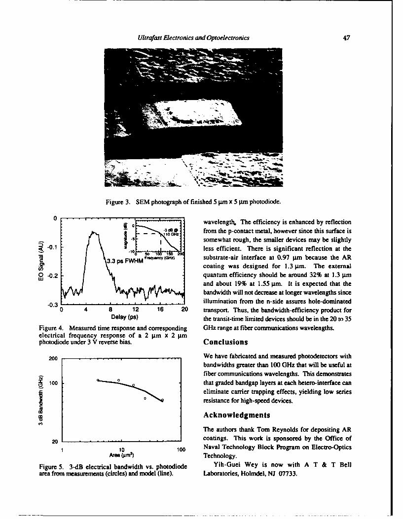
Ultrafast Electronics and Optoelectronics 47
h ,.
Figure 3. SEM photograph of finished 5 gim x 5 gm photodiode.
0 wavelength. The efficiency is enhanced by reflection3B@ 0 from the p-contact metal, however since this surface is
" ,somewhat rough, the smaller devices may be slightly
"-."o less efficient. There is significant reflection at the.1% so0oo1is
3.3 ps FWHMRUe- (Oz) substrate-air interface at 0.97 gm because the AR3.3 C. coating was designed for 1.3 pgm. The external
O -0.2 quantum efficiency should be around 32% at 1.3 gmw and about 19% at 1.55 gm. It is expected that thebandwidth will not decrease at longer wavelengths since
-0.3 illumination from the n-side assures hole-dominated0 4 8 12 16 20 transport. Thus, the bandwidth-efficiency product for
Delay (ps) the transit-time limited devices should be in the 20 to 35
Figure 4. Measured time response and corresponding GHz range at fiber communications wavelengths.electrical frequency response of a 2 g~m x 2 gimphotodiode under 3 V reverse bias. Conclusions
200 We have fabricated and measured photodetectors with
bandwidths greater than 100 GHz that will be useful atfiber communications wavelengths. This demonstrates
o100 0that graded bandgap layers at each hetero-interface caneliminate carrier trapping effects, yielding low seriesresistance for high-speed devices.
AcknowledgmentsThe authors thank Tom Reynolds for depositing AR
2 0 . . . . . . . .. . . . . . . . c o a tin g s . T h is w o rk is sp o n so red b y th e O ff ic e o f
1 10 100 Naval Technology Block Program on Electro-OpticsArea (pm2) Technology.
Figure 5. 3-dB electrical bandwidth vs. photodiode Yih-Guei Wey is now with A T & T Bellarea from measurements (circles) and model (line). Laboratories, Holmdel, NJ 07733.
48 Ultrafast Electronics and Optoelectronics
References "Specific Contact Resistivity Of InGaAs/InP p-Isotype Heterojunctions," Electron. Lett., vol.
1. J. E. Bowers and C. A. Burrus, Jr., "Ultrawide- 28, no. 17, pp. 1568-1570, Aug. 13, 1992.Band Long-Wavelength p-i-n Photodetectors," J. 4. P. Silvestre, M. J. Hafich, T. Vogt, A. Nanda,Lightwave Technol., vol. 5, no. 10, pp. 1339- G. Y. Robinson, J. J. Dudley, J. E. Bowers, K.1350, Oct., 1987. M. Jones, and M. M. Al-Jassim, "Gas-Source
2. Y. G. Wey, D. L. Crawford, K. Giboney, J. E. Molecular-Beam Epitaxial Growth of InGaAsPBowers, M. J. Rodwell, P. Silvestre, M. J. for 1.3-gim Distributed Bragg Reflectors," J.Hafich, and G. Y. Robinson, "Ultrafast Graded Vac. Sci. Technol. B, vol. 10, no. 2, pp. 956-Double-Heterostructure GalnAs/InP Photodiode," 958, Mar.-ApSr., 1992.Appl. Phys. Lett., vol. 58, no. 19, pp. 2156- 5. K. J. Weingarten, M. J. W. Rodwell, D. M.2158, May 13, 1991. Bloom, "Picosecond Optical Sampling of GaAs
3. J. G. Wasserbauer, J. E. Bowers, M. J. Hafich, Integrated Circuits," IEEE J. Quantum Electron.,P. Silvestre, L. M. Woods, and G. Y. Robinson, vol. 24, no. 2, pp. 198-220, Feb., 1988.
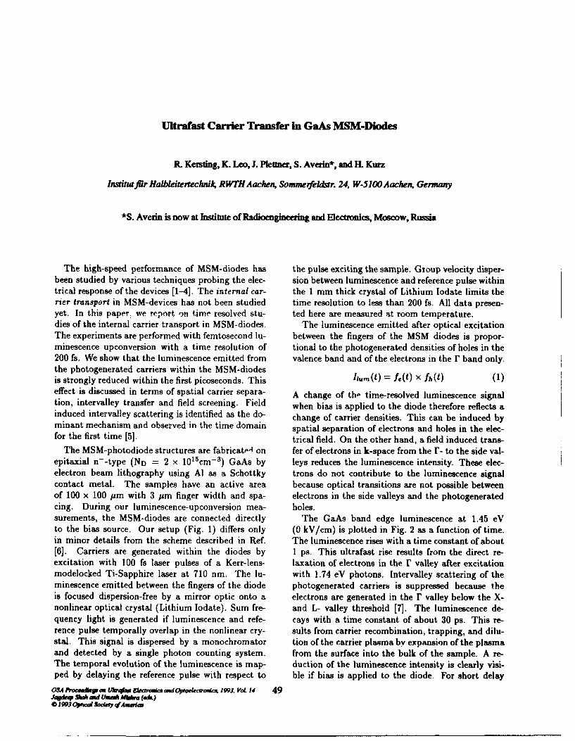
Ultrafast Carrier Transfer in GaAs MSM-Diodes
R. Kersting, K. Leo, J. Pletner, S. Averin*, and IL Kurz
Institnufjr Halbleitenechnik RWTHAachen, Sommerfeldstr. 24, W-51OOAachen, Germany
*S. Averin is now at Institute of Radioengineering and Electronics, Moscow, Russia
The high-speed performance of MSM-diodes has the pulse exciting the sample. Group velocity disper-been studied by various techniques probing the elec- sion between luminescence and reference pulse withintrical response of the devices [1-4]. The internal car- the 1 mm thick crystal of Lithium Iodate limits therier transport in MSM-devices has not been studied time resolution to less than 200 fs. All data presen-yet. In this paper, we report on time resolved stu- ted here are measured at room temperature.dies of the internal carrier transport in MSM-diodes. The luminescence emitted after optical excitationThe experiments are performed with femtosecond lu- between the fingers of the MSM diodes is propor-minescence upconversion with a time resolution of tional to the photogenerated densities of holes in the200 fs. We show that the luminescence emitted from valence band and of the electrons in the r band only.the photogenerated carriers within the MSM-diodesis strongly reduced within the first picoseconds. This itumQ) = Me(t) X fh(t) (1)effect is discussed in terms of spatial carrier separa- A change of the time-resolved luminescence signaltion, intervalley transfer and field screening. Field when bias is applied to the diode therefore reflects ainduced intervalley scattering is identified as the do- change of carrier densities. This can be induced byminant mechanism and observed in the time domain spatial separation of electrons and holes in the elec-for the first time [5]. trical field. On the other hand, a field induced trans-
The MSM-photodiode structures are fabricat-1 on fer of electrons in k-space from the r- to the side val-epitaxial n--type (ND = 2 x 101 5 cm- 3) GaAs by leys reduces the luminescence intensity. These elec-electron beam lithography using Al as a Schottky trons do not contribute to the luminescence signalcontact metal. The samples have an active area because optical transitions are not possible betweenof 100 x 100 pm with 3 pm finger width and spa- electrons in the side valleys and the photogeneratedcing. During our luminescence-upconversion mea- holes.surements, the MSM-diodes are connected directly The GaAs band edge luminescence at 1.45 eVto the bias source. Our setup (Fig. 1) differs only (0 kV/cm) is plotted in Fig. 2 as a function of time.in minor details from the scheme described in Ref. The luminescence rises with a time constant of about[6]. Carriers are generated within the diodes by 1 ps. This ultrafast rise results from the direct re-excitation with 100 fs laser pulses of a Kerr-lens- laxation of electrons in the r valley after excitationmodelocked Ti-Sapphire laser at 710 nm. The lu- with 1.74 eV photons. Intervalley scattering of theminescence emitted between the fingers of the diode photogenerated carriers is suppressed because theis focused dispersion-free by a mirror optic onto a electrons are generated in the r valley below the X-nonlinear optical crystal (Lithium Iodate). Sum fre- and L- valley threshold [7]. The luminescence de-quency light is generated if luminescence and refe- cays with a time constant of about 30 ps. This re-rence pulse temporally overlap in the nonlinear cry- suits from carrier recombination, trapping, and dilu-stal. This signal is dispersed by a monochromator tion of the carrier plasma by expansion of the plasmaand detected by a single photon counting system. from the surface into the bulk of the sample. A re-The temporal evolution of the luminescence is map- duction of the luminescence intensity is clearly visi-ped by delaying the reference pulse with respect to ble if bias is applied to the diode. For short delay
oSA Avocj~k on Mr mk wikandOoprevW•c 1993. VoL 14 49Jqdeq MA ad WIM* kbbu (*A)o 1993Opft~cs Sociei) qjAnimef
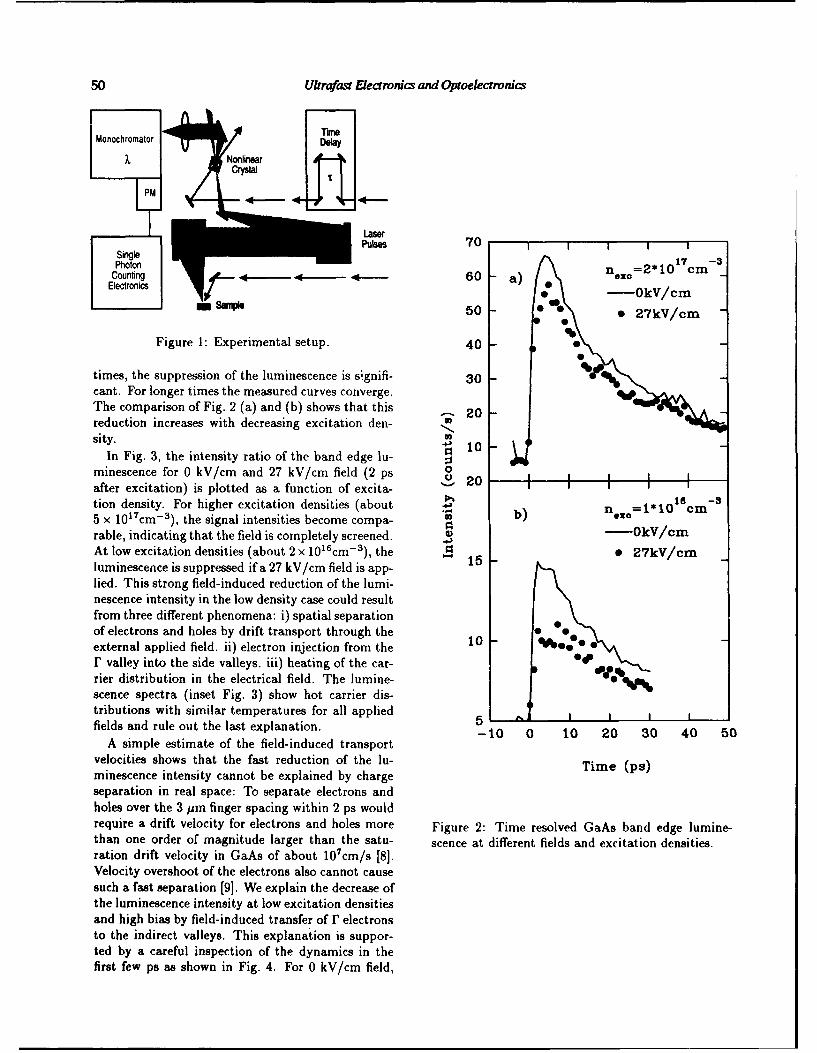
50 Ultrafasl Fiectronics and Optoeaecrronics
MonochromatorDea
NonlinearCrystal
PM
SPulses 70 1 17Single
Counting 60 a) =2*101cmElectronics - OkV/cm
M Sme 50 - 27kV/cm
Figure 1: Experimental setup. 40 -- %
times, the suppression of the luminescence is signifi- 30 °cant. For longer times the measured curves converge.The comparison of Fig. 2 (a) and (b) shows that this 220reduction increases with decreasing excitation den-sity. ~10
In Fig. 3, the intensity ratio of the band edge lu-minescence for 0 kV/cm and 27 kV/cm field (2 ps 0after excitation) is plotted as a function of excita- 20
is -3tion density. For higher excitation densities (about * bm5 x 1017 cm-3 ), the signal intensities become compa- b) Szc
rable, indicating that the field is completely screened. - OkV/cm
At low excitation densities (about 2 x 101 6 cm- 3 ), the - 15 27kV/cmluminescence is suppressed if a 27 kV/cm field is app-lied. This strong field-induced reduction of the lumi-nescence intensity in the low density case could resultfrom three different phenomena: i) spatial separationof electrons and holes by drift transport through theexternal applied field. ii) electron injection from the 10r valley into the side valleys. iii) heating of the car-rier distribution in the electrical field. The lumine- leescence spectra (inset Fig. 3) show hot carrier dis-tributions with similar temperatures for all applied 5fields and rule out the last explanation. -10 0 10 20 30 40 50
A simple estimate of the field-induced transportvelocities shows that the fast reduction of the lu- Time (ps)minescence intensity cannot be explained by chargeseparation in real space: To separate electrons andholes over the 3 pm finger spacing within 2 ps wouldrequire a drift velocity for electrons and holes more Figure 2: Time resolved GaAs band edge lumine-than one order of magnitude larger than the satu- scence at different fields and excitation densities.ration drift velocity in GaAs of about 1O7cm/s [8].Velocity overshoot of the electrons also cannot causesuch a fast separation [9]. We explain the decrease ofthe luminescence intensity at low excitation densitiesand high bias by field-induced transfer of r electronsto the indirect valleys. This explanation is suppor-ted by a careful inspection of the dynamics in thefirst few ps as shown in Fig. 4. For 0 kV/cm field,
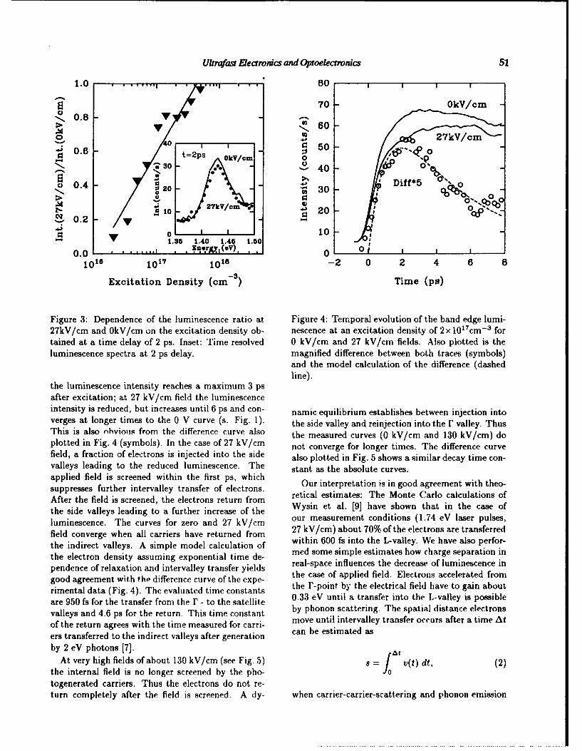
Ultr/ast Eleanroncs and Optoelectronics 51
1.0 80
j70 -OVc0O.8 V -
V N 60
• - 0.6 40 I50-t=2ps •OkV/cm 0
N. ~30
f**
~0 v5o/'- 0 •>.0. /=p ::o 0 °. 7kV/cm
q 200o -0
0.4.)Dff5
-1.33 1.40 1.46 1.6
0.0.... ......... n.er~gl(.V), 0____________________
10l6 i017 1018 -2 0 2 4 6 8
Excitation Density (cm- ) Time (ps)
Figure 3: Dependence of the luminescence ratio at Figure 4: Temporal evolution of the band edge lumi-27k V/cm and 0kV/cm on the excitation density ob- nescence at an excitation density of 2x 10 1 7cm-s fortained at a time delay of 2 ps. Inset: Time resolved 0 kV/cm and 27 kV/cm fields. Also plotted is theluminescence spectra at 2 ps delay. magnified difference between both traces (symbols)
and the model calculation of the difference (dashedline).
the luminescence intensity reaches a maximum 3 psafter excitation; at 27 kV/cm field the luminescence
intensity is reduced, but increases until 6 ps and con- namic equilibrium establishes between injection intoverges at longer times to the 0 V curve (s. Fig. 1). the side valley and reinjection into the F valley. ThusThis is also obhvioiis from the difference curve also the measured curves (0 kV/cm and 130 kV/cm) doplotted in Fig. 4 (symbols). In the case of 27 kV/cm not converge for longer times. The difference curvefield, a fraction of electrons is injected into the side also plotted in Fig. 5 shows a similar decay time con-valleys leading to the reduced luminescence. The stant as the absolute curves.applied field is screened within the first ps, which Oritrrtto si odareetwt hosuppresses further intervalley transfer of electrons.After the field is screened, the electrons return from retical estimates: The Monte Carlo calculations ofthe side valleys leading to a further increase of the Wysin et al. [9] have shown that in the case ofluminescence. The curves for zero and 27 kV/cm our measurement conditions (1.74 eV laser pulses,field converge when all carriers have returned from 27 kV/cm) about 70% of the electrons are transferred
the ndiectvallys.A smplemodl clcultio of within 600 fs into the L-valley. We have also perfor-
the electron density assuming exponential time de- mdsm ipeetmtshwcag eaainipendence of relaxation and intervalley transfer yields real-space influences the decrease of luminescence ingood agreement wit~h the difference curve of the expe- the case of applied field. Electrons accelerated from
rimetaldata(Fi. 4) Th evluatd tme cnstnts the F-point by the electrical field have to gain aboutare 950 fs for the transfer from the F - to the satellite 0.33 eV until a transfer into the L-valley is possiblevalleys and 4.6 ps for the return. This time constant by phonon scattering. The spatial distance electronsof the return agrees with the time measured for carri- move until intervalley transfer occurs after a time Aters transferred to the indirect valleys after generation can be estimated asby 2 eV photons [7].
At very high fields of about 130 kV/cm (see Fig. 5) s= / v(t) dt, (2)the internal field is no longer screened by the pho- Otogenerated carriers. Thus the electrons do not re-turn completely after the field is screened. A dy- when carrier-carrier-scattering and phonon emission
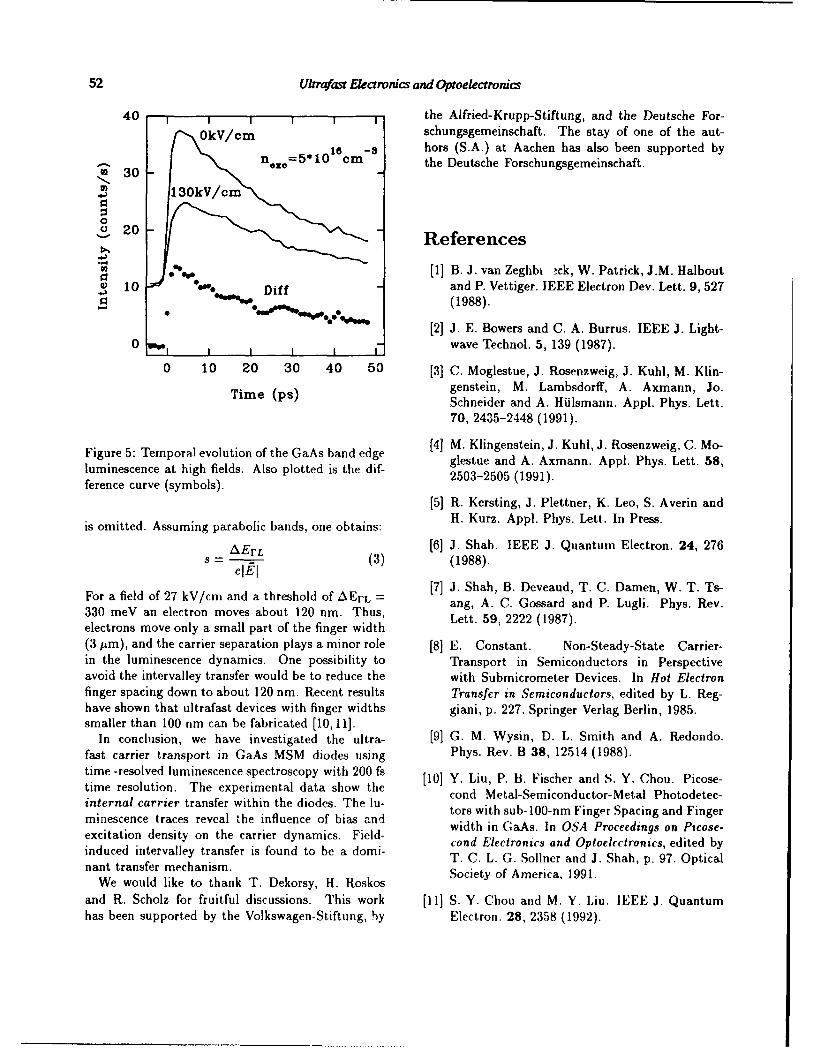
52 Uftrafast Electronics and Optoelecrronics
40 1 1 1 1 the Alfried-Krupp-Stiftung, and the Deutsche For-OkV/cm schungsgemeinschaft. The stay of one of the aut-
n n =510 1 6cm - hors (S.A.) at Aachen has also been supported by
" 30Sz the Deutsche Forschungsgemeinschaft.
30
,a 20 References
[1] B. J. van Zeghbi ýck, W. Patrick, J.M. Halbout
"10 Diff and P. Vettiger. IEEE Electron Dev. Lett. 9, 5270%%0(1988).
[2] J. E. Bowers and C. A. Burrus. IEEE J. Light-
0 wave Technol. 5, 139 (1987).
0 10 20 30 40 50 [3] C. Moglestue, J. Rosenzweig, J. Kuhl, M. Klin-
genstein, M. Lambsdorff, A. Axmann, Jo.Time (ps) Schneider and A. Hiilsmann. Appl. Phys. Lett.
70, 2435-2448 (1991).
Figure 5: Temporal evolution of the GaAs band edge [4] M. Klingenstein, J. Kuhl, J. Rosenzweig, C. Mo-
luminescence at high fields. Also plotted is the dif- glestue and A. Axmann. Appl. Phys. Lett. 58,
ference curve (symbols). 2503-2505 (1991).
[5] R. Kersting, J. Plettner, K. Leo, S. Averin and
is omitted. Assuming parabolic bands, one obtains: H. Kurz. Appl. Phys. Lett. In Press.
AErL [6] J. Shah. IEEE J. Quantum Electron. 24, 276s =- lf (3) (1988).
[7] J. Shah, B. Deveaud, T. C. Damen, W. T. Ts-For a field of 27 kV/cm and a threshold of AErL =ang, A. C. Gossard and P. Lugli. Phys. Rev.330 meV an electron moves about 120 nm. Thus, Lett. 59, 2222 (1987).electrons move only a small part of the finger width(3 Mm), and the carrier separation plays a minor role [8] E. Constant. Non-Steady-State Carrier-in the luminescence dynamics. One possibility to Transport in Semiconductors in Perspectiveavoid the intervalley transfer would be to reduce the with Submicrometer Devices. In Hot Electronfinger spacing down to about 120 nm. Recent results Transfer in Semiconductors, edited by L. Reg-have shown that ultrafast devices with finger widths giani, p. 227. Springer Verlag Berlin, 1985.smaller than 100 nm can be fabricated [10, 11].
In conclusion, we have investigated the ultra- [9] G. M. Wysin, D. L. Smith and A. Redondo.fast carrier transport in GaAs MSM diodes using Phys. Rev. B 38, 12514 (1988).
time -resolved luminescence spectroscopy with 200 fs [10] Y. Liu, P. B. Fischer and S. Y. Chou. Picose-time resolution. The experimental data show the cond Metal-Semiconductor-Metal Photodetec-internal carrier transfer within the diodes. The lu- cond Metal-Semindcr-Meal hodettors with sub-100-nm Finger Spacing and Fingerminescence traces reveal the influence of bias and width in GaAs. In OSA Proceedings on Picose-excitation density on the carrier dynamics. Field- cond Electronics and Oploelccronics, edited byinduced intervalley transfer is found to be a domi- T. C. L. G. Sollner and J. Shah, p. 97. Opticalnant transfer mechanism.
We would like to thank T. Dekorsy, H. Roskos Society of America, 1991.and R. Scholz for fruitful discussions. This work [11] S. Y. Chou and M. Y. Liu. IEEE J. Quantumhas been supported by the Volkswagen-Stiftung, by Electron. 28, 2358 (1992).
Ultrafast Metal-Semiconductor-Metal Photodetectorswith Nanometer Scale Finger Spacing and Width
Mark Y. Liu and Stephen Y. Chou
Department of Electrical Engineering, University of Minnesota, Minneapolis, Minnesota 55455
Sotiris Alexandrou and Thomas Y. Hsiang
Laboratory for Laser Energetics, University of Rochester, Rochester, New York 14623
Abstract coplanar striplines were fabricated on the substrates
and integrated with the detectors. Both shunt and in-We report the fabrication and measurement of ultrafast line connection of detectors and transmission linesnanoscale metal-semiconductor-metal photodetectors. were used in the measurements. Nanometer scaleThe finger spacing and width as small as 25 nm are fingers were fabricated using electron beam litho-fabricated using electron beam lithography. Electro- graphy and a lift-off technique. Finger spacing andoptic sampling was performed at various wavelengths width as small as 25 nm have been achieved (Fig. 1).to measure the detectors' response time. The fastest To understand the operation of the nanoscaledetectors have response times and 3-dB bandwidths of MSMPDs, we used a one-dimensional Monte-Carlo0.87 ps and 510 GHz on low-temperature GaAs, 1.5 ps method to simulate the intrinsic carrier transit timeand 300 GHz on bulk GaAs, and 3.7 ps and 110 GHz between the metal fingers, and calculated deviceon bulk Si. To our knowledge, they are the fastest capacitance [8]. Based on the theoretical and experi-photodetectors of their kind. Scaling rules are also mental data, we propose the scaling rules for high-proposed. speed and high-sensitivity MSMPD's. (1) Reduce
finger spacing to decrease carrier transit time,therefore increase speed for transit-time-limited
Much progress has been reported recently on MSMPD's and increase sensitivity for recombination-ultrafast metal-semiconductor-metal photodetectors time-limited MSMPD's. (2) Reduce finger width and(MSMPD's). MSMPD's on many semiconductor detector area to decrease the detector capacitance. (3)materials, such as GaAs [1-31, Si [4,5], InGaAs [6,7], Reduce light absorption depth to eliminate carriershave demonstrated picosecond response time. Proper generated deep inside the semiconductor bulk. (4) Usescaling of the detector finger spacing and finger width shorter and thicker metal fingers to reduce the fingeris essential to achieve high speed and high sensitivity lesistance.[8]. In this paper, we report our work on ultrafast Electrooptic sampling measurements wereMSMPD's with nanometer scale finger structures. pt:rformed to measure the impulse responses of theHigh-speed characterization was performed using an MSMPD's. A colliding-pulse modelocked dye laserelectrooptic sampling system consisting of a with 100 fs pulsewidth and 620 nm wavelength waswavelength tunable femtosecond Ti:A12 0 3 laser. used for measuring the GaAs detectors 191. As shownMeasurements show that the dctectors are the fastest of in Fig. 2, the MSMPD on LT-GaAs with 300 nmtheir kind. Impulse response of Si MSMPD's strongly finger spacing and width has a response time of 0.87depends on the laser wavelength, which indicates that ps and 3-dB bandwidth of 510 GHz, which are limitedthe carriers generated deep i',,ide the semiconductor by the carrier recombination time. However, as thebulk play an important role in detector operation. finger spacing and width decrease, the device
Our MSMPD's are fabricated on three different capacitance increases since the device active areasemiconductor materials: LT-GaAs, bulk GaAs, and keeps unchanged [81, and the response time is limitedbulk Si. For electrooptic sampling measurement, by the RC time constant (Table 1).
OSA Procvedgngs on Ulrafnst Electronics and Optoelearownicx 1993, VoL 14 53Jagdeep Shah and Unesh Mishra (eds )0 1993 Oyfkal Society ofAmerica
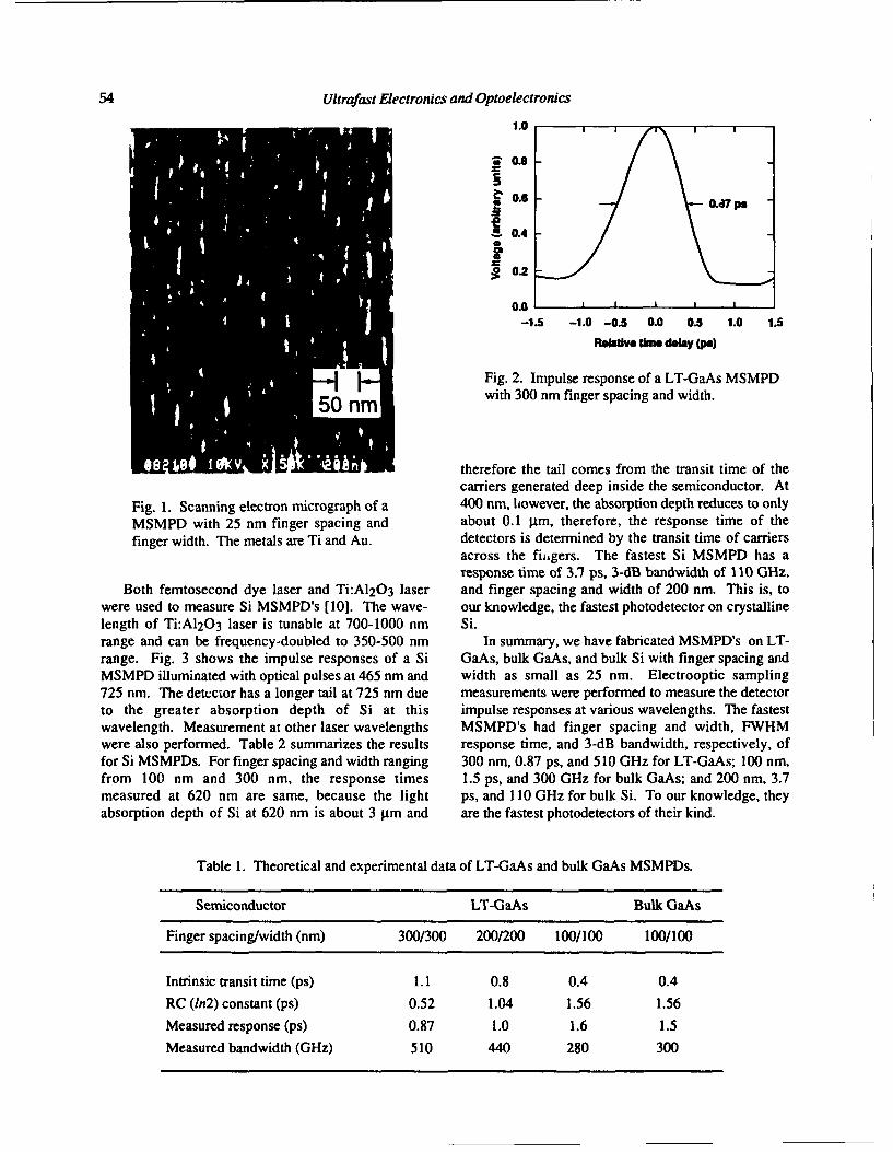
54 Ultrafast Electronics and Optoelectronics
1.0
V 0.8
0.6
,S 0.4
020 .2
0.0 Ii I
-1.5 -1.0 -0.5 0.0 0.5 1.0 1.5
Relative ime delay (pa)
Fig. 2. Impulse response of a LT-GaAs MSMPDwith 300 nm finger spacing and width.
m therefore the tail comes from the transit time of thecarriers generated deep inside the semiconductor. At
Fig. 1. Scanning electron micrograph of a 400 nm, however, the absorption depth reduces to onlyMSMPD with 25 nm finger spacing and about 0.1 gtm, therefore, the response time of thefinger width. The metals are Ti and Au. detectors is determined by the transit time of carriers
across the fiigers. The fastest Si MSMPD has aresponse time of 3.7 ps, 3-dB bandwidth of 110 GHz,
Both femtosecond dye laser and Ti:A12 03 laser and finger spacing and width of 200 nm. This is, towere used to measure Si MSMPD's [10]. The wave- our knowledge, the fastest photodetector on crystallinelength of Ti:A12 0 3 laser is tunable at 700-1000 nm Si.range and can be frequency-doubled to 350-500 nm In summary, we have fabricated MSMPD's on LT-range. Fig. 3 shows the impulse responses of a Si GaAs, bulk GaAs, and bulk Si with finger spacing andMSMPD illuminated with optical pulses at 465 nm and width as small as 25 nm. Electrooptic sampling725 nm. The detector has a longer tail at 725 nm due measurements were performed to measure the detectorto the greater absorption depth of Si at this impulse responses at various wavelengths. The fastestwavelength. Measurement at other laser wavelengths MSMPD's had finger spacing and width, FWHMwere also performed. Table 2 summarizes the results response time, and 3-dB bandwidth, respectively, offor Si MSMPDs. For finger spacing and width ranging 300 nm, 0.87 ps, and 510 GHz for LT-GaAs; 100 nm,from 100 nm and 300 nm, the response times 1.5 ps, and 300 GHz for bulk GaAs; and 200 nm, 3.7measured at 620 nm are same, because the light ps, and 110 GHz for bulk Si. To our knowledge, theyabsorption depth of Si at 620 nm is about 3 gtm and are the fastest photodetectors of their kind.
Table 1. Theoretical and experimental data of LT-GaAs and bulk GaAs MSMPDs.
Semiconductor LT-GaAs Bulk GaAs
Finger spacing/width (nm) 300/300 200/200 100/100 100/100
Intrinsic transit time (ps) 1.1 0.8 0.4 0.4
RC (Wn2) constant (ps) 0.52 1.04 1.56 1.56
Measured response (ps) 0.87 1.0 1.6 1.5
Measured bandwidth (GHz) 510 440 280 300
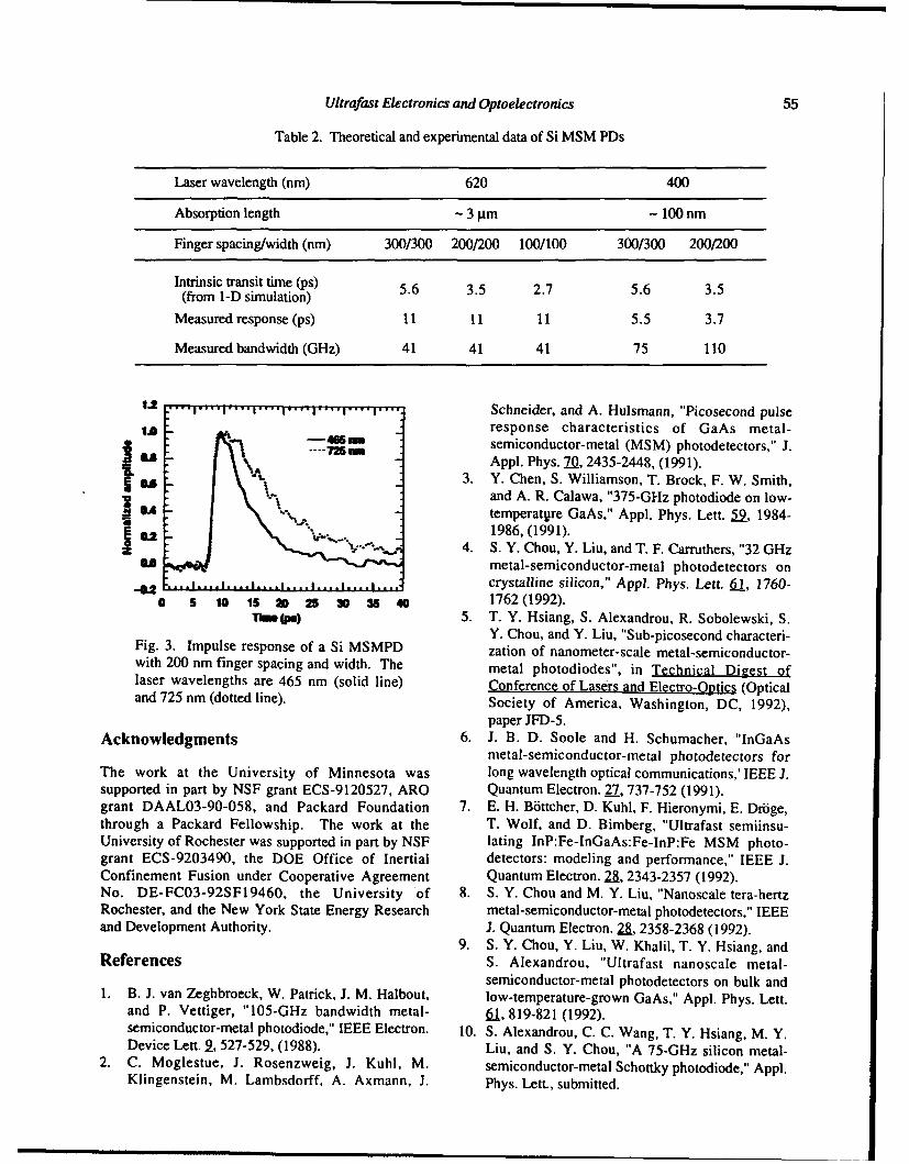
Ultrafast Electronics and Optoelectronics 55
Table 2. Theoretical and experimental data of Si MSM PDs
Laser wavelength (nm) 620 400
Absorption length - 3 g.m - 100 nm
Finger spacing/width (nm) 300/300 200/200 100/100 300/300 200/200
Intrinsic transit time (ps) 5.6 3.5 2.7 5.6 3.5(from 1-D simulation)
Measured response (ps) 11 11 11 5.5 3.7
Measured bandwidth (GHz) 41 41 41 75 110
1. . I Schneider, and A. Hulsmann, "Picosecond pulseresponse characteristics of GaAs metal-' .4 osemiconductor-metal (MSM) photodetectors," J.
---- 75 . ma Appl. Phys. IQ, 2435-2448, (1991).
5.3. Y. Chen, S. Williamson, T. Brock, F. W. Smith,'2 kand A. R. Calawa, "375-GHz photodiode on low-a 04A temperatgre GaAs," Appl. Phys. Lett. 5U, 1984-
6 ".1986, (1991).0 -_.1 -".. 4. S. Y. Chou, Y. Liu, and T. F. Carruthers, "32 GHzLU metal-semiconductor-metal photodetectors on
...2 crystalline silicon," Appl. Phys. Lett. 6_1, 1760-0 5 10 15 2 2 3 35 0 1762 (1992).
"TiMo(Ps) 5. T. Y. Hsiang, S. Alexandrou, R. Sobolewski, S.Y. Chou, and Y. Liu, "Sub-picosecond characteri-Fig. 3. Impulse response of a Si MSMPD zation of nanometer-scale metal-semiconductor-
with 200 nm finger spacing and width. The metal photodiodes", in Technical Digest oflaser wavelengths are 465 nm (solid line) Conference of Lasers and Electro-Optics (Opticaland 725 nm (dotted line). Society of America, Washington, DC, 1992),
paper JFD-5.Acknowledgments 6. J. B. D. Soole and H. Schumacher, "InGaAs
metal-semiconductor-metal photodetectors forThe work at the University of Minnesota was long wavelength optical communications,' IEEE J.supported in part by NSF grant ECS-9120527, ARO Quantum Electron. 27, 737-752 (1991).grant DAAL03-90-058, and Packard Foundation 7. E. H. Bottcher, D. Kuhl, F. Hieronymi, E. Droge,through a Packard Fellowship. The work at the T. Wolf, and D. Bimberg, "Ultrafast semiinsu-University of Rochester was supported in part by NSF lating InP:Fe-InGaAs:Fe-InP:Fe MSM photo-grant ECS-9203490, the DOE Office of Inertial detectors: modeling and performance," IEEE J.Confinement Fusion under Cooperative Agreement Quantum Electron. 2&, 2343-2357 (1992).No. DE-FC03-92SF19460, the University of 8. S. Y. Chou and M. Y. Liu, "Nanoscale tera-hertzRochester, and the New York State Energy Research metal-semiconductor-metal photodetectors," IEEEand Development Authority. J. Quantum Electron. 2&, 2358-2368 (1992).
9. S. Y. Chou, Y. Liu, W. Khalil, T. Y. Hsiang, andReferences S. Alexandrou, "Ultrafast nanoscale metal-
semiconductor-metal photodetectors on bulk and1. B. J. van Zeghbroeck, W. Patrick, J. M. Halbout, low-temperature-grown GaAs," Appl. Phys. Lett.
and P. Vettiger, "105-GHz bandwidth metal- 61, 819-821 (1992).semiconductor-metal photodiode," IEEE Electron. 10. S. Alexandrou, C. C. Wang, T. Y. Hsiang, M. Y.Device Lett. 2, 527-529, (1988). Liu, and S. Y. Chou, "A 75-GHz silicon metal-
2. C. Moglestue, J. Rosenzweig, J. Kuhl, M. semiconductor-metal Schottky photodiode," Appi.Klingenstein, M. Lambsdorff, A. Axmann, J. Phys. Lett., submitted.
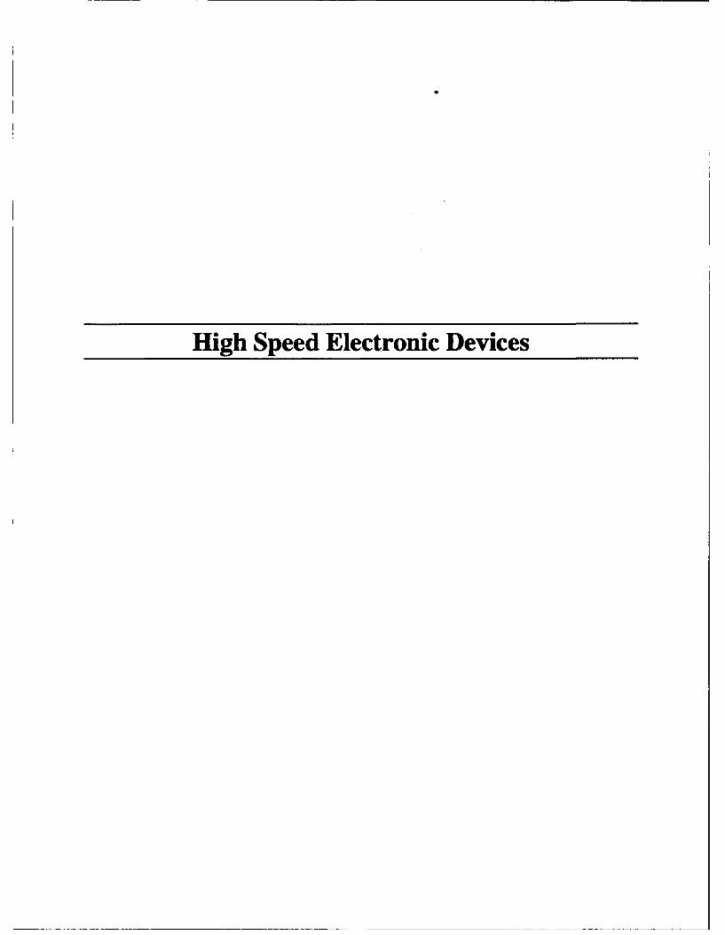
High Speed Electronic Devices
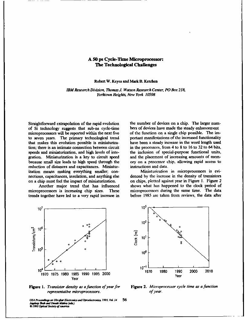
A 50 ps Cycle-Time Microprocessor:The Technological Challenges
Robert W. Keyes and Mark B. Ketchen
IBM Research Division Thomas J. Watson Research Center, PO Box 218,Yorktown Heights, New York 10598
Straightforward extrapolation of the rapid evolution the number of devices on a chip. The larger num-of Si technology suggests that sub-ns cycle-time bers of devices have made the steady enhancementmicroprocessors will be reported within the next five of the function on a single chip possible. The im-to seven years. The primary technological trend portant manifestations of the increased functionalitythat makes this evolution possible is miniaturiza- have been a steady increase in the word length usedtion; there is an intimate connection between circuit in the processors, from 4 to 8 to 16 to 32 to 64 bits,speeds and miniaturization, and high levels of inte- the inclusion of special-purpose functional units,gration. Miniaturization is a key to circuit speed and the placement of increasing amounts of mem-because small size leads to high speed through the ory on a processor chip, allowing rapid access toreduction of distances and capacitances. Miniatur- instructions and data.ization means making everything smaller; con- Miniaturization in microprocessors is evi-nections, capacitances, insulation, and anything else denced by the increase in the density of transistorson a chip must feel the impact of miniaturization, on chips, plotted against year in Figure 1. Figure 2
Another major trend that has influenced shows what has happened to the clock period ofmicroprocessors is increasing chip sizes. These microprocessors during the same time. The datatrends together have led to a very rapid increase in before 1985 are taken from reviews, the data after
0
0
0 00 102 0 0
V4 0 0
E 101- 0
-01o• - 000 0
C, 0 80
0 go10
0- 00"io 01I I
104- 1- 1 9 70 19 180 19 190 20 100 20101970 1975 1980 1985 1990 1995 2000 Year
Year
Figure 1. Transistor density as a function of year for Figure 2. Microprocessor cycle time as a functionrepresentative microprocessors. of year.
OSA Proceedhw on UlkraN Efr and Op iatou'cm 1993, VoL 14 56Jq#dp • tid Uw Ma*"w (•)
S1993 •pcal Sodey qfmerlca
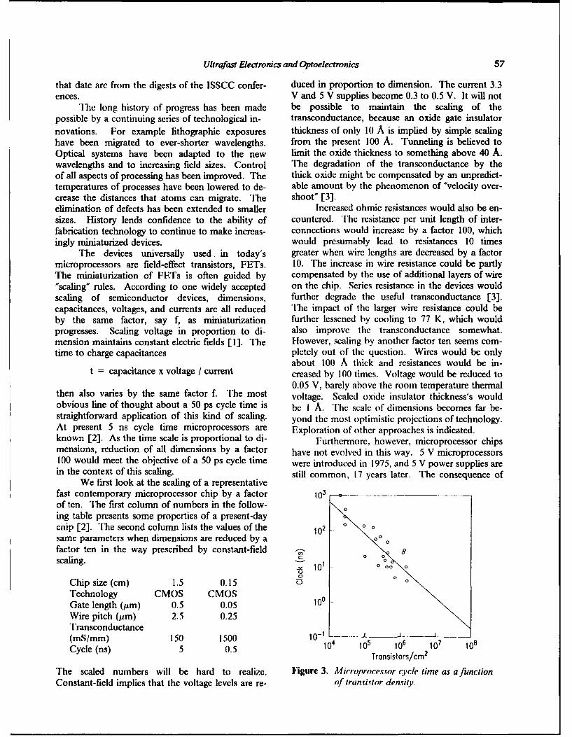
Ultrafast Electronics and Optoelectronics 57
that date are from the digests of the ISSCC confer- duced in proportion to dimension. The current 3.3ences. V and 5 V supplies become 0.3 to 0.5 V. It will not
The long history of progress has been made be possible to maintain the scaling of thepossible by a continuing series of technological in- transconductance, because an oxide gate insulator
novations. For example lithographic exposures thickness of only 10 A is implied by simple scalinghave been migrated to ever-shorter wavelengths, from the present 100 A. Tunneling is believed toOptical systems have been adapted to the new limit the oxide thickness to something above 40 A.wavelengths and to increasing field sizes. Control The degradation of the transconductance by theof all aspects of processing has been improved. The thick oxide might be compensated by an unpredict-temperatures of processes have been lowered to de- able amount by the phenomenon of 'velocity over-crease the distances that atoms can migrate. The shoot" [3].elimination of defects has been extended to smaller Increased ohmic resistances would also be en-sizes. History lends confidence to the ability of countered. The resistance per unit length of inter-fabrication technology to continue to make increas- connections would increase by a factor 100, whichingly miniaturized devices, would presumably lead to resistances 10 times
The devices universally used in today's greater when wire lengths are decreased by a factormicroprocessors are field-effect transistors, FETs. 10. The increase in wire resistance could be partlyThe miniaturization of FETs is often guided by compensated by the use of additional layers of wire"scaling" rules. According to one widely accepted on the chip. Series resistance in the devices wouldscaling of semiconductor devices, dimensions, further degrade the useful transconductance [3].capacitances, voltages, and currents are all reduced The impact of the larger wire resistance could beby the same factor, say f, as miniaturization further lessened by cooling to 77 K, which wouldprogresses. Scaling voltage in proportion to di- also improve the transconductance somewhat.mension maintains constant electric fields [1]. The Hlowever, scaling by another factor ten seems com-time to charge capacitances pletely out of the question. Wires would be only
about 100 A thick and resistances would be in-t = capacitance x voltage / current creased by 100 times. Voltage would be reduced to
0.05 V, barely above the room temperature thermalthen also varies by the same factor f. The most voltage. Scaled oxide insulator thickness's wouldobvious line of thought about a 50 ps cycle time is be I A. The scale of dimensions becomes far be-straightforward application of this kind of scaling. yond the most optimistic projections of technology.At present 5 ns cycle time microprocessors are Exploration of other approaches is indicated.known [2]. As the time scale is proportional to di- Furthermore, however, microprocessor chipsmensions, reduction of all dimensions by a factor have not evolved in this way. 5 V microprocessors100 would meet the objective of a 50 ps cycle time were introduced in 1975, and 5 V power supplies arein the context of this scaling, still common, 17 years later. The consequence of
We first look at the scaling of a representativefast contemporary microprocessor chip by a factor 10&r-of ten. The first column of numbers in the follow- 0ing table presents some properties of a present-daycnip [2]. The second column lists the values of the 102 0 0
same parameters when dimensions are reduced by a 00 0factor ten in the way prescribed by constant-field 00
scaling. 00 0
-• 101 0o 0
Chip size (cm) 1.5 0.15 0
Technology CMOS CMOSGate length (jim) 0.5 0.05 10°Wire pitch (ttm) 2.5 0.25Transconductance(mS/mm) 150 1500 10-1 1
Cycle (ns) 5 0.5 o4 105 106 210 101Transistors/cm2
The scaled numbers will be hard to realize. Figure 3. Microprocessor cycle time as a functionConstant-field implies that the voltage levels are re- of transistor density.
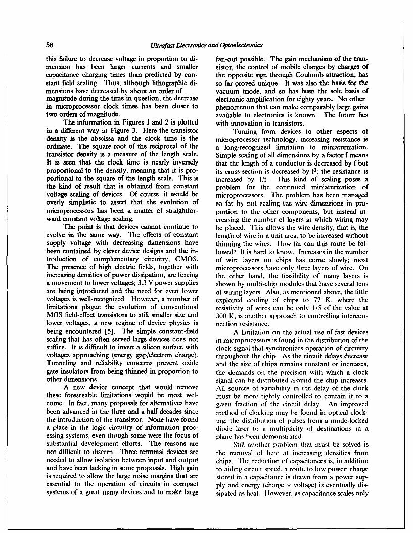
58 Ultrafast Electronics and Optoelectronics
this failure to decrease voltage in proportion to di- fan-out possible. The gain mechanism of the tran-mension has been larger currents and smaller sistor, the control of mobile charges by charges ofcapacitance charging times than predicted by con- the opposite sign through Coulomb attraction, hasstant field scaling. Thus, although lithographic di- so far proved unique. It was also the basis for themensions have decreased by about an order of vacuum triode, and so has been the sole basis ofmagnitude during the time in question, the decrease electronic amplification for eighty years. No otherin microprocessor clock times has been closer to phenomenon that can make comparably large gainstwo orders of magnitude. available to electronics is known. The future lies
The information in Figures 1 and 2 is plotted with innovation in transistors.in a different way in Figure 3. Here the transistor Turning from devices to other aspects ofdensity is the abscissa and the clock time is the microprocessor technology, increasing resistance isordinate. The square root of the reciprocal of the a long-recognized limitation to miniaturization.transistor density is a measure of the length scale. Simple scaling of all dimensions by a factor f meansIt is seen that the clock time is nearly inversely that the length of a conductor is decreased by f butproportional to the density, meaning that it is pro- its cross-section is decreased by P2; the resistance isportional to the square of the length scale. This is increased by I/f. This kind of scaling poses athe kind of result that is obtained from constant problem for the continued miniaturization ofvoltage scaling of devices. Of course, it would be microprocessors. The problem has been managedoverly simplistic to assert that the evolution of so far by not scaling the wire dimensions in pro-microprocessors has been a matter of straightfor- portion to the other components, but instead in-ward constant voltage scaling, creasing the number of layers in which wiring may
The point is that devices cannot continue to be placed. This allows the wire density, that is, theevolve in the same way. The effects of constant length of wire in a unit area, to be increased withoutsupply voltage with decreasing dimensions have thinning the wires. I low far can this route be fol-been contained by clever device designs and the in- lowed? It is hard to know. Increases in the numbertroduction of complementary circuitry, CMOS. of wire layers on chips has come slowly; mostThe presence of high electric fields, together with microprocessors have only three layers of wire. Onincreasing densities of power dissipation, are forcing the other hand, the feasibility of many layers isa movement to lower voltages; 3.3 V power supplies shown by multi-chip modules that have several tensare being introduced and the need for even lower of wiring layers. Also, as mentioned above, the littlevoltages is well-recognized. However, a number of exploited cooling of chips to 77 K, where thelimitations plague the evolution of conventional resistivity of wires can be only 1/5 of the value atMOS field-effect transistors to still smaller size and 300 K, is another approach to controlling intercon-lower voltages, a new regime of device physics is nection resistance.being encountered [5]. The simple constant-field A limitation on the actual use of fast devicesscaling that has often served large devices does not in microprocessors is found in the distribution of thesuffice. It is difficult to invert a silicon surface with clock signal that synchronizes operation of circuitryvoltages approaching (energy gap/electron charge). throughout the chip. As the circuit delays decreaseTunneling and reliability concerns prevent oxide and the size of chips remains constant or increases,gate insulators from being thinned in proportion to the demands on the precision with which a clockother dimensions. signal can be distributed around the chip increases.
A new device concept that would remove All sources of variability in the delay of the clockthese foreseeable limitations would be most wel- must be more tightly controlled to contain it to acome. In fact, many proposals for alternatives have given fraction of the circuit delay. An improvedbeen advanced in the three and a half decades since method of clocking may be found in optical clock-the introduction of the transistor. None have found ing; the distribution of pulses from a mode-lockeda place in the logic circuitry of information proc- diode laser to a multiplicity of destinations in aessing systems, even though some were the focus of plane has been demonstrated.substantial development efforts. The reasons are Still another problem that must be solved isnot difficult to discern. Three terminal devices are the removal of heat at increasing densities fromneeded to allow isolation between input and output chips. The reduction of capacitances is, in additionand have been lacking in some proposals. High gain to aiding circuit speed, a route to low power; chargeis required to allow the large noise margins that are stored in a capacitance is drawn from a power sup-essential to the operation of circuits in compact ply and energy (charge x voltage) is eventually dis-systems of a great many devices and to make large sipated as heat. I lowever, as capacitance scales only
Ultrafast Electronics and Optoelectronics 59
linearly with dimension and the number of compo- Instead of attempting to discuss other difficultnents per unit area increases quadratically as size is system issues, a recently proposed rough guide todecreased, the density at which electrical energy is system performance may be used to estimate theconverted to heat increases. The density of heat kind of chip that might be built from our speculativeproduction is further increased by the faster opera- technology [7]. The estimate of cycle time sug-tion possible with smaller components. gested by I Isi and Tucker may be stated in the form
Fortunately, several approaches can be com-bined to control dissipation. The use of dynamic 'C = tL + fiA 112ItD.circuitry, which uses energy only when a switching Here tL is the logic delay time, t
D is the delay peroccurs, has been introduced over the last decade. unit length on the wiring, and A is the system area.Controlling power is an additional motivation for By fitting the parameters a and #1 to the perform-the reduction of voltages, as mentioned in con- ance of large systems and making a bold leap tonection with devices. The use of "sleep modes," microprocessors with t = 2 ps and t, = 70 ps/cmturning off parts of a chip that are not in active use m icdo thateas 50s psi cycle, time is a n e wt a
we find that a 50 ps cycle time is attained with auntil they are needed, is becoming common. Nev- chip of area 0.02 cm 2. While this is a small chip inertheless, cooling of high performance micro- the perspective of contemporary microprocessors itprocessor chips will continue to demand attention. contains four million transistors in the assumed
Comparison with current microprocessor technology.technologies and extrapolation suggests that a 50 Thus innovation in many areas of technology,rn technology would satisfy the interconnection wiring, lithography, circuit and device concepts,
requirements for a chip that contained 2x 10⁸ tran- power management and cooling, and clocking willsistors per cm2 with a cycle time of 50 ps. Inter- be needed to sustain the momentum of the advanc-connections would be 150 nm metal lines and ing microprocessor art. There are also many op-spaces in four layers. A typical wire, 15 transistor portunities, in the form of heterojunctions andpitches or 10 fim long, would have a resistance of variable band gaps, new dielectrics, and new proc-10 ohms and a capacitance of I IF. The wire RC essing methods to be exploited. The 50 ps cycleproduct is only 10 fs, compared to the approxi- time processor appears to be not far beyond themately 1 or 2 ps risetime required of the circuit and reach of technologies that are in view at this time.the 0.1 ps propagation time on the wire. A 1 mAcurrent in a wire would mean a current density of5x10 6 A/cm 2, high, but probably not beyond the RFFFREt-NCESrange to be expected of new alloys and structures inthe next decade. The demands on lithography are 1. R. I1. l)ennard, et al, IEEE J. Sol.-State Ckts.roughly comparable to those anticipated for 1 9, 256-68 (1974).gigabit memory chips.
Advances in device properties that cannot 2. IEEE International Solid-State Circuits Confer-now be foreseen will be needed. Containment of ence Digest, Session 6, 104-115 (1992).heat production will allow a power supply voltageno larger than I V. Even allowing for an improved 3. G. A. Sai-llalasz, ct al, IEEE Electron Devicedielectric, each logic gate would have a capacitive Lett. ED)L-9, 464 (1988); G. G. Shahidi, D. A.load of I WF. Obtaining I ps pulse rise times will Antonidas, and I1. 1. Smith IEIE Electron Deviceapparently require devices with a transconductance Lett. EDI -9, 94 (1988).of 0.002 to 0.004 S in an area no greater than 0.514m 2 , corresponding to at least 5 S/rnm in a field- 4. M. Nagata, IFFF. J. Sol.-St. Circuits 27, 465-72effect transistor. The characteristics of a ý0 nmn gate (1992).length silicon MOSFET recently proposed and an-alyzed approach those of the required device within 5. 1). J. Frank, S. F. Laux, and M. V. Fischetti,a factor of two [5]. IEi)M 92, paper 21.1, 553-556 (1992).
Ileat removal technology will also be strained.The wire density allows a capacitance density of 25 6. ). 13. Tuckerman and R. F. W. Pease, IEEEnF/cm 2 to be estimated. With a 50 ns cycle the Electron Device Letters EDL-2, 126-129 (1981).capacitance may be charged perhaps every 200 ps,and with voltage of 1 V, 100 W/cm 2 will be dissi- 7. C. G. Ilsi and S. G. Tucker, 1990 IEEE Interna-pated. With considerable effort, the removal of heat tional Conference on Computer Design, 49-55at such density has been demonstrated [6]. (1990).
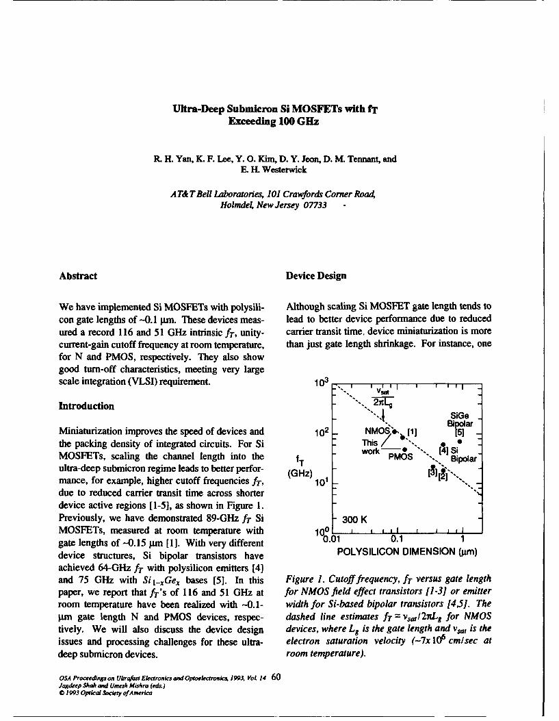
Ultra-Deep Submieron Si MOSFETs with fTrExceeding 100 GHz
RL H. Yan, K. F. Lee, Y. O. Kim, D. Y. Jeon, D. K Tennantý andE. H. Westerwick
A T& T Bell Laboratories, 101 Crawfords Corner Roa4Holmdel New Jersey 07733 .
Abstract Device Design
We have implemented Si MOSFETs with polysili- Although scaling Si MOSFET gate length tends tocon gate lengths of --0.1 jgm. These devices meas- lead to better device performance due to reducedured a record 116 and 51 GHz intrinsic fT, unity- carrier transit time, device miniaturization is morecurrent-gain cutoff frequency at room temperature, than just gate length shrinkage. For instance, onefor N and PMOS, respectively. They also showgood turn-off characteristics, meeting very largescale integration (VLSI) requirement. 103 --
"VsatIntroduction . 2 Lg
-..4. SiGeMiniaturization improves the speed of devices and 102 NMOS.. [1] Bi]lar
the packing density of integrated circuits. For Si This • "" [work [41 SiMOSFETs, scaling the channel length into the fT PMOS '-.. Bipolar
ultra-deep submicron regime leads to better perfor- (GHz)mance, for example, higher cutoff frequencies fT, 101due to reduced carrier transit time across shorterdevice active regions [1-51, as shown in Figure 1.Previously, we have demonstrated 89-GHz fT Si 300 KMOSFETs, measured at room temperature with 1 00 i , * I
gate lengths of -0.15 pm [1]. With very different 0.01 0.1 1
device structures, Si bipolar transistors have POLYSILICON DIMENSION (gm)
achieved 64-GHz fT with polysilicon emitters [4]and 75 GHz with Si i-Ge. bases [5]. In this Figure 1. Cutoff frequency, fT versus gate lengthpaper, we report that fT's of 116 and 51 GHz at for NMOS field effect transistors 11-3] or emitterroom temperature have been realized with -0.1- width for Si-based bipolar transistors [4,51. Thepim gate length N and PMOS devices, respec- dashed line estimates fT = vsaul2rLs for NMOStively. We will also discuss the device design devices, where Lg is the gate length and vsal is theissues and processing challenges for these ultra- electron saturation velocity (-7x 106 cm/sec atdeep submicron devices, room temperature).
OSA Proceedingson Uitralast Elearonics and mOptoeleronc& 1993, VoL 14 60Jagdeep Shah and Umesh Mishra (eds)0 1993 Optical Society ofAmerica
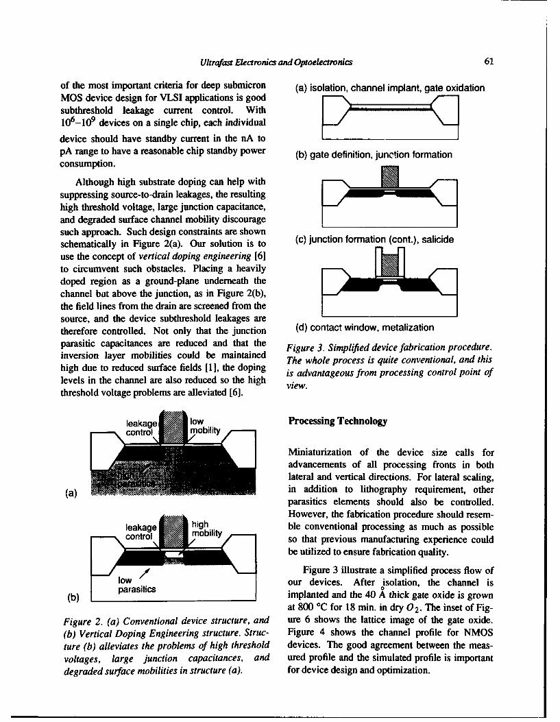
Ultrafast Elecronics and Optoelectronics 61
of the most important criteria for deep submicron (a) isolation, channel implant, gate oxidationMOS device design for VLSI applications is goodsubthreshold leakage current control. With106-109 devices on a single chip, each individual
device should have standby current in the nA topA range to have a reasonable chip standby power (b) gate definition, junction formationconsumption.
Although high substrate doping can help withsuppressing source-to-drain leakages, the resultinghigh threshold voltage, large junction capacitance,and degraded surface channel mobility discouragesuch approach. Such design constraints are shownschematically in Figure 2(a). Our solution is to (c) junction formation (cont.), salicideuse the concept of vertical doping engineering [6]to circumvent such obstacles. Placing a heavilydoped region as a ground-plane underneath thechannel but above the junction, as in Figure 2(b),the field lines from the drain are screened from thesource, and the device subthreshold leakages aretherefore controlled. Not only that the junction (d) contact window, metalization
parasitic capacitances are reduced and that the Figure 3. Simplified device fabrication procedure.inversion layer mobilities could be maintained The whole process is quite conventional, and thishigh due to reduced surface fields [1], the doping is advantageous from processing control point oflevels in the channel are also reduced so the high view.threshold voltage problems are alleviated [6].
leakage low Processing Technology
Miniaturization of the device size calls foradvancements of all processing fronts in bothlateral and vertical directions. For lateral scaling,
(a) in addition to lithography requirement, otherparasitics elements should also be controlled.However, the fabrication procedure should resem-
leakage high ble conventional processing as much as possiblecontrol mobility so that previous manufacturing experience could
be utilized to ensure fabrication quality.
Figure 3 illustrate a simplified process flow oflow our devices. After isolation, the channel is(b)parasitics o
(b) rimplanted and the 40 A thick gate oxide is grownat 800 *C for 18 min. in dry 02. The inset of Fig-
Figure 2. (a) Conventional device structure, and ure 6 shows the lattice image of the gate oxide.
(b) Vertical Doping Engineering structure. Struc- Figure 4 shows the channel profile for NMOS
ture (b) alleviates the problems of high threshold devices. The good agreement between the meas-voltages, large junction capacitances, and ured profile and the simulated profile is importantdegraded surface mobilities in structure (a). for device design and optimization.
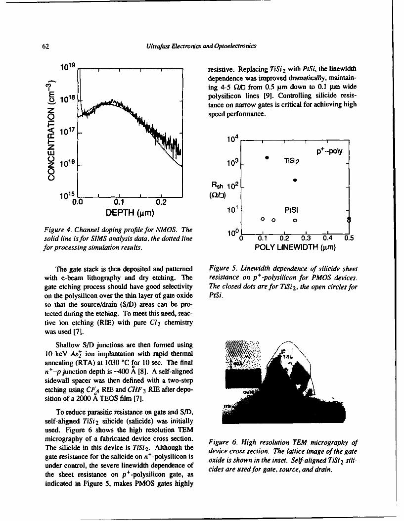
62 Ultrafast Electronics and Optoelectronics
1019 T r resistive. Replacing TiSi 2 with PtSi, the linewidth
dependence was improved dramatically, maintain-
C? ing 4-5 QAJ from 0.5 gim down to 0.1 gim wideEo 1018 polysilicon lines [9]. Controlling silicide resis-
tance on narrow gates is critical for achieving higho speed performance.0- 1017c 104, ,
zop÷-polyS1016 103 TiSi2
00
Rsh 1021015 (Li/tJ)
0.0 0.1 0.2DEPTH (pm) 101 PtSi
o o 0
Figure 4. Channel doping profile for NMOS. The 100 'solid line is for SIMS analysis data, the dotted line 0 0.1 0.2 0.3 0.4 0.5for processing simulation results. POLY LINEWIDTH (gim)
The gate stack is then deposited and patterned Figure 5. Linewidth dependence of silicide sheetwith e-beam lithography and dry etching. The resistance on p+-polysilicon for PMOS devices.gate etching process should have good selectivity The closed dots are for TiSi2 , the open circles foron the polysilicon over the thin layer of gate oxide PtSi.so that the source/drain (S/D) areas can be pro-tected during the etching. To meet this need, reac-tive ion etching (RIE) with pure Cl 2 chemistrywas used [71.
Shallow S/D junctions are then formed using10 keV As' ion implantation with rapid thermal -annealing (RTA) at 1030 °C for 10 sec. The final
+ 0
n+-p junction depth is -400 A [8]. A self-alignedsidewall spacer was then defined with a two-stepetching using CF04 RIE and CHF3 RIE after depo-sition of a 2000 A TEOS film [7].
To reduce parasitic resistance on gate and S/D,self-aligned TiSi 2 silicide (salicide) was initiallyused. Figure 6 shows the high resolution TEMmicrography of a fabricated device cross section. Figure 6. High resolution TEM micrography ofThe silicide in this device is TiSi 2 . Although the device cross section. The lattice image of the gategate resistance for the salicide on n+-polysilicon is oxide is shown in the inset. Sel-aligned T0 2 sili-under control, the severe linewidth dependence of cides are usedfor gate, source, and drain.the sheet resistance on p+-polysilicon gate, asindicated in Figure 5, makes PMOS gates highly
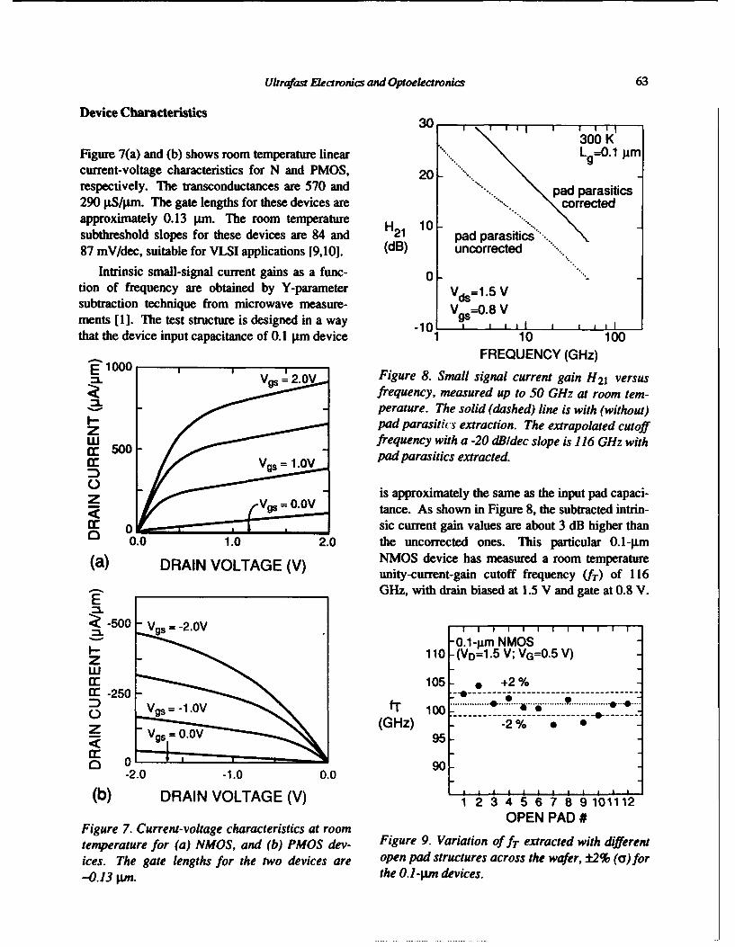
Ultrafast Electronics and Optoelectronics 63
Device Characteristics30
31300 KFigure 7(a) and (b) shows room temperature linear Lg=0.I jmcurrent-voltage characteristics for N and PMOS, 20 "respectively. The transconductances are 570 and _ p" "-... • pad parasitics
290 tLS/pm. The gate lengths for these devices are ".. correctedapproximately 0.13 ira. The room temperaturesubthreshold slopes for these devices are 84 and H21 pad parasitics...87 mV/dec, suitable for VLSI applications [9,10]. (dB) uncorrected
Intrinsic small-signal current gains as a func- 0"tion of frequency are obtained by Y-parameter Vds=1.5 Vsubtraction technique from microwave measure- V =0.8 Vments [1]. The test structure is designed in a way -10 I S ,that the device input capacitance of 0.1 tun device 1 10 100
FREQUENCY (GHz)
" 10 V-- 2.0V Figure 8. Small signal current gain H 21 versusZ /frequency, measured up to 50 GHz at room tem-= perature. The solid (dashed) line is with (without)
I-. pad parasitics extraction. The extrapolated cutoffzW frequency with a -20 dBldec slope is 116 GHz withCr 500 pad parasitics extracted.
is approximately the same as the input pad capaci-SV•_V .0...v,. tance. As shown in Figure 8, the subtracted intrin-cr 0 sic current gain values are about 3 dB higher than
0.0 1.0 2.0 the uncorrected ones. This particular 0.1-pim)DRAIN VOLTAGE (V) NMOS device has measured a room temperature(a) Dunity-current-gain cutoff frequency (fr) of 116
_ _-_GHz, with drain biased at 1.5 V and gate at 0.8 V.
Z-500 Vg -2.OV"-0.1-1±m NMOS
110 (VD=1.5 V; VG--0.5 V)Z
r" 105 * +2%CE -250 ----------------------------
Vg =)10 fT 10o -_ .............. .... ..... ..ý... .. 6-4 ..... * .9.'* ............... .....- ._
z ,,- Vg (GHz) 0 . -2% 0 .
<O 95
0 0 90-2.0 -1.0 0.0
(b) DRAIN VOLTAGE (V) 1 2 3 4 5 6 7 8 9 101112
OPEN PAD #Figure 7. Current-voltage characteristics at roomtemperature for (a) NMOS, and (b) PMOS dev- Figure 9. Variation of fT extracted with differentices. The gate lengths for the two devices are open pad structures across the wafer, ±2% ((y)for-0.13 pm. the 0.1-pim devices.
64 Ultrafast Electronics and Optoelectronics
The error margins associated with this Y- Microwave/Digital CMOS/SOS Technol-
parameter subtraction technique is established to ogy", IEEE Electron Device Lett., 12, pp.
be ±2% for 0.1-jim devices by comparing the 16-17, Jan. 1991.extracted fT values over a 2.4 cmx2.4 cm e-beam [4] M. Nanba, et al., "A 64GHz Si Bipolarwritten area. These fT values are shown in Figure Transistor Using In-Situ Phosphorus9. As summarized in Figure 1, the 0.13-jim Doped Polysilicon Emitter Technology"PMOS has measured anfT of 51 GHz [9]. IEDM Tech. Dig., 1991, pp. 443-446.
[5] G. L.- Patton, et al., "75-GHz fT SiGe-BaseAcknowledgments Heterojunction Bipolar Transistors", IEEE
Electron Device Lett., 11, pp. 171-173,
The authors would like to acknowledge the contri- Apr. 1990.
butions of G. M. Chin, M. D. Morris, R. W. John- [6] R. H. Yan, et al., "Scaling the Si MOSFET
son, K. Early, M. R. Pinto, C. S. Rafferty, M. D. into the 0.1-jim Regime Using Vertical
Feuer, and L. Manchanda, and the support of A. Doping Engineering", Appl. Phys. Lett.,
Ourmazd, A. M. Voshchenkov, R. G. Swartz, J. 59, pp.3315-3317, Dec. 1991.
Bokor, and R. E. Howard. [7] D. Y. Jeon, et al., "Gate Technology for 89GHz Vertical Doping Engineered Si MOS-FET", J. Vac. Sci. Technol., 10, pp.2922-
References 2926, Nov/Dec 1992.[81 B. G. Park, et al., "Ultrashallow Junctions
for ULSI Using As' Implantation and[11 R. H. Yan, et al., "89-GHz fT Room- Rapid Thermal Anneal", IEEE Electron
Temperature Silicon MOSFET's", IEEE Device Lett., 13, pp. 507-509, Oct. 1992.Electron Device Lett., 13, pp. 256-258, [9] K. F. Lee, et al., "0.1 jim P-Channel MOS-May. 1992. FETs with 51 GHz fT", IEDM Tech. Dig.,
[2] C. Raynaud, et al., "High-Frequency Per- 1992, pp. 1012-1014.formance of Submicrometer Channel- [101 R. H. Yan, et al., "High Performance 0.1-Length Silicon MOSFETs", IEEE Electron jim Room Temperature Si MOSFETs",Device Lett., 12, pp. 667-669, Dec. 1991. 1992 Sym. VLSI Tech. Tech. Dig., pp.86-
[31 A. E. Schmitz, et al., "A Deep Submicron 87.
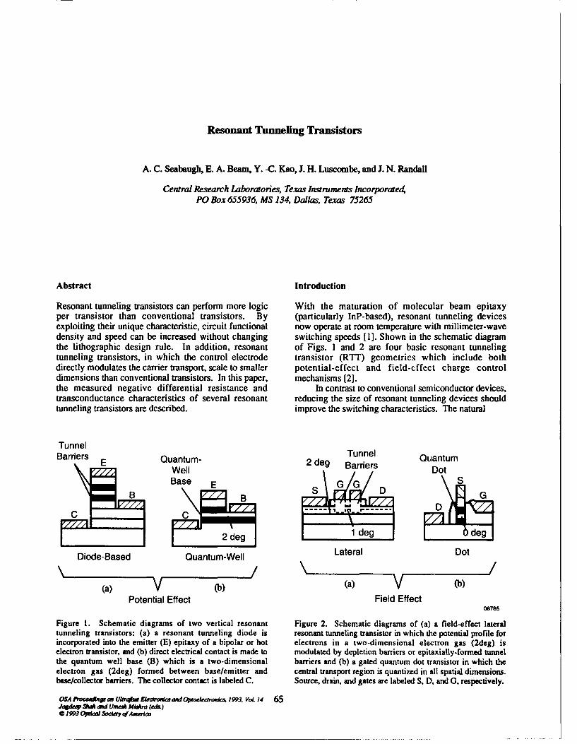
Resonant Tunneling Transistors
A. C. Seabaugh, E. A. Beam, Y. -C. Kao, J. H. Luscombe, and J. N. Randall
Central Research Laboratories, Texas Instruments IncorporatedPO Box 655936, MS 134, Dallas, Texas 75265
Abstract Introduction
Resonant tunneling transistors can perform more logic With the maturation of molecular beam epitaxyper transistor than conventional transistors. By (particularly InP-based), resonant tunneling devicesexploiting their unique characteristic, circuit functional now operate at room temperature with millimeter-wavedensity and speed can be increased without changing switching speeds [1]. Shown in the schematic diagramthe lithographic design rule. In addition, resonant of Figs. 1 and 2 are four basic resonant tunnelingtunneling transistors, in which the control electrode transistor (RTT) geometries which include bothdirectly modulates the carrier transport, scale to smaller potential-effect and field-effect charge controldimensions than conventional transistors. In this paper, mechanisms [2].the measured negative differential resistance and In contrast to conventional semiconductor devices,transconductance characteristics of several resonant reducing the size of resonant tunneling devices shouldtunneling transistors are described. improve the switching characteristics. The natural
TunnelBarriers Tunnel Quantum
E Quantum- 2 deg Barrierswell iESDot
Base EG&B BG
C .
f712 deg 1 d egde
Diode-Based Quantum-Well Lateral Dot
(a) (b) (a) (b)
Potential Effect Field Effect06785
Figure 1. Schematic diagrams of two vertical resonant Figure 2. Schematic diagrams of (a) a field-effect lateraltunneling transistors: (a) a resonant tunneling diode is resonant tunneling transistor in which the potential profile forincorporated into the emitter (E) epitaxy of a bipolar or hot electrons in a two-dimensional electron gas (2deg) iselectron transistor, and (b) direct electrical contact is made to modulated by depletion barriers or epitaxially-formed tunnelthe quantum well base (B) which is a two-dimensional barriers and (b) a gated quantum dot transistor in which theelectron gas (2deg) formed between base/emitter and central transport region is quantized in all spatial dimensions.base/collector barriers. The collector contact is labeled C. Source, drain, and gates are labeled S, D, and G, respectively.
OSA Proces*xg on Ukrqlbw EkCfr dc and OpXoetroja 1993, Vol. 14 65JqdaVp i amd Umues M"ma (ed&)* 1993 Opdcat Sockey afAmmia
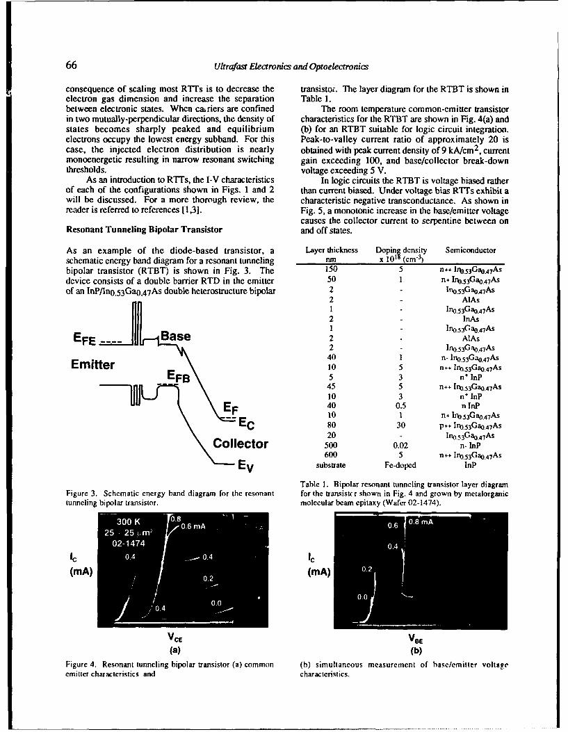
66 Ultrafast Electronics and Optoelectronics
consequence of scaling most RTTs is to decrease the transistoi. The layer diagram for the RTBT is shown inelectron gas dimension and increase the separation Table 1.between electronic states. When cariers are confined The room temperature common-emitter transistorin two mutually-perpendicular directions, the density of characteristics for the RTBT are shown in Fig. 4(a) andstates becomes sharply peaked and equilibrium (b) for an RTBT suitable for logic circuit integration.electrons occupy the lowest energy subband. For this Peak-to-valley current ratio of approximately 20 iscase, the injected electron distribution is nearly obtained with peak current density of 9 kA/cm 2 , currentmonoenergetic resulting in narrow resonant switching gain exceeding 100, and base/collector break-downthresholds. voltage exceeding 5 V.
As an introduction to RTTs, the I-V characteristics In logic circuits the RTBT is voltage biased ratherof each of the configurations shown in Figs. I and 2 than current biased. Under voltage bias RTTs exhibit awill be discussed. For a more thorough review, the characteristic negative transconductance. As shown inreader is referred to references [1,3]. Fig. 5, a monotonic increase in the base/emitter voltage
causes the collector current to serpentine between onResonant Tunneling Bipolar Transistor and off states.
As an example of the diode-based transistor, a Layer thickness Doping density Semiconductorschematic energy band diagram for a resonant tunneling nm x 10i (cm3)bipolar transistor (RTBT) is shown in Fig. 3. The 150 5 n++ Ib.53GaO. 47Asdevice consists of a double barrier RTD in the emitter 50 1 n+ InO.53GaO.47Asof an InP/InO.53GaO.4 7 As double heterostructure bipolar 2 - lno.53Ga 0 .4 7 As
2 - AlAsI - Ino.53Gao.47As2 - InAs1 - Ino 53Gao 47As
EFE Base 2 - AlAs2 - Ino.53Gao.47As40 1 n- lno.53Gao.47As
Emitter 10 5 n++ In .53Ga ,47AsE B5 3 n+ lnP
45 5 n++ ln0.53Gao.47 As10 3 n÷ InP
EF 40 0.5 n InPEF 10 1 n+ 1P. 5 3Ga0.4 7 AsEC 80 30 p++ Ino.53Gao.47As
20 - In0.53Ga0 .47AsCollector 5oo 0.02 n- InP
600 5 n++ In0.53Gao.47AsEv substrate Fe-doped lnP
Table 1. Bipolar resonant tunneling transistor layer diagramFigure 3. Schematic energy band diagram for the resonant for the transistcr shown in Fig. 4 and grown by metalorganictunneling bipolar transistor. molecular beam epitaxy (Wafer 02-1474).
25. - 25I urn 2 t'' ''•'
Ic 0.4 0.4 Ic
(mA) 0. (mA)
VCE VBE
(a) (b)Figure 4. Resonant tunneling bipolar transistor (a) common (h) simultaneous measurement of base/emitter voltageemitter characteristics and characteristics.
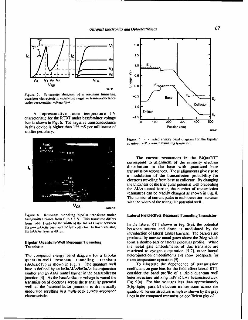
Ultrafast Electronics and Oproelectronics 67
V E V 1 12.0
IC IC 1.5- - -- -V 3
-V1.0 EFES- - V2 ---- - --- .
V0 V1 V2 V3 VCECBEVBE w 0.0 FB
08784
Figure 5. Schematic diagram of a resonant tunnelingtransistor characteristic exhibiting negative transconductance Ecunder base/emitter voltage bias. Co
-1.0 Collector
A representative room temperature I-VEmitter E,characteristic for the RTBT under base/emitter voltage -1.5
bias is shown in Fig. 6. The negative transconductance 0 100 200 300 400 500
in this device is higher than 125 mS per millimeter of Position (nm)emitter periphery. 06746
Figure 'i ' ,uted energy band diagram for the bipolarquantum--vcl! 4 ,.onant tunneling transistor.
The current resonances in the BiQuaRTTcorrespond to alignment of the minority electron
IC "distribution in the base with quantized basetransmission resonances. These alignments give rise toa modulation of the transmission probability forelectrons traveling from base to collector. By changing
1.0 the thickness of the triangular potential well preceedingthe AlAs tunnel barrier, the number of transmission
0.4_ resonances can be readily changed as shown in Fig. 8.0.2 The number of current peaks in each transistor increases
7.0.0 with the width of the triangular potential well.VCE 00787.2
Figure 6. Resonant tunneling bipolar transistor under Lateral Field-Effect Resonant Tunneling Transistorbase/emitter biases from 0 to 1.8 V. This transistor differsfrom Table 1 only by the width of the InGaAs layer between In the lateral RTT shown in Fig. 2(a), the potentialthe p'-- InGaAs base and the InP collector. In this transistor, between source and drain is modulated by thethe InGaAs layer is 40 Tun. introduction of lateral tunnel barriers. The barriers are
produced by narrow metal gates above the 2deg whichBipolar Quantum-Well Resonant Tunneling form a double-barrier lateral potential profile. WhileTransistor the metal gate embodiments of this transistor are
restricted to cyogenic operation [5-7], other lateralThe computed energy band diagram for a bipolar heterojunction embodiments 18] show prospects forquantum-well resonant tunneling transistor room temperature operation [9].(BiQuaRTT) is shown in Fig. 7. The quantum well To illustrate the dependence of transmissionbase is defined by an lnGaAlAs/InGaAs heterojunction coefficient on gate bias for the field-effect lateral RTr,emitter and an AlAs tunnel barrier in the base/collector consider the band profile of a triple quantum welljunction [4]. As the base/collector voltage is varied the heterostructure utilizing InP/InGaAs hcterostructures,transmission of electrons across the triangular potential Fig. 9(a). For bias voltages less than approximatelywell at the base/collector junction is dramatically 2(EF-EO)/q, parallel electron transmission across themodulated resulting in a multi-peak current-resonance quadruple barrier structure is high as shown by the graycharacteristic, lines in the computed transmission coefficient plot of
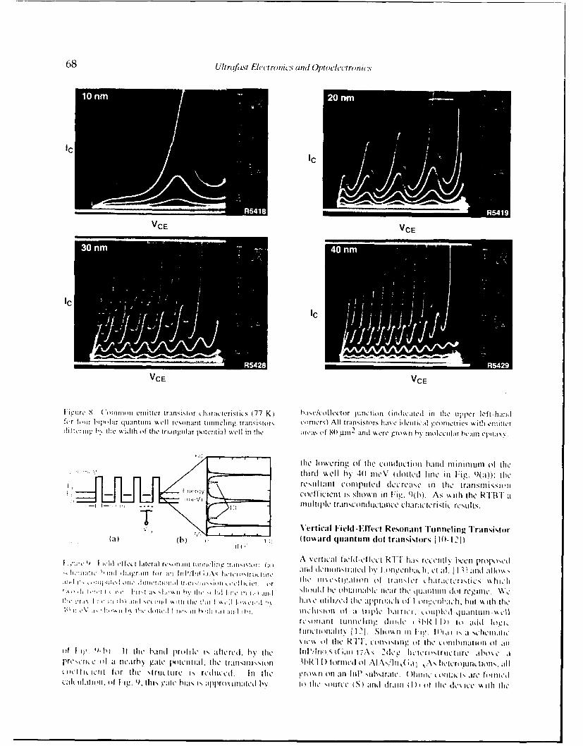
68 Ultra /',Ls Electronic., and OptovlectroniC.1
I 0
ICC
IIC
VICE VCE
Figure S. (Cnnomm enlitter transistor dharacterl stics (77 K) ha,,e/ctllettor junction Ii(ic~itedk inl the upper left-hand1for four bipolar quantum wkell resonant nelTUIntTdntr corner;) All transistors have ideritiCýIl !CeOnIetries; With em1itterTdifitrilig I,% the width oflthe triangtilar potentliall well in the areaS (If S() pm,2 Mid wereT gressrt h\ 1110t'LecTtr beaM1 ep)1Iras
Ifhe lowerjniz of' rthe conduction baiti minitmumi of- thethtird well 1wy 4(0 Itev (dotted flirt ill [-i. 9(a)): Itheresultant tintptited decreasec inl the transmissýIon1
Ivctoellic jent is shown in Figi. 90)l'. As with the RUHIO aintiplet pIran scrd m c tance chta ra cterFistic re sLtIIt.
Vertical Field-EfTect Resonant Tusnneling Transistor()(h) IT I,' ard qujantum (lot transistors I1W- 121
~i cl efectlitralresrtmir iiuulitg ranistr:A vertical ficld-ClItcC ilT itAs recLeiitl\ bccii lroposediind diennirtmtritd hv I .~lteeuix, 11t al . I 'I and alloshhmiind dioiluarmn fbr 11 lnl'/Irit .tA`I hCL'T0`trostru1ti
.ii :- ~i::t.!one '1iittientiti.l ri11 ~ 'itli i r It t esltt'tt ll of 1rattsler titAraclerislics \%hiti~l
h I!',' iii1 01:1 .IT) 1:1 ti .'O11 ýjj 111C ",10 1 fl hJ~ Wi tili,'d Ific aplirimaci of I hiteta i ll b kti t Owit ttVtr 'V lio, 1 Ikn b\ the litte11cl ITS ! m . 1~t
'.1; tttctIsb). of a titple bairItr, ollettaoiwircsona~nt ttttieittn dtode bI< Ih 11) lo add lop,~
)i f itt te RN1'1 colpnsusine of [tiecitbiaotot.iMh I tI 'v,9)),~ It tlit handt prittile i', altered IN t11C lI'IltIIIttS1 ifai 7As NCLee lieterostirnti~lre abose aprectt.~n c 1o1 a necirbt gate ptenimal . (thc transrtissott ;hRI I)D orined Of A~/1 5 ;J j lieteroltmincDons,. allutifl i. tet for Owt Atrmtitire is rcilticd. In itie ero' it onl anl fil) iitibsmtra. ( )himiik cottla Vs arc fowittlcalk tilattort of f ig. 9, thil, eval bias, is approxitnated hw to Ithe otirLc (S) and dr.itt 11) 1of tire dc% ice v. itli tlte
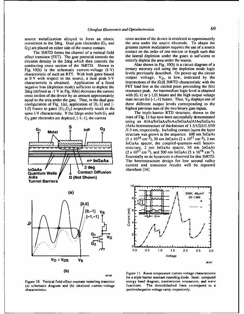
Ultrafast Electronics and Optoelectronics 69
source metallization alloyed to form an ohmic cross section of the device is restricted to approximatelyconnection to the 2deg. Dual gate electrodes (G1 and the area under the source electrode. To obtain theG2 ) are placed on either side of the source contact. greatest current modulation requires the use of a source
The 3bRTD forms the channel of a vertical field contact on the order of one micron in length such thateffect transistor (FET). The gate potential controls the the lateral depletion under the gates is sufficient toelectron density in the 2deg which then controls the entirely deplete the area under the source.conducting cross section of the 3bRTD. Shown in Also shown in Fig. 10(b) is a circuit diagram of aFig. 10(b) is the schematic current-voltage (I-V) ternary memory cell using the depletion mode logiccharacteristic of such an RTT. With both gates biased levels previously described. On power-up the circuitat 0 V with respect to the source, a dual peak I-V output voltage, Vo, is low, indicated by thecharacteristic is obtained. Application of a fixed intersections of the [0,0] 3bRTD characteristic with thenegative bias (depletion mode) sufficient to deplete the FET load line at the circled point preceeding the first2deg (defined as -1 V in Fig. 9(b)) decreases the current resonance peak. An intermediate logic level is obtainedcross section of the device by an amount approximately with [0,-l1 or [-1,01 biases and the high output voltageequal to the area under the gate. Thus, in the dual gate state occurs for [-1,-1] biases. Thus, Vo displays one ofconfiguration of Fig. 1(a), application of [0,-i] and [- three different output levels corresponding to the1,0] biases to gates [G 1,G21 respectively result in the highest previous sum of the two binary gate inputs.same I-V characteristic. If the 2degs under both GI and The triple-barrier RTD structure, shown in theG2 gate electrodes are depleted, [-1,-1], the current inset of Fig. 11 has now been successfully demonstrated
using an AIAs/InGaAs/InAsllnGaAs/AIAs/InGaAsS /AlAs heterostructure of thicknesses of 1.5/1/2/1/1.5/10
G1 Metal InP G2 /1.5 nm, respectively. Including contact layers the layerMetalstructure was grown in the sequence: 600 nm InGaAs
(5 x 1018 cm-3 ), 50 nm InGaAs (2 x 1017 cm-3 ), 2 nmInGaAs spacer, the coupled-quantum-well hetero-structure, 2 nm InGaAs spacer, 50 nm InGaAs(2 x 1017 cm- 3 ), and 300 nm InGaAs (5 x 1018 cm-3).Essentially no dc hysteresis is observed for this 3bRTD.
n+ InGaAs The heterostructure design for low second valleyInGaAs 2 deg current and transistor results will be reported
Quantum Wells Contact Diffusion elsewhere [14].AlAs D (Not Shown)Tunnel Barriers
10 .................. .....I......I.....I.....I.....I....
(a) 300K, 48pm 2
8 02-1368
[0,0]1u06 - . .....e[0,-1 VSE 6i
2 2n
0-I/" ,'
/ ". 0.0 0.5 1.0 1.5 2.0 2.5 3.0
Voltage
VO =VDS Vs 0878
(b) 0878 Figure 11. Room temperature current-voltage characteristics
for a triple barrier resonant tunneling diode. Inset: computedFigure 10. Vertical field-effect resonant tunneling transistor energy band diagram, transmission resonances, and wave(a) schematic diagram and (b) idealized current-voltage functions. The dotted/dashed lines correspond to acharacteristics, positive/negative voltage ramp, respectively.
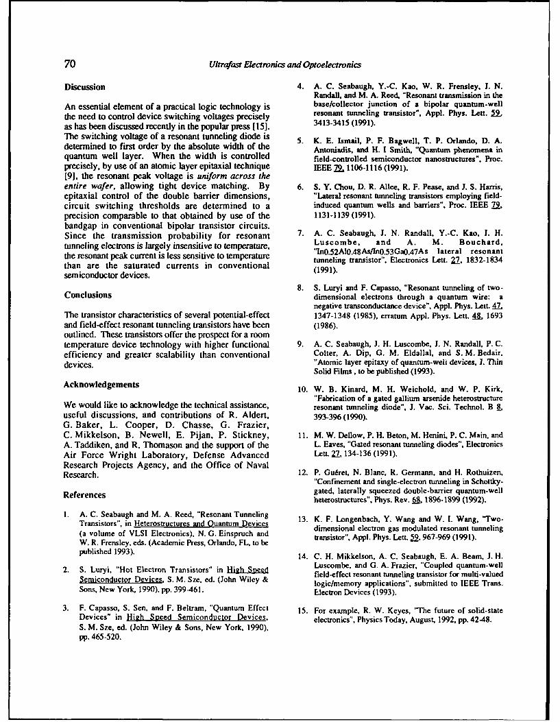
70 Ultrafast Electronics and Optoelectronics
Discussion 4. A. C. Seabaugh. Y.-C. Kao, W. R. Frensley, J. N.Randall, and M. A. Reed, "Resonant transmission in the
An essential element of a practical logic technology is base/collector junction of a bipolar quantum-well
the need to control device switching voltages precisely resonant tunneling transistor". Appl. Phys. Lett. aas has been discussed recently in the popular press [15]. 3413-3415 (1991).
The switching voltage of a resonant tunneling diode is 5. K. E. Ismail, P. F. Bagwell, T. P. Orlando, D. A.determined to first order by the absolute width of the Antoniadis, and H. I Smith, "Quantum phenomena inquantum well layer. When the width is controlled field-controlled semiconductor nanostructures", Proc.precisely, by use of an atomic layer epitaxial technique IEEE 79. 1106-1116 (1991).[91, the resonant peak voltage is uniform across theentire wafer, allowing tight device matching. By 6. S. Y. Chou, D. R. Allee, R. F. Pease, and J. S. Harris,epitaxial control of the double barrier dimensions, "Lateral resonant tunneling transistors employing field-circuit switching thresholds are determined to a induced quantum wells and barriers", Proc. IEEE 2.precision comparable to that obtained by use of the 1131-1139 (1991).bandgap in conventional bipolar transistor circuits.Since the transmission probability for resonant 7. A. C. Seabaugh, J. N. Randall, Y.-C. Kao, J. H.
tunneling electrons is largely insensitive to temperature, Luscombe, and A. M. Bouchard,
the resonant peak current is less sensitive to temperature tunn.52Al0g48As/Ino.53Ga0.47As lateral resonant
than are the saturated currents in conventional (1991).
semiconductor devices. (1991).
8. S. Luryi and F. Capasso, "Resonant tunneling of two-Conclusions dimensional electrons through a quantum wire: a
negative transconductance device", Appl. Phys. Lett. 427The transistor characteristics of several potential-effect 1347-1348 (1985), erratum Appl. Phys. Lett. 4L 1693and field-effect resonant tunneling transistors have been (1986).outlined. These transistors offer the prospect for a roomtemperature device technology with higher functional 9. A. C. Seabaugh, J. H. Luscombe, J. N. Randall, P. C.efficiency and greater scalability than conventional Colter, A. Dip, G. M. Eldallal, and S. M. Bedair,
devices. "Atomic layer epitaxy of quantum-weli devices, J. ThinSolid Films, to be published (1993).
Acknowledgements 10. W. B. Kinard, M. H. Weichold, and W. P. Kirk,
"Fabrication of a gated gallium arsenide heterostructureWe would like to acknowledge the technical assistance, resonant tunneling diode", J. Vac. Sci. Technol. B .Iuseful discussions, and contributions of R. Aldert, 393-396 (1990).G. Baker, L. Cooper, D. Chasse, G. Frazier,C. Mikkelson, B. Newell, E. Pijan, P. Stickney, 11. M. W. Dellow, P. H. Beton, M. Henini, P. C. Main, andA. Taddiken, and R. Thomason and the support of the L. Eaves, "Gated resonant tunneling diodes". ElectronicsAir Force Wright Laboratory, Defense Advanced Lett. 27, 134-136 (1991).Research Projects Agency, and the Office of NavalResearch. 12. P. Gufret, N. Blanc, R. Germann, and H. Rothuizen,
"Confinement and single-electron tunneling in Schottky-
References gated, laterally squeezed double-barrier quantum-wellheterostructures", Phys. Rev. 68, 1896-1899 (1992).
1. A. C. Seabaugh and M. A. Reed, "Resonant Tunneling 13. K. F. Longenbach, Y. Wang and W. I. Wang, "Two-Transistors", in Heterostructures and Ouantum Devices dimensional electron gas modulated resonant tunneling(a volume of VLSI Electronics), N. G. Einspruch and transistor", Appl. Phys. Lett. 5mut967-969 (1991).W. R. Frensley, eds. (Academic Press, Orlando, FL, to bepublished 1993). 14. C. H. Mikkelson, A. C. Seabaugh, E. A. Beam, J. H.
2. S. Luryi, "Hot Electron Transistors" in Hh Luscombe, and G. A. Frazier, "Coupled quantum-well2.Se ic"onducotors DevicesS.M.Szeed.(John Wilheey &field-effect resonant tunneling transistor for multi-valuedSemiconductor" Devices, S. M. Sze, ed. (John Wiley & logic/memory applications", submitted to IEEE Trans.Sons, New York, 1990). pp. 399-461. Electron Devices (1993).
3. F. Capasso, S. Sen. and F. Beltram, "Quantum Effect 15. For example, R. W. Keyes, "'he future of solid-stateDevices" in High Speed Semiconductor Devices, electronics", Physics Today, August, 1992, pp. 4248.S. M. Sze, ed. (John Wiley & Sons, New York, 1990),pp. 465-520.
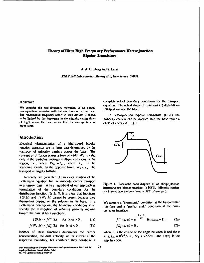
Theory of Ultra High Frequency Performane HeterojunctionBipolar Transistors
A. A. Grinberg and S. Luryi
AT&TBeU Laboratories, Murray Hill, New Jersey 07974
Abstract complete set of boundary conditions for the transport
We consider the high-frequency operation of an abrupt- eiquation. The actual shape of functions (1) depends on
heterojunction transistor with ballistic transport in the base. ransport outside the base.The fundamental frequency cutoff in such devices is shown In heterojunction bipolar transistors (HBT) theto be limited by the dispersion in the minority-carrier times minority carriers can be injected into the base "over aof flight across the base, rather than the average time of cliff" of energy A, Fig. 1:flight itself.
IntroductionElectrical characteristics of a high-speed bipolarjunction transistor are in large part determined by the ..............uar-port of minority carriers across the base. Theconcept of diffusion across a base of width WB is validonly if the particles undergo multiple collisions in theregion, i.e., when W1, ý- l€, where l1. is thescattering length. In the opposite limit, W 5 s < 1,,, thetransport is largely ballistic.
Recently, we presented [1] an exact solution of theBoltzmann equation for the minority carrier transportin a narrow base. A key ingredient of our approach is Figure 1. Schematic band diagram of an abrupt-junctiononuaon ofarrowbase.Ake y conre dientions fr a h i heterostructure bipolar transistor (a-HBT). Minority carriersform ulation of the boundary co nditions for the aeij ce n ot eb s o e l f "o n r y A
distribution function f(r, k, t). It is clear that functions are injected into the base "over a cliff" of energy A.f(0, k) and f((WB. k) cannot be preset, because theythemselves depend on the solution in the base. In a We assume a "thermionic" condition at the base-emitterBoltzmann description, the boundary conditions must interface and a "perfect sink" condition at the base-specify the distribution of inbound particles moving collector interface:toward the base at both junctions, E1,-A
f(0, k) =- fg+) (k) for k.i>0; (la) fg+) (k, u) = e kT e(uk/ko-- 1) (2a)
f(Wa,k)-fk-a (k) for k.i<0. (lb) fk-) (ku)=0, (2b)
Neither of these functions determines the carrier where u is the cosine of the angle between k and the zconcentration, the drift velocity, or the current at the axis, Ek S A2 k2 /2m. Ak0 r 4Al/2m, and O(x) is therespective boundary, but combined they constitute a step function.
OSA P'ocea~bp on Wgn$,5 frooeks asd Opo¢elcoeim 1993. VoL 14 71Jadeep -' and Une, MOW (e&)0 1993 Optical Sockwp efAnwria
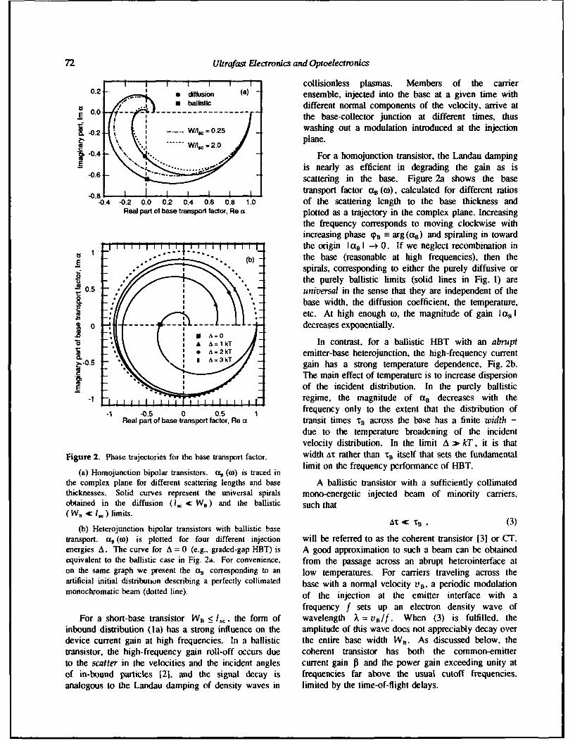
72 Ultrafast Electronics and Optoelectronics
II I collisionless plasmas. Members of the carrier0.2 * • aflusion (a) ensemble, injected into the base at a given time with
- ballsic different normal components of the velocity, arrive at- 0 - the base-collector junction at different times, thus1-02 ..... = 0.25 washing out a modulation introduced at the injection
"plane.-0.4 -For a homojunction transistor, the Landau damping
-- ............ is nearly as efficient in degrading the gain as is-0.6 -• scattering in the base. Figure 2a shows the base
-0.8 transport factor %B ((o), calculated for different ratios-0.4 -0.2 0.0 0.2 0.4 0.6 0.8 1.0 of the scattering length to the base thickness and
Real part of base transport factor, Re cc plotted as a trajectory in the complex plane. Increasingthe frequency corresponds to moving clockwise withincreasing phase TB =- arg(at) and spiraling in toward
1 11.....I Ithe origin Ia. 1 -- 0. If we neglect recombination in
"E .(b) the base (reasonable at high frequencies), then the_ Ispirals, corresponding to either the purely diffusive or-0
0 the purely ballistic limits (solid lines in Fig. 1) areS0.5 , universal in the sense that they are independent of the
* base width, the diffusion coefficient, the temperature,etc. At high enough co, the magnitude of gain I a, I
0 ---- ----------------- decreases exponentially." A= 1 kT In contrast, for a ballistic HBT with an abrupt-0.A == 3 kT emitter-base heterojunction, the high-frequency current
gain has a strong temperature dependence, Fig. 2b.The main effect of temperature is to increase dispersion
E_, of the incident distribution. In the purely ballistic-1 • regime, the magnitude of caB decreases with the
-1 -0.5 0 0.5 1 frequency only to the extent that the distribution ofReal part of base transport factor, Re a transit times T. across the base has a finite width -
due to the temperature broadening of the incidentvelocity distribution. In the limit A >x kT, it is that
Figure 2. Phase trajectories for the base transport factor, width At rather than TB itself that sets the fundamentallimit on the frequency performance of HIBT.
(a) Homojunction bipolar transistors. %, (ro) is traced in
the complex plane for different scattering lengths and base A ballistic transistor with a sufficiently collimatedthicknesses. Solid curves represent the universal spirals mono-energetic injected beam of minority carriers.obtained in the diffusion (I. < W9) and the ballistic such that(W, C I= ) limits.
(b) Heterojunction bipolar transistors with ballistic base (3)
transport. N, (w) is plotted for four different injection will be referred to as the coherent transistor [3] or CT.energies A. The curve for A = 0 (e.g., graded-gap HBT) is A good approximation to such a beam can be obtainedequivalent to the ballistic case in Fig. 2a. For convenience, from the passage across an abrupt heterointerface aton the same graph we present the a, corresponding to an low temperatures. For carriers traveling across theartificial initial distribution describing a perfectly collimated base with a normal velocity vB, a periodic modulationmonochromatic beam (dotted line), of the injection at the emitter interface with a
frequency f sets up an electron density wave ofFor a short-base transistor WB !5 1, the form of wavelength X = vB/f. When (3) is fulfilled, the
inbound distribution (la) has a strong influence on the amplitude of this wave does not appreciably decay overdevice current gain at high frequencies. In a ballistic the entire base width W9. As discussed below, thetransistor, the high-frequency gain roll-off occurs due coherent transistor has both the common-emitterto the scatter in the velocities and the incident angles current gain 0 and the power gain exceeding unity atof in-bound particles [21. and the signal decay is frequencies far above the usual cutoff frequencies.analogous to the Landau damping of density waves in limited by the time-of-flight delays.
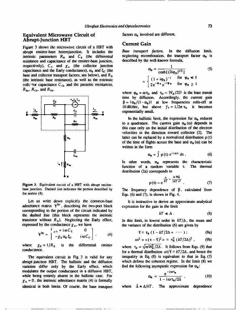
Ultrafast Electronics and Optoelectronics 73
Equivalent Microwave Circuit of factors aB involved are different.Abrupt-Junction HBT Current Gain
Figure 3 shows the microwave circuit of a HBT withabrupt emitter-base heterojunction. It includes the Base transport factors. In the diffusion limit,intrinsic parameters RE and Ce (the differential neglecting recombination, the transport factor % isresistance and capacitance of the emitter-base junction, described by the well-known formula,respectively), Cc and g, (the collector junction Icapacitance and the Early conductance), aB and 4 (the . cosh [(2i=)) 2] (5)
base and collector transport factors, see below), and R1 c
(the intrinsic base resistance), as well as the extrinsic = (1 + iiB )-I for (PR ýc 1
colft-or capacitance Cc, and the parasitic resistances, 2 e2e-•S e-i'9 for TB > 1R•, Rc•, and R~x. where 9PB = cotD and CD = WB/2D is the base transit
time by diffusion. Accordingly, the current gaini= 1a/(1--t)I at low frequencies rolls-off at
10dB/dec, but above fT = l/2ir nD it becomesE - c exponentially small.
"R- Rg Re. In the ballistic limit, the expression for ao reducesVA to a quadrature. The current gain %, (w) depends in
this case only on the initial distribution of the electronvelocities in the direction toward collector [2]. The
.R latter can be replaced by a normalized distribution p (T)of the time of flights across the base and cxB (w) can bewritten in the form
cx rB = Jp(t) eC d&. (6)In other words, za represents the characteristicfunction of a random variable t. The thermaldistribution (2a) corresponds to
A A mW121
Figure 3. Equivalent circuit of a HIBT with abrupt emitter- P (@) = e T 2kT ' (7)
base junction. Dashed line indicates the portion described by The frequency dependence of I], calculated fromthe matrix (4). Eqs. (6) and (7), is shown in Fig. 4.
Let us write down explicitly the common-base It is instructive to derive an approximate analyticaladmittance matrix ybi, describing the two-port block expression for the gain in the limitcorresponding to the portion of the circuit indicated by U A (8)the dashed line (this block represents the intrinsictransistor without RB). Neglecting the Early effect, In this limit, to lowest order in kT/A, the mean andexpressed by the conductance g A, we have the variance of the distribution (6) are given by
ybi + []C 0 (4 T TB ( I - kT/2A + • • - ) ; (9a)
tATz -- <(,,-_ )2> = B2 (kT/2 )2,& (9b)
where gE =_ I/RE is the differential emitter where c, a- 4mW•mWNB/2A. It follows from Eqs. (9) thatconductance. for a thermal distribution Arc/ = kT/2A, and hence the
The equivalent circuit in Fig. 3 is valid for any inequality in Eq. (8) is equivalent to that in Eq. (3)abrupt-junction HBT. The ballistic and the diffusion which defines the coherent regime. In the limit (8) wevarieties differ only by the Early effect, which find the following asymptotic expression for ctB:modulates the output conductance in a diffusive HBT, -i xswhile being entirely absent in the ballistic case. For cr9 (10)9A= 0, the intrinsic admittance matrix (4) is formally 1 - iO3T/2Aidentical in both limits. Of course, the base transport where A B A/kT. The approximate dependence
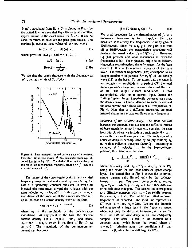
74 Ultrafas Electronics and Optoelectronics
2 (w), calculated from Eq. (10) is plotted in Fig. 4 by 0 = 1 2sin(oTB /2) 1-' (14)
the dotted line. We see that Eq. (10) gives an excellentapproximation to the exact result for a = 5. It can be The usual procedure for the determination of f d in aused, therefore, to calculate the peak gain values. The microwave transistor is to extrapolate the datamaxima Ov, occur at those values of w = ox, where measured at relatively low frequencies to unity gain at10dB/decade. Since for WtBx <_ 1, the gain (14) rolls
Im(a) = 0 *R.•(a) >0, (Ili off at 10dB/decade, the extrapolation procedure willwhich gives for wOAX< 1 and v = 1, 2, • produce the usual value fT = 1/(2n TB). However,
Eq. (14) predicts additional resonances at extendedoxf = 2n v, (12a) frequencies (12a). Their physical origin is as follows.
2 Neglecting recombination, the only reason for the base2 (12b) current to flow is to maintain neutrality of the base()VAT 2 layer. The resonant frequencies (12a) correspond to an
We see that the peaks decrease with the frequency as integer number v of periods A. = vBIf of the density) 2 i.e., at the rate of 20dB/dec. wave (13) in the base. To the extent that the wave is
not decaying in amplitude in a perfect CT, the total20 I minority-carrier charge in resonance does not fluctuate
at all. The output current modulation is thus•. 15 A=5kT ' accomplished with no rf current input, hence the
S40 dWdec "infinite" gain. In an imperfectly coherent transistor,C" 10 the density wave is Landau damped to some extent and
o the base current has a finite value at all frequencies, cf.5 - Fig. 4. Note that in a diffusion transistor, the total
ci injected charge in the base oscillates at any frequency.0 0
E • Inclusion of the collector delay. The stark contrast9U -5 - between the coherent ballistic and the diffusive modesEE of base transit by minority carriers, can also be seen
-10 20dBde from Fig. 5, where we include a transit angle 0 -= 1Tc-15 % across the base-collector junction. The inclusion of a
1 10 lOO collector delay is accomplished by simply multiplyingDimensionless Frequency wro axB with a collector transport factor •c. Assuming a
saturated drift velocity vs in the base-collectorjunction, this factor is of the form
Figure 4. Base transport limited current gain of a coherent e1 eietransistor. Solid line shows p2 (CO), calculated from Eq. (6), = 1 - e` sin(0)e-°'(dotted line from Eq. (10). The dashed lines indicate the gain iO o' (
roll-off in the conventional frequency range (f < fT ) and the where 0' = (o re and 'T, = 2%' = Wc/vs with W,extended range (f > I ). being the width of the base-collector space-charge
layer. The dotted line in Fig. 5 shows the common-The nature of the current-gain peaks in an extended emitter current gain, limited only by the collector
frequency range is best understood by considering the transit 'Tc = I ps. This curve corresponds to settingcase of a "perfectly" coherent transistor, in which all tI = TB = 0, which gives a, = I for either diffusiveinjected electrons travel toward the -,llector with the or ballistic base transport. The dashed line correspondssame velocity vB = (2A/m)1/ 2. In this case, a periodic to a diffusive transport with T. = 2ps (while keepingmodulation of the injection at the emitter interface sets the same rc = I ps). The cutoff has shifted to lowerup in the base an electron density wave of the form: frequencies, as expected. The solid line represents a
nz, t) n Z/B) (13) CT with "TC= lps, TB ==2ps. We see the dramaticn (z, t) = no ei(0- ), (13) reemergence of a large gain in the frequency range,
where no is the amplitude of the concentration where not only the diffusive transistor, but even themodulation. At any point in the base, the electron transistor with no base delay at all, are completelycurrent density I (z, t) equals -env, and hence damped. This effect is due to the addition of a%9 =exp(-iwt't), which is the limit of Eq. 10 as coherent delay, which boosts the overall phase ofAT- 0. The magnitude of the common-emitter a = % c , bringing about the condition (11) thatcurrent gain becomes maximizes P. while I ala is still large (= 0.7).
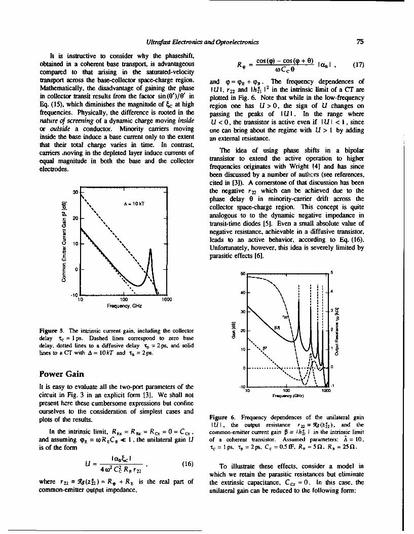
Ultrafast Electronics and Optoelectronics 75
It is instructive to consider why the phaseshift,obtained in a coherent base transport, is advantageous RT = cos(QP) - cos (Q + 0) l , (17)
compared to that arising in the saturated-velocity (0 Cc 6
transport across the base-collector space-charge region. and T = TE + TB-. The frequency dependences ofMathematically, the disadvantage of gaining the phase I UI , r22 and I h~f 12 in the intrinsic limit of a CT arein collector transit results from the factor sin (0')/0' Mi plotted in Fig. 6. Note that while in the low-frequencyEq. (15), which diminishes the magnitude of ,c at high region one has U > 0, the sign of U changes onfrequencies. Physically, the difference is rooted in the passing the peaks of I U I. In the range wherenature of screening of a dynamic charge moving inside U < 0, the transistor is active even if I U I < 1, sinceor outside a conductor. Minority carriers moving one can bring about the regime with U > 1 by addinginside the base induce a base current only to the extent an external resistance.that their total charge varies in time. In contrast,carriers .noving in the depleted layer induce currents of The idea of using phase shifts in a bipolar
equal magnitude in both the base and the collector transistor to extend the active operation to higher
electrodes. frequencies originates with Wright [41 and has sincebeen discussed by a number of authors (see references,cited in [31). A cornerstone of that discussion has been
30 the negative r22 which can be achieved due to the
A=•,10kT phase delay 0 in minority-carrier drift across theM ,collector space-charge region. This concept is quite
20 analogous to to the dynamic negative impedance in% -transit-time diodes [5]. Even a small absolute value of
% Nnegative resistance, achievable in a diffusive transistor,
10 , leads to an active behavior, according to Eq. (16).X Unfortunately, however, this idea is severely limited byE % parasitic effects [61.C %0 %E 0 %c %_ _ __ _ 5
"8% %
-10 40- 4
100000\100
Frequency, GHz30 3'
Figure 5. The intrinsic current gain, including the collector 20 2
delay "r, = I ps. Dashed lines correspond to zero basedelay, dotted lines to a diffusive delay T = 2 ps, and solid 0lines to a CT with A = lOkT and "r, = 2ps. 10 . o
...........Power Gain .... :,
It is easy to evaluate all the two-port parameters of the °o1o jcircuit in Fig. 3 in an explicit form [3]. We shall not Fr.euw,(GHz)
present here these cumbersome expressions but confineourselves to the consideration of simplest cases andplots of the results. Figure 6. Frequency dependences of the unilateral gain
IUI , the output resistance r 22• X(Z22 ), and theIn the intrinsic imit, R = =Rc = 0 = Cc, common-emitter current gain I3 -he 1 I in the intrinsic limit
and assuming qE -= wR EC E ýC 1, the unilateral gain U of a coherent transistor. Assumed parameters: A = 10.is of the form , = lps, -s = 2 ps, C, = 0.5 fF, R, = 5Q, R, = 25 0.
U aBkCI(641= , (16) To illustrate these effects, consider a model in4 C r2which we retain the parasitic resistances but eliminate
where r 22 M R(z) = R, + RE is the real part of the extrinsic capacitance, Cc. = 0. In this case, thecommon-emitter output impedance, unilateral gain can be reduced to the following form:
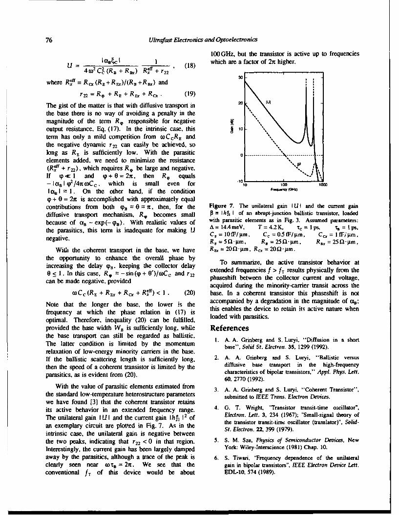
76 Ultrafast Electronics and Optoelectronics
100GHz, but the transistor is active up to frequenciesI C1BcI I which are a factor of 2n higher.U = R+R) ~+r 2 , (18)U=4 0o2C2c (Ra + RB,) Reff + r22 (8
30
where R -Rc.(RE+ R)/(R,+R,) and 3 -
r22 = RT + RE + RE, + Rc. (19)
The gist of the matter is that with diffusive transport in
the base there is no way of avoiding a penalty in themagnitude of the term R9 responsible for negative "output resistance, Eq. (17). In the intrinsic case, this 10oterm has only a mild competition from wCcRE andthe negative dynamic r 22 can easily be achieved, solong as RE is sufficiently low. With the parasitic 0......... ........ ................elements added, we need to minimize the resistance "\,0
(Reft + r 22 ), which requires RT be large and negative. "If (p < I and p+ 0=2n2, then R, equals ',-'
-10',- IBI 2/4nor)Cc, which is small even for 10 100 1000I% 1-1. On the other hand, if the condition r,•.,n ONZ
(p + 0= 2it is accomplished with approximately equalcontributions from both % = 0 = g, then, for the Figure 7. The unilateral gain I U1I and the current gaindiffusive transport mechanism, RT becomes small f=-= Ih21 I of an abrupt-junction ballistic transistor, loaded
because of aB - exp(-4PB). With realistic values of with parasitic elements as in Fig. 3. Assumed parameters:
the parasitics, this term is inadequate for making U A= 14.4meV, T = 4.2K, tc = 1 ps, ; = I ps.C, = 10fF/gm, C =0 .5fF/gm, C,= I fFi,; m,
negative. R = 5-gm, R= 25 inpm, R..= 250-tgm,
Wili the coherent transport in the base, we have Ru = 20fl-m, R,, = 200.gm.the opportunity to enhance the overall phase by To summarize, the active transistor behavior atincreasing the delay %, keeping the collector delay extended frequencies f > fT results physically from the0c< 1. In this case, Rov = -sind(9+ 0')/C and r2 phaseshift between the collector current and voltage,can be made negative, provided acquired during the minority-carrier transit across the
oCc (RE + RE, + Rc, + Reff) < 1. (20) base. In a coherent transistor this phaseshift is not
Note that the longer the base, the lower is the accompanied by a degradation in the magnitude of a0 ;
frequency at which the phase relation in (17) is this enables the device to retain its active nature when
optimal. Therefore, inequality (20) can be fulfilled, loaded with parasitics.
provided the base width WB is sufficiently long, while Referencesthe base transport can still be regarded as ballistic.The attr coditon s liite bythe ometum 1. A. A. Grinberg and S. Luryi, "Diffusion in a shortThe latter condition is lim ited by the momentumbae ,Sld t.E cro .3 ,1 9 ( 9 2)relaxation of low-energy minority carriers in the base.If the ballistic scattering length is sufficiently long, 2. A. A. Grinberg and S. Luryi. "Ballistic versusthen the speed of a coherent transistor is limited by the diffusive base transport in the high-frequency
parasitics, as is evident from (20). characteristics of bipolar transistors," Appl. Phys. Lett.60, 2770 (1992).
With the value of parasitic elements estimated from 3. A. A. Grinberg and S. Luryi, "Coherent Transistor",the standard low-temperature heterostructure parameters submitted to IEEE Trans. Electron Devices.we have found [3] that the coherent transistor retainsits active behavior in an extended frequency range. 4. G. T. Wright, "Transistor transit-time oscillator",
The unilateral gain I U I and the current gain I h2 12 of Electron. Lett. 3, 234 (1967); "Small-signal theory ofthe transistor transit-time oscillator (translator)", Solid-an exemplary circuit are plotted in Fig. 7. As in the ~ 2 9 17)
intrinsic case, the unilateral gain is negative between
the two peaks, indicating that r 22 < 0 in that region. 5. S. M. Sze, Physics of Semiconductor Devices, NewInterestingly, the current gain has been largely damped York: Wiley-Interscience (1981) Chap. 10.
away by the parasitics, although a trace of the peak is 6. S. Tiwari, "Frequency dependence of the unilateralclearly seen near co'r = 21r. We see that the gain in bipolar transistors", IEEE Electron Device Lett.conventional fT of this device would be about EDL-10, 574 (1989).
Physics of Electron Transport in Ultra High SpeedInP/GaLnAs Heterojunction Bipolar Transistors
Dan RitterDepartment of Electrical Engineering, Technion, Haifa, Israel and A T& T Bell Laboratories,
Murray Hill, New Jersey 07974
R. A. Hamm, A. Feygenson, P. R. Smith, and J. BudeAT& TBell Laboratories, Murray Hill, New Jersey 07974
Abstract The breakdown voltage was significantly improvedin a structure called a Composite Collector HBT
New physical phenomena InP/Gao.47InO.53As Hetero- (CCHBT), in which most of the collector is made of
junction Bipolar Transistors are presented. Ballistic InP rather than GaInAs [5]. However, in the CCHBTversus diffusive base transport is discussed, as well as there is an energy barrier in the collector, which must
impact ionization and transport across an energy barrier be overcome by the electrons. Low temperature meas-
in the collector. urements show that electron transport across the barrieris achieved by hot electron thermionic emission [6].
IntroductionBase transport
Heterojunction Bipolar Transistors (HBTs) ofInP/Gao.47InO 3As are ultra fast electronic devices The base of an HBT can be very narrow, withoutwhich exhibit subpicosecond response times [1]. These degrading neither the current gain, nor the base resis-devices are of special interest because they can be tance [7]. The narrow base makes it possible to achieveintegrated monolithically with InP/GaInAsP optoelec- a subpicosecond base transit time. In addition, intronic devices operating at wavelengths of 1.5 pin and InP/GaInAs HBTs the electrons have a low effective1.3 prm [2]. mass, resulting in a high diffusion constant of electrons
in the base. Moreover, in abrupt junction HBTs theThe base transit time is the dominant delay corn- electrons are injected from an energy ramp, and transit
ponet i Sibipoar ranistos []. n In/Gan~s a fraction of the base with velocities higher than theHBTs by, contrast, the base transit time is very short, thermal velocity. This is commonly referred to as the
and the dominant delay components are parasitic RC bal eloct.
time constants. To better understand the physics of ballistic effect.
base transport, the base transit time was measured in To determine the relative importance of the abovedevices with base thicknesses in the 50 nm to 400 nm mentioned effects the frequency response of HBTs withrange. From the results the scattering mean free path of base thicknesses in the range of 50 nm to 400 nm wasthermalized electrons in the base was extracted. measured, and analyzed. The base doping level was
Conventional InP/GaInAs HBTs suffer from low 5x0 19cm 3 .
breakdown voltage. It is shown that the reason for this The unity gain bandwidth of the devices, fT, isbehavior is an anomalous electric fieln dependence of given in Table 1. The value in parenthesis for the 50 nmthe impact ionization coefficient in Gao.47Ino.13As [4]. base was achieved in HBTs that were produced usingAn anomalous temperature dependence of the impact an improved photolithography mass, set than used forionization constant was observed as well. The experi- all the other devices, and the high value of fT is due tomental results were reproduced using a full band a reduction of the parasitic RC time constants.Monte Carlo simulation which helps understand the The base transit time, -rB, was estimated using theorigin of theses effects. expression
OSA Proc•ahnw on Ub&ra Eleoniac aWd OpoelrcroticA 1993, Voi, 14 77Jdvdep ak* and UmaA MnuA (e&)* 1993 Optical Society f'Ame•,,a
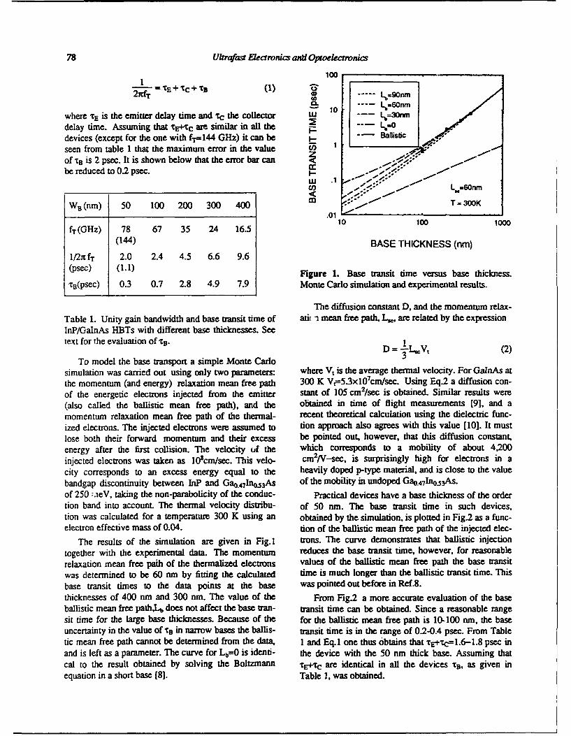
78 Ultrafost Ekerronics and Optoelectronics
100
CL 10 L-.60nrn
where "rE is the emitter delay time and Tc the collector U 10 Lb30nm
delay time. Assuming that t-Ecc are similar in all thedevices (except for the one with fr= 14 4 GHz) it can be i-- -- Banistic I.
seen from table I that the maximum error in the valueof "B is 2 psec. It is shown below that the error bar can <be reduced to 0.2 psec. -i
___ L,==6Onm
WB (nm) 50 100 200 300 400 - T = 300K
.0110 100 1000
fT (GHz) 78 67 35 24 16.5
(144) BASE THICKNESS (nm)
1/2n fT 2.0 2.4 4.5 6.6 9.6(psec) (1.1) Figure 1. Base transit time versus base thickness.
"cn(psec) 0.3 0.7 2.8 4.9 7.9 Monte Carlo simulation and experimental results.
The diffusion constant D, and the momentum relax-
Table 1. Unity gain bandwidth and base transit time of ati( 1 mean free path, L,,, are related by the expressionInP/GaInAs HBTs with different base thicknesses. Seetext for the evaluation of crl. 1
To model the base transport a simple Monte Carlo
simulation was carried out using only two parameters: where V, is the average thermal velocity. For GaInAs atthe momentum (and energy) relaxation mean free path 300 K Ve=5.3xl0 7cm/sec. Using Eq.2 a diffusion con-
of the energetic electrons injected from the emitter stant of 105 cm2/sec is obtained. Similar results were(also called the ballistic mean free path), and the obtained in time of flight measurements (9], and a
momentum relaxation mean free path of the thermal- recent theoretical calculation using the dielectric func-
ized electrons. The injected electrons were assumed to tion approach also agrees with this value [10]. It mustlose both their forward momentum and their excess be pointed out, however, that this diffusion constant,energy after the first collision. The velocity of the which corresponds to a mobility of about 4,200injected electrons was taken as 10'cm/sec. This velo- cm 2/V-sec, is surprisingly high for electrons in acity corresponds to an excess energy equal to the heavily doped p-type material, and is close to the valuebandgap discontinuity between InP and Ga0 .4 7h%.53As of the mobility in undoped Ga0.47In0.53As.
of 250 ;.aeV, taking the non-parabolicity of the conduc- Practical devices have a base thickness of the ordertion band into account. The thermal velocity distribu- of 50 run. The base transit time in such devices,tion was calculated for a temperature 300 K using an obtained by the simulation, is plotted in Fig.2 as a func-electron effective mass of 0.04. tion of the ballistic mean free path of the injected elec-
The results of the simulation are given in Fig.1 trons. The curve demonstrates that ballistic injection
together with the experimental data. The momentum reduces the base transit time, however, for reasonable
relaxation mean free paih of the thermalized electrons values of the ballistic mean free path the base transitwas determined to be 60 nm by fitting the calculated time is much longer than the ballistic transit time. This
base transit times to the data points at the base was pointed out before in Ref.8.
thicknesses of 400 nm and 300 nm. The value of the From Fig.2 a more accurate evaluation of the baseballistic mean free path.Lb does not affect the base tran- transit time can be obtained. Since a reasonable rangesit time for the large base thicknesses. Because of the for the ballistic mean free path is 10-100 rnm, the baseuncertainty in the value of CB in narrow bases the ballis- transit time is in the range of 0.2-0.4 psec. From Tabletic mean free path cannot be determined from the data, I and Eq.1 one thus obtains that rE+-C=1.6-1.8 psec inand is left as a parameter. The curve for Lb=O is identi- the device with the 50 nm thick base. Assuming thatcal to the result obtained by solving the Boltzmann rE-+rc are identical in all the devices 'cB, as given inequation in a short base (8]. Table 1, was obtained.
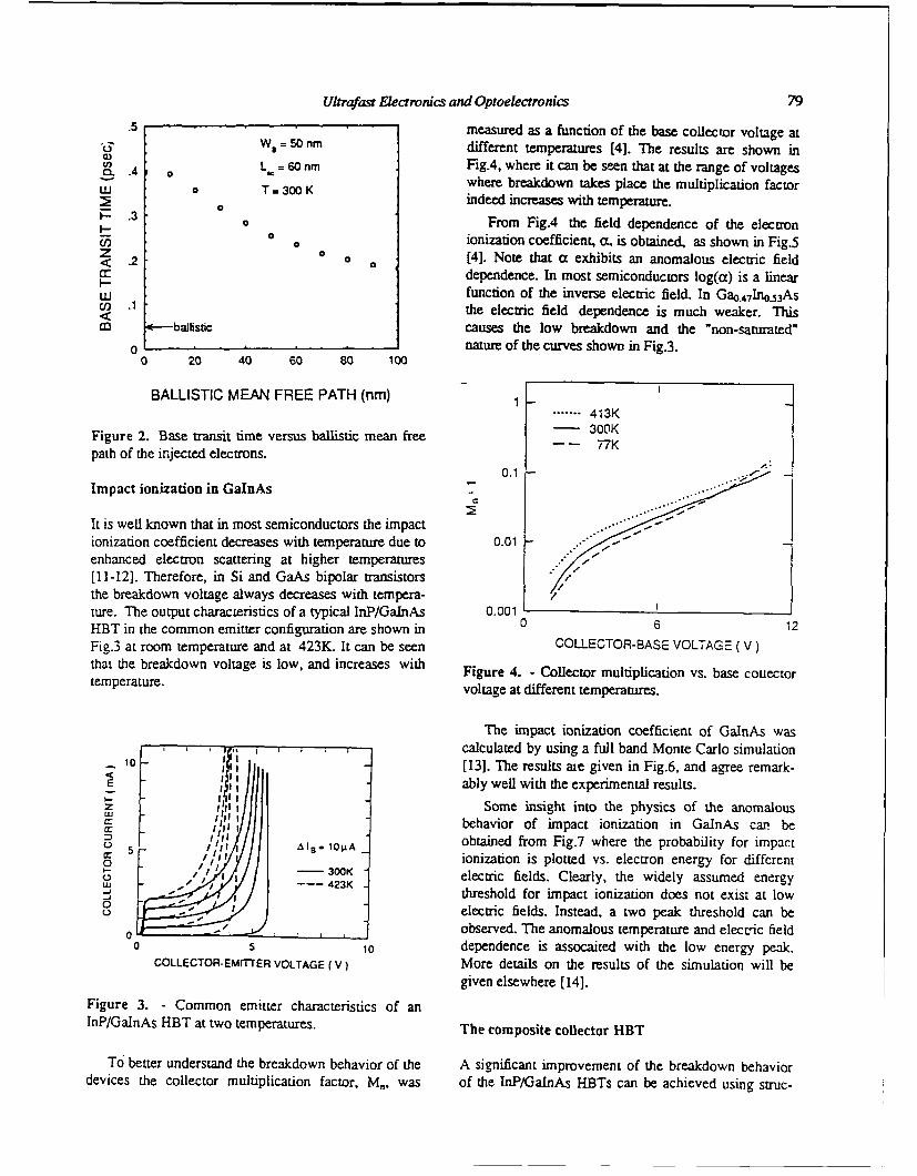
Ultrafast Electronics and Optoelectronics 79
.5 measured as a function of the base collector voltage atW= 50 am different temperatures [4]. The results are shown in
4 L =60nm Fig.4 , where it can be seen that at the range of voltages4 1where breakdown takes place the multiplication factorW 0 T=300 K0o indeed increases with temperature.
I--.3 From Fig.4 the field dependence of the electron0- oionization coefficient, a., is obtained, as shown in Fig.5
z ..2 [4]. Note that a exhibits an anomalous electric fieldq: dependence. In most semiconductors log(a) is a linear
.w function of the inverse electric field. In Gao.471no.53AsU) .1 the electric field dependence is much weaker. ThisM t-baflistic causes the low breakdown and the "non-saturated"
0 nature of the curves shown in Fig.3.0 20 40 60 80 100
BALLISTIC MEAN FREE PATH (nm) 1....... 413K
Figure 2. Base transit time versus ballistic mean free 300K
path of the injected electrons.0.1
Impact ionization in GaInAs
It is well known that in most semiconductors the impactionization coefficient decreases with temperature due to 0.01enhanced electron scattering at higher temperatures[11-12]. Therefore, in Si and GaAs bipolar transistorsthe breakdown voltage always decreases with tempera-ture. The output characteristics of a typical InP/GaInAs 0.001HBT in the common emitter configuration are shown in 0 6 12Fig.3 at room temperature and at 423K. It can be seen COLLECTOR-BASE VOLTAGE ( V)that the breakdown voltage is low, and increases with Figure 4. Collector multiplication vs. base colectortemperature. voltage at different temperatures.
The impact ionization coefficient of GalnAs was..... ; I .. calculated by using a full band Monte Carlo simulation
10 o [13]. The results aie given in Fig.6, and agree remark-It ably well with the experimental results.
z Some insight into the physics of the anomalousI'l behavior of impact ionization in GaInAs can. be
,,U;, obtained from Fig.7 where the probability for impact/i• ionization is plotted vs. electron energy for different
30K0o -electric fields. Clearly, the widely assumed energy73threshold for impact ionization does not exist at low
0electric fields. Instead, a two peak threshold can be0 , ,observed. The anomalous temperature and electric field0 s 10 dependence is assocaited with the low energy peak.
COLLECTOR-EMITTER VOLTAGE (V) More details on the results of the simulation will begiven elsewhere [14].
Figure 3. - Common emitter characteristics of anInP/GaInAs HBT at two temperatures. The composite collector HBT
To better understand the breakdown behavior of the A significant improvement of the breakdown behaviordevices the collector multiplication factor, M,, was of the InP/GaInAs HBTs can be achieved using struc-
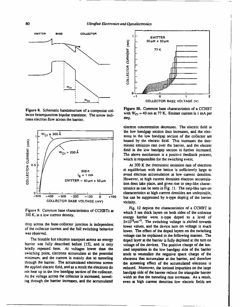
80 Ultrafast Electronics and Optoelectronics
EMrr'ER BASE COLLECTOR1EMITTER
50im x 50timE
77KLU
Cr.
0
LU-4"-J0
C.10 _
0 2Wc2 COLLECTOR BASE VOLTAGE (V)
Figure 8. Schematic bandstructure of a composite col- Figure 10. Common base characteristics of a CCHBTlector heterojunction bipolar transistor. The arrow indi- with Wct = 40 run at 77 K. Emitter current is 1 mA per
cares electron flow across the barrier. step-
electron concentration decreases. The electric field inthe low bandgap section thus increases, and the elec-
1- -, a 30Atrons in the low bandgap section of the collector areZ heated by the electric field. This increases the ther-E mionic emission rate over the barrier, and the electric
field in the low bandgap section is further increased.q: oThe above mechanism is a positive feedback process,
which is responsible for the switching event.
0.5 At 300 K the thermionic emission rate of electrons0- at equilibrium with the lattice is sufficiently large toS~300 KSIE = I mA avoid electron accumulation at low current densities.
However, at high current densities electron accumula-o EMITTER - 5O~m x50;&mo tion does take place, and gives rise to step-like charac-teristics as can be seen in Fig. 11. The step-like turn on
0 characteristics at high current densities are undesirable,-500 -400 -300 -200 -100 0 +100 but can be suppressed by n-type dopirg of the barrier
COLLECTOR BASE VOLTAGE (mV) vicinity
Figure 9. Common base characteristics of CCHBTs a Fig. 12 depicts the characteristics of a CCHBT inFig0r K, atoaowurnt densica rt is owhich 5 nn thick layers on both sides of the collector300 K, at a low current density. energy barrier were n-type doped to a level of
drop across the base-collector junction is independent 5xl012cm- 3. The switching voltage is shifted towardsdropf aross the acolletor currentjandthefun n sitcingbep t lower values, and the device turn on voltage is muchof the collector current and the full switching behavior lower. The effect of the doped layers on the switching
voltage can be explained in the following manner. TheThe bistable hot electron transport across an energy doped layer at the barrier is fully depleted at the turn on
barrier was fully described before (15], and is only voltage of the devices. The positive charge of the ion-briefly repeated here. At voltages lower than the ized impurities in the low bandgap side of the barrierswitching point, electrons accumulate at the potential tends to neutralize the negative space charge of theminimum, and the current is mainly due to tunneling electrons that accumulate at the barrier, and thereforethrough the barrier. The accumulated electrons screen the screening effect of the accumulated electrons isthe applied electric field, and as a result the electrons do reduced. Moreover, the ionized impurities on the largenot heat up in the low bandgap section of the collector. bandgap side of the barrier reduce the triangular barrierAs the voltage across the collector is increased, tunnel- width so that the tunneling rate increases. As a result,ing through the barrier increases, and the accumulated even at high current densities low electric fields are
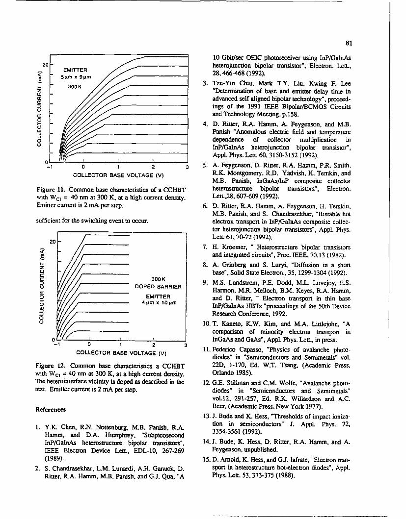
81
10 Gbit/sec OEIC photoreceiver using InP/GaInAs20 heterojunction bipolar transistor", Electron. Lett.,
2 E28,466-468 (1992).E• 5;.ro x 91Lm
ý:.- " 300 K /3. Tzu-Yin Chiu, Mark T.Y. Liu, Kwing F. Lee
zi "Determination of base and emitter delay time incc" advanced self aligned bipolar technology", proceed-
-- gs of the 1991 IEEE Bipolar/BCMOS Circuitsand Technology Meeting, p.158.
04. D. Ritter, RA. Hamm, A. Feygenson, and M.B.
w_ Panish "Anomalous electric field and temperature_J0 dependence of collector multiplication inoL InP/GaInAs heterojunction bipolar transistor",
Appl. Phys. LetL 60, 3150-3152 (1992).0-1 0 1 2 3 5. A. Feygenson, D. Ritter, R.A. Harem, P.R. Smith,
COLLECTOR BASE VOLTAGE (V) R.K. Montgomery, R.D. Yadvish, H. Temkin, andM.B. Panish, InGaAs/lnP composite collector
Figure 11. Common base characteristics of a CCHBT heterostructure bipolar transistors", Electron.with Wci = 40 nm at 300 K, at a high current density. Let.,28, 607-609 (1992).Emitter current is 2 mA per step. 6. D. Ritter, R.A. Harem, A. Feygenson, H. Temkin,
M.B. Panish, and S. Chandrasekhar, "Bistable hotsufficient for the switching event to occur. electron transport in InP/GaInAs composite collec-
tor heterojunction bipolar transistors", Appl. Phys.LetL 61, 70-72 (1992).20
Z 7. H. Kroemer, " Heterostructure bipolar transistorsE and integrated circuits", Proc. IEEE, 70,13 (1982).
Z_ 8. A. Grinberg and S. Luryi, "Diffusion in a shortx base", Solid State Electron., 35, 1299-1304 (1992).
300K 9. M.S. Lundstrom, P.E. Dodd, M.L. Lovejoy, E.S.o DOPED BARRIER Harmon, M.R. Melloch, B.M. Keyes, R.A. Hanem,
0 EMITTER and D. Ritter, " Electron transport in thin base4 urn x 10 urn InP/GaInAs HBTs "proceedings of the 50th Device
Research Conference, 1992.0
10. T. Kaneto, K.W. Kim, and M.A. Littlejohn, "Acomparison of minority electron transport in
0 2 InGaAs and GaAs", Appl. Phys. Lett., in press.- OLE21 2 11. Federico Capasso, "Physics of avalanche photo-COLLECTOR BASE VOLTAGE (V) diodes" in "Semiconductors and Semimetals" vol.
Figure 12. Common base characteristics a CCHBT 22D, 1-170, Ed. W.T. Tsang, (Academic Press,with Wc, = 40 nm at 300 K, at a high current density. Orlando 1985).The heterointerface vicinity is doped as described in the 12. G.E. Stillman and C.M. Wolfe, "Avalanche photo-text Emitter current is 2 mA per step. diodes" in "Semiconductors and Semimetals"
vol.12, 291-257, Ed. R.K. Willardson and A.C.
References Beer, (Academic Press, New York 1977).13. J. Bude and K. Hess, "Thresholds of impact ioniza-
1. Y.K. Chen, R.N. Nottenburg, M.B. Panish, R.A. tion in semiconductors" J. Appl. Phys. 72,
Hamre, and D.A. Humphrey, "Subpicosecond 3354-3561 (1992).
InP/GaInAs heterostructure bipolar transistors", 14. J. Bude, K. Hess, D. Ritter, R.A. Harmm, and A.IEEE Electron Device LetL, EDL-10, 267-269 Feygenson, unpublished.(1989). 15. D. Arnold, K. Hess, and GJ. Iafrate, "Electron tran-
2. S. Chandrasekhar, L.M. Lunardi, A.H. Ganuck, D. sport in heterostructure hot-electron diodes", Appl.Ritter, R.A. Hamnm, M.B. Panish, and GJ. Qua, "A Phys. Lett. 53, 373-375 (1988).
InP High Electron Mobility Transistors: Status and Promise
Loi D. Nguyen
Hughes Research Laboratories, 3011 Malibu Canyon Roa4 Malibu, California 90265
I. INTRODUCTION II. PRESENT STATUS OF InP HEMTs
The InP HEMT technology, once an exotic The InP HEMT presently exhibits the lowest noisetechnology in a few research laboratories, has begun to figures among all 3-terminal semiconductor devices. Forgain acceptance in the microwave and millimeterwave example, using 0.10 to 0.15-1am gatelength technology,community. Comparing to GaAs transistors, InP workers at Hughes and GE have independently reported aHEMTs exhibit significantly lower noise figures, noise figure below 1.0 dB at 60 GHz for InP HEMTs,higher gain, and higher cutoff frequencies [1], [2]. As aresult, they are now the most promising candidate for which is approximately 0.5 dB lower than the bestultralow-noise, ultrahigh-frequency, and ultrabroad-band reported results for GaAs HEMTs [1), [2).
amplifiers. The InP HEMT is also the first 3-terminal
In order to improve the performance of InP HEMTs semiconductor device which has demonstrated useful
further, significant efforts have been devoted to improve gain above 100 GHz. Recently, workers at TRW
the electron transport properties [31, [4], reduce the reported a successful demonstration of a 7.3 dB
parasitic resistances and gatelength [5], [6], and develop amplifier at 140 GHz using a 0.1 gtm gatelength InPa scaling model for sub-100 nanometer (nm) gatelength HEMT [9]. Assuming a simple 6 dB roll off, this
HEMTs [7]. Together, these efforts have led to a result indicates a power-gain cutoff frequency (fmax) of
successful fabrication of a 50-nm gatelength InP HEMT 325 GHz.with a state-of-the-art (extrinsic) transconductance (gm) In the last few years, the InP HEMT has also gained
of 1740 mS/mm and a state-of-the-art (extrinsic) more acceptance in the microwave and millimeterwavecurrent-gain cutoff frequency (fT) of 340 GHz [8] -- the community. At Hughes, for example, we are now
latter figure-of-merit corresponds to a total delay of only manufacturing 0.1 jtm gatelength InP HEMTs for low-
0.47 ps and represents a 70% improvement over typical noise applications covering the frequency range from 10fjT values of comparable 0.1 -ptm gatelength devices, to 94 GHz. Our present Pilot Line has been in
The 50-nm gatelength InP HEMT is currently the operation for approximately two years and is producing
most promising device to extend the operating frequency devices with a typical noise figure between 1.2 and 1.4
of 3-terminal semiconductor devices to the entire dB at 60 GHz.
millimeterwave spectrum, as well as to provide a low- As the InP HEMT technology becomes more mature,
cost alternative to ultralow-noise masers and SIS mixers it begins to be viewed as a critical technology for highat cryogenic temperatures. performance Monolithic Microwave/Millimeterwave
The main body of this paper is divided into 3 Integrated Circuits (MMICs). Some recent examples are
sections: Section II reviews the present status of InP the demonstration of a 5 to 100 GHz MMIC distributedHEMTs; Section III describes recent advances in 50-nm amplifier with 5 dB gain [10], a 75 to 100 GHz MMIC
gatelength InP HEMT technology; and, lastly, Section cascode amplifier with 8.0 dB gain [11 ], and a 12 GHz
IV discusses the potential of 50-nm gatelength InP MMIC low-noise amplifier with 0.8 dB noise figure
HEMTs for ultrahigh-frequency and ultralow-noise [12], all realized with InP HEMT technology.
receivers.
OSA Procea*nf on Uktrt,'. 0-Lauu," -,zd Opt~iecrromc 19,93. Vol. 14 82JagSdeep Sh md Umcgh mima (edi.0 1993 OpWc ai od'ttAmerica
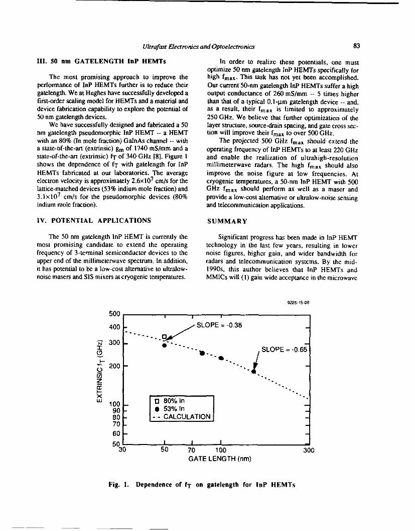
Ultrafast Electronics and Optoelectronics 83
III. 50 nm GATELENGTH InP HEMTs In order to realize these potentials, one mustoptimize 50 nm gatelength InP HEMTs specifically for
The most promising approach to improve the high fmax. This task has not yet been accomplished.performance of InP HEMTs further is to reduce their Our current 50-nm gatelength InP HEMTs suffer a highgatelength. We at Hughes have successfully developed a output conductance of 260 mS/mm -- 5 times higherfirst-order scaling model for HEMTs and a material and than that of a typical 0.1-1gm gatelength device -- and,device fabrication capability to explore the potential of as a result, their fmax is limited to approximately5o nm gatelength devices. 250 GHz. We believe that further optimization of the
We have successfully designed and fabricated a 50 layer structure, source-drain spacing, and gate cross sec-nm gatelength pseudomorphic InP HEMT -- a HEMT tion will improve their fmax to over 500 GHz.with an 80% (In mole fraction) GaInAs channel -- with The projected 500 GHz fmax should extend thea state-of-the-art (extrinsic) gm of 1740 mS/mm and a operating frequency of InP HEMTs to at least 220 GHzstate-of-the-art (extrinsic) fT of 340 GHz [8]. Figure 1 and enable the realization of ultrahigh-resolutionshows the dependence of fT with gatelength for InP millimeterwave radars. The high fmax should alsoHEMTs fabricated at our laboratories. The average improve the noise figure at low frequencies. Atelectron velocity is approximately 2.6x10 7 cm/s for the cryogenic temperatures, a 50-nm InP HEMT with 500lattice-matched devices (53% indium mole fraction) and GHz fmax should perform as well as a maser and3.xd10 7 cm/s for the pseudomorphic devices (80% provide a low-cost alternative or ultralow-noise sensingindium mole fraction). and telecommunication applications.
IV. POTENTIAL APPLICATIONS SUMMARY
The 50 nm gatelength lnP HEMT is currently the Significant progress has been made in InP HEMTmost promising candidate to extend the operating technology in the last few years, resulting in lowerfrequency of 3-terminal semiconductor devices to the noise figures, higher gain, and wider bandwidth forupper end of the millimeterwave spectrum. In addition, radars and telecommunication systems. By the mid-it has potential to be a low-cost alternative to ultralow- 1990s, this author believes that InP HEMTs andnoise masers and SIS mixers at cryogenic temperatures. MMICs will (1) gain wide acceptance in the microwave
9225-15-08
5005 0I I i
400 SLOPE -0.38
I 300--O "° .. -SLOPE =-0.65
F-_ 200
Z
X "Iu 100 13 80% In
901 53% In
80 - CALCULATION70O
60
50 I 1 -
30 50 70 100 300GATE LENGTH (nm)
Fig. 1. Dependence of fT on gatelength for lnP HEMTs
84
and millimeterwave community, (2) enable the 4. Chin et al., J. Vac. Sci. Technol., vol. B8, no. 2,realization of ultrahigh-resolution millimeterwave Mar./Apr. 1990.radars, and (3) provide a low-cost alternative to masers 5. Mishra et al., IEDM Tech. Dig., Dec. 1989.at cryogenic temperatures. 6. Nguyen et al., IEDM Tech. Dig., Dec. 1990.
7. Nguyen et al., IEEE Proceedings of the IEEE, vol.80, no. 4, Apr. 1992.
REFERENCES 8. Nguyen et al., IEEE Trans. Electron Devices, vol.39, no. 9, Sep. 1992.
1. Mishra et al., IEDM Tech. Dig., Dec. 1988. 9. Tan et al., IEDM Tech. Dig., Dec. 1991.2. Duh et al., IEEE Microwave and Guided Wave 10. Majidi-Ahy et al., Microwave Millimeter-Wave
Lett., vol. 1, no. 5, 1991. Monolithic Circuits Sym., 1990.3. Hong et al., J. Appl. Phys., vol. 64, no. 4, Aug. 11. Majidi-Ahy et al., GaAs IC Sym., 1990.
15, 1988. 12. Rosenbaum et al., IEEE MTT-S Dig., 1991.
High Speed Heterojunction JFETs Grown byNon-Hydride MOCVD
M. M. Hashemi, J. B. Shealy, S. P. DenBaars, and U. K. Mishra
Electrical and Computer Engineering Department and Materials Department,University of California, Santa Barbara, California 93106
Abstract communication systems despite the lack of a
Indium Phosphide channel JFET's with mature InP device technology, especially in
InGaAs lattice matched gate have been electronic devices. Indium Phosphide with
fabricated using liquid, non-hydride column high peak electron drift velocity , and large
V precursors. The incorporation of low intervalley separation (F-L = 0.63 eV, F-X
bandgap InGaAs gate layer not only = 0.73 eV) is a desirable material for high
suppresses hole injection under forward bias speed devices. In spite of excellent material
but also makes fabrication of HJFETs very properties, fabrication of high speed, high
reproducible and easy. Self-aligned devices performance FETs with InP channel has been
made by selective etching of the gate resulted a challenge in the past. Immature processing
in devices with current gain cut-off frequency technology along with low Schottky barrier
as high as 22 GHz with transconductance height ( OB < 0.5 eV for n-InP) and the high
over 200 mS/mm for gate length of about interface density of states between insulators
0.65 pgm. and InP makes fabrication of MESFET
impractical and MISFETs an unstable
Inrdt ion technology. Therefore, the JFET is aThere has been much interest in the reasonable compromise for a electronic
integration of optical devices along with device in InP system.
electronic devices to develop opto-electronic Heterojunction gate FETs were first
integrated circuits (OEIC's) which are implemented in GaAs channel device using p-
projected to have advantages of higher speed, AIGaAs material as the gate by Umebachi
smaller size, and higher reliability compared et.al. [1]. More complete characterization of
with discrete devices. The InP system is the a n-GaAs/P-A1GaAs HFET was reported by
only candidate for long-wavelength optical Morkoc et.al [2] with power gain cut-off
OSA Poceafip on hriqa ELecirrWcs and Optoe•croi 1993, VoL 14 85Jadeep SdS ad Un MiAn (ed*)0 1993 Oodcal Socialy 61AueNIM
86 Ultrafast Electronics and Optoelectronics
frequency (fmax) around 7-8 GHz. Recently new less toxic liquid alkyl column V sources
the same idea was applied to InGaAs channel replacing the extremely toxic and hazardous
HJFET using p-InP [31 or p-GaAs [4] as the hydrides (phosphine, arsine) [7,8]. Epitaxial
gate material. In all the previously reported growth starts with a 5000 A thick semi-
HFETs the gate material has been selected to insulating InP:Fe buffer layer. Next, a 2500
be of larger bandgap material primarily to A thick n-channel layer doped at 2-3X10¹⁷
enhance the built-in potential necessary to cm- 3 with electron mobility of =3000
improve the noise margin of the digital cm 2/V.s is grown fc!lowed by a 125 A thick
circuits.. However, hole injection from gate undoped lattice matched InxGaixA s
to the channel under forward bias condition, (x=0.53) spacer to account for diffusion of
which substantially limits the switching and zinc during subsequent growth of the p+
high frequency characteristics of JFETs, has layer. Finally, a 2500 A thick lattice matched
not been addressed in previously reported p-type InxGaIxAs (x=0.53) layer doped in
HJFETs. Recently [5,61, we have reported a excess of 1019 cn-- 3 was grown. Epitaxial
novel p+-InGaAs/n-Inp heterojunction cross section and energy band diagram is
combination as the gate and channel layer, shown in figure 1.
respectively to increase the high frequency Device processing starts with gate
performance of the HJFETs. This metallization (Ta/Au 200A/2800A) and lift-
combination is the first reported HJFET off to define a 1 g.m long gate. The gate
using InP as the channel. The p+-lnGaAs metal was used as the mask for etching the
gate layer offers several advantages over the InGaAs p+-layer. This was achieved using a
p-lnP layer used in the conventional selective wet chemical etch with controllable
homojunction JFETs: i) large valence band undercut resulting in a "T-shaped" gate
discontinuity for hole injection suppression ( structure. The gate length of the devices
AEv=0.37 eV), lower gate resistance (both measured in this study were about 0.6 g.m.
bulk and contact resistances), and ii) ease of Next the source-drain contacts (AuGefNiIAu
self-aligned fabrication using selective 1500A/150A/2000A) are formed by lift-off
etching of the gate layer. either in a self-aligned or non self-aligned
fashion. Finally, the devices were isolated
Device Fabrication and annealed. During the isolation step the
The HJFET structure was grown by non- gate pad is isolated from the source region by
hydride MOCVD at atmospheric pressure and forming an air bridge under the feed metal
at a substrate temperature of 560 'C using connecting gate pad to gate metal. This
tertiarybutylphosphine (TBP), and eliminates parasitic gate capacitance and gate
tertiarybutylarsine (TBA) as the alternative leakage important for high frequency
source for phosphine and arsine, operation of HJFETs. Figure 2 shows the
respectively. TBP and TBA are relatively SEM micrograph and corresponding cross
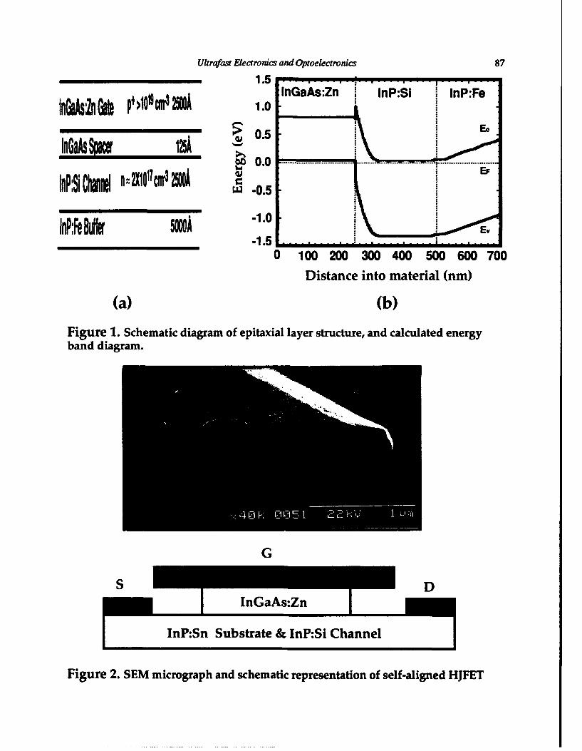
Ultrafast Electronics and Optoelectronics 871.5
InGaAs:Zn I inP:SI InP:FeInGaAs•n P+>1019c 21k 1.0
InGaAsSiW 125 0.0
w 0.5InP:Si Chianl n=21(1017cnr 21kA• o5
-1.00 100 200 300 400 500 600 700
Distance into material (nm)
(a) (b)
Figure 1. Schematic diagram of epitaxial layer structure, and calculated energyband diagram.
G
S DInGaAs:Zn
InP:Sn Substrate & InP:Si Channel
Figure 2. SEM micrograph and schematic representation of self-aligned HJFET
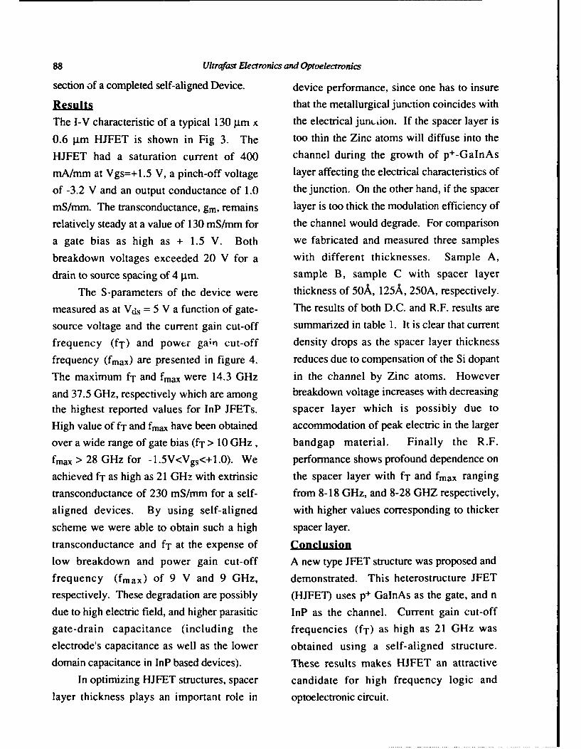
88 Ultrafast Electronics and Optoelectronics
section of a completed self-aligned Device. device performance, since one has to insure
Results that the metallurgical junction coincides with
The I-V characteristic of a typical 130 gim x the electrical junt.don. If the spacer layer is
0.6 g.m HJFET is shown in Fig 3. The too thin the Zinc atoms will diffuse into the
HJFET had a saturation current of 400 channel during the growth of p+-GaInAs
mA/mm at Vgs=+1.5 V, a pinch-off voltage layer affecting the electrical characteristics of
of -3.2 V and an output conductance of 1.0 the junction. On the other hand, if the spacer
mS/mm. The transconductance, gm, remains layer is too thick the modulation efficiency of
relatively steady at a value of 130 mS/mm for the channel would degrade. For comparison
a gate bias as high as + 1.5 V. Both we fabricated and measured three samples
breakdown voltages exceeded 20 V for a with different thicknesses. Sample A,
drain to source spacing of 4 jtm. sample B, sample C with spacer layer
The S-parameters of the device were thickness of 50A, 125A, 250A, respectively.
measured as at Vds = 5 V a function of gate- The results of both D.C. and R.F. results are
source voltage and the current gain cut-off summarized in table 1. It is clear that current
frequency (fT) and power gain cut-off density drops as the spacer layer thickness
frequency (fmax) are presented in figure 4. reduces due to compensation of the Si dopant
The maximum fT and fmax were 14.3 GHz in the channel by Zinc atoms. However
and 37.5 GHz, respectively which are among breakdown voltage increases with decreasing
the highest reported values for InP JFETs. spacer layer which is possibly due to
High value of fT and fmax have been obtained accommodation of peak electric in the larger
over a wide range of gate bias (fT > 10 GHz, bandgap material. Finally the R.F.
fmax > 28 GHz for -1.5V<Vgs<+1.0). We performance shows profound dependence on
achieved fT as high as 21 GHz with extrinsic the spacer layer with fT and fmax ranging
transconductance of 230 mS/mm for a self- from 8-18 GHz, and 8-28 GHZ respectively,
aligned devices. By using self-aligned with higher values corresponding to thicker
scheme we were able to obtain such a high spacer layer.
transconductance and fT at the expense of Conclusion
low breakdown and power gain cut-off A new type JFET structure was proposed and
frequency (fmax) of 9 V and 9 GHz, demonstrated. This heterostructure JFETrespectively. These degradation are possibly (HJFET) uses p÷ GaInAs as the gate, and n
due to high electric field, and higher parasitic InP as the channel. Current gain cut-off
gate-drain capacitance (including the frequencies (fT) as high as 21 GHz was
electrode's capacitance as well as the lower obtained using a self-aligned structure.
domain capacitance in InP based devices). These results makes HJFET an attractive
In optimizing HJFET structures, spacer candidate for high frequency logic and
layer thickness plays an important role in optoelectronic circuit.
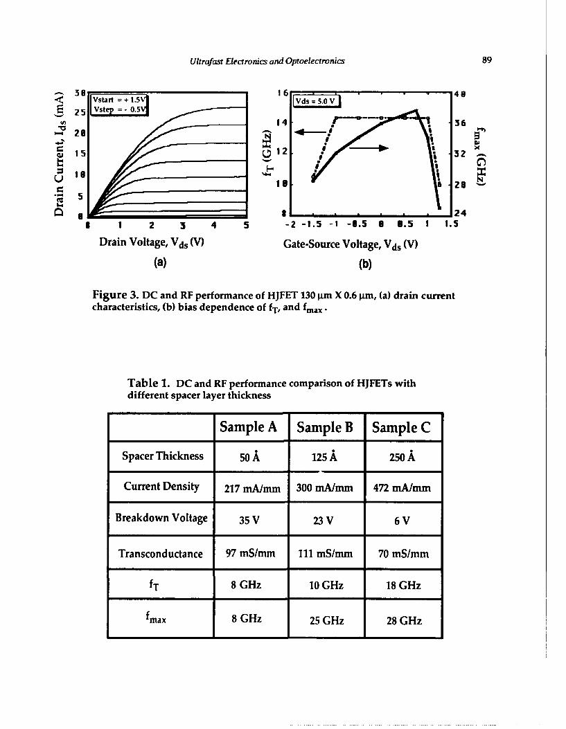
Ultrafast Electronics and Optoelectronics 89
38 16 48
- 28
w15 12 32
isi.E 5i o -- . 1 I•2 4
I 2 3 4 5 -2 -1.5 -1 -8.5 8 8.5 1 1.5
Drain Voltage, Vds (V) Gate-Source Voltage, Vds (V)
(a) (b)
Figure 3. DC and RF performance of HJFET 130 gm X 0.6 pum, (a) drain currentcharacteristics, (b) bias dependence of fT, and fmax-
Table 1. DC and RF performance comparison of HJFETs withdifferent spacer layer thickness
Sample A Sample B Sample C
Spacer Thickness so A 125 A 250 A
Current Density 217 mA/mm 300 mA/mm 472 mA/mm
Breakdown Voltage 35 V 23 V 6 V
Transconductance 97 mS/mm 111 mS/mm 70 mS/mm
fT 8 GHz 10 GHz 18 GHz
fmax 8 GHz 25 GHz 28 GHz
90
References DenBaars, and U.K. Mishra, IEDM Tech.
[1) S. Umebachi, K. Asahi, M. Inoue, and Dig., 311, 1993.
G. Kano, IEEE Trans. Elec. Dev. ED-22, [61 M.M. Hashemi, J.B. Shealy, S.P.
613, 1975. DenBaars, and U.K. Mishra, To be
121 H. Morkoc, S.G. Bandy, R. Sankaran, published in IEEE Elec. Dev. Lett., Feb.,
G.A. Antypas, and R.L. Bell, IEEE Trans. 1993.
Elec. Dev. ED-25, 619, 1978. 171 C.A. Larsen, N.I. Buchan, S.H. Li, and
[3] D. Wake, A.W. Nelson, S.Cole, S. G.B. Stringfellow, J. Cryst. Growth,
Wong, I.D. Henning, and E.G. Scott, IEEE Vol.93, 15, 1988.
Elec. Dev. Lett. EDL-6, 626, 1985. [8] C.H. Chen, C.A. Larsen, G.B.
[41 C.L. Lin, H.H. Wieder, R. Zuleeg, IEEE Stringfellow, D.W. Brown, and A.J.
Elec. Dev. Lett. EDL- 11, 30, 1990. Robertson, J. Cryst. Growth, Vol.77, 11,
[51 M.M. Hashemi, J.B. Shealy, S.P. 1986.
Resonant-Tunneling Transmission-LineRelaxation Oscillator
E. R. Brown
Lincoln Laboratory, Massachusetts Institute of Technology,Lexington; Massachusetts 02173-9108
Abstract makes it very difficult to achieve dc bias stability inthis region. Consequently, only small-area diodes
A new type of resonant-tunneling oscillator is having a suitably high differential resistance can beanalyzed that does not require dc bias stability in the used. In the case of oscillators, the small area leadsnegative-differential-resistance region. The oscillator to a low output power relative to other two-terminalconsists of a resonant-tunneling diode coupled to a negative-resistance devices, such as Gunn andtransmission line in such a way that repetitive IMPATT" diodes. To overcome this shortcoming, oneswitching of the diode occurs across the negative- must design either an RTD oscillator that does notresistance region. The output waveform consists of a require dc stability in the NDR region or a new typesequence of pulses having a repetition rate deter- of RTD that provides a wider NDR region for grea.ermined by the electrical delay of the transmission line ease of dc biasing in large-area diodes. The presentand a pulse width determined by the switching time oscillator approach makes it possible to bias the RTDof the diode. When the electrical delay is compar- in a positive-differential-resistance (PDR) region soable to the switching time, the output is quasi- that dc bias stability can be easily achieved.sinusoidal. Numerical simulations with a prototyperesonant-tunneling diode yield a maximum repetition Relaxation Oscillatorrate of 192 GHz and a pulse width of 2 ps.
The new RTD oscillator is based on the repetitiveswitching through the NDR region between dc-stable
Introduction points lying below the peak point and above the val-ley point. To establish this type of oscillation, we
The resonant-tunneling diode (RTD) has been one of imagine that the RTD is connected to one end of athe most successful quantum-transport devices. The short-circuited transmission line, as shown in Fig. 1.trademark characteristic of the RTD, the negative- The transmission line has a characteristic impedancedifferential-resistance (NDR) region, has been Z0 and an electrical time delay td. The RTD isobserved at room temperature in many different biased through a bias resistor RL with a supply vol-material systems and over a very wide range of tage VB. The quiescent operation point is initiallycurrent density. The NDR region has been used as just below the peak or just above the valley, and thethe basis for high-frequency oscillations and high- RTD is induced to switch toward the valley or peak,speed switcning. For example, double-barrier RTDs respectively, by a slowly applied voltage ramp AV.made from the InAs/AlSb system have oscillated up Once the first switch occurs, a pulse travels down theto 712 GHz [11, and similar diodes made from the line, is reflected from the short with inverted polarity,GaAs/AIAs system have switched from the peak and arrives back at the RTD after a time 2td. If 2tdpoint to the valley region in a time near 2 ps 12]. is sufficiently greater than the RTD switching time t1,Much of the interest in RTDs stems from the fact then the return pulse will induce the RTD to switchthat these results are among the highest oscillation back to the initial operating point. The subsequentfrequencies and the lowest switching times reported return pulse then induces a switch similar to the firstto date for electronic devices, one, and the process repeats at a rate of (4td)-l. The
In spite of these successes, the double-barrier overall process is classified as a relaxation oscillationRTD has one fundamental shortcoming for the oscil- because the RTD dwells in either of its PDR regionslator application. The steep slope in the NDR region between switching events.
OSA Proceedings on Ukrafast Electronics and Optoekectronics 1993, VoL 14 91Jagdeep Shah and Umesh Mishra (ed!.)0 1993 Optical Socktey ofAmerica
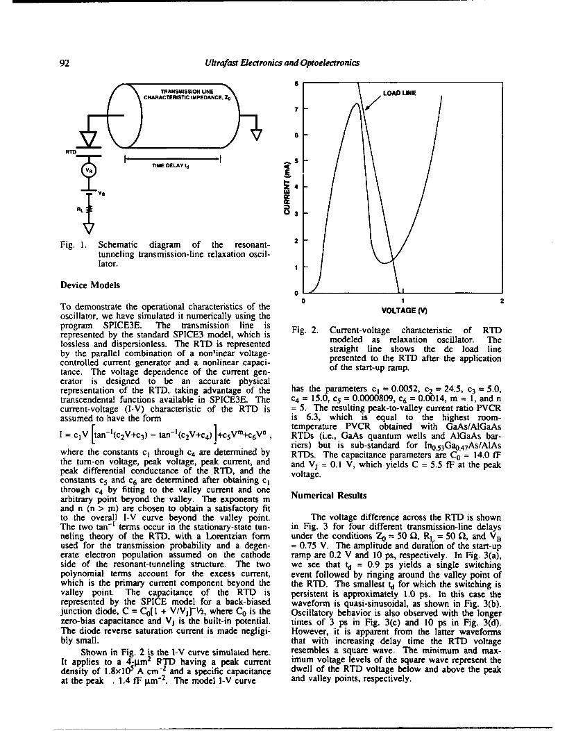
92 Ultrafast Electronics and Optoelectronics
TRANSSS 0LINELOAD LINE
TIME DELAY td
RL '3
Fig. 1. Schematic diagram of the resonant- 2tunneling transmission-line relaxation oscil-lator.1
Device Models0
0 12To demonstrate the operational characteristics of the VLAE(/oscillator, we have simulated it numerically using theVOTG()program SPICE3E. The transmission line is Fi.2 Curn-otg chatesic fRTrepresented by the standard SPICE3 model, which is Fi.2 Curn-otg chatesic fRTlossless and dispersionless. The RTD is represented smoaghtlied ashrl tows thesciloador lineby the parallel combination of a nonlinear voltage- prsetrih lned t ho w the dTcate theapplicaincontrolled current generator and a nonlinear capaci- peetdt h T fe h plctotance. The voltage dependence of the current gen- of the start-up ramp.erator is designed to be an accurate physicalrepresentation of the RTD, taking advantage of the has the parameters c1 0.0052, c2 = 24.5, c3 = 5.0,transcendenta! functions available in SPICE3E. The c4 = 15.0, c5 = 0.0000809, c6 = 0.0014, m = 1, and acurrent-voltage (I-V) characteristic of the RTD is = 5. The resulting, peak-to-valley current ratio PVCRassumed to have the form is 6.3, which is equal to the highest room-
1a temperature PVCR obtained with GaAs/AIGaAsIc=VctV -1(c2 V+c 3) -- tan-I(c2 V+c 4)I"1C5vm-1" 6 Vn, RTDs (i.e., GaAs quantum wells and AIGaAs bar-
- ~riers) but is sub-standard for In0 _53Gao.4 7As/AIAswhere the constants cI through c4 are determined by RTDs. The capacitance parameters are CO0 14.0 fFthe turn-on voltage, peak voltage, peak current, and and V1 = 0.1 V, which yields C = 5.5 fF at the peakpeak differential conductance of the RTD, and the voltage.constants c5 and c6 are determined after obtaining c1through c4 by fitting to the valley current and onearbitrary point beyond the valley. The exponents m NuecaRsltand n (n > m) are chosen to obtain a satisfactory fitto the overall I-V curve beyond the valley point. The voltage difference across the RTD is shownThe two tan-t terms occur in the stationary-state tun- in Fig. 3 for four different transmission-line delaysneling theory of the RTD, with a Lorentzian form under the conditions Z0 = 50 •, RL = 50 fl1, and VBused for the transmission probability and a degen- = 0.75 V. The amplitude and duration of the stant-upcrate electron population assumed on the cathode ramp are 0.2 V and 10 ps, respectively. In Fig. 3(a),side of the resonant-tunneling structure. The two we see that td = 0.9 ps yields a single switchingpolynomial terms account for the excess current, event followed by ringing around the valley point ofwhich is the primary current component beyond the the RTD. The smallest td for which the switching isvalley point. The capacitance of the RTD is persistent is approximately 1.0 ps. In this case therepresented by the SPICE model for a back-biased waveform is quasi-sinusoidal, as shown in Fig. 3(b).junction diode, C = Cot 1 + V/Vj]-1/2, where CO is the Oscillatory behavior is also observed with the longerzero-bias capacitance and V1 is the built-in potential. times of 3 ps in Fig. 3(c) and 10 ps in Fig. 3(d).The diode reverse saturation current is made negligi- However, it is apparent from the latter waveformsbly small. that with increasing delay time the RTD voltage
Shown in Fig. 2 is the I-V curve simulated here. resembles a square wave. The minimum and max-It applies to a 4-jim 2 IPTD having a peak current imum voltage levels of the square wave represent thedensity of 1.8xl1& A cm- and a specific capacitance dwell of the RTD voltage below and above the peakat the peak .1.4 IF •tm-2. The model I-V curve and valley points, respectively.
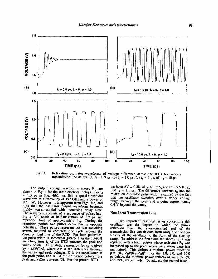
Ultrafast Electronics and Optoelectronics 93
1.5
> 1.0
I-.
0> 0.5
(a) td=0.9pS,L=O, p=1.0 (b) td 1.0 ps, L0, p 1.0
1.5
> 1.0
-J
0> 0.5
(C) td 3.0 ps, L O, p= 1.0 (d) td =10.0 psL0, p 1.0
0.00 20 40 60 s0 100 0 20 40 60 s0 100
TIME (ps) TIME (ps)
Fig. 3. Relaxation oscillator waveforms of voltage difference across the RTD for varioustransmission-line delays: (a) td = 0.9 ps, (b) td = 1.0 ps, (c) td = 3 ps, (d) td = 10 Ps.
we have AV = 0.28, Al = 6.0 mA, and C = 5.5 fF, soThe output voltage waveforms across RL are that tR = 1.1 ps. The difference between tR and the
shown in Fig. 4 for the same electrical delays. For td relaxation oscillator pulse width is caused by the fact= 1.0 ps in Fig. 4(b), we find a quasi-sinusoidal that the oscillator switches over a wider voltagewaveform at a frequency of 192 GHz and a power of0.5 mW. However, it is apparent from Figs. 4(c) and 0.4 V beyond the valley.4(d) that the oscillator output waveform becomeshighly non-sinusoidal with increasing delay time.The waveform consists of a sequence of pulses hay- Non-Ideal Transmission Lineing a full width at half-maximum of 1.9 ps andrepetition time of approximately 4 td. During the Two important practical issues concerning thisrepetition period two pulses occur having opposite oscillator are the degree to which the powerpolarities. These pulses represent the two switching reflection from the short-circuited end of theevents required to complete one cycle around the transmission line can deviate from unity and the sen-dynamic load line of the RTD. For both polarities, sitivity of the oscillator to the form of the start-upthe pulse width is somewhat greater than the 10-90% ramp. To address the first issue the short circuit wasswitching time tR of the RTD between the peak and replaced with a load resistor whose resistance RT wasvalley points. An analytic expression for tR is given increased up to the point where oscillations were justby 4.4AVC/AJ, where AV is the difference between maintained. This defines a minimal power reflectionthe valley and peak voltages, C is the capacitance at p = [(RT-Zo)/(R 14Z 0)Iz. For the 1.0, 3.0, and 10.0the peak point, and A I is the difference between the ps delays, the minimal power reflections were 97, 69,peak and valley currents [3]. For the present RTD and 59%, respectively. To address the second issue,
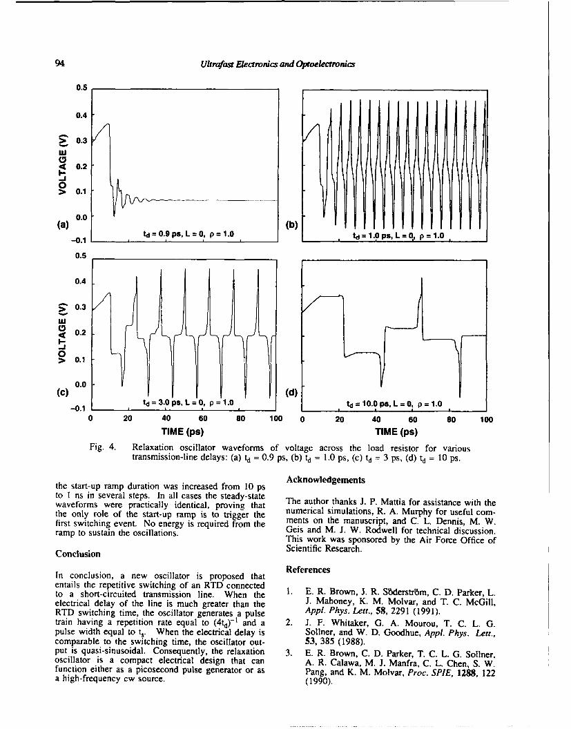
94 Ultrafast Electronics and Optoelectronics
0.5
0.4
> 0.3
4 0.2
0> 0.1
0.0(a) (b)-0.1 td=0.9ps, L=O, p=l.0 td 1.OpsL R, p 1.0
0.5
0.4
> 0.3
< 0.2-J0> 0.1
0.0(C) (d)
td = 3 .0 ps, L =O, p= 1.0 td =10.0 ps, L =0, p= 1.0-0.1 _ _ _ _ __ _ _
0 20 40 60 80 100 0 20 40 60 80 100TIME (ps) TIME (ps)
Fig. 4. Relaxation oscillator waveforms of voltage across the load resistor for varioustransmission-line delays: (a) td = 0.9 ps, (b) td = 1.0 ps, (c) td = 3 ps, (d) td = 10 Ps.
Acknowledgementsthe start-up ramp duration was increased from 10 psto I ns in several steps. In all cases the steady-state The author thanks J. P. Mattia for assistance with thewaveforms were practically identical, proving that The ra l t ions R. . M urphy for us e com-the only role of the start-up ramp is to trigger the numerical simulations, R. A. Murphy for useful com-first switching event. No energy is required from the ments on the manuscript, and C. L. Dennis, M. W.ramp to sustain the oscillations. Geis and M. J. W. Rodwell for technical discussion.
This work was sponsored by the Air Force Office ofConclusion Scientific Research.
ReferencesIn conclusion, a new oscillator is proposed thatentails the repetitive switching of an RTD connectedto a short-circuited transmission line. When the J. E. RhBrown, K. R. Slderstrlm, C. D. Parker, L.electrical delay of the line is much greater than the 3. Mahoney, K. M. Molvar, and T. C. McGill,RTD switching time, the oscillator generates a pulse Appl. Phys. Lett., 58, 2291 (1991).train having a repetition rate equal to (4td)-l and a 2. J. F. Whitaker, G. A. Mourou, T. C. L. G.pulse width equal to t,. When the electrical delay is Sollner, and W. D. Goodhue, Appl. Phys. Lett.,comparable to the switching time, the oscillator out- 53, 385 (1988).put is quasi-sinusoidal. Consequently, the relaxation 3. E. R. Brown, C. D. Parker, T. C. L. G. Sollner,oscillator is a compact electrical design that can A. R. Calawa, M. J. Manfra, C. L. Chen, S. W.function either as a picosecond pulse generator or as Pang, and K. M. Molvar, Proc. SPIE, 1288, 122a high-frequency cw source. (1990).
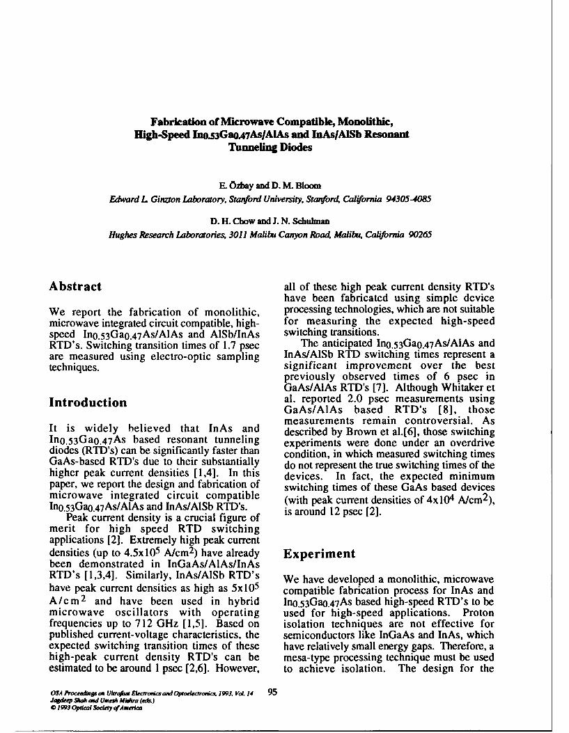
Fabrication of Microwave Compatible, Monolithic,High-Speed Ino_53Ga0A7AsIAIAs and InAs/AISb Resonant
Tunneling Diodes
E. Ozbay and D. M. Bloom
Edward L Ginzron Laboratory, Stanford University, Stanfor4 California 94305-4085
D. H. Chow and J. N. SchulmanHughes Research Laboratories, 3011 Malibu Canyon Roa4 Malibu, California 90265
Abstract all of these high peak current density RTD'shave been fabricated using simple device
We report the fabrication of monolithic, processing technologies, which are not suitablemicrowave integrated circuit compatible, high- for measuring the expected high-speedspeed In 0 .53Ga 0.47 As/AlAs and AISb/InAs switching transitions.RTD's. Switching transition times of 1.7 psec The anticipated InO.5 3GaO.47As/AlAs andare measured using electro-optic sampling InAs/AlSb RTD switching times represent atechniques. significant improvement over the best
previously observed times of 6 psec inGaAs/AlAs RTD's [7]. Although Whitaker et
Introduction al. reported 2.0 psec measurements usingGaAs/AlAs based RTD's [8], thosemeasurements remain controversial. As
It is widely believed that InAs and described by Brown et al.[6], those switchingInO.53GaO.4 7 As based resonant tunneling experiments were done under an overdrivediodes (RTD's) can be significantly faster than condition, in which measured switching timesGaAs-based RTD's due to their substantially do not represent the true switching times of thehigher peak current densities [1,41. In this devices. In fact, the expected minimumpaper, we report the design and fabrication of switching times of these GaAs based devicesmicrowave integrated circuit compatible (with peak current densities of 4x10 4 A/cm2 ),InO.53Ga0.47As/AlAs and InAs/AlSb RTD's. is around 12 psec [2].
Peak current density is a crucial figure ofmerit for high speed RTD switchingapplications [2]. Extremely high peak currentdensities (up to 4.5xl0 5 A/cm 2 ) have already Experimentbeen demonstrated in InGaAs/AlAs/InAsRTD's [1,3,4]. Similarly, InAs/AlSb RTD's We have developed a monolithic, microwavehave peak current densities as high as 5x10 5 compatible fabrication process for InAs andA/cm 2 and have been used in hybrid InO.5 3GaO.47As based high-speed RTD's to bemicrowave oscillators with operating used for high-speed applications. Protonfrequencies up to 712 GHz [1,5]. Based on isolation techniques are not effective forpublished current-voltage characteristics, the semiconductors like InGaAs and InAs, whichexpected switching transition times of these have relatively small energy gaps. Therefore, ahigh-peak current density RTD's can be mesa-type processing technique must be usedestimated to be around 1 psec [2,61. However, to achieve isolation. The design for the
OSA Proceedinp on Ultra4w Electrons and Optoelectrovnc 1993, Vol. 14 95Jqdeep Shah and UmeA Mashra (edw)0 1993OQpdilSocky cAnwdkn
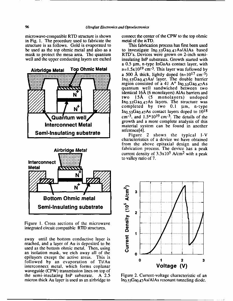
96 Ultrafast Electronics and Optoelectronics
microwave-compatible RTD structure is shown connect the center of the CPW to the top ohmicin Fig. 1. The procedure used to fabricate the metal of the RTD.structure is as follows. Gold is evaporated to This fabrication process has first been usedbe used as the top ohmic metal and also as a to investigate In0.53Ga0.47As/AlAs basedmask to protect the mesa area. The quantum RTD's. Devices were grown on 2-inch semi-well and the upper conducting layers are etched insulating InP substrates. Growth started with
a 0.5 gm, n-type InGaAs contact layer, withAirbrldge Metal Top Ohmic Metal n=1.5x 1019 cm-3. This layer was followed by
a 500 A thick, lightly doped (n=10 17 cm-3)Sn0.53Ga0.47As/ layer. The double barrier
region consisted of a 41 A' Ino.5 3Gao.4 7 As.quantum well sandwiched between two
identical 16A (6 monolayers) AlAs barriers andtwo 15A (5 monolayers) undopedln0.53Ga0.47As layers. The structure wascompleted by two 0.1 gm, n-typeIn0.53Ga0.47As contact layers doped to 1018
QOuantum well cm- 3 , and 1.5* 1019 cm- 3 . The details of thegrowth and a more complete analysis of this
Interconnect Metal material system can be found in anotherS sreference[4].Semi-Insulatingsubstrate Figure 2 shows the typical I-V
characteristics of a device we have obtainedfrom the above epitaxial design and the
Airbridge Metal fabrication process. The device has a peakcurrent density of 3.3x10⁵ A/cm2 with a peakto valley ratio of 7.
Interconnect
Metal
Bottom Ohmic metalLIM
Semi-Insulating substrate
Figure 1. Cross sections of the microwaveintegrated circuit compatible RTD structures. .1
away until the bottom conductive layer isreached, and a layer of Au is deposited to beused as the bottom ohmic metal. Then, usingan isolation mask, we etch away all of the 0 1epilayers except the active areas. This isfollowed by an evaporation of Ti/Au 0 1 2interconnect metal, which forms coplanar Voltage (V)waveguide (CPW) transmission lines on top ofthe semi-insulating InP substrate. A 2.5 Figure 2. Current-voltage characteristic of anmicron thick Au layer is used as an airbridge to ln0.53Ga0.47As/AIAs resonant tunneling diode.
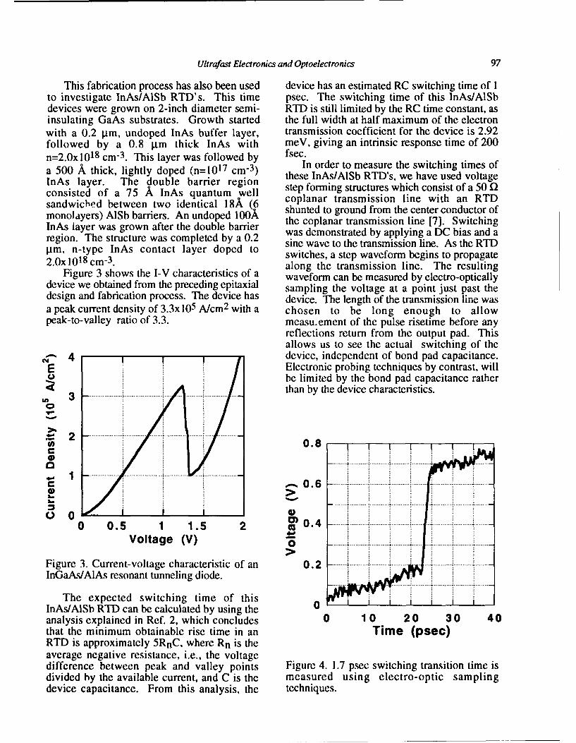
Ultrafast Electronics and Optoelectronics 97
This fabrication process has also been used device has an estimated RC switching time of 1to investigate InAs/AISb RTD's. This time psec. The switching time of this InAs/AlSbdevices were grown on 2-inch diameter semi- RTD is still limited by the RC time constant, asinsulating GaAs substrates. Growth started the full width at half maximum of the electronwith a 0.2 .tm, undoped InAs buffer layer, transmission coefficient for the device is 2.92followed by a 0.8 gtm thick InAs with meV, giving an intrinsic response time of 200n=2.0x 1018 cm-3 . This layer was followed by fsec.
0A thick, lightly doped (n=10 17 cm- 3) In order to measure the switching times of500 A layer. The dope barrier rm-i) these InAs/A1Sb RTD's, we have used voltageInAs layer. The double barrier region
consisted of a 75 A InAs quantum well step forming structures which consist of a 50 Q
sandwiched between two identical 18A (6 coplanar transmission line with an RTD
monolayers) A1Sb barriers. An undoped 100A shunted to ground from the center conductor of
InAs layer was grown after the double barrier the coplanar transmission line [7]. Switchingregion. The structure was completed by a 0.2 was demonstrated by applying a DC bias and aregion.The strucontueast competded by a. sine wave to the transmission line. As the RTDp.m. n-type InAs contact layer doped to switches, a step waveform begins to propagate2-0xl 018 cm-3. along the transmission line. The resulting
Figure 3 shows the I-V characteristics of a waveform can be measured by electro-opticallydevice we obtained from the preceding epitaxial sampling the voltage at a point just past thedesign and fabrication process. The device has device. The length of the transmission line wasa peak current density of 3.3xI05 A/cm 2 with a chosen to be long enough to allowpeak-to-valley ratio of 3.3. measu.ement of the pulse risetime before any
reflections return from the output pad. Thisallows us to see the actual switching of the
S4 device, independent of bond pad capacitance.E Electronic probing techniques by contrast, will0 be limited by the bond pad capacitance rather
than by the device characteristics.
00.• o .6 ...........................................
0 ~ ~ ~~ ..... ... ... 4.-.......................0 0.8115 [2o t g .V ....... ....... ... .. ...... .. .. .... .... ... .... .......
0).
F i u r .. ....... C u r r e n t - ... ta g e ...... r i ti .. ... .. ... 2.. .. .. . . .. . .. ... .... .. ... . .. . .. . .. ... . .. . .
0
The 1 xetdsicigtm fti0 0 .5 1 1 .5 2 ~ 0 .4 ..... ............ ......... ...............
Voltage (V)
Figure 3. Current-voltage characteristic of an 0.2 ................ ....InGaAs/AlAs resonant tunneling diode.
The expected switching time of this ________
InAs/AISb RTD can be calculated by using the 0analysis explained in Ref. 2, which concludes 0 1 0 20 30 40that the minimum obtainable rise time in an Time (psec)RTD is approximately 5RnC, where Rn is theaverage negative resistance, i.e., the voltagedifference between peak and valley points Figure 4. 1.7 psec switching transition time isdivided by the available current, and C is the measured using electro-optic samplingdevice capacitance. From this analysis, the techniques.
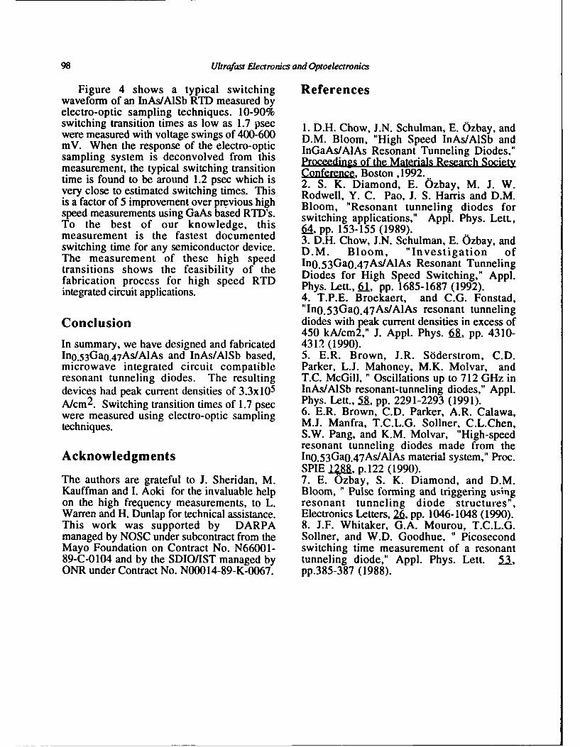
98 Ultrafost Electronics and Optoelectronics
Figure 4 shows a typical switching Referenceswaveform of an InAs/AlSb RTD measured byelectro-optic sampling techniques. 10-90%switching transition times as low as 1.7 psec 1. D.H. Chow, J.N. Schulman, E. Ozbay, andwere measured with voltage swings of 400-600 D.M. Bloom, "High Speed InAs/AlSb andmV. When the response of the electro-optic InGaAs/AlAs Resonant Tunneling Diodes,"sampling system is deconvolved from this Proceedings of the Materials Research Societymeasurement, the typical switching transition Conference, Boston 1992.time is found to be around 1.2 psec which is 2. S. K. Diamond, E. Ozbay, M. J. W.very close to estimated switching times. This Rodwell, Y. C. Pao, J. S. Harris and D.M.is a factor of 5 improvement over previous high Bloom, "Resonant tunneling diodes forspeed measurements using GaAs based RTD's. switching applications," Appl. Phys. Lett.,To the best of our knowledge, this 6A, pp. 153-155(1989).measurement is the fastest documented 3. D.H. Chow, J.N. Schulman, E. Ozbay, andswitching time for any semiconductor device. D. M. Bloom, "Investigation ofThe measurement of these high speed In0.53Ga0.47As/AlAs Resonant Tunnelingtransitions shows the feasibility of the Diodes for High Speed Switching," Appl.fabrication process for high speed RTD Phys. Lett., El, pp. 1685-1687 (1992).integrated circuit applications. 4. T.P.E. Broekaert, and C.G. Fonstad,
"InO.53Ga0.47As/AlAs resonant tunnelingConclusion diodes with peak current densities in excess of
450 kA/cm2," J. Appl. Phys. 68, pp. 4310-In summary, we have designed and fabricated 4312 (1990).In0.53Ga0.4 7As/AlAs and InAs/AlSb based, 5. E.R. Brown, J.R. Soderstrom, C.D.microwave integrated circuit compatible Parker, L.J. Mahoney, M.K. Molvar, andresonant tunneling diodes. The resulting T.C. McGill, " Oscillations up to 712 GHz indevices had peak current densities of 3.3x10 5 InAs/AlSb resonant-tunneling diodes," Appl.A/cm 2 . Switching transition times of 1.7 psec Phys. Lett., 5R, pp. 2291-2293 (1991).were measured using electro-optic sampling 6. E.R. Brown, C.D. Parker, A.R. Calawa,techniques. M.J. Manfra, T.C.L.G. Sollner, C.L.Chen,S.W. Pang, and K.M. Molvar, "High-speed
resonant tunneling diodes made from theAcknowledgments In0.53Ga0.47As/AlAs material system," Proc.
SPIE =.., p. 12 2 (1990).The authors are grateful to J. Sheridan, M. 7. E. Ozbay, S. K. Diamond, and D.M.Kauffman and I. Aoki for the invaluable help Bloom, " Pulse forming and triggering usingon the high frequency measurements, to L. resonant tunneling diode structures",Warren and H. Dunlap for technical assistance. Electronics Letters, 2.6, pp. 1046-1048 (1990).This work was supported by DARPA 8. J.F. Whitaker, G.A. Mourou, T.C.L.G.managed by NOSC under subcontract from the Sollner, and W.D. Goodhue, " PicosecondMayo Foundation on Contract No. N66001- switching time measurement of a resonant89-C-0104 and by the SDIO/IST managed by tunneling diode," Appl. Phys. Lett. 51,ONR under Contract No. N00014-89-K-0067. pp.385-387 (1988).

Terahertz Transients
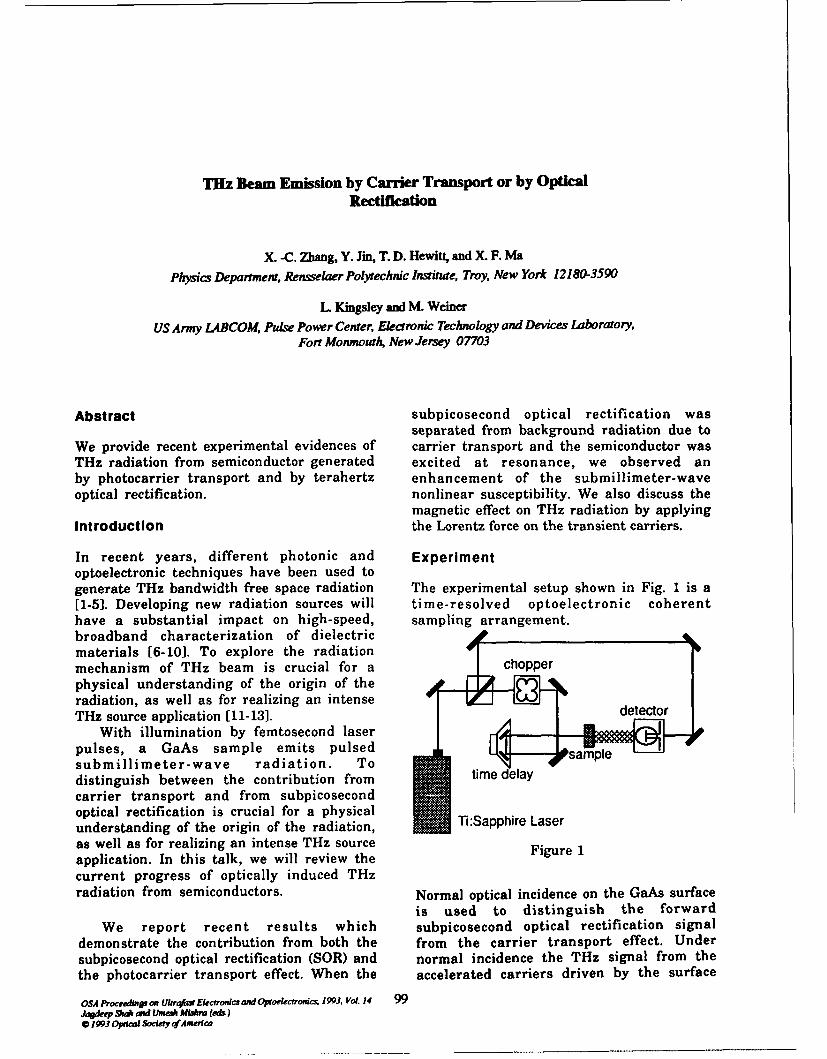
TRz Beam Emission by Carrier Transport or by OpticalRectification
X. -C. Zhamg, Y. Jin, T. D. Hewitt, and X. F. MaPhysics Department, Rensselaer Polytechnic Insliture, Troy, New York 12180-3590
L. Kingsley and M. Weiner
US Army LABCOM, Pulse Power Center, Electronic Technology and Devices Laboratory,Fort Monmouth, New Jersey 07703
Abstract subpicosecond optical rectification wasseparated from background radiation due to
We provide recent experimental evidences of carrier transport and the semiconductor wasTHz radiation from semiconductor generated excited at resonance, we observed anby photocarrier transport and by terahertz enhancement of the submillimeter-waveoptical rectification. nonlinear susceptibility. We also discuss the
magnetic effect on THz radiation by applying
Introduction the Lorentz force on the transient carriers.
In recent years, different photonic and Experimentoptoelectronic techniques have been used togenerate THz bandwidth free space radiation The experimental setup shown in Fig. 1 is a[1-51. Developing new radiation sources will time-resolved optoelectronic coherenthave a substantial impact on high-speed, sampling arrangement.broadband characterization of dielectric Opmaterials [6-10]. To explore the radiation
mechanism of THz beam is crucial for a chopperphysical understanding of the origin of the _radiation, as well as for realizing an intense * 4THz source application [11-13]. detector
With illumination by femtosecond laserpulses, a GaAs sample emits pulsedsubmillimeter-wave radiation. To 4 ¢
distinguish between the contribution from time delay
carrier transport and from subpicosecondoptical rectification is crucial for a physicalunderstanding of the origin of the radiation, TISapphire Laseras well as for realizing an intense THz source Figure 1application. In this talk, we will review thecurrent progress of optically induced THzradiation from semiconductors. Normal optical incidence on the GaAs surface
is used to distinguish the forwardWe report recent results which subpicosecond optical rectification signal
demonstrate the contribution from both the from the carrier transport effect. Undersubpicosecond optical rectification (SOR) and normal incidence the THz signal from thethe photocarrier transport effect. When the accelerated carriers driven by the surface
OSA proceeAnp on Uftrqbw E1kctroodcs and Optoelecrondc.n 1993, Vol. 14 99Jad*ep A apd Umesh Mt'ra (e&)* 1993 Opdcal Sowey odAme ca
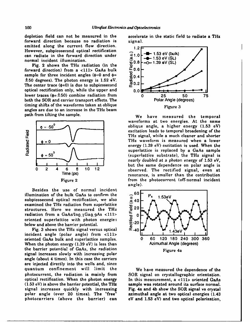
100 Ultrafast Electronics and Optoelectronics
depletion field can not be measured in the accelerate in the static field to radiate a THzforward direction because no radiation is signal.emitted along the current flow direction.However, subpicosecond optical rectificationcan radiate in the forward direction under •.1.0 ,- 1.53 eV (bulk)normal incident illumination. S - 1.53 eV (SL)
Fig. 2 shows the THz radiation (in the 0forward direction) from a <111> GaAs bulk .0.6-
sample for three incident angles (0=0 and 0= • 0.4±50 degrees). The photon energy is 1.52 eV. 20.2
The center trace (0=0) is due to subpicosecond r0 =
optical rectification only, while the upper and 0.0.lower traces (0=±50) combine radiation from 0 25 50 75both the SOR and carrier transport effects. The Polar Angle (degrees)timing shifts of the waveforms taken at oblique Figure 3angles are due to an increase in the THz beampath from tilting the sample. We have measured the temporal
waveforms at two energies. At the same_50° 0 oblique angle, a higher energy (1.53 eV)
excitation leads to temporal broadening of theTHz signal, while a much cleaner and shorteru-THz waveform is measured when a lowerenergy (1.39 eV) excitation is used. When thesuperlattice is replaced by a GaAs sample
cc =50 (superlattice substrate), the THz signal isnearly doubled at a photon energy of 1.53 eV,
l i _ I I I but the same dependence on polar angle is0 2 4 6 8 10 12 observed. The rectified signal, even at
"Time (ps) resonance, is smaller than the contributionFigure 2 from the photocurrent (off-normal incident
angle).Besides the use of normal incident
illumination of the bulk GaAs to confirm the Ps60subpicosecond optical rectification, we also 40examined the THz radiation from superlatticestructures. Here we measured the THz -Z 20radiation from a GaAs/InO.1GaO.9As <111> 0 0oriented superlattice with photon energies -20below and above the barrier potential.
Fig. 3 shows the THz signal versus optical cc-40incident angle (polar angle) from <111>oriented GaAs bulk and superlattice samples. 0 60 120 180 240 300 360When the photon energy (1.39 eV) is less than Azimuthal Angle (degrees)the barrier potential of GaAs, the radiation Figure 4asignal increases slowly with increasing polarangle (about 4 times). In this case the carriersare injected directly into the wells and, sincequantum confinement will limit the We have measured the dependence of thephotocurrent, the radiation is mainly from SOR signal on crystallographic orientation.optical rectification. When the photon energy In this measurement, a <111> oriented GaAs(1.53 eV) is above the barrier potential, the THz sample was rotated around its surface normal.signal increases quickly with increasing Fig. 4a and 4b show the SOR signal vs crystalpolar angle (over 20 times). The "free" azimuthal angle at two optical energies (1.43photocarriers (above the barrier) can eV and 1.53 eV) and two optical polarization,
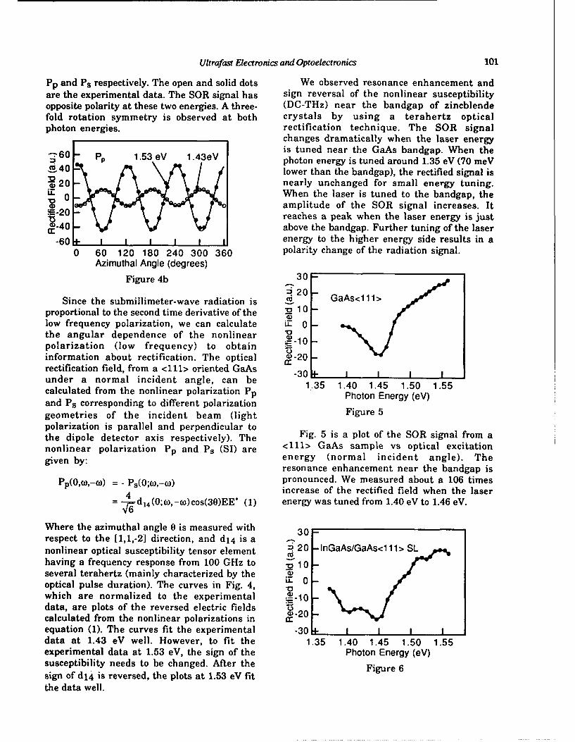
Ultrafast Electronics and Optoelectronics 101
Pp and Ps respectively. The open and solid dots We observed resonance enhancement andare the experimental data. The SOR signal has sign reversal of the nonlinear susceptibilityopposite polarity at these two energies. A three- (DC-THz) near the bandgap of zincblendefold rotation symmetry is observed at both crystals by using a terahertz opticalphoton energies. rectification technique. The SOR signal
changes dramatically when the laser energy"•60 - Pp 1.53 eV 1.43eV is tuned near the GaAs bandgap. When the
S•40• -lower than the bandgap), the rectified signal isS20 nearly unchanged for sm all energy tuning.
U When the laser is tuned to the bandgap, theD 0amplitude of the SOR signal increases. It
reaches a peak when the laser energy is justC-40 above the bandgap. Further tuning of the laser
_60 +- _I _________ I energy to the higher energy side results in a
0 60 120 180 240 300 360 polarity change of the radiation signal.Azimuthal Angle (degrees)
Figure 4b 30 -S20
Since the submillimeter-wave radiation is _6 GaAs<111>proportional to the second time derivative of the 1 0low frequency polarization, we can calculate U_ 0the angular dependence of the nonlinear 10 -1polarization (low frequency) to obtaininformation about rectification. The optical •-20rectification field, from a <111> oriented GaAs -30 +under a normal incident angle, can be 1.35 1.40 1.45 1.50 1.55calculated from the nonlinear polarization Pp Photon Energy (eV)and Ps corresponding to different polarization PhtnEe (geometries of the incident beam (light Figure 5polarization is parallel and perpendicular tothe dipole detector axis respectively). The Fig. 5 is a plot of the SOR signal from anonlinear polarization Pp and Ps (SI) are <111> GaAs sample vs optical excitationgiven by: energy (normal incident angle). The
resonance enhancement near the bandgap ispronounced. We measured about a 106 timesincrease of the rectified field when the laser4d
= �d 14(0;o,-(o)cos(30)EE* (1) energy was tuned from 1.40 eV to 1.46 eV.
Where the azimuthal angle 0 is measured with 30respect to the [1,1,-21 direction, and d 14 is anonlinear optical susceptibility tensor element z 20 InGaAs/GaAs<c111> SLhaving a frequency response from 100 GHz to I0 -several terahertz (mainly characterized by theoptical pulse duration). The curves in Fig. 4, 0
which are normalized to the experimental 2-I0data, are plots of the reversed electric fieldscalculated from the nonlinear polarizations in c-20equation (1). The curves fit the experimental -30 1 1 1 Idata at 1.43 eV well. However, to fit the 1.35 1.40 1.45 1.50 1.55experimental data at 1.53 eV, the sign of the Photon Energy (eV)susceptibility needs to be changed. After the Figure 6sign of d14 is reversed, the plots at 1.53 eV fitthe data well.
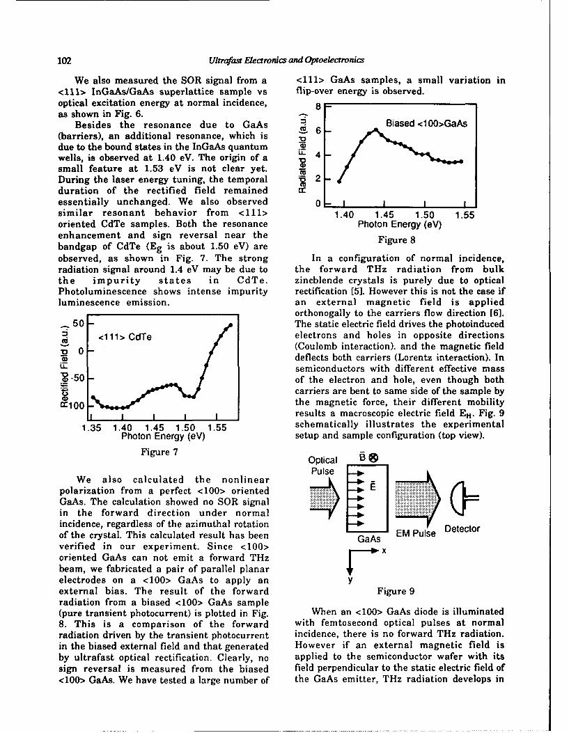
102 Ultrafast Electronics and Optoelectronics
We also measured the SOR signal from a <111> GaAs samples, a small variation in<111> InGaAs/GaAs superlattice sample vs flip-over energy is observed.optical excitation energy at normal incidence, 8as shown in Fig. 6.
Besides the resonance due to GaAs Biased <100>GaAs(barriers), an additional resonance, which is _
due to the bound states in the InGaAs quantumwells, is observed at 1.40 eV. The origin of a " 4 -
small feature at 1.53 eV is not clear yet.During the laser energy tuning, the temporal 2 2duration of the rectified field remained ccessentially unchanged. We also observed 0- l_ _ _ _ _ _
similar resonant behavior from <111> 1.40 1.45 1.50 1.55oriented CdTe samples. Both the resonance Photon Energy (eV)enhancement and sign reversal near the Figure 8bandgap of CdTe (Eg is about 1.50 eV) areobserved, as shown in Fig. 7. The strong In a configuration of normal incidence,radiation signal around 1.4 eV may be due to the forward THz radiation from bulkthe impurity states in CdTe. zincblende crystals is purely due to opticalPhotoluminescence shows intense impurity rectification [5]. However this is not the case ifluminescence emission. an external magnetic field is applied
orthonogally to the carriers flow direction [6].-50- The static electric field drives the photoinduced
<111>CdTe electrons and holes in opposite directionsS0 <- (Coulomb interaction), and the magnetic field
deflects both carriers (Lorentz interaction). InU- semiconductors with different effective mass
-50 - of the electron and hole, even though bothcarriers are bent to same side of the sample by
r00 the magnetic force, their different mobilityC100 I I Iresults a macroscopic electric field EH. Fig. 91.35 1 .40 1.45 1.50 1.55schematically illustrates the experimental
Photon Energy (eV) setup and sample configuration (top view).
Figure 7 pOptical BIPulse -.
We also calculated the nonlinearpolarization from a perfect <100> orientedGaAs. The calculation showed no SOR signal ... -.in the forward direction under normalincidence, regardless of the azimuthal rotation -- cof the crystal. This calculated result has been GaAs EM Pulse Detectorverified in our experiment. Since <100> xoriented GaAs can not emit a forward THzbeam, we fabricated a pair of parallel planarelectrodes on a <100> GaAs to apply an yexternal bias. The result of the forward Figure 9radiation from a biased <100> GaAs sample(pure transient photocurrent) is plotted in Fig. When an <100> GaAs diode is illuminated8. This is a comparison of the forward with femtosecond optical pulses at normalradiation driven by the transient photocurrent incidence, there is no forward THz radiation.in the biased external field and that generated However if an external magnetic field isby ultrafast optical rectification. Clearly, no applied to the semiconductor wafer with itssign reversal is measured from the biased field perpendicular to the static electric field of<100> GaAs. We have tested a large number of the GaAs emitter, THz radiation develops in
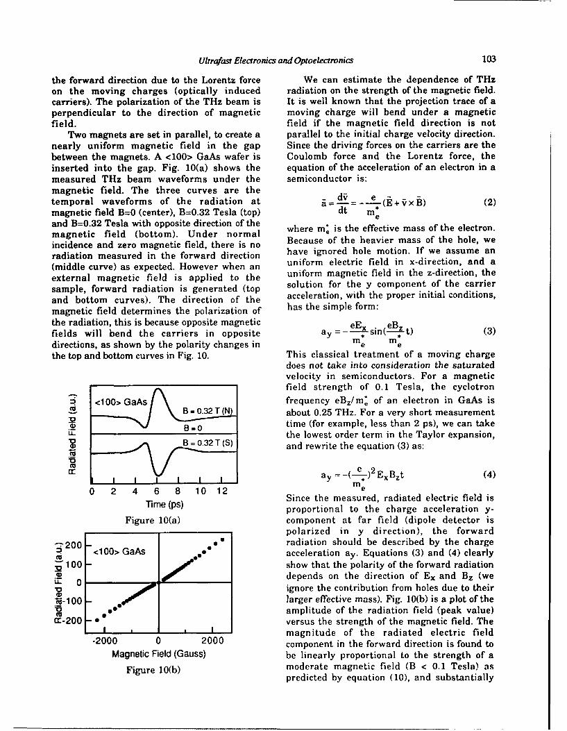
Ultrafost Electronics and Optoelectronics 103
the forward direction due to the Lorentz force We can estimate the dependence of THzon the moving charges (optically induced radiation on the strength of the magnetic field.carriers). The polarization of the THz beam is It is well known that the projection trace of aperpendicular to the direction of magnetic moving charge will bend under a magneticfield. field if the magnetic field direction is not
Two magnets are set in parallel, to create a parallel to the initial charge velocity direction.nearly uniform magnetic field in the gap Since the driving forces on the carriers are thebetween the magnets. A <100> GaAs wafer is Coulomb force and the Lorentz force, theinserted into the gap. Fig. 10(a) shows the equation of the acceleration of an electron in ameasured THz beam waveforms under the semiconductor is:magnetic field. The three curves are thetemporal waveforms of the radiation at aŽ=d=-= e(E+irxB) (2)magnetic field B=0 (center), B=0.32 Tesla (top) dt m*
and B=0.32 Tesla with opposite direction of the
magnetic field (bottom). Under normal where m: is the effective mass of the electron.
incidence and zero magnetic field, there is no Because of the heavier mass of the hole, we
radiation measured in the forward direction have ignored hole motion. If we assume an
(middle curve) as expected. However when an uniform electric field in x-direction, and a
external magnetic field is applied to the uniform magnetic field in the z-direction, the
sample, forward radiation is generated (top solution for the y component of the carrier
and bottom curves). The direction of the acceleration, with the proper initial conditions,
magnetic field determines the polarization of has the simple form:
the radiation, this is because opposite magnetic eEx eBzfields will bend the carriers in opposite ay = ---- sin( t) (3)
directions, as shown by the polarity changes in me methe top and bottom curves in Fig. 10. This classical treatment of a moving charge
does not take into consideration the saturatedvelocity in semiconductors. For a magneticfield strength of 0.1 Tesla, the cyclotron
. <100> GaAs frequency eBz/m: of an electron in GaAs isB 0.32 T (N about 0.25 THz. For a very short measurement
3B time (for example, less than 2 ps), we can takeL.L the lowest order term in the Taylor expansion,
B = 0.32T (S) and rewrite the equation (3) as:
Cucc I ay =-(e ) 2 ExBzt (4)
0 2 4 6 8 10 12 e
Time (ps) Since the measured, radiated electric field isproportional to the charge acceleration y-
Figure 10(a) component at far field (dipole detector ispolarized in y direction), the forward
-200 radiation should be described by the charge6 <100> GaAs acceleration ay. Equations (3) and (4) clearly
i' 100 - show that the polarity of the forward radiation..) depends on the direction of Ex and Bz (we
ignore the contribution from holes due to their
*-100 _ larger effective mass). Fig. 10(b) is a plot of theamplitude of the radiation field (peak value)
crc200 - versus the strength of the magnetic field. The! , I magnitude of the radiated electric field
-2000 0 2000 component in the forward direction is found to
Magnetic Field (Gauss) be linearly proportional to the strength of a
Figure 10(b) moderate magnetic field (B < 0.1 Tesla) aspredicted by equation (10), and substantially
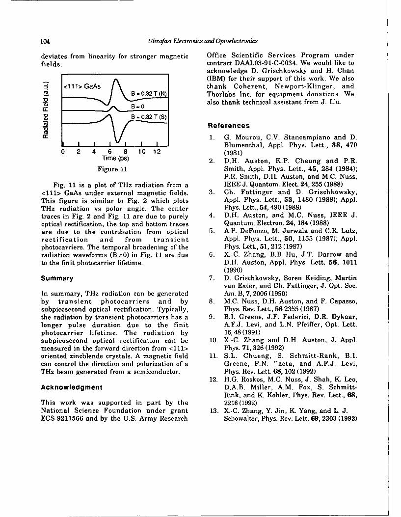
104 Ultrafast Electronics and Optoelectronics
deviates from linearity for stronger magnetic Office Scientific Services Program underfields. contract DAAL03-91-C-0034. We would like to
acknowledge D. Grischkowsky and H. Chan(IBM) for their support of this work. We also
i-• <1 1 1>GaAs [ thank Coherent, Newport-Klinger, andSB=0.32T(N) Thorlabs Inc. for equipm ent donations. W e
B.0 • also thank technical assistant from J. L'u.
"o B =- 0.32 T (S)
References
a: 1. G. Mourou, C.V. Stancampiano and D.Blumenthal, Appl. Phys. Lett., 38, 470
0 2 4 6 8 10 12 (1981)Time (ps) 2. D.H. Auston, K.P. Cheung and P.R.
Figure 11 Smith, Appl. Phys. Lett., 45, 284 (1984);P.R. Smith, D.H. Auston, and M.C. Nuss,
Fig. 11 is a plot of TfIz radiation from a IEEEJ. Quantum. Elect. 24,255 (1988)<111> GaAs under external magnetic fields. 3. Ch. Fattinger and D. Grischkowsky,This figure is similar to Fig. 2 which plots Appl. Phys. Lett., 53, 1480 (1988); Appl.THz radiation vs polar angle. The center Phys. Lett., 54,490 (1988)traces in Fig. 2 and Fig. 11 are due to purely 4. D.H. Auston, and M.C. Nuss, IEEE J.optical rectification, the top and bottom traces Quantum. Electron. 24, 184 (1988)are due to the contribution from optical 5. A.P. DeFonzo, M. Jarwala and C.R. Lutz,rectification and from transient Appl. Phys. Lett., 50, 1155 (1987); Appl.photocarriers. The temporal broadening of the Phys. Lett., 51, 212 (1987)radiation waveforms (B•0) in Fig. 11 are due 6. X.-C. Zhang, B.B Hu, J.T. Darrow andto the finit photocarrier lifetime. D.H. Auston, Appl. Phys. Lett. 56, 1011
(1990)Summary 7. D. Grischkowsky, Soren Keiding, Martin
van Exter, and Ch. Fattinger, J. Opt. Soc.In summary, THz radiation can be generated Am. B, 7,2006 (1990)by transient photocarriers and by 8. M.C. Nuss, D.H. Auston, and F. Capasso,subpicosecond optical rectification. Typically, Phys. Rev. Lett., 58 2355 (1987)the radiation by transient photocarriers has a 9. B.I. Greene, J.F. Federici, D.R. Dykaar,longer pulse duration due to the finit A.F.J. Levi, and L.N. Pfeiffer, Opt. Lett.photocarrier lifetime. The radiation by 16,48(1991)subpicosecond optical rectification can be 10. X.-C. Zhang and D.H. Auston, J. Appl.measured in the forward direction from <111> Phys. 71,326 (1992)oriented zincblende crystals. A magnetic field 11. S.L. Chueng, S. Schmitt-Rank, B.I.can control the direction and polarization of a Greene, P.N. "aeta, and A.F.J. Levi,THz beam generated from a semiconductor. Phys. Rev. Lett. 68, 102 (1992)
12. H.G. Roskos, M.C. Nuss, J. Shah, K. Leo,Acknowledgment D.A.B. Miller, A.M. Fox, S. Schmitt-
Rink, and K. Kohler, Phys. Rev. Lett., 68,This work was supported in part by the 2216(1992)National Science Foundation under grant 13. X.-C. Zhang, Y. Jin, K. Yang, and L. J.ECS-9211566 and by the U.S. Army Research Schowalter, Phys. Rev. Lett. 69, 2303 (1992)
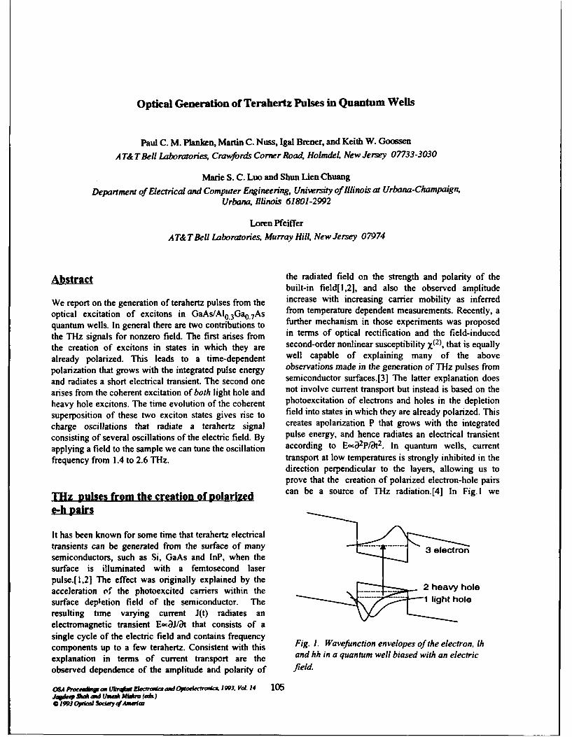
Optical Generation of Terahertz Pulses in Quantum Wells
Paul C. M. Planken, Martin C. Nuss, Igal Brener, and Keith W. Goossen
A T& TBell Laboratories, Crawfords Corner Road, HolmdeL New Jersey 07733-3030
Marie S. C. Luo and Shun Lien Chuang
Department of Electrical and Computer Engineering, University of Illinois at Urbana-Champaign,Urbana, Illinois 61801-2992
Loren Pfeiffer
AT&T Bell Laboratories, Murray Hill, New Jersey 07974
Abstract the radiated field on the strength and polarity of thebuilt-in field[1,2], and also the observed amplitude
We report on the generation of terahertz pulses from the increase with increasing carrier mobility as inferred
optical excitation of excitons in GaAs/AI0 .3Gao.7 As from temperature dependent measurements. Recently, a
quantum wells. In general there are two contributions to further mechanism in those experiments was proposed
the THz signals for nonzero field. The first arises from in terms of optical rectification and the field-induced
the creation of excitons in states in which they are second-order nonlinear susceptibility X(2), that is equally
already polarized. This leads to a time-dependent well capable of explaining many of the above
polarization that grows with the integrated pulse energy observations made in the generation of THz pulses from
and radiates a short electrical transient. The second one semiconductor surfaces.[3] The latter explanation does
arises from the coherent excitation of both light hole and not involve current transport but instead is based on the
heavy hole excitons. The time evolution of the coherent photoexcitation of electrons and holes in the depletion
superposition of these two exciton states gives rise to field into states in which they are already polarized. This
charge oscillations that radiate a terahertz signal creates apolarization P that grows with the integrated
consisting of several oscillations of the electric field. By pulse energy, and hence radiates an electrical transient
applying a field to the sample we can tune the oscillation according to Eoc-P/&t2 . In quantum wells, current
frequency from 1.4 to 2.6 THz. transport at low temperatures is strongly inhibited in thedirection perpendicular to the layers, allowing us toprove that the creation of polarized electron-hole pairs
THz pulses from the creation of polarized can be a source of THz radiation.[4] In Fig. I we
It has been known for some time that terahertz electricaltransients can be generated from the surface of many 3 electronsemiconductors, such as Si, GaAs and InP, when the
surface is illuminated with a femtosecond laserpulse.[l,21 The effect was originally explained by theacceleration of the photoexcited carriers within the 22 heavy hole
surface depletion field of the semiconductor. The 1 light hole
resulting time varying current J(t) radiates anelectromagnetic transient E-aJ/cJt that consists of asingle cycle of the electric field and contains frequencycomponents up to a few terahertz. Consistent with this Fig. 1. Wavefunction envelopes of the electron, lh
explanation in terms of current transport are the and hh in a quantum well biased with an electric
observed dependence of the amplitude and polarity of field.
oSA PAoceag m U/r~f Ekffmkt s and OEperFOeaRo 1993. VoL 14 105Jqdq Mak md Unm MdAm (eak)* 1993 Opdod Sade ofAxwuea
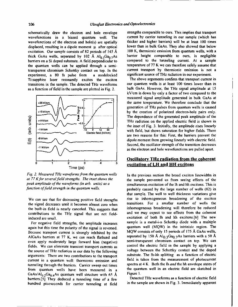
106 Ultrafast Electronics and Optoelectronics
schematically draw the electron and hole envelope strengths comparable to ours. This implies that transportwavefunctions in a biased quantum well. The current by carrier tunneling in our sample (which haswavefunctions of the electron and hole(s) are spatially thicker and higher barriers) will be at least 100 timesdisplaced, resulting in a dipole moment g after optical lower than in bulk GaAs. They also showed that belowexcitation. Our sample consists of 82 periods of 145 A 100 K, thermionic emission from quantum wells, with athick GaAs wells, separated by 102 A Al0.3Gao.7 As barrier height comparable to ours, is negligiblebarriers on a Si doped substrate. A field perpendicular to compared to the tunneling current. At a samplethe quantum wells can be applied through a semi- temperature of 77 K we can therefore safely assume thattransparent chromium Schottky contact on top. In the current transport by thermionic emission is not aexperiment, a 80 fs pulse from a modelocked significant source of THz radiation in our experiment.Ti:sapphire laser resonantly excites the exciton The above arguments confirm that transport current intransitions in the sample. The detected THz waveforms our quantum wells is at least 100 times lower than inas a function of field in the sample are plotted in Fig. 2. bulk GaAs. However, the TIz signal amplitude at 15
kV/cm is down by only a factor of two compared to themeasured signal amplitude generated in bulk GaAs at
•25SkV/cmr the same temperature. We therefore conclude that the* •.s generation of THz pulses from quantum wells is caused
+15 kV/cm•n - by the creation of polarized electron-hole pairs only.- o. The dependence of the generated peak amplitude of the
-+4kV/n .THz radiation on the applied electric field is shown in/0.5- the inset of Fig. 3. Initially, the amplitude rises linearlyEc1 kV/. r1 0 ie k/ with field, but shows saturation for higher fields. Thereare two reasons for this: First, the barriers prevent the
-6 "kv/Cr -dipole moment from growing linearly with electric field.Second, the oscillator strength of the transition decreasesas the electron and hole wavefunctions are pulled apart.
Oscillatory THz radiation from the coherent1 2 3 excitation of LH and HH excitonsTime (ps)
Fig. 2. Measured THz waveformsfrom the quantum wells In the previous section the broad exciton linewidths inat 77 Kfor several field strengths. The inset shows the the sample prevented us from seeing effects of thepeak amplitude of the waveforms (in arb. units) as a simultaneous excitation of the Ih and hh excitons. This isfunction offield strength in the quantum wells, probably caused by the large number of wells (82) in
that sample. The well to well thickness variations giveWe can see that for decreasing positive field strengths rise to inhomogeneous broadening of the excitonthe signal decreases until it becomes almost zero when transitions. For a smaller number of wells thethe built-in field is nearly canceled. This suggests that inhomogeneous broadening will therefore be reducedcontributions to the THz signal that are not field- and we may expect to see effects from the coherentinduced are small. excitation of both lh and hh excitons.[6] The new
For negative field strengths, the amplitude increases sample is a metal-i-n Schottky diode with a multipleagain but this time the polarity of the signal is reversed, quantum well (MQW) in the intrinisic region. TheBecause transport current is strongly inhibited by the MQW consists of only 15 periods of 175 A GaAs wells,AIGaAs barriers at 77 K, we can reach flatband and separated by 150 A AI0.3 Ga 0 .7 As barriers with a 50 Aeven apply moderately large forward bias (negative) semi-transparent chromium contact on top. We canfields. We can eliminate transient transport currents as control the electric field in the sample by applying athe source of THz radiation in our data by the following voltage between the Schottky contact and the dopedarguments: There are two contributions to the transport substrate. The Ih-hh splitting as a function of electriccurrent in a quantum well: thermionic emission and field is taken from the measurement of photocurrenttunneling through the barriers. Carrier sweep out times spectra at 4 K. Both the lh and the hh envelope states offrom quantum wells have been measured in a the quantum well in an electric field are sketched inGaAs/Al0 2Ga0o.As quantum well structure with 65 A Figure 1.barriers.J5] They deduced a tunneling time of a few Detected THz waveforms as a function of electric fieldhundred picoseconds for carrier tunneling at field in the sample are shown in Fig. 3. Immediately apparent
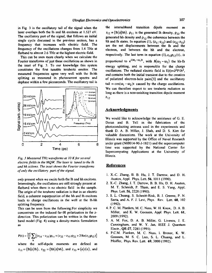
Ultrafast Electronics and Optoelectronics 107
in Fig. 3 is the oscillatory tail of the signal when the the intersubband transition dipole moment aslaser overlaps both the lh and hh excitons at 1.527 eV. z12 = (hlzlhh). PuI is the generated lh density, P22 theThe oscillatory part of the signal, that follows an initial generated hh density and P12 the coherence between thesingle cycle discussed in the previous section, has a hh and Ih states. In equation (I), (Z l-Z3 3 ) and (z 2 2 -z 3 3 )
frequency that increases with electric field. The are the net displacements between the lh and thefrequency of the oscillations changes from 1.4 THz at electron, and between the hh and the electron,flatband to almost 2.6 THz at the highest electric field. respectively. The last term in equation (I),Zl2P12(t), is
This can be seen more clearly when we calculate theFourier transforms of just these oscillations as shown in proportional to ei(W2-W)t, with h(W2 -( 1 ) the hh-lhthe inset of Fig. 3. To our knowledge this system energy splitting, and is responsible for the chargeconstitutes the first tunable terahertz emitter. The oscillations. The radiated electric field is E(t)oea2 p/at 2,measured frequencies agree very well with the lh-hh and contains both the initial transient due to the creationsplitting as measured in photocurrent spectra and of polarized electron-hole pairs[3] and the oscillatorydephase within a few picoseconds. The oscillatory tail is tail - cos(co 1 - (2)t caused by the charge oscillations.
We can therefore expect to see terahertz radiation as33k./cm -,0v c-, long as there is a nonvanishing transition dipole moment
33 kV/cm.1 *t4 . - 26,vMcm z]2.S/ ~~~ ...\";.-"33 kV/cm
.~2 2kV/cm 0 : .
-, ,.. Acknowledgments19 kV/cm
0 -- • 2 3 We would like to acknowledge the assistance of G. E.
"15 kV/cm Freauency (THz) Doran and B. Tell in the fabrication of thephotoconducting antenna used in the experiments and
OkV thank D. A. B. Miller, J. Shah, and D. S. Kim for0 /valuable discussions. The work at the University of
Illinois was supported by the Office of Naval Research
0 2 4 6 8 under grant (N00014-90-J-1821) and the supercomputer
Time (ps) time was supported by the National Center forSupercomputing Applications at the University of
Fig. 3 Measured THz waveforms at 10 Kfor several Illinois.
electric fields in the MQW. The laser is tuned to the lhand hh xcitons. The inset shows the Fourier transforms Referencesof only the oscillatory part of the signal.
I. X.-C. Zhang, B. B. Hu, J. T. Darrow, and D. H.
only present when we excite both the Ih and hh excitons. Auston, Appl. Phys. Lett. 56, 1011 (1990).Interestingly, the oscillations are still strongly present at 2. X.-C. Zhang, J. T. Darrow, B. B. Hu, D. H. Auston,flatband when there is no electric field in the sample. M. T. Schmidt, P. Tham, and E. S. Yang, Appl.The origin of the terahertz radiation is that in an electric Phys. Lett. 56, 2228 (1990).field, a coherent superposition of the hh and lh excitons 3. S. L. Chuang, S. Schmitt-Rink, B. 1. Greene, P. N.leads to charge oscillations in the well at the lh-hh Saeta, and A. F. J. Levi, Phys. Rev. Lett. 68, 102splitting frequency. (1992).This can be seen from the following:For simplicity we 4. P. C. M. Planken, M. C. Nuss, W. H. Knox, D. A. B.concentrate on the induced far-IR polarization in the z- Miller, and K. W. Goossen, Appl. Phys. Lett. 61,direction. This polarization can be written in the three- 2009 (1992).band model (Fig. 4) using a density-matrix formulation 5. A. M. Fox, D. A. B. Miller, G. Livescu, J. E.as Cunningham, and W. Y. Jan, IEEE J. Quantum
Electr., QE-27, 2281 (199 1).lel-,(__, 1 6. P.C.M. Planken, M. C. Nuss, I. Brener, K. W.
P(t) =--V ,[(z I-z33)P I+(Z22-z3)P22+2Re(z12P12)] Goossen, M. S. C. Luo, S. L. Chuang, and L.k Pfeiffer, Phys. Rev. Lett. 69, 3800 (1992).
where the self-dipole moments are defined as
z,, = (lhIzIlh), Z22 = (hhlzlhh), and z33 =(elzle), and
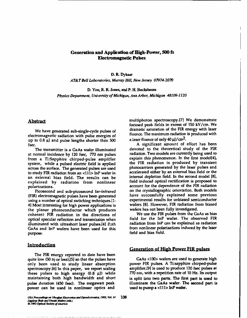
Generation and Application of High-Power, 500 fsElectromagnetic Pubes
D. R. Dykar
AT& TBell Laboratories, Murray Hill New Jersey 07974-2070
D. You, R. R. Jones, and P. H. Bucksbaum
Physics Department, University of Michigan, Ann Arbor, Michigan 48109-1120
Abstract multiphoton spectroscopy.[71 We demonstratefocused peak fields in excess of 150 kV/cm. We
We have generated sub-single-cycle pulses of dramatic saturation of the FIR energy with laser
electromagnetic radiation with pulse energies of fluence. The maximum radiation is produced with
up to 0.8 ptJ and pulse lengths shorter than 500 a laser fluence of only 40 gLJ/cm 2 .fsec. A significant amount of effort has been
The transmitter is a GaAs wafer illuminated devoted to the theoretical study of the FIRat normal incidence by 120 fsec, 770 nm pulses radiation. Two models are currently being used tofrom a Ti:Sapphire chirped-pulse amplifier explain this phenomenon. In the first model[4],system, while a pulsed electric field is applied the FIR radiation is produced by transientacross the surface. The generated pulses are used photocarriers generated by the laser pulses andto study FIR radiation from an <111> InP wafer in accelerated either by an external bias field or thean external bias field. The results can be internal depletion field. In the second model [81,explained by radiation from nonlinear field induced optical rectification is proposed topolarizations, account for the dependence of the FIR radiation
Picosecond and sub-picosecond far-infrared on the crystallographic orientation. Both models(FIR) electromagnetic pulses have been generated have successfully explained some previoususing a number of optical switching techniques.[f- experimental results for unbiased semiconductor4] Most interesting for high power applications is wafers [8]. However, FIR radiation from biasedthe planar photoconductor which produces wafers has not been fully investigated.coherent FIR radiation in the directions of We use the FIR pulses from the GaAs as biasoptical specular reflection and transmission when field for the InP wafer. The observed FIRilluminated with ultrashort laser pulses.[4] Both radiation from InP can be explained as radiationGaAs and InP wafers have been used for this from nonlinear polarizations induced by the laserpurpose. field and bias field.
IntroductionGeneration of High Power FIR pulses
The FIR energy reported to date have beenquite low (50 nj or less),[51 so that the pulses have GaAs <100> wafers are used to generate highonly been used to study linear absorption power FIR pulses. A Ti:sapphire chirped-pulsespectroscopy.f6] In this paper, we report scaling amplifier,[91 is used to produce 120 fsec pulses atthese pulses to high energy (0.8 ILJ) while 770 nm, with a repetition rate of 10 Hz. Its outputmaintaining both high bandwidth and short is split into two parts. The first part is used topulse duration (450 fsec). The megawatt peak illuminate the GaAs wafer. The second part ispower can be used in nonlinear optics and used to pump a < 11> InP wafer.
OSA P•ceaWpon Ukiu kme aWarOoekaro t1993, VoL.4 108Joqoep SaA and Unesh UL•m (a•d)* 1993 Op"ica Soda 1Y9Amaesk
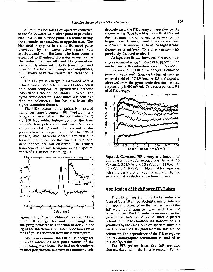
Ultrafast Electronics and Optoelectronics 109
Aluminum electrodes 1 cm apart are connected dependence of the FIR energy on laser fluence. Asto the GaAs wafer with silver paint to provide a shown in Fig. 2, at low bias fields (E1<4 kV/cm)bias field in the surface plane. To reduce arcing the maximum FIR pulse energy occurs for thethe electrodes are attached to opposite faces. The largest laser fluence, and there is no clearbias field is applied in a slow (50 j.sec) pulse evidence of saturation, even at the highest laserprovided by an automotive spark coil fluence of 2 mJ/cm2 . This is consistent withsynchronized with the laser. The laser beam is previously observed results.[4]expanded to illuminate the wafer as well as the At high bias fields, however, the maximumelectrodes to obtain efficient FIR generation. energy occurs at a laser fluence of 40 gj/cm2 . TheRadiation is observed in both transmitted and mechanism for this saturation is not understood.reflected directions with comnparable amplitudes, The maximum FIR pulse energy is obtainedbut usually only the transmitted radiation is from a 3.5x3.5 cm 2 GaAs wafer biased with anused. external field of 10.7 kV/cm. A 425 mV signal is
The FIR pulse energy is measured with a observed from the pyroelectric detector, whose
helium cooled bolometer (Infrared Laboratories) obseved m the ctricpdetec to whsor aroo temeraurepyrolecric etetor responsivity is 490 mY/14J. This corresponds to 0.8or a room temperature pyroelectric detector gJ of FIRenergy.(Molectron Detector, Inc., model P1-42cc). Thepyroelectric detector is 300 times less sensitive I I I ,than the bolometer, but has a substantiallyhigher saturation fluence. U) 10,
The FIR spectrum of our pulses is measured , ý"0 .using an interferometer.[10] Typical inter-ferograms measured with the bolometer (Fig. 1) 0 %are 600 fsec wide, independent of the laser >, Iintensity, laser polarization and bias field. For a 10-3<100> crystal (GaAs) the second order C :W'•
polarization is perpendicular to the crystalsurface, and therefore doesn't contribute toforward radiation so the various relationaldependances are not observed. The Fourier L 0 0 0 0 20.00 0.05 0.10 0.15 0.20 0.25 0.30
transform of the interferogram yields a spectral Loser Fluence (mJ/cm2 )
width of 1 THz (see inset in Fig. 1).
1.0 .. ................. Figure 2. Generated FIR energy as a function ofpump laser fluence for selected bias fields. 0: 1.5kV/cm; A: 3.0 kV/cm; +: 4.5 kV/cm; X: 6 kV/cm; 0:•,0.8
"0.8 7.5 kV/cm; *: 9 kV/cm. Note that for large biasfields there is a pronounced maximum in the FIR
0 .6 o generation at a relatively low laser fluence.,00 1.5 3.0
20.4"Application of High Power FIR Pulses
c 0.2 The FIR pulses from the GaAs wafer are
focused by a 10 cm paraboloidal mirror into a 40.0 .. . . . . .. . .. . mm spot and projected on the front surface of the
6 -2 0 2 4 6 InP wafer as a transient bias field. The FIRDelay (ps) radiation from the lnP wafer is measured in the
Figure I. Interferogram obtained by collecting the transmitted direction. A spatial filter is placedtotal FIR energy transmitted through the behind the lnP to eliminate the transmitted FIRanalyzing polarizer as a function of delay in one produced by the GaAs. A 25 cm spherical mirror isleg of the interferometer. Inset: Spectrum F(v) of used to focus the FIR signals from the InP into thethe FIR pulses obtained from the interferogram. bolometer. The dependence of the FIR energy on
We have examined the FIR pulse energy for the crystallographic orientation is studied indifferent intensities and polarizations of the this configuration.illuminating laser beam. We find no dependence The FIR pulses from the InP are alsoon laser polarization, but there is a nonmonotonic characterized with the interferometer. For an
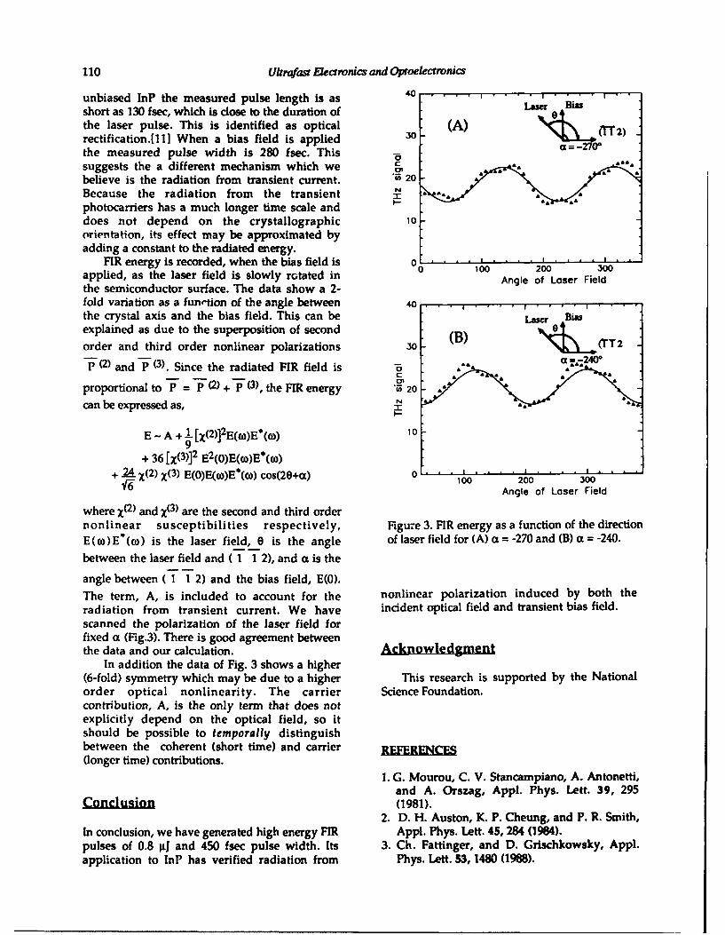
110 Uktra aost Eledronac and Optoelectronics
unbiased InP the measured pulse length is as L0 Binshort as 130 fsec, which is close to the duration ofas Biasthe laser pulse. This is identified as optical (A) 2)rectification.[l1l When a bias field is applied (rthe measured pulse width is 280 fsec. Thissuggests the a different mechanism which we &believe is the radiation from transient current. 20Because the radiation from the transientphotocarriers has a much longer time scale anddoes not depend on the crystallographic 10orientation, its effect may be approximated byadding a constant to the radiated energy.
FIR energy is recorded, when the bias field is 0applied, as the laser field is slowly rotated in Anl of L00the semiconductor surface. The data show a 2- Angle of Loser Fieldfold variation as a fun,-tion of the angle between 40 . . . . .the crystal axis and the bias field. This can be Laser Biasexplained as due to the superposition of second (B)order and third order nonlinear polarizations 30 (TT2
P( 2) and P (3). Since the radiated FIR field is -
proportional to P = P (2 ) + p (3), the FIR energy "0 20Ncan be expressed as,
E - A + 1 [X(2)]2 E'coE*(0 109
+ 36 [X(3)]2 E2 (0)E((o)E*(ao)+ .24 X(2) X(3) E()E(0))Ee((o) cos(20+ot) 0 .100 200 300
Angle of Laser Field
where X(2) and x(3) are the second and third ordernonlinear susceptibilities respectively, Figu'e 3. FIR energy as a function of the directionE(0)E*(m) is the laser field, 0 is the angle of laser field for (A) z = -270 and (B) a = -240.
between the laser field and ( 1 1 2), and a is the
angle between ( 1 1 2) and the bias field, E(0).
The term, A, is included to account for the nonlinear polarization induced by both theradiation from transient current. We have incident optical field and transient bias field.scanned the polarization of the laser field forfixed a (Fig.3). There is good agreement betweenthe data and our calculation. Acknowledgment
In addition the data of Fig. 3 shows a higher(6-fold) symmetry which may be due to a higher This research is supported by the Nationalorder optical nonlinearity. The carrier Science Foundation.contribution, A, is the only term that does notexplicitly depend on the optical field, so itshould be possible to temporally distinguishbetween the coherent (short time) and carrier R EE E.(longer time) contributions.
1. G. Mourou, C. V. Stancampiano, A. Antonetti,and A. Orszag, Appl. Phys. Lett. 39, 295
Concuion (1981).2. D. H. Auston, K. P. Cheung, and P. R. Smith,
In conclusion, we have generated high energy FIR Appl. Phys. Lett. 45, 284 (1984).pulses of 0.8 gJ and 450 fsec pulse width. Its 3. Ch. Fattinger, and D. Grischkowsky, Appl.application to InP has verified radiation from Phys. Lett. 53, 1480 (1988).
Ultrafast Electronics and Optoelectronics il
4. Justin T. Darrow, Xi-Cheng Zhang, David J. 8. S. L. Chuang, S. Schmitt-Rink, B. I. Greene, andAuston, IEEE J. Quantum Electron. 28, 1607 A. F. J. Levi, Phys. Rev. Lett. 68, 102 (1991).(1992). 9. J. Squier, F. Salin, G. Mourou, and D. Harter,
5. B. I. Greene, P. N. Saeta, D. R. Dykaar, S. Opt. Lett. 16, 324 (1991).Schmidt-Rink, and S. L. Chuang, IEEE J. 10 . B. I. Greene, J. F. Federici, D. R. Dykaar, R. R.Quantum Electron. 28,2302 (1992). Jones, and P. H. Bucksbaum, Appl. Phys. Lett.
6. D. Grischkowsky, Soren Keiding, Martin van 59, 893 (1991).Exter, and Ch. Fattinger, J. Opt. Soc. Am.B 7, 11. X. -C. Zhang, Y. Jin, K. Yang, and L. J.2006 (1992). Schowalter, Phys. Rev. Lett. 69, 2303 (1992).
7. R. R. Jones, D. You, and P. H. Bucksbaum,Submitted to Phys. Rev. Lett. (1992).
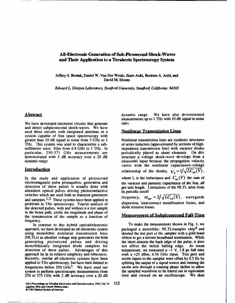
AU-Electronic Generation of Sub-Picosecond Shock-Wavesand Their Application to a Terahertz Spectroscopy System
Jeffrey S. Bostak, Daniel W. Van Der Weide, Ikuro Aoki, Bertram A. Auld, andDavid M. Bloom
Edward L Ginzton Laboraory, Stanford University, Stanford California 94305
Abstract dynamic range. We have also demonstratedmeasurements up to 1 THz with 10 dB signal to noise
We have developed electronic circuits that generate ratio.and detect subpicosecond shock-waves. We haveused these circuits with integrated antennas in a Nonlinear Transmission Linessystem capable of free space spectroscopy withgreater than 10 dB signal to noise from 5 GHz to I Nonlinear transmission lines are synthetic structuresTHz. This system was used to characterize a sub- of series inductors (approximated by sections of high-millimeter wave filter from 6.4 GHz to 1 THz. In impedance transmission line) with varactor diodesparticular, 250-375 GHz measurements are periodically placed as shunt elements. On thisdemonstrated with 2 dB accuracy over a 20 dB structure a voltage shock-wave develops from adynamic range. sinusoidal input because the propagation velocity
varies with the nonlinear capacitance-voltageIntrodU ction relationship of the diodes, VP = 1/ /LC, 1 (V),
In the study and application of picosecond where L is the inductance and Coz(V) the sum ofelectromagnetic pulse propagation, generation and the varactor and parasitic capacitance of the line, alldetection of these pulses is usually done with per unit length. Limitations of the NLTL arise fromultrashort optical pulses driving photoconductive its periodic cutoffswitches which are used both as transient generators frequency, 0), waveguideand samplers. 1 ,2 These systems have been applied toproblems in THz spectroscopy. Fourier analysis of dispersion, interconnect metallization losses, andthe detected pulses, with and without a a test sample diode resistive losses.in the beam path, yields the magnitude and phase ofthe transmission of the sample as a function of Measurement of Subpicosecond Fall-Timefrequency.
In contrast to this hybrid optical/electronic To make the measurement shown in Fig. 1, weapproach, we have developed an all-electronic system packaged a monolithi,- NLTL/sampler chip4 andusing monolithic nonlinear transmission lines shorted the test port of the sampler with a gold bond(NLTLs) as ultrafast voltage step generators for both ribbon to get a known broadband termination. Whilegenerating picosecond pulses and driving the short distorts the back edge of the pulse, it doesmonolithically integrated diode samplers for not affect the initial falling edge. At roomdetection of these pulses. Advantages of this temperature, we measured a -1 V, 1.8 ps fall timeapproach lie in its relative simplicity and robustness. with a +25 dBm, 6.56 GHz input. Test port andRecently, similar all-electronic systems have been strobe inputs to the sampler were offset by 0.5 Hz byapplied to THz spectroscopy, but have been limited to splitting the output of a signal source and running thefrequencies below 250 GHz3 . We have used our strobe arm through a rotating phase shifter to allowsystem to perform spectroscopic measurements from the sampled waveform to be traced out in equivalent250 to 375 GHz with 2 dB accuracy over a 20 dB time and viewed on an oscilloscope. We then
oSA P",cea, on Uttaw Ekrons aid Opoarokcsn 1993. VoL 14 112Ja1dep Oa• ad VoVtr MvAt (Ak)0 1993 O1eWSwkdY afAm~a~e
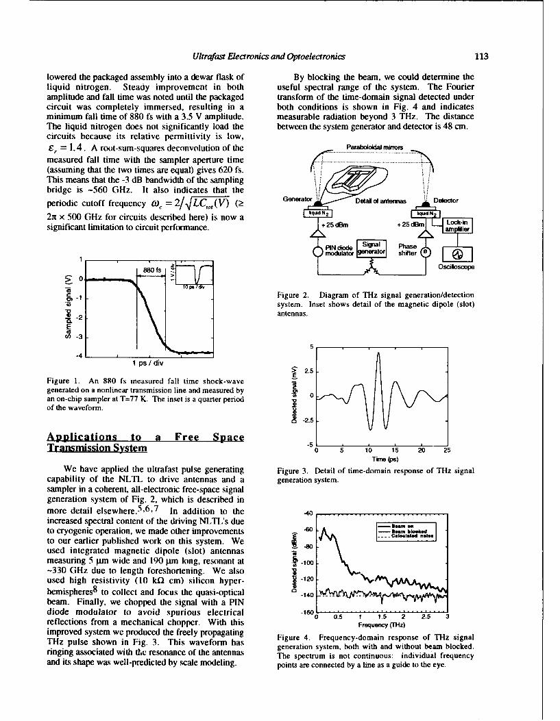
Ultrafast Electronics and Optoelectronics 113
lowered the packaged assembly into a dewar flask of By blocking the beam, we could determine theliquid nitrogen. Steady improvement in both useful spectral range of the system. The Fourieramplitude and fall time was noted until the packaged transform of the time-domain signal detected undercircuit was completely immersed, resulting in a both conditions is shown in Fig. 4 and indicatesminimum fall time of 880 fs with a 3.5 V amplitude, measurable radiation beyond 3 THz. The distanceThe liquid nitrogen does not significantly load the between the system generator and detector is 48 cm.circuits because its relative permittivity is low,Er = 1.4. A root-sum-squares deconvolution of the ParabIoodal mirrors
measured fall time with the sampler aperture time .(assuming that the two times are equal) gives 620 fs. ...
This means that the -3 dB bandwidth of the samplingbridge is -560 GHz. It also indicates that theperiodic cutoff frequency CO, = LC (V) (_ GonerD o Detector
2nr x 500 GHz for circuits described here) is now a hq-••dN2 S- aN
significant limitation to circuit performance. a 25 dm +25di
PIN diode Signal Phs1 modulator a shiter 0
880fIs ~Ocls
.• -1 Figure 2. Diagram of THz signal generation/detectionsystem. Inset shows detail of the magnetic dipole (slot)
"g-2 antennas.
ECO -3
5-41
1 ps div2.5
Figure 1. An 880 fs measured fall time shock-wavegenerated on a nonlinear transmission line and measured by A? 0an on-chip sampler at T=77 K. The inset is a quarter periodof the waveform.
S-2.5
Applications to a Free Space .5Transmission System 0 5 1 . 5 20 25
Time (ps)
We have applied the ultrafast pulse generating Figure 3. Detail of time-domain response of THz signalcapability of the NLTL to drive antennas and a generation system.sampler in a coherent, all-electronic free-space signalgeneration system of Fig. 2, which is described inmore detail elsewhere. 5 ,6, 7 In addition to the -40increased spectral content of the driving NLTL's due Bocmedto cryogenic operation, we made other improvements -6 ,.ok•".to our earlier published work on this system. We Mused integrated magnetic dipole (slot) antennasmeasuring 5 pm wide and 190 pmn long, resonant at .5.100-330 GHz due to length foreshortening. We alsoused high resistivity (10 kfl cm) silicon hyper- -120
hemispheres 8 to collect and focus the quasi-optical .140beam. Finally, we chopped the signal with a PINdiode modulator to avoid spurious electrical "1600" 0.5 1 1.5 2 2.5 3reflections from a mechanical chopper. With this Frequency (THz)improved system we produced the freely propagating Figure 4. Frequency-domain response of THz signalTHz pulse shown in Fig. 3. This waveform has generation system, both with and without beam blocked.ringing associated with the resonance of the antennas The spectrum is not continuous: individual frequencyand its shape was well-predicted by scale modeling, points are connected by a line as a guide to the eye.
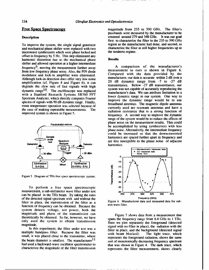
114 Ultrafast Electronics and Optoelectronics
Free Space Spectroscopy magnitude from 235 to 390 GHz. The filter'spassbands were measured by the manufacturer to be
Description centered around 279 and 348 GHz. It was our goalfirst to characterize the filter in the 235 to 390 GHz
To improve the system, the single signal generator region as the manufacturer had done, and second, toand mechanical phase shifter were replaced with two characterize the filter at still higher frequencies up tomicrowave synthesizers which were phase locked and the terahertz regime.offset in frequency by 5 Hz. This step eliminated anyharmonic distortion due to the mechanical phase Resultsshifter and allowed operation at a higher intermediatefrequency 9 , moving the measurement further away A comparison of the manufacturer sfrom low frequency phase noise. Also, the PIN diode measurement to ours is shown in Figure 6.modulator and lock-in amplifier were eliminated. Compared with the data provided by theAlthough lock-in detection does offer very low noise manufacturer, our data is accurate within 2 dB over aAltouh ockindeectondos ofe vry ownose 20 dB dynamic range from -7 to -27 dBamplification (cf. Figure 4 and Figure 6), it can 20adBidync re fo 7 -27 dBdegrade the slew rate of fast signals with high transmittance. Below -27 dB transmittance, our
system was not capable of accurately reproducing thedynamic range 1 0 . The oscilloscope was replaced manufacturer's data. We can attribute limitation to awith a Stanford Research Systems SR760 FFT lower dynamic range in our system. One way toSpectrum Analyzer, which directly computes Fourier improve the dynamic range would be to usespectra of signals with 90 dB dynamic range. Finally, broadband antennas. The magnetic dipole antennasroom temperature operation was selected because of currently used are resonant antennas and have athe ease of making repeatable measurements. The radiation resistance that is a strong function ofimproved system is shown in Figure 5. frequency. A second way to improve the dynamic
range of the system would be to reduce the effects of
Paraboloidal mirrors phase noise on the measurement results. This couldbe accomplished by using synthesizers with less
..................... phase noise. Alternatively, the intermediate frequencycould be increased so that the downconverted
Samnple harmonics are spaced further apart in frequency andcZZý under
test Spectrum are less susceptible to the phase noise of adjacentGenerator Malyzer Detector harmonics.
T + Our measured data+ 0dBm r n.. Noise floor
-106.4 GHz 6.4 GHz"- 5 Hz -15
.20
Figure 5 Diagram of Tliz free space spectroscopy system. -25-25S .30 -- - - - - -
To perform a free space spectroscopic -35measurement, a sub-millimeter wave filter under test -40can be placed in the THz beam. By taking the ratio 250 275 300 325 30 375
of the detected signal spectrum with and without the Frequency (GHz)filter in place, the transmission of the filter as a Figure 6. Manufacturer data and measured data for sub-
function of frequency can be obtained. Because the mm wave filter.system detects voltage, not power, both themagnitude and phase of the transmission can Figure 7 shows data from a measurement thattheoretically be obtained. So far, however, we have spans the frequency range from 6.4 GHz to I THz.only used the system to obtain transmission Here we plot separately the foreground (detectedmagnitude. signal with no filter in place), the radiation with the
In this experiment, the filter under test was a filter in place, and the background (detected signalmultiple bandpass filter. Because the filter was with beam blocked). The light trace, whichsmall, it was placed close to the transmitter, where represents the foreground radiation, shows the samethe beam diameter is smallest. The manufacturerd I sort of monotonically decreasing frequency spectrumhad used a backward-wave oscillator spectrometer to that was shown in Figure 4. The dark trace, whichcharacterize the magnitude of the filter transmission represents the filter measurement, shows clearly
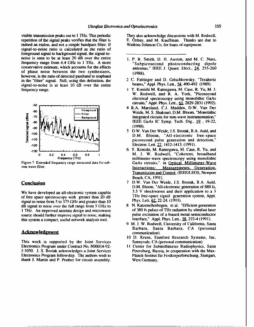
Ultrafast Electronics and Optoelectronics 115
visible transmission peaks out to I THz. This periodic They also acknowledge discussions with M. Rodwell,repetition of the signal peaks verifies that the filter is E. Ozbay, and M. Kauffman. Thanks are due toindeed an etalon, and not a simple bandpass filter. If Watkins-Johnson Co. for loans of equipment.signal-to-noise ratio is calculated as the ratio offoreground signal to background signal, the signal-to-noise is seen to be at least 20 dB over the entire 1. P. R. Smith, D. H. Auston, and M. C. Nuss,frequency range from 6.4 GHz to I THz. A more "Subpicosecond photoconducting dipoleconservative estimate, which accounts for the effects antennas," IEEE J. Quant. Elect., 24, 255-260of phase noise between the two synthesizers, (1988).however, is the ratio of detected passband to stopbandin the "filter" signal. Still, using this definition, the 2 C. Fattinger and D. Grischkowsky, "Terahertzsignal-to-noise is at least 10 dB over the entire beams," Appi. Phys. Lett., 5A, 490-492 (1989).frequency range. 3 Y. Konishi M. Kamegawa. M. Case, R. Yu, M. J.
W. Rodwell, and R. A. York, "Picosecondelectrical spectroscopy using monolithic GaAs
circuits," Appl. Phys. Lett., 61, 2829-2831 (1992).-oF n 4 R.A. Marsland, C.J. Madden, D.W. Van DerFoeg•rt•r, Weide, M. S. Shakouri, D.M. Bloom, "Monolithic
-70 ' L , --. Background integrated circuits for mm-wave instrumentation,"-80 IEEE GaAs IC Symp. Tech. Dig., 19., 19-22,
-90 (1990).5 D.W. Van Der Weide, J.S. Bostak, B.A. Auld, and
-100 D.M. Bloom, "All-electronic free-space-110 .. ... picosecond pulse generation and detection,"-120 Electron. Lett. 27, 1412-1413, (1991).-130 -- - ---- 6 Y. Konishi, M. Kamegawa, M. Case, R. Yu, and
0 0.2 0.4 0.6 0.8 1 M. J. W. Rodwell, "Coherent, broadbandFrequency (THz) millimeter-wave spectroscopy using monolithic
Figure 7 Extended frequency range measured data for sub- GaAs circuits,", in Optical Millimeter-Wavemm wave filter. Interactions: Measurements. Generation.
Transmission and Control (IEEE/LEOS, NewportBeach, CA, 1991).
u 7 D.W. Van Der Weide, J.S. Bostak, B.A. Auld,D.M. Bloom, "All-electronic generation of 880 fs,
We have developed an all-electronic system capable 3.5 V shockwaves and their application to a 3of free space spectroscopy with greater than 20 dB THz free-space signal generation system, Appl.signal to noise from 5 to 375 GHz and greater than 10 Phys. Lett. Q2. 22-24, (1993).dB signal to noise over the full range from 5 GHz to 8 N. Katzenellenbogen, et al. "Efficient generationI THz. An improved antenna design and microwave of 380 fs pulses of THz radiation by ultrafast lasersource should further improve signal to noise, making pulse excitation of a biased metal-semiconductorthis system a compact, useful network analysis tool. interface," Appi. Phys. Lett., 58, 222-4 (1991).
9 M. J. W. Rodwell, University of California, SantaBarbara, Santa Barbara, CA (personal
Acknowledgment communication).10 D. Kruse, Stanford Research Systems, Inc.
This work is supported by the Joint Services Sunnyvale, CA (personal communication).Electronics Program under Contract No. N00014-92- I I Center for Submillimeter Radiophysics, SaintJ-1050. J. S. Bostak acknowledges a Joint Services Petersburg, Russia, in cooperation with the Max-Electronics Program fellowship. The authors wish to Planck-Institut ffir Festkorperforschung, Stuttgart,thank J. Martin and P. Prather for circuit assembly. West Germany.
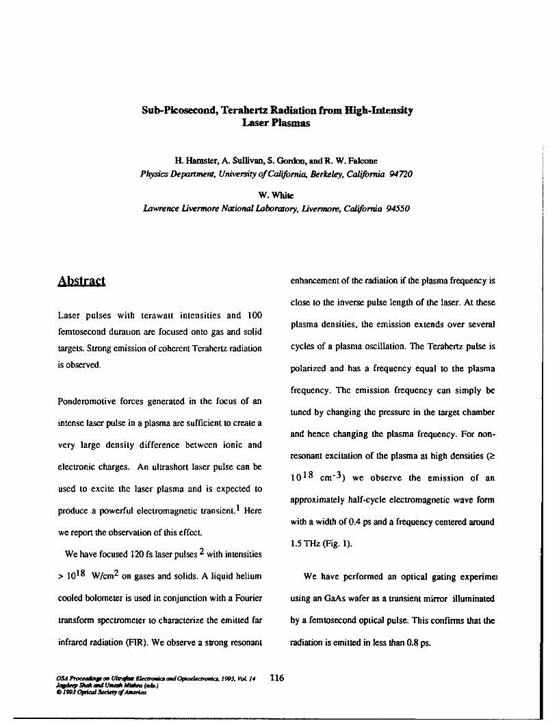
Sub-Picosecond, Terahertz Radiation from High-IntensityLaser Plasmas
H. Hamster, A. Sullivan, S. Gordon, and R. W. Falcone
Physics Department, University of California, Berkeley, California 94720
W. WhiteLawrence Livermore National Laboratory, Livermore, California 94550
Abstract enhancement of the radiation if the plasma frequency is
close to the inverse pulse length of the laser. At theseLaser pulses with terawatt intensities and 100
femntosecond duration are focused onto gas and solid plasma densities, the emission extends over several
targets. Strong emission of coherent Terahertz radiation cycles of a plasma oscillation. The Terahertz pulse is
is observed, polarized and has a frequency equal to the plasma
frequency. The emission frequency can simply bePonderomotive forces generated in the focus of an
tuned by changing the pressure in the target chamberintense laser pulse in a plasma are sufficient to create a
and hence changing the plasma frequency. For non-very large density difference between ionic and
resonant excitation of the plasma at high densities (>electronic charges. An ultrashort laser pulse can be 1018 cm" 3 ) we observe the emission of an
used to excite the laser plasma and is expected toapproximately half-cycle electromagnetic wave form
produce a powerful electromagnetic transient.1 Here
with a width of 0.4 ps and a frequency centered aroundwe report the observation of this effect.
1.5 THz (Fig. 1).
We have focused 120 fs laser pulses 2 with intensities
> 1018 W/cm 2 on gases and solids. A liquid helium We have performed an optical gating experimei
cooled bolometer is used in conjunction with a Fourier using an GaAs wafer as a transient mirror illuminated
transform spectrometer to characterize the emitted far by a femtosecond optical pulse. This confirms that the
infrared radiation (FIR). We observe a strong resonant radiation is emitted in less than 0.8 ps.
OSA PNocaae~g an Ukr*N Ela andOptoekaroxiex 1993, VoL 14 116tapk Suds amd tmed, Midenz (e&k)
o 1993 Opitcal Sodu~y qfAuateaz
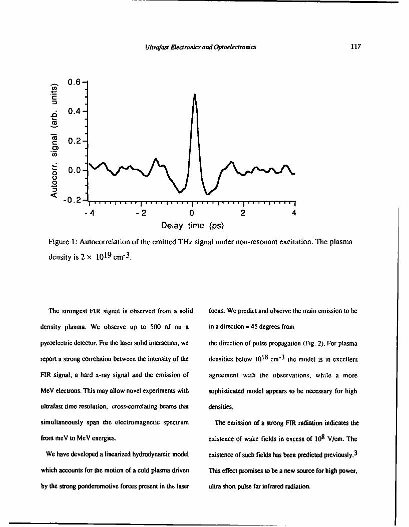
Ultrafast Electronics and Optoelectronics 117
0.6
C
S0.4
e 0.2
0 0.00 -0
-0.2 L4.
-4 -2 0 2 4
Delay time (ps)
Figure 1: Autocorrelation of the emitted THz signal under non-resonant excitation. The plasma
density is 2 x 1019 cm- 3 .
The strongest FIR signal is observed from a solid focus. We predict and observe the main emission to be
density plasma. We observe up to 500 nJ on a in a direction -45 degrees from
pyroelectric detector. For the laser solid interaction, we the direction of pulse propagation (Fig. 2). For plasma
report a strong correlation between the intensity of the densities below 1018 cm"3 the model is in excellent
FIR signal, a hard x-ray signal and the emission of agreement with the observations, while a more
MeV electrons. This may allow novel experiments with sophisticated model appears to be necessary for high
ultrafast time resolution, cross-correlating beams that densities.
simultaneously span the electromagnetic spectrum The emission of a strong FIR radiation indicates the
from meV to MeV energies. existence of wakc fields in excess of 108 V/cm. The
We have developed a linearized hydrodynamic model existence of such fields has been predicted previously. 3
which accounts for the motion of a cold plasma driven This effect promises to be a new source for high power,
by the strong ponderomotive forces present in the laser ultra short pulse far infrared radiation.
118 Ukrafast Electronics and Optoe/ectronics
1.5 -Angle (rad)
Pover(W/sr)
0
0.2
Time (ps)-O.22
Figure 2: Calculated radiation pattern.
The vertical axis denotes intensity, the bottom axis is time (ps) and the right hand axis is the viewangle in degrees from the beam propagation direction. The data is calculated for a plasma densityof 2 x 1019 cm-3 . The pulse length is 0.15 p,, the pulse energy is 20 mJ and the beam diameter 4g.m.
REEERENCES 2. A. Sullivan, H. Hamster, H.C. Kapteyn, S. Gordon,
W. White, H. Nathel, R.J. Blair, R.W. Falcone, Opt.
1. H. Hamster, R.W. Falcone, in Ultrafast Phenomena Leu. 16, 1406 (1991).
VII, C.B. Harris, E.P. Ippen, G. A. Mourou, A. H. 3. P. Sprangle, E. Esarey, A. Ting, Phys. Rev. Lett.
Zewail, eds. (Springe~r-Verlag, Berlin, 1990) pp. 122- 64, 2011 (1990); S. Wilks, W. Kruer, M. Tabak, A.
124. Langdon : Phys. Rev. Lett. 69, 1383 (1992).
Intense THz Beam from Organic Electro-Optic Materials
X. -C. Zhang and T. -M. LuPhysics Department, Rensselaer Polyechnic Institute, Troy, New York 12180-3590
C. P. Yakymyshyn
General Electric Research and Development Center, I River Road Schenectady, New York 12301
Abstract orientation). In this crystalline form thechromophores align in a herringbone motif
We report THz optical rectification from with a 200 half-angle from theorganic electro-optic crystals. The magnitude crystallographic a axis, resulting in a well-of the rectified field from an organic salt is aligned polar molecular packing. Powderone and two orders larger than that from GaAs second harmonic generation efficiency 1000and LiTaO3, respectively, times that of an Urea reference standard at a
fundamental wavelength of 1.9 grm wasIntroduction reported. Electro-optic measurements at 820
nm resulted in a Pockels coefficient of r 11 >In recent years different photonic and 400 pm/V [7,8] and Maker fringeoptoelectronic techniques have been used to measurements at 1.905 gin provided d1l = 600generate THz bandwidth free space radiation + 100 pm/V. Crystals of DAST were grown by[1-5]. Optical rectification is one technique slow evaporation of saturated methanolused for generating subpicosecond solutions. Crystal plates as large as 6 x 8 x 1.5submillimeter-wave radiation [6]. Developing mm with shiny facets and dark red color innew radiation sources will have a substantial transmitted light were grown from solutionimpact on high-speed, broadband over several weeks. Typical DAST samplescharacterization of dielectric materials. We used were 4 x 5 mm with thicknesses varyingextend previous work on generating free space from 0.2 to 1.7 mm.pulsed THz radiation, and report the The experimental setup is a coherent laserobservations of efficient optical rectification beam and THz beam pump-probeand sub-millimeter wave generation by an arrangement and has been describedorganic electro-optic crystal. elsewhere [6]. A cw Ar laser pumped, mode-
locked Ti:sapphire laser (Coherent MIRA)Experiment was used as the source of optical pulses. A 50
Twm photoconducting antenna was used as theThe organic crystal we used is Dimethyl detector.
Amino 4-N-Methylstilbazolium Tosylate
(DAST), which is a member of theStilbazolium salt family [7]. Fig. 1 shows the temporal waveform of the
radiated field from a 0.4 mm thick DASTsample. The largest radiated signal detected
Under appropriate conditions, DAST by a 50 micron photoconducting antennacrystallizes in the acentric monoclinic Cc (time-averaged) was 9.8 mV, corresponding tospace group, point group m (standard an electric field of nearly 2 V/cm. A persistent
osA Neap w d Optoelecrtm 1993. Vol. 14 119Jq0d 9t. td LUmnes Mlaa (atk)0 1993 pdcal So&dcy cAmra
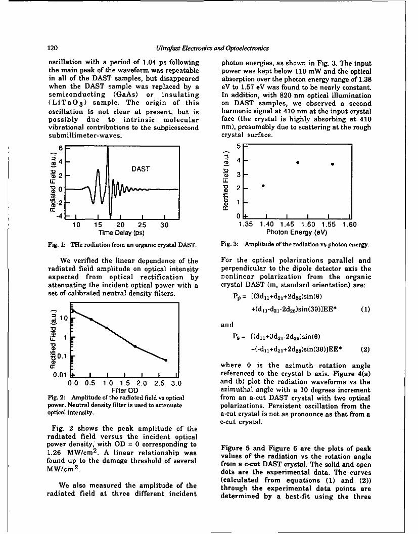
120 Ultrafast Electronics and Oproelectronics
oscillation with a period of 1.04 ps following photon energies, as shown in Fig. 3. The inputthe main peak of the waveform was repeatable power was kept below 110 mW and the opticalin all of the DAST samples, but disappeared absorption over the photon energy range of 1.38when the DAST sample was replaced by a eV to 1.57 eV was found to be nearly constant.semiconducting (GaAs) or insulating In addition, with 820 nm optical illumination(LiTaO 3 ) sample. The origin of this on DAST samples, we observed a secondoscillation is not clear at present, but is harmonic signal at 410 nm at the input crystalpossibly due to intrinsic molecular face (the crystal is highly absorbing at 410vibrational contributions to the subpicosecond nm), presumably due to scattering at the roughsubmillimeter-waves. crystal surface.
6 5
DASTIL
-4 010 15 20 25 30 1.35 1.40 1.45 1.50 1.55 1.60
Time Delay (ps) Photon Energy (eV)
Fig. 1: THz radiation from an organic crystal DAST. Fig. 3: Amplitude of the radiation vs photon energy.
We verified the linear dependence of the For the optical polarizations parallel andradiated field amplitude on optical intensity perpendicular to the dipole detector axis theexpected from optical rectification by nonlinear polarization from the organicattenuating the incident optical power with a crystal DAST (m, standard orientation) are:set of calibrated neutral density filters. Pp= [(3d1 1 +d 2 1+2d 26 )sin(0)
+(d, l-d 2 -2d 26 )sin(30)]EE* (1)
10 and
S1 Ps = [(djj+3d 21 -2d 26 )sin(O)
+(-dl I+d 2i+2d2s)sin(30)]EE* (2)
0X where 0 is the azimuth rotation angle
0.01 referenced to the crystal b axis. Figure 4(a)0.0 0.5 1.0 1.5 2.0 2.5 3.0 and (b) plot the radiation waveforms vs the
Filter OD azimuthal angle with a 10 degrees incrementFig. 2: Amplitude of the radiated field vs optical from an a-cut DAST crystal with two opticalpower. Neutral density filter is used to attenuate polarizations. Persistent oscillation from theoptical intensity, a-cut crystal is not as pronounce as that from a
c-cut crystal.Fig. 2 shows the peak amplitude of the
radiated field versus the incident opticalpower density, with OD = 0 corresponding to Figure 5 and Figure 6 are the plots of peak1.26 MW/cm 2 . A linear relationship was values of the radiation vs the rotation anglefound up to the damage threshold of several from a c-cut DAST crystal. The solid and openMW/cm 2 . dots are the experimental data. The curves
(calculated from equations (1) and (2))We also measured the amplitude of the through the experimental data points are
radiated field at three different incident determined by a best-fit using the three
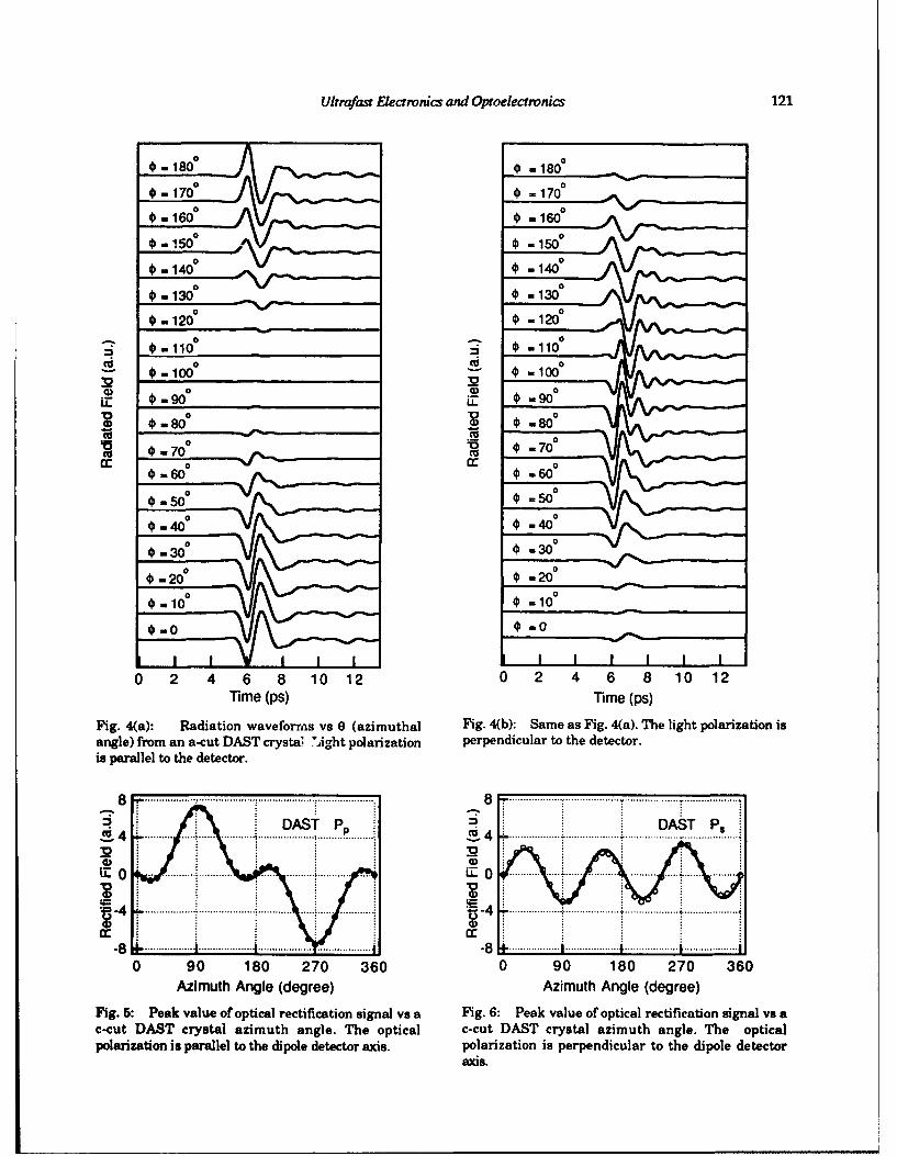
Ultrafast Electronics and Optoelectronics 121
0 - 180° ,* - 180°
S" 140 0 0 -14
0.130 . 'i- " 130)- 120 0 -- - 120° *
0 0
" " ,0.-110° " 0 - 110° j•
41 - 8.*oR -0 _,80
0 26 4 6 1 1 0 2 4 660101
8.........................
.54 501 0 = 50°$ .40°0 0••'' .400
S- 30° 0 N - 300
-200= 200
000
0 . -0
0 2 4 6 8 10 12 0 2 4 6 8 10 12Time (ps) Time (ps)
Fig. 4(a): Radiation waveforpc s vs 0 (azimuthal Fig. 4(b): Same as Fig. 4(a). The light polarization isangle) from an a-cut DAST crystal light polarization perpendicular to the detector.is parallel to the detector.
"D T P"ax DAST Ps
i :: 0 .. ..... ... .. ... .*.................... . .. .. . .. .............. .. . . .. I . . ........... . .
0 90 180 270 360 0 90 180 270 360
Azimuth Angle (degree) Azimuth Angle (degree)
Fig. 5: Peak value of optical rectification signal vs a Fig. 6: Peak value of optical rectification signal ve ac-cut DAST crystal azimuth angle. The optical c-cut DAST crystal azimuth angle. The opticalpolarization is parallel to the dipole detector axis. polarization is perpendicular to the dipole detector
axis.
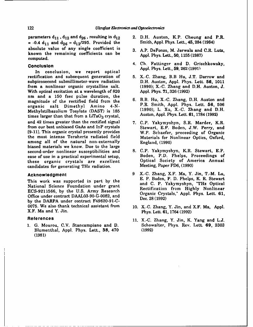
122 Ultrafost Elecarorucs and Optoelectronics
parameters d1l , d1 2 and d2 6 , resulting in d1 2 2. D.H. Auston, K.P. Cheung and P.R.
= -0.4 d1l and d2 6 = d 1 2 /295. Provided the Smith, Appl. Phys. Lett., 45, 284 (1984)
absolute value of any single coefficient is 3. A.P. DeFonzo, M. Jarwala and C.R. Lutz,known the remaining coefficients can be Appl. Phys. Lett., 50, 1155(1987)computed.
Conclusion 4. Ch. Fattinger and D. Grischkowsky,
In conclusion, we report optical Appl. Phys. Lett., 59, 262 (19911
rectification and subsequent generation of 5. X.-C. Zhang, B.B Hu, J.T. Darrow andsubpicosecond submillimeter-wave radiation D.H. Auston, Appl. Phys. Lett. 56, 1011from a nonlinear organic crystalline salt. (1990); X.-C. Zhang and D.H. Auston, J.With optical excitation at a wavelength of 820 Appl. Phys. 71, 326 (1992)nm and a 150 fsec pulse duration, themagnitude of the rectified field from the 6. B.B. Hu, X.-C. Zhang, D.H. Auston andorganic salt Dimethyl Amino 4-N- P.R. Smith, Appl. Phys. Lett. 56, 506Methylstilbazolium Tosylate (DAST) is 185 (1990); L. Xu, X.-C. Zhang and D.H.
times larger than that from a LiTaO3 crystal, Auston, Appl. Phys. Lett. 61, 1784 (1992)
and 42 times greater than the rectified signal 7. C.P. Yakymyshyn, S.R. Marder, K.R.from our best unbiased GaAs and InP crystals Stewart, E.P. Boden, J.W. Perry, and[9-11]. This organic crystal presently provides W.P. Schaefer, preceeding of Organicthe most intense Terahertz radiated field Materials for Nonlinear Optics, Oxford,among all of the natural non-externally England, (1990)biased materials we know. Due to the largesecond-order nonlinear susceptibilities and 8. C.P. Yakymyshyn, K.R. Stewart, E.P.ease of use in a practical experimental setup, Boden, P.D. Phelps, Proceedings of
these organic crystals are excellent Optical Society of America Annual
candidates for generating THz radiation. Meeting, Paper FD6, (1990)
Acknowledgment 9 X.-C. Zhang, X.F. Ma, Y. Jin, T.-M. Lu,This work was supported in part by the E. P. Boden, P. D. Phelps, K R. Stewart
National Science Foundation under grant and C. P. Yakymyshyn, "THz Optical
ECS-9211566, by the U.S. Army Research Rectification from Highly Nonlinear
Office under contract'DAAL03-90-G-0082, and Organic Crystals," Appl. Phys. Lett. 61,
by the DARPA under contract F49620-91-C-
0075. We also thank technical assistant from 10. X.-C. Zhang, Y. Jin, and X.F. Ma, Appl.X.F. Ma and Y. Jin. Phys. Lett. 61, 1764 (1992)
References 11. X.-C. Zhang, Y. Jin, K. Yang and L.J.
1. G. Mourou, C.V. Stancampiano and D. Schowalter, Phys. Rev. Lett. 69, 2303Blumenthal, Appl. Phys. Lett., 38, 470 (1992)(1981)
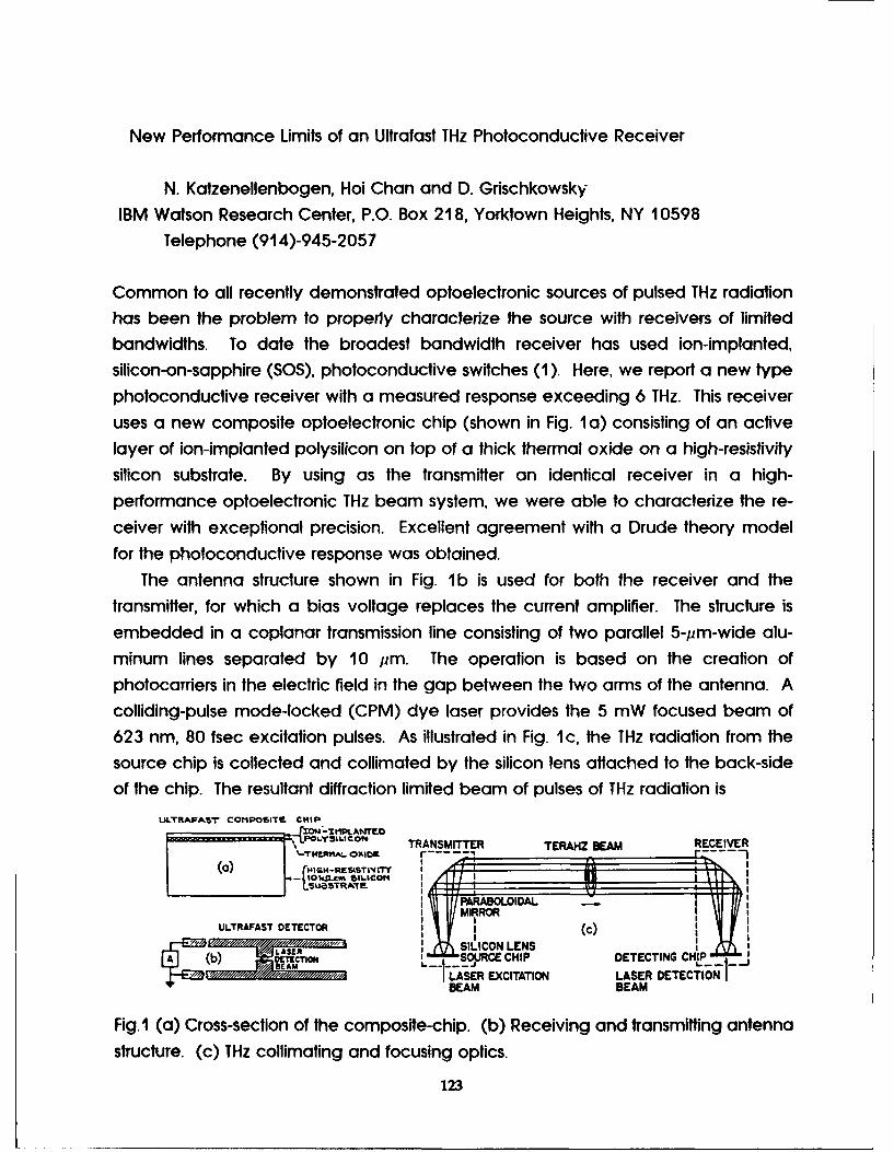
New Performance Limits of an Ultrafast THz Photoconductive Receiver
N. Katzenellenbogen, Hoi Chan and D. Grischkowsky
IBM Watson Research Center, P.O. Box 218, Yorktown Heights, NY 10598
Telephone (914)-945-2057
Common to all recently demonstrated optoelectronic sources of pulsed THz radiation
has been the problem to property characterize the source with receivers of limited
bandwidths. To date the broadest bandwidth receiver has used ion-implanted,
silicon-on-sapphire (SOS), photoconductive switches (1). Here, we report a new type
photoconductive receiver with a measured response exceeding 6 THz. This receiver
uses a new composite optoelectronic chip (shown in Fig. 1a) consisting of an active
layer of ion-implanted polysilicon on top of a thick thermal oxide on a high-resistivity
silicon substrate. By using as the transmitter an identical receiver in a high-
performance optoelectronic THz beam system, we were able to characterize the re-
ceiver with exceptional precision. Excellent agreement with a Drude theory model
for the photoconductive response was obtained.
The antenna structure shown in Fig. lb is used for both the receiver and the
transmitter, for which a bias voltage replaces the current amplifier. The structure is
embedded in a coplanar transmission line consisting of two parallel 5-pm-wide alu-
minum lines separated by 10 pm. The operation is based on the creation of
photocarriers in the electric field in the gap between the two arms of the antenna. A
colliding-pulse mode-locked (CPM) dye laser provides the 5 mW focused beam of
623 nm, 80 fsec excitation pulses. As illustrated in Fig. Ic, the THz radiation from the
source chip is collected and collimated by the silicon lens attached to the back-side
of the chip. The resultant diffraction limited beam of pulses of THz radiation is
ULTRAFAST COMtPOSITE CH4tIJ'zoW-X PLAt.MT.O
•-.~ .OLYSIIC TRANSMITTER TERAHZ BEAM RECEIVERr-n I ..i.o _...._--
SUBSTRAIM "
I MILRROR CMIULTRAFAST ODTECTOR I (c)SILICON LENS
_jRECHIP DETECTING CI
-4LASER EXCITATION LASER DETECTIONBEAM BEAM
Fig. 1 (a) Cross-section of the composite-chip. (b) Receiving and transmitting antenna
structure. (c) THz collimating and focusing optics.
123
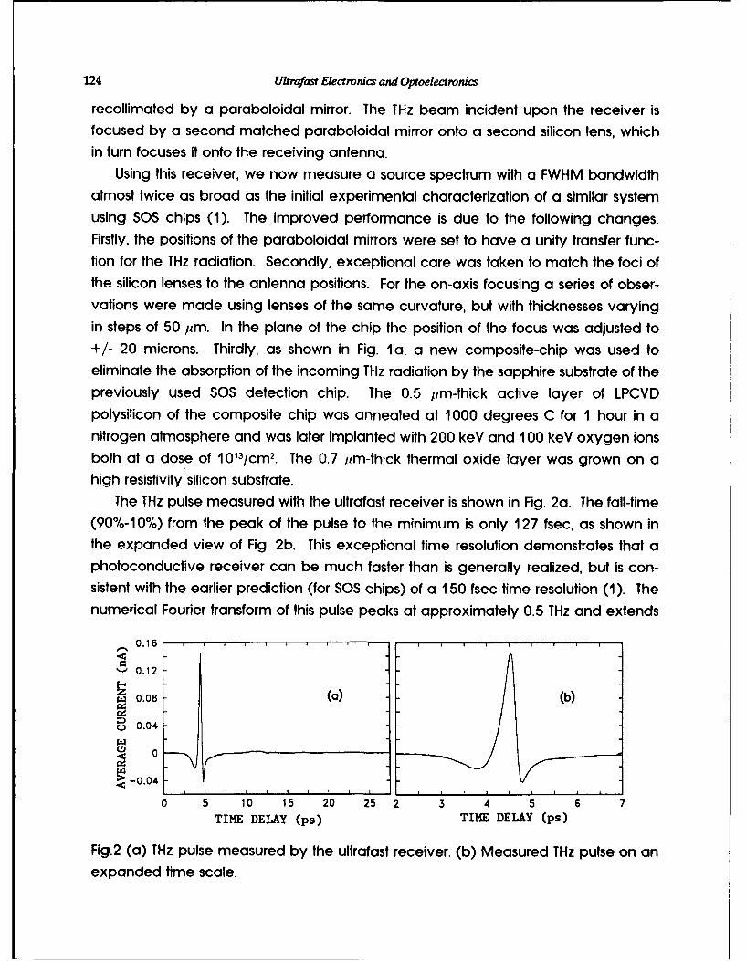
124 Ufrrafast Electronics and Optoelectronics
recollimated by a paraboloidal mirror. The THz beam incident upon the receiver isfocused by a second matched paraboloidal mirror onto a second silicon lens, whichin turn focuses it onto the receiving antenna.
Using this receiver, we now measure a source spectrum with a FWHM bandwidthalmost twice as broad as the initial experimental characterization of a similar systemusing SOS chips (1). The improved performance is due to the following changes.Firstly, the positions of the paraboloidal mirrors were set to have a unity transfer func-
tion for the THz radiation. Secondly, exceptional care was taken to match the foci ofthe silicon lenses to the antenna positions. For the on-axis focusing a series of obser-vations were made using lenses of the same curvature, but with thicknesses varying
in steps of 50 pm. In the plane of the chip the position of the focus was adjusted to+1- 20 microns. Thirdly, as shown in Fig. l a, a new composite-chip was used toeliminate the absorption of the incoming THz radiation by the sapphire substrate of the
previously used SOS detection chip. The 0.5 pm-thick active layer of LPCVDpolysilicon of the composite chip was annealed at 1000 degrees C for 1 hour in anitrogen atmosphere and was later implanted with 200 keV and 100 keV oxygen ionsboth at a dose of I0 13/cm 2 . The 0.7 jim-thick thermal oxide layer was grown on a
high resistivity silicon substrate.The THz pulse measured with the ultrafast receiver is shown in Fig. 2a. The fall-time
(90%-10%) from the peak of the pulse to the minimum is only 127 fsec, as shown inthe expanded view of Fig. 2b. This exceptional time resolution demonstrates that a
photoconductive receiver can be much faster than is generally realized, but is con-sistent with the earlier prediction (for SOS chips) of a 150 fsec time resolution (1). The
numerical Fourier transform of this pulse peaks at approximately 0.5 THz and extends
0.16 .....
S0.12
0.08 (a) (b)
c=) 0.04
0
! -0.04 .
0 5 10 15 20 25 2 , 4 5 6 7
TIME DELAY (ps) TIME DELAY (ps)
Fig.2 (a) THz pulse measured by the ultrafast receiver. (b) Measured THz pulse on an
expanded time scale.
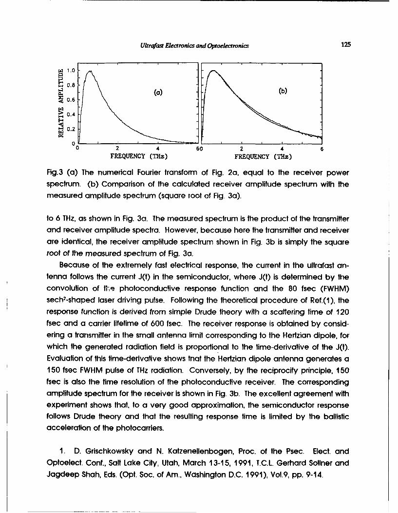
Ulrraast Electronics and Opoelectronics 125
g 1.0
S0.8S(a) (b)
44 0.6
~0.4
•0.2
0 ' ---- -0 2 4 60 2 4 6
FREQUENCY (THz) FREQUENCY (THz)
Fig.3 (a) The numerical Fourier transform of Fig. 2a, equal to the receiver powerspectrum. (b) Comparison of the calculated receiver amplitude spectrum with themeasured amplitude spectrum (square root of Fig. 3a).
to 6 THz, as shown in Fig. 3a. The measured spectrum is the product of the transmitterand receiver amplitude spectra. However, because here the transmitter and receiverare identical, the receiver amplitude spectrum shown in Fig. 3b is simply the square
root of the measured spectrum of Fig. 3a.Because of the extremely fast electrical response, the current in the ultrafast an-
tenna follows the current J(t) in the semiconductor, where J(t) is determined by theconvolution of t[,e photoconductive response function and the 80 fsec (FWHM)sech2-shaped laser driving pulse. Following the theoretical procedure of Ref.(1), the
response function is derived from simple Drude theory with a scatlering time of 120fsec and a carrier lifetime of 600 fsec. The receiver response is obtained by consid-ering a transmitter in the small antenna limit corresponding to the Hertzian dipole, for
which the generated radiation field is proportional to the time-derivative of the J(t).Evaluation of this time-derivative shows tnat the Hertzian dipole antenna generates a150 fsec FWHM pulse of THz radiation. Conversely, by the reciprocity principle, 150fsec is also the time resolution of the photoconductive receiver. The correspondingamplitude spectrum for the receiver is shown in Fig. 3b. The excellent agreement withexperiment shows that, to a very good approximation, the semiconductor responsefollows Drude theory and that the resulting response time is limited by the ballistic
acceleration of the photocarriers.
1. D. Grischkowsky and N. Katzenellenbogen, Proc. of the Psec. Elect. andOptoelect. Conf., Salt Lake City, Utah, March 13-15, 1991, T.C.L. Gerhard Sollner andJagdeep Shah, Eds. (Opt. Soc. of Am., Washington D.C. 1991), Vol.9, pp. 9-14.
Physics of Semiconductors
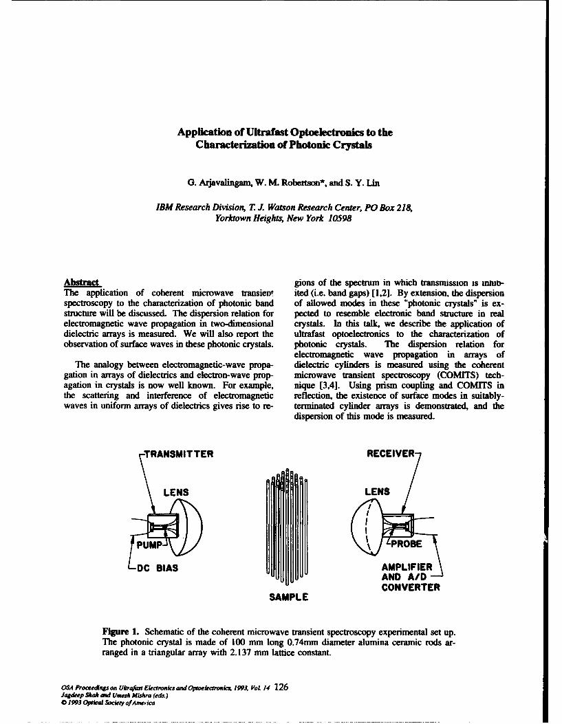
Application of Ultrafast Optoelectronics to theCharacterization of Photonic Crystals
G. Arjavalingam, W. M. Robertson*, and S. Y. Lin
IBM Research Division, T. J. Watson Research Center, PO Box 218,Yorktown Heights, New York 10598
Abstrmt gions of the spectrum in which transmission is mrni-The application of coherent microwave transient ited (i.e. band gaps) [1,2]. By extension, the dispersionspectroscopy to the characterization of photonic band of allowed modes in these "photonic crystals" is ex-structure will be discussed. The dispersion relation for pected to resemble electronic band structure in realelectromagnetic wave propagation in two-dimensional crystals. In this talk, we describe the application ofdielectric arrays is measured. We will also report the ultrafast optoelectronics to the characterization ofobservation of surface waves in these photonic crystals. photonic crystals. The dispersion relation for
electromagnetic wave propagation in arrays ofThe analogy between electromagnetic-wave propa- dielectric cylinders is measured using the coherent
gation in arrays of dielectrics and electron-wave prop- microwave transient spectroscopy (COM1TS) tech-agation in crystals is now well known. For example, nique [3,4]. Using prism coupling and COMMTS inthe scattering and interference of electromagnetic reflection, the existence of surface modes in suitably-waves in uniform arrays of dielectrics gives rise to re- terminated cylinder arrays is demonstrated, and the
dispersion of this mode is measured.
TRANSMIT TER RECEIVER
LENS LENS
I
PUMP PROBE
DC BIAS AMPLIF IER-Uuu AND A/D
CONVERTERSAMPLE
Figure 1. Schematic of the coherent microwave transient spectroscopy experimental set up.The photonic crystal is made of 100 mm long 0.74mm diameter alumina ceramic rods ar-ranged in a triangular array with 2.137 mm lattice constant.
osA Proceednps on Ubrafau Electronics and Optoekctronics 1i93. VoL 14 126Jagdeep Shah and Unesh Mishra (eds.)0 1993 Optical Sociery ofAmerica
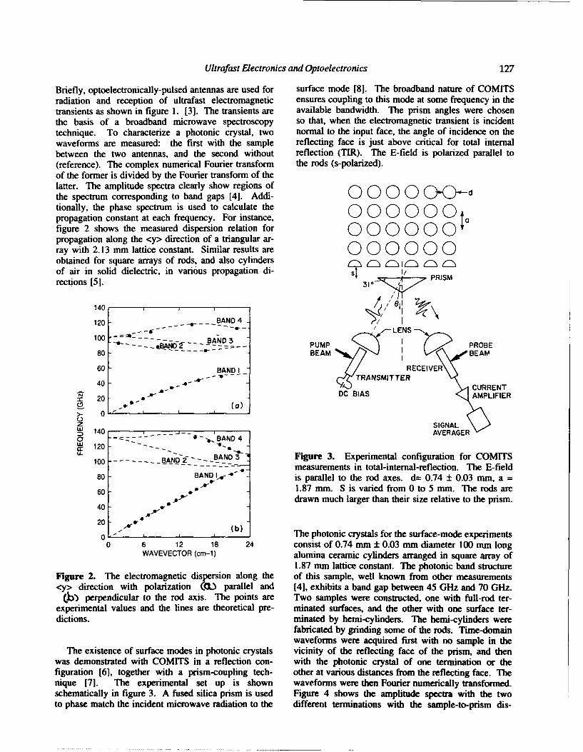
Ultrafast Electronics and Optoelectronics 127
Briefly, optoelectronically-pulsed antennas are used for surface mode [8]. The broadband nature of COMITSradiation and reception of ultrafast electromagnetic ensures coupling to this mode at some frequency in thetransients as shown in figure 1. [3]. The transients are available bandwidth. The prism angles were chosenthe basis of a broadband microwave spectroscopy so that, when the electromagnetic transient is incidenttechnique. To characterize a photonic crystal, two normal to the input face, the angle of incidence on thewaveforms are measured: the first with the sample reflecting face is just above critical for total internalbetween the two antennas, and the second without reflection (TIR). The E-field is polarized parallel to(reference). The complex numerical Fourier transform the rods (s-polarized).of the former is divided by the Fourier transform of thelatter. The amplitude spectra clearly show regions of ) C 0 C dthe spectrum corresponding to band gaps [4]. Addi-tionally, the phase spectrum is used to calculate thepropagation constant at each frequency. For instance, 0figure 2 shows the measured dispersion relation for 0 0 0 0 0 0propagation along the <y> direction of a triangular ar-ray with 2.13 mm lattice constant. Similar results are C C) C)0obtained for square arrays of rods, and also cylinders - CLof air in solid dielectric, in various propagation di- ISrections [5]. 31o PRISM7
140
120 BAND4-- 0 L ENS LENS
100 = :=.... .... BAND 310 --.....BAND2 B- -- PUMP PROBE
80 - BEAM BEAM
60 BAND I RECEIVER4 ---- TRANSMITTER B
A CURRENT*- " DC BIAS AMPLIFIER: 20 -
S,,.,-(a)4-0
% ,>..0
z SIGNALu' 140 AVERAGERo - .. BAND 4c 120 - .
100 --------- BAND 2 -BAND 3 Figure 3. Experimental configuration for COMITSmeasurements in total-internal-reflection. The E-field
80 BAND I1"- is parallel to the rod axes. d= 0.74 ± 0.03 mm, a =
60 " 1.87 mm. S is varied from 0 to 5 mm. The rods are40* ,.-" drawn much larger than their size relative to the prism.40 - m.e
20 ,*e- (b)
0 - I- 2 4The photonic crystals for the surface-mode experiments0 6 12 18 24 consist of 0.74 mm ± 0.03 mm diameter 100 mnm long
WAVEVECTOR (cm-1) alumina ceramic cylinders arranged in square array of1.87 mm lattice constant. The photonic band structure
Figure 2. The electromagnetic dispersion along the of this sample, well known from other measurements<y> direction with polarization (0W) parallel and [4], exhibits a band gap between 45 GHz and 70 GHz.
(1o) perpendicular to the rod axis. The points are Two samples were constructed, one with full-rod ter-experimental values and the lines are theoretical pre- minated surfaces, and the other with one surface ter-dictions. minated by hemi-cylinders. The hemi-cylinders were
fabricated by grinding some of the rods. Time-domainwaveforms were acquired first with no sample in the
The existence of surface modes in photonic crystals vicinity of the reflecting face of the prism, and thenwas demonstrated with COMITS in a reflection con- with the photonic crystal of one termination or thefiguration [61, together with a prism-coupling tech- other at various distances from the reflecting face. Thenique [7]. The experimental set up is shown waveforms were then Fourier numerically transformed.schematically in figure 3. A fused silica prism is used Figure 4 shows the amplitude spectra with the twoto phase match the incident microwave radiation to the different terminations with the sample-to-prism dis-
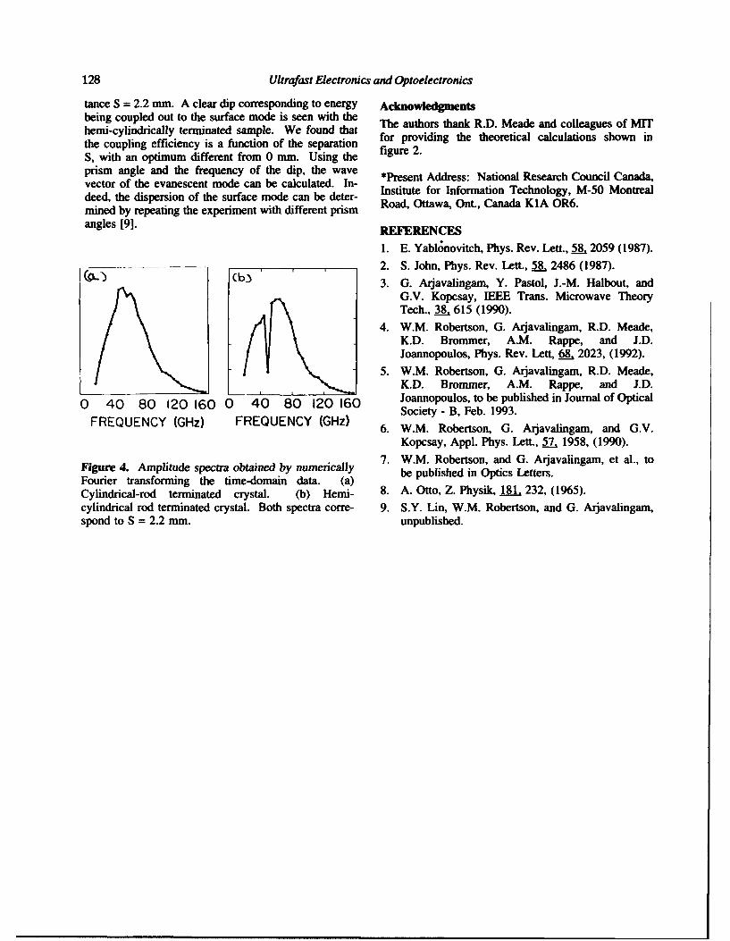
128 Ultrafast Electronics and Optoelectronics
tance S = 2.2 mm. A clear dip corresponding to energy Acknowledgmentsbeing coupled out to the surface mode is seen with thehemi-cylindrically terminated sample. We found that The authors thank R.D. Meade and colleagues of MITthe coupling efficiency is a function of the separation for providing the theoretical calculations shown inS, with an optimum different from 0 mm. Using the fig 2.prism angle and the frequency of the dip, the wavevector of the evanescent mode can be calculated. In- *Isent Address: National Research Council Canada,deed, the dispersion of the surface mode can be deter- Institute for Information Technology, M-50 Montrealmined by repeating the experiment with different prism Road, Ottawa, Ont., Canada KIA OR6.angles [9]. REFERENCES
1. E. Yablonovitch, Phys. Rev. Lett., 58. 2059 (1987).
2. S. John, Phys. Rev. Lett., 58, 2486 (1987)..(b) 3. G. Aijavalingam, Y. Pastol, J.-M. Halbout, and
G.V. Kopcsay, IEEE Trans. Microwave TheoryTech., 38, 615 (1990).
4. W.M. Robertson, G. Aijavalingam, R.D. Meade,K.D. Brommer, A.M. Rappe, and J.D.Joannopoulos, Phys. Rev. Lett, 68, 2023, (1992).
5. W.M. Robertson, G. Arjavalingam, R.D. Meade,K.D. Brommer, A.M. Rappe, and J.D.
0 40 80 120 160 0 4•0 80 120 160 Joannopoulos, to be published in Journal of OpticalF 40z F Q N (G2z) 160 0 40 80120160 Society - B, Feb. 1993.FREQUENCY (GHz) FREQUENCY (GHz) 6. W.M. Robertson, G. Arjavalingam, and G.V.
Kopcsay, Appl. Phys. Lett., 57. 1958, (1990).7. W.M. Robertson, and G. Arjavalingam, et al., toFigure 4. Amplitude spectra obtained by numerically be published in Optics Letters.
Fourier transforming the time-domain data. (a)
Cylindrical-rod terminated crystal. (b) Hemi- 8. A. Otto, Z. Physik, 181. 232, (1965).cylindrical rod terminated crystal. Both spectra corre- 9. S.Y. Lin, W.M. Robertson, and G. Arjavalingam,spond to S = 2.2 mm. unpublished.
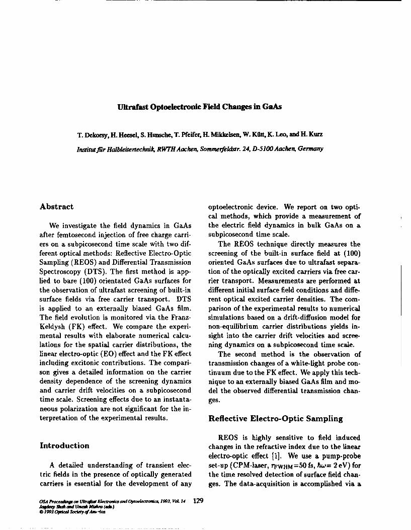
Ultrafast Optoelectronic Field Changes in GaAs
T. Dekorsy, H. Heesel, S. Hunsche, T. Pfeifer, H. likkelsen, W. Kilt, K. Leo, and IL Kurz
Instiutwfir Halbleitertechnik, RWTH Aachen, Sommerfeldstr. 24, D-5100 Aachen, Germany
Abstract optoelectronic device. We report on two opti-cal methods, which provide a measurement of
We investigate the field dynamics in GaAs the electric field dynamics in bulk GaAs on aafter femtosecond injection of free charge carri- subpicosecond time scale.ers on a subpicosecond time scale with two dif- The REOS technique directly measures theferent optical methods: Reflective Electro-Optic screening of the built-in surface field at (100)Sampling (REOS) and Differential Transmission oriented GaAs surfaces due to ultrafast separa-
Spectroscopy (DTS). The first method is app- tion of the optically excited carriers via free car-lied to bare (100) orientated GaAs surfaces for rier transport. Measurements are performed atthe observation of ultrafast screening of built-in different initial surface field conditions and diffe-surface fields via free carrier transport. DTS rent optical excited carrier densities. The com-is applied to an externally biased GaAs film. parison of the experimental results to numerical
The field evolution is monitored via the Franz- simulations based on a drift-diffusion model forKeldysh (FK) effect. We compare the experi- non-equilibrium carrier distributions yields in-mental results with elaborate numerical calcu- sight into the carrier drift velocities and scree-lations for the spatial carrier distributions, the ning dynamics on a subpicosecond time scale.
linear electro-optic (EO) effect and the FK effect The second method is the observation ofincluding excitonic contributions. The compari- transmission changes of a white-light probe con-son gives a detailed information on the carrier tinuum due to the FK effect. We apply this tech-
density dependence of the screening dynamics nique to an externally biased GaAs film and mo-and carrier drift velocities on a subpicosecond del the observed differential transmission chan-
time scale. Screening effects due to an instanta- ges.neous polarization are not significant for the in-terpretation of the experimental results. Reflective Electro-Optic Sampling
REOS is highly sensitive to field inducedIntroduction changes in the refractive index due to the linear
electro-optic effect [1]. We use a pump-probeA detailed understanding of transient elec- set-up (CPM-iaser, rFWHM= 5 0 fA, hW= 2 eV) for
tric fields in the presence of optically generated the time resolved detection of surface field chan-
carriers is essential for the development of any ges. The data-acquisition is accomplished via a
OSA ,Poa*nw pm Uln* Ekchwdes anudOproekcronicA 1993. VoL 14 129JAdaip Ma and Umtd MWra (da)o 1993 Op"ra Sm,*y tf• -ta
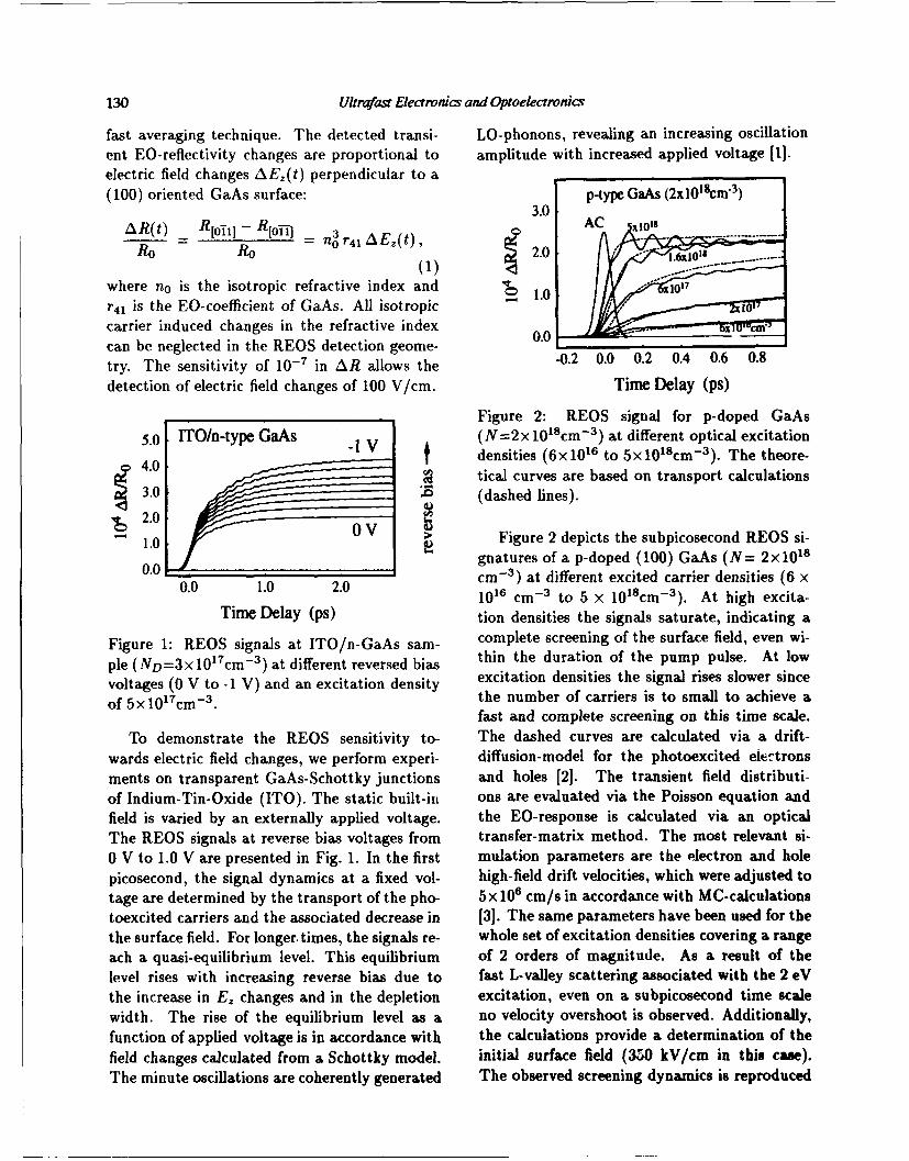
130 Ultrafas Electronics and Optoelectronics
fast averaging technique. The detected transi- LO-phonons, revealing an increasing oscillation
ent EO-reflectivity changes are proportional to amplitude with increased applied voltage [1].
electric field changes AE 2 (t) perpendicular to a(100) oriented GaAs surface: p-type GaAs (2x10 18cm- 3)
3.0AR(t) _ R[oT7] - R[O-1 _ =°3 AC 210" I - ---------
no f~l ~AlAE(t~),Ro Ro 2(1)
where no is the isotropic refractive index and 1.0 1017
r 41 is the EO-coefficient of GaAs. All isotropic / ,carrier induced changes in the refractive index 0 _can be neglected in the REOS detection geome-
try. The sensitivity of 10' in AR allows the -0.2 0.0 0.2 0.4 0.6 0.8
detection of electric field changes of 100 V/cm. Time Delay (ps)
Figure 2: REOS signal for p-doped GaAs
5.0 ITO/n-typeGaAs (N=2 x 10'8cm- 3 ) at different optical excitation
4.0 densities (6x 10¹⁶ to 5X10 18cm-3 ). The theore-tical curves are based on transport calculations
3.0 (dashed lines).
~2.0
1.0 - Figure 2 depicts the subpicosecond REOS si-
0.0 _ gnatures of a p-doped (100) GaAs (N= 2x10¹⁵
0.0 1cm- 3 ) at different excited carrier densities (6 x0.0 1.0 2.0 1016 cm-3 to 5 X 101Scm-3 ). At high excita-
Time Delay (ps) tion densities the signals saturate, indicating a
Figure 1: REOS signals at ITO/n-GaAs sam- complete screening of the surface field, even wi-
ple (ND=3x 101 7cm-3 ) at different reversed bias thin the duration of the pump pulse. At low
voltages (0 V to -1 V) and an excitation density excitation densities the signal rises slower since
of 5x 101 7 cm- 3 . the number of carriers is to small to achieve afast and complete screening on this time scale.
To demonstrate the REOS sensitivity to- The dashed curves are calculated via a drift-
wards electric field changes, we perform experi- diffusion-model for the photoexcited electrons
ments on transparent GaAs-Schottky junctions and holes [2]. The transient field distributi-
of Indium-Tin-Oxide (ITO). The static built-in ons are evaluated via the Poisson equation and
field is varied by an externally applied voltage, the EO-response is calculated via an optical
The REOS signals at reverse bias voltages from transfer-matrix method. The most relevant si-
0 V to 1.0 V are presented in Fig. 1. In the first mulation parameters are the electron and hole
picosecond, the signal dynamics at a fixed vol- high-field drift velocities, which were adjusted to
tage are determined by the transport of the pho- 5 x 106 cm/s in accordance with MC-calculationstoexcited carriers and the associated decrease in [3]. The same parameters have been used for the
the surface field. For longer, times, the signals re- whole set of excitation densities covering a range
ach a quasi-equilibrium level. This equilibrium of 2 orders of magnitude. As a result of the
level rises with increasing reverse bias due to fast L-valley scattering associated with the 2 eV
the increase in E. changes and in the depletion excitation, even on a subpicosecond time scale
width. The rise of the equilibrium level as a no velocity overshoot is observed. Additionally,
function of applied voltage is in accordance with the calculations provide a determination of the
field changes calculated from a Schottky model. initial surface field (350 kV/cm in this case).
The minute oscillations are coherently generated The observed screening dynamics is reproduced
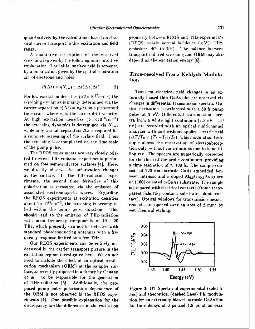
Ultrafast Electronics and Oproelectronics 131
quantitatively by the calculations based on clas- geometry between REOS and THz-experimen'ssical carrier transport in this excitation and field (REOS: nearly normal incidence (<50): THz-
range. emission: 400 to 700). The balance betweenA qualitative description of the observed transport-induced screening and ORM may also
screening is given by the following more intuitive depend on the excitation energy [6].explanation. The initial surface field is screenedby a polarization given by the spatial separation Time-resolved Franz-Keldysh Modula-Az of electrons and holes tion
P(At) = qNe,.(z, At)Az(At). (2)''Transient electrical field changes in an ex-
For low excitation densities (<5x 1017 cm- 3 ) the ternally biased thin GaAs film are observed viascreening dynamics is mainly determined via the changes in differential transmission spectra. Op-carrier separation z(At) = VdAt on a picosecond tical excitation is performed with a 50 fs pumptime scale, where Vd is the carrier drift velocity, pulse at 2 eV. Differential transmission spec-At high excitation densities (>lx10 18 cm- 3 ) tra from a white light continuum (1.3 eV - 1.9the screening dynamics is determined via Nxo, eV) are recorded with an optical multichannelwhile only a small separation Az is required for analyzer with and without applied electric fielda complete screening of the surface field. Thus (AT/To = (TE-To)/To). This modulation tech-the screening is accomplished on the time scale nique allows the observation of electroabsorp-of the pump pulse. tion only, without contributions due to band flu-
The REOS experiments are very closely rela- ling etc. The spectra are numerically correctedted to recent THz-emission experiments perfor- for the chirp of the probe continuum, providingmed on free semiconductor surfaces [4]. Here, a time resolution of ,z 100 fs. The sample con-we directly observe the polarization changes sists of 220 nm intrinsic GaAs embedded bet-at the surface. In the Tlfz-radiation expe- ween intrinsic and n-doped Al 0. 5Ga 0 5.ss grownriments, the second time derivative of this on (100) oriented n-GaAs substrate. The samplepolarization is measured via the emission of is prepared with electrical contacts (front: trans-associated electromagnetic waves. Regarding parent Schottky contact; substrate: ohmic con-the REOS experiments at excitation densities tact). Optical windows for transmission measu-about 2x 101 8 cm- 3 , the screening is accomplis- rements are opened over an area of 2 mm 2 byhed within the pump pulse duration. This wet chemical etching.should lead to the emission of THz-radiationwith main frequency components of 10 - 20THz, which presently can not be detected with 0.06standard photoconducting antennas with a fre- 0.04-&=OP0quency response limited to a few THz. t
Our REOS experiments can be entirely un- 0.02 A= i.psderstood in the carrier transport picture in theexcitation regime investigated here. We do not t 0.00
need to include the effect of an optical rectifi- -0.02cation mechanism (ORM) at the samples sur-face, as recently proposed in a theory by Chuang 1.35 1.40 1.45 1.50 1.55
et al. to be responsible for the generation Energy (eV)of THz-radiation [5]. Additionally, the pro-posed pump pulse polarization dejendence of Figure 3: DT-Spectra of experimental (solid fi-the ORM is not observed in the REOS expe- nes) and theoretical (dashed lines) FK modula-riments [1]. One possible explanation for the tion for an externally biased intrinsic GaAs filmdiscrepancy are the differences in the excitation for time delays of 0 ps and 1.8 ps at an exci-
132 Ultrafast Electronics and Optoelectronics
tation density of 2x 1016 cm-3. The modulation measurements also on the exciton dynamics infield amplitude is 34 kV/cm. transient electric fields. The effect of an instan-
taneous polarization on the time scale of the
Figure 3 shows the comparison between expe- pump pulse has not to be taken into account
rimental results and numerical calculations for in both experiments for the geometry and exci-
an excitation density of 2x 10 16 cm-3 at different tation conditions we have used.
time delays. The amplitude of the field modu-lation is 34 kV/cm. The signal amplitude andthe period of the FK oscillations are reduced Acknowledgmentsfor longer time delays due to the screening ofthe electric field. The model incorporates the Wer thn k B. Gpng (humbOldt University,drift-diffusion model as described above, for the Berlin) for supplying the ITO-GaAs sample andcalculation of the time dependent field. The A. F~rster, H. Luith (ISI, KFA Jiilich), and
calclaton f te tme epeden fild.The K. K6hler for high-quality GaAs MBE samp-imaginary part of the dielectric function C2(W) is K. Thie for high-uality Ga e "Beusampcalculated via a numerical solution of the time- les. This work was supported by the "Deutscheindependent Schr6dinger equation including the Forschungsgemeinschaft" , the "Alfried-Krupp-
Coulomb potential for the exciton in an electric Stiftung", and the "Volkswagen Stiftung".
field [7, 8]. The spatial variation of C2 (W) is usedfor the calculation of the DTS signal via an op- Referencestical transfer-matrix method as shown in Fig. 3.The model reproduces the experimental curves 1. T. Pfeifer, T. Dekorsy, W. Kiitt, and H.satisfactorily for all time delays. The high field Kurz, "Generation mechanism of coherentdrift velocities are restricted to 8×x I 6cm/s and LO phonons in surface-space-charge fields5x 106cm/s for holes. The strong damping of of III-V-compounds," Applied Physics A
the FK oscillations for higher energies and lon- 55, 482-488 (1992).ger time delays is due to a strong field inhomoge- 2. T. Dekorsy, T. Pfeifer, W. Kiitt, and H.neity in the GaAs film and can not be explained Kurz, "Subpicosecond carrier transport inin terms of a strong collisional broadening. At GaAs surface-space-charge fields," Phys.this low excitation density, a decrease of the FK Rev. B 47, in press.effect is observed up to 5 ps delay in agreement 3. G. M. Wysin, D. L. Smith, and A. Redondo,with the drift-diffusion model, which predicts a "Picosecond response of photoexcited GaAsquasi-equilibrium for the spatial carrier distri- in a uniform electric field by Monte Carlobutions at this time delay. dynamics," Phys. Rev. B 38, 12514-12524
(1988).
Conclusion 4. X.-C. Zhang and D. H. Auston, "Optoelec-tronic measurement of semiconductor surfa-
We have presented two different electro-optic ces and interfaces with femtosecond optics,"methods for the observation of free carrier indu- J. Appl. Phys 71, 326-328 (1992).ced screening of electric fields at GaAs surfaces 5. S. L. Chuang, S. Schmitt-Rink, B. I. Green,and in a GaAs modulator structure. The scree- P. E. Saeta, and A. J. Levi, "Optical rec-ning dynamics are well understood in a drift- tification at semiconductor surfaces," Phys.diffusion model for the free carrier transport. Rev. Lett. 68, 102-105 (1992).For the direct comparison of experiments and 6. X.-C. Zhang, Y. Jin, K. Yang, and L. J.theory, extensive numerical calculations based Schowalter, "Yesonant nonlinear suscepti-on an optical transfer-matrix method have to be bility near the GaAs band gap," Phys. Rev.performed. The comparison yields information Lett. 69, 2303-2306 (1992).about the involved carrier drift velocities, the 7. 1). F. Blossey, "Wannier excitons in an elec-built-in electric fields and in case of the DTS tric field: I. Optical absorption by bound

Ultrafas Electronics and Oproelectronics 133
and continuum states," Phys. Rev. B 2, korsy, K. Leo, and H. Kurz, "Dynamics of3976-3990 (1970). electric field screening in a bulk GaAs mo-
8. H. Heesel, S. Hunsche, H. Mikkelsen, T. De- dulator," submitted to Phys. Rev. B.
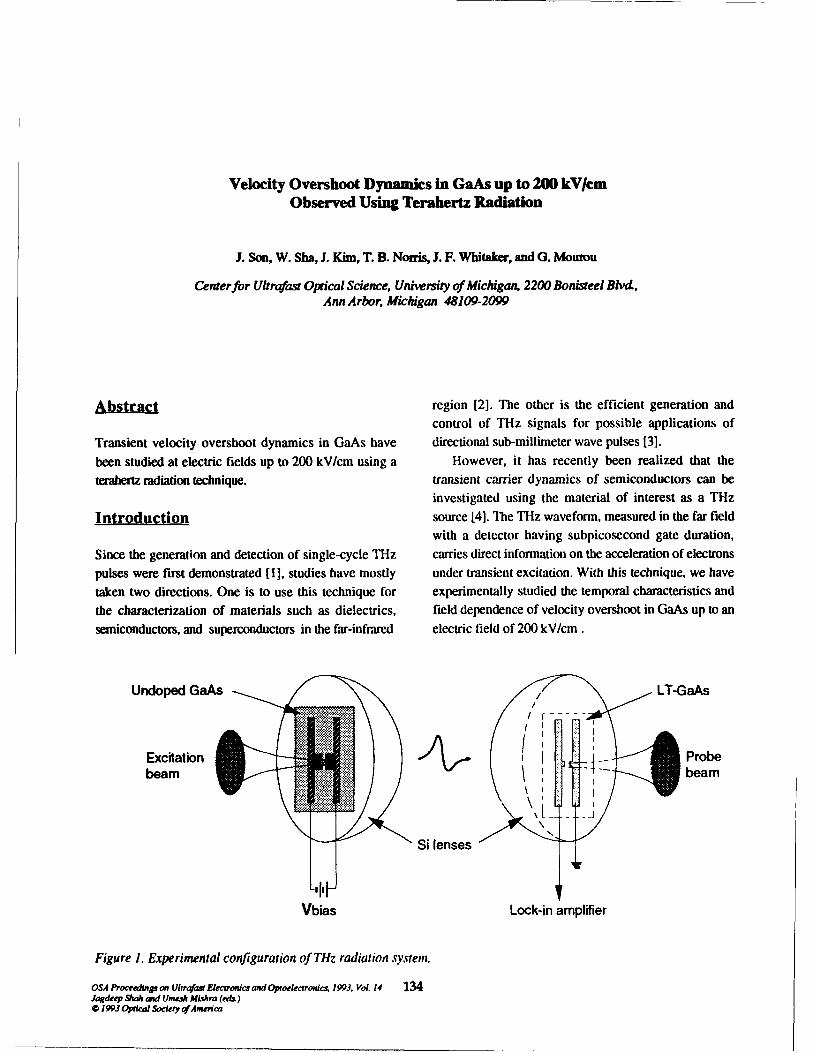
Velocity Overshoot Dynamics in GaAs up to 200 kV/cmObserved Using Terahertz Radiation
J. Son, W. Sha, J. Kim, T. B. Not-is, J. F. Whitaker, and G. Mourou
Center for Ultrafast Optical Science, University of Michigan, 2200 Bonisteel Blvd,Ann Arbor, Michigan 48109-2099
Abstract region [2]. The other is the efficient generation andcontrol of THz signals for possible applications of
Transient velocity overshoot dynamics in GaAs have directional sub-millimeter wave pulses [3].been studied at electric fields up to 200 kV/cm using a However, it has recently been realized that the
terahertz radiation technique. transient carrier dynamics of semiconductors can beinvestigated using the material of interest as a THz
Introduction source [4]. The THz waveform, measured in the far fieldwith a detector having subpicosecond gate duration,
Since the generation and detection of single-cycle THz carries direct information on the acceleration of electronspulses were first demonstrated [1], studies have mostly under transient excitation. With this technique, we have
taken two directions. One is to use this technique for experimentally studied the temporal characteristics andthe characterization of materials such as dielectrics, field dependence of velocity overshoot in GaAs up to ansemiconductors, and superconductors in the far-infrared electric field of 200 kV/cm.
UnoedG/ LT-GaAs
Excitation Probebeam JIG beam
Si lenses
Vbias Lock-in amplifier
Figure 1. Experimental configuration of THz radiation system.
OSA Procealing on Ultrrfizw Electronics and poelecrronWs 1993. Vol. 14 134Jagdeep AM and Umesh Mishra (eds.)0 1993 Opfcal Socday of America
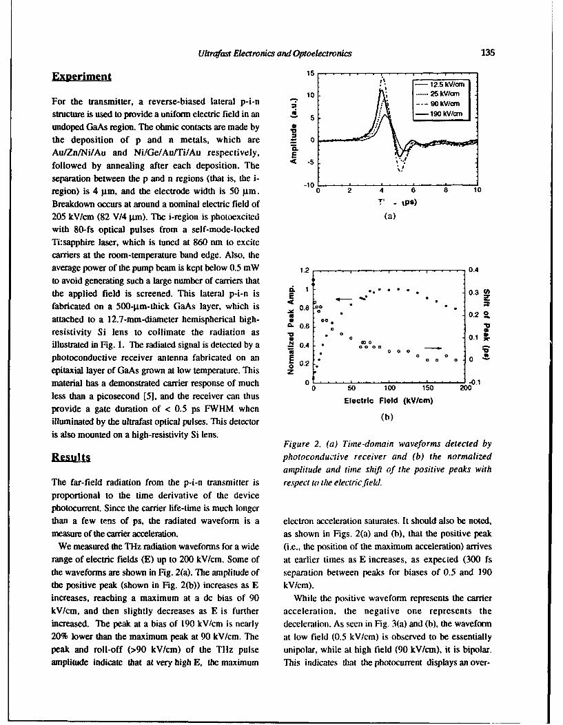
Ultrafast Electronics and Optoelectronics 135
Experiment . I ...1 2.5 kV/cm 1
10 ...... 25 kVWcmFor the transmitter, a reverse-biased lateral p-i-n 90 .. OkV/cm
structure is used to provide a uniform electric field in an . 5 190kV/CM
undoped GaAs region. The ohmic contacts are made by
the deposition of p and n metals, which are . 0
Au/Zn/Ni/Au and Ni/Ge/Au/Ti/Au respectively, Efollowed by annealing after each deposition. The -separation between the p and n regions (that is, the i-region) is 4 gm, and the electrode width is 50 im. 0 2 4 6 8 10
Breakdown occurs at around a nominal electric field of - tps)
205 kV/cm (82 V/4 im). The i-region is photoexcited (a)with 80-fs optical pulses from a self-mode-locked
Ti:sapphire laser, which is tuned at 860 nm to excite
carriers at the room-temperature band edge. Also, theaverage power of the pump beam is kept below 0.5 mW 1.2 . 0.4
to avoid generating such a large number of carriers that "& 1 .. . . •0.3 1the applied field is screened. This lateral p-i-n is E ,,,.. =fabricated on a 500-jim-thick GaAs layer, which is 0.8 0
40 0.20attached to a 12.7-mm-diameter hemispherical high- 0oa.06 o
resistivity Si lens to collimate the radiation as - , 0 0N 0.4 • o°°D0% '
illustrated in Fig. 1. The radiated signal is detected by a ! 0.4 000 0 C
photoconductive receiver antenna fabricated on an 0 0 0 0 a 000.2
epitaxial layer of GaAs grown at low temperature. This zmaterial has a demonstrated carrier response of much 0 0 50 100 150 2000.1
less than a picosecond [5], and the receiver can thus Electric Field (lcm)provide a gate duration of < 0.5 ps FWHM whenilluminated by the ultrafast optical pulses. This detector (b)is also mounted on a high-resistivity Si lens.
Figure 2. (a) Time-domain waveforms detected by
Results photoconductive receiver and (b) the normalized
amplitude and time shift of the positive peaks withThe far-field radiation from the p-i-n transmitter is respect to the electricfiek.
proportional to the time derivative of the devicephotocurrent. Since the carrier life-time is much longerthan a few tens of ps, the radiated waveform is a electron acceleration saturates. It should also be noted,measure of the carrier acceleration. as shown in Figs. 2(a) and (b), that the positive peak
We measured the THz radiation waveforms for a wide (i.e., the position of the maximum acceleration) arrivesrange of electric fields (E) up to 200 kV/cm. Some of at earlier times as E increases, as expected (300 fsthe waveforms are shown in Fig. 2(a). The amplitude of separation between peaks for biases of 0.5 and 190the positive peak (shown in Fig. 2(b)) increases as E kV/cm).increases, reaching a maximum at a dc bias of 90 While the positive waveform represents the carrierkV/cm, and then slightly decreases as E is further acceleration, the negative one represents theincreased. The peak at a bias of 190 kV/cm is nearly deceleration. As seen in Fig. 3(a) and (b), the waveform20% lower than the maximum peak at 90 kV/cm. The at low field (0.5 kV/cm) is observed to be essentiallypeak and roll-off (>90 kV/cm) of the Tttz pulse unipolar, while at high field (90 kV/cm), it is bipolar.amplitude indicate that at very high E, the maximum This indicates that the photocurrent displays an over-
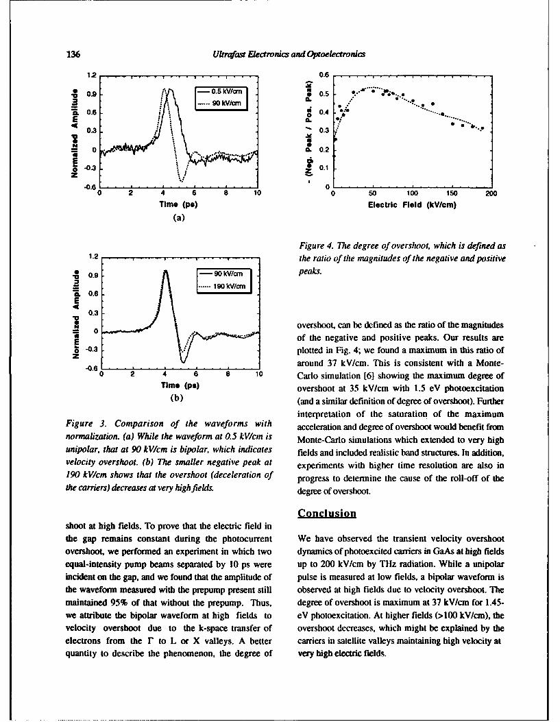
136 Ukrafost Electronics and Optoe/ectronics
1. .............................,....... 0 .6 ........ . . . . .
.~0.9 -0.5 kV/cm 0.5 ** 6..- ...... I .0.6 1 0.4
E0C0.3
Z "
.0.3 01- 0 . . . . . . *.. . . ... . . 0.02. . . . . . . .
0 2 4 6 8 10 0 50 100 150 200
Time (ps) Electric Field (kV/cm)
(a)
Figure 4. The degree of overshoot, which is defined as1.2. . ..................... ...... the ratio of the magnitudes of the negative and positive
•I peaks.90 0.9kek
...... 190 kV/cmCL 0.6
S0.3
N oovershoot, can be defined as the ratio of the magnitudes• •of the negative and positive peaks. Our results are0 -0.3 plotted in Fig. 4; we found a maximum in this ratio ofz
-0.6 around 37 kV/cm. This is consistent with a Monte-0 4 6 10 Carlo simulation [61 showing the maximum degree of
Time (pa) overshoot at 35 kV/cm with 1.5 eV photoexcitation
(b) (and a similar definition of degree of overshoot). Further
interpretation of the saturation of the maximumFigure 3. Comparison of the waveforms with acceleration and degree of overshoot would benefit fromnormalization. (a) While the waveform at 0.5 kV/cm is Monte-Carlo simulations which extended to very highunipolar, that at 90 kV/cm is bipolar, which indicates fields and included realistic band structures. In addition,velocity overshoot. (b) The smaller negative peak at experiments with higher time resolution are also in190 kV/cm shows that the overshoot (deceleration of progress to determine the cause of the roll-off of thethe carriers) decreases at very high fields. degree of overshoot.
Conclusionshoot at high fields. To prove that the electric field inthe gap remains constant during the photocurrent We have observed the transient velocity overshootovershoot, we performed an experiment in which two dynamics of photoexcited carriers in GaAs at high fieldsequal-intensity pump beams separated by 10 ps were up to 200 kV/cm by THz radiation. While a unipolarincident on the gap, and we found that the amplitude of pulse is measured at low fields, a bipolar waveform isthe waveform measured with the prepump present still observed at high fields due to velocity overshoot. Themaintained 95% of that without the prepump. Thus, degree of overshoot is maximum at 37 kV/cm for 1.45-we attribute the bipolar waveform at high fields to eV photoexcitation. At higher fields (>100 kV/cm), thevelocity overshoot due to the k-space transfer of overshoot decreases, which might be explained by theelectrons from the r to L or X valleys. A better carriers in satellite valleys maintaining high velocity atquantity to describe the phenomenon, the degree of very high electric fields.
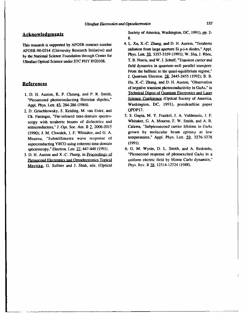
Ufraf ast Electronics and OQpoeecromnics 137
Acknowledgments Society of America, Washington, DC, 1991), pp. 2-
8.
This research is supported by AFOSR contract number 4. L. Xu, X.-C. Zhang, and D. H. Auston, "Terahertz
AFOSR-90-0214 (University Research Initiative) and radiation from large aperture Si p-i-n diodes," Appl.
by the National Science Foundation through Center for Phys. Lett. 59. 3357-3359 (1991); W. Sha, J. Rhee,
Ultrafast Optical Science under STC PHY 8920108. T. B. Norris, and W. J. Schaff, "Transient carrier andfield dynamics in quantum-well parallel transport:
From the ballistic to the quasi-equilibrium regime,"
J. Quantum Electron. 28, 2445-2455 (1992); B. B.
References Hu, X.-C. Zhang, and D. H. Auston, "Observation
of negative transient photoconductivity in GaAs," in
1. D. H. Auston, K. P. Cheung, and P. R. Smith, Technical Digest of Quantum Electronics and Laser
"Picosecond photoconducting Hertzian dipoles," Science Conference (Optical Society of America,
Appl. Phys. Lett. 45., 284-286 (1984). Washington, DC, 1991), postdeadline paper
2. D. Grischkowsky, S. Keiding, M. van Exter, and QPDP17.
Ch. Fattinger, "Far-infrared time-domain spectro- 5. S. Gupta, M. Y. Frankel, J. A. Valdmanis, J. F.
scopy with terahertz beams of dielectrics and Whitaker, G. A. Mourou, F. W. Smith, and A. R.
semiconductors," J. Opt. Soc. Am. B 7, 2006-2015 Calawa, "Subpicosecond carrier lifetime in GaAs
(1990); J. M. Chwalek, J. F. Whitaker, and G. A. grown by molecular beam epitaxy at low
Mourou, "Submillimetre wave response of temperatures," Appl. Phys. Lett. 2., 3276-3278
superconducting YBCO using coherent time-domain (1991).spectroscopy," Electron. Lett. 27, 447-448 (1991). 6. G. M. Wysin, D. L. Smith, and A. Redondo,
3. D. H. Auston and X.-C. Zhang, in Proceedings of "Picosecond response of photoexcited GaAs in a
Picosecond Electronics and Optoelectronics Topical uniform electric field by Monte Carlo dynamics,"
Mee.ia., G. Sollner and 1. Shah, eds. (Optical Phys. Rev. B 3M, 12514-12524 (1988).
Phase Relaxation Processes of Excitons in Island-Inserted Quantum Well Structures-Suppression
of Relaxation and Giant Quantum Beats
T. MatsusueInstitute of Industrial Science, University of Tokyo, 7-22-1 Roppongi,
Minato-ku, Tokyo 106, Japan
T. Saiki and K. Kuwata-GonokamiDepartment ofApplied Physics, Faculty of Engineering, University of Tokyo,
7-3-1 Hongo, Bunkyo-ku, Tokyo 113, Japan
H. AldyamiaResearch Center for Advanced Science and Technology, University of Tokyo,
4-6-1 Komaba, Meguro-ku, Tokyo 153, Japan
H. SakaiQuantum Wave Project, ERA TO, Research Development Corporation ofJapan,
4-3-24 Komaba, Meguro-ku, Tokyo 153, Japan
Abstract Ga_ s om eDegenerate four wave mixing measurements are per-formed on exciton resonance in island inserted quantumwells, where AlAs islands are embedded in the center of -
the GaAs quantum wells. It is found that the island in- - =sertion causes strong suppression of phase relaxation ofthe excitons. Deep quantum beats are also observed andattributed to coherent lateral oscillations of excitons be-tween adjacent regions with one monolayer well widthdifference. Figure 1: Schematic illustration of island-inserted quan-
tum well (I2QW).
1 Introduction apply DFWM to study AlAs island inserted GaAs QWstructures as shown in Fig. 1 to see how coherent motion
In addition to the steady interest in standard quantum of excitons in QWs is modified by the random islandswells (QWs), optical properties of novel quantum con- inserted in the center of the wells.fined structures such as quantum wires and quantum dotshave attracted increasing interests toward new phase ofphysics and future ultrafast devices. In order to tailorthe electronic states of QWs, a technique to insert a thin 2 Samplespotential layer into a QW has been proposed and at-tempted with molecular beam epitaxy (MBE) [11-[3]. For Two samples were investigated; an island-inserted QWexample, the insertion of one monolayer (ML) of AlAs or (12QW) sample and a reference sample of normal QWInAs into a GaAs QW as an repulsive or attractive poten- (NQW) without island insertion. The samples weretial pushes its energy level up or down uniformly. If the grown by MBE on (001) surfaces of semi-insulating GaAsamount inserted is a half ML, random islands of potential substrates at 600°C. After deposition of a buffer layer ofare created, which modify in-plane electronic states. If a GaAs and an AIO.3Ga0 .7As layer, 30 periods of 12QW orvicinal substrate is used, periodic modulation of the po- NQW structures were grown followed by a 200A GaAstential can be realized. We have so far investigated these cap layer. The growth sequence of one period of I2QWstructures regarding growth processes, electric transport was as follows (IML=2.83A); growth of 28ML AlAs,properties, and optical properties [1]-[4]. growth interruption for 10s, growth of 18ML GaAs, inter-
Degenerate four wave mixing (DFWM) is an efficient ruption for 60s, deposition of Al with an amount corre-technique to understand microscopic behaviors of elec- sponding to 0.5ML of AlAs, interruption for 20s, growthtronic states in condensed matter, and has been success- of 18.5ML GaAs, and interruption for 6Os. To enhancefully performed to study dynamics of excitons and free the migration of Al atom and to form large islands ofcarriers in QWs and bulk semiconductors [5, 6]. We now AlAs, migration enhanced epitaxial technique was used
OGSA Proceeding on Uirrafamt Eectronics and OpwactonkA 1993 VoL 14 138Jagdeep Shah and Umesh Mishra (edL)0 1993 Op•ical Society ofAmerica
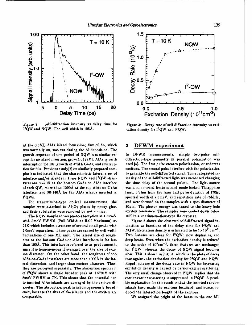
Ultrafast Nacrrnics and Optoeaectronics 139
100 " 1.5 . .
10 ... .. . . I. . 1.5 ,, . .. I. . .T= 10K T=1OK NW
S- - -------
1.01
pi0 7T "0
12-QW a:40.5
NQW W
(0 1 I•L d • . . . I . .
-5 0 5 10 15 20 0.0 0.5 1.0Delay Time (ps) Excitation Density (1 0 11cm 2)
Figure 2: Self-diffraction intensity vs delay time for Figure 3: Decay rate of self-diffraction intensity vs exci-I2QW and NQW. The well width is 105A. tation density for I2 QW and NQW.
at the 0.hML AlAs island formation; flux of As, which 3 DFWM experimentwas normally on, was cut during the Al deposition. Thegrowth sequence of one period of NQW was similar ex- In DFWM measurements, simple two-pulse self-cept for no island insertion; growth of 28ML AlAs, growth diffraction-type geometry in parallel polarization wasinterruption for 10s, growth of 37ML GaAs, and interrup- used [5]. The first pulse creates polarization, or coherenttion for 60s. Previous study[3] on similarly prepared sam- excitons. The second pulse interfere with the polarizationples has indicated that the characteristic lateral sizes of to generate the self-diffracted signal. Time integrated in-interface and/or islands in these NQW and I2QW struc- tensity of the self-diffracted light was measured changingtures are 50-70A at the bottom GaAs-on-AlAs interface the time delay of the second pulses. The light sourceof each QW, more than 1000A at the top AlAs-on-GaAs was a commercial femto-second mode-locked Ti:sapphireinterface, and 90-140A for the AlAs islands inserted in laser. Pulses from the laser had pulse duration of 170fs,12QWs. spectral width of 7.5meV, and repetition rate of 76MHz,
For transmission-type optical measurements, the and were focused on the samples with a spot diameter ofsamples were attached to A120 3 plates by epoxy glue, 80pm. The photon energy was tuned to the heavy-holeand their substrates were removed by wet etching. exciton ren~ance. The samples were cooled down below
The NQW sample shows photo-absorption at 1.559ev 10K in a continuous-flow-type He cryostat.with 5meV FWHM (Full Width at Half Maximum) at Figure 2 shows the observed self-diffracted signal in-27K which includes structure of several small peaks with tensities as functions of the delay time for 12QW and2.0meV separation. These peaks are caused by well width NQW. Excitation density is estimated to be I X 101 1 cm- 2 .fluctuations of one ML unit. The lateral size of rough- Two features are clear for 12QW: slow dephasing andness at the bottom GaAs-on-AlAs interfaces is far less deep beats. Even when the excitation density is reducedthan 100A. This interface is referred to as psudosmooth, to the order of 109 cm-2 , these features are unchangedsince it is homogeneous if averaged over the area of exci- for 12 QW, whereas the decay of NQW signal becomeston diameter. On the other hand, the roughness of top slow. This is shown in Fig. 3, which is the plots of decayAlAs-on-GaAs interfaces are more than I000A in the lat- rate against the excitation density for 12QW and NQW.eral dimension, and larger than exciton diameter. Thus, Rapid increase of the decay rate in NQW for increasingthey are perceived separately. The absorption spectrum excitation density is caused by carrier-carrier scattering.of 12QW shows a single broader peak at 1.579eV with The very small change observed in I2QW implies that the8meV FWHM at 7K. This shows that the potential due carrier-carrier scattering is suppressed in 12 QW. A possi-to inserted AlAs islands are averaged by the exciton di- ble explanation for this result is that the inserted randomameter. The absorption peak is inhomogeneously broad- islands have made the excitons localized, and hence, re-ened, because the sizes of the islands and the exciton are duced the interaction length of the excitons.comparable. We assigned the origin of the beats to the one ML
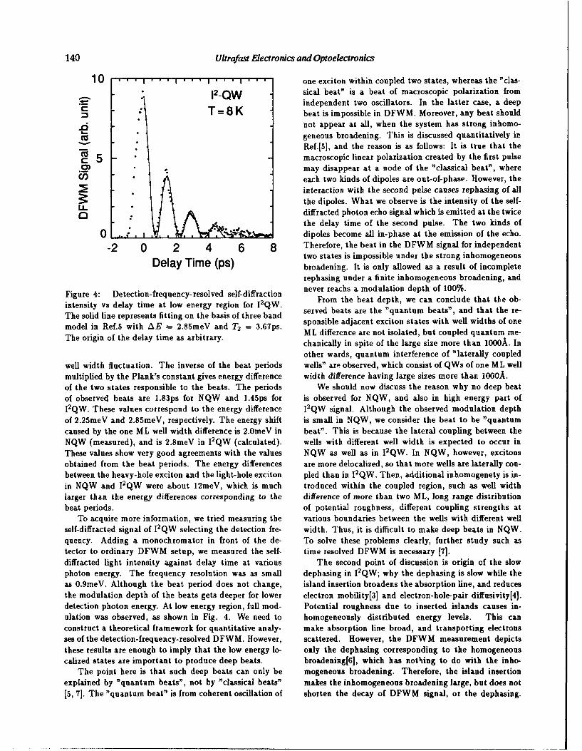
140 Ultrafast Electronics and Optoelectronics
10 . ......... ... .... one exciton within coupled two states, whereas the "clas-
12_QW sical beat" is a beat of macroscopic polarization fromST"8Kindependent two oscillators. In the latter case, a deep
"- T 8beat is impossible in DFWM. Moreover, any beat shouldnot appear at all, when the system has strong inhomo-
geneous broadening. This is discussed quantitatively in___Ref.[5], and the reason is as follows: It is true that the
c 5 " "• macroscopic linear polarization created by the first pulse
._ •may disappear at a node of the "classical beat", whereeach two kinds of dipoles are out-of-phase. However, theinteraction with the second pulse causes rephasing of all
the dipoles. What we observe is the intensity of the self-*L• diffracted photon echo signal which is emitted at the twice
• • the delay time of the second pulse. The two kinds of0 L dipoles become all in-phase at the emission of the echo.
-2 0 2 4 6 8 Therefore, the beat in the DFWM signal for independenttwo states is impossible under the strong inhomogeneous
Delay Time (ps) broadening. It is only allowed as a result of incomplete
rephasing under a finite inhomogeneous broadening, and
Figure 4: Detection-frequency-resolved self-diffraction never reachs a modulation depth of 100%.
intensity vs delay time at low energy region for I2QW. From the beat depth, we can conclude that the ob-
The solid line represents fitting on the basis of three band served beats are the "quantum beats", and that the re-
model in Ref.5 with AE = 2.85meV and T2 = 3.67ps. sponsible adjacent exciton states with well widths of one
The origin of the delay time as arbitrary. ML difference are not isolated, but coupled quantum me-chanically in spite of the large size more than 1000A. Inother wards, quantum interference of "laterally coupled
well width fluctuation. The inverse of the beat periods wells" are observed, which consist of QWs of one ML well
multiplied by the Plank's constant gives energy difference width difference having large sizes more than i000A.of the two states responsible to the beats. The periods We should now discuss the reason why no deep beatof observed beats are 1.83ps for NQW and 1.45ps for is observed for NQW, and also in high energy part of12QW. These values correspond to the energy difference 12QW signal. Although the observed modulation depthof 2.25meV and 2.85meV, respectively. The energy shift is small in NQW, we consider the beat to be "quantum
caused by the one ML well width difference is 2.0meV in beat". This is because the lateral coupling between theNQW (measured), and is 2.8meV in 12QW (calculated). wells with different well width is expected to occur inThese values show very good agreements with the values NQW as well as in I2 QW. In NQW, however, excitonsobtained from the beat periods. The energy differences are more delocalized, so that more wells are laterally cou-between the heavy-hole exciton and the light-hole exciton pled than in I2QW. Then, additional inhomogenety is in-in NQW and I2QW were about 12meV, which is much troduced within the coupled region, such as well widthlarger than the energy differences corresponding to the difference of more than two ML, long range distributionbeat periods, of potential roughness, different coupling strengths at
To acquire more information, we tried measuring the various boundaries between the wells with different well
self-diffracted signal of I2QW selecting the detection fre- width. Thus, it is difficult to make deep beats in NQW.quency. Adding a monochromator in front of the de- To solve these problems clearly, further study such astector to ordinary DFWM setup, we measured the self- time resolved DFWM is necessary [7].
diffracted light intensity against delay time at various The second point of discussion is origin of the slowphoton energy. The frequency resolution was as small dephasing in I2QW; why the dephasing is slow while theas 0.9meV. Although the beat period does not change, island insertion broadens the absorption line, and reducesthe modulation depth of the beats gets deeper for lower electron mobility[3] and electron-hole-pair diffusivity[4].detection photon energy. At low energy region, full mod- Potential roughness due to inserted islands causes in-ulation was observed, as shown in Fig. 4. We need to homogeneously distributed energy levels. This can
construct a theoretical framework for quantitative analy- make absorption line broad, and transporting electronsses of the detection-frequency-resolved DFWM. However, scattered. However, the DFWM measurement depicts
these results are enough to imply that the low energy lo- only the dephasing corresponding to the homogeneouscalized states are important to produce deep beats. broadening[6], which has nothing to do with the inho-
The point here is that such deep beats can only be mogeneous broadening. Therefore, the island insertionexplained by "quantum beats", not by "classical beats" makes the inhomogeneous broadening large, but does not
[5, 7]. The "quantum beat" is from coherent oscillation of shorten the decay of DFWM signal, or the dephasing.
Ultrafast Eeclronics and Optoe/ecrronics 141
Strictly speaking, potential roughness causes not only in- quantum wells (PI-QWs)", J. of Crystal Growth, 95,homogeneous broadening, but also localization. Proba- 60-63 (1989).bly, the localization and the shortened interaction lengthare the reason of the suppressed dephasing. [2] Jean-Yves Marzin, and Jean-Michel Girard, "Exper-
imental probing of quantum-well eigenstates", Phys.Rev. Lett., 62, 2172-2175 (1989).
4 Conclusion (3] T. Noda, J. Motohisa, and H. Sakaki, "Atomic
Degenerate four wave mixing measurements are per- structure of monolayer AlAs islands on GaAs andformed on exciton resonance in I 2QW, or island inserted its anisotropy revealed by mobility study in island-QWs, where AlAs islands are embedded in the center of inserted quantum wells", Surface Science, 267, 187-the GaAs quantum wells. The island insertion causes 190 (1992), and references therein.strong suppression of phase relaxation of the excitons. [4] T. Matsusue, H. Akiyama, and H. Sakaki, "Diffu-This means that the interaction among excitons is weak- sion of two-dimensional excitons in psuedo-randomened, most likely because of localization. Deep quantum potentials embedded in quantum well structures", 6thbeats are also observed. They are attributed to coherent Int. Conf. on Superlattices, Microstructures and Mi-lateral oscillations of excitons between adjacent regions crodevices, Tu-P-43 (Xi'an, 1992), to be publishedwith one monolayer well width difference, in Superlattices and Microstructures, and reference
therein.
Acknowledgments [5] K. Leo, E. 0. G~bel, T. C. Damen, J. Shah, S.Schmitt-Rink, W. Schifer, J. F. Muller, K. K6hler,
The authors would like to thank Dr . Ema for support- and P. Ganser, "Subpicosecond four-wave mixing ining our experiment. They also thank T. Noda, 3. Moto- GaAs/AlzGai._.As quantum wells", Phys. Rev. B15,
hisa, and Professor K. Leo for helpful discussions. This 44, 5726-5737 (1991).
work is supported by a Grant in Aid from the Ministry
of Education, Science and Culture, and by the Research [6] T. Yajima, and Y. Taira, "Spatial optical paramet-Development Corporation of Japan through the ERATO ric coupling in picosecond light pulses and transverseprogram for Quantum Wave Project. relaxation effect in resonant media", J. Phys. Soc.
Japan 47, 1620-1626 (1979).
References [7] M. Koch, J. Feldmann, G. von Plessen, E. 0. G6bel,P. Thomas, and K. Kohler, "Quantum beats versus
[1] T. Noda, M. Tanaka, and H. Sakaki, "Electron mo- polarization interference: An experimental distinc-bility and roughness scattering in potential inserted tion", Phys. Rev. Lett., 69, 3631-3634 (1992).
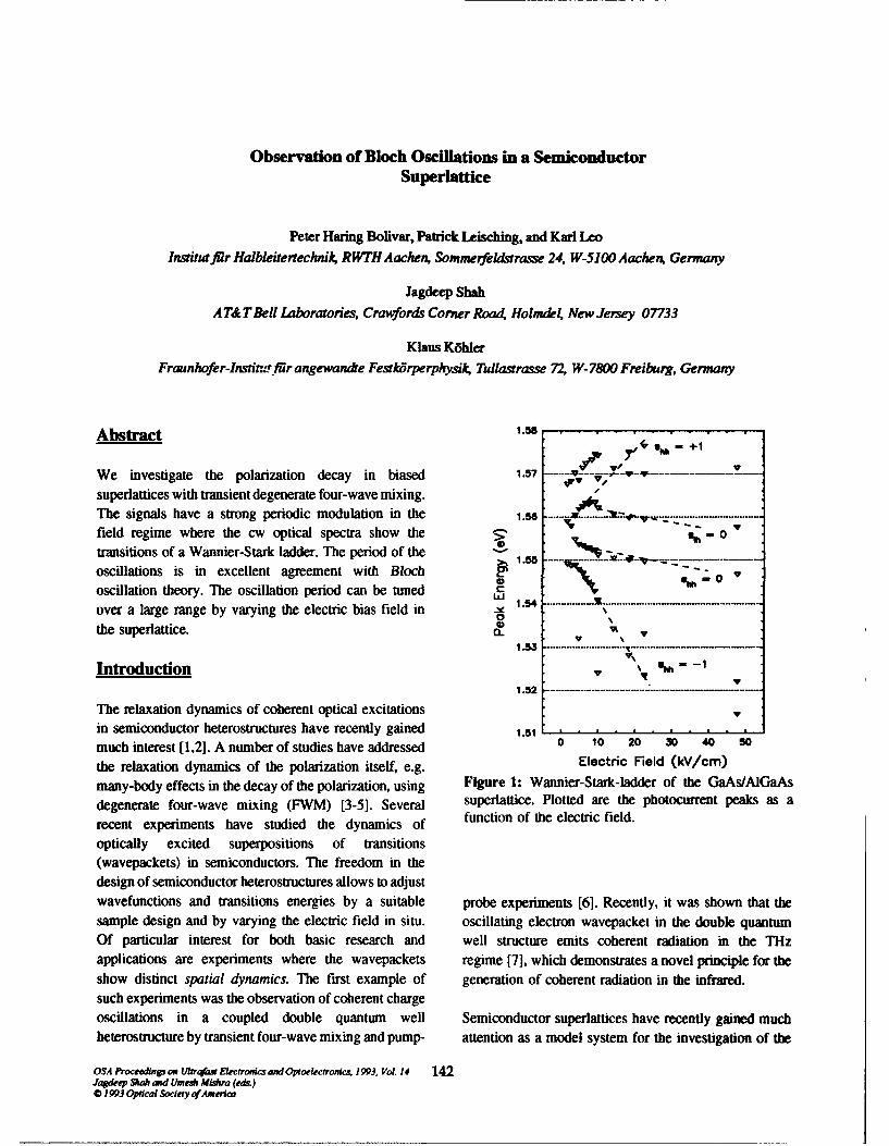
Observation of Bloch Oscillations in a SemiconductorSuperlattice
Peter Haring Bolivar, Patrick Leisching, and Karl LeoInstitutfi r Halbleitertechnik, RWTHAachen, Sommerfeldstrase 24, W-5100 Aachen, Germany
Jagdeep Shah
A T& TBell Laboratories, Crawfords Corner Roa4 Holmdel, New Jersey 07733
Klaus KghlerFraunhofer-Instit.,fiMr angewandte Festkdrperphysik, Tullastrasse 72, W-7800 Freiburg, Germany
Abstract 1.5 .. +1'"
We investigate the polarization decay in biased 1.57 ......... -...... • ... . .---..
superlattices with transient degenerate four-wave mixing.The signals have a strong periodic modulation in the 1.58 .- -"'-"'-----field regime where the cw optical spectra show the 5'V
transitions of a Wannier-Stark ladder. The period of the 1oscillations is in excellent agreement with Bloch 1 . V
oscillation theory. The oscillation period can be tuned .1 .4 ................ . ........................................ ....over a large range by varying the electric bias field in % 7the superlattice. V. I
1.53 ...................
Introduction It m1.52-------.- -.
The relaxation dynamics of coherent optical excitations Vin semiconductor heterostructures have recently gained 1.51 . ... . ...
much interest [1,2]. A number of studies have addressed 0 10 20 30 40 50
the relaxation dynamics of the polarization itself, e.g. Electrc Field (ky/cm)
many-body effects in the decay of the polarization, using Figure 1: Wannier-Stark-ladder of the GaAs/AIGaAsdegenerate four-wave mixing (FWM) [3-5]. Several superlattice. Plotted are the photocurrent peaks as a
recent experiments have studied the dynamics of function of tne electric field.
optically excited superpositions of transitions(wavepackets) in semiconductors. The freedom in thedesign of semiconductor heterostructures allows to adjustwavefunctions and transitions energies by a suitable probe experiments [6]. Recently, it was shown that thesample design and by varying the electric field in situ. oscillating electron wavepacket in the double quantumOf particular interest for both basic research and well structure emits coherent radiation in the THzapplications are experiments where the wavepackets regime [7], which demonstrates a novel principle for theshow distinct spatial dynamics. The first example of generation of coherent radiation in the infrared.such experiments was the observation of coherent chargeoscillations in a coupled double quantum well Semiconductor superlattices have recently gained muchheterostructure by transient four-wave mixing and pump- attention as a model system for the investigation of the
OSA Proceadinp on Uhkrtfst Elecronics and Optoelecrronics 1993, Vol. 14 142Jagdeep Shah and Umesh Misra (ed&)o 1993 Optical Society ofAmerica
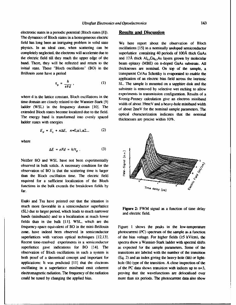
Ultrafast Electronics and Optoelectronics 143
electronic states in a periodic potential (Bloch states [8]). Results and DiscussionThe dynamics of Bloch states in a homogeneous electricfield has long been an intriguing problem in solid state We here report about the observation of Blochphysics. In an ideal case, when scattering can be oscillations [15] in a nominally undoped semiconductorcompletely neglected, the electrons will accelerate due to superlattice containing 40 periods of 1o0A thick GaAsthe electric field till they reach the upper edge of the and 17A thick Al. 3Gao.,As layers grown by molecularband. There, they will be reflected and return to the beam epitaxy (MBE) on n-doped GaAs substrate. Allinitial state. These "Bloch oscillations" (BO) in the thicknesses are nominal. On top of the sample, aBrillouin zone have a period transparent Cr/Au Schottky is evaporated to enable the
application of an electric bias field across the intrinsich (1) SL. The sample is mounted on a sapphire disk and the
substrate is removed by selective wet etching to allowexperiments in transmission configuration. Results of a
where d is the lattice constant. Bioch oscillations in the Krn-enycaultogieneetonmibd
time domain are closely related to the Wannier-Stark [9] width of about 19meV and a heavy-hole miniband width
ladder (WSL) in the frequency domain [10]. The of about 2meV for the nominal sample parameters. The
extended Bloch states become localized due to the field. opticaltcharacterization mindicates lthatrthe tnominalThe nery bnd s tansorme ino eenl spced optical characterization indicates that the nominalThe energy band is transformed into evenly spaced thicknesses are precise within 10%.
ladder states with energies
EN = E0 + nAE, n=0,±l,±2... (2)
where
AE = eFd = h/tB. (3)
Neither BO and WSL have not been experimentally 2
observed in bulk solids. A necessary condition for theobservation of BO is that the scattering time is largerthan the Bloch oscillation time. The electric fieldrequired for a sufficient localization of the Bloch 0functions in the bulk exceeds the breakdown fields by d (Ps)
far.
Esaki and Tsu have pointed out that the situation ismuch more favorable in a semiconductor superlattice Figure 2: FWM signal as a function of time delay(SL) due to larger period, which leads to much narrower and electric field.bands (minibands) and to a localization at much lowerfields than in the bulk [11]. WSL, which are thefrequency-space equivalent of BO in the mini-Brillouin Figure 1 shows the peaks in the low-temperaturezone, have indeed been observed in semiconductor photocurrent (PC) spectrum of the sample as a functionsuperlattices with various optical techniques [12,13]. of the bias voltage. For higher fields (>5 ky/cm), theRecent time-resolved experiments in a semiconductor spectra show a Wannier-Stark ladder with spectral shiftssuperlattice gave indications for BO [141. The as expected for the sample parameters. Some of theobservation of Bloch oscillations in such a system is transitions are labeled with the number of the transitionboth proof of a theoretical concept and important for (Eq. 2) and an index giving the heavy-hole (hh) or light-applications: It was predicted [111 that the electrons hole (1h) type of the transition. A close inspection of theoscillating in a superlattice miniband emit coherent of the PC data shows transition with indices up to n=3,electromagnetic radiation. The frequency of the radiation proving that the wavefunctions are delocalized overcould be tuned by changing the applied bias. more than six periods. The photocurrent data also show
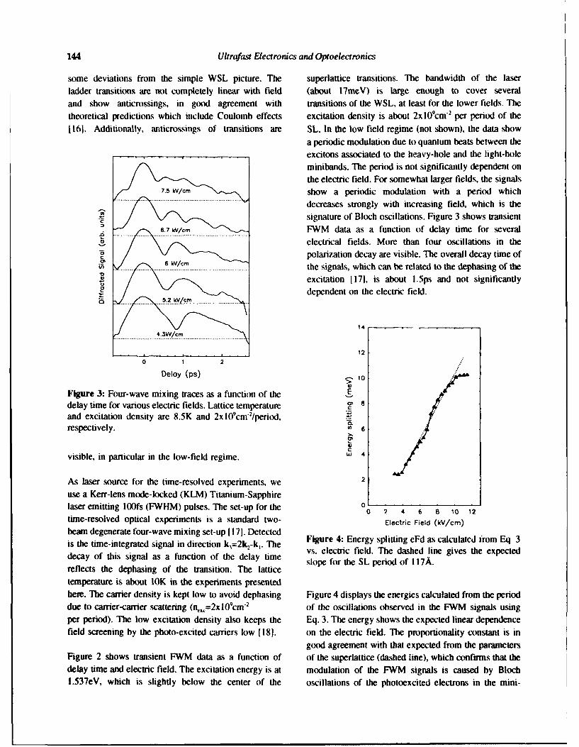
144 Ultrafast Electronics and Optoelectronics
some deviations from the simple WSL picture. The superlattice transitions. The bandwidth of the laserladder transitions are not completely linear with field (about 17meV) is large enough to cover severaland show anticrossings, in good agreement with transitions of the WSL, at least for the lower fields. Thetheoretical predictions which include Coulomb effects excitation density is about 2xl09cm 2 per period of the1161. Additionally, anticrossings of transitions are SL. In the low field regime (not shown), the data show
a periodic modulation due to quantum beats between theexcitons associated to the heavy-hole and the light-holeminibands. The period is not significantly dependent onthe electric field. For somewhat larger fields, the signals
7.5 lkv/Cn show a periodic modulation with a period which...... ........... . .decreases strongly with increasing field, which is the
r Jsignature of Bloch oscillations. Figure 3 shows transient6. ._i.-n FWM data as a function of delay time for several
electrical fields. More than four oscillations in ther polarization decay are visible. The overall decay time of
. the signals, which can be related to the dephasing of theexcitation 1171, is about 1.5ps and not significantlydependent on the electric field.
14
120 1 2
Deloy (ps) 10
Figure 3: Four-wave mixing traces as a functiom of the E
delay time for various electric fields. Lattice temperature ,P 8
and excitation density are 8.5K and 2xl0 9cm 2/period, /CL
respectively. U) 6
visible, in particular in the low-field regime. ,. 4
As laser source for the time-resolved experiments, we 2
use a Kerr-lens mode-locked (KLM) Titanium-Sapphirelaser emitting 100fs (FWHM) pulses. The set-up for the 00 2 4 6 B 10 12
time-resolved optical experiments is a standard two- Electric Field (kV/cm)
beam degenerate four-wave mixing set-up 1171. Detectedis the time-integrated signal in direction k3 =2k,-k1 . The Figure 4: Energy splitting eFd as calculated from Eq 3vs. electric field. The dashed line gives the expected
decay of this signal as a function of the delay time slope for the SL perod of 117A.reflects the dephasing of the transition. The latticetemperature is about 10K in the experiments presentedhere. The carrier density is kept low to avoid dephasing Figure 4 displays the energies calculated from the perioddue to carrier-carrier scattering (ni,=2xlOcm2 of the oscillations observed in the FWM signals usingper period). The low excitation density also keeps the Eq. 3. The energy shows the expected linear dependencefield screening by the photo-excited carriers low [181. on the electric field. The proportionality constant is in
good agreement with that expected from the parametersFigure 2 shows transient FWM data as a function of of the superlattice (dashed line), which confirms that thedelay time and electric field. The excitation energy is at modulation of the FWM signals is caused by Bloch1.537eV, which is slightly below the center of the oscillations of the photoexcited electrons in the mini-
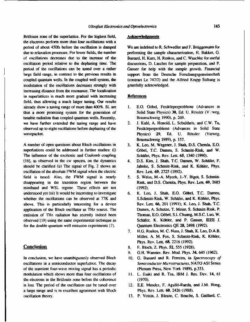
Ultrafast Electronics and Optoelectronics 145
Brillouin zone of the superlattice. For the highest field, Aoknowledgmentsthe electrons perform more than four oscillations with aperiod of about 450fs before the oscillation is damped We are indebted to R. Schwedler and F. Briggemann fordue to relaxation processes. For lower fields, the number performing the sample characterization, H. Bakker, G.of oscillations decreases due to the increase of the Bastard, H. Kurz, H. Roskos, and C. Waschke for usefuloscillation period relative to the dephasing time. The discussions, D. Laschet for sample preparation, and P.
period of the oscillations can be tuned over a rather Ganser for help with the sample growth. Financiallarge field range, in contrast to the previous results in support from the Deutsche Forschungsgemeinschaftcoupled quantum wells. In the coupled well system, the (contract Le 747/2) and the Alfried Krupp Stiftung ismodulation of the oscillations decreases strongly with gratefully acknowledged.increasing distance from the resonance. The localizationin superlattices is much more gradual with increasing Referencesfield, thus allowing a much larger tuning. Our resultsalready show a tuning range of more than 400%. SL are 1. E.O. G~bel, FestkOrperprobleme (Advances inthus a more promising system for the generation of Solid State Physics) 30, Ed. U. Rossler (V .weg,tunable radiation than coupled quantum wells. Recently, Braunschweig 1990), p. 269.we have further extended the tuning range and have 2. J. Kuhl, A. Honold, L. Schultheis, and C.W. Tu,
observed up to eight oscillations before dephasing of the Festkorperprobleme (Advances in Solid Statewavepacket. Physics) 29, Ed. U. Rossler (Vieweg,
Braunschweig 1989), p. 157.A number of open questions about Bloch oscillations in 3. K. Leo, M. Wegener, J. Shah, D.S. Chemla, E.O.
superlattices could be addressed in further studies: (i) G(bel, T.C. Damen, S. Schmitt-Rink, and W.The influence of the excitonic and Coulomb coupling Schafer, Phys. Rev. Lett. 65, 1340 (1990).
(161, as observed in the cw spectra, on the dynamics 4. D.S. Kim, J. Shah, T.C. Damen, W. Schifer, F.should be clarified (ii) The signal of Fig. 2 shows an Jahnke, S. Schmitt-Rink, and K. Kdhler, Phys.oscillation of the absolute FWM signal when the electric Rev. Lett. 69, 2725 (1992).field is tuned. Also, the FWM signal is nearly 5. S. Weiss, M.-A. Mycek, J.-Y. Bigot, S. Schmitt-
disappearing in the transition region between the Rink, and D.S. Chemla, Phys. Rev. Lett. 69, 2685miniband and WSL regime These effects are not (1992).
understood yet (iii) It would be interesting to investigate 6. K. Leo, J. Shah, E.O. Gdbel, T.C. Damen,whether the oscillations can be observed at 77K and S.Schmitt-Rink, W. Schafer, and K. KOhler, Phys.
above. This is particularly interesting for a device Rev. Lett. 66, 201 (1991); K. Leo, J. Shah, T.C.application of the Bloch oscillator as THz source. The Damen, A. Schulze, T. Meier, S. Schmitt-Rink, P.
emission of THz radiation has recently indeed been Thomas, E.O. GObel, S.L Chuang, M.S.C. Luo, W.observed 1191 using the same experimental technique as Schafer, K. K6hler, and P. Ganser, IEEE J.for the double quantum well emission experiments [7]. Quantum Electronics QE 28, 2498 (1992).
7. H.G. Roskos, M. C. Nuss, J. Shah, K. Leo, D.A.B.Miller, A. M. Fox, S. Schmitt-Rink, K. Kdhler,Phys. Rev. LetL 68, 2216 (1992).
Conclusion 8. F. Bloch, Z. Phys. 52, 555 (1928).
9. G.H. Wannier, Rev. Mod. Phys. 34, 645 (1962).In conclusion, we have unambiguously observed BIoch 10. G. Bastard and R. Ferreira, in Spectroscopy of
oscillations in a semiconductor superlattice. The decay Semiconductor Microstructures, NATO ASI Seriesof the transient four-wave mixing signal has a periodic (Plenum Press, New York 1989), p.3 3 3 .modulation which shows more than four oscillations of 11. L. Esaki and R. Tsu, IBM J. Res. Dev. 14, 61the electrons in the Brillouin zone before the coherence (1970).is lost. The period of the oscillation can be tuned over 12. E.E. Mendez, F. AgulI6-Rueda, and J.M. Hong,
a large range and is in excellent agreement with Bloch Phys. Rev. Lett. 60, 2426 (1988).oscillation theory. 13. P. Voisin, J. Bleuse, C. Bouche, S. Gaillard, C.
146 Ultrafast Electronics and Optoelectronics
Alibert, and A. Regreny, Phys. Rev. Lett. 61, 1639 84, 943 (1992).(1988). 16. M.M. Dignam and J.E. Sipe, Phys. Rev. Lett. 64,
14. J. Feldmann, K. Leo, J. Shah, D.A.B. Miller, J. E. 1797 (1990).Cunningham, S. Schmitt-Rink, T. Meier, G. von 17. T. Yajima, and Y. Taira, J. Opt. Soc. Jpn. 47, 1620Plessen, A. Schulze, and P. Thomas, Phys. Rev. B (1979).46, 7252 (1992); K. Leo, J. Feldmann, J. Shah, S. 18. The fields for the time-resolved data have beenSchmitt-Rink, J.E. Cunningham, D.A.B. Miller, corrected for the screening effects. A detailedProc. 8th International Quantum Electronics inveatigation of the field screening will beConference, Vienna 1992, p. 248. published elsewhere.
15. K. Leo, P. Haring Bolivar, F. Bruggemann, R. 19. C. Waschke et al., submitted for publication.Schwedler, and K. K6hler, Solid State Commun.
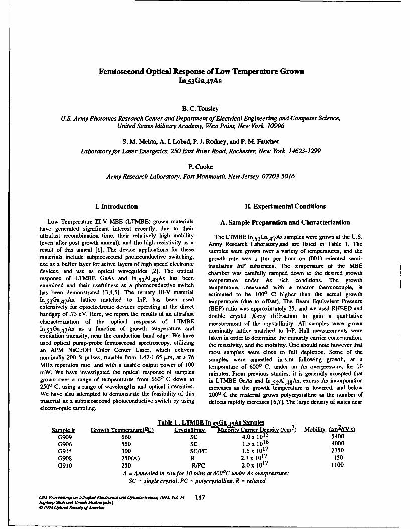
Femtosecond Optical Response of Low Temperature GrownInh3Ga.47As
B. C. TousleyU.S. Army Photonmcs Research Center and Department of Electrical Engineering and Computer Science,
United States Military Academy, West Point, New York 10996
S. M. Mehta, A. 1. Lobad, P. J. Rodney, and P. M. Fauchet
Laboratory for Laser Energetics, 250 East River Road, Rochester, New York 14623-1299
P. Cooke
Army Research Laboratory, Fort Monmouth, New Jersey 07703-5016
I. Introduction H. Experimental Conditions
Low Temperature rn-V MBE (LTMBE) grown materials A. Sample Preparation and Characterizationhave generated significant interest recently, due to theirultrafast recombination time, their relatively high mobility The LTMBE In.5 3 Ga.47 As samples were grown at the U.S.(even after post growth anneal), and the high resistivity as a Army Research Laboratory,and are listed in Table 1. Theresult of this anneal [1]. .The device applications for these samples were grown over a variety of temperatures, and thematerials include subpicosecond photoconductive switching, growth rate was 1 p.m per hour on (001) oriented semi-use as a buffer layer for active layers of high speed electronic insulating InP substrates. The temperature of the MBEdevices, and use as optical waveguides [2]. The optical chamber was carefully ramped down to the desired growthresponse of LTMBE GaAs and In.5 2 Al.4 8As has been temperature under As rich conditions. The growthexamined and their usefulness as a photoconductive switch temperature, measured with a reactor thermocouple, is
has been demonstrated 13,4,5]. The ternary Il-V material estimated to be 1000 C higher than the actual growthIn. 53Ga.4 7 As, lattice matched to InP, has been used temperature (due to offset). The Beam Equivalent Pressureextensively for optoelectronic devices operating at the direct (BEP) ratio was approximately 35, and we used RHEED andbandgap of .75 eV. Here, we report the results of an ultrafast double crystal X-ray diffraction to gain a qualitativecharacterization of the optical response of LTMBE measurement of the crystallinity. All samples were grownIn. 53 Ga.47 As as a function of growth temperature and nominally lattice matched to lnP. Hall measurements wereexcitation intensity, near the conduction band edge. We have taken in order to determine the minority carrier concentration,used optical pump-probe femtosecond spectroscopy, utilizing the resistivity, and the mobility. One should note however thatan APM NaCI:OH Color Center Laser, which delivers most samples were close to full depletion. Some of thenominally 200 fs pulses, tunable from 1.47-1.65 prm, at a 76 samples were annealed in-situ following growth, at aMHz repetition rate, and with a usable output power of 100 temperature of 6000 C, under an As overpressure, for 10mW. We have investigated the optical response of samples minutes. From previous studies, it is generally accepted thatgrown over a range of temperatures from 6600 C down to in LTMBE GaAs and n.5 2 A. 48 As, excess As incorporation2500 C, using a range of wavelengths and optical intensities, increases as the growth temperature is lowered, and belowWe have also attempted to demonstrate the feasibility of this 2000 C the material grows polycrystalline as the number ofmaterial as a subpicosecond photoconductive switch by using defects rapidly increases [6,7]. The large density of states nearelectro-optic sampling.
Table 1 . LTMBE Ins•.aA. mSml# Growth Tem~rature(Q Cirystalliniv -miority Carrier Densiy Ucm-31 Mo.bili kmj2&.V_
G909 660 SC 4.0 x 10 5400G906 550 SC 1.5 x 10¹⁶ 4000G915 300 SC/PC I.5 x 1017 2350G908 250(A) R 2.7 x 10¹⁷ 150G910 250 R/PC 2.0 x 10¹⁷ 1100
A = Annealed in-situfor 10 mins at 6000C under As overpressure;SC = single crystal, PC = polycrystalline, R = relaxed
OSAProcradng on U1hq42M Ekark sj)d,0pookevc 1993, VoL 14 147Jmdep m and Ume MWkr (ez•)* 1993 Oprid So&•"y c(Anriua
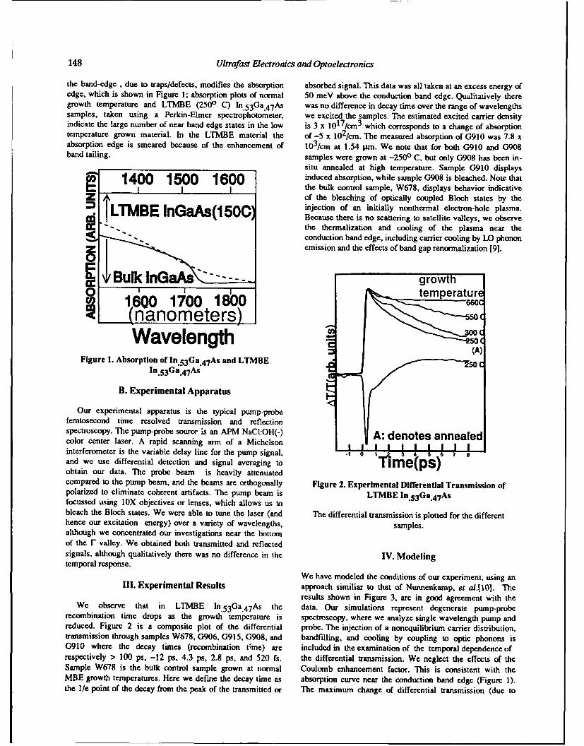
148 Ultrafast Electronics and Optoelectronics
the band-edge , due to traps/defects, modifies the absorption absorbed signal. This data was all taken at an excess energy ofedge, which is shown in Figure 1; absorption plots of normal 50 meV above the conduction band edge. Qualitatively theregrowth temperature and LTMBE (250 C) In. 5 3Ga.4 7 As was no difference in decay time over the range of wavelengthssamples, taken using a Perkin-Elmer spectrophotometer, we excited the samples. The estimated excited carrier densityindicate the large number of near band edge states in the low is 3 x 10¹⁷/cm 3 which corresponds to a change of absorptiontemperature grown material. In the LTMBE material the of -5 x 10²/cm. The measured absorption of G910 was 7.8 xabsorption edge is smeared because of the enhancement of 103/cm at 1.54 Pm. We note that for both G910 and G908band tailing. samples were grown at --250° C, but only G908 has been in-
situ annealed at high temperature. Sample G910 displays
1400 1500 1600 induced absorption, while sample G908 is bleached. Note thatthe bulk control sample, W678, displays behavior indicative
=of the bleaching of optically coupled Bloch states by theLTMBE GaAs(150C) injection of an initially nonthermal electron-hole plasma.
BIn Acausi there is no scattering to satellite valleys, we observe"*-* the thermalization and cooling of the plasma near the
"conduction band edge, including carrier cooling by LO phononemsinand the effects of band gap renormalization [9].
•1 lBulk InGAS growth
II~ b temperature1.600 1700 180 t m r u(nanometers) 0CWavelength - (A)
Figure 1. Absorption of In. 53 Ga.4 7As and LTMBEIn.53 Ga 4 7 As
B. Experimental Apparatus
Our experimental apparatus is the typical pump-probefemtosecond time resolved transmission and reflectionspectroscopy. The pump-probe source is an APM NaCI:OH(-) A: denotes annealedcolor center laser. A rapid scanning arm of a Michclson denoteLIII I I I I I I I Iinterferometer is the variable delay line for the pump signal. -1 0 it 3455 7 8and we use differential detection and signal averaging to I me(ps)obtain our data. The probe beam is heavily attenuatedcompared to the pump beam, and the beams are orthogonally Figure 2. Experimental Differential Transmission ofpolarized to eliminate coherent artifacts. The pump beam is LTMBE In.5 3 Ga.4 7Asfocussed using lOX objectives or lenses, which allows us tobleach the Bloch states. We were able to tune the laser (and The differential transmission is plotted for the differenthence our excitation energy) over a variety of wavelengths, samples.although we concentrated our investigations near the bottomof the r valley. We obtained both transmitted and reflectedsignals, although qualitatively there was no difference in the IV. Modelingtemporal response.
We have modeled the conditions of our experiment, using anIII. Experimental Results approach similiar to that of Nurmenkamp, el al.[lO[. The
results shown in Figure 3, are in good agreement with theWe observe that in LTMBE ln. 53 Ga.4 7 As the data. Our simulations represent degenerate pump-probe
recombination time drops as the growth temperature is spectroscopy, where we analyze single wavelength pump andreduced. Figure 2 is a composite plot of the differential probe. The injection of a nonequilibrium carrier distribution.transmission through samples W678, G906, G915, G908, and bandfilling, and cooling by coupling to optic phonons isG910 where the decay times (recombination 0me) are included in the examination of the temporal dependence ofrespectively > 100 ps, -12 ps, 4.3 ps, 2.8 ps, and 520 fs. the differential transmission. We neglect the effects of theSample W678 is the bulk control sample grown at normal Coulomb enhancement factor. This is consistent with theMBE growth temperatures. Here we define the decay time as absorption curve near the conduction band edge (Figure 1).the l/e point of the decay from the peak of the transmitted or The maximum change of differential transmission (due to
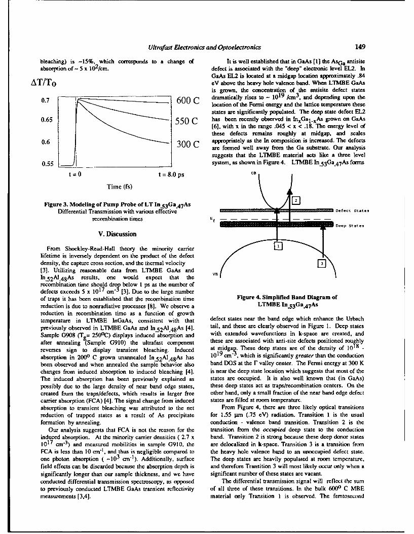
Ultrafast Electronics and Optoelectronics 149
bleaching) is ~15%, which corresponds to a change of It is well established that in GaAs [1] the ASGa antisiteabsorption of - 5 x 10²/cm. defect is associated with the "deep" electronic level EL2. In
GaAs EL2 is located at a midgap location approximately .84AT/To eV above the heavy hole valence band. When LTMIBE GaAs
is grown, the concentration of the antisite defect states
0.7 I 600 C dramatically rises to - 1019 /cm 3, and depending upon thelocation of the Fermi energy and the lattice temperature thesestates are significantly populated. The deep state defect EL2
0.65 550 C has been recently observed in InxGal-xAs grown on GaAs[61, with x in the range .045 < x < .18. The energy level ofthese defects remains roughly at midgap, and scales
0.6 300 C appropriately as the In composition is increased. The defectsare formed well away from the Ga substrate. Our analysissuggests that the LTMBE material acts like a three level
0.55 -J system, as shown in Figure 4. LTMBE In.5 3 Ga.4 7 As forms
t =0 t 8.Ops c
Time (fs)
Figure 3. Modeling of Pump Probe of LT In.5 3 Ga.47 As D S
Differential Transmission with various effective Defect States
recombination times E
Deep States
V. Discussion
From Shockley-Read-Hall theory the minority carrierlifetime is inversely dependent on the product of the defectdensity, the capture cross section, and the thermal velocity[3]. Utilizing reasonable data from LTMBE GaAs andIn. 52 AI.4 8 As results, one would expect that therecombination time should drojy below I ps as the number ofdefects exceeds 5 x 1017 cm1 [3]. Due to the large numberof traps it has been established that the recombination time Figure 4. Simplified Band Diagram ofreduction is due to nonradiative processes [8]. We observe a LTMBE In.5 3 Ga.4 7 Asreduction in recombination time as a function of growthtemperature in LTMBE InGaAs, consistent with that defect states near the band edge which enhance the Urbachpreviously observed in LTMBE GaAs and In.5 2Al.4 8 As [4]. tail, and these are clearly observed in Figure 1. Deep statesSample G908 (Tg= 2500 C) displays induced absorption and with extended wavefunctions in k-space are created, andafter annealing (Sample G910) the ultrafast compenent these are associated with anti-site defects positioned roughlyreverses sign to display transient bleaching. Induced at midgap. These deep states are of the density of 10 8-
absorption in 2000 C grown unannealed In.52 Al.4 8 As has 1019 cm", which is significantly greater than the conductionbeen observed and when annealed the sample behavior also band DOS at the r valley center. The Fermi energy at 300 Kchanges from induced absorption to induced bleaching [4]. is near the deep state location which suggests that most of theThe induced absorption has been previously explained as states are occupied. It is also well known that (in GaAs)possibly due to the large density of near band edge states, these deep states act as traps/recombination centers. On thecreated from the traps/defects, which results in larger free other hand, only a small fraction of the near band edge defectcarrier absorption (FCA) [4]. The signal change from induced states are filled at room temperaturc.absorption to transient bleaching was attributed to the net From Figure 4, there are three likely optical transitionsreduction of trapped states as a result of As precipitate for 1.55 pim (.75 eV) radiation. Transition 1 is the usualformation by annealing, conduction - valence band transition. Transition 2 is the
Our analysis suggests that FCA is not the reason for the transition from the occupied deep state to the conductioninduced absorption. At the minority carrier densities ( 2.7 x band. Transition 2 is strong because these deep donor states1017 cm-3 ) and mcasured mobilities in sample G910, the are delocalized in k-space. Transition 3 is a transition fromFCA is less than 10 cm"1, and thus is negligible compared to the heavy hole valence band to an unoccupied defect state.one photon absorption ( -103 cm-1 ). Additionally, surface The deep states are heavily populated at room temperature,field effects can be discarded because the absorption depth is and therefore Transition 3 will most likely occur only when asignificantly longer than our sample thickness, and we have significant number of these states are vacant.conducted differential transmission spectroscopy, as opposed The differential transmission signal will reflect the sumto previously conducted LTMBE GaAs transient rcflectivity of all three of these transitions. In the bulk 6000 C MItEmeasurements [3,41. material only Transition I is observed. The femtosecond
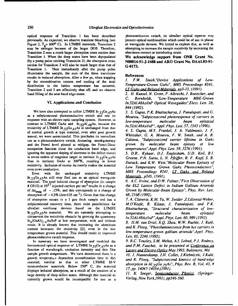
150 Ultrafast Electronics and Optoelectronics
optical response of Transition 1 has been described photoconductive switch, its ultrafast optical reponse maypreviously. As expected, we observe transient bleaching (see present optical nonlinearities which could be of use in planarFigure 2, Tg- 6000 C). In LTMBE materials, Transition 2 or waveguide devices. We intend to explore this, as well asmay be stronger because of the larger DOS. Therefore, attempting to increase the sample resistivity by increasing theTransition 2 sees a much larger absorption cross section than aluminum content or introducing strain.Transition 1. When the deep states have been depopulated We acknowledge support from ONR Grant No.(by a pump pulse exciting Transition 2), the absorption cross N00014-91-J-1488 and ARO Grant No. DAAL03-91-section for Transition 3 will also be much larger than that of G-0173.Transition 1. Thus immediately after the pump pulseilluminates the sample, the sum of the three transitionsresults in induced absorption. After a few ps, when trappingby the recombination centers and cooling of the total 1. F.W. Smith,"Device Applications of Low-
distribution to the lattice temperature has occurred, Temperature-Grown GaAs", MRS Proceedings #241,
Transition 2 and 3 are effectively shut off, and we observe LT GaAs and Related Mdterials, pp3-12, (1991)band filling of the near band edge states. 2. H. Kunzel, N. Grote, P. Albrecht, J. Boettcher, and
C. Bornholdt, "Low-Temperature MBE-GrownVI. Applications and Conclusion In.52AI.48AslInP Optical Waveguides",Elect. Lett. 28,
844 (1992).We have also attempted to utilize LTMBE In.5 3Ga.4 7 As 3. S. Gupta, P.K. Bhattacharya, J. Panulapati, and G.
as a subpicosecond photoconductive switch and test its Mourou, "Subpicosecond photoresponse of carriers inresponse with an electro-optic sampling system. However, in low-temperature molecular beam epitaxialcontrast to LTMBE GaAs and In.5 2AI.4 8 As, because the In.52Al.48AsllnP", Appl. Phys. Lett. 57, 1543 (1990).resistivity of LTMBE In.5 3Ga.4 7 As is unchanged from thatof normal growth n type material, even after post growth . S. Gupta, M.Y. Frankel, J. A. Valdmanis, J. F.anneal, we were unsuccessful. This precludes its immediate Whittaker, G. A. Mourou, F. W. Smith, and A. R.
use as a photoconductive switch. Assuming nondegencracy Calawa, "Subpicosecond carrier lifetime in GaAsand the Fermi level pinned at midgap, the Fermi-Dirac grown by molecular beam epitaxy at lowoccupation function (near the conduction band edge, and temperatures",Appl. Phys. Lett. 59,3276 (1991).ignoring the apparent doping of electrons in the defect states) 5. D.R.. Kykaar, D.J. Eaglesham, U.D. Keil, B.I.is seven orders of magnitue larger in intrinsic In. 53 Ga.4 7 As Greene, P.N. Saeta, L. N. Pfeiffer, R. F. Kopf, S. B.than in intrinsic GaAs at 300 0K, resulting in lower Darack, and K.W. West,"Molecular Beam Epitaxy ofresistivity. Inclusion of excess As merely makes the material Low Temperature Grown GaAs Photoconductors",even more conductive.
Even with the unchanged resistivity LTMBE MRS Proceedings #241, IT GaAs and RelatedIn. 53 Ga.4 7 As still may find use as an optical waveguide Minals,, p245, (1991).material. The total induced change of absorption (in sample 6. A.C. Irvine, and D.W. Palmer,"First Observation of# G910) at 1017 injected carriers per cm3 results in a change the EL2 Lattice Defect in Indium Gallium Arsenideof Animag of ~ .15%, and this corresponds to a change of Grown by Molecular-Beam Epitaxy", Phys. Rev. Lett.absorption of - 4.5% (Aa=135 cr- 1 ). Given that this change 68, 2168 (1992).of absorption occurs in a 1 p.tm thick sample and has a 7. A. Claverie, K.M. Yu, W. Swider ,Z.Liliental-Weber,subpicosecond recovery time, there exist possibilities for M.O'Keefe, R. Kilaas, J. Pamulapati, and P.K.ultrafast nonlinear devices based on the LTMBE Bhattacharya, "Structural characterization of low-In. 53 Ga.4 7 As material. We are currently attempting to temperature molecular beam epitaxialcircumvent the resistivity obstacle by growing the quartenary In.52Al.48AsIlnP",Appl. Phys. Lett. 60, 989 (1992)Inx(GaAl)l-xAs/InP at low temperature, with and without 8. H.M. van Driel, X.Q. Zhou, W.W. Ruehle, J. Kuhl,strain. It is already known that increasing the aluminumcontent increases the resistivity [2], even in the low and K. Ploog, "Photoluminescencefrom hot carriers intemperature grown material. This should result in improved low-temperature-grown gallium arsenide"Appl. Phys.
photoconductive switch response. Lett. 60,2246 (1992).In summary we have investigated and modeled the 9. B.C. Tousley, S.M. Mehta, A.I. Lobad, P.J. Rodney,
femtosecond optical response of LTMBE In. 5 3Ga.47 As as a and P.M. Fauchet, to be presented at Conference onfunction of wavelength, excitation intensity and thin film Lasers and Electro-Optics May 1993, Baltimore, Mdsample growth temperature. We have determined there is a 10. J. Nunnenkamp, J.l. Collet, J.Klebniczki. J.Kuhl,growth temperatue dependent recombination time in this and K. Ploog, "Subpicosecond kinetics of band-edgematerial, similiar to that in other LTMBE lll-V absorption in Alsemiconductor materials. Below 2500 C, the material a2SGa.7SAs', Phys. Rev. B. Vol. 43, #
displays induced absorption, as a result of the creation of a 17, pp. 14047-14054,(1991).
large density of deep defect states. Although this material as 11. K. Seeger, Semiconductor Physics, (Springer-
currently grown would be incompatible for use as a Verlag, New York,1991), pp346-360.
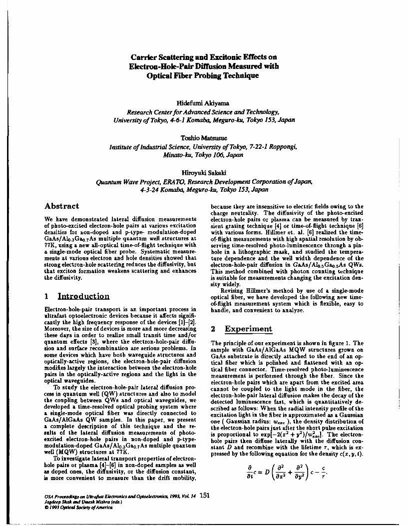
Carrier Scattering and Excitonic Effects onElectron-Hole-Pair Diffusion Measured with
Optical Fiber Probing Technique
Hidefumi Aidyama
Research Center for Advanced Science and Technology,University of Tokyo, 4-6-1 Komaba, Meguro-lk, Tokyo 153, Japan
Toshio Matsusue
Institute of Industrial Science, University of Tokyo, 7-22-1 Roppongi,Minato-kla, Tokyo 106, Japan
Hiroyuki Sakaki
Quantum Wave Project, ERA TO, Research Development Corporation of Japan,4-3-24 Komaba, Meguro-ku, Tokyo 153, Japan
Abstract because they are insensitive to electric fields owing to thecharge neutrality. The diffusivity of the photo-excited
We have demonstrated lateral diffusion measurements electron-hole pairs or plasma can be measured by tran-of photo-excited electron-hole pairs at various excitation sient grating technique [4] or time-of-flight technique [6]densities for non-doped and p-type- modulation-doped with various forms. Hillmer et. al. [6] realized the time-GaAs/AIo.3 Gao.7As multiple quantum well structures at of-flight measurements with high spatial resolution by ob-77K, using a new all-optical time-of-flight technique with serving time-resolved photo-luminescence through a pin-a single-mode optical fiber probe. Systematic measure- hole in a lithographic mask, and studied the tempera-ments at various electron and hole densities showed that ture dependence and the well width dependence of thestrong electron-hole scattering reduces the diffusivity, but electron-hole-pair diffusion in GaAs/Alo.sGao.sAs QWs.that exciton formation weakens scattering and enhances This method combined with photon counting techniquethe diffusivity. is suitable for measurements changing the excitation den-
sity widely.Revising Hillmer's method by use of a single-mode
1 Introduction optical fiber, we have developed the following new time-of-flight measurement system which is flexible, easy to
Electron-hole-pair transport is an important process in handle, and convenient to analyze.ultrafast optoelectronic devices because it affects signifi-cantly the high frequency response of the devices [1]-[2].Moreover, the size of devices is more and more decreasing 2 Experimentthese days in order to realize small transit time and/orquantum effects [3], where the electron-hole-pair diffu- The principle of our experiment is shown in figure 1. Thesion and surface recombination are serious problems. In sample with GaAs/AlGaAs MQW structures grown onsome devices which have both waveguide structures and GaAs substrate is directly attached to the end of an op-optically-active regions, the electron-hole-pair diffusion tical fiber which is polished and flattened with an op-modifies largely the interaction between the electron-hole tical fiber connector. Time-resolved photo-luminescencepairs in the optically-active regions and the light in the measurement is performed through the fiber. Since theoptical waveguides. electron-hole pairs which are apart from the excited area
To study the electron-hole-pair lateral diffusion pro- cannot be coupled to the light mode in the fiber, thecess in quantum well (QW) structures and also to model electron-hole-pair lateral diffusion makes the decay of thethe coupling between QWs and optical waveguides, we detected luminescence fast, which is quantitatively de-developed a time-resolved optical probing system where scribed as follows: When the radial intensity profile of thea single-mode optical fiber was directly connected to excitation light in the fiber is approximated as a GaussianGaAs/AlGaAs QW samples. In this paper, we present one ( Gaussian radius: wuc ), the density distribution ofa complete description of this technique and the re- the electron-hole pairs just after the short pulse excitationsuits of the lateral diffusion measurements of photo- is proportional to exp[-2(z 2 + y2)/w2]. The electron-excited electron-hole pairs in non-doped and p-type- hole pairs then diffuse laterally with the diffusion con-modulation-doped GaAs/A10.3Gao.7 As multiple quantum stant D and recombine with the lifetime r, which is ex-well (MQW) structures at 77K. pressed by the following equation for the density c(x, y, t).
To investigate lateral transport properties of electron-hole pairs or plasma [4]-[6] in non-doped samples as well 6 a2 0 2 \ cas doped ones, the diffusivity, or the diffusion constant, -c = D +cis more convenient to measure than the drift mobility, 19 6X
2 8 -21 r
OSA Proceedas on Ukrnaf Ekaronics and Optoekearmci 1991. VoL 14 151Jag deep Shah and Umesh Mwhra (edo)0 1993 Optical Sockty ofAnierica
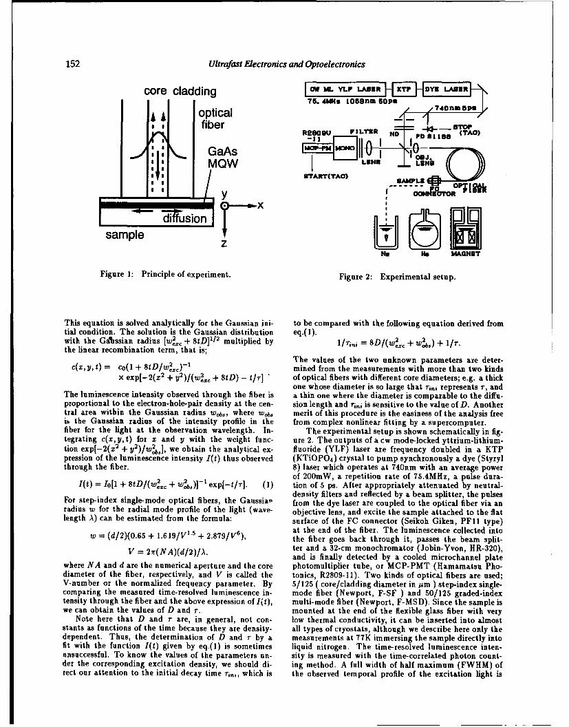
152 Ultrafast Electronics and Optoelectronics
core cladding COW MAD75. 4UHN 1058nm 50Ps
A A optical / 7740nM5P
fiber - _o- --R2809U FILTER ND P -I11s (TA•)
:mo MQW A L I LNEt
ma : INR LEO, , .. .. ~. o,71g
dixusionsample
Z
MR He MAGNET
Figure 1: Principle of experiment. Figure 2: Experimental setup.
This equation is solved analytically for the Gaussian ini- to be compared with the following equation derived fromtial condition. The solution is the Gaussian distribution eq.(1).with the Ga¶ssian radius [w2 + 8tD]11 2 multiplied by l/-,,, = 8D/(wc + W2 ) + 1/r.
the linear recombination term, that is;
The values of the two unknown parameters are deter-c(z, y, t) = c0(l + 8tD/w~)- 1 mined from the measurements with more than two kinds
x exp[-2(z 2 + Y 2 )/(w2z• + 8tD) - t/r] of optical fibers with different core diameters; e.g. a thickone whose diameter is so large that ri,,i represents r, and
The luminescence intensity observed through the fiber is a thin one where the diameter is comparable to the diffu-proportional to the electron-hole-pair density at the cen- sion length and ri,, is sensitive to the value of D. Anothertral area within the Gaussian radius wtb., where wtob merit of this procedure is the easiness of the analysis freeis the Gaussian radius of the intensity profile in the from complex nonlinear fitting by a supercomputer.fiber for the light at the observation wavelength. In- The experimental setup is shown schematically in fig-tegrating c(z,yt,t) for z and y with the weight func- ure 2. The outputs of a cw mode-locked yttrium-lithium-tion exp[-2(z 2 + y2)/WtoJ, we obtain the analytical ex- fluoride (YLF) laser are frequency doubled in a KTPpression of the luminescence intensity I(t) thus observed (KTiOPO 4) crystal to pump synchronously a dye (Styrylthrough the fiber. 8) laser which operates at 740nm with an average power
of 200mW, a repetition rate of 75.4MHz, a pulse dura-I(t) = Io[1 + 8tD/(w~e= + ob,)]- 1 exp[-t/r]. (1) tion of 5 ps. After appropriately attenuated by neutral-
density filters and reflected by a beam splitter, the pulsesFor step-index single-mode optical fibers, the Gaussian from the dye laser are coupled to the optical fiber via anradius w for the radial mode profile of the light (wave- objective lens, and excite the sample attached to the flatlength A) can be estimated from the formula: surface of the FC connector (Seikoh Giken, PF11 type)
=V6), at the end of the fiber. The luminescence collected intow = (d/2)(0.65 + 1.6 19/V 5 + 2.879/V the fiber goes back through it, passes the beam split-
V = 27r(NA)(d/2)/A. ter and a 32-cm monochromator (Jobin-Yvon, HR-320),and is finally detected by a cooled microchannel plate
where NA and d are the numerical aperture and the core photomultiplier tube, or MCP-PMT (Hamamatsu Pho-diameter of the fiber, respectively, and V is called the tonics, R2809-11). Two kinds of optical fibers are used;V-number or the normalized frequency parameter. By 5/125 ( core/cladding diameter in pm ) step-index single-comparing the measured time-resolved luminescence in- mode fiber (Newport, F-SF ) and 50/125 graded-indextensity through the fiber and the above expression of I(t), multi-mode fiber (Newport, F-MSD). Since the sample iswe can obtain the values of D and r. mounted at the end of the flexible glass fiber with very
Note here that D and r are, in general, not con- low thermal conductivity, it can be inserted into almoststants as functions of the time because they are density- all types of cryostats, although we describe here only thedependent. Thus, the determination of D and r by a measurements at 77K immersing the sample directly intofit with the function I(t) given by eq.(1) is sometimes liquid nitrogen. The time-resolved luminescence inten-unsuccessful. To know the values of the parameters un- sity is measured with the time-correlated photon count-der the corresponding excitation density, we should di- ing method. A full width of half maximum (FWHM) ofrect our attention to the initial decay time r,,,, which is the observed temporal profile of the excitation light is
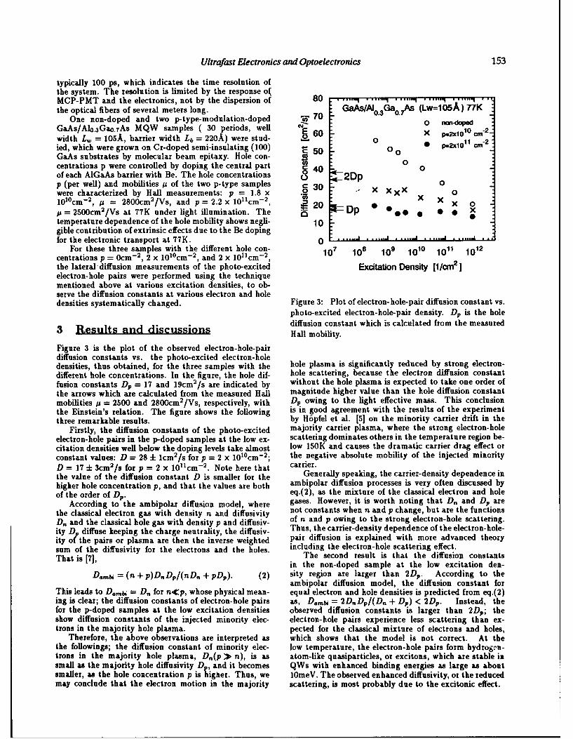
Ultrafast Electronics and Optoelectronics 153
typically 100 ps, which indicates the time resolution ofthe system. The resolution is limited by the response ofMCP-PMT and the electronics, not by the dispersion of 80 . .
the optical fibers of several meters long. GaAs/Ao.Ga0A6s (Lwf105 A)77KOne non-doped and two p-type-modulation-doped •, 70 03 0
GaAs/Alo.3Gao.7 As MQW samples ( 30 periods, well 0 fO nn-dopedwidth 4, 105osA, barrier width Lb =220A) were stud- 60 0X p.2xi010 an"2
ied, which were grown on Cr-doped semi-insulating (100) - 0 00 * 1'2x1° 1' cm'2
GaAs substrates by molecular beam epitaxy. Hole con-centrations p were controlled by doping the central part • 40 0of each AIGaAs barrier with Be. The hole concentrations O 2Dpp (per well) and mobilities/p of the two p-type samples 00were characterized by Hall measurements: p = 1.8 x .•_30. X X Xx 0
101°cm-2 , / = 2800cm 2/Vs, and p = 2.2 x 1011cm-2 , • 20 X X -c/p = 2500cm2/Vs at 77K under light illumination. The 20 •Dp * ** * * * xtemperature dependence of the hole mobility shows negli- 10gible contribution of extrinsic effects due to the Be dopingfor the electronic transport at 77K. 0........ a......a..... J .... a... .,.
For these three samples with the different hole con- 10 a0 19 10o 101 102centrations p = 0cm-2 , 2 x 10'°cm-2 , and 2 x 10 11cm-2,10 0 10 0 10 0the lateral diffusion measurements of the photo-excited Excitation Density [1/cm 2 ]electron-hole pairs were performed using the techniquementioned above at various excitation densities, to ob-serve the diffusion constants at various electron and holedensities systematically changed. Figure 3: Plot of electron-hole-pair diffusion constant vs.
photo-excited electron-hole-pair density. Dp is the holediffusion constant which is calculated from the measured
3 Results and discussions Hall mobility.
Figure 3 is the plot of the observed electron-hole-pairdiffusion constants vs. the photo-excited electron-holedensities, thus obtained, for the three sam pies with the hole plasma is significantly reduced by strong electron-different hole concentrations. In the figure, the hole dif- hole scattering, because the electron diffusion constantfusion constants Dp= 17 and 19cm 2/s are indicated by without the hole plasma is expected to take one order ofthe arrows which are calculated from the measured Hall magnitude higher value than the hole diffusion constantmobilities /p = 2500 and 2800cm 2 /Vs, respectively, with Dp owing to the light effective mass. This conclusionthe Einstein's relation. The figure shows the following is in good agreement with the results of the experimentthree remarkable results, by H~pfel et al. [5] on the minority carrier drift in the
Firstly, the diffusion constants of the photo-excited majority carrier plasma, where the strong electron-holeelectron-hole pairs in the p-doped samples at the low ex- scattering dominates others in the temperature region be-citation densities well below the doping levels take almost low 150K and causes the dramatic carrier drag effect orconstant values: D = 28 -I lcm2 /s for p = 2 x 10i°cm-2 ; the negative absolute mobility of the injected minorityD = 17 d: 3cm 2/s for p = 2 x 10' 1cm-2 . Note here that carrier.the value of the diffusion constant D is smaller for the Generally speaking, the carrier-density dependence inhigher hole concentration p, and that the values are both ambipolar diffusion processes is very often discussed byof the order of Dp. eq.(2), as the mixture of the classical electron and hole
According to the ambipolar diffusion model, where gases. However, it is worth noting that D,, and Dp arethe classical electron gas with density n and diffusivity not constants when n and p change, but are the functionsD,, and the classical hole gas with density p and diffusiv- of n and p owing to the strong electron-hole scattering.
ity Dp diffuse keeping the charge neutrality, the diffusiv- Thus, the carrier-density dependence of the electron-hole-ity ol'the pairs or plasma are then the inverse weighted pair diffusion is explained with more advanced theorysum of the diffusivity for the electrons and the holes. including the electron-hole scattering effect.
That i [7JThe second result is that the diffusion constantsThat i [7],in the non-doped sample at the low excitation den-
Damb = (n +p)DnDp/(nD,, + pDp). (2) sity region are larger than 2Dv. According to theambipolar diffusion model, the diffusion constant for
This leads to D8 ,n,• = Dn for n'c•p, whose physical mean- equal electron and hole densities is predicted from eq.(2)ing is clear; the diffusion constants of electron-hole pairs as, D.,n,,, = 2D.Dp/(D. + Dp) < 2Dp. Instead, thefor the p-doped samples at the low excitation densities observed diffusion constants is larger than 2D,; theshow diffusion constants of the injected minority elec- electron-hole pairs experience less scattering than ex-trons in the majority hole plasma. pected for the classical mixture of electrons and holes,
Therefore, the above observations are interpreted as which shows that the model is not correct. At thethe followings; the diffusion constant of minority elec- low temperature, the electron-hole pairs form hydrogen-trons in the majority hole plasma, Dn(p )1 n), is as atom-like quasiparticles, or excitons, which are stable insmall as the majority hole diffusivity Dp and it becomes QWs with enhanced binding energies as large as aboutsmaller, as the hole concentration p is hiigher. Thus, we 10meV. The observed enhanced diffusivity, or the reducedmay conclude that the electron motion in the majority scattering, is most probably due to the excitonic elfect.
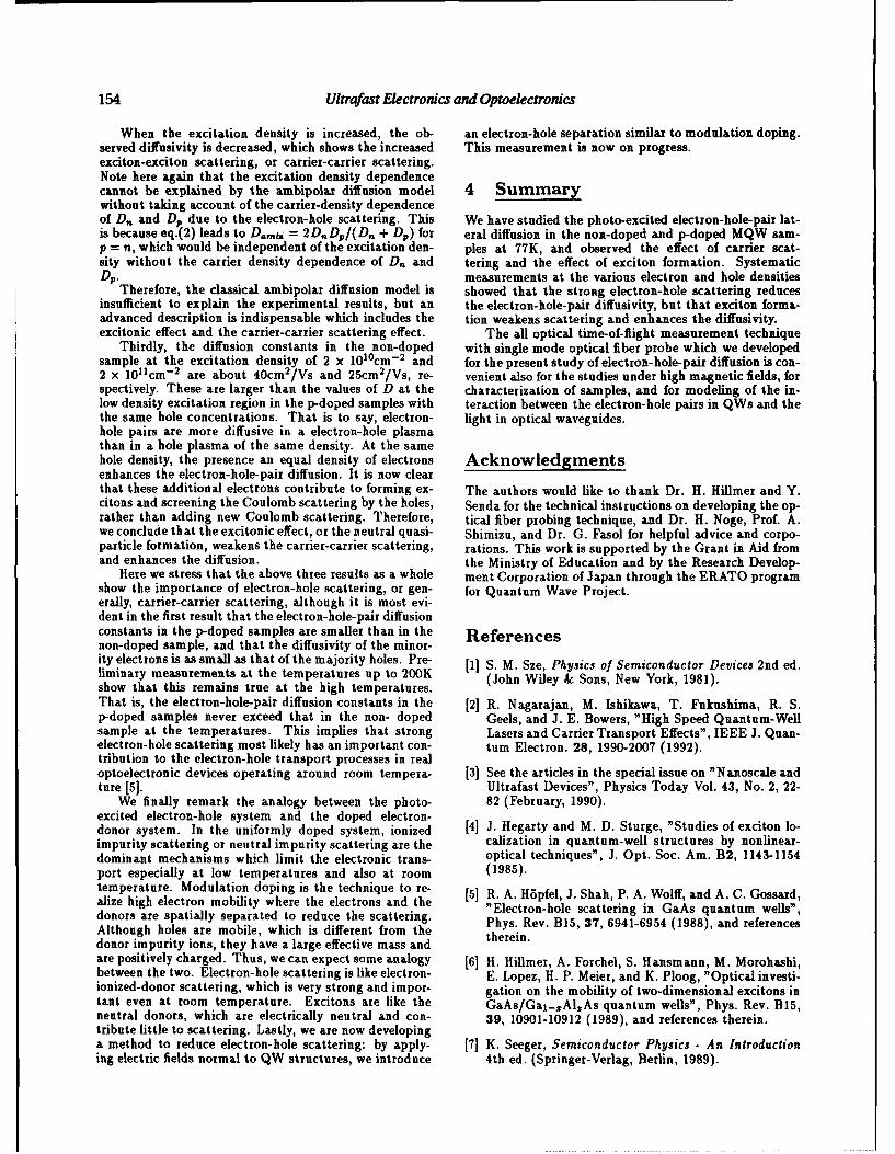
154 Ultrafast Flectronics and Optoelectronics
When the excitation density is increased, the ob- an electron-hole separation similar to modulation doping.served diffusivity is decreased, which shows the increased This measurement is now on progress.exciton-exciton scattering, or carrier-carrier scattering.Note here again that the excitation density dependencecannot be explained by the ambipolar diffusion model 4 Summarywithout taking account of the carrier-density dependenceof D,, and Dp due to the electron-hole scattering. This We have studied the photo-excited electron-hole-pair lat-is because eq.(2) leads to Do,,,b, = 2D, Dp/(D,, + Dp) for eral diffusion in the non-doped and p-doped MQW sam-p = n, which would be independent of the excitation den- pies at 77K, and observed the effect of carrier scat-sity without the carrier density dependence of D, and tering and the effect of exciton formation. SystematicDp. measurements at the various electron and hole densities
Therefore, the classical ambipolar diffusion model is showed that the strong electron-hole scattering reducesinsufficient to explain the experimental results, but an the electron-hole-pair diffusivity, but that exciton forma-advanced description is indispensable which includes the tion weakens scattering and enhances the diffusivity.excitonic effect and the carrier-carrier scattering effect. The all optical time-of-flight measurement technique
Thirdly, the diffusion constants in the non-doped with single mode optical fiber probe which we developedsample at the excitation density of 2 x 1010 cm- 2 and for the present study of electron-hole-pair diffusion is con-2 x 1011 cm- 2 are about 40cm 2/Vs and 25cm2/Vs, re- venient also for the studies under high magnetic fields, forspectively. These are larger than the values of D at the characterization of samples, and for modeling of the in-low density excitation region in the p-doped samples with teraction between the electron-hole pairs in QWs and thethe same hole concentrations. That is to say, electron- light in optical waveguides.hole pairs are more diffusive in a electron-hole plasmathan in a hole plasma of the same density. At the samehole density, the presence an equal density of electrons Acknowledgmentsenhances the electron-hole-pair diffusion. It is now clearthat these additional electrons contribute to forming ex- The authors would like to thank Dr. H. Hillmer and Y.citons and screening the Coulomb scattering by the holes, Senda for the technical instructions on developing the op-rather than adding new Coulomb scattering. Therefore, tical fiber probing technique, and Dr. H. Noge, Prof. A.we conclude that the excitonic effect, or the neutral quasi- Shimizu, and Dr. G. Fasol for helpful advice and corpo-particle formation, weakens the carrier-carrier scattering, rations. This work is supported by the Grant in Aid fromand enhances the diffusion. the Ministry of Education and by the Research Develop-
Here we stress that the above three results as a whole ment Corporation of Japan through the ERATO programshow the importance of electron-hole scattering, or gen- for Quantum Wave Project.erally, carrier-carrier scattering, although it is most evi-dent in the first result that the electron-hole-pair diffusionconstants in the p-doped samples are smaller than in the Referencesnon-doped sample, and that the diffusivity of the minor-ity electrons is as small as that of the majority holes. Pre- [1] S. M. Sze, Physics of Semiconductor Devices 2nd ed.liminary measurements at the temperatures up to 200K (John Wiley & Sons, New York, 1981).show that this remains true at the high temperatures.That is, the electron-hole-pair diffusion constants in the [2] R. Nagarajan, M. Ishikawa, T. Fukushima, R. S.p-doped samples never exceed that in the non- doped Geels, and J. E. Bowers, "High Speed Quantum-Wellsample at the temperatures. This implies that strong Lasers and Carrier Transport Effects", IEEE J. Quan-electron-hole scattering most likely has an important con- turn Electron. 28, 1990-2007 (1992).tribution to the electron-hole transport processes in realoptoelectronic devices operating around room tempera- [3] See the articles in the special issue on "Nanoscale andture [5]. Ultrafast Devices", Physics Today Vol. 43, No. 2, 22-
We finally remark the analogy between the photo- 82 (February, 1990).excited electron-hole system and the doped electron-donor system. In the uniformly doped system, ionized [4] J. Hegarty and M. D. Sturge, "Studies of exciton lo-impurity scattering or neutral impurity scattering are the calization in quantum-well structures by nonlinear-dominant mechanisms which limit the electronic trans- optical techniques", J. Opt. Soc. Am. B2, 1143-1154port especially at low temperatures and also at room (1985).temperature. Modulation doping is the technique to re- [5] R. A. H6pfel, J. Shah, P. A. Wolff, and A. C. Gossard,alize high electron mobility where the electrons and the "Electron-hole scattering in GaAs quantum wells",donors are spatially separated to reduce the scattering. Phys. Rev. BIS, 37, 6941-6954 (1988), and referencesAlthough holes are mobile, which is different from the therein.donor impurity ions, they have a large effective mass andare positively charged. Thus, we can expect some analogy [6] H. Hillmer, A. Forchel, S. Hansmann, M. Morohashi,between the two. Electron-hole scattering is like electron- E. Lopez, H. P. Meier, and K. Ploog, "Optical investi-ionized-donor scattering, which is very strong and impor- gation on the mobility of two-dimensional excitons intant even at room temperature. Excitons are like the GaAs/Gal-,,AlzAs quantum wells", Phys. Rev. B15,neutral donors, which are electrically neutral and con- 39, 10901-10912 (1989), and references therein.tribute little to scattering. Lastly, we are now developinga method to reduce electron-hole scattering: by apply- [7] K. Seeger, Semiconductor Physics - An Introductioning electric fields normal to QW structures, we introduce 4th ed. (Springer-Verlag, Berlin, 1989).

Novel Sources and Techniques
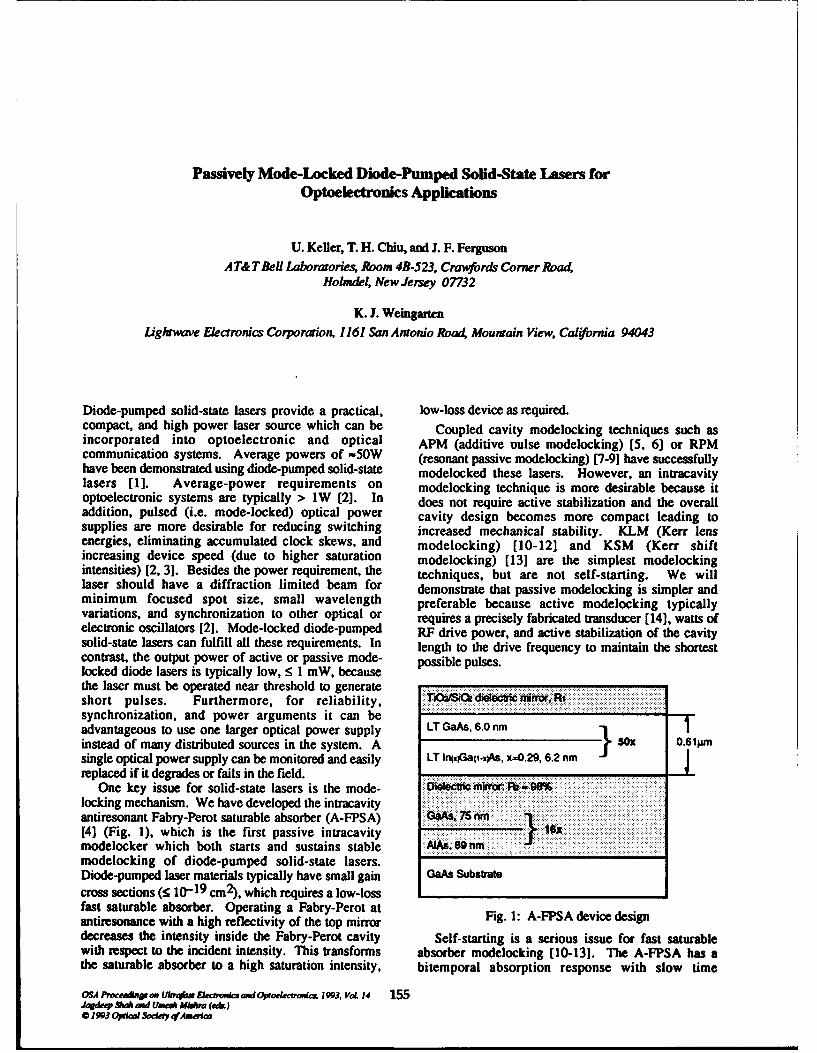
Passively Mode-Locked Diode-Pumped Solid-State Lasers forOptoelectronics Applications
U. Keller, T. H. Chiu, and J. F. Ferguson
AT& T BeU Laboratories, Room 4B-523, Crawfords Corner Roai4Holmdel, New Jersey 07732
K. J. WeingartenLightwave Electronics Corporaion, 1161 San Antonio Road Mountain View, California 94043
Diode-pumped solid-state lasers provide a practical, low-loss device as required.compact, and high power laser source which can be Coupled cavity modelocking techniques such asincorporated into optoelectronic and optical APM (additive vulse modelocking) [5, 6] or RPMcommunication systems. Average powers of -50W (resonant passive modelocking) [7-9] have successfullyhave been demonstrated using diode-pumped solid-state modelocked these lasers. However, an intracavitylasers [1]. Average-power requirements on modelocking technique is more desirable because itoptoelectronic systems are typically > IW [2]. In does not require active stabilization and the overalladdition, pulsed (i.e. mode-locked) optical power cavity design becomes more compact leading tosupplies are more desirable for reducing switching increased mechanical stability. KLM (Kerr lensenergies, eliminating accumulated clock skews, and modelocking) [10-12] and KSM (Kerr shiftincreasing device speed (due to higher saturation modelocking) [13] are the simplest modelockingintensities) [2, 3]. Besides the power requirement, the techniques, but are not self-starting. We willlaser should have a diffraction limited beam for demonstrate that passive modelocking is simpler andminimum focused spot size, small wavelength preferable because active modelocking typicallyvariations, and synchronization to other optical or requires a precisely fabricated transducer [14], watts ofelectronic oscillators [2]. Mode-locked diode-pumped RF drive power, and active stabilization of the cavitysolid-state lasers can fulfill all these requirements. In length to the drive frequency to maintain the shortestcontrast, the output power of active or passive mode- possible pulses.locked diode lasers is typically low, < I mW, becausethe laser must be operated near threshold to generateshort pulses. Furthermore, for reliability, iI dieletricmirfrl'Qrisynchronization, and power arguments it can beadvantageous to use one larger optical power supply LT GaAs, 6.0 ruminstead of many distributed sources in the system. A SOX 0.61Wnsingle optical power supply can be monitored and easily LT tlr(xGap.xAs, x-0.29, 6.2 nmreplaced if it degrades or fails in the field.
One key issue for solid-state lasers is the mode- . .... O mk': l: . . .locking mechanism. We have developed the intracavityantiresonant Fabry-Perot saturable absorber (A-FPSA) GaAs, 7...n.[4] (Fig. 1), which is the first passive intracavity laxmodelocker which both starts and sustains stable AfI, 89 nI I -modelocking of diode-pumped solid-state lasers.Diode-pumped laser materials typically have small gain GaAs Substratecross sections (5 10-19 cm2 ), which requires a low-lossfast saturable absorber. Operating a Fabry-Perot at Fig. 1: A-FPSA device designantiresonance with a high reflectivity of the top mirrordecreases the intensity inside the Fabry-Perot cavity Self-starting is a serious issue for fast saturablewith respect to the incident intensity. This transforms absorber modelocking [10-13]. The A-FPSA has athe saturable absorber to a high saturation intensity, bitemporal absorption response with slow time
OSA PfocfeaapN on Ukr4W Ekcemkd Optd ,oe hc,. 193, VoL 14 155Jqdp Mkh amd UmeA Midm (eAd)* 1993 Optical Sodoy qfAmwaz
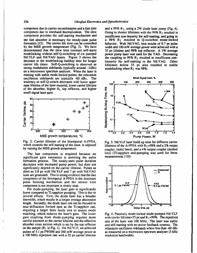
156 Ultrafast Electronics and Optoelectronics
component due to carrier recombination and a fast time and a 99% R 1 , using a 2W diode laser pump (Fig. 4).component due to intraband thermalization. The slow Going to shorter lifetimes with the 99% R1 resulted incomponent provides the self-starting mechanism and insufficient non-linearity for self-starting, and going tothe fast absorber is necessary for steady-state pulse a 98% RI resulted in Q-switched mode-lockedformation [15]. The carrier life time can be controlled behavior. With Nd:YAG, best results of 8.7 ps pulseby the MBE growth temperature (Fig. 2). We have width and 100 mW average power were achieved with ademonstrated that the slow time constant self-starts 35 ps lifetime and 98% top reflector. A IW averagemodelocking without self-Q-switching of cw pumped power pump laser was used for the YAG. DecreasingNd:YLF and Nd:YAG lasers. Figure 3 shows the the coupling to 99% R1 resulted in insufficient non-decrease in the modelocking buildup time for longer linearity for self-starting in the Nd:YAG. Othercarrier life times. Self-Q-switching is observed as lifetimes below 35 ps also resulted in stablestrong modulation sidebands (typically around -ldBc) modelocking when R1 was 98%.on a microwave spectrum analyzer. When the laser isrunning with stable mode-locked pulses, the relaxationoscillation sidebands are typically -60 dBc. The Small Signal Gain. %tendency to self-Q-switch decreases with lower upper 0 100 200 300 400 500state lifetime of the laser material, lower carrier lifetime 100 I I
of the absorber, higher R1 top reflector, and higher Esmall-signal laser gain. 6°'-
E l0
so FE
. ~0 i Ii3p
C) 0
20 5 0 5 0 .11 I I I I0.2 0.4 0.6 0.8 1.0 1.2 1.4
MBE growth temperatures, °C Pump Power, W
Fig. 2: Carrier lifetime of the bitemporal A-FPSA, Fig. 3: Nd:YLF laser build-up time for different carrierwhich controls the self-starting of the laser, is adjusted lifetimes of the A-FPSA with RI=98% and a 2% outputby varying the MBE growth temperature. coupler, (solid lines), and a 4% output coupler (dashed
The fast component is required because no line) (Ti:sapphire end-pumping was used for thesesignificant gain saturation is assisting the pulse measurements 115])formation process. The steady-state pulse durationdecreases with increased pump power, but does not 1significantly depend on the carrier lifetime. Pulses as maueshort as 2.8 ps with Nd:YLF and 7 ps with Nd:YAGlaser are generated. This is strong evidence that the fast 0.6-- i
component of the bitemporal A-FPSA is the dominantpulse forming mechanism and the slower time 0.6 L A
component is not important in steady-state. 5. sFH . sFHFor diode-pumping, the laser gain is significantly 0.,
lower compared to Ti:sapphire pumping. This is due to <several effects. First, the diode laser has a broader 0.2linewidth, which results in a longer average absorptionlength. Secondly, the diode laser can not be focused to 1 20 0
-20 200 0 0 20
near-diffraction limited spot as the Ti:sapphire can, Dlytm.prequiring a larger laser mode size to ensure mode Dlytm.Pmatching, which reduces the laser's gain. The lower Fig. 4: Passively mode-locked diode-pumped Nd:YLFgain resulting from diode-pumping requires more with carrier lifetime=35 ps and R 1 =99%. The repetitioncareful attention to the carrier lifetime and the effective rate of the laser was 100 MHz. The laser was stableabsorber cross section which is set by the top reflector and self-starting with no active feedback systems. Theon the sample (R1 in Fig. 1). For Nd: YLF, we achieved relaxation oscillation sidebands where less than -60 dBcpulses of 5.1 ps FWHM and 260 mW average power at as measured on a microwave spectrum analyzer (3 kHza 100 MHz repetition rate with a 35 ps carrier lifetime resolution bandwidth).
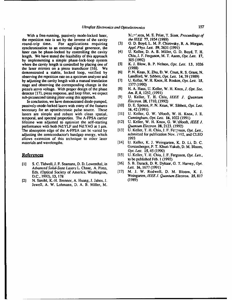
Ultrafast Electronics and Optoelectronics 157
With a free-running, passively mode-locked laser, ?v 1-rxacca, M. E. Prise, T. Sizer, Proceedings ofthe repetition rate is set by the inverse of the cavity the IEEE 77, 1954 (1989)round-trip time. For applications requiring [3] G. D. Boyd, L. M. F. Chirovsky, R. A. Morgan,synchronization to an external signal generator, the Appl. Phys. Lett. 59, 2631 (1991)laser can be phase-locked by controlling the cavity [4] U. Keller, D. A. B. Miller, G. D. Boyd, T. H.length. We have tested the feasibility of this approach Chiu, J. F. Ferguson, M. T. Asom, Opt. Lett. 17,by implementing a simple phase-lock-loop system 505 (1992)where the cavity length is controlled by placing one of [5] K. J. Blow, B. P. Nelson, Opt. Lett. 13, 1026the laser mirrors on a piezo transducer [16]. We (1988)demonstrated a stable, locked loop, verified by [61 P. N. Kean, X. Zhu, D. W. Crust, R. S. Grant, N.observing the repetition rate on a spectrum analyzer and Landford, W. Sibbett, Opt. Lett. 14,39 (1989)by adjusting the cavity length with a manual translation [7] U. Keller, W. H. Knox, H. Roskos, Opt. Lett. 15,stage and observing the corresponding change in the 1377 (1990)piezo's servo voltage. With proper design of the phase [8] H. A. Haus, U. Keller, W. H. Knox, J. Opt. Soc.detector [17], piezo response, and loop filter, we expect Am. B, 8, 1252, (1991)sub-picosecond timing jitter using this approach. [91 U. Keller, T. H. Chiu, IEEE J. Quantum
In conclusion, we have demonstrated diode-pumped, Electron. 28, 1710, (1992)passively-mode-locked lasers with many of the features [10] D. E. Spence, P. N. Kean, W. Sibbett, Opt. Lett.necessary for an optoelectronic pulse source. These 16,42 (1991)lasers are simple and robust with clean spatial, [11] U. Keller, G. W. 'tHooft, W. H. Knox, J. E.temporal, and spectral properties. The A-FPSA carrier Cunningham, Opt. Lett. 16, 1022 (1991)lifetime was adjusted to optimize the self-starting [121 U. Keller, W. H. Knox, G. W.'tHooft, IEEE J.performance with both Nd:YLF and Nd:YAG at 1 lim. Quantum Electron. 28, 2123, (1992)The absorption edge of the A-FPSA can be varied by [131 U. Keller, T. H. Chiu, J. F. Fer-lson, Opt. Lett.,adjusting the semiconductor's bandgap energy, which submitted for publication Nov. 1992, and CLEOallows extension of this technique to other laser 1993materials and wavelengths. [14] U. Keller, K. J. Weingarten, K. D. Li, D. C.
Gerstenberger, P. T. Khuri-Yakub, D. M. Bloom,Opt. Lett. 15,45 (1990)
References [15] U. Keller, T. H. Chiu, J. F. Ferguson, Opt. Lett.,to be published Feb. 1 (1992)
[1] S. C. Tidwell, J. F. Seamans, D. D. Lowenthal, in [16] S. B. Darack, D. R. Dykaar, G. T. Harvey, Opt.Advanced Solid-State Lasers L. Chase, A. Pinto, Lett. 16, 1677 (1991)Eds. (Optical Society of America, Washington, [17] M. J. W. Rodwell, D. M. Bloom, K. J.D.C., 1992), 13, 178 Weingarten, IEEE J. Quantum Electron. 25, 817
[2] N. Streibl, K.-H. Brenner, A. Huang, J. Jahns, J. (1989)Jewell, A. W. Lohmann, D. A. B. Miller, M.
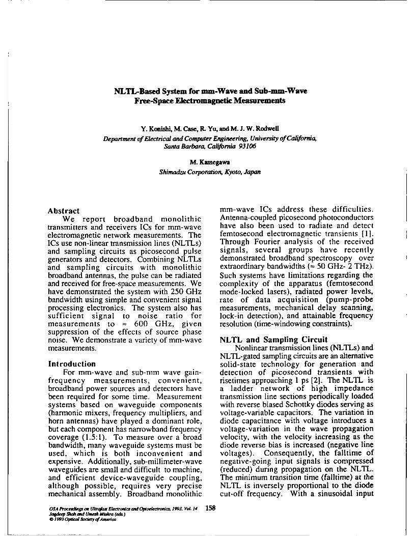
NLTL-Based System for mm-Wave and Sub-mm-WaveFree-Space Electromagnetic Measurements
Y. Koishi, M. Case, R. Yu, and M. J. W. Rodwell
Department of Electrical and Computer Engineering, University of California,Santa Barbara, California 93106
M. Kamegawa
Shimadzu Corporation, Kyoto, Japan
Abstract mm-wave ICs address these difficulties.We report broadband monolithic Antenna-coupled picosecond photoconductors
transmitters and receivers ICs for mm-wave have also been used to radiate and detectelectromagnetic network measurements. The femtosecond electromagnetic transients [1].ICs use non-linear transmission lines (NLTLs) Through Fourier analysis of the receivedand sampling circuits as picosecond pulse signals, several groups have recentlygenerators and detectors. Combining NLTLs demonstrated broadband spectroscopy overand sampling circuits with monolithic extraordinary bandwidths (= 50 GHz- 2 THz).broadband antennas, the pulse can be radiated Such systems have limitations regarding theand received for free-space measurements. We complexity of the apparatus (femtosecondhave demonstrated the system with 250 GHz mode-locked lasers), radiated power levels,bandwidth using simple and convenient signal rate of data acquisition (pump-probeprocessing electronics. The system also has measurements, mechanical delay scanning,sufficient signal to noise ratio for lock-in detection), and attainable frequencymeasurements to = 600 GHz, given resolution (time-windowing constraints).suppression of the effects of source phasenoise. We demonstrate a variety of mm-wave NLTL and Sampling Circuitmeasurements. Nonlinear transmission lines (NLTLs) and
NLTL-gated sampling circuits are an alternativeIntroduction solid-state technology for generation and
For mm-wave and sub-mm wave gain- detection of picosecond transients withfrequency measurements, convenient, risetimes approaching 1 ps [2]. The NLTL isbroadband power sources and detectors have a ladder network of high impedancebeen required for some time. Measurement transmission line sections periodically loadedsystems based on waveguide components with reverse biased Schottky diodes serving as(harmonic mixers, frequency multipliers, and voltage-variable capacitors. The variation inhorn antennas) have played a dominant role, diode capacitance with voltage introduces abut each component has narrowband frequency voltage-variation in the wave propagationcoverage (1.5:1). To measure over a broad velocity, with the velocity increasing as thebandwidth, many waveguide systems must be diode reverse bias is increased (negative lineused, which is both inconvenient and voltages). Consequently, the falltime ofexpensive. Additionally, sub-millimeter-wave negative-going input signals is compressedwaveguides are small and difficult to machine, (reduced) during propagation on the NLTL.and efficient device-waveguide coupling, The minimum transition time (falltime) at thealthough possible, requires very precise NLTL is inversely proportional to the diodemechanical assembly. Broadband monolithic cut-off frequency. With a sinusoidal input
OSA Procea*np on nia'*.w Eacro"a Optoelkctnwi.= 1993, Vol. 14 158J.,deep 9aa and Umuf, Mbhm (ak)01993 Opdca1 Sode1y efAnwic
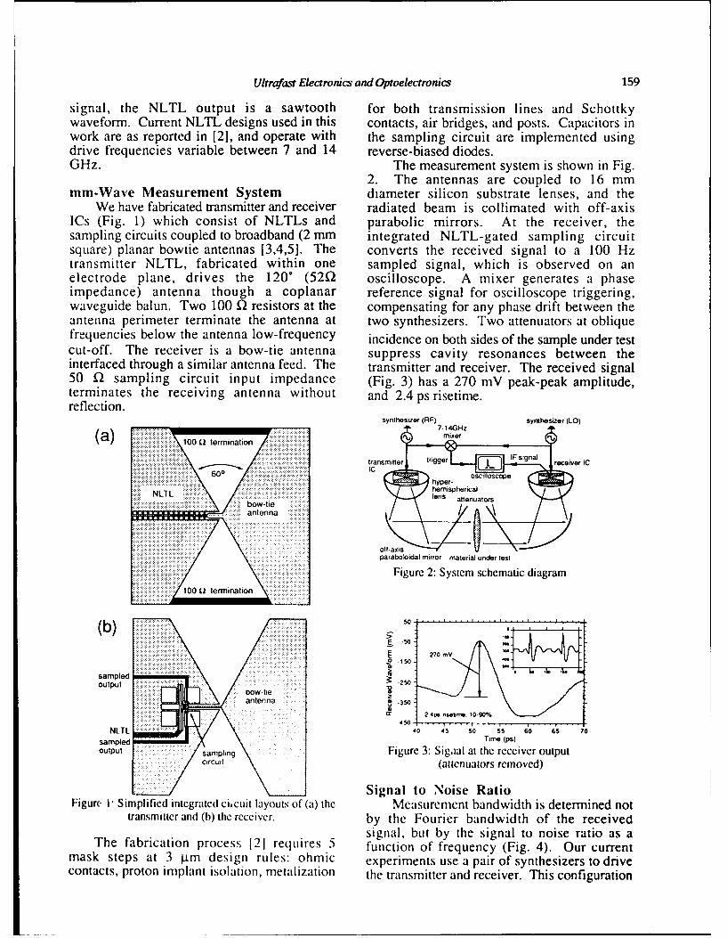
Ultrafast Electronics and Optoelectronics 159
signal, the NLTL output is a sawtooth for both transmission lines and Schottkywaveform. Current NLTL designs used in this contacts, air bridges, and posts. Capacitors inwork are as reported in [21, and operate with the sampling circuit are implemented usingdrive frequencies variable between 7 and 14 reverse-biased diodes.GHz. The measurement system is shown in Fig.
2. The antennas are coupled to 16 mmmm-Wave Measurement System diameter silicon substrate lenses, and the
We have fabricated transmitter and receiver radiated beam is collimated with off-axisICs (Fig. 1) which consist of NLTLs and parabolic mirrors. At the receiver, thesampling circuits coupled to broadband (2 mm integrated NLTL-gated sampling circuitsquare) planar bowtie antennas [3,4,5]. The converts the received signal to a 100 Hztransmitter NLTL, fabricated within one sampled signal, which is observed on anelectrode plane, drives the 120" (520 oscilloscope. A mixer generates a phaseimpedance) antenna though a coplanar reference signal for oscilloscope triggering,waveguide balun. Two 100 Q resistors at the compensating for any phase drift between theantenna perimeter terminate the antenna at two synthesizers. Two attenuators at obliquefrequencies below the antenna low-frequency incidence on both sides of the sample under testcut-off. The receiver is a bow-tie antenna suppress cavity resonances between theinterfaced through a similar antenna feed. The transmitter and receiver. The received signal50 Q sampling circuit input impedance (Fig. 3) has a 270 mV peak-peak amplitude,terminates the receiving antenna without and 2.4 ps risetime.reflection.
synthesizer (RFI) synthesizer (LO)
(a mixer~iii ~ii e(ac100 Q termination
transm ittler trigger [~ J IF signal re ivrI...... 600 Icl scp
. ......... 0 m
S~~~~~bowte" '._
. antn a i -3
.... . . ... :"".......s tme 1 -9 W
hyapoia iro aeria- nerts
Fiue2:Ssemishemiatiliga
SL 1 lermu a atoenuatorsn-- -- -- - I ' a te n
250
S,___ Sina to s Nisen. Ratio.
.450
270 M5V 5 0 5 7
Tim tieL
output sapigFigure 3: Sigaal at the receiver outputcircuit(attenuators removed)
Signal to Noise RatioFigurc P" Simplified integrated cicuit layouts of (a) the Measurement bandwidth is determined not
transmitter and (b) the receiver, by the Fourier bandwidth of the receivedsignal, but by the signal to noise ratio as a
The fabrication process 121 requires 5 function of frequency (Fig. 4). Our currentmask steps at 3 pim design rules: ohmic experiments use a pair of synthesizers to drivecontacts, proton implant isolation, nietalization the transmitter and receiver. This configuration
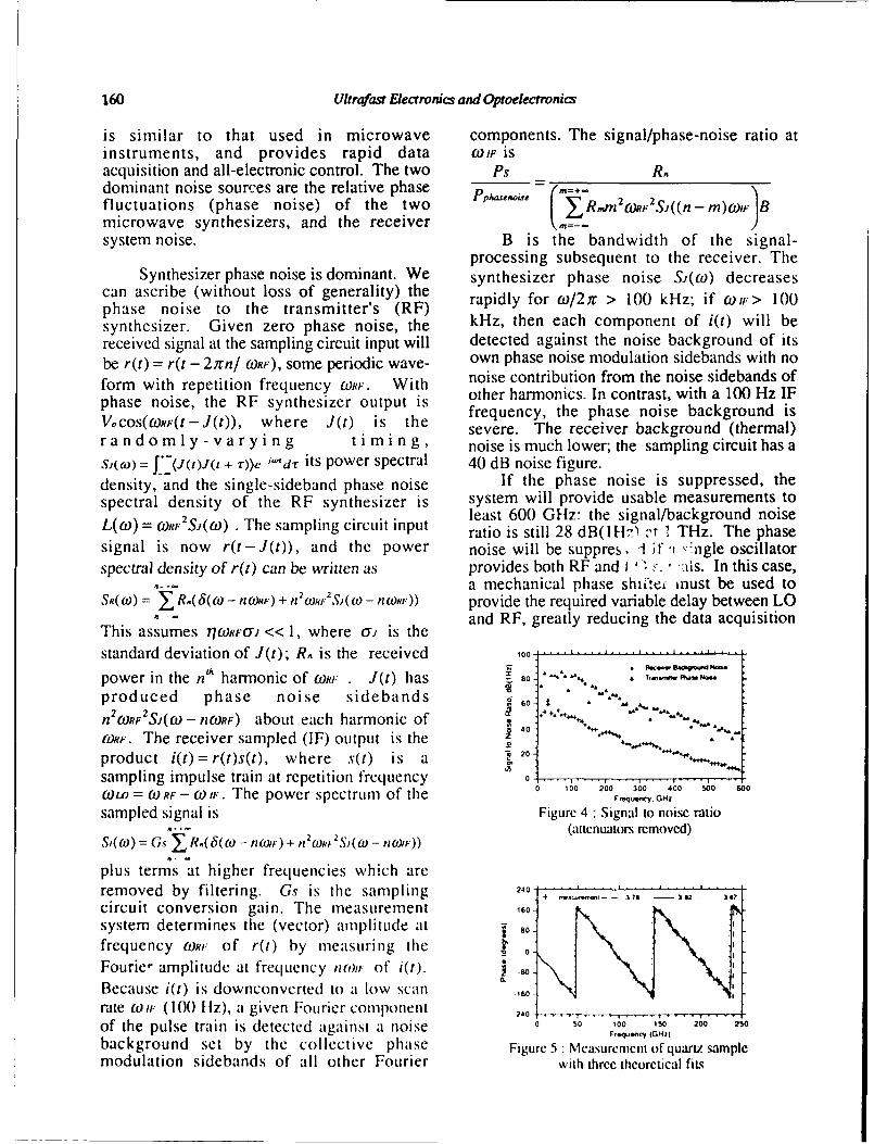
160 Ultrafast Electronics and Optoelectronics
is similar to that used in microwave components. The signal/phase-noise ratio atinstruments, and provides rapid data tOJI isacquisition and all-electronic control. The two Ps R.dominant noise sources are the relative phase ,,-,(M-fluctuations (phase noise) of the two I R,,dn 2W"RF 2SJ((n - m) owF Bmicrowave synthesizers, and the receiver .=_Dsystem noise. B is the bandwidth of the signal-
processing subsequent to the receiver. TheSynthesizer phase noise is dominant. We synthesizer phase noise S,(to) decreases
can ascribe (without loss of generality) the rapidly for ol21r > 100 kHz; if cojF> 100phase noise to the transmitter's (RF)synthesizer. Given zero phase noise, the kHz, then each component of i(t) will bereceived signal at the sampling circuit input will detected against the noise background of itsbe r(t) = r(t - 2;rn/ (ORE), some periodic wave- own phase noise modulation sidebands with no
form with repetition frequency (ORbr. With noise contribution from the noise sidebands of
phase noise, the RF synthesizer output is other harmonics. In contrast, with a 100 Hz IF
Vcos(oRF(t-J(t)), where J(t) is the frequency, the phase noise background ism nsevere. The receiver background (thermal)
randomIy -varying timing, noise is much lower; the sampling circuit has asj((O) = J •(J(t)J(t + T))e 1-d, its power spectral 40 dB noise figure.density, and the single-sideband phase noise If the phase noise is suppressed, thespectral density of the RF synthesizer is system will provide usable measurements to
L(w) = ORF 2SJO) . The sampling circuit input least 600 GHz" the signal/background noise
ratio is still 28 dB(1H7) -t I THz. The phasesignal is now r(t-J(t)), and the power noise will be suppres,. I ir'i ItQngle oscillatorspectral density of r(t) can be written as provides both RF and J 'I s_., -i is. In this case,
*...a mechanical phase shiite, mnust be used toSR(w) = R.(35(w - noft,) + nfol ,.(Sj(o) - nwRi.)) provide the required variable delay between LO
"and RF, greatly reducing the data acquisitionThis assumes 7/OJRFUrJ << , where -g is thestandard deviation of J(t); R. is the received 100power in the n"' harmonic of (ORF . J(t) has ao. +0 ,-".- ,-
produced phase noise sidebands 60 S " "n2 (Oe- - -nOF) about each harmonic of
tRon. The receiver sampled (IF) output is theproduct i(t) = r(t)s(t), where s(t) is a 2 -++
sampling impulse train at repetition frequency 0 00 100 200 300 400 Soo 600
(OU) = 0) RF - WoIF. The power spectrum of the Fm.,,y GH4
sampled signal is Figure 4 " Signal to noise ratio) (attenuators removed)S,(wo) = (s y•R(5o - nw/) + n2 2(o',.Si( C - n•)
plus terms at higher frequencies which areremoved by filtering. Gs is the sampling 240]+ 3 79 3 -2----circuit conversion gain. The measurement ,60.system determines the (vector) amplitude at 80 1
frequency (oR. of r(t) by measuring the 0 ,Fourie" amplitude at frequency n(o' of i(t). -Because i(t) is downconverted to a low scan .60rate (o. (I() Hz), a given Fourier component .240of the pulse train is detected against a noise 0 50 ,00 , 5 200 250
background set by the collective phase Figure 5: Measurement of quartz samplemodulation sidebands of all other Fourier with three theoretical fits
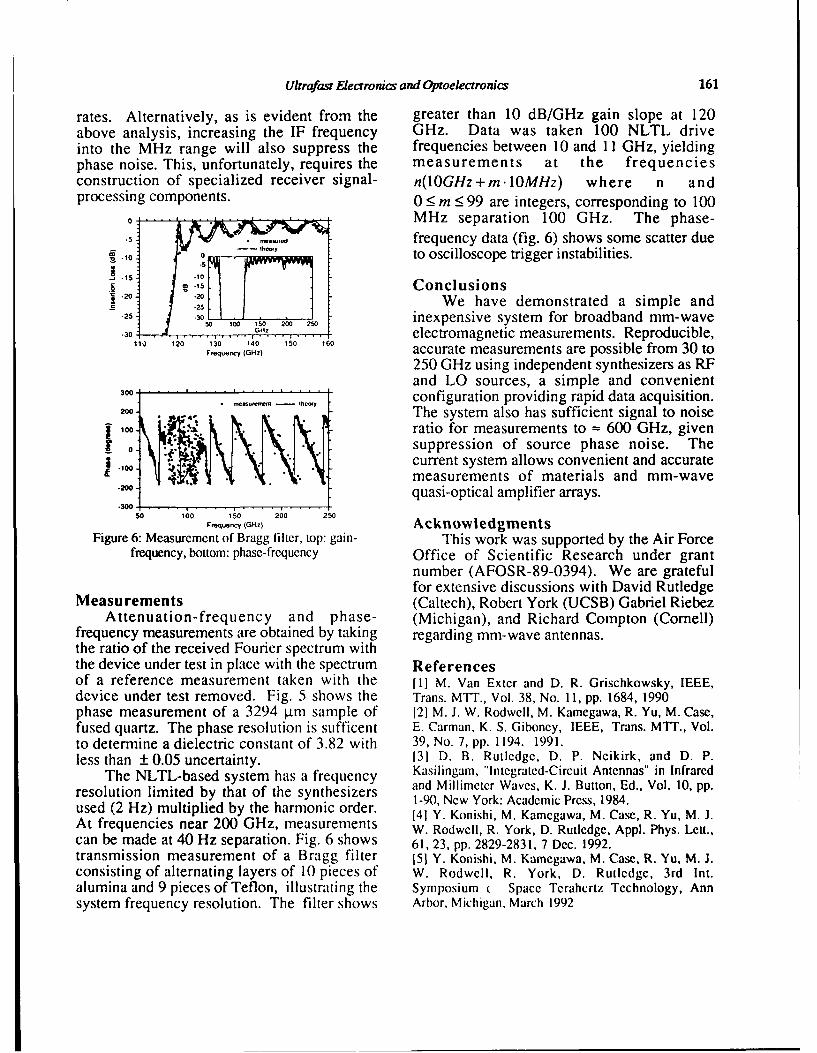
Ultrafast Electromnics and Optoelectronics 161
rates. Alternatively, as is evident from the greater than 10 dB/GHz gain slope at 120above analysis, increasing the IF frequency GHz. Data was taken 100 NLTL driveinto the MHz range will also suppress the frequencies between 10 and 11 GHz, yieldingphase noise. This, unfortunately, requires the measurements at the frequenciesconstruction of specialized receiver signal- n(lOGHz+m.lOMHz) where n andprocessing components. 0 < m < 99 are integers, corresponding to 100
0 MHz separation 100 GHz. The phase-.-5 .. frequency data (fig. 6) shows some scatter due
W .,0 to oscilloscope trigger instabilities..5S-15 -10
45.s ConclusionsS..We have demonstrated a simple and_5 -25
.25 .2 inexpensive system for broadband mm-wave,30 . 130 GH7 electromagnetic measurements. Reproducible,
110 120 130 140 1;0 160Fr,•q.ny (Gz) accurate measurements are possible from 30 to
250 GHz using independent synthesizers as RFand LO sources, a simple and convenient
300.. configuration providing rapid data acquisition.20o. The system also has sufficient signal to noise100- _. * :" *1[- •ratio for measurements to 600 GHz, given
Ssuppression of source phase noise. Thecurrent system allows convenient and accuratemeasurements of materials and mm-wave
-2W :quasi-optical amplifier arrays.50 100 150 200 250
Fmeq• y (Gz AcknowledgmentsFigure 6: Measurement of Bragg filter, top: gain- This work was supported by the Air Force
frequency, bottom: phase-frequency Office of Scientific Research under grantnumber (AFOSR-89-0394). We are gratefulfor extensive discussions with David Rutledge
Measurements (Caltech), Robert York (UCSB) Gabriel RiebezAttenuation-frequency and phase- (Michigan), and Richard Compton (Cornell)
frequency measurements are obtained by taking regarding mm-wave antennas.the ratio of the received Fourier spectrum withthe device under test in place with the spectrum Referencesof a reference measurement taken with the [1] M. Van Exter and D. R. Grischkowsky, IEEE,device under test removed. Fig. 5 shows the Trans. MTT., Vol. 38, No. 11, pp. 1684, 1990phase measurement of a 3294 -tni sample of [2] M. J. W. Rodwell, M. Kamegawa, R. Yu, M. Case,fused quartz. The phase resolution is sufficent E. Carman, K. S. Giboney, IEEE, Trans. MIT., Vol.to determine a dielectric constant of 3.82 with 39, No. 7, pp. 1194. 1991.less than ± 0.05 uncertainty. [31 D. B. Rutledge, D. P. Neikirk, and D. P.
The NLTL-based system has a frequency Kasilingam, "lntegratcd-Circuit Antennas" in Infraredresolution limited by that of the synthesizers and Millimeter Waves, K. J. Button, Ed., Vol. 10, pp.
used (2 Hz) multiplied by the harmonic order. 1-90, New York: Academic Press, 1984.[41 Y. Konishi, M. Kamegawa, M. Case, R. Yu, M. J.
At frequencies near 200 GHz, meastirements W. Rodwell, R. York, D. Rutledge, Appl. Phys. Leu.,can be made at 40 Hz separation. Fig. 6 shows 61, 23, pp. 2829-2831, 7 Dec. 1992.transmission measurement of a Bragg filter 151 Y. Konishi, M. Kamegawa, M. Case, R. Yu, M. J.consisting of alternating layers of 10 pieces of W. Rodwell, R. York, D. Rutledge, 3rd Int.alumina and 9 pieces of Teflon, illustrating the Symposium ( Space Terahcrtz Technology, Annsystem frequency resolution. The filter shows Arbor, Michigan, March 1992
Uitrafast Scanning Microscopy
S. Weiss, D. Botkdn, and D. S. Chemla
Materials Sciences Divsion, MS 2-300, Lawrence Berkeley Laboratory,Berkeley, Calijbrnia 94720
Abstract Microscope (SFM) 131 and the Near-field ScanningWe propose to combine ultrafast optical techniques Optical Microscope (NSOM) 141 have revolutionizedwith scanning probe microscopies to obtain, the field of surface science. In the scanningsimultaneously, unprecedented temporal and spatial- microscopies an atomically sharp tip (or a very smallresolution. aperture for the NSOM) is scanned very close to the
surface of a sample. Due to the close proximity of thetip to the sample, different interactions or coupling
Introduction mechanisms can occur (tunneling current, atomicVery high spatial resolution is required for forces, evanescent wave coupling). The strength ofinvestigating the phenomena that govern the physics of these interactions is a very nonlinear function of the tipmesoscopic systems and for characterizing the height. This nonlinearity provides the means foroperation of submicron optoelectronics devices. For atomic-scale control of the distance to the sample andexample, processes such as: i) carrier transport in allows high lateral resolution limited by the sharpnessmesoscopic semiconductor structures; ii) electric field of the tip. In STM, the image, obtained by collectingand voltage wave front propagation at metal- the tunneling current while scanning the tip, reflectssemiconductor interfaces; iii) light emission in the density of states of the electrons at the Fermi level
mconfined structures; all experience significant close to the surface. In SFM, the image is obtained byvariations over length scales much smaller than tmm. measuring the minute deflection of the cantilevervariatnse ovther largengthscaes much saerithatio n 1t. holding the tip, caused by the force exerted on theBecause of the large velocities of excitations in the latter by the sample (electrostatic and magnetostaticmaterials (electronic velocity in semiconductors and forces, inter-atomic forces, van der Waals forces etc.).metals is on the order of - I to 10,A/fs; voltage wave The NSOM image is obtained by evanescent fieldfronts propagate on high speed transmission lines at coupling to a sub-wavelength aperture. Presently,velocities on the order of,- 1000,A/fs), the time scale of however, the time-resolution of the scanning
their dynamics is well in the sub-picosecond domain. microscopies is limited by the scanning rate and the
Therefore, in order to understand better the data acquisition electronics.
mechanisms governing mesoscopic systems andoptimize the devices that use them, it is necessary to We propose to exploit the nonlinear nature of thcdevelop new experimental techniques with different tip-sample interactions to obtain ultrafastsimultaneous subpicosecond-time resolution and time-resolution in scanning microscopy. Thissubmicron-space resolutions, nonlinearity can be intrinsic to the nature of tip-sample
In the last decade, powerful scanning microscopy coupling or can be artificially produced by mano-techniques which can achieve atomic resolution have fabrication of custom designed tips. The timebeen developed. The invention of the Scanning resolution is achieved by modulating both the sampleTunneling Microscope (STM) [21, the Scanning Force and the tip responses with two short optical pulses, as
OSA hWCaa*np oR LP £ croftVia pt0taokcaw 1993. VoL 14 162JqpdeSp AMad UeA• MEghm (,vk)* 1993 Otdcafl &SttqfAmeao
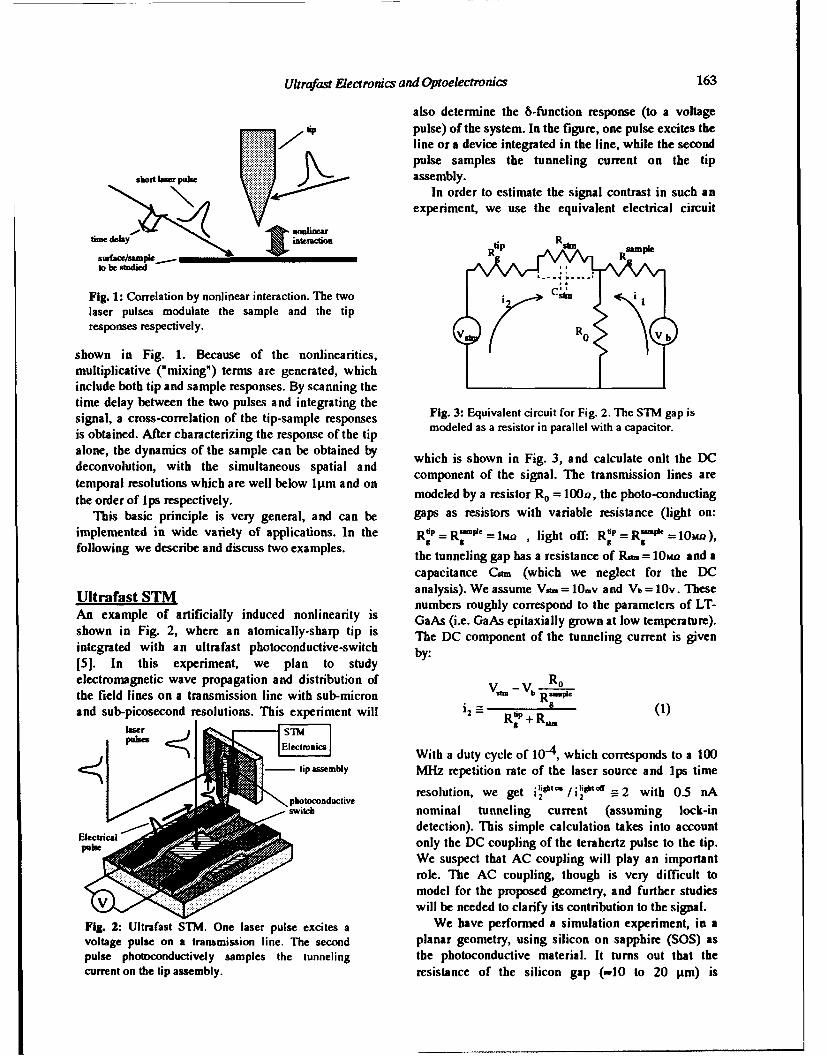
Ultrafast Electronics and Optoelectronics 163
also determine the &-function response (to a voltagetip pulse) of the system. In the figure, one pulse excites the
line or a device integrated in the line, while the secondpulse samples the tunneling current on the tip
short Inr pulse, assembly.In order to estimate the signal contrast in such an
experiment, we use the equivalent electrical circuit
to be sRtdied
Fig. 1: Correlation by nonlinear interaction. The twolaser pulses modulate the sample and the tipresponses respectively. r R
shown in Fig. 1. Because of the nonlinearities,multiplicative ("mixing") terms are generated, whichinclude both tip and sample responses. By scanning thetime delay between the two pulses and integrating thesignal, a cross-correlation of the tip-sample responses Fig. 3: Equivalent circuit for Fig. 2. The STM gap is
signl, crss-crreatin ofthetipsampe rsposesmodeled as a resistor in parallel with a capacitor.is obtained. After characterizing the response of the tipalone, the dynamics of the sample can be obtained by which is shown in Fig. 3, and calculate onlt the DCdeconvolution, with the simultaneous spatial and component of the signal. The transmission lines aretemporal resolutions which are well below ltm and on monen o thesignal.=The transhossiondlinethe order of lps respectively, modeled by a resistor R0 = 1001, the photo-conducting
This basic principle is very general, and can be gaps as resistors with variable resistance (light on:
implemented in wide variety of applications. In the RbP = R-P'c = lIa , light off: R"P= R'•€ = 10bw),
following we describe and discuss two examples. the tunneling gap has a resistance of R = 10kw and a
capacitance Cstm (which we neglect for the DC
Ultrafast STM analysis). We assume Va.= 10.v and Vb = 10v. Thesenumbers roughly correspond to the parameters of LT-
Ahowninexampleofhart anatcally-induced searptity is GaAs (i.e. GaAs epitaxially grown at low temperature).shown in Fig. 2, where an atomically-sharp tip is The DC component of the tunneling current is given
integrated with an ultrafast photoconductive-switch byc
[5). In this experiment, we plan to study by:
electromagnetic wave propagation and distribution of R0the field lines on a transmission line with sub-micron V. - Vb Rb ,kand sub-picosecond resolutions. This experiment will i2 - R 9P+ R -, (1)
StiWith a duty cycle of 10"4, which corresponds to a 100
-- tip assembly MHz repetition rate of the laser source and Ips time
photdcotd e resolution, we get il'O'/i" --2 with 0.5 nA
switch nominal tunneling current (assuming lock-inElectrical' detection). This simple calculation takes into account
Saonly the DC coupling of the terahertz pulse to the tip.We suspect that AC coupling will play an importantrole. The AC coupling, though is very difficult tomodel for the proposed geometry, and further studieswill be needed to clarify its contribution to the signal.
Fig. 2: Ultrafast STM. One laser pulse excites a We have performed a simulation experiment, in avoltage pulse on a transmission line. The second planar geometry, using silicon on sapphire (SOS) aspulse photoconductively samples the tunneling the photoconductive material. It turns out that thecurrent on the tip assembly. resistance of the silicon gap (-10 to 20 jtm) is
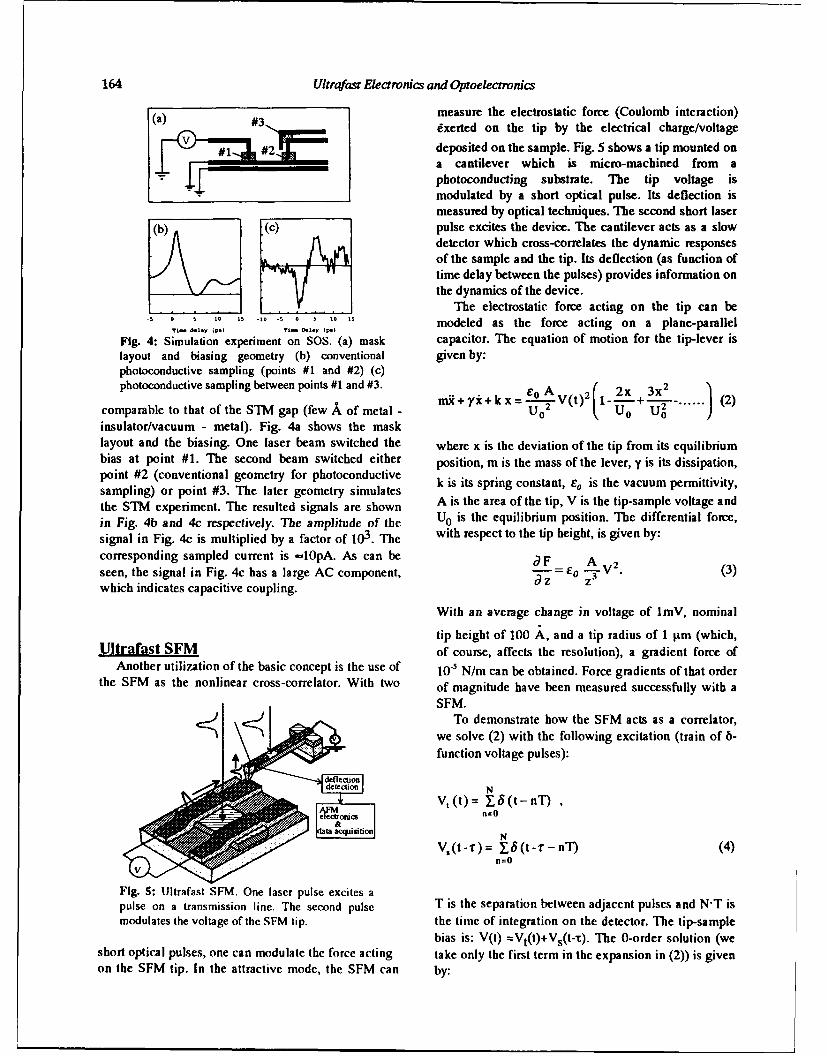
164 Ultrafast Electronics and Optoelectronics
(a) measure the electrostatic force (Coulomb interaction)(xerted on the tip by the electrical charge/voltage
S##21 deposited on the sample. Fig. 5 shows a tip mounted ona cantilever which is micro-machined from aphotoconducting substrate. The tip voltage ismodulated by a short optical pulse. Its deflection ismeasured by optical techniques. The second short laser
(b) W(c pulse excites the device. The cantilever acts as a slow7 7 2 .detector which cross-correlates the dynamic responsesof the sample and the tip. Its deflection (as function oftime delay between the pulses) provides information onthe dynamics of the device.
1 The electrostatic force acting on the tip can be-... ... is ............ i modeled as the force acting on a plane-parallelTil- ""y ip.) Ti- Delay 1P.)
Fig. 4: Simulation experiment on SOS. (a) mask capacitor. The equation of motion for the tip-lever islayout and biasing geometry (b) conventional given by:photoconductive sampling (points #1 and #2) (c)photoconductive sampling between points #1 and #3. 2 2n + Y X+ k x = co A V(t)2 I1 2x +3x .... 2
comparable to that of the STM gap (few A of metal - U0" 2 , "koo 1-2-"........(2)
insulator/vacuum - metal). Fig. 4a shows the masklayout and the biasing. One laser beam switched the where x is the deviation of the tip from its equilibriumbias at point #1. The second beam switched either position, m is the mass of the lever, y is its dissipation,point #2 (conventional geometry for photoconductivesampling) or point #3. The later geometry simulates k is its spring constant, eV is the vacuum permittivity,the STM experiment. The resulted signals are shown A is the area of the tip, V is the tip-sample voltage andin Fig. 4b and 4c respectively. The amplitude of the U0 is the equilibrium position. The differential force,signal in Fig. 4c is multiplied by a factor of 103. The with respect to the tip height, is given by:corresponding sampled current is -10pA. As can be dF- AAV2.seen, the signal in Fig. 4c has a large AC component, d z E (3)which indicates capacitive coupling.
With an average change in voltage of lmV, nominal
tip height of 100 Ak, and a tip radius of 1 g&m (which,Ultrarast SFM of course, affects the resolution), a gradient force of
Another utilization of the basic concept is the use of 1O5 N/m can be obtained. Force gradients of that orderthe SFM as the nonlinear cross-correlator. With two of magnitude have been measured successfully with a
SFM.To demonstrate how the SFM acts as a correlator,
we solve (2) with the following excitation (train of 6-I function voltage pulses):
S~~efletonic :
det c iitionNi ~ ~~~~V,(-r=,_, (t-) nT)(4o=0
N
n=O
Fig. 5: UIltrafast SFM. One laser pulse excites apulse on a transmission line. The second pulse T is the separation between adjacent pulses and N'T ismodulates the voltage of the SFM tip. the time of integration on the detector. The tip-sample
bias is: V(t) =Vt(t)+Vs(t--r). The 0-order solution (weshort optical pulses, one can modulate the force acting take only the first term in the expansion in (2)) is givenon the SFM tip. In the attractive mode, the SFM can by:
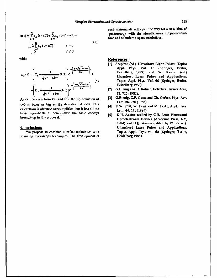
Ultrafas Electronics and Optoelectronics 165
such instruments will open the way for a new kind ofN N spectroscopy with the simultaneous subpicosecond-
) =0 t =0 time and submicron-space resolutions.
(5)+2 7 x(t- nT) T=0
n=O0- r0
with: References:[1] Shapiro: (ed.) Ultrashort Light Pubes, Topics
/_v+4 t~ Appl. Phys. Vol. 18 (Springer, Berlin,xJ(t)= CO(t) e• 2m ) + Heidelberg 1977), and W. Kaiser (ed.)J =Ultrashort Laser Pulses and Applications,
(6) Topics Appl. Phys. Vol. 60 (Springer, Berlin,
4 2m Heidelberg 1988).e(t) 41 [21 G.Binmig and H. Rohrer, Helvetica Physica Acta,
+(C r2 + ~ -4 kmý tJei_ 55, 726 (1982).As can be seen from (5) and (6), the tip deviation at [3] G.Binnig, C.F. Quate and Ch. Gerber, Phys. Rev.
x-0 is twice as big as the deviation at xruO. This Lett., 56, 930 (1986).
calculation is ofcourse oversimplified, but it has all the [41 D.W. Pohl, W. Denk and M. Lantz, Appl. Phys.
basic ingredients to demonstrate the basic concept Left., 44, 651 (1984).
brought-up in this proposal. 151 D.H. Auston (edited by C.H. Lee): PicosecondOptoelectronic Devices (Academic Press, NY,1984) and D.H. Auston (edited by W. Kaiser):
Conclusions Ultrashort Laser Pulses and Applications,We propose to combine ultrafast techniques with Topics Appl. Phys. vol. 60 (Springer, Berlin,
scanning microscopy techniques. The development of Heidelberg 1988).
Picosecond Electrical Sampling Using a Scanning ForceMicroscope
A. S. Hou, F. Ho, and D. M. Bloom
Edward L Ginzton Laboratory, Box #2, Stanford University, Stanfor4 California 94305
Abstract frequency. In the following sections, we describe themethod of operation and show preliminary results.
We demonstrate a scanning force microscope probe formeasuring ultrafast voltage signals. Equivalent-timesampling using 100 ps pulses and mixing up to 20 GHz Lsr Positionhave been achieved. Pulse Generator
Introduction %,-"To Pre-amplifier
High-speed characterization of nano-scale devices aposes a significant challenge. Presently, no onemeasurement technique simultaneously addresses therequirements of ultra-high speed and ultra-small scale.4High-SpeedOn-wafer microwave probes have been demonstrated I Circuitwith subpicosecond performance,1 but they require a vs(x~y,t)minimum contact pad area on the order of 10 microns.The bandwidth of an optical sampling system canexceed 1 THz; however, the lateral resolution is limited Iby the laser beam diameter, usually 2 to 3 microns. I.Although electron beams can yield high resolution,such systems operate in vacuum and are significantlyslower, with beam-blanking times limited by space- Figure 1. High-speed SFM electrical sampling systemcharge effects.
We present a new ultrafast technique, based Theory of Operationon the scanning force microscope (SFM), thattheoretically is sensitive enough to map an electric A scanning force microcope operates by sensing thepotential profile with better than 1 picosecond time minute deflection of a cantilever to which is attachedresolution and submicron lateral resolution. It is an an atomically sharp tip. There are two modes ofnon-invasive technique which does not require operation. In a contact SFM mode, very short-rangevacuum. Unlike past capacitance and potentiometry repulsive forces dominate and deflect the tip andmeasurements using an SFM 2-4, which were limited cantilever to allow the determination of surfaceby the slow mechanical response of the force-sensing topography. In non-contact SFM, longer range forcescantilever and feedback electronics, we avoid this (such as an attractive electric force) can cause theproblem by using the square-law force interaction cantilever to bend.present between the SFM and sample for mixing and Suppose that in non-contact mode, a voltage Vsampling. The high-speed signal under test is is present between a conductive SFM tip and thedownconverted to a much lower intermediate sample device. There will then be an attractive force F
OSA APmxes&V on LMr11 Ekc and OP,9,CWdfr oe,, 193.. VoL 14 166Jq.kq Sk* ,ad UueA MEadn (*k)* 1903 Optcal Sodeuv4F~v~imeaz
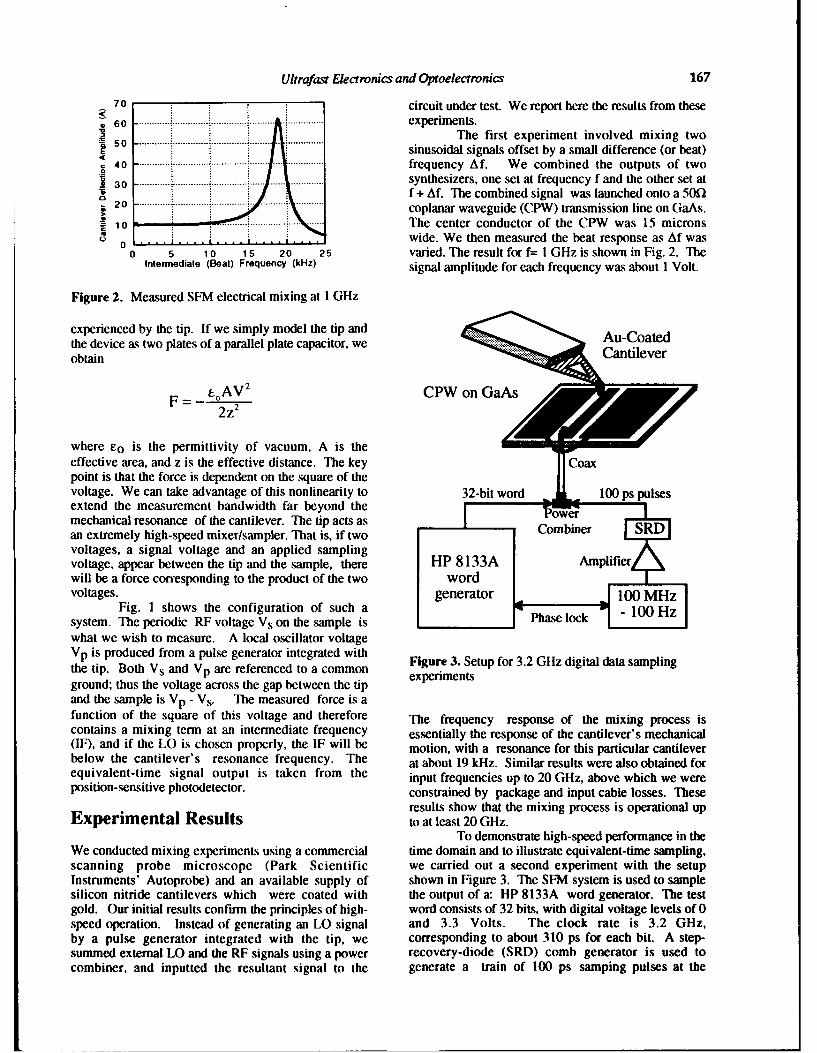
Ultrafast Electronics and Optoelecrronics 167
70 - circuit under test. We report here the results from these
60 .................. .............. .............. ............ experiments.The first experiment involved mixing two
sinusoidal signals offset by a small difference (or beat)40 frequency Af. We combined the outputs of two
30 synthesizers, one set at frequency f and the other set atf + Af. The combined signal was launched onto a 50(0
S20 coplanar waveguide (CPW) transmission line on GaAs.
S10 . ......................... .. The center conductor of the CPW was 15 micronso 0 .. .. . ... . wide. We then measured the beat response as Af was
0 5 10 15 20 25 varied. The result for f= I GHz is shown in Fig. 2. TheIntermediate (Beat) Frequency (kHz) signal amplitude for each frequency was about I Volt.
Figure 2. Measured SFM electrical mixing at 1 GHz
experienced by the tip. If we simply model the tip andthe device as two plates of a parallel plate capacitor, weobtain Cantilever
F= LoAV2 CPWonGaAs2 Z2
where Eo is the permittivity of vacuum, A is theeffective area, and z is the effective distance. The key oaxpoint is that the force is dependent on the square of thevoltage. We can take advantage of this nonlinearity to 32-bit word 100 ps pulsesextend the measurement bandwidth far beyond the [wer Imechanical resonance of the cantilever. The tip acts as Can extremely high-speed mixerlsampler. That is, if two Combiner SR
voltages, a signal voltage and an applied samplingvoltage, appear between the tip and the sample, there HP 8133A Amplifierwill be a force corresponding to the product of the two wordvoltages. generator
Fig. I shows the configuration of such a - 100 Hzsystem. The periodic RF voltage Vs on the sample is Phase ockwhat we wish to measure. A local oscillator voltageVP is produced from a pulse generator integrated with Figure 3. Setup for 3.2 GHz digital data samplingthe tip. Both Vs and Vp are referenced to a common experimentsground; thus the voltage across the gap between the tipand the sample is Vp - Vs. The measured force is afunction of the square of this voltage and therefore The frequency response of the mixing process iscontains a mixing term at an intermediate frequency essentially the response of the cantilever's mechanical(IF), and if the LO is chosen properly, the IF will be motion, with a resonance for this particular cantileverbelow the cantilever's resonance frequency. The at about 19 kHz. Similar results were also obtained forequivalent-time signal output is taken from the input frequencies up to 20 GHz, above which we wereposition-sensitive photodetector. constrained by package and input cable losses. These
results show that the mixing process is operational upExperimental Results to at least 20 GHz.
To demonstrate high-speed performance in theWe conducted mixing experiments using a commercial time domain and to illustrate equivalent-time sampling,scanning probe microscope (Park Scientific we carried out a second experiment with the setupInstruments' Autoprobe) and an available supply of shown in Figure 3. The SFM system is used to samplesilicon nitride cantilevers which were coated with the output of a: HP 8133A word generator. The testgold. Our initial results confirm the principles of high- word consists of 32 bits, with digital voltage levels of 0speed operation. Instead of generating an LO signal and 3.3 Volts. The clock rate is 3.2 GHz,by a pulse generator integrated with the tip, we corresponding to about 310 ps for each bit. A step-summed external LO and the RF signals using a power recovery-diode (SRD) comb generator is used tocombiner, and inputted the resultant signal to the generate a train of 100 ps samping pulses at the
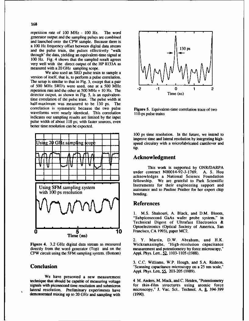
168
repetition rate of 100 MHz - 100 Hz. The wordgenerator output and the sampling pulses are combinedand launched onto the CPW sample. Because there isa 100 Hz frequency offset between digital data stream 130 psand the pulse train, the pulses effectively "walk 13pthrough" the data, yielding an equivalent-time signal at100 Hz. Fig. 4 shows that the sampled result agreesvery well with the direct output of the HP 8133A asmeasured with a 20 GHz sampling scope.
We also used an SRD pulse train to sample aversion of itself, that is, to perform a pulse correlation.The setup is similar to that in Fig. 3, except that a pairof 500 MHz SRD's were used, one at a 500 MHzrepetition rate and the other at 500 MHz + 10 Hz. The -2 -1 0 1 2detector output, as shown in Fig. 5, is an equivalent- Time (ns)time correlation of the pulse train. The pulse width athalf-maximum was measured to be 130 ps. Thecorrelation is symmetric because the two pulse Figure 5. Equivalent-time correlation trace of twowaveforms were nearly identical. This correlation 10-ps pulse trainsindicates our sampling results are limited by the inputpulse width of about 110 ps; with faster sources, evenbetter time resolution can be expected.
100 ps time resolution. In the future, we intend toimprove time and lateral resolution by integrating high-
Usil lg 2GI [z 0s, mp m op,- speed circuitry with a microfabricated cantilever andtip.
" 3. n r-- it te) -n P..n r- Acknowledgment
SThis work is supported by ONR/DARPAunder contract N00014-92-J-1769. A. S. Houacknowledges a National Science Foundation
L..... fellowship. We are grateful to Park Scientific
U sampling system Instruments for their engineering support andUsin SF saplin sytemassistance and to Pauline Prather for her expert chipwith 100 ps resolution bonding.
References
1. M.S. Shakouri, A. Black, and D.M. Bloom,"Subpicosecond GaAs wafer probe system," inTechnical Digest of Ultrafast Electronics &
S-Optoelectronics (Optical Society of America, Sano 5 10 Francisco, CA 1993), paper MC2.
Time (ns)2. Y. Martin, D.W. Abraham, and H.K.
Figure 4. 3.2 GHz digital data stream as measured Wickramasinghe, "High-resolution capacitancedirectly from the word generator (Top) and on the measurement and potentiometry by force microscopy,"CPW circuit using the SFM sampling system. (Bottom) Appi. Phys. Lett., 52, 1103-1105 (1988).
3. C.C. Williams, W.P. Hough, and S.A. Rishton,Conclusion "Scanning capacitance microscopy on a 25 run scale,"
Appl. Phys. Lett, a. 203-205 (1989).We have presented a new measurement
technique that should be capable of measuring voltage 4 M. Anders, M. Muck, and C. Heiden, "Potentiometrysignals with picosecond time resolution and submicron for thin-film structures using atomic forcelateral resolution. Preliminary experiments have microscopy," J. Vac. Sci.. Technol. A, & 394-399demonstrated mixing up to 20 GHz and sampling with (1990).
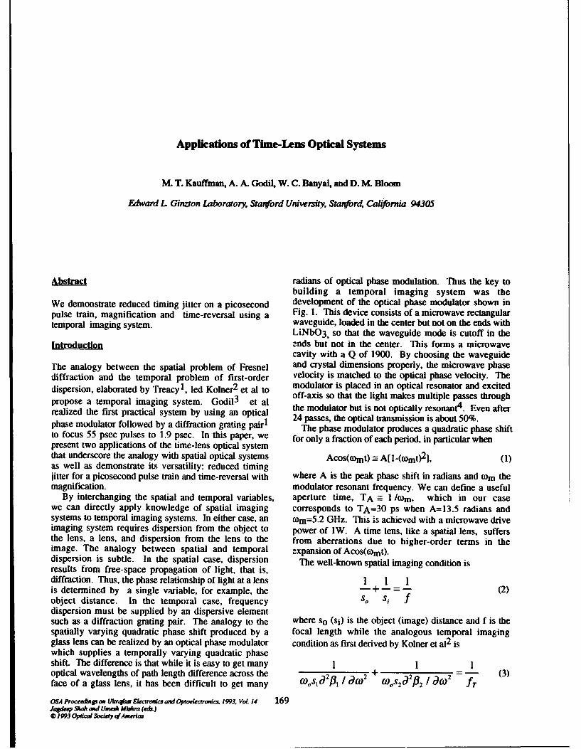
Applications of Time-Lens Optical Systems
M. T. Kauffman, A. A. Godil, W. C. Banyal, and D. M. Bloom
Edward L Ginzron Laboratory, &anford University, Stanford California 94305
Abstract radians of optical phase modulation. Thus the key tobuilding a temporal imaging system was the
We demonstrate reduced timing jitter on a picosecond development of the optical phase modulator shown inpulse train, magnification and time-reversal using a Fig. 1. This device consists of a microwave rectangulartemporal imaging system. waveguide, loaded in the center but not on the ends with
LiNbO 3 , so that the waveguide mode is cutoff in theIntroduction ands but not in the center. This forms a microwave
cavity with a Q of 1900. By choosing the waveguideThe analogy between the spatial problem of Fresnel and crystal dimensions properly, the microwave phasediffraction and the temporal problem of first-order velocity is matched to the optical phase velocity. Thedispersion, elaborated by TreacyI, led Kolner2 et al to modulator is placed in an optical resonator and excitedpropose a temporal imaging system. Godil3 et al off-axis so that the light makes multiple passes throughrealized the fmrst practical system by using an optical the modulator but is not optically resonant4 . Even afterrealiemodulathe firtoctcll system by usdciongrating opil 24 passes, the optical transmission is about 50%.phase modulator followed by a diffraction grating pair 1 The phase modulator produces a quadratic phase shiftto focus 55 psec pulses to 1.9 psec. In this paper, we for only a fraction of each period, in particular whenpresent two applications of the time-lens optical systemthat underscore the analogy with spatial optical systems Acos(comt) = A[1-(o0mt) 2 ], (1)as well as demonstrate its versatility: reduced timingjitter for a picosecond pulse train and time-reversal with where A is the peak phase shift in radians and won themagnification. modulator resonant frequency. We can define a useful
By interchanging the spatial and temporal variables, aperture time, TA = 1/O m, which in our casewe can directly apply knowledge of spatial imaging corresponds to TA=30 ps when A=13.5 radians andsystems to temporal imaging systems. In either case, an com= 5 .2 GHz. This is achieved with a microwave driveimaging system requires dispersion from the object to power of 1W. A time lens, like a spatial lens, suffersthe lens, a lens, and dispersion from the lens to the from aberrations due to higher-order terms in theimage. The analogy between spatial and temporal expansion of Acos(Omt).dispersion is subtle. In the spatial case, dispersion The well-known spatial imaging condition isresults from free-space propagation of light, that is,diffraction. Thus, the phase relationship of light at a lens 1 1 1is determined by a single variable, for example, the - +s =- (2)object distance. In the temporal case, frequency s0 si fdispersion must be supplied by an dispersive elementsuch as a diffraction grating pair. The analogy to the where so (si) is the object (image) distance and f is thespatially varying quadratic phase shift produced by a focal length while the analogous temporal imagingglass lens can be realized by an optical phase modulator condition as first derived by Kolner et a12 iswhich supplies a temporally varying quadratic phaseshift. The difference is that while it is easy to get many 1 1 1optical wavelengths of path length difference across the + -22 (3)face of a glass lens, it has been difficult to get many 0051d'fl1 / dO 2 O0 52d d d) 2
fT
OSA Procea*nw on UklIfz El ed nks and Opfoekmonocs% 1993, V13. 14 169Jaqdep 9wh and Ume Mdaiwa (ad&)* 1993 cal Scty• America
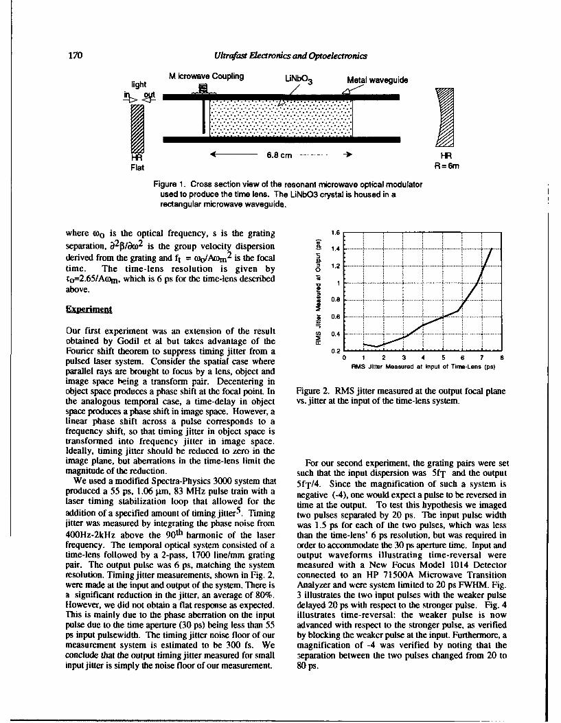
170 Ultrafast ectromnics and Optoeectronics
M icrowave Coupling UNbO3 Metal waveguide
HR 6.8 cm - HR
Flat R&
Figure 1. Cross section view of the resonant microwave optical modulatorused to produce the time lens. The LiNbO3 crystal is housed in arectangular microwave waveguide.
where oo is the optical frequency, s is the grating 1.6separation, a2p/Gb2 is the group velocity dispersion - 4
derived from the grating and ft = wo/Aoihn 2 is the focaltime. The time-lens resolution is given by oro=2.65/Ao•m, which is 6 ps for the time-lens describedabove. e
Ex~grinment S0.6
Our first experiment was an extension of the result ) 0.4 ...........obtained by Godil et al but takes advantage of the,-cFourier shift theorem to suppress timing jitter from a 0.2 ..........
pulsed laser system. Consider the spatial case where 0 1 2 3 4 5 6 7 8
parallel rays are brought to focus by a lens, object and RMS Jitter Measured at Input of Time-Lens (pa)
image space being a transform pair. Decentering inobject space produces a phase shift at the focal poinL In Figure 2. RMS jitter measured at the output focal planethe analogous temporal case, a time-delay in object vs. jitter at the input of the time-lens system.space produces a phase shift in image space. However, alinear phase shift across a pulse corresponds to afrequency shift, so that timing jitter in object space istransformed into frequency jitter in image space.Ideally, timing jitter should be reduced to zero in theimage plane, but aberrations in the time-lens limit the For our second experiment, the grating pairs were setmagnitude of the reduction. such that the input dispersion was 5fT and the output
We used a modified Spectra-Physics 3000 system that 5fT/ 4 . Since the magnification of such a system isproduced a 55 ps, 1.06 pim, 83 MHz pulse train with a negative (-4), one would expect a pulse to be reversed inlaser timing stabilization loop that allowed for the time at the output. To test this hypothesis we imagedaddition of a specified amount of timing jitter 5 . Timing two pulses separated by 20 ps. The input pulse widthjitter was measured by integrating the phase noise from was 1.5 ps for each of the two pulses, which was less400Hz-2kHz above the 9 0 th harmonic of the laser than the time-lens' 6 ps resolution, but was required infrequency. The temporal optical system consisted of a order to accommodate the 30 ps aperture time. Input andtime-lens followed by a 2-pass, 1700 line/umm grating output waveforms illustrating time-reversal werepair. The output pulse was 6 ps, matching the system measured with a New Focus Model 1014 Detectorresolution. Timing jitter measurements, shown in Fig. 2, connected to an HP 71500A Microwave Transitionwere made at the input and output of the system. There is Analyzer and were system limited to 20 ps FWHM. Fig.a significant reduction in the jitter, an average of 80%. 3 illustrates the two input pulses with the weaker pulseHowever, we did not obtain a flat response as expected. delayed 20 ps with respect to the stronger pulse. Fig. 4This is mainly due to the phase aberration on the input illustrates time-reversal: the weaker pulse is nowpulse due to the time aperture (30 ps) being less than 55 advanced with respect to the stronger pulse, as verifiedps input pulsewidth. The timing jitter noise floor of our by blocking the weaker pulse at the input. Furthermore, ameasurement system is estimated to be 300 fs. We magnification of -4 was verified by noting that theconclude that the output timing jitter measured for small separation between the two pulses changed from 20 toinput jitter is simply the noise floor of our measurement. 80 ps.
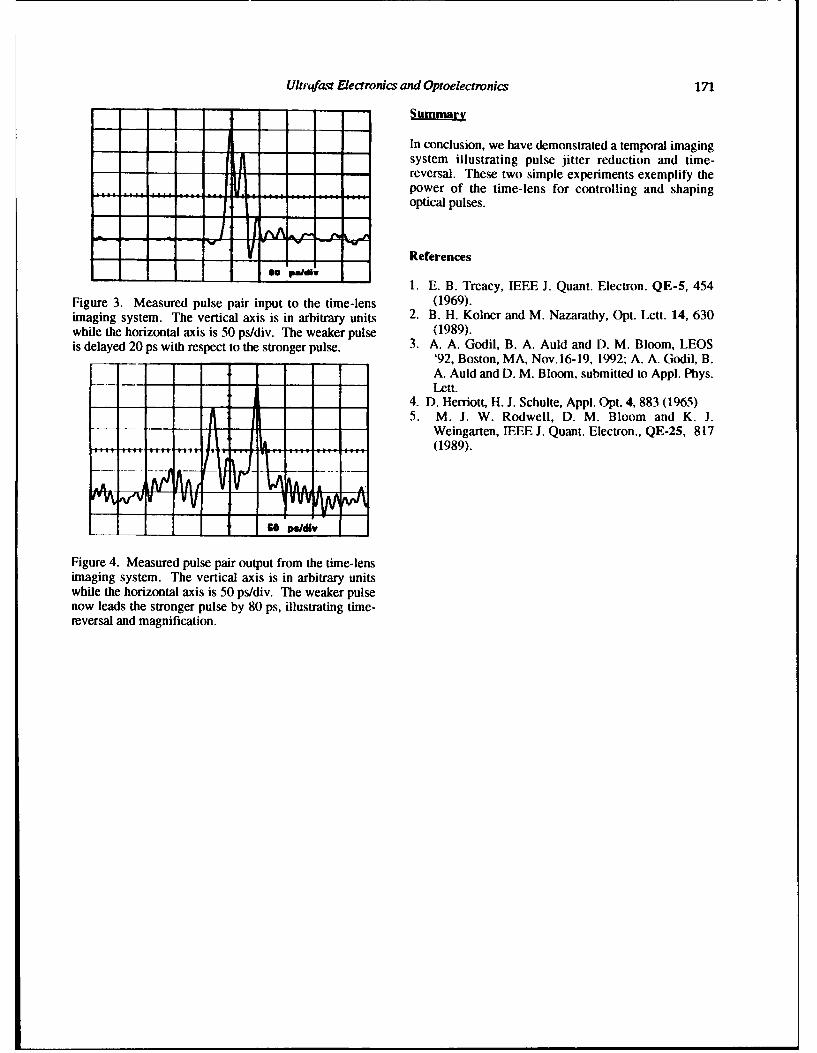
Ultrufast Electronics and Optoelectronics 171
- - Summary
In conclusion, we have demonstrated a temporal imagingsystem illustrating pulse jitter reduction and time-
-- reversal. These two simple experiments exemplify thepower of the time-lens for controlling and shapingoptical pulses.
_ - .. . . ,- ,
ReferencesamO puldllv
S-- 1. E. B. Treacy, IEEE J. Quant. Electron. QE-5, 454Figure 3. Measured pulse pair input to the time-lens (1969).imaging system. The vertical axis is in arbitrary units 2. B. H. Kolner and M. Nazarathy, Opt. Lett. 14, 630while the horizontal axis is 50 ps/div. The weaker pulse (1989).is delayed 20 ps with respect to the stronger pulse. 3. A. A. Godil, B. A. Auld and D. M. Bloom, LEOS
'92, Boston, MA, Nov.16-19, 1992; A. A. Godil, B.A. Auld and D. M. Bloom, submitted to Appl. Phys.
- -- - - -Lett.4. D. Herriott, H. J. Schulte, Appl. Opt. 4, 883 (1965)5. M. J. W. Rodwell, D. M. Bloom and K. J.
- - - -Weingarten, IEEE J. Quant. Electron., QE-25, 817---- ---- (1989).S.... .... .. ... ..... .. .... 9..
,0 poldiv
Figure 4. Measured pulse pair output from the time-lensimaging system. The vertical axis is in arbitrary unitswhile the horizontal axis is 50 ps/div. The weaker pulsenow leads the stronger pulse by 80 ps, illustrating time-reversal and magnification.
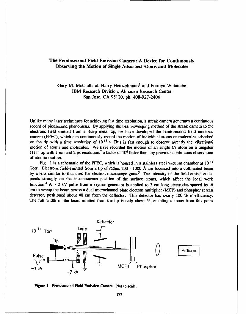
The Femtosecond Field Emission Camera: A Device for ContinuouslyObserving the Motion of Single Adsorbed Atoms and Molecules
Gary M. McClelland, Harry Heinzelmannl and Fumiya WatanabeIBM Research Division, Almaden Research Center
San Jose, CA 95120, ph. 408-927-2406
Unlike many laser techniques for achieving fast time resolution, a streak camera generates a continuousrecord of picosecond phenomena. By applying the beam-sweeping method of the streak camera to theelectrons field-emitted from a sharp metal tip, we have developed the femtosecond field emisz ioncamera (FFEC), which can continuously record the motion of individual atoms or molecules adsorbedon the tip with a time resolution of 1013 s. This is fast enough to observe ,irectly the vibrationalmotion of atoms and molecules. We have recorded the motion of an single Cs atom on a tungsten(11) tip with I nm and 2 ps resolution,2 a factor of 106 faster than any previous continuous observationof atomic motion.
Fig. I is a schematic of the FFEC, which is housed in a stainless steel vacuum chamber at 10-11Torr. Electrons field-emitted from a tip of radius 200 - 1000 A are focussed into a collimated beamby a lens similar to that used for electron microscope 6uns.3 The intensity of the field emission de-pends strongly on the instantaneous position of the surface atoms, which affect the local workfunction. 4 A - 2 kV pulse from a krytron generator is applied to 3 cm long electrodes spaced by .6cm to sweep the beam across a dual microchannel plate electron multiplier (MCP) and phosphor screendetector, positioned about 40 cm from the deflector. This detector has nearly 100 % e efficiency.The full width of the beam emitted from the tip is only about 50, enabling a focus from this point
Deflector
10-11 Torr Lens tJ
Tip
Pulse~1T 0- MCPs Phspo
-1 kY -7 --hosphor-7 kV-
Figure i. Femtosecond Field Emission Camera. Not to scale.
172
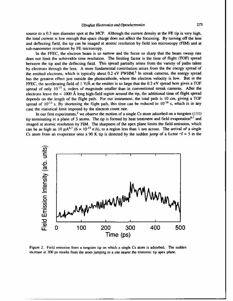
Ultrafast Electronics and Optoelectronics 173
source to a 0.3 mm diameter spot at the MCP. Although the current density at the FE tip is very high,the total current is low enough that space charge does not affect the focussing. By turning off the lensand deflecting field, the tip can be imaged at atomic resolution by field ion microscopy (FIM) and atsub-nanometer resolution by FE microscopy.
In the FFEC, the electron beam is so narrow and the focus so sharp that the beam sweep ratedoes not limit the achievable time resolution. The limiting factor is the time of flight (TOF) spreadbetween the tip and the deflecting field. This spread partially arises from the variety of paths takenby electrons through the lens. A more fundamental contribution arises from the the energy spread ofthe emitted electrons, which is typically about 0.2 eV FWHM. 5 In streak cameras, the energy spreadhas the greatest effect just outside the photocathode, where the electron velocity is low. But in theFFEC, the accelerating field of I V/A at the emitter is so large that the 0.2 eV spread here gives a TOFspread of only 1015 s, orders of magnitude smaller than in conventional streak cameras. After theelectrons leave the = 1000 A long high-field region around the tip, the additional time of flight spreaddepends on the length of the flight path. For our instrument, the total path is 10 cm, giving a TOFspread of 10-13 s. By shortening the flight path, this time can be reduced to 10-14 s, which is in anycase the statistical limit imposed by the electron count rate.
In our first experiments, 2 we observe the motion of a single Cs atom adsorbed on a tungsten (111)tip terminating in a plane of 3 atoms. The tip is formed by heat treatment and field evaporation6'7 andimaged at atomic resolution by FIM. The sharpness of the apex plane limits the field emission, whichcan be as high as 10 jgA 6 '7 (6 x 10-13 e/s), to a region less than 1 nm across. The arrival of a single
Cs atom from an evaporator onto a 90 K tip is detected by the sudden jump of a factor f1 5 in the
I-"I I
"--oL...
C/)
4.oU/)
CO
E
(Di_ 0 100 200 300 400 500Time (ps)
Figure 2. Field emission from a tungsten tip on which a single Cs atom is adsorbed. The suddenincrease at 300 ps results from the atom jumping to a site nearer the triatomic tip apex plane.
174 Ultrafast Electronics and Optoelectronics
FE caused by lowering of the local work function.8 To observe the motion of the Cs atom, the tip ispulsed negative for several ns, generating a current of several tA, which heats the Cs atom by inelasticelectron tunneling or the Nottingham effect. The resulting beam is swept and focussed to give the traceshown in Figure 2. The abrupt rise in the field emission, which occurs within the 2 ps pixel width ofour detector, indicated that a Cs atom has jumped into the < I nm dia. region on the tip observed byfield emission. The gradual rise and fall of the emission current is related to the voltage pulse shape.From the field emission image, we can determine the position of the Cs atom before and after eachsweep.
2
Even though the angle at which the electron beam leaves the tip is determined by its position onthe tip, focussing the beam on the detector screen destroys this spatial information. By using anastigmatic lens to defocus the beam perpendicular to the scan direction, simultaneous temporal andone-dimensional spatial resolution is achievable. 2 By increasing the scan rate and using higher currents,it will be possible to follow the trajectories of individual atoms and molecules on the time scale ofatomic vibration.
References1. Present address: Institute of Physics, University of Basel, 4056 Basel, Switzerland.2. Heinzelmann, H., Watanabe, F. & McClelland, G. M., submitted to Nature.3. El Gomati, M. M., Prutton, M. & Browning, R. J. Phys. E 18, 32-38 (1985).4. Woodruff, D. P. & Delchar, T. A. Modern Techniques in Surface Science (Cambridge U. Press,
Cambridge, 1986).5. Vu Thien Binh & Marien, J. Surface Sci. 202, L539-L549 (1988).6. Fink, H.-W. IBM J. Res. Develop. 30, 460-465 (1986).7. Fink, H.-W. Physica Scripta 38, 260-263 (1988).8. Todd, C. J., & Rhodin, T. N. Surface Sci. 42, 109-138 (1974).
(Sub)Millimeter Wave Devices
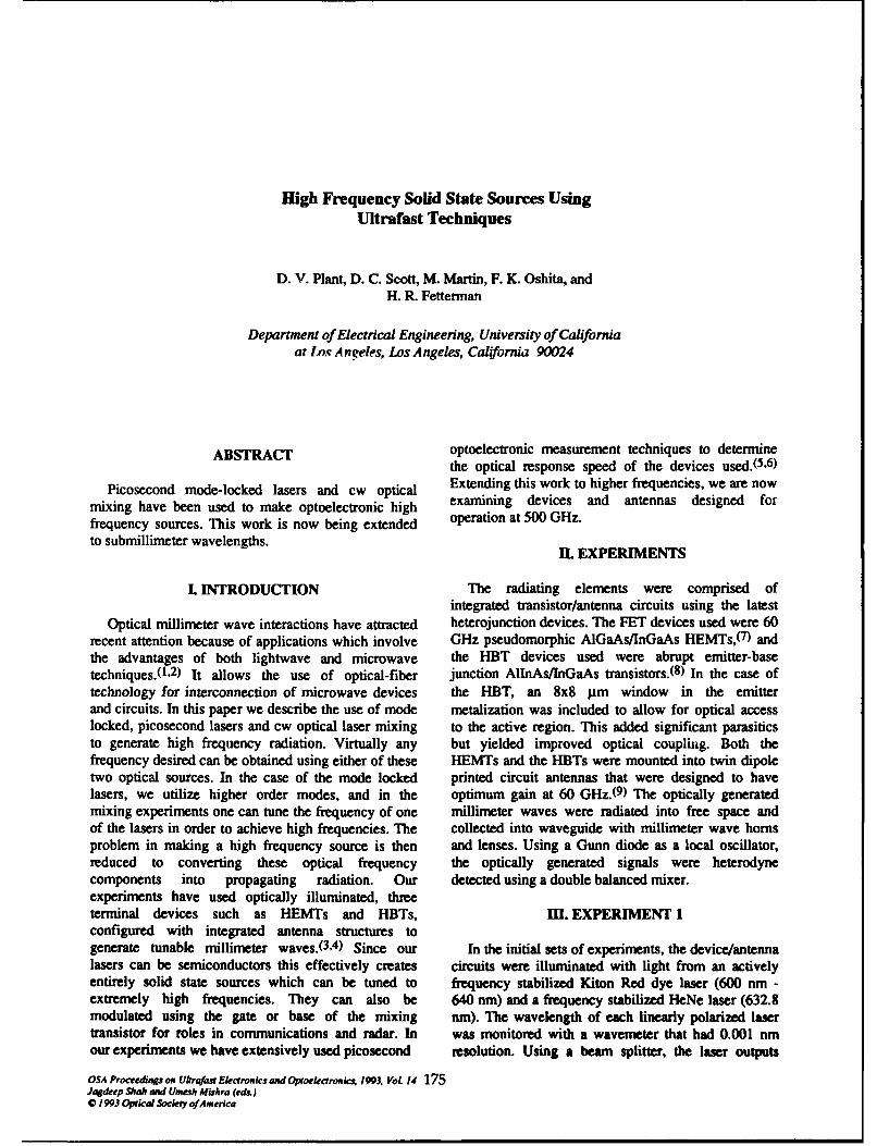
High Frequency Solid State Sources UsingUltrafast Techniques
D. V. Plant, D. C. Scott, M. Martin, F. K. Oshita, andH. R. Fetterman
Department of Electrical Engineering, University of Californiaat Los Angeles, Los Angeles, California 90024
ABSTRACT optoelectronic measurement techniques to determine
the optical response speed of the devices used.(5,6)
Picosecond mode-locked lasers and cw optical Extending this work to higher frequencies, we are now
mixing have been used to make optoelectronic high examining devices and antennas designed for
frequency sources. This work is now being extended operation at 500 GHz.
to submillimeter wavelengths. IL EXPERIMENTS
I. INTRODUCTION The radiating elements were comprised ofintegrated transistor/antenna circuits using the latest
Optical millimeter wave interactions have attracted heterojunction devices. The FET devices used were 60recent attention because of applications which involve GHz pseudomorphic AlGaAs/InGaAs HEMTs,( 7) andthe advantages of both lightwave and microwave the HBT devices used were abrupt emitter-basetechniques.( 1,2) It allows the use of optical-fiber junction AlInAs/InGaAs transistors.( 8) In the case oftechnology for interconnection of microwave devices the HBT, an 8x8 gm window in the emitterand circuits. In this paper we describe the use of mode metalization was included to allow for optical accesslocked, picosecond lasers and cw optical laser mixing to the active region. This added significant parasiticsto generate high frequency radiation. Virtually any but yielded improved optical coupling. Both thefrequency desired can be obtained using either of these HEMTs and the HBTs were mounted into twin dipoletwo optical sources. In the case of the mode locked printed circuit antennas that were designed to havelasers, we utilize higher order modes, and in the optimum gain at 60 GHz.(9) The optically generatedmixing experiments one can tune the frequency of one millimeter waves were radiated into free space andof the lasers in order to achieve high frequencies. The collected into waveguide with millimeter wave hornsproblem in making a high frequency source is then and lenses. Using a Gunn diode as a local oscillator,reduced to converting these optical frequency the optically generated signals were heterodynecomponents into propagating radiation. Our detected using a double balanced mixer.experiments have used optically illuminated, threeterminal devices such as HEMTs and HBTs, MI. EXPERIMENT Iconfigured with integrated antenna structures togenerate tunable millimeter waves.( 3 ,4 ) Since our In the initial sets of experiments, the device/antennalasers can be semiconductors this effectively creates circuits were illuminated with light from an activelyentirely solid state sources which can be tuned to frequency stabilized Kiton Red dye laser (600 nm -
extremely high frequencies. They can also be 640 nm) and a frequency stabilized HeNe laser (632.8modulated using the gate or base of the mixing nm). The wavelength of each linearly polarized lasertransistor for roles in communications and radar. In was monitored with a wavemeter that had 0.001 nmour experiments we have extensively used picosecond resolution. Using a beam splitter, the laser outputs
OSA Proceedings on Ubtrafa" Electronics and Optoelectronkc 1993, VoL 14 175Jagdeep Shah and Umesh Mishra (ed.)0 1993 Oprical Society ofAmerica
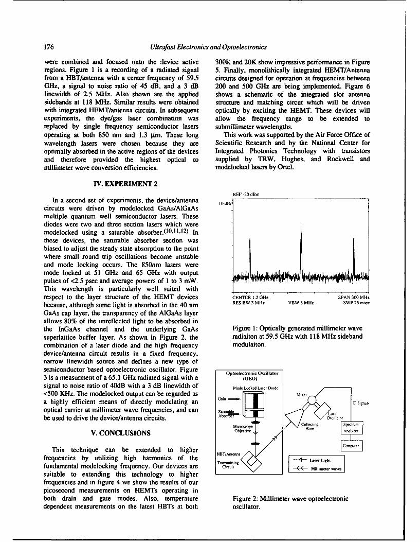
176 Ultrafast Electronics and Optoelectronics
were combined and focused onto the device active 300K and 20K show impressive performance in Figureregions. Figure 1 is a recording of a radiated signal 5. Finally, monolithically integrated HEMT/Antennafrom a HBT/antenna with a center frequency of 59.5 circuits designed for operation at frequencies betweenGHz, a signal to noise ratio of 45 dB, and a 3 dB 200 and 500 GHz are being implemented. Figure 6linewidth of 2.5 MHz. Also shown are the applied shows a schematic of the integrated slot antennasidebands at 118 MHz. Similar results were obtained structure and matching circut which will be drivenwith integrated HEMT/antenna circuits. In subsequent optically by exciting the HEMT. These devices willexperiments, the dye/gas laser combination was allow the frequency range to be extended toreplaced by single frequency semiconductor lasers submillimeter wavelengths.operating at both 850 nm and 1.3 gm. These long This work was supported by the Air Force Office ofwavelength lasers were chosen because they are Scientific Research and by the National Center foroptimally absorbed in the active regions of the devices Integrated Photonics Technology with transistorsand therefore provided the highest optical to supplied by TRW, Hughes, and Rockwell andmillimeter wave conversion efficiencies. modelocked lasers by Ortel.
IV. EXPERIMENT 2REF -20 dBm
In a second set of experiments, the device/antenna 1OdBIcircuits were driven by modelocked GaAs/AlGaAsmultiple quantum well semiconductor lasers. Thesediodes were two and three section lasers which weremodelocked using a saturable absorber.( 10. 11,12) Inthese devices, the saturable absorber section wasbiased to adjust the steady state absorption to the pointwhere small round trip oscillations become unstableand mode locking occurs. The 850nm lasers weremode locked at 51 GHz and 65 GHz with outputpulses of <2.5 psec and average powers of 1 to 3 mW.This wavelength is particularly well suited withrespect to the layer structure of the HEMT devices CENTER 1.2 GHz SPAN 300 MHz
because, although some light is absorbed in the 40 nm RES BW 3 MHz VBW 3 MHz SWP 25mec
GaAs cap layer, the transparency of the AIGaAs layerallows 80% of the unreflected light to be absorbed inthe InGaAs channel and the underlying GaAs Figure 1: Optically generated millimeter wavesuperlattice buffer layer. As shown in Figure 2, the radiaiton at 59.5 GHz with 118 MHz sidebandcombination of a laser diode and the high frequency modulaiton.device/antenna circuit results in a fixed frequency,narrow linewidth source and defines a new type ofsemiconductor based optoelectronic oscillator. Figure Optoelectronic Oscillator
3 is a measurment of a 65.1 GHz radiated signal with a (OEO)signal to noise ratio of 40dB with a 3 dB linewidth of Mode Locked Laser Diode
<500 KHz. The modelocked output can be regarded as Gi iea highly efficient means of directly modulating an ISgaoptical carrier at millimeter wave frequencies, and can Saturable Local
be used to drive the device/antenna circuits. Absorbe ,"I'/amr C l e t ng O , p el a tr u
41• Ni/q~CO'I entgS.na ,Microscope Hor
V. CONCLUSIONS objectiýrv e ,z
This technique can be extended to higher HBT/Ante
frequencies by utilizing high harmonics of the Trantting LasrLight
fundamental modelocking frequency. Our devices are Circuit *<Millimeterwvsuitable to extending this technology to higherfrequencies and in figure 4 we show the results of ourpicosecond measurements on HEMTs operating inboth drain and gate modes. Also, temperature Figure 2: Millimeter wave optoelectronicdependent measurements on the latest HBTs at both oscillator.
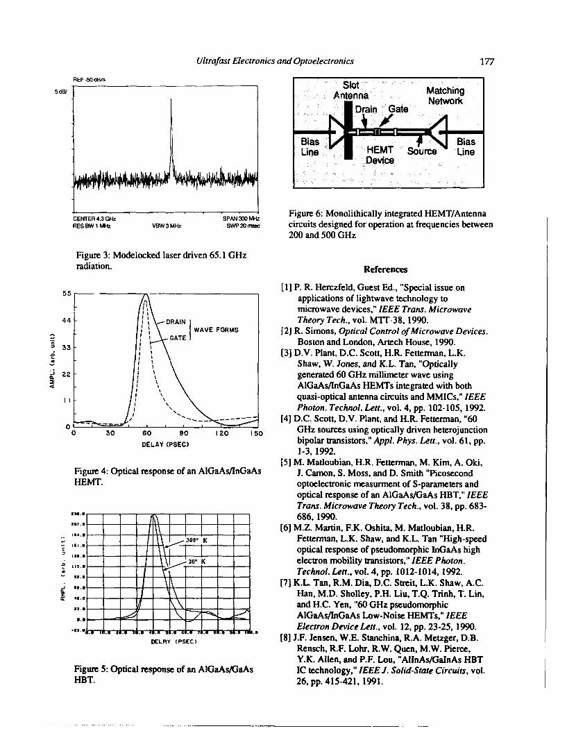
Ultrafast Electronics and Optoelectronics 177
5dIREF -50 dflmsltMchn
LineHEMT source LineDevice
CENTR 4. G~ SPA 300M~z Figure 6: Monolithically integrated HEMT/AntennaRES OW 1 Mtz VOW 3 Mt4Z SWP 20 ffmc circuits designed for operation at frequencies between
200 and 500 GHz
Figure 3: Modelocked laser driven 65.1 GHzradiation. References
55 [11] P. R. Herczfeld, Guest Ed., "Special issue onapplications of lightwave technology tomicrowave devices," IEEE Trans. Microwave
44 - DORAI Theory Tech., vol. M17-38, 1990.GAEWAVE FORMS [2] R. Simons, Optical Control of Microwave Devices.
= I 'Boston and London, Artech House, 1990.A [31 D.V. Plant, D.C. Scott, H.R. Fetterman, L.K.
Shaw, W. Jones, and K.L. Tan, "Optically0j ? generated 60 GHz millimeter wave using
I AIGaAs/InGaAs HEMTs integrated with both
quasi-optical antenna circuits and MMICs," IEEEPhoton. Technol. Lett., Vol. 4, pp. 102-105, 1992.
/ ------ [4] D.C. Scott, D.V. Plant, and H.R. Fetterman, "6001
0 30 so 90 I 20 150 GHz sources using optically driven heterojunctionDELAY (PSEC) bipolar transistors," App!. Phys. Lett., Vol. 61, pp.
1-3, 1992.[5] M. Matloubian, H.R. Fetterman, M. Kim, A. Old.
Figure 4: Optical response of an AIGaAs/InGaAs J. Cainon, S. Moss, and D. Smith "PicosecondHEMT. optoelectronic measurment of S-parameters and
optical response of an AlGaAs/GaAs HBT," IEEETrans. Microwave Theory Tech., Vol. 38, pp. 683-
- -T - -686,1990.
- - - -[61 M.Z. Martin, F.K. Oshita, M. Matloubian, H.R.1 -. 300 -K Fettermian, L.K. Shaw, and K.L. Tan "High-speed
cc S1 optical response of pseudomorphic lnGaAs high
2*K electron mobility transistors," IEEE Photon.*21 - - - - -Technol. Lett., vol. 4, pp. 10 12-1014, 1992.
[17 K.L. Tan, R.M. Dia, D.C. Streit, L.K. Shaw, A.C.46.1 Han, M.D. Sholley, P.H. Liu, T.Q. Trinh, T. Lin,
- - -- - - -and H.C. Yen, "60 GHz pseudomorphic:AlGaAsIInGaAs Low-Noise HEMTs," IEEE
~ ~ -, ..- ~. ,. .u- .. Electron Device Lett., vol. 12, pp. 23-25, 1990.DELAY PSEC)[81 J.F. Jensen, W.E. Stanchina, R.A. Metzger, D.B.
Rensch, R.F. Lohr, R.W. Quen, M.W. Pierce,Y.K Allen, and P.F. Lou, "AlInAs/GaInAs HBT
Figure 5: Optical response of an AIGaAs/GaAs IC technology," IEEE J. Solid-State Circuits, vol.HBT. 26, pp. 415-421, 1991.
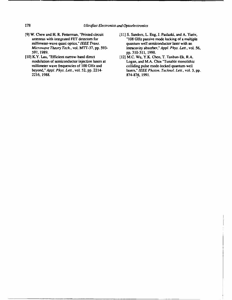
178 Ultrafast Electronics and Optoelectronics
[91 W. Chew and H. R. Fetterman, "Printed circuit [11] S. Sanders, L. Eng, J. Paslaski, and A. Yariv,antennas with integrated FET detectors for "108 GHz passive mode locking of a multiplemillimeter-wave quasi optics," IEEE Trans. quantum well semiconductor laser with anMicrowave Theory Tech., vol. MTT-37, pp. 593- intracavity absorber," Appl. Phys. Lett., vol. 56,597, 1989. pp. 310-311, 1990.
[101 K.Y. Lau, "Efficient narrow-band direct [12] M.C. Wu, Y.K. Chen, T. Tanbun-Ek, R.A.modulation of semiconductor injection lasers at Logan, and M.A. Chin "Tunable monolithicmillimeter wave frequencies of 100 GHz and colliding pulse mode-locked quantum-wellbeyond," Appl. Phys. Lett., vol. 52, pp. 2214- lasers," IEEE Photon. Technol. Lett., vol. 3, pp.2216, 1988. 874-876, 1991.
On-Wafer Optoelectronic Techniques forMfillimeter-Wave Generation, Control, and
Circuit Characterization
Sheng-Lung L. Huang and ChM H. LeeElectrical Engineering Department, University of Marylanit
College Park, Maryland 20742
Hing-Loi A. HungCOMSA TLaboratories, Clarksburg, Maryland 20871
Abstract Experimnents
Using 0 1 )t( )lect r( )ic techniqui1 es, the generation alnd The NIMXX genera tion) and( true- tinle-delay phlase-
t rue-t ilne-(lelav 1 )hase-sllift of G0-Gliz b)roadb1and shift are aclievedl using a. 5-ps electrical pl-lls(, while
signals. as well ais on-wafer circuit. cha~ract~erizat~ion the circuit characterization is obtained wvith both
exceed1ing 160 0Hz, which is (-lose the bandwidth 5-ps and 2 .S-ps electrical pulses. For both experi-
limit of inhirostrip transmnissioni line onl a. 4-muli thick ninents, the electrical pulses are geniera~ted by the pho-
GaAs wafer, have b~eeni dlemnlstratedl. toconductive (PC) effect.. The laser systemi gener-
ates both 3 -ps and 400-fis green pulses from a. mlode-
Introduction locked Nd:YLF laser which 1)111111) a first stage fiber-
grating pu1lse~ compressor followed by a frequency
Recent pr-ogresses inl the merging of ultrafast. op- doubling crystal (3 lps) andl a secondl stage fiber-
tics and1( high speed( electronic circuit techniques 1)11511 pu1lse comp1Iressor (400 fs). The average power
have resizlted inI a wniuber of new p~otenltial appli- requiredl is less than 10 niWX. The electrica~l pulses
cations. 0mm-wafer oIptoclectrolilc technmiques refer contain frequency components well beyond 200 GHz.
to the class of techniques where oIptic/electrnOflin-~ The pho~t~ocondullctive switch is 10 pin long and wvas
tcrinixing structures canl be integrated with elec- fabricated onl a 4-inil-thmick GaAs wafer. The GaAs-
tronic circuits to achieve various circumit character- material gal) ini PC switch was proton impllanlted
ization and component. functions. InI this pl.Pe1¾ at. a (lose of 1014 cnm2-. The fabrication pro~cess is
a niew imnetla x of genmerat ing b othl inillimneter-wa~ves fully com)npa tible with cuirrent inicr( wave/mmmillimneter-
(NIMWs) and true-timec-delay phlase-shift~s of GO wave integra~tedl circuit (MIMIC) technologies; there-
0Hz broadband signals, is presented. This optical fore, all the op~tical structures used to achieve the
technique is usefuil in applications such as, broad- functions we, demlonlstrate can b)e integralted with
band phased ariray anitennas and communication sys NMICs. Figure 1 shows the schematic of the MMIC
teilns [1]. We have also extended time ol)tical charac- and optical test strutctuire.
terization of monolithic integrated circuits beyond
160 0Hz [21 [3].
GSA Proceedfings on Ubrafanr Elearonics and Oproeveirnics, 1993, Vol. 14 179Jagdeep Shah and UnkMesi, Aah teds.)o 1993 Optical Society ofAmnurca
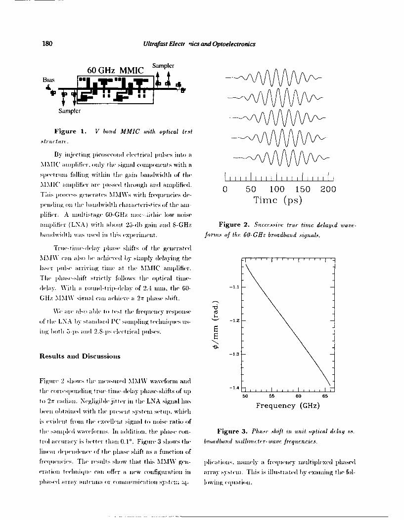
180 Ultrafost Electr 'tics and Optoelectronics
60 GHz MMIC Sampler
Biasga qrM' q
Sampler
Figure 1. V band MMIC w~ith optical test
.4trut arf I II T
Byv itiljet ing p)icos)econd~ electrical plsesin(5jto) a
\1I(atii 1 )liiher, onily thec Signial c()ilpivi)l~lts with a
sjpecti-I till falling Wit hini the gainl laii(Iwidltl of the IIII
MMI(ilpifiq iie ate, passed t hroutghi aili amjiphfiedl. 0 50 1 00 1 50 200Thisl, priicss generiates NUINIX-s with fre(1tteicies de- Timne (p s)pen~idinig onl t li li('aldwilth ii cli racteristics of the aml-
;)lifier. A nitiltistage G0-GHz ilio:iitdihic low iloisv
attijlihecr ( LNA ) with albowl 23-dh gain and S-GHz Figure 2. Saccesqsive trite time delayecd ivave-
bandwidth Was tiseil ill tll-, experinlient. form,,, of thc 60- GHz broadband signals.m
Trite- timie-elelay phase shifts of the geiierateil
M.MX can also 6f, achicved by sli~iiplv dlelayinig the
laser. plitie arriving tinhic at the MIMIC apiir
The 1 ihase-shift strictly follows the optical timie-
delay. W~ith a ni~iinl-t ri)-(lelav of 2.4 1111, the 60-
GHz N1IX iviial cani achieve a 2-, jiliase shift.
of thle L. A by st andidmu PC' samlniitg teclitii(jltes lis- -1.2
itig bo1 th 5i-1, andi i 2.S-p 1)5 (htrical pullses.
Results and~ Discussionis -1.3
Figure- 2 shows the( iiieasiiredA MMXV waveformn andh5 5 0 6tlie corrlespidiniig r-ite- tittie- delay 1)liase-sliifts of up) 1,
to 27- radian. .Negligiblde jitter- inl thle LNA signal hasFrqec Gzbeenl olbtainted with the liresetit systeml setuip. whichFeqe y(G-z
is evidenit from ith le excelletnt signtal to tioise ratio oif
the samptlledl wavef irnis. Ill addition. the lplias(' coil- Figure 3. Phase'c shaft In uni.t optical dlay n5.s
ttol accuriacy is better than 0.1'. Figure 3 shows the broadband. mndlljmrctr- ira-t frequencies.
linear &-pendleitce of the piihase shift, as a fittictionl of
freqicteicies. The results sho1w that this MMXVI geit- plica It io ins. nianiely a freeptei(ic(y titutltiplexed phits-ed
era t ut teelitiqutec call offet a new configuriation inl array syst ciii. This is Illustrated by exanung thli fol-
lplase~l array aittteitta (i or itt~iCiit ytu ap lowing equlation.
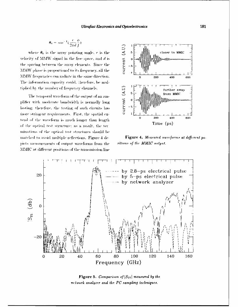
Ultrafast Electronics and Optoelectronics 181
Wilieie 0o is the rivpoinltinig angle. c is the -11 .5 closer to MMIC
ve ot(f NBINV sipgial inl the freco Space, anld (I is * 0
the' sp)aci1g Iit e* thli array ('1('illelt~s. Since-4 the -.
INMM" phlase is, pr p)Iortla iiia to Its frqitc.all the :5coetoM
\1\lMt foqueIicicic- scall radilite Ill t he sallie dlirectionii. 0 200 400 600
The Informtiona capacaity could1. lierefore, Ibe mnid-
tiplied(I 1 y t lieii it 1(1be of fre(1 iviel y chliajitels. 1 l****D~ h further awayF) hIIII from MMIC
Thci telilil ial wax-cf uni of the output oif anl am-
Ifliher With Ii oderate lmn lwilt h is normally long l 11!Ilasting: t heref ire, the te'stinlg of Such Circuits has.'
tIn ire stinlg('It reqjulileiielt s. First. thet spatial ex- IL
teld oIf thle 'wavefclIrii is muc1h.1 lonlger thanl length T0m (ps)00 60
(If tilie optical test si mict ire: as a residt . the tWi Tm (s
111111ations. if t ilt, op~tical test striuctires Shiouild I1v
mnat ehed to avol nitidltiple reflections. Figure 4 de- Figure 4. Mcaurci -ivud v cfoarw.q at dzfforrrnt po-
1 )jcts nicatisurciiiiits (if ouitpuiit waxvefornis fronm the -tht of thV MMIC oiutputt.
MMIC at diflemenit positions of thlt transmission line
-- - - - - - - - - ------by 2.8-ps electrical pulse20 f ' - - by 5-ps electrical pulse
I \by network analyzer
CO ItIt
-20 1 .p Yl to 1
0 20 40 60 80 100 120 140 160
Frequency (GHz)
Figure 5. C077JPari.qO1 Of IS2 1 1 mcaqurtrd by thr~nctwt~ork analyzer and thr PC -tampling techniques.q
182 Ulttwfast Electronics and Optoelectronics
Two) 114 j41 4mdi,.t piptl1n.! wmv4" withI (1it14'14'lt 114114' illiim, shift ()f 601 G H/ hi-oiidl ,uid signals. Tli c(41114
'11111o 11) 4'ifcicit t4'l4j441it wavt'foiiii1s. Sec- 4'11114114 111(v '( p im~ IIl14\ systt'Iiis I)N ;Ill(wing fn'qupelicy
(41141. "11144- Owt m.;ipilin't. tullei'. ",ug. the boImI. tcrutl uoIti61,dexiiig. WC ;11544 mv;easured lii' f-cilcqiiIovit-
stillýi1jt.\ 441* III4' 11111ia1144t Is~4' IS 1-114j14 foIn r4'laet '~J4ImI>4 ()f a MINIC amplIiticI over(, 160 ;Hz band1(-
1111,dilleleirt p1II54 w1idth,' ;it( sho(wn1 III Figul-c4 3. limiit fon ml4'1,'-tupline 1u114 d N05( IMI(. The faulniea
vIdth 1, isap)p1'icloltCIV inc4'4'aw'1 to o)ver 160 CII,. _NINI( 44'I1tI4
( If/ 41lnldVwj4thI. ]flns 111l'lsl4111('11Clt ,-l10\s that thel d(vIs?1 Il Pm14t Iw.11e11i 1( jI g1;1111.
-'''(41 111( lljonc l)(mvl' diistoitionl fuoiu thet LN.A is
14- thanii 10-1 -(If t1he f11114amc1a'1a G0-IH/, signal. References
0111 0411 ~vittPC sltll1pIing t4'11i1 1 114'qu can1 beI 1(ijllstecl I* .\.1. aillmilx. '-P11115(4 Aiiay 7fhaoxwy and1
,() Iliit It 1, w4';4l enoug1.I.h toa(4 I d14itl (ljt(4110. whlile. Tv('ImoI(lgy.- Proc. IEEE, 70. pp. 246 291.st~ilt 14 11(4-11 4itl 144 ivt high dlllailllic raligI'. 9.
2. lILL. A. llmiig. 1'. Polak-Dingeks K. .J. \\ehh.
T.- Smuith. H. (C. Hiuag. and C. H. Lev.C o ac i us oll Ž%1i1111(c't 4'-av Nb)1I(M4 1t4lit hi' 114 gi'a~ted Cir1cuit
('h;4aeaterizat~iol byV a Pw(')5loiilh ()pto4lec-
Omi 144114 4 elIiljle." IEEE Microwave Theory
ThlE Hi14'4imia(m14 41 (If 41)pto)4'l4'4' 1)114' t('4I~lliquesInto T114v141.. M WT -37. pp. 1223 1231. 1989.
NIMN\V svs1 ('111;1 ha lv14at 4'd a necw class o)f c11rcuits 3. S. L. Mianug. L. P. G h lb. C. H. Lve' aind H- L.
that can(1 p('rfonlo1 clectnmluic funlctions hot easily at- A. Huing. ''A no1vel ap)11-)ac11 14) 1Imma1ture pilo-
tdilldIa14' by pV1)11iteI''I)~ 111CMIS1. Synclu-imiizati'nu t4'(w(11i114tive' "'.ajImping of llI4'1)Waveil lIrCullt5.
hewei thIc4''4i 1114 it rf;fat 4IjIIiClcaI pitisI I ;iiln. and4 NI NIXV D g. (C'yvJ Lamrr.,, and Eluc tro-O(pt., pipei-
nwk4's it ('14514 144 ('4)11110 MNII'V de4vices' aild( ('irt-cui1. .JFD2. AnI;14i111i. CA.~. May 1992.
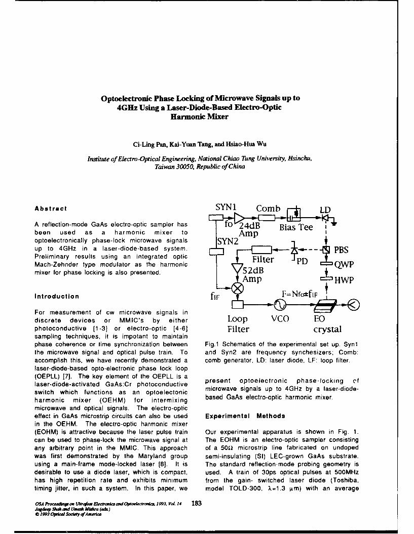
Optoelectronic Phase Locking of Microwave Signals up to4GHz Using a Laser-Diode-Based Electro-Optic
Harmonic Mixer
Ci-Ling Pan, Kai-Yuan Tang, and Hsiao-Hua Wu
Institute of Electro-Optical Engineering, National Chiao Tung University, Hsinchu,Taiwan 30050, Republic of China
AbstractFSC
A reflection-mode GaAs electro-optic sampler has fO 24dB Bias Teebeen used as a harmonic mixer to Ampoptoelectronically phase-lock microwave signals SYN2up to 4GHz in a laser-diode-based system. PBSPreliminary results using an integrated opticMach-Zehnder type modulator as the harmonic PD if= OWPmixer for phase locking is also presented. 52dBL AtHf pmp 1 W
Introduction f "r F= N fcatfi F
For measurement of cw microwave signals indiscrete devices or MMIC's by either Loop VCO FOphotoconductive [1 -3] or electro-optic [4-6] Filter crystalsampling techniques, it is impotant to maintainphase coherence or time synchronization between Fig.1 Schematics of the experimental set up. Synithe microwave signal and optical pulse train. To and Syn2 are frequency synchesizers; Comb:accomplish this, we have recently demonstrated a comb generator, LD: laser diode, LF: loop filter.laser-diode-based opto-electronic phase lock loop(OEPLL) [7]. The key element of the OEPLL is alaser-diode-activated GaAs:Cr photoconductive present optoelectronic phase-locking cflaswitch wi fun-ctionsed as ahoptoectondtie microwave signals up to 4GHz by a laser-diode-sw itch w hich functions as an optoelectonic b s d G ~ l c r - p i a m n c m x rharmonic mixer (OEHM) for intermixing based GaAs electro-optic harmonic mixer.microwave and optical signals. The electro-opticeffect in GaAs microstrip circuits can also be used Experimental Methodsin the OEHM. The electro-optic harmonic mixer(EOHM) is attractive because the laser pulse train Our experimental apparatus is shown in Fig. 1.can be used to phase-lock the microwave signal at The EOHM is an electro-optic sampler consistingany arbitrary point in the MMIC. This approach of a 500 microstrip line fabricated on undopedwas first demonstrated by the Maryland group semi-insulating (SI) LEC-grown GaAs substrate.using a main-frame mode-locked laser [8]. It is The standard reflection-mode probing geometry isdesirable to use a diode laser, which is compact, used. A train of 30ps optical pulses at 500MHzhas high repetition rate and exhibits minimum from the gain- switched laser diode (Toshiba,timing jitter, in such a system. In this paper, we model TOLD-300, ).=1.3 lam) with an average
OSA Ph-oceedingron UWtrtcv Elemm and Optoeecroum, 1993, Vol. 14 183Jaqdq, Su* and Umte, MNidra (edt)* 193 opdna Socdey ,fAm•,,a,
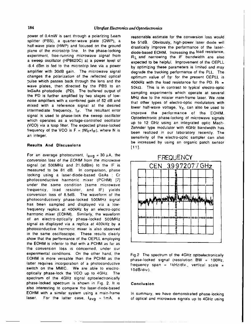
184 Ultrafast Electronics and Optoelectronics
power of 0.4mW is sent through a polarizing team reasonable estimate for the conversion loss wouldsplitter (PBS), a quarter-wave plate (QWP), a be 51dB. Obviously, high-power laser diode willhalf-wave plate (HWP) and focused on the ground drastically improve the performance of the laser-plane of the microstrip line. In the phase-locking diode-based EOHM. Increasing the load resistance,experiment, free-running microwave signal from RL and narrowing the IF bandwidth are alsoa sweep oscillator (HP8620C) at a power level of expected to be helpful. Improvement of the OEPLL-8.4 dBm is fed to the microstrip line via a power by optimizing these parameters is limited and mayamplifier with 30dB gain. The microwave signal degrade the tracking performance of the PLL. Thechanges the polarization of the reflected optical optimum value of fIF for the present OEPLL ispulse which passes back through the lens and the 400kHz with the load resistance for the PD. Ri =
wave plates, then directed by the PBS to an 50kQ. This is in contrast to typical electro-opticInGaAs photodiode (PD). The buffered output of sampling experiments which operate at severalthe PD is further amplified by two stages of low- MHz due to the noisier main-frame laser. We notenoise amplifiers with a combined gain of 52 dB and that other types of electro-optic modulators withmixed with a reference signal at the desired lower half-wave voltage, Vn, can also be used tointermediate frequency, fiF. The resultant error improve the performance of the EOHM.signal is used to phase-lock the sweep oscillator Optoelectronic phase-locking of microwave signalswhich operates as a voltage-controlled oscillator(VC) va aloo fiter Th exectd paseloced up to 12 GHz using an integrated optic Mach-(VCO) via a loop filter. The expected phase-locked Zehnder type modulator with 4GHz bandwidth hasfrequency of the VCO is F = (Nfo+flF), where N is been realized in our laboratory recently. Thean integer. sensitivity of the electro-optic sampler can also
be increased by using an organic patch sensorResults And Discussions [11]
For an average photocurrent, lavg = 30 gA, the FREQUENCYconversion loss of the EOHM from the microwavesignal (at 500MHz and 21.6dBm) to the IF is CEN 3.997207'/GHzmeasured to be 81 dB. In comparison, phaselocking using a laser-diode-based GaAs : Crphotoconductive harmonic mixer (PCHM) [7]under the same condition (same microwavefrequency, load resistor, and IF) yieldsconversion loss of 8.5dB. The waveform of thephotoconductively phase-locked 500MHz signal ,TJhas been sampled and displayed via a low-frequency replica at 400kHz by an electro-opticharmonic mixer (EOHM). Similarly, the waveformof an electro-optically phase-locked 500MHz . . .. .. .... .......... .signal as displayed via a replica at 400kHz by aphotoconductive harmonic mixer is also observedin the same oscilloscope. These results clearlyshow that the performance of the OEPLL employingthe EOHM is inferior to that with a PCHM as far asthe conversion loss is concerned, under ourexperimental conditions. On the other hand, the Fig.2 The spectrum of the 4GHz optoelectronicallyEOHM is more versatile than the PCHM as the phase-locked signal (resolution BW = 100Hz,latter requires incorporation of a photoconductive frequency span = l kHz/div., vertical scale =
switch on the MMIC. We are able to electro- 1OdB/div).optically phase-lock the VCO up to 4GHz. Thespectrum of the 4GHz signal optoelectronicallyphase-locked spectrum is shown in Fig. 2. It is Conclusionalso interesting to compare the laser-diode-basedEOHM with a similar system using a main-frame In summary, we have demonstrated phase-lockinglaser. For the latter case, lavg = lmA, a of optical and microwave signals up to 4GHz using
Ultrafast Electronics and Oproelectronics 185
a compact laser-diode-based GaAs electro-optic microwave propagation and distortionsampier as an optoelectronic harmonic mixer in characteristics of traveling-wave amplifiersthe PLL. Comparisons of the present approach studied by electrooptic sampling," IEEE Trans.with systems employing main-frame lasers or a Microwave theory Tech., 34, 1356-1362photoconductive switch as the harmonic mixer are (1 986).also presented. The upper bound for the frequency 5. K. J. Weingarten, M. J. W. Rodwell, andof the phase-locked signal in the present work is D.M.Bloom, "Picosecond optical sampling oflimited by the available average power and pulse GaAs integrated circuits," IEEE J. Quantumwidth of the laser diode, as well as Vn of the Electron., 2A, 198-220 (1988).
GaAs material . We have also suggsted methods 6. J. M. Weingarten and M. S. Heutmaker,for alleviating these problems such that our "Frequency response of an internalamplifier inscheme can be used for phase locking of optical a high-speed integratedcircuit measured byand millimeter wave signals at the wafer level. electrooptic sampling," Electron Lett., 24,
106-107 (1988).
Acknowledgments 7. H. H. Wu, C. S. Chang, and C. L. Pan,"Optoelectronic phase-locking of microwave
The authors would like to thank Prof. C.-S. Chang signals up to 18Ghz by a laser-diode-basedfor helpful discussions. This work was supported GaAs:Cr photoconductive harmonic mixer,"in part by the National Science Council of the IEEE Microwave Guided Wave Lett., 2, 11-13Republic of China under grants, NSC80-0417-E- (1992).009-05, NSC81-0417-E-009-629 and 630. 8. M.G.Li, - A.Chauchard, C.H.Lee, and H.-L.
A.Hung, "Intermixing optical and microwave
References signals in GaAs microstrip circuits for phase-locking applications," 1EEE Trans. Microwave
1. H.- L. A.Hung, P. Polak-Dingels, K. J. Webb, T. Theory Tech., 38, 1924-1931 (1990).Smith, H. C. Huang, and C. H. Lee, 9. M.G.Li, S.-L.L.Hung, C.H.Lee, and H.-L. A."Millimeter-wave monolithic integrated circuit Hung, "Display of Microwave Waveform via acharacterization by a picosecond optoelectronic low freauencv reolica usino an ootical ohase-technique," IEEE Trans Microwave Theory locking and sampling technique," in PicosecondTech., 37, 1223-1230 (1989). Electronics and optoelectronics, 1991,
2. M.Matloubian, S.E.Rosenbaum, H.R Fetterman, Technical Digest Series, (opticl society ofand P.T.Greiling, "Wideband millim:e-r-wave America, Washington, DC 1988), pp.24-27.characterization of sub-0.2 micrometer gate 10. H. H.Wu, C.S.Chang, and C. L. Pan, "A laser-length AlIn/GalnAs HEMT's," IEEE Microwave diode-based photoconducyive harmonic mixerGuided WAve Lett., 1, 32-34 (1991). for microwave waveform and spectrum
3. D. H. Auston, "Picosecond photoconductivity: measurements," IEEE Microawave GuidedHigh-speed measurements of devices and Wave Lett., 2, 273-275 (1992).materials,"in measurement of High Speed 11. T. Nagatsuma, m. Yaita, M. Shinagawa, M.Signals in Solid State Devices,Semiconuctors Amano, and Y. Shuto, "Organic patch sensorand Semimetals, vol.28, R.B.Marcus, Ed. New for elecyro-optic measurement of electricalyork: Academic Press, 1990, pp. 85-134. signals in integrated circuits, "Electron. Lett.,
4. M.J.W.Rodwell, M. Riaziat, K. J. Weingarten, 2Z, 932-934 (1991).B. A. Auld, and D. M. Bloom, "Internal
Photoconductive and Electro-Optic Sampling
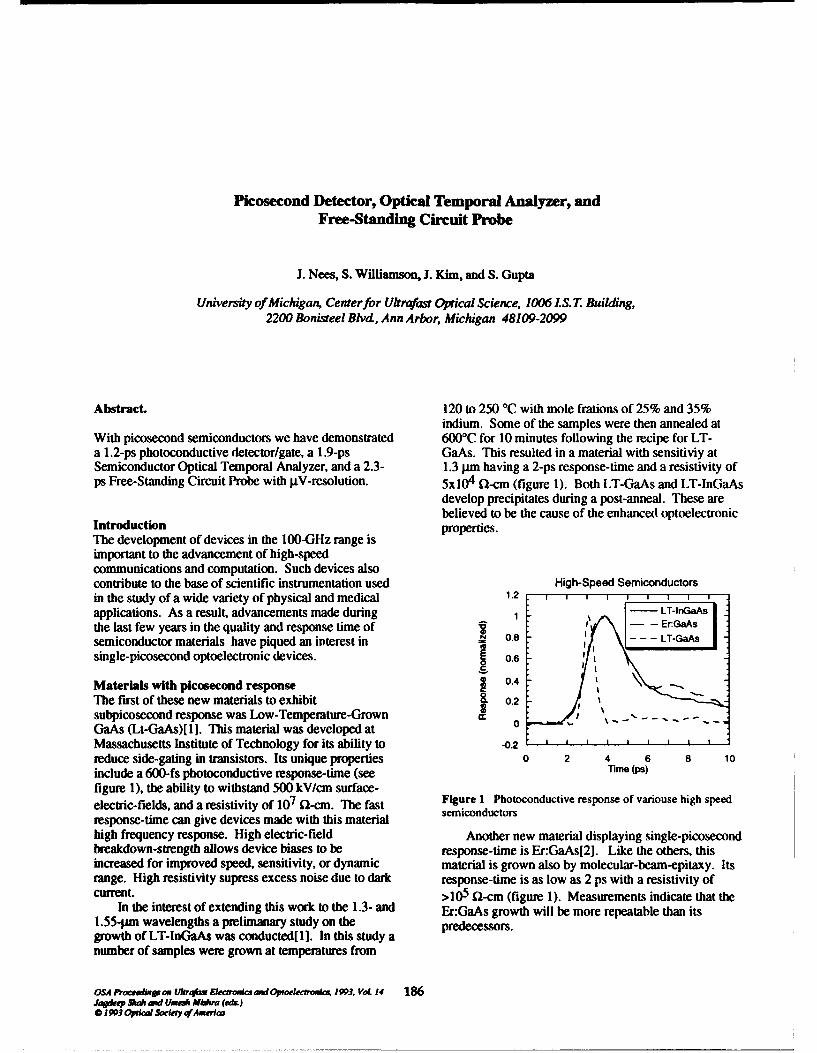
Picosecond Detector, Optical Temporal Analyzer, andFree-Standing Circuit Probe
J. Nees, S. Williamson, J. Kim, and S. Gupta
University of Michigan, Center for Ultrafast Optical Science, 1006 LS. T. Building,2200 Bonisteel Blvd, Ann Arbor, Michigan 48109-2099
Abstract. 120 to 250 °C with mole frations of 25% and 35%indium. Some of the samples were then annealed at
With picosecond semiconductors we have demonstrated 600*C for 10 minutes following the recipe for LT-a 1.2-ps photoconductive detector/gate, a 1.9-ps GaAs. This resulted in a material with sensitiviy atSemiconductor Optical Temporal Analyzer, and a 2.3- 1.3 p~m having a 2-ps response-time and a resistivity ofps Free-Standing Circuit Probe with jtV-resolution. 5x10 4 (i-cm (figure 1). Both LT-GaAs and LT-InGaAs
develop precipitates during a post-anneal. These arebelieved to be the cause of the enhanced optoelectronic
Introduction properes.The development of devices in the 100-GHz range isimportant to the advancement of high-speedcommunications and computation. Such devices alsocontribute to the base of scientific instrumentation used High-Speed Semiconductorsin the study of a wide variety of physical and medical 1.2 1 1 1 ,applications. As a result, advancements made during I LI-ErGaAs
the last few years in the quality and response time of E~~semiconductor materials have piqued an interest in . 0.8 -single-picosecond optoelectronic devices. 0.6
Materials with picosecond response 0.4
The first of these new materials to exhibit 0.2subpicosecond response was Low-Temperature-Grown c . .. .. .GaAs (Lt-GaAs)[1]. This material was developed at
Massachusetts Institute of Technology for its ability to -02reduce side-gating in transistors. Its unique properties 0 2 4 6 8 10include a 600-fs photoconductive response-time (see 'ine (Ps)figure 1), the ability to withstand 500 kV/cm surface-electric-fields, and a resistivity of 107 0-cm. The fast Figure c Photoconductive response of variouse high speedresponse-time can give devices made with this materialhigh frequency response. High electric-field Another new material displaying single-picosecondbreakdown-strength allows device biases to be response-time is Er:GaAs[2]. Like the others, thisincreased for improved speed, sensitivity, or dynamic material is grown also by molecular-beam-epitaxy. Itsrange. High resistivity supress excess noise due to dark response-time is as low as 2 ps with a resistivity ofcurrent. >105 f(-cm (figure 1). Measurements indicate that the
In the interest of extending this work to the 1.3- and Er:GaAs growth will be more repeatable than its1.55-jmn wavelengths a prelimanary study on the predecessors.growth of LT-InGaAs was conducted[l 1]. In this study anumber of samples were grown at temperatures from
OSA Prm#Aah an ,11wqfam Mea onks ad Oproeiecfim 1993, VoL 14 186iagdeep Nkh amd Un,ýd MWrna (ed•)0 1993 Oprkal Swayi- of Anw~e
Ultrafast Electronics and Optoelectronics 187
Fast materials in photoconductive devices photoconductive detector imbedded in a 20-pm (line-The exploration of specialized growth techniques for width and -spacing) coplanar transmission line[ 1. Thishigh speed semiconductors has been fruitful in device is defined by e-beam lithography on a 1-pmoproducing useful materials for high speed electronics thick LT-GaAs epilayer to have an 8X8-pnm2
and optoelectronics. Application of these materials to interdigital region with 0.2-pm gaps between digits.devices and instrumentation has also produced a The waveform, which is measured by external electro-number of important devices. The most fundamental optic sampling in LiTaO3, shows a 0.1 A/Woptoelectronic device to be made using high-speed responsivity with a FWHM of 1.2 ps at low light levels.semiconductors is the Metal-Semiconductor-Metal Dark current with a 1-volt bias is 100 pA. When(MSM) photoconductive detector[l]. This simple illuminated by a 22-pJ, 100-fs optical pulse a minimumstructure is the essential building block used in the existence of 10-Cl is achieved. It is also important toconstruction the devices presented here. Before note that no conductivity tail is present in thisproceeding to more complex structure, however, an photodetector.understanding of the design considerations which lead Using this basic detector design as a building blockto high-speed and high sensitivity operation is work continued in the developrment of a semiconductornecessary. optical temporal analyzer (SOTA)[ 1]. This device
Photoconductive detectors may be distinguished on employs two MSM detectors integrated with a coplanarthe basis on their carrier transit-times (based on transmission line (also of 20-ptm width and spacing ongeometry and bias) and carrier lifetimes (based on 1-pm thick LT-GaAs) to sense and time resolve opticalmaterial properties). In a conventional photoconductor signals. The SOTA makes use of both extremes of thehigh-speed semiconductors give low responsivity. This operating range of the MSM photodetector. Theis a result of the fact that, with dimensions on the order incoming optical signal (presumably a weak signal) isof several microns the carrier lifetime is much shorter gathered onto a detector which converts the intensity tothan the carrier transit-time. Consequently most voltage on the transmission line. The second detectorcarriers do not contribute their charge to the detection acts under the well-focused and energetic illuminationcircuit. By forming fine interdigital metalizations the of a 100-fs optical pulse to sample that electricaltransit-time of the device can be reduced to the order of waveform during a picosecond interval. The resultingthe carrier lifetime. For a picosecond-lifetime material temporal resolution of 1.9 ps is a convolution of thesuch as LT-GaAs a match between transit-time and detector response of 1.2 ps and the gate response of 1.5lifetime is achieved with a 0.2-pm interdigital gap. The ps. This device shows promise for replacingimprovement in responsivity for this geometry over the instruments like the streak camera for some applicationsmore conventional 20-pm gap is a 100-fold increase in in ranging and luminescence or lifetime measurements.sensitivity, with little change in speed. The utility of the sampling function found in the
Other factors which influence the utility and SOTA is the primary motivator for the development ofperformance of an MSM detector or gate are minority the third device employing high-speed semiconductorscarrier transport, dark current, dielectric breakdown, for picosecond measurements. The photoconductiveand the photovoltaic effect produced at schottky microprobe is a free-standing movable version of thecontacts. Minority carriers often contribute to current in sampling gate found in the SOTAI3]. It offersphotoconductor long after majority carriers have flexibility. Any substrate can be tested with temporalreached their destination. This produces a tail in the resolution of 2.3 ps and a sensitivity of 1 WV.response of the detector which can seriously degrade its Picosecond signals may also be launched onto anyperformance in sampling applications. Reduction of the substrate using the gate as a source rather than adark current is also important in applications where a detector.high degree of temporal discrimination is required. The probe is manufactured using conventional lift-This is accomplished by choosing a material with high off photolithography. A tip radius as small as 0.1 unresistivity. Ultimately, the speed of the carriers through can be defined with a 3-pm height and integrated withthe biased region of a photoconductor depends on the an MSM photodetector. The probe, as made, is shownfield which can be applied. This is limited by impact in figure 2.ionization and other processes which influence In practice a larger and more rugged, flat tip ofdielectric breakdown at the MSM contacts. Finally, in larger area is used for measurements. Also anMSM structures that have schottky contacts interdigital gap of 2.0 lpm is used, reducing thephotovoltaic contributions to the photocurrent may fabrication complexity.effect the linearity of the device. 100-fs optical pulses from a Ti:Sapphire laser are
used both to generate test signals and to open theThree devices employing LT-GaAs photoconductive sampling gate on the probe. Contact is monitored bydetector/switches observing the optical interference patterns produced byUsing the fastest and highest resistivity material of the reflection of visible light between the probethose available today we have fabricated and tested substrate and the substrate of the device-under-test. Inthree new optoelectronic devices. The first is the MSM the cases where a transparent device is tested an LT-
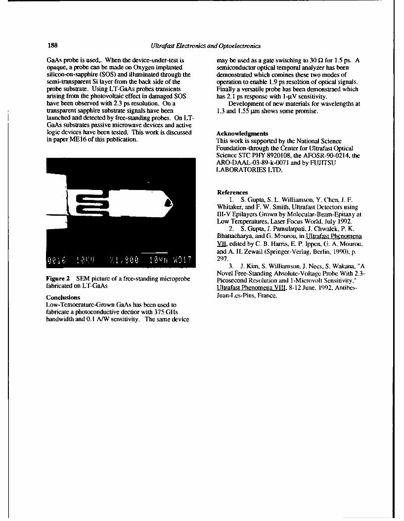
188 Ultrafast Electronics and Optoelectronics
GaAs probe is used,. When the device-under-test is may be used as a gate switching to 30 C1 for 1.5 ps. Aopaque, a probe can be made on Oxygen implanted semiconductor optical temporal analyzer has beensilicon-on-sapphire (SOS) and illuminated through the demonstrated which comines these two modes ofsemi-transparent Si layer from the back side of the operation to enable 1.9 ps resoltion of optical signals.probe substrate. Using LT-GaAs probes transients Finally a versatile probe has been demonstraed whicharising from the photovoltaic effect in damaged SOS has 2.1 ps response with 1-gtV sensitivity.have been observed with 2.3 ps resolution. On a Development of new materials for wavelengths attransparent sapphire substrate signals have been 1.3 and 1.55 pam shows some promise.launched and detected by free-standing probes. On LT-GaAs substrates passive microwave devices and activelogic devices have been tested. This work is discussed Acknowledgmentsin paper ME16 of this publication. This work is supported by the National Science
Foundation-through the Center for Ultrafast OpticalScience STC PHY 8920108, the AFOSR-90-0214, theARO-DAAL-03-89-k-0071 and by FUJITSULABORATORIES LTD.
References1. S. Gupta, S. L. Williamson, Y. Chen, J. F.
Whitaker, and F. W. Smith, Ultrafast Detectors usingIII-V Epilayers Grown by Molecular-Beam-Epitaxy atLow Temperatures, Laser Focus World, July 1992.
2. S. Gupta, J. Pamulatpati, J. Chwalek, P. K.Bhattacharya, and G. Mourou, in Ultrafast PhenomenaYllV edited by C. B. Harris, E. P. Ippen, G. A. Mourou,and A. 11. Zewail (Springer-Verlag, Berlin, 1990). p.297.
3. J. Kim, S. Williamson, J. Nees, S. Wakana, "ANovel Free-Standing Absolute-Voltage Probe With 2.3-
Figure 2 SEM picture of a free-standing microprobe Picosecond Resolution and 1 -Microvolt Sensitivity,"fabricated on LT-GaAs Ultrafast Phenomena VIII, 8-12 June, 1992, Antibes-
Conclusions Juan-Les-Pins, France.Low-Temoerature-Grown GaAs has been used tofabricate a photoconductive dectior with 375 GHsbandwidth and 0.1 A/W sensitivity. The same device
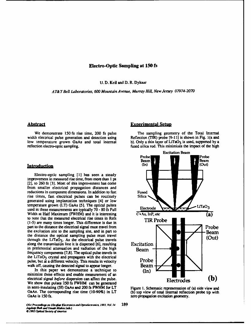
Electro-Optic Sampling at 150 fs
U. D. Keil and D. R. Dykaar
A T& T Bell Laboratories, 600 Mountain Avenue, Murray Hill, New Jersey 07974-2070
Abstract Exnerimental Setun
We demonstrate 150 fs rise time, 200 fs pulse The sampling geometry of the Total Internalwidth electrical pulse generation and detection using Reflection (TIR) probe 19-111 is shown in Fig. I (a andlow temperature grown GaAs and total internal b). Only a thin layer of LiTaO3 is used, supported by areflection electro-optic sampling, fused silica rod. This minimizes the impact of the high
Excitation BeamProbe1 ProbeBeam Beam
Itouto (In) (out)
Electro-optic sampling [1] has seen a steadyimprovement in measured rise time, from more than 1 ps[2], to 260 fs [3]. Most of this improvement has comefrom smaller electrical propagation distances andreductions in component dimensions. In addition to fast Fusedrise times, fast electrical pulses can be routinely Silicagenerated using implantation techniques [41 or lowtemperature grown (LT) GaAs [5]. The optical pulsesused in these measurements are typically 70 - 80 fs Full Electrode o-LiTaO3Width at Half Maximum (FWHM) and it is interesting C-AAs, InP, etc (a)to note that the measured electrical rise times in Refs M Probe(1-5) are many times longer. This difference is due inpart to the distance the electrical signal must travel from Probethe excitation site to the sampling site, and in part tothe distance the optical sampling pulse must travelthrough the LiTaO3 . As the electrical pulse travels (out)along the transmission line it is dispersed [61, resulting Excitationin preferential attenuation and radiation of the high Beamfrequency components [7,81. The optical pulse travels inthe LiTaO 3 crystal and propagates with the electricalpulse, but at a different velocity. This results in velocity Probewalk off, causing the detected signal to appear longer. Beam
In this paper we demonstrate a technique to (In)minimize these effects and enable measurement of anelectrical signal before dispersion can affect the pulse. Electrodes (b)We show that pulses 250 fs FWHM can be generatedin semi-insulating (SI) GaAs and 200 fs FWHM for LT Figure 1. Schematic representation of (a) side view andGaAs. The corresponding rise time (10-90%) in LT (b) top view of total internal reflection probe tip withGaAs is 150 fs. zero propagation excitation geometry.
OSA PNocenp on• UkrOW Ek op csad oekot Vvu 1993. Vol. 4 189Jqdte SNu a• d UmA MVu (e*&)01993 OpjwSod if qAntalooz
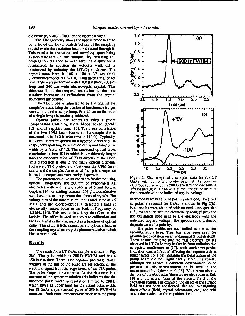
190 Ultrafast Electronics and Optoelectronics
dielectric (er > 40) LiTaO3 on the electrical signal. 1.2 (a) ....
The TIR geometry allows the optical probe beam to
be reflected off the (uncoated) bottom of the sampling 1.0crystal while the excitation beam is directed through it.This results in excitation and sampling spots being -0.8superimposed on the sample. By reducing thepropagation distance to near zero the dispersion is >00.6 200 fs FWHMminimized. In addition the velocity walk off isminimized by reducing the LiTaO3 thickness. The " 0.4crystal used here is 100 x 100 x 37 pim thick(Terametrics model 200B-TIR). Data taken for a longer w'0.2time range were performed with a 100 pm thick, 200 pmn 0long and 300 pum wide electro-optic crystal. This 0.0 ........thickness limits the temporal resolution but the timewindow increases as reflections from the crystal -0.2 .boundaries are delayed. 0.0 0.5 1.0 1.5 2.0 2.5
The TIR probe is adjusted to be flat against the Time (ps)sample by minimizing the number of interference fringes Jseen with the microscope lamp. Parallelism on the order 6of a single fringe is routinely achieved. (b)
Optical pulses are generated using a prism 5- +10Vcompensated Colliding Pulse Mode-locked (CPM)[12] and Ti:Sapphire laser [131. The cross correlation ,-of the two CPM laser beams at the sample site ismeasured to be 160 fs (rise time is 110 fs). Typically, 3autocorrelations are quoted for a hyperbolic secant pulse 2shape, corresponding to reduction of the measured pulsewidth by a factor of 1.5. The corrected optical cross -10Vcorrelation is then 105 fs which is considerably longerthan the autocorrelation of 70 fs directly at the laser.This dispersion is due to the many optical elements(polarizer, TIR probe, etc.) between the CPM laser 10 15 20 a- U 3.cavity and the sample. An external four pfism sequence Tine (ps)is used to compensate extra-cavity dispersion.
The photoconductive switches are fabricated using Figure 2. Electro-optically sampled data for (a) LToptical lithography and 500 nm of evaporated Au GaAs with pump and probe beam at the positiveelectrodes with widths and spacing of 5 and 10 gin. electrode (pulse width is 200 fs FWHM and rise time isGaplestrodes [1] o iding cntspactng 1151 phtcnductive 15.9 fs) and (b) SI GaAs with pump and probe beam atGapless [141 or sliding contact [151 photoconductive the electrode with the indicated applied voltage.switches are used to generate the electrical signals. Thevoltage bias of the transmission line is modulated at 3.5 and probe beam next to the positive electrode. The effectMHz and the electro-optically detected signal is of polarity reversal for GaAs is shown in Fig 2(b).electrically mixed down to the lock-in frequency of Both results were obtained with an excitation spot size1.2 kHz [16]. This results in a large dc offset on the (-3 gm) smaller than the electrode spacing (5 lum) andlock-in. The offset is used as a voltage calibration and the excitation spot next to the electrode with thethe fast signal is then measured as a function of optical indicated applied voltage. The spectra show a drasticdelay. This setup selects against purely optical effects in dependence on the polarity.the sampling crystal as only the photoconductive switch The pulse widths are not limited by the carrierbias is modulated. recombination time. This has also been seen for
asymmetric excitation on an undamaged Si substrate[3].These results indicate that the fast electrical pulses
Results observed in LT GaAs may in fact be from radiation dueto optical nonlinearities [171, with carrier properties
The result for a LT GaAs sample is shown in Fig. (i.e., short carrier lifetime) affecting the response only at2(a). The pulse width is 200 fs FWHM and has a longer times ( > 1 ps). Rotating the polarization of the150 fs rise time. There is no negative pre-pulse. Small pump beam did not significantly affect the result.,wiggles in the tail of the pulse are reflections of the although we expect a coherent contribution to beelectrical signal from the edge facets of the TIR probe. present in this measurement as is seen in theThe pulse shape is symmetric. As the rise time is a measurement by Dyk'ir, et al 1181. What is not clear is
the role of the eloctrodes (there are no electrodes in Ref.measure of the system resolution this indicates that the 18) and the actual form of the electric field in theobserved pulse width is resolution limited to 200 fs excitation region. For example, the effect of the surfacewhich gives an upper limit for the actual pulse width. field has not been considered. We are investigatingFor SI GaAs a symmetrical pulse of 250 fs FWHM is these effects (field, crystal orientation, etc.) and willmeasured. Both measurements were made with the pump report the results in a future publication.
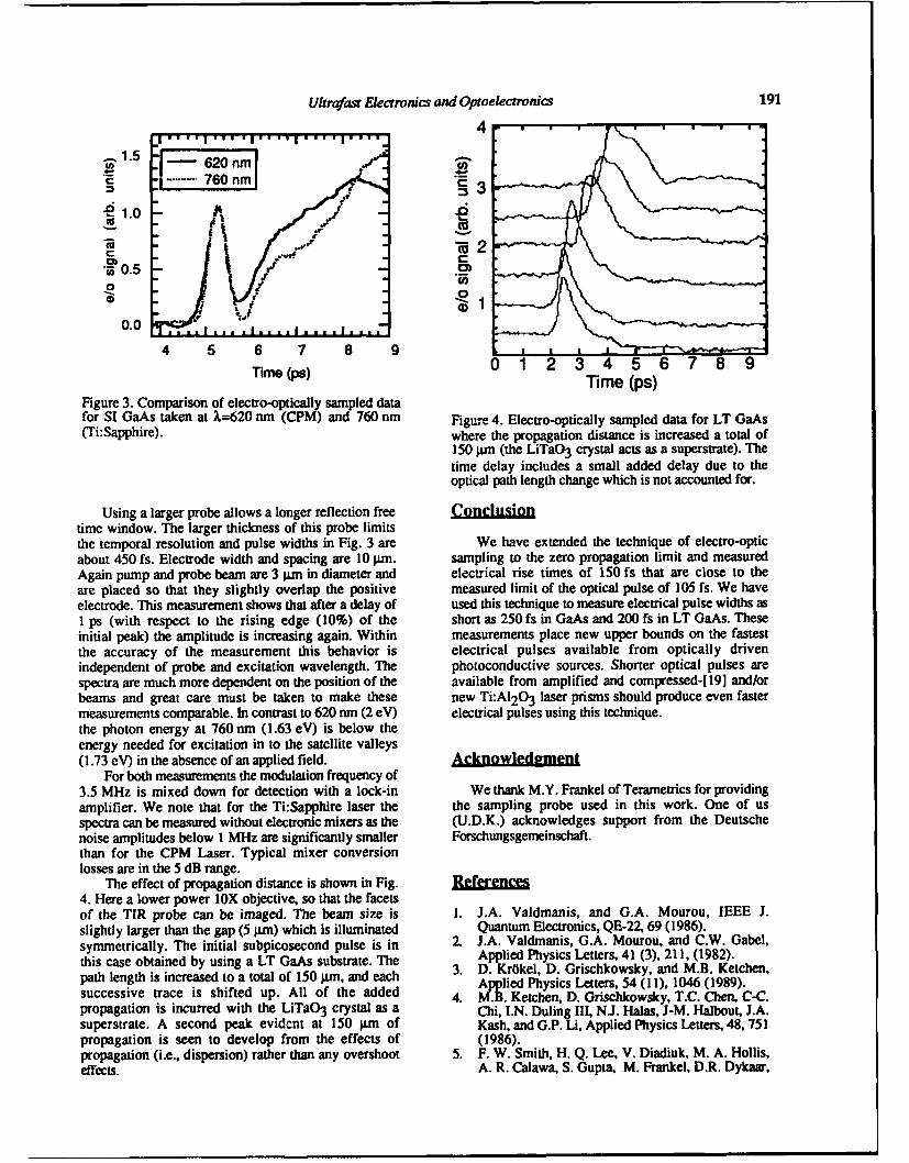
Ultrafast Elekaronics and Optoelectronics 191
- 1.5 620 nm""E 760 nm " 3
1.0o
Tim (ps
CO
.F
o / 0
0.0 '- fg s1 24 5 6 7 8 9
Time ~Time (ps)Figure 3. Comparison of electro-optically sampled datafor SI GaAs taken at X=620 anm (CPM) and 760 nm Figure 4. Electro-optically sampled data for LT GaAs(Ti:Sapphire). where the propagation distance is increased a total of
150 pim (the LiTaO3 crystal acts as a superstrate). Thetime delay includes a small added delay due to theoptical path length change which is not accounted for.
Using a larger probe allows a longer reflection free Cncsiontime window. The larger thickness of this probe limitsthe temporal resolution and pulse widths in Fig. 3 are We have extended the technique of electro-opticabout 450 fs. Electrode width and spacing are 10 ;im. sampling to the zero propagation limit and measuredAgain pump and probe beam are 3 plm in diameter and electrical rise times of 150 fs that are close to theare placed so that they slightly overlap the positive measured limit of the optical pulse of 105 fs. We haveelectrode. This measurement shows that after a delay of used this technique to measure electrical pulse widths as1 ps (with respect to the rising edge (10%) of the short as 250 fs in GaAs and 200 fs in LT GaAs. Theseinitial peak) the amplitude is increasing again. Within measurements place new upper bounds on the fastestthe accuracy of the measurement this behavior is electrical pulses available from optically drivenindependent of probe and excitation wavelength. The photoconductive sources. Shorter optical pulses arespectra are much more dependent on the position of the available from amplified and compressed-[ 19] and/orbeams and great care must be taken to make these new Ti:A12 03 laser prisms should produce even fastermeasurements comparable. In contrast to 620 nrm (2 eV) electrical pulses using this technique.the photon energy at 760 nm (1.63 eV) is below theenergy needed for excitation in to the satellite valleys(1.73 eV) in the absence of an applied field. AcknowiedIment
For both measurements the modulation frequency of3.5 MHz is mixed down for detection with a lock-in We thank M.Y. Frankel of Terametrics for providingamplifier. We note that for the Ti:Sapphire laser the the sampling probe used in this work. One of usspectra can be measured without electronic mixers as the (U.D.K.) acknowledges support from the Deutschenoise amplitudes below 1 MHz are significantly smaller Forschungsgemeinschaft.than for the CPM Laser. Typical mixer conversionlosses are in the 5 dB range.
The effect of propagation distance is shown in Fig. References4. Here a lower power lOX objective, so that the facetsof the TIR probe can be imaged. The beam size is 1. J.A. Valdmanis, and G.A. Mourou, IEEE J.slightly larger than the gap (5 jim) which is illuminated Quantum Electronics, QE-22, 69 (1986).symmetrically. The initial subpicosecond pulse is in 2. J.A. Valdmanis, G.A. Mourou, and C.W. Gabel,this case obtained by using a LT GaAs substrate. The Applied Physics Letters, 41 (3), 211, (1982).
path length is increased to a total of 150 gm, and each 3. D. KrJkel, D. Grischkowsky, and M.B. Ketchen,
successive trace is shifted up. All of the added Applied Physics Letters, 54 (11), 1046 (1989).4. M.B. Ketchen, D. Grischkowsky, T.C. Chen, C-C.
propagation is incurred with the LiTaO3 crystal as a Chi, I.N. Duling Il, NJ. Halas, J-M. Halbout, J.A.superstrate. A second peak evidcnt at 150 1.m of Kash, and G.P. Li, Applied Physics Letters, 48, 751propagation is seen to develop from the effects of (1986).propagation (i.e., dispersion) rather than any overshoot 5. F. W. Smith, H. Q. Lee, V. Diadiuk, M. A. Hollis,effects. A. R. Calawa, S. Gupta, M. Frankel, D.R. Dykaar,
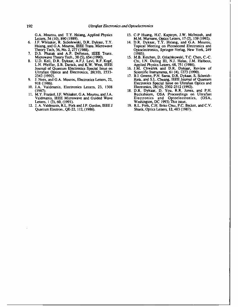
192 Ultrafast Electronics and Optoelectronics
G.A. Mourou, and T.Y. Hsiang, Applied Physics 13. C-P Huang, H.C. Kapteyn, J.W. McIntosh, andLetters, 54 (10), 890 (1989). M.M. Murnane, Optics Letters, 17 (2), 139 (1992).
6. J.F. Whitaker, R. Sobolewski, D.R. Dykaar, T.Y. 14. D.R. Dykaar, T.Y. Hsiang, and G.A. Mourou,Hsiang, and G.A. Mourou, IEEE Trans. Microwave Topical Meeting on Picosecond Electronics andTheory Tech, 36, No. 2, 277 (1988). Optoelectronics, Springer-Verlag, New York, 249
7. D.S. Phatak and A.P. Defonzo, IEEE Trans. (1985).Microwave Theory Tech., 38 (5), 654 (1990). 15. M.B. Ketchen, D. Grischkowski, T.C. Chen, C.-C.
8. U.D. Keil, D.R. Dykaar, A.FJ. Levi, R.F. Kopf, Chi, I.N. Duling III, N.J. Halas, J.M. Halbout,L.N. Pfeiffer, S.B. Darack, and K.W. West, IEEE Applied Physics Letters, 48, 751 (1986).Journal of Quantum Electronics Special Issue on 16. J.M. Chwalek and D.R. Dykaar, Review ofUltrafast Optics and Electronics, 28(10), 2333- Scientific Instruments, 61 (4), 1273 (1990).2342 (1992). 17. B.I. Greene, P.N. Saeta, D.R. Dykaar, S. Schmidt-
9. J. Nees, and G.A. Mourou, Electronics Letters, 22, Rink, and S.L. Chuang, IEEE Journal of Quantum918 (1986). Electronics Special Issue on Ultrafast Optics and
10. J.A. Valdmanis, Electronics Letters, 23, 1308 Electronics, 28(10), 2302-2312 (1992).(1987). 18. D.R. Dykaar, D. You, R.R. Jones, and P.H.
11. M.Y. Frankel, J.F. Whitaker, G.A. Mourou, and J.A. Bucksbaum, OSA Proceedings on UltrafastValdmanis, IEEE Microwave and Guided Wave Electronics and Optoelectronics, (OSA,Letters, 1 (3), 60, (1991). Washington, DC 1993) This issue.
12. J. A. Valdmanis, R.L. Fork and J.P. Gordon, IEEE J 19. R.L. Fork, C.H. Brito Cruz, P.C. Becker, and C.V.Quantum Electron., QE-22, 112, (1986). Shank, Optics Letters, 12, 483 (1987).
Low-Temperature MBE Growth of HI-V Materials onSi Substrates
Michael Y. Frankel and Thomas F. CarruthersOptical Sciences Division, CODE 5672, Naval Research Laboratory,
Washington, DC 20375-5338
Bijan TadayonElectronic Technology Division, Naval Research Laboratory, Washington, DC 203 75-5338
Abstract In this work we investigate the influence of theMBE growth temperature and post-growth anneal on the
We investigate the molecular-beam epitaxial (MBE) photogenerated carrier lifetime, carrier mobility, andgrowth of GaAs and In0 .6Ga0 .4 As on Si substrates at resistivity in GaAs and ln0.6Ga0.4As epitaxially grownlow substrate temperatures. Such materials may allow on Si substrates. We use femtosecond time-resolveddirect integration of ultrafast photodetectors into Si- surface reflectivity measurements to show that abased integrated circuits. Femtosecond time-resolved reduction in carrier lifetime from 14 ps to <0.5 ps cansurface reflectivity and photoconductor switching are be achieved in LT GaAs by reducing the growthused to explore material photonic properties. We temperature from 400 "C to 150 "C, and from 10 ps toobserve free carrier lifetimes as short as <500 fs and <0.4 ps in LT In0 .6Ga 0.4 As by reducing the growthphotoconductor electrical responses as short as 600 fs. temperature from 350 "C to 150 *C. We fabricate
photoconductor switches and use electrooptic (EO)sampling to measure their electrical bandwidth and
Introduction responsivity. We demonstrate that reduced MBE growthtemperature results in sub-picosecond measured impulse
Si-based integrated circuits still play a significant role response, with some sacrifice in carrier mobility.in modern communication systems. However, efficient Furthermore, the significant influence of post-growthand fast Si-based photodetectors are not available at the anneal on material properties is demonstrated.important 1.3-pm and 1.5-jim wavelengths. Manycommunication systems could benefit from the directintegration of Ill/V-semiconductor-based photodetectors Experimentinto Si circuits due to their increased bandwidth andlong-wavelength sensitivity. The 1-pm-thick layers of GaAs were MBE-grown on
Typically, the performance of devices fabricated in (100) Si substrates at several substrate temperatures.III-V materials grown on Si substrates suffers due to a After cleaning in a 2:25 H:DI solution for 20 s, thehigh defect density induced by the lattice mismatch [I]. substrates were loaded into the MBE chamber and heatedIlowever, this reduction in carrier lifetime can be used to.640 "C to remove some residual oxide. The materialto advantage for high-speed photodetectors [2]. Low- was grown at a 0.5-pm/hr growth rate with an As/Gatemperature (LT) MBE growth can result in further equivalent beam-pressure ratio of 30. Half of eachimprovements, and LT GaAs grown on GaAs has sample was subsequently cleaved off and annealed atshown excellent optoclectronic properties such as subpi- 610 "C for 10 min under As overpressure. A set ofcosccond carrier lifetime, high mobility and high coplanar wavcguide transmission lines (CPW) with aresistivity [3]. Such LT GaAs has been applied for 20-pro center conductor, 20-jm conductor spacing and ahigh-sensitivity, ultrafast metal-semiconductor-metal 15-jim embedded photoconductor gap switch wasphotodetectors [4-6], and for high-voltage switching fabricated on each sample.applications [7,81. Also, InGaAs grown on GaAs has Similarly, the 0.56-jim-thick layers of In0fGao.4Asshown potential for optoelectronic applications at were MBE-grown on (100) Si substrates at severallonger wavelengths [9]. substrate temperatures. An identical set of CPWs was
OSA Proceaan on *4A Ekfro and Opuolecnomkz 193, Vol. 14 193Jagdeep Vah aid timeA Mhha (ak)1993 Opdcda Sdiety qAmui1ca
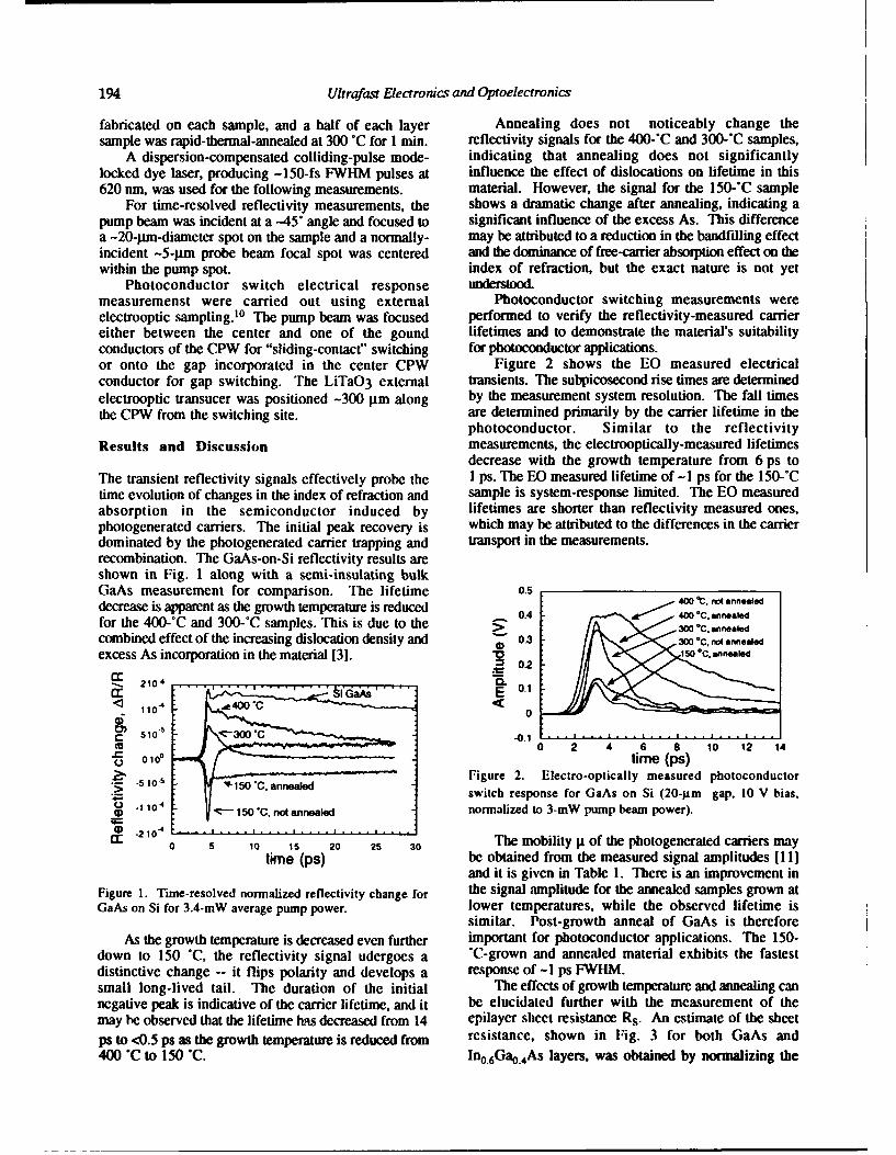
194 Ultrafast Electronics and Optoelectronics
fabricated on each sample, and a half of each layer Annealing does not noticeably change thesample was rapid-thermal-annealed at 300 'C for I min. reflectivity signals for the 400-'C and 300-*C samples,
A dispersion-compensated colliding-pulse mode- indicating that annealing does not significantlylocked dye laser, producing -150-fs FWHM pulses at influence the effect of dislocations on lifetime in this620 un, was used for the following measurements. material. However, the signal for the 1 50-'C sample
For time-resolved reflectivity measurements, the shows a dramatic change after annealing, indicating apump beam was incident at a -45* angle and focused to significant influence of the excess As. This differencea -20-jim-diameter spot on the sample and a normally- may be attributed to a reduction in the bandfilling effectincident -5-jim probe beam focal spot was centered and the dominance of free-carrier absorption effect on thewithin the pump spot. index of refraction, but the exact nature is not yet
Photoconductor switch electrical response understood-measuremenst were carried out using external Photoconductor switching measurements wereelectrooptic sampling.10 The pump beam was focused performed to verify the reflectivity-measured carriereither between the center and one of the gound lifetimes and to demonstrate the material's suitabilityconductors of the CPW for "sliding-contact" switching for photoconductor applications.or onto the gap incorporated in the center CPW Figure 2 shows the EO measured electricalconductor for gap switching. The LiTaO3 external transients. The subpicosecond rise times are determinedelectrooptic transucer was positioned -300 gim along by the measurement system resolution. The fall timesthe CPW from the switching site. are determined primarily by the carrier lifetime in the
photoconductor. Similar to the reflectivityResults and Discussion measurements, the electrooptically-measured lifetimes
decrease with the growth temperature from 6 ps toThe transient reflectivity signals effectively probe the 1 ps. The EO measured lifetime of -1 ps for the 150-'Ctime evolution of changes in the index of refraction and sample is system-response limited. The EO measuredabsorption in the semiconductor induced by lifetimes are shorter than reflectivity measured ones,photogenerated carriers. The initial peak recovery is which may be attributed to the differences in the carrierdominated by the photogenerated carrier trapping and transport in the measurements.recombination. The GaAs-on-Si reflectivity results areshown in Fig. I along with a semi-insulating bulkGaAs measurement for comparison. The lifetime 0.5
decrease is apparent as the growth temperature is reduced 0.4 . C ., a.,eled
for the 400-C and 300-°C samples. This is due to the >"combined effect of the increasing dislocation density and 0.3 300*c, ntanea• •excess As incorporation in the material [3]. "5 *.a
2t104 0Lcc IGa~sE 0.1
110400 060
CU-4 - ' 0 2 4 6 8 10 12 14o1•0 time (ps)
•ý .-- 0 -"Figure 2. Electro-optically measured photoconductor•> rswitch response for GaAs on Si (20-jim gap, 10 V bias,
- 104 -- 15o "C, not annealed normalized to 3-mW pump beam power).
0c 6 10 1 20 26 30 The mobility It of the photogenerated carriers maytime (ps) be obtained from the measured signal amplitudes [I
and it is given in Table I. There is an improvement inFigure 1. Time-resolved normalized reflectivity change for the signal amplitude for the annealed samples grown atGaAs on Si for 3.4-mW average pump power. lower temperatures, while the observed lifetime is
similar. Post-growth anneal of GaAs is thereforeAs the growth temperature is decreased even further important for photoconductor applications. The 150-
down to 150 "C, the reflectivity signal udergoes a 'C-grown and annealed material exhibits the fastestdistinctive change -- it flips polarity and develops a response of -I ps FWtlM.small long-lived tail. The duration of the initial The effects of growth temperature and annealing cannegative peak is indicative of the carrier lifetime, and it be elucidated further with the measurement of themay be observed that the lifetime has decreased from 14 epilayer sheet resistance Rs. An estimate of the sheetps to <0.5 ps as the growth temperature is reduced from resistance, shown in Fig. 3 for both GaAs and400 "C to 150 C. In 0 .6Gao.4As layers, was obtained by normalizing the
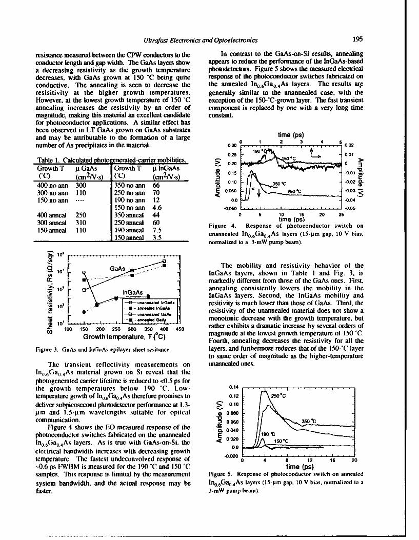
Ultrafast Electronics and Optoelectronics 195
resistance measured between the CPW conductors to the In contrast to the GaAs-on-Si results, annealingconductor length and gap width. The GaAs layers show appears to reduce the performance of the InGaAs-baseda decreasing resistivity as the growth temperature photodetectors. Figure 5 shows the measured electricaldecreases, with GaAs grown at 150 "C being quite response of the photoconductor switches fabricated onconductive. The annealing is seen to decrease the the annealed In0 .Ga 0 .4 As layers. The results ar~eresisitivity at the higher growth temperatures. generally similar to the unannealed case, with theHowever, at the lowest growth temperature of 150 TC exception of the 150-*C-grown layer. The fast transientannealing increases the resistivity by an order of component is replaced by one with a very long timemagnitude, making this material an excellent candidate constant.for photoconductor applications. A similar effect hasbeen observed in LT GaAs grown on GaAs substratesand may be attributable to the formation of a large time (ps)
number of As precipitates in the material. 0.30 0 ... , . , ... , 0.02
Table 1. Calculated photoo nerated-carrier mobilities. 025 - o 0
Growth T p GaAs Growth T p InGaAs "D"00.15 • -f -0oO4.01
(C) (c 2 N2 s) ('C) (cm 2/V.s) -, 00o.10 -5=: -0.02 CL
400 no ann 300 350 no ann 66 35 -0.0
300 no ann 110 250 no ann 70 E 0. 0.03
150 no ann ... 90 no ann 12 0.0- o.04150 no ann 4.6 .050 ... 05
400 anneal 250 350 anneal 44 0 5 10 15 20 25
300 anneal 310 250 anneal 60 time (ps)150anneal 110 190annel 7.5 Figure 4. Response of photoconductor switch on
0190 anneal 7.5 unannealed Ino0 6Gao.4As layers (15-lm gap, 10 V bias,normalized to a 3-mW pump beam).
Z'
lO The mobility and resistivity behavior ol theA ... InGaAs layers, shown in Table 1 and Fig. 3, isM .markedly different from those of the GaAs ones. First,f 1o annealing consistently lowers the mobility in the• InGaAs layers. Second, the lnGaAs mobility and
1 0o3 -0- una-- InGA resitivity is much lower than those of GaAs. Third, the
13 uIl e_, W, GaAs resistivity of the unannealed material does not show aD o 2. _I . monotonic decrease with the growth temperature, but
- 10 3C 350 400 450 rather exhibits a dramatic increase by several orders ofSGrowth temperature, T c) magnitude at the lowest growth temperature of 150 'C.
Fourth, annealing decreases the resistivity for all theFigure 3. GaAs and InGaAs epilayer sheet resitance. layers, and furthermore reduces that of the 150-'C layer
to same order of magnitude as the higher-temperatureThe transient reflectivity measurements on unannealed ones.
Ino.6Gao. 4As material grown on Si reveal that thephotogeneratcd carrier lifetime is reduced to <0.5 ps forthe growth temperatures below 190 *C. Low- 0.14
temperature gowth of lno 6Ga0.4As therefore promises to 0.12 - 250C
deliver subpicosecond photodetector performance at 1.3- > 0.l0 -min and 1.5-pm wavelengths suitable for optical 0 o.0oo
communication. 1 .060 - 35o CFigure 4 shows the 1O measured response of the 0 .040
photoconductor switches fabricated on the unannealcd 190 1C
In0.6Gao.4As layers. As is true with GaAs-on-Si, the 000 150oC
electrical bandwidth increases with decreasing growthtemperature. The fastest undcconvolved response of .0.0o 0 4 8 12 16 20
-0.6 ps FWIIM is measured for the 190 "C and 150 TC time (ps)samples. ibis response is limited by the measurement Figure 5. Response of photoconductor switch on annealedsystem bandwidth, and the actual response may be in0.6GaO. 4As layers (15-1m gap. 10 V bias, normalized to afaster. 3-mW pump beam).
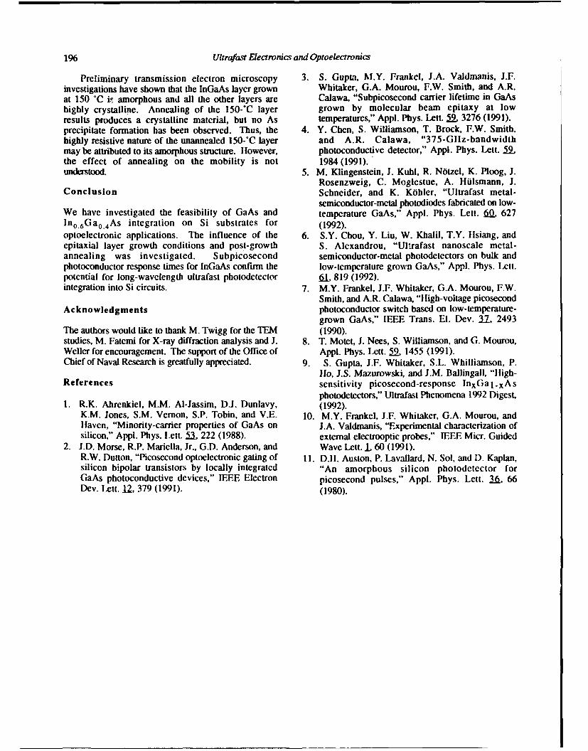
196 Ultrafast Electronics and Optoelectronics
Preliminary transmission electron microscopy 3. S. Gupta, M.Y. Frankel, J.A. Valdmanis, J.F.investigations have shown that the InGaAs layer grown Whitaker, G.A. Mourou, F.W. Smith, and A.R.at 150 "C i! amorphous and all the other layers are Calawa, "Subpicosecond carrier lifetime in GaAshighly crystalline. Annealing of the 150-*C layer grown by molecular beam epitaxy at lowresults produces a crystalline material, but no As temperatures," Appl. Phys. Lett. 59. 3276 (1991).precipitate formation has been observed. Thus, the 4. Y. Chen, S. Williamson, T. Brock, F.W. Smith,highly resistive nature of the unannealed 150-°C layer and A.R. Calawa, "375-Gllz-bandwidthmay be attributed to its amorphous structure. llowever, photoconductive detector," Appl. Phys. Lett. 59.the effect of annealing on the mobility is not 1984 (1991).understood. 5. M. Klingenstein, J. Kuhl, R. Notzel, K. Ploog, J.
Rosenzweig, C. Moglestue, A. HUlsmann, J.Conclusion Schneider, and K. Kohler, "Ultrafast metal-
semiconductor-metal photodiodes fabricated on low-We have investigated the feasibility of GaAs and temperature GaAs," Appl. Phys. Lett. 60. 627In 0 .6Ga 0 .4As integration on Si substrates for (1992).optoelectronic applications. The influence of the 6. S.Y. Chou, Y. Liu, W. Khalil, T.Y. Hlsiang, andepitaxial layer growth conditions and post-growth S. Alexandrou, "Ul.rafast nanoscale metal-annealing was investigated. Subpicosecond semiconductor-metal photodetectors on bulk andphotoconductor response times for InGaAs confirm the low-temperature grown GaAs," Appl. Phys. Lcit.potential for long-wavelength ultrafast photodetector 1, 819 (1992).integration into Si circuits. 7. M.Y. Frankel, J.F. Whitaker, G.A. Mourou, F.W.
Smith, and A.R. Calawa, "Hligh-voltage picosecondAcknowledgments photoconductor switch based on low-temperature-
grown GaAs," IEEE Trans. El. Dev. 31, 2493The authors would like to thank M. Twigg for the TEM (1990).studies, M. Fatemi for X-ray diffraction analysis and J. 8. T. Motet, J. Nees, S. Williamson, and G. Mourou,Weller for encouragement. The support of the Office of Appl. Phys. Lett. a9. 1455 (1991).Chief of Naval Research is greatfully appreciated. 9. S. Gupta, J.F. Whitaker, S.L. Whilliamson, P.
HIo, J.S. Mazurowski, and J.M. Ballingall, "tligh-References sensitivity picosecond-response InxGalxAs
photodetectors," Ultrafast Phenomena 1992 Digest,1. R.K. Ahrenkiel, M.M. AI-Jassim, D.J. Dunlavy, (1992).
K.M. Jones, S.M. Vernon, S.P. Tobin, and V.E. 10. M.Y. Frankel, J.F. Whitaker, G.A. Mourou, andHaven, "Minority-carrier properties of GaAs on J.A. Valdmanis, "Experimental characterization ofsilicon," Appl. Phys. Lett. 5 222 (1988). external electrooptic probes," IEEE Micr. Guided
2. J.D. Morse, R.P. Mariella, Jr., G.D. Anderson, and Wave Lett. 1. 60 (1991).R.W. Dutton, "Picosecond optoelectronic gating of 11. D.11. Auston, P. Lavallard, N. Sol, and D. Kaplan,silicon bipolar transistors by locally integrated "An amorphous silicon photodetector forGaAs photoconductive devices," IEEE Electron picosecond pulses," Appi. Phys. Lett. 3A, 66Dev. Lett. 12, 379 (1991). (1980).
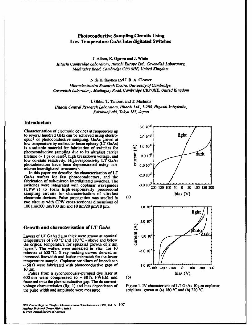
Photoconductive Sampling Circuits UsingLow-Temperature GaAs Interdigitated Switches
J. Allam, K. Ogawa and J. WhiteHitachi Cambridge Laboratory, Hitachi Europe Lid, Cavendish Laboratory,
Madingley Road, Cambridge CB3 OHE, United Kingdom
N.de B. Baynes and 1. R. A. CleaverMicroelectronics Research Centre, University of Cambridge,
Cavendish Laboratory, Madingley Road, Cambridge CB3"OHF United Kingdom
L Ohbu, T. Tanoue, and T. MishimaHitachi Central Research Laboratory, Hitachi Ltdi, 1-280, Higashi-koigakubo,
Kokubunji-shi, Tokyo 185, Japan
Introduction3.0 1 .. .. .. .. .. .. ..
Characterisation of electronic devices at frequencies upto several hundred GHz can be achieved using electro- 2.0 10- lightoptic1 or photoconductive sampling. GaAs grown atlow temperature by molecular beam epitaxy (LT GaAs) 1.0 'sis a suitable material for fabrication of switches for 1.0 10photoconductive sampling due to its ultrafast carrierlifetime (~ 1 ps or less)2, high breakdown voltage, and • 0.0 10° ~i
low on-state resistivity. High-responsivity LT GaAsphotodetectors have been demonstrated using sub- -1.0 5micron interdigitated structures 3.
In this paper we describe the characterisation of LT -2.0 l0rsGaAs wafers for fast photoconductors, and thefabrication of sub-micron interdigitated switches. Thesw itches w ere integrated w ith coplanar w aveguides -3.0 I 1f..0..150 .10
(CPW's) to form high responsivity picosecond 00-150-100 -50 0 50 100 150 200sampling circuits for characterisation of ultrafast biaselectronic devices. Pulse propagation was studied in (a)two circuits with CPW cross-sectional dimensions of100 pmf200 pm/10O pm and 10 pm/20 pm/10 ;zm. 1.0 10. .
lightg
95.0 I0~y5
Growth and characterisation of LT GaAs 5.o
Layers of LT GaAs 2 pm thick were grown at nominal 0.0 1(1'temperatures of 220 *C and 180 *C - above and below
the critical temperature for epitaxial growth of 2 pmlayers4 . The wafers were annealed in situ for 10 -5.005minutes at 600 *C. X-ray rocking curves showed anincreased linewidth and lattice mismatch for the lowertemperature sample. Coplanar striplines of impedance-50 0 were fabricated with photoconductive gaps of -1.0 10 0-4 ... 0 .........
10ules from a synchronously-pumped dye laser at bias (V)
600 nm were compressed to - 80 fs FWHM and (b)focussed onto the photoconductive gap. The dc current-voltage characteristics (fig. 1) and bias dependence of Figure 1. IV characteristic of LT GaAs 10 W coplanarthe pulse width and amplitude were measured. striplines, grown at (a) 180 *C and (b) 220 *C.
OSA Proceedngs on Ukraf•As Liekronks and Opeoelectronki 1993. VoL 14 197Jagdeep Shah and Umesh Mishra (eds)0 1993 Optical Society ofAmerica
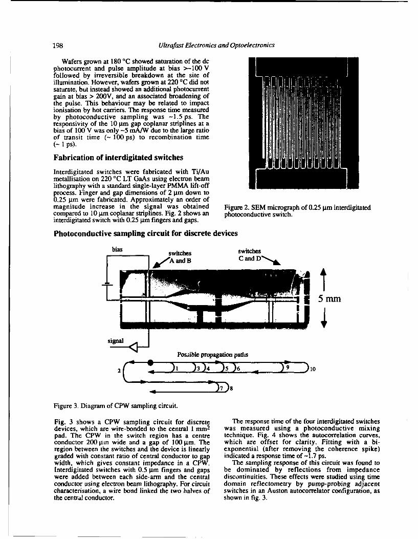
198 Ultrafast Electronics and Optoelectronics
Wafers grown at 180 °C showed saturation of the dcphotocurrent and pulse amplitude at bias >-100 Vfollowed by irreversible breakdown at the site ofillumination. However, wafers grown at 220 °C did notsaturate, but instead showed an additional photocurrentgain at bias > 200V, and an associated broadening ofthe pulse. This behaviour may be related to impactionisation by hot carriers. The response time measuredby photoconductive sampling was -1.5ps. Theresponsivity of the 10 •tm gap coplanar striplines at abias of 100 V was only ~5 mA/W due to the large ratioof transit time (-100 ps) to recombination time(~ 1 ps).
Fabrication of interdigitated switches
Interdigitated switches were fabricated with Ti/Aumetallisation on 220 °C LT GaAs using electron beamlithography with a standard single-layer PMMA lift-offprocess. Finger and gap dimensions of 2 Ixm down to0.25 •tm were fabricated. Approximately an order ofmagnitude increase in the signal was obtained Figure2. SEMmicrographof0.25 •minterdigitatedcompared to 10 •tm coplanar striplines. Fig. 2 shows an photoconductive switch.interdigitated switch with 0.25 •tm fingers and gaps.
Photoconductive sampling circuit for discrete devices
bias switches switches•/A and B C and D'•L
S.SJ
signal
----<b-Possible propagation paths
- ")7)s
Figure 3. Diagram of CPW sampling circuit.
Fig. 3 shows a CPW sampling circuit for discrete The response time of the four interdigitated switchesdevices, which are wire-bonded to the central 1 ram2 was measured using a photoconductive mixingpad. The CPW in the switch region has a centre technique. Fig. 4 shows the autocorrelation curves,conductor 200 •m wide and a gap of I00 ttm. The which arc offset for clarity. Fitting with a hi-region between the switches and the device is linearly exponential (after removing the coherence spike)graded with constant ratio of central conductor to gap indicated a response time of -1.7 ps.width, which gives constant impedance in a CPW. The sampling response of this circuit was found toInterdigitated switches with 0.5 •tm fingers and gaps be dominated by reflections from impedancewere added between each side-ann and the central discontinuities. These effects were studied using timeconductor using electron beam lithography. For circuit domain reflectometry by pump-probing adjacentcharacterisation, a wire bond linked the two halves of switches in an Auston autocorrelator configuration, asthe central conductor, shown in fig. 3.
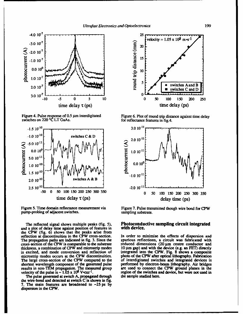
Ultrafast Electronics and Optoelectronics 199
-4.0 10 .7. 25velocity 1.05x10 8 m-s
-3.0 10.-
-2.0 107
-7 15-1.0 10 15
0.0160i .o lO0 lS10 10710
A 2.0 10-7 1
2.0 1077 switches Aand B2.0 2 *switches Cand D
3.0 10.7 ......... 0-10 -5 0 5 10 0 50 100 150 200 250
time delay x (ps) time delay (ps)
Figure 4. Pulse response of 0.5 gm interdigitated Figure 6. Plot of round trip distance against time delayswitches on 220 °C LT GaAs. for reflectance features in fig.4.
-1.5 10-.0 ... 3.0 10-"1
-1.0 10.107 switches C & D2.0 10.11-
-5.0 10.11
S0 .0 10.0 1.0 10"1
5.0 10"- ,
S1.5 10"10 :-" '. 1 02.0.01100 0
1.510--1.0 10"12.0 10-10 switches A & B
2.5 10I°0 .......... ...................... -2.0 10 11 ...
-50 0 50 100 150 200 250 300 350 0 50 I00 150 20 250 300 350time delay T (ps) delay time (ps)
Figure 5. Time domain reflectance measurement via Figure 7. Pulse transmitted though wire bond for CPWpump-probing of adjacent switches. sampling substrate.
The reflected signal shows multiple peaks (fig. 5), Photoconductive sampling circuit integratedand a plot of delay time against position of features in with device.the CPW (fig. 6) shows that the peaks arise fromreflection at discontinuities in the CPW cross-section. In order to minimise the effects of dispersion andThe propagation paths are indicated in fig. 3. Since the spurious reflections, a circuit was fabricated withcross-section of the CPW is comparable to the substrate reduced dimensions (20 gm centre conductor andthickness, a combination of CPW and microstrip modes 10 pm gap) and with the device (e.g. an FEr) directlyis excited, and mode conversion and reflection of integrated into the CPW. Fig. 8 shows a compositemicrostrip modes occurs at the CPW discontinuities. photo of the CPW after optical lithography. FabricationThe large cross-section of the CPW compared to the of interdigitated switches and integrated devices isshortest wavelength component of the generated pulse performed by electron-beam lithography. Air bridgesresults in non-TEM propagation. The measured group are used to connect the CPW ground planes in thevelocity of the pulse is - 1.05 x 10⁸ V-cm-1. region of the switches and device, but were not used in
The pulse generated at switch A, propagated through the sample studied here.the wire-bond and detected at switch C is shown in fig.7. The main features are broadened to -25 ps bydispersion in the CPW.
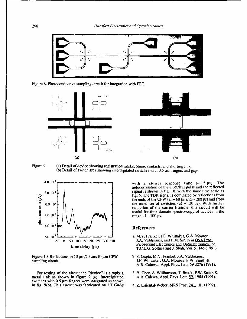
200 Ultrafast Electronics and Optoelectronics
Figure 8. Photoconductive sampling circuit for integration with FET.
I.-
(a) (b)
Figure 9. (a) Detail of device showing registration marks, ohmic contacts, and shorting link.(b) Detail of switch area showing interdigitated switches with 0.5 gtm fingers and gaps.
-4.0 10-8. with a slower response time (- 15 ps). Theautocorrelation of the electrical pulse and the reflected
-2.0 10-8 signal is shown in fig. 10, with the same time scale asS! fig. 5. The TDR signal is dominated by reflections from
<- the ends of the CPW (at - 60 ps and - 200 ps) and fromr 0.0 1011 the other set of switches (at - 120 ps). With further
reduction of the carrier lifetime, this circuit will beuseful for time domain spectroscopy of devices in the
a20 0 range -I - 100 ps.
€2• 40 10SReferences
6.0 10"8 1. M.Y. Frankel, J.F. Whittaker, G.A. Mourou,-50 0 50 100 150 200 250 300 350 J.A. Valdmanis, and P.M. Smith in OSA Proc.
time elay(ps)Picosecond Electronics and Optoelectronics , ed.ti medelay(ps)T.C.L.G. Sollner and J. Shah, -Vol. 2, 146 ( 199 1)
Figure 10. Reflections in 10 g~m/20 psn/10 gm CPW 2. S. Gupta, M.Y. Frankel, J.A. Valdmanis,sampling circuit. J.F. Whittaker, G.A. Mourou, F.W. Smith &
A.R. Calewa, Appl. Phys. Lett. 52 3276 (1991).
For testing of the circuit the "device" is simply a 3. Y. Chen, S. Williamson, T. Brock, F.W. Smith &metal link as shown in figure 9 (a). Interdigitated A.R. Calewa, Appl. Phys. Lett. 59, 1984 (1991).switches with 0.5 g~m fingers were integrated as shownin fig. 9(b). This circuit was fabricated on LT GaAs 4. Z. Liliental-Weber, MRS Proc. 241,101 (1992).

Transmission Lines
Hligh-Bandwith Transmission Lines UsingLow-Temperature-Grown-GaAs-on Quartz
H. Cheng and J. F. Whitaker
Center for Ultrafast Optical Science, University of Michigan, 2200 Bonisteel Blvd,RL. 1006, Ann Arbor, Michigan 48109-2099
Abstract One way to solve these problems is to add a
superstrate to eliminate the dielectric constant mismatchThe ultra-high bandwidth of a coplanar-strip on the transmission line. However, for substrates
transmission line fabricated on quartz and driven by an already fabricated with devices, it is difficult to add aintegrated photoconductive switch, defined by an superstrate to a surface topology which is not flat. Theepitaxial-liftoff layer of low-temperature-grown-GaAs, superstrate would also prevent the use of high-
isprsrdemonstrated.et heus o hghis demonstrated. bandwidth probes used for in situ circuit measurements.
Intro~duction Another way to avoid large radiation losses is to
utilize a substrate material with a low dielectricPlanar wave-guiding structures, such as the coplanar constant. In practice, however, it is difficult to
strip transmission line (CPS), are important for the demonstrate the bandwidth of such a guiding structure,
interconnection of modern high-speed devices, since a short electrical test signal must either be coupled
However, for planar guiding structures fabricated on into the line or generated photoconductively within the
GaAs or other semiconductor materials, propagating line. The former method has the potential for high
electrical signals suffer severe distortion due to modal insertion loss, particularly at high frequencies, while the
dispersion and radiation losses which arise from the latter requires the substrate to be semiconducting, and Er
permittivity mismatch between the air and substrate. is not typically of a low value for semiconductors.
For typical waveguide dimensions of several tens of In this investigation a novel technique has been
microns and a typical semiconductor substrate, radiation used to deliver clean, short-duration test signals to an
is the dominant loss mechanism for frequencies above ultra-high-bandwidth transmission line fabricated on a
200 GHz.[Il This loss imposes a severe limitation on low-loss, low-pernittivity insulator. This has been
the use and testing of both passive and active devices, achieved by removing a small patch of a high-speed-
where the latter now possess cutoff frequencies in excess photoconductor film from its native substrate and
of 300 GHz. Modal dispersion also leads to frequency- bonding it onto an insulating substrate in a convenientdependent phase shifting, which causes additional location. This has allowed us to demonstrate that adistortion.
os Pceakg* ,on L Nm&,Veck,=W Oyoosr 1nk .993, Vot 14 201Jqdup AMv and LueA Mim (&I)* 1903 Optiat Society q,(America
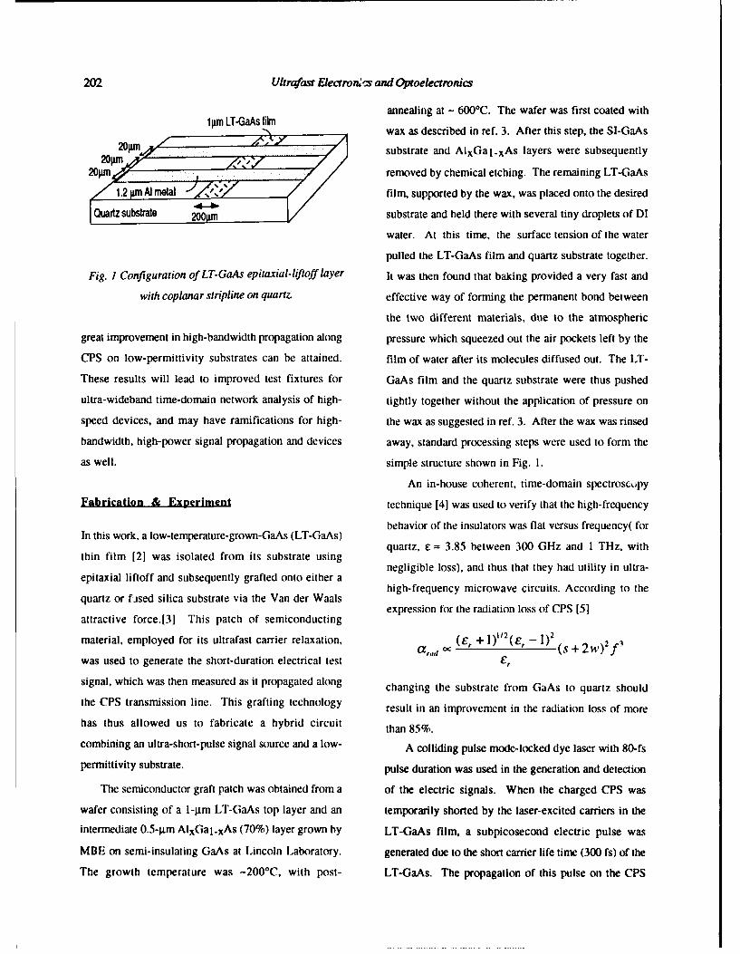
202 Ultrafast Electronics and Oproelectronics
annealing at - 600*C. The wafer was first coated with1 pm LT-Ga~s fiwax as described in ref. 3. After this step, the SI-GaAs
20 , - .'substrate and AlxGal-xAs layers were subsequently
removed by chemical etching. The remaining LT-GaAs
1.2 pAmA metal .' film, supported by the wax, was placed onto the desired
Quartz tate substrate and held there with several tiny droplets of DI
water. At this time, the surface tension of the water
pulled the LT-GaAs film and quartz substrate together.
Fig. I Configuration of LT-GaAs epitaxial-liftoff layer It was then found that baking provided a very fast and
with coplanar stripline on quartz. effective way of forming the permanent bond between
the two different materials, due to the atmospheric
great improvement in high-bandwidth propagation along pressure which squeezed out the air pockets left by the
CPS on low-permittivity substrates can be attained, film of water after its molecules diffused out. The LT-
These results will lead to improved test fixtures for GaAs film and the quartz substrate were thus pushed
ultra-wideband time-domain network analysis of high- tightly together without the application of pressure on
speed devices, and may have ramifications for high- the wax as suggested in ref. 3. After the wax was rinsed
bandwidth, high-power signal propagation and devices away, standard processing steps were used to form the
as well. simple structure shown in Fig. 1.
An in-house coherent, time-domain spectroscopy
Fabrication & Experiment technique [4] was used to verify that the high-frequency
behavior of the insulators was flat versus frequency( forIn this work, a low-temperature-grown-GaAs (LT-GaAs)
thin film [2] was isolated from its substrate using quartz, E- 3.85 between 300 GIz and 1 THz, withnegligible loss), and thus that they had utility in ultra-
epitaxial liftoff and subsequently grafted onto either a
quartz or fised silica substrate via the Van der Waals high-frequency microwave circuits. According to theexpression for the radiation loss of CPS [5]
attractive force.[3] This patch of semiconducting
material, employed for its ultrafast carrier relaxation, (e, + 1)1/ 2 (e, - 1)2OC,.a o•(s+2w) 2f 3
was used to generate the short-duration electrical test Er
signal, which was then measured as it propagated along changing the substrate from GaAs to quartz should
the CPS transmission line. This grafting technology result in an improvement in the radiation loss of more
has thus allowed us to fabricate a hybrid circuit than 85%.
combining an ultra-short-pulse signal source and a low- A colliding pulse mode-locked dye laser with 80-fs
permittivity substrate. pulse duration was used in the generation and detection
The semiconductor graft patch was obtained from a of the electric signals. When the charged CPS was
wafer consisting of a I-gim LT-GaAs top layer and an temporarily shorted by the laser-excited carriers in the
intermediate 0.5-gim AlxGal.xAs (70%) layer grown by LT-GaAs film, a subpicosecond electric pulse was
MBE on semi-insulating GaAs at Lincoln Laboratory. generated due to the short carrier life time (300 fs) of the
The growth temperature was -200*C, with post- LT-GaAs. The propagation of this pulse on the CPS
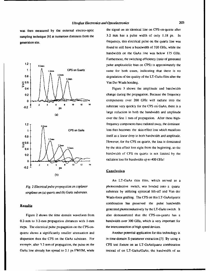
Ultrafast Electronics and Optoelectronics 203
was then measured by the external electro-optic the signal on an identical line on CPS-on-quartz after
sampling technique [61 at numerous distances from the 3.2 mm has a pulse width of only 1.18 ps. In
generation site. frequency, this electrical pulse on the quartz line was
found to still have a bandwidth of 320 GHz, while the
bandwidth on the GaAs line was below 175 GHz.
Furthermore, the switching efficiency (ratio of generated
12 0.2mm pulse amplitude/dc bias on CPS) is approximately the
1 1.2mm CPS on Quartz same for both cases, indicating that there is no
0.8- degradation of the quality of the LT-GaAs film after the
"0.68 Van Der Waals bonding.>0.4 Figure 3 shows the amplitude and bandwidth
0.2 change during the propagation. Because the frequency
0 components over 200 GHz will radiate into the
-0.2 2 4 6 a 10 12 14 substrate very quickly for the CPS on GaAs, there is a
(a) large reduction in both the bandwidth and amplitude
over the first 1 mm of propagation. After these high-1.2 frequency components have radiated away, the dominant
Omil
1 CPS on GaAs loss then becomes the skin effect loss which manifests
0.8 itself as a linear drop in both bandwidth and amplitude.1.2mm
-=0.6 However, for the CPS on quartz, the loss is dominatedo 2.2mm> 0.4- 3.2mm by the skin effect loss right from the beginning, so the
0.2 bandwidth of CPS on quartz is not limited by the
0 radiation loss for bandwidth up to 400 GHz!
2 4 6 8 10 12 14-0.2 -psConclusion
(b)
An LT-GaAs thin film, which served as a
Fig. 2 Electrical pulse propagation on coplanar photoconductive switch, was bonded onto a quartz
striplines on (a) quartz and (b) GaAs substrates. substrate by utilizing epitaxial lift-off and Van der
Waals-force grafting. The CPS on this LT-GaAs/quartz
Results combination has preserved the pulse bandwidth
generated photoconductively by the LT-GaAs switch. It
Figure 2 shows the time domain waveform from also demonstrated that the CPS-on-quartz has a
0.2-mm to 3.2-mm propagation distances with 1-mm bandwidth over 300 GHz, which is very important for
steps. The electrical pulse propagation on the CPS-on- the interconnection of high speed devices.
quartz shows a significantly smaller attenuation and Another potential application for this technology is
dispersion then the CPS on the GaAs substrate. For in time-domain S-parameter extraction.[7J By using a
example, after 3.2 mm of propagation, the pulse on the CPS test fixture on an LT-GaAs/quartz combination
GaAs line already has spread to 2.1 ps FWtlM, while instead of on LT-GaAs/GaAs, the bandwidth of an
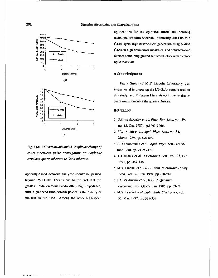
204 Ultrafast Electronics and Optoelectronics
450. applications for the epitaxial liftoff and bonding
400WA technique are ultra-wideband microstrip lines on thin350300 GaAs layers, high-electric-field generation using grafted250 Quartz GaAs on high-breakdown substrates, and optoelectronic
150 so. devices combining grafted semiconductors with electro-100 -a--- GaAsso optic materials.
0 1 2 3
Distance (mm) Acknowledgment(a)
Frank Smith of MIT Lincoln Laboratory was
1 •instrumental in preparing the LT-GaAs sample used in
0. .. this study, and Yongqian Liu assisted in the terahertz-.,ao0.6 beam measurement of the quartz substrate.
0.5
04S0.3
0.2 •GA
0 1. D.Grischkowsky et at., Phys. Rev. Lett., vol. 59,01 2 no. 15, Oct. 1987, pp. 16 63 - 16 6 6 .
Distance (mim)
2. F.W. Smith el al., Appl. Phys. Lett., vol 54,(b)
March 1989, pp. 890-892.3. E. Yablonovitch et al., App!. Phys. Lett, vol 56,
Fig. 3 (a) 3-dB bandwidth and (b) amplitude change ofJune 1990, pp. 2419-2421.
short electrical pulse propagating on coplanar
4. J. Chwalek et al., Electronics Let:., vol. 27, Feb.striplines, quartz substrate vs GaAs substrate.1991, pp. 447-448.
5. M.Y. Frankel et al. IEEE Tran. Microwave Theory
optically-based network analyzer should be pushed Tech., vol. 39, June 1991, pp.9 10-9 16.
beyond 250 GHz. This is due to the fact that the 6. J.A. Valdmanis et al., IEEE J. Quantun
greatest limitation to the bandwidth of high-impedance, Electronic., vol. QE-22, Jan. 1986, pp. 69-78.
ultra-high-speed time-domain probes is the quality of 7. M.Y. Frankel et al, Solid-State Electronics, vol.
the test fixture used. Among the other high-speed 35, Mar. 1992, pp. 325-332.
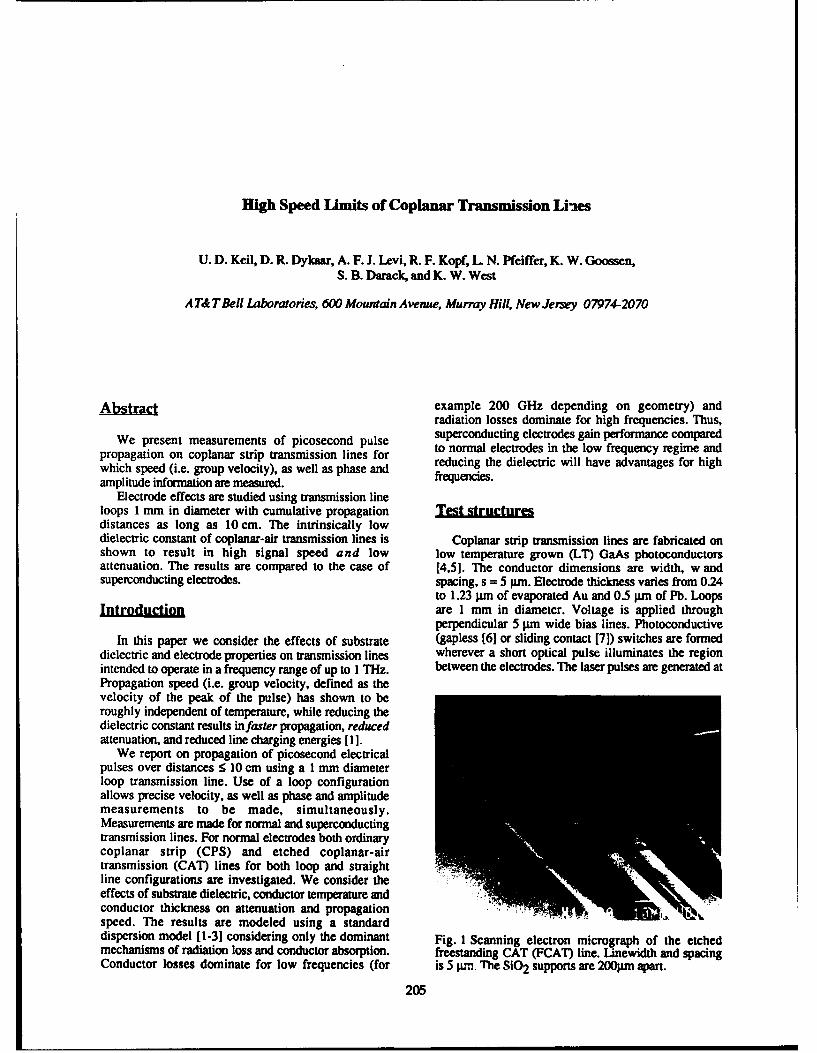
High Speed Limits of Coplanar Transmission Li"es
U. D. Keil, D. R. Dykaar, A. F. J. Levi, R. F. Kopf, L. N. Pfeiffer, K. W. Goossen,S. B. Darack, and K. W. West
A T& T Bell Laboratories, 600 Mountain Avenue, Murray Hill, New Jersey 07974-2070
Abstract example 200 GHz depending on geometry) andradiation losses dominate for high frequencies. Thus,
We present measurements of picosecond pulse superconducting electrodes gain performance comparedpropagation on coplanar strip transmission lines for to normal electrodes in the low frequency regime andwhich speed (i.e. group velocity), as well as phase and reducing the dielectric will have advantages for highamplitude information are measured. frequencies.
Electrode effects are studied using transmission lineloops 1 mm in diameter with cumulative propagation TesLstucturedistances as long as 10 cm. The intrinsically lowdielectric constant of coplanar-air transmission lines is Coplanar strip transmission lines are fabricated onshown to result in high signal speed and low low temperature grown (LT) GaAs photoconductorsattenuation. The results are compared to the case of [4,5]. The conductor dimensions are width, w andsuperconducting electrodes. spacing, s = 5 gim. Electrode thickness varies from 0.24
to 1.23 Wun of evaporated Au and 0.5 pIm of Pb. Loopsu are 1 mm in diameter. Voltage is applied through
perpendicular 5 pim wide bias lines. PhotoconductiveIn this paper we consider the effects of substrate (gapless [6] or sliding contact [7]) switches are formed
dielectric and electrode properties on transmission lines wherever a short optical pulse illuminates the regionintended to operate in a frequency range of up to 1 THz. between the electrodes. The laser pulses are generated atPropagation speed (i.e. group velocity, defined as thevelocity of the peak of the pulse) has shown to beroughly independent of temperature, while reducing thedielectric constant results in faster propagation, reducedattenuation, and reduced line charging energies [ 1].
We report on propagation of picosecond electricalpulses over distances < 10 cm using a 1 mm diameterloop transmission line. Use of a loop configurationallows precise velocity, as well as phase and amplitudemeasurements to be made, simultaneously.Measurements are made for normal and superconductingtransmission lines. For normal electrodes both ordinarycoplanar strip (CPS) and etched coplanar-airtransmission (CAT) lines for both loop and straightline configurations are investigated. We consider theeffects of substrate dielectric, conductor temperature andconductor thickness on attenuation and propagationspeed. The results are modeled using a standarddispersion model [1-31 considering only the dominant Fig. 1 Scanning electron micrograph of the etchedmechanisms of radiation loss and conductor absorption. freestanding CAT (FCAT) line. Linewidth and spacingConductor losses dominate for low frequencies (for is 5 gn. The SiO 2 supports are 200prm apart.
205
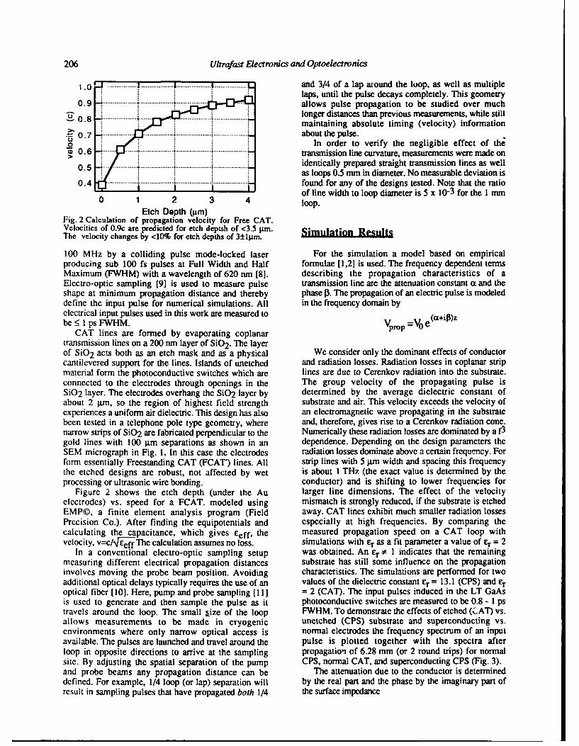
206 Ultrafast Electronics and Optoelectronics
1.0 and 3/4 of a lap around the loop, as well as multiplelaps, until the pulse decays completely. This geometry
0.9 ............. ......... .......... allows pulse propagation to be studied over muchS0longer distances than previous measurements, while stillS0.8 maintaining absolute timing (velocity) information
0.7 about the pulse.o In order to verify the negligible effect of the"> 0.6 transmission line curvature, measurements were made on
0. 5 identically prepared straight transmission lines as wellas loops 0.5 nun in diameter. No measurable deviation is
0.4 .found for any of the designs tested. Note that the ratioof line width to loop diameter is 5 x 10⁻³ for the 1 mm
0 1 2 3 4 loop.Etch Depth (g.m)
Fig. 2 Calculation of propagation velocity for Free CAT.Velocities of 0.9c are predicted for etch deptsh of <3.5 pim. Simulation ResultsThe velocity changes by <10% for etch depths of 3±lptm.
100 MHz by a colliding pulse mode-locked laser For the simulation a model based on empiricalproducing sub 100 fs pulses at Full Width and Half formulae [1,2] is used. The frequency dependent termsMaximum (FWHM) with a wavelength of 620 run [8]. describing the propagation characteristics of aElectro-optic sampling [9] is used to measure pulse transmission line are the attenuation constant a and theshape at minimum propagation distance and thereby phase P3. The propagation of an electric pulse is modeleddefine the input pulse for numerical simulations. All in the frequency domain byelectrical input pulses used in this work are measured to (a+$)zbe•< 1 ps FWHM. V -V e
CAT lines are formed by evaporating coplanar proptransmission lines on a 200 nm layer of SiO 2 . The layerof SiO 2 acts both as an etch mask and as a physical We consider only the dominant effects of conductorcantilevered support for the lines. Islands of unetched and radiation losses. Radiation losses in coplanar stripmaterial form the photoconductive switches which are lines are due to Cerenkov radiation into the substrate.connected to the electrodes through openings in the The group velocity of the propagating pulse isSiO2 layer. The electrodes overhang the SiO2 layer by determined by the average dielectric constant ofabout 2 pm, so the region of highest field strength substrate and air. This velocity exceeds the velocity ofexperiences a uniform air dielectric. This design has also an electromagnetic wave propagating in the substratebeen tested in a telephone pole type geometry, where and, therefore, gives rise to a Cerenkov radiation cone.narrow strips of SiO2 are fabricated perpendicular to the Numerically these radiation losses are dominated by a f3gold lines with 100 Itm separations as shown in an dependence. Depending on the design parameters theSEM micrograph in Fig. 1. In this case the electrodes radiation losses dominate above a certain frequency. Forform essentially Freestanding CAT (FCAT') lines. All strip lines with 5 ;Lm width and spacing this frequencythe etched designs are robust, not affected by wet is about 1 THz (the exact value is determined by theprocessing or ultrasonic wire bonding. conductor) and is shifting to lower frequencies for
Figure 2 shows the etch depth (under the Au larger line dimensions. The effect of the velocityelectrodes) vs. speed for a FCAT. modeled using mismatch is strongly reduced, if the substrate is etchedEMP©, a finite element analysis program (Field away. CAT lines exhibit much smaller radiation lossesPrecision Co.). After finding the equipotentials and especially at high frequencies. By comparing thecalculating the capacitance, which gives Eeff, the measured propagation speed on a CAT loop withvelocity, v=c/4,ffThe calculation assumes no loss. simulations with E as a fit parameter a value of cr = 2
In a conventional electro-optic sampling setup was obtained. An r * I indicates that the remainingmeasuring different electrical propagation distances substrate has still some influence on the propagationinvolves moving the probe beam position. Avoiding characteristics. The simulations are performed for twoadditional optical delays typically requires the use of an values of the dielectric constant E. = 13.1 (CPS) and Eroptical fiber [10]. Here, pump and probe sampling [IlI = 2 (CAT). The input pulses induced in the LT GaAsis used to generate and then sample the pulse as it photoconductive switches are measured to be 0.8 - 1 pstravels around the loop. The small size of the loop FWHM. To demonstrate the effects of etched (,'-AT) vs.allows measurements to be made in cryogenic unetched (CPS) substrate and superconducting vs.environments where only narrow optical access is normal electrodes the frequency spectrum of an inputavailable. The pulses are launched and travel around the pulse is plotted together with the spectra afterloop in opposite directions to arrive at the sampling propagation of 6.28 mm (or 2 round trips) for normalsite. By adjusting the spatial separation of the pump CPS, normal CAT, and superconducting CPS (Fig. 3).and probe beams any propagation distance can be The attenuation due to the conductor is determineddefined. For example, 1/4 loop (or lap) separation will by the real part and the phase by the imaginary part ofresult in sampling pulses that have propagated both 1/4 the surface impedance
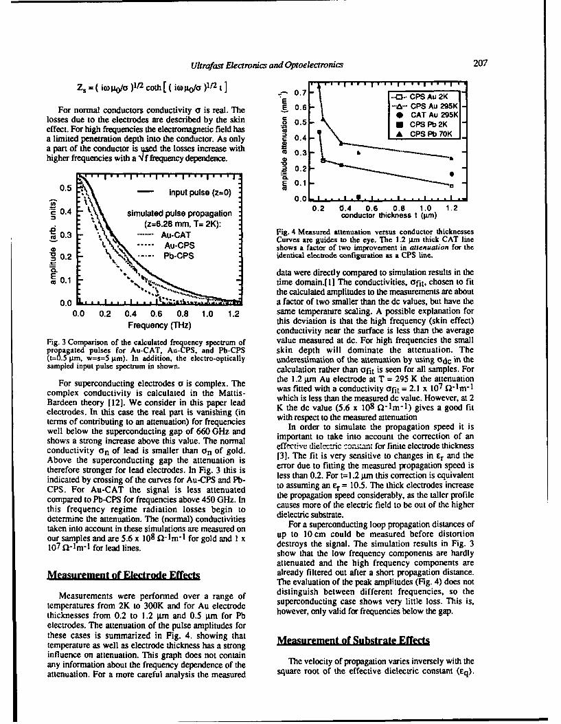
Ultrafast Electronics and Optoelectronics 207
Zs=( i°)Oij/o/)lr2c.J[(io/G)l/2t] ..--- 0.7 I. [1.2S t]
E --0- CPS AU 2KFor normal conductors conductivity a is real. The E 0.6 -.. r. CPS Au 295K1-
losses due to the electrodes are described by the skin _ 0. 5 C I 2,5Keffect. For high frequencies the electromagnetic field has 1=0 - I CPS Pb 2K la limited penetration depth into the conductor. As only C0.4a part of the conductor is ed the losses increase with 0 -'higher frequencies with a f frequency dependence. 0
___________________ ~0.206
0.5 - input pulse (z=0).•
~ ~~~~~~~0.0 .. i..i..,. ...
0 . 0.2 0.4 0.6 0.8 1.0 1.2simulated pulse propagationthickness t (m)
_s0.3 Au-CAT Fig. 4 Measured attenuation versus conductor thicknesses
S.8mT2 Curves are guides to the eye. The 1.2 gtm thick CAT line( shows a factor of two improvement in attenuation for the
0.2 N • .... Pb-CPS identical electrode configuration as a CPS line.S....A-P
E. :. " data were directly compared to simulation results in the'a0.1 .t, , im e domain jt1] The conductivities, of -It, chosen to fit
the calculated amplitudes to the measurements are about0.0 . a factor of two smaller than the dc values, but have the
0.0 0.2 0.4 0.6 0.8 1.0 1.2 same temperature scaling. A possible explanation for
Frequency (THz) this deviation is that the high frequency (skin effect)conductivity near the surface is less than the average
Fig. 3 Comparison of the calculated frequency spectrum of value measured at dc. For high frequencies the smallpropagated pulses for Au-CAT, Au-CPS, and Pb-CPS skin depth will dominate the attenuation. The(t=0.5 pim, w=s=5 gm). In addition, the electro-optically underestimation of the attenuation by using Gdc in thesampled input pulse spectrum in shown. calculation rather than ofit is seen for all samples. For
For superconducting electrodes a is complex. The the 1.2 ;am Au electrode at T = 295 K the attenuationcomplex conductivity is calculated in the Mattis- was fitted with a conductivity ofit = 2.1 x 10⁷ fl-lm-1
Bardeen theory [12]. We consider in this paper lead which is less than the measured dc value. However, at 2electrodes. In this case the real part is vanishing (in K the dc value (5.6 x 10⁸ fl-lm-1) gives a good fitterms of contributing to an attenuation) for frequencies with respect to the measured attenuationwell below the superconducting gap of 660 GHz and In order to simulate the propagation speed it is
shows a strong increase above this value. The normal important to take into account the correction of an
conductivity On of lead is smaller than On of gold. effective dielectric ":ons.t for finite electrode thicknessAbove the superconducting gap the attenuation is [3]. The fit is very sensitive to changes in £r and the
therefore stronger for lead electrodes. In Fig. 3 this is error due to fitting the measured propagation speed isindicated by crossing of the curves for Au-CPS and Pb- less than 0.2. For t=-1.2 pm this correction is equivalentCPS. For Au-CAT the signal is less attenuated to assuming an er= 10.5. The thick electrodes increase
compared to Pb-CPS for frequencies above 450 GHz. In the propagation speed considerably, as the taller profile
this frequency regime radiation losses begin to causes more of the electric field to be out of the higher
determine the attenuation. The (normal) conductivities dielectric substrate.taken into account in these simulations are measured on For a superconducting loop propagation distances of
our samples and are 5.6 x 10⁸ jj-lm-I for gold and I x up to 10 cm could be measured before distortion107 j1-lm- for lead lines, destroys the signal. The simulation results in Fig. 3
show that the low frequency components are hardlyattenuated and the high frequency components are
Measurement of Electrode Effects already filtered out after a short propagation distance.The evaluation of the peak amplitudes (Fig. 4) does not
Measurements were performed over a range of distinguish between different frequencies, so thetemperatures from 2K to 300K and for Au electrode superconducting case shows very little loss. This is,thicknesses from 0.2 to 1.2 Kin and 0.5 gim for Po however, only valid for frequencies below the gap.electrodes. The attenuation of the pulse amplitudes forthese cases is summarized in Fig. 4. showing that Measurement of Substrate Effectstemperature as well as electrode thickness has a stronginfluence on attenuation. This graph does not containany information about the frequency dependence of the The velocity of propagation varies inversely with theattenuation. For a more careful analysis the measured square root of the effective dielectric constant (Eq).
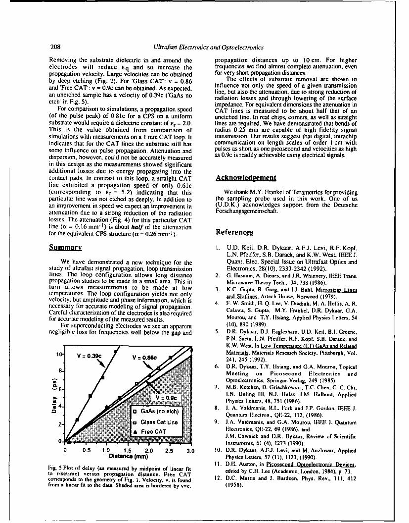
208 Ulrrafasit Electronics and Optoelectroniacs
Removing the substrate dielectric in and around the propagation distances up to 10 cm. For higherelectrodes will reduce Eq and so increase the frequencies we find almost complete attenuation, evenpropagation velocity. Large velocities can be obtained for very short propagation distances.by deep etching (Fig. 2). For 'Glass CAT': v = 0.86 The effects of substrate removal are shown toand 'Free CAT': v = 0.9c can be obtained. As expected, influence not only the speed of a given transmission
line, but also the attenuation, due to strong reduction ofan unetched sample has a velocity of 0.39c ('GaAs no radiation losses and through lowering of the surfaceetch' in Fig. 5). impedance. For equivalent dimensions the attenuation in
For comparison to simulations, a propagation speed CAT lines is measured to be about half that of an(of the pulse peak) of 0.81c for a CPS on a uniform unetched line. In real chips, comers, as well as straightsubstrate would require a dielectric constant of Er = 2.0. lines are required. We have demonstrated that bends ofThis is the value obtained from comparison of radius 0.25 mm are capable of high fidelity signalsimulations with measurements on a I mnu CAT loop. It transmission. Our results suggest that digital, intrachipindicates that for the CAT lines the substrate still has communication on length scales of order 1 cm withsome influence on pulse propagation. Attenuation and pulses as short as one picosecond and velocities as highdispersion, however, could not be accurately measured as 0.9c is readily achievable using electrical signals.in this design as the measurements showed significantadditional losses due to energy propagating into thecontact pads. In contrast to this loop, a straight CAT Acknowledgementline exhibited a propagation speed of only 0.61c(corresponding to Er = 5.2) indicating that this We thank M.Y. Frankel of Terametrics for providingparticular line was not etched as deeply. In addition to the sampling probe used in this work. One of usan improvement in speed we expect an improvement in (U.D.K.) acknowledges support from the Deutscheattenuation due to a strong reduction of the radiation Forschungsgemeinschaft.losses. The attenuation (Fig. 4) for this particular CATline (ox = 0.16 mm- 1) is about half of the attenuationfor the equivalent CPS structure (ca = 0.26 mm- 1). References
a 1. U.D. Keil, D.R. Dykaar, A.FJ. Levi, R.F. Kopf,L.N. Pfeiffer, S.B. Darack, and K.W. West, IEEE J.
We have demonstrated a new technique for the Quant. Elec. Special Issue on Ultrafast Optics andstudy of ultrafast signal propagation, loop transmission Electronics, 28(10), 2333-2342 (1992).lines. The loop configuration allows long distance 2. G. Ilasnain, A. Dienes, and J.R. WhinneTy, I-•TEE Trans.propagation studies to be made in a small area. This in Microwave Theory Tech.. 34, 738 (1986).turn allows measurements to be made at low 3. K.C. Gupta, R. Garg, and IU. Bahl, Micsrip.. Linestemperatures. The loop configuration yields not only and Slotlinc, Artech Hlouse. Norwood (1979).velocity, but amplitude and phase information, which is 4. F. W. Smith, II. Q. L.ee, V. Diadiuk, M. A. IHollis, A. R.necessary for accurate modeling of signal propagation. Calawa, S. Gupta. M.Y. Frankel. D.R. Dykaar. GA.Careful characterization of the electrodes is also required Mourou, and T.Y. l.siang. Applied Physics Letters, 54for accurate modeling of the measured results.
For superconducting electrodes we see an apparent (10), 890 (1989).negligible loss for frequencies well below the gap and 5. D.R. Dykaar, DJ. Eaglesham, U.D. Keil, B.I. Greene,
P.N. Sacta, L.N. Pfeiffer, R.F. Kopf, S.B. Darack, andK.W. West, In Low Temperature (L.T) GaAs and Related
1 Materials, Materials Research Society, Pittsburgh, Vol.V 0.39c V= 0.86c 6 241, 245 (1992).6. D.R. Dykaar. T.Y. 1lsiang. and G.A. Mourou. Topical
8. .Meeting on Picosecond Electronics andOptoelectronics, Springer-Verlag, 249 (1985).
7. M.B. Ketchen, D. Grischkowski, T.C. Chen, C.-C. Chi,I.N. Duling Ill. N.J. lialas, I.M. lialbout, Applied
x2 - - Physics Letters, 48, 751 (1986)."o4 8. J. A. Valdmanis, R.L. Fork and J.P. Gordon, IFEE J.
S. .! GaAs (no etch) Quantum Electron., QE-22, 112, (1986).a Glass Cat bne 9. JA. Valdmanis, and G.A. Mourou, i1EE-E J. Quantum
Electronics, QIF-22, 69 (1986). andJ.M. Chwalek and D.R. Dykaar. Review of Scientific
I' : •. IInstruments, 61 (4). 1273 (1990).0 0.5 1.0 1.5 2.0 2.5 3.0 10. D.R. Dykaar, A.FJ. Levi, and M. Anflowar, Applied
Distance (mm) Physics Letters, 57 (11), 1123, (1990).11. D.II. Auston, in Picosecond Optoclectronic Devices,Fig. 5 Plot of delay (as measured by midpoint of linear fit edited by C.11. Lee (Academic. London, 1984). p. 73.
to risetime) versus propagation distance. Free CAT die byC.Mt a J. (ademi, London, 19). 412corresponds to the geometry of Fig. 1. Velocity. v. is found 12. D.C. Matis and i. Bardeen, Phys. Rev., 111, 412from a linear fit to the data. Shaded area is bordered by v=c. (1958).
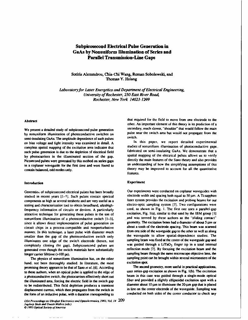
Subpicosecond Electrical Pulse Generation inGaAs by Nonuniform Illumination of Series and
Parallel Transmission-Line Gaps
Sotiris Alexandrou, Chia-Chi Wang, Roman Sobolewski, andThomas Y. Hsiang
Laboratory for Laser Energetics and Department of Electrical Engineering,University of Rochester, 250 East River Road,
Rochester, New York 14623-1299
Abstract that required for the field to move from one electrode to the
other. An important element of this theory is its prediction of a
We present a detailed study of subpicosecond pulse generation secondary, much slower, "shoulder" that would follow the main
by nonuniform illumination of photoconductive switches on pulse near the switch area but would not propagate from the
semi-insulating GaAs. The amplitude dependence of such pulses switch.
on bias voltage and light intensity was examined in detail. A In this paper, we report detailed experimental
complete spatial mapping of the excitation area indicates that studies of nonuniform illumination of photoconductive gaps.such pulse generation is due to the depletion of electrical field fabricated on semi-insulating GaAs. We demonstrate that aby photocarriers in the illuminated section of the gap. spatial mapping of the electrical pulses allows us to verifyPicosecond pulses were generated by this method on series gaps directly the main features of the Sano theory and also providesin a coplanar waveguide for the first time and were found to an understanding of how the simplifying assumptions of thiscontain balanced, odd modes only. theory may be improved to account for all the quantitative
features.
Introduction Experiment
Generatio,; of subpicosecond electrical pulses has been broadly Our experiments were conducted on coplanar waveguides withstudied in recent years [1-51. Such pulses contain spectral electrode width and spacing both equal to 50lim. A Ti:sapphirecomponents as high as several terahertz and are very useful as a laser system provides the excitation and probing beams for ourtesting and characterization tool to obtain broadband, ultrahigh- electro-optic sampling system [71. Two configurations werefrequency information of circuits or devices. A particularly used, as shown in Fig. I. The first one uses a parallel-gapattractive technique for generating these pulses is the use of excitation, Fig. 1(a), similar to that used by the IBM group Il]nonuniform illumination of a photoconductive switch 11-3]. and was iermed by these authors as the "sliding contact"since it allows direct implementation of pulse generation on geometry. The excitation beam had a diameter of about 5 pm orcircuit chips in a process-compatible and nonperturbative about a tenth of the electrode spacing. This beam was scannedmanner. In this technique, a laser pulse with diameter much from one side of the waveguide gap to the other as well as alongsmaller than the gap of the photoconductive switch only the waveguide to allow spatial-dependence studies. Theilluminates one edge of the switch electrode (hence, not sampling beam was fixed at the center of the waveguide gap andcompletely closing the gap). Subpicosecond pulses are was guided through a LiTaO3 finger tip in a total internalgenerated even though the switch materials have substantially reflection mode (71. By focusing the excitation beam and thelonger carrier lifetime (>100 ps). sampling beam through the same microscope objective lens, the
The physics of nonuniform illumination has, on the other sampling point can be brought within several micrometers of thehand, not been thoroughly studied. In literature, the most excitation spot.promising theory appears to be that of Sano et al. (6]. According The second geometry, more useful in practical applications,to these authors, when an optical pulse is applied to the edge of uses series-gap excitation as shown in Fig. i(b). The excitationa photoconductive switch, the photocarriers effectively short out beam in this case was guided through a single-mode opticalthe illuminated area, forcing the electric field in the switch gap fiber and provided a slightly ellipsoidal excitation spot with ato be redistributed. This field depletion produces a transient diameter about 10 pm to illuminate the 20-pm gap that is placeddisplacement current, which then propagates from the switch in in line on the center electrode of the waveguide. Sampling wasthe form of an inductive pulse, with a duration corresponding to conducted on both sides of the center conductor to check any
OSA Proceedings on Ubrafast Electronics and Oproelecironicx 1993. VoL 14 209Jagdeep Shah and Uniesh Mishra (eds.)0 1993 Opticat Sockety f/America
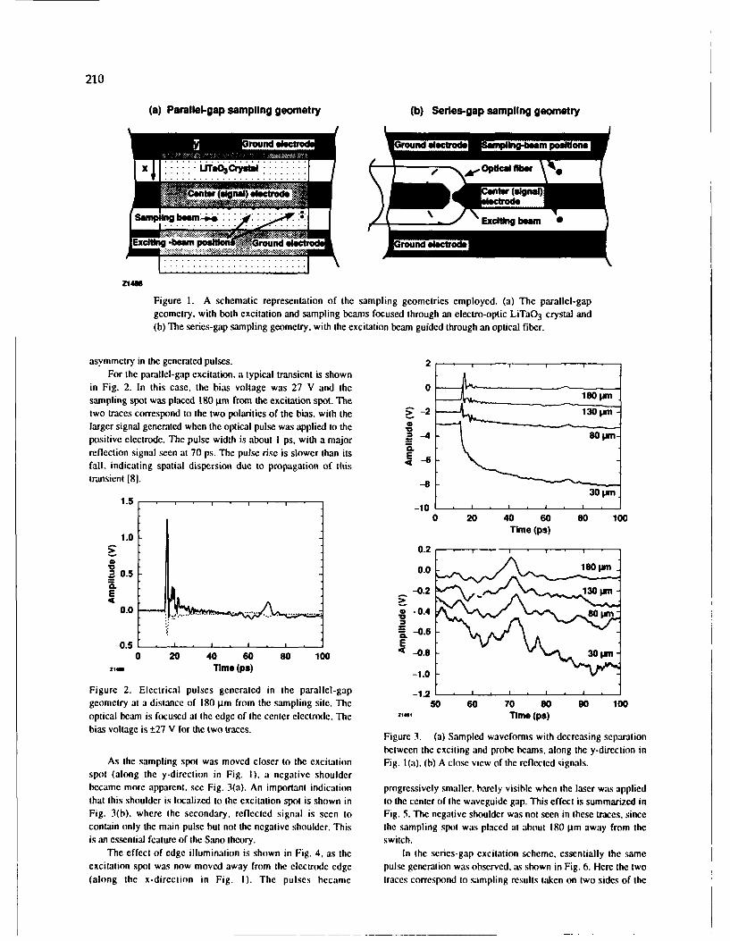
210
(a) Parallel-gap sampling geometry (b) Series-gap sampling geometry
rouound C lecrod *1 wipng-besam poeltiona'
t ..~ .... ...2 2 1. ..... . .
ter signl) lectode er signal)
f Exciting beam
Ex~~g-beam poelil w roun A unwd electode
Figure 1. A schematic representation of the sampling geometries employed. (a) The parallel-gapgeometry, with both excitation and sampling beams focused through an electro-optic LiTaO 3 crystal and(b) The series-gap sampling geometry, with the excitation beam guided through an optical fiber.
asymmetry in the generated pulses. 2For the parallel-gap excitation, a typical transient is shown
in Fig. 2. In this case, the bias voltage was 27 V and the 0-------sampling spot was placed 180 gtm from the excitation spot. Thetwo traces correspond to the two polarities of the bias, with the > -2------•-13
larger signal generated when the optical pulse was applied to thepositive electrode. The pulse width is about I ps. with a major -4 80 Pm-
reflection signal seen at 70 ps. The pulse rise is slower than its Efall, indicating spatial dispersion due to propagation of this -6
transient 181. - -
30 pm1.5 -10
0 20 40 60 80 100Time (ps)
1.0
S0.5 0.0
0.0 8-0P.40.5L 130 Is -o.
E~ -0.2
-0.6-0.5 IE
0 20 40 60 80 100z14M Time (ps) -1.0
Figure 2. Electrical pulses generated in the parallel-gap -1.2_. _____,_______•geometry at a distance of 180 pm from the sampling site. The 50 60 70 80 90 100optical beam is focused at the edge of the center electrode. The ZT41 lime (ps)bias voltage is ±27 V for the two traces. Figure 3. (a) Sampled waveforms with decreasing separation
between the exciting and probe beams, along the y-direction inAs the sampling spot was moved closer to the excitation Fig. I(a). (b) A close view of the reflected signals.
spot (along the y-direction in Fig. I). a negative shoulderbecame more apparent, see Fig. 3(a). An important indication progressively smaller, barely visible when the laser was appliedthat this shoulder is localized to the excitation spot is shown in to the center of the waveguide gap. This effect is summarized inFig. 3(b). where the secondary, reflected signal is seen to Fig. 5. The negative shoulder was not seen in these traces, sincecontain only the main pulse but not the negative shoulder. This the sampling spot was placed at about I80 pim away from theis an essential feature of the Sano theory. switch.
The effect of edge illumination is shown in Fig. 4, as the In the series-gap excitation scheme, essentially the sameexcitation spot was now moved away from the electrode edge pulse generation was observed, as shown in Fig. 6. Here the two(along the x-dircction in Fig. I). The pulses became traces correspond to sampling results taken on two sides of the
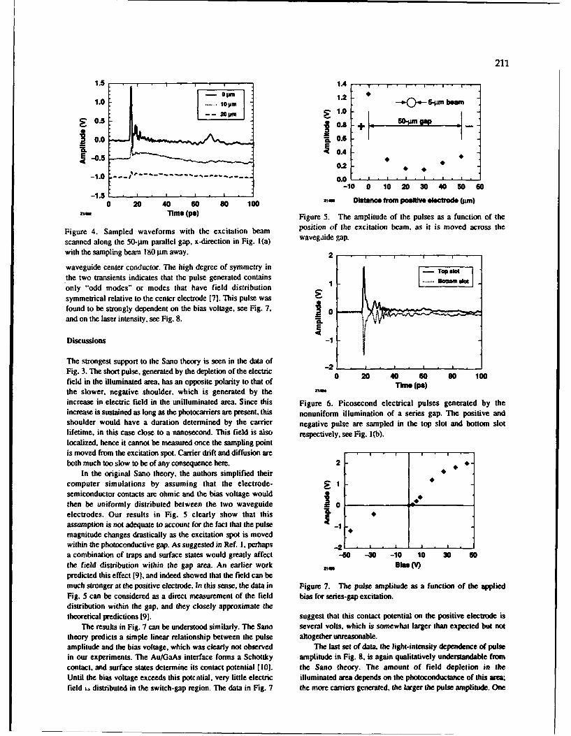
211
1.5 -- •1.4 . , . , . , . , . , . , .1.2
1.0 1.2o- - 5011 bea1
S0.5 7 50L -pmO0.68
0.0 ,,0.6
L •0.4-0.5 ----
0.2 * *-1.0 -.-.. .. 0.0
-10 0 10 20 30 40 50 60
0 20 40 60 80 100 Zm D ii p@Sltroe(1i)Z4 Time (pa) Figure 5. The amplitude of the pulses as a function of the
Figure 4. Sampled waveforms with the excitation beam position of the excitation beam, as it is moved across the
scanned along the 50-pm parallel gap, x-direction in Fig. 1(a) wavegjide gap.
with the sampling beam 180 pm away.
waveguide center conductor. The high degree of symmetry in
the two transients indicates that the pulse generated contains
only "odd modes" or modes that have field distribution
symmetrical relative to the center electrode [7]. This pulse was
found to be strongly dependent on the bias voltage, see Fig. 7, 0and on the laser intensity, see Fig. 8. ".
Discussions
The strongest support to the Sano theory is seen in the data ofFig. 3. The short pulse, generated by the depletion of the electric 0 20 40 60 s0 100
field in the illuminated area, has an opposite polarity to that of Time (pa)
the slower, negative shoulder, which is generated by the Zia"
increase in electric field in the unilluminated area. Since this Figure 6. Picosecond electrical pulses generated by theincrease is sustained as long as the photocarriers are present, this nonuniform illumination of a series gap. The positive andshoulder would have a duration determined by the carrier negative pulse are sampled in the top slot and bottom slotlifetime, in this case close to a nanosecond. This field is also respectively, see Fig. 1(b).localized, hence it cannot be measured once the sampling pointis moved from the excitation spot. Carrier drift and diffusion are ,both much too slow to be of any consequence here. 2-
In the original Sano theory, the authors simplified their
computer simulations by assuming that the electrode- 1 Isemiconductor contacts are ohmic and the bias voltage would Ithen be uniformly distributed between the two waveguide 0electrodes. Our results in Fig. 5 clearly show that thisassumption is not adequate to account for the fact that the pulse -1magnitude changes drastically as the excitation spot is movedwithin the photoconductive gap. As suggested in Ref. 1, perhaps -- . 'a combination of traps and surface states would greatly affect -60 -30 -10 10 30 sothe field distribution within the gap area. An earlier work 2M sBm (V)predicted this effect 191, and indeed showed that the field can bemuch stronger at the positive electrode. In this sense, the data in Figure 7. The pulse amplitude as a function of the appliedFig. 5 can be considered as a direct measurement of the field bias for series-gap excitation.
distribution within the gap, and they closely approximate the
theoretical predictions [91. suggest that this contact potential on the positive electrode isThe results in Fig. 7 can be understood similarly. The Sano several volts, which is somewhat larger than expected but not
theory predicts a simple linear relationship between the pulse altogether unreasonable.amplitude and the bias voltage, which was clearly not observed The last set of data, the light-intensity dependence of pulsein our experiments. The Au/GaAs interface forms a Schottky amplitude in Fig. 8, is again qualitatively understandable from
contact, and surface states determine its contact potential [101. the Sano theory. The amount of field depletion in theUntil the bias voltage exceeds this potcntial, very little electric illuminated area depends on the photoconductance of this area;field is distributed in the switch-gap region. The data in Fig. 7 the more carriers generated, the larger the pulse amplitude. One
212
10 2. N. Katzenellenbogen and D. Grischkowsky, "Efficient
generation of 380 fs pulses of THz radiation by ultrafast* laser pulse excitation of a biased metal-semiconductor
• I interface," Appl. Phys. Lett. 8, 222-224 (1991).
3. U.D. Keil and D.R. Dykaar"Electro-opcsamplingandI •carrier dynamics at zero propagation distance," Appl.
0.1 Phys. Lett. fIL 1504-1506 (1992).4. S. Alexandrou, C.-C. Wang, T. Y. Hsiang, M. Y. Liu, and
S. Y. Chou, "A 75-GHz silicon metal-semiconductor-metal0.01. ........ . Schottky photodiode," submitted to Appl. Phys. Lett.
0.01 0.1 1 10 (November, 199.2).z• Ught Intemnsty(mW) 5. S. Y. Chou, Y. Liu, W. Khalil, T. Y. Hsiang, and
S. Alexandrou, "Ultrafast nanoscale metal-semiconductor-Figure 8. The pulse amplitude as a function of the incident metal photodetectors on bulk and low-temperature grownlight intensity for series-gap excitation. GaAs." Appi. Phys. Lett. 61, 819-821 (1992).
6. E. Sano and T. Shibata, "'Mechanism of subpicosecondexpects that at a high enough light intensity, the field would be e al pus generatio bycasmmetric econ"
completely depleted and the pulse height would saturate to a ap p uyse gett i by 2748-2750(1989).plateau. This appears not to have been attained in our Appl. Phys. Let oe 5, 2748-2750 (1989).experiments. 7. S. Alexandrou, R. Sobolewski, and T. Y. Hsiang, "rTime-
domain characterization of bent coplanar waveguides,"
Acknowledgments IEEE J. Quantum Electron. 28, 2325-2332 (1992).8. T. Y. lHsiang. 3. F. Whitaker, R. Sobolewski, D. R. Dykaar,
The authors would like to thank D. R. Dykaar and Y. Kostoulas an GY.a. Mourou , Rop on characteRistics of
for their help. This work was supported in part by the University p nd elActrica tran ion canaristips.o
Research Initiative at the University of Rochester sponsored by picosecond electrical transients on coplanar striplines,"the Army Research Office grant No. DAAL03-92-G-01 12. Apl hs.Lt. 51, 1551-1!553 (1987).
9. M. A. Lampert. "'Simplified theory of space-charge-limited
References currents in an insulator with traps," Phys. Rev. 1.3, 1648-
1. D. KrOkel, D. Grischkowsky. and M. B. Ketchen, 1656(1956)."Subpicosecond electrical pulse generation using 10. S.M. Sze, "Metal-semiconductor contacts," Physics orphotoconductive switches with long carrier lifetimes," Semiconductor Devices, 2nd ed. (Wiley, New York,
Appl. Phys. LetL. M, 1046-1047 (1989). 1981). Chap. 5. pp. 245-311.
Ultrafast Probes of Materials/Devices/Circuits
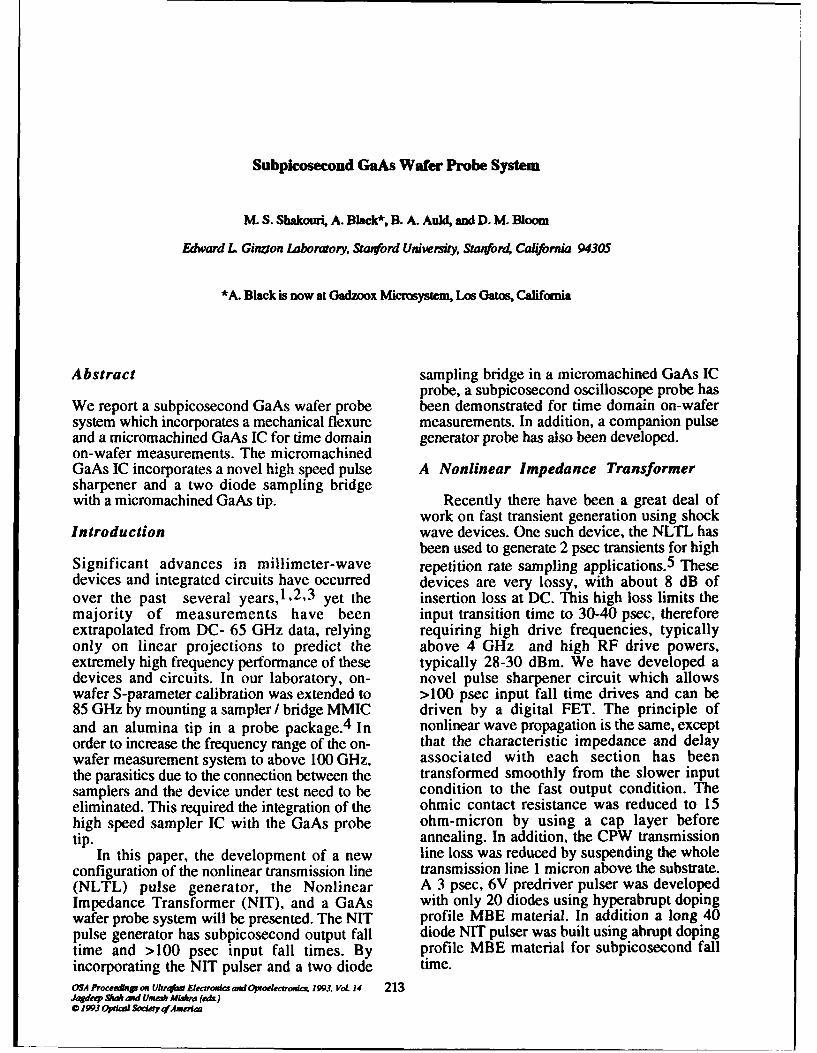
Subplcosecond GaAs Wafer Probe System
M. S. Shakouri, A. Black*, B. A. Auld, and D. M. Bloom
Efward L Ginzton Laboratory, S&alyord University, Stanfor4 California 94305
*A. Black is now at Gadzoox Microsystem, Los Gatos, California
Abstract sampling bridge in a micromachined GaAs ICprobe, a subpicosecond oscilloscope probe has
We report a subpicosecond GaAs wafer probe been demonstrated for time domain on-wafersystem which incorporates a mechanical flexure measurements. In addition, a companion pulseand a micromachined GaAs IC for time domain generator probe has also been developed.on-wafer measurements. The micromachinedGaAs IC incorporates a novel high speed pulse A Nonlinear Impedance Transformersharpener and a two diode sampling bridgewith a micromachined GaAs tip. Recently there have been a great deal of
work on fast transient generation using shockIntroduction wave devices. One such device, the NLTL has
been used to generate 2 psec transients for highSignificant advances in millimeter-wave repetition rate sampling applications. 5 Thesedevices and integrated circuits have occurred devices are very lossy, with about 8 dB ofover the past several years, 1 ,2,3 yet the insertion loss at DC. This high loss limits themajority of measurements have been input transition time to 30-40 psec, thereforeextrapolated from DC- 65 GHz data, relying requiring high drive frequencies, typicallyonly on linear projections to predict the above 4 GHz and high RF drive powers,extremely high frequency performance of these typically 28-30 dBm. We have developed adevices and circuits. In our laboratory, on- novel pulse sharpener circuit which allowswafer S-parameter calibration was extended to >100 psec input fall time drives and can be85 GHz by mounting a sampler / bridge MMIC driven by a digital FET. The principle ofand an alumina tip in a probe package. 4 In nonlinear wave propagation is the same, exceptorder to increase the frequency range of the on- that the characteristic impedance and delaywafer measurement system to above 100 GHz, associated with each section has beenthe parasitics due to the connection between the transformed smoothly from the slower inputsamplers and the device under test need to be condition to the fast output condition. Theeliminated. This required the integration of the ohmic contact resistance was reduced to 15high speed sampler IC with the GaAs probe ohm-micron by using a cap layer beforetip. annealing. In addition, the CPW transmission
In this paper, the development of a new line loss was reduced by suspending the wholeconfiguration of the nonlinear transmission line transmission line 1 micron above the substrate.(NLTL) pulse generator, the Nonlinear A 3 psec, 6V predriver pulser was developedImpedance Transformer (NIT), and a GaAs with only 20 diodes using hyperabrupt dopingwafer probe system will be presented. The NIT profile MBE material. In addition a long 40pulse generator has subpicosecond output fall diode NIT pulser was built using abrupt dopingtime and >100 psec input fall times. By profile MBE material for subpicosecond fallincorporating the NIT pulser and a two diode time.OSA hocee,,x,,,,, UIkr• Elk oim ,Opoemonmim 1993. Vot 14 213Jagdae A? ,amd Una*m M/m,-a (e&)* 1993 01pdwi ?ly zfAmuela
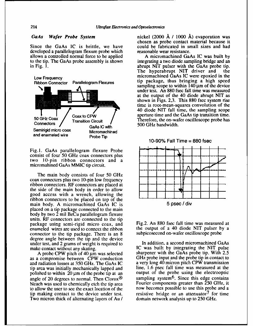
214 U/trafast Eectronics and Optoe/ectronics
GaAs Wafer Probe System nickel (2000 A / 1000 A) evaporation waschosen as probe contact material because it
Since the GaAs IC is brittle, we have could be fabricated in small sizes and haddeveloped a parallelogram flexure probe which reasonable wear resistance.allows a controlled normal force to be applied A micromachined GaAs IC was built byto the tip. The GaAs probe assembly is shown integrating a two diode sampling bridge and anin Fig. 1. abrupt NIT pulser with the GaAs probe tip.
The hyperabrupt NIT driver and theLow Frequency micromachined GaAs IC were epoxied in theRibbon Connector Parallelogram Flexures tip package, thus bringing a high speed
sampling scope to within 140 gm of the deviceunder test. An 880 fsec fall time was measuredat the output of the 40 diode abrupt NIT asshown in Figs. 2,3. This 880 fsec system risetime is root-mean-squares convolution of the40 diode NIT fall time, the sampling scopeaperture time and the GaAs tip transition time.
Connec rs Transition Circuit Therefore, the on-wafer oscilloscope probe hasEGaAs IC with 500 GHz bandwidth.
Semirigid micro coax Micromachinedand enameled wire Probe Tip
10-90% Fall Time = 880 fsec
Fig. 1. GaAs parallelogram flexure Probeconsist of four 50 GHz coax connectors plustwo 10-pin ribbon connectors and amicromahined GaAs MMIC tip circuit.
The main body consists of four 50 GHz O r I Icoax connectors plus two 10-pin low frequencyribbon connectors. RF connectors are placed at -
the side of the main body in order to allowgood access with a wrench, allowing theribbon connectors to be placed on top of themain body. A micromachined GaAs IC is 5 psec /divplaced on a tip package connected to the mainbody by two 2 mil BeCu parallelogram flexureunits. RF connectors are connected to the tippackage using semi-rigid micro coax, and Fig.2. An 880 fsec fall time was measured atenameled wires are used to connect the ribbon the output of a 40 diode NIT pulser by aconnector to the tip package. There is an 8 subpicosecond on-wafer oscilloscope probedegree angle between the tip and the deviceunder test, and 2 grams of weight is required to In addition, a second micromachined GaAsmake contact without any skating. IC was built by integrating the NIT pulse
A probe CPW pitch of 40 pgm was selected sharpener with the GaAs probe tip. With 2.5as a compromise between CPW conduction GHz probe input and the probe tip in contact toand radiation losses at 350 GHz. The GaAs IC a very long 40 micron pitch CPW transmissiontip area was initially mechanically lapped and line, 1.6 psec fall time was measured at thepolished to within 20 pgm of the probe tip at an output of the probe using the electroopticangle of 20 degrees to normal. Then Clorox® sampling system6 . Since this edge containsbleach was used to chemically etch the tip area Fourier components greater than 250 GHz, itto allow the user to see the exact location of the now becomes possible to use this probe and atip making contact to the device under test. resistive bridge or an attenuator 7 for timeTwo micron thick of alternating layers of Au I domain network analysis up to 250 GHz.
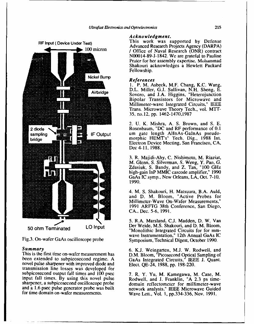
Ultrafast Electronics and Optoelectronics 215
Acknowledgment.RF Input (Device Under Test) This work was supported by Defense
Advanced Research Projects Agency (DARPA)S 100 micron / Office of Naval Research (ONR) contract
N00014-89-J-1842. We are grateful to PaulinePrater for her assembly expertise. MohammadShakouri acknowledges a Hewlett PackardFellowship.
Nickel Bump References1. P. M. Asbeck, M.F. Chang, K.C. Wang,D.L. Miller, G.J. Sullivan, N.H. Sheng, E.
Airbridge Sovero, and J.A. Higgins, "HeterojunctionBipolar Transistors for Microwave andMillimeter-wave Integrated Circuits," IEEETrans. Microwave Theory Tech., vol. MTT-35, no.12, pp. 1462-1470,1987
2. U. K. Mishra, A. S. Brown, and S. E.2 diode •,Rosenbaum, "DC and RF performance of 0.1sampling IF Output um gate length AllnAs-GalnAs pseudo-bridge ! morphic HEMT's" Tech. Dig., 1988 Int.
Electron Device Meeting, San Francisco, CA,Dec 4-11, 1988.
3. R. Majidi-Ahy, C. Nishimoto, M. Riaziat,M. Glenn, S. Silverman, S. Weng, Y. Pao, G.Zdasiuk, S. Bandy, and Z. Tan, "100 GHzhigh-gain InP MMIC cascode amplifier," 1990GaAs IC symp., New Orleans, LA, Oct. 7-10,1990.
4. M. S. Shakouri, H. Matsuura, B.A. Auld,and D. M. Bloom, "Active Probes forMillimeter-Wave On-Wafer Measurements,"1991 ARFTG 38th Conference, San Diego,CA., Dec. 5-6, 1991.
5. R.A. Marsland, C.J. Madden, D. W. Van50 ohm Terminated LO Input Der Weide, M.S. Shakouri, and D. M. Bloom,
"Monolithic Integrated Circuits for for mm-wave Instrumentation," 12th Annual GaAs IC
Fig.3. On-wafer GaAs oscilloscope probe Symposium, Technical Digest, October 1990.
Summary 6. K.J. Weingarten, M.J. W. Rodwell, andThis is the first time on-wafer measurement has D.M. Bloom, "Picosecond Optical Sampling ofbeen extended to subpicosecond regime. A GaAs Integrated Circuits," IEEE J. Quant.novel pulse sharpener with improved diode and Elect. QE-24, 1988, pp. 198-220.transmission line losses was developed forsubpicosecond output fall times and 100 psec 7. R. Y. Yu, M. Kamegawa, M. Case, M.input fall times. By using this novel pulse Rodwell, and J. Franklin, "A 2.3 ps time-sharpener, a subpicosecond oscilloscope probe domain reflectometer for millimeter-waveand a 1.6 psec pulse generator probe was built network analysis," IEEE Microwave Guidedfor time domain on-wafer measurements. Wave Lett., Vol. 1, pp.334-336, Nov. 1991.
Highly Reproducible Optoelectronic Wafer Probes withFiber Input
M. D. Feuer, S. C. Shunk, and M. C. NussA T& T Bell La bs, 101 Crawfords Corner Roa4 Holmdel New Jersey 07733-3030
P. R. Smith and H. H. LawAT&T Bell Labs, 600 Mountain Avenue, Murray Hill, New Jersey 07974-0636
C. A. BurrusAT& TBell Labs, 791 Holmdel-Keyport Road Holmd4 New Jersey 07733-0400
Abstract We have made calibrated reflection measurementsof a variety of passive devices, and have demonstrated
We have constructed optoelectronic wafer probes with the importance of mode conversion in coplanarfiber pigtails and demonstrated accurate, reproducible waveguide (CPW) structures. Accurate results can bemeasurements of the complex reflection coefficient S II ensured by the addition of ground-bridging straps to theat frequencies up to 125 GHz. Vector accuracy basic CPW probe.enhancement routines, based on the measurement ofknown standard devices, are used to remove the effects Methodof tip reflections and other systematic errors. Ground-bridging straps are shown to suppress the mode Probe tip design and fabrication have been presented inconversion errors which result from asymmetric detail in [2]. In brief, gold CPW transmission linesexcitation of the coplanar waveguide probe. were defined lithographically on a commercial silicon-
on-sapphire substrate, with photoconductive gaps ofimplant-damaged Si located symmetrically on the signal
Introduction line, approximately 1 mm from the contact points. Thecontact bumps were formed by plating 35 pnm of nickel
Optoelectronic testing driven by ultrafast laser pulses with a 4 pm gold overlayer. For some measurements,offers a broad-bandwidth alternative to conventional, ground-bridging straps were added to the basic probespurely electronic S-parameter measurements. Movable to suppress the antisymmetric mode. The straps werewafer probes, which can be used on any device wafer sections of gold-mesh tape, typically 100 pmn wide,suitable for microwave probing, have demonstrated attached with conductive epoxy. Figure 1 shows thebandwidth of 200 GHz [1,21. These optoelectronic layout of a probe tip with ground straps.probes use photoconductive switches to define the To bring the optical signals to the stimulus andstimulus pulses and sampling intervals, with sampling gaps, single-mode fibers with cleaved endstransmission lines anda metal contact bumps at the tips were bonded to the back of the sapphire substrate..o bring the sigunal to and from the device pads. To Since the fibers were not lensed, optical coupling to theachieve accuracy in the Fourier-transformed, frequency- photoconductive gaps was not optimally efficient, butdomain data, one must remove systematic errors, by ample power was available from the mode-locked Ti-applying vector calibration techniques based on probing sapphire laser source, and the gap separation of 80 pmnknown standard devices [2]. However, microscopic provided reasonably low crosstalk.flexing of the tips under the stress of wafer probing can The Ar-pumped, mode-locked Ti-sapphire laserdisturb the alignment of the photoconductive gaps to the was tuned to 760 nm, and the power launched into theinput optical beams, leading to irreproducible errors fibers was limited to 10 mW per fiber. A variablewhich cannot be calibrated out. In the present work, we optical delay was introduced before fiber launch tohave bonded optical fibers to the probe tips to achieve sweep the relative delay of the sampling pulses, and thegreatly improved reproducibility and calibration stimulus beam was mechanically chopped to enableaccuracy in the S-parameter measurements. lock-in detection of the signal. This eliminates signal
OSA P ,oaaOmpu UbrVM £U aidOpoecf•.ic, 1993, VoL 14 216Jqdem p a.nAtd Uuak MId~r (AIL)0 1993 Optica Soda fyqAuwlaz
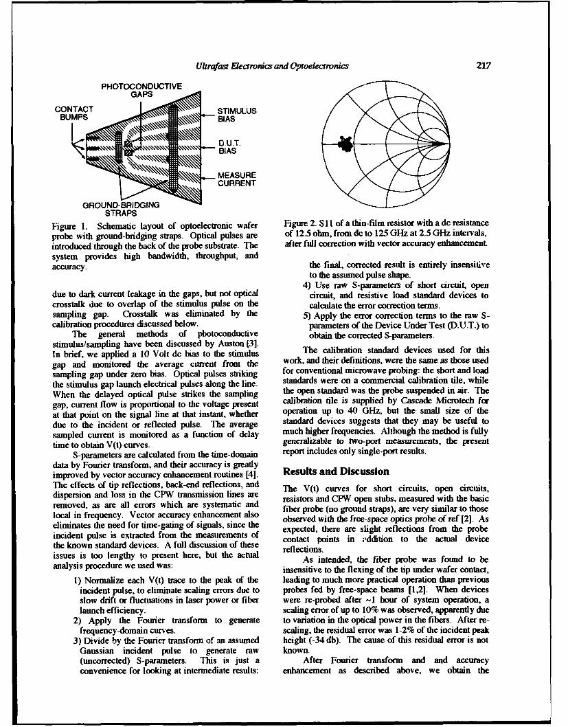
Ufrrafasr Electronics and Optoelectronics 217
PHOTOCONDUCTIVEGAPS
CONTACT STIMULUSBUMPS BIAS
��O.U.T. *'-BIAS
MEASURECURRENT
GROUND-BRIDGING
STRAPS
Figure 1. Schematic layout of optoelectronic wafer Figure 2. SI I of a thin-film resistor with a dc resistance
probe with ground-bridging straps. Optical pulses are of 12.5 ohm, from dc to 125 GHz at 2.5 GHz intervals,
introduced through the back of the probe substrate. The after full correction with vector accuracy enhancement.
system provides high bandwidth, throughput, andaccuracy. the final, corrected result is entirely insensitive
to the assumed pulse shape.4) Use raw S-parameters of short circuit, open
due to dark current leakage in the gaps, but not optical circuit, and resistive load standard devices tocrosstalk due to overlap of the stimulus pulse on the calculate the error correction terms.sampling gap. Crosstalk was eliminated by the 5) Apply the error correction terms to the raw S-calibration procedures discussed below, parameters of the Device Under Test (D.U.T.) to
The general methods of photoconductive obtain the corrected S-parameters.stimulus/sampling have been discussed by Auston [31.In brief, we applied a 10 Volt dc bias to the stimulus The calibration standard devices used for thisgap and monitored the average current from the work, and their definitions, were the same as those usedsampling gap under zero bias. Optical pulses striking for conventional microwave probing: the short and load
the stimulus gap launch electrical pulses along the line. standards were on a commercial calibration tile, while
When the delayed optical pulse strikes the sampling the open standard was the probe suspended in air. The
gap, current flow is proportional to the voltage present calibration tile is supplied by Cascade Mcrotech for
at that point on the signal line at that instant, whether operation up to 40 GHz, but the small size of the
due to the incident or reflected pulse. The average standard devices suggests that they may be useful to
sampled current is monitored as a function of delay much higher frequencies. Although the method is fully
time to obtain V(t) curves. generalizable to two-port measurements, the present
S-parameters are calculated from the time-domain report includes only single-port results.
data by Fourier transform, and their accuracy is greatlyimproved by vector accuracy enhancement routines [4]. Results and DiscussionThe effects of tip reflections, back-end reflections, and The V(t) curves for short circuits, open circuits,dispersion and loss in the CPW transmission lines are resistors and CPW open stubs, measured with the basicremoved, as are all errors which are systematic and fiber probe (no ground straps), are very similar to thoselocal in frequency. Vector accuracy enhancement also observed with the free-space optics probe of ref [2]. Aseliminates the need for time-gating of signals, since the expected, there are slight reflections from the probeincident pulse is extracted from the measurements of contact points in :,ddition to the actual devicethe known standard devices. A full discussion of these reflections.issues is too lengthy to present here, but the actual ins.As intended, the fiber probe was found to beanalysis procedure we used was: insensitive to the flexing of the tip under wafer contact,
1) Normalize each V(t) trace to the peak of the leading to much more practical operation than previousincident pulse, to eliminate scaling errors due to probes fed by free-space beams [1,21. When devicesslow drift or fluctuations in laser power or fiber were re-probed after -1 hour of system operation, alaunch efficiency. scaling error of up to 10% was observed, apparently due
2) Apply the Fourier transform to generate to variation in the optical power in the fibers. After re-frequency-domain curves. scaling, the residual error was 1-2% of the incident peak
3) Divide by the Fourier transform of an assumed height (-34 db). The cause of this residual error is notGaussian incident pulse to generate raw known.(uncorrected) S-parameters. This is just a After Fourier transform and and accuracyconvenience for looking at intermediate results: enhancement as described above, we obtain the
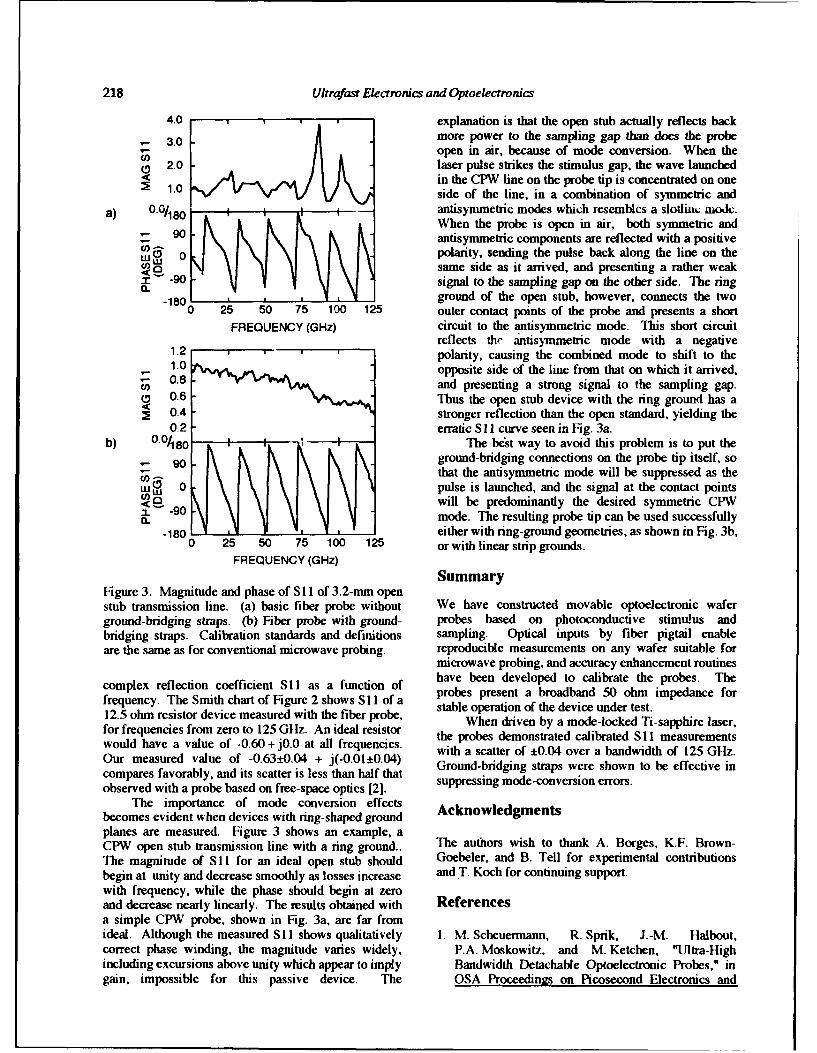
218 Ultrafast Electronics and Optoelectronics
4.0 . *explanation is that the open stub actually reflects back
3.0 more power to the sampling gap than does the probeopen in air, because of mode conversion. When the
2.0 laser pulse strikes the stimulus gap, the wave launched< in the CPW line on the probe tip is concentrated on one• 1.0 side of the line, in a combination of symmetric and
a) 0"0/1 80 - antisynnmetric modes whkih resemblcs a slotinc, mode.When the probe is open in air, both symmetric andantisymmetric components are reflected with a positive
W 0 polarity, sending the pulse back along the line on thesame side as it arrived, and presenting a rather weak
X: -tovsignal to the sampling gap on the other side. The ring-1801 ground of the open stub, however, connects the two
0 25 50 75 100 125 outer contact points of the probe and presents a shortFREQUENCY (GHz) circuit to the antisymmetric mode. This short circuit
reflects the antisymmnetric mode with a negative1.2 polarity, causing the combined mode to shift to the1.0 •opposite side of the line from that on which it arrived,0.8 and presenting a strong signal to the sampling gap.
3 0.6 Thus the open stub device with the ring ground has a2 0.4 stronger reflection than the open standard, yielding the
02 erratic S 11 curve seen in Fig. 3a.b) 0-0180• •The best way to avoid this problem is to put the
S90 -ground-bridging connections on the probe tip itself, sothat the antisymmetric mode will be suppressed as the
S(9 0 .pulse is launched, and the signal at the contact points<!a -will be predominantly the desired symmetric CPWQ. I -o mode. The resulting probe tip can be used successfully
-180 - either with ring-ground geometries, as shown in Fig. 3b,0 25 50 75 100 125 or with linear strip grounds.
FREQUENCY (GHz)Summary
Figure 3. Magnitude and phase of S 1I of 3.2-mnm open
stub transmission line. (a) basic fiber probe without We have constructed movable optoelectronic waferground-bridging straps. (b) Fiber probe with ground- probes based on photoconductive stimulus andbridging straps. Calibration standards and definitions sampling. Optical inputs by fiber pigtail enableare the same as for conventional microwave probing. reproducible measurements on any wafer suitable for
microwave probing, and accuracy enhancement routines
complex reflection coefficient SII as a function of have been developed to calibrate the probes. The
frequency. The Smith chart of Figure 2 shows S 1I of a probes present a broadband 50 ohm impedance for
12.5 ohm resistor device measured with the fiber probe, stable operation of the device under test.
for frequencies from zero to 125 GHz. An ideal resistor t When driven by a mode-locked Ti-sapphire laser,would frequenvies aromuero tof -0 + . at ieall freq ciest the probes demonstrated calibrated S 1I measurementswould have a value of -0.60 + j0.0 at all frequencies, with a scatter of ±0.04 over a bandwidth of 125 GHz.Our measured value of -0.63±-0.04 + j(-0.0l+0.04) Gron-rdigsrp eesont eefciei
compares favorably, and its scatter is less than half that round-bridging straps were shown to be effective in
observed with a probe based on free-space optics [2]. suppressing mode-conversion errors.
The importance of mode conversion effects Acknowledgmentsbecomes evident when devices with ring-shaped groundplanes are measured. Figure 3 shows an example, aCPW open stub transmission line with a ring ground.. The authors wish to thank A. Borges, K.F. Brown-The magnitude of S I I for an ideal open stub should Goebeler, and B. Tell for experimental contributionsbegin at unity and decrease smoothly as losses increase and T. Koch for continuing support.with frequency, while the phase should begin at zeroand decrease nearly linearly. The results obtained with Referencesa simple CPW probe, shown in Fig. 3a, are far fromideal. Although the measured S 11 shows qualitatively 1. M. Scheuermann, R. Sprik, J.-M. Halbout,correct phase winding, the magnitude varies widely, P.A. Moskowitz, and M. Ketchen, "Ultra-Highincluding excursions above unity which appear to imply Bandwidth Detachable Optoelectronic Probes," ingain, impossible for this passive device. The OSA Proceedings on Picosecond Electronics and
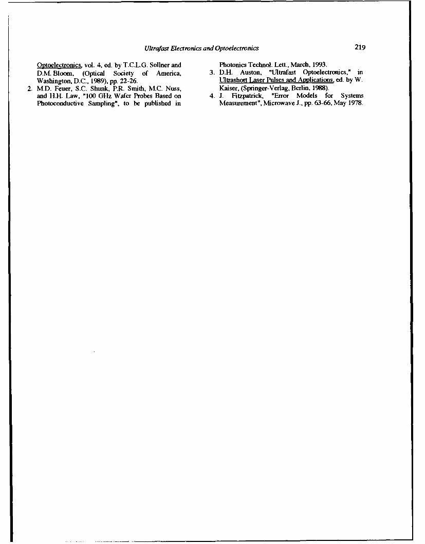
Ultrafast Electronics and Optoelectronics 219
Optoelectronics, vol. 4, ed. by T.C.L.G. Sollner and Photonics Technol. Lett., March, 1993.D.M. Bloom. (Optical Society of America, 3. D.H. Auston, "Ultrafast Optoelectronics," inWashington, D.C., 1989), pp. 22-26. Ultrashort Laser Pulses and Applications ed. by W.
2. M.D. Feuer, S.C. Shunk, P.R. Smith, M.C. Nuss, Kaiser, (Springer-Verlag, Berlin. 1988).and H.H. Law, "100 GHz Wafer Probes Based on 4. 1. Fitzpatrick, "Error Models for SystemsPhotoconductive Sampling", to be published in Measurement", Microwave J., pp. 63-66, May 1978.
Electro-Optic Sampling of High Speed NonlinearDevices
Kok Wai Chang and Wayne V. Sorin
Hewlett-Packard Laboratories, Palo Alto, California 94303
Abstract reduce the common-mode amplitude noise of a gain-An electrooptic measurement system which combines switched laser-diode-based EO sampling system [7].the advantages of equivalent-time sampling with The elimination of the amplitude noise allowed thedifferential detection is used for the characterization of offset frequency to be reduced. In this paper we reporthigh speed nonlinear electronic devices, on an electrooptic sampling system based on a fiber-
grating-compressed Nd:YAG mode-locked laser with2 ps of temporal resolution that combines the
This paper addresses the characterization of high- advantages of both the fast-offset/averaging detectionspeed nonlinear devices using direct and indirect scheme and the differential detection scheme for theelectrooptic (EO) sampling. In order to overcome the characterization of high speed nonlinear devices suchlarge low-frequency amplitude noise of the pulsed as SRDs, RTDs and SRD-driven nonlinearlaser, previous electrooptic measurement systems [1-5] transmission lines.employed AM modulation to detect the EO signal at Fig.l shows the experimental setup for the mode-frequencies where the amplitude noise dropped below locked Nd:YAG laser and fiber-grating pulse-the shot noise. However, the characteristics of many compressor-based electrooptic sampling system whichhigh speed nonlinear devices such as Step Recovery uses an GaAs probe tip as a indirect longitudinalDiodes (SRDs), Resonant Tunneling Diodes (RTDs) electric field sensor. The incident and refklcted beamsand SRD-driven nonlinear transmission lines do not are separated by manipulation of their polarization [6]function properly when their input signals are chopped in such a way that the reflected beam produces a linearand therefore cannot be characterized by this signal polarization inclined at 45 degrees to the axes of thedetection scheme. polarization bcamsplitters when there is no applied
A fast-offset/averaging detection scheme [6] for EO field on the GaAs probe tip. The reflected beamsampling systems has been proposed to avoid polarization state will become inclined at 45 + 6signal chopping for the testing of devices that are degrees to the axes of the polarization beamsplitterssensitive to external AM modulation. This detection when there is an longitudinal electric field overlappingscheme is similar to equivalent-time sampling [6] the GaAs probe tip. The vertical component is directedexcept that the offset frequency is increased to a value by the first polarization beamsplitter onto the firstwhere the amplitude noise drops below the shot noise. photodiode. The horizontal component is rotated byFor may lasers this means an offset frequency Af of the Faraday rotator and the half wave plate to become500 kHz or greater. The large offset frequency vertically polarized and is then directed by the secondimposes a relatively large measurement bandwidth of polarization beamsplitter onto the second photodiode.25 MHz or more for testing nonlinear devices that A differential amplifier is then used to amplify thegenerate 50 or more harmonics. This degrades photocurrents from the two photodiodes and tosensitivity since larger bandwidth and higher noise suppress the common-mode intensity noise. Thereceivers must be used. Recently this signal detection amount of common-mode rejection is measured by ascheme was used together with differential detection to low frequency RF spectrum analyzer.
OSA Proceedkg on Ukrafast Elecronics and OptoeIecfronkcs 199, VoL 14 220Jagdeep Shah and Uneh Mishra (edL)0 1993 Optical Society ofAmerica
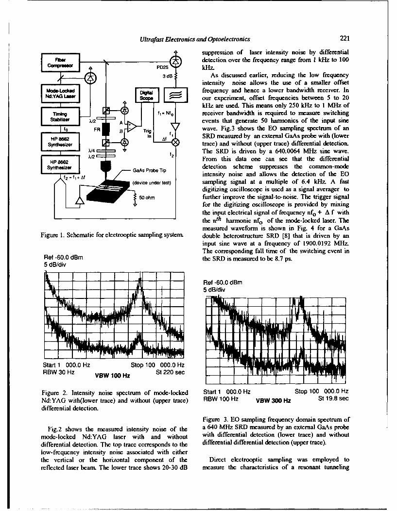
Ultrafast Electronics and Optoelectronics 221
suppression of laser intensity noise by differentialFiber detection over the frequency range from 1 kHz to 100
3 dB As discussed earlier, reducing the low frequency"intensity noise allows the use of a smaller offset
Mode-Locked DVW frequency and hence a lower bandwidth receiver. InNd:YAG Law Scope our experiment, offset frequencies between 5 to 20
kHz are used. This means only 250 kHz to 1 M]z ofTmn = Nfo receiver bandwidth is required to measure switching
Stblie Aevents that generate 50 harmonics of the input sineIf° FR B- Twave. Fig.3 shows the EO sampling spectrum of an
InHP 8'6 I SRD measured by an external GaAs probe with (lowerSynthesizer trace) and without (upper trace) differential detection.
I V4 --- The SRD is driven by a 640.0064 MHz sine wave.HP8V662 I V/2 2From this data one can see that the differential
Synthesizer GaAs Probe Tip detection scheme suppresses the common-mode
12 = 1 + Afintensity noise and allows the detection of the EQ(device under test) sampling signal at a multiple of 6.4 kHz. A fast
digitizing oscilloscope is used as a signal averager to50 ohm further improve the signal-to-noise. The trigger signal
for the digitizing oscilloscope is provided by mixingthe input electrical signal of frequency nfo + A f with
the nth harmonic nfo of the mode-locked laser. Themeasured waveform is shown in Fig. 4 for a GaAs
Figure 1. Schematic for electrooptic sampling system. double heterostructure SRD [8] that is driven by aninput sine wave at a frequency of 1900.0192 MHz.The corresponding fall time of the switching event in
Ref -60.0 dBm the SRD is measured to be 8.7 ps.5 dB/div
k 1- - - - Ref -60.0OdBm
i N ...
-.-.- - - ' - -I 'd Ldiv
Start 1 000.0 Hz Stop 100 000.0 HzRBW 30 Hz VBW 100 Hz St 220 sec
Figure 2. Intensity noise spectrum of mode-locked Start 1 000.0 Hz Stop 100 000.0 HzNd:YAG with(lower trace) and without (upper trace) RBW 100 Hz VBW 300 Hz St 19.8 sec
differential detection.
Figure 3. EO sampling frequency domain spectrum of
Fig.2 shows the measured intensity noise of the a 640 MHz SRD measured by an external GaAs probe
modc-locked Nd:YAG laser with and without with differential detection (lower trace) and without
differential detection. The top trace corresponds to the differential differential detection (upper trace).
low-frequency intensity noise associated with eitherthe vertical or the horizontal component of the Direct electrooptic sampling was employed toreflccted laser beam. The lower trace shows 20-30 dB measure the characteristics of a resonant tunneling
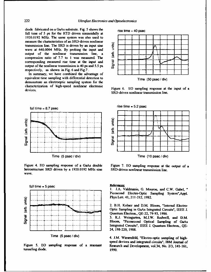
222 Ultrafast Flectronics and Optoelectronics
diode fabricated on a GaAs substrate. Fig. 5 shows the rise time = 40 psecfall time of 5 ps for the RTD driven sinusoidally at1920.0192 MHz. The same system was also used tomeasure the characteristics of an SRD-driven nonlineartransmission line. The SRD is driven by an input sinewave at 640.0064 MHz By probing the input and "output of the nonlinear transmission line, a -e - : .... -"
compression ratio of 7.7 to 1 was measured. The - :- : --- - - -corresponding measured rise time at the input and ,
output of the nonlinear transmission is 40 ps and 5.5 ps CDrespectively, as shown in Fig. 6 and Fig.7. - -
In summary, we have combined the advantage of , -
equivalent time sampling with differential detection to Time (50 psec / div)demonstrate an electrooptic sampling system for thecharacterization of high-speed nonlinear electronic Figure 6. EQ sampling response at the input of adevices. SRD-driven nonlinear transmission line.
fall time = 8.7 p rise time = 5.2 psec
.. .. .. .. .. .. . .. . .. .. . ... ... ...... ..
... ..-...... .-.......... .... . ... -.... ... ... . .. . . . .... ... . ..... . \ - ...-.......... . .........
0. . ........ .......... , . . =.(~5 .U)S. ................... .. ... ......... i .......... : ...... • ........ ......... .....
Time (5 psec/ div) Time (10 psec /div)
Figure 4. EO sampling response of a GaAs double Figure 7. EO sampling response at the output of ahetrostructure SRD driven by a 1920.0192 MHz sine SRD-driven nonlinear transmission line.wave.
fall time = 5 psec1. J.A. Valdmanis, G. Mourou, and C.W. Gabel,"
I :Picoscond Electro-Optic Sampling System",Appl.Phys Lett. 41, 211-212, 1982.
C--- ..... : ........................................ 2. B.FL Kolner and D.M. Bloom, "Internal Electro-
c .. ......... .......... ......... . ......... . Optic Sampling in GaAs Integrated Circuits", IEEE J.Quantum Electron., QE-22, 79-93, 1986.
C 3. KJ. Weingarten, M.J.W. Rodwell, and D.M.Cn Bloom, "Picosecond Optical Sampling of GaAs. ........... ..................... ........... .......... .......... Integrated Circuits", IEEE J. Quantum Electron., QE-
L 24, 198-220, 1988.
Time (5 psec/ div) 4. J.M. Wiesenfeld, "Electro-optic sampling of high-
speed devices and integrated circuits", IBM Journal ofFigure 5. EO sampling response of a resonant Research and Development, vol.34, No. 2/3, 141-161,tunneling diode. 1990.
Ultrafast Electronics and Optoelectronics 223
5. R. Shinagawa and T. Nagatsuma, "A Laser-Diode- Dec. 1987.Based Picosecond Electro-Optic Prober for High-Speed LSIs", IEEE Trans. Instrum. Meas., Vol. 41, 7. T. Nagatsuma, MK Yaita and K. Shinagawa,No. 3, 375-380, 1992. "External Electro-optic Sampling Using Poled
Polymers". sumnitted to Japn. J. Appl. Phys.6. K.J. Weingarten, "Galium Arsenide IntegratedCircuit Testing Using Electrooptic Sampling", PhD. 8. M.R.T. Tan, S.T. Wang, D.E. Mars and J.L. Moll,Thesis, Edward L. Ginzton Laboratory of the W.W. "12 ps GaAs Double Heterostructure step recoveryHansen Laboratories of Physics, Standford University, diode", Electron. Lett., Vol. 28, 673-675, 1992.
120-GHz-Bandwidth Characterization of Microwave PassiveDevices Using External Silicon-On-Sapphire Photoconductive
Sampling Probe
J. Kim, J. Son, S. Wakana*, J. Nees, S. Williamson, J. Whitaker, and G. Mourou
Center for Ulkrafast Optical Science, University of Michigan, 2200 Bonisteel, 1006 IST,Ann Arbor, Michigan 48109-2099
*S. Wakana is also at Fujitsu Laboratory Ltd.
Introduction The technique is based on high-impedance
external sampling with 2.1-ps temporal resolution, 8-
Conventional purely electronic measurement g.m spatial resolution and high signal-to-noise ratio.
instruments such as vector network analyzers, spectrum The measurement point can be very close to the device
analyzers and sampling oscilloscopes are not effective at under test. Therefore, the technique minimizes
above 100 GHz. One major limitation is imposed by interconnection discontinuities and consequently errors
the connectors and waveguides needed for signal and uncertainties from device de-embedding procedures.
coupling between the test instrument and the device To demonstrate the capability of the photoconductive
under test. To overcome those limitations of present probe sampling technique for nun-wave circuit testing,
measurement techniques, we have developed a we applied tie technique to characterize nun-wave band-
photoconductive probe sampling technique which can be block filters and phase delay lines which are being used
applied to the measurement of S-parameters cf mm- in MMICs up to 200 Gllz.
wave circuit components with a 120-GHz measurement
bandwidth [1). The photoconductive probe sampling
technique combines the ultrafast optical technology of Experiments and results
120-fs Ti-Sapphire short pulse laser [2] and
microfabrication technology of Silicon-On-Sapphire Figure. 1 is an SEM picture of the
(SOS) photoconductive sampling probe, which consists photoconductive(PC) sampling probe. It consists of a
of a high-impedance interdigitated photoconductive high impedance metal-semiconductor-metal (MSM)
switch. The probe technology has demonstrated a 2.1 ps photoconductive switch on a damaged Silicon-On-
temporal resolution and low-invasiveness making this Sapphire substrate and a Ti contact lip of 3-tim height.
very attractive for external circuit testing of mm-wave Figure.2 shows the experimental set-up used to measure
circuits with a 120-GHz measurement bandwidth. the characteristics of band-block filters of microstripline
OSA Procea1''P -6 Uhrqafw Eecvc•and wOProeLectrf.,cAd 1993, Vol. 14 224Jaw-p kah m•d U-a, MLiA (eA)0 1993 Qp4aI Sodaty qf Arxcaz
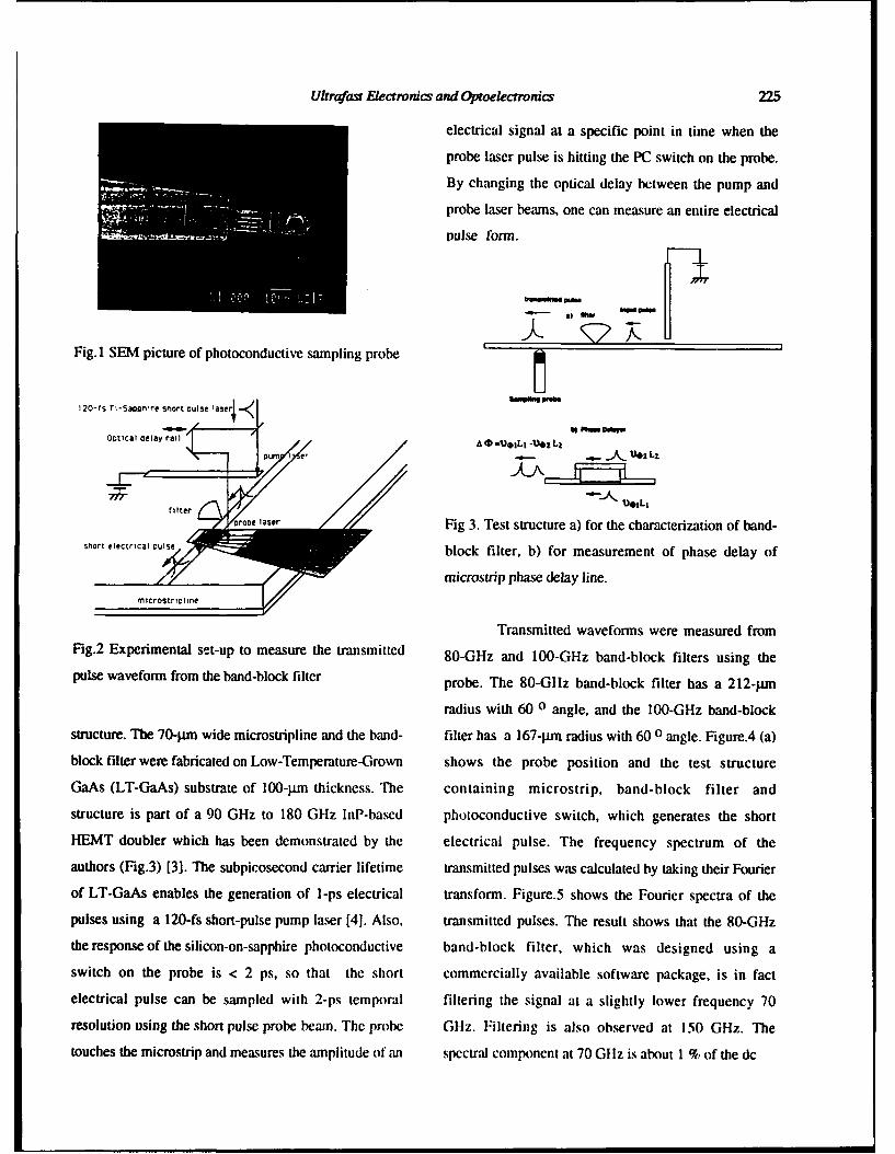
Ultrafast Electronics and Optoelectronics 225
electrical signal at a specific point in time when the
probe laser pulse is hitting the PC switch on the probe.
By changing the optical delay between the pump and
probe laser beams, one can measure an entire electrical
pulse form.
I,,il Hlw" man
SI) BIMW MIPP-
Fig. 1 SEM picture of photoconductive sampling probe
120-fS rI-Sagore Srhort gulse ýaser
ODtlcal delay r il Ai)sOII.•lL
PA0l)rL e, U2LL2
filter
pr~o, laser Fig 3. Test structure a) for the characterization of band-sh~ort electrical pulse block filter, b) for measurement of phase delay of
z 1/microstrip phase delay line.microstriotine
Transmitted waveforms were measured fromFig.2 Experimental set-up to measure the transmitted 80-GHz and 100-GHz band-block filters using the
pulse waveform from the band-block filter probe. The 80-GHz band-block filter has a 212-jum
radius with 60 0 angle, and the 100-GHz band-block
structure. The 70-pm wide microstripline and the band- filter has a 167-pjm radius with 60 0 angle. Figure.4 (a)
block filter were fabricated on Low-Temperature-Grown shows the probe position and the test structure
GaAs (LT-GaAs) substrate of 100-jim thickness. The containing microstrip, band-block filter and
structure is part of a 90 GHz to 180 GHz laP-based photoconductive switch, which generates the short
HEMT doubler which has been demonstrated by the electrical pulse. The frequency spectrum of the
authors (Fig.3) [3]. The subpicosecond carrier lifetime transmitted pulses was calculated by taking their Fourier
of LT-GaAs enables the generation of I-ps electrical transform. Figure.5 shows the Fourier spectra of the
pulses using a 120-fs short-pulse pump laser [4]. Also, transmitted pulses. The result shows that the 80-GHz
the response of the silicon-on-sapphire photoconductive band-block filter, which was designed using a
switch on the probe is < 2 ps, so that the short commercially available software package, is in fact
electrical pulse can be sampled with 2-ps temporal filtering the signal at a slightly lower frequency 70
resolution using the short pulse probe beam. The probe GHz. Filtering is also observed at 150 GHz. The
touches the microstrip and measures the amplitude of an spectral component at 70 GlIz is about I % of the dc
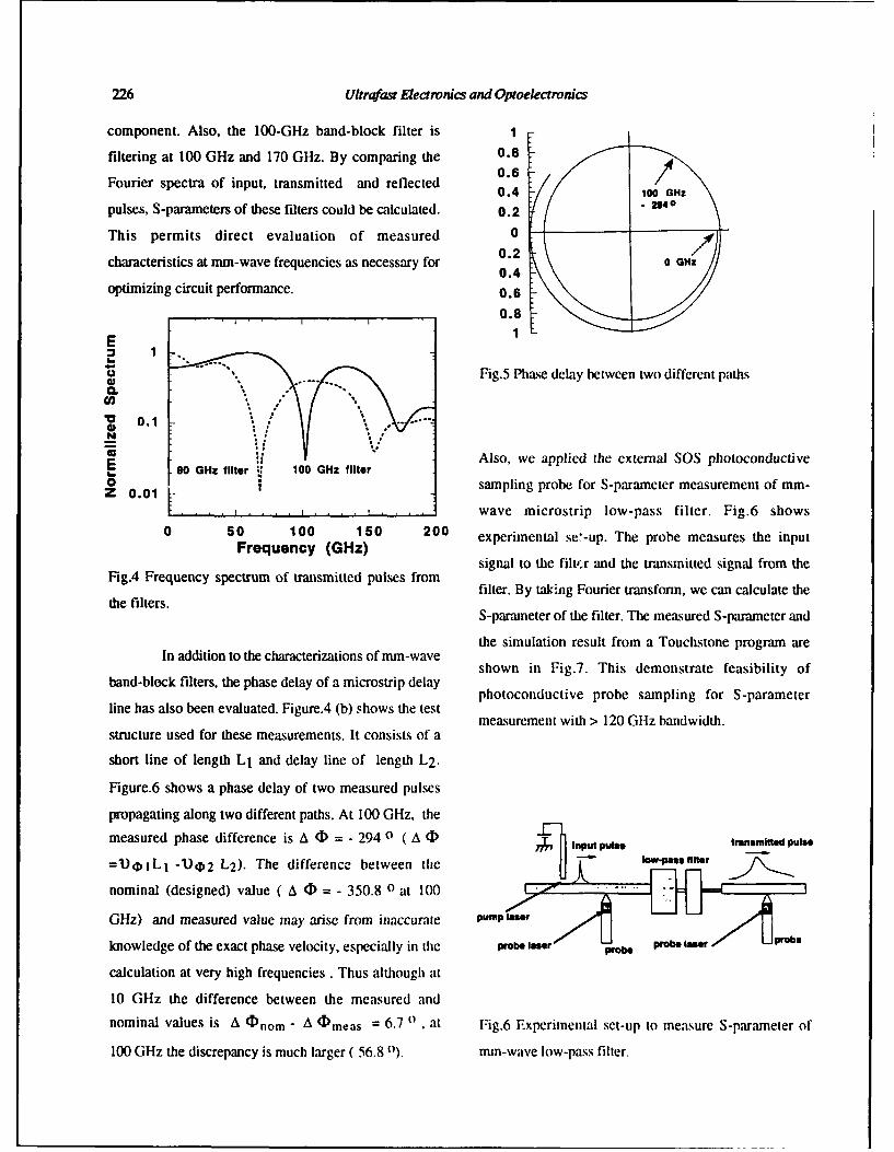
226 Ultrafast Electronics and Optoelectronics
component. Also, the 100-GHz band-block filter is 1
filtering at 100 GHz and 170 GHz. By comparing the 0.8
Fourier spectra of input, transmitted and reflected 0.4 a
pulses, S-parameters of these filters could be calculated. 0.2 2140
This permits direct evaluation of measured 0
characteristics at umm-wave frequencies as necessary for 0.2 40.4
optimizing circuit performance. 0.6
S, . . . . , _ _ _, 0 .8
E 1
o_ Fig.5 Phase delay between two different pathsCL
0.1
* Also, we applied the external SOS photoconductiveE 80 GHz filter • 100 GHz filtero |sampling probe for S-parameter measurement of mm-Z 0.01 L-
. . . .. wave microstrip low-pass filter. Fig.6 shows
0 50 100 150 200 experimental se'-up. The probe measures the inputFrequency (GHz)
signal to the filtmr and the transmitted signal from theFig.4 Frequency spectrum of transmitted pulses from filter. By takinag Fourier transform, we can calculate the
the filters.S-parameter of the filter. The measured S-parameter and
the simulation result from a Touchstone program areIn addition to the characterizations of ram-waveshown in Fig.7. This demonstrate feasibility of
band-block filters, the phase delay of a microstrip delay photoconductive probe sampling for S-parameter
line has also been evaluated. Figure.4 (b) shows the test measurement with > 120 Gltz bandwidth.
structure used for these measurements. It consists of a
short line of length L1 and delay line of length L2.
Figure.6 shows a phase delay of two measured pulses
propagating along two different paths. At 100 GHz, the
measured phase difference is A (D = - 294 o ( A ( I Pt tp
=: ,jILI -)4> 2 L2 ). The difference between the low-pass-finer
nominal (designed) value ( A (D - 350.8 0 at 100 -
GHz) and measured value may arise from inaccurate pumIp laser
knowledge of the exact phase velocity, especially in the probe laser pro" probe WSW
calculation at very high frequencies . Thus although at
10 GHz the difference between the measured and
nominal values is A 4 ) nom - A ( ) mneas = 6.7 o at Fig.6 Experimental set-up to measure S-parameter of
100 GHz the discrepancy is much larger ( 56.8 0). mm-wave low-pass filter.
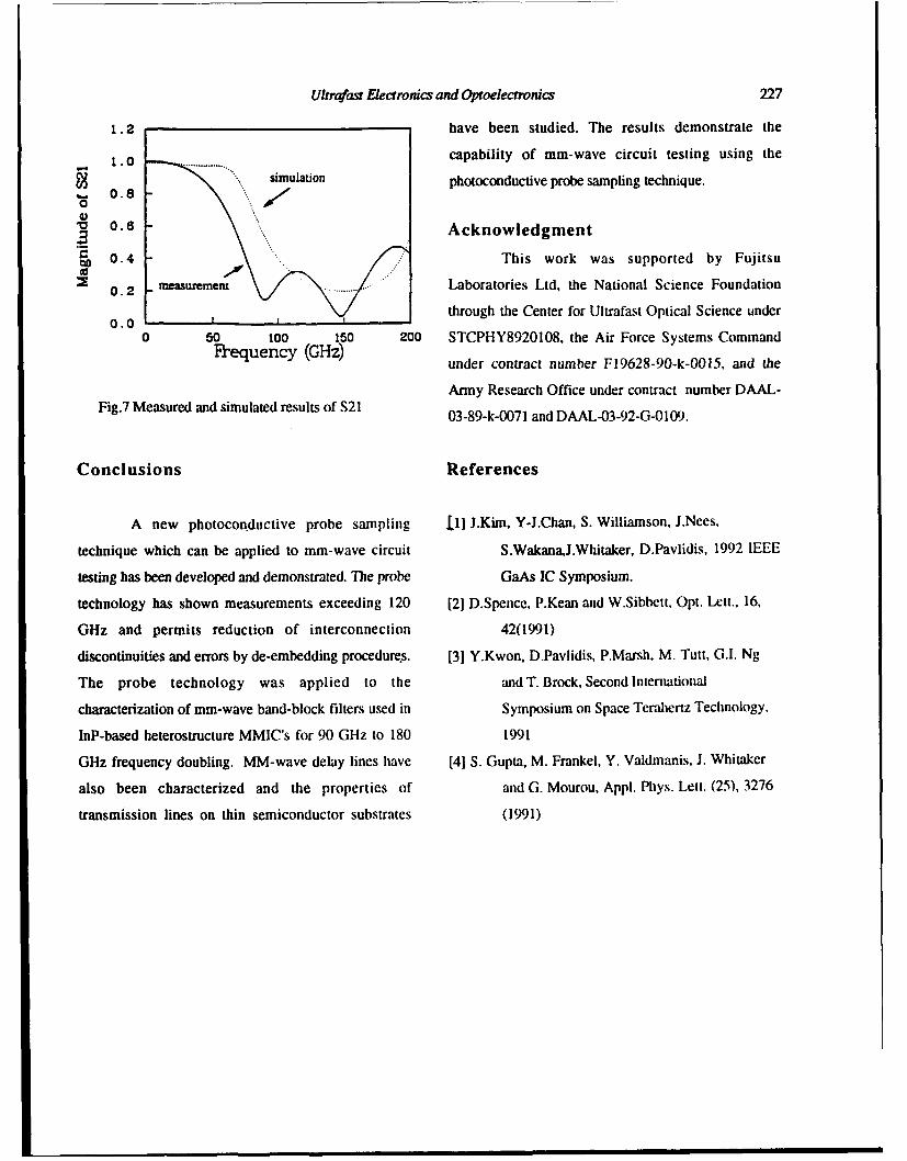
Ultrafast Electronics and Optoelectronics 227
1.2 have been studied. The results demonstrate the
1.0 .............. capability of mm-wave circuit testing using the
simulation photoconductive probe sampling technique., 0.8
0.6
o 0.8 Acknowledgment
"-0.4 This work was supported by Fujitsu
0. 2 measurement Laboratories Ltd, the National Science Foundation
0.0 2 through the Center for Ultrafast Optical Science under
0 50 100 150 200 STCPHY892010g, the Air Force Systems Commandfrequency (GHz) under contract number F19628-90-k-0015, and the
Army Research Office under contract number DAAL-Fig.7 Measured and simulated results of S21 03-89-k-0071 and DAAL-03-92-G-0109.
Conclusions References
A new photoconductive probe sampling [I] J.Kim, Y-J.Chan, S. Williamson, J.Nees,
technique which can be applied to mm-wave circuit S.WakanaJ.Whitaker, D.Pavlidis, 1992 IEEE
testing has been developed and demonstrated. The probe GaAs IC Symposium.
technology has shown measurements exceeding 120 [2] D.Spence, P.Kean and W.Sibbett, Opt. Lett., 16,
GHz and permits reduction of interconnection 42(1991)
discontinuities and errors by de-embedding procedures. [31 Y.Kwon, D.Pavlidis, P.Marsh, M. Tutt, G.I. Ng
The probe technology was applied to the and T. Brock, Second International
characterization of mm-wave band-block filters used in Symposium on Space Terahertz Technology,
InP-based heterostructure MMIC's for 90 GHz to 180 1991
GHz frequency doubling. MM-wave delay lines have [4] S. Gupta, M. Frankel, Y. Valdmanis, J. Whitaker
also been characterized and the properties of and G. Mourou, Appl. Phys. Lett. (25), 3276
transmission lines on thin semiconductor substrates (1991)
Superconductors
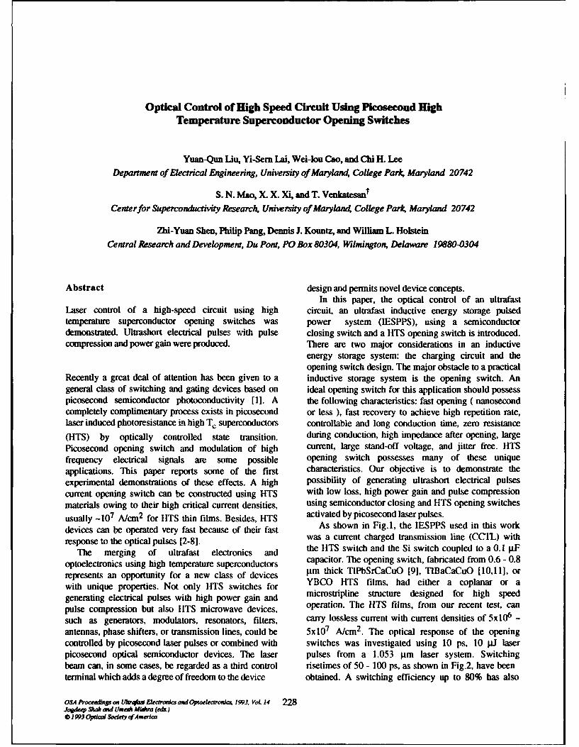
Optical Control of High Speed Circuit Using Picosecond HighTemperature Superconductor Opening Switches
Yuan-Qun Liu, Yi-Sem Lai, Wei-lou Cao, and Chi H. LeeDepartment of Electrical Engineering, University of Maryland, College Park, Maryland 20742
S. N. Mao, X. X. Xi, and T. VenkatesantCenterfor Superconductivity Research, University of Maryland. College Park; Maryland 20742
7hi-Yuan Shen, Philip Pang, Dennis J. Kountz, and William L. HolsteinCentral Research and Development, Du Pont, PO Box 80304, Wilmington, Delaware 19880-0304
Abstract design and permits novel device concepts.In this paper, the optical control of an ultrafast
Laser control of a high-speed circuit using high circuit, an ultrafast inductive energy storage pulsedtemperature superconductor opening switches was power system (IESPPS), using a semiconductordemonstrated. Ultrashort electrical pulses with pulse closing switch and a HTS opening switch is introduced.compression and power gain were produced. T"here are two major considerations in an inductive
energy storage system: the charging circuit and theopening switch design. The major obstacle to a practical
Recently a great deal of attention has been given to a inductive storage system is the opening switch. Angeneral class of switching and gating devices based on ideal opening switch for this application should possesspicosecond semiconductor photoconductivity [1]. A the following characteristics: fast opening ( nanosecondcompletely complimentary process exists in picosecond or less ), fast recovery to achieve high repetition rate,laser induced photoresistance in high T. superconductors controllable and long conduction time, zero resistance(HTS) by optically controlled state transition. during conduction, high impedance after opening, largePicosecond opening switch and modulation of high current, large stand-off voltage, and jitter free. HTSfrequency electrical signals are some possible opening switch possesses many of these uniqueapplications. This paper reports some of the first characteristics. Our objective is to demonstrate theexperimental demonstrations of these effects. A high possibility of generating ultrashort electrical pulsescurrent opening switch can be constructed using HTS with low loss, high power gain and pulse compressionmaterials owing to their high critical current densities, using semiconductor closing and HTS opening switches
usually -107 A/cm 2 for HTS thin films. Besides, HTS activated by picosecond laser pulses.
devices can be operated very fast because of their fast As shown in Fig.1, the IESPPS used in this work
response to the optical pulses [2-8]. was a current charged transmission line (CCTL) withThe merging of ultrafast electronics and the HTS switch and the Si switch coupled to a 0.1 gF
optoelectronics using high temperature superconductors capacitor. The opening switch, fabricated from 0.6 - 0.8
represents an opportunity for a new class of devices pm thick TIPbSrCaCuO [9], TIBaCaCuO [10,11], orwith unique properties. Not only HTS switches for YBCO HTS films, had either a coplanar or a
generating electrical pulses with high power gain and microstripline structure designed for high speedpulse compression but also HTS microwave devices, operation. The HTS films, from our recent test, cansuch as generators, modulators, resonators, filters, carry lossless current with current densities of 5x10 6 -antennas, phase shifters, or transmission lines, could be 5x10 7 A/cm 2. The optical response of the openingcontrolled by picosecond laser pulses or combined with switches was investigated using 10 ps, 10 pJ laserpicosecond optical semiconductor devices. The laser pulses from a 1.053 gm laser system. Switchingbeam can, in some cases, be regarded as a third control risetimes of 50 - 100 ps, as shown in Fig.2, have beenterminal which adds a degree of freedom to the device obtained. A switching efficiency up to 80% has also
OSA Proceedinp on U4*aqw Electronics and OeLtOeectronh 1993, VoL 14 228Jagdeep s9h and UmeA Msha (ed& )0 1993 Optical Sod aty of Amerca
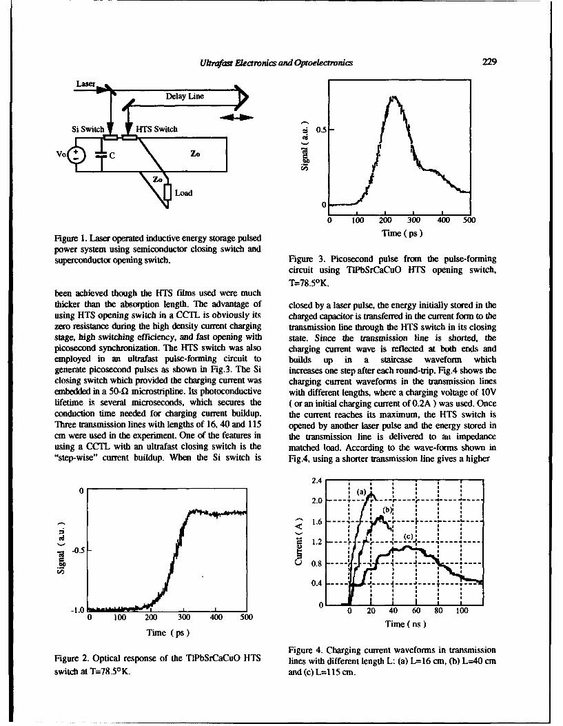
Ultrafast Electronics and Oproelectronics 229
Laser-Delay Line
Si Switch HTS Switch : 0.5
Vo + o 0 10
Z jo
0 100 200 300 400 500
Figure 1. Laser operated inductive energy storage pulsed Time ( ps)
power system using semiconductor closing switch andsuperconductor opening switch. Figure 3. Picosecond pulse from the pulse-forming
circuit using TIPbSrCaCuO HTS opening switch,T=78.50 K.
been achieved though the HTS films used were muchthicker than the absorption length. The advantage of closed by a laser pulse, the energy initially stored in theusing HTS opening switch in a CCTL is obviously its charged capacitor is transferred in the current form to thezero resistance during the high density current charging transmission line through the HTS switch in its closingstage, high switching efficiency, and fast opening with state. Since the transmission line is shorted, thepicosecond synchronization. The HTS switch was also charging current wave is reflected at both ends andemployed in an ultrafast pulse-forming circuit to builds up in a staircase waveform whichgenerate picosecond pulses as shown in Fig.3. The Si increases one step after each round-trip. Fig.4 shows theclosing switch which provided the charging current was charging current waveforms in the transmission linesembedded in a 50-41 microstripline. Its photoconductive with different lengths, where a charging voltage of IOVlifetime is several microseconds, which secures the ( or an initial charging current of 0.2A ) was used. Onceconduction time needed for charging current buildup. the current reaches its maximum, the HTS switch isThree transmission lines with lengths of 16, 40 and 115 opened by another laser pulse and the energy stored incm were used in the experiment. One of the features in the transmission line is delivered to an impedanceusing a CCTL with an ultrafast closing switch is the matched load. According to the wave-forms shown in"step-wise" current buildup. When the Si switch is Fig.4, using a shorter transmission line gives a higher
2.4 - 1 I
0 : (a)2.0 . -
S 1.6 .. .- . . r.. .".. . . .S*lI " I
* I '' I I I
01.6 -- ------------0.5-
0.4 ,---,--
-1.0 0 20 40 60 80 1000 100 200 300 400 500
Time ( ns)Time (ps)
Figure 4. Charging current waveforms in transmission
Figure 2. Optical response of the TlPbSrCaCuO HTS lines with different length L: (a) L=16 cm, (b) L--40 cm
switch at T=78.5°K. and (c) L=115 cm.
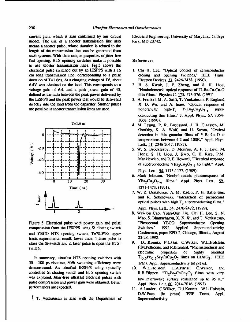
230 U/trafast Eectronimc and OproeLectronics
current gain, which is also confirmed by our circuit Electrical Engineering, University of Maryland, Collegemodel. The use of a shorter transmission lipe also Park, MD 20742.means a shorter pulse, whose duration is related to thelength of the transmission line, can be generated fromsuch systems. With their unique properties of jitter freefast opening, HTS opening switches make it possible Referencesto use shorter transmission lines. Fig.5 shows theelectrical pulse switched out by an IESPPS with a 16 1. Chi H. Lee, "Optical control of semiconductorcm long transmission line, corresponding to a pulse closing and opening switches," IEEE Trans.duration of T=1.6ns. At a charging voltage of IV, about Electron Devices, 37. 2426-2438, (1990).6.4V was obtained on the load. This corresponds to a 2. H. S. Kwok, J. P. Zheng, and S. H. Liou,voltage gain of 6.4, and a peak power gain of 40, "Nonbolometric optical response of Tl-Ba-Ca-Cu-Odefined as the ratio between the peak power delivered by thin films," Physica C, 175. 573-576, (1991).the IESPPS and the peak power that would be delivered 3. A. Frenkel, M. A. Saifi, T. Venkatesan, P. England,directly into the load from the capacitor. Shorter pulses X. D. Wu, and A. Inam, "Optical response ofare possible if shorter transmission lines are used. nongranular high-Tc Y1 Ba2 Cu3 07-O super-
conducting thin films," J. Appl. Phys., 61, 3054-3068, (1990).
T-1.6 4. M. Leung, P. R. Broussard, J. H. Claassen, M.- : : : Osofsky, S. A. Wolf, and U. Strom, "Optical
0 .T- detection in thin granular films of Y-Ba-Cu-O at.. ....... temperatures between 4.2 and 100K," Appl. Phys.
"> -2.0 .. Lett., 5. 2046-2047, (1987).> -2.0 . "...... 5. W. S. Brocklesby, D. Monroe, A. F. J. Levi, M.
S. .-- ----.. +...+...-. .... Hong, S. H. Liou, J. Kwo, C. E. Rice, P.M.S-4.0 . . ..• - Mankiewich, and R. E. Howard, "Electrical responseS* ' " I * * of superconducting YBa 2 Cu3 07 8 to light," Appl.~~~~. ... ... ....- to-,I light," A--p--, ..
-6.0 . "6- Phys. Lett., 54, 1175-1177, (1989).6. Mark Johnson, "Nonbolometric photoresponse of
0 10 20 30 YBa2Cu3 07-8 films," Appl. Phys. Lett., 52,Time (ns) 1371-1373, (1991).
7. W. R. Donaldson, A. M. Kadin, P. H. Ballentine,and R. Sobolewski, "Interaction of picosecondoptical pulses with high Tc superconducting films,"1L 2o t Appl. Phys. Lett., 54, 2470-2472, (1989).
1 2 "8. Wei-lou Cao, Yuan-Qun Liu, Chi H. Lee, S. N.Mao, S. Bhattacharya, X. X. Xi, and T. Venkatesan,
Figure 5. Electrical pulse with power gain and pulse "Picosecond YBCO Superconductor Openingcompression from the IESPPS using Si closing switch Switches," 1992 Applied Superconductivity
and YBCO HTS opening switch, T=78.50 K: upper Conference, paper EPD-2, Chicago, Illinois, Augusttrace, experimental result; lower trace: I laser pulse to 23-28, 1992.close the Si-switch and 2, laser pulse to open the HTS- 9. D.J.Kountz, P.L.Gai, C.Wilker, W.L.Holstein,switch. F.M.Pellicone, and R.Brainard, "Microstructural and
electronic properties of highly orientedIn summary, ultrafast HTS opening switches with T10. 5 Pb0 .5 Sr 2CaCu 2O 7 films on LaAIO 3 ," IEEE
50 - 100 ps risetime, 80% switching efficiency were Trans. Appl. Superconductivity (in press).demonstrated. An ultrafast IESPPS using optically 10. W.L.Holstein, L.A.Parisi, C.Wilker, andcontrolled Si closing switch and HTS opening switch R.B.Flippen, "TI2 Ba2CaCu 2O8 films with verywas explored. Jitter-free ultrafast electrical pulses with low microwave surface resistance up to 95 K,"pulse compression and power gain were obtained. Better Appl. Phys. Lctt. 6&, 2014-2016, (1992).performances are expected. 11. A.Lauder, C.Wilker, DJ.Kountz, W.L.Holstein,
D.W.Face, (in press) IEEE Trans. Appl.t T. Venkatesan is also with the Department of Superconductivity.
Response of a Nb/AI203/Nb Tunnel Junction to PicosecondElectrical Pulses
C. Karadi, S. Verghese, C. A. Mears, J. Orenstein, and P. L. RichardsDepartment of Physics, University of California at Berkeley and Materials Science Division, MS 2-320,
Lawrence Berkeley Laboratory, Berkeley, California 94720
A. T. Barflkecht
Conductus Inc., Sunnyvale, California 94086
Abstract antenna [3]. The silicon was implanted with
l.OxlO15/cm 2 oxygen ions at both 100 keV and 200
We have resolved the time domain response of the keV. The antenna terminals have a 5gm gap whichquasiparticle current in a superconducting tunnel was biased as low as IOV for linear spectroscopy andjunction to picosecond electrical pulses propagating up to 60V for the nonlinear measurements. To excitein free space. the photoconductor we used an unamplified Ti-
Sapphire laser operating at 800nm with 100 fs pulsesand an average power of 50 mW. The use of a high
Introduction repetition rate (100MHz) laser is critical to obtain thehigh ratio of signal to noise in our data. The emitted
The quasiparticle tunneling current in superconductor- electrical pulses are nearly a single cycle with a centerinsulator-superconductor (SIS) junctions has been frequency at approximately 180 GHz and a 3db
exploited in a class of ultrasensitive high-frequency bandwidth of 80 GHz.devies uch as ixes an deectrs 1]. The broadband response of the S15 device is inferreddevices such as mixers and detectors [1] by measuring the dc current induced by interfering two
Nevertheless, the nonlinear, and even linear, response el suric l the juntin, as antin o
of these junctions has not been adequately measured. electrical pulses at the junction, as a function of theWhile SIS junctions have been characterized using cw tm eac ewe hm iueIi ceaiWhurleSs near [21, thae beenchroacterid uesionge nr diagram of the interferometer that was used to perfomsources near 80GHz [2], the broadband response near teemaueet 4.Teple r eeae
the threshold at 2A - eVbias has not been studied. these measurements [4]. The pulses are generated
(Here A is the superconducting gap parameter and from two separate antennas. The beam from each
Vbias is the voltage across the junction) In this work, antenna is partially collimated by a 13mm diameter
we have used picosecond electrical pulses to measure sapphire hypcrhdmisphere and then further collimated
the broadband quasiparticle response of a Nb trilayer by a 3.5 inch diameter f/I parabolic mirror. The two
SIS junction in both the linear and nonlinear regimes. beams are combined into one with a 200pro thickThe use of electrical pulses is especially well suited to mylar beamnsplitter. To focus the recombined beam
the nonlinear regime, in that a relatively large onto the SIS junction an f03 parabolic mirror first
instantaneous voltage may be applied while the directs the pulses onto the polypropylene window of a
average power is kept low. 4.2K cryostat which houses the junction. The beamwhich enters through the window is then focused ontothe SIS junction with a TPX lens and a quartz
Experimental Technique hyperhemisphere.The SIS junction was fabricated at the terminals of a
The picosecond electrical pulses used for this log-periodic planar antenna, which couples the freemeasurement were generated by illuminating a silicon space electrical pulses to the junction. The SISphotoconducting switch at the feed of a 300 ltm dipole junction is a 2pum x 21im Nb/A12 0 3/Nb trilayer with a
OSA Poceaah n t'tr*c w and OproeEkarm= 193. VoL 14 231Jadeep 9ma amd Umeim Mdtrm (ed1)* 1993Opvkal ftlwy Fl~weimet
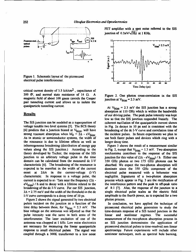
232 Ultrafast Electronics and Optoelectronics
FET amplifier with a spot noise referred to the SIS. -...... .... ........... .. ...... junction of O.2nV/4/ii at 1 KHz.
Fetwaw J2 VbiŽI Rd 4. X1:1Vbia; 2.3 mV
'DC 8 I
"2 -
Figure 1. Schematic layout of the picosecond 0
electrical pulse interferometer. "_-_o ____-_o . _________o_____-80 -60 -40 -X( 0 20 40 W0 N0
Time Delay (ps)
critical current density of 3.5 kA/cm2 , capacitance of200 iF, and normal state resistance of 14 fl. A Figure 2. One photon cross-correlation in the SISmagnetic field of about 100 gauss cancels the Cooper junction at Vbias = 2.3 mV.pair tunneling current and allows us to isolate thequasiparticle tunneling current. At Vbias = 2.3 mV the SIS junction has a strong
absorption at 110 GHz which is within the bandwidthResults of our driving pulse. The peak pulse intensity was kept
low so that the SIS junction responded linearly. TheThe SIS junction can be modeled as a superposition of coherent oscillation of the quasiparticle current shownvoltage tunable two level systems [51. The BCS theory in Fig. 2a decays in 10 ps and is consistent with the[61 predicts that a junction biased at Vbias, will have broadening of the dc I-V curve and correlation time ofstrong resonant absorption when hf0 = 2A - eVbias, the incident pulses. In future experiments we plan toAs in atomic or semiconductor systems, the width of use both faster pulses and devices which ring with athe resonance is due to lifetime effects as well as longer decay time.inhomogeneous broadening (distribution of energy gap Figure 3 shows the result of a measurement similarvalues along the SIS junction.) According to the to Fig. 2, except that Vbias = 1.3 mV. Two absorptiontheory developed by Tucker, the response of the SIS mechanisms contribute to the response of the SISjunction to an arbitrary voltage pulse in the time junction for this value of (2A - eVbias) / h. Either onedomain can be calculated from the measured dc I-V 350 GHz photon or two 175 GHz photons can becharacteristic [6]. The broadening of the resonance is absorbed. We expect the two-photon absorption willexpected to be manifest in the width of the current dominate since the 350 GHz component of theonset at 2A/e in the current-voltage (I-V) electrical pulse measured with a bolometer wascharacteristic. In response to a voltage pulse, the negligible. Signatures of a two-photon absorptioncurrent is expected to o!. !late near the frequency (2A - process which appear in Fig. 3 are the rectification ofeVbias) / h and to decay with a lifetime related to the the interference pattern and the peak to off-peak ratiobroadening of the dc I-V curve. For our SIS junction, of 8:1 171. Also, the response of the junction to a2A = 2.75 meV and the width of the threshold in the dc single electrical pulse scales as the electric fieldI-V curve corresponds to a decay time of 10 ps. amplitude to the fourth power, as is expected for a two
Figure 2 shows the signal generated by two electrical photon process.pulses incident on the junction as a function of the In conclusion, we have applied the technique oftime delay between them, for Vbias = 2.3 mV. The picosecond electrical pulse generation to study thebias voltage on the antennas was adjusted so that the time-domain response of a SIS tunnel junction in thepulse intensity was the same in both arms of the linear and nonlinear regimes. The successfulinterferometer. The laser excitation of one of the measurement of the two-photon absorption process inantennas was chopped at 1 kHz. Low noise electronics an SIS junction demonstrates the application ofare necessary for measuring the linear quasiparticle picosecond electrical pulses to time-resolved non-linearresponse to small electrical pulses. The signal was spectroscopy. Future experiments will include othercoupled through a 300K transformer to a low noise nonlinear techniques, such as spectral hole burning,
U rlftrr Electromcs and Opoelectromcs 233
1 , References
Vbias-=.3 mV
- [1] P. L. Richards and Q. Hu, Proc. IEEE 60, 1233,(1989).
f2] Q. Hu, C. A. Mears, P. L. Richards and F. L.Lloyd, Phys. Rev. Lett. 64 2945 (1990); A. H.
W 4 Worsham, N. G. Ugras, D. Winkler, D. E.2 Prober, N. R. Erickson, P. F. Goldsmith, Phys.
Rev. Lett. 67, 3034 (1991).0-t. [31 M. van Exter, D. Grischkowsky, IEEE Trans.
0 -6 -40 -20 0 20 40 60 so MTr 38, 1684 (1990).Time Delay (ps) [4] S.E. Ralph, D. Grischkowsky, App. Phys. Lett.
Figure 3. Two photon cross-correlation in the SIS 60, 1070 (1992); B.I.Greene, J.F. Federici, D.R.junction at Vbias = 1.3 mV. Dykaar, R.R. Jones, P.H. Bucksbaum, App.
Phys. Lett ý, 893 (1991).which may allow us to probe the mechanism which [51 Q. Hu, C.A. Mears, P.L. Richards, F.L. Lloyd,whicdensth e may aw cus e tof the mejunchanism whPhys. Rev. B 42 10250 (1990).broadens the dc I-V curve of the S15 junction. [61 J. R. Tucker, M.J. Feldman, Rev. Mod. Phys. 57,
Acknowledements 1055 (1985).
[71 J.-C. M. Diels, J. J. Fontaine, I. C. McMichael, F.
This work is supported by U.S. DOE under contract Simoni, Applied Optics 24. 1270 (1985).
DE-AC03-76SF00098.
Ultrafast Optical and Optoelectronic Response ofY-Ba-Cu-O
T. Gong, L. X. Zheng, Y. Kostoulas*, W. Xiong, W. Kula+,K. B. Ucer, Roman Sobolewski+, and P. M. Fauchet
Laboratory for Laser Energetics and Department of Electrical Engineering,University of Rochester, 250 East River Road,
Rochester, New York 14623-1299
Since the discovery of high-temperature superconductors selected from a white-light continuum. Time-resolved differential(HTS), there have been intensive investigations of their transient reflectivity (ARIR) measurements have been performed with aresponse under ultashort laser-pulse excitation. Recently, using temporal resolution of -100 fs on various YBCO films and atthe femtosecond pump-probe technique, Han et al. [1] observed a different temperatures.very fast (several picoseconds) optical response on YBa 2Cu30x In order to locate EF in the oxygen p-band of the Cu-O plane,(YBCO) in the superconducting state under weak excitation and we first performed 2-eV-pumplwhite-light-probe measurementsattributed it to the generation and recombination of quasi- on oxygen-rich YBCO (x Z 6.9, d - 200 un, Tc - 87 K) andparticles. As the ambient temperature drops below the oxygen-poor YBCO (x S 6.45, d - 200 nm, Tc - 0 K) at roomsuperconductor's critical temperature (Td), the transient temperature. We have observed [31 that for oxygen-rich YBCO,reflectivity signal abruptly changes both its sign and temporal ARIR is always positive in the frequency range of 1.91 to 2.25 eV;behavior--this striking behavior appears to be correlated to the in contrast, for oxygen-poor YBCO, ARIR is always negative inonset of superconductivity. However, the physical significance of the frequency range of 1.46 to 2.00 eV. Using the standardsuch an ultrafast response is still not clear, since the position of thermomodulation (Fermi smearing) model, we conclude usingthe Fermi level (EF) and the density of states near EF are not well the hole picture that EF must be at least 2.25 eV above theknown. Independently, a series of transient photovoltage Cu-d9/d10 band for YBCO with x z 6.9, but at most 1.45 eVmeasurements have also been performed on YBCO. Recent above the Cu-d9/dl 0 band for YBCO with x z 6.45. The largeexperimental work [21 demonstrated that for ultra-thin films the shift (>800 meV) of EF when the oxygen content decreases fromrelative magnitude of the nonthermal component was enhanced Z6.90 to :S6.45, can be explained by the drastic decrease of theand could be as fast as tens of picoseconds. The fact that the total charge density in the Cu-O planes.electrical response is at least one order of magnitude slower than In order to determine EF as a function of x, we havethe optical response suggests that more in-depth studies are performed similar measurements on several YBCO samples withnecessary in order to find the ultimate speed of optoelectronic different oxygen contents. These samples were obtained bydevices made of HTS. annealing high-quality superconducting films in controlled Ar-0 2-
In this paper, we present a series of ultrafast photoexcitation mixture atmospheres. Figure 1 shows the time-resolved ARMRmeasurements of YBCO. We focus our attention on detailed signal measured at 2 eV on the YBCO samples with five differentstudies of the transient optical response as a function of optical oxygen contents---estimated by measuring T,. From the signfrequency, oxygen content (x) and thickness (d) of the sample, reversal of the signal, when x approaches 6.8 (Tc - 60 K), weexcitation intensity (1p), and electric current (I). Preliminary conclude that EF lies -2 eV above the Cu-d9/d1 0 band forphotovoltage measurements, using the technique of photoinduced x - 6.8±0.05 (adopting the framework of the thermomodulationresistive autocorrelation, are also presented. These measurements model).address the question of the ultimate time resolution for the When the ambient temperature drops below Tc, the free-electrical response of YBCO under ultrafast optical excitation, carrier density of states in the superconductor is modifiedwhich has a direct impact on device applications, substantially. According to the BCS theory, in the
The transient optical response is measured using conventional superconducting state (i) electrons form boson-like Cooper pairs,pump-probe techniques with a copper-vapor laser amplified CPM which occupy a single energy level separated from EF by thesystem. The experimental arrangement allows us to change the superconducting energy gap A: while (ii) unpaired, excitedpump laser intensity for 2-eV photons by more than three orders electrons (quasi-particles) occupy a continuum of states startingof magnitude, as well as to use different probe wavelengths A above EF. Under optical illumination, the thermal equilibrium
OSA Prodeng•i UonUbr EfraroukmnadOpwelktroaicmx 1993, VoL 14 234Jqdeep Mhk ad U/w MIAr (o&)0 1993 Opticka Soc'ty ofAmerica
Ultrafast Electronics and Optoelectronics 235
between the superconducting condensate and quasi-particles isdisturbed (often very strongly), since photons with energies >>2Acan break Cooper pairs and create quasi-particles. The absorptionof a single 2-eV photon in YBCO creates, through the cascadingprocesses of carrier-carrier and carrier-phonon scattering, manyquasi-particles with energies widely distributed above 2A. Thus,even a relatively weak optical excitation leads to highlynonequilibrium transient Cooper pair/quasi-particle distributions.
0-content
;e6.90
S&6.81
(d)
1 6.60
s-6.45 69 4-ps -z13WZ411 Delay
Figure 2. Normalized ARIR measured at T < T, on opticallythick and thin YBCO at 2 eV and different excitation intensity:- -ps delay • (a)d-280nm, T=25K, andlp- lIJ/cm2;(b) d-80nm, T=25 K, and IT ~- lJl/cn2; (c) d - 200 nm, T = 12 K, and lp -
Z1516 20 Iil/cm2; and (d) d - 200 nm, T = 12 K, and lp - 100 pJ/cm2.Figure 1. Normalized ARMR measured on the YBCO samples there are two problems associated with the above picture: (i) Thewith different oxygen contents at room temperature using a 2-eV detailed band structure, in particular around EF, is neglected;probe photon energy. The measured critical temperature and (ii) One assumes that the measured ARMR signal is dominated byestimated oxygen content of each sample is displayed. Aa (the change of absorption coefficient). The first problem was
Figure 2(a) shows ARMR at 2 eV measured at T = 25 K on an recently revealed to be important by systematic studies onoptically thick superconducting sample (d - 280 nm, Tc - 87 K) Pr-doped YBCO [51, as well as studies on the specific-heatwhen a weak excitation (IP - I piJ/cm2 ) is used. The negative discontinuity on YBCO at Tc 16]. The second assumption,ARMR, followed by a fast (several picoseconds) recovery, is very however, contradicts the fact that the sign of the transientsimilar to the literature results obtained on optically thick (from transmission (AT/T) remains the same (negative) with onset of250-nm- to 500-nm-thick) samples [1,4,5], and has been attributed superconductivity (7,8]. Figure 2(b) shows a positive AR/R withto the generation and recombination of quasi-particles [1] and/or temporal response similar to that exhibited in Fig. 2(a), obtainedthe relaxation of the superconducting order parameter [41. On the on the optically thin (d - 80 nm Tc - 84 K) sample. Theseother hand, the temperature dependence of the relaxation time experimental evidences appear to suggest that such aobtained from ARIR appears to depend on sample's quality and "nonbolometric" response is caused by An (the change ofexcitation ititensity 11,4,51. If one combines the framework of the refractive index) instead of Aa. Thus, the sign change between thethermomodulation model with the superconductor's two-fluid optically thin and thick films is due to the thin-film effect. Themodel, the observed magnitude of the ARIR signal appeared to analysis [3) also shows that a simple two-fluid model cannotagree with the simple estimation presented in Ref. 1. A possible satisfactorily explain the behavior of An. One possibility is toexplanation of the sign reversal of the signal with onset of attribute such a peculiar behavior to the optical response ofsuperconductivity is as follows: breaking of Cooper pairs and YBCO in a nonequilibrium intermediate state, which can existgeneration of quasi-particles cause a reduction of A, which under the low excitation. The intermediate state, which was firstdecreases the absorption below EF-A, thus at 2 eV. However, observed by Sai-Halasz et al. 191 in metallic superconductors, is
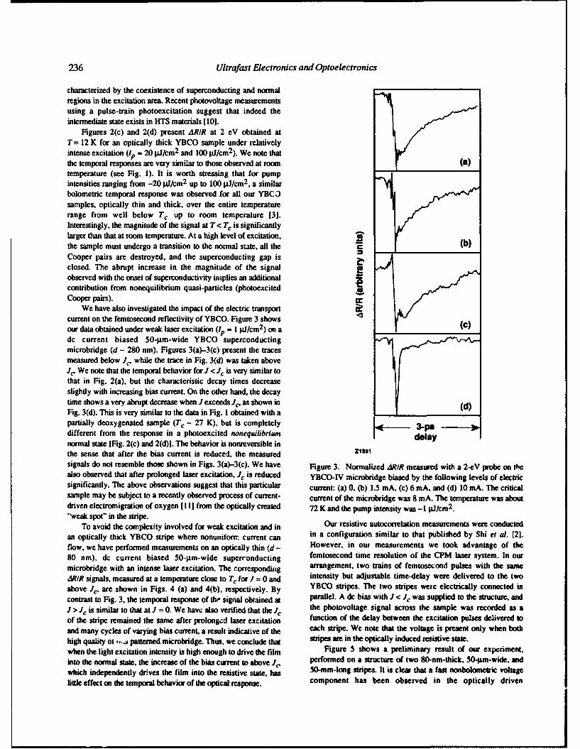
236 Ultrafast Electronics and Optoelectronics
characterized by the coexistence of superconducting and normalregions in the excitation area. Recent photovoltage measurementsusing a pulse-train photoexcitation suggest that indeed theintermediate state exists in HTS materials [10].
Figures 2(c) and 2(d) present ARIR at 2 eV obtained atT= 12 K for an optically thick YBCO sample under relativelyintense excitation (lp - 20 p.J/cm 2 and 100 p/cm2 ). We note thatthe temporal responses are very similar to those observed at roomtemperature (see Fig. 1). It is worth stressing that for pumpintensities ranging from -20 pj/cm2 up to 100 p.1/cm 2 , a similarbolometric temporal response was observed for all our YBC3)samples, optically thin and thick, over the entire temperaturerange from well below T, up to room temperature [3].Interestingly, the magnitude of the signal at T < T, is significantlylarger than that at room temperature. At a high level of excitation, i(the sample must undergo a transition to the normal state, all the -- (b)
Cooper pairs are destroyed, and the superconducting gap is Z
closed. The abrupt increase in the magnitude of the signalobserved with the onset of superconductivity implies an additionalcontribution from nonequilibrium quasi-particles (photoexcited aCooper pairs).
We have also investigated the impact of the electric transportcurrent on the femtosecond reflectivity of YBCO. Figure 3 showsour data obtained under weak laser excitation (Ip_ -I pJ/cm2) on adc current biased 50-p1m-wide YBCO superconductingmicrobridge (d- 280 nm). Figures 3(a)-3(c) present the tracesmeasured below J, while the trace in Fig. 3(d) was taken aboveJ,- We note that the temporal behavior for J < Jc is very similar tothat in Fig. 2(a), but the characteristic decay times decreaseslightly with increasing bias current. On the other hand, the decaytime shows a very abrupt decrease when J exceeds J, as shown in (d)Fig. 3(d). This is very similar to the data in Fig. 1 obtained with apartially deoxygenated sample (Tc - 27 K), but is completely 3.pdifferent from the response in a photoexcited nonequilibrium delaynormal state [Fig. 2(c) and 2(d)]. The behavior is nonreversible inthe sense that after the bias current is reduced, the measured Z1351signals do not resemble those shown in Figs. 3(a)-3(c). We have Figure 3. Normalized ARIR measured with a 2-eV probe on thealso observed that after prolonged laser excitation, Jc is reduced YBCO-IV microbridge biased by the following levels of electricsignificantly. The above observations suggest that this particular current: (a) 0. (b) 1.5 mA, (c) 6 mA, and (d) 10 mA. The criticalsample may be subject to a recently observed process of current- current of the microbridge was 8 mA. The temperature was aboutdriven electromigration of oxygen [I II from the optically created 72 K and the pump intensity was -1 I p/cm2 ."weak spot" in the stripe.
To avoid the complexity involved for weak excitation and in Our resistive autocorrelation measurements were conductedan optically thick YBCO stripe where nonuniform current can in a configuration similar to that published by Shi et al. [21.flow, we have performed measurements on an optically thin (d - However, in our measurements we took advantage of the80 nm), dc current biased 50-ptm-wide superconducting femtosecond time resolution of the CPM laser system. In ourmicrobridge with an intense laser excitation. The corresponding arrangement, two trains of femtosecond pulses with the sameARIR signals, measured at a temperature close to T, for J = 0 and intensity but adjustable time-delay were delivered to the twoabove J, are shown in Figs. 4 (a) and 4(b), respectively. By YBCO stripes. The two stripes were electrically connected incontrast to Fig. 3, the temporal response of the signal obtained at parallel. A dc bias with J < Jc was supplied to the structum andJ > Jc is similar to that at J = 0. We have also verified that the J, the photovoltage signal across the sample was recorded as aof the stripe remained the same after prolonged laser excitation function of the delay between the excitation pulses delivered toand many cycles of varying bias current, a result indicative of the each stripe. We note that the voltage is present only when bothhigh quality o ,,,.s patterned microbuidge. Thus. we conclude that stripes are in the optically induced resistive state.when the light excitation intensity is high enough to drive the film Figure 5 shows a preliminary result of our experiment,into the normal state, the increase of the bias current to above J) performed on a structure of two 80-nm-thick, 50-ptm-wide, andwhich independently drives the film into the resistive state, has 50-mm-long stripes. It is clear that a fast nonbolometric voltagelittle effect on the temporal behavior of the optical response. component has been observed in the optically driven
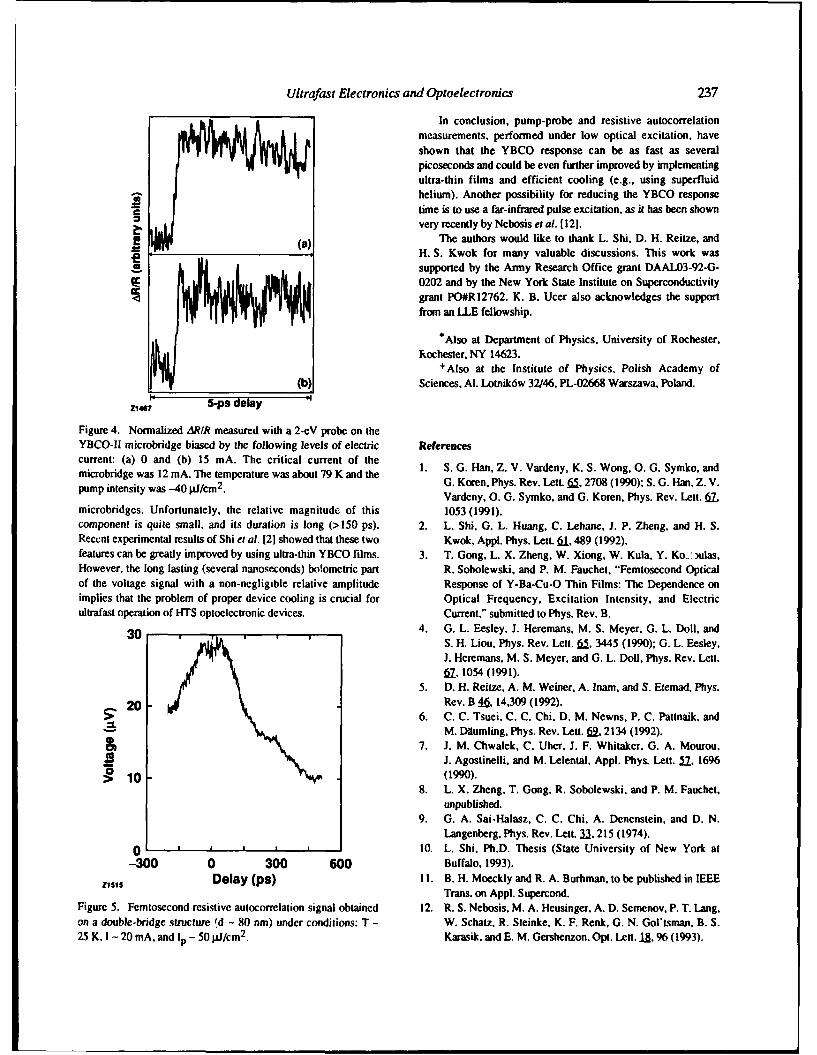
Ultrafast Electronics and Optoelectronics 237
In conclusion, pump-probe and resistive autocorrelationmeasurements, performed under low optical excitation, haveshown that the YBCO response can be as fast as severalpicoseconds and could be even further improved by implementingultra-thin films and efficient cooling (e.g., using superfluid
T helium). Another possibility for reducing the YBCO responsetime is to use a far-infrared pulse excitation, as it has been shownvery recently by Nebosis et al. [121.
The authors would like to thank L. Shi. D. H. Reitze, and= -H. S. Kwok for many valuable discussions. This work was4 supported by the Army Research Office grant DAAL03-92-G-
0202 and by the New York State Institute on Superconductivitygrant PO#RI2762. K. B. Ucer also acknowledges the supportfrom an LLE fellowship.
'Also at Department of Physics, University of Rochester,Rochester, NY 14623.
+Also at the Institute of Physics, Polish Academy of(b) Sciences, Al. Lotnik6w 32/46, PL-02668 Warszawa, Poland.
Z17 5-ps delay
Figure 4. Normalized ARIR measured with a 2-eV probe on theYBCO-11 microbridge biased by the following levels of electric Referencescurrent: (a) 0 and (b) 15 mA. The critical current of the 1. S. G. Han, Z. V. Vardeny, K. S. Wong, 0. G. Symko, andmicrobridge was 12 mA. The temperature was about 79 K and thepump intensity was --40 IJ/crn2. G. Koren, Phys. Rev. Lett. 65, 2708 (1990); S. G. Hanl, Z. V.
Vardeny, 0. G. Symko, and G. Koren, Phys. Rev. Lett. 67,
microbridges. Unfortunately, the relative magnitude of this 1053 (1991).component is quite small, and its duration is long (>150 ps). 2. L. Shi. G. L. Huang. C. Lehane, J. P. Zheng, and H. S.Recent experimental results of Shi et al. [2] showed that these two Kwok, Appl. Phys. Lett 61, 489 (1992).features can be greatly improved by using ultra-thin YBCO films. 3. T. Gong, L. X. Zheng, W. Xiong, W. Kula, Y. Ko- ,ulas,However. the long lasting (several nanoseconds) bolometric part R. Sobolewski, and P. M. Fauchet, "Femtosecond Opticalof the voltage signal with a non-negligible relative amplitude Response of Y-Ba-Cu-O Thin Films: The Dependence onimplies that the problem of proper device cooling is crucial for Optical Frequency, Excitation Intensity, and Electricultrafast operation of HTS optoelectronic devices. Current," submitted to Phys. Rev. B.
30 4. G. L. Eesley, J. Heremans, M. S. Meyer, G. L. Doll, andS. H. Liou, Phys. Rev. Lett. 65, 3445 (1990); G. L. Eesley,J. Heremans, M. S. Meyer, and G. L. Doll. Phys. Rev. Lett.6, 1054 (1991).
5. D. H. Reitze, A. M. Weiner, A. lnam, and S. Etemad, Phys.
20 Rev. B 4M, 14,309 (1992).6. C. C. Tsuei, C. C. Chi, D. M. Newns, P. C. Pattnaik, and
M. D~Iumling, Phys. Rev. Lett. 69, 2134 (1992).S7. J. M. Chwalek, C. Uher. J. F. Whitaker, G. A. Mourou.
J. Agostinelli. and M. Lelental, Appl. Phys. Lett. 51, 16960i (1990).> 10(lX.
8. L. X. Zheng, T. Gong. R. Sobolewski, and P. M. Fauchet,unpublished.
9. G. A. Sai-Halasz. C. C. Chi, A. Denenstein, and D. N.Langenberg, Phys. Rev. Lett. 33,215 (1974).
0 * * * * , 10. L. Shi. Ph.D. Thesis (State University of New York at
-300 0 300 600 Buffalo, 1993).
Z1515 Delay (ps) 11. B. H. Moeckly and R. A. Burhman, to be published in IEEETrans. on Appl. Supercond.
Figure 5. Femtosecond resistive autocorrelation signal obtained 12. R. S. Nebosis. M. A. Heusinger. A. D. Semenov, P. T. Lang.on a double-bridge structure 'd - 80 nm) under conditions: T - W. Schatz, R. Steinke, K. F. Renk, G. N. Gol'isman. B. S.25 K. I - 20 mA, and lp - 50 pj/cm 2 . Karasik, and E. M. Gershenzon, Opt. Lett. la, 96 (1993).
Terahertz Spectroscopy of Superconducting Thin FilmBao.Ko.4BiO3
Yongqian Liu and John F. WhitakerCenterfor Ultrafast Optical Science, University of Michigan, 2200 Bonisteel Blvd,
Ann Arbor, Michigan 48109-2099
Christine E. Platt
University of Illinois at Urbana Champaign, Science and Technology Center for Superconductivity,320 Materials Research Laboratory, Urbana, Illinois 61801
Abstract Terahertz-radiation, time-domain spectroscopy,with its high sensitivity and wide bandwidth, has
The complex conductivity of a Ba0.6K0 .4BiO 3 thin- become a powerful tool for studying the electronicfilm superconductor has been measured using terahertz- properties of materials in a region of theradiation spectroscopy. A BCS-like energy gap and a electromagnetic spectrum that is not easily accessiblepeak in the real part of the conductivity have been [3-6]. With this technique, both phase and amplitudedirectly obtained without the need for Kramers-Kronig information are obtained directly from a measurement,analysis. so that the real and imaginary parts of, for instance, the
index of refraction, permittivity, or conductivity of asample under study can be determined without using
Introduction Kramers-Kronig analysis. For example, recent terahertzbandwidth measurements have determined the complex
Studies of the properties of superconducting thin films conductivity of the high-Tc superconductor,in the millimeter and submillimeter-wave range are of YBa2Cu307.x [4,51. These results are significant ingreat interest for both the physical insight they lend their demonstration that the material exhibits behaviorinto the behavior of materials and the relevant that may not be attributed to BCS theory.technological information they provide regarding The cubic, copper-free oxide Ba 0 .6K0 .4BiO 3applications. Scientifically, for example, measurements (BKBO) stands out as a superconductor with a moderateof the frequency and temperature dependences of the critical temperature between that of conventional BCScomplex conductivity of low-critical-temperature (Tc) superconductors and high-Tc superconducting coppersuperconductors in this regime have played a crucial role oxides. Due to its long coherence length and itsin understanding the fundamental nature of the quasiparticle and Josephson tunneling properties, BKBOinteraction responsible for conventional has been considered as a possible material system in asuperconductivity [1,2]. In addition, they have provided new family of superconducting circuits [7].quantitative support for the BCS theory in these Furthermore, there is clear evidence of an energy gap insuperconductors. Technologically, on the other hand, BKBO [8], and other indications also suggest thatstudies of superconducting behavior at frequencies BKBO is an ordinary electron-phonon-coupled BCScorresponding to energies below the gap energy are superconductor [9]. On the other hand, since it has alsoimportant because of the potential use of high-Tc been reported that BKBO shares many characteristicssuperconductors in passive microwave devices for high- with the cuprate high-Tc superconductors, its furtherfrequency electronics. study should enhance the understanding of both material
OSA PAoceahrms o w Ubr* em o aec nd 0 Iro•kcOp dm 1993, Vol 14 238Jqpdep Vlia aid UmeaA MdMm (edt)* 1993 Op"k Sodety ceAimad
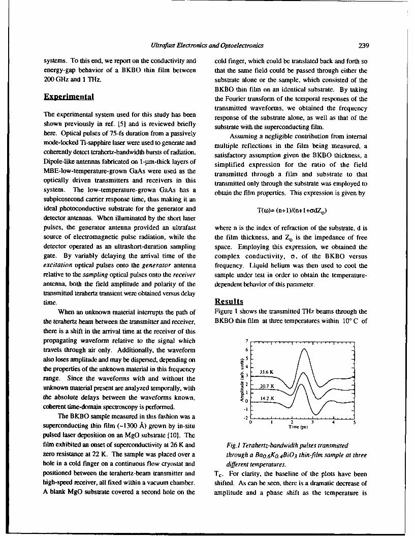
Ultrafa/s Electronics and Optoelectronics 239
systems. To this end, we report on the conductivity and cold finger, which could be translated back and forth soenergy-gap behavior of a BKBO thin film between that the same field could be passed through either the200 GHz and I THz. substrate alone or the sample, which consisted of the
BKBO thin film on an identical substrate. By takingExpeimental the Fourier transform of the temporal responses of the
transmitted waveforms, we obtained the frequencyThe experimental system used for this study has been response of the substrate alone, as well as that of theshown previously in ref. [51 and is reviewed briefly substrate with the superconducting film.here. Optical pulses of 75-fs duration from a passively Assuming a negligible contribution from internalmode-locked Ti-sapphire laser were used to generate and multiple reflections in the film being measured, acoherently detect terahertz-bandwidth bursts of radiation, satisfactory assumption given the BKBO thickness, aDipole-like antennas fabricated on 1-p1m-thick layers of simplified expression for the ratio of the fieldMBE-low-temperature-grown GaAs were used as the transmitted through a film and substrate to thatoptically driven transmitters and receivers in this transmitted only through the substrate was employed tosystem. The low-temperature-grown GaAs has a obtain the film properties. This expression is given bysubpicosecond carrier response time, thus making it anideal photoconductive substrate for the generator and T((o)= (n+l)/(n+l+odZo)detector antennas. When illuminated by the short laserpulses, the generator antenna provided an ultrafast where n is the index of refraction of the substrate, d issource of electromagnetic pulse radiation, while the the film thickness, and Zo is the impedance of freedetector operated as an ultrashort-duration sampling space. Employing this expression, we obtained thegate. By variably delaying the arrival time of the complex conductivity, a, of the BKBO versusexcitation optical pulses onto the generator antenna frequency. Liquid helium was then used to cool therelative to the sampling optical pulses onto the receiver sample under test in order to obtain the temperature-antenna, both the field amplitude and polarity of the dependent behavior of this parameter.transmitted terahertz transient were obtained versus delaytime. Results
When an unknown material interrupts the path of Figure 1 shows the transmitted THz beams through thethe terahertz beam between the transmitter and receiver, BKBO thin film at three temperatures within 100 C ofthere is a shift in the arrival time at the receiver of thispropagating waveform relative to the signal whichtravels through air only. Additionally, the waveform 6
also loses amplitude and may be dispersed, depending on -5 -
the properties of the unknown material in this frequency 3 4 3.K
range. Since the waveforms with and without the 3unknown material present are analyzed temporally, with ,2the absolute delays between the waveforms known, 142 <.coherent time-domain spectroscopy is performed.
The BKBO sample measured in this fashion was a -2 "..0 1 2 3 4superconducting thin film (-1300 A) grown by in-situ Time (p4)
pulsed laser deposition on an MgO substrate [101. Thefilm exhibited an onset of superconductivity at 26 K and Fig. ) Terahertz-bandwidth pulses transmittedzero resistance at 22 K. The sample was placed over a through a Ba 0 o6 K. 4 Bi0 3 thin-film sample at threehole in a cold finger on a continuous flow cryostat and different temperatures.positioned between the terahertz-beam transmitter and Tc. For clarity, the baseline of the plots have beenhigh-speed receiver, all fixed within a vacuum chamber. shifted. As can be seen, there is a dramatic decrease ofA blank MgO substrate covered a second hole on the amplitude and a phase shift as the temperature is
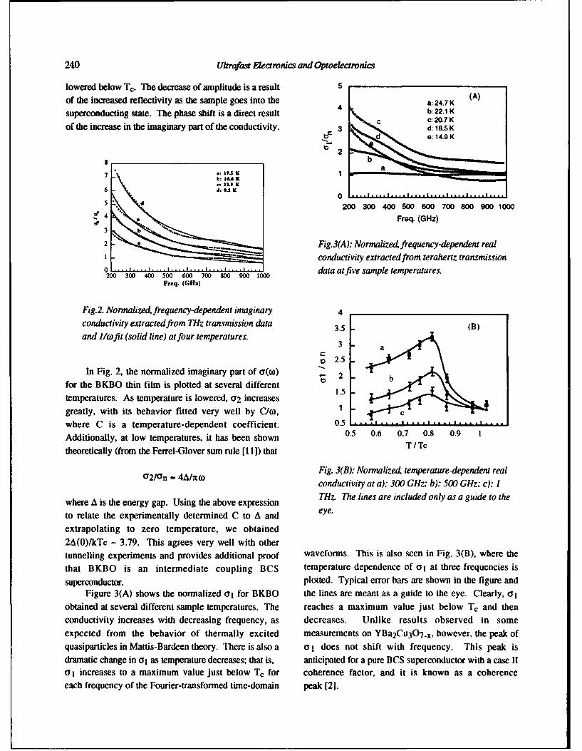
240 Ultrafasr Electronics and Optoelectronics
lowered below Tc. The decrease of amplitude is a result 5of the increased reflectivity as the sample goes into the a: 24.7K (A)
superconducting state. The phase shift is a direct result b: 22.1 KC c: 20.7 K
of the increase in the imaginary part of the conductivity. 3 d: 18.5Kt: e: 14.9 K
028
7 1. K
•.€ 1 .td ' 9.2 K0
200 300 400 500 600 700 800 900 10004. Freq. (GHz)3 b L•
2 Fig.3(A): Normalized, frequency-dependent realconductivity extracted from terahertz transmission
" .... data at five sample temperatures.200 300 400 500 600 700 800 900 1000
Freq. (GHz)
Fig.2. Normalized, frequency-dependent imaginary 4
conductivity extracted from THz transmission data 3.5 (B)
and 1/rfit (solid line) at four temperatures.3
c 2.5
In Fig. 2, the normalized imaginary part of o(co) 2for the BKBO thin film is plotted at several different 1
temperatures. As temperature is lowered, 02 increases 1.5greatly, with its behavior fitted very well by C/co, 1where C is a temperature-dependent coefficient. 0.5Additionally, at low temperatures, it has been shown 0.5 0.6 0.7 0.8 0.9 1
theoretically (from the Ferrel-Glover sum rule [11]) that T/Tc
(72/cyn = 4A/n3 Fig. 3(B): Normalized, temperature-dependent realconductivity at a): 300 GHz; b): 500 GHz; c): 1THz. The lines are included only as a guide to the
where A is the energy gap. Using the above expression
to relate the experimentally determined C to A and eye.
extrapolating to zero temperature, we obtained2A(0)/kTc - 3.79. This agrees very well with othertunnelling experiments and provides additional proof waveforms. This is also seen in Fig. 3(B), where the
that BKBO is an intermediate coupling BCS temperature dependence of o0 at three frequencies is
superconductor. plotted. Typical error bars are shown in the figure andFigure 3(A) shows the normalized al for BKBO the lines are meant as a guide to the eye. Clearly, 01
obtained at several different sample temperatures. The reaches a maximum value just below T. and thenconductivity increases with decreasing frequency, as decreases. Unlike results observed in someexpected from the behavior of thermally excited measurements on YBa 2 Cu307.x, however, the peak ofquasiparticles in Mattis-Bardeen theory. There is also a 1 I does not shift with frequency. This peak isdramatic change in aI as temperature decreases; that is, anticipated for a pure BCS superconductor with a case II0 I increases to a maximum value just below Tc for coherence factor, and it is known as a coherenceeach frequency of the Fourier-transformed time-domain peak [2).
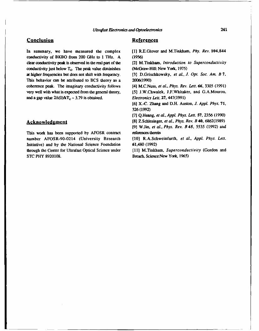
Uln9'ast Eectronics and Oproelectronics 241
Conclusion References
In summary, we have measured the complex [1] R.E.Glover and M.Tinkham, Phy. Rev. 104,844
conductivity of BKBO from 200 GHz to 1 THz. A (1956)clear conductivity peak is observed in the real part of the [2] M.Tinkbam, Introduction to Superconductivity
conductivity just below Tc. The peak value diminishes (McGraw-Hill: New York, 1975)
at higher frequencies but does not shift with frequency. [3] D.Grischkowsky, et al., J. Opt. Soc. Am. B 7,This behavior can be attributed to BCS theory as a 2006(1990)coherence peak. The imaginary conductivity follows [41 M.C.Nuss, et at., Phys. Rev. Lett. 66, 3305 (1991)very well with what is expected from the general theory, (5] J.W.Chwalek, J.F.Whitaker, and G.A.Mourou,and a gap value 2A(0)/kT. - 3.79 is obtained. Electronics Lett. 27, 447(1991)
[6] X.-C. Zhang and D.H. Auston, J. Appl. Phys. 71,326(1992)[7] Q.Huang, et al., Appl. Phys. Lett. 57, 2356 (1990)
Acknowledgment [8] Z.Schlesinger, et al., Phys. Rev. B 40, 6862(1989)
[9] W.Jin, et al., Phys. Rev. B 45, 5535 (1992) and
This work has been supported by AFOSR contract references thereinnumber AFOSR-90-0214 (University Research [10] R.A.Schweinfurth, et al., AppL. Phys. Lett.
Initiative) and by the National Science Foundation 61,480 (1992)through the Center for Ultrafast Optical Science under [11] M.Tinkham, Superconductivity (Gordon and
STC PHY 8920108. Breach, Science:New York, 1965)
Ultrafast Quasiparticles Dynamics in High-TemperatureSuperconductors
W. Albrecht, Th. Kuse, K. Leo, and H. Kurz
Insrwiufi rHalbleitertechnik, RWTH Aachen, Sommerfedt&rasse 24,W-51OOAachein, Germany
Abstract to study QP dynamics in the time domain. Experimentswhich probe the electrical response after photoexcitation
We report about a detailed study of the dynamics of laser- with an ultrashort laser pulse have been used to study theexcited quasiparticles in "YBa2CU3O7-thin films. We QP dynamics for both LTS [4-6] and HTS [7,8], with apropose a model of the low-temperature response which time-resolution presently limited to about 10ps. Recently,links the reflectivity transients at low temperature to the femtosecond transmission and reflectivity techniques havegeneration and recombination behavior of quasiparticles. been employed to study the optical response of HTS withThe quasiparticle recombination rate is determined by higher time resolution [9]. Measurements at lowcomparison with a model of the quasiparticle dynamics temperatures have addressed the non-bolometric responsebased on the extended Rothwarf-Taylor equations. The due to photogenerated quasiparticles and indicate veryrecombination rates in the high-Tc materials are close to short QP recombination times [10-12]. However, thethe rates of conventional superconductors. mechanism of the low-temperature optical response and its
relation to the QP dynamics were not clarified [10,121.
IntroductionWe here report a systematic study of quasiparticle
Most of the studies of superconductivity have addressed recombination times in YBa2Cu3O7. We obtain the QPthe regime close to thermal and electronic equilibrium, dynamics from transient reflectivity changes for differenttheregme los tothemalandeletroic quiibrum. lattice temperatures and laser fluenees. Below T., weThe non-equilibrium properties of superconductors are lattice a and lase fluinces w ca weboth important for applications and for the basic observe a sign change of the optical signals which can beunderstanding of superconductivity [1-31. The relaxation well explained by the gap reduction due to the non-and recombination dynamics of Quasiparticles (QP), i.e., equilibrium QP. The experimental results are comparedCoopers pairs excited above the superconducting gap are with a detailed model of the QP dynamics based on theof particular importance for the properties of Rothwarf-Taylor equations (RTE), extended for ultrashortsuperconducting electronic devices. For conventional excitation and subsequent cascade generation of the QP.superconductors (LTS), extensive studies of the generation We deduce from data a recombination coefficient F =
and recombination dynamics of QP have been performed 4x10" cm~s-', similar to the rates of conventional(see Ref. 3). superconductors.The discovery of high-temperature superconductors (HTS)has renewed the interest in the physics of nonequilibrium Experimental Resultssuperconductivity and its relations to device applications.
The experiments are performed with 50 fs laser pulsesA number of experimental techniques have been applied from a colliding pulse mode locked laser (CPM). The
OSA heA'Wa on Ulut EWeco=v 4OCode,, jc^ 1993, VoL 14 242Jqdup 5d amd •Mid MoiAd. fk)o 1993 Opdeml Sodiy q'AniamU
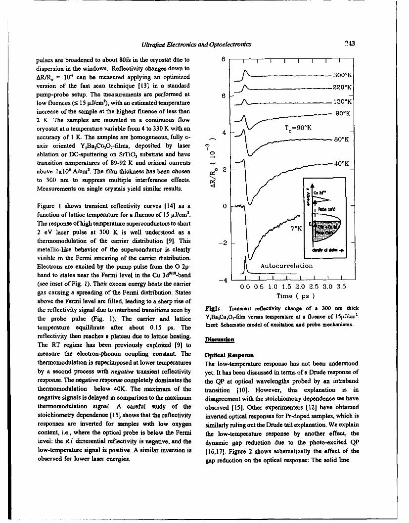
Ultrafast Electronics and Optoelectronics 243
pulses are broadened to about 80fs in the cryostat due to 8[dispersion in the windows. Reflectivity changes down toAR/Ro = 10.7 can be measured applying an optimized 3000 K
version of the fast scan technique [131 in a standard 220°Kpump-probe setup. The measurements are performed at 6low fluences (5 15 pJ/cm2), with an estimated temperature J- 130-K
increase of the sample at the highest fluence of less than 90 0 K2 K. The samples are mounted in a continuous flowcryostat at a temperature variable from 4 to 330 K with an 4 - -AZ Te=90°Kaccuracy of 1 K. The samples are homogeneous, fully c- 800 Kaxis oriented YBa2Cu 3O7-films, deposited by laser c'
ablation or DC-sputtering on SrTiO3 substrate and have 0-)
transition temperatures of 89-92 K and critical currents 40--above lx 106 A/cm2 . The film thickness has been chosen 0 2
to 300 nm to suppress multiple interference effects.Measurements on single crystals yield similar results.
Figure 1 shows transient reflectivity curves [14] as a 0function of lattice temperature for a fluence of 15 PJ/cm2 .The response of high temperature superconductors to short2 eV laser pulse at 300 K is well understood as athermomodulation of the carrier distribution [9]. This -2metallic-like behavior of the superconductor is clearly d a -0visible in the Fermi smearing of the carrier distribution.Electrons are excited by the pump pulse from the 0 2p- Autocorrelationband to states near the Fermi level in the Cu 3dWl,-band(see inset of Fig. 1). Their excess energy heats the carrier 0.0 0.5 1.0 1.5 2.0 2.5 3.0 3.5
gas causing a spreading of the Fermi distribution. States Time ( ps )above the Fermi level are filled, leading to a sharp rise ofthe reflectivity signal due to interband transitions seen by Figl: Transient reflectivity change of a 300 nm thick
the probe pulse (Fig. 1). The carrier and lattice YIBaCu3Orfilm versus temperature at a fluence of 15piJ/cm 2.
temperature equilibrate after about 0.15 ps. The Inset: Schematic model of excitation and probe mechanisms.
reflectivity then reaches a plateau due to lattice heating. DiscussionThe RT regime has been previously exploited [9] tomeasure the electron-phonon coupling constant. The Opfleal Responsethermomodulation is superimposed at lower temperatures The low-temperature response has not been understoodby a second process with negative transient reflectivity yet: It has been discussed in terms of a Drude response ofresponse. The negative response completely dominates the the QP at optical wavelengths probed by an intrabandthermomodulation below 40K. The maximum of the transition [10]. However, this explanation is innegative signals is delayed in comparison to the maximum disagreement with the stoichiometry dependence we havethermomodulation signal. A careful study of the obsfrved [151. Other experimenters [121 have obtainedstoichiometry dependence [ 151 shows that the reflectivity inverted optical responses for Pr-doped samples, which isresponses are inverted for samples with low oxygen similarly ruling out the Drude tail explanation. We explaincontent, i.e., where the optical probe is below the Fermi the low-temperature response by another effect, theievei: the R i ditterential reflectivity is negative, and the dynamic gap reduction due to the photo-excited QPlow-temperature signal is positive. A similar inversion is [16,17]. Figure 2 shows schematically the effect of theobserved for lower laser energies. gap reduction on the optical response: The solid line
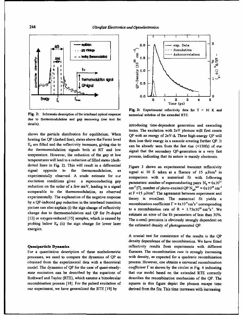
244 Ultrafast Electronics and Optoelectronics
I1I _T _ I
2.0 exp. Data 3detil),inrod g -d n gSimulation
t wiAutocorrelation w-~f (wW"a1.5
'I hI
hetnoteQ (dahe ine) 1ttsaoete-rilvl te oeter nryi acd raigfrhrQ.
E t oolt ignMlKsb oth a s"RTa
temperatue. H , te r ctio
- - ,.. -0.0 1 0UQV0 1 2 3 .4 5
Time (ps)
Fig. 3: Experimental reflectivity data for T to10 K andFig. 2: Schematic description of the interband optical response numerical solution of the extended RTE.due to thermomodulation and gap natrowing (see text fordetails), introducing time-dependent generation and cascading
terms. The excitation with 2eV photons will first createshows the particle distribution for equilibrium. When QP with an energy of 2eV-A. These high-energy QP willheating the QP (dashed line), states above the Fermi level then lose their energy in a cascade creating further QP. ItE, are filled and the reflectivity increases, giving rise to can be already seen from the fast rise (<1t fs) of ourthe thermomodulation signals both at RT and low signal that the secondary QP-generation is a very fasttemperature. However, the reduction of the gap at low process, indicating that its nature is mainly electronic.temperatures will lead to a reduction of filled states (dash-dotted lines in Fig. 2). This will result in a differential Figure 3 shows an experimental transient reflectivitysignal opposite to the thermomodulation, as signal at 10 K taken at a fluence of 15 thnJ/cm iexperimentally observed. A crude estimate for o Th comparison with a numerical fit with followingexcitation conditions gives a superconducting gap parameters: number of superconducting pairs N. = 6x 10²¹reduction on the order of a few meV, leading to a signal cm-' [71, number of photo-excited QP N .OLv = 6x IO's cm'comparable to the thermomodulation, as observed at F = 15 pJ/cm2 . The agreement between experiment andexperimentally. The explanation of the negative response theory is excellent. The numerical fit yields aby a QP-induced gap reduction in the interband transition recombination coefficient oF= 4x 1eo0 incs' correspondingpicture can also explain (i) the sign change of reflectivity to a recombination rate of R = 1 n.75x 10i2 cmrsi. Wechange due to thermomodulation and QP for Pr-doped estimate an error of the fit parameters of less than 30%.[12] or oxygen-reduced [15] samples, which is caused by The overall precision is obviously strongly dependent onprobing below E, (ii) the sign change for lower laser the estimated density of photogenerated QP.energies.
A crucial test for consistence of the results is the QPdensity dependence of the recombination. We have fitted
Quasiparticle Dynamics reflectivity results from experiments with differentFor a quantitative description of these nonbolometric fluences. The recombination rate is strongly increasingprocesses, we need to compare the dynamics of QP as with density, as expected for a quadratic recombinationobtained from the experimental data with a theoretical process. However, one obtains a universal recombinationmodel. The dynamics of QP for the case of quasi-steady- coefficient r as shown by the circles in Fig. 4 indicatingstate excitation can be described by the equations of that our model based on the extended RTE correctlyRothwarf and Taylor (RTE), which assume a bimolecular describes the recombination mechanism of the QP. Therecombination process [18]. For the pulsed excitation of squares in this figure depict the phonon escape timeour experiment, we have generalized the RTE [ 191 by derived from the fits. This time increases with increasing
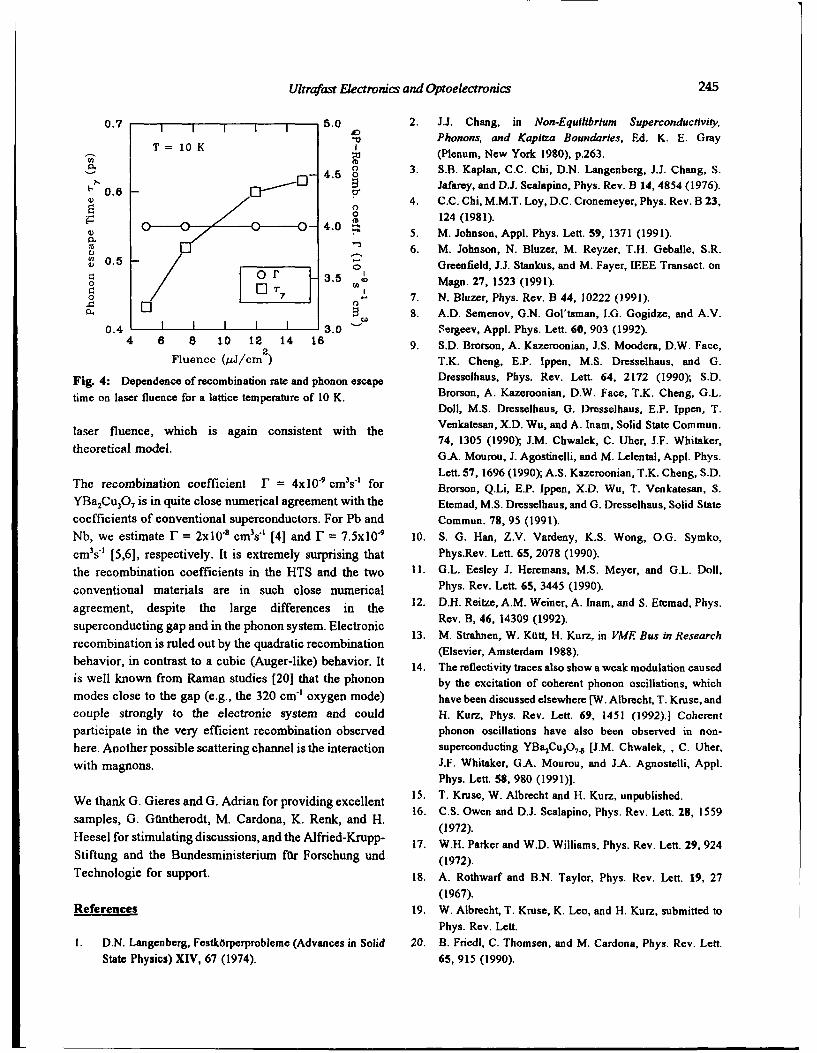
Ultrafast Electronics and Optoelectronics 245
0.7 1 . o2. i.J. Chang, in Non-Equilibrium Superconductivity.
T 10 K aPhonons, and Kapitza Boundaries, Ed. K. E. GrayT=W, (Plenum, New York 1980), p.26 3 .
4. 3. S.B. Kaplan, C.C. Chi, D.N. Langenberg, J.J. Chang, S.0.6.El- Jafarey, and D.J. Scalapino, Phys. Rev. B 14, 4854 (1976).
4. C.C. Chi, M.M.T. Loy, D.C. Cronemeyer, Phys. Rev. B 23,0
4. 12(1981).4. 5. M.Johnson, Appl. Phy:. Lett. 59, 1371 (1991). SR
S0.5o Greenfield, J.J. Stankus, and M. Fayer, IEEE Transact. on
o0~r Maga. 27, 1523 (1991).0o7 N. Bluzer, Phys. Rev. B 44, 10222 (1991).a. 8. A.D. Semenov, G.N. GoI'tsman, I.G. Gogidze, and A.V.
0.4 - 3.0 S.ergeev, AppI. Phys. Left. 60, 903 (1992).4 6 8 10 12 214 16 9. S.D. Brorson, A. Kazeroonian, J.S. Moodera, D.W. Face,
Fluence (p.J/cm ) T.K. Cheng, E.P. Ippen, M.S. Dresselbaus, and G.
Fig. 4: Dependence of recombination rate and phonon escape Dresseihaus, Phys. Rev. Lett. 64, 2172 (1990); S.D.
time on laser fluence for a lattice temperature of 10 K. Brorson, A. Kazeroonian, D.W. Face, T.K. Cheng, G.L.Doll, M.S. Dresselhaus, G. Dresselhaus, E.P. Ippen, T.
laser fluence, which is again consistent with the Venkatesan, X.D. Wu, and A. aina, Solid State Commun.
theoretical model. 74, 1305 (1990); J.M. Chwalek, C. Uher, J.F. Whitaker,GA. Mourou, J. Agostinelli, and M. Lelental, Appi. Phys.Left. 57, 1696 (1990); A.S. Kazeroonian, T.K. Cheng, S.D.
The recombination coefficient F = Ux10-9 cm-s-1 for Brorson, Q.Li, E.P. ippen, X.D. Wu, T. Venkatesan, S.Y-Ba2 CU3O7 is in quite close numerical agreement with the Etemad, M.S. Dresselhaus, and G. Dresselhaus, Solid Statecoefficients of conventional superconductors. For Pb and Commun. 78, 95 (1991).Nb, we estimate F = 2xI0' cm's-' [4] and F =7.5x1O' 9 10. S. G. Han, Z.V. Vardeny, K.S. Wong, O.G. Symko,
cm 3 s' [5,6], respectively. It is extremely surprising that Phys.Rev. Lett. 65, 2078 (1990).
the recombination coefficients in the HTS and the two 11. G.L. Eesley J. Heremans, M.S. Meyer, and G.L. Doll,
conventional materials are in such close numerical Phys. Rev. Lett. 65, 3445 (1990).
agreement, despite the large differences in the 12. D.H. Reitze, A.M. Weiner, A. hnam, and S. Etemad, Phys.
superconducting gap and in the phonon system. Electronic Rev. B, 46, 14309 (1992).
recombination is ruled out by the quadratic recombination 13 M.SrleW ftH.Kzi EBuinRsac
behavior, in contrast to a cubic (Auger-like) behavior. It 1.(Elsevier, Amsterdam 1988).1.The reflectivity traces also show a weak modulation caused
is well known from Raman studies [ 201 that the phonon by the excitation of coherent phonon oscillations, whichmodes close to the gap (e.g., the 320 cm-' oxygen mode) have been discussed elsewhere [W. Albrecht, T. Kruse, andcouple strongly to the electronic system and could H. Kurz, Phys. Rev. Left. 69, 1451 (1992).] Coherentparticipate in the very efficient recombination observed phonon oscillations have also been observed in non-
here. Another possible scattering channel is the interaction superconducting YBa2CuO 74b [J.M. Chwalek, , C. Uher,
with magnons. i.F. Whitaker, GA. Mourou, and J.A. Agnostelli, AppI.Phys. Lett. 58, 980 (1991)].
We thank G. Gieres and G. Adrian for providing excellent 15. T. Kruse, W. Albrecht and H. Kurz, unpublished.
samples, G. Gantherodt, M. Cardona, K. Renk, and H. 16. C.S. Owen and D.J. Scalapino, Phys. Rev. Left. 28, 1559Heesl fr simuatin dicusion, ad th Alrie-Krpp-(1972).
Heeel or timlatng iscssinsandtheAlfiedKrup- 17. W.H. Parker and W.D. Williams, Phys. Rev. Lett. 29, 924Stiftung and the Bundesministerium far Forschung und (1972).Technologie for support. 18. A. Rothwarf and B.N. Taylor, Phys. Rev. Left. 19, 27
(1967).References 19. W. Albrecht, T. Kruse, K. Leo, and H. Kurz, submitted to
Phys. Rev. Left.I . D.N. Langenberg, Festkdrperprobleme (Advances in Solid 20. B. Friedi, C. Thomnsen, and M. Cardona, Phys. Rev. Left.
State Physics) XIV, 67 (1974). 65, 915 (1990).
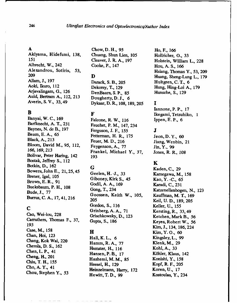
246 Ultrafast Electronics and Optoelectronics/Author Index
A Chow, D. H., 95 Ho, F., 166Akiyama, Hidefumi, 138, Chuang, Shun Lien, 105 Hollricher, 0., 33151 Cleaver, J. R. A., 197 Holstein, William L, 228Albrecht, W., 242 Cooke, P., 147 Hou, A. S., 166Alexandrou, Sotiris, 53, Hsiang, Thomas Y., 53, 209209 D Huang, Sheng-Lung L, 179Allam, J., 197 Darack, S. B., 205 Hultgren, C. T., 6Aoki, Ikuro, 112 Dekorsy, T., 129 Hung, Hing-Loi A., 179Arjavalingam, G., 126 DenBaars, S. P., 85 Hunsche, S., 129Auld, Bertram A., 112, 213 Dougherty, D. 1., 6Averin, S. V., 33, 49 Dykaar, D. R., 108, 189, 205 I
Iannone, P. P., 17B F Ikegami, Tetsuhiko, 1Banyai, W. C., 169 Falcone, R. W., 116 Ippen, E. P., 6Barfknecht, A. T., 231 Fauchet, P. M., 147, 234Baynes, N. de B., 197 Ferguson, J. F., 155 JBeam, E. A., 65 Fetterman, H. R., 175 Jeon, D. Y., 60Black, A., 213 Feuer, M. D., 216 Jiang, Wenbin, 21Bloom, David M., 95, 112, Feygenson, A., 77 Jin, Y., 99166, 169, 213 Frankel, Michael Y., 37, Jones, R. R., 108Bolivar, Peter Haring, 142 193Bostak, Jeffrey S., 112 KBotkin, D., 162 G Kaden, C., 29Bowers, John E., 21, 25, 45 Geelen, H. -J., 33 Kamegawa, M., 158Brener, Igal, 105 Giboney, Kirk S., 45 Kao, Y. -C., 65Brown, E. R., 91 Godil, A. A., 169 Karadi, C., 231Bucksbaum, P. H., 108 Gong, T., 234 Katzenellenbogen, N., 123Bude, J., 77 Goossen, Keith W., 105, Kauffman, M. T., 169Burrus, C. A., 17, 41, 216 205 Keil, U. D., 189, 205C Gordon, S., 116 Keller, U., 155Grinberg, A. A., 71 Kersting, R., 33,49Cao, Wei-lou, 228 Grischkowsky, D., 123 Ketchen, Mark B., 56Carruthers, Thomas F., 37, Gupta, S., 186 Keyes, Robert W., 56193 Kim, J., 134, 186, 224Case, M., 158 H Kim, Y. 0., 60Chan, Hoi, 123 Hall, K. L., 6 Kingsley, L., 99Chang, Kok Wai, 220 Hamm, R. A., 77 Klenk, M., 29Chemla, D. S., 162 Hamster, H., 116 Kohl, A., 33Chen, L. P., 41 Hansen, P. B., 17 K6hler, Klaus, 142Cheng, H., 201 Hashemi, M. M., 85 Konishi, Y., 158Chiu, T. H., 155 Heesel, H., 129 Kopf, R. F., 205Cho, A. Y., 41 Heinzelmann, Harry, 172 Koren, U., 17Chou, Stephen Y., 53 Hewitt, T. D., 99 Kostoulas, Y., 234
Ultrafast Electronics and Optoelectronics/Author Index 247
Kountz, Dennis J., 228 Mirin, Richard P., 21 SKovac, J., 29 Mishima, T., 197 Saild, T., 138Kruse, Th., 242 Mishra, U. K., 85 Sakaki, Hiroyuki, 138, 151Kubodera, Ken ichi, 1 Mourou, G. A., 134, 224 Schulman, J. N., 95Kula, W., 234 Schweizer, H., 29Kurz, H., 33, 49, 129, 242 N Scott, D. C., 175Kfitt, W., 129 Nagarajan, Radhakrishnan, Seabaugh, A. C., 65Kuwata-Gonokami, M., 13,25 Sha, W., 134138 Nees, John A., 186, 224 Shah, Jagdeep, 142Kyono, C. S., 37 Newkirk, M.A., 17 Shakouri, M. S., 213
Nguyen, Loi D., 82 Shealy, J. B., 85L Norris, T. B., 134 Shen, Zhi-Yuan, 228
Lai, Yi-Sern, 228 Nuss, Martin C., 105, 216 Shimizu, Mitsuaki, 21
Law, H. H., 216 Shunk, S. C., 216Lee, Chi H., 179, 228 0 Silvestre, Pierre, 45Lee, K. F., 60 Ogawa, K., 197 Smith, P. R., 77, 216Leisching, Patrick, 142 Ohbu, L, 197 Sobolewski, Roman, 209,
Lenz, G., 6 Orenstein, J., 231 234Leo, Karl, 33, 49, 129, 142, Oshita, F. K., 175 Son, J., 134, 224242 Ozbay, E., 95 Sorin, Wayne V., 220
Levi, A. F. J., 205 Spangenberg, B., 33Lin, S. Y., 126 p Sullivan, A., 116Liu, C. T., 41 Pan, Ci-Ling, 183Liu, J. M., 41 Pang, Philip, 228 TLiu, Mark Y., 53 Pfeifer, T., 129 Tadayon, Bijan, 193Liu, Yongqian, 238 Pfeiffer, Loren N., 105, 205 Tang, Kai-Yuan, 183Liu, Yuan-Qun, 228 Planken, Paul C. M., 105 Tanoue, T., 197Lobad, A. I., 147 Plant, D. V., 175 Tauber, Dan, 25Lu, T. -M., 119 Platt, Christine E., 238 Tennant, D. M., 60Luo, Marie S. C., 105 Plettner, J., 33, 49 Thiagarajan, Prabhu, 45
Luryi, S., 71 Tousley, B. C., 147Luscombe, J. H., 65 R
M Randall, J. N., 65 UM Raybon, G., 17 Ucer, K. B., 234Ma, X. F., 99 Reynolds, Thomas E., 21Mao, S. N., 228 Richards, P. L., 231 VMartin, M., 175 Ritter, Dan, 77 Van Der Weide, Daniel W.,
Matsusue, Toshio, 138, 151 Robertson, W. M., 126 112McClelland, Gary M., 172 Robinson, Gary Y., 45 Venkatesan, T., 228
Mears, C. A., 231 Rodney, P. J., 147 Verghese, S., 231Mehta, S. M., 147 Rodwell, Mark 3. W., 45, Von Kamienski, E. Stein,Mikkelsen, H., 129 158 33Miller, B. ., 17 Roskos, H. G., 33
248 Ultrafast Electronics and Optoelectronics/Author Index
W Wey, Yih-Guei, 45 YWakana, S., 224 Whitaker, John F., 134, Yakymyshyn, C. P., 119Wang, Chia-Chi, 209 201,224,238 Yan, R. H., 60Wang, Gary, 25 White, J., 197 You, D., 108Watanabe, Fumiya, 172 White, W., 116 Young, M.G., 17Weiner, M., 99 Williamson, S., 186, 224 Yu, R., 158Weingarten, K. J., 155 Wu, Hsiao-Hua, 183Weinmann, R., 29 ZWeiss, S., 162 X Zhang, X. -C., 99,119West, K. W., 205 Xi, X. X., 228 Zheng, L. X., 234Westerwick, E. H., 60 Xiong, W., 234 Zielinski, E., 29


