Embed Size (px)
Citation preview
Vertical H
eterostru
cture III-V
Nan
ow
ire MO
SFETs
Department of Electrical and Information Technology, Faculty of Engineering, LTH, Lund University, 2016.
Vertical Heterostructure III-VNanowire MOSFETs
Adam Jönsson
Series of Master’s thesesDepartment of Electrical and Information Technology
LU/LTH-EIT 2016-537http://www.eit.lth.se
Ad
am
Jön
sson
Master’s Thesis
Vertical Heterostructure III-V NanowireMOSFETs
Adam Jö[email protected]
Department of Electrical and Information TechnologyLund University
Supervisors: Lars-Erik Wernersson & Olli-Pekka Kilpi
August 31, 2016

Printed in SwedenE-huset, Lund, 2016
Abstract
"If cars had developed as fast as processors they would go at 470,000 mph,get 100,000 miles to the gallon, and cost 3 cents" claims Paul Ottelini, Intel
CEO 2005-2013. This serves as a reminder of how fast the field of nanoelectronicsis developing due to constant demand for faster and more energy efficient inte-grated circuits. The still ongoing electronics revolution was accelerated by theinnovation of one simple and elegant device, namely the Si-based metal-oxide-semiconductor-field-effect-transisor MOSFET in 1959. The pillar of economicgrowth has since been based on downscaling the MOSFET and increasing thedensity of transistor per chip area. Downscaling of the transistor has favourablyled to more efficient and faster devices. MOSFETs today are approaching sizeswhich only include few monolayers of atoms, basically dimensions of a fewnanometer. Conventional electronics has thus been pushed into the quantumrealm forcing future improvements to be based on innovation rather than sim-ply downscaling. To win the battle against Heisenberg’s uncertainty leading toleakage currents and various other effect due to reduced size, new 3d geometrieshas been introduced. Amongst these new geometries is the bottom up approachutilizing vertical nanowires. The vertical geometry also enables easier integra-tion of alternative high mobility semiconductor materials on a Si substrate. Apotential canditate for integration on Si is the III-V compound semiconductorsdue improvements in charge carrier transport capabilities.
To further motivate a switch in transistor geometry the full infrastructure ofdevices need to be present, not only satisfying the logical domain. Therefore, inparallel to the digital branch, a wish for developing better analog RF-transistors ispresent. The requirements for an RF-transistor are quite different where stabilityand high frequency signal gain is of importance. In an RF circuit power dissi-pation can be sacrificed for increased performance, lending more room for newinnovations.
In this thesis the use of the vertical nanowire geometry for MOSFET is fur-ther investigated by implementing a III-V, InAs/InGaAs, graded heterostructure,inside the channel, optimized for increased stability and low resistance ohmic-contacts. A Si-substrate with grown III-V nanowires, on top of a InAs bufferlayer, is provided and afterwards processed into a complete set of devices. Theorientation of the grading is chosen with an abrupt junction from the InAs bufferlayer to InGaAs slowly graded back to InAs at the top, by implementing 550
i
nm long nanowires. The measured DC-characteristics indicates a presence of theheterostructure due to good saturation, low output conductance gd ≈ 2 µS/µm atVds = 0.5V and Vgs = 0.5V. Amplification and current does not reach intendedvalues because of large access resistance, Rc ≈ 1500 Ωµm, with transconductancegm,max = 280 µS/µm. Good gate control is indicated with devices showcasing lowsub-threshold swing SS down to 80 mV/dec.
Motivation of introducing a heterostructure is clear due to higher breakdownand increased linearity but the choice of the grading orientation is not. Contactresistance is mostly originating from the source side, which means that there islarge room for improvement by tweaking the process. The nanowires also had atendency to collapse which decreased the performance. In other words the theoryof implementing a heterostructure with abrupt junction for larger breakdownvoltage and increased linearity is promising and cannot yet be disregarded.
ii
PopulärvetenskapligSammanfattning
"Om bilar hade utvecklats så snabbt som processorer skulle de färdas i enhastighet på 760,000 km/h, gå 42 000 km per liter och kosta 25 öre" hävdar
Paul Ottelini, Intel VD mellan 2005-2013. Detta påminner oss om vilken rasandefart utvecklingen har inom nanoelektronik branschen där elektroniska kretsarständigt blivit billigare samt mindre under det senaste halvseklet. Miniatyriserin-gen har fördelaktigt gått hand i hand med ökad prestanda. Den huvudsakligabeståndsdelen som används i dessa kretsar, som exempelvis en processor, är entransistor. Uppgiften för en transistor är att styra strömmar på så sätt att de kanstängas av eller på.
Transistorn består av tre huvudsakliga elektroder, där elektrisk spänning kanappliceras. Mellan två av elektroderna kan en ström färdas såsom igenom ettvanligt motstånd. Med den tredje, som brukar kallas gate, kan resistansen ma-nipuleras vilket ändrar strömmen som färdas mellan de två övriga elektroderna.I en dator krävs det att transistorn ska fungera som ett relä, helt enkelt en effektivav/på knapp. Här är prestandan väldigt beroende av hur många transistorer,logiska kretsar, som får plats på ett chip för att i slutändan kunna utföra mångaberäkningar samtidigt.
För analoga applikationer däremot, i till exempel radiosändare och mottagare,ställs andra krav. Här kan det räcka med endast ett fåtal transistorer som effektivtkan tolka och förstärka en signal som varierar över tiden. När frekvensen påsignalen som ska sändas, eller mottagas, ökar kan även mer information trans-porteras. I framtiden krävs därmed pålitliga transistorer som hinner tolka snabbaströmändringar på grund av signal-frekvenser på flera 100 GHz.
I den digitala världen har den pågående miniatyriseringen av de logiskakretsarna lett till att många dimensioner endast är tiotals atomer. Därmed upp-kommer flera utmaningar vid vidare miniatyrisering av kretsarna som leder tillatt man fullkomligt förlorar kontrollen över gaten. För fortsatt utveckling tittarman då på alternativa material samt andra utformningar av transistorerna. Dettål att nämnas att det som sker i den digitala världen självklart påverkar denanaloga sfären.
I detta arbete har möjligheten att skapa transistorer av stående cylindriskapelare, även kallade nanotrådar, undersökts. På dessa nanotrådar kan gaten lin-
iii

das runt själva tråden för att få bästa möjliga kontroll av strömmen. Dessutom ärolika material blandade inuti tråden för att uppnå gynnsamma villkor. Dessavillkor är att elektroner enkelt ska kunna färdas genom materialet samtidigtsom transistorn ska vara pålitlig vid ett stort omfång av applicerad spänningpå elektroderna. Därför har en blandning av indiumarsenid, som bidrar medhög rörlighet för elektroner, och indiumgalliumarsenid använts. Det sistnämndamaterialet bidrar med extra pålitlighet. Den färdiga transistorn uppvisade godkontroll av strömmen med aningen begränsad prestanda. Notera att dessa tran-sistorer är, i grund och botten, skapade ovanpå ett kiselprov, vilket gör dennateknologi överförbar till industriell skala.
iv
Acknowledgements
"Now this is not the end. It is not even the beginning.But it is perhaps the end of the beginning."
Sir Winston Leonard Spencer-Churchill
My time as a student at Lunds University is coming to an end, or perhaps,a new beginning. When my interests of continuing on the academic path whereflailing, a few people made me realise my potential. Among these people thereare a two professors in particular, namely Dan Hessman and Lars-Erik Werners-son. The pursuit itself is priceless and the end result is necessarily not the mostimportant. This is the way of the researcher. So from the bottom of my heart Iwould like to thank you for all your support.
I would also like to extend my gratitude to my practical coach Olli-Pekka, whotirelessly taught me a very long and complicated process, and Johannes Svensson,who had to developed an all new nanowire growth recipe. I am greatly humbledby the skill level possessed by these individuals.
My family has always been a source for inspiration and pushing me to pursuemy dreams, therefore I thank Lars, Charita and Max.
v

vi

Abbreviations & symbols
Abbreviations
ADC analogue-to-digital converterALD atomic layer depositionAl2O3 aluminium oxideAr argonAs arsenicAsH3 arsineAu gold
BOE buffered oxide etchBTBT band-to-band tunneling
C carbon
DR double row arrayEBL electron beam litography
GAA gate all-aroundGaAs gallium arsenideGaN gallium nitrideGaSb gallium antimonideGe germanium
HBT heterojunction bipolar transistorHEMT high electron mobility transistorHF hydro fluorideHfO2 hafnium dioxideHSQ hydrogen silsesquioxane
vii

ICP-RIE inductively coupled plasma reactive-ion etchingIn indiumInAs indium arsenideInGaAs indium gallium arsenideInP indium phosphideInSb indium antimonideIPA 2-propanol
MESFET metal-semiconductor field effect transistorMOSFET mteal-oxide-semiconductor field effect transistorMOVPE metalorganic vapour phase epitaxy
N2 nitrogenNi nickelNW nanowireNWFET nanowire field effect transistor
O oxygen
PMMA poly(methyl methacrylate)
RF Radio frequencyRIE reactive-ion etcher
SEM scanning electron microscopySi siliconSiO2 silicon dioxideSiO silicon monoxideSn tin
TESn tetraethyltinTFET tunnel field effect transistorTiN titanium nitrideTMAH tetramethylammonium hydroxideTMGa tetramethylgalliumTMIn tetramethylindium
UV ultravioletUVL ultraviolet litography
VLS vapor-liquid-solid
W tungsten
viii

Physical constants
ε0 vacuum permittivity 8.854 ∗ 10−12 F/mkB boltzmanns constant 8.617 ∗ 10−5 eV/Ke eulers number 2.718q elementary charge 1.602 ∗ 10−19 C
Symbols
a lattice constant mA area m2
Av open circuit amplification -Cox intrinsic oxide capacitance F/m2
Cgd gate-drain capacitance F/m2
Cgs gate-source capacitance F/m2
d distance mDit density of interface traps m−3
EC conduction band energy eVEF fermi-level eVEg band gap eVEV valence band energy eVft cut-off frequency Hzgd output conductance Sgm transconductance SIds drain-source current AIon on-state current AIon off-state current ANd donors m−3
Na acceptors m−3
Vds drain-source voltage VVgs gate-source voltage VVt threshold voltage VRch channel resistance ΩmRd drain resistance ΩmRc access resistance ΩmRon on-resistance ΩmRs source resistance ΩmSS sub-threshold slope mV/dec
ix

εr relative permittivity -κ dielectric constant F/mµe electron mobility cm2V−1s−1
µp hole mobility cm2V−1s−1
φB Schottky barrier potential VφM metal work function Vφs semiconductor work function Vχs semiconductor electron affinity V
x

Table of Contents
1 Introduction 11.1 Semiconductor Physics . . . . . . . . . . . . . . . . . . . . . . . . . 21.2 Background & Future of MOSFET . . . . . . . . . . . . . . . . . . . 5
2 MOSFET Performance Metrics 132.1 On-resistance . . . . . . . . . . . . . . . . . . . . . . . . . . . . . . . 142.2 Output Conductance . . . . . . . . . . . . . . . . . . . . . . . . . . . 142.3 Transconductance . . . . . . . . . . . . . . . . . . . . . . . . . . . . 152.4 Threshold Voltage . . . . . . . . . . . . . . . . . . . . . . . . . . . . 152.5 Voltage Gain . . . . . . . . . . . . . . . . . . . . . . . . . . . . . . . 162.6 Subthreshold Swing . . . . . . . . . . . . . . . . . . . . . . . . . . . 162.7 Cut-off Frequency . . . . . . . . . . . . . . . . . . . . . . . . . . . . 16
3 MOSFET Evolution 17
4 MOSFET Fabrication 214.1 Nanowire Growth . . . . . . . . . . . . . . . . . . . . . . . . . . . . . 224.2 Top Metal Deposition . . . . . . . . . . . . . . . . . . . . . . . . . . . 234.3 Drain Pad and Bottom Spacer . . . . . . . . . . . . . . . . . . . . . 244.4 Gate Deposition . . . . . . . . . . . . . . . . . . . . . . . . . . . . . 254.5 Via Holes and Top Contact . . . . . . . . . . . . . . . . . . . . . . . 27
5 Result & Analysis 295.1 Processing . . . . . . . . . . . . . . . . . . . . . . . . . . . . . . . . 295.2 Measurements . . . . . . . . . . . . . . . . . . . . . . . . . . . . . . 325.3 Benchmarking . . . . . . . . . . . . . . . . . . . . . . . . . . . . . . 375.4 Breakdown . . . . . . . . . . . . . . . . . . . . . . . . . . . . . . . . 38
6 Conclusion & Outlook 41
References 43
A Batch #1 metrics 47
xi

xii
List of Figures
1.1 A simplified sodium crystal containing only three atoms to modelthe total potential seen by the charge carriers. The valence elec-trons in the structure are shared, and can move between atoms.(a) The potential for the free charge carriers can be modelled by asimple square potential where local potential shift originating fromthe atomic nucleus is neglected. This modelling is sufficient to in-troduce the concept of effective mass. (b) Another layer is addedto the model where a periodic pertubation, depending on latticeconstant a, is added. Crucial for the derivation of energy band gapseen by free charge carriers. . . . . . . . . . . . . . . . . . . . . . . 3
1.2 A typical shift in fermi-level EF during different doping. The intrin-sic Fermi level EF,i resides in the middle of the band gap meaningthat few free carriers are available and the material is highly re-sistive. The amount of free carriers n or p at room temperature isinversely dependant on the band gap 1
Eg. When adding donors Nd
to the semiconductor the fermi level is shifted upwards to EF,n andin this case reaches above degenerate limit meaning that chemi-cal potential is inside the conduction band. The same shift occursdownwards in energy when adding acceptors Na and the potentialends up at EF,p. . . . . . . . . . . . . . . . . . . . . . . . . . . . . . . 3
1.3 Dense version of the periodic table with atoms involved in highspeed electronic devices. III-V compounds with typical dopants Snor Si can give both p and n-doping. Source: Wikimedia Commons 4
1.4 The formed Schottky barrier, according to Schottky-Mott rule, in ametal-semiconductor junction. The height of the barrier is deter-mined by the difference between metal work function φM and elec-tron affinity of the semiconductor χs, see equation 1.1. Work func-tion of the semiconductor φs is also given. Notice that W depictsthe width of the depletion region in the semiconductor in which theband bending takes place. . . . . . . . . . . . . . . . . . . . . . . . 5
xiii
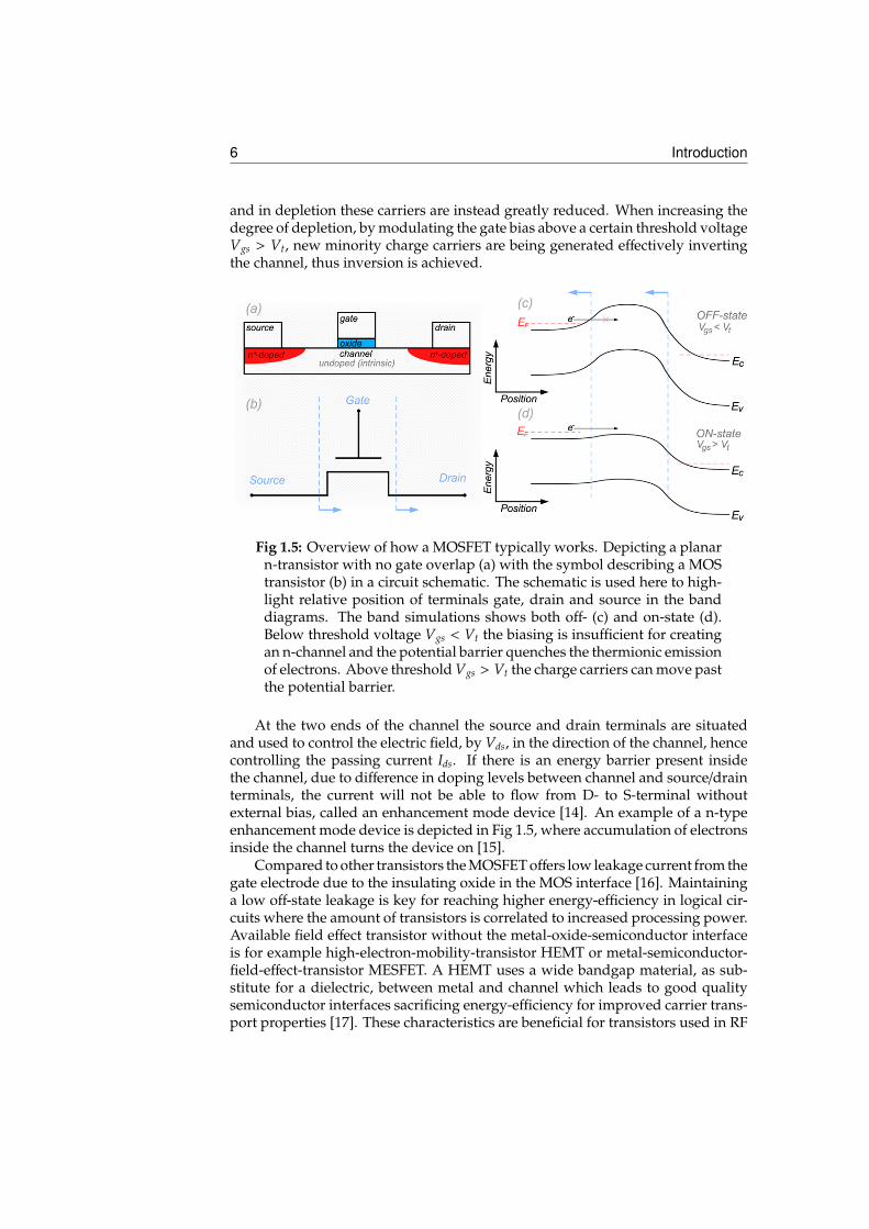
1.5 Overview of how a MOSFET typically works. Depicting a planarn-transistor with no gate overlap (a) with the symbol describinga MOS transistor (b) in a circuit schematic. The schematic isused here to highlight relative position of terminals gate, drainand source in the band diagrams. The band simulations showsboth off- (c) and on-state (d). Below threshold voltage Vgs < Vtthe biasing is insufficient for creating an n-channel and the poten-tial barrier quenches the thermionic emission of electrons. Abovethreshold Vgs > Vt the charge carriers can move past the potentialbarrier. . . . . . . . . . . . . . . . . . . . . . . . . . . . . . . . . . . 6
1.6 Innovation flow in commercial logic transistors presented by In-tel [18]. Change in high κ was implemented in order to increasegate-thickness supressing leakage currents. 3d structures (lateralnanowires) for increased electrostatics has also already been in-troduced. . . . . . . . . . . . . . . . . . . . . . . . . . . . . . . . . . 7
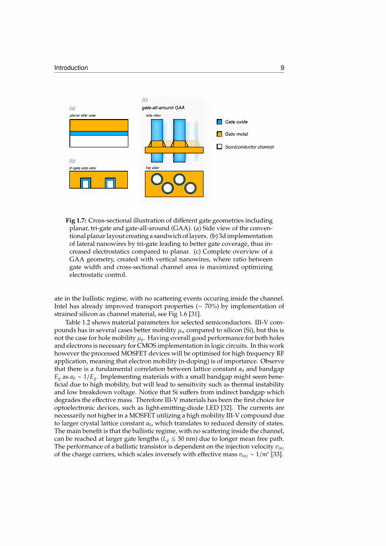
1.7 Cross-sectional illustration of different gate geometries includingplanar, tri-gate and gate-all-around (GAA). (a) Side view of theconventional planar layout creating a sandwich of layers. (b) 3dimplementation of lateral nanowires by tri-gate leading to bettergate coverage, thus increased electrostatics compared to planar.(c) Complete overview of a GAA geometry, created with verticalnanowires, where ratio between gate width and cross-sectionalchannel area is maximized optimizing electrostatic control. . . . . . 9
1.8 Effects during high bias conditions. In impact ionization electronsin the conduction band gain enough energy, due to an externalelectric field, to create extra electron-hole pairs during a scatteringevent. With BTBT (band-to-band-tunneling) the potential barrier issufficiently thin to allow quantum tunneling, also generating extraelectron hole-pairs. . . . . . . . . . . . . . . . . . . . . . . . . . . . . 11
2.1 A schematic of a MOSFET indicating the biasing points for anintrinsic device with added series resistance. Source is normallyconnected to ground as a reference which means that biasing iscontrolled through the gate Vgs and drain Vds electrodes. Biasingresults in pulling a current from drain to source Ids. . . . . . . . . . 13
2.2 Output conductance of an actual MOSFET, illustrating extractionof gd and Ron. Notice that on-resistance Ron is extracted below thesaturation region and given as the inverse of the derivative. . . . . 14
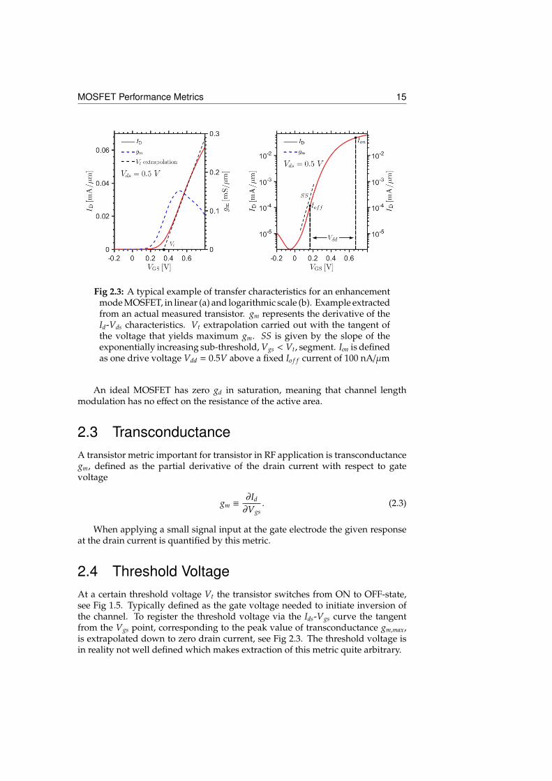
2.3 A typical example of transfer characteristics for an enhancementmode MOSFET, in linear (a) and logarithmic scale (b). Exampleextracted from an actual measured transistor. gm represents thederivative of the Id-Vds characteristics. Vt extrapolation carried outwith the tangent of the voltage that yields maximum gm. SS isgiven by the slope of the exponentially increasing sub-threshold,Vgs < Vt, segment. Ion is defined as one drive voltage Vdd = 0.5Vabove a fixed Io f f current of 100 nA/µm . . . . . . . . . . . . . . . . 15
xiv
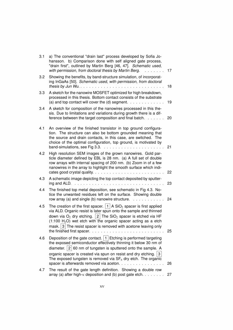
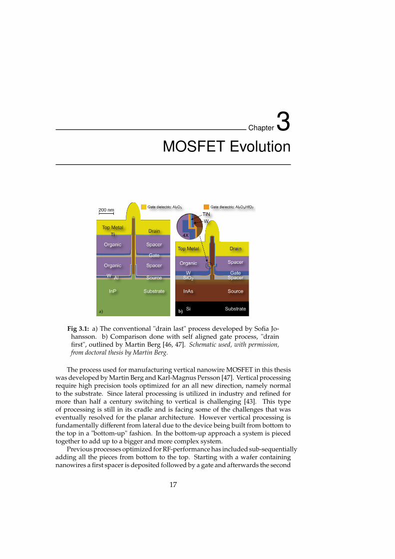
3.1 a) The conventional "drain last" process developed by Sofia Jo-hansson. b) Comparison done with self aligned gate process,"drain first", outlined by Martin Berg [46, 47]. Schematic used,with permission, from doctoral thesis by Martin Berg. . . . . . . . 17
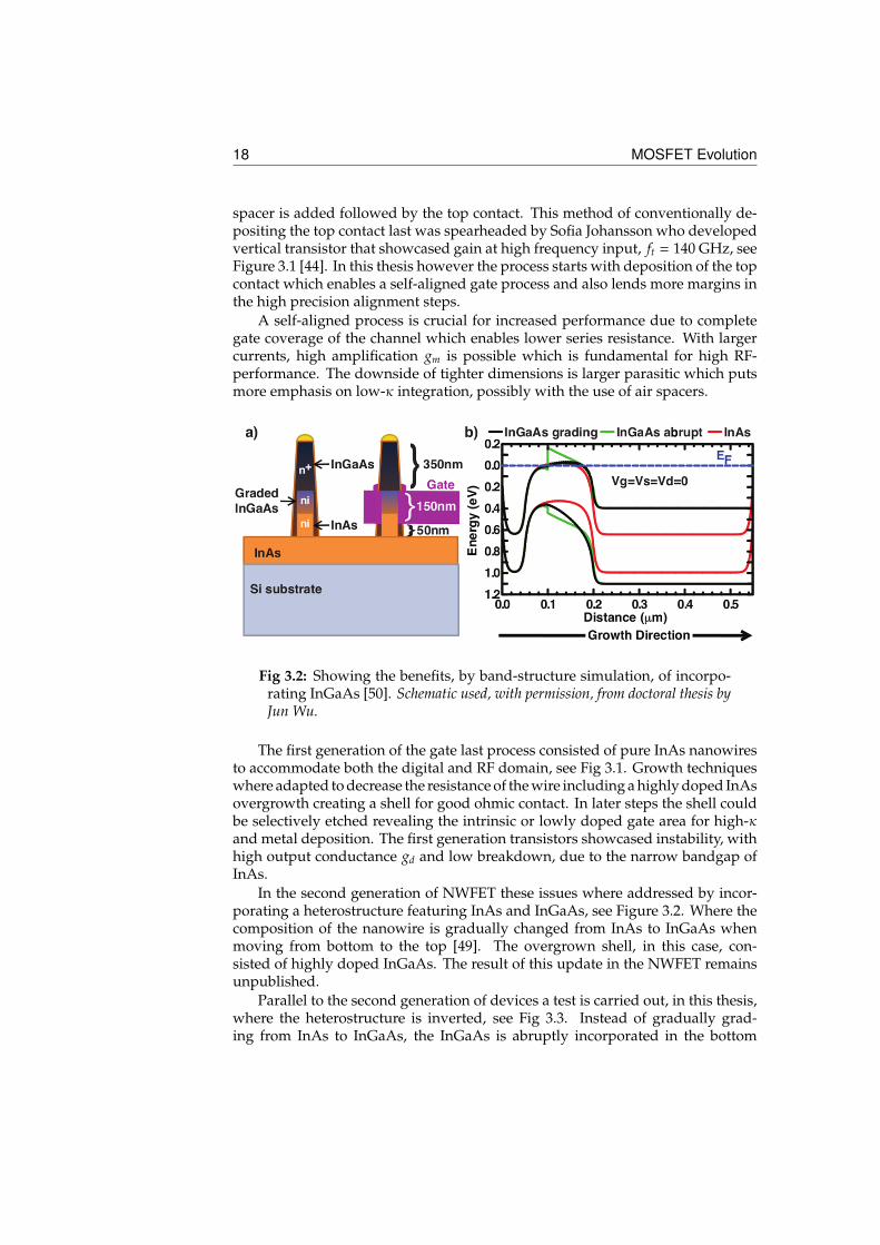
3.2 Showing the benefits, by band-structure simulation, of incorporat-ing InGaAs [50]. Schematic used, with permission, from doctoralthesis by Jun Wu. . . . . . . . . . . . . . . . . . . . . . . . . . . . . . 18
3.3 A sketch for the nanowire MOSFET optimized for high breakdown,processed in this thesis. Bottom contact consists of the substrate(a) and top contact will cover the (d) segment. . . . . . . . . . . . . 19
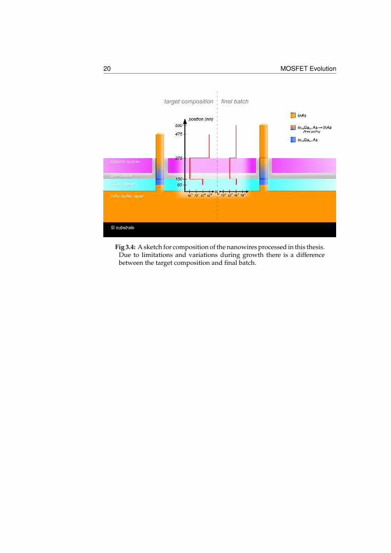
3.4 A sketch for composition of the nanowires processed in this the-sis. Due to limitations and variations during growth there is a dif-ference between the target composition and final batch. . . . . . . 20
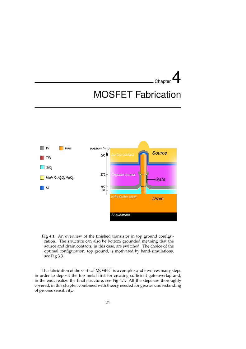
4.1 An overview of the finished transistor in top ground configura-tion. The structure can also be bottom grounded meaning thatthe source and drain contacts, in this case, are switched. Thechoice of the optimal configuration, top ground, is motivated byband-simulations, see Fig 3.3. . . . . . . . . . . . . . . . . . . . . . 21
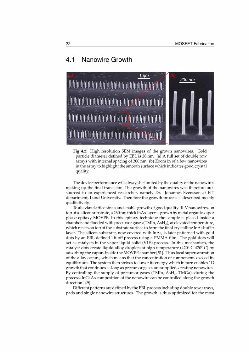
4.2 High resolution SEM images of the grown nanowires. Gold par-ticle diameter defined by EBL is 28 nm. (a) A full set of doublerow arrays with internal spacing of 200 nm. (b) Zoom in of a fewnanowires in the array to highlight the smooth surface which indi-cates good crystal quality. . . . . . . . . . . . . . . . . . . . . . . . . 22
4.3 A schematic image depicting the top contact deposited by sputter-ing and ALD. . . . . . . . . . . . . . . . . . . . . . . . . . . . . . . . 23
4.4 The finished top metal deposition, see schematic in Fig 4.3. No-tice the unwanted residues left on the surface. Showing doublerow array (a) and single (b) nanowire structure. . . . . . . . . . . . 24
4.5 The creation of the first spacer. 1 A SiO2 spacer is first appliedvia ALD. Organic resist is later spun onto the sample and thinneddown via O2 dry etching. 2 The SiO2 spacer is etched via HF(1:100 H2O) wet etch with the organic spacer acting as a etchmask. 3 The resist spacer is removed with acetone leaving onlythe finished first spacer. . . . . . . . . . . . . . . . . . . . . . . . . . 25
4.6 Deposition of the gate contact. 1 Etching is performed targetingthe exposed semiconductor effectively thinning it below 30 nm ofdiameter. 2 60 nm of tungsten is sputtered onto the sample. Aorganic spacer is created via spun on resist and dry etching. 3The exposed tungsten is removed via SF6 dry etch. The organicspacer is afterwards removed via aceton. . . . . . . . . . . . . . . . 26
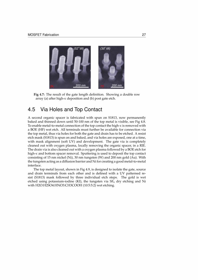
4.7 The result of the gate length definition. Showing a double rowarray (a) after high-κ deposition and (b) post gate etch. . . . . . . . 27
xv
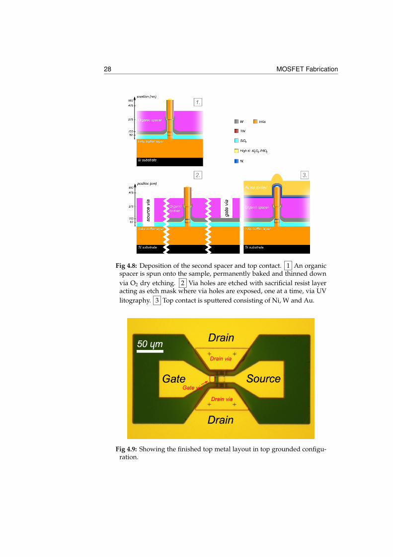
4.8 Deposition of the second spacer and top contact. 1 An organicspacer is spun onto the sample, permanently baked and thinneddown via O2 dry etching. 2 Via holes are etched with sacrificialresist layer acting as etch mask where via holes are exposed, oneat a time, via UV litography. 3 Top contact is sputtered consistingof Ni, W and Au. . . . . . . . . . . . . . . . . . . . . . . . . . . . . . 28
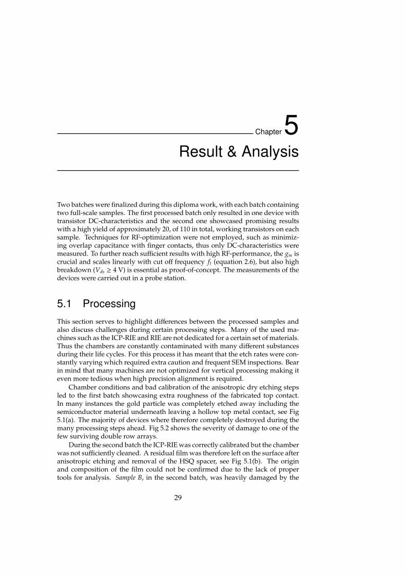
4.9 Showing the finished top metal layout in top grounded configuration. 28
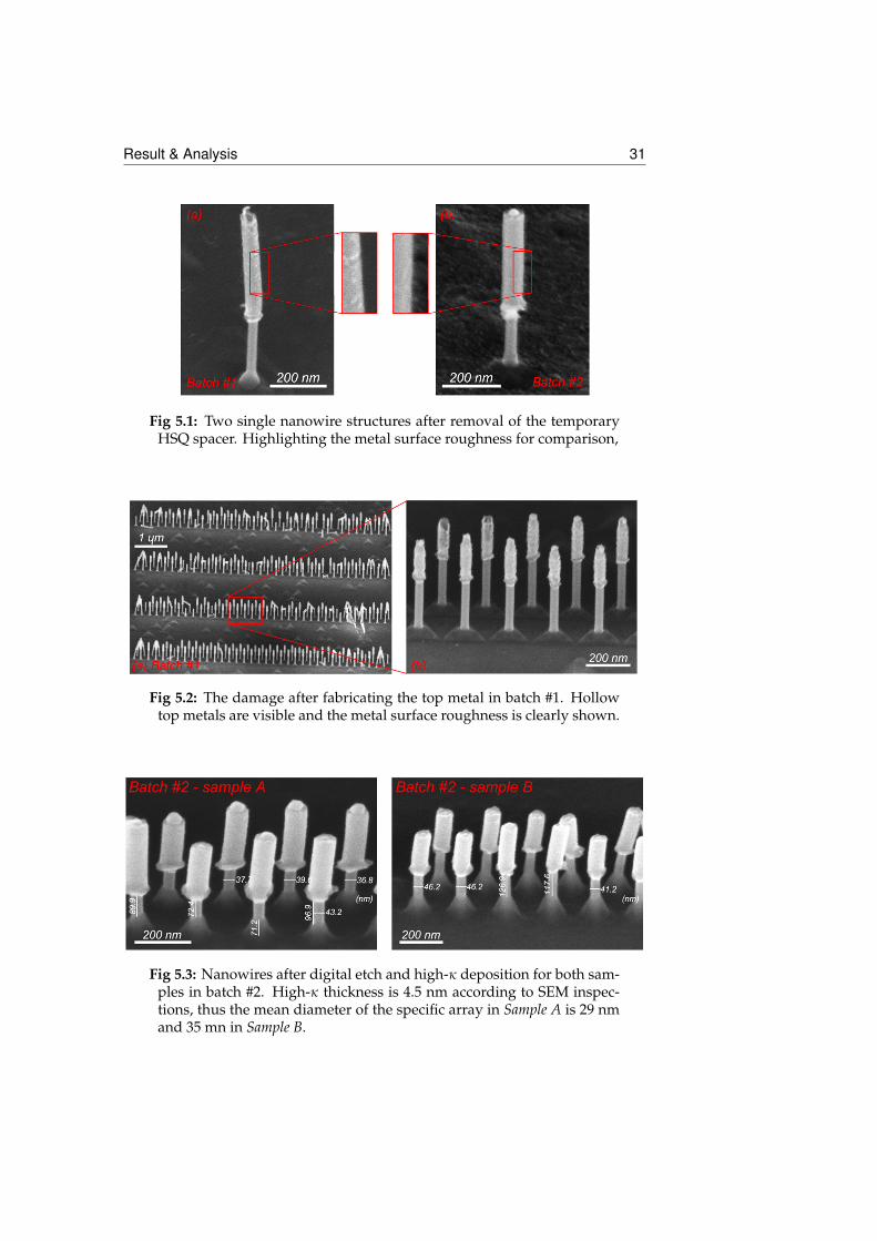
5.1 Two single nanowire structures after removal of the temporaryHSQ spacer. Highlighting the metal surface roughness for com-parison, . . . . . . . . . . . . . . . . . . . . . . . . . . . . . . . . . . 31
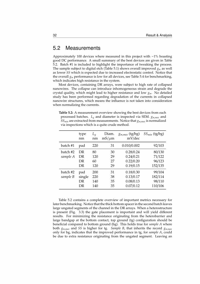
5.2 The damage after fabricating the top metal in batch #1. Hollow topmetals are visible and the metal surface roughness is clearly shown. 31
5.3 Nanowires after digital etch and high-κ deposition for both sam-ples in batch #2. High-κ thickness is 4.5 nm according to SEMinspections, thus the mean diameter of the specific array in Sam-ple A is 29 nm and 35 mn in Sample B. . . . . . . . . . . . . . . . 31
5.4 Overview of all arrays in batch 2. No sidewall etch was performedon sample B, meaning that the effective diameter of the nanowiresare smaller in sample A, see Table 5.1. (a)-(b) shows the correla-tion between extracted values Ron and gm,max, clearly showing theexpected exponential trend when decreasing the total resistance.(c)-(d) Outlines SS dependence of gm,max, showing no clear trend. 33
5.5 Exhibiting the SS-Vt and Ron-Lg dependence. Attempts for extrap-olating the access resistance, Rc = Rs + Rd, are performed withtaking all values into account (#1) and a selected few (#2) thatare highlighted. A smaller ratio of collapsed nanowires seem tobe present in the highlighted devices. Note that the Lg values arebased on estimates from SEM pictures that, in this case, might beinsufficient due to large thickness variation of the bottom spacer. . 34
5.6 Transfer characteristics, plotted in logarithmic scale, for the herodevice found batch #2. Metrics compiled in Fig 5.2.1. . . . . . . . . 35
5.7 Output characteristics for the hero device found batch #2. Metricscompiled in Fig 5.2.1. . . . . . . . . . . . . . . . . . . . . . . . . . . 36
5.8 Output characteristics for a representative, double row, device atbias conditions close to its breakdown at 4 V. The device is foundbatch #2-sample A. The transistor can operate up to 3.5 V, butshowcases bad saturation with high gd. Different segments canbe identified with (a) being well saturated and (b) showing impactionization that accelerates further in (c). . . . . . . . . . . . . . . . . 38
5.9 Comparing output characteristics for top and bottom ground con-figuration in a representative, double row, device. The device isfound batch #2-sample A. The transistor breaks at 2.2 V in bot-tom ground. Different segments can be identified with (a) beingwell saturated and (b) showing impact ionization that acceleratesfurther in (c). . . . . . . . . . . . . . . . . . . . . . . . . . . . . . . . 39
xvi
List of Tables
1.1 Comparing dielectrics materials that are generally used for MOS-FET. Both large offset ∆Ec,InAs and bandgap is crucial for reductionof leakage. [24] . . . . . . . . . . . . . . . . . . . . . . . . . . . . . 8
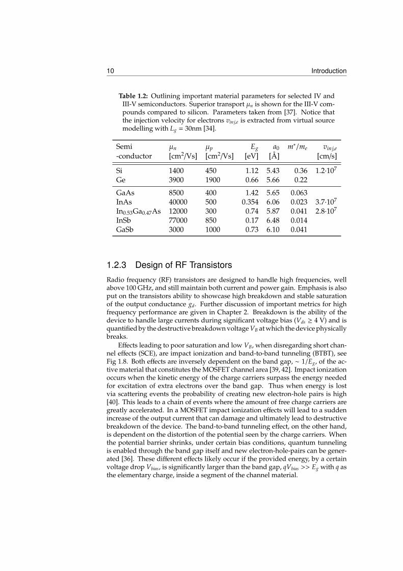
1.2 Outlining important material parameters for selected IV and III-Vsemiconductors. Superior transport µn is shown for the III-V com-pounds compared to silicon. Parameters taken from [37]. Noticethat the injection velocity for electrons vinj,e is extracted from virtualsource modelling with Lg = 30nm [34]. . . . . . . . . . . . . . . . . . 10
5.1 A quick comparison between processed samples. 1Top contactquality and gate alignment greatly improved between batches, withthe first batch having ∼ 20 nm of ungated channel area. 2All pro-cessing was optimized for the double row (DR) arrays in the sec-ond batch. The gate length is varying between devices due toboth the bottom spacer and position of the top contact. . . . . . . . 30
5.2 A measurement overview showing the best devices from each pro-cessed batches. Lg and diameter is inspected via SEM. gm,max andSSmin are extracted from measurements. Notice that gm,max is nor-malized via inspections which is a quite crude method. . . . . . . 32
5.3 Outlining all metrics for the best device in batch #1. Values areextracted from SEM inspections. All data is normalized to the totalcircumference of the nanowires. 1Bias conditions are chosen inactive region of the transistor at Vg = 0.5 and Vds = 0.5V. . . . . . . 36
5.4 A comparison with mainly other work from the research group (Na-noelectronics Group), created in the same lab using mostly thesame equipment. V highlight the vertical orientation of the device,other devices utilize a lateral geometry. Notice that all V-NW de-vices are integrated on silicon while the both the HEMT and recorddevice are based on an InP(III-V) substrate. . . . . . . . . . . . . . 37
xvii

A.1 Outlining all metrics for the best device in batch #1. Values areextracted from SEM inspections. All data is normalized to the to-tal circumference of the nanowires. 1A mean value has been ex-tracted from SEM inspections of other pads 2Bias conditions arechosen in active region of the transistor at Vg = 0.5 and Vds = 0.6V. 47
xviii
Chapter1Introduction
In the year 1925 Julius Edgar Lilienfeld filed a patent for the field effect transistorFET, describing the basics of what later would be known as the metal-oxide-
semiconductor field effect transistor MOSFET [1]. Due to high purity semiconduc-tors not being available the concept was experimentally confirmed decades laterby Bell Labs in 1948. Further development was, at the time, not pursued due toproblems connected to the surface of the semiconductor. Instead the germaniumbased point-contact transistor, invented in 1947, stole the show and became com-mercially available for use in the early pocket radios, replacing the bulky vacuumtubes [2]. Connected to improvement in semiconductor quality and advent ofintegrated circuits (ICs) based on silicon in the 1960s the dreams of the MOSFETonce again resurfaced. At this point the interface problems had been resolvedby means of taming the strong native oxide found in silicon. The emergence ofthe computer industry further pushed the revolution with constant demands forfaster and more energy efficient circuits.
Gordon E. Moore released his predictions (Moore’s law) in 1965 stating thatthe number of transistors per chip area will roughly double every 24 monthsvia geometrical downscaling [3]. The predictions was based on the fact thatincreased packing density leads to exponential increase in performance as wellas lower power dissipation of the circuits. Moore’s law was followed strictly upuntil 2002 when the downscaling became constricted by power dissipation of 100W/cm2 [4]. To avoid overheating increase of performance was now pursued withmulti-core systems and parallelization of computer tasks rather than speed.
Today the industry is in a place where things are shaken up with uncertainty.Improvements in transistor technology is now heavily dependent on innovationsrather than downscaling. The technology demands has also changed with the up-coming era of IoT (Internet of things) setting up new standards for RF-transistorsused in wireless communications [5]. A potential candidate for meeting the de-mands is to integrate III-V high speed material, on silicon substrates, utilizing ananowire geometry with gate all-around (GAA) configuration. This alternativeis further examined in this thesis. The needed background for absorbing andunderstanding the benefits of the work in this thesis is given in this chapter.
1
2 Introduction
1.1 Semiconductor PhysicsTo grasp the concept of transistor technology it is important to have a fundamen-tal understanding of its building blocks, namely the semiconductor. Normally asemiconductor consists of a solid chemical element or compound, for example III-V semiconductors, and is used for integrated circuits due to its ability to conductelectricity during some circumstances but not others. To explain this behaviourconcepts of chemical potential and band gap are introduced. An intrinsic semi-conductor has its chemical potential, described by Fermi-Dirac statistics, placedinside the band gap typically ranging from 0.5 up to 8 eV. Few charge carriersare typically available in a semiconductor leading to poor conductance. To cir-cumvent this issue doping is introduced increasing the amount of charge carriersinside the conduction band. The concepts are further explained in this chapter.
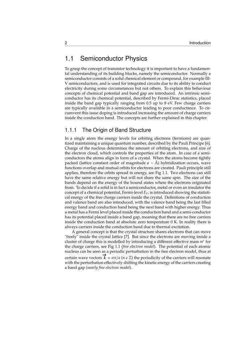
1.1.1 The Origin of Band StructureIn a single atom the energy levels for orbiting electrons (fermions) are quan-tized maintaining a unique quantum number, described by the Pauli Principe [6].Charge of the nucleus determines the amount of orbiting electrons, and size ofthe electron cloud, which controls the properties of the atom. In case of a semi-conductors the atoms align in form of a crystal. When the atoms become tightlypacked (lattice constant order of magnitude a ∼ Å) hybridization occurs, wavefunctions overlap and mutual orbits for electrons are created. Pauli principle stillapplies, therefore the orbits spread in energy, see Fig 1.1. Two electrons can stillhave the same relative energy but will not share the same spin. The size of thebands depend on the energy of the bound states where the electrons originatedfrom. To decide if a solid is in fact a semiconductor, metal or even an insulator theconcept of a chemical potential, Fermi-level EF, is introduced showing the statisti-cal energy of the free charge carriers inside the crystal. Definitions of conductionand valence band are also introduced, with the valence band being the last filledenergy band and conduction band being the next band with higher energy. Thusa metal has a Fermi level placed inside the conduction band and a semi-conductorhas its potential placed inside a band gap, meaning that there are no free carriersinside the conduction band at absolute zero temperature 0 K. In reality there isalways carriers inside the conduction band due to thermal excitation.
A general concept is that the crystal structure shares electrons that can move"freely" inside the crystal lattice [7]. But since the electrons are moving inside acluster of charge this is modelled by introducing a different effective mass m∗ forthe charge carriers, see Fig 1.1 (free electron model). The potential of each atomicnucleus can be seen as a periodic perturbation in the free electron model, thus at
certain wave vectors−→k = nπ/a (n ε Z) the periodicity of the carriers will resonate
with the perturbation effectively shifting the kinetic energy of the carriers creatinga band gap (nearly free electron model).
Introduction 3
Fig 1.1: A simplified sodium crystal containing only three atoms to modelthe total potential seen by the charge carriers. The valence electronsin the structure are shared, and can move between atoms. (a) Thepotential for the free charge carriers can be modelled by a simple squarepotential where local potential shift originating from the atomic nucleusis neglected. This modelling is sufficient to introduce the concept ofeffective mass. (b) Another layer is added to the model where a periodicpertubation, depending on lattice constant a, is added. Crucial for thederivation of energy band gap seen by free charge carriers.
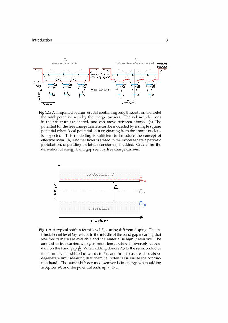
Fig 1.2: A typical shift in fermi-level EF during different doping. The in-trinsic Fermi level EF,i resides in the middle of the band gap meaning thatfew free carriers are available and the material is highly resistive. Theamount of free carriers n or p at room temperature is inversely depen-dant on the band gap 1
Eg. When adding donors Nd to the semiconductor
the fermi level is shifted upwards to EF,n and in this case reaches abovedegenerate limit meaning that chemical potential is inside the conduc-tion band. The same shift occurs downwards in energy when addingacceptors Na and the potential ends up at EF,p.
4 Introduction
1.1.2 DopingTo manipulate the placement of the chemical potential, thus changing the electricalproperties of the semiconductor, impurities are introduced effectively doping thecrystal, see Fig 1.2 [8]. Doping means that few atoms inside the crystal lattice ofa semiconductor is substituted with compatible atoms from another material tocreate an abundance (n-type) or absence (p-type) of electrons. Absence of electronscan be modelled as quasi-particles called holes, normally with higher effectivemass m∗ compared to electrons. Substituted atoms lending extra electrons arecalled donor states Na and respectively when removing electrons they are calledacceptor states Nd.
In this work a n-doping is used in the order of Nd ≈ 1018 cm−3, for comparisonthe concentration of atoms in a crystal is approximately 1/a3
≈ 1021 cm−3. III-Vcompounds, in many cases, have quite large lattice constant, small atom density,compared to Si which means that relatively small doping leads to degenerateFermi-level [9]. A semiconductor overview and comparison is given in Table 1.2.
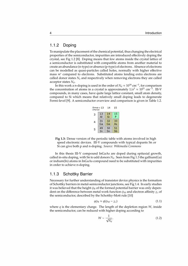
Fig 1.3: Dense version of the periodic table with atoms involved in highspeed electronic devices. III-V compounds with typical dopants Sn orSi can give both p and n-doping. Source: Wikimedia Commons
In this thesis III-V compound InGaAs are doped during epitaxial growth,called in-situ doping, with Sn to add donors Nd. Seen from Fig 1.3 the gallium(Ga)or indium(In) atoms in InGaAs compound need to be substituted with impuritiesin order to achieve n-doping.
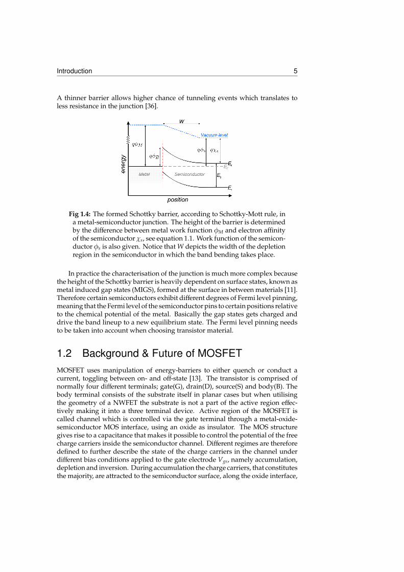
1.1.3 Schottky BarrierNecessary for further understanding of transistor device physics is the formationof Schottky barriers in metal-semiconductor junctions, see Fig 1.4. In early studiesit was believed that the height φB of the formed potential barrier was only depen-dent on the difference between metal work function φM and electron affinity χs ofthe semiconductor, described by the Schottky-Mott rule [10]
qφB ≈ q(φM − χs) (1.1)
where q is the elementary charge. The length of the depletion region W, insidethe semiconductor, can be reduced with higher doping according to
W ∼1√
Nd. (1.2)
Introduction 5
A thinner barrier allows higher chance of tunneling events which translates toless resistance in the junction [36].
Fig 1.4: The formed Schottky barrier, according to Schottky-Mott rule, ina metal-semiconductor junction. The height of the barrier is determinedby the difference between metal work function φM and electron affinityof the semiconductor χs, see equation 1.1. Work function of the semicon-ductor φs is also given. Notice that W depicts the width of the depletionregion in the semiconductor in which the band bending takes place.
In practice the characterisation of the junction is much more complex becausethe height of the Schottky barrier is heavily dependent on surface states, known asmetal induced gap states (MIGS), formed at the surface in between materials [11].Therefore certain semiconductors exhibit different degrees of Fermi level pinning,meaning that the Fermi level of the semiconductor pins to certain positions relativeto the chemical potential of the metal. Basically the gap states gets charged anddrive the band lineup to a new equilibrium state. The Fermi level pinning needsto be taken into account when choosing transistor material.
1.2 Background & Future of MOSFETMOSFET uses manipulation of energy-barriers to either quench or conduct acurrent, toggling between on- and off-state [13]. The transistor is comprised ofnormally four different terminals; gate(G), drain(D), source(S) and body(B). Thebody terminal consists of the substrate itself in planar cases but when utilisingthe geometry of a NWFET the substrate is not a part of the active region effec-tively making it into a three terminal device. Active region of the MOSFET iscalled channel which is controlled via the gate terminal through a metal-oxide-semiconductor MOS interface, using an oxide as insulator. The MOS structuregives rise to a capacitance that makes it possible to control the potential of the freecharge carriers inside the semiconductor channel. Different regimes are thereforedefined to further describe the state of the charge carriers in the channel underdifferent bias conditions applied to the gate electrode Vgs, namely accumulation,depletion and inversion. During accumulation the charge carriers, that constitutesthe majority, are attracted to the semiconductor surface, along the oxide interface,
6 Introduction
and in depletion these carriers are instead greatly reduced. When increasing thedegree of depletion, by modulating the gate bias above a certain threshold voltageVgs > Vt, new minority charge carriers are being generated effectively invertingthe channel, thus inversion is achieved.
Fig 1.5: Overview of how a MOSFET typically works. Depicting a planarn-transistor with no gate overlap (a) with the symbol describing a MOStransistor (b) in a circuit schematic. The schematic is used here to high-light relative position of terminals gate, drain and source in the banddiagrams. The band simulations shows both off- (c) and on-state (d).Below threshold voltage Vgs < Vt the biasing is insufficient for creatingan n-channel and the potential barrier quenches the thermionic emissionof electrons. Above threshold Vgs > Vt the charge carriers can move pastthe potential barrier.
At the two ends of the channel the source and drain terminals are situatedand used to control the electric field, by Vds, in the direction of the channel, hencecontrolling the passing current Ids. If there is an energy barrier present insidethe channel, due to difference in doping levels between channel and source/drainterminals, the current will not be able to flow from D- to S-terminal withoutexternal bias, called an enhancement mode device [14]. An example of a n-typeenhancement mode device is depicted in Fig 1.5, where accumulation of electronsinside the channel turns the device on [15].
Compared to other transistors the MOSFET offers low leakage current from thegate electrode due to the insulating oxide in the MOS interface [16]. Maintaininga low off-state leakage is key for reaching higher energy-efficiency in logical cir-cuits where the amount of transistors is correlated to increased processing power.Available field effect transistor without the metal-oxide-semiconductor interfaceis for example high-electron-mobility-transistor HEMT or metal-semiconductor-field-effect-transistor MESFET. A HEMT uses a wide bandgap material, as sub-stitute for a dielectric, between metal and channel which leads to good qualitysemiconductor interfaces sacrificing energy-efficiency for improved carrier trans-port properties [17]. These characteristics are beneficial for transistors used in RF
Introduction 7
applications.
1.2.1 Importance of High-κ Oxides
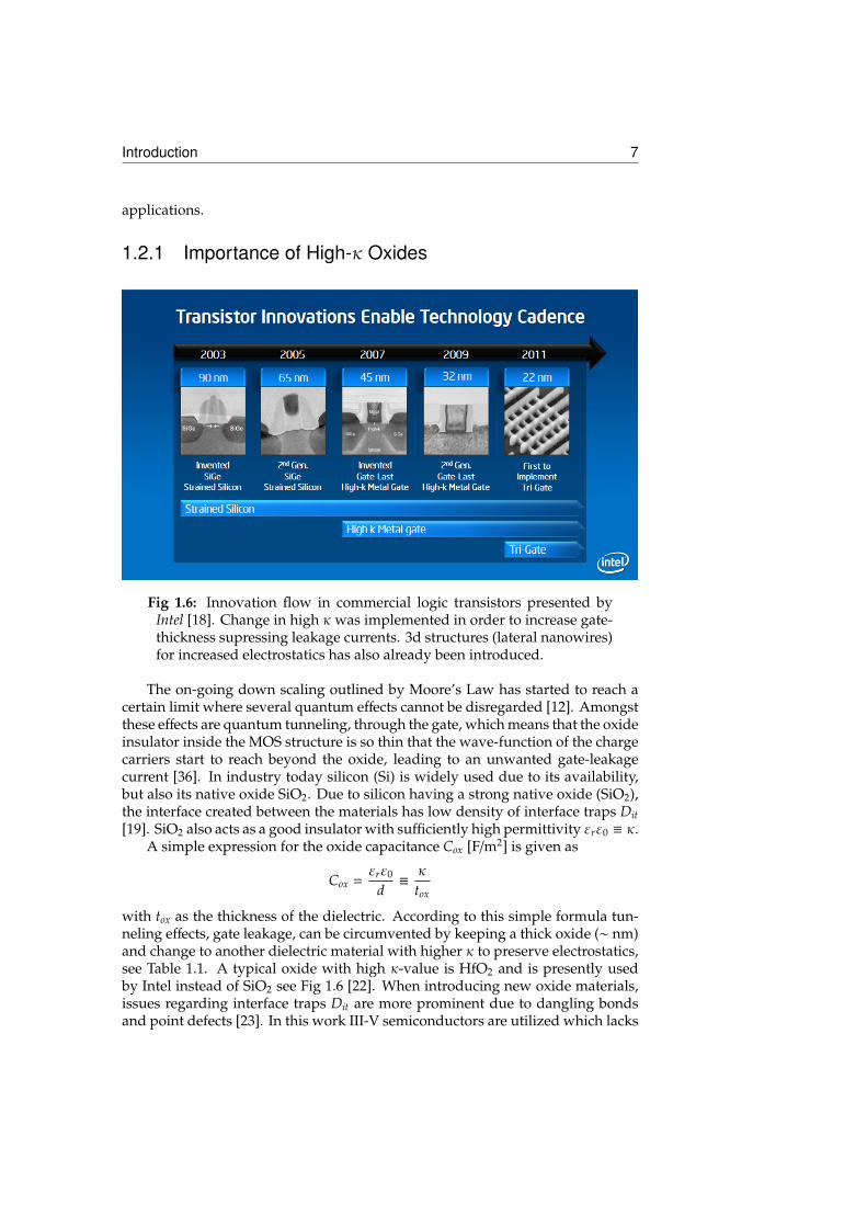
Fig 1.6: Innovation flow in commercial logic transistors presented byIntel [18]. Change in high κ was implemented in order to increase gate-thickness supressing leakage currents. 3d structures (lateral nanowires)for increased electrostatics has also already been introduced.
The on-going down scaling outlined by Moore’s Law has started to reach acertain limit where several quantum effects cannot be disregarded [12]. Amongstthese effects are quantum tunneling, through the gate, which means that the oxideinsulator inside the MOS structure is so thin that the wave-function of the chargecarriers start to reach beyond the oxide, leading to an unwanted gate-leakagecurrent [36]. In industry today silicon (Si) is widely used due to its availability,but also its native oxide SiO2. Due to silicon having a strong native oxide (SiO2),the interface created between the materials has low density of interface traps Dit[19]. SiO2 also acts as a good insulator with sufficiently high permittivity εrε0 ≡ κ.
A simple expression for the oxide capacitance Cox [F/m2] is given as
Cox =εrε0
d≡κtox
with tox as the thickness of the dielectric. According to this simple formula tun-neling effects, gate leakage, can be circumvented by keeping a thick oxide (∼ nm)and change to another dielectric material with higher κ to preserve electrostatics,see Table 1.1. A typical oxide with high κ-value is HfO2 and is presently usedby Intel instead of SiO2 see Fig 1.6 [22]. When introducing new oxide materials,issues regarding interface traps Dit are more prominent due to dangling bondsand point defects [23]. In this work III-V semiconductors are utilized which lacks
8 Introduction
good native oxides. Implementing a high-κ oxide on III-Vs can hence lead toinsufficient electrostatic control [20]. To minimize interface states, bi-layers canbe utilized with for example Al2O3 as a buffer layer between semiconductor andHfO2. Another source of Dit is doping of the semiconductor, where in-situ dopingcan degrade the crystal quality and therefore also the high-κ interface [21].
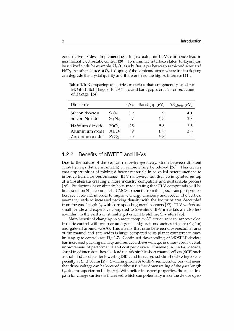
Table 1.1: Comparing dielectrics materials that are generally used forMOSFET. Both large offset ∆Ec,InAs and bandgap is crucial for reductionof leakage. [24]
Dielectric κ/ε0 Bandgap [eV] ∆Ec,InAs [eV]
Silicon dioxide SiO2 3.9 9 4.1Silicon Nitride Si3N4 7 5.3 2.7
Hafnium dioxide HfO2 25 5.8 2.5Aluminium oxide Al2O3 9 8.8 3.6Zirconium oxide ZrO2 25 5.8 -
1.2.2 Benefits of NWFET and III-VsDue to the nature of the vertical nanowire geometry, strain between differentcrystal planes (lattice mismatch) can more easily be relaxed [26]. This createsvast opportunities of mixing different materials in so called heterojunctions toimprove transistor performance. III-V nanowires can thus be integrated on topof a Si-substrate creating a more industry compatible and sustainable process[28]. Predictions have already been made stating that III-V compounds will beintegrated on Si in commercial CMOS to benefit from the good transport proper-ties, see Table 1.2, in order to improve energy efficiency and speed. The verticalgeometry leads to increased packing density with the footprint area decoupledfrom the gate length Lg with corresponding metal contacts [27]. III-V wafers aresmall, brittle and expensive compared to Si-wafers, III-V materials are also lessabundant in the earths crust making it crucial to still use Si-wafers [25].
Main benefit of changing to a more complex 3D structure is to improve elec-trostatic control with wrap-around gate configurations such as tri-gate (Fig 1.6)and gate-all around (GAA). This means that ratio between cross-sectional areaof the channel and gate width is large, compared to its planar counterpart, max-imizing gate control, see Fig 1.7. Continued downscaling of MOSFET deviceshas increased packing density and reduced drive voltage, in other words overallimprovement of performance and cost per device. However, in the last decade,shrinking dimensions has also lead to undesirable short channel effects (SCE) suchas drain induced barrier lowering DIBL and increased subthreshold swing SS, es-pecially at Lg ≤ 30 nm [29]. Switching from Si to III-V semiconductors will meanthat drive voltage can be lowered without further downscaling of the gate lengthLg, due to superior mobility [30]. With better transport properties, the mean freepath for charge carriers is increased which can potentially make the device oper-
Introduction 9
Fig 1.7: Cross-sectional illustration of different gate geometries includingplanar, tri-gate and gate-all-around (GAA). (a) Side view of the conven-tional planar layout creating a sandwich of layers. (b) 3d implementationof lateral nanowires by tri-gate leading to better gate coverage, thus in-creased electrostatics compared to planar. (c) Complete overview of aGAA geometry, created with vertical nanowires, where ratio betweengate width and cross-sectional channel area is maximized optimizingelectrostatic control.
ate in the ballistic regime, with no scattering events occuring inside the channel.Intel has already improved transport properties (∼ 70%) by implementation ofstrained silicon as channel material, see Fig 1.6 [31].
Table 1.2 shows material parameters for selected semiconductors. III-V com-pounds has in several cases better mobility µn compared to silicon (Si), but this isnot the case for hole mobility µp. Having overall good performance for both holesand electrons is necessary for CMOS implementation in logic circuits. In this workhowever the processed MOSFET devices will be optimised for high frequency RFapplication, meaning that electron mobility (n-doping) is of importance. Observethat there is a fundamental correlation between lattice constant a0 and bandgapEg as a0 ∼ 1/Eg. Implementing materials with a small bandgap might seem bene-ficial due to high mobility, but will lead to sensitivity such as thermal instabilityand low breakdown voltage. Notice that Si suffers from indirect bandgap whichdegrades the effective mass. Therefore III-V materials has been the first choice foroptoelectronic devices, such as light-emitting-diode LED [32]. The currents arenecessarily not higher in a MOSFET utilizing a high mobility III-V compound dueto larger crystal lattice constant a0, which translates to reduced density of states.The main benefit is that the ballistic regime, with no scattering inside the channel,can be reached at larger gate lengths (Lg ≤ 30 nm) due to longer mean free path.The performance of a ballistic transistor is dependent on the injection velocity vinjof the charge carriers, which scales inversely with effective mass vinj ∼ 1/m∗ [33].
10 Introduction
Table 1.2: Outlining important material parameters for selected IV andIII-V semiconductors. Superior transport µn is shown for the III-V com-pounds compared to silicon. Parameters taken from [37]. Notice thatthe injection velocity for electrons vinj,e is extracted from virtual sourcemodelling with Lg = 30nm [34].
Semi µn µp Eg a0 m∗/me vinj,e-conductor [cm2/Vs] [cm2/Vs] [eV] [Å] [cm/s]
Si 1400 450 1.12 5.43 0.36 1.2·107
Ge 3900 1900 0.66 5.66 0.22
GaAs 8500 400 1.42 5.65 0.063InAs 40000 500 0.354 6.06 0.023 3.7·107
In0.53Ga0.47As 12000 300 0.74 5.87 0.041 2.8·107
InSb 77000 850 0.17 6.48 0.014GaSb 3000 1000 0.73 6.10 0.041
1.2.3 Design of RF Transistors
Radio frequency (RF) transistors are designed to handle high frequencies, wellabove 100 GHz, and still maintain both current and power gain. Emphasis is alsoput on the transistors ability to showcase high breakdown and stable saturationof the output conductance gd. Further discussion of important metrics for highfrequency performance are given in Chapter 2. Breakdown is the ability of thedevice to handle large currents during significant voltage bias (Vds ≥ 4 V) and isquantified by the destructive breakdown voltage VB at which the device physicallybreaks.
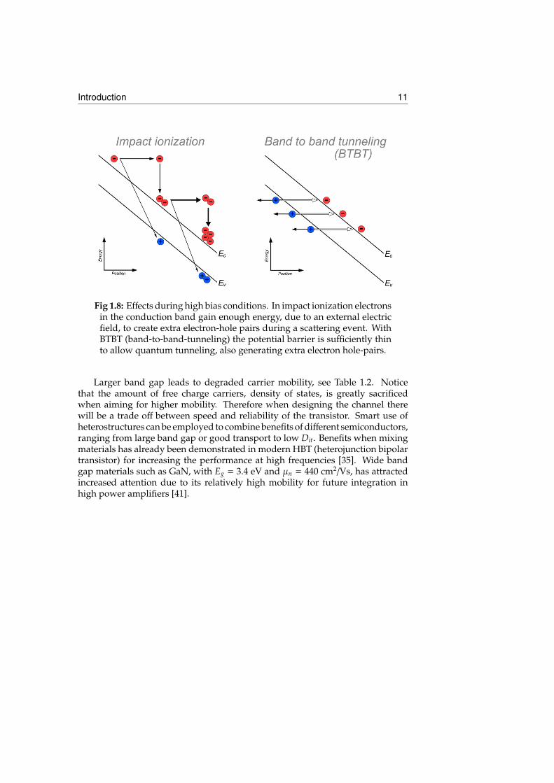
Effects leading to poor saturation and low VB, when disregarding short chan-nel effects (SCE), are impact ionization and band-to-band tunneling (BTBT), seeFig 1.8. Both effects are inversely dependent on the band gap, ∼ 1/Eg, of the ac-tive material that constitutes the MOSFET channel area [39, 42]. Impact ionizationoccurs when the kinetic energy of the charge carriers surpass the energy neededfor excitation of extra electrons over the band gap. Thus when energy is lostvia scattering events the probability of creating new electron-hole pairs is high[40]. This leads to a chain of events where the amount of free charge carriers aregreatly accelerated. In a MOSFET impact ionization effects will lead to a suddenincrease of the output current that can damage and ultimately lead to destructivebreakdown of the device. The band-to-band tunneling effect, on the other hand,is dependent on the distortion of the potential seen by the charge carriers. Whenthe potential barrier shrinks, under certain bias conditions, quantum tunnelingis enabled through the band gap itself and new electron-hole-pairs can be gener-ated [36]. These different effects likely occur if the provided energy, by a certainvoltage drop Vbias, is significantly larger than the band gap, qVbias >> Eg with q asthe elementary charge, inside a segment of the channel material.
Introduction 11
Fig 1.8: Effects during high bias conditions. In impact ionization electronsin the conduction band gain enough energy, due to an external electricfield, to create extra electron-hole pairs during a scattering event. WithBTBT (band-to-band-tunneling) the potential barrier is sufficiently thinto allow quantum tunneling, also generating extra electron hole-pairs.
Larger band gap leads to degraded carrier mobility, see Table 1.2. Noticethat the amount of free charge carriers, density of states, is greatly sacrificedwhen aiming for higher mobility. Therefore when designing the channel therewill be a trade off between speed and reliability of the transistor. Smart use ofheterostructures can be employed to combine benefits of different semiconductors,ranging from large band gap or good transport to low Dit. Benefits when mixingmaterials has already been demonstrated in modern HBT (heterojunction bipolartransistor) for increasing the performance at high frequencies [35]. Wide bandgap materials such as GaN, with Eg = 3.4 eV and µn = 440 cm2/Vs, has attractedincreased attention due to its relatively high mobility for future integration inhigh power amplifiers [41].

12 Introduction
Chapter2MOSFET Performance Metrics
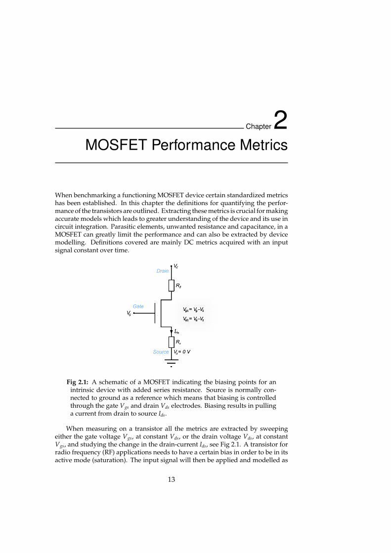
When benchmarking a functioning MOSFET device certain standardized metricshas been established. In this chapter the definitions for quantifying the perfor-mance of the transistors are outlined. Extracting these metrics is crucial for makingaccurate models which leads to greater understanding of the device and its use incircuit integration. Parasitic elements, unwanted resistance and capacitance, in aMOSFET can greatly limit the performance and can also be extracted by devicemodelling. Definitions covered are mainly DC metrics acquired with an inputsignal constant over time.
Fig 2.1: A schematic of a MOSFET indicating the biasing points for anintrinsic device with added series resistance. Source is normally con-nected to ground as a reference which means that biasing is controlledthrough the gate Vgs and drain Vds electrodes. Biasing results in pullinga current from drain to source Ids.
When measuring on a transistor all the metrics are extracted by sweepingeither the gate voltage Vgs, at constant Vds, or the drain voltage Vds, at constantVgs, and studying the change in the drain-current Ids, see Fig 2.1. A transistor forradio frequency (RF) applications needs to have a certain bias in order to be in itsactive mode (saturation). The input signal will then be applied and modelled as
13
14 MOSFET Performance Metrics
a small signal shift of the voltage. To evaluate the small signal response differentparameters describing the shapes of the DC curves are defined.
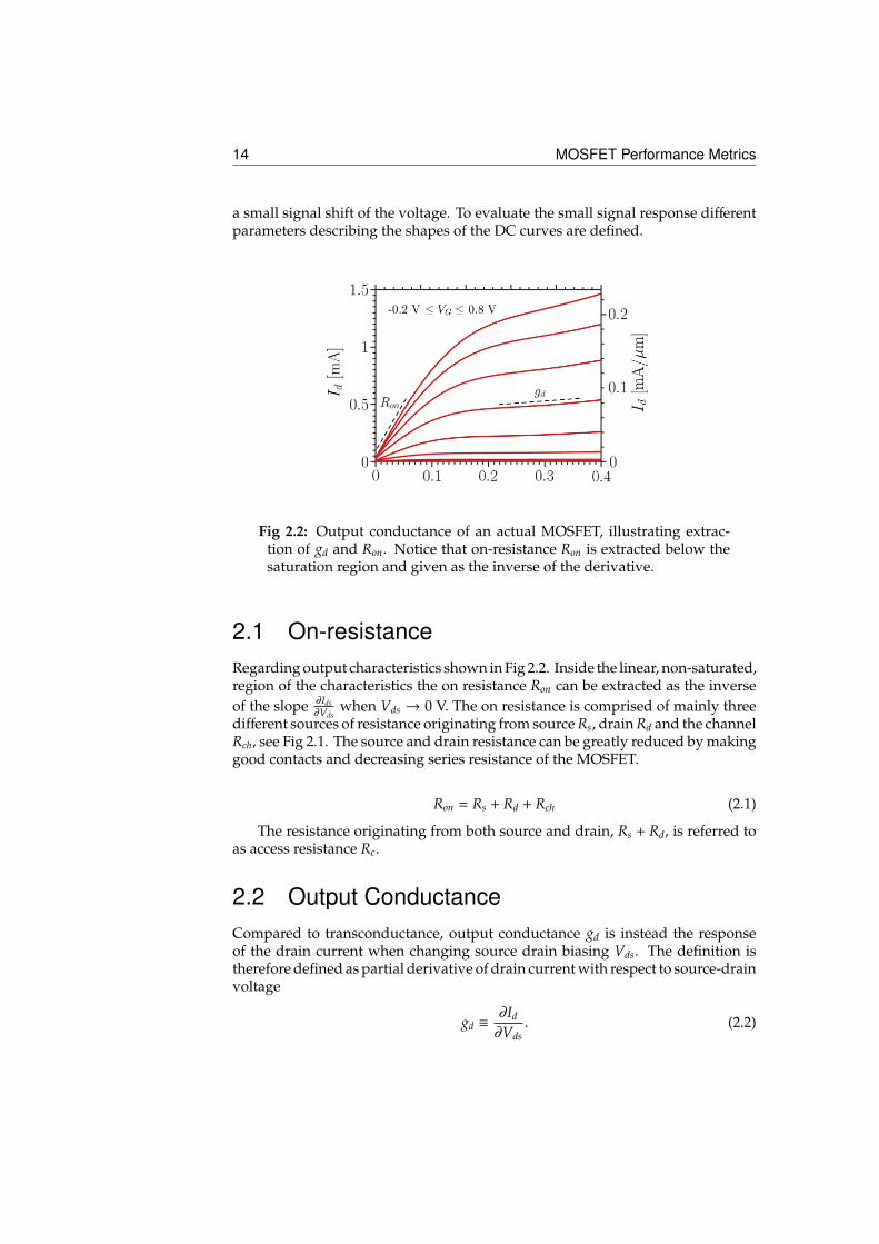
Fig 2.2: Output conductance of an actual MOSFET, illustrating extrac-tion of gd and Ron. Notice that on-resistance Ron is extracted below thesaturation region and given as the inverse of the derivative.
2.1 On-resistanceRegarding output characteristics shown in Fig 2.2. Inside the linear, non-saturated,region of the characteristics the on resistance Ron can be extracted as the inverseof the slope ∂Ids
∂Vdswhen Vds → 0 V. The on resistance is comprised of mainly three
different sources of resistance originating from source Rs, drain Rd and the channelRch, see Fig 2.1. The source and drain resistance can be greatly reduced by makinggood contacts and decreasing series resistance of the MOSFET.
Ron = Rs + Rd + Rch (2.1)
The resistance originating from both source and drain, Rs + Rd, is referred toas access resistance Rc.
2.2 Output ConductanceCompared to transconductance, output conductance gd is instead the responseof the drain current when changing source drain biasing Vds. The definition istherefore defined as partial derivative of drain current with respect to source-drainvoltage
gd ≡∂Id
∂Vds. (2.2)
MOSFET Performance Metrics 15
Fig 2.3: A typical example of transfer characteristics for an enhancementmode MOSFET, in linear (a) and logarithmic scale (b). Example extractedfrom an actual measured transistor. gm represents the derivative of theId-Vds characteristics. Vt extrapolation carried out with the tangent ofthe voltage that yields maximum gm. SS is given by the slope of theexponentially increasing sub-threshold, Vgs < Vt, segment. Ion is definedas one drive voltage Vdd = 0.5V above a fixed Io f f current of 100 nA/µm
An ideal MOSFET has zero gd in saturation, meaning that channel lengthmodulation has no effect on the resistance of the active area.
2.3 TransconductanceA transistor metric important for transistor in RF application is transconductancegm, defined as the partial derivative of the drain current with respect to gatevoltage
gm ≡∂Id
∂Vgs. (2.3)
When applying a small signal input at the gate electrode the given responseat the drain current is quantified by this metric.
2.4 Threshold VoltageAt a certain threshold voltage Vt the transistor switches from ON to OFF-state,see Fig 1.5. Typically defined as the gate voltage needed to initiate inversion ofthe channel. To register the threshold voltage via the Ids-Vgs curve the tangentfrom the Vgs point, corresponding to the peak value of transconductance gm,max,is extrapolated down to zero drain current, see Fig 2.3. The threshold voltage isin reality not well defined which makes extraction of this metric quite arbitrary.
16 MOSFET Performance Metrics
2.5 Voltage GainWith transconductance gm and output conductance gd given the small signalvoltage gain of the transistor, in CS configuration, can be derived from
Av =∂Vds
∂Vgs=
gm
gd. (2.4)
Notice that the given voltage gain Av is for a transistor in open circuit config-uration.
2.6 Subthreshold SwingThermionic emission will always be limited by the amount of available free car-riers above a certain potential barrier. When heat is applied to a system thecarriers are redistributed according to Fermi-distribution. At high enough tem-perature, such as room temperature (∼ 300 K), the distribution can be referred toas a Fermi-tail (similar to Boltzmann distribution) that is decaying exponentiallywhen moving to higher energies compared to the conduction band, see Fig 1.2.The theoretical limit is hence naturally dependent on the distribution describedby the Fermi-function and referred to as subthreshold slope
SS = −1
log10(e)kBT
q. (2.5)
q represents the elementary charge, kB boltzmanns constant and e Euler’s number.SS is identified from the transfer characteristics, in logarithmic scale, as the linearincrease in the sub-threshold region, see Fig 2.3.
For logic circuits SS is an essential parameter since a logic device is systemati-cally switched between ON and OFF-state. In other words SS describes how wella MOSFET works as a relay switch.
2.7 Cut-off FrequencyThe only AC-metric covered in this chapter, quantifying at what frequency ft ofthe input signal, applied to the gate, the MOSFET showcases gain. Mentioned tounderline the importance of gm and is described as
ft ≈gm,i
2π(Cgd + Cgs)(2.6)
with intrinsic transconductance gm,i. Notice that extrinsic capacitances are ap-proximated as the dominant source of parasitics and also access resistance, Rs &Rd, are disregarded. In other words the ft scales linearly with gm.
Chapter3MOSFET Evolution
Fig 3.1: a) The conventional "drain last" process developed by Sofia Jo-hansson. b) Comparison done with self aligned gate process, "drainfirst", outlined by Martin Berg [46, 47]. Schematic used, with permission,from doctoral thesis by Martin Berg.
The process used for manufacturing vertical nanowire MOSFET in this thesiswas developed by Martin Berg and Karl-Magnus Persson [47]. Vertical processingrequire high precision tools optimized for an all new direction, namely normalto the substrate. Since lateral processing is utilized in industry and refined formore than half a century switching to vertical is challenging [43]. This typeof processing is still in its cradle and is facing some of the challenges that waseventually resolved for the planar architecture. However vertical processing isfundamentally different from lateral due to the device being built from bottom tothe top in a "bottom-up" fashion. In the bottom-up approach a system is piecedtogether to add up to a bigger and more complex system.
Previous processes optimized for RF-performance has included sub-sequentiallyadding all the pieces from bottom to the top. Starting with a wafer containingnanowires a first spacer is deposited followed by a gate and afterwards the second
17
18 MOSFET Evolution
spacer is added followed by the top contact. This method of conventionally de-positing the top contact last was spearheaded by Sofia Johansson who developedvertical transistor that showcased gain at high frequency input, ft = 140 GHz, seeFigure 3.1 [44]. In this thesis however the process starts with deposition of the topcontact which enables a self-aligned gate process and also lends more margins inthe high precision alignment steps.
A self-aligned process is crucial for increased performance due to completegate coverage of the channel which enables lower series resistance. With largercurrents, high amplification gm is possible which is fundamental for high RF-performance. The downside of tighter dimensions is larger parasitic which putsmore emphasis on low-κ integration, possibly with the use of air spacers.
Fig 3.2: Showing the benefits, by band-structure simulation, of incorpo-rating InGaAs [50]. Schematic used, with permission, from doctoral thesis byJun Wu.
The first generation of the gate last process consisted of pure InAs nanowiresto accommodate both the digital and RF domain, see Fig 3.1. Growth techniqueswhere adapted to decrease the resistance of the wire including a highly doped InAsovergrowth creating a shell for good ohmic contact. In later steps the shell couldbe selectively etched revealing the intrinsic or lowly doped gate area for high-κand metal deposition. The first generation transistors showcased instability, withhigh output conductance gd and low breakdown, due to the narrow bandgap ofInAs.
In the second generation of NWFET these issues where addressed by incor-porating a heterostructure featuring InAs and InGaAs, see Figure 3.2. Where thecomposition of the nanowire is gradually changed from InAs to InGaAs whenmoving from bottom to the top [49]. The overgrown shell, in this case, con-sisted of highly doped InGaAs. The result of this update in the NWFET remainsunpublished.
Parallel to the second generation of devices a test is carried out, in this thesis,where the heterostructure is inverted, see Fig 3.3. Instead of gradually grad-ing from InAs to InGaAs, the InGaAs is abruptly incorporated in the bottom
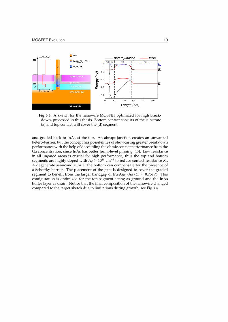
MOSFET Evolution 19
Fig 3.3: A sketch for the nanowire MOSFET optimized for high break-down, processed in this thesis. Bottom contact consists of the substrate(a) and top contact will cover the (d) segment.
and graded back to InAs at the top. An abrupt junction creates an unwantedhetero-barrier, but the concept has possibilities of showcasing greater breakdownperformance with the help of decoupling the ohmic contact performance from theGa concentration, since InAs has better fermi-level pinning [45]. Low resistancein all ungated areas is crucial for high performance, thus the top and bottomsegments are highly doped with Nd ≥ 1018 cm−3 to reduce contact resistance Rc.A degenerate semiconductor at the bottom can compensate for the presence ofa Schottky barrier. The placement of the gate is designed to cover the gradedsegment to benefit from the larger bandgap of In0.5Ga0.5As (Eg ≈ 0.75eV). Thisconfiguration is optimized for the top segment acting as ground and the InAsbuffer layer as drain. Notice that the final composition of the nanowire changedcompared to the target sketch due to limitations during growth, see Fig 3.4
20 MOSFET Evolution
Fig 3.4: A sketch for composition of the nanowires processed in this thesis.Due to limitations and variations during growth there is a differencebetween the target composition and final batch.
Chapter4MOSFET Fabrication
Fig 4.1: An overview of the finished transistor in top ground configu-ration. The structure can also be bottom grounded meaning that thesource and drain contacts, in this case, are switched. The choice of theoptimal configuration, top ground, is motivated by band-simulations,see Fig 3.3.
The fabrication of the vertical MOSFET is a complex and involves many stepsin order to deposit the top metal first for creating sufficient gate-overlap and,in the end, realize the final structure, see Fig 4.1. All the steps are thoroughlycovered, in this chapter, combined with theory needed for greater understandingof process sensitivity.
21
22 MOSFET Fabrication
4.1 Nanowire Growth
Fig 4.2: High resolution SEM images of the grown nanowires. Goldparticle diameter defined by EBL is 28 nm. (a) A full set of double rowarrays with internal spacing of 200 nm. (b) Zoom in of a few nanowiresin the array to highlight the smooth surface which indicates good crystalquality.
The device performance will always be limited by the quality of the nanowiresmaking up the final transistor. The growth of the nanowires was therefore out-sourced to an experienced researcher, namely Dr. Johannes Svensson at EITdepartment, Lund University. Therefore the growth process is described mostlyqualitatively.
To alleviate lattice stress and enable growth of good quality III-V nanowires, ontop of a silicon substrate, a 260 nm thick InAs layer is grown by metal organic vaporphase epitaxy MOVPE. In this epitaxy technique the sample is placed inside achamber and flooded with precursor gases (TMIn, AsH3), at elevated temperature,which reacts on top of the substrate surface to form the final crystalline InAs bufferlayer. The silicon substrate, now covered with InAs, is later patterned with golddots by an EBL defined lift off process using a PMMA film. The gold dots willact as catalysts in the vapor-liquid-solid (VLS) process. In this mechanism, thecatalyst dots create liquid alloy droplets at high temperature (420o C-470o C) byadsorbing the vapors inside the MOVPE chamber [51]. Thus local supersaturationof the alloy occurs, which means that the concentration of components exceed itsequilibrium. The system then strives to lower its energy which in turn enables 1Dgrowth that continues as long as precursor gases are supplied, creating nanowires.By controlling the supply of precursor gases (TMIn, AsH3, TMGa), during theprocess, InGaAs composition of the nanowire can be controlled along the growthdirection [49].
Different patterns are defined by the EBL process including double row arrays,pads and single nanowire structures. The growth is thus optimized for the most
MOSFET Fabrication 23
reoccuring structure, namely the zigzag double row array, see Fig 4.2.Doping of the wires are carried out in-situ, meaning that they are doped in
conjunction with deposition [52]. The dopants are added by another precursorgas, namely TESn, which adds n-doping by substitution with Sn atoms. The pre-cision of the in-situ doping is limited by diffusion mechanisms leading to dopantatoms relocating and spreading at elevated temperatures to reduce induced strain.These effects amounted to a slightly different outcome in doping concentrationand length in the final batch compared to target composition, see Fig 3.4.
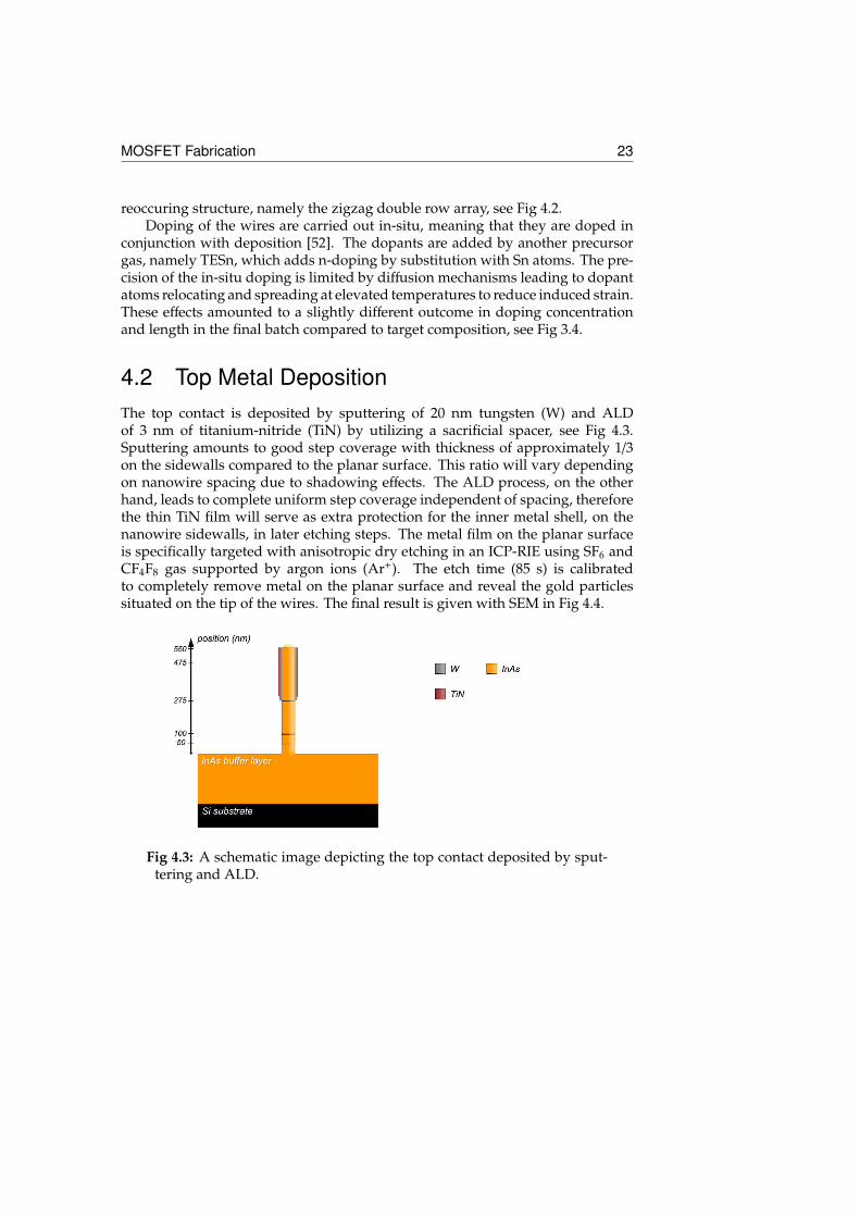
4.2 Top Metal DepositionThe top contact is deposited by sputtering of 20 nm tungsten (W) and ALDof 3 nm of titanium-nitride (TiN) by utilizing a sacrificial spacer, see Fig 4.3.Sputtering amounts to good step coverage with thickness of approximately 1/3on the sidewalls compared to the planar surface. This ratio will vary dependingon nanowire spacing due to shadowing effects. The ALD process, on the otherhand, leads to complete uniform step coverage independent of spacing, thereforethe thin TiN film will serve as extra protection for the inner metal shell, on thenanowire sidewalls, in later etching steps. The metal film on the planar surfaceis specifically targeted with anisotropic dry etching in an ICP-RIE using SF6 andCF4F8 gas supported by argon ions (Ar+). The etch time (85 s) is calibratedto completely remove metal on the planar surface and reveal the gold particlessituated on the tip of the wires. The final result is given with SEM in Fig 4.4.
Fig 4.3: A schematic image depicting the top contact deposited by sput-tering and ALD.
24 MOSFET Fabrication
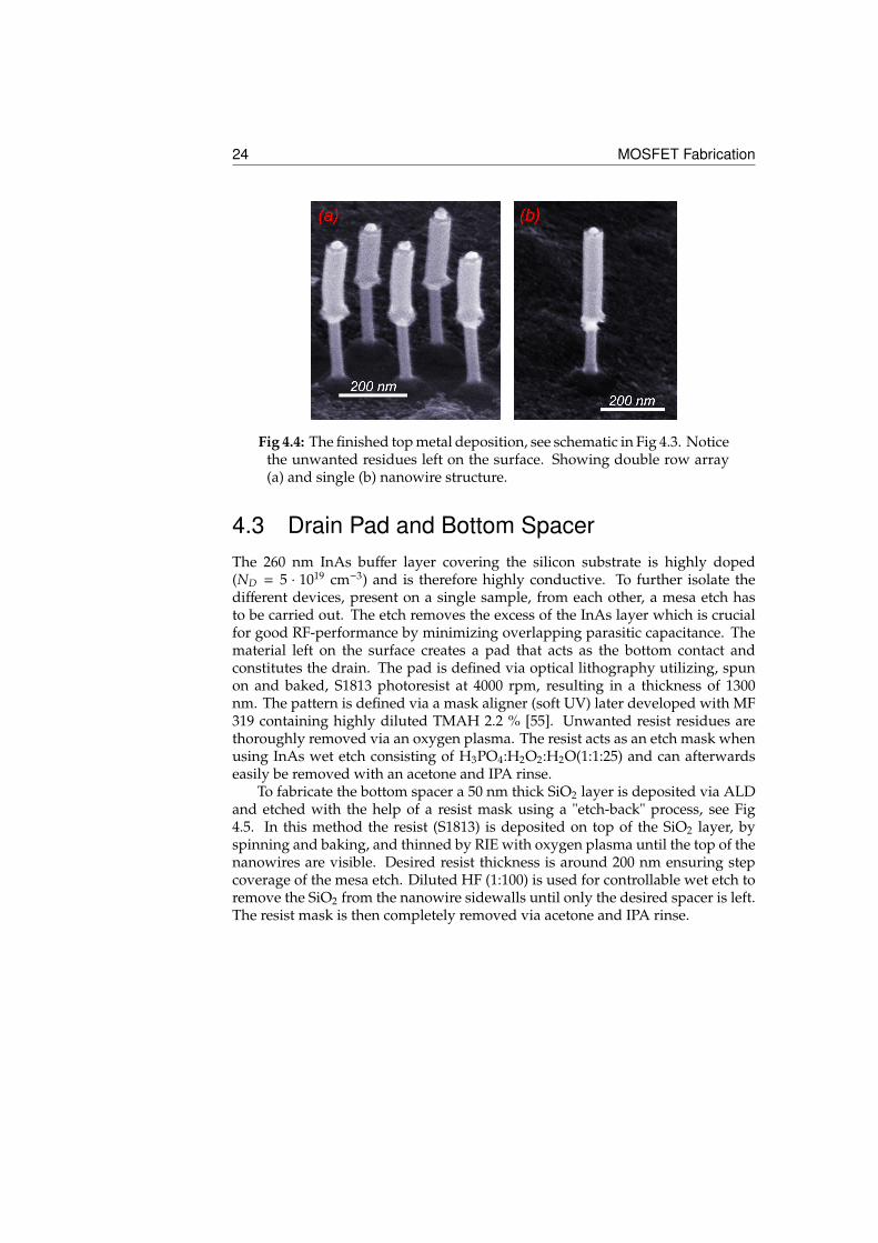
Fig 4.4: The finished top metal deposition, see schematic in Fig 4.3. Noticethe unwanted residues left on the surface. Showing double row array(a) and single (b) nanowire structure.
4.3 Drain Pad and Bottom SpacerThe 260 nm InAs buffer layer covering the silicon substrate is highly doped(ND = 5 · 1019 cm−3) and is therefore highly conductive. To further isolate thedifferent devices, present on a single sample, from each other, a mesa etch hasto be carried out. The etch removes the excess of the InAs layer which is crucialfor good RF-performance by minimizing overlapping parasitic capacitance. Thematerial left on the surface creates a pad that acts as the bottom contact andconstitutes the drain. The pad is defined via optical lithography utilizing, spunon and baked, S1813 photoresist at 4000 rpm, resulting in a thickness of 1300nm. The pattern is defined via a mask aligner (soft UV) later developed with MF319 containing highly diluted TMAH 2.2 % [55]. Unwanted resist residues arethoroughly removed via an oxygen plasma. The resist acts as an etch mask whenusing InAs wet etch consisting of H3PO4:H2O2:H2O(1:1:25) and can afterwardseasily be removed with an acetone and IPA rinse.
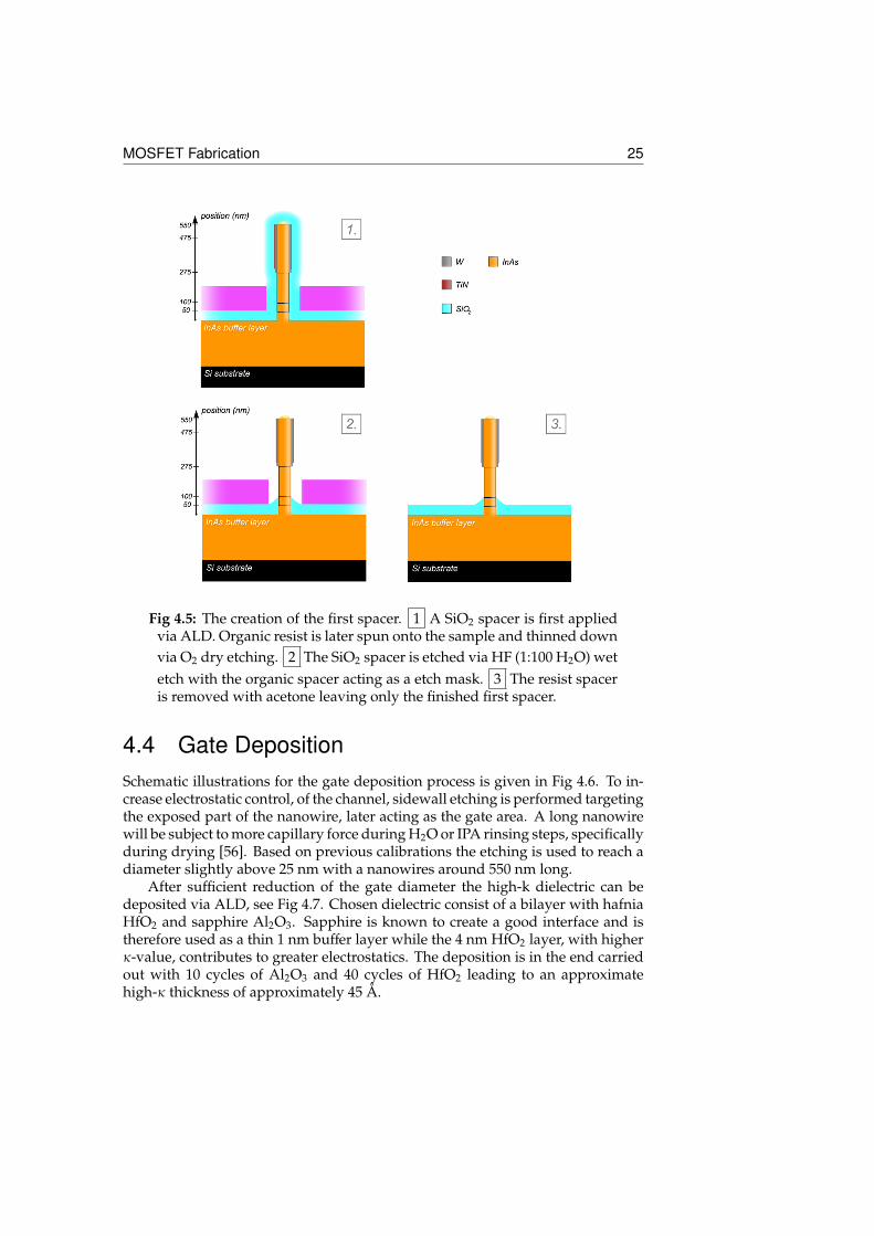
To fabricate the bottom spacer a 50 nm thick SiO2 layer is deposited via ALDand etched with the help of a resist mask using a "etch-back" process, see Fig4.5. In this method the resist (S1813) is deposited on top of the SiO2 layer, byspinning and baking, and thinned by RIE with oxygen plasma until the top of thenanowires are visible. Desired resist thickness is around 200 nm ensuring stepcoverage of the mesa etch. Diluted HF (1:100) is used for controllable wet etch toremove the SiO2 from the nanowire sidewalls until only the desired spacer is left.The resist mask is then completely removed via acetone and IPA rinse.
MOSFET Fabrication 25
Fig 4.5: The creation of the first spacer. 1 A SiO2 spacer is first appliedvia ALD. Organic resist is later spun onto the sample and thinned downvia O2 dry etching. 2 The SiO2 spacer is etched via HF (1:100 H2O) wetetch with the organic spacer acting as a etch mask. 3 The resist spaceris removed with acetone leaving only the finished first spacer.
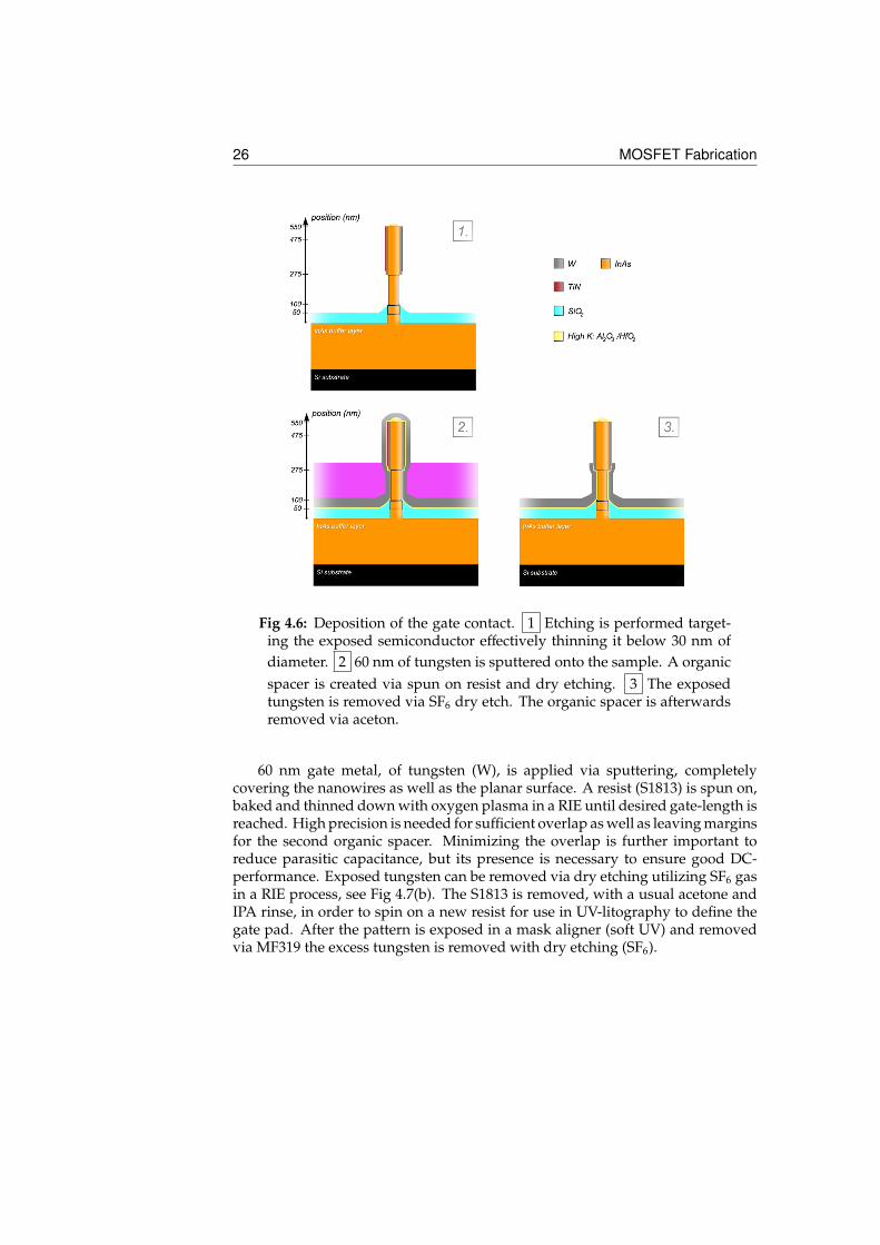
4.4 Gate DepositionSchematic illustrations for the gate deposition process is given in Fig 4.6. To in-crease electrostatic control, of the channel, sidewall etching is performed targetingthe exposed part of the nanowire, later acting as the gate area. A long nanowirewill be subject to more capillary force during H2O or IPA rinsing steps, specificallyduring drying [56]. Based on previous calibrations the etching is used to reach adiameter slightly above 25 nm with a nanowires around 550 nm long.
After sufficient reduction of the gate diameter the high-k dielectric can bedeposited via ALD, see Fig 4.7. Chosen dielectric consist of a bilayer with hafniaHfO2 and sapphire Al2O3. Sapphire is known to create a good interface and istherefore used as a thin 1 nm buffer layer while the 4 nm HfO2 layer, with higherκ-value, contributes to greater electrostatics. The deposition is in the end carriedout with 10 cycles of Al2O3 and 40 cycles of HfO2 leading to an approximatehigh-κ thickness of approximately 45 Å.
26 MOSFET Fabrication
Fig 4.6: Deposition of the gate contact. 1 Etching is performed target-ing the exposed semiconductor effectively thinning it below 30 nm ofdiameter. 2 60 nm of tungsten is sputtered onto the sample. A organicspacer is created via spun on resist and dry etching. 3 The exposedtungsten is removed via SF6 dry etch. The organic spacer is afterwardsremoved via aceton.
60 nm gate metal, of tungsten (W), is applied via sputtering, completelycovering the nanowires as well as the planar surface. A resist (S1813) is spun on,baked and thinned down with oxygen plasma in a RIE until desired gate-length isreached. High precision is needed for sufficient overlap as well as leaving marginsfor the second organic spacer. Minimizing the overlap is further important toreduce parasitic capacitance, but its presence is necessary to ensure good DC-performance. Exposed tungsten can be removed via dry etching utilizing SF6 gasin a RIE process, see Fig 4.7(b). The S1813 is removed, with a usual acetone andIPA rinse, in order to spin on a new resist for use in UV-litography to define thegate pad. After the pattern is exposed in a mask aligner (soft UV) and removedvia MF319 the excess tungsten is removed with dry etching (SF6).
MOSFET Fabrication 27
Fig 4.7: The result of the gate length definition. Showing a double rowarray (a) after high-κ deposition and (b) post gate etch.
4.5 Via Holes and Top ContactA second organic spacer is fabricated with spun on S1813, now permanentlybaked and thinned down until 50-100 nm of the top metal is visible, see Fig 4.8.To enable metal-to-metal connection of the top contact the high-κ is removed witha BOE (HF) wet etch. All terminals must further be available for connection viathe top metal, thus via holes for both the gate and drain has to be etched. A resistetch mask (S1813) is spun on and baked, and via holes are exposed, one at a time,with mask alignment (soft UV) and development. The gate via is completelycleaned out with oxygen plasma, locally removing the organic spacer, in a RIE.The drain via is also cleaned out with a oxygen plasma followed by a BOE etch forhigh-κ and bottom spacer removal. Sputtering is used to deposit the top contactconsisting of 15 nm nickel (Ni), 30 nm tungsten (W) and 200 nm gold (Au). Withthe tungsten acting as a diffusion barrier and Ni for creating a good metal-to-metalinterface.
The top metal layout, shown in Fig 4.9, is designed to isolate the gate, sourceand drain terminals from each other and is defined with a UV patterned re-sist (S1813) mask followed by three individual etch steps. The gold is wetetched using potassium-iodine (KI), the tungsten via SF6 dry etching and Niwith H2O:H2SO4:HNO3:CH3COOH (10:5:5:2) wet etching.
28 MOSFET Fabrication
Fig 4.8: Deposition of the second spacer and top contact. 1 An organicspacer is spun onto the sample, permanently baked and thinned downvia O2 dry etching. 2 Via holes are etched with sacrificial resist layeracting as etch mask where via holes are exposed, one at a time, via UVlitography. 3 Top contact is sputtered consisting of Ni, W and Au.
Fig 4.9: Showing the finished top metal layout in top grounded configu-ration.
Chapter5Result & Analysis
Two batches were finalized during this diploma work, with each batch containingtwo full-scale samples. The first processed batch only resulted in one device withtransistor DC-characteristics and the second one showcased promising resultswith a high yield of approximately 20, of 110 in total, working transistors on eachsample. Techniques for RF-optimization were not employed, such as minimiz-ing overlap capacitance with finger contacts, thus only DC-characteristics weremeasured. To further reach sufficient results with high RF-performance, the gm iscrucial and scales linearly with cut off frequency ft (equation 2.6), but also highbreakdown (Vds ≥ 4 V) is essential as proof-of-concept. The measurements of thedevices were carried out in a probe station.
5.1 ProcessingThis section serves to highlight differences between the processed samples andalso discuss challenges during certain processing steps. Many of the used ma-chines such as the ICP-RIE and RIE are not dedicated for a certain set of materials.Thus the chambers are constantly contaminated with many different substancesduring their life cycles. For this process it has meant that the etch rates were con-stantly varying which required extra caution and frequent SEM inspections. Bearin mind that many machines are not optimized for vertical processing making iteven more tedious when high precision alignment is required.
Chamber conditions and bad calibration of the anisotropic dry etching stepsled to the first batch showcasing extra roughness of the fabricated top contact.In many instances the gold particle was completely etched away including thesemiconductor material underneath leaving a hollow top metal contact, see Fig5.1(a). The majority of devices where therefore completely destroyed during themany processing steps ahead. Fig 5.2 shows the severity of damage to one of thefew surviving double row arrays.
During the second batch the ICP-RIE was correctly calibrated but the chamberwas not sufficiently cleaned. A residual film was therefore left on the surface afteranisotropic etching and removal of the HSQ spacer, see Fig 5.1(b). The originand composition of the film could not be confirmed due to the lack of propertools for analysis. Sample B, in the second batch, was heavily damaged by the
29
30 Result & Analysis
residual film and therefore extra wet etching steps where tested for removing thefilm. The sample was, after top metal fabrication, put in extended BOE(HF) etchfollowed by hydrogen passivation in H2SO4, both steps had limited effect andmostly etched the exposed nanowire sidewalls. Sample A was also covered by theresidual film but to less extent so no extra etching steps were performed. Noticethat many nanowire arrays, especially in Sample B, were completely collapsedafter the top contact fabrication. Most likely due to residues ripping away fromthe planar surface during the HSQ removal. In contrast to the first batch thequality of the top contact was greatly improved for batch #2. A fair comparisonbetween the top contacts of single nanowire structures are performed in Fig 5.1.
Extra caution for further collapse had to be taken during the targeted sidewalletching. Therefore etching was only performed on Sample A and not on Sample B.Therefore the diameter was significantly smaller on Sample A potentially leading tobetter electrostatic control of the gate. The difference is given in Fig 5.3 showingnanowire arrays, with the same relative position, on each sample. Table 5.1states the important differences between the processed batches later necessary forunderstanding of measurement data.
Table 5.1: A quick comparison between processed samples. 1Top contactquality and gate alignment greatly improved between batches, with thefirst batch having ∼ 20 nm of ungated channel area. 2All processing wasoptimized for the double row (DR) arrays in the second batch. The gatelength is varying between devices due to both the bottom spacer andposition of the top contact.
type state remarks Fig.
Batch #1 top contact quality visibly bad 5.1(a)bottom spacer 50-100 nm pads & singlesgate coverage insufficient1 DR arrays
Batch #2 top contact quality OK1 5.1(b)Sample A bottom spacer 50-200 nm DR arrays2
sidewall etch ∼ 3 nm etch isotropicallydiameter 31-37 nmgate coverage complete1 4.7(b)gate length Lg 60-180 nm DR arrays2 5.3
Batch #2 top contact quality OK1 5.1Sample B bottom spacer 50-180 nm DR arrays2
sidewall etch nonediameter 29-33 nmgate coverage complete1 4.7(b)gate length Lg 80-180 nm DR arrays2 5.3
Result & Analysis 31
Fig 5.1: Two single nanowire structures after removal of the temporaryHSQ spacer. Highlighting the metal surface roughness for comparison,
Fig 5.2: The damage after fabricating the top metal in batch #1. Hollowtop metals are visible and the metal surface roughness is clearly shown.
Fig 5.3: Nanowires after digital etch and high-κ deposition for both sam-ples in batch #2. High-κ thickness is 4.5 nm according to SEM inspec-tions, thus the mean diameter of the specific array in Sample A is 29 nmand 35 mn in Sample B.
32 Result & Analysis
5.2 MeasurementsApproximately 100 devices where measured in this project with ∼1% boastinggood DC performance. A small summary of the best devices are given in Table5.2. Batch #1 is included to highlight the importance of tweaking the process.The sample subject to digital etch (Table 5.1) shows overall improved gm as wellas lower SS which is expected due to increased electrostatic control. Notice thatthe overall gm performance is low for all devices, see Table 5.4 for benchmarking,which indicates high resistance in the system.
Most devices, containing DR arrays, were subject to high rate of collapsednanowires. The collapse can introduce inhomogeneous strain and degrade thecrystal quality, which might lead to higher resistance and low gm. No detailedstudy has been performed regarding degradation of the currents in collapsednanowire structures, which means the influence is not taken into considerationwhen normalizing the currents.
Table 5.2: A measurement overview showing the best devices from eachprocessed batches. Lg and diameter is inspected via SEM. gm,max andSSmin are extracted from measurements. Notice that gm,max is normalizedvia inspections which is a quite crude method.
type Lg Diam. gm,max (tg/bg) SSmin (tg/bg)nm nm mS/µm mV/dec
batch #1 pad 220 31 0.010/0.002 92/103
batch #2 DR 80 30 0.28/0.24 80/130sample A DR 120 29 0.24/0.21 71/122
DR 60 27 0.22/0.20 96/123DR 120 29 0.19/0.15 152/135
batch #2 pad 200 31 0.18/0.30 99/104sample B single 220 38 0.13/0.17 182/114
DR 140 35 0.08/0.13 98/110DR 140 35 0.07/0.12 110/106
Table 5.2 contains a complete overview of important metrics necessary forlater benchmarking. Notice that the thick bottom spacer in the second batch leaveslarge ungated segments of the channel in the DR arrays. When a heterostructureis present (Fig. 3.3) the gate placement is important and will yield differentresults. For minimizing the resistance originating from the heterobarrier andlarge bandgap at the bottom contact, top ground (tg) configuration should bebeneficial compared to bottom ground (bg). This holds true for sample A whereboth gm,max and SS is higher for tg. Sample B, that inherits the record gm,maxonly for bg, indicates that the improved performance in tg, for sample A, couldbe due to extra resistance originating from the ungated segment. Leaving an
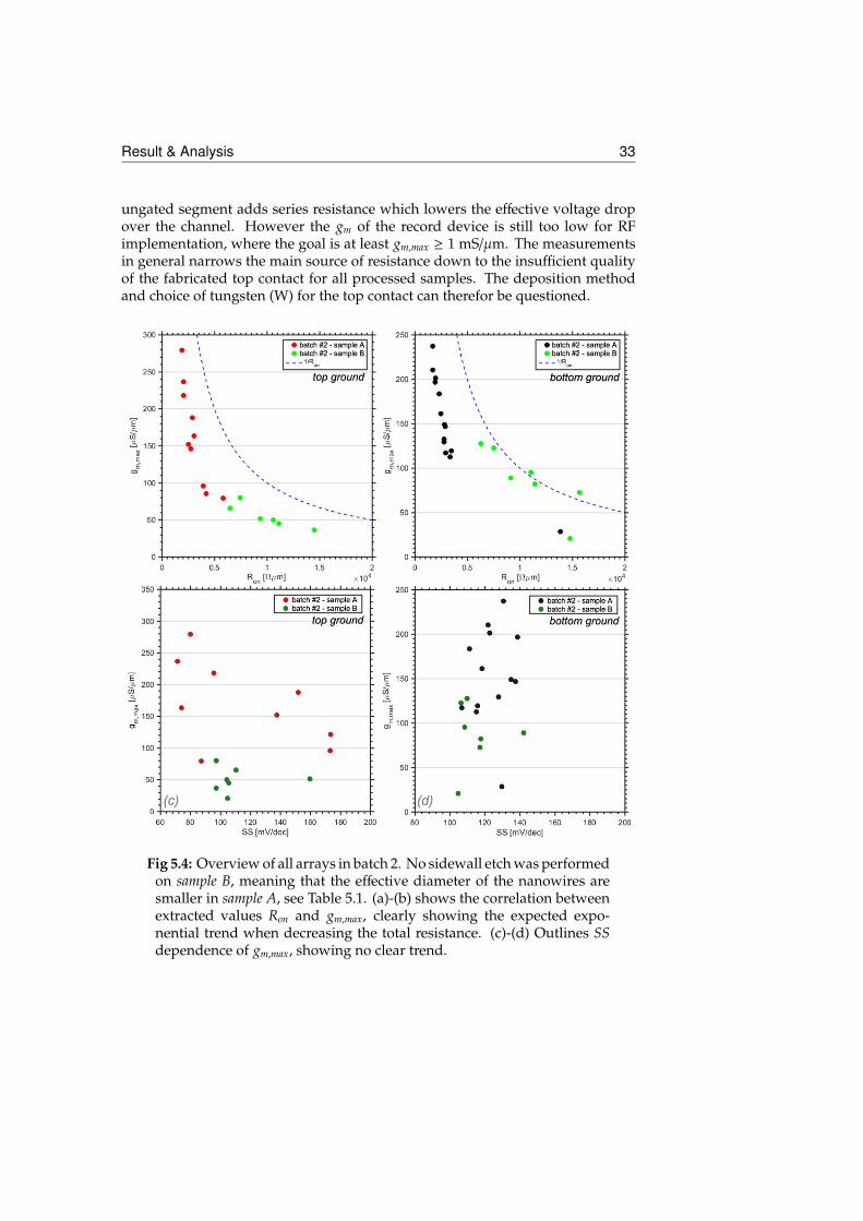
Result & Analysis 33
ungated segment adds series resistance which lowers the effective voltage dropover the channel. However the gm of the record device is still too low for RFimplementation, where the goal is at least gm,max ≥ 1 mS/µm. The measurementsin general narrows the main source of resistance down to the insufficient qualityof the fabricated top contact for all processed samples. The deposition methodand choice of tungsten (W) for the top contact can therefor be questioned.
Fig 5.4: Overview of all arrays in batch 2. No sidewall etch was performedon sample B, meaning that the effective diameter of the nanowires aresmaller in sample A, see Table 5.1. (a)-(b) shows the correlation betweenextracted values Ron and gm,max, clearly showing the expected expo-nential trend when decreasing the total resistance. (c)-(d) Outlines SSdependence of gm,max, showing no clear trend.
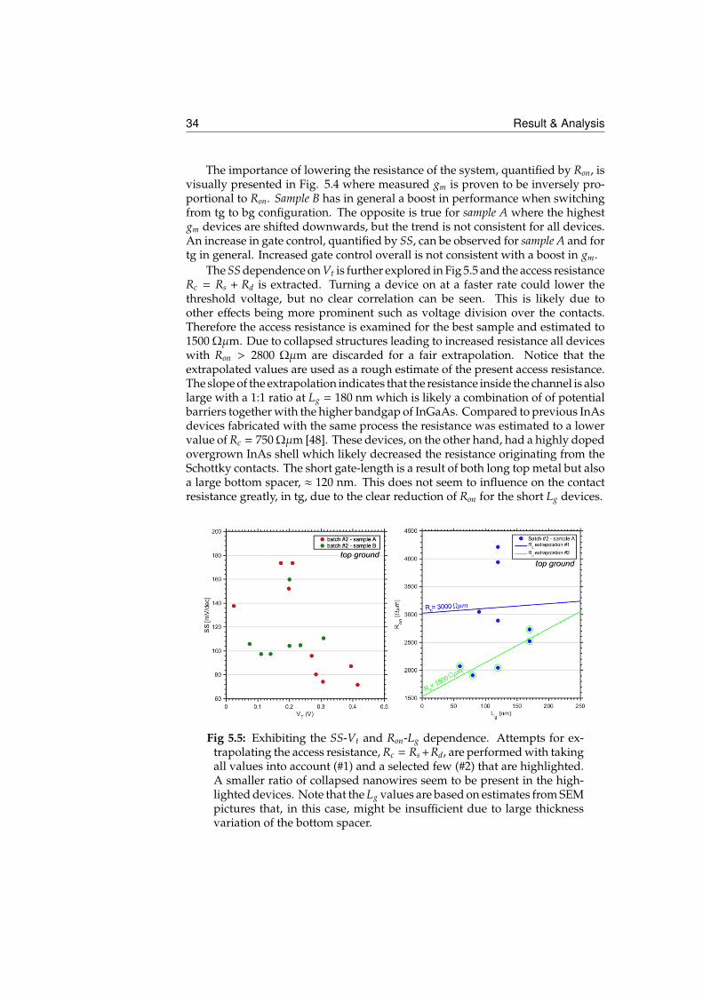
34 Result & Analysis
The importance of lowering the resistance of the system, quantified by Ron, isvisually presented in Fig. 5.4 where measured gm is proven to be inversely pro-portional to Ron. Sample B has in general a boost in performance when switchingfrom tg to bg configuration. The opposite is true for sample A where the highestgm devices are shifted downwards, but the trend is not consistent for all devices.An increase in gate control, quantified by SS, can be observed for sample A and fortg in general. Increased gate control overall is not consistent with a boost in gm.
The SS dependence on Vt is further explored in Fig 5.5 and the access resistanceRc = Rs + Rd is extracted. Turning a device on at a faster rate could lower thethreshold voltage, but no clear correlation can be seen. This is likely due toother effects being more prominent such as voltage division over the contacts.Therefore the access resistance is examined for the best sample and estimated to1500 Ωµm. Due to collapsed structures leading to increased resistance all deviceswith Ron > 2800 Ωµm are discarded for a fair extrapolation. Notice that theextrapolated values are used as a rough estimate of the present access resistance.The slope of the extrapolation indicates that the resistance inside the channel is alsolarge with a 1:1 ratio at Lg = 180 nm which is likely a combination of of potentialbarriers together with the higher bandgap of InGaAs. Compared to previous InAsdevices fabricated with the same process the resistance was estimated to a lowervalue of Rc = 750 Ωµm [48]. These devices, on the other hand, had a highly dopedovergrown InAs shell which likely decreased the resistance originating from theSchottky contacts. The short gate-length is a result of both long top metal but alsoa large bottom spacer, ≈ 120 nm. This does not seem to influence on the contactresistance greatly, in tg, due to the clear reduction of Ron for the short Lg devices.
Fig 5.5: Exhibiting the SS-Vt and Ron-Lg dependence. Attempts for ex-trapolating the access resistance, Rc = Rs +Rd, are performed with takingall values into account (#1) and a selected few (#2) that are highlighted.A smaller ratio of collapsed nanowires seem to be present in the high-lighted devices. Note that the Lg values are based on estimates from SEMpictures that, in this case, might be insufficient due to large thicknessvariation of the bottom spacer.
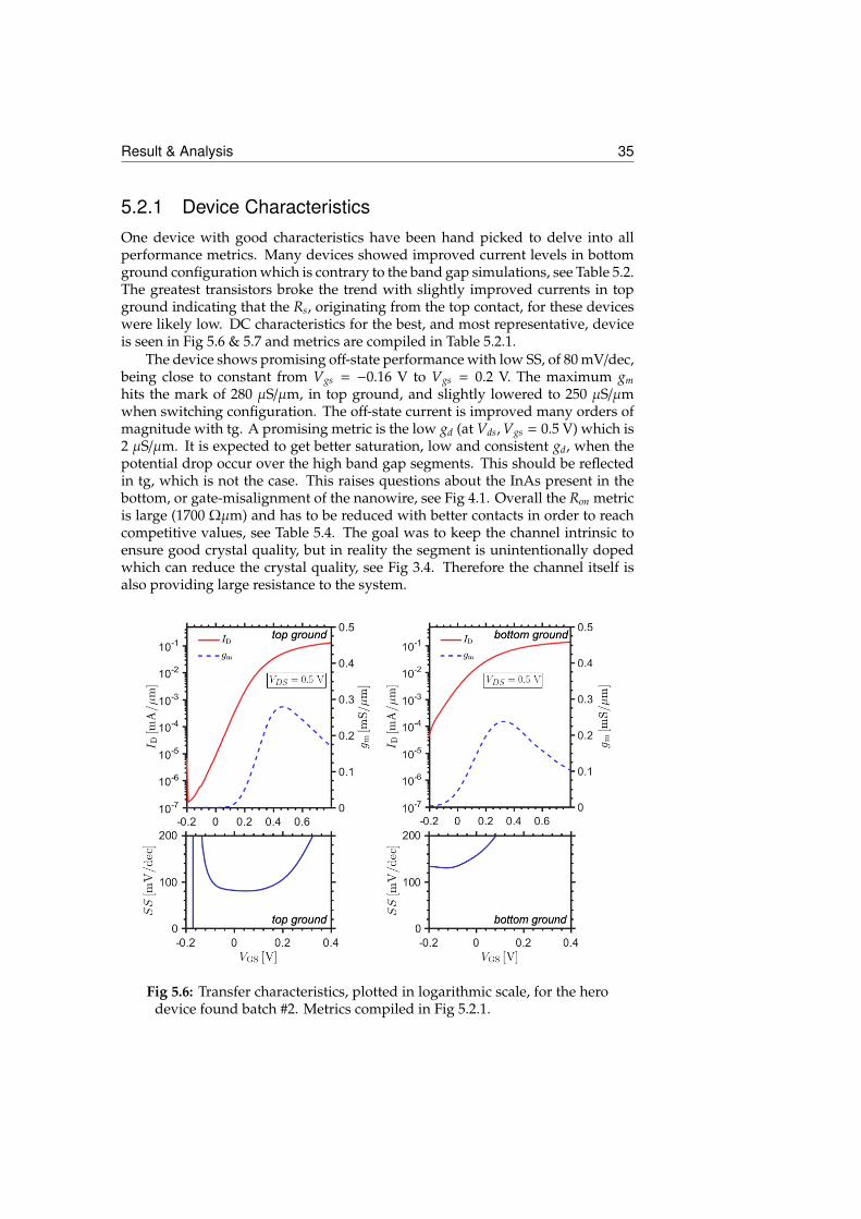
Result & Analysis 35
5.2.1 Device CharacteristicsOne device with good characteristics have been hand picked to delve into allperformance metrics. Many devices showed improved current levels in bottomground configuration which is contrary to the band gap simulations, see Table 5.2.The greatest transistors broke the trend with slightly improved currents in topground indicating that the Rs, originating from the top contact, for these deviceswere likely low. DC characteristics for the best, and most representative, deviceis seen in Fig 5.6 & 5.7 and metrics are compiled in Table 5.2.1.
The device shows promising off-state performance with low SS, of 80 mV/dec,being close to constant from Vgs = −0.16 V to Vgs = 0.2 V. The maximum gmhits the mark of 280 µS/µm, in top ground, and slightly lowered to 250 µS/µmwhen switching configuration. The off-state current is improved many orders ofmagnitude with tg. A promising metric is the low gd (at Vds,Vgs = 0.5 V) which is2 µS/µm. It is expected to get better saturation, low and consistent gd, when thepotential drop occur over the high band gap segments. This should be reflectedin tg, which is not the case. This raises questions about the InAs present in thebottom, or gate-misalignment of the nanowire, see Fig 4.1. Overall the Ron metricis large (1700 Ωµm) and has to be reduced with better contacts in order to reachcompetitive values, see Table 5.4. The goal was to keep the channel intrinsic toensure good crystal quality, but in reality the segment is unintentionally dopedwhich can reduce the crystal quality, see Fig 3.4. Therefore the channel itself isalso providing large resistance to the system.
Fig 5.6: Transfer characteristics, plotted in logarithmic scale, for the herodevice found batch #2. Metrics compiled in Fig 5.2.1.
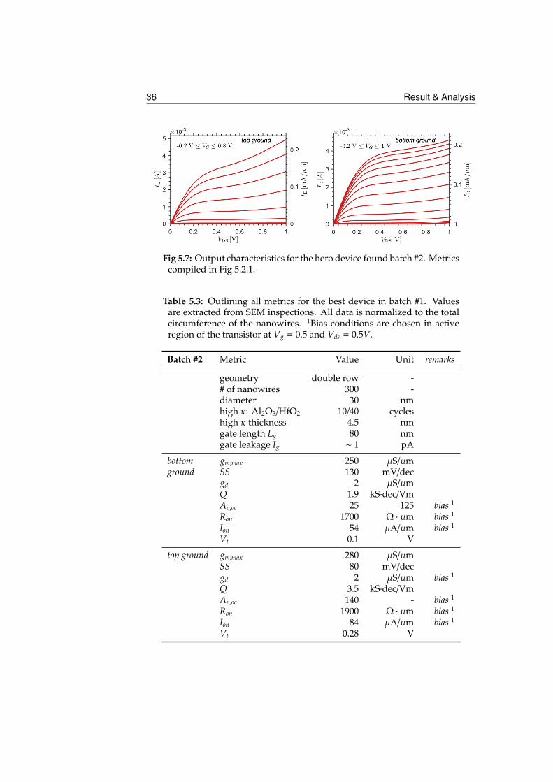
36 Result & Analysis
Fig 5.7: Output characteristics for the hero device found batch #2. Metricscompiled in Fig 5.2.1.
Table 5.3: Outlining all metrics for the best device in batch #1. Valuesare extracted from SEM inspections. All data is normalized to the totalcircumference of the nanowires. 1Bias conditions are chosen in activeregion of the transistor at Vg = 0.5 and Vds = 0.5V.
Batch #2 Metric Value Unit remarks
geometry double row -# of nanowires 300 -diameter 30 nmhigh κ: Al2O3/HfO2 10/40 cycleshigh κ thickness 4.5 nmgate length Lg 80 nmgate leakage Ig ∼ 1 pA
bottom gm,max 250 µS/µmground SS 130 mV/dec
gd 2 µS/µmQ 1.9 kS·dec/VmAv,oc 25 125 bias 1
Ron 1700 Ω · µm bias 1
Ion 54 µA/µm bias 1
Vt 0.1 V
top ground gm,max 280 µS/µmSS 80 mV/decgd 2 µS/µm bias 1
Q 3.5 kS·dec/VmAv,oc 140 - bias 1
Ron 1900 Ω · µm bias 1
Ion 84 µA/µm bias 1
Vt 0.28 V
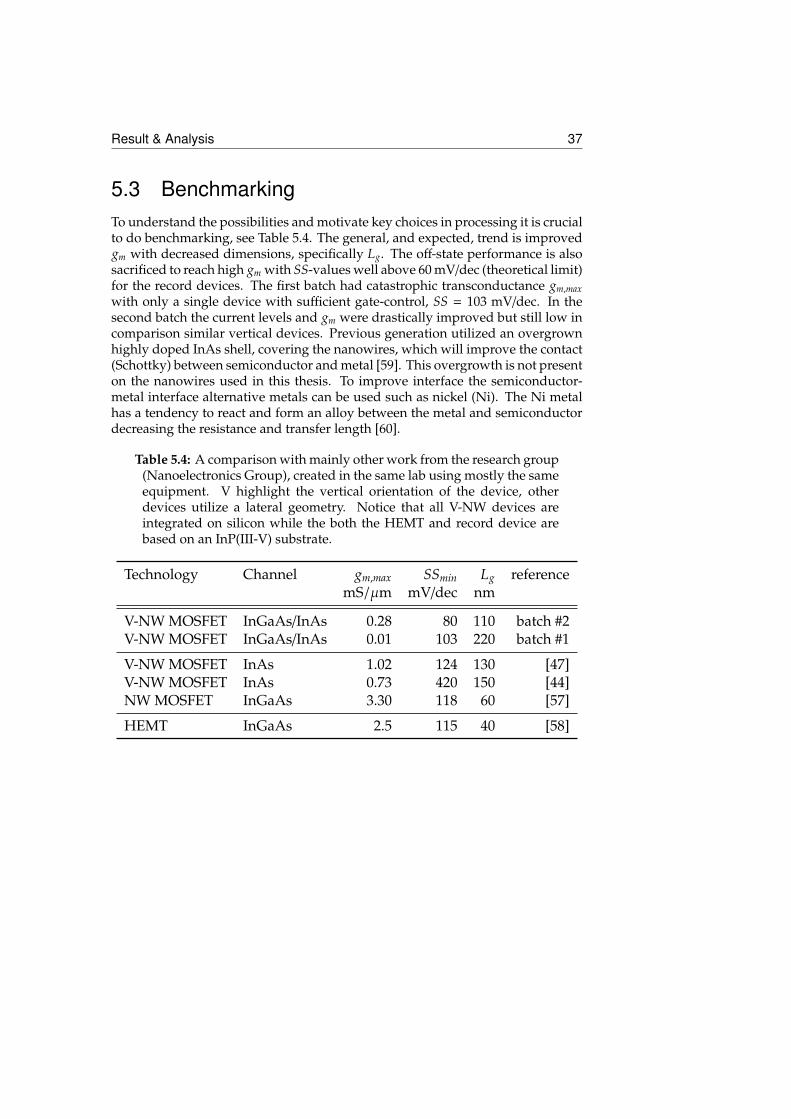
Result & Analysis 37
5.3 BenchmarkingTo understand the possibilities and motivate key choices in processing it is crucialto do benchmarking, see Table 5.4. The general, and expected, trend is improvedgm with decreased dimensions, specifically Lg. The off-state performance is alsosacrificed to reach high gm with SS-values well above 60 mV/dec (theoretical limit)for the record devices. The first batch had catastrophic transconductance gm,maxwith only a single device with sufficient gate-control, SS = 103 mV/dec. In thesecond batch the current levels and gm were drastically improved but still low incomparison similar vertical devices. Previous generation utilized an overgrownhighly doped InAs shell, covering the nanowires, which will improve the contact(Schottky) between semiconductor and metal [59]. This overgrowth is not presenton the nanowires used in this thesis. To improve interface the semiconductor-metal interface alternative metals can be used such as nickel (Ni). The Ni metalhas a tendency to react and form an alloy between the metal and semiconductordecreasing the resistance and transfer length [60].
Table 5.4: A comparison with mainly other work from the research group(Nanoelectronics Group), created in the same lab using mostly the sameequipment. V highlight the vertical orientation of the device, otherdevices utilize a lateral geometry. Notice that all V-NW devices areintegrated on silicon while the both the HEMT and record device arebased on an InP(III-V) substrate.
Technology Channel gm,max SSmin Lg referencemS/µm mV/dec nm
V-NW MOSFET InGaAs/InAs 0.28 80 110 batch #2V-NW MOSFET InGaAs/InAs 0.01 103 220 batch #1
V-NW MOSFET InAs 1.02 124 130 [47]V-NW MOSFET InAs 0.73 420 150 [44]NW MOSFET InGaAs 3.30 118 60 [57]
HEMT InGaAs 2.5 115 40 [58]
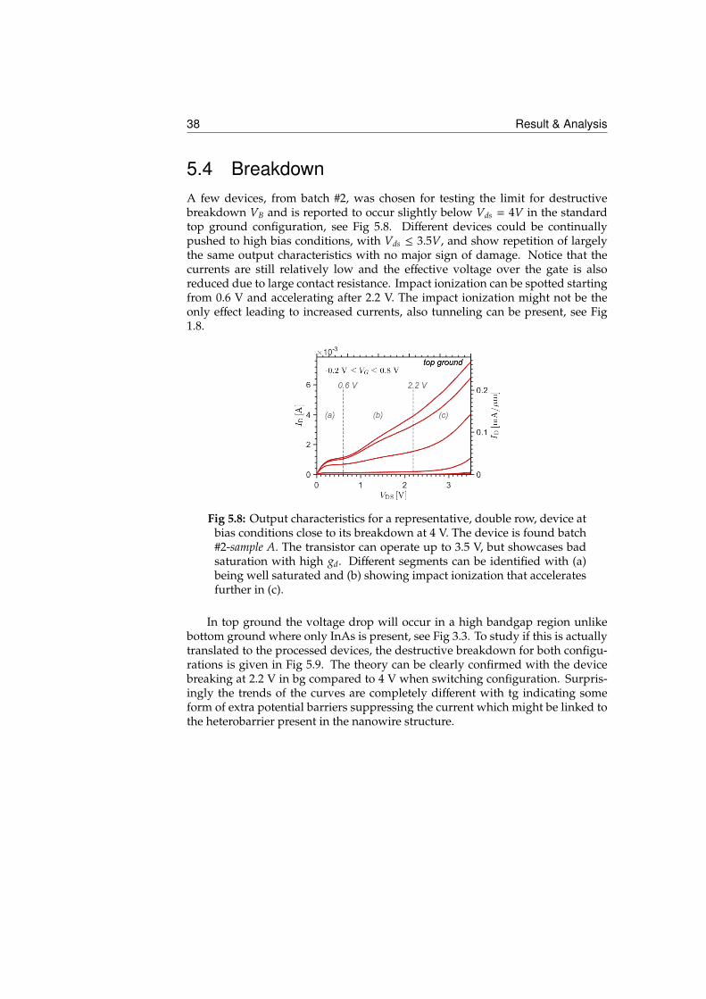
38 Result & Analysis
5.4 BreakdownA few devices, from batch #2, was chosen for testing the limit for destructivebreakdown VB and is reported to occur slightly below Vds = 4V in the standardtop ground configuration, see Fig 5.8. Different devices could be continuallypushed to high bias conditions, with Vds ≤ 3.5V, and show repetition of largelythe same output characteristics with no major sign of damage. Notice that thecurrents are still relatively low and the effective voltage over the gate is alsoreduced due to large contact resistance. Impact ionization can be spotted startingfrom 0.6 V and accelerating after 2.2 V. The impact ionization might not be theonly effect leading to increased currents, also tunneling can be present, see Fig1.8.
Fig 5.8: Output characteristics for a representative, double row, device atbias conditions close to its breakdown at 4 V. The device is found batch#2-sample A. The transistor can operate up to 3.5 V, but showcases badsaturation with high gd. Different segments can be identified with (a)being well saturated and (b) showing impact ionization that acceleratesfurther in (c).
In top ground the voltage drop will occur in a high bandgap region unlikebottom ground where only InAs is present, see Fig 3.3. To study if this is actuallytranslated to the processed devices, the destructive breakdown for both configu-rations is given in Fig 5.9. The theory can be clearly confirmed with the devicebreaking at 2.2 V in bg compared to 4 V when switching configuration. Surpris-ingly the trends of the curves are completely different with tg indicating someform of extra potential barriers suppressing the current which might be linked tothe heterobarrier present in the nanowire structure.
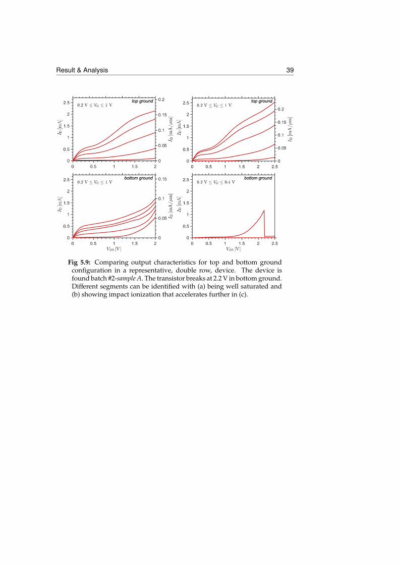
Result & Analysis 39
Fig 5.9: Comparing output characteristics for top and bottom groundconfiguration in a representative, double row, device. The device isfound batch #2-sample A. The transistor breaks at 2.2 V in bottom ground.Different segments can be identified with (a) being well saturated and(b) showing impact ionization that accelerates further in (c).

40 Result & Analysis
Chapter6Conclusion & Outlook
The benefits of introducing an InGaAs/InAs heterostructure as channel materialhas proven necessary for improved stability of the transistors, with good satura-tion of gd. In the end mixing of III-V materials is a great advantage and possibil-ity when utilizing the bottom up approach with epitaxial growth of nanowires.Therefore this study has served to gain evidence of the quality and control ofgrowth techniques. Initially the control of doping was questioned, if the in-situdoping would provide enough precision for doping of the short bottom segmentpresent at the drain side while keeping the channel close to intrinsic (uninten-tionally doped). The typical characteristics of a junctionless transistor is badmodulation of current and a depletion type transistor (on-state by default). Theprocessed transistors exhibit none of these behaviours with Vt > 0 V and SS < 90mV/dec.
Quality of the bi-layer high-κ is also surprisingly good (low SS and gateleakage) and is likely connected to the state of the ALD chamber. Nonethelessit proves the presence of a good nanowire surface for the high-κ interface andmotivates further implementation of the bi-layer.
The created transistors are also commercially viable due to the III-V integrationon top of silicon. The geometry itself has conceptually many benefits with its GAAconfiguration and decoupling of footprint area with the actual length of the device.
The DC characteristics are insufficient for further investigation of RF capa-bilities due to the high resistance of the structure Rc ≈ 1500Ωµm and collapseof nanowires. Both of these problems can be addressed in the near future byutilizing shorter nanowires (∼ 300 nm), introducing annealing, better control ofthe ICP-RIE process and possibly using a highly doped overgrowth. The lattersteps are necessary for improvement of the metal-semiconductor junction, noticethat a change in top metal all together is also possible.
The orientation of the heterostructure lends itself to top grounded config-uration with the drain pad situated at the bottom. Which might prove usefuldue to heat developing in the substrate rather than top contact. After creatingmatching networks and other necessary circuity, in addition to the devices, heatdevelopment in the substrate is convenient for efficient cooling.
41

42 Conclusion & Outlook
References
[1] R. G. Arns, "The other transistor: Early history of the metal-oxide semicon-ductor field-effect transistor," Engineering Science and Education Journal, vol.7, issue 5, pp. 233–240 (1998)
[2] A. G. Levine, "John Bardeen, William Shockley, Walter Brattain; Invention ofthe transistor - Bell laboratories," APS physics (2010)
[3] G. E Moore, "Cramming more components onto integrated curcuits," Elec-tronics vol. 38, no. 8, pp. 114-117 (1965)
[4] D. J. Frank, "Power constrained CMOS scaling," IBM Journal of Research andDevelopment vol. 46, issue 2.3, pp. 235-244 (2010)
[5] F. Mattern & C. Floerkemeier, "From the internet of computers to the internetof things," Active Data Management on Event-Based Systems and More vol. 6462,pp. 242-259 (2010)
[6] A. Wacker, "Notes for solid state theory," Matematisk Fysik, Lund University,chapter 1, pp. 1–14 (2014)
[7] G. Grossman, "Fasta tillståndets fysik," Lund University, chapter 5, pp.113–143 (2014)
[8] C. R. Nave "The doping of semicondictors," Hyperphysics (2005)http://hyperphysics.phy-astr.gsu.edu/hbase/solids/dope.html
[9] NPTEL "Fundamental concepts of semiconductors," IIT DELHI (2013)http://nptel.ac.in/courses/115102025/8(2016-08-15)
[10] W. Mönch, "Role of Virtual Gap States and Defects in Metal-SemiconductorContacts," Universität Duisburg, vol. 4, pp 224-227, (1990)
[11] R. Islam et al., "Schottky barrier height reduction for holes by Fermi leveldepinning using metal/nickeloxide/silicon contacts," App. Phys. Let., No. 105,182103 (2014)
[12] S. E. Thompson et al., "Moore’s law: the future of Si microelectronics," Elsevierltd. vol. 9 (2006)
43
44 References
[13] Electronics Tutorial, "The MOSFET" (2014)http://www.electronics-tutorials.ws/transistor/tran_6.html/(2016-05-22)
[14] W. J. Dally & J. W. Poulton, "Digital System Engineering," Cambridge Univer-sity press p. 158 (1998)
[15] B. J. Zeghbroeck, "The energy band diagram of the Metal-Oxide-Silicon(MOS) Capacitor," chapter 6.2 (1996)http://ecee.colorado.edu/~bart/book/moseb.htm/
[16] W. Liu, "Fundamentals of III-V devices: HBTs, MESFETs, andHFETs/HEMTs," Wiley-Interscience publication (1999)
[17] H. Brech, "Optimization of GaAs based High Electron Mobility Transistorsby Numerical Simulations: The Principles of a HEMT," dissertation, chapter2 (1998)
[18] P. Abrahams et al., "Intel 22 nm 3-D tri-gate transistor technology," Intel (2011)newsroom.intel.com/press-kits/intel-22nm-3-d-tri-gate-transistor-technology/ (2016-07-15)
[19] L. M. Terman. "Solid State electronics: An investigation of surface states at asilicon/silicon oxide interface employing metal-oxide-silicon diodes," Elsevierltd., vol. 5, issue 5, pp. 285–299 (1962)
[20] J. Robertson et al. "Defect State Passivation at III-V – oxide Interfaces forCMOS devices ," J. Appl. Phys. no. 117, 112806 (2015)
[21] J. Wu et al., "Low Trap Density in InAs/High-k Nanowire Gate Stacks withOptimized Growth and Doping Conditions," Nanoletters (2016)
[22] R. S. Chau et al., "Intel’s Breakthrough in High-K Gate Dielectric DrivesMoore’s Law Well into the Future," Technology@Intel Magazine January (2004)
[23] G. Ribes et al., "Review on High-k Dielectrics Reliability Issues," IEEE vol. 5,No. 1 (2005)
[24] J. Robertson et al., "High dielectric constant oxides," Eur. Phys. J. Appl. Physvol. 28, pp. 365–291 (2004)
[25] D. Liang & J.E. Bowers, "Photonic integration: Si or InP substrates?" Elec-tronics Letter vol. 45, no. 12 (2009)
[26] L. C. Chuang et al., "Critical diameter for III-V nanowires grown on lattice-mismatched substrates," Appl. Phys. Lett. No. 90, 043115 (2007)
[27] D. Yakimets et al., "Vertical GAAFETs for the Ultimate CMOS scaling," IEEEpp. 1433-149, 15072197 (2015)
[28] J. A. del Alamo et al., "Nanometre-scale electronics with III–V compoundsemiconductors," Nature vol. 479, pp. 317–323 (2011)
[29] F. D’Agostino & D. Quercia, "Short channel effects in MOSFETs," VLSI report(2000)http://www0.cs.ucl.ac.uk/staff/ucacdxq/projects/vlsi/report.pdf/(2016-07-20)
References 45
[30] A Lubow et al., "Comparison of drive currents in metal-oxide-semiconductorfield-effect transistors made of Si, Ge, GaAs, InGaAs, and InAs channels,"App. Phys. Letter No 96 (2010)
[31] T. Pesic-Berdanin et al., "Strained Silicon Layer in CMOS Technology," Elec-tronics vol. 18, no. 2 (2014)
[32] J. Y. Tsao, "The world of compound semiconductors: A guidebook to the corescience and tehcnology," Sandia National Laboratories pp. 1-7 (2004)
[33] R. Kim et al., "Comprehensive performance benchmarking of III-V and Sinmosfets (gate length=13 nm) considering supply voltage and off-current,"Electron Devices, IEEE transactions on, vol. 62, no. 3, pp. 713-721 (2015)
[34] D. Kim et al., "Extraction of virtualsource injection velocity in sub-100 nmIII-V hfets," Electron Devices Meeting (IEDM), 2009 IEEE International, pp. 1-4(2009)
[35] R. Flückiger et al., "Type II InP/GaAsSb double-heterojunction bipolar tran-sistor with fMAX > 700 GHz," Applied Physics Exress vol. 7 (2004)
[36] E. O. Kane et al., "Theory of tunneling," Journal of applied physics (1961)
[37] J. H. Davies et al., "The physics of low-dimensional semiconductors," Cam-bridge University Press, Appendix 2, pp. 410-411 (2009)
[38] X. Mei et al., "First demonstration of Amplification at 1 THz Using 25-nmInP High Electron Mobility Transistor," IEEE Electronic Device Letters vol. 36(2015)
[39] W. Maes et al., "IMPACT IONIZATION IN SILICON: A REVIEW AND UP-DATE ," Solid-State electronics, vol. 33, No. 6, pp 705-718 (1990)
[40] O. Triebl et al., "Reliability issues in High Voltage Semiconductors," ViennaUniversity chapter 5.1, (2013)
[41] W. Jo et al., "First Demonstration of GaN based Vertical Wanowire FET withTop-Down approach," IEEE (2015)
[42] T. Krishnamohan et al., "Double-Gate Strained-Ge Heterostructure TunnelingFET (TFET) With Record High Drive Currents and <60mV/dec SubthresholdSlope," IEEE, Stanford University, CA (2008)
[43] G. Constable et al., "A century of innovation: Twenty engineeringachievements that transformed our lives," Joseph Henry Press (2003)http://www.greatachievements.org/?id=3956(2016-07-16)
[44] S. Johansson et al., "RF Characterization of Vertical InAs Nanowire MOSFETswith ft and fmax above 140 GHz," IEEE, Lund University (2010)
[45] B. Feng et al., "Schottky barrier heights at the interfaces between pure-phaseInAs nanowires and metal contacts," J. Appl. Phys. 119, 054304 (2016)
[46] Sofia. Johansson, "Vertical Nanowire High-Frequency transistors," EIT, LundUniversity Doctoral dissertation (2014)
46 References
[47] M. Berg, "Vertical InAs Nanowire Devices and RF circuits," EIT, Lund Uni-versity Doctoral thesis (2015)
[48] M. Berg et al., "Self-Aligned, Gate-Last Process for Vertical InAs NanowireMOSFETs on Si," IEDM15-805, Lund University (2015)
[49] J. Wu et al. "Control of composition and morphology in InGaAs nanowiresgrown by metalorganic vapor phase epitaxy," Journal of crystal growth vol.383, pp 158-165 (2016)
[50] J. Wu, "Vertical III-V/High-k Nanowire MOS Capacitors and Transistors,"EIT, Lund University, doctoral thesis (2016)
[51] H. J. Choi et al., "Semiconductor Nanostructures for optoelectronic devices,"Springer-Verlag chapter 1, pp. 3-10 (2012)
[52] W. Ahmed et al., "Ion implantation and in-situ doping of silicon," Materials,Chemistry & Physics, 37, pp. 289-294 (1994)
[53] Dow Corning corporation., "Information about FOx-1x and FOx-2x flowableoxides," Product Information, No. 10-713A-01 (2005)
[54] E. Memisevic et al., "The electron beam defined hydrogen sisesquioxanespacers for vertical nanowire transistors," JVSTB, 32, 051211 (2005)
[55] ROHMHAAS Electronic Materials., "Material Safety Data Sheet; MF319"(2004)
[56] J. J. Hill et al., "Eliminating Capillary Coalescence of Nanowire Arrays withApplied Electric Fields", ACS Appl. Mater. Interfaces, 2 (7), pp 1992–1998 (2010)
[57] C. B. Zota et al., "Single suspended InGaAs nanowire MOSFETs", IEDM15-811, (2015)
[58] X. Zhao et al., "Vertical nanowire ingaas mosfets fabricated by a top-downapproach," IEDM, (2013)
[59] J. M. Shannon et al. "Control of Schottky barrier height using highly dopedsurface layers," Elsevier ltd., vol. 19, issue 6, pp 537-543 (1976)
[60] S. H. Kim et al. "Self-Aligned Metal Source/Drain InxGa1-xAs n-Metal–Oxide–Semiconductor Field-Effect Transistors Using Ni–InGaAs Al-loy," Applied Physics Express, vol. 4, no. 2 (2011)
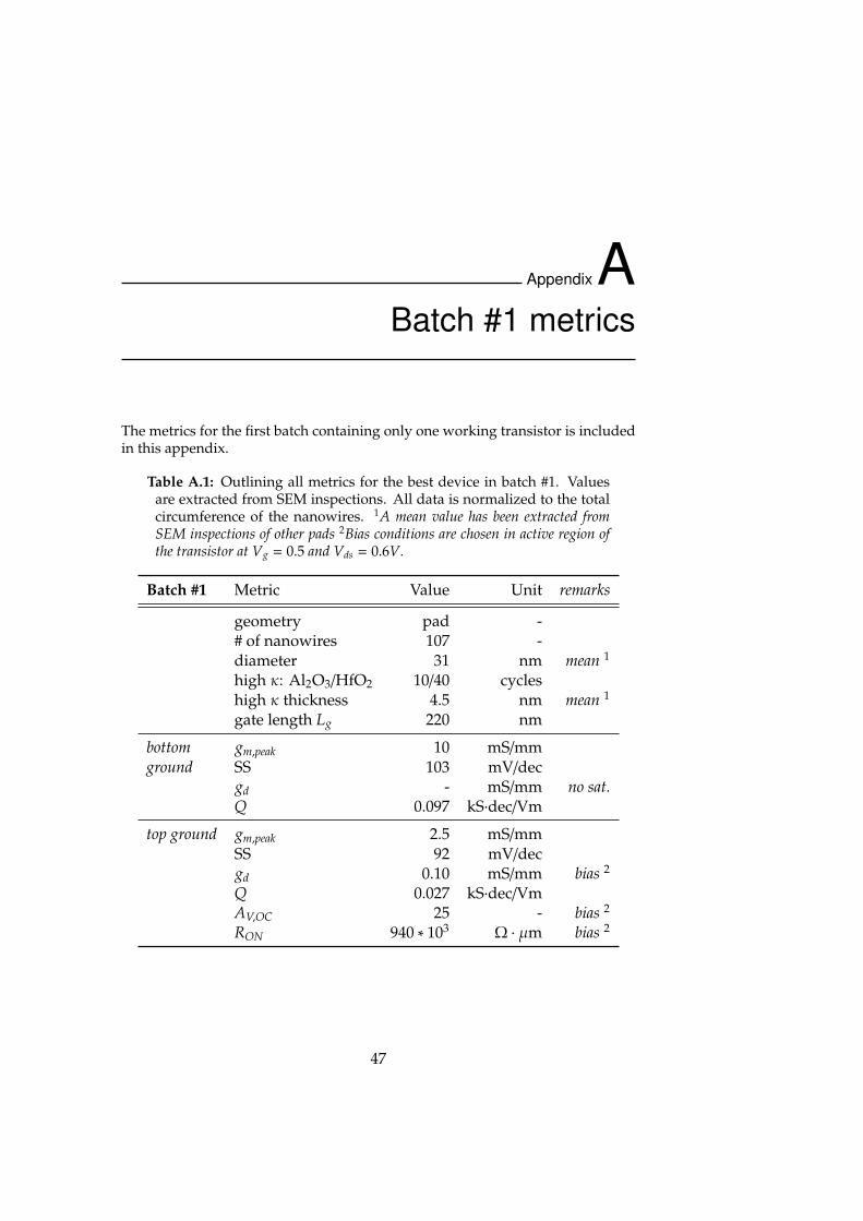
AppendixABatch #1 metrics
The metrics for the first batch containing only one working transistor is includedin this appendix.
Table A.1: Outlining all metrics for the best device in batch #1. Valuesare extracted from SEM inspections. All data is normalized to the totalcircumference of the nanowires. 1A mean value has been extracted fromSEM inspections of other pads 2Bias conditions are chosen in active region ofthe transistor at Vg = 0.5 and Vds = 0.6V.
Batch #1 Metric Value Unit remarks
geometry pad -# of nanowires 107 -diameter 31 nm mean 1
high κ: Al2O3/HfO2 10/40 cycleshigh κ thickness 4.5 nm mean 1
gate length Lg 220 nm
bottom gm,peak 10 mS/mmground SS 103 mV/dec
gd - mS/mm no sat.Q 0.097 kS·dec/Vm
top ground gm,peak 2.5 mS/mmSS 92 mV/decgd 0.10 mS/mm bias 2
Q 0.027 kS·dec/VmAV,OC 25 - bias 2
RON 940 ∗ 103 Ω · µm bias 2
47

Vertical H
eterostru
cture III-V
Nan
ow
ire MO
SFETs
Department of Electrical and Information Technology, Faculty of Engineering, LTH, Lund University, 2016.
Vertical Heterostructure III-VNanowire MOSFETs
Adam Jönsson
Series of Master’s thesesDepartment of Electrical and Information Technology
LU/LTH-EIT 2016-537http://www.eit.lth.se
Ad
am
Jön
sson
Master’s Thesis


