Embed Size (px)
Citation preview

© 2014 IEEE. Personal use of this material is permitted. Permission from IEEE must be obtained for
all other uses, in any current or future media, including reprinting/republishing this material for
advertising or promotional purposes, creating new collective works, for resale or redistribution to
servers or lists, or reuse of any copyrighted component of this work in other works.
Digital Object Identifier (DOI): 10.1109/TPEL.2013.2262057
IEEE Transactions on Power Electronics, vol. 29, no. 3, pp. 1163-1175, March 2014.
Use of a Series Voltage Compensator for Reduction of the DC-Link Capacitance in a
Capacitor-Supported System
Huai Wang
Henry Shu-Hung Chung
Wenchao Liu
Suggested Citation
H. Wang, H. S. H. Chung, and W. Liu, "A new concept of high-voltage DC–DC conversion using
asymmetric voltage distribution on the switch pairs and hybrid ZVS–ZCS scheme," IEEE Trans. on
Power Electron., vol. 29, no. 3, pp. 1163-1175, Mar. 2014.

IEEE TRANSACTIONS ON POWER ELECTRONICS, VOL. 29, NO. 3, MARCH 2014 1163
Use of a Series Voltage Compensator for Reduction
of the DC-Link Capacitance in a
Capacitor-Supported SystemHuai Wang, Member, IEEE, Henry Shu-Hung Chung, Senior Member, IEEE, and Wenchao Liu
Abstract—A technique for reduction of the dc-link capacitancein a capacitor-supported system is presented. The concept is basedon connecting a voltage source in series with the dc bus line to com-pensate the ripple voltage on the dc-link capacitor, so as to makethe output have a near zero ripple voltage. Since the voltage com-pensator processes small ripple voltage on the dc link and reactivepower only, it can be implemented with low-voltage devices. Theoverall required energy storage of the dc-link, formed by a reducedvalue of dc-link capacitor and the voltage compensator, is reduced,allowing the replacement of popularly used electrolytic capacitorswith alternatives of longer lifetime, like power film capacitors, orextending the system lifetime even if there is a significant reductionin the capacitance of electrolytic capacitors due to the aging effect.Comprehensive analysis on the static and dynamic characteristicsof the system, and hold-up time requirement will be discussed.The proposed technique is exemplified on an ac–dc–dc power con-version system. Theoretical predictions are favorably verified byexperimental results.
Index Terms—Capacitance reduction, dc-link capacitor, powerconversion system, voltage compensator.
NOMENCLATURE
C DC-link capacitor.
CDC Input capacitor of the voltage compensator.
Lf Output filter inductance of the voltage compensator.
Cf Output filter capacitance of the voltage compensator.
vab Output voltage of the voltage compensator.
Vab Amplitude of vab .
Vab,rms Root-mean-square value of vab .
vC DC-link voltage.
Manuscript received September 22, 2012; revised January 5, 2013 and March6, 2013; accepted May 1, 2013. Date of current version September 18, 2013. Thiswork was supported in part by a grant from the Research Grants Council of theHong Kong Special Administrative Region, China, under Project CityU 112512.This paper was presented in part at the IEEE Energy Conversion Congress andExposition 2011, Phoenix, AZ, USA, the IEEE Applied Power ElectronicsConference and Exposition 2012, Orlando, FL, USA, and the IEEE EnergyConversion Congress and Exposition 2012, Raleigh, NC, USA. Recommendedfor publication by Associate Editor T. Shimizu.
H. Wang is with the Department of Energy Technology, Center of ReliablePower Electronics (CORPE), Aalborg University, DK-9220 Aalborg, Denmark(e-mail: [email protected]).
H. S.-H. Chung and W. Liu are with the Centre for Smart Energy Conversionand Utilization Research, City University of Hong Kong, Kowloon, Hong Kong(e-mail: [email protected]; [email protected]).
Color versions of one or more of the figures in this paper are available onlineat http://ieeexplore.ieee.org.
Digital Object Identifier 10.1109/TPEL.2013.2262057
VC DC component of vC .
vC (0) Voltage of vC in the event of an input power outage
of the front-end converter [vC (0) = VC − |∆vC |].∆vC AC component of vC .
∆VC,rms Root-mean-square value of ∆vC .
|∆vC | Amplitude of ∆vC .
vcon Control signal in the control stage of the voltage
compensator.
Vcon Amplitude of vcon .
vd Output voltage of the dc-link module.
Vd,min Specified minimum dc-link voltage during the hold-
up time period.
VD DC component of vd .
|∆vd | Amplitude of the voltage ripple component of vd .
vDC Input voltage of the voltage compensator.
VDC ,ref Input voltage reference of the voltage compensator.
vDC ,min Minimum value of vDC .
vDC(0) Voltage of vDC in the event of an input power outage
of the front-end converter [vDC(0) = vDC ,ref ].
|∆vDC | Amplitude of the voltage ripple component of vDC .
vos Offset voltage in the control stage of the voltage
compensator.
Vos DC component of vos .
|∆vos | Amplitude of the voltage ripple component of vos .
vout Output voltage of the phase-shifted full-bridge dc-dc
converter.
vtri Carrier signal of the PWM of the voltage compen-
sator.
Vtri Amplitude of vtri .
ia Current flowing through the input side of the dc-link
capacitor/module bus line.
IA Dc component of ia .
∆ia Ac component of ia .
|∆Ia | Amplitude of ∆ia .
iC Current following through the dc-link capacitor C.
|∆IC | Amplitude of iC .
iC f Current flowing through Cf .
id Current flowing through the output side of the dc-link
capacitor/module bus line.
Id,rms Root-mean-square value of id .
ID DC component of id .
∆id AC component of id .
|∆Id | Amplitude of ∆id .
iout Output current of the phase-shifted full-bridge dc–dc
converter.
frip Frequency of ∆vC .
0885-8993 © 2013 IEEE

1164 IEEE TRANSACTIONS ON POWER ELECTRONICS, VOL. 29, NO. 3, MARCH 2014
M Modulation index of ratio Vcon / Vtri .
Pab Average power absorbed by the voltage compensator.
Sab Apparent power handled by the voltage compensator.
Sm Apparent power handled by the main circuit.
T Least common multiple of 2π/ω1 and 2π/ω2 .
α Scaling factor of vC in the control stage to the PWM
controller.
β Ratio between |∆IC | and ID .
γ Ratio between vDC(0) and |∆vC |.δ1 Phase of ∆ia .
δ2 Phase of ∆id .
λ Ratio between C and CDC .
µ Ratio between |∆vC | and VC .
ρ Ratio between Vd,min and VC .
ω Angular frequency of the capacitor ripple current
(ω = 2πfrip).ω1 Frequency of ∆ia .
ω2 Frequency of ∆id .
N Number of hold-up cycles with respect to the period
of the dc-link voltage ripple with the proposed dc-
link module.
I. INTRODUCTION
ACAPACITOR-supported system consists of multiple
power converters interconnected by a dc link. The dc-link
voltage is maintained by a capacitor bank that absorbs instan-
taneous power difference between the input source and output
load, minimizing voltage variation on the dc link, and providing
sufficient energy during the hold-up time of the system. Among
different types of capacitor, aluminum electrolytic capacitors
(E-Caps) are the most popular choice because of their high vol-
umetric efficiency and low cost. However, they suffer from the
drawbacks of high equivalent series resistance (ESR); low rip-
ple current capability; bottleneck of the voltage rating; relatively
short lifetime compared to other components; and considerable
maintenance work.
Advances in power film capacitor technology are emerging
for dc-link filtering [1], [2]. Power film capacitors outperform
aluminum E-Caps in terms of ESR, self-healing capability, life
expectancy, environmental performance, dc-blocking capability,
ripple current capability, and reliability. Although low-voltage
and high-value film capacitors are available, the capacitance
of the high-voltage film capacitors still cannot compete with
E-Caps, due to their relatively low volumetric efficiency and
high cost. To lessen the dependency of the dc-link capacitance,
there are many prior-art methods, based on the following ap-
proaches:
1) Performance trade-off:- This method allows a larger volt-
age ripple across the dc link with a smaller capacitance.
However, it is practically less impressive as the system
performance will be degraded. It is more suitable for cer-
tain applications, like the ones in [3]–[5]. A set of design
procedure is given in [6] for the optimization of capacitor
bank.
2) Reduction of the dc-link capacitor current with sophisti-
cated control: The concept is based on reducing the ripple
current flowing through the dc-link capacitor [7]–[12]. The
front-stage converter is an active rectifier in [7]–[10], and
a step-up dc–dc converter in [11], [12], while the output is
an inverter. Their key advantage is that no additional cir-
cuit is needed. However, those control methods cannot be
applied to systems with front-end diode-bridge rectifier.
Apart from requiring a sophisticated controller, some of
them also rely on specific relationship in the operating fre-
quency between the converters connected [7], [10], [11].
The method given in [8] is limited to three-phase systems.
The controller described in [7] is based on assuming an
ideal energy conversion. Thus, the actual input current
would be distorted unless multiple cell load inverters are
used. The performance of those controllers is greatly de-
pendent on the accuracy of the computations [9], [12]
and affected by the overall time delays of the control
loops.
3) Increase in the frequency of the dc-link voltage ripple:
A double frequency front-end converter with multiphase
switching is proposed in [13] to reduce the ripple voltage.
However, the approach cannot reduce the dc-link capaci-
tance significantly.
4) Ripple cancellation circuit with a coupled element: In
[14], a coupled inductor is applied to cancel the voltage
ripple of the dc input, dc output, or dc link of a power con-
verter. The concept is based on assuming that the capacitor
used in the storage tank is infinite. But in reality, the capac-
itance has a finite value, and the coupled inductor filter and
the capacitor form a low-pass filter. To avoid large-sized
coupled windings, the technique is more suitable for fil-
tering high-frequency ripples or noise, such as switching
ripple, EMI filtering. Moreover, the dynamic response of
the capacitor may be degraded due to the series-connected
coupled winding.
Apart from the aforementioned methods, active power filters
can also be used for reduction of the dc-link capacitance as pre-
sented in [15]–[28]. It is based on connecting an auxiliary circuit
in parallel with the dc-link capacitor. The added circuit serves as
an active impedance or energy source. Different methods of im-
plementing the auxiliary circuit are given. In [16], the auxiliary
circuit has a single switch with a dissipative resistor. In [20], a
relay is placed at the input line and is activated, depending on the
dc-link voltage level, resulting in a stable dc-link voltage, but
at the expense of reducing the input power factor of the entire
system. In [15], [17], and [22], an H-bridge circuit with a cur-
rent source (inductor) is used to minimize the ripple current of
the dc-link capacitor. However, the high inductor current stress
and high switching frequency requirement in [22] are the major
practical challenges of the method. A current injection method
was applied in [18], [19], [21], and [23] by a half-bridge struc-
ture. In [24] and [25], a two-switch converter that can operate
bidirectionally in both buck and boost modes is used for the
H-bridge front-end and dc current electrical load application.
In [26], a series-connected dual boost converter is as the shunt
active filter for a three-phase diode rectifier front-end conversion
system. In [27], the ripple reduction circuit allows an additional
power port for enhancing the dynamic response of the whole

WANG et al.: USE OF A SERIES VOLTAGE COMPENSATOR FOR REDUCTION OF THE DC-LINK CAPACITANCE 1165
Fig. 1. Basic concept of the proposed dc-link module.
system. In [28], a single switch, diode, and capacitor circuit is
added in parallel with the input capacitor of a microinverter to
reduce the overall capacitance requirement. The common chal-
lenge of all these methods is that the components used in the
auxiliary circuit are under a high voltage stress, which could
be as high as the dc-link voltage. Moreover, the impact of the
active filters on the hold-up behavior of the dc-link has not been
explored in [15]–[28].
This paper presents a module that can reduce the required dc-
link capacitance. Its operating principle is based on connecting a
series voltage source between the dc-link capacitor and the load.
The energy storage in the whole system is reduced, making
it possible to replace the high-value E-Caps with low-value
high-performance capacitors. The voltage compensator is of low
voltage and low power rating, as it only produces low voltage
and handles reactive power.
II. PROPOSED MODULE FOR DC-LINK
CAPACITANCE REDUCTION
Fig. 1 illustrates the basic concept of the module for reducing
the dc-link capacitance. The module is composed of a capacitor
C and a voltage source vab . The module is connected between
two converters, namely Converter 1 and Converter 2. The ca-
pacitor voltage vC has dc component VC and ripple voltage
∆vC . The peak-to-peak value and ripple frequency of ∆vC are
2|∆vC | and frip , respectively. vab is connected in series between
the capacitor CvC and the input of Converter 2 vd . It generates a

1166 IEEE TRANSACTIONS ON POWER ELECTRONICS, VOL. 29, NO. 3, MARCH 2014
Fig. 2. Control mechanism with a capacitor as the input source of the voltagecompensator.
voltage counteracting ∆vC with its dc component equal to zero
(i.e., vab = ∆vC ). Thus, vd has the same dc value as that across
C, but with a zero ripple voltage under the ideal condition. Such
architecture allows a high voltage ripple on C, implying that the
value of C can be made smaller, but at the expense of increasing
the magnitude of vab .
vab is a dc–ac converter with a full-bridge (FB) circuit and
an output filter formed by the inductor Lf and the capacitor
Cf . A half-bridge circuit can also be used if the current id is
unidirectional. The dc side of the FB is connected to a dc voltage
source, like a capacitor or a voltage source, with voltage vDC .
The gate signals for the switches S1∼S4 in the FB are generated
by a PWM modulator. Depending on the type of the dc source
used, the control signal vcon is obtained by sensing different
parameters. There are two possible configurations. The first one
utilizes a capacitor for the dc source, while the second one has
an external supply connected to it. Since the first configuration
gives a simpler solution, it will be studied in this paper.
Fig. 2 shows the control mechanism. The dc-link voltage vC
and the input voltage of the voltage compensator vDC are sensed.
The scaling factor α, as will be shown later, is equal to the ratio
between Vtri and VDC ,ref . The difference between VDC ,ref and
vDC is averaged by a low-pass filter F (s) and processed by a PI
controller G(s) to give an offset voltage vos . The control signal
vcon is derived by combining α vC with vos . The dc component
of αvC is ideally canceled in vcon by vos as Vos = −αVC , where
Vos and VC are the dc component of vos and vC , respectively.
With such an arrangement, it is unnecessary to use a high-
pass filter to extract the ac component of vC . At the same,
the dc component of vab can be eliminated so that the added
voltage source only handles ac component. During steady-state
operation, vcon equals the conditioned ac component of αvC . It
is then used to compare with the triangular carrier waveform in
the PWM modulator to generate the voltage vab having the same
phase and amplitude of ∆vC . Without any external supply, the
power consumed by the module (i.e., power losses) is obtained
from the ac side of the bridge, that is, Converter 1. Practically,
instead of a pure ac voltage, vab and thus vcon have a small dc
component.
A dc analysis of the circuit shown in Fig. 1 gives
VD = VC (1)
ID = IA . (2)
∆ia and ∆id are expressed as
∆ia(t) = |∆Ia | sin(ω1t + δ1) (3)
∆id(t) = |∆Id | sin(ω2t + δ2). (4)
∆ia and ∆id can be of any periodic form with multiple fre-
quency components. Without loss of generality, only sinusoidal
components of frequencies ω1 and ω2 are considered for ∆iaand ∆id , respectively. ∆vC and vab can be expressed as
vab(t) = ∆vC (t) =1
C
∫
[ia(t) − id(t)]dt
=|∆Ia |
ω1Csin(ω1t + δ1 − 90)
−|∆Id |
ω2Csin(ω2t + δ2 − 90). (5)
Based on (4) and (5), Pab in a period T is given by
Pab =1
T
∫ T
0
vab(t)id(t)dt
=|∆Id ||∆Ia |
2ω1CT
∫ T
0
sin[(ω1 − ω2)t + (δ1 − δ2)]dt.
(6)
The proof of (6) is given in the appendix. It can be noted
that Pab equals zero except in a special case when ω1 = ω2 and
δ1 = δ2 . Therefore, the voltage compensator ideally handles
reactive power only in all of the other cases. For the special
case concerned, the dc-link capacitance can be reduced by the
synchronization control of the phases δ1 and δ2 [10].
The apparent power Sab handled by the voltage compensator
is
Sab = Vab,rmsId,rms = ∆VC,rmsId,rms
=1
2ω1C
√
[|∆Ia |2 +
(
ω1
ω2
)2
|∆Id |2 ](2I2D + |∆Id |2) (7)
where ∆VC,rms is the root-mean-square (RMS) value of ∆vC .
Comparing with the apparent power of the main power con-
version systemSm = VD Id,rms = VC Id,rms , the ratio between
Sab and Sm is
Sab
Sm=
∆VC,rms
VC. (8)
As ∆VC,rms << VC , the apparent power rating of the voltage
compensator (i.e., Sab ) is much smaller than that of the main
system.
The relationship between the steady-state value of Vab and
VDC ,ref is expressed as
Vab =Vcon
VtriVDC ,ref
=α|∆vC | + |∆vos |
VtriVDC ,ref
= MVDC ,ref (9)
WANG et al.: USE OF A SERIES VOLTAGE COMPENSATOR FOR REDUCTION OF THE DC-LINK CAPACITANCE 1167
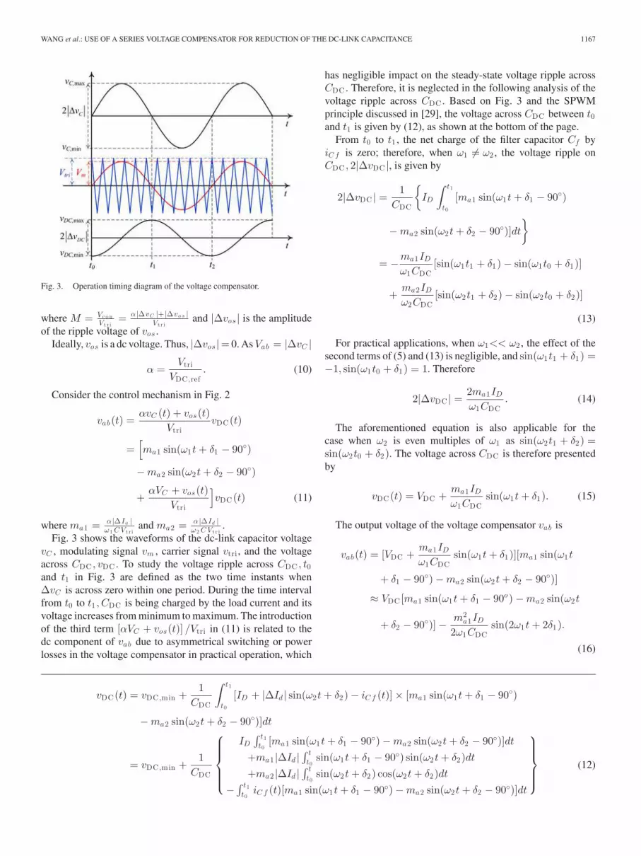
Fig. 3. Operation timing diagram of the voltage compensator.
where M = Vc o n
V t r i= α |∆vC |+ |∆vo s |
V t r iand |∆vos | is the amplitude
of the ripple voltage of vos .
Ideally, vos is a dc voltage. Thus, |∆vos |= 0. As Vab = |∆vC |
α =Vtri
VDC ,ref. (10)
Consider the control mechanism in Fig. 2
vab(t) =αvC (t) + vos(t)
VtrivDC(t)
=[
ma1 sin(ω1t + δ1 − 90)
− ma2 sin(ω2t + δ2 − 90)
+αVC + vos(t)
Vtri
]
vDC(t) (11)
where ma1 = α |∆Ia |ω1 C V t r i
and ma2 = α |∆Id |ω2 C V t r i
.
Fig. 3 shows the waveforms of the dc-link capacitor voltage
vC , modulating signal vm , carrier signal vtri , and the voltage
across CDC , vDC . To study the voltage ripple across CDC , t0and t1 in Fig. 3 are defined as the two time instants when
∆vC is across zero within one period. During the time interval
from t0 to t1 , CDC is being charged by the load current and its
voltage increases from minimum to maximum. The introduction
of the third term [αVC + vos(t)] /Vtri in (11) is related to the
dc component of vab due to asymmetrical switching or power
losses in the voltage compensator in practical operation, which
has negligible impact on the steady-state voltage ripple across
CDC . Therefore, it is neglected in the following analysis of the
voltage ripple across CDC . Based on Fig. 3 and the SPWM
principle discussed in [29], the voltage across CDC between t0and t1 is given by (12), as shown at the bottom of the page.
From t0 to t1 , the net charge of the filter capacitor Cf by
iC f is zero; therefore, when ω1 = ω2 , the voltage ripple on
CDC , 2|∆vDC |, is given by
2|∆vDC | =1
CDC
ID
∫ t1
t0
[ma1 sin(ω1t + δ1 − 90)
− ma2 sin(ω2t + δ2 − 90)]dt
= −ma1ID
ω1CDC[sin(ω1t1 + δ1) − sin(ω1t0 + δ1)]
+ma2ID
ω2CDC[sin(ω2t1 + δ2) − sin(ω2t0 + δ2)]
(13)
For practical applications, when ω1<< ω2 , the effect of the
second terms of (5) and (13) is negligible, and sin(ω1t1 + δ1) =−1, sin(ω1t0 + δ1) = 1. Therefore
2|∆vDC | =2ma1ID
ω1CDC. (14)
The aforementioned equation is also applicable for the
case when ω2 is even multiples of ω1 as sin(ω2t1 + δ2) =sin(ω2t0 + δ2). The voltage across CDC is therefore presented
by
vDC(t) = VDC +ma1ID
ω1CDCsin(ω1t + δ1). (15)
The output voltage of the voltage compensator vab is
vab(t) = [VDC +ma1ID
ω1CDCsin(ω1t + δ1)][ma1 sin(ω1t
+ δ1 − 90) − ma2 sin(ω2t + δ2 − 90)]
≈ VDC [ma1 sin(ω1t + δ1 − 90o) − ma2 sin(ω2t
+ δ2 − 90)] −m2
a1ID
2ω1CDCsin(2ω1t + 2δ1).
(16)
vDC(t) = vDC ,min +1
CDC
∫ t1
t0
[ID + |∆Id | sin(ω2t + δ2) − iC f (t)] × [ma1 sin(ω1t + δ1 − 90)
− ma2 sin(ω2t + δ2 − 90)]dt
= vDC ,min +1
CDC
⎧
⎪
⎪
⎪
⎨
⎪
⎪
⎪
⎩
ID
∫ t1
t0[ma1 sin(ω1t + δ1 − 90) − ma2 sin(ω2t + δ2 − 90)]dt
+ma1 |∆Id |∫ t
t0sin(ω1t + δ1 − 90) sin(ω2t + δ2)dt
+ma2 |∆Id |∫ t
t0sin(ω2t + δ2) cos(ω2t + δ2)dt
−∫ t1
t0iC f (t)[ma1 sin(ω1t + δ1 − 90) − ma2 sin(ω2t + δ2 − 90)]dt
⎫
⎪
⎪
⎪
⎬
⎪
⎪
⎪
⎭
(12)

1168 IEEE TRANSACTIONS ON POWER ELECTRONICS, VOL. 29, NO. 3, MARCH 2014
Fig. 4. Operations during the hold-up time. (a) Waveforms. (b) Circuit duringthe time interval [0, th1 ]. (c) Circuit during the time interval [th1 , th2 ].
The first term of (16) is used to cancel the dc-link voltage
ripple, while the second term is a double frequency ripple, gen-
erating voltage variation on vd . Thus, the voltage ripple of vd
is
2|∆vd | =m2
a1ID
ω1CDC. (17)
III. HOLD-UP TIME ANALYSIS OF THE DC-LINK MODULE
The hold-up times of the system with and without the pro-
posed module are compared in the following. After a loss of the
input power, the energy stored in the dc-link module (i.e., the
dc-link capacitor and the capacitor connected to the dc source)
will be solely delivered to the load. In the following analysis, the
hold-up time th is defined as the time duration between the start
of the supply outage (i.e., ia = 0) and the voltage vd reduces to
the minimum dc bus voltage Vd,min . Fig. 4(a) shows the timing
diagram of two consecutive hold-up intervals distinguished by
the value of the modulation index M of the PWM modulator
in Fig. 1. Fig. 4(b) and (c) shows the equivalent circuits of the
two intervals [0,th1] and [th1 , th2], respectively. For the sake of
simplicity in the analysis, the power loss of the voltage com-
pensator is neglected and the dc-link module is connected to a
constant power load PL .
1) Initial state (t = 0) Consider the worst case scenario.
The voltage across the dc-link capacitor at the supply outage
time (i.e., t = 0) is vC (0) = VC − |∆vC |. The voltage across
CDC , vDC(0), equals VDC ,ref . The voltage ripple across the dc-
link capacitor is fully compensated by vab , implying
vab(0) = |∆vC | = MvDC(0) (18)
where M = α |∆vC (0)|V t r i
.
2) Stage I [0, th1] − M ≤ 1: th1 is the time instant at which
M = 1. Thus
α∆vC (th1)
Vtri= 1 (19)
vab(th1) = ∆vC (th1) = −vDC(th1). (20)
Based on (18)–(20)
∆vC (th1) = vDC(0) (21)
vd(th1) = VC − ∆vC (th1) − vab(th1)
= VC − vDC(0) + vDC(th1). (22)
In this stage, the variation of vd is small. Thus, the current idis assumed to be constant and is equal to ID . Thus
∆vC (th1) = |∆vC | +ID
Cth1 = vDC(0) (23)
and
th1 =C
ID[vDC(0) − |∆vC |] =
β
ω(γ − 1). (24)
By applying the conservation of energy between the energy
delivery from the whole dc-link module and the load consump-
tion
1
2Cv2
C (0) +1
2CDCv2
DC(0) −1
2Cv2
C (th1)
−1
2CDCv2
DC(th1) = PL th1 . (25)
Based on (25)
vDC(th1) = µ√
γ2 − λ(γ2 − 1)VC . (26)
By substituting (26) into (22)
vd(th1) = VC + µ√
λ + (1 − λ)γ2VC − vDC(0)
= [1 + µ√
γ2 − λ(γ2 − 1) − µγ]VC . (27)
3) Stage II [th1 , th2]: In this stage, the capacitors C and CDC
are connected in series. At th2 , the output voltage vd(th2) =Vd,min = ρVC . The final voltages across C and CDC can be

WANG et al.: USE OF A SERIES VOLTAGE COMPENSATOR FOR REDUCTION OF THE DC-LINK CAPACITANCE 1169
expressed as
∆vC (th2) = ∆vC (th1) +Ca
Ca + C[vd(th1) − vd(th2)]
= ∆vC (th1) + ∆xVC (28)
vDC(th2) = vDC(th1) −C
Ca + C[vd(th1) − vd(th2)]
= ∆vC (th1) − λ∆xVC (29)
where ∆x = 11+λ
(1 − ρ) − µ[γ −√
γ2 − λ(γ2 − 1)].
By applying the conservation of energy
1
2Cv2
C (th1) +1
2CDCv2
DC(th1) −1
2Cv2
C (th2)
−1
2CDCv2
DC(th2) = PL (th2 − th1). (30)
It can be derived from (30) that
th2 − th1 =β
ω
(
ρ
µ∆x +
1 + λ
2µ∆x2
)
. (31)
Based on (24) and (31), the hold-up time th and the number
of hold-up cycle N are
th =β
ω
(
ρ
µ∆x +
1 + λ
2µ∆x2 + γ − 1
)
(32)
N =β
2π
(
ρ
µ∆x +
1 + λ
2µ∆x2 + γ − 1
)
. (33)
The hold-up time of the dc link with only a capacitor bank
storing the same amount of energy is derived as follows. Let the
corresponding dc-link capacitance required, the hold-up time,
and hold-up cycle be C ′, t′h , and N ′ respectively. Thus, for the
same amount of energy stored in C ′ as with the dc-link module
C ′ =CV 2
C + CDCv2DC(0)
V 2C
=
(
1 +γ2µ2
λ
)
C. (34)
By assuming that the ripple currents following through the
dc-link capacitors with and without the voltage compensator are
the same
µ′ =∆v′
C
VC=
βID
ωC ′VC. (35)
Hence, by using (34) and (35)
t′h =C ′[VC − ∆vC (0)]2 − C ′(ρVC )2
2PL
=β
ω
(λ + γ2µ2)[(1 − λµλ+γ 2 µ2 )2 − ρ2 ]
2λµ(36)
N ′ =β
2π
(λ + γ2µ2)[(1 − λµλ+γ 2 µ2 )2 − ρ2 ]
2λµ. (37)
Equations (32), (33), (36), and (37) will be used to compare
the hold-up time with and without the proposed dc-link module.
The design guidelines will be given in the next section.
Fig. 5. Energy stored and instantaneous power handled by the dc-linkcapacitor.
IV. DESIGN GUIDELINES FOR THE DC-LINK MODULE
The design guidelines for applications with and without hold-
up time requirements are given below.
A. Applications Without Hold-Up Time Requirement
Some applications, like electronic ballasts, do not have the
hold-up time requirement. The dc-link module is used to bal-
ance the input and output power difference, and reduce the
dc-link voltage ripple. Fig. 5 shows the energy storage E and
instantaneous power p of the dc-link capacitor. The dc compo-
nent of energy E1 maintains a certain level of dc-link voltage.
Only the ac component of E requires the power p for balancing
the input and output power of the entire system. Therefore, with
the proposed dc-link module, the energy storage elements are
divided into two parts: one is stored in the reduced dc-link ca-
pacitor and the other one is stored in the voltage compensator.
The theoretical minimum energy storage required is Emin . In
the practical design, the overall energy storage of the dc-link
module is reduced to a certain level between E1 and Emin , for
example, E2 as illustrated in Fig. 5.
The reduction of the dc-link capacitance is limited by the
voltage stresses on the dc source capacitor and switching devices
in the module. Assume that the load current id is constant in the
module. Based on (5), the dc-link capacitor current iC equals
∆ia . Thus
iC = CdvC
dt= ∆ia ⇒ C|∆vC | = constant. (38)
The product of the dc-link capacitance and its peak ripple
voltage is a constant. Thus, the minimum value of vDC equals
|∆vC |. Fig. 6 shows the relationship between the value of Cand vDC . Without the dc-link module, it requires a capacitance
of Cnorm for meeting the design specification. Practically, the
chosen value for C is larger than Cnorm in order to sustain
the ripple current stress. Due to the aging effect of the capacitor
changing from Cnorm to C ′norm , the peak-to-peak dc-link voltage
ripple will increase from 2|∆vC,norm | to 2|∆v′C,norm |.

1170 IEEE TRANSACTIONS ON POWER ELECTRONICS, VOL. 29, NO. 3, MARCH 2014
Fig. 6. Relationship between the dc-link capacitance, ripple voltage, and vDC .
The design of the dc-link capacitance value C with the dc-
link module is a compromise among the allowable voltage level
of vDC , and the stress on the capacitor CDC and the MOS-
FETs S1 − S4 . A smaller value of C requires higher voltage
ratings of CDC and S1 − S4 . Moreover, a boundary capacitance
Cbd can be determined based on specifications of power elec-
tronic systems, availability, cost, and volume of different types
of capacitors. It provides a guideline on the selection of capac-
itor type. For instance, power film capacitors can be applied in
Choice 1 with a higher dc voltage on CDC , VDC ,1 , as compared
to that of Choice 2 with lower voltage VDC ,2 in which E-Caps
are used. Thus, with the aid of the dc-link module, the required
dc-link capacitance can be reduced, making it possible to use
capacitor of long lifetime, like power film capacitors, to ensure
the lifetime of the entire power electronic system, or extend the
performance lifetime even if there is a significant reduction in
the capacitance of the dc-link capacitor due to the aging effect.
The value of CDC is determined by using (17) to limit the
voltage ripple of vd . In the application example (a power factor
corrector (PFC) front-end stage plus a dc–dc converter) dis-
cussed in Section V, with conventional E-Cap solution (without
the voltage compensator)
2|∆vC | =2ID
ω1Cnorm. (39)
According to (17) and (39), as ma1 ≤ 1, the voltage ripple
across the output terminal of the dc-link module can be lim-
ited to lower than the one with conventional E-Cap solution by
choosing CDC no less than half of the capacitance of the E-Cap,
i.e.,
CDC ≥1
2Cnorm (40)
As the capacitor CDC withstands a low voltage stress, there
are several choices in the practical implementation. One choice
is to use low voltage E-Caps with high ripple current and long
lifetime. Unlike the ones with high voltage ratings, they are
available and cost-effective. Another choice is to use ceramic
capacitor tank or low-voltage film capacitors.
Fig. 7. Hold-up time analysis with and without the dc-link module (β = 1,ρ = 0.8, and µ = 0.02).
Fig. 8. Design curves for selection of λ and γ (ρ = 0.8, µ = 0.02).
B. Applications With Hold-Up Time Requirement
For this type of applications, the determining factor for the
energy storage is the required hold-up time rather than the volt-
age ripple specification. The design guidelines discussed are
based on the analysis in Section III.
Figs. 7 and 8 show the graphical representations of (33) and
(37) with β = 1 (the amplitude of the dc-link capacitor ripple
current is equal to the value of the average load current), ρ =0.8 (Vd,min is 80% of the dc-link voltage prior to the supply
outage), and µ = 0.02 (dc-link ripple voltage is 2% of the
average dc-link voltage). It should be noted in the comparison
that the factors λ and γ are for the proposed dc-link module
containing an additional energy storage capacitor CDC . They
appear in (37) as the comparison is based on the same energy
storage. As depicted in Fig. 7, with proper choices of λ (ratio
between C and CDC) and γ (ratio between vDC and |∆vC |),the number of hold-up cycles with the dc-link module can be
increased. The shaded area of the λ – γ selection curves shown in
Fig. 8 represents an extended hold-up time (i.e., N /N’ > 1). That
means, with the same amount of energy storage in the dc link,

WANG et al.: USE OF A SERIES VOLTAGE COMPENSATOR FOR REDUCTION OF THE DC-LINK CAPACITANCE 1171
Fig. 9. Experimental test bed. (a) System configuration. (b) Circuit schematic of the proposed module.
the hold-up time with the dc-link module is longer than using
a dc-link capacitor only. Different curves showing the constant
number of the hold-up cycles and N/N ′ ratios are plotted in dot
lines and solid lines, respectively.
The illustrations given in Figs. 7 and 8 are with µ = 0.02,
which is corresponding to a determined value of the dc-link
capacitance C from the design perspective. Therefore, the trade-
off design condition is between maximization of N/N ′ and
minimization of CDC and its voltage stress vDC , meanwhile,
achieving the required hold-up cycle N . Different figures can
be plotted for other values of µ, corresponding to different values
of C. By considering all of the values of λ and γ selected for
different value of µ, it allows the selection of the optimal values
of µ, λ, and γ. Thus, the optimal values of C,CDC , and vDC are
selected.
V. EXPERIMENTAL VERIFICATIONS
An experimental ac–dc–dc converter test bed as shown
in Fig. 9(a) has been built. It is constructed by connecting
a 3-kW PFC—STMicroelectronics STEVAL-ISF001V1 to a
600 W phase-shifted FB dc–dc converter—Texas Instruments
UCC28950EVM-442. An input LC filter composed of 1.47-µF
film capacitors (1 and 0.47 µF in parallel) and a 20-µH inductor
is applied to smooth the input current id . The detailed circuit
and operation of the phase-shifted FB dc–dc converter are dis-
cussed in [30] except for that the 330-µF input capacitor in the
evaluation board is removed in the experiments. The PFC is sup-
plied by an AC power source Kikusui PCR2000LA. The supply
voltage is 220 V, 50 Hz. The output of the dc–dc converter is
connected to an electronic load Kikusui PLZ1003W.The rated
output voltage of the dc–dc converter is 12 V. The output

1172 IEEE TRANSACTIONS ON POWER ELECTRONICS, VOL. 29, NO. 3, MARCH 2014
Fig. 10. Experimental waveforms with an electrolytic capacitor bank. (a)Startup transient under the full-load condition (vC : 100 V/div, Time base:50 ms/div). (b) Steady-state dc-link voltage waveform under the full-load con-dition (∆vC : 2 V/div, Time base: 10 ms/div). (c) Transient waveforms when theoutput is changed from 10% load to full load (vC : 100 V/div, iout : 50 A/div,Time base: 50 ms/div). (d) Transient waveforms when the output is changed fromfull load to 10% load. (vC : 100 V/div, iout : 50 A/div, Time base: 50 ms/div). (e)Transient waveforms after a sudden supply outage under the full-load condition.(vC :100 V/div, vS : 300 V/div, iout : 20 A/div, Time base: 10 ms/div).
TABLE I
VALUES OF THE COMPONENTS USED IN THE MODULE
capacitor bank C in the PFC is formed by connecting two
330 µF, 450 V E-Cap capacitors in parallel. According to
the manufacturer’s datasheet, the lifetime of the capacitors is
3000 h at 105 C (12 000 h estimated at 85 C and rated ripple
current). Fig. 10(a) and (b) shows the startup transient and
steady-state waveform of vC when the output is full load. The
average dc voltage is 400 V and peak-to-peak ac ripple voltage
(i.e., ∆vC ) is 10.8 V. The settling time of the startup process is
150 ms. Fig. 10(c) shows the output current iout and vC when
the output is suddenly changed from 10% load to full load. vC
is momentarily dropped by 45 V and the settling time is 100 ms.
Fig. 10(d) shows the corresponding waveforms when the output
is suddenly changed from full load to 10% load. vC is momen-
tarily jumped up by 37.7 V and the settling time is 150 ms.
Fig. 10(e) shows the waveforms of vC , PFC input voltage vS ,
and output current iout when vS is suddenly turned off. vC re-
duces to 320 V (80% of 400 V) after 24.6 ms. Within this period,
the dc–dc converter is still in normal operation. The measured
steady-state RMS value of capacitor current and ESR of the ca-
pacitor bank is 1.7 A and 130 mΩ, respectively. Thus, the total
power loss of the capacitor bank is estimated to be 0.38 W at
full load.
The E-Cap bank is replaced by the proposed module. The cir-
cuit schematic of the module is shown in Fig. 9(b). The power
stage design of the voltage compensator follows the way to de-
sign a typical FB inverter as discussed in [29]. The input voltage
level of the voltage compensator is selected according to the dc-
link capacitance (as shown in Fig. 6) and the modulation index
of the SPWM controller. In the prototype, the modulation index
is 0.5 under full-load condition to achieve a sufficient robustness
margin and avoid over modulation. The dc-link capacitance is
120 µF (in the case without hold-up time requirement) with a
peak-to-peak voltage ripple of about 50 V. Thus, the input volt-
age vDC is regulated at 50 V by setting a 5 V reference in the
control stage. The switching frequency of the voltage compen-
sator is 50 kHz. Components used in the power conversion stage
and the key design parameters are listed in Table I. Two design
cases are investigated. The first design has no hold-up time re-
quirement, while the second one has the hold-up requirement.
They are discussed as follows.
A. Without Hold-Up Time Requirement
A 120-µF (82% capacitance reduction) film capacitor with the
lifetime of 100 000 h at 85 C and rated ripple current is used to

WANG et al.: USE OF A SERIES VOLTAGE COMPENSATOR FOR REDUCTION OF THE DC-LINK CAPACITANCE 1173
Fig. 11. Experimental waveforms with the proposed dc-link module. (a) Start-up transient under the full-load condition. (vd : 100 V/div, Time base: 50 ms/div).(b) Steady-state waveforms of vC and vd under the full-load condition (∆vC : 20 V/div, ∆vd : 2 V/div, Time base: 10 ms/div). (c) Transient waveforms ofthe dc-link module when the output is changed from 10% load to full load (vd : 100 V/div, vC : 100 V/div, va b : 40 V/div, id : 2 A/div, Time base: 50 ms/div).(d) Transient waveforms of the FB dc–dc converter when the output is changed from 10% load to full load (vd : 100 V/div, id : 2 A/div, vout : 10 V/div, iout : 50A/div, Time base: 50 ms/div). (e) Transient waveforms of the dc-link module when the output is changed from full load to 10% load (vd : 100 V/div, vC : 100 V/div,va b : 40 V/div, id : 2 A/div, Time base: 50 ms/div). (f) Transient waveforms of the FB dc–dc converter when the output is changed from full load to 10% load (vd :100 V/div, id : 2 A/div, vout : 10 V/div, iout : 50 A/div, Time base: 50 ms/div). (g) Transient waveforms after a sudden supply outage under the full-load condition(vd :100 V/div, vS : 300 V/div, va b : 20 V/div, iout : 50 A/div, Time base: 10 ms/div).
replace the capacitor bank. A 1000-µF, 63-V low-voltage E-Cap
with the lifetime of 8000 h at 125 C (128 000 h estimated at
85 C and rated ripple current, which is comparable with the
lifetime of the film capacitor) is used for the module, i.e., CDC .
The voltage across CDC is designed to be 50 V. Fig. 11(a) shows
the startup transient of the module output vd . The dc value of
vd is 400 V. The settling time of the startup process is 75 ms.
Fig. 11(b) shows the steady-state waveforms of the capacitor
ripple voltage ∆vC and module output ripple voltage ∆vd , when
the output is at full load. Their peak-to-peak ripple voltages

1174 IEEE TRANSACTIONS ON POWER ELECTRONICS, VOL. 29, NO. 3, MARCH 2014
are 49.1 and 3.9 V, respectively. Fig. 11(c) and (d) shows the
transient waveforms of vd , vC , module output voltage vab , input
current of the FB dc–dc converter id , output voltage of the dc–dc
converter vout and output current of the dc–dc converter iout ,
when the output is suddenly changed from 10% load to full
load. vd is momentarily reduced by 45.5 V and its settling time
is 100 ms. Fig. 11(e) and (f) shows the corresponding waveforms
when the output is suddenly changed from full load to no load.
vd is momentarily increased by 37.7 V and its settling time is
150 ms. Comparing Fig. 10(a) with Fig. 11(a), and Fig. 10(b)
with Fig. 11(b), the startup time is shorter and the ripple voltage
is smaller with the proposed module. As shown in Fig. 10(c) and
(d), and Fig. 11(c) and (e), under the load change conditions, the
transient responses of the system with the module are similar
to the ones with the E-Cap bank. The total power dissipation
of the module is around 1.5 W. From the perspective of the
capacitor lifetime at 85 C with a same ripple current design
margin, the proposed module is estimated to have a lifetime
more than eight times of that of the E-Caps without the voltage
compensator.
B. With Hold-Up Time Requirement
The module is designed to achieve the same hold-up time
with the electrolytic capacitors. Based on the design method de-
scribed in Section IV, a 450-µF capacitor (32% capacitancere-
duction) is used for C and a 1000-µF, 63-V low-voltage elec-
trolytic capacitors for CDC , corresponding to an overall energy
storage of 72% of that with E-Caps solution without the voltage
compensator. Fig. 11(g) shows the waveforms of vd , vS , vab ,
and iout after vS is suddenly turned off under the full-load
condition. Comparing Fig. 10(e) with Fig. 11(g), the proposed
module gives a similar hold-up performance to the electrolytic
capacitor bank with 28% energy storage reduction.
Thus, the experimental results reveal that the proposed dc-
link module can reduce the required capacitance value for the
dc-link capacitor without sacrificing the transient and steady-
state responses of the whole system. Although the proposed
module requires capacitors as the dc source, the voltage level is
only 50 V, allowing the use of low-voltage capacitors of long
lifetime. The only drawback is that there is an increase in the
overall power loss by 1.12 W.
From the practical point of view, the use of E-Caps is still the
low-cost solution. Then, even if the E-Cap bank is unchanged
in the application, the proposed module allows a wide range
of reduction in the dc-link capacitance (due to aging effect)
without sacrificing the performance. For applications without
the hold-up requirement, it allows the reduction of the dc-
link capacitance from 660 to 120 µF in the test. For appli-
cations with the hold-up time requirement, the module allows
the reduction from 660 to 450 µF and 28% reduction of the
overall energy storage in the dc-link module. The resulting ef-
fect will extend the life expectancy of the entire system from
the perspective of reducing the chance of system failure due
to aging of the dc-link capacitors. The proposed method has
a distinct advantage for high-voltage applications, due to the
fact that the voltage rating of power film capacitors is usu-
ally higher than that of E-Caps. With the proposed module,
the dc-link capacitance can be reduced and a fewer number
of high-voltage power film capacitors are used to replace the
E-Caps.
VI. CONCLUSION
An active series voltage compensator for reducing the dc-link
capacitance in a capacitor-supported power electronic system
has been proposed. The implementation requires low-voltage
devices only, as the dc-link module only handles ripple voltage
in the dc-link and reactive power flow in the dc link. A detailed
study on the dc and ac characteristics, stability analysis, and
hold-up time performance has been given. The design guidelines
for the dc-link module for applications with and without the
hold-up time requirement have been described. The proposed
method has been demonstrated on a two-converter system with
the front-stage power factor corrector and second-stage of a dc–
dc converter. The performances with the capacitor bank only
and the proposed dc-link module have also been compared.
APPENDIX
A. Proof of (6)
Based on (4) and (5), (6) is derived as follows:
Pab =1
T
∫ T
0
vab(t) [∆id(t) + ID ] dt
=1
T
∫ T
0
vab(t)∆id(t)dt + 0
=1
T
∫ T
0
[
|∆Ia |
ω1Csin(ω1t + δ1 − 90o) −
|∆Id |
ω2C
× sin(ω2t + δ2 − 90o)
]
|∆Id | sin(ω2t + δ2)dt
=|∆Id ||∆Ia |
2ω1CT
∫ T
0
sin[(ω1 − ω2)t + (δ1 − δ2)]
− sin[(ω1 + ω2)t + (δ1 + δ2)]dt − 0
=|∆Id ||∆Ia |
2ω1CT
∫ T
0
sin[(ω1 − ω2)t + (δ1 − δ2)]dt
−|∆Id ||∆Ia |
2ω1CT
∫ T
0
sin[(ω1 + ω2)t + (δ1 + δ2)]dt
=|∆Id ||∆Ia |
2ω1CT
∫ T
0
sin[(ω1 − ω2)t + (δ1 − δ2)]dt − 0
=|∆Id ||∆Ia |
2ω1CT
∫ T
0
sin[(ω1 − ω2)t + (δ1 − δ2)]dt.
REFERENCES
[1] G. Terzulli, “Film technology to replace electrolytic technology in windpower applications,” AVX Tech. Note 2010.
[2] EPCOS AG, Munich, Germany, “Film capacitors for industrial applica-tions,” Edition 04.07, 2007.

WANG et al.: USE OF A SERIES VOLTAGE COMPENSATOR FOR REDUCTION OF THE DC-LINK CAPACITANCE 1175
[3] X. Chen and M. Kazerani, “Space vector modulation control of an AC-DC-AC converter with a front-end diode rectifier and reduced DC-linkcapacitor,” IEEE Trans. Power Electron., vol. 21, no. 5, pp. 1470–1478,Sep. 2006.
[4] C. R. Neuhaus and R. W. D. Doncker, “DC-link voltage control forswitched reluctance drives with reduced DC-link capacitance,” in Proc.IEEE Energy Convers. Congr. Expo., 2010, pp. 4192–4198.
[5] D. Lamar, J. Sebastian, M. Arias, and A. Fernandez, “On the limit of theoutput capacitor reduction in power-factor correctors by distorting the lineinput current,” IEEE Trans. Power Electron., vol. 27, no. 3, pp. 1168–1176,Mar. 2012.
[6] P. Pelletier, J. M. Guichon, J. L. Schanen, and D. Frey, “Optimization ofa DC capacitor tank,” IEEE Trans. Ind. Appl., vol. 45, no. 2, pp. 880–886,Mar./Apr. 2009.
[7] P. W. Hammond, “Control method and apparatus to reduce current throughDC capacitor linking two static converters,” U.S. Patent 6 762 947, Jul.13, 2004.
[8] G. Kalman and C. Huggett, “AC-to-AC power converter without a DClink capacitor,” U.S. Patent 6 839 249, Jan. 4, 2005.
[9] B. G. Gu and K. Nam, “A DC-link capacitor minimization method throughdirect capacitor current control,” IEEE Trans. Ind. Appl., vol. 42, no. 2,pp. 573–581, Mar./Apr. 2006.
[10] I. S. Freitas, C. B. Jacobina, and E. C. Santos, “Single-phase to single-phase full-bridge converter operating with reduced AC power in the DC-link capacitor,” IEEE Trans. Power Electron., vol. 25, no. 2, pp. 272–279,Feb. 2010.
[11] T. Okuda, T. Urakabe, and Y. Kuramoto, “Motor driving apparatus,” U.S.Patent 7 310 475, Dec. 18, 2007.
[12] H. Song, D. Oh, K. Nam, and S. Kim, “Method for controlling voltage ofDC-link for electric vehicle,” U.S. Patent 7 528 566, May 5, 2009.
[13] J. Ying, Q. Zhang, A. Qiu, T. Liu, X. Guo, and J. Zeng, “DC-DC convertercircuits and method for reducing DC-bus capacitor current,” U.S. Patent7 009 852,” Mar. 7, 2006.
[14] D. C. Hamill and P. T. Krein, “A ‘zero’ ripple technique applicable toany DC converter,” in Proc. IEEE Power Electron. Spec. Conf., 1999,pp. 1165–1171.
[15] B. K. Bose and D. Kastha, “Electrolytic capacitor elimination in powerelectronic system by high frequency active filter,” in Proc. IEEE Ind. Appl.Soc. Annu. Meet., 1991, pp. 869–878.
[16] P. E. Nuechterlein, “DC-link ripple reduction circuit,” U.S. Patent5 014 177, May 7, 1991.
[17] Y. Wang, G. Joos, and H. Jin, “DC-side shunt-active power filter for phase-controlled magnet-load power supplies,” IEEE Trans. Power Electron.,vol. 12, no. 5, pp. 765–771, Sep. 1997.
[18] T. Shimizu, Y. Jin, and G. Kimura, “DC ripple current reduction ona single-phase PWM voltage-source rectifier,” IEEE Trans. Ind. Appl.,vol. 36, no. 5, pp. 1419–1429, Sep./Oct. 2000.
[19] O. Garcia, M. D. Martinez-Avial, J. A. Cobos, J. Uceda, J. Gonzalez, andJ. A. Navas, “Harmonic reducer converter,” IEEE Trans. Ind. Electron.,vol. 50, no. 2, pp. 322–327, Apr. 2003.
[20] D. Zhou, “Reduced capacitance AC/DC/AC power converter,” U.S. Patent6 804 127, Oct. 12, 2004.
[21] C. Kyritsis, N. P. Papanicolaou, and E. C. Tatakis, “A novel parallel activefilter for current pulsation smoothing on single stage grid-connected AC-PV modules,” in Proc. Eur. Conf. Power Electron. Appl., 2007, pp. 1–10.
[22] S. G. Li, B. Ozpineci, and L. M. Tolbert, “Evaluation of a current sourceactive power filter to reduce the DC bus capacitor in a hybrid electricvehicle traction drive,” in Proc. IEEE Energy Convers. Congr. Expo.,2009, pp. 1185–1190.
[23] H. Yoo and S. K. Sul, “A new circuit design and control to reduce inputharmonic current for a three-phase AC machine drive system having avery small DC-link capacitor,” in Proc. IEEE Appl. Power Electron. Conf.,2010, pp. 611–618.
[24] R. X. Wang, F. Wang, D. Boroyevich, R. Burgos, R. X. Lai, P. Q. Ning,and K. Rajashekara, “A high power density single-phase PWM rectifierwith active ripple energy storage,” IEEE Trans. Power Electron., vol. 26,no. 5, pp. 1430–1443, May 2011.
[25] H. B. Li, K. Zhang, and H. Zhao, “Active DC-link power filter for singlephase PWM rectifiers,” in Proc. IEEE Int. Conf. Power Electron. ECCEAsia, 2011, pp. 2920–2926.
[26] X. Du, L. W. Zhou, H. Lu, and L. M. Tai, “DC link active power filterfor three-phase diode rectifier,” IEEE Trans. Ind. Electron., vol. 59, no. 3,pp. 1430–1442, Mar. 2012.
[27] P. Krein, R. Balog, and M. Mirjafari, “Minimum energy and capacitancerequirements for single-phase inverters and rectifiers using a ripple port,”IEEE Trans. Power Electron., vol. 27, no. 11, pp. 4690–4698, Nov. 2012.
[28] H. Hu, S. Harb, N. H. Kutkut, Z. J. Shen, and I. Batarseh, “A single-statemicroinverter without using electrolytic capacitors,” IEEE Trans. PowerElectron., vol. 28, no. 6, pp. 2677–2687, Jun. 2013.
[29] N. Mohan, T. M. Undeland, and W. P. Robbins, Power Electronics, Con-verters, Applications, and Design. New York, NY, USA: Wiley, 2003,ch. 8.
[30] Texas Instruments, Dallas, TX, USA, “600-W phase-shifted full-bridgeconverter,” User’s Guide SLUU421A, May 2010.
Huai Wang (S’07–M’12) received the B.Eng. de-gree in electrical and electronic engineering fromthe Huazhong University of Science and Technol-ogy, Wuhan, China, in 2007, and the Ph.D. degreein electronic engineering from the City University ofHong Kong, Kowloon, Hong Kong, in 2012.
Since 2012, he has been with Aalborg University,Aalborg, Denmark, where he is currently an AssistantProfessor in the Department of Energy Technology,working at the Center of Reliable Power Electronics.From April to September 2010, he was an intern stu-
dent at ABB Corporate Research Center, Switzerland. From November 2007 toDecember 2008, he was a Research Assistant at the Centre for Power Electron-ics, City University of Hong Kong. He has authored or coauthored more than 30technical papers and filed three patents. His research interests include reliabilityof capacitors for dc-link application, reliability of power electronic systems,high-voltage dc–dc power converters, fast dynamic control of converters, andpassive components reduction technology.
Dr. Wang is the recipient of several paper awards and project awards fromindustry, IEEE, and the Hong Kong Institution of Engineers. He is currently acommittee member of the IEEE Power Electronics Society Technical Commit-tee on High Performance Emerging Technologies.
Henry Shu-Hung Chung (M’95–SM’03) receivedthe B.Eng. and Ph.D. degrees in electrical engineer-ing both from The Hong Kong Polytechnic Univer-sity, Hong Kong, in 1991 and 1994, respectively.
Since 1995, he has been with the City Universityof Hong Kong, Kowloon, Hong Kong, where he iscurrently a Professor in the Department of ElectronicEngineering, and the Director of the Centre for SmartEnergy Conversion and Utilization Research. He hasauthored six research book chapters, and more than300 technical papers including 140 refereed journal
papers in his research areas, and holds 26 patents. His research interests includetime- and frequency-domain analysis of power electronic circuits, switched-capacitor-based converters, random-switching techniques, control methods, dig-ital audio amplifiers, soft-switching converters, and electronic ballast design.
Dr. Chung is currently the Chairman of the Technical Committee on High-Performance and Emerging Technologies of the IEEE Power Electronics Soci-ety, and an Associate Editor of the IEEE TRANSACTIONS ON POWER ELECTRON-ICS, the IEEE TRANSACTIONS ON CIRCUITS AND SYSTEMS, PART I: FUNDAMEN-TAL THEORY AND APPLICATIONS, and the IEEE JOURNAL OF EMERGING AND
SELECTED TOPICS IN POWER ELECTRONICS.
Wenchao Liu received the B.Sc. and M.Sc. degreesin electrical and electronics engineering from theHuazhong University of Science and Technology,Wuhan, China, in 2007 and 2009, respectively.
From 2009 to 2011, he was with Delta Electron-ics (Shanghai) Co., Ltd., as an Electronics Engineerin the Network & Telecom Power Department. Heis currently a Senior Research Assistant with theCentre for Smart Energy Conversion and UtilizationResearch, City University of Hong Kong, Kowloon,Hong Kong. His research interests include electric
energy storage systems, control of power converters, and renewable energyapplication.