Embed Size (px)
Citation preview
System on Chip PIC16F84 on FPGA Xilinx
Using CQPIC Soft ProcessorLast update : 2010-09-10
Serge Moutou
Institut Universitaire de Technologie - Genie Électrique et Informatique Industrielle 9, rue de Québec - BP 396 - 10026 TROYES cedex France
Key words : softcore processor, SoC (System On Chip), C programming language and FPGA, FPGA Spartan3, Digilent Starter Board, VGA monitor, PIC®16F84
The starting VHDL core and its last modifications are in :"http://moutou.pagesperso-orange.fr/ER2/CQPICStart.zip".
IntroductionThe goal of this project is to construct a pong game interfaced to a VGA monitor with FPGA as a target chip. The pong game on VGA and on a FPGA is a classical subject and you can find a lot of examples on the Internet. But our goal is to use a free 8-bit soft processor interacting with external hardware described in VHDL. The soft core which we refer to as CQPIC in this document, is compatible with the Microchip famous PIC®16F84. We expect to program this soft core with C language.
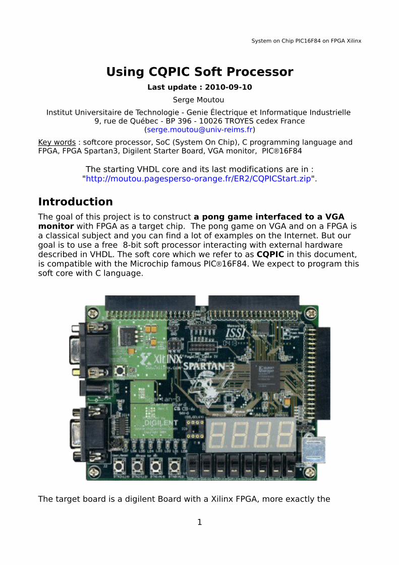
The target board is a digilent Board with a Xilinx FPGA, more exactly the
1
System on Chip PIC16F84 on FPGA Xilinx
Spartan-3 Starter Board see :
http://www.digilentinc.com/Products/Catalog.cfm?NavPath=2,400&Cat=10
Integrated Development Environment (IDE) used are then :
- ISE Xilinx for VHDL programs or the free WebPack (http://www.xilinx.com/support/download/).
- MPLAB (http://www.microchip.com/stellent/idcplg?IdcService=SS_GET_PAGE&nodeId=1406&dDocName=en019469) for developing 8-bit PIC1657 applications in Windows NT/2000/XP/Vista/7 environments and using assembler or Hi-Tech C (http://www.htsoft.com/). Hi-Tech C is free for a lite version when installing MPLAB.
This project is intended for two undergraduate students in third semester during 80 hours.
The CQPIC is a free soft core (or soft processor) able to run the same instructions as microchip PIC® 16F84. Because this project is removed from OpenCores.org and then difficult to find, you can download my new version in the internet "http://perso.wanadoo.fr/moutou/ER2/CQPICStart.zip".
It was developped by Sumio Morioka (Japan) and published in December 1999 in "Transistor Gijutsu Magazine" (its last update was in 2004)
Where do we start or choosing a CoreAt means three versions of compatible PIC® 16F84 soft processor can be found in the internet. The most recent is probably a Verilog project available at opencores : "http://opencores.org/project,risc16f84" with recent updates (2006). But with undergraduate students who have only skills on VHDL, I intend to use CQPIC, older, but at the origin of this verilog core.
Last academic year, I have used and programmed a soft processor 16C57 and the corresponding report of the project is also available in the Internet "http://perso.wanadoo.fr/moutou/ER2/SiliCore1657_en.pdf". This old project, which we refer to as silicore1657 in the following, allows me to acquire experience useful for choosing the core. An other VHDL core is also available which we refer to as PPX in the following (http://opencores.org/project,ppx16) from Daniel Wallner, used and debugged by Patrice Nouel, Maître de Conférence in ENSIERB (now retired). But my choice is the CQPIC core because it doesn't use bidirectional PORTs but three PORTs as explained further in this document.
We first present the hardware core starting from Microchip documentation.
PIC® 16F84 ArchitectureIt is a 8-bit processor with a 14-bit wide instruction set. The original PIC 16F84 has a only 68 bytes wide RAM. An other limitation is its stack : only eight levels. It's probably very hard to program a C compiler with this architecture but we have one for free.
2
System on Chip PIC16F84 on FPGA Xilinx
This processor manage interrupts (only one interrupt vector but many sources of interrupts).
We begin with the more difficult part : the Register File. I use the word "difficult" only because of the memory banking, a microchip particularity even with more recent 8-bit microcontroller (till 18FXXX series) which only disapears with the new 16/32-bit architectures (24FXXX and others)
The register FileThe register file is broken up into two banks as presented below. The register bank is selected by modifying the one bank selection bit RP0 of the STATUS register. The lower thirdteen registers in each bank are sometimes different sometimes identical. The sixtyheight SRAM registers in each bank all map back to BANK 0.
General banked memory starts at 0x50 address and was not used in the 16F84.
File Address
Banque 0 Banque 1 File Address
00h Indirect addr. Indirect addr. 80h
bcf status,rp0 01h TMR0 OPTION_REG 81h bsf status,rp0
passe en 02h PCL PCL 82h passe en
banque 0 03h STATUS STATUS 83h banque 1
04h FSR FSR 84h
05h PORTA TRISA 85h
06h PORTB TRISB 86h
07h --- --- 87h
08h EEDATA EECON1 88h
09h EEADR EECON2 89h
0Ah PCLATH PCLATH 8Ah
0Bh INTCON INTCON 8Bh
0Ch 68 cases mémoires
SRAM
correspond à la banque 0
8Ch
...
4Fh CFh
3
System on Chip PIC16F84 on FPGA Xilinx
not used not used
7Fh FFh
You can also see the addresses 07h and 87h are not used in 16F84 but we will use them in our core as explained further.
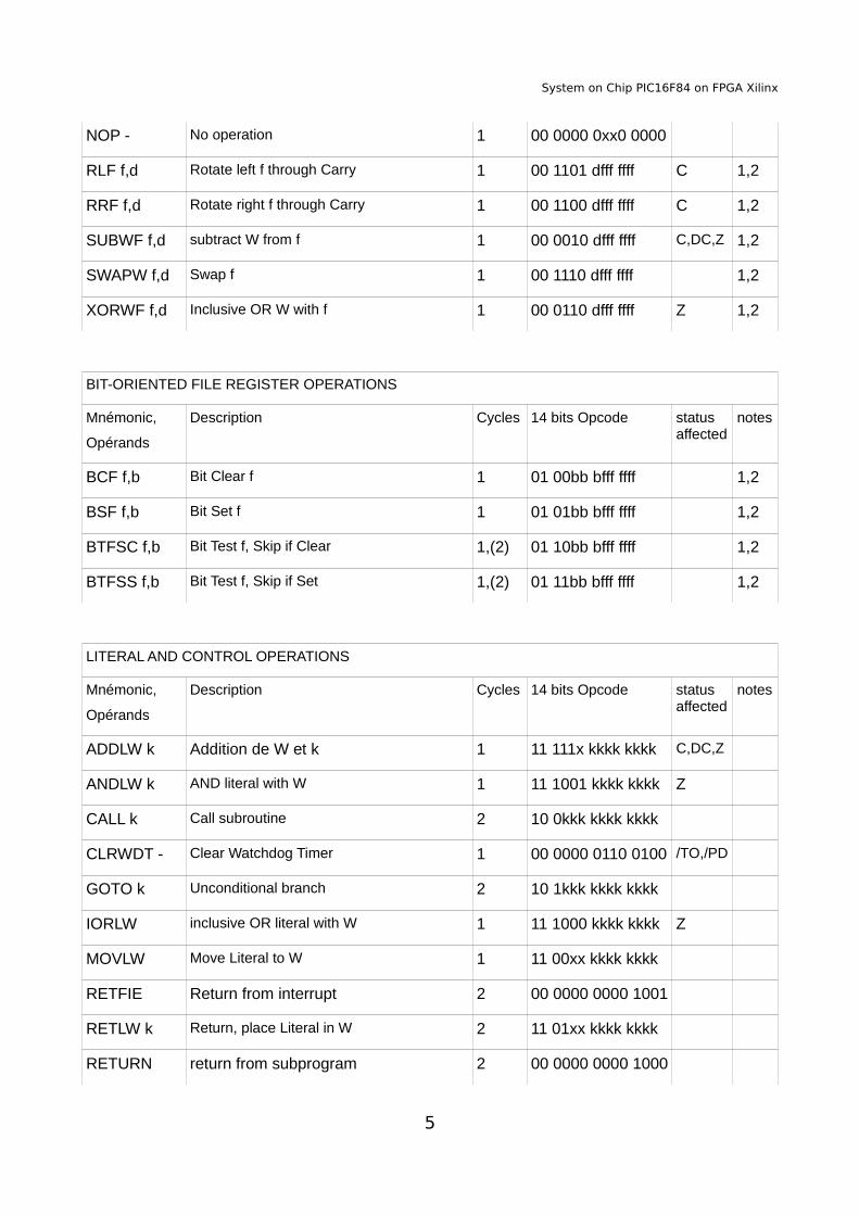
Instructions SetThe 35 instructions of PIC® 16F84 are now presented.
Operands :
- f : register file address from 00 to 7F- W : Working register (accumulator) - d : destination selection : d=0 store result in W , d=1 store result in f- bbb : Bit address within an 8-bit file register (3 bits)- k : Literal field, constant data or label (8, or 9 bits)- PC program counter- TO Time Out bit- PD Power Down bit
BYTE-ORIENTED FILE REGISTER OPERATIONS
Mnemonic
Operand
Description Cycles 14 bits Opcode status affected
notes
ADDWF f,d Add W and f 1 00 0111 dfff ffff C,DC,Z 1,2
ANDWF f,d AND W with f 1 00 0101 dfff ffff Z 1,2
CLRF f Clear f 1 00 0001 1fff ffff Z 2
CLRW - Clear W 1 00 0001 0xxx xxxx Z
COMF f,d Complement f 1 00 1001 dfff ffff Z 1,2
DECF f,d Decrement f 1 00 0011 dfff ffff Z 1,2
DECFSZ f,d Decrement f (skip if 0) 1,(2) 00 1011 dfff ffff Z 1,2,3
INCF f,d Increment f 1 00 1010 dfff ffff Z 1,2
INCFSZ f,d Increment f (skip if 0) 1,(2) 00 1111 dfff ffff Z 1,2,3
IORWF f,d Inclusive OR W with f 1 00 0100 dfff ffff Z 1,2
MOVF f,d Move f 1 00 1000 dfff ffff Z 1,2
MOVWF Move W to f 1 00 0000 1fff ffff
4
System on Chip PIC16F84 on FPGA Xilinx
NOP - No operation 1 00 0000 0xx0 0000
RLF f,d Rotate left f through Carry 1 00 1101 dfff ffff C 1,2
RRF f,d Rotate right f through Carry 1 00 1100 dfff ffff C 1,2
SUBWF f,d subtract W from f 1 00 0010 dfff ffff C,DC,Z 1,2
SWAPW f,d Swap f 1 00 1110 dfff ffff 1,2
XORWF f,d Inclusive OR W with f 1 00 0110 dfff ffff Z 1,2
BIT-ORIENTED FILE REGISTER OPERATIONS
Mnémonic,
Opérands
Description Cycles 14 bits Opcode status affected
notes
BCF f,b Bit Clear f 1 01 00bb bfff ffff 1,2
BSF f,b Bit Set f 1 01 01bb bfff ffff 1,2
BTFSC f,b Bit Test f, Skip if Clear 1,(2) 01 10bb bfff ffff 1,2
BTFSS f,b Bit Test f, Skip if Set 1,(2) 01 11bb bfff ffff 1,2
LITERAL AND CONTROL OPERATIONS
Mnémonic,
Opérands
Description Cycles 14 bits Opcode status affected
notes
ADDLW k Addition de W et k 1 11 111x kkkk kkkk C,DC,Z
ANDLW k AND literal with W 1 11 1001 kkkk kkkk Z
CALL k Call subroutine 2 10 0kkk kkkk kkkk
CLRWDT - Clear Watchdog Timer 1 00 0000 0110 0100 /TO,/PD
GOTO k Unconditional branch 2 10 1kkk kkkk kkkk
IORLW inclusive OR literal with W 1 11 1000 kkkk kkkk Z
MOVLW Move Literal to W 1 11 00xx kkkk kkkk
RETFIE Return from interrupt 2 00 0000 0000 1001
RETLW k Return, place Literal in W 2 11 01xx kkkk kkkk
RETURN return from subprogram 2 00 0000 0000 1000
5
System on Chip PIC16F84 on FPGA Xilinx
SLEEP Go into standby mode 1 00 0000 0110 0011 /TO,/PD
SUBLW k Go into standby mode 1 11 110x kkkk kkkk C,DC,Z
XORLW exclusive OR literal with W 1 11 1010 kkkk kkkk Z
Note 1: When an I/O register is modified as a function of itself ( e.g., MOVF PORTB, 1), the value used will be that value present on the pins themselves. For example, if the data latch is ’1’ for a pin configured as input and is driven low by an external device, the data will be written back with a ’0’. 2: If this instruction is executed on the TMR0 register (and, where applicable, d = 1), the prescaler will be cleared if assigned to the Timer0 Module. 3: If Program Counter (PC) is modified or a conditional test is true, the instruction requires two cycles. The second cycle is executed as a NOP.
Create your own microcontroller with the CQPIC.The CQPIC is delivered as a VHDL soft core module, and is intended for use in both ASIC and FPGA type devices.
The CoreThe core is presented as a schematic and as a VHDL program.
6
System on Chip PIC16F84 on FPGA Xilinx
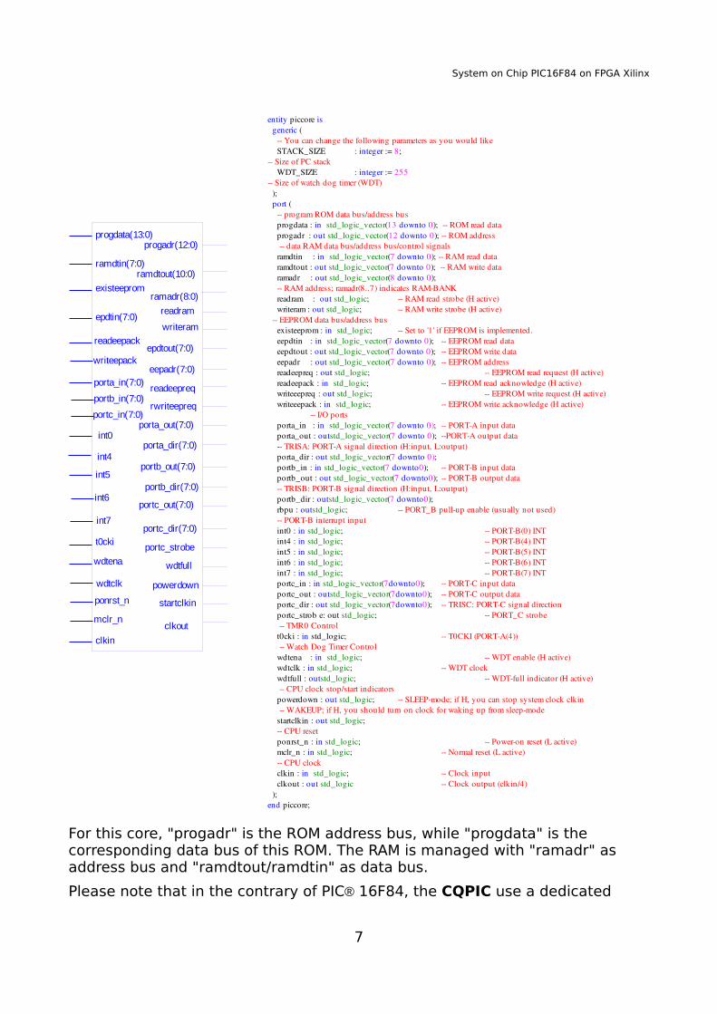
For this core, "progadr" is the ROM address bus, while "progdata" is the corresponding data bus of this ROM. The RAM is managed with "ramadr" as address bus and "ramdtout/ramdtin" as data bus.
Please note that in the contrary of PIC® 16F84, the CQPIC use a dedicated
7
entity piccore is generic ( You can change the following parameters as you would like STACK_SIZE : integer := 8; Size of PC stack WDT_SIZE : integer := 255 Size of watch dog timer (WDT) ); port ( program ROM data bus/address bus progdata : in std_logic_vector(13 downto 0); ROM read data progadr : out std_logic_vector(12 downto 0); ROM address data RAM data bus/address bus/control signals ramdtin : in std_logic_vector(7 downto 0); RAM read data ramdtout : out std_logic_vector(7 downto 0); RAM write data ramadr : out std_logic_vector(8 downto 0); RAM address; ramadr(8..7) indicates RAMBANK readram : out std_logic; RAM read strobe (H active) writeram : out std_logic; RAM write strobe (H active) EEPROM data bus/address bus existeeprom : in std_logic; Set to '1' if EEPROM is implemented. eepdtin : in std_logic_vector(7 downto 0); EEPROM read data eepdtout : out std_logic_vector(7 downto 0); EEPROM write data eepadr : out std_logic_vector(7 downto 0); EEPROM address readeepreq : out std_logic; EEPROM read request (H active) readeepack : in std_logic; EEPROM read acknowledge (H active) writeeepreq : out std_logic; EEPROM write request (H active) writeeepack : in std_logic; EEPROM write acknowledge (H active)
I/O ports porta_in : in std_logic_vector(7 downto 0); PORTA input data porta_out : outstd_logic_vector(7 downto 0); PORTA output data TRISA: PORTA signal direction (H:input, L:output) porta_dir : out std_logic_vector(7 downto 0); portb_in : in std_logic_vector(7 downto0); PORTB input data portb_out : out std_logic_vector(7 downto0); PORTB output data TRISB: PORTB signal direction (H:input, L:output) portb_dir : outstd_logic_vector(7 downto0); rbpu : outstd_logic; PORT_B pullup enable (usually not used) PORTB interrupt input int0 : in std_logic; PORTB(0) INT int4 : in std_logic; PORTB(4) INT int5 : in std_logic; PORTB(5) INT int6 : in std_logic; PORTB(6) INT int7 : in std_logic; PORTB(7) INT portc_in : in std_logic_vector(7downto0); PORTC input data portc_out : outstd_logic_vector(7downto0); PORTC output data portc_dir : out std_logic_vector(7downto0); TRISC: PORTC signal direction portc_strob e: out std_logic; PORT_C strobe TMR0 Control t0cki : in std_logic; T0CKI (PORTA(4)) Watch Dog Timer Control wdtena : in std_logic; WDT enable (H active) wdtclk : in std_logic; WDT clock wdtfull : outstd_logic; WDTfull indicator (H active) CPU clock stop/start indicators powerdown : out std_logic; SLEEPmode; if H, you can stop system clock clkin WAKEUP; if H, you should turn on clock for waking up from sleepmode startclkin : out std_logic; CPU reset ponrst_n : in std_logic; Poweron reset (L active) mclr_n : in std_logic; Normal reset (L active) CPU clock clkin : in std_logic; Clock input clkout : out std_logic Clock output (clkin/4) );end piccore;
progdata(13:0)
ramdtin(7:0)
existeeprom
epdtin(7:0)
porta_in(7:0)
int0
progadr(12:0)
ramdtout(10:0)
ramadr(8:0)
readram
epdtout(7:0)
eepadr(7:0)
readeepreq
writeram
readeepack
rwriteepreq
writeepack
porta_out(7:0)
porta_dir(7:0)
portb_out(7:0)
portb_dir(7:0)
portc_out(7:0)
portc_dir(7:0)
portb_in(7:0)
portc_in(7:0)
int4
int5
int6
int7
portc_strobet0cki
wdtena
wdtclk
wdtfull
powerdown
startclkinponrst_n
mclr_n
clkin
clkout
System on Chip PIC16F84 on FPGA Xilinx
entry TMRCLK for timer0 clock (for PIC® it's the b4 bit T0CKl of PORTA).
Before going further with peripherals we will explore how the I/O ports are working in the next section.
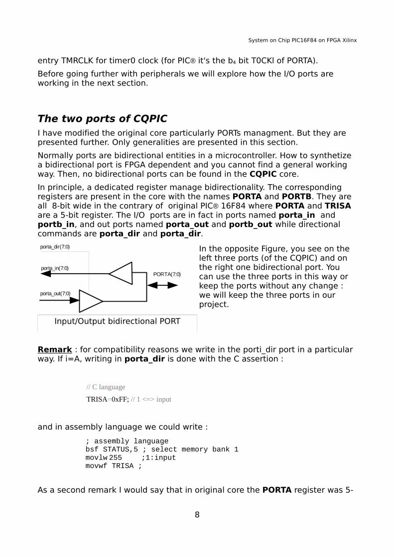
The two ports of CQPICI have modified the original core particularly PORTs managment. But they are presented further. Only generalities are presented in this section.
Normally ports are bidirectional entities in a microcontroller. How to synthetize a bidirectional port is FPGA dependent and you cannot find a general working way. Then, no bidirectional ports can be found in the CQPIC core.
In principle, a dedicated register manage bidirectionality. The corresponding registers are present in the core with the names PORTA and PORTB. They are all 8-bit wide in the contrary of original PIC® 16F84 where PORTA and TRISA are a 5-bit register. The I/O ports are in fact in ports named porta_in and portb_in, and out ports named porta_out and portb_out while directional commands are porta_dir and porta_dir.
In the opposite Figure, you see on the left three ports (of the CQPIC) and on the right one bidirectional port. You can use the three ports in this way or keep the ports without any change : we will keep the three ports in our project.
Input/Output bidirectional PORT
Remark : for compatibility reasons we write in the porti_dir port in a particular way. If i=A, writing in porta_dir is done with the C assertion :
// C language
TRISA=0xFF; // 1 <=> input
and in assembly language we could write :
; assembly languagebsf STATUS,5 ; select memory bank 1 movlw 255 ;1:input movwf TRISA ;
As a second remark I would say that in original core the PORTA register was 5-
8
porta_in(7:0)
porta_out(7:0)
porta_dir(7:0)
PORTA(7:0)
System on Chip PIC16F84 on FPGA Xilinx
bit wide. I have modified the core in CQPIC.VHD file to extend this port as a 8-bit register (see in folder "\CQPICStart\PORTA8"of CQPICStart.zip file).
The last remark is if we write a statement like :
PORTA = PORTA; // une seule diode allumee
in a C program it has the signification : porta_out <= porta_in.
We will come back to the port description when the need of external logic connected with the core will be explained.
RAM and ROM are necessary peripherals to which we now turn.
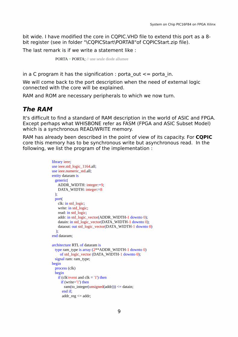
The RAMIt's difficult to find a standard of RAM description in the world of ASIC and FPGA. Except perhaps what WHISBONE refer as FASM (FPGA and ASIC Subset Model) which is a synchronous READ/WRITE memory.
RAM has already been described in the point of view of its capacity. For CQPIC core this memory has to be synchronous write but asynchronous read. In the following, we list the program of the implementation :
library ieee; use ieee.std_logic_1164.all; use ieee.numeric_std.all; entity dataram is generic( ADDR_WIDTH: integer:=9; DATA_WIDTH: integer:=8 ); port( clk: in std_logic; write: in std_logic; read: in std_logic; addr: in std_logic_vector(ADDR_WIDTH-1 downto 0); datain: in std_logic_vector(DATA_WIDTH-1 downto 0); dataout: out std_logic_vector(DATA_WIDTH-1 downto 0) ); end dataram;
architecture RTL of dataram is type ram_type is array (2**ADDR_WIDTH-1 downto 0) of std_logic_vector (DATA_WIDTH-1 downto 0); signal ram: ram_type; begin process (clk) begin if (clk'event and clk = '1') then if (write='1') then ram(to_integer(unsigned(addr))) <= datain; end if; addr_reg <= addr;
9
System on Chip PIC16F84 on FPGA Xilinx
end if; end process;
dataout <= ram(to_integer(unsigned(addr_reg))); end RTL;
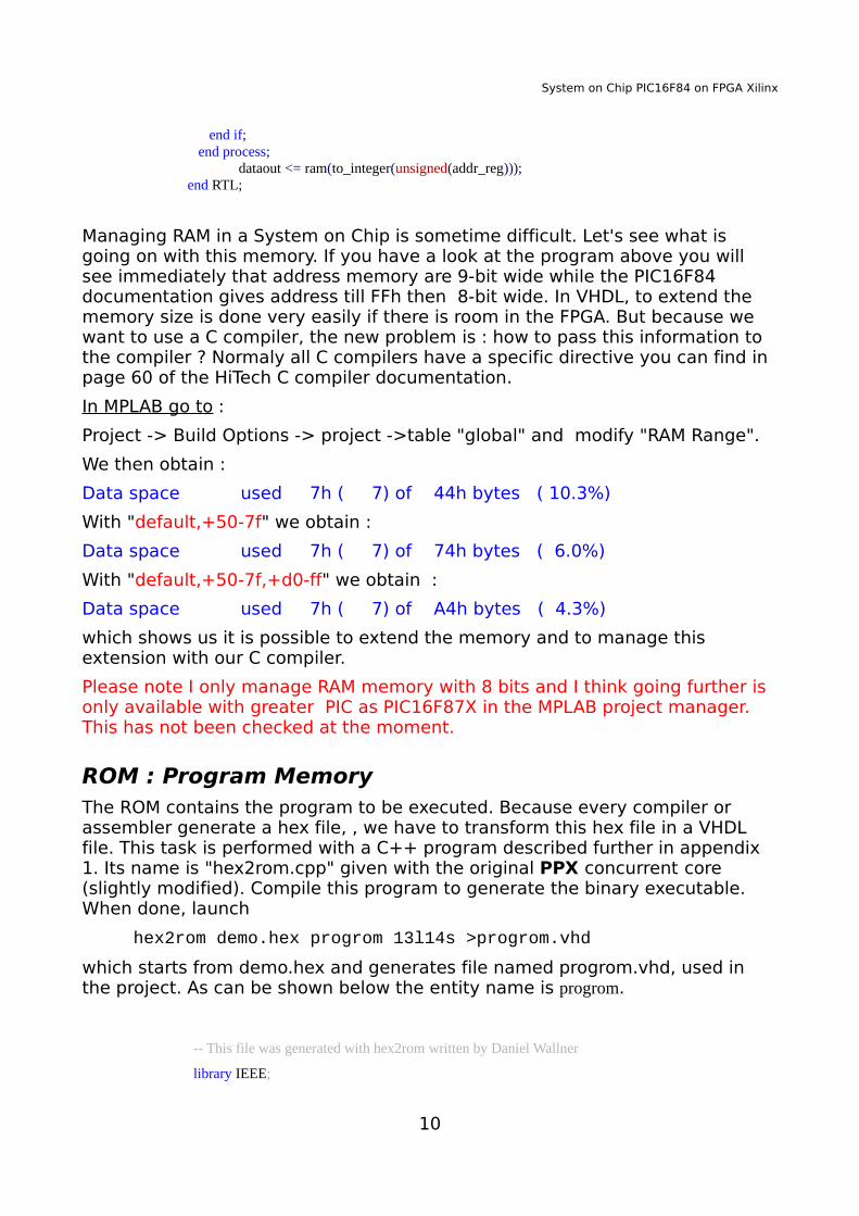
Managing RAM in a System on Chip is sometime difficult. Let's see what is going on with this memory. If you have a look at the program above you will see immediately that address memory are 9-bit wide while the PIC16F84 documentation gives address till FFh then 8-bit wide. In VHDL, to extend the memory size is done very easily if there is room in the FPGA. But because we want to use a C compiler, the new problem is : how to pass this information to the compiler ? Normaly all C compilers have a specific directive you can find in page 60 of the HiTech C compiler documentation.
In MPLAB go to :
Project -> Build Options -> project ->table "global" and modify "RAM Range".
We then obtain :
Data space used 7h ( 7) of 44h bytes ( 10.3%)
With "default,+50-7f" we obtain :
Data space used 7h ( 7) of 74h bytes ( 6.0%)
With "default,+50-7f,+d0-ff" we obtain :
Data space used 7h ( 7) of A4h bytes ( 4.3%)
which shows us it is possible to extend the memory and to manage this extension with our C compiler.
Please note I only manage RAM memory with 8 bits and I think going further is only available with greater PIC as PIC16F87X in the MPLAB project manager. This has not been checked at the moment.
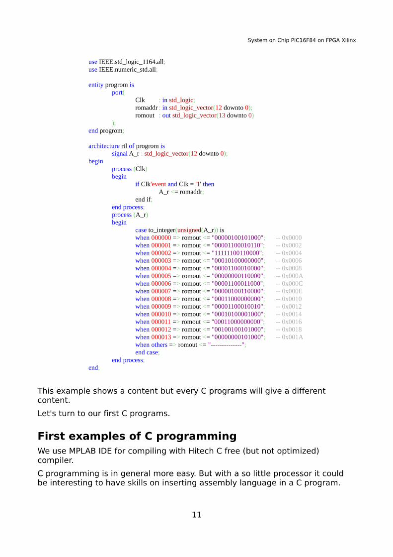
ROM : Program MemoryThe ROM contains the program to be executed. Because every compiler or assembler generate a hex file, , we have to transform this hex file in a VHDL file. This task is performed with a C++ program described further in appendix 1. Its name is "hex2rom.cpp" given with the original PPX concurrent core (slightly modified). Compile this program to generate the binary executable. When done, launch
hex2rom demo.hex progrom 13l14s >progrom.vhd
which starts from demo.hex and generates file named progrom.vhd, used in the project. As can be shown below the entity name is progrom.
-- This file was generated with hex2rom written by Daniel Wallner
library IEEE;
10
System on Chip PIC16F84 on FPGA Xilinx
use IEEE.std_logic_1164.all; use IEEE.numeric_std.all;
entity progrom is port(
Clk : in std_logic; romaddr : in std_logic_vector(12 downto 0); romout : out std_logic_vector(13 downto 0)
); end progrom;
architecture rtl of progrom is signal A_r : std_logic_vector(12 downto 0);
begin process (Clk) begin
if Clk'event and Clk = '1' then A_r <= romaddr;
end if; end process; process (A_r) begin
case to_integer(unsigned(A_r)) is when 000000 => romout <= "00000100101000"; -- 0x0000 when 000001 => romout <= "00001100010110"; -- 0x0002 when 000002 => romout <= "11111100110000"; -- 0x0004 when 000003 => romout <= "00010100000000"; -- 0x0006 when 000004 => romout <= "00001100010000"; -- 0x0008 when 000005 => romout <= "00000000110000"; -- 0x000A when 000006 => romout <= "00001100011000"; -- 0x000C when 000007 => romout <= "00000100110000"; -- 0x000E when 000008 => romout <= "00011000000000"; -- 0x0010 when 000009 => romout <= "00001100010010"; -- 0x0012 when 000010 => romout <= "00010100001000"; -- 0x0014 when 000011 => romout <= "00011000000000"; -- 0x0016 when 000012 => romout <= "00100100101000"; -- 0x0018 when 000013 => romout <= "00000000101000"; -- 0x001A when others => romout <= "--------------"; end case;
end process; end;
This example shows a content but every C programs will give a different content.
Let's turn to our first C programs.
First examples of C programmingWe use MPLAB IDE for compiling with Hitech C free (but not optimized) compiler.
C programming is in general more easy. But with a so little processor it could be interesting to have skills on inserting assembly language in a C program.
11
System on Chip PIC16F84 on FPGA Xilinx
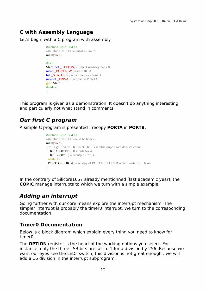
C with Assembly Language
Let's begin with a C program with assembly.
#include <pic1684.h> //#include <htc.h> serait-il mieux ?main(void) { #asm Start: bcf _STATUS,5 ; select memory bank 0 movf _PORTA, W ;read PORTA bsf _STATUS,5 ; select memory bank 1 movwf _TRISA ;Recopie de PORTA goto Start #endasm }
This program is given as a demonstration. It doesn't do anything interesting and particularly not what stand in comments.
Our first C program A simple C program is presented : recopy PORTA in PORTB.
#include <pic1684.h> //#include <htc.h> would be better ?main(void) { // La gestion de TRISA et TRISB semble importante dans ce coeur TRISA = 0xFF; // 8 inputs for A TRISB = 0x00; // 8 outputs for B while(1) PORTB = PORTA; // recopy of PORTA in PORTB which switch LEDs on}
In the contrary of Silicore1657 already mentionned (last academic year), the CQPIC manage interrupts to which we turn with a simple example.
Adding an interruptGoing further with our core means explore the interrupt mechanism. The simpler interrupt is probably the timer0 interrupt. We turn to the corresponding documentation.
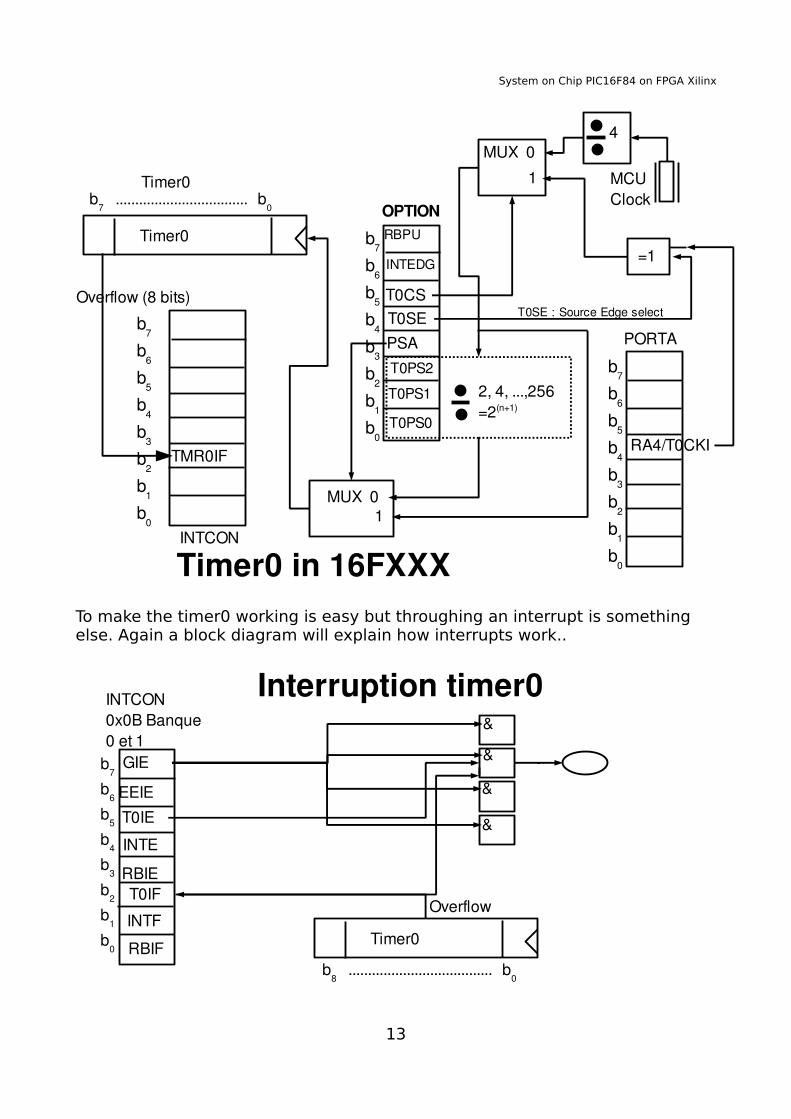
Timer0 Documentation
Below is a block diagram which explain every thing you need to know for timer0.
The OPTION register is the heart of the working options you select. For instance, only the three LSB bits are set to 1 for a division by 256. Because we want our eyes see the LEDs switch, this division is not great enough : we will add a 16 division in the interrupt subprogram.
12
System on Chip PIC16F84 on FPGA Xilinx
To make the timer0 working is easy but throughing an interrupt is something else. Again a block diagram will explain how interrupts work..
13
INTCON
RA4/T0CKI
b7 ..................................
b
0 OPTION
b7
b6
b5
b4
b3
b2
b1
b0
PORTA
b7
b6
b5
b4
b3
b2
b1
b0
Timer0
Timer0 in 16FXXX
T0CS
MCUClock
=1
T0SEPSA
MUX 0
2, 4, ...,256=2(n+1)
MUX 01
1
T0PS2
T0PS1
T0PS0
RBPU
INTEDG
Timer0
4
T0SE : Source Edge selectb
7
b6
b5
b4
b3
b2
b1
b0
TMR0IF
Overflow (8 bits)
b7
b6
b5
b4
b3
b2
b1
b0
T0IE
INTE
RBIET0IF
INTF
RBIF
GIE
EEIE
INTCON0x0B Banque 0 et 1
&
&
&
&
Timer0
Overflow
Interruption timer0
b8 .....................................
b
0
System on Chip PIC16F84 on FPGA Xilinx
To realize the interrupt is done when a rising edge is present in the ellipse : we immediately deduce we have to set 1 in INTCON, exactly in T0IE and GIE.
The Correponding Program
Here is our first program with an interrupt.
#include <pic1684.h> void interrupt decalage(void);
unsigned char nb; main(void) { TRISA = 0xF9; // 6 entrees, 2 sorties pour A TRISB = 0x00; // 8 sorties pour B OPTION = 0x07; // prescaler 256 , entree sur quartz INTCON = 0xA0; // autorise l'interruption timer PORTB = 0x01; // une seule diode allumee TMR0 = 0x00 ; nb=0; while(1) { // on ne fait rien que recopier sur 2 segments la valeur de SW1 if ((PORTA & 0x01) == 1) PORTA = 0x06; } }
void interrupt decalage(void) { nb++; //TMR0 = 0x00; //c'est fait car overflow if (!(nb % 16)) PORTB = (PORTB << 1) ; if (PORTB == 0x00) PORTB = 0x01; T0IF = 0; // acquittement interruption }
Have you seen the "if (!(nb % 16))" which realize a division by 16 in the interrupt. It's because of the 50 MHz clock of our core. Note that a division by 16 is faster done with a mask but such optimization are not important with our project because every C program will spend a lot of time to wait.
Let's turn to VGA hardware.
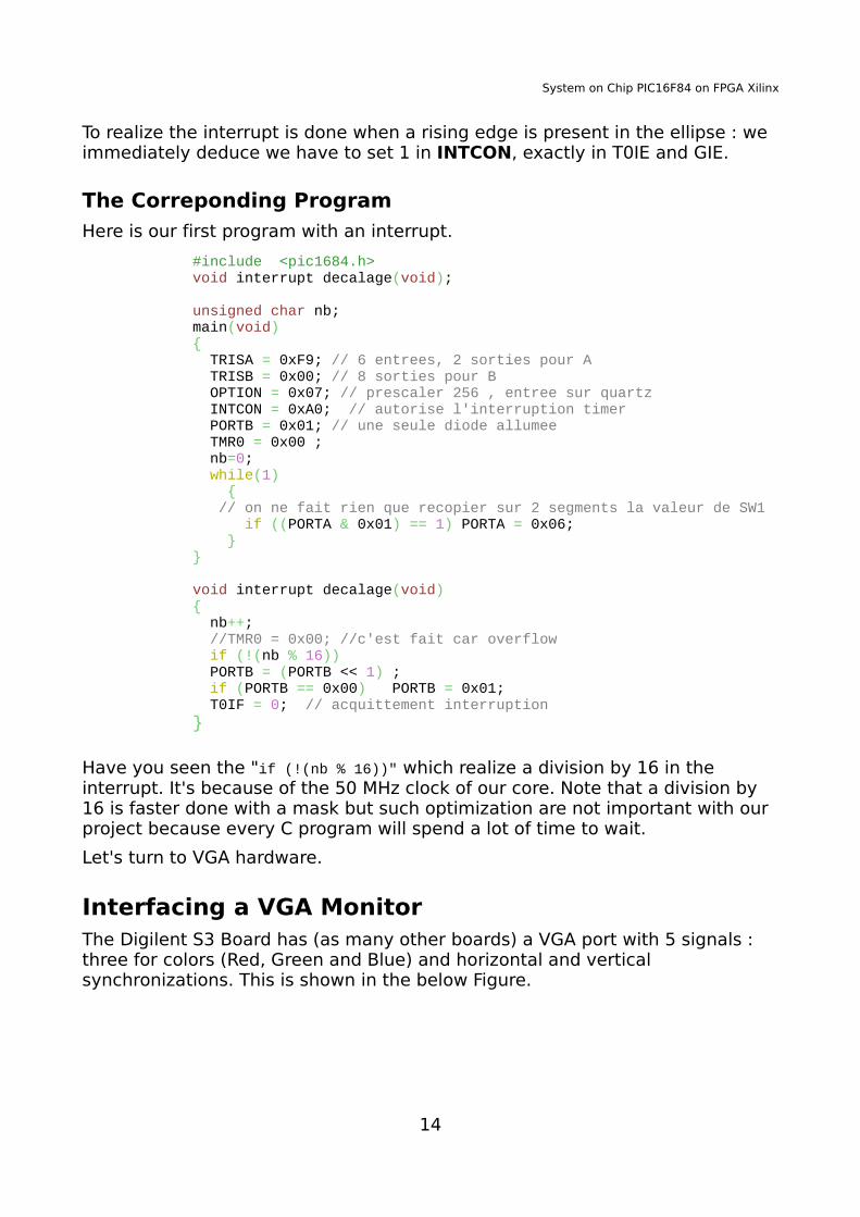
Interfacing a VGA MonitorThe Digilent S3 Board has (as many other boards) a VGA port with 5 signals : three for colors (Red, Green and Blue) and horizontal and vertical synchronizations. This is shown in the below Figure.
14
System on Chip PIC16F84 on FPGA Xilinx
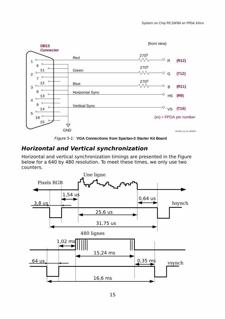
Horizontal and Vertical synchronizationHorizontal and vertical synchronization timings are presented in the Figure below for a 640 by 480 resolution. To meet these times, we only use two counters.
15
Pixels RGB
Une ligne
480 lignes
hsynch
vsynch
31,75 us
25,6 us
0,64 us1,54 us
3,8 us
15,24 ms
64 us
16,6 ms
1,02 ms
0,35 ms
Figure 5-1: VGA Connections from Spartan-3 Starter Kit Board
1 6
112 7
123 8
134 9
145
1015
GND
DB15Connector
Red
Green
Blue
Horizontal Sync
Vertical Sync
270?
270?
270?
R
G
B
HS
VS
(R12)
(T12)
(R11)
(R9)
(T10)
(front view)
(xx) = FPGA pin number
UG130_c5_01_042604
System on Chip PIC16F84 on FPGA Xilinx
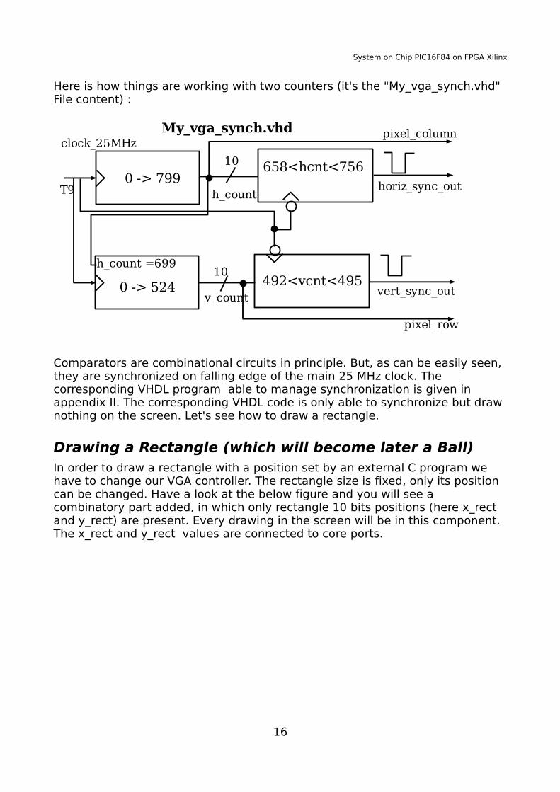
Here is how things are working with two counters (it's the "My_vga_synch.vhd" File content) :
Comparators are combinational circuits in principle. But, as can be easily seen, they are synchronized on falling edge of the main 25 MHz clock. The corresponding VHDL program able to manage synchronization is given in appendix II. The corresponding VHDL code is only able to synchronize but draw nothing on the screen. Let's see how to draw a rectangle.
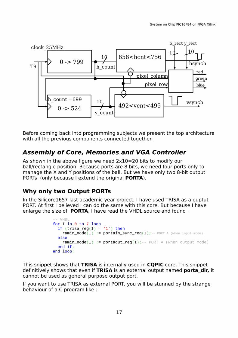
Drawing a Rectangle (which will become later a Ball)In order to draw a rectangle with a position set by an external C program we have to change our VGA controller. The rectangle size is fixed, only its position can be changed. Have a look at the below figure and you will see a combinatory part added, in which only rectangle 10 bits positions (here x_rect and y_rect) are present. Every drawing in the screen will be in this component. The x_rect and y_rect values are connected to core ports.
16
0 -> 799
0 -> 524
658<hcnt<756
492<vcnt<495vert_sync_out
h_count
clock_25MHz
T9
h_count =699
10
10
v_count
horiz_sync_out
pixel_row
pixel_columnMy_vga_synch.vhd
System on Chip PIC16F84 on FPGA Xilinx
Before coming back into programming subjects we present the top architecture with all the previous components connected together.
Assembly of Core, Memories and VGA ControllerAs shown in the above figure we need 2x10=20 bits to modify our ball/rectangle position. Because ports are 8 bits, we need four ports only to manage the X and Y positions of the ball. But we have only two 8-bit output PORTs (only because I extend the original PORTA).
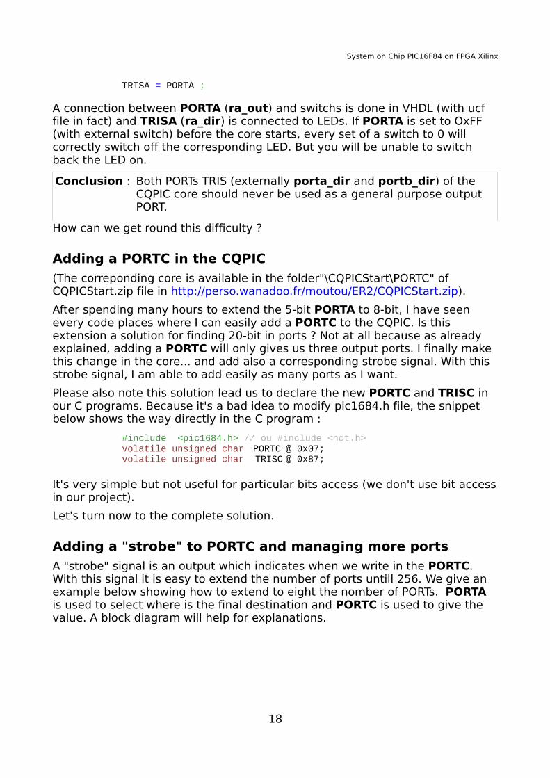
Why only two Output PORTs
In the Silicore1657 last academic year project, I have used TRISA as a ouptut PORT. At first I believed I can do the same with this core. But because I have enlarge the size of PORTA, I have read the VHDL source and found :
-- VHDLfor I in 0 to 7 loop if (trisa_reg(I) = '1') then ramin_node(I) := portain_sync_reg(I);-- PORT A (when input mode) else ramin_node(I) := portaout_reg(I);-- PORT A (when output mode) end if; end loop;
This snippet shows that TRISA is internally used in CQPIC core. This snippet definitively shows that even if TRISA is an external output named porta_dir, it cannot be used as general purpose output port.
If you want to use TRISA as external PORT, you will be stunned by the strange behaviour of a C program like :
17
0 -> 799
0 -> 524
658<hcnt<756
492<vcnt<495vsynch
hsynchT9
red
green
blue
y_rectx_rect
10
10
10 10clock_25MHz
h_count
v_count
h_count =699
pixel_row
pixel_column
System on Chip PIC16F84 on FPGA Xilinx
TRISA = PORTA ;
A connection between PORTA (ra_out) and switchs is done in VHDL (with ucf file in fact) and TRISA (ra_dir) is connected to LEDs. If PORTA is set to OxFF (with external switch) before the core starts, every set of a switch to 0 will correctly switch off the corresponding LED. But you will be unable to switch back the LED on.
Conclusion : Both PORTs TRIS (externally porta_dir and portb_dir) of the CQPIC core should never be used as a general purpose output PORT.
How can we get round this difficulty ?
Adding a PORTC in the CQPIC
(The correponding core is available in the folder"\CQPICStart\PORTC" of CQPICStart.zip file in http://perso.wanadoo.fr/moutou/ER2/CQPICStart.zip).
After spending many hours to extend the 5-bit PORTA to 8-bit, I have seen every code places where I can easily add a PORTC to the CQPIC. Is this extension a solution for finding 20-bit in ports ? Not at all because as already explained, adding a PORTC will only gives us three output ports. I finally make this change in the core... and add also a corresponding strobe signal. With this strobe signal, I am able to add easily as many ports as I want.
Please also note this solution lead us to declare the new PORTC and TRISC in our C programs. Because it's a bad idea to modify pic1684.h file, the snippet below shows the way directly in the C program :
#include <pic1684.h> // ou #include <hct.h>volatile unsigned char PORTC @ 0x07; volatile unsigned char TRISC @ 0x87;
It's very simple but not useful for particular bits access (we don't use bit access in our project).
Let's turn now to the complete solution.
Adding a "strobe" to PORTC and managing more ports
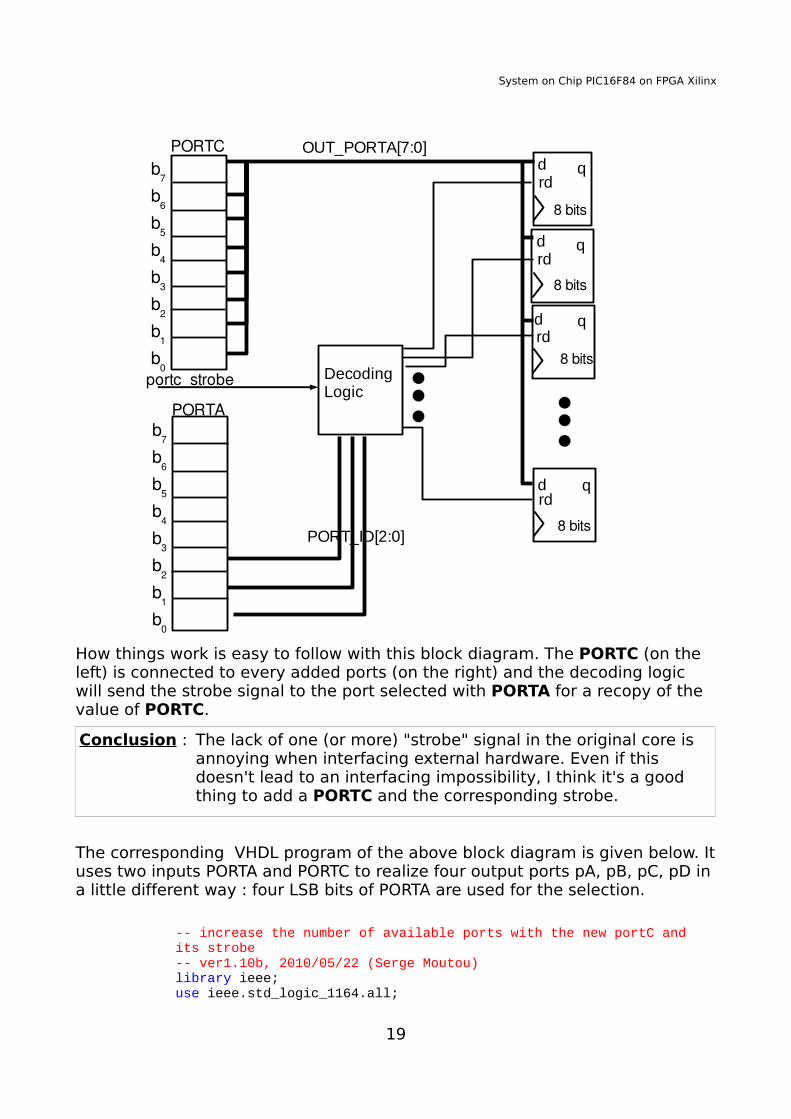
A "strobe" signal is an output which indicates when we write in the PORTC. With this signal it is easy to extend the number of ports untill 256. We give an example below showing how to extend to eight the nomber of PORTs. PORTA is used to select where is the final destination and PORTC is used to give the value. A block diagram will help for explanations.
18
System on Chip PIC16F84 on FPGA Xilinx
How things work is easy to follow with this block diagram. The PORTC (on the left) is connected to every added ports (on the right) and the decoding logic will send the strobe signal to the port selected with PORTA for a recopy of the value of PORTC.
Conclusion : The lack of one (or more) "strobe" signal in the original core is annoying when interfacing external hardware. Even if this doesn't lead to an interfacing impossibility, I think it's a good thing to add a PORTC and the corresponding strobe.
The corresponding VHDL program of the above block diagram is given below. It uses two inputs PORTA and PORTC to realize four output ports pA, pB, pC, pD in a little different way : four LSB bits of PORTA are used for the selection.
-- increase the number of available ports with the new portC and its strobe -- ver1.10b, 2010/05/22 (Serge Moutou) library ieee; use ieee.std_logic_1164.all;
19
b7
b6
b5
b4
b3
b2
b1
b0
PORTC
portc_strobe
8 bits
b7
b6
b5
b4
b3
b2
b1
b0
PORTA
OUT_PORTA[7:0]
PORT_ID[2:0]
rd
rd
rd
Decoding Logic
d
d
d
q
q
q
rdd q
8 bits
8 bits
8 bits
System on Chip PIC16F84 on FPGA Xilinx
entity ports is port( clk : in std_logic; strobeC_in : in std_logic; portA : in std_logic_vector(7 downto 0); portC : in std_logic_vector(7 downto 0); pA,pB,pC,pD : out std_logic_vector(7 downto 0) --new ports );
end ports; architecture BehPorts of ports is signal Internal_strobes : std_logic_vector(7 downto 0);
begin dmux_Strobe:process(portA,strobeC_in) begin case portA is
when "00000001" => Internal_strobes(0) <= strobeC_in; when "00000010" => Internal_strobes(1) <= strobeC_in; when "00000100" => Internal_strobes(2) <= strobeC_in;
when "00001000" => Internal_strobes(3) <= strobeC_in; when others => internal_strobes <= (others =>'0'); end case;
end process; port_A:process(clk)begin if clk'event and clk='1' then
if Internal_strobes="00000001" then pA<=portC; end if;
end if; end process; port_B:process(clk)begin if clk'event and clk='1' then if Internal_strobes="00000010" then
pB<=portC; end if;
end if; end process; port_C:process(clk)begin if clk'event and clk='1' then if Internal_strobes="00000100" then
pC<=portC; end if;
end if; end process; port_D:process(clk)begin if clk'event and clk='1' then if Internal_strobes="00001000" then
pD<=portC; end if;
end if; end process; end BehPorts;
Programming our core with VGA monitor(Have a look at the "\CQPICStart\VGA_Pong"folder of CQPICStart.zip file).
The four ports are connected with the 20-bit inputs of the VGA hardware. This
20
System on Chip PIC16F84 on FPGA Xilinx
means it's now possible to move a rectangle a ball with a program.
C ProgrammingLet's begin with a subprogram which write a 16-bit value in two new PORTs.
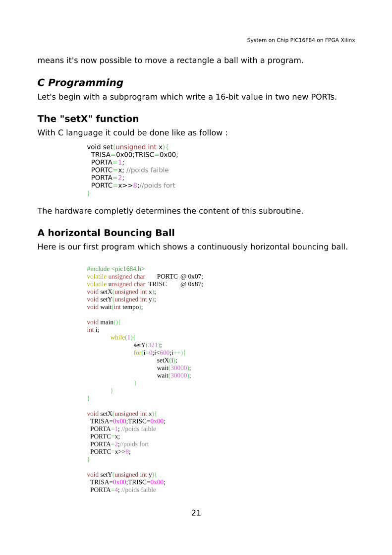
The "setX" function
With C language it could be done like as follow :
void set(unsigned int x){ TRISA=0x00;TRISC=0x00; PORTA=1; PORTC=x; //poids faible PORTA=2; PORTC=x>>8;//poids fort }
The hardware completly determines the content of this subroutine.
A horizontal Bouncing Ball
Here is our first program which shows a continuously horizontal bouncing ball.
#include <pic1684.h>volatile unsigned char PORTC @ 0x07; volatile unsigned char TRISC @ 0x87; void setX(unsigned int x); void setY(unsigned int y); void wait(int tempo);
void main(){ int i;
while(1){ setY(321); for(i=0;i<600;i++){
setX(i); wait(30000); wait(30000);
} }
}
void setX(unsigned int x){ TRISA=0x00;TRISC=0x00; PORTA=1; //poids faible PORTC=x; PORTA=2;//poids fort PORTC=x>>8;}
void setY(unsigned int y){ TRISA=0x00;TRISC=0x00; PORTA=4; //poids faible
21
System on Chip PIC16F84 on FPGA Xilinx
PORTC=x; PORTA=8;//poids fort PORTC=x>>8;}
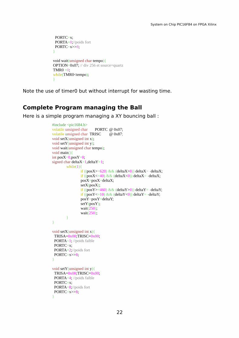
void wait(unsigned char tempo){ OPTION=0x07; // div 256 et source=quartz TMR0 =0; while(TMR0<tempo); }
Note the use of timer0 but without interrupt for wasting time.
Complete Program managing the Ball
Here is a simple program managing a XY bouncing ball :
#include <pic1684.h> volatile unsigned char PORTC @ 0x07; volatile unsigned char TRISC @ 0x87; void setX(unsigned int x); void setY(unsigned int y); void wait(unsigned char tempo); void main(){ int posX=0,posY=0; signed char deltaX=1,deltaY=1;
while(1){ if ((posX>=620) && (deltaX>0)) deltaX= -deltaX; if ((posX<=40) && (deltaX<0)) deltaX= -deltaX; posX=posX+deltaX; setX(posX); if ((posY>=460) && (deltaY>0)) deltaY= -deltaY; if ((posY<=10) && (deltaY<0)) deltaY= -deltaY; posY=posY+deltaY; setY(posY); wait(250); wait(250);
} }
void setX(unsigned int x){ TRISA=0x00;TRISC=0x00; PORTA=1; //poids faible PORTC=x; PORTA=2;//poids fort PORTC=x>>8;}
void setY(unsigned int y){ TRISA=0x00;TRISC=0x00; PORTA=4; //poids faible PORTC=x; PORTA=8;//poids fort PORTC=x>>8;}
22
System on Chip PIC16F84 on FPGA Xilinx
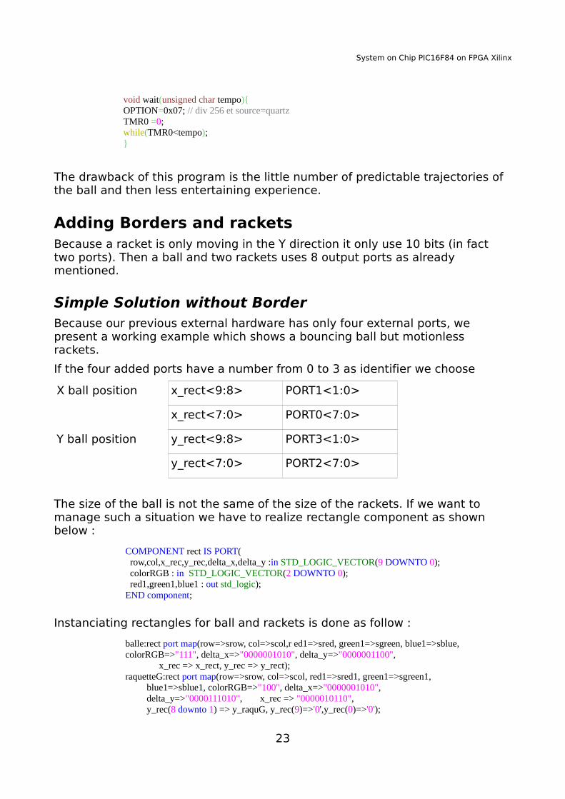
void wait(unsigned char tempo){ OPTION=0x07; // div 256 et source=quartz TMR0 =0; while(TMR0<tempo); }
The drawback of this program is the little number of predictable trajectories of the ball and then less entertaining experience.
Adding Borders and racketsBecause a racket is only moving in the Y direction it only use 10 bits (in fact two ports). Then a ball and two rackets uses 8 output ports as already mentioned.
Simple Solution without BorderBecause our previous external hardware has only four external ports, we present a working example which shows a bouncing ball but motionless rackets.
If the four added ports have a number from 0 to 3 as identifier we choose
X ball position x_rect<9:8> PORT1<1:0>
x_rect<7:0> PORT0<7:0>
Y ball position y_rect<9:8> PORT3<1:0>
y_rect<7:0> PORT2<7:0>
The size of the ball is not the same of the size of the rackets. If we want to manage such a situation we have to realize rectangle component as shown below :
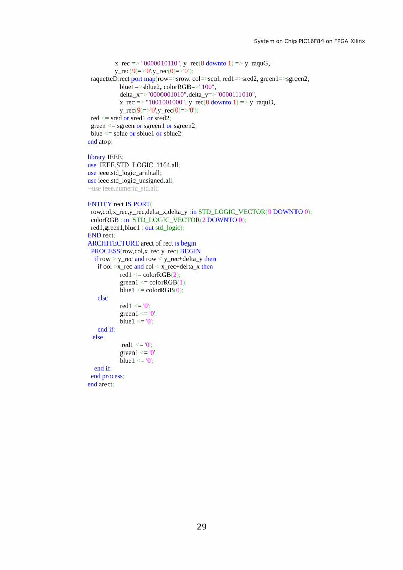
COMPONENT rect IS PORT( row,col,x_rec,y_rec,delta_x,delta_y :in STD_LOGIC_VECTOR(9 DOWNTO 0); colorRGB : in STD_LOGIC_VECTOR(2 DOWNTO 0); red1,green1,blue1 : out std_logic); END component;
Instanciating rectangles for ball and rackets is done as follow :
balle:rect port map(row=>srow, col=>scol,r ed1=>sred, green1=>sgreen, blue1=>sblue, colorRGB=>"111", delta_x=>"0000001010", delta_y=>"0000001100",
x_rec => x_rect, y_rec => y_rect); raquetteG:rect port map(row=>srow, col=>scol, red1=>sred1, green1=>sgreen1, blue1=>sblue1, colorRGB=>"100", delta_x=>"0000001010", delta_y=>"0000111010", x_rec => "0000010110", y_rec(8 downto 1) => y_raquG, y_rec(9)=>'0',y_rec(0)=>'0');
23
System on Chip PIC16F84 on FPGA Xilinx
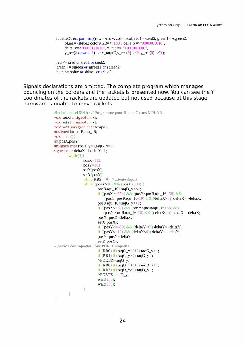
raquetteD:rect port map(row=>srow, col=>scol, red1=>sred2, green1=>sgreen2, blue1=>sblue2,colorRGB=>"100", delta_x=>"0000001010", delta_y=>"0000111010", x_rec => "1001001000", y_rec(8 downto 1) => y_raquD,y_rec(9)=>'0',y_rec(0)=>'0');
red <= sred or sred1 or sred2; green <= sgreen or sgreen1 or sgreen2; blue <= sblue or sblue1 or sblue2;
Signals declarations are omitted. The complete program which manages bouncing on the borders and the rackets is presented now. You can see the Y coordinates of the rackets are updated but not used because at this stage hardware is unable to move rackets.
#include <pic1684.h> // Programme pour Hitech C dans MPLABvoid setX(unsigned int x); void setY(unsigned int y); void wait(unsigned char tempo); unsigned int posRaqu_16; void main(){ int posX,posY; unsigned char raqD_y=0,raqG_y=0; signed char deltaX=1,deltaY=1;
while(1){ posX=113; posY=101; setX(posX); setY(posY); while(RB2==0); // attente départ while( (posX>30) && (posX<580)){
posRaqu_16=raqD_y<<1; if ((posX>=574) && (posY<posRaqu_16+58) &&
(posY>posRaqu_16-10) && (deltaX>0)) deltaX= -deltaX; posRaqu_16=raqG_y<<1; if ((posX<=32) && (posY<posRaqu_16+58) &&
(posY>posRaqu_16-10) && (deltaX<0)) deltaX= -deltaX; posX=posX+deltaX; setX(posX); if ((posY>=460) && (deltaY>0)) deltaY= -deltaY; if ((posY<=10) && (deltaY<0)) deltaY= -deltaY; posY=posY+deltaY; setY(posY);
// gestion des raquettes 2bits PORTC/raquette if (RB0) if (raqG_y<215) raqG_y++;
if (RB1) if (raqG_y>0) raqG_y--; //PORTD=raqG_y;
if (RB6) if (raqD_y<215) raqD_y++; if (RB7) if (raqD_y>0) raqD_y--; //PORTE=raqD_y; wait(250); wait(250);
} }
}
24
System on Chip PIC16F84 on FPGA Xilinx
As can be easily seen, we choose sw0,sw1,sw6 and sw7 switchs of the board connected to input PORTB to move up and down the rackets and sw2 (RC2) for the start.
What your Work consists of ?
The complete understanding of hardware (project preparation)You have to be able to draw all the components and their connections starting from the given VHDL files ("\CQPICStart\VGA_Pong" folder of CQPICStart.zip file).
Extend the Hardware (project preparation)You have to extend the harware and then manage the rackets positions. You can choose to manage both the Y coordinates of each racket with one 8-bit port (leading then the hardware with 6 ports) or with 10-bit (leading then the hardware with 8 ports)
Developping in C languageDesign a C program for managing rackets move with first the switchs and second the joysticks.
Bresenham Line Algorithm
Explore if it is possible to use Bresenham's line algorithm for trajectories and so enlarge considerably the number of them. This algorithm is explain in WIKI : http://en.wikipedia.org/wiki/Bresenham's_line_algorithm
You can directly find a C version in the Internet : google Bresenham in C.
Managing Scores
Use the bottom of the VGA monitor to print scores in character mode.Every time a ball is lost a new score is printed.
AcknowledgementsThanks to Xilinx University Program for giving us gracefully five Digilent S3 Starter Board used in our students projects and practices.
Written with OpenOffice 2.4.1 under Linux
25
System on Chip PIC16F84 on FPGA Xilinx
APPENDIX I (transforming a HEX into VHDL)
The complete C++ program to transform the hex file into a VHDL file is not given here because its size. You can find it in "\CQPICStart\ROM" folder of "http://perso.wanadoo.fr/moutou/ER2/CQPICStart.zip" file.
Attention : I have not used the original hex2vhd.c file we can find in CQPIC core because it never works correctly. I have taken the C++ hex2rom.cpp file you can find in the concurent PPX project. This file is slightly modified to fit directly in our VHDL project.
When compiled the binary executable is named hex2rom.exe (under Windows) or hex2rom under Linux.
Use the command line :
hex2rom demo16F84.hex progrom 13l14s >progrom.vhd
if the starting file is demo16F84.hex.
The destination file is progrom.vhd with "progrom" as entity.
13 means 13-bit address,
l means little indian convention (b would be big indian)
14 means 14-bit data ROM.
26
System on Chip PIC16F84 on FPGA Xilinx
Appendix II VHDL module to manage VGAHere is a complete VHDL module to manage completly VGA synchronization with a ball and two rackets (see "\CQPICStart\VGA_Pong" folder of CQPICStart.zip file).
-- ************* My_vga_synch.vhd ***********library IEEE; use IEEE.STD_LOGIC_1164.all; use IEEE.STD_LOGIC_ARITH.all; use IEEE.STD_LOGIC_UNSIGNED.all;
ENTITY VGA_SYNC IS PORT( clock_25Mhz : IN STD_LOGIC; horiz_sync_out, vert_sync_out : OUT STD_LOGIC; pixel_row, pixel_column: OUT STD_LOGIC_VECTOR(9 DOWNTO 0));
END VGA_SYNC; ARCHITECTURE a OF VGA_SYNC IS
SIGNAL horiz_sync, vert_sync : STD_LOGIC; SIGNAL h_count, v_count :STD_LOGIC_VECTOR(9 DOWNTO 0);
BEGIN --Generate Horizontal and Vertical Timing Signals for Video Signal -- H_count counts pixels (640 + extra time for sync signals) -- -- Horiz_sync ------------------------------------__________-------- -- H_count 0 640 659 755 799 -- gestion_H_Count:PROCESS(clock_25Mhz) BEGIN
IF(clock_25Mhz'EVENT) AND (clock_25Mhz='1') THEN IF (h_count = 799) THEN
h_count <= (others =>'0'); ELSE
h_count <= h_count + 1; END IF;
END IF; END PROCESS; gestion_Horiz_sync: PROCESS(clock_25Mhz,h_count) BEGIN --Generate Horizontal Sync Signal using H_count IF(clock_25Mhz'EVENT) AND (clock_25Mhz='0') THEN
IF (h_count <= 755) AND (h_count >= 659) THEN horiz_sync <= '0';
ELSE horiz_sync <= '1';
END IF; END IF; END PROCESS; --V_count counts rows of pixels (480 + extra time for sync signals) -- -- Vert_sync -----------------------------------------------_______------------ -- V_count 0 480 493-494 524 -- gestion_V_Count: PROCESS(clock_25Mhz,h_count) BEGIN
IF(clock_25Mhz'EVENT) AND (clock_25Mhz='1') THEN IF (v_count >= 524) AND (h_count >= 699) THEN
v_count <= (others =>'0'); ELSIF (h_count = 699) THEN
27
System on Chip PIC16F84 on FPGA Xilinx
v_count <= v_count + 1; END IF; END IF;
END PROCESS; gestion_Vertical_sync:PROCESS(clock_25Mhz,v_count) BEGIN
IF(clock_25Mhz'EVENT) AND (clock_25Mhz='0') THEN -- Generate Vertical Sync Signal using V_count
IF (v_count <= 494) AND (v_count >= 493) THEN vert_sync <= '0';
ELSE vert_sync <= '1';
END IF; END IF;
END PROCESS; pixel_column <= h_count; pixel_row <= v_count; horiz_sync_out <= horiz_sync; vert_sync_out <= vert_sync; END a;
library IEEE; use IEEE.STD_LOGIC_1164.all; ENTITY VGAtop IS PORT (clk_50 : in STD_LOGIC;
x_rect, y_rect: IN STD_LOGIC_VECTOR(9 DOWNTO 0); y_raquG, y_raquD: IN STD_LOGIC_VECTOR(7 DOWNTO 0);
hsynch,vsynch,red,green,blue : out STD_LOGIC); END VGAtop; ARCHITECTURE atop of VGAtop is COMPONENT VGA_SYNC IS
PORT( clock_25Mhz : IN STD_LOGIC; horiz_sync_out, vert_sync_out : OUT STD_LOGIC; pixel_row, pixel_column: OUT STD_LOGIC_VECTOR(9 DOWNTO 0));
END COMPONENT; COMPONENT rect IS PORT( row,col,x_rec,y_rec,delta_x,delta_y :in STD_LOGIC_VECTOR(9 DOWNTO 0); colorRGB : in STD_LOGIC_VECTOR(2 DOWNTO 0); red1,green1,blue1 : out std_logic); END component; signal clk_25,sred,sgreen,sblue,sred1,sgreen1,sblue1,sred2,sgreen2,sblue2 : std_logic; signal srow,scol : STD_LOGIC_VECTOR(9 DOWNTO 0); begin process(clk_50) begin if clk_50'event and clk_50='1' then
clk_25 <= not clk_25; end if;
end process; i1:vga_sync port map(clock_25Mhz =>clk_25, horiz_sync_out=>hsynch, vert_sync_out=>vsynch, pixel_row=>srow, pixel_column=>scol); balle:rect port map(row=>srow, col=>scol, red1=>sred, green1=>sgreen, blue1=>sblue,colorRGB=>"111", delta_x=>"0000001010",delta_y=>"0000001100",
x_rec => x_rect, y_rec => y_rect); raquetteG:rect port map(row=>srow, col=>scol, red1=>sred1, green1=>sgreen1, blue1=>sblue1,colorRGB=>"100", delta_x=>"0000001010",delta_y=>"0000111010",
28
System on Chip PIC16F84 on FPGA Xilinx
x_rec => "0000010110", y_rec(8 downto 1) => y_raquG, y_rec(9)=>'0',y_rec(0)=>'0'); raquetteD:rect port map(row=>srow, col=>scol, red1=>sred2, green1=>sgreen2, blue1=>sblue2, colorRGB=>"100", delta_x=>"0000001010",delta_y=>"0000111010", x_rec => "1001001000", y_rec(8 downto 1) => y_raquD, y_rec(9)=>'0',y_rec(0)=>'0'); red <= sred or sred1 or sred2; green <= sgreen or sgreen1 or sgreen2; blue <= sblue or sblue1 or sblue2; end atop;
library IEEE; use IEEE.STD_LOGIC_1164.all; use ieee.std_logic_arith.all; use ieee.std_logic_unsigned.all; --use ieee.numeric_std.all;
ENTITY rect IS PORT( row,col,x_rec,y_rec,delta_x,delta_y :in STD_LOGIC_VECTOR(9 DOWNTO 0); colorRGB : in STD_LOGIC_VECTOR(2 DOWNTO 0); red1,green1,blue1 : out std_logic); END rect; ARCHITECTURE arect of rect is begin PROCESS(row,col,x_rec,y_rec) BEGIN if row > y_rec and row < y_rec+delta_y then if col >x_rec and col < x_rec+delta_x then
red1 <= colorRGB(2); green1 <= colorRGB(1); blue1 <= colorRGB(0);
else red1 <= '0'; green1 <= '0'; blue1 <= '0';
end if; else
red1 <= '0'; green1 <= '0'; blue1 <= '0';
end if; end process; end arect;
29
System on Chip PIC16F84 on FPGA Xilinx
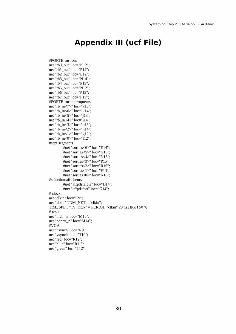
Appendix III (ucf File)
#PORTB sur ledsnet "rb0_out" loc="K12";net "rb1_out" loc="P14";net "rb2_out" loc="L12";net "rb3_out" loc="N14";net "rb4_out" loc="P13";net "rb5_out" loc="N12";net "rb6_out" loc="P12";net "rb7_out" loc="P11";#PORTB sur interrupteursnet "rb_in<7>" loc="k13"; net "rb_in<6>" loc="k14"; net "rb_in<5>" loc="j13"; net "rb_in<4>" loc="j14"; net "rb_in<3>" loc="h13"; net "rb_in<2>" loc="h14"; net "rb_in<1>" loc="g12"; net "rb_in<0>" loc="f12";#sept segments
#net "sorties<6>" loc="E14";#net "sorties<5>" loc="G13";#net "sorties<4>" loc="N15";#net "sorties<3>" loc="P15";#net "sorties<2>" loc="R16";#net "sorties<1>" loc="F13";#net "sorties<0>" loc="N16";
#selection afficheurs#net "affpdsfaible" loc="D14";#net "affpdsfort" loc="G14";
# clocknet "clkin" loc="T9";net "clkin" TNM_NET = "clkin";TIMESPEC "TS_mclk" = PERIOD "clkin" 20 ns HIGH 50 %;# resetnet "mclr_n" loc="M13"; net "ponrst_n" loc="M14";#VGAnet "hsynch" loc="R9";net "vsynch" loc="T10";net "red" loc="R12";net "blue" loc="R11";net "green" loc="T12";
30
System on Chip PIC16F84 on FPGA Xilinx
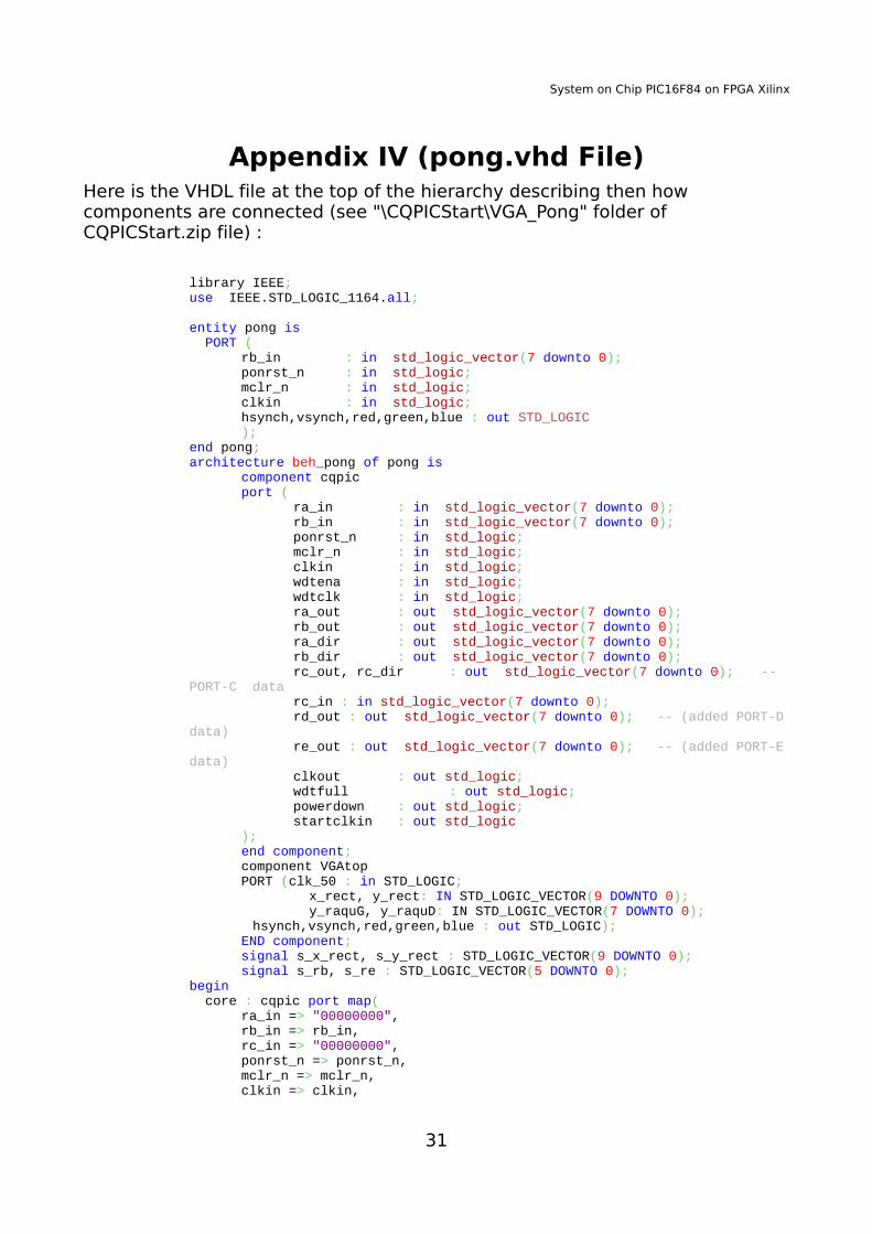
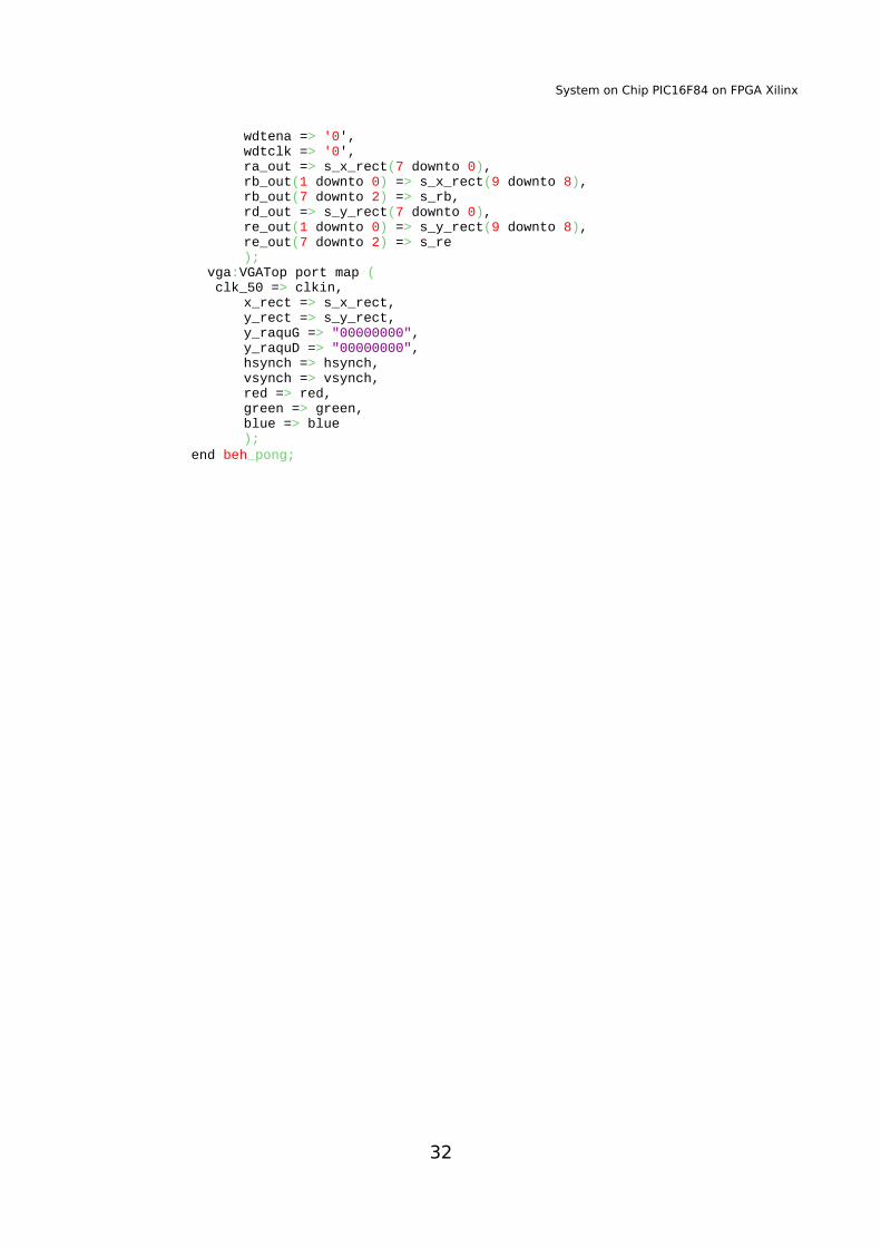
Appendix IV (pong.vhd File)Here is the VHDL file at the top of the hierarchy describing then how components are connected (see "\CQPICStart\VGA_Pong" folder of CQPICStart.zip file) :
library IEEE; use IEEE.STD_LOGIC_1164.all;
entity pong is PORT (
rb_in : in std_logic_vector(7 downto 0); ponrst_n : in std_logic; mclr_n : in std_logic; clkin : in std_logic; hsynch,vsynch,red,green,blue : out STD_LOGIC );
end pong; architecture beh_pong of pong is
component cqpic port (
ra_in : in std_logic_vector(7 downto 0); rb_in : in std_logic_vector(7 downto 0); ponrst_n : in std_logic; mclr_n : in std_logic; clkin : in std_logic; wdtena : in std_logic; wdtclk : in std_logic; ra_out : out std_logic_vector(7 downto 0); rb_out : out std_logic_vector(7 downto 0); ra_dir : out std_logic_vector(7 downto 0); rb_dir : out std_logic_vector(7 downto 0); rc_out, rc_dir : out std_logic_vector(7 downto 0); --
PORT-C data rc_in : in std_logic_vector(7 downto 0); rd_out : out std_logic_vector(7 downto 0); -- (added PORT-D
data) re_out : out std_logic_vector(7 downto 0); -- (added PORT-E
data) clkout : out std_logic; wdtfull : out std_logic; powerdown : out std_logic; startclkin : out std_logic
); end component; component VGAtop PORT (clk_50 : in STD_LOGIC;
x_rect, y_rect: IN STD_LOGIC_VECTOR(9 DOWNTO 0); y_raquG, y_raquD: IN STD_LOGIC_VECTOR(7 DOWNTO 0);
hsynch,vsynch,red,green,blue : out STD_LOGIC); END component; signal s_x_rect, s_y_rect : STD_LOGIC_VECTOR(9 DOWNTO 0); signal s_rb, s_re : STD_LOGIC_VECTOR(5 DOWNTO 0);
begin core : cqpic port map(
ra_in => "00000000", rb_in => rb_in, rc_in => "00000000", ponrst_n => ponrst_n, mclr_n => mclr_n, clkin => clkin,
31
System on Chip PIC16F84 on FPGA Xilinx
wdtena => '0', wdtclk => '0', ra_out => s_x_rect(7 downto 0), rb_out(1 downto 0) => s_x_rect(9 downto 8), rb_out(7 downto 2) => s_rb, rd_out => s_y_rect(7 downto 0), re_out(1 downto 0) => s_y_rect(9 downto 8), re_out(7 downto 2) => s_re );
vga:VGATop port map ( clk_50 => clkin,
x_rect => s_x_rect, y_rect => s_y_rect, y_raquG => "00000000", y_raquD => "00000000", hsynch => hsynch, vsynch => vsynch, red => red, green => green, blue => blue );
end beh_pong;
32


