Embed Size (px)
Citation preview

International Review of Electrical Engineering (I.R.E.E.), Vol. 9, N. 4 ISSN 1827- 6660 July – August 2014
Copyright © 2014 Praise Worthy Prize S.r.l. - All rights reserved
671
Matlab/Simulink Modeling of SiC Power MOSFETs
Paolo Giammatteo, Concettina Buccella, Carlo Cecati Abstract – Simulation and rapid prototyping of power converters requires accurate models of all passive and active elements, which take into account most important physical parameters and not only electrical quantities. Their availability is fundamental to verify the expected behaviour of the complete system including its control algorithm without building any prototype. For this reason, due to the wide use of Simulink® in simulation of complex systems, this paper attempts to study the main characteristics of a typical Silicon Carbide (SiC) power MOSFETs and proposes its Simulink® model. The static and dynamic characteristics of the device are described by voltage and current sources which behaviour depend on temperature values. Switching power losses are considered by introducing parasitic capacitances in its equivalent circuit, thus obtaining a dynamic characteristic of the device. The proposed model has been validated using a typical 4H-SiC MOSFET (1200V, 20A) in an illustrative example consisting of a 5-level cascaded inverter. Copyright © 2014 Praise Worthy Prize S.r.l. - All rights reserved. Keywords: Silicon Carbide, Device Characterization, Device Modeling, Device Simulation,
MOSFET, Loss, Power Converter
Nomenclature α The slope of the temperature variation of the
gate threshold voltage [V°/C ] χSiC Electron affinity of the SiC [J/mol] λ Channel modulation [V-1] μ Electron mobility of SiC [m2V/s] μit Interface traps mobility [m2V/s] μph Phonon scattering mobility [m2V/s] Cb Bulk majority carrier concentration[m-3] Cdg Parasitic gate to drain capacitance [F] Cgs Parasitic gate to source capacitance [F] Ciss Parasitic input capacitance [F] Cox Oxide capacitance [F] Crss Reverse Transfer Capacitance [F] Eeff The average transverse electric field in the
MOSFET channel [V/m] Eg Band gap [J/C] Idstd Drain current at standard temperature[A] Id Drain current [A] Iload Full load darin-source current [A] K Transistor gain [A/V2] KB Boltzman constant [J/°C] L Channel length [m] ni Intrinsic carrier concentrations [m-3] q Carrier charge [C] Qb Bulk charge [C] Qf Fixed oxide charge [C] Qit Interface traps charge [C] Rg Gate resistance [Ω] T Device Temperature [°C] t Time [s] t0 Time at which the gate signal rises up[s] td Time at which the gate signal drops down [s]
Tstd Device standard temperature [°C] Vds,load Full load drain-source voltage [V] Vds,off Device off drain-source voltage [V] Vds Drain-source voltage [V] Vgs Gate-source voltage [V] Vpm Miller plateau voltage [V] Vth Threshold voltage [V] W Channel width [m]
I. Introduction High power converters are widely used many fields
including industry, transportation, oil&gas, lighting, home appliances, moreover, they are fundamental in full exploitation of distributed energy resources (DERs) and in their integration with the grid; they are also very important in ensuring high power factor and fulfilling power quality grid stability demands [1], [2], [3].
Modern systems have to be capable of handling active and reactive power demands, often to operate at high frequency and always to maintain both switching and conduction losses at lowest possible values. Fulfillment of previous requirements impose improvements in all parts including output power devices.
The emerging Silicon Carbide (SiC) and Gallium Nitrite (GaN) technologies [4], are attracting wide attention due to their new level of performance, in particular their ability to operate at high temperature, frequency and voltage [5], [6].
A synopsis of recent complementary technological developments in passives, integrated driver and protection circuitry and electronic packaging are described in [7]. Paper [8] presents the development and

Paolo Giammatteo, Concettina Buccella, Carlo Cecati
Copyright © 2014 Praise Worthy Prize S.r.l. - All rights reserved International Review of Electrical Engineering, Vol. 9, N. 4
672
experimental performance of a three-phase ac–dc–ac converter composed by SiC MOSFET, working at 250 °C junction temperature.The electromagnetic interference filter, thermal system, high temperature package, and gate drive design are discussed in detail.
Currently, SiC devices are considered excellent for power electronic applications in virtue of their extremely robust and stable behavior even at high frequency operations (above 20kHz), high voltage ratings (> 10kV) and high operating temperatures (> 100°C) [9], but until now their diffusion is quite limited, due to their high cost and the more complex driving circuit.
In particular they appear very promising in those ap-plications where traditional silicon semiconductors are affected by severe limitations such as hybrid and full electric vehicles, energy storage devices, inverters for renewable energy and for industrial drives, power sup-plies, oil&gas industry and all those high power applica-tions operating at high temperature or requiring high switching operations. As a consequence of better elec-trical/thermal performance, their use lead to significant reduction of electronic parts and of the heat-sink.
This characteristic represents a significant advantage in those applications where converter size is a critical is-sue, for instance in avionics or in automotive [10] too. Currently, a significant drawback is their cost, typically 5-10 times higher than a Si devices with similar v/i cha-racteristics, but it is expected that it will be quickly re-duced as technology will be improved and applications will grow [11].
There are many papers dealing with SiC devices: pa-per [5] presents an overview of the main available SiC devices introducing some guidelines for development of driver circuits suitable for some among the available SiC devices, [12] presents a 10kW high-power-density three-phase ac-dc-ac converter, employing SiC JFET and SiC Schottky diodes to reduce the switching losses and achieve a high operating junction temperature; paper [11] demonstrates that the application of a SiC converter in the wind generation system improves overall efficiency, provide more output power, and reduce size and cost due to the low-loss, high-frequency, and high-temperature properties of SiC devices.
Paper [13] proposes a physics-based model of a sili-con carbide bipolar junction transistor, realized using MATLAB® and Simulink®, and presents verification of its validity through experimental testing. In paper [14] CREE CMF20120D SiC MOSFETs were considered and the results shown that both the two proposed gate assist circuits improve the switching performance under differ-ent operating conditions in comparison to the conven-tional gate drive. In paper [15] a MOSFET-based gate buffer implemented in a 2µm 4HSiC process has been presented. The paper demonstrates the potential for fully integrated SiC gate drivers and identifies and addresses some of the limiting factors presented to the SiC-integrated circuit designer.
From previous analysis follows that SiC MOSFET are becoming more and more diffused, and, due to their cha-
racteristics which are quite different from traditional sili-con devices, researchers are addressing their attention to practical design issues.
On the other side, simulation of power converters is a common practice for avoiding problems in the realization of applications like the ones mentioned above, therefore, the aim of this paper is to present development, simula-tion, and validation of a complete Matlab/Simulink® model of a typical 4HSiC MOSFETs. In the following, the physical characteristics of the component are fully investigated and a complete Simulink® model is devel-oped. In order to give practical meaning and validation to the obtained results, a commercially available device has been considered as tested, i.e. the 1200V – 20A SiC MOSFET, Cree CMF20120D [16].
This component is often used in converter designs based on SiC technology. In the best of authors’ know-ledge, while some papers report modeling of SiC devices using circuit simulation software, e.g. Spice [17], until now, no one has proposed accurate SiC models devel-oped using Matlab/Simulink®. The relevance of the pro-posed model is that Simulink® is widely diffused in in-dustry and academia to implement system-level simula-tions with full integration of complex converter topolo-gies (e.g. multilevel or modular converters) employing numerous devices including SiC devices, control and modulation algorithms with circuital analysis.
Other available software tools are not so easy and po-werful as Simulink®. While preserving previous charac-teristics the proposed Simulink® block is more accurate than other models such as [18]; in fact some parameters are extracted by a fitting procedure applied to the data sheet quantities. A validation of the model is done by comparing the I-V characteristic curves obtained by si-mulations with those provided by the manufacturer [16]. A very good agreement is observed in the used range of drain-source voltage values. It is worth notice that the same model can be adopted with other SiC MOSFETs. A 5-level cascaded inverter simulation using the proposed model is also considered as example of practical applica-tion of the proposed model and the simulated results are shown.
II. SiC vs. Si Properties Silicon carbide has higher thermal conductivity, high-
er breakdown voltage, wider band-gap and an higher sa-turation velocity than the sole silicon [9], [19].
As discussed in previously cited papers, compared to Si components and for a given voltage, SiC devices with minority carriers show an increase by factor 100 in switching speed; those with majority carriers perform an improvement of 100 in strength.
For such a reason, many analysts expect that with the lowering of costs, SiC technology will spread in power electronics market. Table I summarizes and highlights the main electrical and physical properties of Si and SiC materials.

Paolo Giammatteo, Concettina Buccella, Carlo Cecati
Copyright © 2014 Praise Worthy Prize S.r.l. - All rights reserved International Review of Electrical Engineering, Vol. 9, N. 4
673
TABLE I ELECTRICAL AND PHYSICAL PROPERTIES OF SI AND SIC
Property Si 4H-SiC 6H-SiC 3C-SiC Energy bandgap
Eg (푒푉) 1,1 3,3 3 2,7
Critical field Ec 0,3 3,5 2,5 1,5
Saturation velocity vsat
1,00E+07
2,00E+07
2,00E+07
2,50E+07
Thermal conductivity k 1,3 3,7 3,7 3,6
III. Mathematical Model III.1. DC Static Characteristics
The N-channel SiC MOSFET modeling is complex due to the non-linear behavior of its drain current vs. drain-source voltage (Id - Vds) characteristic and the de-pendence on temperature of many electrical quantities.
The two most significant parameters, both strongly depending on temperature, are: the threshold voltage Vth and the electron mobility µ [20], respectively. The thre-shold voltage Vth can be expressed as follows [21]:
푉 = 푉 + 푉 + 훹 −푄퐶
(1)
where:
푉 = 휙 − 휙 −푄 + 푄퐶
is the flat band voltage, Vit is the SiC/SiO2 interface-trap voltage, 훹 = 2∣∣휙 ∣∣ + 6휙 is the inversion surface potential. The terms φm, 휙 = 휒 + + 푙푛 ,
φB and 휙 = represent the work function of the metal contact before the gate-oxide, the work function of the SiC, the Fermi potential in the bulk and the thermal voltage, respectively. It is worth notice that equation (1) contains a linear temperature dependence. In fact, both the terms ΨSinv and φSiC, linearly depend on temperature.
For electron mobility, surface roughness and the high interface state density play important roles in the inver-sion layer.
Experimental values of mobility in the inversion layer reported in [22] show that for each operating regions of the device (subthreshold, linear and saturation) carrier mobility increases in the working temperature range [300–500] °K [23]. This behavior is due to the decrease of the occupied trap charges density with the rising tem-perature. The consequence is that, more electrons in the channel are available at a given gate voltage, hence, when the temperature increases, a movement of Fermi level toward the band gap can be observed. At tempera-tures higher than 500 °K, the mobility decreases since lattice scattering dominates and begins to release the in-terface trap charges. A detailed study about the depen-dence of 4H-SiC MOSFET mobility on the temperature is reported in [23].
According to previous considerations, the main me-chanisms affecting carrier mobility of SiC MOSFET in-version layer are the phonon and interface traps scatter-ing. The mobility can be expressed through the Mathies-sen’s rule [24]:
휇(푇,퐸 ) ∝1
휇 (푇,퐸 )+
1휇 (푇,퐸 )
(2)
The phonon scattering mobility μph depends on the
temperature through the following expression:
휇 ∝ 푇 . (3)
For the interface traps, it is possible to consider a quite similar behavior, i.e.:
휇 ∝ 푇 (4) where β is a fitting coefficient induced by interface traps in SiC power MOSFET, carried out by the experimental data [25]. The SiC core MOSFET drain current vs. drain-source voltage (Id - Vds) characteristics are described by the following equations [18]:
퐼 = 0if 푉 < 푉 (5)
퐼 = 퐾 (푉 − 푉 )푉 −(1 + 푎)푉
2(1 + 휆푉 )
if 0 < 푉 <(푉 − 푉 )
(1 + 푎)
(6)
퐼 =퐾
2(1 + 푎)(1 + 휆푉 )(푉 − 푉 )
if 0 <(푉 − 푉 )
(1 + 푎)< 푉
(7)
In order to develop a more accurate model, the para-
meter a in the SiC MOSFET model is introduced, which takes into account the growth of the depletion layer and depends on the intrinsic structure of the SiC material and its properties. The linear temperature dependence of the threshold voltage Vth is expressed by the ideal voltage generator Etemp:
퐸푇푒푚푝 = [(푇 − 푇 )훼] (8) where Tstd is the standard temperature of the device, which is 25°C. The parameter α can be obtained from the manufacturer datasheet values as [16]:
훼 =푉 − 푉푇 − 푇
=1.8푉 − 2.5푉
125°퐶 − 25°퐶= −0.007
푉°퐶
(9)
where Vth2 and Vth1 are the threshold voltages evaluated at T2 and T1, respectively. The coefficient α represents the slope of the temperature variation of the threshold vol-

Paolo Giammatteo, Concettina Buccella, Carlo Cecati
Copyright © 2014 Praise Worthy Prize S.r.l. - All rights reserved International Review of Electrical Engineering, Vol. 9, N. 4
674
tage. The transistor gain K is related to the electron mo-bility μ through the following equation [20]:
퐾 = 휇퐶푊2퐿
(10)
The mobility is directly proportional to the drain cur-
rent Id and to the transconductance 푔 = as shown in
Eqs. (6) and (7). According to Eqs (2), (3) and (4), an ideal current generator FTemp can be introduced and its value can be expressed as:
퐹푇푒푚푝 = 퐼푇푇
−푇푇
.
(11)
In the previous equation, the first term represents the
interface traps scattering, while the second one is the phonon scattering. The parameters in all previous equa-tions model parameters are deduced from the manufac-turer datasheet values, except the two parameters a (eq-uations (5), (6) and (7)) and β (equation (11)), which are determined with a least square fit procedure, making a regression using the device curves given by the manufac-turer. The mathematical model of the N-channel SiC MOSFET, just described, suggests the equivalent circuit model represented in Fig. 1 [18]. Infact, both the voltage (8) and current (11) generators add their contribution in opposition to the gate voltage, for the first one, and in the same direction to the drain-source current, for the second one, respectively.
III.2. Dynamic Characteristics
In order to evaluate the SiC MOSFET energy loss dur-ing the switching transient, the dynamic SiC MOSFET circuit model shown in Fig. 2 is considered, by introduc-ing the parasitic capacitances [25]:
퐶 (푉 ) = 퐶 (푉 )–퐶 (푉 ) and
퐶 (푉 ) = 퐶 (푉 )
As it can be deduced from device datasheet, both ca-pacitances present non-linear behavior in respect of the voltage Vds [16].
The capacitance Ciss is assumed to be constant accord-ing to [16]. On the other hand, for the capacitance Cdg, and so for Crss, an average value Cdg,ave is considered as reported in [26], because of its strong dependence by Vds [16]. The turn-on transient is developed through three time intervals [27]. The first interval is called sub-threshold interval has duration t1 - t0, where t0 is the gate signal rise time:
푡 = 푅 [퐶 + 퐶 (푉 , )]푙표푔푉
푉 − 푉+ 푡
푉 = 푉 ,퐼 = 0
(12)
Fig. 1. SiC MOSFET equivalent circuit static models
Fig. 2. SiC MOSFET equivalent circuit dynamic model
In this zone, the gate voltage is lower than the gate threshold voltage, hence the device remains off.
The second interval has duration t2 - t1. In this interval, the current begins to grow till it, at time t2, reaches its full-load value (eq. (13)):
푡 = 푅 [퐶 + 퐶 (푉 , )]푙표푔 1 −푉푉
+ 푡
푉 = 푉 ,
퐼 = 퐾{푉
⎣⎢⎢⎢⎡1 − 푒푥푝
⎝
⎜⎛ −(푡 − 푡 )
푅퐶 +
+퐶 푉 , ⎠
⎟⎞
⎦⎥⎥⎥⎤− 푉 }
The third interval of duration t3 - t2, is called Miller
Plateau. The drain-source voltage begins to fall down to its full
load value reached at time t3; in this interval the gate vol-tage assumes the constant value Vpm:
푡 = 푅 퐶 ,푉 , − 푉 ,
푉 − 푉+ 푡
푉 = 푉 , − 푡푉 − 푉푅 퐶 ,
퐼 = 퐼 .
(14)
After the time t = t3, the device starts to conduct.
G
D
S
FTEMPETEMP
Id
G
D
S
FTEMPETEMP
Id
dgC
gsC
Paolo Giammatteo, Concettina Buccella, Carlo Cecati
Copyright © 2014 Praise Worthy Prize S.r.l. - All rights reserved International Review of Electrical Engineering, Vol. 9, N. 4
675
Also the turn-off transient is characterized by three
time intervals. The first interval has duration t4 - td, where
td is the initial time, when the gate voltage signal drop
down [27]. The gate voltage reaches the Miller Plateau
value Vpm at the time t4:
(15)
The second interval has duration t5 - t4 and is called
Miller Plateau. The drain-source voltage begins to rise up
till its off value reached at time t5:
(16)
The third interval has duration t6 - t5. The drain current
begins to drop down exponentially, until it reaches the
zero value at the time t6:
(17)
In this situation, the device is open and the conduction
is stopped.
Through the Eqs. (12) - (17), it is possible to calculate
the energy losses, according to the well-know relations
[27]:
(18)
(19)
III.3. Simulink Model
Starting from previous analysis, this manuscript pro-
poses a Matlab/Simulink® model of the CREE SiC
MOSFET. It is worth notice that such a model can be
easily adapted for describing a different family of SiC
devices, just manipulating the parameters of the model
equations. The model can be easily changed and so used
to model different SiC MOSFET devices, giving the ad-
vantage to simulate a complex power system with differ-
ent SiC MOSFET.
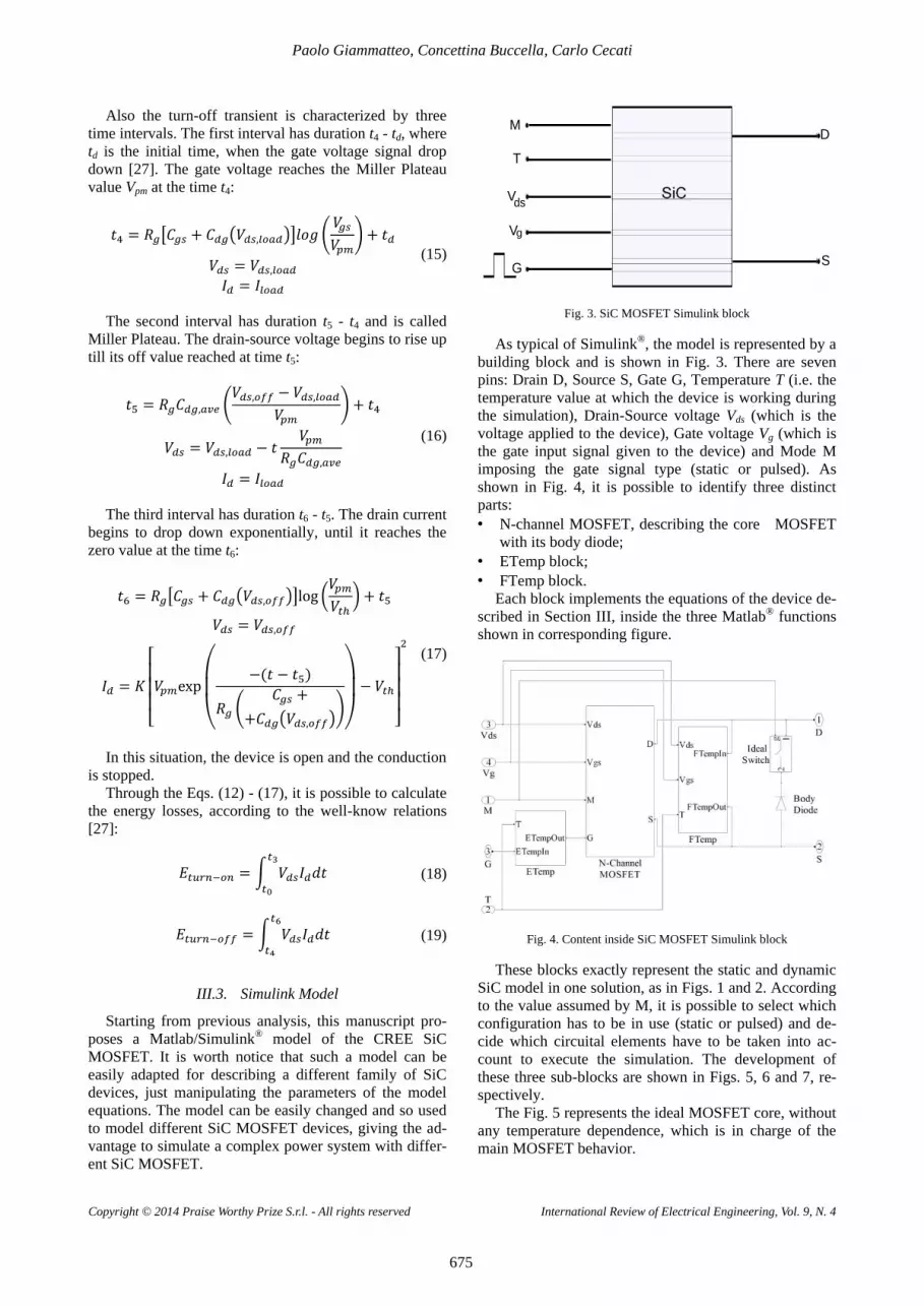
Fig. 3. SiC MOSFET Simulink block
As typical of Simulink®, the model is represented by a
building block and is shown in Fig. 3. There are seven
pins: Drain D, Source S, Gate G, Temperature T (i.e. the
temperature value at which the device is working during
the simulation), Drain-Source voltage Vds (which is the
voltage applied to the device), Gate voltage Vg (which is
the gate input signal given to the device) and Mode M
imposing the gate signal type (static or pulsed). As
shown in Fig. 4, it is possible to identify three distinct
parts:
• N-channel MOSFET, describing the core MOSFET
with its body diode;
• ETemp block;
• FTemp block.
Each block implements the equations of the device de-
scribed in Section III, inside the three Matlab® functions
shown in corresponding figure.
Fig. 4. Content inside SiC MOSFET Simulink block
These blocks exactly represent the static and dynamic
SiC model in one solution, as in Figs. 1 and 2. According
to the value assumed by M, it is possible to select which
configuration has to be in use (static or pulsed) and de-
cide which circuital elements have to be taken into ac-
count to execute the simulation. The development of
these three sub-blocks are shown in Figs. 5, 6 and 7, re-
spectively.
The Fig. 5 represents the ideal MOSFET core, without
any temperature dependence, which is in charge of the
main MOSFET behavior.
G
T
MD
S
dsV
gV

Copyright © 2014 Praise Worthy Prize S.r.l.
account all the aspect of the device, static and dynamic, and it is inspired to the MOSFET circuit shown in [18], with some little modifthere is the develothe MOSFET.
tively the voltage and current generators. Each block
Copyright © 2014 Praise Worthy Prize S.r.l.
The circuitaccount all the aspect of the device, static and dynamic, and it is inspired to the MOSFET circuit shown in [18], with some little modifthere is the develothe MOSFET.
On the other hand, the Figs. 6 and 7 represent respetively the voltage and current generators. Each block
Copyright © 2014 Praise Worthy Prize S.r.l.
Fig.
Fig.
The circuital design is deveaccount all the aspect of the device, static and dynamic, and it is inspired to the MOSFET circuit shown in [18], with some little modifthere is the develothe MOSFET.
On the other hand, the Figs. 6 and 7 represent respetively the voltage and current generators. Each block
Copyright © 2014 Praise Worthy Prize S.r.l.
Fig. 6. The voltage generator Etemp
Fig. 7. The current generator Ftemp
al design is deveaccount all the aspect of the device, static and dynamic, and it is inspired to the MOSFET circuit shown in [18], with some little modifthere is the develop
On the other hand, the Figs. 6 and 7 represent respetively the voltage and current generators. Each block
Copyright © 2014 Praise Worthy Prize S.r.l.
Fig. 5. The core block
6. The voltage generator Etemp
7. The current generator Ftemp
al design is deveaccount all the aspect of the device, static and dynamic, and it is inspired to the MOSFET circuit shown in [18], with some little modifi
pment of the equatio
On the other hand, the Figs. 6 and 7 represent respetively the voltage and current generators. Each block
Copyright © 2014 Praise Worthy Prize S.r.l.
Fig. 5. The core block
6. The voltage generator Etemp
7. The current generator Ftemp
al design is deveaccount all the aspect of the device, static and dynamic, and it is inspired to the MOSFET circuit shown in [18],
ication. Inside the Matlab Function ment of the equatio
On the other hand, the Figs. 6 and 7 represent respetively the voltage and current generators. Each block
Copyright © 2014 Praise Worthy Prize S.r.l.
Fig. 5. The core block
6. The voltage generator Etemp
7. The current generator Ftemp
al design is deve
account all the aspect of the device, static and dynamic, and it is inspired to the MOSFET circuit shown in [18],
cation. Inside the Matlab Function ment of the equatio
On the other hand, the Figs. 6 and 7 represent respetively the voltage and current generators. Each block
Paolo Giammatteo
Copyright © 2014 Praise Worthy Prize S.r.l.
Fig. 5. The core block
6. The voltage generator Etemp
7. The current generator Ftemp
al design is developed in order to take into
account all the aspect of the device, static and dynamic, and it is inspired to the MOSFET circuit shown in [18],
cation. Inside the Matlab Function ment of the equatio
On the other hand, the Figs. 6 and 7 represent respetively the voltage and current generators. Each block
Paolo Giammatteo
Copyright © 2014 Praise Worthy Prize S.r.l. -
Fig. 5. The core block
6. The voltage generator Etemp
7. The current generator Ftemp
oped in order to take into account all the aspect of the device, static and dynamic, and it is inspired to the MOSFET circuit shown in [18],
cation. Inside the Matlab Function ment of the equatio
On the other hand, the Figs. 6 and 7 represent respetively the voltage and current generators. Each block
Paolo Giammatteo
- All rights reserved
Fig. 5. The core block
6. The voltage generator Etemp
7. The current generator Ftemp
oped in order to take into account all the aspect of the device, static and dynamic, and it is inspired to the MOSFET circuit shown in [18],
cation. Inside the Matlab Function ment of the equatio
On the other hand, the Figs. 6 and 7 represent respetively the voltage and current generators. Each block
Paolo Giammatteo
All rights reserved
6. The voltage generator Etemp
7. The current generator Ftemp
oped in order to take into account all the aspect of the device, static and dynamic, and it is inspired to the MOSFET circuit shown in [18],
cation. Inside the Matlab Function ment of the equations which describe
On the other hand, the Figs. 6 and 7 represent respetively the voltage and current generators. Each block
Paolo Giammatteo
All rights reserved
6. The voltage generator Etemp
7. The current generator Ftemp
oped in order to take into account all the aspect of the device, static and dynamic, and it is inspired to the MOSFET circuit shown in [18],
cation. Inside the Matlab Function ns which describe
On the other hand, the Figs. 6 and 7 represent respetively the voltage and current generators. Each block
Paolo Giammatteo
All rights reserved
oped in order to take into account all the aspect of the device, static and dynamic, and it is inspired to the MOSFET circuit shown in [18],
cation. Inside the Matlab Function ns which describe
On the other hand, the Figs. 6 and 7 represent respetively the voltage and current generators. Each block
Paolo Giammatteo, C
All rights reserved
oped in order to take into account all the aspect of the device, static and dynamic, and it is inspired to the MOSFET circuit shown in [18],
cation. Inside the Matlab Function ns which describe
On the other hand, the Figs. 6 and 7 represent respetively the voltage and current generators. Each block
, Concettina Buccella
All rights reserved
oped in order to take into account all the aspect of the device, static and dynamic, and it is inspired to the MOSFET circuit shown in [18],
cation. Inside the Matlab Function ns which describe
On the other hand, the Figs. 6 and 7 represent respec-tively the voltage and current generators. Each block
oncettina Buccella
All rights reserved
676
oped in order to take into account all the aspect of the device, static and dynamic, and it is inspired to the MOSFET circuit shown in [18],
cation. Inside the Matlab Function ns which describe
c-tively the voltage and current generators. Each block
oncettina Buccella
All rights reserved
676
consists of a generator which, according to the input vaues, impose respectively the correct output voltage and currenwritten inside the Matlab Function box.
MOSFET was validated comparing the tic the manufacturer [16].
[10and 10 show the trized for applied voltage gate V125 between simulated and experimental curves obtained at low values of draintive p11, 12 and 13. It is possible to denote that the errors, in the linear region, decrease when the temperature increaes.
for = 75 percentage error in the linear region are explainable oserving that in thetance is small and the channel resistance is high, copared tmore significant contr
This results in the gradual transition from the linear rgion to the saturation region of the SiC cu
the turncording to Eqs. (18) and (19). The model was simulated under the conditions 20Fig
time obtained by simulation using the proposed model present a good agreement with the mshown in Table II.
[25],ment between computed and manufacturer data can be observed.
oncettina Buccella
All rights reserved
consists of a generator which, according to the input vaues, impose respectively the correct output voltage and currenwritten inside the Matlab Function box.
The proposed Simulink/MatlabMOSFET was validated comparing the tic curves obtained bythe manufacturer [16].
The validity intervals of the model for [10]and 10 show the trized for applied voltage gate Vg = 18 125 between simulated and experimental curves obtained at low values of draintive p11, 12 and 13. It is possible to denote that the errors, in the linear region, decrease when the temperature increaes.
Fig. 14 shows the same characteristic curves evaluated for V= 75 percentage error in the linear region are explainable oserving that in thetance is small and the channel resistance is high, copared tmore significant contr
This is due to the low channel surface mobility of SiC. This results in the gradual transition from the linear rgion to the saturation region of the SiC cu
The energy switching losses of the SiC device during the turncording to Eqs. (18) and (19). The model was simulated under the conditions 20A Figs
Through them, it is possible to obtain both the rise time obtained by simulation using the proposed model present a good agreement with the mshown in Table II.
The energy switching losses are evaluated for
[25],ment between computed and manufacturer data can be observed.
oncettina Buccella
consists of a generator which, according to the input vaues, impose respectively the correct output voltage and current to the generators, through the Eqs. (8) and (11) written inside the Matlab Function box.
The proposed Simulink/MatlabMOSFET was validated comparing the
curves obtained bythe manufacturer [16].
The validity intervals of the model for ] – [
and 10 show the trized for applied voltage gate
= 18 125 °Cbetween simulated and experimental curves obtained at low values of draintive percentage errors 11, 12 and 13. It is possible to denote that the errors, in the linear region, decrease when the temperature increa
Fig. 14 shows the same characteristic curves evaluated Vg = 14
= 75 °Cpercentage error in the linear region are explainable oserving that in thetance is small and the channel resistance is high, copared to the model, thus making the MOSFET channel a more significant contr
This is due to the low channel surface mobility of SiC. This results in the gradual transition from the linear rgion to the saturation region of the SiC cu
The energy switching losses of the SiC device during the turncording to Eqs. (18) and (19). The model was simulated under the conditions
A and s. 15.Through them, it is possible to obtain both the rise
time triseobtained by simulation using the proposed model present a good agreement with the mshown in Table II.
The energy switching losses are evaluated for
[25], [125] ment between computed and manufacturer data can be observed.
oncettina Buccella
International Review of Electrical Engineering, Vol. 9, N. 4
consists of a generator which, according to the input vaues, impose respectively the correct output voltage and
t to the generators, through the Eqs. (8) and (11) written inside the Matlab Function box.
III.4.
The proposed Simulink/MatlabMOSFET was validated comparing the
curves obtained bythe manufacturer [16].
The validity intervals of the model for [20]
and 10 show the trized for applied voltage gate
= 18 V C, respectively. In order to point out the difference
between simulated and experimental curves obtained at low values of drain
ercentage errors 11, 12 and 13. It is possible to denote that the errors, in the linear region, decrease when the temperature increa
Fig. 14 shows the same characteristic curves evaluated = 14 C, T
percentage error in the linear region are explainable oserving that in thetance is small and the channel resistance is high, co
o the model, thus making the MOSFET channel a more significant contr
This is due to the low channel surface mobility of SiC. This results in the gradual transition from the linear rgion to the saturation region of the SiC cu
The energy switching losses of the SiC device during the turn-on and the turncording to Eqs. (18) and (19). The model was simulated under the conditions
nd R. 15.
Through them, it is possible to obtain both the rise rise and the fall time
obtained by simulation using the proposed model present a good agreement with the mshown in Table II.
The energy switching losses are evaluated for 125]
ment between computed and manufacturer data can be observed.
oncettina Buccella, Carlo Cecati
International Review of Electrical Engineering, Vol. 9, N. 4
consists of a generator which, according to the input vaues, impose respectively the correct output voltage and
t to the generators, through the Eqs. (8) and (11) written inside the Matlab Function box.
III.4.
The proposed Simulink/MatlabMOSFET was validated comparing the
curves obtained bythe manufacturer [16].
The validity intervals of the model for 20] V
and 10 show the trized for applied voltage gate
V , evaluated at , respectively. In order to point out the difference
between simulated and experimental curves obtained at low values of drain
ercentage errors 11, 12 and 13. It is possible to denote that the errors, in the linear region, decrease when the temperature increa
Fig. 14 shows the same characteristic curves evaluated = 14 V
T =100 percentage error in the linear region are explainable oserving that in thetance is small and the channel resistance is high, co
o the model, thus making the MOSFET channel a more significant contr
This is due to the low channel surface mobility of SiC. This results in the gradual transition from the linear rgion to the saturation region of the SiC cu
IV.The energy switching losses of the SiC device during
on and the turncording to Eqs. (18) and (19). The model was simulated under the conditions
Rg = 6
Through them, it is possible to obtain both the rise and the fall time
obtained by simulation using the proposed model present a good agreement with the mshown in Table II.
The energy switching losses are evaluated for 125] °C
ment between computed and manufacturer data can be
, Carlo Cecati
International Review of Electrical Engineering, Vol. 9, N. 4
consists of a generator which, according to the input vaues, impose respectively the correct output voltage and
t to the generators, through the Eqs. (8) and (11) written inside the Matlab Function box.
Validation of the
The proposed Simulink/MatlabMOSFET was validated comparing the
curves obtained bythe manufacturer [16].
The validity intervals of the model for V and
and 10 show the trized for applied voltage gate
, evaluated at , respectively. In order to point out the difference
between simulated and experimental curves obtained at low values of drain
ercentage errors 11, 12 and 13. It is possible to denote that the errors, in the linear region, decrease when the temperature increa
Fig. 14 shows the same characteristic curves evaluated V, parameterized=100
percentage error in the linear region are explainable oserving that in thetance is small and the channel resistance is high, co
o the model, thus making the MOSFET channel a more significant contr
This is due to the low channel surface mobility of SiC. This results in the gradual transition from the linear rgion to the saturation region of the SiC cu
IV. The energy switching losses of the SiC device during
on and the turncording to Eqs. (18) and (19). The model was simulated under the conditions
= 6,8 Ω
Through them, it is possible to obtain both the rise and the fall time
obtained by simulation using the proposed model present a good agreement with the mshown in Table II.
SIC
Data sourceSimulation
Manufacturer
The energy switching losses are evaluated for C and are shown in Fig. 1
ment between computed and manufacturer data can be
, Carlo Cecati
International Review of Electrical Engineering, Vol. 9, N. 4
consists of a generator which, according to the input vaues, impose respectively the correct output voltage and
t to the generators, through the Eqs. (8) and (11) written inside the Matlab Function box.
Validation of the
The proposed Simulink/MatlabMOSFET was validated comparing the
curves obtained bythe manufacturer [16].
The validity intervals of the model for and [25
and 10 show the Idtrized for applied voltage gate
, evaluated at , respectively. In order to point out the difference
between simulated and experimental curves obtained at low values of drain-source voltage, the drain current rel
ercentage errors 11, 12 and 13. It is possible to denote that the errors, in the linear region, decrease when the temperature increa
Fig. 14 shows the same characteristic curves evaluated , parameterized
=100 °C percentage error in the linear region are explainable oserving that in the SiC MOSFET the epitaxial layer resitance is small and the channel resistance is high, co
o the model, thus making the MOSFET channel a more significant contr
This is due to the low channel surface mobility of SiC. This results in the gradual transition from the linear rgion to the saturation region of the SiC cu
Losses CalculationsThe energy switching losses of the SiC device during
on and the turncording to Eqs. (18) and (19). The model was simulated under the conditions
8 Ω
Through them, it is possible to obtain both the rise and the fall time
obtained by simulation using the proposed model present a good agreement with the mshown in Table II.
MOSFETData sourceSimulation
Manufacturer
The energy switching losses are evaluated for and are shown in Fig. 1
ment between computed and manufacturer data can be
, Carlo Cecati
International Review of Electrical Engineering, Vol. 9, N. 4
consists of a generator which, according to the input vaues, impose respectively the correct output voltage and
t to the generators, through the Eqs. (8) and (11) written inside the Matlab Function box.
Validation of the
The proposed Simulink/MatlabMOSFET was validated comparing the
curves obtained by the manufacturer [16].
The validity intervals of the model for [25] –
d - Vtrized for applied voltage gate
, evaluated at , respectively. In order to point out the difference
between simulated and experimental curves obtained at source voltage, the drain current rel
ercentage errors er 11, 12 and 13. It is possible to denote that the errors, in the linear region, decrease when the temperature increa
Fig. 14 shows the same characteristic curves evaluated , parameterized
C and percentage error in the linear region are explainable o
SiC MOSFET the epitaxial layer resitance is small and the channel resistance is high, co
o the model, thus making the MOSFET channel a more significant contributor to the on
This is due to the low channel surface mobility of SiC. This results in the gradual transition from the linear rgion to the saturation region of the SiC cu
Losses CalculationsThe energy switching losses of the SiC device during
on and the turncording to Eqs. (18) and (19). The model was simulated under the conditions Vds
8 Ω. The transient curves are shown in
Through them, it is possible to obtain both the rise and the fall time
obtained by simulation using the proposed model present a good agreement with the m
MOSFETData sourceSimulation
Manufacturer
The energy switching losses are evaluated for and are shown in Fig. 1
ment between computed and manufacturer data can be
, Carlo Cecati
International Review of Electrical Engineering, Vol. 9, N. 4
consists of a generator which, according to the input vaues, impose respectively the correct output voltage and
t to the generators, through the Eqs. (8) and (11) written inside the Matlab Function box.
Validation of the
The proposed Simulink/MatlabMOSFET was validated comparing the
simulations with those
The validity intervals of the model for – [125] Vds
trized for applied voltage gate , evaluated at T
, respectively. In order to point out the difference between simulated and experimental curves obtained at
source voltage, the drain current relr are evaluated and shown in Figs
11, 12 and 13. It is possible to denote that the errors, in the linear region, decrease when the temperature increa
Fig. 14 shows the same characteristic curves evaluated , parameterized
and T percentage error in the linear region are explainable o
SiC MOSFET the epitaxial layer resitance is small and the channel resistance is high, co
o the model, thus making the MOSFET channel a ibutor to the on
This is due to the low channel surface mobility of SiC. This results in the gradual transition from the linear rgion to the saturation region of the SiC cu
Losses CalculationsThe energy switching losses of the SiC device during
on and the turn-off transients are computed, acording to Eqs. (18) and (19). The model was simulated
Vds,off. The transient curves are shown in
Through them, it is possible to obtain both the rise and the fall time
obtained by simulation using the proposed model present a good agreement with the m
TABLEMOSFET RISE
Data source Simulation
Manufacturer
The energy switching losses are evaluated for and are shown in Fig. 1
ment between computed and manufacturer data can be
International Review of Electrical Engineering, Vol. 9, N. 4
consists of a generator which, according to the input vaues, impose respectively the correct output voltage and
t to the generators, through the Eqs. (8) and (11) written inside the Matlab Function box.
Validation of the
The proposed Simulink/MatlabMOSFET was validated comparing the
simulations with those
The validity intervals of the model for 125] characteristic
trized for applied voltage gate T = 25
, respectively. In order to point out the difference between simulated and experimental curves obtained at
source voltage, the drain current relare evaluated and shown in Figs
11, 12 and 13. It is possible to denote that the errors, in the linear region, decrease when the temperature increa
Fig. 14 shows the same characteristic curves evaluated , parameterized for
T = 125 percentage error in the linear region are explainable o
SiC MOSFET the epitaxial layer resitance is small and the channel resistance is high, co
o the model, thus making the MOSFET channel a ibutor to the on
This is due to the low channel surface mobility of SiC. This results in the gradual transition from the linear rgion to the saturation region of the SiC cu
Losses CalculationsThe energy switching losses of the SiC device during
off transients are computed, acording to Eqs. (18) and (19). The model was simulated
off = 800 . The transient curves are shown in
Through them, it is possible to obtain both the rise and the fall time tfall
obtained by simulation using the proposed model present a good agreement with the m
TABLE
ISE A
The energy switching losses are evaluated for and are shown in Fig. 1
ment between computed and manufacturer data can be
International Review of Electrical Engineering, Vol. 9, N. 4
consists of a generator which, according to the input vaues, impose respectively the correct output voltage and
t to the generators, through the Eqs. (8) and (11) written inside the Matlab Function box.
Validation of the Proposed Model
The proposed Simulink/MatlabMOSFET was validated comparing the
simulations with those
The validity intervals of the model for 125] °C, respec
characteristictrized for applied voltage gate Vg = 10
= 25 °, respectively. In order to point out the difference
between simulated and experimental curves obtained at source voltage, the drain current rel
are evaluated and shown in Figs11, 12 and 13. It is possible to denote that the errors, in the linear region, decrease when the temperature increa
Fig. 14 shows the same characteristic curves evaluated for T
= 125 percentage error in the linear region are explainable o
SiC MOSFET the epitaxial layer resitance is small and the channel resistance is high, co
o the model, thus making the MOSFET channel a ibutor to the on
This is due to the low channel surface mobility of SiC. This results in the gradual transition from the linear rgion to the saturation region of the SiC cu
Losses CalculationsThe energy switching losses of the SiC device during
off transients are computed, acording to Eqs. (18) and (19). The model was simulated
= 800 . The transient curves are shown in
Through them, it is possible to obtain both the rise of the device. The va
obtained by simulation using the proposed model present a good agreement with the m
TABLE II AND
trise
The energy switching losses are evaluated for and are shown in Fig. 1
ment between computed and manufacturer data can be
International Review of Electrical Engineering, Vol. 9, N. 4
consists of a generator which, according to the input vaues, impose respectively the correct output voltage and
t to the generators, through the Eqs. (8) and (11) written inside the Matlab Function box.
Proposed Model
The proposed Simulink/Matlab® model of the 4HMOSFET was validated comparing the
simulations with those
The validity intervals of the model for , respec
characteristic= 10 °C; T
, respectively. In order to point out the difference between simulated and experimental curves obtained at
source voltage, the drain current relare evaluated and shown in Figs
11, 12 and 13. It is possible to denote that the errors, in the linear region, decrease when the temperature increa
Fig. 14 shows the same characteristic curves evaluated T = 25
= 125 °C.percentage error in the linear region are explainable o
SiC MOSFET the epitaxial layer resitance is small and the channel resistance is high, co
o the model, thus making the MOSFET channel a ibutor to the on
This is due to the low channel surface mobility of SiC. This results in the gradual transition from the linear rgion to the saturation region of the SiC cu
Losses CalculationsThe energy switching losses of the SiC device during
off transients are computed, acording to Eqs. (18) and (19). The model was simulated
= 800 V, . The transient curves are shown in
Through them, it is possible to obtain both the rise of the device. The va
obtained by simulation using the proposed model present a good agreement with the manufacturer values, as
ND FALL
rise(ns)12,313,6
The energy switching losses are evaluated for and are shown in Fig. 1
ment between computed and manufacturer data can be
International Review of Electrical Engineering, Vol. 9, N. 4
consists of a generator which, according to the input vaues, impose respectively the correct output voltage and
t to the generators, through the Eqs. (8) and (11) written inside the Matlab Function box.
Proposed Model
model of the 4HMOSFET was validated comparing the I
simulations with those
The validity intervals of the model for , respec
characteristic= 10 V C; T = 75
, respectively. In order to point out the difference between simulated and experimental curves obtained at
source voltage, the drain current relare evaluated and shown in Figs
11, 12 and 13. It is possible to denote that the errors, in the linear region, decrease when the temperature increa
Fig. 14 shows the same characteristic curves evaluated = 25
. The high values of percentage error in the linear region are explainable o
SiC MOSFET the epitaxial layer resitance is small and the channel resistance is high, co
o the model, thus making the MOSFET channel a ibutor to the on-state voltage.
This is due to the low channel surface mobility of SiC. This results in the gradual transition from the linear rgion to the saturation region of the SiC cu
Losses CalculationsThe energy switching losses of the SiC device during
off transients are computed, acording to Eqs. (18) and (19). The model was simulated
, Vg. The transient curves are shown in
Through them, it is possible to obtain both the rise of the device. The va
obtained by simulation using the proposed model present anufacturer values, as
ALL TIMES(ns)
12,3 13,6
The energy switching losses are evaluated for and are shown in Fig. 16. A good agre
ment between computed and manufacturer data can be
International Review of Electrical Engineering, Vol. 9, N. 4
consists of a generator which, according to the input vaues, impose respectively the correct output voltage and
t to the generators, through the Eqs. (8) and (11)
Proposed Model
model of the 4HId-Vds
simulations with those
The validity intervals of the model for V, respectively. Fig
characteristic curves paramV , V= 75
, respectively. In order to point out the difference between simulated and experimental curves obtained at
source voltage, the drain current relare evaluated and shown in Figs
11, 12 and 13. It is possible to denote that the errors, in the linear region, decrease when the temperature increa
Fig. 14 shows the same characteristic curves evaluated = 25 °C, T
The high values of percentage error in the linear region are explainable o
SiC MOSFET the epitaxial layer resitance is small and the channel resistance is high, co
o the model, thus making the MOSFET channel a state voltage.
This is due to the low channel surface mobility of SiC. This results in the gradual transition from the linear rgion to the saturation region of the SiC curves.
Losses CalculationsThe energy switching losses of the SiC device during
off transients are computed, acording to Eqs. (18) and (19). The model was simulated
g = 20 . The transient curves are shown in
Through them, it is possible to obtain both the rise of the device. The va
obtained by simulation using the proposed model present anufacturer values, as
IMES tfall(ns)35,435,6
The energy switching losses are evaluated for 6. A good agre
ment between computed and manufacturer data can be
International Review of Electrical Engineering, Vol. 9, N. 4
consists of a generator which, according to the input vaues, impose respectively the correct output voltage and
t to the generators, through the Eqs. (8) and (11)
Proposed Model
model of the 4HVds characteri
simulations with those
Vgs tively. Figcurves paramVg = 14
= 75 °C , respectively. In order to point out the difference
between simulated and experimental curves obtained at source voltage, the drain current rel
are evaluated and shown in Figs11, 12 and 13. It is possible to denote that the errors, in the linear region, decrease when the temperature increa
Fig. 14 shows the same characteristic curves evaluated C, T = 50
The high values of percentage error in the linear region are explainable o
SiC MOSFET the epitaxial layer resitance is small and the channel resistance is high, co
o the model, thus making the MOSFET channel a state voltage.
This is due to the low channel surface mobility of SiC. This results in the gradual transition from the linear r
rves.
Losses Calculations The energy switching losses of the SiC device during
off transients are computed, acording to Eqs. (18) and (19). The model was simulated
= 20 . The transient curves are shown in
Through them, it is possible to obtain both the rise of the device. The va
obtained by simulation using the proposed model present anufacturer values, as
(ns)
35,4 35,6
The energy switching losses are evaluated for 6. A good agre
ment between computed and manufacturer data can be
International Review of Electrical Engineering, Vol. 9, N. 4
consists of a generator which, according to the input vaues, impose respectively the correct output voltage and
t to the generators, through the Eqs. (8) and (11)
Proposed Model
model of the 4Hcharacteri
simulations with those given by
and tively. Figcurves param
= 14 C and
, respectively. In order to point out the difference between simulated and experimental curves obtained at
source voltage, the drain current relare evaluated and shown in Figs
11, 12 and 13. It is possible to denote that the errors, in the linear region, decrease when the temperature increa
Fig. 14 shows the same characteristic curves evaluated = 50
The high values of percentage error in the linear region are explainable o
SiC MOSFET the epitaxial layer resitance is small and the channel resistance is high, co
o the model, thus making the MOSFET channel a state voltage.
This is due to the low channel surface mobility of SiC. This results in the gradual transition from the linear r
The energy switching losses of the SiC device during off transients are computed, a
cording to Eqs. (18) and (19). The model was simulated = 20 V,
. The transient curves are shown in
Through them, it is possible to obtain both the rise of the device. The va
obtained by simulation using the proposed model present anufacturer values, as
The energy switching losses are evaluated for T inside 6. A good agre
ment between computed and manufacturer data can be
International Review of Electrical Engineering, Vol. 9, N. 4
consists of a generator which, according to the input vaues, impose respectively the correct output voltage and
t to the generators, through the Eqs. (8) and (11)
model of the 4H-SiC characteri
given by
and T tively. Figs. 8, 9 curves param
= 14 V and and T
, respectively. In order to point out the difference between simulated and experimental curves obtained at
source voltage, the drain current relare evaluated and shown in Figs
11, 12 and 13. It is possible to denote that the errors, in the linear region, decrease when the temperature increa
Fig. 14 shows the same characteristic curves evaluated = 50 °C
The high values of percentage error in the linear region are explainable o
SiC MOSFET the epitaxial layer resitance is small and the channel resistance is high, co
o the model, thus making the MOSFET channel a state voltage.
This is due to the low channel surface mobility of SiC. This results in the gradual transition from the linear r
The energy switching losses of the SiC device during off transients are computed, a
cording to Eqs. (18) and (19). The model was simulated , Iload
. The transient curves are shown in
Through them, it is possible to obtain both the rise of the device. The val
obtained by simulation using the proposed model present anufacturer values, as
T inside 6. A good agre
ment between computed and manufacturer data can be
International Review of Electrical Engineering, Vol. 9, N. 4
consists of a generator which, according to the input val-ues, impose respectively the correct output voltage and
t to the generators, through the Eqs. (8) and (11)
SiC characteris-
given by
T are 8, 9
curves parame-and T =
, respectively. In order to point out the difference between simulated and experimental curves obtained at
source voltage, the drain current rela-are evaluated and shown in Figs.
11, 12 and 13. It is possible to denote that the errors, in the linear region, decrease when the temperature increas-
Fig. 14 shows the same characteristic curves evaluated C ,T
The high values of percentage error in the linear region are explainable ob-
SiC MOSFET the epitaxial layer resis-tance is small and the channel resistance is high, com-
o the model, thus making the MOSFET channel a
This is due to the low channel surface mobility of SiC. This results in the gradual transition from the linear re-
The energy switching losses of the SiC device during off transients are computed, ac-
cording to Eqs. (18) and (19). The model was simulated load =
. The transient curves are shown in
Through them, it is possible to obtain both the rise lues
obtained by simulation using the proposed model present anufacturer values, as
T inside 6. A good agree-
ment between computed and manufacturer data can be
International Review of Electrical Engineering, Vol. 9, N. 4
l-ues, impose respectively the correct output voltage and
t to the generators, through the Eqs. (8) and (11)
SiC s-
given by
are 8, 9
e-and
= , respectively. In order to point out the difference
between simulated and experimental curves obtained at a-
. 11, 12 and 13. It is possible to denote that the errors, in
s-
Fig. 14 shows the same characteristic curves evaluated T
The high values of b-s-
m-o the model, thus making the MOSFET channel a
This is due to the low channel surface mobility of SiC. e-
The energy switching losses of the SiC device during c-
cording to Eqs. (18) and (19). The model was simulated =
. The transient curves are shown in
Through them, it is possible to obtain both the rise ues
obtained by simulation using the proposed model present anufacturer values, as
T inside e-
ment between computed and manufacturer data can be

Copyright © 2014 Praise Worthy Prize S.r.l. Copyright © 2014 Praise Worthy Prize S.r.l.
Fig. 10.
Copyright © 2014 Praise Worthy Prize S.r.l.
Fig. 8.
Fig. 9.
Fig. 10.
Fig. 11.
Copyright © 2014 Praise Worthy Prize S.r.l.
Fig. 8. Id
Fig. 9. Id
Fig. 10. Id
Fig. 11. and expe
Copyright © 2014 Praise Worthy Prize S.r.l.
d-Vds
d-Vds
d-Vds
Fig. 11. Relative percentage error between the simulatedand expe
Copyright © 2014 Praise Worthy Prize S.r.l.
ds characteristic
ds characteristic
ds characteristic
Relative percentage error between the simulatedand expe
Copyright © 2014 Praise Worthy Prize S.r.l.
characteristic
characteristic
characteristic
Relative percentage error between the simulatedand experimental curves shown in Fig. 8
Copyright © 2014 Praise Worthy Prize S.r.l.
characteristic
characteristic
characteristic
Relative percentage error between the simulatedrimental curves shown in Fig. 8
Copyright © 2014 Praise Worthy Prize S.r.l.
characteristic curves evaluated at
characteristic curves evaluated at
characteristic curves evaluated
Relative percentage error between the simulated
rimental curves shown in Fig. 8
Paolo Giammatteo
Copyright © 2014 Praise Worthy Prize S.r.l.
curves evaluated at
curves evaluated at
curves evaluated
Relative percentage error between the simulated
rimental curves shown in Fig. 8
Paolo Giammatteo
Copyright © 2014 Praise Worthy Prize S.r.l. -
curves evaluated at
curves evaluated at
curves evaluated
Relative percentage error between the simulatedrimental curves shown in Fig. 8
Paolo Giammatteo
- All rights reserved
curves evaluated at
curves evaluated at
curves evaluated
Relative percentage error between the simulatedrimental curves shown in Fig. 8
Paolo Giammatteo
All rights reserved
curves evaluated at
curves evaluated at
curves evaluated at
Relative percentage error between the simulatedrimental curves shown in Fig. 8
Paolo Giammatteo
All rights reserved
curves evaluated at T = 25
curves evaluated at T = 75
at T = 125
Relative percentage error between the simulatedrimental curves shown in Fig. 8
Paolo Giammatteo
All rights reserved
= 25 °
= 75 °
= 125
Relative percentage error between the simulated
Paolo Giammatteo, C
All rights reserved
°C
°C
= 125 °C
Relative percentage error between the simulated
, Concettina Buccella
All rights reserved
oncettina Buccella
All rights reserved
677
oncettina Buccella
All rights reserved
677
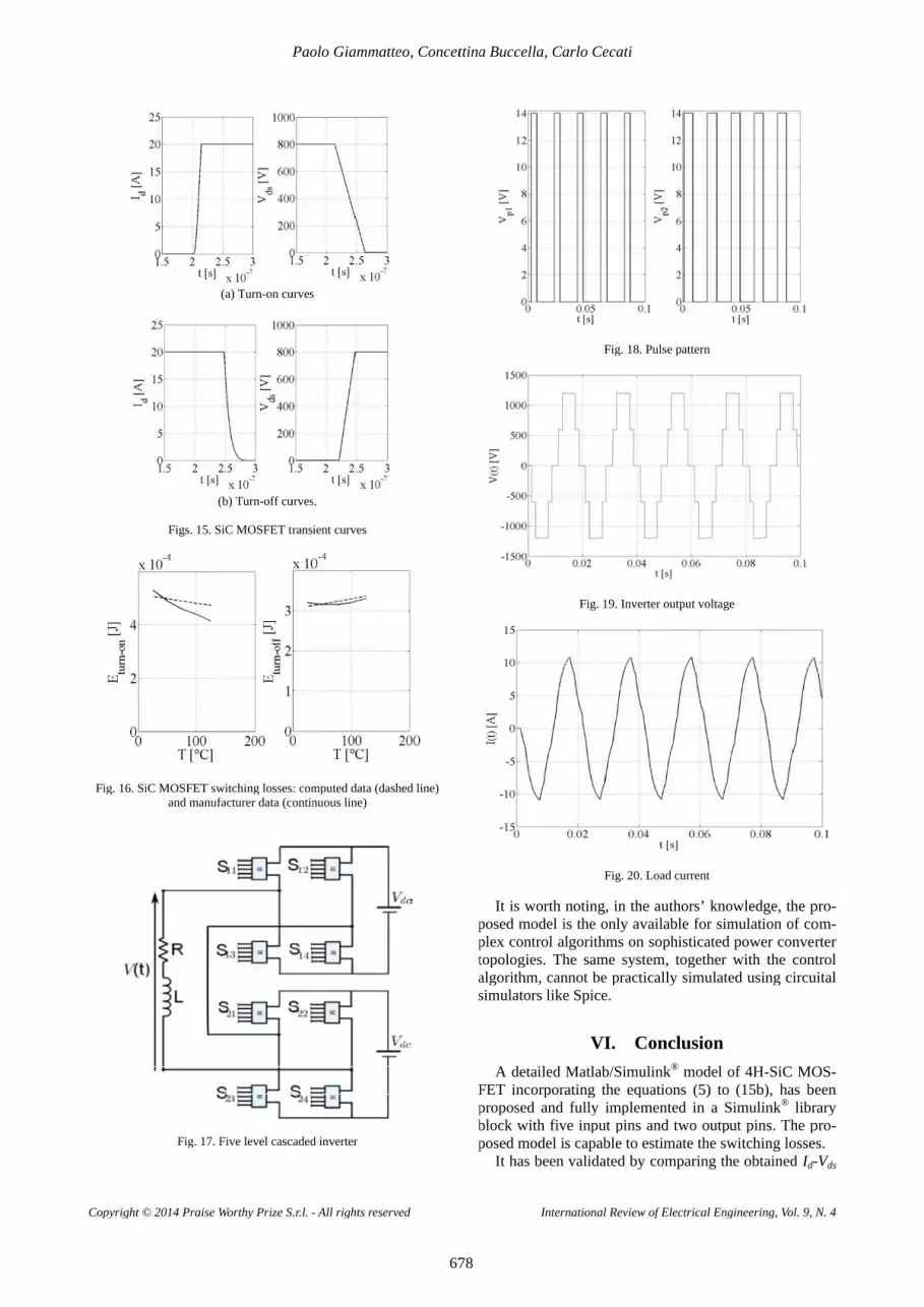
lab/Simulinkcomplex devices, in Fig. 17 has been considered.lation results are obtained at two different temperature: TkV AL monic elimination algorithm, for modulation index 0.8on load, evaluated at 20, respectively.
oncettina Buccella
All rights reserved
In order to show the versatility of the Malab/Simulinkcomplex devices, in Fig. 17 has been considered.lation results are obtained at two different temperature: T1 = 50kV AL = 0monic elimination algorithm, for modulation index 0.8, is shown in Fig. 18 [28]. Output voltage and current on load, evaluated at 20, respectively.
oncettina Buccella
Fig. 12.
Fig. 13.
Fig
In order to show the versatility of the Malab/Simulinkcomplex devices, in Fig. 17 has been considered.lation results are obtained at two different temperature:
= 50kV A, V
= 0.2 monic elimination algorithm, for modulation index
, is shown in Fig. 18 [28]. Output voltage and current on load, evaluated at 20, respectively.
oncettina Buccella
International Review of Electrical Engineering, Vol. 9, N. 4
Fig. 12.
Fig. 13.
Fig. 14.
In order to show the versatility of the Malab/Simulinkcomplex devices, in Fig. 17 has been considered.lation results are obtained at two different temperature:
= 50°C and Vdc 2 H.
monic elimination algorithm, for modulation index , is shown in Fig. 18 [28]. Output voltage and current
on load, evaluated at 20, respectively.
oncettina Buccella, Carlo Cecati
International Review of Electrical Engineering, Vol. 9, N. 4
Fig. 12. Relative percentage error between the simulatedand experimental curves shown in Fig. 9
Fig. 13. Relative percentage error beand experimental curves shown in Fig. 10
. 14. Id-
V.In order to show the versatility of the Ma
lab/Simulink®
complex devices, in Fig. 17 has been considered.lation results are obtained at two different temperature:
°C and = 600
H. The pulse pattern, obtained by using the hamonic elimination algorithm, for modulation index
, is shown in Fig. 18 [28]. Output voltage and current on load, evaluated at 20, respectively.
, Carlo Cecati
International Review of Electrical Engineering, Vol. 9, N. 4
Relative percentage error between the simulatedand experimental curves shown in Fig. 9
Relative percentage error beand experimental curves shown in Fig. 10
-Vds characteristic curves evaluated for
V. In order to show the versatility of the Ma
® SiC MOSFET model to compose more complex devices, in Fig. 17 has been considered.lation results are obtained at two different temperature:
°C and T= 600 The pulse pattern, obtained by using the ha
monic elimination algorithm, for modulation index , is shown in Fig. 18 [28]. Output voltage and current
on load, evaluated at 20, respectively.
, Carlo Cecati
International Review of Electrical Engineering, Vol. 9, N. 4
Relative percentage error between the simulatedand experimental curves shown in Fig. 9
Relative percentage error beand experimental curves shown in Fig. 10
characteristic curves evaluated for
Application ExampleIn order to show the versatility of the Ma
SiC MOSFET model to compose more complex devices, the five level cascaded inverter shown in Fig. 17 has been considered.lation results are obtained at two different temperature:
T2 = 100= 600 V and a RThe pulse pattern, obtained by using the ha
monic elimination algorithm, for modulation index , is shown in Fig. 18 [28]. Output voltage and current
on load, evaluated at
, Carlo Cecati
International Review of Electrical Engineering, Vol. 9, N. 4
Relative percentage error between the simulatedand experimental curves shown in Fig. 9
Relative percentage error beand experimental curves shown in Fig. 10
characteristic curves evaluated for
Application ExampleIn order to show the versatility of the Ma
SiC MOSFET model to compose more the five level cascaded inverter shown
in Fig. 17 has been considered.lation results are obtained at two different temperature:
= 100and a R
The pulse pattern, obtained by using the hamonic elimination algorithm, for modulation index
, is shown in Fig. 18 [28]. Output voltage and current on load, evaluated at T = 50
, Carlo Cecati
International Review of Electrical Engineering, Vol. 9, N. 4
Relative percentage error between the simulatedand experimental curves shown in Fig. 9
Relative percentage error beand experimental curves shown in Fig. 10
characteristic curves evaluated for
Application ExampleIn order to show the versatility of the Ma
SiC MOSFET model to compose more the five level cascaded inverter shown
in Fig. 17 has been considered.lation results are obtained at two different temperature:
= 100°C, for rated power equal to and a R
The pulse pattern, obtained by using the hamonic elimination algorithm, for modulation index
, is shown in Fig. 18 [28]. Output voltage and current = 50
International Review of Electrical Engineering, Vol. 9, N. 4
Relative percentage error between the simulatedand experimental curves shown in Fig. 9
Relative percentage error be
and experimental curves shown in Fig. 10
characteristic curves evaluated for
Application ExampleIn order to show the versatility of the Ma
SiC MOSFET model to compose more the five level cascaded inverter shown
in Fig. 17 has been considered.lation results are obtained at two different temperature:
°C, for rated power equal to and a R-L load having
The pulse pattern, obtained by using the hamonic elimination algorithm, for modulation index
, is shown in Fig. 18 [28]. Output voltage and current = 50°C, are shown in Figs. 19 and
International Review of Electrical Engineering, Vol. 9, N. 4
Relative percentage error between the simulatedand experimental curves shown in Fig. 9
Relative percentage error beand experimental curves shown in Fig. 10
characteristic curves evaluated for
Application ExampleIn order to show the versatility of the Ma
SiC MOSFET model to compose more the five level cascaded inverter shown
in Fig. 17 has been considered. For this device the simlation results are obtained at two different temperature:
°C, for rated power equal to L load having
The pulse pattern, obtained by using the hamonic elimination algorithm, for modulation index
, is shown in Fig. 18 [28]. Output voltage and current °C, are shown in Figs. 19 and
International Review of Electrical Engineering, Vol. 9, N. 4
Relative percentage error between the simulatedand experimental curves shown in Fig. 9
Relative percentage error between the simulatedand experimental curves shown in Fig. 10
characteristic curves evaluated for
Application ExampleIn order to show the versatility of the Ma
SiC MOSFET model to compose more the five level cascaded inverter shown
For this device the simlation results are obtained at two different temperature:
°C, for rated power equal to L load having
The pulse pattern, obtained by using the hamonic elimination algorithm, for modulation index
, is shown in Fig. 18 [28]. Output voltage and current °C, are shown in Figs. 19 and
International Review of Electrical Engineering, Vol. 9, N. 4
Relative percentage error between the simulatedand experimental curves shown in Fig. 9
tween the simulatedand experimental curves shown in Fig. 10
characteristic curves evaluated for
Application ExampleIn order to show the versatility of the Ma
SiC MOSFET model to compose more the five level cascaded inverter shown
For this device the simlation results are obtained at two different temperature:
°C, for rated power equal to L load having R
The pulse pattern, obtained by using the hamonic elimination algorithm, for modulation index
, is shown in Fig. 18 [28]. Output voltage and current °C, are shown in Figs. 19 and
International Review of Electrical Engineering, Vol. 9, N. 4
Relative percentage error between the simulatedand experimental curves shown in Fig. 9
tween the simulatedand experimental curves shown in Fig. 10
characteristic curves evaluated for Vg =14
Application Example In order to show the versatility of the Ma
SiC MOSFET model to compose more the five level cascaded inverter shown
For this device the simlation results are obtained at two different temperature:
°C, for rated power equal to R = 102Ω
The pulse pattern, obtained by using the hamonic elimination algorithm, for modulation index
, is shown in Fig. 18 [28]. Output voltage and current °C, are shown in Figs. 19 and
International Review of Electrical Engineering, Vol. 9, N. 4
Relative percentage error between the simulated
tween the simulated
=14
In order to show the versatility of the MaSiC MOSFET model to compose more
the five level cascaded inverter shown For this device the sim
lation results are obtained at two different temperature: °C, for rated power equal to
= 102Ω The pulse pattern, obtained by using the ha
monic elimination algorithm, for modulation index , is shown in Fig. 18 [28]. Output voltage and current
°C, are shown in Figs. 19 and
International Review of Electrical Engineering, Vol. 9, N. 4
Relative percentage error between the simulated
tween the simulated
=14 V
In order to show the versatility of the MaSiC MOSFET model to compose more
the five level cascaded inverter shown For this device the sim
lation results are obtained at two different temperature: °C, for rated power equal to
= 102Ω and The pulse pattern, obtained by using the ha
monic elimination algorithm, for modulation index m, is shown in Fig. 18 [28]. Output voltage and current
°C, are shown in Figs. 19 and
International Review of Electrical Engineering, Vol. 9, N. 4
In order to show the versatility of the Mat-SiC MOSFET model to compose more
the five level cascaded inverter shown For this device the simu-
lation results are obtained at two different temperature: °C, for rated power equal to 12
and The pulse pattern, obtained by using the har-
m1 = , is shown in Fig. 18 [28]. Output voltage and current
°C, are shown in Figs. 19 and
International Review of Electrical Engineering, Vol. 9, N. 4
t-SiC MOSFET model to compose more
the five level cascaded inverter shown u-
lation results are obtained at two different temperature: 12
and r-=
, is shown in Fig. 18 [28]. Output voltage and current °C, are shown in Figs. 19 and
Copyright © 2014 Praise Worthy Prize S.r.l.
Fig.
Copyright © 2014 Praise Worthy Prize S.r.l.
Fig. 16
Copyright © 2014 Praise Worthy Prize S.r.l.
16. SiC MOSFET switching losses: computed data (dashed line)
Copyright © 2014 Praise Worthy Prize S.r.l.
SiC MOSFET switching losses: computed data (dashed line)
Copyright © 2014 Praise Worthy Prize S.r.l.
Figs. 15.
SiC MOSFET switching losses: computed data (dashed line) and manu
Fig
Copyright © 2014 Praise Worthy Prize S.r.l.
s. 15.
SiC MOSFET switching losses: computed data (dashed line) and manu
Fig. 17
Copyright © 2014 Praise Worthy Prize S.r.l.
(a) T
(b) Turn
s. 15. SiC MOSFET transient curves
SiC MOSFET switching losses: computed data (dashed line) and manufacturer data (continuous line)
17. Five level cascaded inverter
Copyright © 2014 Praise Worthy Prize S.r.l.
(a) Turn
(b) Turn
SiC MOSFET transient curves
SiC MOSFET switching losses: computed data (dashed line) facturer data (continuous line)
Five level cascaded inverter
Copyright © 2014 Praise Worthy Prize S.r.l.
urn-on curves
(b) Turn-off curves.
SiC MOSFET transient curves
SiC MOSFET switching losses: computed data (dashed line)
facturer data (continuous line)
Five level cascaded inverter
Paolo Giammatteo
Copyright © 2014 Praise Worthy Prize S.r.l.
on curves
off curves.
SiC MOSFET transient curves
SiC MOSFET switching losses: computed data (dashed line)
facturer data (continuous line)
Five level cascaded inverter
Paolo Giammatteo
Copyright © 2014 Praise Worthy Prize S.r.l. -
on curves
off curves.
SiC MOSFET transient curves
SiC MOSFET switching losses: computed data (dashed line) facturer data (continuous line)
Five level cascaded inverter
Paolo Giammatteo
- All rights reserved
on curves
off curves.
SiC MOSFET transient curves
SiC MOSFET switching losses: computed data (dashed line) facturer data (continuous line)
Five level cascaded inverter
Paolo Giammatteo
All rights reserved
SiC MOSFET transient curves
SiC MOSFET switching losses: computed data (dashed line) facturer data (continuous line)
Five level cascaded inverter
Paolo Giammatteo
All rights reserved
SiC MOSFET transient curves
SiC MOSFET switching losses: computed data (dashed line) facturer data (continuous line)
Five level cascaded inverter
Paolo Giammatteo
All rights reserved
SiC MOSFET switching losses: computed data (dashed line)
Paolo Giammatteo, C
All rights reserved
SiC MOSFET switching losses: computed data (dashed line)
, Concettina Buccella
All rights reserved
SiC MOSFET switching losses: computed data (dashed line)
oncettina Buccella
All rights reserved
678
SiC MOSFET switching losses: computed data (dashed line)
oncettina Buccella
All rights reserved
678
posed model is the only available for simulation of coplex control algorithms on sophisticated power converter topologies.as
FET incorporating the equations (5) to (15b), has been proposed and fully implemenblock with five input pins and two output pins. The prposed model is capable to estimate the switching losses.
oncettina Buccella
All rights reserved
It is worth noting, in the authors’ knowledge, the prposed model is the only available for simulation of coplex control algorithms on sophisticated power converter topologies.algorithm, cannot be practically simsimulators like Spice.
A detailed Matlab/SimulinkFET incorporating the equations (5) to (15b), has been proposed and fully implemenblock with five input pins and two output pins. The prposed model is capable to estimate the switching losses.
It has been validated by comparing the obtained
oncettina Buccella
It is worth noting, in the authors’ knowledge, the prposed model is the only available for simulation of coplex control algorithms on sophisticated power converter topologies.
gorithm, cannot be practically simmulators like Spice.
A detailed Matlab/SimulinkFET incorporating the equations (5) to (15b), has been proposed and fully implemenblock with five input pins and two output pins. The prposed model is capable to estimate the switching losses.
It has been validated by comparing the obtained
oncettina Buccella
International Review of Electrical Engineering, Vol. 9, N. 4
It is worth noting, in the authors’ knowledge, the prposed model is the only available for simulation of coplex control algorithms on sophisticated power converter topologies.
gorithm, cannot be practically simmulators like Spice.
A detailed Matlab/SimulinkFET incorporating the equations (5) to (15b), has been proposed and fully implemenblock with five input pins and two output pins. The prposed model is capable to estimate the switching losses.
It has been validated by comparing the obtained
oncettina Buccella, Carlo Cecati
International Review of Electrical Engineering, Vol. 9, N. 4
It is worth noting, in the authors’ knowledge, the prposed model is the only available for simulation of coplex control algorithms on sophisticated power converter topologies. The same syst
gorithm, cannot be practically simmulators like Spice.
A detailed Matlab/SimulinkFET incorporating the equations (5) to (15b), has been proposed and fully implemenblock with five input pins and two output pins. The prposed model is capable to estimate the switching losses.
It has been validated by comparing the obtained
, Carlo Cecati
International Review of Electrical Engineering, Vol. 9, N. 4
Fig.
It is worth noting, in the authors’ knowledge, the prposed model is the only available for simulation of coplex control algorithms on sophisticated power converter
The same systgorithm, cannot be practically simmulators like Spice.
A detailed Matlab/SimulinkFET incorporating the equations (5) to (15b), has been proposed and fully implemenblock with five input pins and two output pins. The prposed model is capable to estimate the switching losses.
It has been validated by comparing the obtained
, Carlo Cecati
International Review of Electrical Engineering, Vol. 9, N. 4
Fig.
Fig. 19
Fig.
It is worth noting, in the authors’ knowledge, the prposed model is the only available for simulation of coplex control algorithms on sophisticated power converter
The same systgorithm, cannot be practically simmulators like Spice.
VI.A detailed Matlab/Simulink
FET incorporating the equations (5) to (15b), has been proposed and fully implemenblock with five input pins and two output pins. The prposed model is capable to estimate the switching losses.
It has been validated by comparing the obtained
, Carlo Cecati
International Review of Electrical Engineering, Vol. 9, N. 4
Fig.
19. Inverter output v
Fig.
It is worth noting, in the authors’ knowledge, the prposed model is the only available for simulation of coplex control algorithms on sophisticated power converter
The same systgorithm, cannot be practically simmulators like Spice.
VI. A detailed Matlab/Simulink
FET incorporating the equations (5) to (15b), has been proposed and fully implemenblock with five input pins and two output pins. The prposed model is capable to estimate the switching losses.
It has been validated by comparing the obtained
, Carlo Cecati
International Review of Electrical Engineering, Vol. 9, N. 4
18. Pulse pattern
Inverter output v
20. Load current
It is worth noting, in the authors’ knowledge, the prposed model is the only available for simulation of coplex control algorithms on sophisticated power converter
The same system, together with the control gorithm, cannot be practically sim
ConclusionA detailed Matlab/Simulink
FET incorporating the equations (5) to (15b), has been proposed and fully implemenblock with five input pins and two output pins. The prposed model is capable to estimate the switching losses.
It has been validated by comparing the obtained
International Review of Electrical Engineering, Vol. 9, N. 4
Pulse pattern
Inverter output v
. Load current
It is worth noting, in the authors’ knowledge, the pr
posed model is the only available for simulation of coplex control algorithms on sophisticated power converter
em, together with the control gorithm, cannot be practically sim
ConclusionA detailed Matlab/Simulink
FET incorporating the equations (5) to (15b), has been proposed and fully implemented in a Simulinkblock with five input pins and two output pins. The prposed model is capable to estimate the switching losses.
It has been validated by comparing the obtained
International Review of Electrical Engineering, Vol. 9, N. 4
Pulse pattern
Inverter output v
. Load current
It is worth noting, in the authors’ knowledge, the prposed model is the only available for simulation of coplex control algorithms on sophisticated power converter
em, together with the control gorithm, cannot be practically sim
ConclusionA detailed Matlab/Simulink® model of 4H
FET incorporating the equations (5) to (15b), has been ted in a Simulink
block with five input pins and two output pins. The prposed model is capable to estimate the switching losses.
It has been validated by comparing the obtained
International Review of Electrical Engineering, Vol. 9, N. 4
Pulse pattern
Inverter output voltage
. Load current
It is worth noting, in the authors’ knowledge, the prposed model is the only available for simulation of coplex control algorithms on sophisticated power converter
em, together with the control gorithm, cannot be practically simu
Conclusionmodel of 4H
FET incorporating the equations (5) to (15b), has been ted in a Simulink
block with five input pins and two output pins. The prposed model is capable to estimate the switching losses.
It has been validated by comparing the obtained
International Review of Electrical Engineering, Vol. 9, N. 4
Pulse pattern
oltage
. Load current
It is worth noting, in the authors’ knowledge, the prposed model is the only available for simulation of coplex control algorithms on sophisticated power converter
em, together with the control ulated using circuital
Conclusion model of 4H
FET incorporating the equations (5) to (15b), has been ted in a Simulink
block with five input pins and two output pins. The prposed model is capable to estimate the switching losses.
It has been validated by comparing the obtained
International Review of Electrical Engineering, Vol. 9, N. 4
oltage
It is worth noting, in the authors’ knowledge, the prposed model is the only available for simulation of coplex control algorithms on sophisticated power converter
em, together with the control lated using circuital
model of 4H
FET incorporating the equations (5) to (15b), has been ted in a Simulink
block with five input pins and two output pins. The prposed model is capable to estimate the switching losses.
It has been validated by comparing the obtained
International Review of Electrical Engineering, Vol. 9, N. 4
It is worth noting, in the authors’ knowledge, the prposed model is the only available for simulation of coplex control algorithms on sophisticated power converter
em, together with the control lated using circuital
model of 4H-SiC MOFET incorporating the equations (5) to (15b), has been
ted in a Simulinkblock with five input pins and two output pins. The prposed model is capable to estimate the switching losses.
It has been validated by comparing the obtained
International Review of Electrical Engineering, Vol. 9, N. 4
It is worth noting, in the authors’ knowledge, the prposed model is the only available for simulation of coplex control algorithms on sophisticated power converter
em, together with the control lated using circuital
SiC MOFET incorporating the equations (5) to (15b), has been
ted in a Simulink® block with five input pins and two output pins. The prposed model is capable to estimate the switching losses.
It has been validated by comparing the obtained
International Review of Electrical Engineering, Vol. 9, N. 4
It is worth noting, in the authors’ knowledge, the prposed model is the only available for simulation of coplex control algorithms on sophisticated power converter
em, together with the control lated using circuital
SiC MOFET incorporating the equations (5) to (15b), has been
library block with five input pins and two output pins. The prposed model is capable to estimate the switching losses.
It has been validated by comparing the obtained Id-
International Review of Electrical Engineering, Vol. 9, N. 4
It is worth noting, in the authors’ knowledge, the pro-posed model is the only available for simulation of com-plex control algorithms on sophisticated power converter
em, together with the control lated using circuital
SiC MOS-FET incorporating the equations (5) to (15b), has been
library block with five input pins and two output pins. The pro-posed model is capable to estimate the switching losses.
-Vds
International Review of Electrical Engineering, Vol. 9, N. 4
o-m-
plex control algorithms on sophisticated power converter em, together with the control
lated using circuital
S-FET incorporating the equations (5) to (15b), has been
library o- ds

Copyright © 2014 Praise Worthy Prize S.r.l.
characteristics with those given by the manufacturer for a widely diffused device (Cree CMF20120D).
turation region is successfully simulated. The block is very useful to verify complex converters topologies bhavior. At this end, a been selected and some significant simulation results have been shown. An important limit of this approach is the computational speed of the simulation, which could be very high for big systems (up to ten SiC devices).
[1]
[2]
[3]
[4]
[5]
[6]
[7]
[8]
[9]
[10]
[11]
[12]
[13]
[14]
[15]
Copyright © 2014 Praise Worthy Prize S.r.l.
characteristics with those given by the manufacturer for a dely diffused device (Cree CMF20120D).The linear region is still underestimated, while the s
turation region is successfully simulated. The block is very useful to verify complex converters topologies bhavior. At this end, a been selected and some significant simulation results have been shown. An important limit of this approach is the computational speed of the simulation, which could be very high for big systems (up to ten SiC devices).
X. Yu, C. Cecatof (Issue
G. Spagnuolo, G. Petrone, S.V. Araujo, C. Cecati, E. FriisMadsen, P. Energy Discussions IEEE Industrial March 2010
Janjamraj, N., Oonsivilai, A., Review of multilevel converters/inverters, (2013) Engineering (IREE),
U. K. Mishra, AlGaN/GaN transistors for pInternational Electron Devices Meeting (IEDM)13.2.4, December 2010
J. Rabkowski, D. Peftitsis and H. P. Nee, Silicon Carbide Power Transistors Industrial Ele2012
P. G. Neudeck, 5.1
A. H. Mantooth, M.D. Glover and P. Shepherd, Wide Bandgap Technologies and Their Implications on MiniaturizinElectronic Systems, Power Electronics, pp. 1, March 2014
P. Ning, D. Zhang, R. Lai, D. Jiang, F. Wang, D. Boroyevich, R. Burgos, K. Karimi, V.D. Immanuel and E.V. Solodovnik, HighTemperature HardVol. 7 (
N. Yang, Carbide Power DevicesEng.,Virginia Polytechnic Institute and State UnivUS,2010.
[10] B. Wrzecionko, J. Biela, J.W. Kolar, SiC Power Semiconductors in HEVs: Influence of Junction Temperature on Power Density, Chip Utilization and Efficiency, Annual Porto, PT,
[11] H. Zhang and L. Tolbert, Efficiency Impact of Silicon Carbide Power Electronics for Modern Wind Turbine Full Scale Frequency Electronics, Vol. 58
[12] R. Lai, F. Wang, P. Ning, D. Zhang, D. Jiang, R. Burgos, D. Boroyevich, K. J. Karimi and V. D. Immanuel, A HighDensity Converter, (Issue 4
[13] T. Mantooth and A. K. Agarwal, Modeling, Simulation, and Validation Electronics, Vol.
[14] Z. Zhang, F. Wang, LDriver for Crosstalk Suppression of SiC Devices in a PhaseConfiguration, (Issue 4
[15] N. Ericson, S. Frank, C. Britton, L. MarlinoGrider, A. Mantooth, M.Francis, R. Lamichhane, M. Mudholkar, P.
Copyright © 2014 Praise Worthy Prize S.r.l.
characteristics with those given by the manufacturer for a dely diffused device (Cree CMF20120D).The linear region is still underestimated, while the s
turation region is successfully simulated. The block is very useful to verify complex converters topologies bhavior. At this end, a been selected and some significant simulation results have been shown. An important limit of this approach is the computational speed of the simulation, which could be very high for big systems (up to ten SiC devices).
X. Yu, C. Cecatof Smart Grids , Issue
G. Spagnuolo, G. Petrone, S.V. Araujo, C. Cecati, E. FriisMadsen, P. Rodriguez, R. Teodorescu and P. Zacharias, Renewable Energy Discussions IEEE Industrial March 2010Janjamraj, N., Oonsivilai, A., Review of multilevel converters/inverters, (2013) Engineering (IREE), U. K. Mishra, AlGaN/GaN transistors for pInternational Electron Devices Meeting (IEDM)13.2.4, December 2010J. Rabkowski, D. Peftitsis and H. P. Nee, Silicon Carbide Power Transistors Industrial Ele2012.
P. G. Neudeck, 5.1 - 5.34).A. H. Mantooth, M.D. Glover and P. Shepherd, Wide Bandgap Technologies and Their Implications on MiniaturizinElectronic Systems, Power Electronics, pp. 1, March 2014P. Ning, D. Zhang, R. Lai, D. Jiang, F. Wang, D. Boroyevich, R. Burgos, K. Karimi, V.D. Immanuel and E.V. Solodovnik, HighTemperature HardVol. 7 (N. Yang, Carbide Power DevicesEng.,Virginia Polytechnic Institute and State UnivUS,2010.B. Wrzecionko, J. Biela, J.W. Kolar, SiC Power Semiconductors in HEVs: Influence of Junction Temperature on Power Density, Chip Utilization and Efficiency, Annual Porto, PT, H. Zhang and L. Tolbert, Efficiency Impact of Silicon Carbide Power Electronics for Modern Wind Turbine Full Scale Frequency Electronics, Vol. 58 R. Lai, F. Wang, P. Ning, D. Zhang, D. Jiang, R. Burgos, D. Boroyevich, K. J. Karimi and V. D. Immanuel, A HighDensity Converter, Issue 4
T. Gachovska, , J. L. Hudgins, A. Bryant, E. Santi, H. A. Mantooth and A. K. Agarwal, Modeling, Simulation, and Validation Electronics, Vol. Z. Zhang, F. Wang, LDriver for Crosstalk Suppression of SiC Devices in a PhaseConfiguration, Issue 4
N. Ericson, S. Frank, C. Britton, L. MarlinoGrider, A. Mantooth, M.Francis, R. Lamichhane, M. Mudholkar, P. Shepherd, M. Glover, J. Valle
Copyright © 2014 Praise Worthy Prize S.r.l.
characteristics with those given by the manufacturer for a dely diffused device (Cree CMF20120D).The linear region is still underestimated, while the s
turation region is successfully simulated. The block is very useful to verify complex converters topologies bhavior. At this end, a been selected and some significant simulation results have been shown. An important limit of this approach is the computational speed of the simulation, which could be very high for big systems (up to ten SiC devices).
X. Yu, C. CecatSmart Grids ,
Issue 3): 49 G. Spagnuolo, G. Petrone, S.V. Araujo, C. Cecati, E. FriisMadsen, E. Gubia, D. Hissel, M. Jasinski, W. Knapp, M. Liserre,
Rodriguez, R. Teodorescu and P. Zacharias, Renewable Energy Operation and Conversion Schemes: A Summary of Discussions IEEE Industrial March 2010Janjamraj, N., Oonsivilai, A., Review of multilevel converters/inverters, (2013) Engineering (IREE), U. K. Mishra, AlGaN/GaN transistors for pInternational Electron Devices Meeting (IEDM)13.2.4, December 2010J. Rabkowski, D. Peftitsis and H. P. Nee, Silicon Carbide Power Transistors Industrial Ele
P. G. Neudeck,
5.34).A. H. Mantooth, M.D. Glover and P. Shepherd, Wide Bandgap Technologies and Their Implications on MiniaturizinElectronic Systems, Power Electronics, pp. 1, March 2014P. Ning, D. Zhang, R. Lai, D. Jiang, F. Wang, D. Boroyevich, R. Burgos, K. Karimi, V.D. Immanuel and E.V. Solodovnik, HighTemperature HardVol. 7 (Issue 1N. Yang, Characterization and Modeling of Silicon and Carbide Power DevicesEng.,Virginia Polytechnic Institute and State UnivUS,2010. B. Wrzecionko, J. Biela, J.W. Kolar, SiC Power Semiconductors in HEVs: Influence of Junction Temperature on Power Density, Chip Utilization and Efficiency, Annual Conference of IEEE (IECON ’09Porto, PT, H. Zhang and L. Tolbert, Efficiency Impact of Silicon Carbide Power Electronics for Modern Wind Turbine Full Scale Frequency Electronics, Vol. 58 R. Lai, F. Wang, P. Ning, D. Zhang, D. Jiang, R. Burgos, D. Boroyevich, K. J. Karimi and V. D. Immanuel, A HighDensity Converter, Issue 4): pp. 4
Gachovska, , J. L. Hudgins, A. Bryant, E. Santi, H. A. Mantooth and A. K. Agarwal, Modeling, Simulation, and Validation Electronics, Vol. Z. Zhang, F. Wang, LDriver for Crosstalk Suppression of SiC Devices in a PhaseConfiguration, Issue 4): 1986
N. Ericson, S. Frank, C. Britton, L. MarlinoGrider, A. Mantooth, M.Francis, R. Lamichhane, M. Mudholkar,
Shepherd, M. Glover, J. Valle
Copyright © 2014 Praise Worthy Prize S.r.l.
characteristics with those given by the manufacturer for a dely diffused device (Cree CMF20120D).The linear region is still underestimated, while the s
turation region is successfully simulated. The block is very useful to verify complex converters topologies bhavior. At this end, a been selected and some significant simulation results have been shown. An important limit of this approach is the computational speed of the simulation, which could be very high for big systems (up to ten SiC devices).
X. Yu, C. CecatSmart Grids ,
): 49 -G. Spagnuolo, G. Petrone, S.V. Araujo, C. Cecati, E. Friis
E. Gubia, D. Hissel, M. Jasinski, W. Knapp, M. Liserre, Rodriguez, R. Teodorescu and P. Zacharias, Renewable
Operation and Conversion Schemes: A Summary of Discussions During the Seminar on Renewable Energy Systems,IEEE Industrial March 2010. Janjamraj, N., Oonsivilai, A., Review of multilevel converters/inverters, (2013) Engineering (IREE), U. K. Mishra, AlGaN/GaN transistors for pInternational Electron Devices Meeting (IEDM)13.2.4, December 2010J. Rabkowski, D. Peftitsis and H. P. Nee, Silicon Carbide Power Transistors - A New Era in Power Electronics is Initiated, Industrial Electronics Magazine, Vol. 6 (
P. G. Neudeck, 5.34).
A. H. Mantooth, M.D. Glover and P. Shepherd, Wide Bandgap Technologies and Their Implications on MiniaturizinElectronic Systems, Power Electronics, pp. 1, March 2014P. Ning, D. Zhang, R. Lai, D. Jiang, F. Wang, D. Boroyevich, R. Burgos, K. Karimi, V.D. Immanuel and E.V. Solodovnik, HighTemperature Hard
Issue 1): 6 Characterization and Modeling of Silicon and
Carbide Power DevicesEng.,Virginia Polytechnic Institute and State Univ
B. Wrzecionko, J. Biela, J.W. Kolar, SiC Power Semiconductors in HEVs: Influence of Junction Temperature on Power Density, Chip Utilization and Efficiency,
Conference of IEEE (IECON ’09Porto, PT, November 2009H. Zhang and L. Tolbert, Efficiency Impact of Silicon Carbide Power Electronics for Modern Wind Turbine Full Scale Frequency Electronics, Vol. 58 R. Lai, F. Wang, P. Ning, D. Zhang, D. Jiang, R. Burgos, D. Boroyevich, K. J. Karimi and V. D. Immanuel, A HighDensity Converter,
): pp. 4 Gachovska, , J. L. Hudgins, A. Bryant, E. Santi, H. A.
Mantooth and A. K. Agarwal, Modeling, Simulation, and Validation of a Power SiC BJT, Electronics, Vol. Z. Zhang, F. Wang, LDriver for Crosstalk Suppression of SiC Devices in a PhaseConfiguration,
): 1986 N. Ericson, S. Frank, C. Britton, L. MarlinoGrider, A. Mantooth, M.Francis, R. Lamichhane, M. Mudholkar,
Shepherd, M. Glover, J. Valle
Copyright © 2014 Praise Worthy Prize S.r.l.
characteristics with those given by the manufacturer for a dely diffused device (Cree CMF20120D).The linear region is still underestimated, while the s
turation region is successfully simulated. The block is very useful to verify complex converters topologies bhavior. At this end, a been selected and some significant simulation results have been shown. An important limit of this approach is the computational speed of the simulation, which could be very high for big systems (up to ten SiC devices).
X. Yu, C. Cecati, T. Dillon and M. G. Simoes, The new Frontier Smart Grids ,
- 63, September 2011G. Spagnuolo, G. Petrone, S.V. Araujo, C. Cecati, E. Friis
E. Gubia, D. Hissel, M. Jasinski, W. Knapp, M. Liserre, Rodriguez, R. Teodorescu and P. Zacharias, Renewable
Operation and Conversion Schemes: A Summary of During the Seminar on Renewable Energy Systems,
IEEE Industrial Electronic
Janjamraj, N., Oonsivilai, A., Review of multilevel converters/inverters, (2013) Engineering (IREE), U. K. Mishra, AlGaN/GaN transistors for pInternational Electron Devices Meeting (IEDM)13.2.4, December 2010J. Rabkowski, D. Peftitsis and H. P. Nee, Silicon Carbide Power
A New Era in Power Electronics is Initiated, ctronics Magazine, Vol. 6 (
P. G. Neudeck, Silicon carbide technology
A. H. Mantooth, M.D. Glover and P. Shepherd, Wide Bandgap Technologies and Their Implications on MiniaturizinElectronic Systems, Power Electronics, pp. 1, March 2014P. Ning, D. Zhang, R. Lai, D. Jiang, F. Wang, D. Boroyevich, R. Burgos, K. Karimi, V.D. Immanuel and E.V. Solodovnik, HighTemperature Hard
): 6 -Characterization and Modeling of Silicon and
Carbide Power DevicesEng.,Virginia Polytechnic Institute and State Univ
B. Wrzecionko, J. Biela, J.W. Kolar, SiC Power Semiconductors in HEVs: Influence of Junction Temperature on Power Density, Chip Utilization and Efficiency,
Conference of IEEE (IECON ’09November 2009
H. Zhang and L. Tolbert, Efficiency Impact of Silicon Carbide Power Electronics for Modern Wind Turbine Full Scale
Converter, Electronics, Vol. 58 R. Lai, F. Wang, P. Ning, D. Zhang, D. Jiang, R. Burgos, D. Boroyevich, K. J. Karimi and V. D. Immanuel, A HighDensity Converter,
): pp. 4 - 12, December 2010Gachovska, , J. L. Hudgins, A. Bryant, E. Santi, H. A.
Mantooth and A. K. Agarwal, Modeling, Simulation, and of a Power SiC BJT,
Electronics, Vol. 27 (Z. Zhang, F. Wang, LDriver for Crosstalk Suppression of SiC Devices in a PhaseConfiguration, IEEE Transactions on Power Electronics, Vol. 29
): 1986 - 1997, April 2014N. Ericson, S. Frank, C. Britton, L. MarlinoGrider, A. Mantooth, M.Francis, R. Lamichhane, M. Mudholkar,
Shepherd, M. Glover, J. Valle
Copyright © 2014 Praise Worthy Prize S.r.l.
characteristics with those given by the manufacturer for a dely diffused device (Cree CMF20120D).The linear region is still underestimated, while the s
turation region is successfully simulated. The block is very useful to verify complex converters topologies bhavior. At this end, a 5been selected and some significant simulation results have been shown. An important limit of this approach is the computational speed of the simulation, which could be very high for big systems (up to ten SiC devices).
Referencesi, T. Dillon and M. G. Simoes, The new Frontier
Smart Grids , IEEE Industrial Electronics Magazine, Vol. 5 63, September 2011
G. Spagnuolo, G. Petrone, S.V. Araujo, C. Cecati, E. FriisE. Gubia, D. Hissel, M. Jasinski, W. Knapp, M. Liserre,
Rodriguez, R. Teodorescu and P. Zacharias, Renewable Operation and Conversion Schemes: A Summary of
During the Seminar on Renewable Energy Systems,Electronic
Janjamraj, N., Oonsivilai, A., Review of multilevel converters/inverters, (2013) Engineering (IREE), 8 (2), pp. 514U. K. Mishra, AlGaN/GaN transistors for pInternational Electron Devices Meeting (IEDM)13.2.4, December 2010J. Rabkowski, D. Peftitsis and H. P. Nee, Silicon Carbide Power
A New Era in Power Electronics is Initiated, ctronics Magazine, Vol. 6 (
Silicon carbide technology
A. H. Mantooth, M.D. Glover and P. Shepherd, Wide Bandgap Technologies and Their Implications on MiniaturizinElectronic Systems, Journal of Emerging and Selected Topics in Power Electronics, pp. 1, March 2014P. Ning, D. Zhang, R. Lai, D. Jiang, F. Wang, D. Boroyevich, R. Burgos, K. Karimi, V.D. Immanuel and E.V. Solodovnik, HighTemperature Hardware,
- 17, March 2013Characterization and Modeling of Silicon and
Carbide Power DevicesEng.,Virginia Polytechnic Institute and State Univ
B. Wrzecionko, J. Biela, J.W. Kolar, SiC Power Semiconductors in HEVs: Influence of Junction Temperature on Power Density, Chip Utilization and Efficiency,
Conference of IEEE (IECON ’09November 2009
H. Zhang and L. Tolbert, Efficiency Impact of Silicon Carbide Power Electronics for Modern Wind Turbine Full Scale
Converter, Electronics, Vol. 58 (Issue 1R. Lai, F. Wang, P. Ning, D. Zhang, D. Jiang, R. Burgos, D. Boroyevich, K. J. Karimi and V. D. Immanuel, A HighDensity Converter, IEEE Industrial Electronics Magazine, Vol. 4
12, December 2010Gachovska, , J. L. Hudgins, A. Bryant, E. Santi, H. A.
Mantooth and A. K. Agarwal, Modeling, Simulation, and of a Power SiC BJT,
27 (Issue 10Z. Zhang, F. Wang, LDriver for Crosstalk Suppression of SiC Devices in a Phase
IEEE Transactions on Power Electronics, Vol. 29 1997, April 2014
N. Ericson, S. Frank, C. Britton, L. MarlinoGrider, A. Mantooth, M.Francis, R. Lamichhane, M. Mudholkar,
Shepherd, M. Glover, J. Valle
Copyright © 2014 Praise Worthy Prize S.r.l.
characteristics with those given by the manufacturer for a dely diffused device (Cree CMF20120D).The linear region is still underestimated, while the s
turation region is successfully simulated. The block is very useful to verify complex converters topologies b
5-level cascaded inverter modbeen selected and some significant simulation results have been shown. An important limit of this approach is the computational speed of the simulation, which could be very high for big systems (up to ten SiC devices).
Referencesi, T. Dillon and M. G. Simoes, The new Frontier
IEEE Industrial Electronics Magazine, Vol. 5 63, September 2011
G. Spagnuolo, G. Petrone, S.V. Araujo, C. Cecati, E. FriisE. Gubia, D. Hissel, M. Jasinski, W. Knapp, M. Liserre,
Rodriguez, R. Teodorescu and P. Zacharias, Renewable Operation and Conversion Schemes: A Summary of
During the Seminar on Renewable Energy Systems,Electronic
Janjamraj, N., Oonsivilai, A., Review of multilevel converters/inverters, (2013)
8 (2), pp. 514U. K. Mishra, AlGaN/GaN transistors for pInternational Electron Devices Meeting (IEDM)13.2.4, December 2010. J. Rabkowski, D. Peftitsis and H. P. Nee, Silicon Carbide Power
A New Era in Power Electronics is Initiated, ctronics Magazine, Vol. 6 (
Silicon carbide technology
A. H. Mantooth, M.D. Glover and P. Shepherd, Wide Bandgap Technologies and Their Implications on Miniaturizin
Journal of Emerging and Selected Topics in Power Electronics, pp. 1, March 2014P. Ning, D. Zhang, R. Lai, D. Jiang, F. Wang, D. Boroyevich, R. Burgos, K. Karimi, V.D. Immanuel and E.V. Solodovnik, High
ware, IEEE Industrial Electronics Magazine, 17, March 2013
Characterization and Modeling of Silicon and Carbide Power DevicesEng.,Virginia Polytechnic Institute and State Univ
B. Wrzecionko, J. Biela, J.W. Kolar, SiC Power Semiconductors in HEVs: Influence of Junction Temperature on Power Density, Chip Utilization and Efficiency,
Conference of IEEE (IECON ’09November 2009
H. Zhang and L. Tolbert, Efficiency Impact of Silicon Carbide Power Electronics for Modern Wind Turbine Full Scale
Converter, Issue 1
R. Lai, F. Wang, P. Ning, D. Zhang, D. Jiang, R. Burgos, D. Boroyevich, K. J. Karimi and V. D. Immanuel, A High
IEEE Industrial Electronics Magazine, Vol. 4 12, December 2010
Gachovska, , J. L. Hudgins, A. Bryant, E. Santi, H. A. Mantooth and A. K. Agarwal, Modeling, Simulation, and
of a Power SiC BJT, Issue 10
Z. Zhang, F. Wang, L.M. Tolbert and B.J. Blalock, Active Gate Driver for Crosstalk Suppression of SiC Devices in a Phase
IEEE Transactions on Power Electronics, Vol. 29 1997, April 2014
N. Ericson, S. Frank, C. Britton, L. MarlinoGrider, A. Mantooth, M.Francis, R. Lamichhane, M. Mudholkar,
Shepherd, M. Glover, J. Valle
Copyright © 2014 Praise Worthy Prize S.r.l.
characteristics with those given by the manufacturer for a dely diffused device (Cree CMF20120D).The linear region is still underestimated, while the s
turation region is successfully simulated. The block is very useful to verify complex converters topologies b
level cascaded inverter modbeen selected and some significant simulation results have been shown. An important limit of this approach is the computational speed of the simulation, which could be very high for big systems (up to ten SiC devices).
Referencesi, T. Dillon and M. G. Simoes, The new Frontier
IEEE Industrial Electronics Magazine, Vol. 5 63, September 2011
G. Spagnuolo, G. Petrone, S.V. Araujo, C. Cecati, E. FriisE. Gubia, D. Hissel, M. Jasinski, W. Knapp, M. Liserre,
Rodriguez, R. Teodorescu and P. Zacharias, Renewable Operation and Conversion Schemes: A Summary of
During the Seminar on Renewable Energy Systems,Electronics Magazine, Vol. 4 (
Janjamraj, N., Oonsivilai, A., Review of multilevel converters/inverters, (2013) International Review of Electrical
8 (2), pp. 514U. K. Mishra, AlGaN/GaN transistors for pInternational Electron Devices Meeting (IEDM)
J. Rabkowski, D. Peftitsis and H. P. Nee, Silicon Carbide Power A New Era in Power Electronics is Initiated, ctronics Magazine, Vol. 6 (
Silicon carbide technology
A. H. Mantooth, M.D. Glover and P. Shepherd, Wide Bandgap Technologies and Their Implications on Miniaturizin
Journal of Emerging and Selected Topics in Power Electronics, pp. 1, March 2014P. Ning, D. Zhang, R. Lai, D. Jiang, F. Wang, D. Boroyevich, R. Burgos, K. Karimi, V.D. Immanuel and E.V. Solodovnik, High
IEEE Industrial Electronics Magazine, 17, March 2013
Characterization and Modeling of Silicon and Carbide Power Devices, PhD dissertationEng.,Virginia Polytechnic Institute and State Univ
B. Wrzecionko, J. Biela, J.W. Kolar, SiC Power Semiconductors in HEVs: Influence of Junction Temperature on Power Density, Chip Utilization and Efficiency,
Conference of IEEE (IECON ’09November 2009.
H. Zhang and L. Tolbert, Efficiency Impact of Silicon Carbide Power Electronics for Modern Wind Turbine Full Scale
Converter, IEEE Transactions on Industrial Issue 1): 21
R. Lai, F. Wang, P. Ning, D. Zhang, D. Jiang, R. Burgos, D. Boroyevich, K. J. Karimi and V. D. Immanuel, A High
IEEE Industrial Electronics Magazine, Vol. 4 12, December 2010
Gachovska, , J. L. Hudgins, A. Bryant, E. Santi, H. A. Mantooth and A. K. Agarwal, Modeling, Simulation, and
of a Power SiC BJT, Issue 10): 4338 .M. Tolbert and B.J. Blalock, Active Gate
Driver for Crosstalk Suppression of SiC Devices in a PhaseIEEE Transactions on Power Electronics, Vol. 29
1997, April 2014N. Ericson, S. Frank, C. Britton, L. MarlinoGrider, A. Mantooth, M.Francis, R. Lamichhane, M. Mudholkar,
Shepherd, M. Glover, J. Valle
Paolo Giammatteo
Copyright © 2014 Praise Worthy Prize S.r.l.
characteristics with those given by the manufacturer for a dely diffused device (Cree CMF20120D).The linear region is still underestimated, while the s
turation region is successfully simulated. The block is very useful to verify complex converters topologies b
level cascaded inverter modbeen selected and some significant simulation results have been shown. An important limit of this approach is the computational speed of the simulation, which could be very high for big systems (up to ten SiC devices).
Referencesi, T. Dillon and M. G. Simoes, The new Frontier
IEEE Industrial Electronics Magazine, Vol. 5 63, September 2011.
G. Spagnuolo, G. Petrone, S.V. Araujo, C. Cecati, E. FriisE. Gubia, D. Hissel, M. Jasinski, W. Knapp, M. Liserre,
Rodriguez, R. Teodorescu and P. Zacharias, Renewable Operation and Conversion Schemes: A Summary of
During the Seminar on Renewable Energy Systems,s Magazine, Vol. 4 (
Janjamraj, N., Oonsivilai, A., Review of multilevel International Review of Electrical
8 (2), pp. 514-U. K. Mishra, AlGaN/GaN transistors for pInternational Electron Devices Meeting (IEDM)
J. Rabkowski, D. Peftitsis and H. P. Nee, Silicon Carbide Power A New Era in Power Electronics is Initiated, ctronics Magazine, Vol. 6 (
Silicon carbide technology
A. H. Mantooth, M.D. Glover and P. Shepherd, Wide Bandgap Technologies and Their Implications on Miniaturizin
Journal of Emerging and Selected Topics in Power Electronics, pp. 1, March 2014P. Ning, D. Zhang, R. Lai, D. Jiang, F. Wang, D. Boroyevich, R. Burgos, K. Karimi, V.D. Immanuel and E.V. Solodovnik, High
IEEE Industrial Electronics Magazine, 17, March 2013
Characterization and Modeling of Silicon and , PhD dissertation
Eng.,Virginia Polytechnic Institute and State Univ
B. Wrzecionko, J. Biela, J.W. Kolar, SiC Power Semiconductors in HEVs: Influence of Junction Temperature on Power Density, Chip Utilization and Efficiency,
Conference of IEEE (IECON ’09
H. Zhang and L. Tolbert, Efficiency Impact of Silicon Carbide Power Electronics for Modern Wind Turbine Full Scale
IEEE Transactions on Industrial ): 21 -
R. Lai, F. Wang, P. Ning, D. Zhang, D. Jiang, R. Burgos, D. Boroyevich, K. J. Karimi and V. D. Immanuel, A High
IEEE Industrial Electronics Magazine, Vol. 4 12, December 2010
Gachovska, , J. L. Hudgins, A. Bryant, E. Santi, H. A. Mantooth and A. K. Agarwal, Modeling, Simulation, and
of a Power SiC BJT, ): 4338
.M. Tolbert and B.J. Blalock, Active Gate Driver for Crosstalk Suppression of SiC Devices in a Phase
IEEE Transactions on Power Electronics, Vol. 29 1997, April 2014.
N. Ericson, S. Frank, C. Britton, L. MarlinoGrider, A. Mantooth, M.Francis, R. Lamichhane, M. Mudholkar,
Shepherd, M. Glover, J. Valle
Paolo Giammatteo
Copyright © 2014 Praise Worthy Prize S.r.l. -
characteristics with those given by the manufacturer for a dely diffused device (Cree CMF20120D).The linear region is still underestimated, while the s
turation region is successfully simulated. The block is very useful to verify complex converters topologies b
level cascaded inverter modbeen selected and some significant simulation results have been shown. An important limit of this approach is the computational speed of the simulation, which could be very high for big systems (up to ten SiC devices).
References i, T. Dillon and M. G. Simoes, The new Frontier
IEEE Industrial Electronics Magazine, Vol. 5 .
G. Spagnuolo, G. Petrone, S.V. Araujo, C. Cecati, E. FriisE. Gubia, D. Hissel, M. Jasinski, W. Knapp, M. Liserre,
Rodriguez, R. Teodorescu and P. Zacharias, Renewable Operation and Conversion Schemes: A Summary of
During the Seminar on Renewable Energy Systems,s Magazine, Vol. 4 (
Janjamraj, N., Oonsivilai, A., Review of multilevel International Review of Electrical
-527.U. K. Mishra, AlGaN/GaN transistors for pInternational Electron Devices Meeting (IEDM)
J. Rabkowski, D. Peftitsis and H. P. Nee, Silicon Carbide Power A New Era in Power Electronics is Initiated, ctronics Magazine, Vol. 6 (
Silicon carbide technology
A. H. Mantooth, M.D. Glover and P. Shepherd, Wide Bandgap Technologies and Their Implications on Miniaturizin
Journal of Emerging and Selected Topics in Power Electronics, pp. 1, March 2014. P. Ning, D. Zhang, R. Lai, D. Jiang, F. Wang, D. Boroyevich, R. Burgos, K. Karimi, V.D. Immanuel and E.V. Solodovnik, High
IEEE Industrial Electronics Magazine, 17, March 2013.
Characterization and Modeling of Silicon and , PhD dissertation
Eng.,Virginia Polytechnic Institute and State Univ
B. Wrzecionko, J. Biela, J.W. Kolar, SiC Power Semiconductors in HEVs: Influence of Junction Temperature on Power Density, Chip Utilization and Efficiency, Industrial Electronics 35
Conference of IEEE (IECON ’09
H. Zhang and L. Tolbert, Efficiency Impact of Silicon Carbide Power Electronics for Modern Wind Turbine Full Scale
IEEE Transactions on Industrial 28, January 2011
R. Lai, F. Wang, P. Ning, D. Zhang, D. Jiang, R. Burgos, D. Boroyevich, K. J. Karimi and V. D. Immanuel, A High
IEEE Industrial Electronics Magazine, Vol. 4 12, December 2010.
Gachovska, , J. L. Hudgins, A. Bryant, E. Santi, H. A. Mantooth and A. K. Agarwal, Modeling, Simulation, and
of a Power SiC BJT, IEEE Transactions on Power ): 4338 - 4346, October 2012
.M. Tolbert and B.J. Blalock, Active Gate Driver for Crosstalk Suppression of SiC Devices in a Phase
IEEE Transactions on Power Electronics, Vol. 29
N. Ericson, S. Frank, C. Britton, L. MarlinoGrider, A. Mantooth, M.Francis, R. Lamichhane, M. Mudholkar,
Shepherd, M. Glover, J. Valle-Mayorga, T. McNutt, A.
Paolo Giammatteo
- All rights reserved
characteristics with those given by the manufacturer for a dely diffused device (Cree CMF20120D).The linear region is still underestimated, while the s
turation region is successfully simulated. The block is very useful to verify complex converters topologies b
level cascaded inverter modbeen selected and some significant simulation results have been shown. An important limit of this approach is the computational speed of the simulation, which could be very high for big systems (up to ten SiC devices).
i, T. Dillon and M. G. Simoes, The new Frontier
IEEE Industrial Electronics Magazine, Vol. 5
G. Spagnuolo, G. Petrone, S.V. Araujo, C. Cecati, E. FriisE. Gubia, D. Hissel, M. Jasinski, W. Knapp, M. Liserre,
Rodriguez, R. Teodorescu and P. Zacharias, Renewable Operation and Conversion Schemes: A Summary of
During the Seminar on Renewable Energy Systems,s Magazine, Vol. 4 (
Janjamraj, N., Oonsivilai, A., Review of multilevel International Review of Electrical
527. U. K. Mishra, AlGaN/GaN transistors for power electronics,International Electron Devices Meeting (IEDM)
J. Rabkowski, D. Peftitsis and H. P. Nee, Silicon Carbide Power A New Era in Power Electronics is Initiated, ctronics Magazine, Vol. 6 (Issue 2
Silicon carbide technology, (Boca Raton, 2007, pp.
A. H. Mantooth, M.D. Glover and P. Shepherd, Wide Bandgap Technologies and Their Implications on Miniaturizin
Journal of Emerging and Selected Topics in
P. Ning, D. Zhang, R. Lai, D. Jiang, F. Wang, D. Boroyevich, R. Burgos, K. Karimi, V.D. Immanuel and E.V. Solodovnik, High
IEEE Industrial Electronics Magazine,
Characterization and Modeling of Silicon and , PhD dissertation
Eng.,Virginia Polytechnic Institute and State Univ
B. Wrzecionko, J. Biela, J.W. Kolar, SiC Power Semiconductors in HEVs: Influence of Junction Temperature on Power Density,
Industrial Electronics 35Conference of IEEE (IECON ’09
H. Zhang and L. Tolbert, Efficiency Impact of Silicon Carbide Power Electronics for Modern Wind Turbine Full Scale
IEEE Transactions on Industrial 28, January 2011
R. Lai, F. Wang, P. Ning, D. Zhang, D. Jiang, R. Burgos, D. Boroyevich, K. J. Karimi and V. D. Immanuel, A High
IEEE Industrial Electronics Magazine, Vol. 4
Gachovska, , J. L. Hudgins, A. Bryant, E. Santi, H. A. Mantooth and A. K. Agarwal, Modeling, Simulation, and
IEEE Transactions on Power 4346, October 2012
.M. Tolbert and B.J. Blalock, Active Gate Driver for Crosstalk Suppression of SiC Devices in a Phase
IEEE Transactions on Power Electronics, Vol. 29
N. Ericson, S. Frank, C. Britton, L. MarlinoGrider, A. Mantooth, M.Francis, R. Lamichhane, M. Mudholkar,
Mayorga, T. McNutt, A.
Paolo Giammatteo
All rights reserved
characteristics with those given by the manufacturer for a dely diffused device (Cree CMF20120D).The linear region is still underestimated, while the s
turation region is successfully simulated. The block is very useful to verify complex converters topologies b
level cascaded inverter modbeen selected and some significant simulation results have been shown. An important limit of this approach is the computational speed of the simulation, which could be very high for big systems (up to ten SiC devices).
i, T. Dillon and M. G. Simoes, The new Frontier IEEE Industrial Electronics Magazine, Vol. 5
G. Spagnuolo, G. Petrone, S.V. Araujo, C. Cecati, E. FriisE. Gubia, D. Hissel, M. Jasinski, W. Knapp, M. Liserre,
Rodriguez, R. Teodorescu and P. Zacharias, Renewable Operation and Conversion Schemes: A Summary of
During the Seminar on Renewable Energy Systems,s Magazine, Vol. 4 (
Janjamraj, N., Oonsivilai, A., Review of multilevel International Review of Electrical
ower electronics,International Electron Devices Meeting (IEDM)
J. Rabkowski, D. Peftitsis and H. P. Nee, Silicon Carbide Power A New Era in Power Electronics is Initiated,
Issue 2
, (Boca Raton, 2007, pp.
A. H. Mantooth, M.D. Glover and P. Shepherd, Wide Bandgap Technologies and Their Implications on Miniaturizin
Journal of Emerging and Selected Topics in
P. Ning, D. Zhang, R. Lai, D. Jiang, F. Wang, D. Boroyevich, R. Burgos, K. Karimi, V.D. Immanuel and E.V. Solodovnik, High
IEEE Industrial Electronics Magazine,
Characterization and Modeling of Silicon and , PhD dissertation
Eng.,Virginia Polytechnic Institute and State Univ
B. Wrzecionko, J. Biela, J.W. Kolar, SiC Power Semiconductors in HEVs: Influence of Junction Temperature on Power Density,
Industrial Electronics 35Conference of IEEE (IECON ’09), pp. 3834
H. Zhang and L. Tolbert, Efficiency Impact of Silicon Carbide Power Electronics for Modern Wind Turbine Full Scale
IEEE Transactions on Industrial 28, January 2011
R. Lai, F. Wang, P. Ning, D. Zhang, D. Jiang, R. Burgos, D. Boroyevich, K. J. Karimi and V. D. Immanuel, A High
IEEE Industrial Electronics Magazine, Vol. 4
Gachovska, , J. L. Hudgins, A. Bryant, E. Santi, H. A. Mantooth and A. K. Agarwal, Modeling, Simulation, and
IEEE Transactions on Power 4346, October 2012
.M. Tolbert and B.J. Blalock, Active Gate Driver for Crosstalk Suppression of SiC Devices in a Phase
IEEE Transactions on Power Electronics, Vol. 29
N. Ericson, S. Frank, C. Britton, L. Marlino, R. SeiGrider, A. Mantooth, M.Francis, R. Lamichhane, M. Mudholkar,
Mayorga, T. McNutt, A.
Paolo Giammatteo
All rights reserved
characteristics with those given by the manufacturer for a dely diffused device (Cree CMF20120D). The linear region is still underestimated, while the s
turation region is successfully simulated. The block is very useful to verify complex converters topologies b
level cascaded inverter modbeen selected and some significant simulation results have been shown. An important limit of this approach is the computational speed of the simulation, which could be very high for big systems (up to ten SiC devices).
i, T. Dillon and M. G. Simoes, The new Frontier IEEE Industrial Electronics Magazine, Vol. 5
G. Spagnuolo, G. Petrone, S.V. Araujo, C. Cecati, E. FriisE. Gubia, D. Hissel, M. Jasinski, W. Knapp, M. Liserre,
Rodriguez, R. Teodorescu and P. Zacharias, Renewable Operation and Conversion Schemes: A Summary of
During the Seminar on Renewable Energy Systems,s Magazine, Vol. 4 (Issue 1
Janjamraj, N., Oonsivilai, A., Review of multilevel International Review of Electrical
ower electronics,International Electron Devices Meeting (IEDM),
J. Rabkowski, D. Peftitsis and H. P. Nee, Silicon Carbide Power A New Era in Power Electronics is Initiated,
Issue 2): 17
, (Boca Raton, 2007, pp.
A. H. Mantooth, M.D. Glover and P. Shepherd, Wide Bandgap Technologies and Their Implications on Miniaturizin
Journal of Emerging and Selected Topics in
P. Ning, D. Zhang, R. Lai, D. Jiang, F. Wang, D. Boroyevich, R. Burgos, K. Karimi, V.D. Immanuel and E.V. Solodovnik, High
IEEE Industrial Electronics Magazine,
Characterization and Modeling of Silicon and , PhD dissertation, Dept. Elect.
Eng.,Virginia Polytechnic Institute and State Univ
B. Wrzecionko, J. Biela, J.W. Kolar, SiC Power Semiconductors in HEVs: Influence of Junction Temperature on Power Density,
Industrial Electronics 35pp. 3834
H. Zhang and L. Tolbert, Efficiency Impact of Silicon Carbide Power Electronics for Modern Wind Turbine Full Scale
IEEE Transactions on Industrial 28, January 2011
R. Lai, F. Wang, P. Ning, D. Zhang, D. Jiang, R. Burgos, D. Boroyevich, K. J. Karimi and V. D. Immanuel, A High
IEEE Industrial Electronics Magazine, Vol. 4
Gachovska, , J. L. Hudgins, A. Bryant, E. Santi, H. A. Mantooth and A. K. Agarwal, Modeling, Simulation, and
IEEE Transactions on Power 4346, October 2012
.M. Tolbert and B.J. Blalock, Active Gate Driver for Crosstalk Suppression of SiC Devices in a Phase
IEEE Transactions on Power Electronics, Vol. 29
, R. SeiGrider, A. Mantooth, M.Francis, R. Lamichhane, M. Mudholkar,
Mayorga, T. McNutt, A.
Paolo Giammatteo
All rights reserved
characteristics with those given by the manufacturer for a
The linear region is still underestimated, while the sturation region is successfully simulated. The block is very useful to verify complex converters topologies b
level cascaded inverter modbeen selected and some significant simulation results have been shown. An important limit of this approach is the computational speed of the simulation, which could be very high for big systems (up to ten SiC devices).
i, T. Dillon and M. G. Simoes, The new Frontier IEEE Industrial Electronics Magazine, Vol. 5
G. Spagnuolo, G. Petrone, S.V. Araujo, C. Cecati, E. FriisE. Gubia, D. Hissel, M. Jasinski, W. Knapp, M. Liserre,
Rodriguez, R. Teodorescu and P. Zacharias, Renewable Operation and Conversion Schemes: A Summary of
During the Seminar on Renewable Energy Systems,Issue 1): 38
Janjamraj, N., Oonsivilai, A., Review of multilevel International Review of Electrical
ower electronics,, pp. 13.2.1
J. Rabkowski, D. Peftitsis and H. P. Nee, Silicon Carbide Power A New Era in Power Electronics is Initiated,
): 17 -
, (Boca Raton, 2007, pp.
A. H. Mantooth, M.D. Glover and P. Shepherd, Wide Bandgap Technologies and Their Implications on Miniaturizin
Journal of Emerging and Selected Topics in
P. Ning, D. Zhang, R. Lai, D. Jiang, F. Wang, D. Boroyevich, R. Burgos, K. Karimi, V.D. Immanuel and E.V. Solodovnik, High
IEEE Industrial Electronics Magazine,
Characterization and Modeling of Silicon and , Dept. Elect.
Eng.,Virginia Polytechnic Institute and State Univ., Blacksburg,
B. Wrzecionko, J. Biela, J.W. Kolar, SiC Power Semiconductors in HEVs: Influence of Junction Temperature on Power Density,
Industrial Electronics 35pp. 3834
H. Zhang and L. Tolbert, Efficiency Impact of Silicon Carbide Power Electronics for Modern Wind Turbine Full Scale
IEEE Transactions on Industrial 28, January 2011.
R. Lai, F. Wang, P. Ning, D. Zhang, D. Jiang, R. Burgos, D. Boroyevich, K. J. Karimi and V. D. Immanuel, A High
IEEE Industrial Electronics Magazine, Vol. 4
Gachovska, , J. L. Hudgins, A. Bryant, E. Santi, H. A. Mantooth and A. K. Agarwal, Modeling, Simulation, and
IEEE Transactions on Power 4346, October 2012
.M. Tolbert and B.J. Blalock, Active Gate Driver for Crosstalk Suppression of SiC Devices in a Phase
IEEE Transactions on Power Electronics, Vol. 29
, R. Sei-Hyung, D. Grider, A. Mantooth, M.Francis, R. Lamichhane, M. Mudholkar,
Mayorga, T. McNutt, A.
Paolo Giammatteo, C
All rights reserved
characteristics with those given by the manufacturer for a
The linear region is still underestimated, while the sturation region is successfully simulated. The block is very useful to verify complex converters topologies b
level cascaded inverter model has been selected and some significant simulation results have been shown. An important limit of this approach is the computational speed of the simulation, which could be very high for big systems (up to ten SiC devices).
i, T. Dillon and M. G. Simoes, The new Frontier IEEE Industrial Electronics Magazine, Vol. 5
G. Spagnuolo, G. Petrone, S.V. Araujo, C. Cecati, E. FriisE. Gubia, D. Hissel, M. Jasinski, W. Knapp, M. Liserre,
Rodriguez, R. Teodorescu and P. Zacharias, Renewable Operation and Conversion Schemes: A Summary of
During the Seminar on Renewable Energy Systems,): 38
Janjamraj, N., Oonsivilai, A., Review of multilevel International Review of Electrical
ower electronics, pp. 13.2.1
J. Rabkowski, D. Peftitsis and H. P. Nee, Silicon Carbide Power A New Era in Power Electronics is Initiated,
- 26, June
, (Boca Raton, 2007, pp.
A. H. Mantooth, M.D. Glover and P. Shepherd, Wide Bandgap Technologies and Their Implications on Miniaturizing Power
Journal of Emerging and Selected Topics in
P. Ning, D. Zhang, R. Lai, D. Jiang, F. Wang, D. Boroyevich, R. Burgos, K. Karimi, V.D. Immanuel and E.V. Solodovnik, High
IEEE Industrial Electronics Magazine,
Characterization and Modeling of Silicon and Silicon , Dept. Elect.
., Blacksburg,
B. Wrzecionko, J. Biela, J.W. Kolar, SiC Power Semiconductors in HEVs: Influence of Junction Temperature on Power Density,
Industrial Electronics 35pp. 3834 –
H. Zhang and L. Tolbert, Efficiency Impact of Silicon Carbide Power Electronics for Modern Wind Turbine Full Scale
IEEE Transactions on Industrial
R. Lai, F. Wang, P. Ning, D. Zhang, D. Jiang, R. Burgos, D. Boroyevich, K. J. Karimi and V. D. Immanuel, A High-Power
IEEE Industrial Electronics Magazine, Vol. 4
Gachovska, , J. L. Hudgins, A. Bryant, E. Santi, H. A. Mantooth and A. K. Agarwal, Modeling, Simulation, and
IEEE Transactions on Power 4346, October 2012.
.M. Tolbert and B.J. Blalock, Active Gate Driver for Crosstalk Suppression of SiC Devices in a Phase
IEEE Transactions on Power Electronics, Vol. 29
Hyung, D. Grider, A. Mantooth, M.Francis, R. Lamichhane, M. Mudholkar,
Mayorga, T. McNutt, A.
, Concettina Buccella
All rights reserved
characteristics with those given by the manufacturer for a
The linear region is still underestimated, while the sa-turation region is successfully simulated. The block is very useful to verify complex converters topologies be-
el has been selected and some significant simulation results have been shown. An important limit of this approach is the computational speed of the simulation, which could
i, T. Dillon and M. G. Simoes, The new Frontier IEEE Industrial Electronics Magazine, Vol. 5
G. Spagnuolo, G. Petrone, S.V. Araujo, C. Cecati, E. FriisE. Gubia, D. Hissel, M. Jasinski, W. Knapp, M. Liserre,
Rodriguez, R. Teodorescu and P. Zacharias, Renewable Operation and Conversion Schemes: A Summary of
During the Seminar on Renewable Energy Systems,): 38 – 51,
Janjamraj, N., Oonsivilai, A., Review of multilevel International Review of Electrical
IEEE pp. 13.2.1
J. Rabkowski, D. Peftitsis and H. P. Nee, Silicon Carbide Power A New Era in Power Electronics is Initiated, IEEE
26, June
, (Boca Raton, 2007, pp.
A. H. Mantooth, M.D. Glover and P. Shepherd, Wide Bandgap g Power
Journal of Emerging and Selected Topics in
P. Ning, D. Zhang, R. Lai, D. Jiang, F. Wang, D. Boroyevich, R. Burgos, K. Karimi, V.D. Immanuel and E.V. Solodovnik, High
IEEE Industrial Electronics Magazine,
Silicon , Dept. Elect.
., Blacksburg,
B. Wrzecionko, J. Biela, J.W. Kolar, SiC Power Semiconductors in HEVs: Influence of Junction Temperature on Power Density,
Industrial Electronics 35 3841,
H. Zhang and L. Tolbert, Efficiency Impact of Silicon Carbide Power Electronics for Modern Wind Turbine Full Scale
IEEE Transactions on Industrial
R. Lai, F. Wang, P. Ning, D. Zhang, D. Jiang, R. Burgos, D. Power
IEEE Industrial Electronics Magazine, Vol. 4
Gachovska, , J. L. Hudgins, A. Bryant, E. Santi, H. A. Mantooth and A. K. Agarwal, Modeling, Simulation, and
IEEE Transactions on Power
.M. Tolbert and B.J. Blalock, Active Gate Driver for Crosstalk Suppression of SiC Devices in a Phase-Leg
IEEE Transactions on Power Electronics, Vol. 29
Hyung, D. Grider, A. Mantooth, M.Francis, R. Lamichhane, M. Mudholkar,
Mayorga, T. McNutt, A.
oncettina Buccella
All rights reserved
679
characteristics with those given by the manufacturer for a
a-turation region is successfully simulated. The block is
e-el has
been selected and some significant simulation results have been shown. An important limit of this approach is the computational speed of the simulation, which could
i, T. Dillon and M. G. Simoes, The new Frontier IEEE Industrial Electronics Magazine, Vol. 5
G. Spagnuolo, G. Petrone, S.V. Araujo, C. Cecati, E. Friis- E. Gubia, D. Hissel, M. Jasinski, W. Knapp, M. Liserre,
Rodriguez, R. Teodorescu and P. Zacharias, Renewable Operation and Conversion Schemes: A Summary of
During the Seminar on Renewable Energy Systems, 51,
Janjamraj, N., Oonsivilai, A., Review of multilevel International Review of Electrical
IEEE pp. 13.2.1 -
J. Rabkowski, D. Peftitsis and H. P. Nee, Silicon Carbide Power IEEE
26, June
, (Boca Raton, 2007, pp.
A. H. Mantooth, M.D. Glover and P. Shepherd, Wide Bandgap g Power
Journal of Emerging and Selected Topics in
P. Ning, D. Zhang, R. Lai, D. Jiang, F. Wang, D. Boroyevich, R. Burgos, K. Karimi, V.D. Immanuel and E.V. Solodovnik, High-
IEEE Industrial Electronics Magazine,
Silicon , Dept. Elect.
., Blacksburg,
B. Wrzecionko, J. Biela, J.W. Kolar, SiC Power Semiconductors in HEVs: Influence of Junction Temperature on Power Density,
Industrial Electronics 35th 3841,
H. Zhang and L. Tolbert, Efficiency Impact of Silicon Carbide Power Electronics for Modern Wind Turbine Full Scale
IEEE Transactions on Industrial
R. Lai, F. Wang, P. Ning, D. Zhang, D. Jiang, R. Burgos, D. Power-
IEEE Industrial Electronics Magazine, Vol. 4
Gachovska, , J. L. Hudgins, A. Bryant, E. Santi, H. A. Mantooth and A. K. Agarwal, Modeling, Simulation, and
IEEE Transactions on Power
.M. Tolbert and B.J. Blalock, Active Gate Leg
IEEE Transactions on Power Electronics, Vol. 29
Hyung, D. Grider, A. Mantooth, M.Francis, R. Lamichhane, M. Mudholkar,
Mayorga, T. McNutt, A.
oncettina Buccella
All rights reserved
679
[16]
[17]
[18]
[19]
[20] S. M. Sze,
[21]
[22]
[23]
[24]
[25]
[26]
[27]
[28]
Department of Information Engineering, Computer Science and Mathematics, University of L'Aquila, 67100, L'Aqui
systems, new power devices.
research interests inclelectromagnetic compatibility, electrostatic processes and ultra
oncettina Buccella
All rights reserved
[16]
[17]
[18]
[19]
[20] S. M. Sze,
[21]
[22]
[23]
[24]
[25]
[26]
[27]
[28]
Department of Information Engineering, Computer Science and Mathematics, University of L'Aquila, 67100, L'Aqui
systems, new power devices.
research interests inclelectromagnetic compatibility, electrostatic processes and ultra
oncettina Buccella
Barkley, B. 4H Silicon IEEE 542,
1200Vhttp://www. cree. com/products/pdf/CMF20120D. pdf.
K. Sun, J. Wu, Y. Lu, X. Yan and H. Lipei, Improved Medium Voltage SiC MOSFET Within Wide Temperature Range , IEEE Transactions on Power Electronics, Vol. 29 (- 2237, May 2014
R. Pratap, R. K. Singh, V. Agarwal, SPICE Model development for SiC Power MOSFET, Power pp. 1
K. Sheng, Maximum junction temperatures of SiC power devices,IEEE Transactions on Electronic Devices342, February 2009
[20] S. M. Sze, Sons, 1981).
N. Kaushik, S. Haldar, M. Gupta and R. S. Gupta, Interface traps distribution and temperatureanalysis, 6): 6
S. H. Ryu, applications in silicon carbideComp. Eng., Purdue Univ., West Lafayette, US, 1997.
S. PotbMcLean and D. Habersat, A Physical Model of High Temperature 4H-Vol.
K. Chain, J. H. Huang, J. Duster,MOSFET (77Technology, Vol. 12
J. Wang, T. Zhao, J. Li, A. Q. Huang, R. Callanan, F. Husna and A. Agarwal, Characterization, Modeling, and Application of 10kV 55
L. Balogh, Design and application guide for high speed MOSFET gate drive circuits, 1400), Texas Instruments, 2001
B. J. Baliga, (Springer, 2008).
C. Buccella, C.Cecati, M. G. Cimoroni, Harmonics Elimination in 5-Level Converters Operating at Very Low SwiInternational Conference on Industrial Technology (ICIT), pp. 1946
Department of Information Engineering, Computer Science and Mathematics, University of L'Aquila, 67100, L'Aqui
systems, new power devices.
research interests inclelectromagnetic compatibility, electrostatic processes and ultra
oncettina Buccella
International Review of Electrical Engineering, Vol. 9, N. 4
Barkley, B. 4H Silicon IEEE Transactions on Power Electronics, Vol. 29 (542, February 20141200V-http://www. cree. com/products/pdf/CMF20120D. pdf.K. Sun, J. Wu, Y. Lu, X. Yan and H. Lipei, Improved Medium Voltage SiC MOSFET Within Wide Temperature Range , IEEE Transactions on Power Electronics, Vol. 29 (
2237, May 2014R. Pratap, R. K. Singh, V. Agarwal, SPICE Model development for SiC Power MOSFET, Power pp. 1 - 5, K. Sheng, Maximum junction temperatures of SiC power devices,IEEE Transactions on Electronic Devices342, February 2009
[20] S. M. Sze, Sons, 1981).N. Kaushik, S. Haldar, M. Gupta and R. S. Gupta, Interface traps distribution and temperatureanalysis,
): 6 - 12, S. H. Ryu, applications in silicon carbideComp. Eng., Purdue Univ., West Lafayette, US, 1997.S. PotbMcLean and D. Habersat, A Physical Model of High Temperature
-SiC MOSFETs, Vol. 55 (K. Chain, J. H. Huang, J. Duster,MOSFET (77–400K) for Technology, Vol. 12 J. Wang, T. Zhao, J. Li, A. Q. Huang, R. Callanan, F. Husna and A. Agarwal, Characterization, Modeling, and Application of 10kV SiC MOSFET,
(Issue 8L. Balogh, Design and application guide for high speed MOSFET gate drive circuits, 1400), Texas Instruments, 2001B. J. Baliga, (Springer, 2008).C. Buccella, C.Cecati, M. G. Cimoroni, Harmonics Elimination in
Level Converters Operating at Very Low SwiInternational Conference on Industrial Technology (ICIT), pp. 1946 - 1951, Cape Town, SA February 2013
Department of Information Engineering, Computer Science and Mathematics, University of L'Aquila, 67100, L'Aqui
systems, new power devices.
research interests inclelectromagnetic compatibility, electrostatic processes and ultra
oncettina Buccella, Carlo Cecati
International Review of Electrical Engineering, Vol. 9, N. 4
Barkley, B. 4H Silicon
Transactions on Power Electronics, Vol. 29 (February 2014-20A SiC Power MOSFET CMF20120D Datasheet
http://www. cree. com/products/pdf/CMF20120D. pdf.K. Sun, J. Wu, Y. Lu, X. Yan and H. Lipei, Improved Medium Voltage SiC MOSFET Within Wide Temperature Range , IEEE Transactions on Power Electronics, Vol. 29 (
2237, May 2014R. Pratap, R. K. Singh, V. Agarwal, SPICE Model development for SiC Power MOSFET,
Electronics, Drives and Energy Systems (ICPEDS 20125, Bengaluru, IN, December 2012
K. Sheng, Maximum junction temperatures of SiC power devices,IEEE Transactions on Electronic Devices342, February 2009
[20] S. M. Sze, Sons, 1981).N. Kaushik, S. Haldar, M. Gupta and R. S. Gupta, Interface traps distribution and temperatureanalysis, Semiconductor Science
12, January 2006S. H. Ryu, applications in silicon carbideComp. Eng., Purdue Univ., West Lafayette, US, 1997.S. Potbhare, N. Goldsman, A. Lelis, J. M. McGarrity, F. B. McLean and D. Habersat, A Physical Model of High Temperature
SiC MOSFETs, 55 (Issue 8
K. Chain, J. H. Huang, J. Duster,MOSFET
400K) for Technology, Vol. 12 J. Wang, T. Zhao, J. Li, A. Q. Huang, R. Callanan, F. Husna and A. Agarwal, Characterization, Modeling, and Application of 10
SiC MOSFET, Issue 8):, August 2008
L. Balogh, Design and application guide for high speed MOSFET gate drive circuits, 1400), Texas Instruments, 2001B. J. Baliga, (Springer, 2008).C. Buccella, C.Cecati, M. G. Cimoroni, Harmonics Elimination in
Level Converters Operating at Very Low SwiInternational Conference on Industrial Technology (ICIT), pp.
1951, Cape Town, SA February 2013
Department of Information Engineering, Computer Science and Mathematics, University of L'Aquila, 67100, L'Aqui
systems, new power devices.
research interests inclelectromagnetic compatibility, electrostatic processes and ultra
, Carlo Cecati
International Review of Electrical Engineering, Vol. 9, N. 4
Barkley, B. Whitaker, Z. Cole, B. Passmore and A. Lostetter, A 4H Silicon Carbide Gate Buffer for Integrated Power S
Transactions on Power Electronics, Vol. 29 (February 2014
20A SiC Power MOSFET CMF20120D Datasheet http://www. cree. com/products/pdf/CMF20120D. pdf.K. Sun, J. Wu, Y. Lu, X. Yan and H. Lipei, Improved Medium Voltage SiC MOSFET Within Wide Temperature Range , IEEE Transactions on Power Electronics, Vol. 29 (
2237, May 2014R. Pratap, R. K. Singh, V. Agarwal, SPICE Model development for SiC Power MOSFET,
Electronics, Drives and Energy Systems (ICPEDS 2012Bengaluru, IN, December 2012
K. Sheng, Maximum junction temperatures of SiC power devices,IEEE Transactions on Electronic Devices342, February 2009
[20] S. M. Sze, Physics of semiconductor devicesSons, 1981). N. Kaushik, S. Haldar, M. Gupta and R. S. Gupta, Interface traps distribution and temperature
Semiconductor ScienceJanuary 2006
S. H. Ryu, Development of CMOS technology for smart power applications in silicon carbideComp. Eng., Purdue Univ., West Lafayette, US, 1997.
hare, N. Goldsman, A. Lelis, J. M. McGarrity, F. B. McLean and D. Habersat, A Physical Model of High Temperature
SiC MOSFETs, Issue 8
K. Chain, J. H. Huang, J. Duster, electron mobility model of wide temperature range
400K) for Technology, Vol. 12 J. Wang, T. Zhao, J. Li, A. Q. Huang, R. Callanan, F. Husna and A. Agarwal, Characterization, Modeling, and Application of 10
SiC MOSFET, ):, August 2008
L. Balogh, Design and application guide for high speed MOSFET gate drive circuits, 1400), Texas Instruments, 2001B. J. Baliga, Fundamentals of Power Semiconductor Devices, (Springer, 2008).C. Buccella, C.Cecati, M. G. Cimoroni, Harmonics Elimination in
Level Converters Operating at Very Low SwiInternational Conference on Industrial Technology (ICIT), pp.
1951, Cape Town, SA February 2013
Authors’ informationDepartment of Information Engineering, Computer Science and Mathematics, University of L'Aquila, 67100, L'Aqui
systems, new power devices.
research interests inclelectromagnetic compatibility, electrostatic processes and ultra
, Carlo Cecati
International Review of Electrical Engineering, Vol. 9, N. 4
Whitaker, Z. Cole, B. Passmore and A. Lostetter, A Carbide Gate Buffer for Integrated Power S
Transactions on Power Electronics, Vol. 29 (February 2014
20A SiC Power MOSFET CMF20120D Datasheet http://www. cree. com/products/pdf/CMF20120D. pdf.K. Sun, J. Wu, Y. Lu, X. Yan and H. Lipei, Improved Medium Voltage SiC MOSFET Within Wide Temperature Range , IEEE Transactions on Power Electronics, Vol. 29 (
2237, May 2014. R. Pratap, R. K. Singh, V. Agarwal, SPICE Model development for SiC Power MOSFET,
Electronics, Drives and Energy Systems (ICPEDS 2012Bengaluru, IN, December 2012
K. Sheng, Maximum junction temperatures of SiC power devices,IEEE Transactions on Electronic Devices342, February 2009.
Physics of semiconductor devices
N. Kaushik, S. Haldar, M. Gupta and R. S. Gupta, Interface traps distribution and temperature
Semiconductor ScienceJanuary 2006Development of CMOS technology for smart power
applications in silicon carbideComp. Eng., Purdue Univ., West Lafayette, US, 1997.
hare, N. Goldsman, A. Lelis, J. M. McGarrity, F. B. McLean and D. Habersat, A Physical Model of High Temperature
SiC MOSFETs, Issue 8): 2029
K. Chain, J. H. Huang, J. Duster,electron mobility model of wide temperature range
400K) for IC simulation, Technology, Vol. 12 J. Wang, T. Zhao, J. Li, A. Q. Huang, R. Callanan, F. Husna and A. Agarwal, Characterization, Modeling, and Application of 10
SiC MOSFET, IEEE Transactions on Electronic Devices):, August 2008
L. Balogh, Design and application guide for high speed MOSFET gate drive circuits, 1400), Texas Instruments, 2001
Fundamentals of Power Semiconductor Devices, (Springer, 2008). C. Buccella, C.Cecati, M. G. Cimoroni, Harmonics Elimination in
Level Converters Operating at Very Low SwiInternational Conference on Industrial Technology (ICIT), pp.
1951, Cape Town, SA February 2013
Authors’ informationDepartment of Information Engineering, Computer Science and Mathematics, University of L'Aquila, 67100, L'Aqui
Paolo Giammatteofrom the University of Rome "La Sapienza", Rome, Italy, in physics in 2008. From 2009 to 2012, he was with Eustema S.p.A., then, he joined the University of L'Aquila, where since 2013 he is a PhD Studeresearch interests include smart grids, multiagents systems, power converters, power
systems, new power devices.
Concettina Buccelladegree from the University of L'Aquila,L'Aquila, Italy, and the Ph.D. degree University of Rome "La Sapienza", Rome, Italy, both in electrical engineering. From 1988 to 1989, she was with Italtel S.p.A., then, she joined the University of L'Aquila, where since 2001 she is an Associate Professor. Her
research interests include power converters, power systems, smart grids, electromagnetic compatibility, electrostatic processes and ultra
, Carlo Cecati
International Review of Electrical Engineering, Vol. 9, N. 4
Whitaker, Z. Cole, B. Passmore and A. Lostetter, A Carbide Gate Buffer for Integrated Power S
Transactions on Power Electronics, Vol. 29 (February 2014.
20A SiC Power MOSFET CMF20120D Datasheet http://www. cree. com/products/pdf/CMF20120D. pdf.K. Sun, J. Wu, Y. Lu, X. Yan and H. Lipei, Improved Medium Voltage SiC MOSFET Within Wide Temperature Range , IEEE Transactions on Power Electronics, Vol. 29 (
R. Pratap, R. K. Singh, V. Agarwal, SPICE Model development for SiC Power MOSFET,
Electronics, Drives and Energy Systems (ICPEDS 2012Bengaluru, IN, December 2012
K. Sheng, Maximum junction temperatures of SiC power devices,IEEE Transactions on Electronic Devices
. Physics of semiconductor devices
N. Kaushik, S. Haldar, M. Gupta and R. S. Gupta, Interface traps distribution and temperature
Semiconductor ScienceJanuary 2006Development of CMOS technology for smart power
applications in silicon carbideComp. Eng., Purdue Univ., West Lafayette, US, 1997.
hare, N. Goldsman, A. Lelis, J. M. McGarrity, F. B. McLean and D. Habersat, A Physical Model of High Temperature
SiC MOSFETs, IEEE Transactions on Electronic Devices): 2029 -
K. Chain, J. H. Huang, J. Duster,electron mobility model of wide temperature range
IC simulation, Technology, Vol. 12 (Issue 4J. Wang, T. Zhao, J. Li, A. Q. Huang, R. Callanan, F. Husna and A. Agarwal, Characterization, Modeling, and Application of 10
IEEE Transactions on Electronic Devices):, August 2008
L. Balogh, Design and application guide for high speed MOSFET gate drive circuits, Proc. Power S1400), Texas Instruments, 2001
Fundamentals of Power Semiconductor Devices,
C. Buccella, C.Cecati, M. G. Cimoroni, Harmonics Elimination in Level Converters Operating at Very Low Swi
International Conference on Industrial Technology (ICIT), pp. 1951, Cape Town, SA February 2013
Authors’ informationDepartment of Information Engineering, Computer Science and Mathematics, University of L'Aquila, 67100, L'Aqui
Paolo Giammatteofrom the University of Rome "La Sapienza", Rome, Italy, in physics in 2008. From 2009 to 2012, he was with Eustema S.p.A., then, he joined the University of L'Aquila, where since 2013 he is a PhD Studeresearch interests include smart grids, multiagents systems, power converters, power
systems, new power devices.
Concettina Buccelladegree from the University of L'Aquila,L'Aquila, Italy, and the Ph.D. degree University of Rome "La Sapienza", Rome, Italy, both in electrical engineering. From 1988 to 1989, she was with Italtel S.p.A., then, she joined the University of L'Aquila, where since 2001 she is an Associate Professor. Her
ude power converters, power systems, smart grids, electromagnetic compatibility, electrostatic processes and ultra
, Carlo Cecati
International Review of Electrical Engineering, Vol. 9, N. 4
Whitaker, Z. Cole, B. Passmore and A. Lostetter, A Carbide Gate Buffer for Integrated Power S
Transactions on Power Electronics, Vol. 29 (
20A SiC Power MOSFET CMF20120D Datasheet http://www. cree. com/products/pdf/CMF20120D. pdf.K. Sun, J. Wu, Y. Lu, X. Yan and H. Lipei, Improved Medium Voltage SiC MOSFET Within Wide Temperature Range , IEEE Transactions on Power Electronics, Vol. 29 (
R. Pratap, R. K. Singh, V. Agarwal, SPICE Model development for SiC Power MOSFET,
Electronics, Drives and Energy Systems (ICPEDS 2012Bengaluru, IN, December 2012
K. Sheng, Maximum junction temperatures of SiC power devices,IEEE Transactions on Electronic Devices
Physics of semiconductor devices
N. Kaushik, S. Haldar, M. Gupta and R. S. Gupta, Interface traps distribution and temperature
Semiconductor ScienceJanuary 2006. Development of CMOS technology for smart power
applications in silicon carbideComp. Eng., Purdue Univ., West Lafayette, US, 1997.
hare, N. Goldsman, A. Lelis, J. M. McGarrity, F. B. McLean and D. Habersat, A Physical Model of High Temperature
IEEE Transactions on Electronic Devices- 2040, August 2008
K. Chain, J. H. Huang, J. Duster,electron mobility model of wide temperature range
IC simulation, Issue 4
J. Wang, T. Zhao, J. Li, A. Q. Huang, R. Callanan, F. Husna and A. Agarwal, Characterization, Modeling, and Application of 10
IEEE Transactions on Electronic Devices):, August 2008.
L. Balogh, Design and application guide for high speed MOSFET Proc. Power S
1400), Texas Instruments, 2001Fundamentals of Power Semiconductor Devices,
C. Buccella, C.Cecati, M. G. Cimoroni, Harmonics Elimination in Level Converters Operating at Very Low Swi
International Conference on Industrial Technology (ICIT), pp. 1951, Cape Town, SA February 2013
Authors’ informationDepartment of Information Engineering, Computer Science and Mathematics, University of L'Aquila, 67100, L'Aqui
Paolo Giammatteofrom the University of Rome "La Sapienza", Rome, Italy, in physics in 2008. From 2009 to 2012, he was with Eustema S.p.A., then, he joined the University of L'Aquila, where since 2013 he is a PhD Studeresearch interests include smart grids, multiagents systems, power converters, power
Concettina Buccelladegree from the University of L'Aquila,L'Aquila, Italy, and the Ph.D. degree University of Rome "La Sapienza", Rome, Italy, both in electrical engineering. From 1988 to 1989, she was with Italtel S.p.A., then, she joined the University of L'Aquila, where since 2001 she is an Associate Professor. Her
ude power converters, power systems, smart grids, electromagnetic compatibility, electrostatic processes and ultra
International Review of Electrical Engineering, Vol. 9, N. 4
Whitaker, Z. Cole, B. Passmore and A. Lostetter, A Carbide Gate Buffer for Integrated Power S
Transactions on Power Electronics, Vol. 29 (
20A SiC Power MOSFET CMF20120D Datasheet http://www. cree. com/products/pdf/CMF20120D. pdf.K. Sun, J. Wu, Y. Lu, X. Yan and H. Lipei, Improved Medium Voltage SiC MOSFET Within Wide Temperature Range , IEEE Transactions on Power Electronics, Vol. 29 (
R. Pratap, R. K. Singh, V. Agarwal, SPICE Model development for SiC Power MOSFET, IEEE Internatio
Electronics, Drives and Energy Systems (ICPEDS 2012Bengaluru, IN, December 2012
K. Sheng, Maximum junction temperatures of SiC power devices,IEEE Transactions on Electronic Devices
Physics of semiconductor devices
N. Kaushik, S. Haldar, M. Gupta and R. S. Gupta, Interface traps distribution and temperature-
Semiconductor Science
Development of CMOS technology for smart power applications in silicon carbide, PhD dissertation, Dept. Elect. and Comp. Eng., Purdue Univ., West Lafayette, US, 1997.
hare, N. Goldsman, A. Lelis, J. M. McGarrity, F. B. McLean and D. Habersat, A Physical Model of High Temperature
IEEE Transactions on Electronic Devices2040, August 2008
K. Chain, J. H. Huang, J. Duster,electron mobility model of wide temperature range
IC simulation, Issue 4): 355
J. Wang, T. Zhao, J. Li, A. Q. Huang, R. Callanan, F. Husna and A. Agarwal, Characterization, Modeling, and Application of 10
IEEE Transactions on Electronic Devices
L. Balogh, Design and application guide for high speed MOSFET Proc. Power S
1400), Texas Instruments, 2001. Fundamentals of Power Semiconductor Devices,
C. Buccella, C.Cecati, M. G. Cimoroni, Harmonics Elimination in Level Converters Operating at Very Low Swi
International Conference on Industrial Technology (ICIT), pp. 1951, Cape Town, SA February 2013
Authors’ informationDepartment of Information Engineering, Computer Science and Mathematics, University of L'Aquila, 67100, L'Aqui
Paolo Giammatteofrom the University of Rome "La Sapienza", Rome, Italy, in physics in 2008. From 2009 to 2012, he was with Eustema S.p.A., then, he joined the University of L'Aquila, where since 2013 he is a PhD Studeresearch interests include smart grids, multiagents systems, power converters, power
Concettina Buccelladegree from the University of L'Aquila,L'Aquila, Italy, and the Ph.D. degree University of Rome "La Sapienza", Rome, Italy, both in electrical engineering. From 1988 to 1989, she was with Italtel S.p.A., then, she joined the University of L'Aquila, where since 2001 she is an Associate Professor. Her
ude power converters, power systems, smart grids, electromagnetic compatibility, electrostatic processes and ultra
International Review of Electrical Engineering, Vol. 9, N. 4
Whitaker, Z. Cole, B. Passmore and A. Lostetter, A Carbide Gate Buffer for Integrated Power S
Transactions on Power Electronics, Vol. 29 (
20A SiC Power MOSFET CMF20120D Datasheet http://www. cree. com/products/pdf/CMF20120D. pdf.K. Sun, J. Wu, Y. Lu, X. Yan and H. Lipei, Improved Medium Voltage SiC MOSFET Within Wide Temperature Range , IEEE Transactions on Power Electronics, Vol. 29 (
R. Pratap, R. K. Singh, V. Agarwal, SPICE Model development IEEE Internatio
Electronics, Drives and Energy Systems (ICPEDS 2012Bengaluru, IN, December 2012
K. Sheng, Maximum junction temperatures of SiC power devices,IEEE Transactions on Electronic Devices
Physics of semiconductor devices
N. Kaushik, S. Haldar, M. Gupta and R. S. Gupta, Interface traps -dependent 6H
Semiconductor Science and Technology, Vol. 21 (
Development of CMOS technology for smart power , PhD dissertation, Dept. Elect. and
Comp. Eng., Purdue Univ., West Lafayette, US, 1997.hare, N. Goldsman, A. Lelis, J. M. McGarrity, F. B.
McLean and D. Habersat, A Physical Model of High Temperature IEEE Transactions on Electronic Devices
2040, August 2008K. Chain, J. H. Huang, J. Duster,
electron mobility model of wide temperature range IC simulation, Semiconductor Science and
): 355 - J. Wang, T. Zhao, J. Li, A. Q. Huang, R. Callanan, F. Husna and A. Agarwal, Characterization, Modeling, and Application of 10
IEEE Transactions on Electronic Devices
L. Balogh, Design and application guide for high speed MOSFET Proc. Power Supply Design Seminar (SEM
Fundamentals of Power Semiconductor Devices,
C. Buccella, C.Cecati, M. G. Cimoroni, Harmonics Elimination in Level Converters Operating at Very Low Swi
International Conference on Industrial Technology (ICIT), pp. 1951, Cape Town, SA February 2013
Authors’ informationDepartment of Information Engineering, Computer Science and Mathematics, University of L'Aquila, 67100, L'Aqui
Paolo Giammatteofrom the University of Rome "La Sapienza", Rome, Italy, in physics in 2008. From 2009 to 2012, he was with Eustema S.p.A., then, he joined the University of L'Aquila, where since 2013 he is a PhD Studeresearch interests include smart grids, multiagents systems, power converters, power
Concettina Buccelladegree from the University of L'Aquila,L'Aquila, Italy, and the Ph.D. degree University of Rome "La Sapienza", Rome, Italy, both in electrical engineering. From 1988 to 1989, she was with Italtel S.p.A., then, she joined the University of L'Aquila, where since 2001 she is an Associate Professor. Her
ude power converters, power systems, smart grids, electromagnetic compatibility, electrostatic processes and ultra
International Review of Electrical Engineering, Vol. 9, N. 4
Whitaker, Z. Cole, B. Passmore and A. Lostetter, A Carbide Gate Buffer for Integrated Power S
Transactions on Power Electronics, Vol. 29 (
20A SiC Power MOSFET CMF20120D Datasheet http://www. cree. com/products/pdf/CMF20120D. pdf.K. Sun, J. Wu, Y. Lu, X. Yan and H. Lipei, Improved Medium Voltage SiC MOSFET Within Wide Temperature Range , IEEE Transactions on Power Electronics, Vol. 29 (
R. Pratap, R. K. Singh, V. Agarwal, SPICE Model development IEEE Internatio
Electronics, Drives and Energy Systems (ICPEDS 2012Bengaluru, IN, December 2012
K. Sheng, Maximum junction temperatures of SiC power devices,IEEE Transactions on Electronic Devices
Physics of semiconductor devices
N. Kaushik, S. Haldar, M. Gupta and R. S. Gupta, Interface traps dependent 6H
and Technology, Vol. 21 (
Development of CMOS technology for smart power , PhD dissertation, Dept. Elect. and
Comp. Eng., Purdue Univ., West Lafayette, US, 1997.hare, N. Goldsman, A. Lelis, J. M. McGarrity, F. B.
McLean and D. Habersat, A Physical Model of High Temperature IEEE Transactions on Electronic Devices
2040, August 2008K. Chain, J. H. Huang, J. Duster, P. K. Ko and C. Hu, A
electron mobility model of wide temperature range Semiconductor Science and 358, 1997
J. Wang, T. Zhao, J. Li, A. Q. Huang, R. Callanan, F. Husna and A. Agarwal, Characterization, Modeling, and Application of 10
IEEE Transactions on Electronic Devices
L. Balogh, Design and application guide for high speed MOSFET upply Design Seminar (SEM
Fundamentals of Power Semiconductor Devices,
C. Buccella, C.Cecati, M. G. Cimoroni, Harmonics Elimination in Level Converters Operating at Very Low Swi
International Conference on Industrial Technology (ICIT), pp. 1951, Cape Town, SA February 2013
Authors’ informationDepartment of Information Engineering, Computer Science and Mathematics, University of L'Aquila, 67100, L'Aqui
Paolo Giammatteo received the Dr. degree from the University of Rome "La Sapienza", Rome, Italy, in physics in 2008. From 2009 to 2012, he was with Eustema S.p.A., then, he joined the University of L'Aquila, where since 2013 he is a PhD Studeresearch interests include smart grids, multiagents systems, power converters, power
Concettina Buccella degree from the University of L'Aquila,L'Aquila, Italy, and the Ph.D. degree University of Rome "La Sapienza", Rome, Italy, both in electrical engineering. From 1988 to 1989, she was with Italtel S.p.A., then, she joined the University of L'Aquila, where since 2001 she is an Associate Professor. Her
ude power converters, power systems, smart grids, electromagnetic compatibility, electrostatic processes and ultra
International Review of Electrical Engineering, Vol. 9, N. 4
Whitaker, Z. Cole, B. Passmore and A. Lostetter, A Carbide Gate Buffer for Integrated Power S
Transactions on Power Electronics, Vol. 29 (
20A SiC Power MOSFET CMF20120D Datasheet http://www. cree. com/products/pdf/CMF20120D. pdf.K. Sun, J. Wu, Y. Lu, X. Yan and H. Lipei, Improved Medium Voltage SiC MOSFET Within Wide Temperature Range , IEEE Transactions on Power Electronics, Vol. 29 (
R. Pratap, R. K. Singh, V. Agarwal, SPICE Model development IEEE Internatio
Electronics, Drives and Energy Systems (ICPEDS 2012Bengaluru, IN, December 2012.
K. Sheng, Maximum junction temperatures of SiC power devices,IEEE Transactions on Electronic Devices, Vol. 56 (
Physics of semiconductor devices
N. Kaushik, S. Haldar, M. Gupta and R. S. Gupta, Interface traps dependent 6H
and Technology, Vol. 21 (
Development of CMOS technology for smart power , PhD dissertation, Dept. Elect. and
Comp. Eng., Purdue Univ., West Lafayette, US, 1997.hare, N. Goldsman, A. Lelis, J. M. McGarrity, F. B.
McLean and D. Habersat, A Physical Model of High Temperature IEEE Transactions on Electronic Devices
2040, August 2008. P. K. Ko and C. Hu, A
electron mobility model of wide temperature range Semiconductor Science and 358, 1997
J. Wang, T. Zhao, J. Li, A. Q. Huang, R. Callanan, F. Husna and A. Agarwal, Characterization, Modeling, and Application of 10
IEEE Transactions on Electronic Devices
L. Balogh, Design and application guide for high speed MOSFET upply Design Seminar (SEM
Fundamentals of Power Semiconductor Devices,
C. Buccella, C.Cecati, M. G. Cimoroni, Harmonics Elimination in Level Converters Operating at Very Low Swi
International Conference on Industrial Technology (ICIT), pp. 1951, Cape Town, SA February 2013.
Authors’ informationDepartment of Information Engineering, Computer Science and Mathematics, University of L'Aquila, 67100, L'Aqui
received the Dr. degree from the University of Rome "La Sapienza", Rome, Italy, in physics in 2008. From 2009 to 2012, he was with Eustema S.p.A., then, he joined the University of L'Aquila, where since 2013 he is a PhD Studeresearch interests include smart grids, multiagents systems, power converters, power
received the Dr. Eng. degree from the University of L'Aquila,L'Aquila, Italy, and the Ph.D. degree University of Rome "La Sapienza", Rome, Italy, both in electrical engineering. From 1988 to 1989, she was with Italtel S.p.A., then, she joined the University of L'Aquila, where since 2001 she is an Associate Professor. Her
ude power converters, power systems, smart grids, electromagnetic compatibility, electrostatic processes and ultra
International Review of Electrical Engineering, Vol. 9, N. 4
Whitaker, Z. Cole, B. Passmore and A. Lostetter, A Carbide Gate Buffer for Integrated Power S
Transactions on Power Electronics, Vol. 29 (
20A SiC Power MOSFET CMF20120D Datasheet http://www. cree. com/products/pdf/CMF20120D. pdf.K. Sun, J. Wu, Y. Lu, X. Yan and H. Lipei, Improved Medium Voltage SiC MOSFET Within Wide Temperature Range , IEEE Transactions on Power Electronics, Vol. 29 (
R. Pratap, R. K. Singh, V. Agarwal, SPICE Model development IEEE International Conference on
Electronics, Drives and Energy Systems (ICPEDS 2012
K. Sheng, Maximum junction temperatures of SiC power devices,Vol. 56 (
Physics of semiconductor devices, (John Wiley and
N. Kaushik, S. Haldar, M. Gupta and R. S. Gupta, Interface traps dependent 6H-
and Technology, Vol. 21 (
Development of CMOS technology for smart power , PhD dissertation, Dept. Elect. and
Comp. Eng., Purdue Univ., West Lafayette, US, 1997.hare, N. Goldsman, A. Lelis, J. M. McGarrity, F. B.
McLean and D. Habersat, A Physical Model of High Temperature IEEE Transactions on Electronic Devices
P. K. Ko and C. Hu, A
electron mobility model of wide temperature range Semiconductor Science and 358, 1997.
J. Wang, T. Zhao, J. Li, A. Q. Huang, R. Callanan, F. Husna and A. Agarwal, Characterization, Modeling, and Application of 10
IEEE Transactions on Electronic Devices
L. Balogh, Design and application guide for high speed MOSFET upply Design Seminar (SEM
Fundamentals of Power Semiconductor Devices,
C. Buccella, C.Cecati, M. G. Cimoroni, Harmonics Elimination in Level Converters Operating at Very Low Switching Frequency,
International Conference on Industrial Technology (ICIT), pp.
Authors’ information Department of Information Engineering, Computer Science and Mathematics, University of L'Aquila, 67100, L'Aquila, Italy
received the Dr. degree from the University of Rome "La Sapienza", Rome, Italy, in physics in 2008. From 2009 to 2012, he was with Eustema S.p.A., then, he joined the University of L'Aquila, where since 2013 he is a PhD Student. Currently, his research interests include smart grids, multiagents systems, power converters, power
received the Dr. Eng. degree from the University of L'Aquila,L'Aquila, Italy, and the Ph.D. degree University of Rome "La Sapienza", Rome, Italy, both in electrical engineering. From 1988 to 1989, she was with Italtel S.p.A., then, she joined the University of L'Aquila, where since 2001 she is an Associate Professor. Her
ude power converters, power systems, smart grids, electromagnetic compatibility, electrostatic processes and ultra
International Review of Electrical Engineering, Vol. 9, N. 4
Whitaker, Z. Cole, B. Passmore and A. Lostetter, A Carbide Gate Buffer for Integrated Power S
Transactions on Power Electronics, Vol. 29 (Issue 2
20A SiC Power MOSFET CMF20120D Datasheet http://www. cree. com/products/pdf/CMF20120D. pdf.K. Sun, J. Wu, Y. Lu, X. Yan and H. Lipei, Improved Medium Voltage SiC MOSFET Within Wide Temperature Range , IEEE Transactions on Power Electronics, Vol. 29 (Issue 5
R. Pratap, R. K. Singh, V. Agarwal, SPICE Model development nal Conference on
Electronics, Drives and Energy Systems (ICPEDS 2012
K. Sheng, Maximum junction temperatures of SiC power devices,Vol. 56 (Issue 2
, (John Wiley and
N. Kaushik, S. Haldar, M. Gupta and R. S. Gupta, Interface traps -SiC MOSFET
and Technology, Vol. 21 (
Development of CMOS technology for smart power , PhD dissertation, Dept. Elect. and
Comp. Eng., Purdue Univ., West Lafayette, US, 1997.hare, N. Goldsman, A. Lelis, J. M. McGarrity, F. B.
McLean and D. Habersat, A Physical Model of High Temperature IEEE Transactions on Electronic Devices
P. K. Ko and C. Hu, A electron mobility model of wide temperature range
Semiconductor Science and
J. Wang, T. Zhao, J. Li, A. Q. Huang, R. Callanan, F. Husna and A. Agarwal, Characterization, Modeling, and Application of 10
IEEE Transactions on Electronic Devices
L. Balogh, Design and application guide for high speed MOSFET upply Design Seminar (SEM
Fundamentals of Power Semiconductor Devices,
C. Buccella, C.Cecati, M. G. Cimoroni, Harmonics Elimination in tching Frequency,
International Conference on Industrial Technology (ICIT), pp.
Department of Information Engineering, Computer Science and
la, Italy
received the Dr. degree from the University of Rome "La Sapienza", Rome, Italy, in physics in 2008. From 2009 to 2012, he was with Eustema S.p.A., then, he joined the University of L'Aquila, where since
nt. Currently, his research interests include smart grids, multiagents systems, power converters, power
received the Dr. Eng. degree from the University of L'Aquila,L'Aquila, Italy, and the Ph.D. degree University of Rome "La Sapienza", Rome, Italy, both in electrical engineering. From 1988 to 1989, she was with Italtel S.p.A., then, she joined the University of L'Aquila, where since 2001 she is an Associate Professor. Her
ude power converters, power systems, smart grids, electromagnetic compatibility, electrostatic processes and ultra
International Review of Electrical Engineering, Vol. 9, N. 4
Whitaker, Z. Cole, B. Passmore and A. Lostetter, A Carbide Gate Buffer for Integrated Power S
Issue 2
20A SiC Power MOSFET CMF20120D Datasheet http://www. cree. com/products/pdf/CMF20120D. pdf. K. Sun, J. Wu, Y. Lu, X. Yan and H. Lipei, Improved Modelingof Medium Voltage SiC MOSFET Within Wide Temperature Range ,
Issue 5
R. Pratap, R. K. Singh, V. Agarwal, SPICE Model development nal Conference on
Electronics, Drives and Energy Systems (ICPEDS 2012
K. Sheng, Maximum junction temperatures of SiC power devices,Issue 2
, (John Wiley and
N. Kaushik, S. Haldar, M. Gupta and R. S. Gupta, Interface traps SiC MOSFET
and Technology, Vol. 21 (
Development of CMOS technology for smart power , PhD dissertation, Dept. Elect. and
Comp. Eng., Purdue Univ., West Lafayette, US, 1997. hare, N. Goldsman, A. Lelis, J. M. McGarrity, F. B.
McLean and D. Habersat, A Physical Model of High Temperature IEEE Transactions on Electronic Devices
P. K. Ko and C. Hu, A electron mobility model of wide temperature range
Semiconductor Science and
J. Wang, T. Zhao, J. Li, A. Q. Huang, R. Callanan, F. Husna and A. Agarwal, Characterization, Modeling, and Application of 10
IEEE Transactions on Electronic Devices
L. Balogh, Design and application guide for high speed MOSFET upply Design Seminar (SEM
Fundamentals of Power Semiconductor Devices,
C. Buccella, C.Cecati, M. G. Cimoroni, Harmonics Elimination in tching Frequency,
International Conference on Industrial Technology (ICIT), pp.
Department of Information Engineering, Computer Science and la, Italy.
received the Dr. degree from the University of Rome "La Sapienza", Rome, Italy, in physics in 2008. From 2009 to 2012, he was with Eustema S.p.A., then, he joined the University of L'Aquila, where since
nt. Currently, his research interests include smart grids, multiagents systems, power converters, power
received the Dr. Eng. degree from the University of L'Aquila,L'Aquila, Italy, and the Ph.D. degree from the University of Rome "La Sapienza", Rome, Italy, both in electrical engineering. From 1988 to 1989, she was with Italtel S.p.A., then, she joined the University of L'Aquila, where since 2001 she is an Associate Professor. Her
ude power converters, power systems, smart grids, electromagnetic compatibility, electrostatic processes and ultra
International Review of Electrical Engineering, Vol. 9, N. 4
Whitaker, Z. Cole, B. Passmore and A. Lostetter, A Carbide Gate Buffer for Integrated Power Systems,
Issue 2): 539
20A SiC Power MOSFET CMF20120D Datasheet
Modelingof Medium Voltage SiC MOSFET Within Wide Temperature Range ,
Issue 5): 2229
R. Pratap, R. K. Singh, V. Agarwal, SPICE Model development nal Conference on
Electronics, Drives and Energy Systems (ICPEDS 2012
K. Sheng, Maximum junction temperatures of SiC power devices,Issue 2): 337
, (John Wiley and
N. Kaushik, S. Haldar, M. Gupta and R. S. Gupta, Interface traps SiC MOSFET
and Technology, Vol. 21 (Issue
Development of CMOS technology for smart power , PhD dissertation, Dept. Elect. and
hare, N. Goldsman, A. Lelis, J. M. McGarrity, F. B. McLean and D. Habersat, A Physical Model of High Temperature
IEEE Transactions on Electronic Devices
P. K. Ko and C. Hu, A electron mobility model of wide temperature range
Semiconductor Science and
J. Wang, T. Zhao, J. Li, A. Q. Huang, R. Callanan, F. Husna and A. Agarwal, Characterization, Modeling, and Application of 10
IEEE Transactions on Electronic Devices,
L. Balogh, Design and application guide for high speed MOSFET upply Design Seminar (SEM
Fundamentals of Power Semiconductor Devices,
C. Buccella, C.Cecati, M. G. Cimoroni, Harmonics Elimination in tching Frequency,
International Conference on Industrial Technology (ICIT), pp.
Department of Information Engineering, Computer Science and
received the Dr. degree from the University of Rome "La Sapienza", Rome, Italy, in physics in 2008. From 2009 to 2012, he was with Eustema S.p.A., then, he joined the University of L'Aquila, where since
nt. Currently, his research interests include smart grids, multiagents systems, power converters, power
received the Dr. Eng. degree from the University of L'Aquila,
from the University of Rome "La Sapienza", Rome, Italy, both in electrical engineering. From 1988 to 1989, she was with Italtel S.p.A., then, she joined the University of L'Aquila, where since 2001 she is an Associate Professor. Her
ude power converters, power systems, smart grids, electromagnetic compatibility, electrostatic processes and ultra
International Review of Electrical Engineering, Vol. 9, N. 4
Whitaker, Z. Cole, B. Passmore and A. Lostetter, A ystems,): 539 -
20A SiC Power MOSFET CMF20120D Datasheet
Modelingof Medium Voltage SiC MOSFET Within Wide Temperature Range ,
): 2229
R. Pratap, R. K. Singh, V. Agarwal, SPICE Model development nal Conference on
Electronics, Drives and Energy Systems (ICPEDS 2012),
K. Sheng, Maximum junction temperatures of SiC power devices,): 337 -
, (John Wiley and
N. Kaushik, S. Haldar, M. Gupta and R. S. Gupta, Interface traps SiC MOSFET
Issue
Development of CMOS technology for smart power , PhD dissertation, Dept. Elect. and
hare, N. Goldsman, A. Lelis, J. M. McGarrity, F. B. McLean and D. Habersat, A Physical Model of High Temperature
IEEE Transactions on Electronic Devices,
P. K. Ko and C. Hu, A electron mobility model of wide temperature range
Semiconductor Science and
J. Wang, T. Zhao, J. Li, A. Q. Huang, R. Callanan, F. Husna and A. Agarwal, Characterization, Modeling, and Application of 10-
, Vol.
L. Balogh, Design and application guide for high speed MOSFET upply Design Seminar (SEM
Fundamentals of Power Semiconductor Devices,
C. Buccella, C.Cecati, M. G. Cimoroni, Harmonics Elimination in tching Frequency,
International Conference on Industrial Technology (ICIT), pp.
Department of Information Engineering, Computer Science and
received the Dr. degree from the University of Rome "La Sapienza", Rome, Italy, in physics in 2008. From 2009 to 2012, he was with Eustema S.p.A., then, he joined the University of L'Aquila, where since
nt. Currently, his research interests include smart grids, multi-agents systems, power converters, power
received the Dr. Eng. degree from the University of L'Aquila,
from the University of Rome "La Sapienza", Rome, Italy, both in electrical engineering. From 1988 to 1989, she was with Italtel S.p.A., then, she joined the University of L'Aquila, where since 2001 she is an Associate Professor. Her
ude power converters, power systems, smart grids, electromagnetic compatibility, electrostatic processes and ultra-
International Review of Electrical Engineering, Vol. 9, N. 4
Whitaker, Z. Cole, B. Passmore and A. Lostetter, A ystems,
-
20A SiC Power MOSFET CMF20120D Datasheet
Modelingof Medium Voltage SiC MOSFET Within Wide Temperature Range ,
): 2229
R. Pratap, R. K. Singh, V. Agarwal, SPICE Model development nal Conference on
,
K. Sheng, Maximum junction temperatures of SiC power devices, -
, (John Wiley and
N. Kaushik, S. Haldar, M. Gupta and R. S. Gupta, Interface traps SiC MOSFET
Issue
Development of CMOS technology for smart power , PhD dissertation, Dept. Elect. and
hare, N. Goldsman, A. Lelis, J. M. McGarrity, F. B. McLean and D. Habersat, A Physical Model of High Temperature
,
P. K. Ko and C. Hu, A electron mobility model of wide temperature range
Semiconductor Science and
J. Wang, T. Zhao, J. Li, A. Q. Huang, R. Callanan, F. Husna and -
Vol.
L. Balogh, Design and application guide for high speed MOSFET upply Design Seminar (SEM
Fundamentals of Power Semiconductor Devices,
C. Buccella, C.Cecati, M. G. Cimoroni, Harmonics Elimination in tching Frequency,
International Conference on Industrial Technology (ICIT), pp.
Department of Information Engineering, Computer Science and
received the Dr. degree from the University of Rome "La Sapienza", Rome, Italy, in physics in 2008. From 2009 to 2012, he was with Eustema S.p.A., then, he joined the University of L'Aquila, where since
nt. Currently, his -
agents systems, power converters, power
received the Dr. Eng. degree from the University of L'Aquila,
from the University of Rome "La Sapienza", Rome, Italy, both in electrical engineering. From 1988 to 1989, she was with Italtel S.p.A., then, she joined the University of L'Aquila, where since 2001 she is an Associate Professor. Her
ude power converters, power systems, smart grids, -

Copyright © 2014 Praise Worthy Prize S.r.l.
wideband signal interferences. She was a corecipient of the 2012 and 2013 IEEE Transactions on Industrial Informatics Best Paper Award. Prof.dealing with industrial electronics and renewable energies.
he was a coHis research and technical interests cover several aspects of power electronics, electrical drives, digital control, distributed generation and smart grids. He was a corecipient of the 2012 and 2013 IEEE Tra2012 IEEE Industrial Electronics Magazine Best Paper Award.Prof. Cecati is the current Editor in Chief of the IEEE Transactions on Industrial Electronics.
Copyright © 2014 Praise Worthy Prize S.r.l.
wideband signal interferences. She was a corecipient of the 2012 and 2013 IEEE Transactions on Industrial Informatics Best Paper Award. Prof. Buccella is C.E.O. of DigiPower Ltd., an university spindealing with industrial electronics and renewable energies.
he was a coHis research and technical interests cover several aspects of power electronics, electrical drives, digital control, distributed generation and smart grids. He was a corecipient of the 2012 and 2013 IEEE Transactions on Industrial Informatics Best Paper Award and of the 2012 IEEE Industrial Electronics Magazine Best Paper Award.Prof. Cecati is the current Editor in Chief of the IEEE Transactions on Industrial Electronics.
Copyright © 2014 Praise Worthy Prize S.r.l.
wideband signal interferences. She was a corecipient of the 2012 and 2013 IEEE Transactions on Industrial Informatics Best Paper Award.
Buccella is C.E.O. of DigiPower Ltd., an university spindealing with industrial electronics and renewable energies.
he was a coHis research and technical interests cover several aspects of power electronics, electrical drives, digital control, distributed generation and smart grids. He was a corecipient of the 2012 and 2013 IEEE
nsactions on Industrial Informatics Best Paper Award and of the 2012 IEEE Industrial Electronics Magazine Best Paper Award.Prof. Cecati is the current Editor in Chief of the IEEE Transactions on Industrial Electronics.
Copyright © 2014 Praise Worthy Prize S.r.l.
wideband signal interferences. She was a corecipient of the 2012 and 2013 IEEE Transactions on Industrial Informatics Best Paper Award.
Buccella is C.E.O. of DigiPower Ltd., an university spindealing with industrial electronics and renewable energies.
he was a co-founder oHis research and technical interests cover several aspects of power electronics, electrical drives, digital control, distributed generation and smart grids. He was a corecipient of the 2012 and 2013 IEEE
nsactions on Industrial Informatics Best Paper Award and of the 2012 IEEE Industrial Electronics Magazine Best Paper Award.Prof. Cecati is the current Editor in Chief of the IEEE Transactions on Industrial Electronics.
Copyright © 2014 Praise Worthy Prize S.r.l.
wideband signal interferences. She was a corecipient of the 2012 and 2013 IEEE Transactions on Industrial Informatics Best Paper Award.
Buccella is C.E.O. of DigiPower Ltd., an university spindealing with industrial electronics and renewable energies.
founder oHis research and technical interests cover several aspects of power electronics, electrical drives, digital control, distributed generation and smart grids. He was a corecipient of the 2012 and 2013 IEEE
nsactions on Industrial Informatics Best Paper Award and of the 2012 IEEE Industrial Electronics Magazine Best Paper Award.Prof. Cecati is the current Editor in Chief of the IEEE Transactions on Industrial Electronics.
Copyright © 2014 Praise Worthy Prize S.r.l.
wideband signal interferences. She was a corecipient of the 2012 and 2013 IEEE Transactions on Industrial Informatics Best Paper Award.
Buccella is C.E.O. of DigiPower Ltd., an university spindealing with industrial electronics and renewable energies.
Carlo Cecatielectrotechnical engineering from the University of L'Aquila, L'Aquila, Italy, in 1983.Since then, he has been with the University of L'Aquilaelectrical machines and drives; he is also Chief International Academic Adviser at Harbin Institute of Technology, Harbin, China. In
founder of DigiPower Ltd, where he is technical director. His research and technical interests cover several aspects of power electronics, electrical drives, digital control, distributed generation and smart grids. He was a corecipient of the 2012 and 2013 IEEE
nsactions on Industrial Informatics Best Paper Award and of the 2012 IEEE Industrial Electronics Magazine Best Paper Award.Prof. Cecati is the current Editor in Chief of the IEEE Transactions on Industrial Electronics.
Copyright © 2014 Praise Worthy Prize S.r.l.
wideband signal interferences. She was a corecipient of the 2012 and 2013 IEEE Transactions on Industrial Informatics Best Paper Award.
Buccella is C.E.O. of DigiPower Ltd., an university spindealing with industrial electronics and renewable energies.
Carlo Cecatielectrotechnical engineering from the University of L'Aquila, L'Aquila, Italy, in 1983.Since then, he has been with the University of L'Aquilaelectrical machines and drives; he is also Chief International Academic Adviser at Harbin Institute of Technology, Harbin, China. In
f DigiPower Ltd, where he is technical director. His research and technical interests cover several aspects of power electronics, electrical drives, digital control, distributed generation and smart grids. He was a corecipient of the 2012 and 2013 IEEE
nsactions on Industrial Informatics Best Paper Award and of the 2012 IEEE Industrial Electronics Magazine Best Paper Award.Prof. Cecati is the current Editor in Chief of the IEEE Transactions on
Copyright © 2014 Praise Worthy Prize S.r.l.
wideband signal interferences. She was a corecipient of the 2012 and 2013 IEEE Transactions on Industrial Informatics Best Paper Award.
Buccella is C.E.O. of DigiPower Ltd., an university spindealing with industrial electronics and renewable energies.
Carlo Cecatielectrotechnical engineering from the University of L'Aquila, L'Aquila, Italy, in 1983.Since then, he has been with the University of L'Aquila electrical machines and drives; he is also Chief International Academic Adviser at Harbin Institute of Technology, Harbin, China. In
f DigiPower Ltd, where he is technical director. His research and technical interests cover several aspects of power electronics, electrical drives, digital control, distributed generation and smart grids. He was a corecipient of the 2012 and 2013 IEEE
nsactions on Industrial Informatics Best Paper Award and of the 2012 IEEE Industrial Electronics Magazine Best Paper Award.Prof. Cecati is the current Editor in Chief of the IEEE Transactions on
Copyright © 2014 Praise Worthy Prize S.r.l.
wideband signal interferences. She was a corecipient of the 2012 and 2013 IEEE Transactions on Industrial Informatics Best Paper Award.
Buccella is C.E.O. of DigiPower Ltd., an university spindealing with industrial electronics and renewable energies.
Carlo Cecatielectrotechnical engineering from the University of L'Aquila, L'Aquila, Italy, in 1983.Since then, he has been with the University of
where he is a Professor of converters, electrical machines and drives; he is also Chief International Academic Adviser at Harbin Institute of Technology, Harbin, China. In
f DigiPower Ltd, where he is technical director. His research and technical interests cover several aspects of power electronics, electrical drives, digital control, distributed generation and smart grids. He was a corecipient of the 2012 and 2013 IEEE
nsactions on Industrial Informatics Best Paper Award and of the 2012 IEEE Industrial Electronics Magazine Best Paper Award.Prof. Cecati is the current Editor in Chief of the IEEE Transactions on
Paolo Giammatteo
Copyright © 2014 Praise Worthy Prize S.r.l.
wideband signal interferences. She was a corecipient of the 2012 and 2013 IEEE Transactions on Industrial Informatics Best Paper Award.
Buccella is C.E.O. of DigiPower Ltd., an university spindealing with industrial electronics and renewable energies.
Carlo Cecati received the Dr. Ing. degree in electrotechnical engineering from the University of L'Aquila, L'Aquila, Italy, in 1983.Since then, he has been with the University of
where he is a Professor of converters, electrical machines and drives; he is also Chief International Academic Adviser at Harbin Institute of Technology, Harbin, China. In
f DigiPower Ltd, where he is technical director. His research and technical interests cover several aspects of power electronics, electrical drives, digital control, distributed generation and smart grids. He was a corecipient of the 2012 and 2013 IEEE
nsactions on Industrial Informatics Best Paper Award and of the 2012 IEEE Industrial Electronics Magazine Best Paper Award.Prof. Cecati is the current Editor in Chief of the IEEE Transactions on
Paolo Giammatteo
Copyright © 2014 Praise Worthy Prize S.r.l. -
wideband signal interferences. She was a corecipient of the 2012 and 2013 IEEE Transactions on Industrial Informatics Best Paper Award.
Buccella is C.E.O. of DigiPower Ltd., an university spindealing with industrial electronics and renewable energies.
received the Dr. Ing. degree in electrotechnical engineering from the University of L'Aquila, L'Aquila, Italy, in 1983.Since then, he has been with the University of
where he is a Professor of converters, electrical machines and drives; he is also Chief International Academic Adviser at Harbin Institute of Technology, Harbin, China. In
f DigiPower Ltd, where he is technical director. His research and technical interests cover several aspects of power electronics, electrical drives, digital control, distributed generation and smart grids. He was a corecipient of the 2012 and 2013 IEEE
nsactions on Industrial Informatics Best Paper Award and of the 2012 IEEE Industrial Electronics Magazine Best Paper Award.Prof. Cecati is the current Editor in Chief of the IEEE Transactions on
Paolo Giammatteo
- All rights reserved
wideband signal interferences. She was a corecipient of the 2012 and 2013 IEEE Transactions on Industrial Informatics Best Paper Award.
Buccella is C.E.O. of DigiPower Ltd., an university spindealing with industrial electronics and renewable energies.
received the Dr. Ing. degree in electrotechnical engineering from the University of L'Aquila, L'Aquila, Italy, in 1983.Since then, he has been with the University of
where he is a Professor of converters, electrical machines and drives; he is also Chief International Academic Adviser at Harbin Institute of Technology, Harbin, China. In
f DigiPower Ltd, where he is technical director. His research and technical interests cover several aspects of power electronics, electrical drives, digital control, distributed generation and smart grids. He was a corecipient of the 2012 and 2013 IEEE
nsactions on Industrial Informatics Best Paper Award and of the 2012 IEEE Industrial Electronics Magazine Best Paper Award.Prof. Cecati is the current Editor in Chief of the IEEE Transactions on
Paolo Giammatteo
All rights reserved
wideband signal interferences. She was a corecipient of the 2012 and 2013 IEEE Transactions on Industrial Informatics Best Paper Award.
Buccella is C.E.O. of DigiPower Ltd., an university spindealing with industrial electronics and renewable energies.
received the Dr. Ing. degree in electrotechnical engineering from the University of L'Aquila, L'Aquila, Italy, in 1983.Since then, he has been with the University of
where he is a Professor of converters, electrical machines and drives; he is also Chief International Academic Adviser at Harbin Institute of Technology, Harbin, China. In
f DigiPower Ltd, where he is technical director. His research and technical interests cover several aspects of power electronics, electrical drives, digital control, distributed generation and smart grids. He was a corecipient of the 2012 and 2013 IEEE
nsactions on Industrial Informatics Best Paper Award and of the 2012 IEEE Industrial Electronics Magazine Best Paper Award.Prof. Cecati is the current Editor in Chief of the IEEE Transactions on
Paolo Giammatteo, C
All rights reserved
wideband signal interferences. She was a corecipient of the 2012 and 2013 IEEE Transactions on Industrial Informatics Best Paper Award.
Buccella is C.E.O. of DigiPower Ltd., an university spin
received the Dr. Ing. degree in electrotechnical engineering from the University of L'Aquila, L'Aquila, Italy, in 1983.Since then, he has been with the University of
where he is a Professor of converters, electrical machines and drives; he is also Chief International Academic Adviser at Harbin Institute of Technology, Harbin, China. In
f DigiPower Ltd, where he is technical director. His research and technical interests cover several aspects of power electronics, electrical drives, digital control, distributed generation and smart grids. He was a corecipient of the 2012 and 2013 IEEE
nsactions on Industrial Informatics Best Paper Award and of the 2012 IEEE Industrial Electronics Magazine Best Paper Award. Prof. Cecati is the current Editor in Chief of the IEEE Transactions on
, Concettina Buccella
All rights reserved
wideband signal interferences. She was a corecipient of the 2012 and 2013 IEEE Transactions on Industrial Informatics Best Paper Award.
Buccella is C.E.O. of DigiPower Ltd., an university spin-off
received the Dr. Ing. degree in electrotechnical engineering from the University of L'Aquila, L'Aquila, Italy, in 1983.Since then, he has been with the University of
where he is a Professor of converters, electrical machines and drives; he is also Chief International Academic Adviser at Harbin Institute of Technology, Harbin, China. In 2007,
f DigiPower Ltd, where he is technical director. His research and technical interests cover several aspects of power electronics, electrical drives, digital control, distributed generation and smart grids. He was a corecipient of the 2012 and 2013 IEEE
nsactions on Industrial Informatics Best Paper Award and of the
Prof. Cecati is the current Editor in Chief of the IEEE Transactions on
oncettina Buccella
All rights reserved
680
wideband signal interferences. She was a corecipient of the 2012 and 2013 IEEE Transactions on Industrial Informatics Best Paper Award.
off
received the Dr. Ing. degree in electrotechnical engineering from the University of L'Aquila, L'Aquila, Italy, in 1983. Since then, he has been with the University of
where he is a Professor of converters, electrical machines and drives; he is also Chief International Academic Adviser at Harbin
2007, f DigiPower Ltd, where he is technical director.
His research and technical interests cover several aspects of power electronics, electrical drives, digital control, distributed generation and smart grids. He was a corecipient of the 2012 and 2013 IEEE
nsactions on Industrial Informatics Best Paper Award and of the
Prof. Cecati is the current Editor in Chief of the IEEE Transactions on
oncettina Buccella
All rights reserved
680
oncettina Buccella
All rights reserved
oncettina Buccella
oncettina Buccella
International Review of Electrical Engineering, Vol. 9, N. 4
oncettina Buccella, Carlo Cecati
International Review of Electrical Engineering, Vol. 9, N. 4
, Carlo Cecati
International Review of Electrical Engineering, Vol. 9, N. 4
, Carlo Cecati
International Review of Electrical Engineering, Vol. 9, N. 4
, Carlo Cecati
International Review of Electrical Engineering, Vol. 9, N. 4
, Carlo Cecati
International Review of Electrical Engineering, Vol. 9, N. 4International Review of Electrical Engineering, Vol. 9, N. 4International Review of Electrical Engineering, Vol. 9, N. 4International Review of Electrical Engineering, Vol. 9, N. 4International Review of Electrical Engineering, Vol. 9, N. 4International Review of Electrical Engineering, Vol. 9, N. 4International Review of Electrical Engineering, Vol. 9, N. 4International Review of Electrical Engineering, Vol. 9, N. 4International Review of Electrical Engineering, Vol. 9, N. 4International Review of Electrical Engineering, Vol. 9, N. 4International Review of Electrical Engineering, Vol. 9, N. 4


