Embed Size (px)
Citation preview
RADIOENGINEERING, VOL. 25, NO. 4, DECEMBER 2016 821
VLSI Implementation of Fixed-Point Lattice Wave DigitalFilters for Increased Sampling Rate
Meenakshi AGARWAL, Tarun Kumar RAWAT
Dept. of ECE, Netaji Subhas Institute of Technology, Sec.-3, Dwarka, New Delhi, India
[email protected], [email protected]
Manuscript received September 4, 2015
Abstract. Low complexity and high speed are the keyrequirements of the digital filters. These filters can be re-alized using allpass filters. In this paper, design and mini-mum multiplier implementation of a fixed point lattice wavedigital filter (WDF) based on three port parallel adaptor all-pass structure is proposed. Here, the second-order allpasssections are implemented with three port parallel adaptorallpass structures. A design-level area optimization is doneby converting constant multipliers into shifts and adds us-ing canonical signed digit (CSD) techniques. The proposedimplementation reduces the latency of the critical loop by re-ducing the number of components (adders and multipliers).Three design examples are included to analyze the effective-ness of the proposed approach. These are implemented inverilog HDL language and mapped to a standard cell libraryin a 0.18 µm CMOS process. The functionality of the imple-mentations have been verified by applying number of differentinput vectors. Results and simulations demonstrate that theproposed design method leads to an efficient lattice WDF interms of maximum sampling frequency. The cost to pay issmall area overhead. The postlayout simulations have beendone by HSPICE with CMOS transistors
KeywordsVLSI implementation, lattice wave digital filters, threeport adaptor, canonical signed digit coefficient, fixed-point arithmetic
1. IntroductionWave digital filters constitute a wide class of infinite
impulse response (IIR) digital filters that transform an ana-log network into a topological equivalent digital filter [1].These filters find applications in a wide variety of areas suchas communication, control, biomedical engineering, audioprocessing and others. A major advantage of WDFs overmost of other recursive filters is that they can inherit the fun-damental properties such as low coefficient sensitivity andstability under finite-arithmetic conditions [2]. Therefore,these are very attractive for Very Large Scale Integration
(VLSI) implementation. In these filters, silicon area, com-putational complexity, power consumption, and maximumachievable sampling rate are highly dependent on coefficientword length [3]. Therefore, the word length should be asshort as possible, but must be sufficient to satisfy the givenfilter specifications [2]. Many researchers have investigatedWDFs that demand low power consumption and high speed,etc., however the toughest challenge is the implementation.The VLSI implementation of WDFs using symmetric twoport adaptor structure is represented in [3], [4]. In [5], the bitlevel systolic array method is used to increase the samplingrate to design unit element WDF and a lattice WDF usingthe same specifications. The systolic hardware architectureof the two filters is compared to the expected values of theintegrated circuit parameters. Another method which is usedto achieve significant increase in sampling rate of WDFs ismost significant bit first arithmetic [6]. However, all thefilters mentioned above are based on conventional two portadaptor structures also known as Richards’ allpass structure.Although M.S. Anderson et al. have compared two port andthree port series adaptor realizations of second-order allpasssection but VLSI implementation is not done [7]. In [8],we have proposed the VLSI implementation of lattice WDFusing three port series adaptor allpass structure which pro-vides improved maximum sampling frequency compared toRichards’ allpass structure based WDFs.
In this paper, we have replaced conventional Richards’allpass structures with three port parallel adaptor allpassstructures using bit parallel arithmetic to improve the max-imum sampling rate. To increase maximum sampling fre-quency, the latency can be reduced by using low-sensitivityfilters, resulting in short coefficients (low-latency multiplica-tions) and by removing unnecessary operations in the criticalloop via numerical equivalent transformations [9]. However,in this work, we have mainly concerned with minimizing thecritical loop latency. It is minimized by reducing the numberof logic components in the critical loop. Three port paralleladaptor allpass structures can be realized with adders, de-lays and multipliers [9], [10]. The adaptor coefficients arequantized in fixed-point arithmetic. A general multiplier el-ement is very costly in full-custom VLSI implementation.To solve this problem, the multiplication of a data sample
DOI: 10.13164/re.2016.0821 SYSTEMS
822 M. AGARWAL, T. K. RAWAT, VLSI IMPLEMENTATION OF FIXED-POINT LATTICE WAVE DIGITAL FILTERS FOR INCREASED . . .
by a filter coefficient value is carried out by using a se-quence of shifts and adds and/or subtracts. For low powerdissipation, the challenge is to implement the multiplier withminimum number of adders. For this purpose, it is attrac-tive to use the canonical signed digit (CSD) representation.Therefore, using CSD coefficients, the hardware cost is re-duced as well as speed is increased. The minimum numberof nonzero bits are observed in CSD coefficients comparedto other radix-2 representations. This reduces the numberof adders/subtractors [11]. Multiple constant multiplicationmethod is applied to implement CSD coefficients, which inturn again reduces the number of adders [9], [12].
To verify the results, VLSI implementation of latticeWDF of different orders is illustrated in Sec. 6. These filtersare coded in verilog HDL language and mapped to a stan-dard cell library in a 0.18 µm CMOS process. For the samespecifications, these filters are implemented using conven-tional Richards’ allpass as well as three port parallel adaptorallpass structures. This is enabled us to make a proper com-parison between their corresponding hardware realizations.The implemented filters are simulated and tested by applyingdifferent input vectors. The comparison results show that thelatter design is more efficient than the conventional design interms of the maximum sampling rate at the cost of small areaoverhead.
The rest of the paper is organized as follows. Section 2describes the lattice wave digital filters. Realization of all-pass structures is presented in Sec. 3. In Sec. 4 the fixedpoint coefficient realization is explained. Section 5 exploresthe VLSI implementation. Three design examples of fixedpoint lattice wave digital filters using conventional Richards’allpass and three port parallel adaptors allpass structures arepresented in Sec. 6. Comparative analysis of the differentapproaches is also given in Sec. 6. Section 7 concludes thepaper.
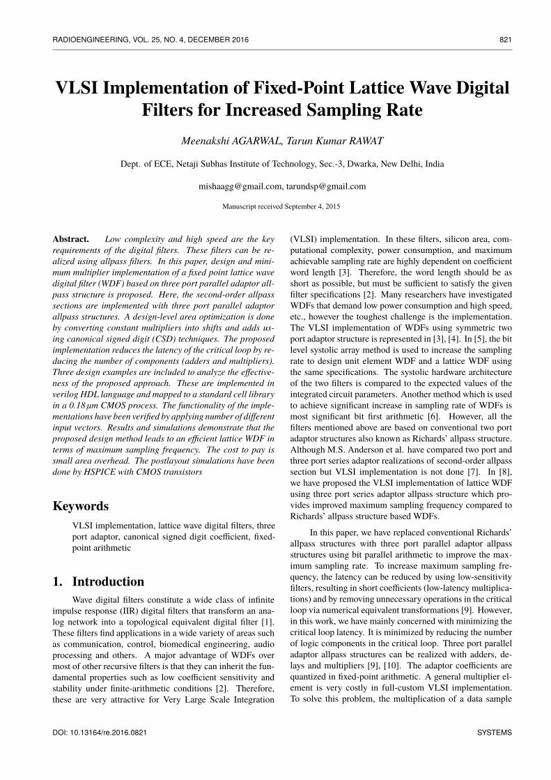
2. Lattice Wave Digital FiltersAn explicit class of wave digital filters are called lattice
wave digital filter. It is well known that the lattice WDFstructures have many attractive properties such as low co-efficient sensitivity and consequently the low accuracy re-quirements for the register word length, higher dynamicrange, higher overflow level, lower round-off noise, stabil-ity and good nonlinear properties under finite-arithmeticconditions where effects of rounding, truncation and over-flow are present [2], [10], [13]. Lattice WDF struc-tures find applications in lowpass-highpass filter, bandpass-bandstop filter, Hilbert transformers and quadrature mirrorfilters (QMF) realization [14], [15]. The resulting struc-tures are found to have minimum hardware, highly modularand less sensitive, making them suitable for signal proces-sors and VLSI implementation. The lattice WDF is repre-sented by two parallel branches, which realize allpass fil-ters. These allpass filters can be realized by using first-and/or second-order wave digital allpass sections. These
Fig. 1. Lattice wave digital filter realization of N order.
sections can be implemented using symmetric two port orthree port networks known as adaptors in lattice WDF ter-minology and delay elements [16]. The signal flow graph ofadaptor consists of multipliers and adders. The multipliersare the γ coefficients that characterize the lattice WDF. Thesignal flow graph of an N th order lattice WDF is depicted inFig. 1, where block z−1 represents the unit delay. For anyorder N there are N+1
2 stages and a maximum of N adaptors.The transfer function of a lattice WDF can be written as thesum of transfer function of two allpass branches
H (z) =H0(z) + H1(z)
2(1)
where H0(z) and H1(z) are the transfer functions of stableallpass filters of orders M and N , respectively. In case of lowpass filters, M = N − 1 or M = N + 1 so that M + N orderof overall H (z) is odd. These filters can be realized in manydifferent ways [17].
In this work, we only consider the cascade realizationof the first- and second-order allpass sections. A first-orderallpass section can be realized using Richards’ structure,where a symmetric two port adaptor and a delay elementare used [9]. The second-order allpass section can be re-alized using a cascade of two first-order Richards’ allpassstructures. A second-order allpass section is also realized us-ing a three port parallel adaptor and two delay elements [1].The detailed discussion of the first- and second-order all-pass sections is given in Sec. 3. These allpass sections arerecursive structures. Generally, recursive structures requirea smaller number of arithmetic operations per sample thantheir nonrecursive counterparts. One limitation of the re-cursive structure is the maximum sampling frequency fmaxat which a filter can operate [1]. The maximum samplingfrequency for a recursive algorithm, described by a fullyspecified signal flow graph is [18]
RADIOENGINEERING, VOL. 25, NO. 4, DECEMBER 2016 823
fmax =1
Tmin= min
{Ni
Ttot
}(2)
where Tmin is the minimum sampling time, Ttot is the totallatency of the arithmetic operations and Ni is the numberof delay elements in the directed loop i [18]. The loop(s)that determines the maximum sampling frequency is calledthe critical loop(s). The digital filters with high maximumsampling frequency are suitable candidates of low power andhigh speed applications. The reason is that if required sam-pling rate is less than the maximum sampling rate, the excessspeed can be utilized to reduce the power consumption viapower supply voltage scaling techniques [17], [18]. The areacan be minimized by clever hardware design [19]. From (2),we observe two factors that are affecting the maximum sam-pling rate. The first factor is the number of delay elements inthe critical loop and second is the total latency in the criticalloop. The maximum sampling frequency can be increasedby increasing the number of delay elements in the criticalloop or by minimizing the critical loop latency. In this work,we have mainly concerned with minimizing the critical looplatency. It is minimized by reducing the number of logiccomponents in the critical loop. It is further minimized byreducing the critical delay at logic level.
3. Realization of Allpass StructuresA lattice WDF, is realized by the two parallel allpass
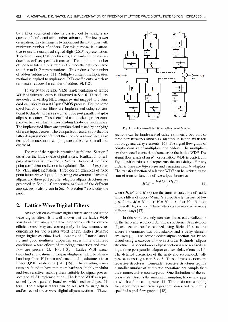
branches whose output are summed to produce the filter out-put. These allpass filters are replaced by the cascaded first-and second-order allpass sections implemented using eithersymmetric two port or three port parallel adaptor structuresand delay elements. A first-order two port adaptor has a co-efficient value (γ) which controls the response of the allpasssection. This adaptor requires a single multiplication andthree additions each. Lattice WDFs use four types of sym-metric two port adaptors as its building blocks depending onthe value of γ coefficient. The signal flow graphs of four sin-gle multiplier symmetric two port configurations are shownin Fig. 2. These adaptor coefficients γ may be guaranteedto fall into the interval −1 < γ < 1 [13]. Methods to cal-culate these coefficients from the design specifications havebeen discussed in [13]. The different adaptor structure canbe chosen depending on the value of γ coefficient as givenin Tab. 1.
In these adaptor structures, the coefficient value of theactual multiplier (α) to be implemented is always positiveand less than or equal to half, that is, 0 ≤ α ≤ 1
2 . To de-sign allpass section from these adaptor structures, one portis terminated with the delay element. Generally, the transferfunction of a first-order allpass section is given by
H (z) =t0 + z−1
1 + t0z−1 (3)
and for a second-order allpass section
H (z) =t2 + t1z−1 + z−2
1 + t1z−1 + t2z−2 (4)
Adaptor type γ range α/γ conversionType I 1
2 < γ < 1 α = 1 − γType II 0 < γ ≤ 1
2 α = γ
Type III − 12 ≤ γ < 0 α = −γ
Type IV −1 < γ < − 12 α = 1 + γ
Tab. 1. Adaptor types.
Fig. 2. Signal flow graph of four symmetric two-port adaptor.
where t0 = −γ0, t1 = (γ1 − 1)γ2 and t2 = −γ1 [13]. Thefirst- and the second-order allpass sections realized usingsymmetric two port adaptors are called as Richards’ allpassstructure. Different symmetric two port adaptor structurescan be chosen depending on the value of γ coefficient asgiven in Tab. 1. The second-order allpass sections are alsorealized using three port parallel adaptor and delays, calledas three port parallel adaptor allpass structure.
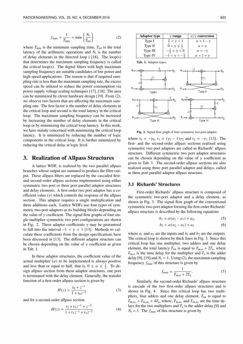
3.1 Richards’ StructuresFirst-order Richards’ allpass structure is composed of
the symmetric two-port adaptor and a delay element, asshown in Fig. 3. The signal flow graph of the conventionalsymmetric two-port adaptor forming the first-order Richards’allpass structure is described by the following equations
b1 = α(a2 − a1) + a2, (5)b2 = α(a2 − a1) + a1 (6)
where a1 and a2 are the inputs and b1 and b2 are the outputs.The critical loop is shown by thick lines in Fig. 3. Since thiscritical loop has one multiplier, two adders and one delayelement, the total latency Ttot is equal to Tm,α + 2Ta, whereTm,α is the time delay for the multiplier and Ta is the adderdelay [9], [19] and Ni = 1. Using (2), themaximum samplingfrequency fmax of this structure is given by
fmax =1
Tm,α + 2Ta. (7)
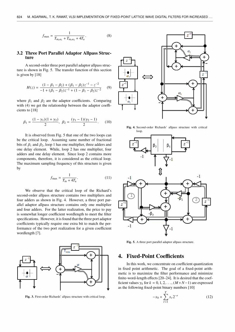
Similarly, the second-order Richards’ allpass structureis cascade of the two first-order allpass structures and isshown in Fig. 4. Since this critical loop has two multi-pliers, four adders and one delay element, Ttot is equal toTm,α1 + Tm,α2 + 4Ta, where, Tm,α1 and Tm,α2 are the time de-lays for the two multipliers and Ta is the adder delay [9] andNi = 1. The fmax of this structure is given by
824 M. AGARWAL, T. K. RAWAT, VLSI IMPLEMENTATION OF FIXED-POINT LATTICE WAVE DIGITAL FILTERS FOR INCREASED . . .
fmax =1
Tm,α1 + Tm,α2 + 4Ta. (8)
3.2 Three Port Parallel Adaptor Allpass Struc-tureA second-order three port parallel adaptor allpass struc-
ture is shown in Fig. 5. The transfer function of this sectionis given by [18]
H (z) =(1 − β1 − β2) + (β1 − β2)z−1 − z−2
−1 + (β1 − β2)z−1 + (1 − β1 − β2)z−2 (9)
where β1 and β2 are the adaptor coefficients. Comparingwith (4) we get the relationship between the adaptor coeffi-cients to [18]
β1 =(1 − γ1)(1 + γ2)
2, β2 =
(γ1 − 1)(γ2 − 1)2
. (10)
It is observed from Fig. 5 that one of the two loops canbe the critical loop. Assuming same number of fractionalbits of β1 and β2, loop 1 has one multiplier, three adders andone delay element. While, loop 2 has one multiplier, fouradders and one delay element. Since loop 2 contains morecomponents, therefore, it is considered as the critical loop.The maximum sampling frequency of this structure is givenby
fmax =1
Tm + 4Ta. (11)
We observe that the critical loop of the Richard’ssecond-order allpass structure contains two multipliers andfour adders as shown in Fig. 4. However, a three port par-allel adaptor allpass structure contains only one multiplierand four adders. For the latter realization, the price to payis somewhat longer coefficient wordlength to meet the filterspecifications. However, it is found that the three port adaptorcoefficients typically require one extra bit to match the per-formance of the two port realization for a given coefficientwordlength [7].
Fig. 3. First-order Richards’ allpass structure with critical loop.
Fig. 4. Second-order Richards’ allpass structure with criticalloop.
Fig. 5. A three port parallel adaptor allpass structure.
4. Fixed-Point CoefficientsIn this work, we concentrate on coefficient quantization
in fixed point arithmetic. The goal of a fixed-point arith-metic is to maximize the filter performance and minimizefinite-word-length effects [20–24]. It is desired that the coef-ficient values γk for k = 0, 1, 2, . . . , (M+N−1) are expressedas the following fixed-point binary numbers [10]
−x0 +
T∑r=1
xr2−r (12)
RADIOENGINEERING, VOL. 25, NO. 4, DECEMBER 2016 825
where xr for r = 0, 1, . . . , B is either 0 or 1. Here x0 isthe sign bit. For negative numbers sign bit is equal to one,whereas for non-negative numbers it is equal to zero. Thegoal is to express all the filter coefficient values in the aboveform with the minimum number of fractional bits B. Forefficient multiplier implementation in full-custom VLSI im-plementation, the multiplication of a data sample by a filtercoefficient value is carried out by using a sequence of shiftsand adds and/or subtracts. In this case, it is desired to expressthe coefficient values in the following form
R∑r=1
xr2−Pr (13)
where each xr is either 1 or −1 and the PR’s are nonnegativeintegers in the increasing order. The goal is to find all thecoefficient values with minimum number of R, the number ofpower-of-two terms and the maximum number of shifts PR
is made as small as possible [10]. For this purpose, it is at-tractive to use the canonic-signed-digit (CSD) representation.This representation has three digits, −1, 0 and +1 as opposedto the two’s-complement representation which has only twodigits, 0 and +1 [10]. The number of adders and/ or subtrac-tors required to realize a CSD coefficient is one less than thenumber of nonzero digits in this coefficient representationform [25].
5. VLSI ImplementationIn this section, VLSI implementation of lattice WDF is
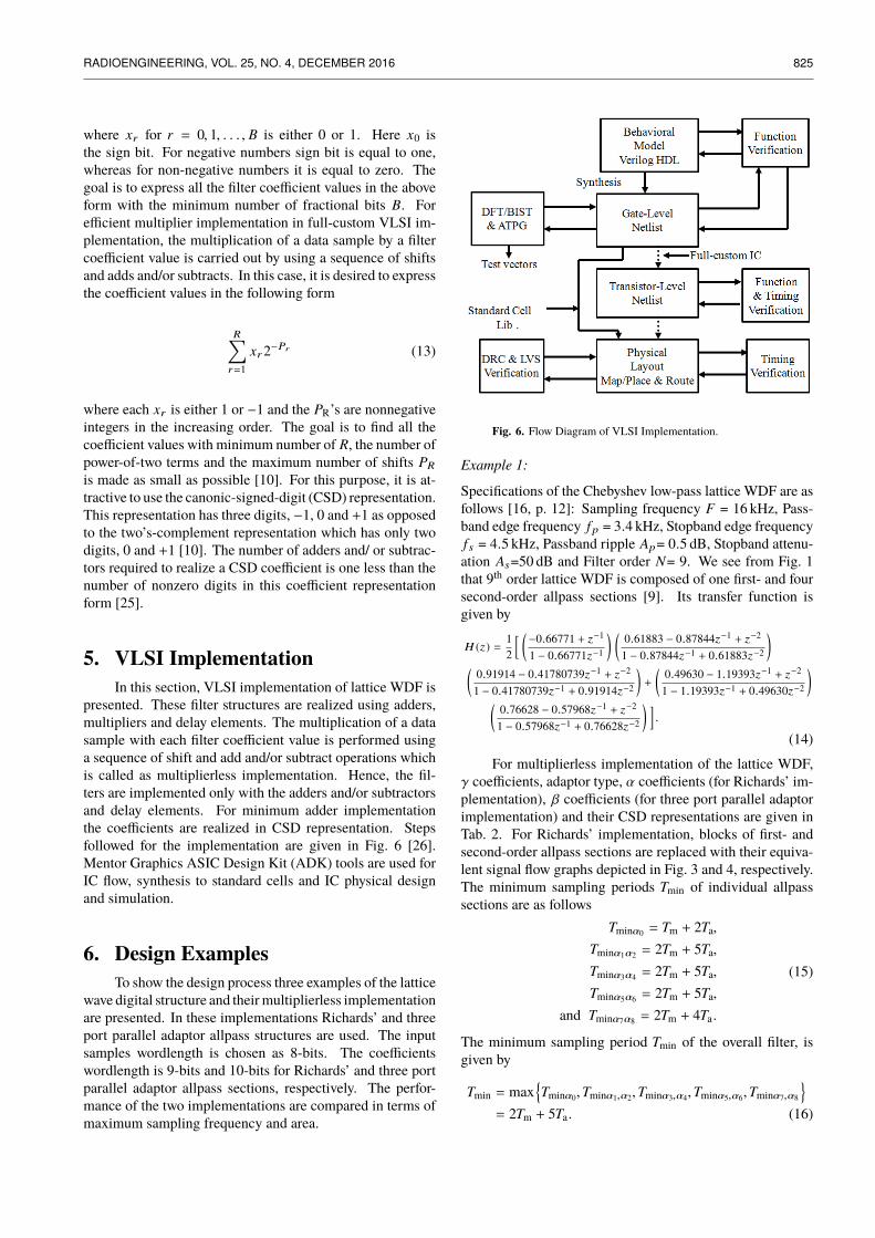
presented. These filter structures are realized using adders,multipliers and delay elements. The multiplication of a datasample with each filter coefficient value is performed usinga sequence of shift and add and/or subtract operations whichis called as multiplierless implementation. Hence, the fil-ters are implemented only with the adders and/or subtractorsand delay elements. For minimum adder implementationthe coefficients are realized in CSD representation. Stepsfollowed for the implementation are given in Fig. 6 [26].Mentor Graphics ASIC Design Kit (ADK) tools are used forIC flow, synthesis to standard cells and IC physical designand simulation.
6. Design ExamplesTo show the design process three examples of the lattice
wave digital structure and theirmultiplierless implementationare presented. In these implementations Richards’ and threeport parallel adaptor allpass structures are used. The inputsamples wordlength is chosen as 8-bits. The coefficientswordlength is 9-bits and 10-bits for Richards’ and three portparallel adaptor allpass sections, respectively. The perfor-mance of the two implementations are compared in terms ofmaximum sampling frequency and area.
Fig. 6. Flow Diagram of VLSI Implementation.
Example 1:
Specifications of the Chebyshev low-pass lattice WDF are asfollows [16, p. 12]: Sampling frequency F = 16 kHz, Pass-band edge frequency fp = 3.4 kHz, Stopband edge frequencyfs = 4.5 kHz, Passband ripple Ap= 0.5 dB, Stopband attenu-ation As=50 dB and Filter order N= 9. We see from Fig. 1that 9th order lattice WDF is composed of one first- and foursecond-order allpass sections [9]. Its transfer function isgiven by
H (z) =12
[ (−0.66771 + z−1
1 − 0.66771z−1
) (0.61883 − 0.87844z−1 + z−2
1 − 0.87844z−1 + 0.61883z−2
)(
0.91914 − 0.41780739z−1 + z−2
1 − 0.41780739z−1 + 0.91914z−2
)+
(0.49630 − 1.19393z−1 + z−2
1 − 1.19393z−1 + 0.49630z−2
)(
0.76628 − 0.57968z−1 + z−2
1 − 0.57968z−1 + 0.76628z−2
) ].
(14)
For multiplierless implementation of the lattice WDF,γ coefficients, adaptor type, α coefficients (for Richards’ im-plementation), β coefficients (for three port parallel adaptorimplementation) and their CSD representations are given inTab. 2. For Richards’ implementation, blocks of first- andsecond-order allpass sections are replaced with their equiva-lent signal flow graphs depicted in Fig. 3 and 4, respectively.The minimum sampling periods Tmin of individual allpasssections are as follows
Tminα0 = Tm + 2Ta,
Tminα1α2 = 2Tm + 5Ta,
Tminα3α4 = 2Tm + 5Ta,
Tminα5α6 = 2Tm + 5Ta,
and Tminα7α8 = 2Tm + 4Ta.
(15)
The minimum sampling period Tmin of the overall filter, isgiven by
Tmin = max{Tminα0,Tminα1,α2,Tminα3,α4,Tminα5,α6,Tminα7,α8
}
= 2Tm + 5Ta. (16)
826 M. AGARWAL, T. K. RAWAT, VLSI IMPLEMENTATION OF FIXED-POINT LATTICE WAVE DIGITAL FILTERS FOR INCREASED . . .
γi, 0 ≤ i ≤ 8 Adaptor αj, 0 ≤ j ≤ 8 αCSD βk, 1 ≤ k ≤ 8 βCSD
type0.667713527 1 0.33228647 0.01010101 − −−0.49630558 3 0.49630558 0.10000001 1.34511717 1.0101000000.797917736 1 0.202082263 0.01010100 0.1511885 0.001010010−0.618835168 4 0.381164832 0.10100010 1.24864118 1.01000000100.542641521 1 0.457358479 0.10010101 0.370194 0.101000010˘0.766286584 4 0.233713416 0.01000100 1.17298493 1.0101010000.328193215 2 0.328193215 0.01010100 0.5933016 0.101010000−0.919144204 4 0.080855796 0.00010101 1.1684758 1.0101010100.217705053 2 0.217705053 0.01001000 0.7506684 1.010000000
Tab. 2. Low-pass filter coefficients (Example 1).
The maximum sampling frequency fmax is given by
fmax =1
Tmin=
12Tm + 5Ta
. (17)
For multiplierless implementation, fmax is given by thefollowing equation
fmax = min{ 12Ta + 2Ta
,1
3Ta + 5Ta,
14Ta + 5Ta
,1
3Ta + 5Ta,
13Ta + 4Ta
}=19Ta. (18)
To implement a low-pass lattice WDF using three portparallel adaptors, blocks of second-order allpass sections arereplaced with three port parallel adaptor allpass structures,shown in Fig. 5. Although, (α0) is implemented with theRichards’ first-order allpass structure. The fmax of the overallfilter is determined by one of the critical loops of this allpasssection. The fmax in terms of Tm and Ta for each of theseallpass sections is same as given in (11). The multipliers areimplemented with a network of shift and add and/or subtractoperations using CSD coefficients. β coefficients and theirCSD equivalents are given in Tab. 2. For the multiplierlessimplementation, fmax is given by
fmax = min{
fmaxα0, fmaxβ1β2, fmaxβ3β4, fmaxβ5β6, fmaxβ7β8}
= min{16Ta,16Ta,15Ta,16Ta
}=16Ta. (19)
Comparing equations (18) and (19), we observe thatfmax is improved by approximately 49% by reducing criticaldelay. The filters are implemented in CMOS VLSI designand results are summarized in Tab. 3. Here, fmax for threeport adaptors allpass based lattice WDF is improved by 15%compared to Richards’ allpass based filter. However, the areais increased by 24%.
fmax Area (mm2) Number ofgates
Richards’ allpass 58.5 MHz 2.952 2304Three port adaptor 67.6 MHZ 3.669 2887
allpass
Tab. 4. Comparison of fmax and area of low-pass lattice WDFbased on Richards’ and three port parallel adaptor struc-tures (Example1).
Example 2:
Consider an elliptic low-pass lattice WDF with the followingspecifications [13]. F = 16 kHz, fp = 3 kHz, fs = 5 kHz, Ap
= 1.0 dB , As = 40 dB, Filter type = Chebyshev, and N=5.From Fig. 1, we observe that 5th order lattice WDF consistsof one first- and two second-order allpass sections. For theabove specifications, transfer function is given by
H (z) =12
[ (−0.6338 + z−11 − 0.6338z−1
) (0.8260 − 0.68566z−1 + z−21 − 0.68566z−1 + 0.8260z−2
)
+
(0.5372 − 1.01532z−1 + z−21 − 1.0153z−1 + 0.5372z−2
) ].
(20)
For multiplierless implementation of the lattice WDF,γ coefficients, adaptor type, α coefficients (for Richards’implementation), β coefficients (for three port parallel adap-tor implementation) and their CSD representations are givenin Tab. 4. For Richards’ structure implementation, fmax isgiven by
fmax = min{
12Ta + 2Ta
,1
4Ta + 5Ta,
13Ta + 4Ta
}
= min{14Ta,19Ta,17Ta
}=19Ta. (21)
To implement the low-pass latticeWDF using three portparallel adaptors, the fmax in terms of Tm and Ta for each ofthese allpass sections, is same as given in (11). The β coeffi-cients and their CSD equivalents are given in Tab. 4. For themultiplierless implementation, fmax is given as follows
fmax = min{
fmaxα0, fmaxβ1β2, fmaxβ3β4}
= min{14Ta,17Ta,16Ta
}=17Ta. (22)
Comparing equations (21) and (22) shows that fmax isimproved by approximately 28.5% by reducing critical loopdelay. The filters are implemented in CMOS VLSI design toverify the results and are summarized inTab. 5. Here, fmax forthree port adaptors allpass based lattice WDF is improved byapproximately 16.5% compared to Richards’ allpass basedfilter. However, the area is increased by 18%.
−
RADIOENGINEERING, VOL. 25, NO. 4, DECEMBER 2016 827
γi, 0 ≤ i ≤ 4 Adaptor αj, 0 ≤ j ≤ 4 αCSD βk, 1 ≤ k ≤ 4 βCSD
type0.6338 1 0.3662 0.10100010 − −
−0.5372 4 0.4628 0.1000101 1.2762603 1.0100101010.6605 1 0.3395 0.10101001 0.26093 0.010001010−0.8360 4 0.1740 0.01010101 1.262709 1.0100010010.3755 1 0.3755 0.10100000 0.573291 0.10010101
Tab. 3. Coefficients of low-pass WDF filter (Example 2).
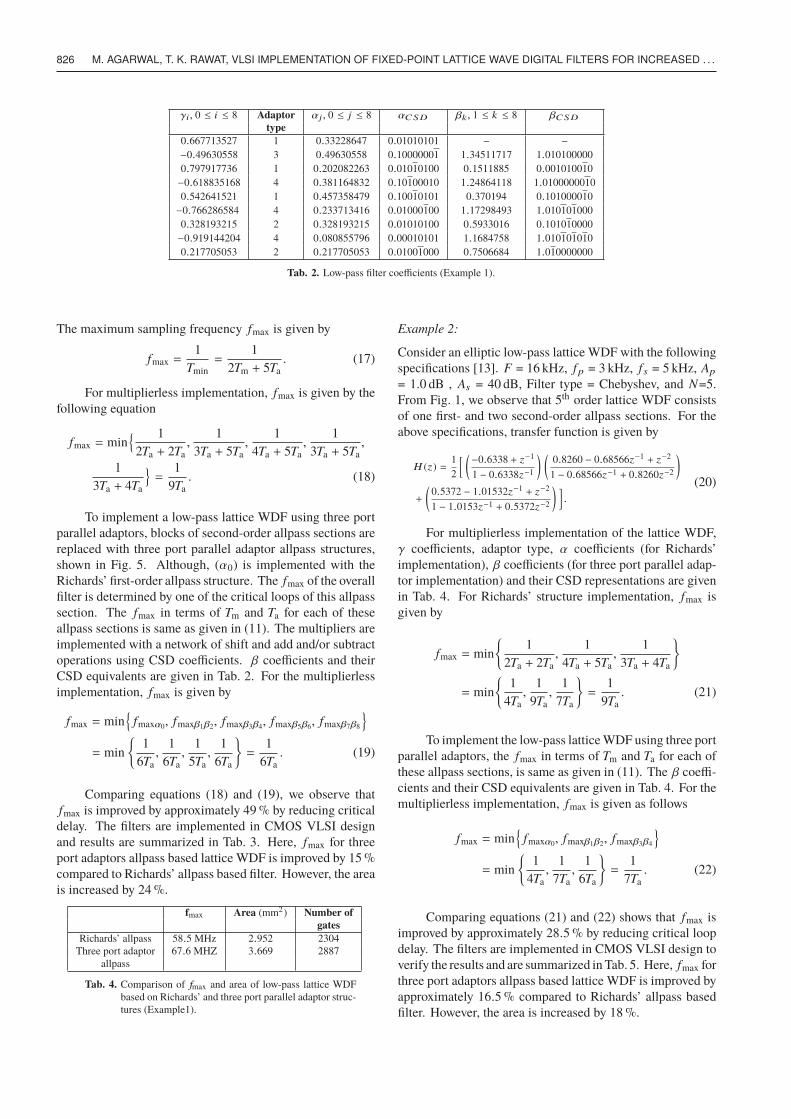
Fig. 7. Magnitude response (a), phase response (b), input signal (c), filtered output (d).
fmax Area (mm2) Number ofgates
Richards’ allpass 70.0 MHz 1.934 1476Three port adaptor 81.6 MHZ 2.285 1698
allpass
Tab. 6. Comparison of fmax and area of low-pass lattice WDF(Example 2).
Example 3:
Consider an elliptic low-pass lattice WDF with the followingspecifications [13]. F=16 kHz, fp = 3.4 kHz, fs = 4.6 kHz,Ap= 0.2 dB, As=65 dB, Filter type= Cauer, and Filter orderN= 7. From Fig. 1, we observed that the 7th order latticeWDF requires one first- and three second-order allpass sec-tions. For given filter specifications, the transfer function isobtained as
fmax Area (mm2) Number ofgates
Richards’ allpass 63.1 MHz 2.472 1865Three port adaptor 71.3 MHz 2.966 2595
allpass
Tab. 7. Comparison of fmax and area of low-pass lattice WDF(Example 3).
H (z) =12
[ (−0.5190 + z−1
1 − 0.5190z−1
) (0.66872 − 0.557752z−1 + z−2
1 − 0.55772z−1 + 0.66872z−2
)+
(0.40441 − 0.853474z−1 + z−2
1 − 0.853474z−1 + 0.40441z−2
) (0.89613 − 0.39193z−1 + z−2
1 − 0.39193z−1 + 0.89613z−2
) ].
(23)
The magnitude and phase response of the designed fil-ter are depicted in Fig. 7(a) and 7(b). When an input signalx(t) = sin(80πt) + sin(12000πt) is applied to the filter, its
γi, 0 ≤ i ≤ 6 Adaptor αj, 0 ≤ j ≤ 6 αCSD βk, 1 ≤ k ≤ 6 βCSD
type0.51290 1 0.4871 0.10000101 − −
−0.40441 3 0.40441 0.10101000 0.8337626 1.0010101010.60271 1 0.3922 0.10100100 0.2618522 0.010001010−0.66872 4 0.3313 0.1010101 1.113236 1.0010010100.33424 2 0.33424 0.10101010 0.5554835 0.100100100−0.89613 4 0.1038 0.00100101 1.14402056 1.0010010100.20669 2 0.2067 0.01010101 0.69502645 1.0101001
Tab. 5. Low-pass filter coefficients Example 3.
828 M. AGARWAL, T. K. RAWAT, VLSI IMPLEMENTATION OF FIXED-POINT LATTICE WAVE DIGITAL FILTERS FOR INCREASED . . .
output is y(t) = sin(80πt). Both x(t) and y(t) are shownin Fig. 7(c) and 7(d). The responses shown in Fig. 7 areillustrated using MATLAB tool.
For multiplierless implementation of the lattice WDF,γ coefficients, adaptor type, α coefficients (for Richards’ im-plementation), β coefficients (for three port parallel adaptorbased implementation) and their CSD representations aregiven in Tab. 6. For Richards’ implementation, fmax is givenby
fmax = min{
12Ta + 2Ta
,1
4Ta + 5Ta,
14Ta + 4Ta
,1
4Ta + 4Ta
}
= min{14Ta,19Ta,18Ta,18Ta
}=19Ta. (24)
To implement a low-pass lattice WDF using three portparallel adaptors, the fmax in terms of Tm and Ta for each ofthese allpass sections, is same as given in (11). β coefficientsand their CSD equivalents are given in Tab. 6. For multipli-erless implementation, minimum fmax of the overall filter isgiven by
fmax = min{
fmaxα0, fmaxβ1β2, fmaxβ3β4, fmaxβ5β6}
= min{14Ta,17Ta,16Ta,16Ta
}=17Ta. (25)
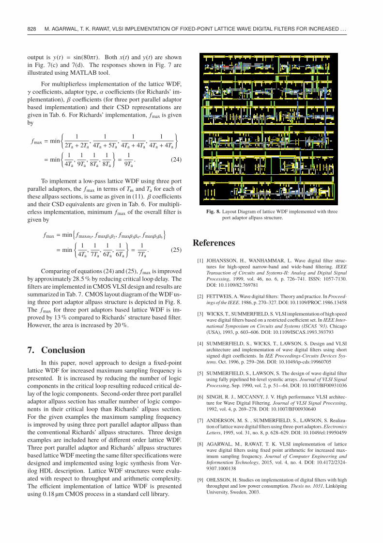
Comparing of equations (24) and (25), fmax is improvedby approximately 28.5% by reducing critical loop delay. Thefilters are implemented in CMOSVLSI design and results aresummarized in Tab. 7. CMOS layout diagram of theWDFus-ing three port adaptor allpass structure is depicted in Fig. 8.The fmax for three port adaptors based lattice WDF is im-proved by 13% compared to Richards’ structure based filter.However, the area is increased by 20%.
7. ConclusionIn this paper, novel approach to design a fixed-point
lattice WDF for increased maximum sampling frequency ispresented. It is increased by reducing the number of logiccomponents in the critical loop resulting reduced critical de-lay of the logic components. Second-order three port paralleladaptor allpass section has smaller number of logic compo-nents in their critical loop than Richards’ allpass section.For the given examples the maximum sampling frequencyis improved by using three port parallel adaptor allpass thanthe conventional Richards’ allpass structures. Three designexamples are included here of different order lattice WDF.Three port parallel adaptor and Richards’ allpass structuresbased latticeWDFmeeting the same filter specificationsweredesigned and implemented using logic synthesis from Ver-ilog HDL description. Lattice WDF structures were evalu-ated with respect to throughput and arithmetic complexity.The efficient implementation of lattice WDF is presentedusing 0.18 μm CMOS process in a standard cell library.
Fig. 8. Layout Diagram of lattice WDF implemented with threeport adaptor allpass structure.
References
[1] JOHANSSON, H., WANHAMMAR, L. Wave digital filter struc-tures for high-speed narrow-band and wide-band filtering. IEEETransaction of Circuits and Systems-II: Analog and Digital SignalProcessing, 1999, vol. 46, no. 6, p. 726–741. ISSN: 1057-7130.DOI: 10.1109/82.769781
[2] FETTWEIS, A.Wave digital filters: Theory and practice. InProceed-ings of the IEEE. 1986, p. 270–327. DOI: 10.1109/PROC.1986.13458
[3] WICKS,T., SUMMERFIELD, S.VLSI implementation of high speedwave digital filters based on a restricted coefficient set. In IEEE Inter-national Symposium on Circuits and Systems (ISCAS ’93). Chicago(USA), 1993, p. 603–606. DOI: 10.1109/ISCAS.1993.393793
[4] SUMMERFIELD, S., WICKS, T., LAWSON, S. Design and VLSIarchitecture and implementation of wave digital filters using shortsigned digit coefficients. In IEE Proceedings-Circuits Devices Sys-tems. Oct. 1996, p. 259–266. DOI: 10.1049/ip-cds:19960705
[5] SUMMERFIELD, S., LAWSON, S. The design of wave digital filterusing fully pipelined bit-level systolic arrays. Journal of VLSI SignalProcessing, Sep. 1990, vol. 2, p. 51-–64. DOI: 10.1007/BF00931036
[6] SINGH, R. J., MCCANNY, J. V. High performance VLSI architec-ture for Wave Digital Filtering. Journal of VLSI Signal Processing,1992, vol. 4, p. 269–278. DOI: 10.1007/BF00930640
[7] ANDERSON, M. S. , SUMMERFIELD, S., LAWSON, S. Realiza-tion of latticewave digital filters using three-port adaptors.ElectronicsLetters, 1995, vol. 31, no. 8, p. 628–629. DOI: 10.1049/el:19950459
[8] AGARWAL, M., RAWAT, T. K. VLSI implementation of latticewave digital filters using fixed point arithmetic for increased max-imum sampling frequency. Journal of Computer Engineering andInformention Technology, 2015, vol. 4, no. 4. DOI: 10.4172/2324-9307.1000138
[9] OHLSSON, H. Studies on implementation of digital filters with highthroughput and low power consumption. Thesis no. 1031, LinköpingUniversity, Sweden, 2003.
x(t) y(t)
RADIOENGINEERING, VOL. 25, NO. 4, DECEMBER 2016 829
[10] YLI-KAAKINEN, J., SARAMÄKI, T. A systematic algorithm for thedesign of lattice wave digital filters with short-coefficient wordlength.IEEE Transaction on Circuits and Systems-I, 2007, vol. 54, no. 8,p. 1838–1851. DOI: 10.1109/TCSI.2007.902513
[11] OHLSSON, H., GUSTAFSSON, O., JOHANSSON, H., et al. Im-plementation of bit-parallel lattice wave digital filters with increasedmaximal sample rate. In Proceedings of 8th IEEE Conference onElectronics, Circuits and Systems (ICECS), 2001, vol. 1, p. 71–74.DOI: 10.1109/ICECS.2001.957672
[12] JOHANSSON, K., GUSTAFSSON, O., WANHAMMAR, L. Mul-tiple constant multiplication for digit-serial implementation of lowpower FIR filters.WSEAS Transaction on Circuits and Systems, 2006,vol. 5, no. 7, p. 1001–1008.
[13] GAZSI, L. Explicit formulas for lattice wave digital filters. IEEETransactions on Circuits and Systems, 1985, vol. 32, no. 1, p. 68–88.DOI: 10.1109/TCS.1985.1085595
[14] AGARWAL, M., BARSAINYA, R., RAWAT, T. K. FPGA im-plementation of Hilbert transformer based on lattice wave digi-tal filters. In Proceedings of 4th IEEE Conference on Reliability,Infocom Technologies and Optimization (ICRITO). 2015, p. 1–5.DOI: 10.1109/ICRITO.2015.7359331
[15] BARSAINYA, R., AGARWAL, M., RAWAT, T. K. Multiplier-lessimplementation of quadrature mirror filter. In Proceedings of 4thIEEEConference on Reliability, Infocom Technologies and Optimiza-tion (ICRITO). 2015, p. 1–6. DOI: 10.1109/ICRITO.2015.7359328
[16] VENKAT, K. Wave Digital Filtering Using MSP430 – ApplicationReport, Texas Instruments. 25 pages. 2006.
[17] WANHAMMAR, L.DSP Integrated Circuits. NewYork (USA): Aca-demic Press, 1999.
[18] GUSTAFSSON, O., WANHAMMAR, L. Maximally fast schedul-ing of bit-serial lattice wave digital filters using three-port adaptorallpass sections. In Proceeding of Nordic Signal Processing Sympo-sium. 2000, p. 441–444.
[19] OHLSSON, H., WANHAMMAR, L. Implementation of bit-parallellattice wave digital filters. In Proceeding of Swedish System-on-ChipConference. 2001, p. 71–74.
[20] GOETTE, J. On fixed-point filter realizations. Bern University of Ap-plied Sciences, Biel/Bienne Institute of Human Centered Engineering- microLab, Feb. 2015.
[21] VOLKOVA, A., HILAIRE, T. Fixed-point implementation of latticewave digital filter: comparison and error analysis. In Proceedings ofthe 23rd European Signal Processing Conference (EUSIPCO). 2015,p. 1118–1122. DOI: 10.1109/EUSIPCO.2015.7362557
[22] YATES, R. Practical Considerations in Fixed-Point FIR Filter Im-plementations. Sep. 2010.
[23] MATHWORKS. Fixed-Point Filter Design in MATLAB(documentation). [online] Cited 2015-08-14. Available at:http://in.mathworks.com/help/dsp/ug/fixed-point-filter-design.html
[24] DOLECEK, G. J., LADDOMADA, M. An improved class ofmultiplierless decimation filters: Analysis and design. Digi-tal Signal Processing, 2013, vol. 23, no. 5, p. 1773–1782.DOI: 10.1016/j.dsp.2013.05.011
[25] Constant Multiplier Optimization to Reduce Area (MAT-LAB Examples). [Online] Cited 2015-08-20. Available at:http://www.mathworks.com/examples/matlab-hdl-coder/1311-constant-multiplier-optimization-to-reduce-area
[26] NELSON, B. Test Generation and Design for Test (MentorGraphics) Document. [Online] Cited 2016-03-10. Available at:http://www.eng.auburn.edu/ strouce/class/elec6970/NelsonBIST.pdf
About the Authors . . .
Meenakshi AGARWAL received her B.Tech degree in Elec-tronics and Telecommunication Engineering in the year 2005from CERT, UPTU University, Lucknow. She received herM.Tech, exemplary performance in 2009. She is currentlypursuing Ph. D. from Netaji Subhas Institute of Technology(NSIT), University of Delhi.
Tarun Kumar RAWAT received his M.Tech. and Ph.D.degrees, from NSIT, University of Delhi, in 2003 and 2010,respectively. Presently he is associated with NSIT, Delhi,India as Assistant Professor in the Division of Electronicsand Communication Engineering. His research interests in-clude digital signal processing, statistical signal processingand filter optimization. He has published more than 30 re-search papers in international journals and two books: Signaland System, Digital Signal Processing in Oxford UniversityPress.


