Embed Size (px)
Citation preview
11998 Morgan Kaufmann Publishers
Chapter Five
The Processor: Datapath and Control
21998 Morgan Kaufmann Publishers
• We're ready to look at an implementation of the MIPS
• Simplified to contain only:
– memory-reference instructions: lw, sw – arithmetic-logical instructions: add, sub, and, or, slt– control flow instructions: beq, j
• Generic Implementation:
– use the program counter (PC) to supply instruction address
– get the instruction from memory
– read registers
– use the instruction to decide exactly what to do
• All instructions use the ALU after reading the registers
Why? memory-reference? arithmetic? control flow?
The Processor: Datapath & Control
31998 Morgan Kaufmann Publishers
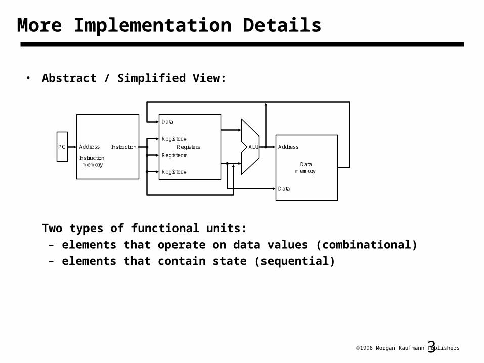
• Abstract / Simplified View:
Two types of functional units:– elements that operate on data values (combinational)– elements that contain state (sequential)
More Implementation Details
Registers
Register #
Data
Register #
Datamemory
Address
Data
Register #
PC Instruction ALU
Instructionmemory
Address
41998 Morgan Kaufmann Publishers
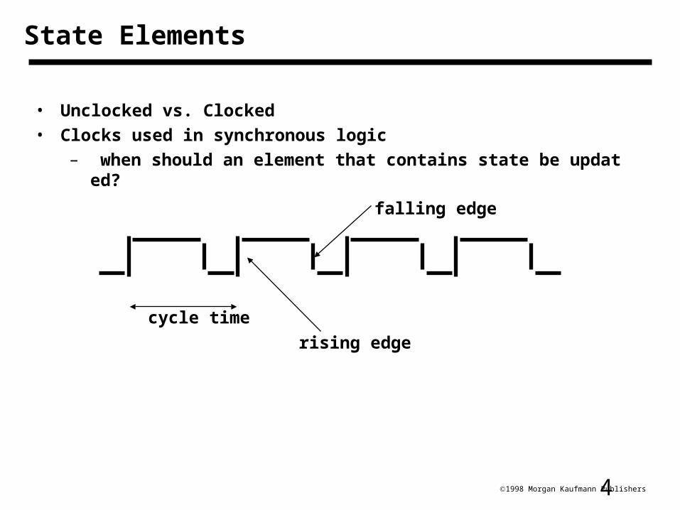
• Unclocked vs. Clocked
• Clocks used in synchronous logic
– when should an element that contains state be updated?
cycle time
rising edge
falling edge
State Elements
51998 Morgan Kaufmann Publishers
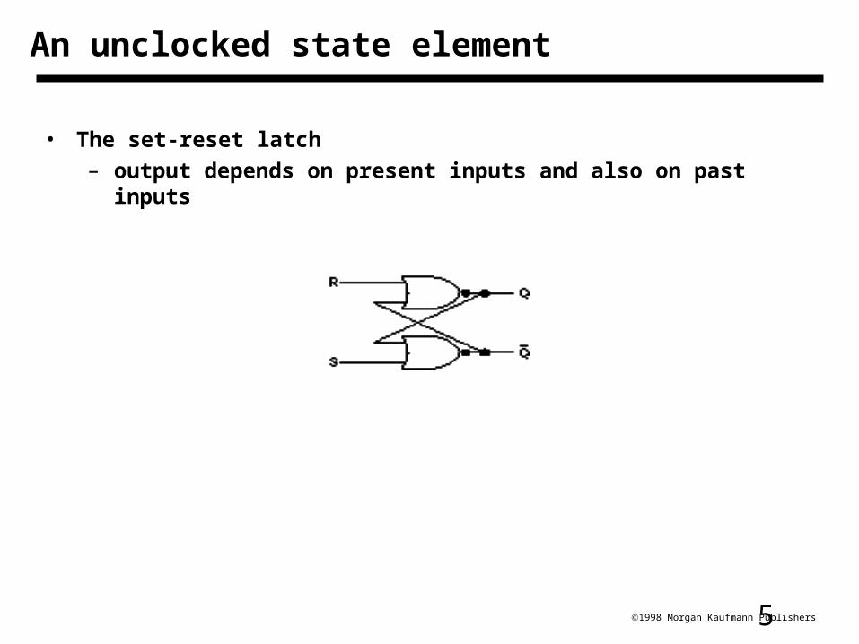
• The set-reset latch
– output depends on present inputs and also on past inputs
An unclocked state element
61998 Morgan Kaufmann Publishers
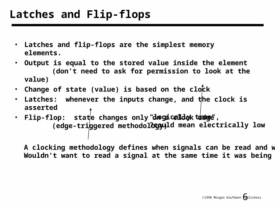
• Latches and flip-flops are the simplest memory elements.
• Output is equal to the stored value inside the element(don't need to ask for permission to look at the value)
• Change of state (value) is based on the clock
• Latches: whenever the inputs change, and the clock is asserted
• Flip-flop: state changes only on a clock edge(edge-triggered methodology)
"logically true", ?could mean electrically low
A clocking methodology defines when signals can be read and writtenWouldn't want to read a signal at the same time it was being written
Latches and Flip-flops
71998 Morgan Kaufmann Publishers
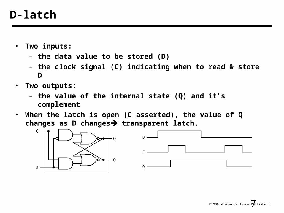
• Two inputs:
– the data value to be stored (D)
– the clock signal (C) indicating when to read & store D
• Two outputs:
– the value of the internal state (Q) and it's complement
• When the latch is open (C asserted), the value of Q changes as D changes transparent latch.
D-latch
Q
C
D
_Q
D
C
Q
81998 Morgan Kaufmann Publishers
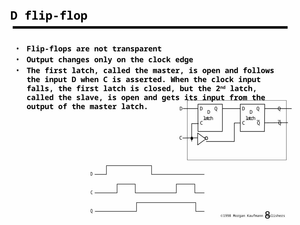
D flip-flop
• Flip-flops are not transparent
• Output changes only on the clock edge
• The first latch, called the master, is open and follows the input D when C is asserted. When the clock input falls, the first latch is closed, but the 2nd latch, called the slave, is open and gets its input from the output of the master latch.
_Q
Q
_Q
Dlatch
D
C
Dlatch
DD
C
C
D
C
Q
91998 Morgan Kaufmann Publishers
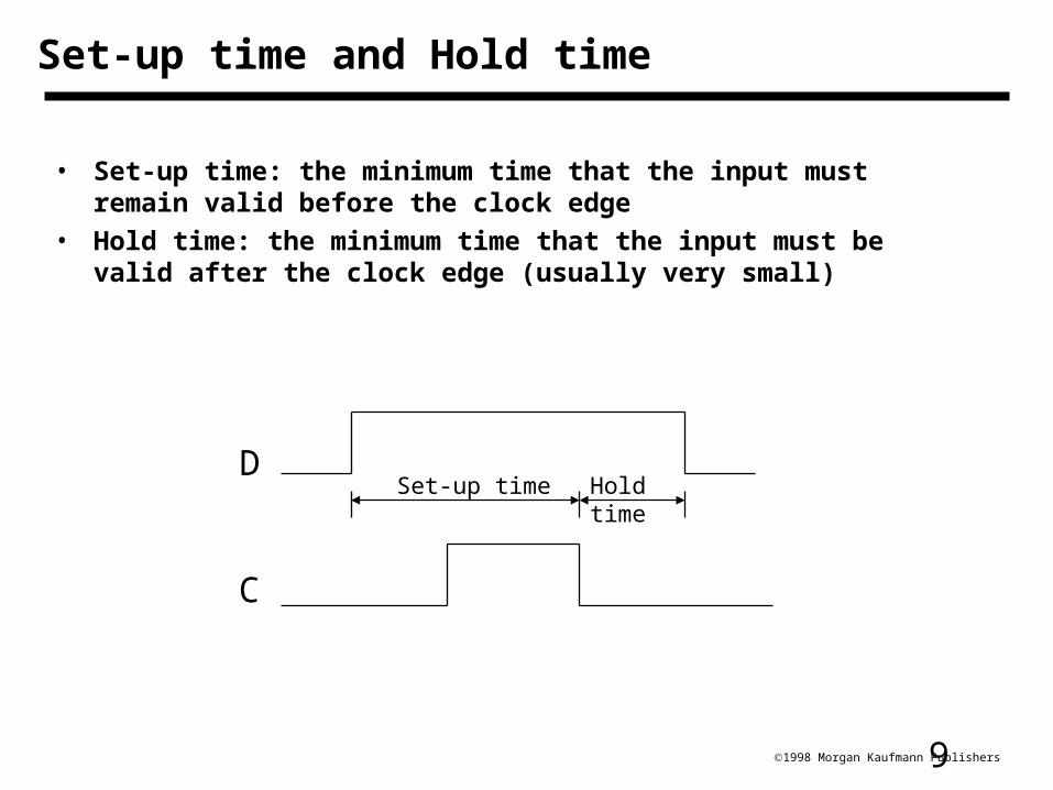
Set-up time and Hold time
• Set-up time: the minimum time that the input must remain valid before the clock edge
• Hold time: the minimum time that the input must be valid after the clock edge (usually very small)
D
C
Set-up time Hold time
101998 Morgan Kaufmann Publishers
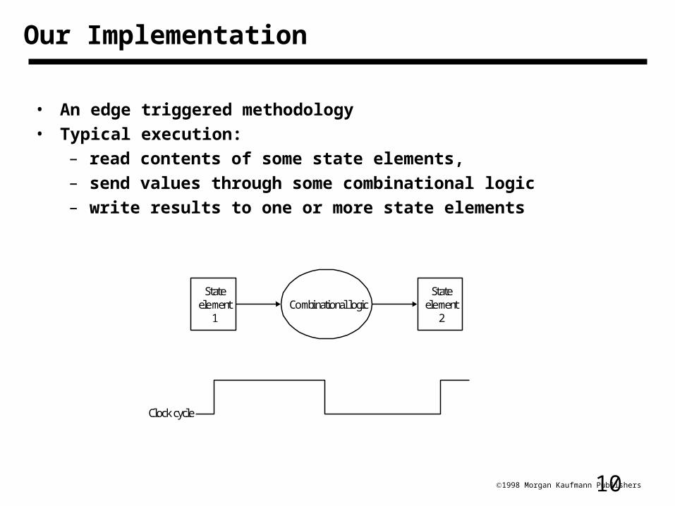
Our Implementation
• An edge triggered methodology
• Typical execution:
– read contents of some state elements,
– send values through some combinational logic
– write results to one or more state elements
Clock cycle
Stateelement
1Combinational logic
Stateelement
2
111998 Morgan Kaufmann Publishers
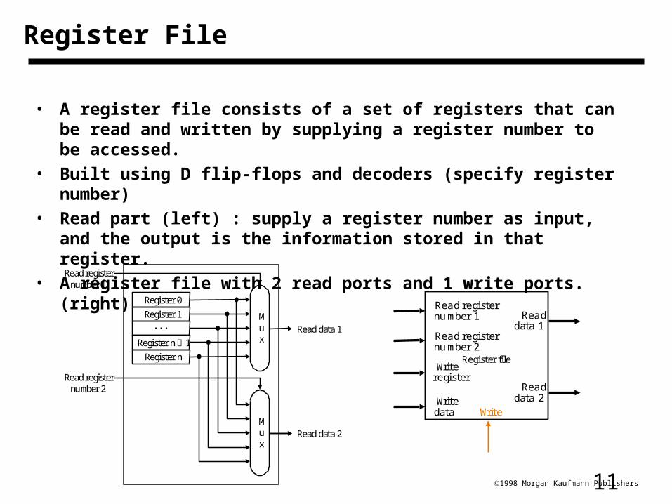
• A register file consists of a set of registers that can be read and written by supplying a register number to be accessed.
• Built using D flip-flops and decoders (specify register number)
• Read part (left) : supply a register number as input, and the output is the information stored in that register.
• A register file with 2 read ports and 1 write ports. (right)
Register File
Mux
Register 0
Register 1
Register n 1
Register n
Mux
Read data 1
Read data 2
Read registernumber 1
Read registernumber 2
Read registernumber 1 Read
data 1
Readdata 2
Read registernumber 2
Register fileWriteregister
Writedata Write
121998 Morgan Kaufmann Publishers
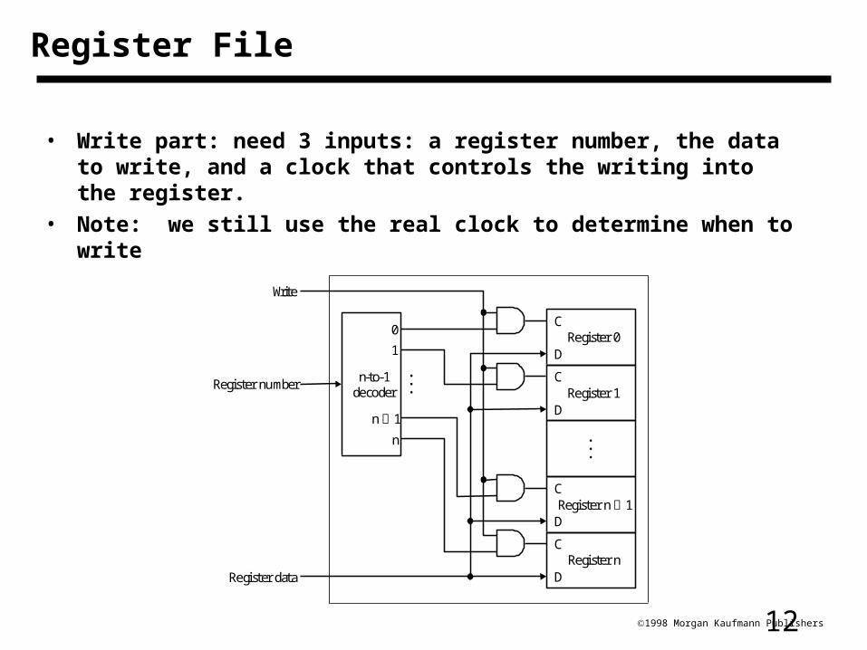
Register File
• Write part: need 3 inputs: a register number, the data to write, and a clock that controls the writing into the register.
• Note: we still use the real clock to determine when to write
n-to-1decoder
Register 0
Register 1
Register n 1C
C
D
DRegister n
C
C
D
D
Register number
Write
Register data
0
1
n 1
n
131998 Morgan Kaufmann Publishers
Simple Implementation
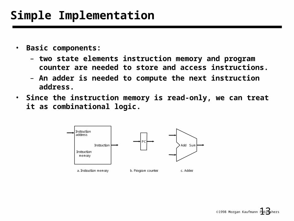
• Basic components:
– two state elements instruction memory and program counter are needed to store and access instructions.
– An adder is needed to compute the next instruction address.
• Since the instruction memory is read-only, we can treat it as combinational logic.
PC
Instructionmemory
Instructionaddress
Instruction
a. Instruction memory b. Program counter
Add Sum
c. Adder
141998 Morgan Kaufmann Publishers
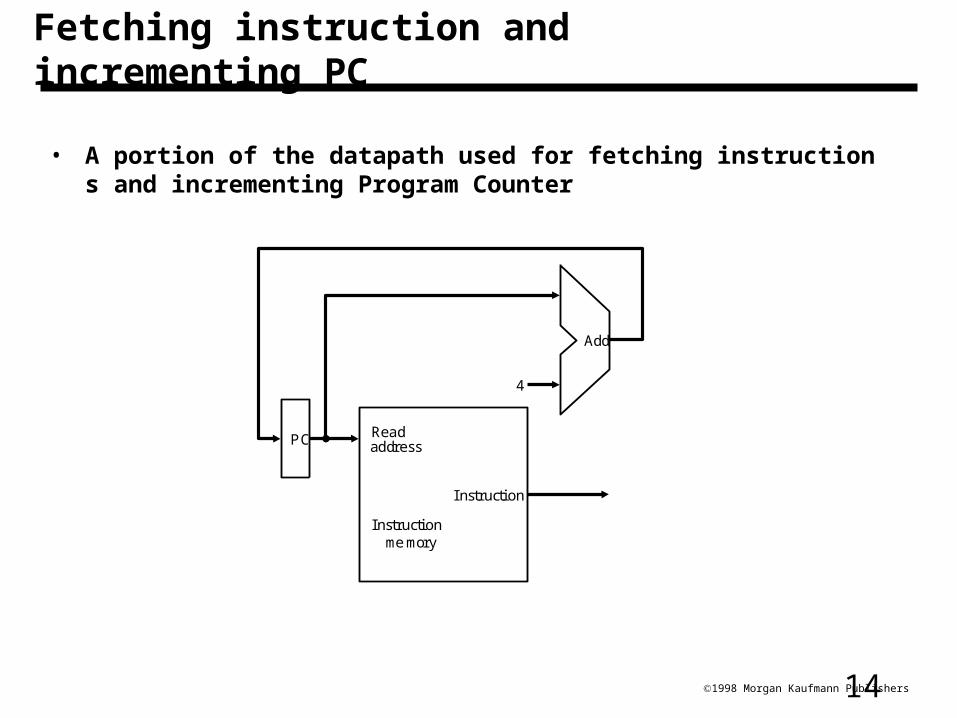
Fetching instruction and incrementing PC
• A portion of the datapath used for fetching instructions and incrementing Program Counter
PC
Instructionmemory
Readaddress
Instruction
4
Add
151998 Morgan Kaufmann Publishers
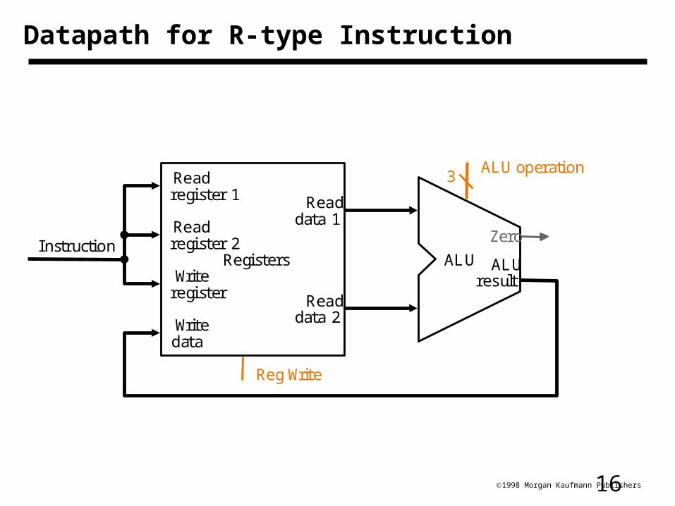
R-Format ALU operations
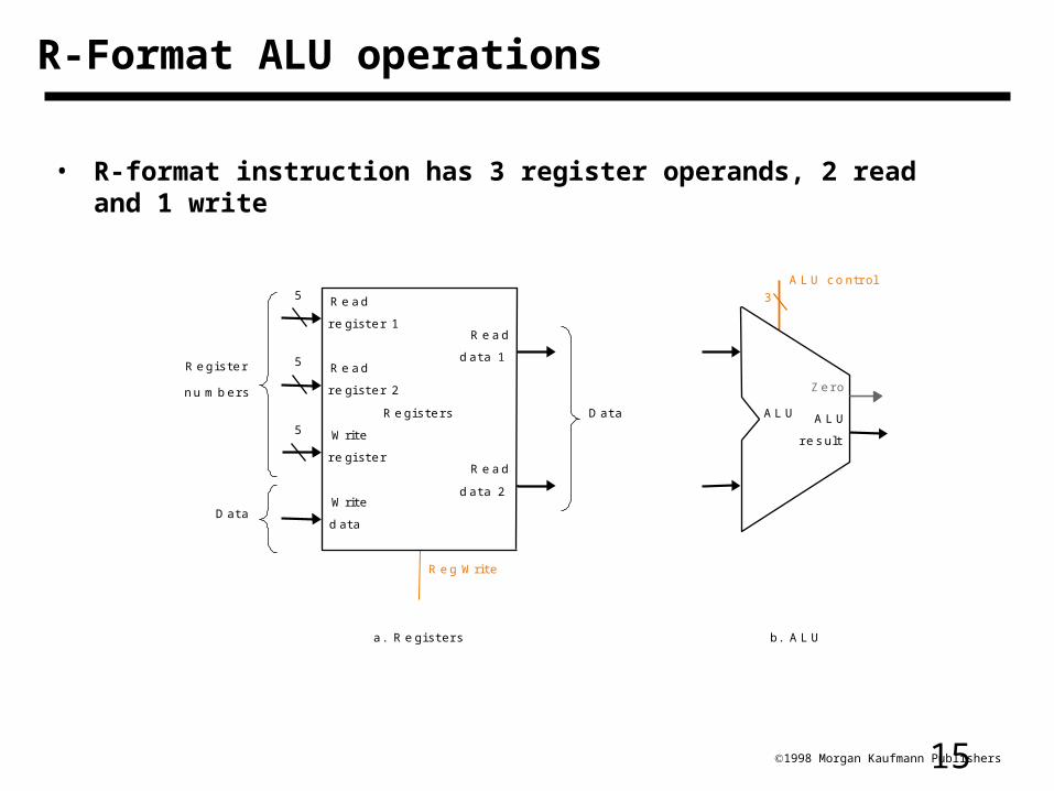
• R-format instruction has 3 register operands, 2 read and 1 write
A L U c o n t r o l
R e g W r i te
R e g is te r s
W r ite
r e g i s t e r
R e a d
d a t a 1
R e a d
d a t a 2
R e a d
r e g i s t e r 1
R e a d
r e g i s t e r 2
W r ite
d a ta
A L U
r e s u lt
A L U
D a t a
D a t a
R e g is te r
n u m b e r s
a . R e g is t e r s b . A L U
Z e r o
5
5
5 3
161998 Morgan Kaufmann Publishers
Datapath for R-type Instruction
InstructionRegisters
Writeregister
Readdata 1
Readdata 2
Readregister 1
Readregister 2
Writedata
ALUresult
ALU
Zero
RegWrite
ALU operation3
171998 Morgan Kaufmann Publishers
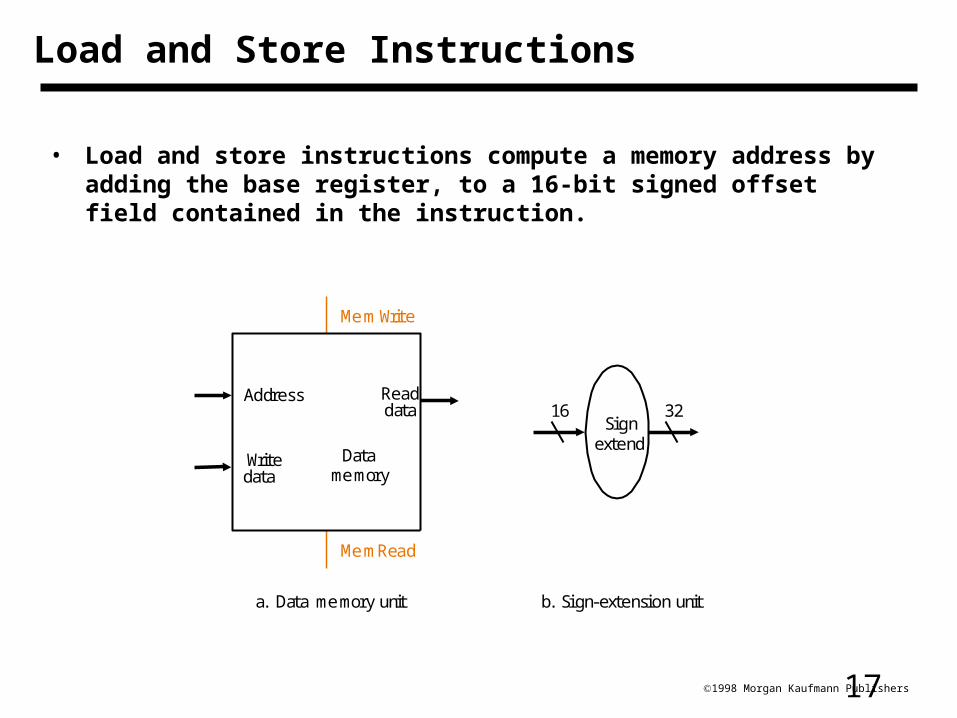
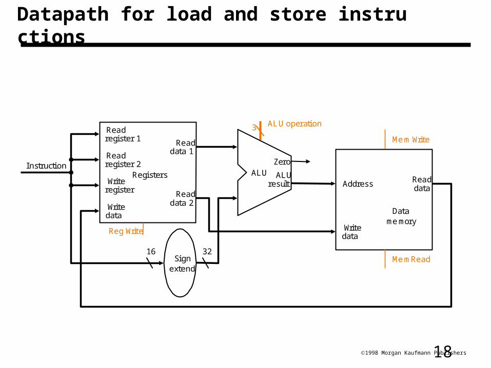
Load and Store Instructions
• Load and store instructions compute a memory address by adding the base register, to a 16-bit signed offset field contained in the instruction.
16 32Sign
extend
b. Sign-extension unit
MemRead
MemWrite
Datamemory
Writedata
Readdata
a. Data memory unit
Address
181998 Morgan Kaufmann Publishers
Datapath for load and store instructions
Instruction
16 32
RegistersWriteregister
Readdata 1
Readdata 2
Readregister 1
Readregister 2
Datamemory
Writedata
Readdata
Writedata
Signextend
ALUresult
ZeroALU
Address
MemRead
MemWrite
RegWrite
ALU operation3
191998 Morgan Kaufmann Publishers
J-type Instruction
• Branch datapath
– Needs to compute the branch target address • PC+4 is the address of the next instruction
• Offset field is left-shifted two bits to make a world offset.– Needs to compare register contents
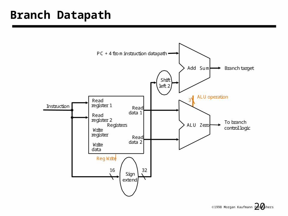
201998 Morgan Kaufmann Publishers
Branch Datapath
16 32Sign
extend
ZeroALU
Sum
Shiftleft 2
To branchcontrol logic
Branch target
PC + 4 from instruction datapath
Instruction
Add
RegistersWriteregister
Readdata 1
Readdata 2
Readregister 1
Readregister 2
Writedata
RegWrite
ALU operation3
211998 Morgan Kaufmann Publishers
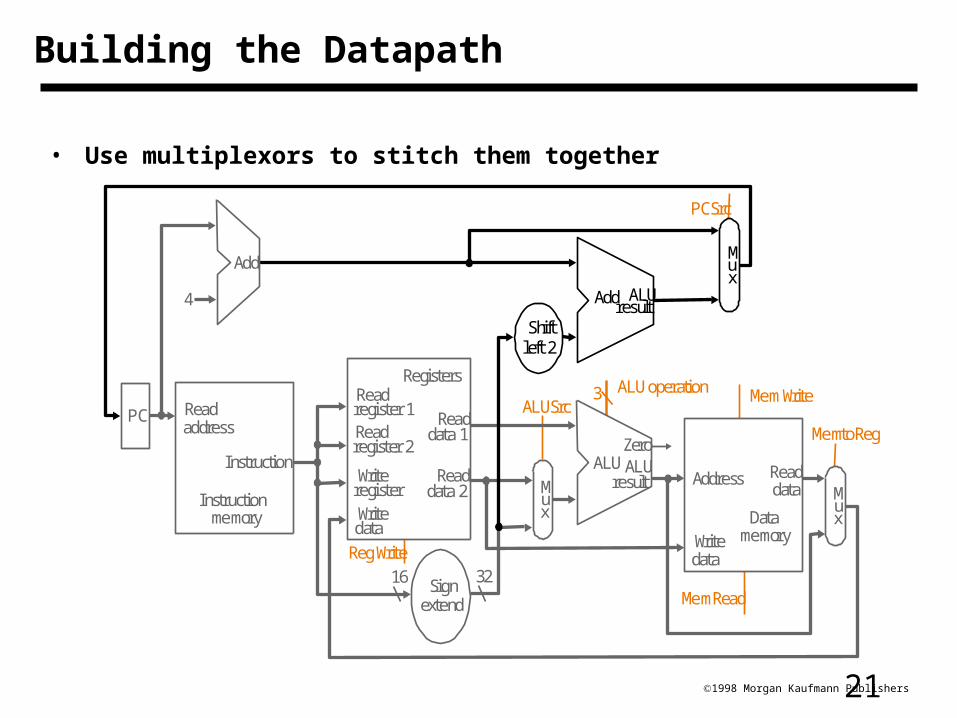
Building the Datapath
• Use multiplexors to stitch them together
PC
Instructionmemory
Readaddress
Instruction
16 32
Add ALUresult
Mux
Registers
WriteregisterWritedata
Readdata 1
Readdata 2
Readregister 1Readregister 2
Shiftleft 2
4
Mux
ALU operation3
RegWrite
MemRead
MemWrite
PCSrc
ALUSrc
MemtoReg
ALUresult
ZeroALU
Datamemory
Address
Writedata
Readdata M
ux
Signextend
Add