Embed Size (px)
Citation preview
NJU7512VT
Ver.2018-03-19 - 1 -
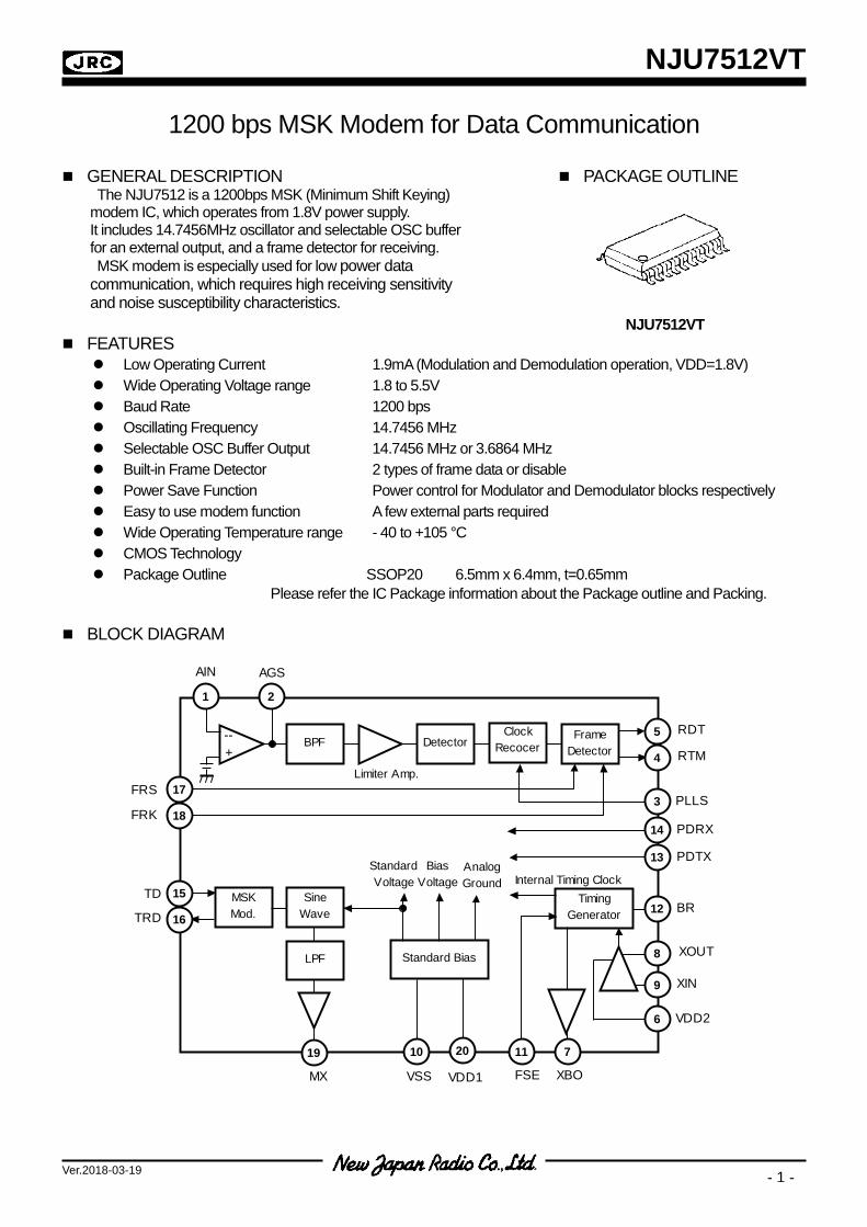
1200 bps MSK Modem for Data Communication GENERAL DESCRIPTION PACKAGE OUTLINE
The NJU7512 is a 1200bps MSK (Minimum Shift Keying) modem IC, which operates from 1.8V power supply. It includes 14.7456MHz oscillator and selectable OSC buffer for an external output, and a frame detector for receiving. MSK modem is especially used for low power data communication, which requires high receiving sensitivity and noise susceptibility characteristics.
FEATURES
Low Operating Current 1.9mA (Modulation and Demodulation operation, VDD=1.8V) Wide Operating Voltage range 1.8 to 5.5V Baud Rate 1200 bps Oscillating Frequency 14.7456 MHz Selectable OSC Buffer Output 14.7456 MHz or 3.6864 MHz Built-in Frame Detector 2 types of frame data or disable Power Save Function Power control for Modulator and Demodulator blocks respectively Easy to use modem function A few external parts required Wide Operating Temperature range - 40 to +105 °C CMOS Technology Package Outline SSOP20 6.5mm x 6.4mm, t=0.65mm
Please refer the IC Package information about the Package outline and Packing.
BLOCK DIAGRAM
NJU7512VT
DetectorClock
Recocery
BPF FrameDetector
MSKMod.
Standard Bias
TimingGenerator
Limiter Amp.
--+
StandardVoltage
BiasVoltage
AnalogGround Internal Timing Clock
SineWave
LPF
XBOFSEVDD1VSSMX
7112019 10
PLLS
PDRX
PDTX
BR
XOUT
XIN
VDD2
3
14
12
13
8
9
6
RDT
RTM
5
4
AIN AGS
1 2
TRD
TD
FRK
FRS
16
15
18
17
NJU7512VT
Ver.2018-03-19 - 2 -
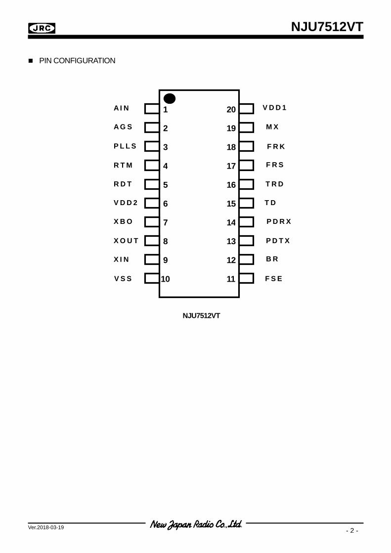
PIN CONFIGURATION
2
3
4
5
6
7
8
9
10
1
11
12
13
14
15
16
17
18
19
20A I N
A G S
P L L S
R T M
R D T
V D D 2
X B O
X O U T
X I N
V S S
V D D 1
M X
F R K
F R S
T R D
T D
P D R X
P D T X
B R
F S E
NJU7512VT
NJU7512VT
Ver.2018-03-19 - 3 -
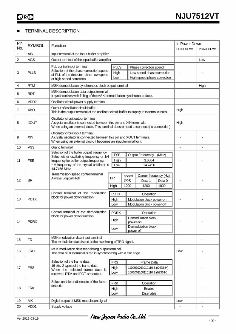
TERMINAL DESCRIPTION
Pin No. SYMBOL Function In Power Down
PDTX = Low PDRX = Low 1 AIN Input terminal of the Input buffer amplifier - - 2 AGS Output terminal of the input buffer amplifier - Low
3 PLLS PLLS Phase correction speed High Low-speed phase correction Low High-speed phase correction
PLL control input terminal Selection of the phase correction speed of PLL of the detector, either low-speed or high-speed correction.
- -
4 RTM MSK demodulation synchronous clock output terminal - High
5 RDT MSK demodulation data output terminal It synchronizes with falling of the MSK demodulation synchronous clock. -
6 VDD2 Oscillator circuit power supply terminal -
7 XBO Output of oscillator circuit buffer This is the output terminal of the oscillator circuit buffer to supply to external circuits. High
8 XOUT Oscillator circuit output terminal A crystal oscillator is connected between this pin and XIN terminals. When using an external clock, This terminal doesn't need to connect (no connection).
High
9 XIN Oscillator circuit input terminal A crystal oscillator is connected between this pin and XOUT terminals. When using an external clock, it becomes an input terminal for it.
- -
10 VSS Grand terminal - -
11 FSE FSE Output Frequency (MHz) High 3.6864 Low 14.7456
Selection of the buffer output frequency Select either oscillating frequency or 1/4 frequency for buffer output frequency. * A frequency of the crystal oscillator is 14.7456 MHz.
- -
12 BR BR speed (bps)
Career frequency (Hz) Data 1 Data 0
High 1200 1200 1800
Transmission-speed control terminal Always Logical High - -
13 PDTX
Control terminal of the modulation block for power down function.
PDTX Operation High Modulation block power-on Low Modulation block power-off
- -
14 PDRX
PDRX Operation
High Demodulation block power-on
Low Demodulation block power-off
Control terminal of the demodulation block for power down function. - -
15 TD MSK modulation data input terminal The modulation data is red at the rise timing of TRD signal. - -
16 TRD MSK modulation data read-timing output terminal The data of TD terminal is red in synchronizing with a rise edge. Low -
17 FRS
Selection of the frame data FRS Frame Data High 1100010011010110 B (C4D6 H) Low 1001001100110110 B (9336 H)
16 bits, 2 types of the frame data When the selected frame data is received, RTM and RDT are output.
- -
18 FRK FRK Operation High Enable Low Disenable
Select enable or disenable of the flame detection - -
19 MX Digital output of MSK modulation signal Low - 20 VDD1 Supply voltage - -
NJU7512VT
Ver.2018-03-19 - 4 -
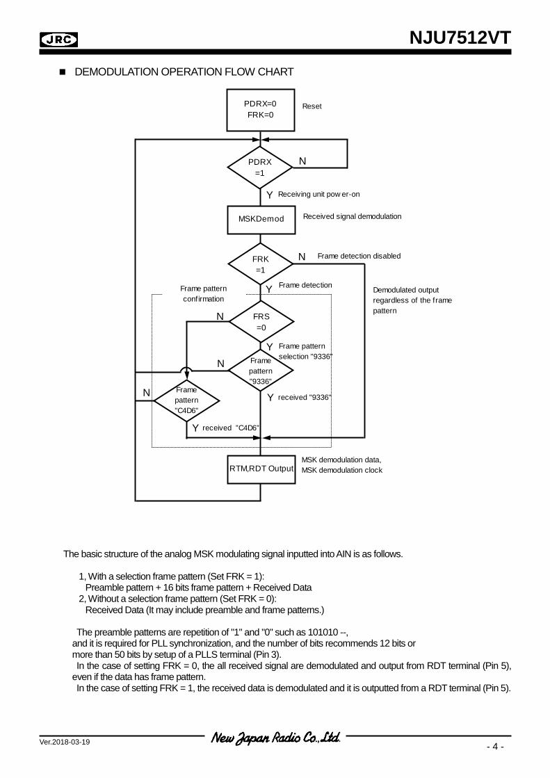
DEMODULATION OPERATION FLOW CHART The basic structure of the analog MSK modulating signal inputted into AIN is as follows.
1, With a selection frame pattern (Set FRK = 1): Preamble pattern + 16 bits frame pattern + Received Data
2, Without a selection frame pattern (Set FRK = 0): Received Data (It may include preamble and frame patterns.)
The preamble patterns are repetition of "1" and "0" such as 101010 --, and it is required for PLL synchronization, and the number of bits recommends 12 bits or more than 50 bits by setup of a PLLS terminal (Pin 3). In the case of setting FRK = 0, the all received signal are demodulated and output from RDT terminal (Pin 5), even if the data has frame pattern. In the case of setting FRK = 1, the received data is demodulated and it is outputted from a RDT terminal (Pin 5).
PDRX=0FRK=0
PDRX=1
MSKDemod
FRK=1
Reset
Receiving unit pow er-on
Received signal demodulation
Frame patternselection "9336"
RTM,RDT Output
Frame detection
MSK demodulation data,MSK demodulation clock
FRS=0
received "9336"
Y
Y
Y
Y
Y
N
N
N
N
Framepattern"9336"
Framepattern"C4D6"
N
Frame detection disabled
Demodulated outputregardless of the framepattern
Frame patternconfirmation
received ”C4D6”
NJU7512VT
Ver.2018-03-19 - 5 -
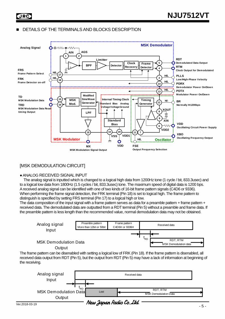
DETAILS OF THE TERMINALS AND BLOCKS DESCRIPTION [MSK DEMODULATION CIRCUIT] ● ANALOG RECEIVED SIGNAL INPUT The analog signal is inputted which is changed to a logical high data from 1200Hz tone (1 cycle / bit, 833.3usec) and to a logical low data from 1800Hz (1.5 cycles / bit, 833.3usec) tone. The maximum speed of digital data is 1200 bps. A received analog signal can be identified with one of two kinds of 16-bit frame pattern signals (C4D6 or 9336). When performing the frame signal detection, the FRK terminal (Pin 18) is set to logical high. The frame pattern to distinguish is specified by setting FRS terminal (Pin 17) to a logical high or low. The data composition of the input signal with a frame pattern serves as data for a preamble pattern + frame pattern + received data. The demodulated data are outputted from a RDT terminal (Pin 5) without a preamble and frame data. If the preamble pattern is less length than the recommended value, normal demodulation data may not be obtained. The frame pattern can be disenabled with setting a logical low of FRK (Pin 18). If the frame pattern is disenabled, all received data output from RDT (Pin 5), but the output from RDT (Pin 5) may have a lack of information at beginning of the receiving.
DetectorClock
RecoceryBPF FrameDetector
MSKMod.
TimingGenerator
5
4
3
14
12
13
8
9
71120
6
19 10
16
15
18
17
1 2Limitter
XOUT
XIN
VDD1VSS
AIN AGS
--+
BiasVoltage
AnalogGround
VDDMXMSK Modulation Signal Output
MSK Modulator
MSK Demodulator
Oscillator
Internal Timing ClockModified
SineWaveGenerator
LPF
H/L
H/L
H/L
H/-
H/L
H/L
H/L
StandardVoltage
Analog Signal
FRKFrame Detector on-off
FRSFrame Pattern Select
TDMSK Modulation DataInputTRDMSK Modulation Data Read-timing Output
RDTDemodulated Data OutputRTMClock Output for DemodulatedDataPLLSLow /High-Phase Velocity
PDTXModulator Pow er On/Dow n
PDRXDemodulator Pow er On/Dow n
BRNormally H:1200bps
StandardBias
VDD2
VDDOscillating Circuit Pow er Supply
XBOOscillating Frequency Output
FSEOutput Frequency Selection
Preamble patternMore than 12bit or 50bit
Frame patternC4D6H or 9336H
Received data
tRD RDT, RTMMSK Demodulation data
Analog signal Input
MSK Demodulation Data Output
Received data
RDT, RTMMSK Demodulation Data
Analog signal Input
MSK Demodulation Data Output
tRDLost
NJU7512VT
Ver.2018-03-19 - 6 -
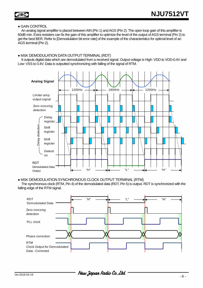
● GAIN CONTROL An analog signal amplifier is placed between AIN (Pin 1) and AGS (Pin 2). The open loop gain of this amplifier is 60dB min. Extra resisters can fix the gain of this amplifier to optimize the level of the output of AGS terminal (Pin 2) to get the best BER. Refer to [Demodulation bit error rate] of the example of the characteristics for optimal level of an AGS terminal (Pin 2). ● MSK DEMODULATION DATA OUTPUT TERMINAL (RDT) It outputs digital data which are demodulated from a received signal. Output voltage is High: VDD to VDD-0.4V and Low: VSS to 0.4V. Data is outputted synchronizing with falling of the signal of RTM. ● MSK DEMODULATION SYNCHRONOUS CLOCK OUTPUT TERMINAL (RTM) The synchronous clock (RTM, Pin 4) of the demodulated data (RDT, Pin 5) is output. RDT is synchronized with the falling edge of the RTM signal.
1200Hz 1800Hz 1200Hz
"H" "H""L"
Limiter amp.output signal
Zero crossingdetection
Delayregister
Shiftregister
Shiftregister
Detection
RDTDemodulated DataOutput
Del
ay d
etec
tion
Analog Signal
RDTDemodulated Data
Zero crossingdetection
PLL clock
RTMClock Output for DemodulatedData : Corrected
Phase correction
"H" "H""L"
NJU7512VT
Ver.2018-03-19 - 7 -
● CONTROL TERMINAL (FRS, FRK, PLLS, PDRX) 1. SELECTION OF FRAME PATTERN (FRS) One from two kinds of 16-bit frame patterns is chosen.
2. SELECTION OF FRAME DETECTION (FRK) Enabled the frame detection or disabled is chosen. When not using the frame detection, all received analog signals serve as data for demodulation. 3. SELECTION OF PHASE CORRECTION SPEED OF CLOCK REPRODUCTION (PLLS) It is a terminal which controls the pull-in bits of PLL. In order to make a synchronous clock, phase correction is applied to the internal clock, but the maximum phase correction angle is 3.75 degrees in slow mode, and is 30 degrees in fast mode. The length of the preamble pattern (repetition of "1" and "0", such as 101010--) is recommended to 50 bits and more for the slow mode, and to 12 bits and more for the fast mode. 4. MSK demodulating circuit unit power-on / power down selection (PDRX) The MSK demodulation circuit becomes operational mode in PDRX power-on function, and becomes non-operational mode in the power down function. Moreover, the frame detection circuit is reset by power down. [IMPORTANT] When the state of a FRK terminal (Pin 18) and a FRS terminal (Pin 17) is changed or after power supplied, please once choose a power down to prevent any malfunction.
FRS Selection frame pattern High 1100010011010110 B (C4D6 H) Low 1001001100110110 B (9336 H)
FRK Operation High Frame detection function enabled Low Frame detection function disabled
PLLS Phase correction speed High Low-speed phase correction Low High rank phase correction
PDRX Operation High Demodulation block power-on Low Demodulation block power-off
NJU7512VT
Ver.2018-03-19 - 8 -
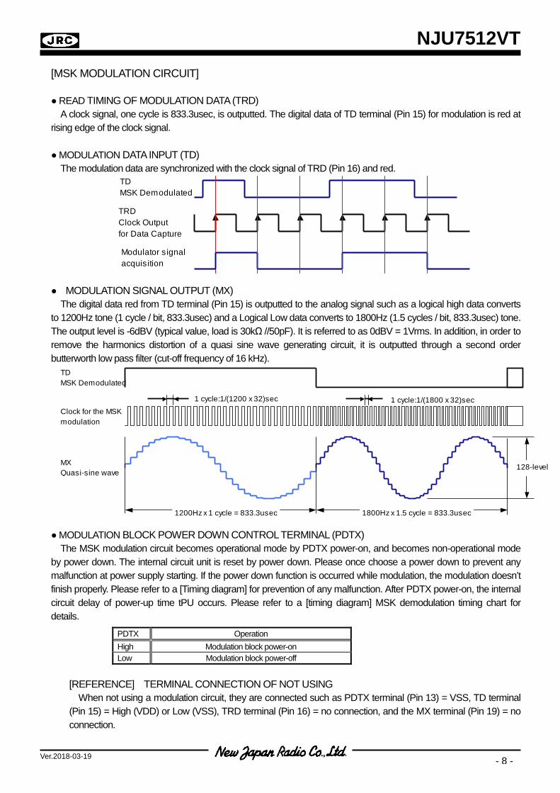
[MSK MODULATION CIRCUIT] ● READ TIMING OF MODULATION DATA (TRD) A clock signal, one cycle is 833.3usec, is outputted. The digital data of TD terminal (Pin 15) for modulation is red at rising edge of the clock signal. ● MODULATION DATA INPUT (TD) The modulation data are synchronized with the clock signal of TRD (Pin 16) and red. ● MODULATION SIGNAL OUTPUT (MX) The digital data red from TD terminal (Pin 15) is outputted to the analog signal such as a logical high data converts to 1200Hz tone (1 cycle / bit, 833.3usec) and a Logical Low data converts to 1800Hz (1.5 cycles / bit, 833.3usec) tone. The output level is -6dBV (typical value, load is 30kΩ //50pF). It is referred to as 0dBV = 1Vrms. In addition, in order to remove the harmonics distortion of a quasi sine wave generating circuit, it is outputted through a second order butterworth low pass filter (cut-off frequency of 16 kHz). ● MODULATION BLOCK POWER DOWN CONTROL TERMINAL (PDTX) The MSK modulation circuit becomes operational mode by PDTX power-on, and becomes non-operational mode by power down. The internal circuit unit is reset by power down. Please once choose a power down to prevent any malfunction at power supply starting. If the power down function is occurred while modulation, the modulation doesn’t finish properly. Please refer to a [Timing diagram] for prevention of any malfunction. After PDTX power-on, the internal circuit delay of power-up time tPU occurs. Please refer to a [timing diagram] MSK demodulation timing chart for details.
[REFERENCE] TERMINAL CONNECTION OF NOT USING When not using a modulation circuit, they are connected such as PDTX terminal (Pin 13) = VSS, TD terminal (Pin 15) = High (VDD) or Low (VSS), TRD terminal (Pin 16) = no connection, and the MX terminal (Pin 19) = no connection.
PDTX Operation High Modulation block power-on Low Modulation block power-off
TDMSK Demodulated
Clock for the MSKmodulation
MXQuasi-sine wave
1200Hz x 1 cycle = 833.3usec 1800Hz x 1.5 cycle = 833.3usec
1 cycle:1/(1800 x 32)sec1 cycle:1/(1200 x 32)sec
128-level
TDMSK Demodulated
TRDClock Outputfor Data Capture
Modulator signalacquisition
NJU7512VT
Ver.2018-03-19 - 9 -
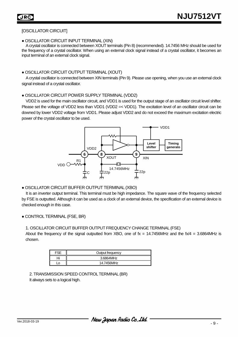
[OSCILLATOR CIRCUIT] ● OSCILLATOR CIRCUIT INPUT TERMINAL (XIN) A crystal oscillator is connected between XOUT terminals (Pin 8) (recommended). 14.7456 MHz should be used for the frequency of a crystal oscillator. When using an external clock signal instead of a crystal oscillator, it becomes an input terminal of an external clock signal. ● OSCILLATOR CIRCUIT OUTPUT TERMINAL (XOUT) A crystal oscillator is connected between XIN terminals (Pin 9). Please use opening, when you use an external clock signal instead of a crystal oscillator. ● OSCILLATOR CIRCUIT POWER SUPPLY TERMINAL (VDD2) VDD2 is used for the main oscillator circuit, and VDD1 is used for the output stage of an oscillator circuit level shifter. Please set the voltage of VDD2 less than VDD1 (VDD2 =< VDD1). The excitation level of an oscillator circuit can be downed by lower VDD2 voltage from VDD1. Please adjust VDD2 and do not exceed the maximum excitation electric power of the crystal oscillator to be used. ● OSCILLATOR CIRCUIT BUFFER OUTPUT TERMINAL (XBO) It is an inverter output terminal. This terminal must be high impedance. The square wave of the frequency selected by FSE is outputted. Although it can be used as a clock of an external device, the specification of an external device is checked enough in this case. ● CONTROL TERMINAL (FSE, BR)
1. OSCILLATOR CIRCUIT BUFFER OUTPUT FREQUENCY CHANGE TERMINAL (FSE) About the frequency of the signal outputted from XBO, one of fx = 14.7456MHz and the fx/4 = 3.6864MHz is chosen.
2. TRANSMISSION SPEED CONTROL TERMINAL (BR) It always sets to a logical high.
FSE Output frequency Hi 3.6864MHz Lo 14.7456MHz
98XOUT XIN
Level shifter
6VDD2
VDD
Timing generato
22p 22p
R1
14.7456MHz
VDD1
C
NJU7512VT
Ver.2018-03-19 - 10 -
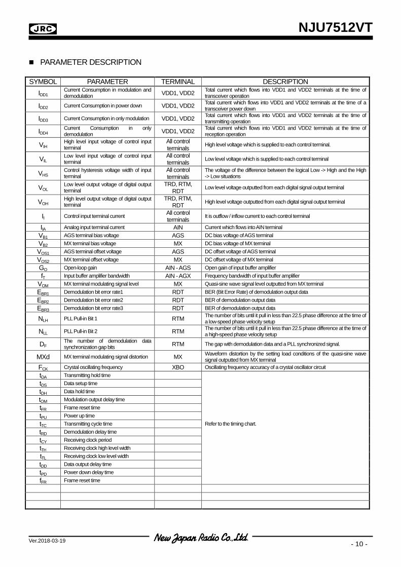
PARAMETER DESCRIPTION SYMBOL PARAMETER TERMINAL DESCRIPTION
IDD1 Current Consumption in modulation and demodulation VDD1, VDD2 Total current which flows into VDD1 and VDD2 terminals at the time of
transceiver operation
IDD2 Current Consumption in power down VDD1, VDD2 Total current which flows into VDD1 and VDD2 terminals at the time of a transceiver power down
IDD3 Current Consumption in only modulation VDD1, VDD2 Total current which flows into VDD1 and VDD2 terminals at the time of transmitting operation
IDD4 Current Consumption in only demodulation VDD1, VDD2 Total current which flows into VDD1 and VDD2 terminals at the time of
reception operation
VIH High level input voltage of control input terminal
All control terminals High level voltage which is supplied to each control terminal.
VIL Low level input voltage of control input terminal
All control terminals Low level voltage which is supplied to each control terminal
VHS Control hysteresis voltage width of input terminal
All control terminals
The voltage of the difference between the logical Low -> High and the High -> Low situations
VOL Low level output voltage of digital output terminal
TRD, RTM, RDT Low level voltage outputted from each digital signal output terminal
VOH High level output voltage of digital output terminal
TRD, RTM, RDT High level voltage outputted from each digital signal output terminal
II Control input terminal current All control terminals It is outflow / inflow current to each control terminal
IIA Analog input terminal current AIN Current which flows into AIN terminal VB1 AGS terminal bias voltage AGS DC bias voltage of AGS terminal VB2 MX terminal bias voltage MX DC bias voltage of MX terminal VOS1 AGS terminal offset voltage AGS DC offset voltage of AGS terminal VOS2 MX terminal offset voltage MX DC offset voltage of MX terminal GO Open-loop gain AIN - AGS Open gain of input buffer amplifier fT Input buffer amplifier bandwidth AIN - AGX Frequency bandwidth of input buffer amplifier
VOM MX terminal modulating signal level MX Quasi-sine wave signal level outputted from MX terminal EBR1 Demodulation bit error rate1 RDT BER (Bit Error Rate) of demodulation output data EBR2 Demodulation bit error rate2 RDT BER of demodulation output data EBR3 Demodulation bit error rate3 RDT BER of demodulation output data
NLH PLL Pull-in Bit 1 RTM The number of bits until it pull in less than 22.5 phase difference at the time of a low-speed phase velocity setup
NLL PLL Pull-in Bit 2 RTM The number of bits until it pull in less than 22.5 phase difference at the time of a high-speed phase velocity setup
DF The number of demodulation data synchronization gap bits RTM The gap with demodulation data and a PLL synchronized signal.
MXd MX terminal modulating signal distortion MX Waveform distortion by the setting load conditions of the quasi-sine wave signal outputted from MX terminal
FCK Crystal oscillating frequency XBO Oscillating frequency accuracy of a crystal oscillator circuit tDA Transmitting hold time tDS Data setup time tDH Data hold time tOM Modulation output delay time tFR Frame reset time tPU Power up time tTC Transmitting cycle time Refer to the timing chart. tRD Demodulation delay time tCY Receiving clock period tTH Receiving clock high level width tTL Receiving clock low level width tDD Data output delay time tPD Power down delay time fFR Frame reset time
NJU7512VT
Ver.2018-03-19 - 11 -
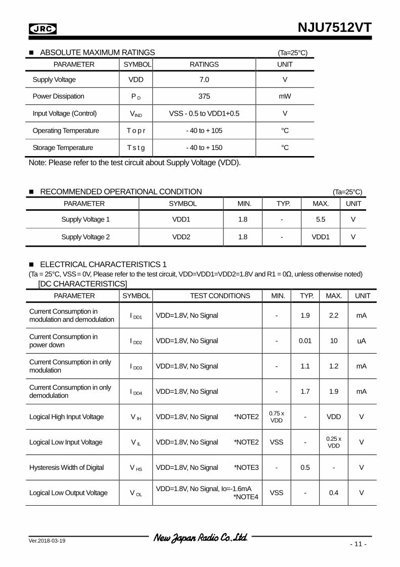
ABSOLUTE MAXIMUM RATINGS (Ta=25°C) PARAMETER SYMBOL RATINGS UNIT
Supply Voltage VDD 7.0 V
Power Dissipation P D 375 mW
Input Voltage (Control) VIND VSS - 0.5 to VDD1+0.5 V
Operating Temperature T o p r - 40 to + 105 °C
Storage Temperature T s t g - 40 to + 150 °C
Note: Please refer to the test circuit about Supply Voltage (VDD).
RECOMMENDED OPERATIONAL CONDITION (Ta=25°C) PARAMETER SYMBOL MIN. TYP. MAX. UNIT
Supply Voltage 1 VDD1 1.8 - 5.5 V
Supply Voltage 2 VDD2 1.8 - VDD1 V
ELECTRICAL CHARACTERISTICS 1 (Ta = 25°C, VSS = 0V, Please refer to the test circuit, VDD=VDD1=VDD2=1.8V and R1 = 0Ω, unless otherwise noted)
[DC CHARACTERISTICS] PARAMETER SYMBOL TEST CONDITIONS MIN. TYP. MAX. UNIT
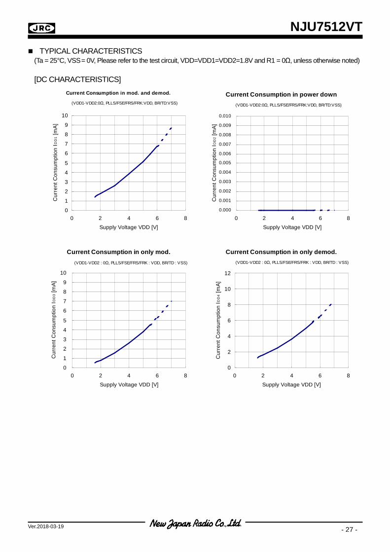
Current Consumption in modulation and demodulation I DD1 VDD=1.8V, No Signal - 1.9 2.2 mA
Current Consumption in power down I DD2 VDD=1.8V, No Signal - 0.01 10 uA
Current Consumption in only modulation I DD3 VDD=1.8V, No Signal - 1.1 1.2 mA
Current Consumption in only demodulation I DD4 VDD=1.8V, No Signal - 1.7 1.9 mA
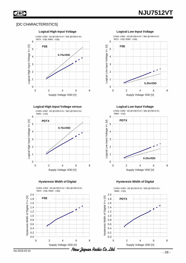
Logical High Input Voltage V IH VDD=1.8V, No Signal *NOTE2 0.75 x VDD - VDD V
Logical Low Input Voltage V IL VDD=1.8V, No Signal *NOTE2 VSS - 0.25 x VDD V
Hysteresis Width of Digital V HS VDD=1.8V, No Signal *NOTE3 - 0.5 - V
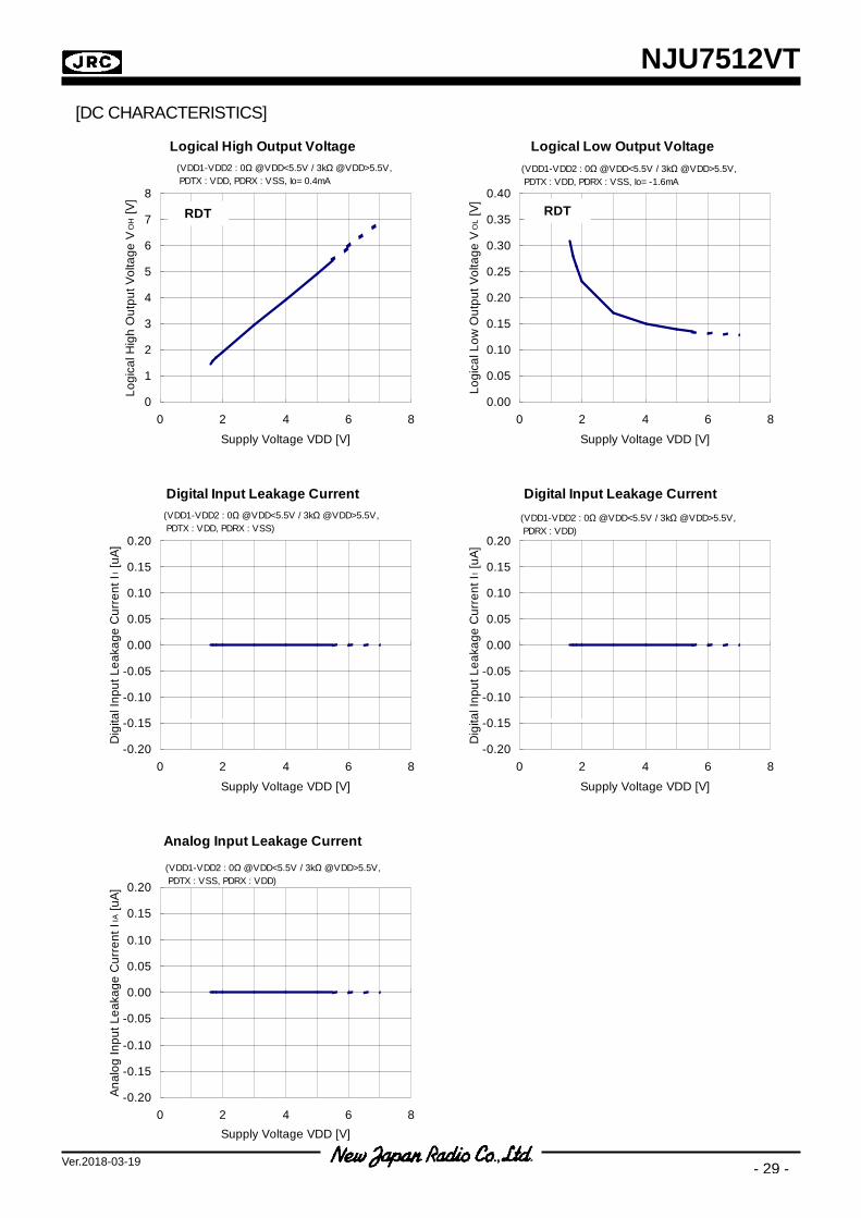
Logical Low Output Voltage V OL VDD=1.8V, No Signal, Io=-1.6mA
*NOTE4 VSS - 0.4 V
NJU7512VT
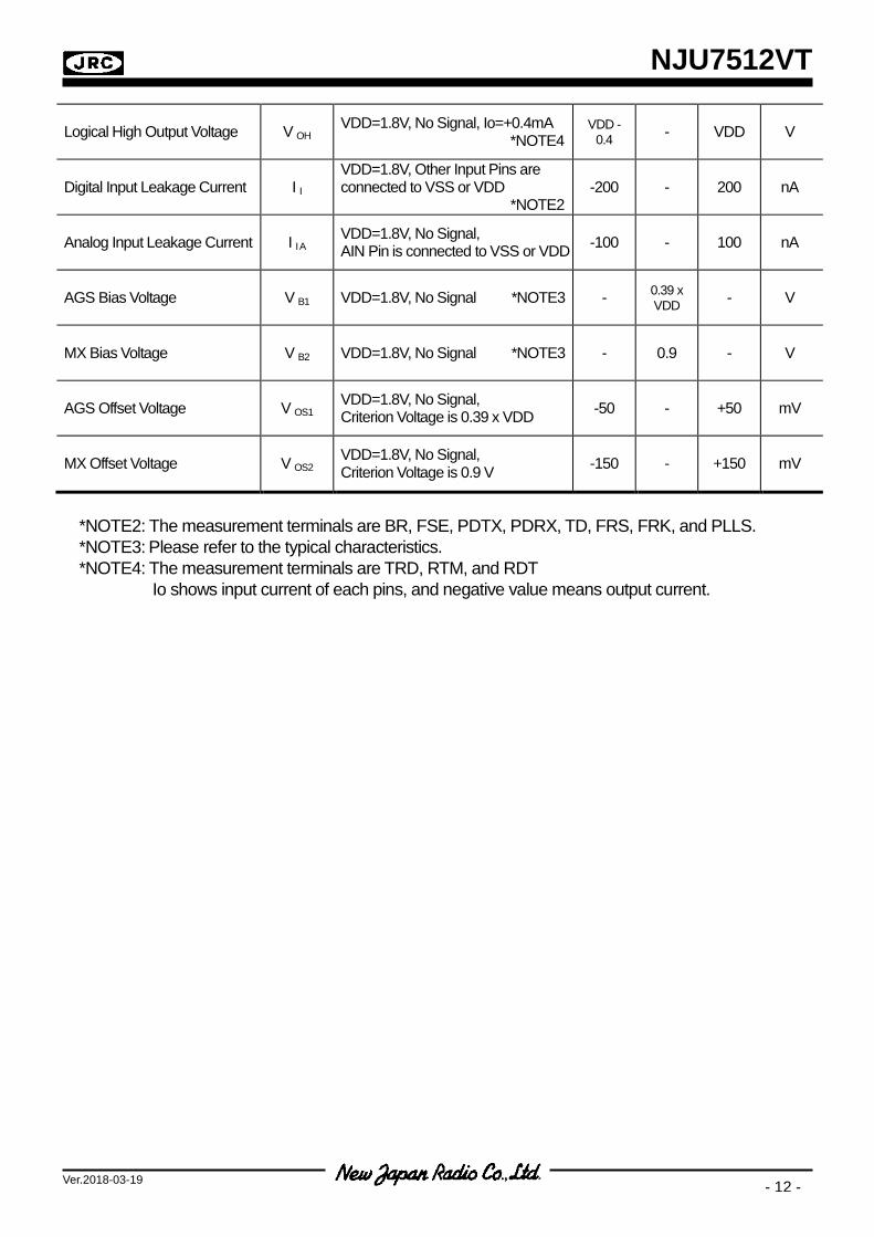
Ver.2018-03-19 - 12 -
Logical High Output Voltage V OH VDD=1.8V, No Signal, Io=+0.4mA *NOTE4
VDD - 0.4 - VDD V
Digital Input Leakage Current I I VDD=1.8V, Other Input Pins are connected to VSS or VDD *NOTE2
-200 - 200 nA
Analog Input Leakage Current I I A VDD=1.8V, No Signal, AIN Pin is connected to VSS or VDD -100 - 100 nA
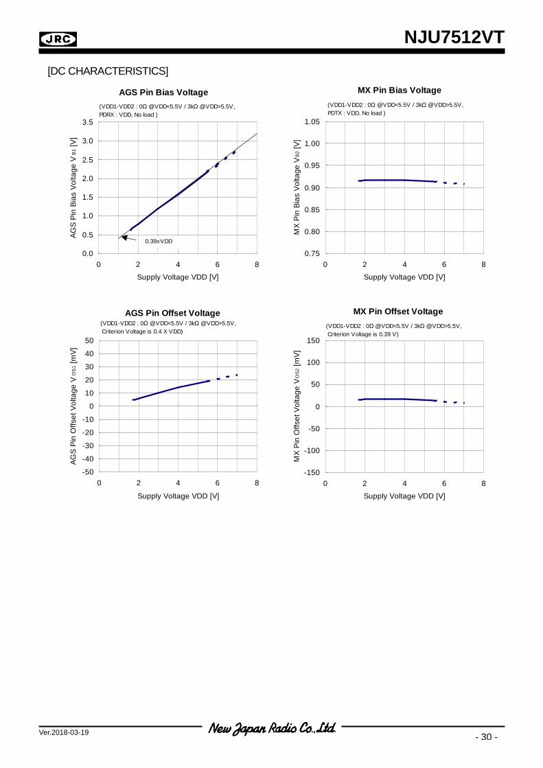
AGS Bias Voltage V B1 VDD=1.8V, No Signal *NOTE3 - 0.39 x VDD - V
MX Bias Voltage V B2 VDD=1.8V, No Signal *NOTE3 - 0.9 - V
AGS Offset Voltage V OS1 VDD=1.8V, No Signal, Criterion Voltage is 0.39 x VDD -50 - +50 mV
MX Offset Voltage V OS2 VDD=1.8V, No Signal, Criterion Voltage is 0.9 V -150 - +150 mV
*NOTE2: The measurement terminals are BR, FSE, PDTX, PDRX, TD, FRS, FRK, and PLLS. *NOTE3: Please refer to the typical characteristics. *NOTE4: The measurement terminals are TRD, RTM, and RDT
Io shows input current of each pins, and negative value means output current.
NJU7512VT
Ver.2018-03-19 - 13 -
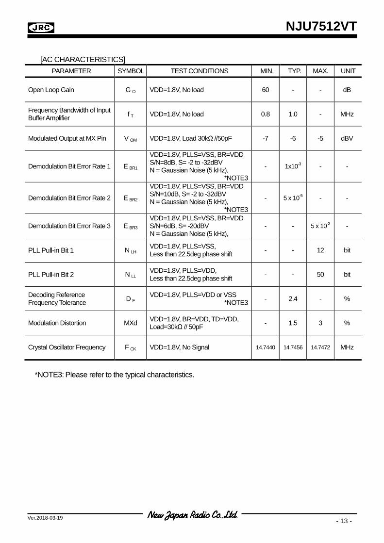
[AC CHARACTERISTICS]
PARAMETER SYMBOL TEST CONDITIONS MIN. TYP. MAX. UNIT
Open Loop Gain G O VDD=1.8V, No load 60 - - dB
Frequency Bandwidth of Input Buffer Amplifier f T VDD=1.8V, No load 0.8 1.0 - MHz
Modulated Output at MX Pin V OM VDD=1.8V, Load 30kΩ //50pF -7 -6 -5 dBV
Demodulation Bit Error Rate 1 E BR1
VDD=1.8V, PLLS=VSS, BR=VDD S/N=8dB, S= -2 to -32dBV N = Gaussian Noise (5 kHz), *NOTE3
- 1x10⁻³ - -
Demodulation Bit Error Rate 2 E BR2
VDD=1.8V, PLLS=VSS, BR=VDD S/N=10dB, S= -2 to -32dBV N = Gaussian Noise (5 kHz), *NOTE3
- 5 x 10⁻⁵ - -
Demodulation Bit Error Rate 3 E BR3 VDD=1.8V, PLLS=VSS, BR=VDD S/N=6dB, S= -20dBV N = Gaussian Noise (5 kHz),
- - 5 x 10⁻² -
PLL Pull-in Bit 1 N LH VDD=1.8V, PLLS=VSS, Less than 22.5deg phase shift - - 12 bit
PLL Pull-in Bit 2 N LL VDD=1.8V, PLLS=VDD, Less than 22.5deg phase shift - - 50 bit
Decoding Reference Frequency Tolerance D F
VDD=1.8V, PLLS=VDD or VSS *NOTE3 - 2.4 - %
Modulation Distortion MXd VDD=1.8V, BR=VDD, TD=VDD, Load=30kΩ // 50pF - 1.5 3 %
Crystal Oscillator Frequency F CK VDD=1.8V, No Signal 14.7440 14.7456 14.7472 MHz
*NOTE3: Please refer to the typical characteristics.
NJU7512VT
Ver.2018-03-19 - 14 -
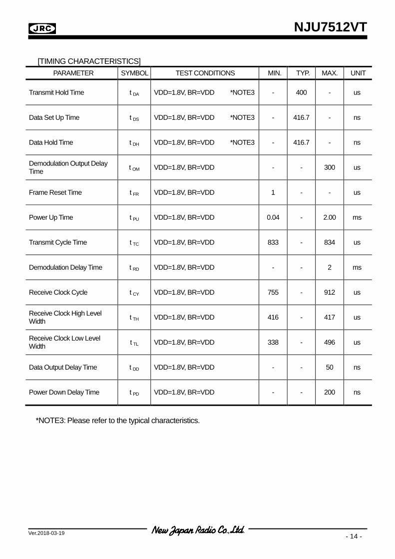
[TIMING CHARACTERISTICS]
PARAMETER SYMBOL TEST CONDITIONS MIN. TYP. MAX. UNIT
Transmit Hold Time t DA VDD=1.8V, BR=VDD *NOTE3 - 400 - us
Data Set Up Time t DS VDD=1.8V, BR=VDD *NOTE3 - 416.7 - ns
Data Hold Time t DH VDD=1.8V, BR=VDD *NOTE3 - 416.7 - ns
Demodulation Output Delay Time t OM VDD=1.8V, BR=VDD - - 300 us
Frame Reset Time t FR VDD=1.8V, BR=VDD 1 - - us
Power Up Time t PU VDD=1.8V, BR=VDD 0.04 - 2.00 ms
Transmit Cycle Time t TC VDD=1.8V, BR=VDD 833 - 834 us
Demodulation Delay Time t RD VDD=1.8V, BR=VDD - - 2 ms
Receive Clock Cycle t CY VDD=1.8V, BR=VDD 755 - 912 us
Receive Clock High Level Width t TH VDD=1.8V, BR=VDD 416 - 417 us
Receive Clock Low Level Width t TL VDD=1.8V, BR=VDD 338 - 496 us
Data Output Delay Time t DD VDD=1.8V, BR=VDD - - 50 ns
Power Down Delay Time t PD VDD=1.8V, BR=VDD - - 200 ns
*NOTE3: Please refer to the typical characteristics.
NJU7512VT
Ver.2018-03-19 - 15 -
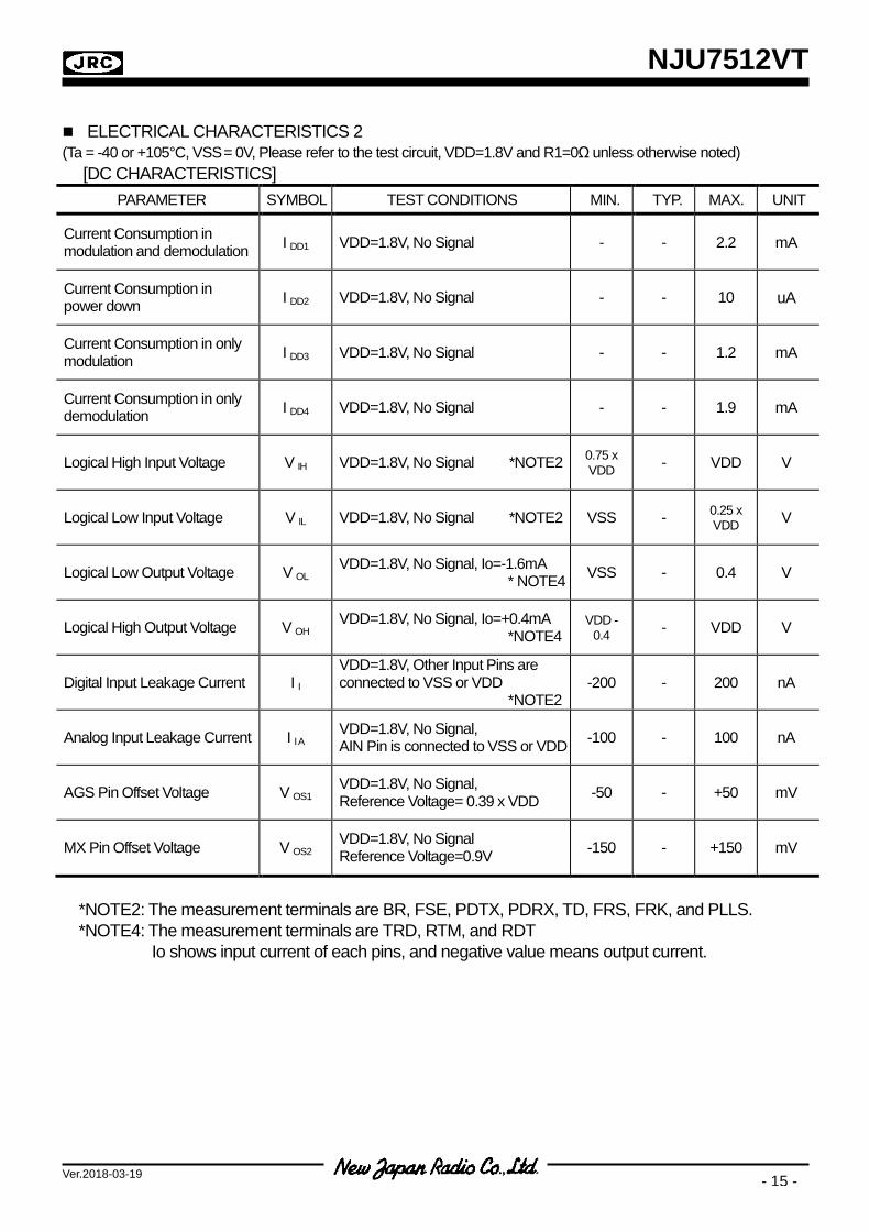
ELECTRICAL CHARACTERISTICS 2 (Ta = -40 or +105°C, VSS = 0V, Please refer to the test circuit, VDD=1.8V and R1=0Ω unless otherwise noted)
[DC CHARACTERISTICS] PARAMETER SYMBOL TEST CONDITIONS MIN. TYP. MAX. UNIT
Current Consumption in modulation and demodulation I DD1 VDD=1.8V, No Signal - - 2.2 mA
Current Consumption in power down I DD2 VDD=1.8V, No Signal - - 10 uA
Current Consumption in only modulation I DD3 VDD=1.8V, No Signal - - 1.2 mA
Current Consumption in only demodulation I DD4 VDD=1.8V, No Signal - - 1.9 mA
Logical High Input Voltage V IH VDD=1.8V, No Signal *NOTE2 0.75 x VDD - VDD V
Logical Low Input Voltage V IL VDD=1.8V, No Signal *NOTE2 VSS - 0.25 x VDD V
Logical Low Output Voltage V OL VDD=1.8V, No Signal, Io=-1.6mA
* NOTE4 VSS - 0.4 V
Logical High Output Voltage V OH VDD=1.8V, No Signal, Io=+0.4mA *NOTE4
VDD - 0.4 - VDD V
Digital Input Leakage Current I I VDD=1.8V, Other Input Pins are connected to VSS or VDD *NOTE2
-200 - 200 nA
Analog Input Leakage Current I I A VDD=1.8V, No Signal, AIN Pin is connected to VSS or VDD -100 - 100 nA
AGS Pin Offset Voltage V OS1 VDD=1.8V, No Signal, Reference Voltage= 0.39 x VDD -50 - +50 mV
MX Pin Offset Voltage V OS2 VDD=1.8V, No Signal Reference Voltage=0.9V -150 - +150 mV
*NOTE2: The measurement terminals are BR, FSE, PDTX, PDRX, TD, FRS, FRK, and PLLS. *NOTE4: The measurement terminals are TRD, RTM, and RDT
Io shows input current of each pins, and negative value means output current.
NJU7512VT
Ver.2018-03-19 - 16 -
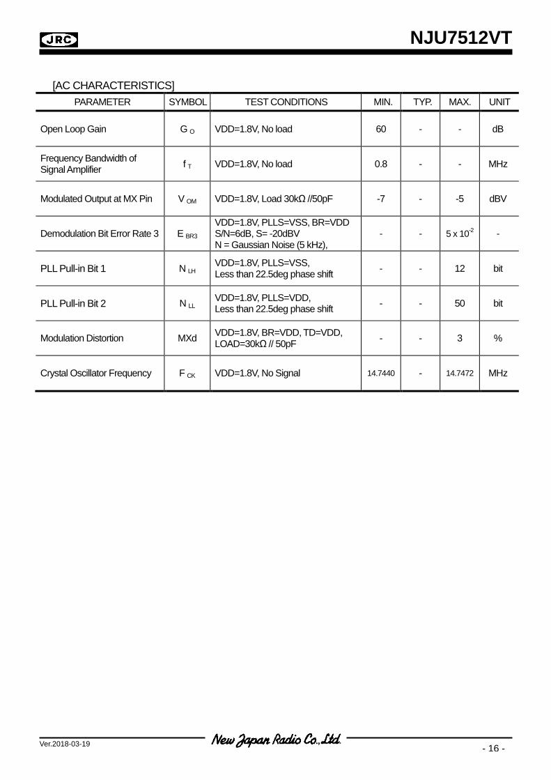
[AC CHARACTERISTICS]
PARAMETER SYMBOL TEST CONDITIONS MIN. TYP. MAX. UNIT
Open Loop Gain G O VDD=1.8V, No load 60 - - dB
Frequency Bandwidth of Signal Amplifier f T VDD=1.8V, No load 0.8 - - MHz
Modulated Output at MX Pin V OM VDD=1.8V, Load 30kΩ //50pF -7 - -5 dBV
Demodulation Bit Error Rate 3 E BR3 VDD=1.8V, PLLS=VSS, BR=VDD S/N=6dB, S= -20dBV N = Gaussian Noise (5 kHz),
- - 5 x 10⁻² -
PLL Pull-in Bit 1 N LH VDD=1.8V, PLLS=VSS, Less than 22.5deg phase shift - - 12 bit
PLL Pull-in Bit 2 N LL VDD=1.8V, PLLS=VDD, Less than 22.5deg phase shift - - 50 bit
Modulation Distortion MXd VDD=1.8V, BR=VDD, TD=VDD, LOAD=30kΩ // 50pF - - 3 %
Crystal Oscillator Frequency F CK VDD=1.8V, No Signal 14.7440 - 14.7472 MHz
NJU7512VT
Ver.2018-03-19 - 17 -
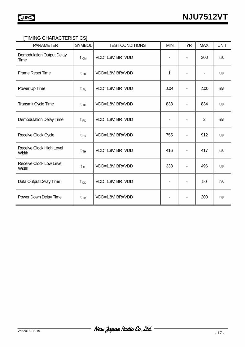
[TIMING CHARACTERISTICS]
PARAMETER SYMBOL TEST CONDITIONS MIN. TYP. MAX. UNIT
Demodulation Output Delay Time t OM VDD=1.8V, BR=VDD - - 300 us
Frame Reset Time t FR VDD=1.8V, BR=VDD 1 - - us
Power Up Time t PU VDD=1.8V, BR=VDD 0.04 - 2.00 ms
Transmit Cycle Time t TC VDD=1.8V, BR=VDD 833 - 834 us
Demodulation Delay Time t RD VDD=1.8V, BR=VDD - - 2 ms
Receive Clock Cycle t CY VDD=1.8V, BR=VDD 755 - 912 us
Receive Clock High Level Width t TH VDD=1.8V, BR=VDD 416 - 417 us
Receive Clock Low Level Width t TL VDD=1.8V, BR=VDD 338 - 496 us
Data Output Delay Time t DD VDD=1.8V, BR=VDD - - 50 ns
Power Down Delay Time t PD VDD=1.8V, BR=VDD - - 200 ns
NJU7512VT
Ver.2018-03-19 - 18 -
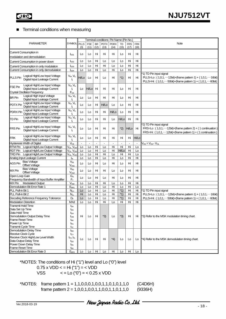
Terminal conditions when measuring
PARAMETER SYMBOL Terminal conditions: Pin Name (Pin No.)
Note PLLS (3)
FSE (11)
BR (12)
PDTX (13)
PDRX (14)
TD (15)
FRS (17)
FRK (18)
Current Consumption in modulation and demodulation
IDD1 Lo Lo Hi Hi Hi Lo Hi Hi
Current Consumption in power down IDD2 Lo Lo Hi Lo Lo Lo Hi Hi Current Consumption in only modulation IDD3 Lo Lo Hi Hi Lo Lo Hi Hi Current Consumption in only demodulation IDD4 Lo Lo Hi Lo Hi Lo Hi Hi
PLLS Pin Logical High/Low Input Voltage Digital Input Leakage Current
VIH , VIL II
Hi/Lo Lo Hi Lo Hi *1) Hi Hi *1) TD Pin input signal PLLS=Lo : ( 1,0,1,・・・12bit)+(frame pattern 1) + ( 1,0,1,・・・16bit) PLLS=Hi : ( 1,0,1,・・・50bit)+(frame pattern 1) + ( 1,0,1,・・・60bit)
FSE Pin Logical High/Low Input Voltage Digital Input Leakage Current
VIH , VIL II
FCK Lo Hi/Lo Hi Hi Hi Lo Hi Hi
Crystal Oscillator Frequency
BR Pin Logical High Input Voltage Digital Input Leakage Current
VIH , VIL II
Lo Lo Hi Hi Hi Lo Hi Hi
PDTX Pin Logical High/Low Input Voltage Digital Input Leakage Current
VIH , VIL II
Lo Lo Hi Hi/Lo Lo Lo Hi Hi
PDRX Pin Logical High/Low Input Voltage Digital Input Leakage Current
VIH , VIL II
Lo Lo Hi Hi Hi/Lo Lo Hi Hi
TD Pin Logical High/Low Input Voltage Digital Input Leakage Current
VIH , VIL II
Lo Lo Hi Hi Lo Hi/Lo Hi Hi
FRS Pin Logical High/Low Input Voltage Digital Input Leakage Current
VIH , VIL II
Lo Lo Hi Hi Hi *2) Hi/Lo Hi *2) TD Pin input signal FRS=Lo : ( 1,0,1,・・・12bit)+(frame pattern 2) + ( 1 continuation ) FRS=Hi : ( 1,0,1,・・・12bit)+(frame pattern 1) + ( 1 continuation )
FRK Logical High/Low Input Voltage Digital Input Leakage Current
VIH , VIL II
Lo Lo Hi Hi Hi Hi Hi Hi/Lo
Hysteresis Width of Digital VHS - - - - - - - - VHS = VOH - VOL RTM Pin Logical High/Low Output Voltage VOL , VOH Lo Lo Hi Lo Hi Hi Hi Lo RDT Pin Logical High/Low Output Voltage VOL , VOH Lo Lo Hi Lo Hi Hi/Lo Hi Lo TRD Pin Logical High/Low Output Voltage VOL , VOH Lo Lo Hi Hi Lo Hi Hi Lo Analog Input Leakage Current IIA Lo Lo Hi Lo Hi Lo Hi Hi
AGS Pin Bias Voltage Offset Voltage
VB1 VOS1
Lo Lo Hi Lo Hi Lo Hi Hi
MX Pin Bias Voltage Offset Voltage
VB2 VOS2
Lo Lo Hi Hi Lo Lo Hi Hi
Open Loop Gain Frequency Bandwidth of Input Buffer Amplifier
GO FT
Lo Lo Hi Lo Hi Lo Hi Hi
MX Pin Modulated Output VOM Lo Lo Hi Hi Lo Lo Hi Hi Demodulation Bit Error Rate 1 EBR1 Lo Lo Hi Lo Hi Lo Hi Lo PLL Pull-in Bit 1 NLH Lo Lo Hi Lo Hi *1) Hi Hi *1) TD Pin input signal
PLLS=Lo : ( 1,0,1,・・・12bit)+(frame pattern 1) + ( 1,0,1,・・・16bit) PLLS=Hi : ( 1,0,1,・・・50bit)+(frame pattern 1) + ( 1,0,1,・・・60bit)
PLL Pull-in Bit 2 NLL Hi Lo Hi Lo Hi *1) Hi Hi Decoding Reference Frequency Tolerance DF Lo Lo Hi Lo Hi *1) Hi Hi Modulation Distortion MXd Lo Lo Hi Hi Lo Hi Hi Hi Transmit Hold Time Data Set Up Time Data Hold Time Demodulation Output Delay Time Frame Reset Time Power Up Time Transmit Cycle Time
tDA tDS tDH tOM tFR tPU tTC
Hi Lo Hi *3) Lo *3) Hi Hi *3) Refer to the MSK modulation timing chart.
Demodulation Delay Time Receive Clock Cycle Receive Clock High/Low Level Width Data Output Delay Time Power Down Delay Time Frame Reset Time
tRD tCY
tTH , tTL tDD tPD tFR
Lo Lo Hi Hi *4) Lo Lo Lo *4) Refer to the MSK demodulation timing chart.
Demodulation Bit Error Rate 3 EBR3 Lo Lo Hi Lo Hi Lo Hi Lo
*NOTE5: The conditions of Hi (“1”) level and Lo (“0”) level 0.75 x VDD < = Hi (“1”) = < VDD VSS < = Lo (“0”) = < 0.25 x VDD *NOTE6: frame pattern 1 = 1,1,0,0,0,1,0,0,1,1,0,1,0,1,1,0 (C4D6H) frame pattern 2 = 1,0,0,1,0,0,1,1,0,0,1,1,0,1,1,0 (9336H)
NJU7512VT
Ver.2018-03-19 - 19 -
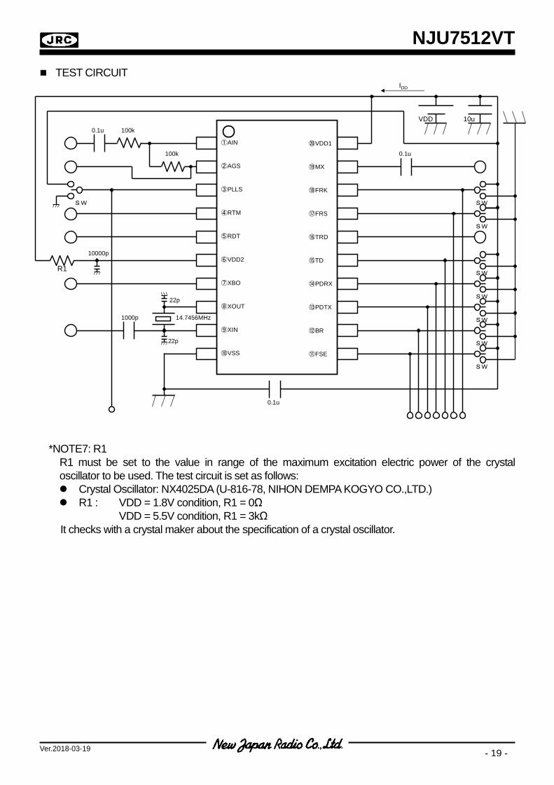
TEST CIRCUIT
*NOTE7: R1
R1 must be set to the value in range of the maximum excitation electric power of the crystal oscillator to be used. The test circuit is set as follows: Crystal Oscillator: NX4025DA (U-816-78, NIHON DEMPA KOGYO CO.,LTD.) R1 : VDD = 1.8V condition, R1 = 0Ω
VDD = 5.5V condition, R1 = 3kΩ It checks with a crystal maker about the specification of a crystal oscillator.
①AIN
③PLLS
④RTM
⑤RDT
⑥VDD2
⑦XBO
⑧XOUT
⑨XIN
②AGS
⑫BR
⑬PDTX
⑭PDRX
⑮TD
⑯TRD
⑰FRS
⑱FRK
⑲MX
⑩VSS ⑪FSE
⑳VDD1
VDD
14.7456MHz
SW
SW
SW
SW
SW
SWSW
SW
0.1u 100k
100k
1000p
10000p
0.1u
0.1u
22p
22p
IDD
10u
R1
NJU7512VT
Ver.2018-03-19 - 20 -
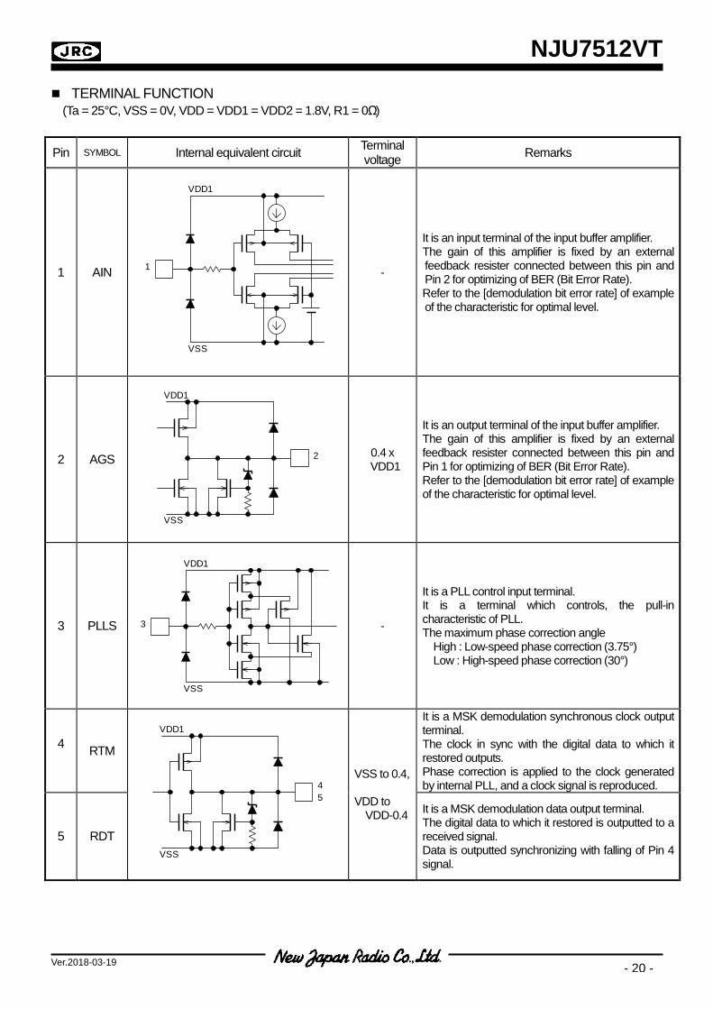
TERMINAL FUNCTION (Ta = 25°C, VSS = 0V, VDD = VDD1 = VDD2 = 1.8V, R1 = 0Ω)
Pin SYMBOL Internal equivalent circuit Terminal voltage Remarks
1 AIN
-
It is an input terminal of the input buffer amplifier. The gain of this amplifier is fixed by an external feedback resister connected between this pin and Pin 2 for optimizing of BER (Bit Error Rate). Refer to the [demodulation bit error rate] of example of the characteristic for optimal level.
2 AGS
0.4 x VDD1
It is an output terminal of the input buffer amplifier. The gain of this amplifier is fixed by an external feedback resister connected between this pin and Pin 1 for optimizing of BER (Bit Error Rate). Refer to the [demodulation bit error rate] of example of the characteristic for optimal level.
3 PLLS
-
It is a PLL control input terminal. It is a terminal which controls, the pull-in characteristic of PLL. The maximum phase correction angle
High : Low-speed phase correction (3.75°) Low : High-speed phase correction (30°)
4 RTM
VSS to 0.4, VDD to
VDD-0.4
It is a MSK demodulation synchronous clock output terminal. The clock in sync with the digital data to which it restored outputs. Phase correction is applied to the clock generated by internal PLL, and a clock signal is reproduced.
5 RDT
It is a MSK demodulation data output terminal. The digital data to which it restored is outputted to a received signal. Data is outputted synchronizing with falling of Pin 4 signal.
VDD1
1
VSS
2
VSS
VDD1
VSS
3
VDD1
45
VSS
VDD1
NJU7512VT
Ver.2018-03-19 - 21 -
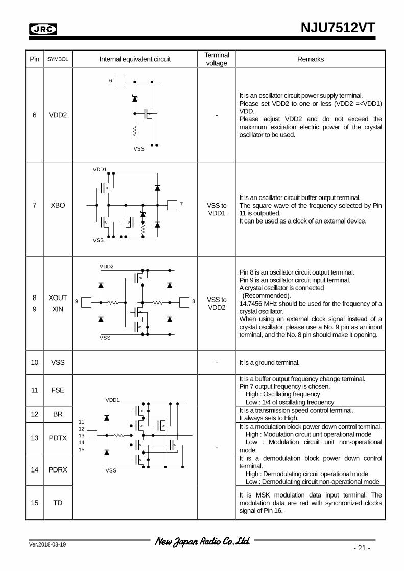
Pin SYMBOL Internal equivalent circuit Terminal voltage Remarks
6 VDD2
-
It is an oscillator circuit power supply terminal. Please set VDD2 to one or less (VDD2 =<VDD1) VDD. Please adjust VDD2 and do not exceed the maximum excitation electric power of the crystal oscillator to be used.
7
XBO
VSS to VDD1
It is an oscillator circuit buffer output terminal. The square wave of the frequency selected by Pin 11 is outputted. It can be used as a clock of an external device.
8
9 XOUT
XIN
VSS to VDD2
Pin 8 is an oscillator circuit output terminal. Pin 9 is an oscillator circuit input terminal. A crystal oscillator is connected (Recommended). 14.7456 MHz should be used for the frequency of a crystal oscillator. When using an external clock signal instead of a crystal oscillator, please use a No. 9 pin as an input terminal, and the No. 8 pin should make it opening.
10 VSS
- It is a ground terminal.
11 FSE
-
It is a buffer output frequency change terminal. Pin 7 output frequency is chosen.
High : Oscillating frequency Low : 1/4 of oscillating frequency
12 BR It is a transmission speed control terminal. It always sets to High.
13 PDTX It is a modulation block power down control terminal.
High : Modulation circuit unit operational mode Low : Modulation circuit unit non-operational
mode
14 PDRX It is a demodulation block power down control terminal.
High : Demodulating circuit operational mode Low : Demodulating circuit non-operational mode
15 TD
It is MSK modulation data input terminal. The modulation data are red with synchronized clocks signal of Pin 16.
VSS
6
7
VSS
VDD1
9 8
VSS
VDD2
VSS
1112131415
VDD1
NJU7512VT
Ver.2018-03-19 - 22 -
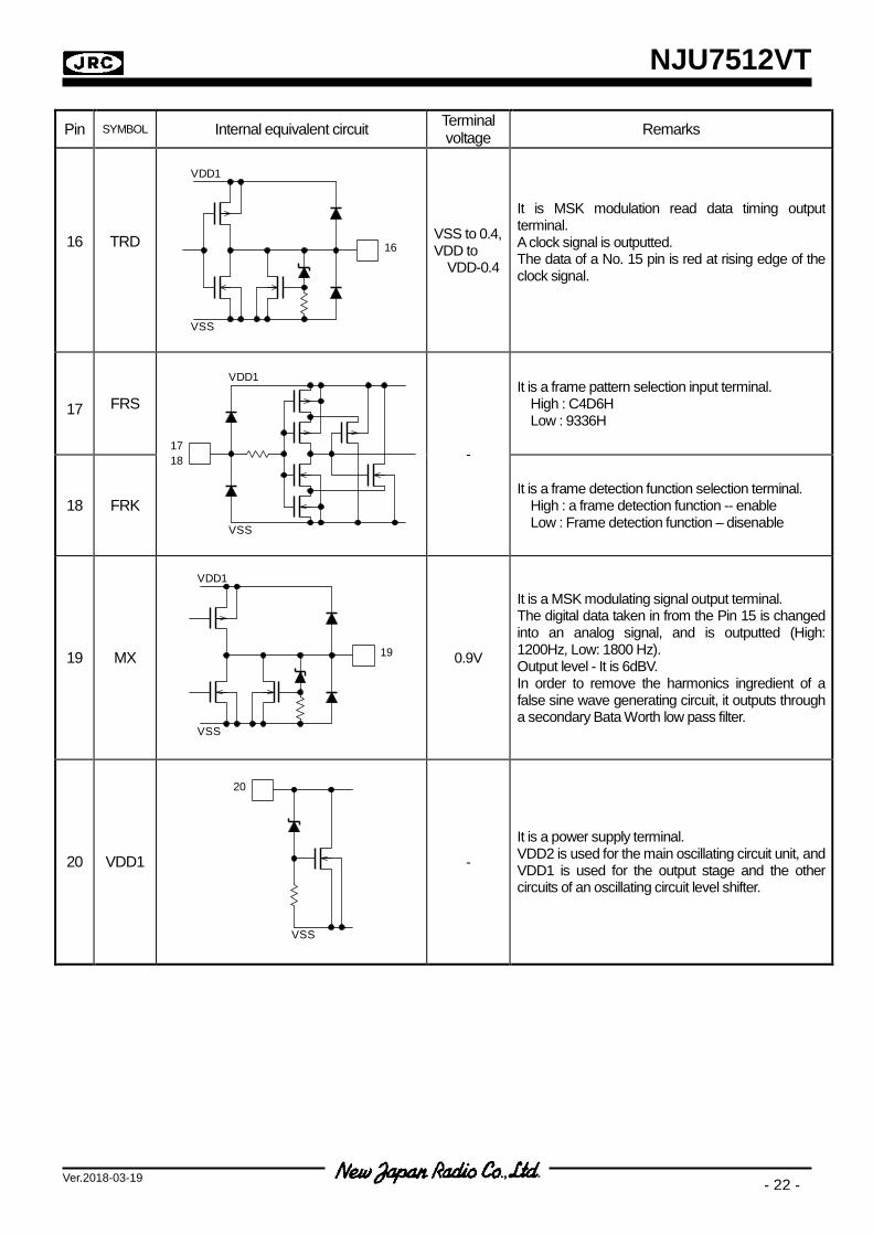
Pin SYMBOL Internal equivalent circuit Terminal voltage Remarks
16
TRD
VSS to 0.4, VDD to
VDD-0.4
It is MSK modulation read data timing output terminal. A clock signal is outputted. The data of a No. 15 pin is red at rising edge of the clock signal.
17
FRS
-
It is a frame pattern selection input terminal. High : C4D6H Low : 9336H
18 FRK
It is a frame detection function selection terminal. High : a frame detection function -- enable Low : Frame detection function – disenable
19 MX
0.9V
It is a MSK modulating signal output terminal. The digital data taken in from the Pin 15 is changed into an analog signal, and is outputted (High: 1200Hz, Low: 1800 Hz). Output level - It is 6dBV. In order to remove the harmonics ingredient of a false sine wave generating circuit, it outputs through a secondary Bata Worth low pass filter.
20 VDD1
-
It is a power supply terminal. VDD2 is used for the main oscillating circuit unit, and VDD1 is used for the output stage and the other circuits of an oscillating circuit level shifter.
16
VSS
VDD1
VSS
1718
VDD1
19
VSS
VDD1
VSS
20

NJU7512VT
Ver.2018-03-19 - 23 -
TIMING CHART
tDS
tPU
tOM
tDH
tFR
tPUtDA
1 1 0 1 1 0 1 0
PDTX
Internal timing
TRD
MX
ModulationData
MSK modulation timing chart
tTC
1
TD
:don't care
tPD
tTH
tFR
tRD
1 0 11 0 0 1
PDRX
ModulationData
MSK demodulation timing chart
Preamble pattern +16-bit frame pattern
tCY
tDDtTL
AGS
Internalsynchronous clock
Internaldemodulati
on Data
RTM
RDT
:don't care
Preamble pattern +16-bit frame pattern 1 0 11 0 0 1
NJU7512VT
Ver.2018-03-19 - 24 -
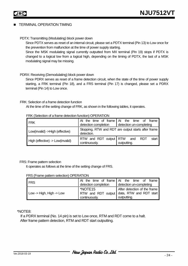
TERMINAL OPERATION TIMING
PDTX: Transmitting (Modulating) block power down Since PDTX serves as reset of an internal circuit, please set a PDTX terminal (Pin 13) to Low once for the prevention from malfunction at the time of power supply starting. Since the MSK modulating signal currently outputted from MX terminal (Pin 19) stops if PDTX is changed to a logical low from a logical high, depending on the timing of PDTX, the last of a MSK modulating signal may be missing.
PDRX: Receiving (Demodulating) block power down Since PDRX serves as reset of a frame detection circuit, when the state of the time of power supply starting, a FRK terminal (Pin 18), and a FRS terminal (Pin 17) is changed, please set a PDRX terminal (Pin 14) to Low once.
FRK: Selection of a frame detection function At the time of the setting change of FRK, as shown in the following tables, it operates. FRK (Selection of a frame detection function) OPERATION
FRK At the time of frame detection completion
At the time of frame detection un-completing
Low(invalid) ->High (effective) Stopping, RTW and RDT are output starts after frame detection.
High (effective) -> Low(invalid) RTW and RDT output continuously.
RTW and RDT start outputting.
FRS: Frame pattern selection It operates as follows at the time of the setting change of FRS.
FRS (Frame pattern selection) OPERATION
FRS At the time of frame detection completion
At the time of frame detection un-completing
Low -> High, High -> Low *NOTE15 RTW and RDT output continuously.
After detection of the frame data, RTW and RDT start outputting.
*NOTE8: If a PDRX terminal (No. 14 pin) is set to Low once, RTM and RDT come to a halt. After frame pattern detection, RTM and RDT start outputting.
NJU7512VT
Ver.2018-03-19 - 25 -
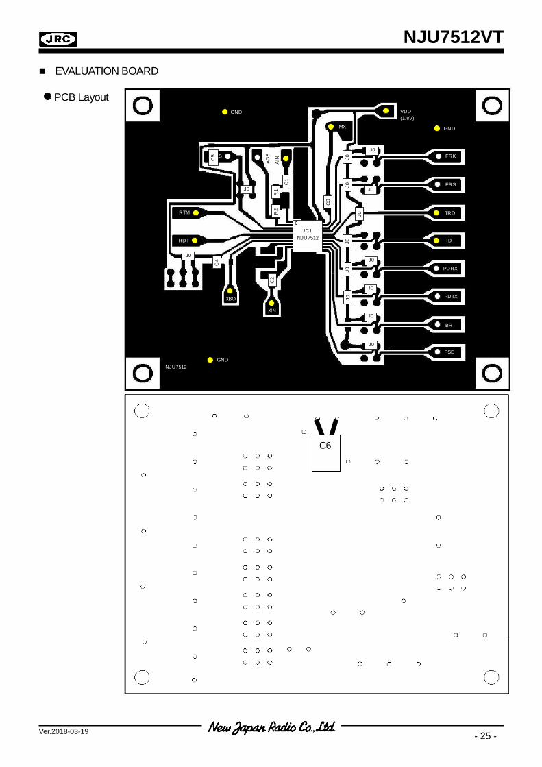
EVALUATION BOARD PCB Layout
IC1NJU7512
J0
J0
C2
C1
R1
R2
J0J0
J0
J0J0
C4
C3
VDD
AIN
AGSPLLS
RTM
RDT
XBO
XIN
FSE
BR
PDTX
PDRX
TD
TRD
FRS
FRK
MX
NJU7512
C5
J0
J0
J0
J0
J0
J0
(1.8V)
J0
GND
GND
GND
C6
NJU7512VT
Ver.2018-03-19 - 26 -
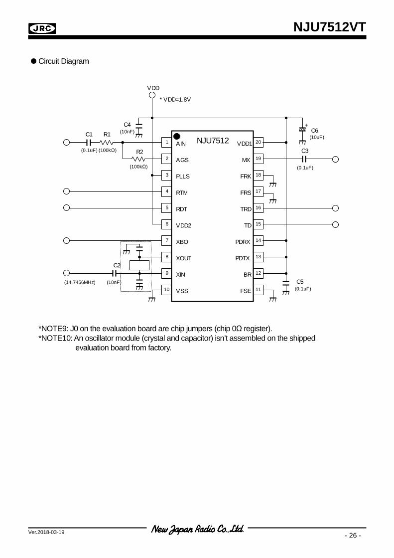
Circuit Diagram *NOTE9: J0 on the evaluation board are chip jumpers (chip 0Ω register). *NOTE10: An oscillator module (crystal and capacitor) isn’t assembled on the shipped evaluation board from factory.
AIN
PLLS
RTM
RDT
XOUT
XIN
XBO
VSS
VDD2
AGS
FRS
FRK
MX
VDD1
BR
PDTX
PDRX
TD
TRD
FSE
1
+
(10nF)(0.1uF)
(10uF)
(14.7456MHz)
(0.1uF)
(100kΩ)(0.1uF)
VDD
C1 R1
R2
NJU7512
C2
(100kΩ)
C4
C3
C6
C5
(10nF)
20
19
18
17
16
15
14
13
12
11
2
3
4
5
6
7
8
9
10
* VDD=1.8V
NJU7512VT
Ver.2018-03-19 - 27 -
TYPICAL CHARACTERISTICS (Ta = 25°C, VSS = 0V, Please refer to the test circuit, VDD=VDD1=VDD2=1.8V and R1 = 0Ω, unless otherwise noted) [DC CHARACTERISTICS]
Current Consumption in mod. and demod.
0
1
2
3
4
5
6
7
8
9
10
0 2 4 6 8Supply Voltage VDD [V]
Cur
rent
Con
sum
ptio
n I D
D1 [
mA]
(VDD1-VDD2:0Ω, PLLS/FSE/FRS/FRK:VDD, BR/TD:VSS)
Current Consumption in power down
0.000
0.001
0.002
0.003
0.004
0.005
0.006
0.007
0.008
0.009
0.010
0 2 4 6 8Supply Voltage VDD [V]
Cur
rent
Con
sum
ptio
n I D
D2 [
mA]
(VDD1-VDD2:0Ω, PLLS/FSE/FRS/FRK:VDD, BR/TD:VSS)
Current Consumption in only mod.
0
1
2
3
4
5
6
7
8
9
10
0 2 4 6 8Supply Voltage VDD [V]
Cur
rent
Con
sum
ptio
n I D
D3 [
mA]
(VDD1-VDD2 : 0Ω, PLLS/FSE/FRS/FRK : VDD, BR/TD : VSS)
Current Consumption in only demod.
0
2
4
6
8
10
12
0 2 4 6 8Supply Voltage VDD [V]
Cur
rent
Con
sum
ptio
n I D
D4 [
mA]
(VDD1-VDD2 : 0Ω, PLLS/FSE/FRS/FRK : VDD, BR/TD : VSS)
NJU7512VT
Ver.2018-03-19 - 28 -
[DC CHARACTERISTICS]
Logical High Input Voltage versus
0
1
2
3
4
5
6
0 2 4 6 8Supply Voltage VDD [V]
Logi
cal H
igh
Inpu
t Vol
tage
V IH
[V]
0.75xVDD
(VDD1-VDD2 : 0Ω @VDD<5.5V / 3kΩ @VDD>5.5V, PDRX : VSS)
PDTX
Logical Low Input Voltage
0
1
2
3
4
5
6
0 2 4 6 8Supply Voltage VDD [V]
Logi
cal L
ow In
put V
olta
ge V
IL [V
]
(VDD1-VDD2 : 0Ω @VDD<5.5V / 3kΩ @VDD>5.5V, PDRX : VSS)
0.25xVDD
PDTX
Logical High Input Voltage
0
1
2
3
4
5
6
0 2 4 6 8Supply Voltage VDD [V]
Logi
cal H
igh
Inpu
t Vol
tage
V IH
[V]
(VDD1-VDD2 : 0Ω @VDD<5.5V / 3kΩ @VDD>5.5V, PDTX : VDD, PDRX : VDD)
0.75xVDD
Logical Low Input Voltage
0
1
2
3
4
5
6
0 2 4 6 8Supply Voltage VDD [V]
Logi
cal L
ow In
put V
olta
ge V
IL [V
]
(VDD1-VDD2 : 0Ω @VDD<5.5V / 3kΩ @VDD>5.5V, PDTX : VDD, PDRX : VDD)
0.25xVDD
FSE
Hysteresis Width of Digital
0.00.20.40.60.81.01.21.41.61.82.0
0 2 4 6 8Supply Voltage VDD [V]
Hys
tere
sis
Wid
th o
f Dig
ital V
HS
[V]
(VDD1-VDD2 : 0Ω @VDD<5.5V / 3kΩ @VDD>5.5V, PDTX : VDD, PDRX : VDD)
FSE
Hysteresis Width of Digital
0.00.20.40.60.81.01.21.41.61.82.0
0 2 4 6 8Supply Voltage VDD [V]
Hys
tere
sis
Wid
th o
f Dig
ital V
HS
[V]
(VDD1-VDD2 : 0Ω @VDD<5.5V / 3kΩ @VDD>5.5V, PDRX : VSS)
PDTX
FSE
NJU7512VT
Ver.2018-03-19 - 29 -
[DC CHARACTERISTICS]
Logical High Output Voltage
0
1
2
3
4
5
6
7
8
0 2 4 6 8Supply Voltage VDD [V]
Logi
cal H
igh
Out
put V
olta
ge V
OH [V
]
RDT
(VDD1-VDD2 : 0Ω @VDD<5.5V / 3kΩ @VDD>5.5V, PDTX : VDD, PDRX : VSS, Io= 0.4mA
Logical Low Output Voltage
0.00
0.05
0.10
0.15
0.20
0.25
0.30
0.35
0.40
0 2 4 6 8Supply Voltage VDD [V]
Logi
cal L
ow O
utpu
t Vol
tage
V O
L [V]
(VDD1-VDD2 : 0Ω @VDD<5.5V / 3kΩ @VDD>5.5V, PDTX : VDD, PDRX : VSS, Io= -1.6mA
RDT
Digital Input Leakage Current
-0.20
-0.15
-0.10
-0.05
0.00
0.05
0.10
0.15
0.20
0 2 4 6 8Supply Voltage VDD [V]
Dig
ital I
nput
Lea
kage
Cur
rent
I I [
uA]
FSE
(VDD1-VDD2 : 0Ω @VDD<5.5V / 3kΩ @VDD>5.5V, PDTX : VDD, PDRX : VSS)
Digital Input Leakage Current
-0.20
-0.15
-0.10
-0.05
0.00
0.05
0.10
0.15
0.20
0 2 4 6 8Supply Voltage VDD [V]
Dig
ital I
nput
Lea
kage
Cur
rent
I I [u
A]
PDTX
(VDD1-VDD2 : 0Ω @VDD<5.5V / 3kΩ @VDD>5.5V, PDRX : VDD)
Analog Input Leakage Current
-0.20
-0.15
-0.10
-0.05
0.00
0.05
0.10
0.15
0.20
0 2 4 6 8Supply Voltage VDD [V]
Anal
og In
put L
eaka
ge C
urre
nt I
IA [u
A]
(VDD1-VDD2 : 0Ω @VDD<5.5V / 3kΩ @VDD>5.5V, PDTX : VSS, PDRX : VDD)
NJU7512VT
Ver.2018-03-19 - 30 -
[DC CHARACTERISTICS]
AGS Pin Bias Voltage
0.0
0.5
1.0
1.5
2.0
2.5
3.0
3.5
0 2 4 6 8Supply Voltage VDD [V]
AGS
Pin
Bias
Vol
tage
V B
1 [V]
(VDD1-VDD2 : 0Ω @VDD<5.5V / 3kΩ @VDD>5.5V,PDRX : VDD, No load )
0.39xVDD
AGS Pin Offset Voltage
-50
-40
-30
-20
-10
0
10
20
30
40
50
0 2 4 6 8
Supply Voltage VDD [V]
AGS
Pin
Offs
et V
olta
ge V
OS1
[mV]
(VDD1-VDD2 : 0Ω @VDD<5.5V / 3kΩ @VDD>5.5V, Criterion Voltage is 0.4 X VDD)
MX Pin Offset Voltage
-150
-100
-50
0
50
100
150
0 2 4 6 8Supply Voltage VDD [V]
MX
Pin
Offs
et V
olta
ge V
OS2
[mV]
(VDD1-VDD2 : 0Ω @VDD<5.5V / 3kΩ @VDD>5.5V, Criterion Voltage is 0.39 V)
MX Pin Bias Voltage
0.75
0.80
0.85
0.90
0.95
1.00
1.05
0 2 4 6 8Supply Voltage VDD [V]
MX
Pin
Bias
Vol
tage
V B
2 [V]
(VDD1-VDD2 : 0Ω @VDD<5.5V / 3kΩ @VDD>5.5V,PDTX : VDD, No load )
NJU7512VT
Ver.2018-03-19 - 31 -
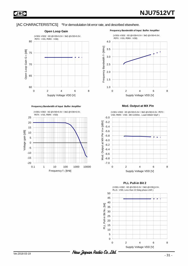
[AC CHARACTERISTICS] *For demodulation bit error rate, and described elsewhere.
Open Loop Gain
60
65
70
75
80
0 2 4 6 8Supply Voltage VDD [V]
Ope
n Lo
op G
ain
G O
[dB]
(VDD1-VDD2 : 0Ω @VDD<5.5V / 3kΩ @VDD>5.5V, PDTX : VSS, PDRX : VDD)
Frequency Bandwidth of Input Buffer Amplifier
1.0
1.5
2.0
2.5
3.0
3.5
4.0
0 2 4 6 8Supply Voltage VDD [V]
Freq
uenc
y Ba
ndw
idth
f T [
MH
z]
(VDD1-VDD2 : 0Ω @VDD<5.5V / 3kΩ @VDD>5.5V, PDTX : VSS, PDRX : VDD)
Frequency Bandwidth of Input Buffer Amplifier
-20
-15
-10
-5
0
5
10
15
20
25
0.1 1 10 100 1000 10000Frequency f T [kHz]
Volta
ge g
ain
[dB]
(VDD1-VDD2 : 0Ω @VDD<5.5V / 3kΩ @VDD>5.5V, PDTX : VSS, PDRX : VDD)
PLL Pull-in Bit 2
0
5
10
15
20
25
30
35
40
45
50
0 2 4 6 8Supply Voltage VDD [V]
PLL
Pull-
in B
it NL
L [bi
t]
(VDD1-VDD2 : 0Ω @VDD<5.5V / 3kΩ @VDD>5.5V,PLLS : VDD, Less than 22.5deg phase shif t )
Mod. Output at MX Pin
-7.0
-6.8
-6.6
-6.4
-6.2
-6.0
-5.8
-5.6
-5.4
-5.2
-5.0
0 2 4 6 8Supply Voltage VDD [V]
Mod
. Out
put a
t MX
Pin
V OM [d
BV]
(VDD1-VDD2 : 0Ω @VDD<5.5V / 3kΩ @VDD>5.5V, PDTX :VDD, PDRX : VDD , MX=1200Hz , Load=30kΩ// 50pF )
NJU7512VT
Ver.2018-03-19 - 32 -
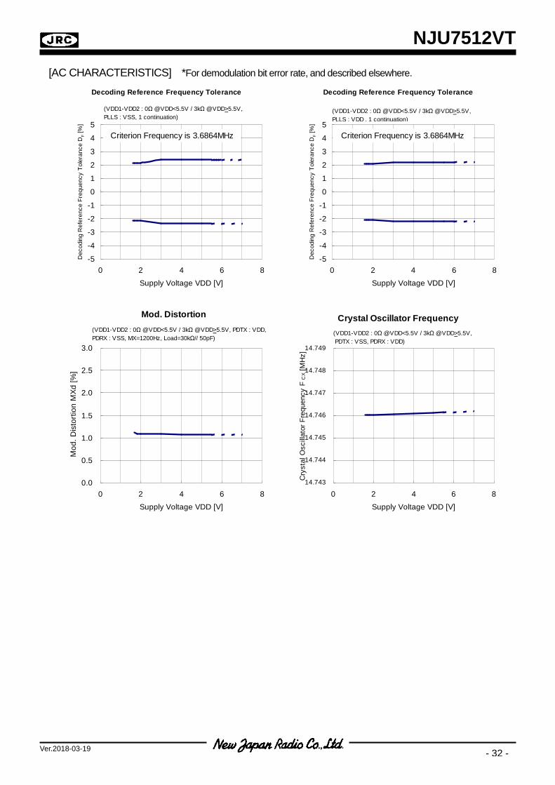
[AC CHARACTERISTICS] *For demodulation bit error rate, and described elsewhere.
Decoding Reference Frequency Tolerance
-5
-4
-3
-2
-1
0
1
2
3
4
5
0 2 4 6 8Supply Voltage VDD [V]
Dec
odin
g R
efer
ence
Fre
quen
cy T
oler
ance
D F [%
]
(VDD1-VDD2 : 0Ω @VDD<5.5V / 3kΩ @VDD>5.5V,PLLS : VSS, 1 continuation)
Criterion Frequency is 3.6864MHz
Decoding Reference Frequency Tolerance
-5
-4
-3
-2
-1
0
1
2
3
4
5
0 2 4 6 8Supply Voltage VDD [V]
Dec
odin
g R
efer
ence
Fre
quen
cy T
oler
ance
D F [%
]
(VDD1-VDD2 : 0Ω @VDD<5.5V / 3kΩ @VDD>5.5V,PLLS : VDD , 1 continuation)
Criterion Frequency is 3.6864MHz
Crystal Oscillator Frequency
14.743
14.744
14.745
14.746
14.747
14.748
14.749
0 2 4 6 8Supply Voltage VDD [V]
Cry
stal
Osc
illat
or F
requ
ency
F C
X [M
Hz]
(VDD1-VDD2 : 0Ω @VDD<5.5V / 3kΩ @VDD>5.5V, PDTX : VSS, PDRX : VDD)
Mod. Distortion
0.0
0.5
1.0
1.5
2.0
2.5
3.0
0 2 4 6 8Supply Voltage VDD [V]
Mod
. Dis
torti
on M
Xd [%
]
(VDD1-VDD2 : 0Ω @VDD<5.5V / 3kΩ @VDD>5.5V, PDTX : VDD,PDRX : VSS, MX=1200Hz, Load=30kΩ// 50pF)
NJU7512VT
Ver.2018-03-19 - 33 -
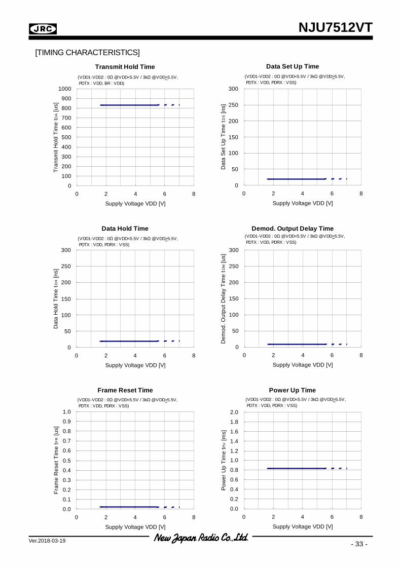
[TIMING CHARACTERISTICS]
Transmit Hold Time
0
100
200
300
400
500
600
700
800
900
1000
0 2 4 6 8
Supply Voltage VDD [V]
Tran
smit
Hol
d Ti
me
t DA
[us]
(VDD1-VDD2 : 0Ω @VDD<5.5V / 3kΩ @VDD>5.5V, PDTX : VDD, BR : VDD)
Data Set Up Time
0
50
100
150
200
250
300
0 2 4 6 8
Supply Voltage VDD [V]
Dat
a Se
t Up
Tim
e t D
S [n
s]
(VDD1-VDD2 : 0Ω @VDD<5.5V / 3kΩ @VDD>5.5V, PDTX : VDD, PDRX : VSS)
Data Hold Time
0
50
100
150
200
250
300
0 2 4 6 8
Supply Voltage VDD [V]
Dat
a H
old
Tim
e t D
H [n
s]
(VDD1-VDD2 : 0Ω @VDD<5.5V / 3kΩ @VDD>5.5V, PDTX : VDD, PDRX : VSS)
Demod. Output Delay Time
0
50
100
150
200
250
300
0 2 4 6 8
Supply Voltage VDD [V]
Dem
od. O
utpu
t Del
ay T
ime
t OM [u
s]
(VDD1-VDD2 : 0Ω @VDD<5.5V / 3kΩ @VDD>5.5V, PDTX : VDD, PDRX : VSS)
Frame Reset Time
0.0
0.1
0.2
0.3
0.4
0.5
0.6
0.7
0.8
0.9
1.0
0 2 4 6 8
Supply Voltage VDD [V]
Fram
e R
eset
Tim
e t F
R [u
s]
(VDD1-VDD2 : 0Ω @VDD<5.5V / 3kΩ @VDD>5.5V, PDTX : VDD, PDRX : VSS)
Power Up Time
0.0
0.2
0.4
0.6
0.8
1.01.2
1.4
1.6
1.8
2.0
0 2 4 6 8
Supply Voltage VDD [V]
Pow
er U
p Ti
me
t PU [m
s]
(VDD1-VDD2 : 0Ω @VDD<5.5V / 3kΩ @VDD>5.5V, PDTX : VDD, PDRX : VSS)
NJU7512VT
Ver.2018-03-19 - 34 -
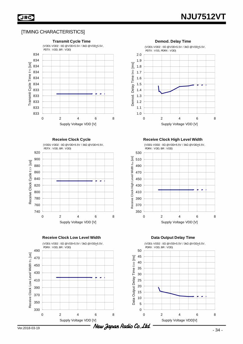
[TIMING CHARACTERISTICS]
Transmit Cycle Time
833
833
833
833
833
834
834
834
834
834
834
0 2 4 6 8Supply Voltage VDD [V]
Tran
smit
Cyc
le T
ime
t TC
[us]
(VDD1-VDD2 : 0Ω @VDD<5.5V / 3kΩ @VDD>5.5V, PDTX : VDD, BR : VDD)
Demod. Delay Time
1.0
1.1
1.2
1.3
1.4
1.5
1.6
1.7
1.8
1.9
2.0
0 2 4 6 8Supply Voltage VDD [V]
Dem
od. D
elay
Tim
e t R
D [m
s]
(VDD1-VDD2 : 0Ω @VDD<5.5V / 3kΩ @VDD>5.5V, PDTX : VSS, PDRX : VDD)
Receive Clock Cycle
740
760
780
800
820
840
860
880
900
920
0 2 4 6 8Supply Voltage VDD [V]
Rec
eive
Clo
ck C
ycle
t C
Y [u
s]
(VDD1-VDD2 : 0Ω @VDD<5.5V / 3kΩ @VDD>5.5V, PDTX : VDD, BR : VDD)
Receive Clock High Level Width
350
370
390
410
430
450
470
490
510
530
0 2 4 6 8Supply Voltage VDD [V]
Rec
eive
Clo
ck H
igh
Leve
l Wid
th t T
H [u
s]
(VDD1-VDD2 : 0Ω @VDD<5.5V / 3kΩ @VDD>5.5V, PDRX : VDD, BR : VDD)
Receive Clock Low Level Width
330
350
370
390
410
430
450
470
490
0 2 4 6 8Supply Voltage VDD [V]
Rec
eive
Clo
ck L
ow L
evel
Wid
th t T
L [us
]
(VDD1-VDD2 : 0Ω @VDD<5.5V / 3kΩ @VDD>5.5V, PDRX : VDD, BR : VDD)
Data Output Delay Time
0
5
10
15
20
25
30
35
40
45
50
0 2 4 6 8Supply Voltage VDD[V]
Dat
a O
utpu
t Del
ay T
ime
t DD [n
s]
(VDD1-VDD2 : 0Ω @VDD<5.5V / 3kΩ @VDD>5.5V, PDRX : VDD, BR : VDD)
NJU7512VT
Ver.2018-03-19 - 35 -
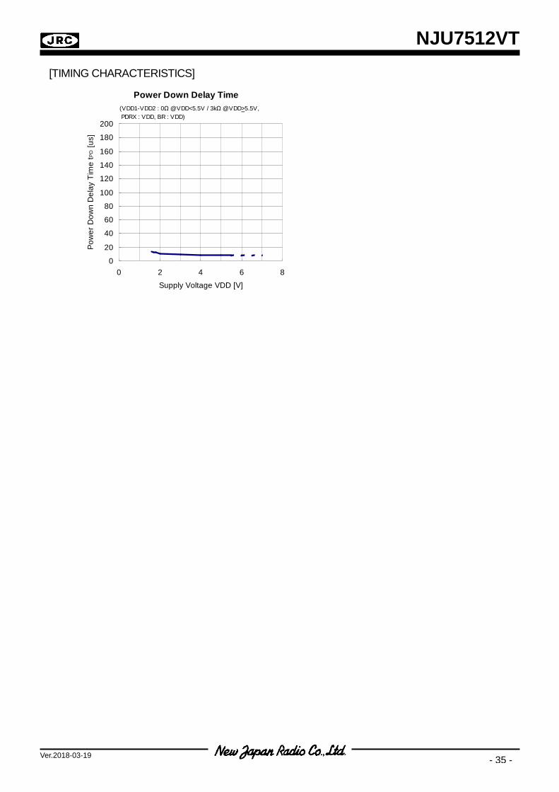
[TIMING CHARACTERISTICS]
Power Down Delay Time
0
20
40
60
80
100
120
140
160
180
200
0 2 4 6 8Supply Voltage VDD [V]
Pow
er D
own
Del
ay T
ime
t PD [u
s]
(VDD1-VDD2 : 0Ω @VDD<5.5V / 3kΩ @VDD>5.5V, PDRX : VDD, BR : VDD)
NJU7512VT
Ver.2018-03-19 - 36 -
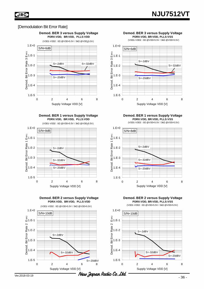
[Demodulation Bit Error Rate]
Demod. BER 3 versus Supply VoltagePDRX:VDD, BR:VDD, PLLS:VDD
1.E-5
1.E-4
1.E-3
1.E-2
1.E-1
1.E+0
0 2 4 6 8Supply Voltage VDD [V]
Dem
od. B
it Er
ror R
ate
3 E
BR3
(VDD1-VDD2 : 0Ω @VDD<5.5V / 3kΩ @VDD>5.5V)
S/N=6dB
S=-2dBV S=-32dBV
S=-20dBV
Demod. BER 3 versus Supply VoltagePDRX:VDD, BR:VDD, PLLS:VSS
1.E-5
1.E-4
1.E-3
1.E-2
1.E-1
1.E+0
0 2 4 6 8Supply Voltage VDD [V]
Dem
od. B
it Er
ror R
ate
3 E
BR3
(VDD1-VDD2 : 0Ω @VDD<5.5V / 3kΩ @VDD>5.5V)
S/N=6dB
S=-2dBV
S=-20dBV
S=-32dBV
Demod. BER 1 versus Supply VoltagePDRX:VDD, BR:VDD, PLLS:VDD
1.E-5
1.E-4
1.E-3
1.E-2
1.E-1
1.E+0
0 2 4 6 8Supply Voltage VDD [V]
Dem
od. B
it Er
ror R
ate
1 E
BR1
S/N=8dB
S=-2dBV
S=-32dBV
S=-20dBV
(VDD1-VDD2 : 0Ω @VDD<5.5V / 3kΩ @VDD>5.5V)
Demod. BER 2 versus Supply VoltagePDRX:VDD, BR:VDD, PLLS:VDD
1.E-5
1.E-4
1.E-3
1.E-2
1.E-1
1.E+0
0 2 4 6 8Supply Voltage VDD [V]
Dem
od. B
it Er
ror R
ate
2 E
BR
2
S/N=10dB
S=-2dBV
S=-20dBV
(VDD1-VDD2 : 0Ω @VDD<5.5V / 3kΩ @VDD>5.5V)
S=-32dBV
Demod. BER 1 versus Supply VoltagePDRX:VDD, BR:VDD, PLLS:VSS
1.E-5
1.E-4
1.E-3
1.E-2
1.E-1
1.E+0
0 2 4 6 8Supply Voltage VDD [V]
Dem
od. B
it Er
ror R
ate
1 E
BR1
(VDD1-VDD2 : 0Ω @VDD<5.5V / 3kΩ @VDD>5.5V)
S/N=8dB
S=-2dBV
S=-32dBV
S=-20dBV
Demod. BER 2 versus Supply VoltagePDRX:VDD, BR:VDD, PLLS:VSS
1.E-5
1.E-4
1.E-3
1.E-2
1.E-1
1.E+0
0 2 4 6 8Supply Voltage VDD [V]
Dem
od. B
it Er
ror R
ate
2 E
BR
2
(VDD1-VDD2 : 0Ω @VDD<5.5V / 3kΩ @VDD>5.5V)
S/N=10dB
S=-2dBV
S=-32dBVS=-20dBV
NJU7512VT
Ver.2018-03-19 - 37 -
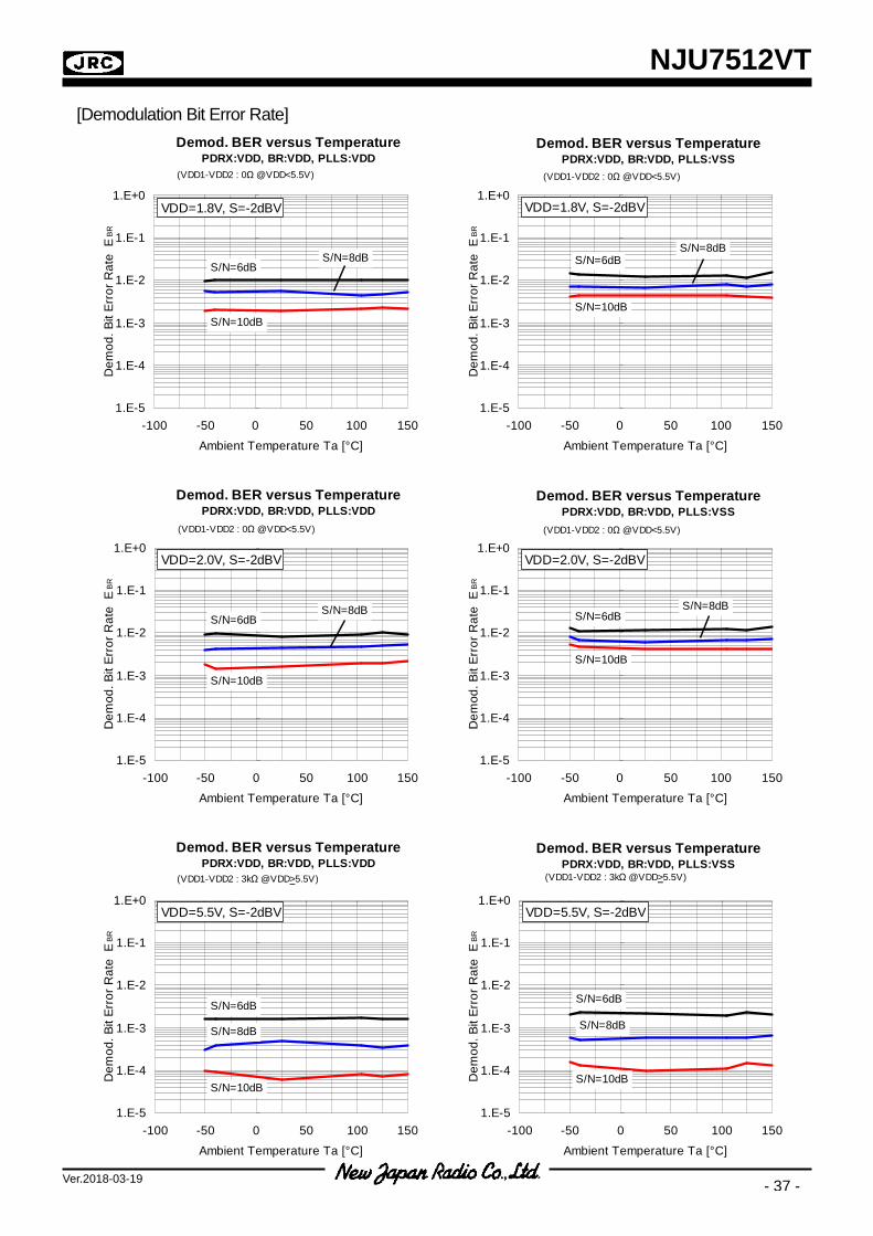
[Demodulation Bit Error Rate]
Demod. BER versus TemperaturePDRX:VDD, BR:VDD, PLLS:VDD
1.E-5
1.E-4
1.E-3
1.E-2
1.E-1
1.E+0
-100 -50 0 50 100 150Ambient Temperature Ta [°C]
Dem
od. B
it Er
ror R
ate
E B
R
S/N=8dB
S/N=10dB
S/N=6dB
(VDD1-VDD2 : 0Ω @VDD<5.5V)
VDD=1.8V, S=-2dBV
Demod. BER versus TemperaturePDRX:VDD, BR:VDD, PLLS:VSS
1.E-5
1.E-4
1.E-3
1.E-2
1.E-1
1.E+0
-100 -50 0 50 100 150Ambient Temperature Ta [°C]
Dem
od. B
it Er
ror R
ate
E B
R
VDD=1.8V, S=-2dBV
(VDD1-VDD2 : 0Ω @VDD<5.5V)
S/N=8dB
S/N=10dB
S/N=6dB
Demod. BER versus TemperaturePDRX:VDD, BR:VDD, PLLS:VDD
1.E-5
1.E-4
1.E-3
1.E-2
1.E-1
1.E+0
-100 -50 0 50 100 150Ambient Temperature Ta [°C]
Dem
od. B
it Er
ror R
ate
E B
R
S/N=8dB
S/N=10dB
S/N=6dB
(VDD1-VDD2 : 0Ω @VDD<5.5V)
VDD=2.0V, S=-2dBV
Demod. BER versus TemperaturePDRX:VDD, BR:VDD, PLLS:VDD
1.E-5
1.E-4
1.E-3
1.E-2
1.E-1
1.E+0
-100 -50 0 50 100 150Ambient Temperature Ta [°C]
Dem
od. B
it Er
ror R
ate
E B
R
S/N=6dB
(VDD1-VDD2 : 3kΩ @VDD>5.5V)
S/N=8dB
S/N=10dB
VDD=5.5V, S=-2dBV
Demod. BER versus TemperaturePDRX:VDD, BR:VDD, PLLS:VSS
1.E-5
1.E-4
1.E-3
1.E-2
1.E-1
1.E+0
-100 -50 0 50 100 150Ambient Temperature Ta [°C]
Dem
od. B
it Er
ror R
ate
E B
R
VDD=2.0V, S=-2dBV
(VDD1-VDD2 : 0Ω @VDD<5.5V)
S/N=8dB
S/N=10dB
S/N=6dB
Demod. BER versus TemperaturePDRX:VDD, BR:VDD, PLLS:VSS
1.E-5
1.E-4
1.E-3
1.E-2
1.E-1
1.E+0
-100 -50 0 50 100 150Ambient Temperature Ta [°C]
Dem
od. B
it Er
ror R
ate
E B
R
VDD=5.5V, S=-2dBV
(VDD1-VDD2 : 3kΩ @VDD>5.5V)
S/N=6dB
S/N=10dB
S/N=8dB
NJU7512VT
Ver.2018-03-19 - 38 -
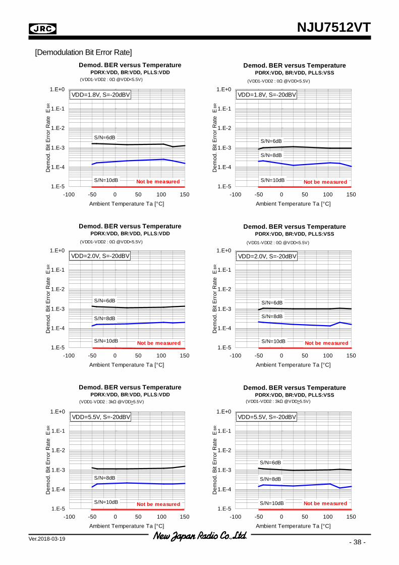
[Demodulation Bit Error Rate]
Demod. BER versus TemperaturePDRX:VDD, BR:VDD, PLLS:VDD
1.E-5
1.E-4
1.E-3
1.E-2
1.E-1
1.E+0
-100 -50 0 50 100 150Ambient Temperature Ta [°C]
Dem
od. B
it Er
ror R
ate
E B
R
S/N=10dB
S/N=6dB
(VDD1-VDD2 : 0Ω @VDD<5.5V)
VDD=1.8V, S=-20dBV
Not be measured
Demod. BER versus TemperaturePDRX:VDD, BR:VDD, PLLS:VDD
1.E-5
1.E-4
1.E-3
1.E-2
1.E-1
1.E+0
-100 -50 0 50 100 150Ambient Temperature Ta [°C]
Dem
od. B
it Er
ror R
ate
E B
R
S/N=8dB
S/N=6dB
(VDD1-VDD2 : 0Ω @VDD<5.5V)
VDD=2.0V, S=-20dBV
S/N=10dB Not be measured
Demod. BER versus TemperaturePDRX:VDD, BR:VDD, PLLS:VDD
1.E-5
1.E-4
1.E-3
1.E-2
1.E-1
1.E+0
-100 -50 0 50 100 150Ambient Temperature Ta [°C]
Dem
od. B
it Er
ror R
ate
E B
R
(VDD1-VDD2 : 3kΩ @VDD>5.5V)
S/N=8dB
S/N=10dB
VDD=5.5V, S=-20dBV
Not be measured
Demod. BER versus TemperaturePDRX:VDD, BR:VDD, PLLS:VSS
1.E-5
1.E-4
1.E-3
1.E-2
1.E-1
1.E+0
-100 -50 0 50 100 150Ambient Temperature Ta [°C]
Dem
od. B
it Er
ror R
ate
E B
R
VDD=1.8V, S=-20dBV
(VDD1-VDD2 : 0Ω @VDD<5.5V)
S/N=8dB
S/N=10dB
S/N=6dB
Not be measured
Demod. BER versus TemperaturePDRX:VDD, BR:VDD, PLLS:VSS
1.E-5
1.E-4
1.E-3
1.E-2
1.E-1
1.E+0
-100 -50 0 50 100 150Ambient Temperature Ta [°C]
Dem
od. B
it Er
ror R
ate
E B
R
VDD=2.0V, S=-20dBV
(VDD1-VDD2 : 0Ω @VDD<5.5V)
S/N=8dB
S/N=10dB
S/N=6dB
Not be measured
Demod. BER versus TemperaturePDRX:VDD, BR:VDD, PLLS:VSS
1.E-5
1.E-4
1.E-3
1.E-2
1.E-1
1.E+0
-100 -50 0 50 100 150Ambient Temperature Ta [°C]
Dem
od. B
it Er
ror R
ate
E B
R
VDD=5.5V, S=-20dBV
(VDD1-VDD2 : 3kΩ @VDD>5.5V)
S/N=6dB
S/N=10dB
S/N=8dB
Not be measured
NJU7512VT
Ver.2018-03-19 - 39 -
[Demodulation Bit Error Rate]
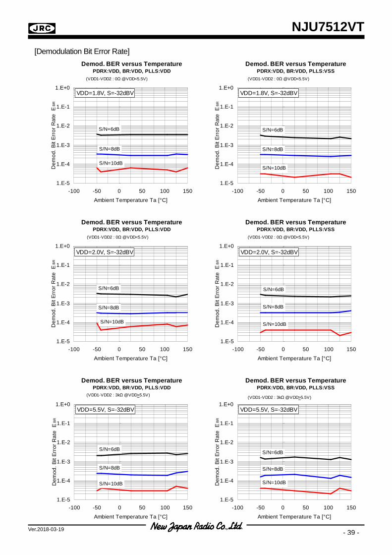
Demod. BER versus TemperaturePDRX:VDD, BR:VDD, PLLS:VDD
1.E-5
1.E-4
1.E-3
1.E-2
1.E-1
1.E+0
-100 -50 0 50 100 150Ambient Temperature Ta [°C]
Dem
od. B
it Er
ror R
ate
E B
R
(VDD1-VDD2 : 0Ω @VDD<5.5V)
VDD=1.8V, S=-32dBV
S/N=6dB
S/N=10dB
S/N=8dB
Demod. BER versus TemperaturePDRX:VDD, BR:VDD, PLLS:VSS
1.E-5
1.E-4
1.E-3
1.E-2
1.E-1
1.E+0
-100 -50 0 50 100 150Ambient Temperature Ta [°C]
Dem
od. B
it Er
ror R
ate
E B
R
(VDD1-VDD2 : 0Ω @VDD<5.5V)
VDD=1.8V, S=-32dBV
S/N=6dB
S/N=10dB
S/N=8dB
Demod. BER versus TemperaturePDRX:VDD, BR:VDD, PLLS:VDD
1.E-5
1.E-4
1.E-3
1.E-2
1.E-1
1.E+0
-100 -50 0 50 100 150Ambient Temperature Ta [°C]
Dem
od. B
it Er
ror R
ate
E B
R
(VDD1-VDD2 : 0Ω @VDD<5.5V)
VDD=2.0V, S=-32dBV
S/N=6dB
S/N=10dB
S/N=8dB
Demod. BER versus TemperaturePDRX:VDD, BR:VDD, PLLS:VDD
1.E-5
1.E-4
1.E-3
1.E-2
1.E-1
1.E+0
-100 -50 0 50 100 150Ambient Temperature Ta [°C]
Dem
od. B
it Er
ror R
ate
E B
R
VDD=5.5V, S=-32dBV
(VDD1-VDD2 : 3kΩ @VDD>5.5V)
S/N=6dB
S/N=10dB
S/N=8dB
Demod. BER versus TemperaturePDRX:VDD, BR:VDD, PLLS:VSS
1.E-5
1.E-4
1.E-3
1.E-2
1.E-1
1.E+0
-100 -50 0 50 100 150Ambient Temperature Ta [°C]
Dem
od. B
it Er
ror R
ate
E B
R
(VDD1-VDD2 : 0Ω @VDD<5.5V)
VDD=2.0V, S=-32dBV
S/N=6dB
S/N=10dB
S/N=8dB
Demod. BER versus TemperaturePDRX:VDD, BR:VDD, PLLS:VSS
1.E-5
1.E-4
1.E-3
1.E-2
1.E-1
1.E+0
-100 -50 0 50 100 150Ambient Temperature Ta [°C]
Dem
od. B
it Er
ror R
ate
E B
R
VDD=5.5V, S=-32dBV
(VDD1-VDD2 : 3kΩ @VDD>5.5V)
S/N=6dB
S/N=10dB
S/N=8dB
NJU7512VT
Ver.2018-03-19 - 40 -
[Demodulation Bit Error Rate]
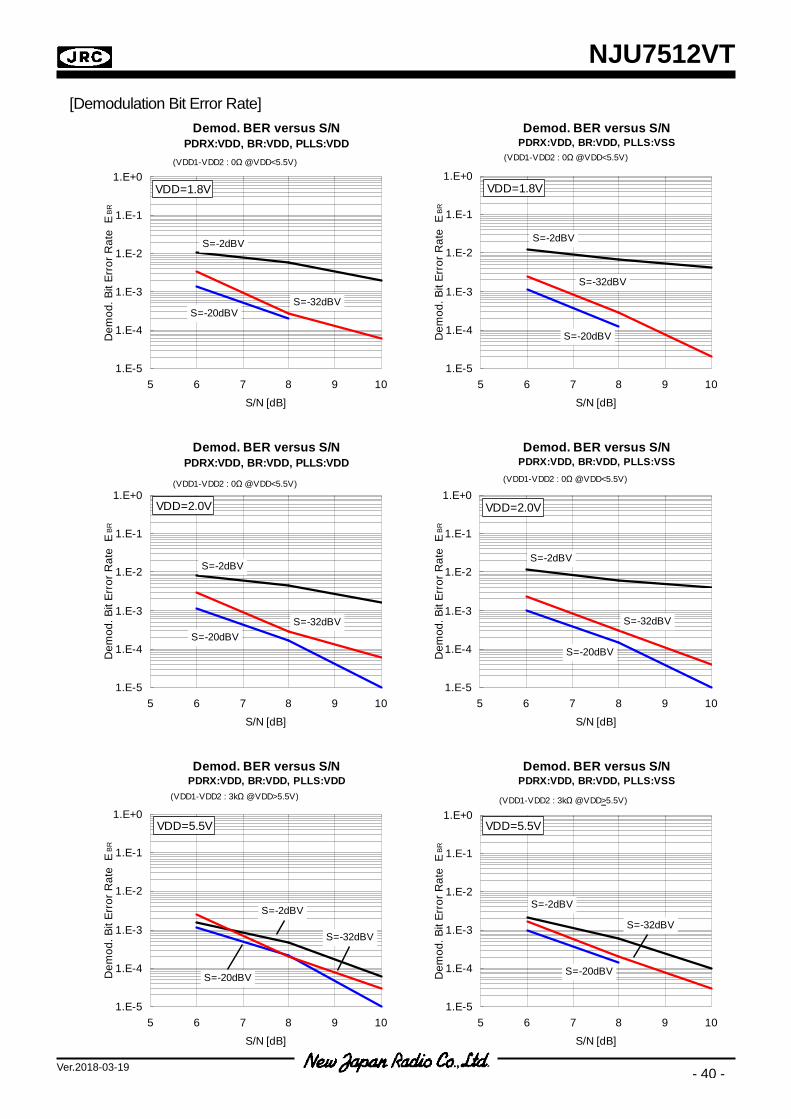
Demod. BER versus S/NPDRX:VDD, BR:VDD, PLLS:VDD
1.E-5
1.E-4
1.E-3
1.E-2
1.E-1
1.E+0
5 6 7 8 9 10S/N [dB]
Dem
od. B
it Er
ror R
ate
E B
R
VDD=1.8V
S=-2dBV
S=-32dBVS=-20dBV
(VDD1-VDD2 : 0Ω @VDD<5.5V)
Demod. BER versus S/NPDRX:VDD, BR:VDD, PLLS:VSS
1.E-5
1.E-4
1.E-3
1.E-2
1.E-1
1.E+0
5 6 7 8 9 10S/N [dB]
Dem
od. B
it Er
ror R
ate
E B
R
VDD=1.8V
S=-2dBV
S=-32dBV
S=-20dBV
(VDD1-VDD2 : 0Ω @VDD<5.5V)
Demod. BER versus S/NPDRX:VDD, BR:VDD, PLLS:VDD
1.E-5
1.E-4
1.E-3
1.E-2
1.E-1
1.E+0
5 6 7 8 9 10S/N [dB]
Dem
od. B
it Er
ror R
ate
E B
R
VDD=2.0V
S=-2dBV
S=-32dBVS=-20dBV
(VDD1-VDD2 : 0Ω @VDD<5.5V)
Demod. BER versus S/NPDRX:VDD, BR:VDD, PLLS:VDD
1.E-5
1.E-4
1.E-3
1.E-2
1.E-1
1.E+0
5 6 7 8 9 10S/N [dB]
Dem
od. B
it Er
ror R
ate
E B
R
VDD=5.5V
S=-2dBV
S=-32dBV
S=-20dBV
(VDD1-VDD2 : 3kΩ @VDD>5.5V)
Demod. BER versus S/NPDRX:VDD, BR:VDD, PLLS:VSS
1.E-5
1.E-4
1.E-3
1.E-2
1.E-1
1.E+0
5 6 7 8 9 10S/N [dB]
Dem
od. B
it Er
ror R
ate
E B
R
VDD=2.0V
S=-2dBV
S=-32dBV
S=-20dBV
(VDD1-VDD2 : 0Ω @VDD<5.5V)
Demod. BER versus S/NPDRX:VDD, BR:VDD, PLLS:VSS
1.E-5
1.E-4
1.E-3
1.E-2
1.E-1
1.E+0
5 6 7 8 9 10S/N [dB]
Dem
od. B
it Er
ror R
ate
E B
R
VDD=5.5V
S=-2dBV
S=-32dBV
S=-20dBV
(VDD1-VDD2 : 3kΩ @VDD>5.5V)
NJU7512VT
Ver.2018-03-19 - 41 -
[Demodulation Bit Error Rate]
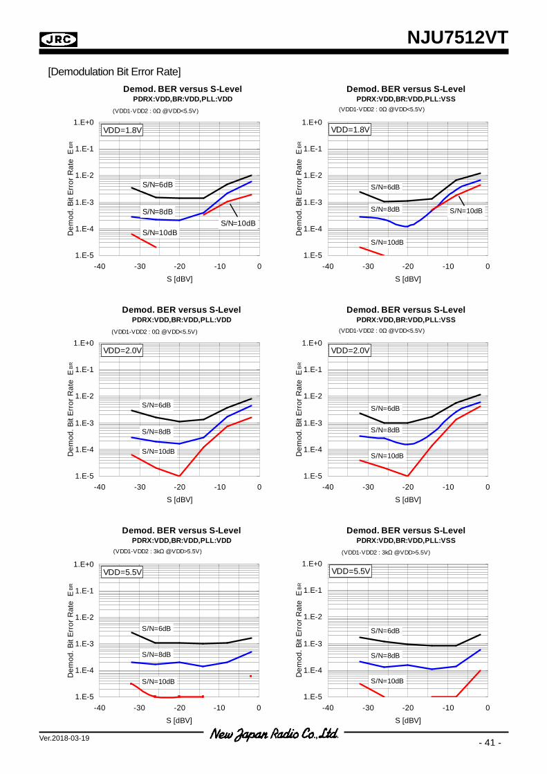
Demod. BER versus S-LevelPDRX:VDD,BR:VDD,PLL:VDD
1.E-5
1.E-4
1.E-3
1.E-2
1.E-1
1.E+0
-40 -30 -20 -10 0S [dBV]
Dem
od. B
it Er
ror R
ate
E B
R
VDD=1.8V
(VDD1-VDD2 : 0Ω @VDD<5.5V)
S/N=8dBS/N=10dB
S/N=6dB
S/N=10dB
Demod. BER versus S-LevelPDRX:VDD,BR:VDD,PLL:VSS
1.E-5
1.E-4
1.E-3
1.E-2
1.E-1
1.E+0
-40 -30 -20 -10 0S [dBV]
Dem
od. B
it Er
ror R
ate
E B
R
VDD=1.8V
(VDD1-VDD2 : 0Ω @VDD<5.5V)
S/N=8dB
S/N=6dB
S/N=10dB
S/N=10dB
Demod. BER versus S-LevelPDRX:VDD,BR:VDD,PLL:VDD
1.E-5
1.E-4
1.E-3
1.E-2
1.E-1
1.E+0
-40 -30 -20 -10 0S [dBV]
Dem
od. B
it Er
ror R
ate
E B
R
VDD=2.0V
(VDD1-VDD2 : 0Ω @VDD<5.5V)
S/N=8dB
S/N=10dB
S/N=6dB
Demod. BER versus S-LevelPDRX:VDD,BR:VDD,PLL:VDD
1.E-5
1.E-4
1.E-3
1.E-2
1.E-1
1.E+0
-40 -30 -20 -10 0S [dBV]
Dem
od. B
it Er
ror R
ate
E B
R
S/N=8dB
S/N=10dB
S/N=6dB
(VDD1-VDD2 : 3kΩ @VDD>5.5V)
VDD=5.5V
Demod. BER versus S-LevelPDRX:VDD,BR:VDD,PLL:VSS
1.E-5
1.E-4
1.E-3
1.E-2
1.E-1
1.E+0
-40 -30 -20 -10 0S [dBV]
Dem
od. B
it Er
ror R
ate
E B
R
VDD=2.0V
(VDD1-VDD2 : 0Ω @VDD<5.5V)
S/N=8dB
S/N=6dB
S/N=10dB
Demod. BER versus S-LevelPDRX:VDD,BR:VDD,PLL:VSS
1.E-5
1.E-4
1.E-3
1.E-2
1.E-1
1.E+0
-40 -30 -20 -10 0S [dBV]
Dem
od. B
it Er
ror R
ate
E B
R
VDD=5.5V
S/N=8dB
S/N=6dB
S/N=10dB
(VDD1-VDD2 : 3kΩ @VDD>5.5V)
NJU7512VT
Ver.2018-03-19 - 42 -
[CAUTION] The specifications on this databook are only
given for information , without any guarantee as regards either mistakes or omissions. The application circuits in this databook are described only to show representative usages of the product and not intended for the guarantee or permission of any right including the industrial rights.