Embed Size (px)
Citation preview
July 2008 Rev 22 1/38
38
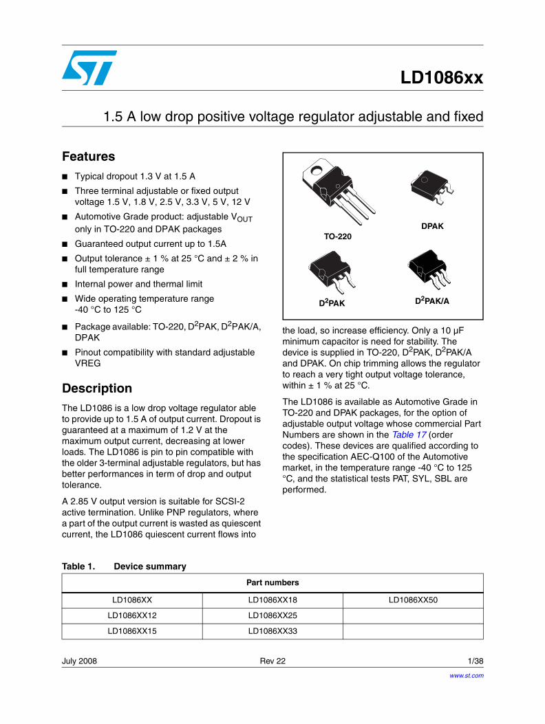
LD1086xx
1.5 A low drop positive voltage regulator adjustable and fixed
Features■ Typical dropout 1.3 V at 1.5 A
■ Three terminal adjustable or fixed output voltage 1.5 V, 1.8 V, 2.5 V, 3.3 V, 5 V, 12 V
■ Automotive Grade product: adjustable VOUT only in TO-220 and DPAK packages
■ Guaranteed output current up to 1.5A
■ Output tolerance ± 1 % at 25 °C and ± 2 % in full temperature range
■ Internal power and thermal limit
■ Wide operating temperature range -40 °C to 125 °C
■ Package available: TO-220, D2PAK, D2PAK/A, DPAK
■ Pinout compatibility with standard adjustable VREG
DescriptionThe LD1086 is a low drop voltage regulator able to provide up to 1.5 A of output current. Dropout is guaranteed at a maximum of 1.2 V at the maximum output current, decreasing at lower loads. The LD1086 is pin to pin compatible with the older 3-terminal adjustable regulators, but has better performances in term of drop and output tolerance.
A 2.85 V output version is suitable for SCSI-2 active termination. Unlike PNP regulators, where a part of the output current is wasted as quiescent current, the LD1086 quiescent current flows into
the load, so increase efficiency. Only a 10 µF minimum capacitor is need for stability. The device is supplied in TO-220, D2PAK, D2PAK/A and DPAK. On chip trimming allows the regulator to reach a very tight output voltage tolerance, within ± 1 % at 25 °C.
The LD1086 is available as Automotive Grade in TO-220 and DPAK packages, for the option of adjustable output voltage whose commercial Part Numbers are shown in the Table 17 (order codes). These devices are qualified according to the specification AEC-Q100 of the Automotive market, in the temperature range -40 °C to 125 °C, and the statistical tests PAT, SYL, SBL are performed.
DPAK
D2PAK/A
TO-220
D2PAK
Table 1. Device summary
Part numbers
LD1086XX LD1086XX18 LD1086XX50
LD1086XX12 LD1086XX25
LD1086XX15 LD1086XX33
www.st.com
Contents LD1086xx
2/38
Contents
1 Diagram . . . . . . . . . . . . . . . . . . . . . . . . . . . . . . . . . . . . . . . . . . . . . . . . . . . 5
2 Pin configuration . . . . . . . . . . . . . . . . . . . . . . . . . . . . . . . . . . . . . . . . . . . 6
3 Maximum ratings . . . . . . . . . . . . . . . . . . . . . . . . . . . . . . . . . . . . . . . . . . . . 7
4 Schematic application . . . . . . . . . . . . . . . . . . . . . . . . . . . . . . . . . . . . . . . 8
5 Electrical characteristics . . . . . . . . . . . . . . . . . . . . . . . . . . . . . . . . . . . . . 9
6 Typical application . . . . . . . . . . . . . . . . . . . . . . . . . . . . . . . . . . . . . . . . . 18
7 Package mechanical data . . . . . . . . . . . . . . . . . . . . . . . . . . . . . . . . . . . . 23
8 Order codes . . . . . . . . . . . . . . . . . . . . . . . . . . . . . . . . . . . . . . . . . . . . . . 36
9 Revision history . . . . . . . . . . . . . . . . . . . . . . . . . . . . . . . . . . . . . . . . . . . 37
LD1086xx List of figures
3/38
List of figures
Figure 1. Schematic diagram . . . . . . . . . . . . . . . . . . . . . . . . . . . . . . . . . . . . . . . . . . . . . . . . . . . . . . . . 5Figure 2. Pin connections (top view) . . . . . . . . . . . . . . . . . . . . . . . . . . . . . . . . . . . . . . . . . . . . . . . . . . 6Figure 3. Application circuit . . . . . . . . . . . . . . . . . . . . . . . . . . . . . . . . . . . . . . . . . . . . . . . . . . . . . . . . . 8Figure 4. Output voltage vs temperature . . . . . . . . . . . . . . . . . . . . . . . . . . . . . . . . . . . . . . . . . . . . . . 18Figure 5. Output voltage vs temperature . . . . . . . . . . . . . . . . . . . . . . . . . . . . . . . . . . . . . . . . . . . . . . 18Figure 6. Output voltage vs temperature . . . . . . . . . . . . . . . . . . . . . . . . . . . . . . . . . . . . . . . . . . . . . . 18Figure 7. Short circuit current vs dropout voltage . . . . . . . . . . . . . . . . . . . . . . . . . . . . . . . . . . . . . . . 18Figure 8. Line regulation vs temperature . . . . . . . . . . . . . . . . . . . . . . . . . . . . . . . . . . . . . . . . . . . . . . 18Figure 9. Load regulation vs temperature . . . . . . . . . . . . . . . . . . . . . . . . . . . . . . . . . . . . . . . . . . . . . 18Figure 10. Dropout voltage vs temperature . . . . . . . . . . . . . . . . . . . . . . . . . . . . . . . . . . . . . . . . . . . . . 19Figure 11. Dropout voltage vs output current. . . . . . . . . . . . . . . . . . . . . . . . . . . . . . . . . . . . . . . . . . . . 19Figure 12. Adjust pin current vs input voltage . . . . . . . . . . . . . . . . . . . . . . . . . . . . . . . . . . . . . . . . . . . 19Figure 13. Adjust pin current vs temperature. . . . . . . . . . . . . . . . . . . . . . . . . . . . . . . . . . . . . . . . . . . . 19Figure 14. Adjust pin current vs output current . . . . . . . . . . . . . . . . . . . . . . . . . . . . . . . . . . . . . . . . . . 19Figure 15. Quiescent current vs output current . . . . . . . . . . . . . . . . . . . . . . . . . . . . . . . . . . . . . . . . . . 19Figure 16. Quiescent current vs input voltage . . . . . . . . . . . . . . . . . . . . . . . . . . . . . . . . . . . . . . . . . . . 20Figure 17. Supply voltage rejection vs output current . . . . . . . . . . . . . . . . . . . . . . . . . . . . . . . . . . . . . 20Figure 18. Supply voltage rejection vs frequency . . . . . . . . . . . . . . . . . . . . . . . . . . . . . . . . . . . . . . . . 20Figure 19. Supply voltage rejection vs temperature. . . . . . . . . . . . . . . . . . . . . . . . . . . . . . . . . . . . . . . 20Figure 20. Minimum load current vs temperature . . . . . . . . . . . . . . . . . . . . . . . . . . . . . . . . . . . . . . . . 20Figure 21. Stability for adjustable. . . . . . . . . . . . . . . . . . . . . . . . . . . . . . . . . . . . . . . . . . . . . . . . . . . . . 20Figure 22. Stability for 2.85 V. . . . . . . . . . . . . . . . . . . . . . . . . . . . . . . . . . . . . . . . . . . . . . . . . . . . . . . . 21Figure 23. Stability for 12 V . . . . . . . . . . . . . . . . . . . . . . . . . . . . . . . . . . . . . . . . . . . . . . . . . . . . . . . . . 21Figure 24. Line transient . . . . . . . . . . . . . . . . . . . . . . . . . . . . . . . . . . . . . . . . . . . . . . . . . . . . . . . . . . . 21Figure 25. Line transient . . . . . . . . . . . . . . . . . . . . . . . . . . . . . . . . . . . . . . . . . . . . . . . . . . . . . . . . . . . 21Figure 26. Line transient . . . . . . . . . . . . . . . . . . . . . . . . . . . . . . . . . . . . . . . . . . . . . . . . . . . . . . . . . . . 21Figure 27. Load transient . . . . . . . . . . . . . . . . . . . . . . . . . . . . . . . . . . . . . . . . . . . . . . . . . . . . . . . . . . . 21Figure 28. Load transient . . . . . . . . . . . . . . . . . . . . . . . . . . . . . . . . . . . . . . . . . . . . . . . . . . . . . . . . . . . 22Figure 29. Thermal protection . . . . . . . . . . . . . . . . . . . . . . . . . . . . . . . . . . . . . . . . . . . . . . . . . . . . . . . 22Figure 30. Drawing dimension D²PAK (type STD-ST) . . . . . . . . . . . . . . . . . . . . . . . . . . . . . . . . . . . . . 26Figure 31. Drawing dimension D²PAK (type WOOSEOK-SUBCON.) . . . . . . . . . . . . . . . . . . . . . . . . . 27Figure 32. D²PAK footprint recommended data. . . . . . . . . . . . . . . . . . . . . . . . . . . . . . . . . . . . . . . . . . 29Figure 33. Drawing dimension D²PAK/A (type STD-ST) . . . . . . . . . . . . . . . . . . . . . . . . . . . . . . . . . . . 30Figure 34. Drawing dimension D²PAK/A (type WOOSEOK-Subcon.) . . . . . . . . . . . . . . . . . . . . . . . . . 31Figure 35. D²PAK/A footprint recommended data . . . . . . . . . . . . . . . . . . . . . . . . . . . . . . . . . . . . . . . . 33
List of tables LD1086xx
4/38
List of tables
Table 1. Device summary . . . . . . . . . . . . . . . . . . . . . . . . . . . . . . . . . . . . . . . . . . . . . . . . . . . . . . . . . . 1Table 2. Absolute maximum ratings . . . . . . . . . . . . . . . . . . . . . . . . . . . . . . . . . . . . . . . . . . . . . . . . . . 7Table 3. Thermal data. . . . . . . . . . . . . . . . . . . . . . . . . . . . . . . . . . . . . . . . . . . . . . . . . . . . . . . . . . . . . 7Table 4. Electrical characteristics of LD1086#15 . . . . . . . . . . . . . . . . . . . . . . . . . . . . . . . . . . . . . . . . 9Table 5. Electrical characteristics of LD1086#18 . . . . . . . . . . . . . . . . . . . . . . . . . . . . . . . . . . . . . . . 10Table 6. Electrical characteristics of LD1086#25 . . . . . . . . . . . . . . . . . . . . . . . . . . . . . . . . . . . . . . . 11Table 7. Electrical characteristics of LD1086#33 . . . . . . . . . . . . . . . . . . . . . . . . . . . . . . . . . . . . . . . 12Table 8. Electrical characteristics of LD1086#36 . . . . . . . . . . . . . . . . . . . . . . . . . . . . . . . . . . . . . . . 13Table 9. Electrical characteristics of LD1086#50 . . . . . . . . . . . . . . . . . . . . . . . . . . . . . . . . . . . . . . . 14Table 10. Electrical characteristics of LD1086#12 . . . . . . . . . . . . . . . . . . . . . . . . . . . . . . . . . . . . . . . 15Table 11. Electrical characteristics of LD1086#.. . . . . . . . . . . . . . . . . . . . . . . . . . . . . . . . . . . . . . . . . 16Table 12. Electrical characteristics of LD1086DTTRY and LD1086VY (Automotive Grade) . . . . . . . 17Table 13. D²PAK mechanical data . . . . . . . . . . . . . . . . . . . . . . . . . . . . . . . . . . . . . . . . . . . . . . . . . . . 28Table 14. Footprint data . . . . . . . . . . . . . . . . . . . . . . . . . . . . . . . . . . . . . . . . . . . . . . . . . . . . . . . . . . . 29Table 15. D²PAK/A mechanical data . . . . . . . . . . . . . . . . . . . . . . . . . . . . . . . . . . . . . . . . . . . . . . . . . 32Table 16. Footprint data . . . . . . . . . . . . . . . . . . . . . . . . . . . . . . . . . . . . . . . . . . . . . . . . . . . . . . . . . . . 33Table 17. Order codes . . . . . . . . . . . . . . . . . . . . . . . . . . . . . . . . . . . . . . . . . . . . . . . . . . . . . . . . . . . . 36Table 18. Document revision history . . . . . . . . . . . . . . . . . . . . . . . . . . . . . . . . . . . . . . . . . . . . . . . . . 37
LD1086xx Diagram
5/38
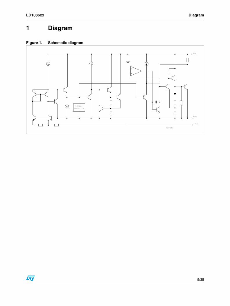
1 Diagram
Figure 1. Schematic diagram
Pin configuration LD1086xx
6/38
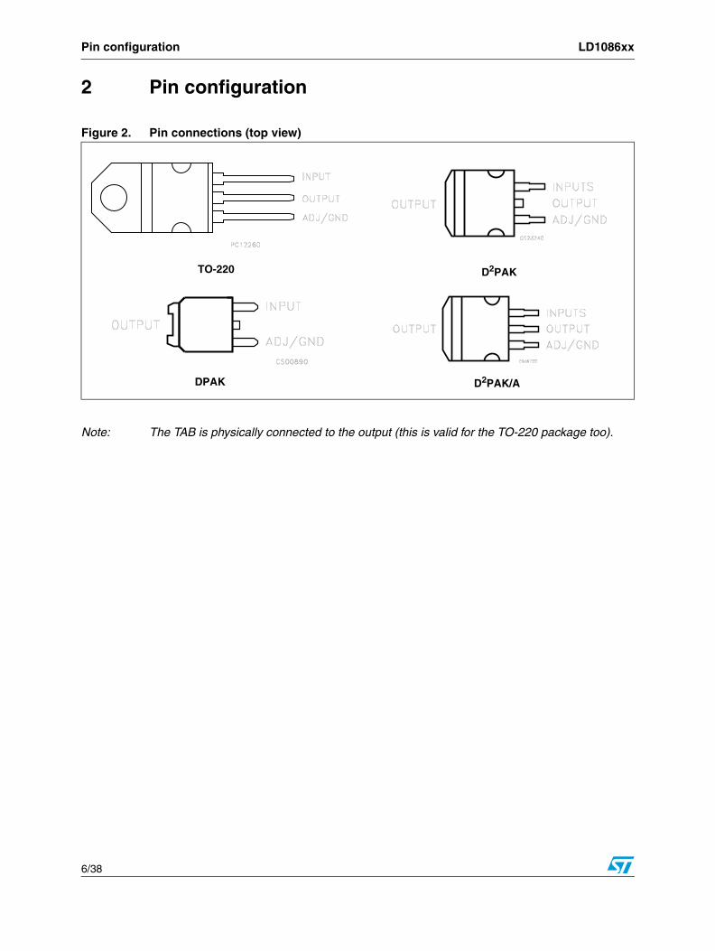
2 Pin configuration
Note: The TAB is physically connected to the output (this is valid for the TO-220 package too).
Figure 2. Pin connections (top view)
D2PAK
D2PAK/A
TO-220
DPAK
LD1086xx Maximum ratings
7/38
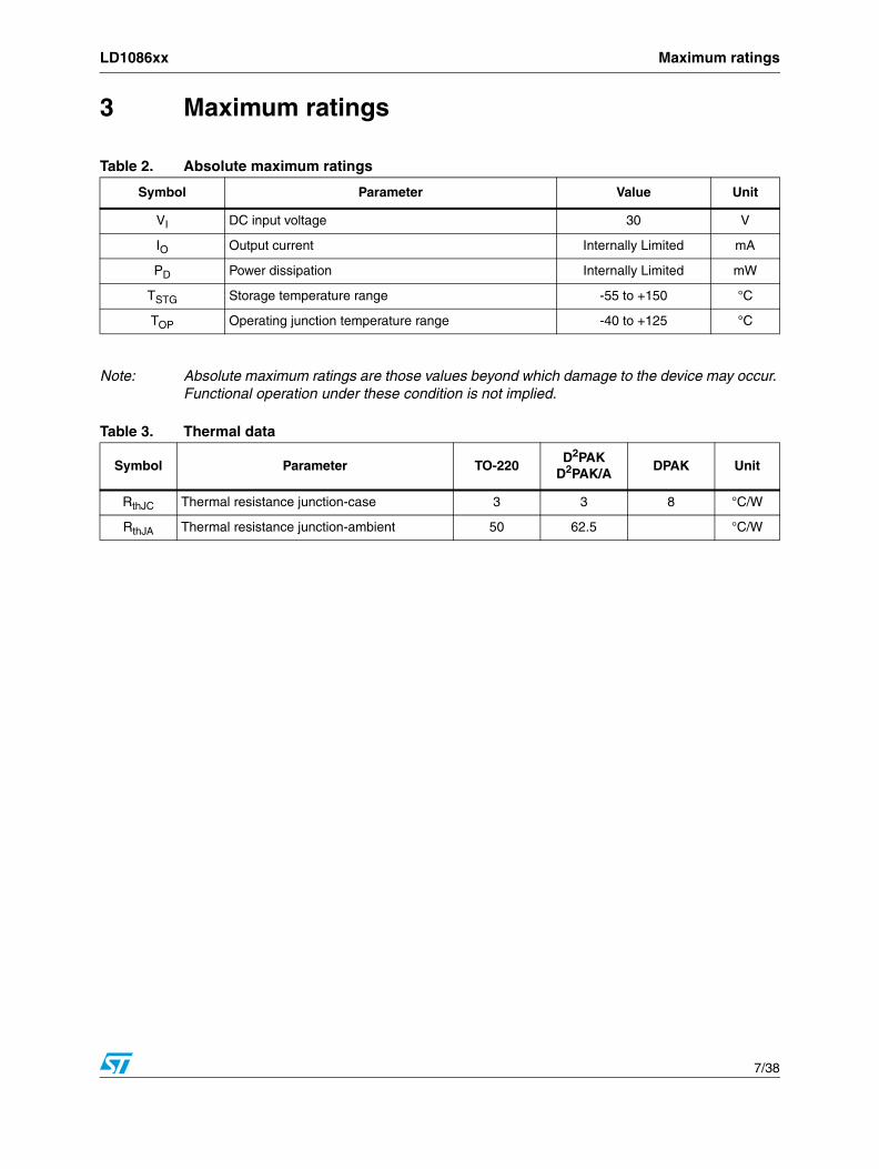
3 Maximum ratings
Note: Absolute maximum ratings are those values beyond which damage to the device may occur. Functional operation under these condition is not implied.
Table 2. Absolute maximum ratings
Symbol Parameter Value Unit
VI DC input voltage 30 V
IO Output current Internally Limited mA
PD Power dissipation Internally Limited mW
TSTG Storage temperature range -55 to +150 °C
TOP Operating junction temperature range -40 to +125 °C
Table 3. Thermal data
Symbol Parameter TO-220D2PAK
D2PAK/ADPAK Unit
RthJC Thermal resistance junction-case 3 3 8 °C/W
RthJA Thermal resistance junction-ambient 50 62.5 °C/W
Schematic application LD1086xx
8/38
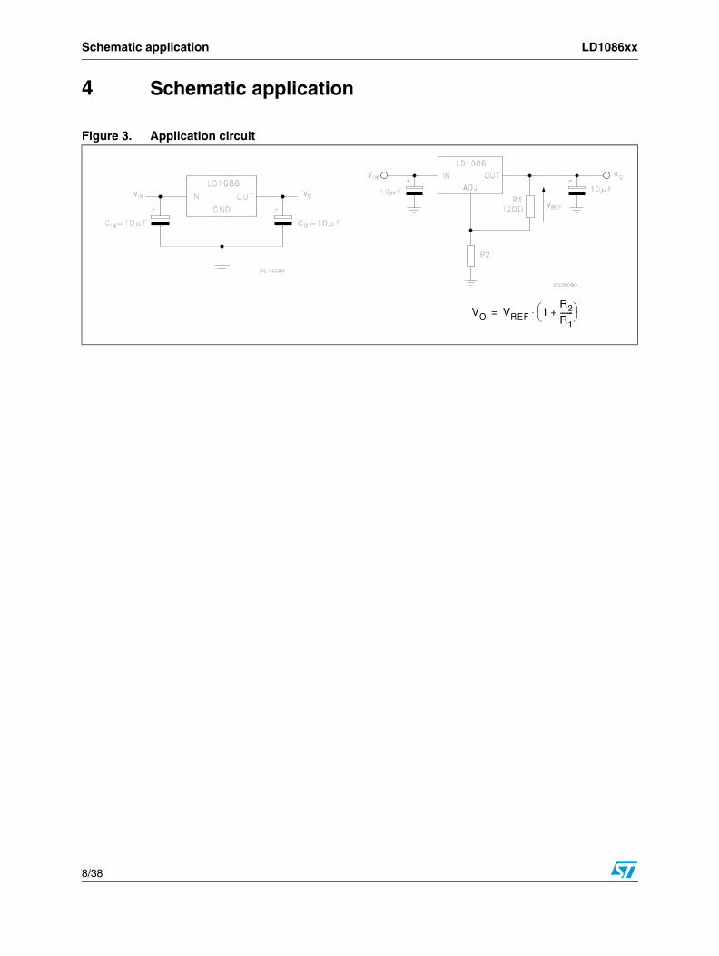
4 Schematic application
Figure 3. Application circuit
VO VREF 1R2
R1-------+⎝ ⎠
⎛ ⎞⋅=
LD1086xx Electrical characteristics
9/38
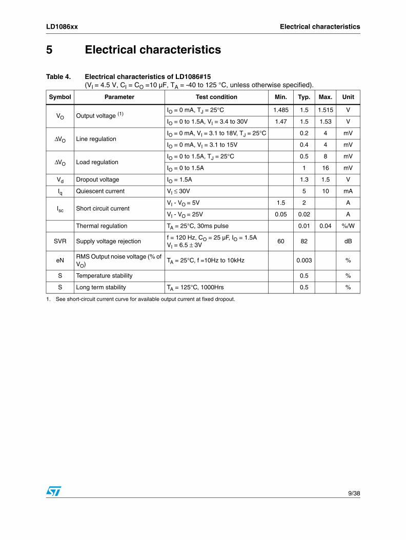
5 Electrical characteristics
Table 4. Electrical characteristics of LD1086#15(VI = 4.5 V, CI = CO =10 µF, TA = -40 to 125 °C, unless otherwise specified).
Symbol Parameter Test condition Min. Typ. Max. Unit
VO Output voltage (1)
1. See short-circuit current curve for available output current at fixed dropout.
IO = 0 mA, TJ = 25°C 1.485 1.5 1.515 V
IO = 0 to 1.5A, VI = 3.4 to 30V 1.47 1.5 1.53 V
ΔVO Line regulationIO = 0 mA, VI = 3.1 to 18V, TJ = 25°C 0.2 4 mV
IO = 0 mA, VI = 3.1 to 15V 0.4 4 mV
ΔVO Load regulationIO = 0 to 1.5A, TJ = 25°C 0.5 8 mV
IO = 0 to 1.5A 1 16 mV
Vd Dropout voltage IO = 1.5A 1.3 1.5 V
Iq Quiescent current VI ≤ 30V 5 10 mA
Isc Short circuit currentVI - VO = 5V 1.5 2 A
VI - VO = 25V 0.05 0.02 A
Thermal regulation TA = 25°C, 30ms pulse 0.01 0.04 %/W
SVR Supply voltage rejectionf = 120 Hz, CO = 25 µF, IO = 1.5AVI = 6.5 ± 3V
60 82 dB
eNRMS Output noise voltage (% of VO)
TA = 25°C, f =10Hz to 10kHz 0.003 %
S Temperature stability 0.5 %
S Long term stability TA = 125°C, 1000Hrs 0.5 %
Electrical characteristics LD1086xx
10/38
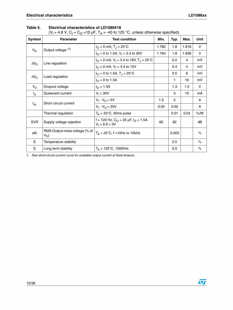
Table 5. Electrical characteristics of LD1086#18(VI = 4.8 V, CI = CO =10 µF, TA = -40 to 125 °C, unless otherwise specified).
Symbol Parameter Test condition Min. Typ. Max. Unit
VO Output voltage (1)IO = 0 mA, TJ = 25°C 1.782 1.8 1.818 V
IO = 0 to 1.5A, VI = 3.4 to 30V 1.764 1.8 1.836 V
ΔVO Line regulationIO = 0 mA, VI = 3.4 to 18V, TJ = 25°C 0.2 4 mV
IO = 0 mA, VI = 3.4 to 15V 0.4 4 mV
ΔVO Load regulationIO = 0 to 1.5A, TJ = 25°C 0.5 8 mV
IO = 0 to 1.5A 1 16 mV
Vd Dropout voltage IO = 1.5A 1.3 1.5 V
Iq Quiescent current VI ≤ 30V 5 10 mA
Isc Short circuit currentVI - VO = 5V 1.5 2 A
VI - VO = 25V 0.05 0.02 A
Thermal regulation TA = 25°C, 30ms pulse 0.01 0.04 %/W
SVR Supply voltage rejectionf = 120 Hz, CO = 25 µF, IO = 1.5A VI = 6.8 ± 3V
60 82 dB
eNRMS Output noise voltage (% of VO)
TA = 25°C, f =10Hz to 10kHz 0.003 %
S Temperature stability 0.5 %
S Long term stability TA = 125°C, 1000Hrs 0.5 %
1. See short-circuit current curve for available output current at fixed dropout.
LD1086xx Electrical characteristics
11/38
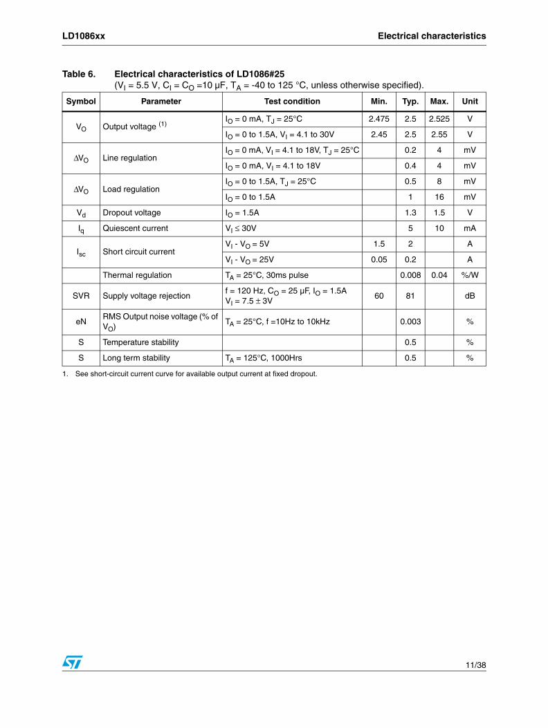
Table 6. Electrical characteristics of LD1086#25
(VI = 5.5 V, CI = CO =10 µF, TA = -40 to 125 °C, unless otherwise specified).
Symbol Parameter Test condition Min. Typ. Max. Unit
VO Output voltage (1)IO = 0 mA, TJ = 25°C 2.475 2.5 2.525 V
IO = 0 to 1.5A, VI = 4.1 to 30V 2.45 2.5 2.55 V
ΔVO Line regulationIO = 0 mA, VI = 4.1 to 18V, TJ = 25°C 0.2 4 mV
IO = 0 mA, VI = 4.1 to 18V 0.4 4 mV
ΔVO Load regulationIO = 0 to 1.5A, TJ = 25°C 0.5 8 mV
IO = 0 to 1.5A 1 16 mV
Vd Dropout voltage IO = 1.5A 1.3 1.5 V
Iq Quiescent current VI ≤ 30V 5 10 mA
Isc Short circuit currentVI - VO = 5V 1.5 2 A
VI - VO = 25V 0.05 0.2 A
Thermal regulation TA = 25°C, 30ms pulse 0.008 0.04 %/W
SVR Supply voltage rejectionf = 120 Hz, CO = 25 µF, IO = 1.5AVI = 7.5 ± 3V
60 81 dB
eNRMS Output noise voltage (% of VO)
TA = 25°C, f =10Hz to 10kHz 0.003 %
S Temperature stability 0.5 %
S Long term stability TA = 125°C, 1000Hrs 0.5 %
1. See short-circuit current curve for available output current at fixed dropout.
Electrical characteristics LD1086xx
12/38
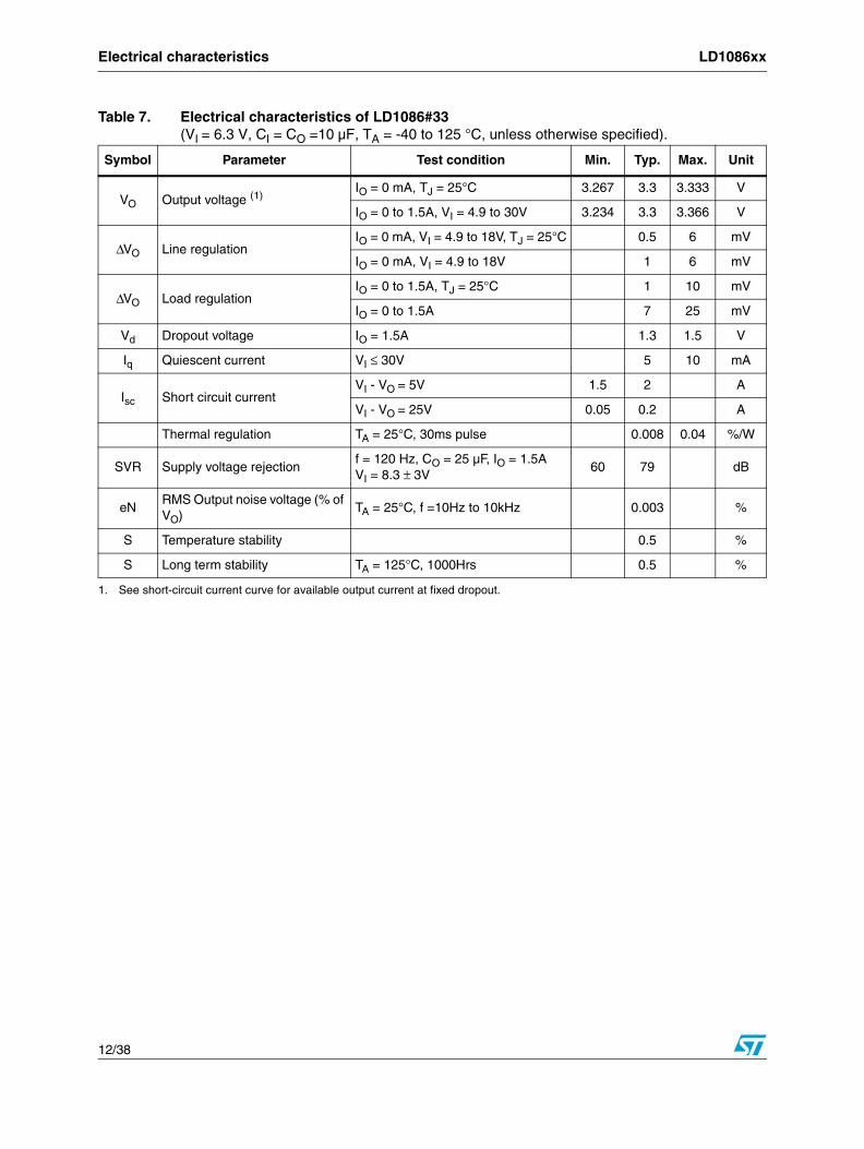
Table 7. Electrical characteristics of LD1086#33
(VI = 6.3 V, CI = CO =10 µF, TA = -40 to 125 °C, unless otherwise specified).
Symbol Parameter Test condition Min. Typ. Max. Unit
VO Output voltage (1)IO = 0 mA, TJ = 25°C 3.267 3.3 3.333 V
IO = 0 to 1.5A, VI = 4.9 to 30V 3.234 3.3 3.366 V
ΔVO Line regulationIO = 0 mA, VI = 4.9 to 18V, TJ = 25°C 0.5 6 mV
IO = 0 mA, VI = 4.9 to 18V 1 6 mV
ΔVO Load regulationIO = 0 to 1.5A, TJ = 25°C 1 10 mV
IO = 0 to 1.5A 7 25 mV
Vd Dropout voltage IO = 1.5A 1.3 1.5 V
Iq Quiescent current VI ≤ 30V 5 10 mA
Isc Short circuit currentVI - VO = 5V 1.5 2 A
VI - VO = 25V 0.05 0.2 A
Thermal regulation TA = 25°C, 30ms pulse 0.008 0.04 %/W
SVR Supply voltage rejectionf = 120 Hz, CO = 25 µF, IO = 1.5AVI = 8.3 ± 3V
60 79 dB
eNRMS Output noise voltage (% of VO)
TA = 25°C, f =10Hz to 10kHz 0.003 %
S Temperature stability 0.5 %
S Long term stability TA = 125°C, 1000Hrs 0.5 %
1. See short-circuit current curve for available output current at fixed dropout.

LD1086xx Electrical characteristics
13/38
Table 8. Electrical characteristics of LD1086#36
(VI = 6.6 V, CI = CO =10 µF, TA = -40 to 125 °C, unless otherwise specified).
Symbol Parameter Test condition Min. Typ. Max. Unit
VO Output voltage (1)IO = 0 mA, TJ = 25°C 3.564 3.6 3.636 V
IO = 0 to 1.5A, VI = 5.2 to 30V 3.528 3.6 3.672 V
ΔVO Line regulationIO = 0 mA, VI = 5.2 to 18V, TJ = 25°C 0.5 10 mV
IO = 0 mA, VI = 5.2 to 18V 1 10 mV
ΔVO Load regulationIO = 0 to 1.5A, TJ = 25°C 3 15 mV
IO = 0 to 1.5A 7 25 mV
Vd Dropout voltage IO = 1.5A 1.3 1.5 V
Iq Quiescent current VI ≤ 30V 5 10 mA
Isc Short circuit currentVI - VO = 5V 1.5 2 A
VI - VO = 25V 0.05 0.2 A
Thermal regulation TA = 25°C, 30ms pulse 0.01 0.04 %/W
SVR Supply voltage rejectionf = 120 Hz, CO = 25 µF, IO = 1.5AVI = 8.6 ± 3V
60 78 dB
eNRMS Output noise voltage (% of VO)
TA = 25°C, f =10Hz to 10kHz 0.003 %
S Temperature stability 0.5 %
S Long term stability TA = 125°C, 1000Hrs 0.5 %
1. See short-circuit current curve for available output current at fixed dropout.
Electrical characteristics LD1086xx
14/38
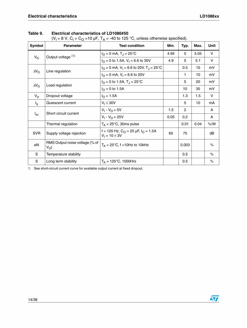
Table 9. Electrical characteristics of LD1086#50
(VI = 8 V, CI = CO =10 µF, TA = -40 to 125 °C, unless otherwise specified).
Symbol Parameter Test condition Min. Typ. Max. Unit
VO Output voltage (1)IO = 0 mA, TJ = 25°C 4.95 5 5.05 V
IO = 0 to 1.5A, VI = 6.6 to 30V 4.9 5 5.1 V
ΔVO Line regulationIO = 0 mA, VI = 6.6 to 20V, TJ = 25°C 0.5 10 mV
IO = 0 mA, VI = 6.6 to 20V 1 10 mV
ΔVO Load regulationIO = 0 to 1.5A, TJ = 25°C 5 20 mV
IO = 0 to 1.5A 10 35 mV
Vd Dropout voltage IO = 1.5A 1.3 1.5 V
Iq Quiescent current VI ≤ 30V 5 10 mA
Isc Short circuit currentVI - VO = 5V 1.5 2 A
VI - VO = 25V 0.05 0.2 A
Thermal regulation TA = 25°C, 30ms pulse 0.01 0.04 %/W
SVR Supply voltage rejectionf = 120 Hz, CO = 25 µF, IO = 1.5A VI = 10 ± 3V
60 75 dB
eNRMS Output noise voltage (% of VO)
TA = 25°C, f =10Hz to 10kHz 0.003 %
S Temperature stability 0.5 %
S Long term stability TA = 125°C, 1000Hrs 0.5 %
1. See short-circuit current curve for available output current at fixed dropout.
LD1086xx Electrical characteristics
15/38
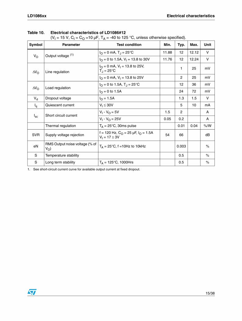
Table 10. Electrical characteristics of LD1086#12
(VI = 15 V, CI = CO =10 µF, TA = -40 to 125 °C, unless otherwise specified).
Symbol Parameter Test condition Min. Typ. Max. Unit
VO Output voltage (1)IO = 0 mA, TJ = 25°C 11.88 12 12.12 V
IO = 0 to 1.5A, VI = 13.8 to 30V 11.76 12 12.24 V
ΔVO Line regulation
IO = 0 mA, VI = 13.8 to 25V,TJ = 25°C
1 25 mV
IO = 0 mA, VI = 13.8 to 25V 2 25 mV
ΔVO Load regulationIO = 0 to 1.5A, TJ = 25°C 12 36 mV
IO = 0 to 1.5A 24 72 mV
Vd Dropout voltage IO = 1.5A 1.3 1.5 V
Iq Quiescent current VI ≤ 30V 5 10 mA
Isc Short circuit currentVI - VO = 5V 1.5 2 A
VI - VO = 25V 0.05 0.2 A
Thermal regulation TA = 25°C, 30ms pulse 0.01 0.04 %/W
SVR Supply voltage rejectionf = 120 Hz, CO = 25 µF, IO = 1.5A VI = 17 ± 3V
54 66 dB
eNRMS Output noise voltage (% of VO)
TA = 25°C, f =10Hz to 10kHz 0.003 %
S Temperature stability 0.5 %
S Long term stability TA = 125°C, 1000Hrs 0.5 %
1. See short-circuit current curve for available output current at fixed dropout.
Electrical characteristics LD1086xx
16/38
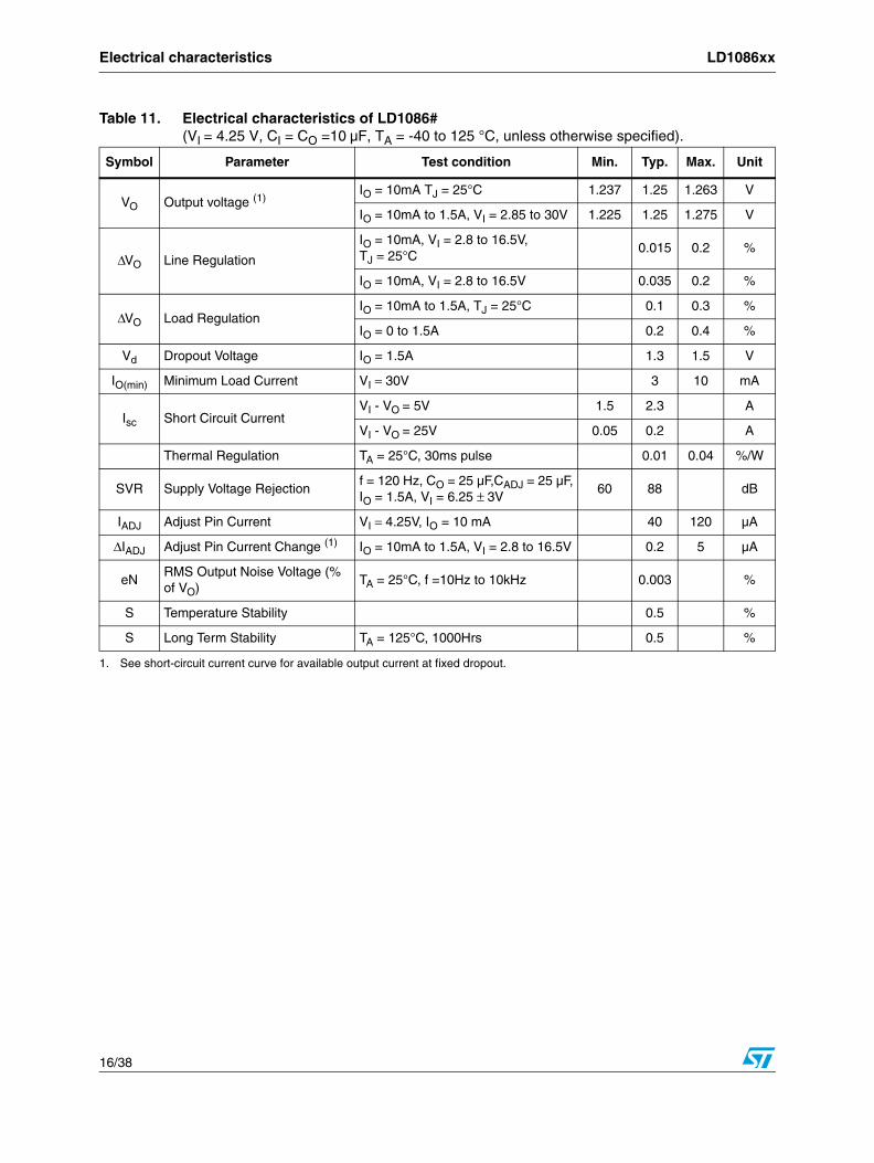
Table 11. Electrical characteristics of LD1086#
(VI = 4.25 V, CI = CO =10 µF, TA = -40 to 125 °C, unless otherwise specified).
Symbol Parameter Test condition Min. Typ. Max. Unit
VO Output voltage (1)IO = 10mA TJ = 25°C 1.237 1.25 1.263 V
IO = 10mA to 1.5A, VI = 2.85 to 30V 1.225 1.25 1.275 V
ΔVO Line Regulation
IO = 10mA, VI = 2.8 to 16.5V,TJ = 25°C
0.015 0.2 %
IO = 10mA, VI = 2.8 to 16.5V 0.035 0.2 %
ΔVO Load RegulationIO = 10mA to 1.5A, TJ = 25°C 0.1 0.3 %
IO = 0 to 1.5A 0.2 0.4 %
Vd Dropout Voltage IO = 1.5A 1.3 1.5 V
IO(min) Minimum Load Current VI = 30V 3 10 mA
Isc Short Circuit CurrentVI - VO = 5V 1.5 2.3 A
VI - VO = 25V 0.05 0.2 A
Thermal Regulation TA = 25°C, 30ms pulse 0.01 0.04 %/W
SVR Supply Voltage Rejectionf = 120 Hz, CO = 25 µF,CADJ = 25 µF,IO = 1.5A, VI = 6.25 ± 3V
60 88 dB
IADJ Adjust Pin Current VI = 4.25V, IO = 10 mA 40 120 µA
ΔIADJ Adjust Pin Current Change (1) IO = 10mA to 1.5A, VI = 2.8 to 16.5V 0.2 5 µA
eNRMS Output Noise Voltage (% of VO)
TA = 25°C, f =10Hz to 10kHz 0.003 %
S Temperature Stability 0.5 %
S Long Term Stability TA = 125°C, 1000Hrs 0.5 %
1. See short-circuit current curve for available output current at fixed dropout.
LD1086xx Electrical characteristics
17/38
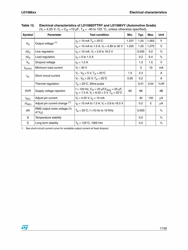
Table 12. Electrical characteristics of LD1086DTTRY and LD1086VY (Automotive Grade)
(VI = 4.25 V, CI = CO =10 µF, TA = -40 to 125 °C, unless otherwise specified).
Symbol Parameter Test condition Min. Typ. Max. Unit
VO Output voltage (1)IO = 10 mA TA = 25°C 1.237 1.25 1.263 V
IO = 10 mA to 1.5 A, VI = 2.85 to 30 V 1.225 1.25 1.275 V
ΔVO Line regulation IO = 10 mA, VI = 2.8 to 16.5 V 0.035 0.2 %
ΔVO Load regulation IO = 0 to 1.5 A 0.2 0.4 %
Vd Dropout voltage IO = 1.5 A 1.3 1.5 V
IO(min) Minimum load current VI = 30 V 3 10 mA
Isc Short circuit currentVI - VO = 5 V, TA = 25°C 1.5 2.3 A
VI - VO = 25 V, TA = 25°C 0.05 0.2 A
Thermal regulation TA = 25°C, 30ms pulse 0.01 0.04 %/W
SVR Supply voltage rejectionf = 120 Hz, CO = 25 µF,CADJ = 25 µF,IO = 1.5 A, VI = 6.25 ± 3 V, TA = 25°C
60 88 dB
IADJ Adjust pin current VI = 4.25 V, IO = 10 mA 40 120 μA
ΔIADJ Adjust pin current change (1) IO = 10 mA to 1.5 A, VI = 2.8 to 16.5 V 0.2 5 μA
eNRMS output noise voltage (% of VO)
TA = 25°C, f =10 Hz to 10 KHz 0.003 %
S Temperature stability 0.5 %
S Long term stability TA = 125°C, 1000 Hrs 0.5 %
1. See short-circuit current curve for available output current at fixed dropout.
Typical application LD1086xx
18/38
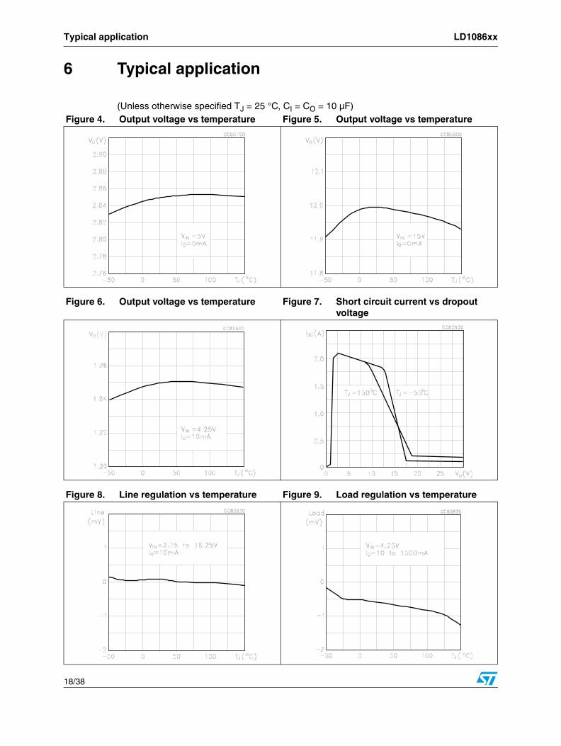
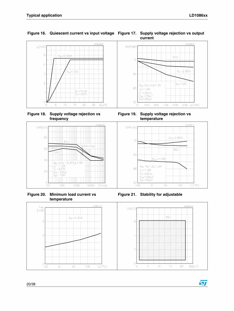
6 Typical application
(Unless otherwise specified TJ = 25 °C, CI = CO = 10 µF)Figure 4. Output voltage vs temperature Figure 5. Output voltage vs temperature
Figure 6. Output voltage vs temperature Figure 7. Short circuit current vs dropout voltage
Figure 8. Line regulation vs temperature Figure 9. Load regulation vs temperature
LD1086xx Typical application
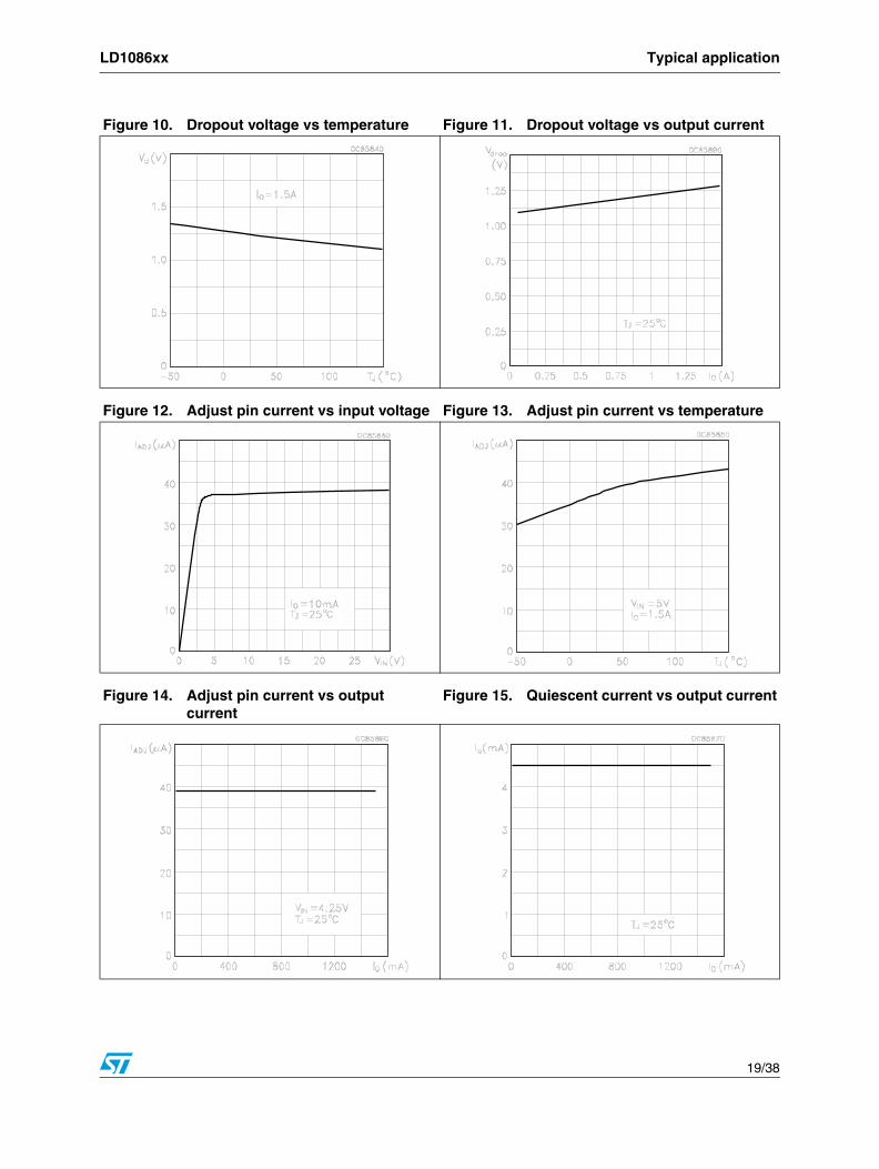
19/38
Figure 10. Dropout voltage vs temperature Figure 11. Dropout voltage vs output current
Figure 12. Adjust pin current vs input voltage Figure 13. Adjust pin current vs temperature
Figure 14. Adjust pin current vs output current
Figure 15. Quiescent current vs output current
Typical application LD1086xx
20/38
Figure 16. Quiescent current vs input voltage Figure 17. Supply voltage rejection vs output current
Figure 18. Supply voltage rejection vs frequency
Figure 19. Supply voltage rejection vs temperature
Figure 20. Minimum load current vs temperature
Figure 21. Stability for adjustable
LD1086xx Typical application
21/38
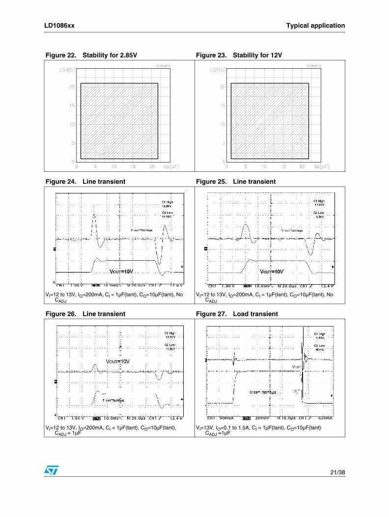
Figure 22. Stability for 2.85V Figure 23. Stability for 12V
Figure 24. Line transient Figure 25. Line transient
VI=12 to 13V, IO=200mA, CI = 1µF(tant), CO=10µF(tant), No CADJ
VI=12 to 13V, IO=200mA, CI = 1µF(tant), CO=10µF(tant), No CADJ
Figure 26. Line transient Figure 27. Load transient
VI=12 to 13V, IO=200mA, CI = 1µF(tant), CO=10µF(tant), CADJ = 1µF
VI=13V, IO=0.1 to 1.5A, CI = 1µF(tant), CO=10µF(tant)CADJ =1µF
Typical application LD1086xx
22/38
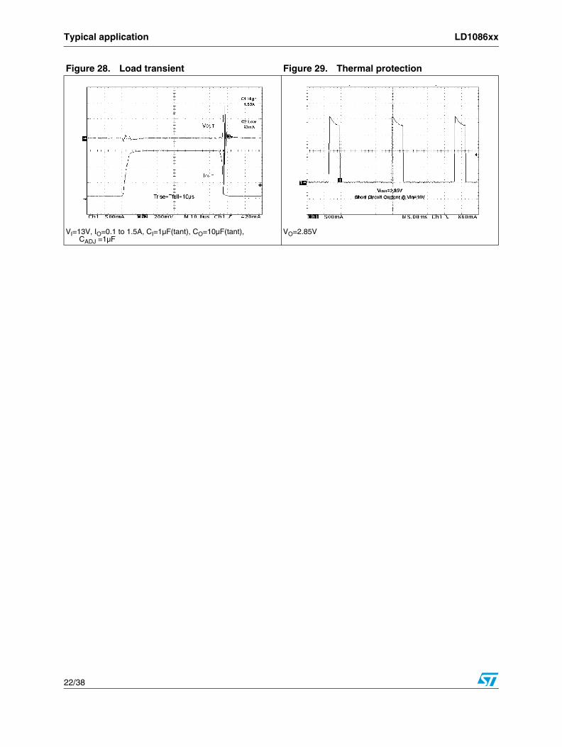
Figure 28. Load transient Figure 29. Thermal protection
VI=13V, IO=0.1 to 1.5A, CI=1µF(tant), CO=10µF(tant),CADJ =1µF
VO=2.85V
LD1086xx Package mechanical data
23/38
7 Package mechanical data
In order to meet environmental requirements, ST offers these devices in ECOPACK® packages. These packages have a lead-free second level interconnect. The category of second Level Interconnect is marked on the package and on the inner box label, in compliance with JEDEC Standard JESD97. The maximum ratings related to soldering conditions are also marked on the inner box label. ECOPACK is an ST trademark. ECOPACK specifications are available at: www.st.com.
Package mechanical data LD1086xx
24/38
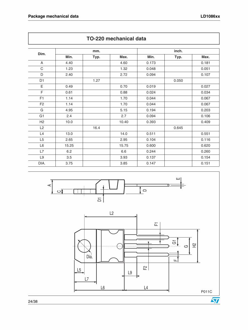
Dim.mm. inch.
Min. Typ. Max. Min. Typ. Max.
A 4.40 4.60 0.173 0.181
C 1.23 1.32 0.048 0.051
D 2.40 2.72 0.094 0.107
D1 1.27 0.050
E 0.49 0.70 0.019 0.027
F 0.61 0.88 0.024 0.034
F1 1.14 1.70 0.044 0.067
F2 1.14 1.70 0.044 0.067
G 4.95 5.15 0.194 0.203
G1 2.4 2.7 0.094 0.106
H2 10.0 10.40 0.393 0.409
L2 16.4 0.645
L4 13.0 14.0 0.511 0.551
L5 2.65 2.95 0.104 0.116
L6 15.25 15.75 0.600 0.620
L7 6.2 6.6 0.244 0.260
L9 3.5 3.93 0.137 0.154
DIA. 3.75 3.85 0.147 0.151
TO-220 mechanical data
P011C
LD1086xx Package mechanical data
25/38
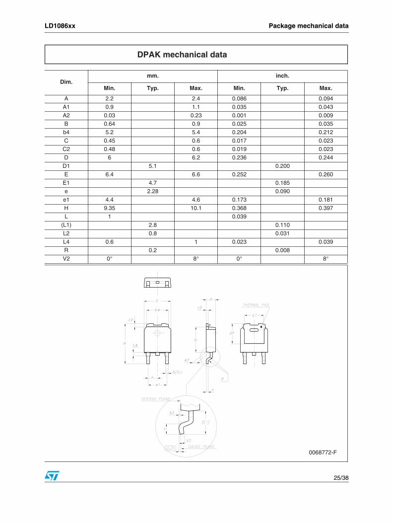
Dim.mm. inch.
Min. Typ. Max. Min. Typ. Max.
A 2.2 2.4 0.086 0.094
A1 0.9 1.1 0.035 0.043
A2 0.03 0.23 0.001 0.009
B 0.64 0.9 0.025 0.035
b4 5.2 5.4 0.204 0.212
C 0.45 0.6 0.017 0.023
C2 0.48 0.6 0.019 0.023
D 6 6.2 0.236 0.244
D1 5.1 0.200
E 6.4 6.6 0.252 0.260
E1 4.7 0.185
e 2.28 0.090
e1 4.4 4.6 0.173 0.181
H 9.35 10.1 0.368 0.397
L 1 0.039
(L1) 2.8 0.110
L2 0.8 0.031
L4 0.6 1 0.023 0.039
R 0.2 0.008
V2 0° 8° 0° 8°
DPAK mechanical data
0068772-F
Package mechanical data LD1086xx
26/38
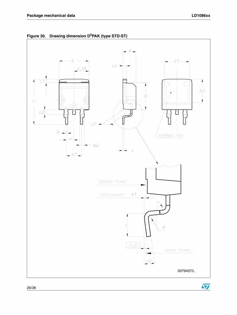
Figure 30. Drawing dimension D2PAK (type STD-ST)
0079457/L
LD1086xx Package mechanical data
27/38
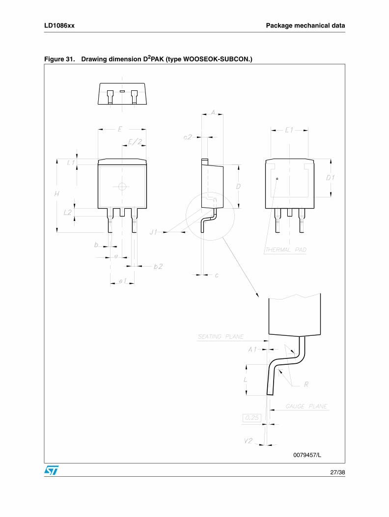
Figure 31. Drawing dimension D2PAK (type WOOSEOK-SUBCON.)
0079457/L

Package mechanical data LD1086xx
28/38
Note: The D2PAK package coming from the subcontractor Wooseok is fully compatible with the ST's package suggested footprint.
Table 13. D2PAK mechanical data
Dim.
Type STD-ST Type WOOSEOK-SUBCON.
mm. mm.
Min. Typ. Max. Min. Typ. Max.
A 4.40 4.60 4.30 4.70
A1 0.03 0.23 0 0.20
b 0.70 0.93 0.70 0.90
b2 1.14 1.70 1.17 1.37
c 0.45 0.60 0.45 0.50 0.60
c2 1.23 1.36 1.25 1.30 1.40
D 8.95 9.35 9 9.20 9.40
D1 7.50 7.50
E 10 10.40 9.80 10.20
E1 8.50 7.50
e 2.54 2.54
e1 4.88 5.28 5.08
H 15 15.85 15 15.30 15.60
J1 2.49 2.69 2.20 2.60
L 2.29 2.79 1.79 2.79
L1 1.27 1.40 1 1.40
L2 1.30 1.75 1.20 1.60
R 0.4 0.30
V2 0° 8° 0° 3°
LD1086xx Package mechanical data
29/38
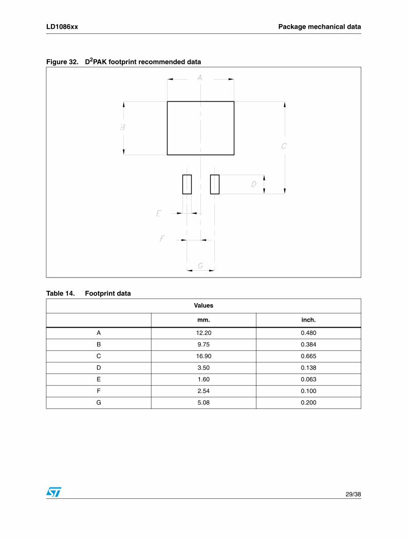
Figure 32. D2PAK footprint recommended data
Table 14. Footprint data
Values
mm. inch.
A 12.20 0.480
B 9.75 0.384
C 16.90 0.665
D 3.50 0.138
E 1.60 0.063
F 2.54 0.100
G 5.08 0.200
Package mechanical data LD1086xx
30/38
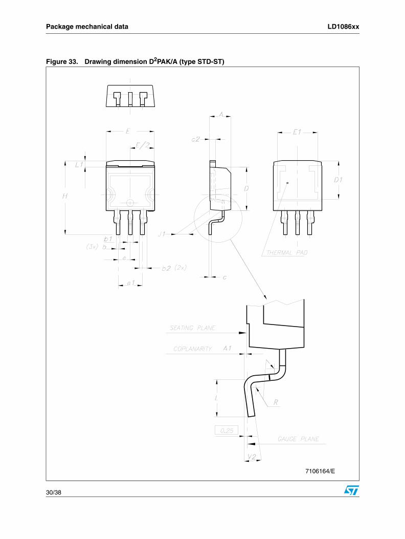
Figure 33. Drawing dimension D2PAK/A (type STD-ST)
7106164/E
LD1086xx Package mechanical data
31/38
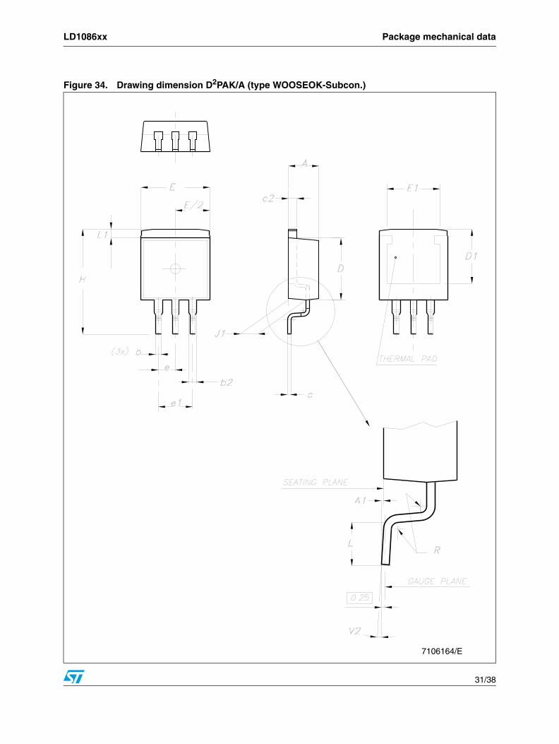
Figure 34. Drawing dimension D2PAK/A (type WOOSEOK-Subcon.)
7106164/E
Package mechanical data LD1086xx
32/38
Note: The D2PAK/A package coming from the subcontractor Wooseok is fully compatible with the ST's package suggested footprint.
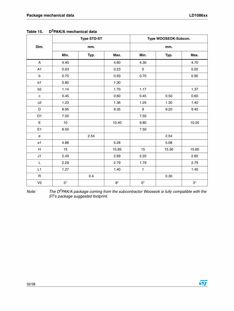
Table 15. D2PAK/A mechanical data
Dim.
Type STD-ST Type WOOSEOK-Subcon.
mm. mm.
Min. Typ. Max. Min. Typ. Max.
A 4.40 4.60 4.30 4.70
A1 0.03 0.23 0 0.20
b 0.70 0.93 0.70 0.90
b1 0.80 1.30
b2 1.14 1.70 1.17 1.37
c 0.45 0.60 0.45 0.50 0.60
c2 1.23 1.36 1.25 1.30 1.40
D 8.95 9.35 9 9.20 9.40
D1 7.50 7.50
E 10 10.40 9.80 10.20
E1 8.50 7.50
e 2.54 2.54
e1 4.88 5.28 5.08
H 15 15.85 15 15.30 15.60
J1 2.49 2.69 2.20 2.60
L 2.29 2.79 1.79 2.79
L1 1.27 1.40 1 1.40
R 0.4 0.30
V2 0° 8° 0° 3°
LD1086xx Package mechanical data
33/38
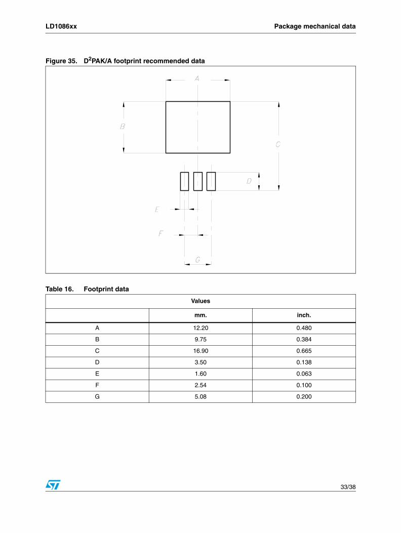
Figure 35. D2PAK/A footprint recommended data
Table 16. Footprint data
Values
mm. inch.
A 12.20 0.480
B 9.75 0.384
C 16.90 0.665
D 3.50 0.138
E 1.60 0.063
F 2.54 0.100
G 5.08 0.200
Package mechanical data LD1086xx
34/38
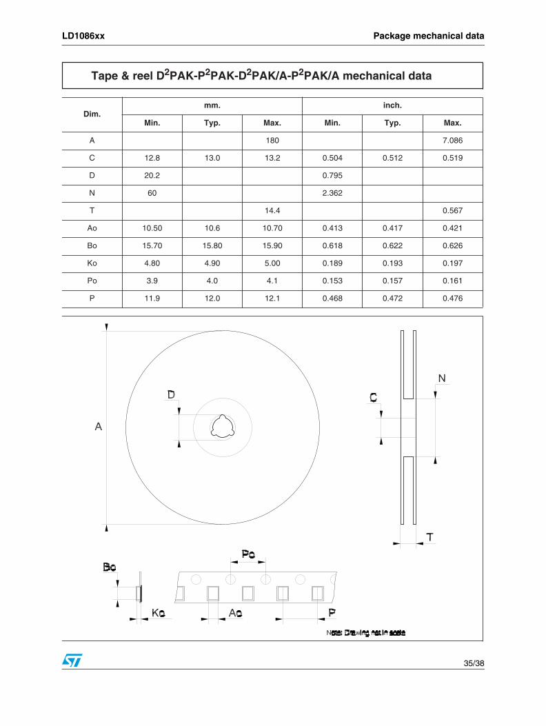
Dim.mm. inch.
Min. Typ. Max. Min. Typ. Max.
A 330 12.992
C 12.8 13.0 13.2 0.504 0.512 0.519
D 20.2 0.795
N 60 2.362
T 22.4 0.882
Ao 6.80 6.90 7.00 0.268 0.272 0.2.76
Bo 10.40 10.50 10.60 0.409 0.413 0.417
Ko 2.55 2.65 2.75 0.100 0.104 0.105
Po 3.9 4.0 4.1 0.153 0.157 0.161
P 7.9 8.0 8.1 0.311 0.315 0.319
Tape & reel DPAK-PPAK mechanical data
LD1086xx Package mechanical data
35/38
Dim.mm. inch.
Min. Typ. Max. Min. Typ. Max.
A 180 7.086
C 12.8 13.0 13.2 0.504 0.512 0.519
D 20.2 0.795
N 60 2.362
T 14.4 0.567
Ao 10.50 10.6 10.70 0.413 0.417 0.421
Bo 15.70 15.80 15.90 0.618 0.622 0.626
Ko 4.80 4.90 5.00 0.189 0.193 0.197
Po 3.9 4.0 4.1 0.153 0.157 0.161
P 11.9 12.0 12.1 0.468 0.472 0.476
Tape & reel D2PAK-P2PAK-D2PAK/A-P2PAK/A mechanical data
Order codes LD1086xx
36/38
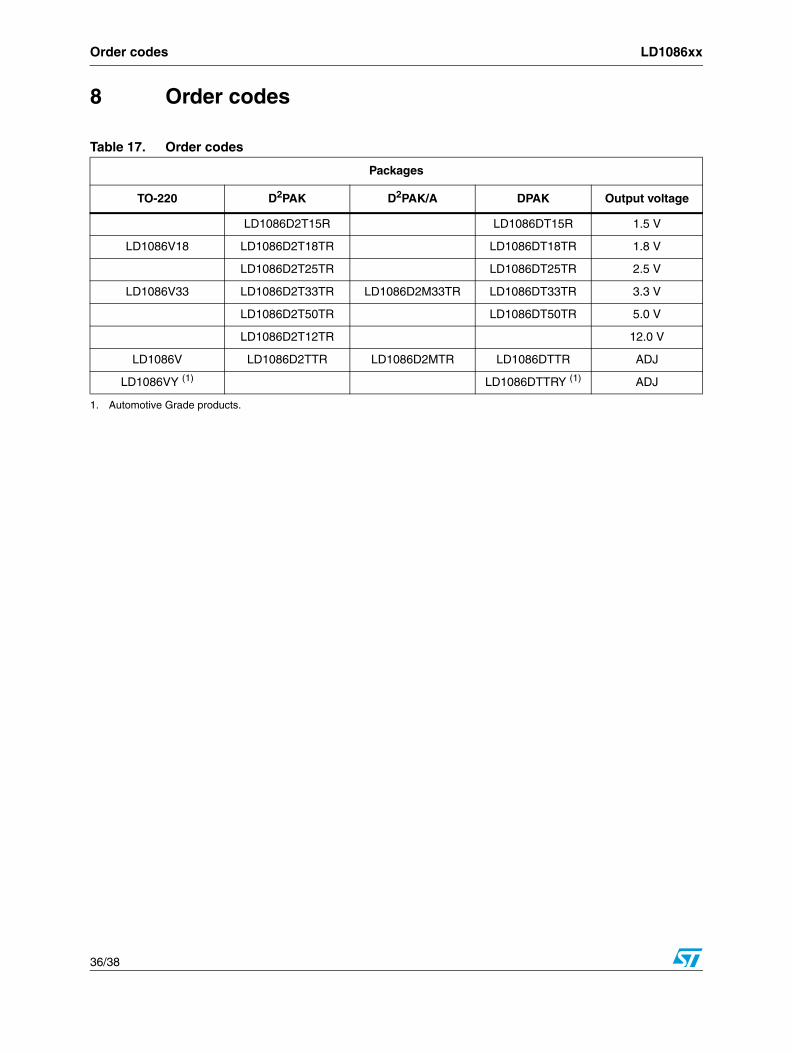
8 Order codes
Table 17. Order codes
Packages
TO-220 D2PAK D2PAK/A DPAK Output voltage
LD1086D2T15R LD1086DT15R 1.5 V
LD1086V18 LD1086D2T18TR LD1086DT18TR 1.8 V
LD1086D2T25TR LD1086DT25TR 2.5 V
LD1086V33 LD1086D2T33TR LD1086D2M33TR LD1086DT33TR 3.3 V
LD1086D2T50TR LD1086DT50TR 5.0 V
LD1086D2T12TR 12.0 V
LD1086V LD1086D2TTR LD1086D2MTR LD1086DTTR ADJ
LD1086VY (1) LD1086DTTRY (1)
1. Automotive Grade products.
ADJ
LD1086xx Revision history
37/38
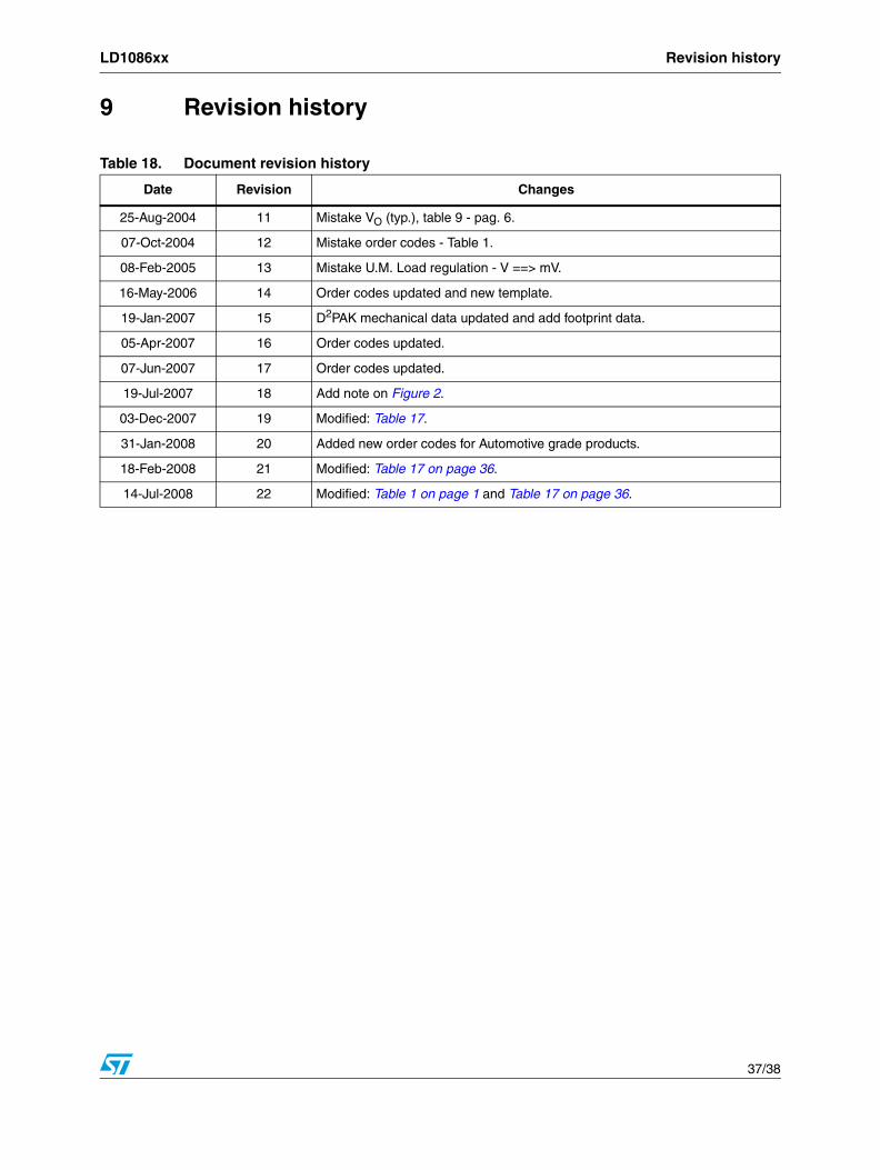
9 Revision history
Table 18. Document revision history
Date Revision Changes
25-Aug-2004 11 Mistake VO (typ.), table 9 - pag. 6.
07-Oct-2004 12 Mistake order codes - Table 1.
08-Feb-2005 13 Mistake U.M. Load regulation - V ==> mV.
16-May-2006 14 Order codes updated and new template.
19-Jan-2007 15 D2PAK mechanical data updated and add footprint data.
05-Apr-2007 16 Order codes updated.
07-Jun-2007 17 Order codes updated.
19-Jul-2007 18 Add note on Figure 2.
03-Dec-2007 19 Modified: Table 17.
31-Jan-2008 20 Added new order codes for Automotive grade products.
18-Feb-2008 21 Modified: Table 17 on page 36.
14-Jul-2008 22 Modified: Table 1 on page 1 and Table 17 on page 36.
LD1086xx
38/38
Please Read Carefully:
Information in this document is provided solely in connection with ST products. STMicroelectronics NV and its subsidiaries (“ST”) reserve theright to make changes, corrections, modifications or improvements, to this document, and the products and services described herein at anytime, without notice.
All ST products are sold pursuant to ST’s terms and conditions of sale.
Purchasers are solely responsible for the choice, selection and use of the ST products and services described herein, and ST assumes noliability whatsoever relating to the choice, selection or use of the ST products and services described herein.
No license, express or implied, by estoppel or otherwise, to any intellectual property rights is granted under this document. If any part of thisdocument refers to any third party products or services it shall not be deemed a license grant by ST for the use of such third party productsor services, or any intellectual property contained therein or considered as a warranty covering the use in any manner whatsoever of suchthird party products or services or any intellectual property contained therein.
UNLESS OTHERWISE SET FORTH IN ST’S TERMS AND CONDITIONS OF SALE ST DISCLAIMS ANY EXPRESS OR IMPLIEDWARRANTY WITH RESPECT TO THE USE AND/OR SALE OF ST PRODUCTS INCLUDING WITHOUT LIMITATION IMPLIEDWARRANTIES OF MERCHANTABILITY, FITNESS FOR A PARTICULAR PURPOSE (AND THEIR EQUIVALENTS UNDER THE LAWSOF ANY JURISDICTION), OR INFRINGEMENT OF ANY PATENT, COPYRIGHT OR OTHER INTELLECTUAL PROPERTY RIGHT.
UNLESS EXPRESSLY APPROVED IN WRITING BY AN AUTHORIZED ST REPRESENTATIVE, ST PRODUCTS ARE NOTRECOMMENDED, AUTHORIZED OR WARRANTED FOR USE IN MILITARY, AIR CRAFT, SPACE, LIFE SAVING, OR LIFE SUSTAININGAPPLICATIONS, NOR IN PRODUCTS OR SYSTEMS WHERE FAILURE OR MALFUNCTION MAY RESULT IN PERSONAL INJURY,DEATH, OR SEVERE PROPERTY OR ENVIRONMENTAL DAMAGE. ST PRODUCTS WHICH ARE NOT SPECIFIED AS "AUTOMOTIVEGRADE" MAY ONLY BE USED IN AUTOMOTIVE APPLICATIONS AT USER’S OWN RISK.
Resale of ST products with provisions different from the statements and/or technical features set forth in this document shall immediately voidany warranty granted by ST for the ST product or service described herein and shall not create or extend in any manner whatsoever, anyliability of ST.
ST and the ST logo are trademarks or registered trademarks of ST in various countries.
Information in this document supersedes and replaces all information previously supplied.
The ST logo is a registered trademark of STMicroelectronics. All other names are the property of their respective owners.
© 2008 STMicroelectronics - All rights reserved
STMicroelectronics group of companies
Australia - Belgium - Brazil - Canada - China - Czech Republic - Finland - France - Germany - Hong Kong - India - Israel - Italy - Japan - Malaysia - Malta - Morocco - Singapore - Spain - Sweden - Switzerland - United Kingdom - United States of America
www.st.com