Embed Size (px)
Citation preview
Mobile LPDDR4 SDRAMMT53B256M32D1, MT53B512M32D2, MT53B1024M32D4
Features• Ultra-low-voltage core and I/O power supplies
– VDD1 = 1.70–1.95V; 1.8V nominal– VDD2/VDDQ = 1.06–1.17V; 1.10V nominal
• Frequency range– 1600–10 MHz (data rate range: 3200–20 Mb/s/
pin)• 16n prefetch DDR architecture• 2-channel partitioned architecture for low RD/WR
energy and low average latency• 8 internal banks per channel for concurrent opera-
tion• Single-data-rate CMD/ADR entry• Bidirectional/differential data strobe per byte lane• Programmable READ and WRITE latencies (RL/WL)• Programmable and on-the-fly burst lengths (BL =
16, 32)• Directed per-bank refresh for concurrent bank op-
eration and ease of command scheduling• Up to 12.8 GB/s per die (2 channels x 6.4 GB/s)• On-chip temperature sensor to control self refresh
rate• Partial-array self refresh (PASR)• Selectable output drive strength (DS)• Clock-stop capability• RoHS-compliant, “green” packaging• Programmable VSSQ (ODT) termination
Options Marking• VDD1/VDD2: 1.8V/1.1V B• Array configuration
– 256 Meg x 32 (2 channels x16 I/O) 256M32– 512 Meg x 32 (2 channels x16 I/O) 512M32– 1024 Meg x 32 (2 channels x8 I/O x 2) 1024M32
• Device configuration – 256M16 x 2 channel x 1 die D1– 256M16 x 2 channel x 2 die D2– 512M8 x 2 channel x 4 die D4
• FBGA “green” package – 200-ball WFBGA (10mm x 14.5mm x
0.80mm)NP
– 200-ball VFBGA (10mm x 14.5mm x0.95mm)
NQ
• Speed grade, cycle time -062– 625ps @ RL = 28/32 (x16 device)– 625ps @ RL = 32/36 (x8 device)
• Operating temperature range – –30°C to +85°C WT
• Revision :C
Table 1: Key Timing Parameters
SpeedGrade
Arrayconfigura-
tionDeviceType
Clock Rate(MHz)
Data Rate(Mb/s/pin)
WRITE Latency READ Latency
Set A Set BDBI
DisabledDBI
Enabled
-062 256Mb x 32512Mb x 32
x16 device 1600 3200 14 26 28 32
1024Mb x 32 x8 device 1600 3200 14 26 32 36
Micron Confidential and Proprietary Preliminary‡
200b: x32 Mobile LPDDR4 SDRAMFeatures
PDF: 09005aef8653a92d200b_z01m_sdp_ddp_qdp_mobile_lpddr4.pdf – Rev. B 4/16 EN 1 Micron Technology, Inc. reserves the right to change products or specifications without notice.
© 2015 Micron Technology, Inc. All rights reserved.
‡Products and specifications discussed herein are for evaluation and reference purposes only and are subject to change byMicron without notice. Products are only warranted by Micron to meet Micron’s production data sheet specifications.
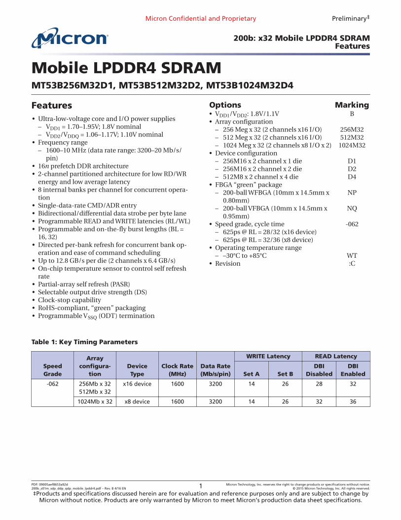
SDRAM AddressingThe table below shows the addressing for the 8Gb die density. Where applicable, a distinction is made betweenper-channel and per-die parameters. All bank, row, and column addresses are shown per-channel.
Table 2: Device Addressing
Configuration 256M32 (8Gb) 512M32 (16Gb) 1024M32 (32Gb) 3
Die per package 1 2 4
Device density (per die) 8Gb 8Gb 8Gb
Device density (per channel) 4Gb 8Gb 16Gb
Configuration 32Mb x 16 DQ x 8 banksx 2 channels x 1 rank
32Mb x 16 DQ x 8 banksx 2 channels x 2 ranks
64Mb x 8 DQ x 8 banksx 2 channels x 2 ranks x 2
Number of channels (per die) 2 2 2
Number of ranks per channel 1 2 2
Number of banks (per channel) 8 8 8
Array prefetch (bits) (per channel) 256 256 128
Number of rows (per bank) 32,768 32,768 65,536
Number of columns (fetch boundaries) 64 64 32
Page size (bytes) 2048 2048 1024
Channel density (bits per channel) 4,294,967,296 8,589,934,592 17,179,869,184
Total density (bits per die) 8,589,934,592 8,589,934,592 8,589,934,592
Bank address BA[2:0] BA[2:0] BA[2:0]
x16 Row addresses R[14:0] R[14:0] –
Column addresses C[9:0] C[9:0] –
x8 Row addresses – – R[15:0]
Column addresses – – C[9:0]
Burst starting address boundary 64-bit 64-bit 64-bit
Notes: 1. The lower two column addresses (C0–C1) are assumed to be zero and are not transmitted on the CA bus.2. Row and column address values on the CA bus that are not used for a particular density are "Don't Care."3. Refer to Byte Mode section for further information about 1024M32 (32Gb) configuration.
Micron Confidential and Proprietary Preliminary
200b: x32 Mobile LPDDR4 SDRAMSDRAM Addressing
PDF: 09005aef8653a92d200b_z01m_sdp_ddp_qdp_mobile_lpddr4.pdf – Rev. B 4/16 EN 2 Micron Technology, Inc. reserves the right to change products or specifications without notice.
© 2015 Micron Technology, Inc. All rights reserved.
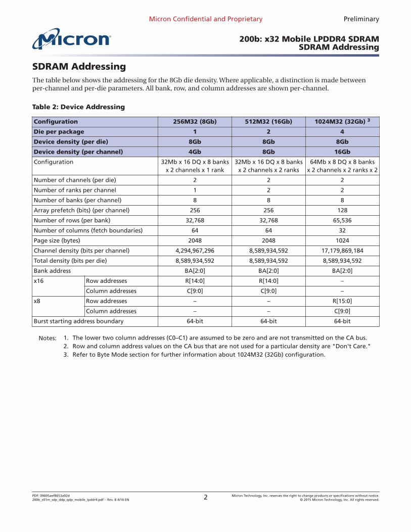
Part Number Ordering Information
Figure 1: Part Number Chart
MT 53 B 256M32 D1 NP -062 WT :C
Micron Technology
Product Family53 = Mobile LPDDR4 SDRAM
Operating VoltageB = 1.1V
Configuration256M32 = 256 Meg x 32512M32 = 512 Meg x 321024M32 = 1024 Meg x 32
AddressingD1 = LPDDR4, 1 dieD2 = LPDDR4, 2 dieD4 = LPDDR4, 4 die
Design Revision:C = Third generation
Operating TemperatureWT = –30°C to +85°C
Cycle Time–062 = 625ps,
tCK RL = 32/36 (x8 device)
tCK RL = 28/32 (x16 device)
Package CodesNP = 200-ball WFBGA (Height 0.80mm max) NQ = 200-ball VFBGA (Height 0.95mm max)
FBGA Part Marking Decoder
Due to space limitations, FBGA-packaged components have an abbreviated part marking that is different from thepart number. Micron’s FBGA part marking decoder is available at www.micron.com/decoder.
In timing diagrams, “CMD” is used as an indicator only. Actual signals occur on CA[5:0].
VREF indicates VREFCA and VREFDQ.
Micron Confidential and Proprietary Preliminary
200b: x32 Mobile LPDDR4 SDRAMPart Number Ordering Information
PDF: 09005aef8653a92d200b_z01m_sdp_ddp_qdp_mobile_lpddr4.pdf – Rev. B 4/16 EN 3 Micron Technology, Inc. reserves the right to change products or specifications without notice.
© 2015 Micron Technology, Inc. All rights reserved.
ContentsGeneral Description ....................................................................................................................................... 17
General Notes ............................................................................................................................................ 17Package Block Diagrams ................................................................................................................................. 18Ball Assignments and Descriptions ................................................................................................................. 21Package Dimensions ....................................................................................................................................... 23MR0, MR[6:3], MR8, MR13 Readout ................................................................................................................. 25IDD Parameters ............................................................................................................................................... 26Functional Description ................................................................................................................................... 28Monolithic Device Addressing ......................................................................................................................... 28Simplified Bus Interface State Diagram ............................................................................................................ 32Power-Up and Initialization ............................................................................................................................ 33
Voltage Ramp ............................................................................................................................................. 34Reset Initialization with Stable Power .......................................................................................................... 36
Power-Off Sequence ....................................................................................................................................... 37Controlled Power-Off .................................................................................................................................. 37Uncontrolled Power-Off .............................................................................................................................. 37
Mode Registers ............................................................................................................................................... 38Mode Register Assignments and Definitions ................................................................................................ 38
Commands and Timing .................................................................................................................................. 64Truth Tables ................................................................................................................................................... 64ACTIVATE Command ..................................................................................................................................... 67Read and Write Access Modes ......................................................................................................................... 68Preamble and Postamble ................................................................................................................................ 69Burst READ Operation .................................................................................................................................... 72
Read Timing ............................................................................................................................................... 74tLZ(DQS), tLZ(DQ), tHZ(DQS), tHZ(DQ) Calculation ..................................................................................... 74tLZ(DQS) and tHZ(DQS) Calculation for ATE (Automatic Test Equipment) .................................................... 75tLZ(DQ) and tHZ(DQ) Calculation for ATE (Automatic Test Equipment) ........................................................ 76
Burst WRITE Operation .................................................................................................................................. 78Write Timing .............................................................................................................................................. 80tWPRE Calculation for ATE (Automatic Test Equipment) .............................................................................. 81tWPST Calculation for ATE (Automatic Test Equipment) ............................................................................... 81
MASK WRITE Operation ................................................................................................................................. 82Mask Write Timing Constraints for BL16 ...................................................................................................... 84
Data Mask and Data Bus Inversion (DBI[DC]) Function ................................................................................... 86Preamble and Postamble Behavior .................................................................................................................. 90
Preamble, Postamble Behavior in READ-To-READ Operations ...................................................................... 90READ to READ Operations – Seamless ......................................................................................................... 90READ to READ Operations – Consecutive .................................................................................................... 91Write to Write Operations – Seamless .......................................................................................................... 98Write to Write Operations – Consecutive ..................................................................................................... 101
PRECHARGE Operation ................................................................................................................................. 105Burst Read Operation Followed by Precharge .............................................................................................. 105Burst Write Followed by Precharge ............................................................................................................. 106
Auto Precharge .............................................................................................................................................. 107Burst READ With Auto Precharge ............................................................................................................... 107Burst WRITE With Auto Precharge .............................................................................................................. 108RAS Lock Function .................................................................................................................................... 112Delay time from Write to Read with Auto Precharge .................................................................................... 113
REFRESH Command ..................................................................................................................................... 114
Micron Confidential and Proprietary Preliminary
200b: x32 Mobile LPDDR4 SDRAMPart Number Ordering Information
PDF: 09005aef8653a92d200b_z01m_sdp_ddp_qdp_mobile_lpddr4.pdf – Rev. B 4/16 EN 4 Micron Technology, Inc. reserves the right to change products or specifications without notice.
© 2015 Micron Technology, Inc. All rights reserved.
Refresh Requirement ..................................................................................................................................... 119SELF REFRESH Operation .............................................................................................................................. 120
Self Refresh Entry and Exit ......................................................................................................................... 120Power-Down Entry and Exit During Self Refresh ......................................................................................... 121Command Input Timing After Power Down Exit .......................................................................................... 122Self Refresh Abort ...................................................................................................................................... 123MRR, MRW, MPC Command During tXSR, tRFC .......................................................................................... 123
Power-Down Mode ........................................................................................................................................ 126Power-Down Entry and Exit ....................................................................................................................... 126
Input Clock Stop and Frequency Change ........................................................................................................ 136Clock Frequency Change – CKE LOW ......................................................................................................... 136Clock Stop – CKE LOW ............................................................................................................................... 136Clock Frequency Change – CKE HIGH ........................................................................................................ 136Clock Stop – CKE HIGH ............................................................................................................................. 137
MODE REGISTER READ Operation ................................................................................................................ 138MRR after Read and Write Command ......................................................................................................... 139MRR after Power-Down Exit ....................................................................................................................... 141
MODE REGISTER WRITE ............................................................................................................................... 142Mode Register Write States ......................................................................................................................... 142
VREF Current Generator (VRCG) ..................................................................................................................... 144VREF Training ................................................................................................................................................. 146
VREF(CA) Training ........................................................................................................................................ 146VREF(DQ) Training ....................................................................................................................................... 151
Command Bus Training ................................................................................................................................. 156Command Bus Training Mode .................................................................................................................... 156Training Sequence for Single-Rank Systems ................................................................................................ 157Training Sequence for Multiple-Rank Systems ............................................................................................ 158Relation between CA Input pin DQ Output pin ........................................................................................... 159
Write Leveling ............................................................................................................................................... 163Mode Register Write-WR Leveling Mode ..................................................................................................... 163Write-Leveling Procedure: .......................................................................................................................... 163Input Clock Frequency Stop and Change .................................................................................................... 164
MULTIPURPOSE Operation ........................................................................................................................... 167Read DQ Calibration Training ........................................................................................................................ 172
Read DQ Calibration Procedure ................................................................................................................. 172DQ Read Training Example ........................................................................................................................ 174MPC of Read DQ Calibration after Power-Down Exit ................................................................................... 175
Write Training ............................................................................................................................................... 176Internal Interval Timer .............................................................................................................................. 181DQS Interval Oscillator Matching Error ...................................................................................................... 183OSC Count Readout Time .......................................................................................................................... 184
Thermal Offset .............................................................................................................................................. 186Temperature Sensor ...................................................................................................................................... 186ZQ Calibration ............................................................................................................................................... 187
ZQCAL Reset ............................................................................................................................................. 188Multichannel Considerations ..................................................................................................................... 189ZQ External Resistor, Tolerance, and Capacitive Loading ............................................................................. 189
Frequency Set Points ..................................................................................................................................... 190Frequency set point update Timing ............................................................................................................ 191
Pull-Up and Pull-Down Characteristics and Calibration .................................................................................. 195On-Die Termination for the Command/Address Bus ....................................................................................... 196
ODT Mode Register and ODT State Table .................................................................................................... 196
Micron Confidential and Proprietary Preliminary
200b: x32 Mobile LPDDR4 SDRAMPart Number Ordering Information
PDF: 09005aef8653a92d200b_z01m_sdp_ddp_qdp_mobile_lpddr4.pdf – Rev. B 4/16 EN 5 Micron Technology, Inc. reserves the right to change products or specifications without notice.
© 2015 Micron Technology, Inc. All rights reserved.
ODT Mode Register and ODT Characteristics ............................................................................................. 197ODT for CA Update Time ........................................................................................................................... 199
DQ On-Die Termination ................................................................................................................................ 199Output Driver and Termination Register Temperature and Voltage Sensitivity .............................................. 202ODT Mode Register ................................................................................................................................... 203Asynchronous ODT ................................................................................................................................... 203DQ ODT During Power-Down and Self Refresh Modes ................................................................................ 205ODT During Write Leveling Mode .............................................................................................................. 205
TRR Mode – Target Row Refresh ..................................................................................................................... 206TRR Mode Operation ................................................................................................................................. 206
Post-Package Repair ...................................................................................................................................... 208Failed Row Address Repair ......................................................................................................................... 208
Read Preamble Training ................................................................................................................................. 210Electrical Specifications ................................................................................................................................. 211
Absolute Maximum Ratings ....................................................................................................................... 211AC and DC Operating Conditions ................................................................................................................... 211AC and DC Input Measurement Levels ........................................................................................................... 213
Input Levels for CKE .................................................................................................................................. 213Differential Input Voltage for CK ................................................................................................................ 213Peak Voltage Calculation Method ............................................................................................................... 214Single-Ended Input Voltage for Clock ......................................................................................................... 214Differential Input Slew Rate Definition for Clock ......................................................................................... 215Differential Input Cross-Point Voltage ........................................................................................................ 217Differential Input Voltage for DQS .............................................................................................................. 217Peak Voltage Calculation Method ............................................................................................................... 218Single-Ended Input Voltage for DQS ........................................................................................................... 219Differential Input Slew Rate Definition for DQS .......................................................................................... 220Differential Input Cross-Point Voltage ........................................................................................................ 221Input Levels for ODT ................................................................................................................................. 222
AC and DC Output Measurement Levels ......................................................................................................... 222Single-Ended Output Slew Rate .................................................................................................................. 222Differential Output Slew Rate ..................................................................................................................... 223Overshoot and Undershoot Specifications .................................................................................................. 224
Driver Output Timing Reference Load ............................................................................................................ 225LVSTL I/O System .......................................................................................................................................... 225Input/Output Capacitance ............................................................................................................................. 227IDD Specification Parameters and Test Conditions ........................................................................................... 228
IDD Specifications ...................................................................................................................................... 232AC Timing ..................................................................................................................................................... 234CA Rx Voltage and Timing .............................................................................................................................. 244DQ Tx Voltage and Timing ............................................................................................................................. 247
DRAM Data Timing ................................................................................................................................... 247DQ Rx Voltage and Timing ............................................................................................................................. 248Clock Specification ........................................................................................................................................ 251
tCK(abs), tCH(abs), and tCL(abs) ................................................................................................................ 252Clock Period Jitter .......................................................................................................................................... 252
Clock Period Jitter Effects on Core Timing Parameters ................................................................................. 252Cycle Time Derating for Core Timing Parameters ........................................................................................ 253Clock Cycle Derating for Core Timing Parameters ....................................................................................... 253Clock Jitter Effects on Command/Address Timing Parameters ..................................................................... 253Clock Jitter Effects on READ Timing Parameters .......................................................................................... 253Clock Jitter Effects on WRITE Timing Parameters ........................................................................................ 254
Micron Confidential and Proprietary Preliminary
200b: x32 Mobile LPDDR4 SDRAMPart Number Ordering Information
PDF: 09005aef8653a92d200b_z01m_sdp_ddp_qdp_mobile_lpddr4.pdf – Rev. B 4/16 EN 6 Micron Technology, Inc. reserves the right to change products or specifications without notice.
© 2015 Micron Technology, Inc. All rights reserved.
Byte Mode ..................................................................................................................................................... 255Monolithic Device Addressing (Byte Mode) ................................................................................................ 255Mode Register ........................................................................................................................................... 256
Mode Register Assignments and Definitions ........................................................................................... 256Command Truth Table ............................................................................................................................... 266Command Bus Training ............................................................................................................................. 267
Training Mode 1 .................................................................................................................................... 267Training Sequence of Mode 1 for Single-Rank Systems ............................................................................ 268Training Sequence of Mode 1 for Multi-Rank Systems ............................................................................. 269Relation between the CA Input Pin and the DQ Output Pin for Mode 1 .................................................... 270Timing for CA Training Mode 1 ............................................................................................................... 270
Read DQ Training ...................................................................................................................................... 272RD DQ Calibration Training Procedure ................................................................................................... 273DQ Read Training Example .................................................................................................................... 274
On-Die Termination .................................................................................................................................. 274ODT Control ......................................................................................................................................... 274
AC Timing ................................................................................................................................................. 276Revision History ............................................................................................................................................ 278
Rev. B– 4/16 ............................................................................................................................................... 278Rev. A – 7/15 .............................................................................................................................................. 278
Micron Confidential and Proprietary Preliminary
200b: x32 Mobile LPDDR4 SDRAMPart Number Ordering Information
PDF: 09005aef8653a92d200b_z01m_sdp_ddp_qdp_mobile_lpddr4.pdf – Rev. B 4/16 EN 7 Micron Technology, Inc. reserves the right to change products or specifications without notice.
© 2015 Micron Technology, Inc. All rights reserved.
List of FiguresFigure 1: Part Number Chart ............................................................................................................................ 3Figure 2: Single-Die, Dual-Channel Package Block Diagram ............................................................................ 18Figure 3: Dual-Die, Dual-Channel Package Block Diagram .............................................................................. 19Figure 4: Quad-Die, Dual-Channel Package Block Diagram ............................................................................. 20Figure 5: 200-Ball Dual-Channel Discrete FBGA ............................................................................................. 21Figure 6: 200-Ball WFBGA – 10mm x 14.5mm (Package Code: NP) ................................................................... 23Figure 7: 200-Ball VFBGA – 10mm x 14.5mm (Package Code: NQ) .................................................................... 24Figure 8: Simplified State Diagram ................................................................................................................. 32Figure 9: Simplified State Diagram ................................................................................................................. 33Figure 10: Voltage Ramp and Initialization Sequence ...................................................................................... 35Figure 11: ACTIVATE Command .................................................................................................................... 68Figure 12: tFAW Timing .................................................................................................................................. 68Figure 13: DQS Read Preamble and Postamble – Toggling Preamble and 0.5nCK Postamble ............................. 69Figure 14: DQS Read Preamble and Postamble – Static Preamble and 1.5nCK Postamble .................................. 69Figure 15: DQS Write Preamble and Postamble – 0.5nCK Postamble ................................................................ 70Figure 16: DQS Write Preamble and Postamble – 1.5nCK Postamble ................................................................ 71Figure 17: Burst Read Timing ......................................................................................................................... 72Figure 18: Burst Read Followed by Burst Write or Burst Mask Write .................................................................. 73Figure 19: Seamless Burst Read ...................................................................................................................... 73Figure 20: Read Timing .................................................................................................................................. 74Figure 21: tLZ(DQS) Method for Calculating Transitions and Endpoint ............................................................ 75Figure 22: tHZ(DQS) Method for Calculating Transitions and Endpoint ........................................................... 75Figure 23: tLZ(DQ) Method for Calculating Transitions and Endpoint .............................................................. 76Figure 24: tHZ(DQ) Method for Calculating Transitions and Endpoint ............................................................. 77Figure 25: Burst WRITE Operation ................................................................................................................. 78Figure 26: Burst Write Followed by Burst Read ................................................................................................ 79Figure 27: Write Timing ................................................................................................................................. 80Figure 28: Method for Calculating tWPRE Transitions and Endpoints ............................................................... 81Figure 29: Method for Calculating tWPST Transitions and Endpoints ............................................................... 81Figure 30: Mask Write Command - Same Bank ............................................................................................... 82Figure 31: Masked Write Command - Different Bank ...................................................................................... 83Figure 32: MASKED WRITE Command with Write DBI Enabled; DM Enabled .................................................. 88Figure 33: WRITE Command with Write DBI Enabled; DM Disabled ................................................................ 89Figure 34: READ Operations: tCCD = Min, Preamble = Toggle, 1.5nCK Postamble ............................................. 90Figure 35: Seamless READ: tCCD = Min +1, Preamble = Toggle, 1.5nCK Postamble ........................................... 91Figure 36: Consecutive READ: tCCD = Min +1, Preamble = Toggle, 0.5nCK Postamble ....................................... 91Figure 37: Consecutive READ: tCCD = Min +1, Preamble = Static, 1.5nCK Postamble ........................................ 92Figure 38: Consecutive READ: tCCD = Min +1, Preamble = Static, 0.5nCK Postamble ........................................ 92Figure 39: Consecutive READ: tCCD = Min + 2, Preamble = Toggle, 1.5nCK Postamble ...................................... 93Figure 40: Consecutive READ: tCCD = Min + 2, Preamble = Toggle, 0.5nCK Postamble ...................................... 94Figure 41: Consecutive READ: tCCD = Min + 2, Preamble = Static, 1.5nCK Postamble ....................................... 94Figure 42: Consecutive READ: tCCD = Min + 2, Preamble = Static, 0.5nCK Postamble ....................................... 95Figure 43: Consecutive READ: tCCD = Min + 3, Preamble = Toggle, 1.5nCK Postamble ...................................... 96Figure 44: Consecutive READ: tCCD = Min + 3, Preamble = Toggle, 0.5nCK Postamble ...................................... 96Figure 45: Consecutive READ: tCCD = Min + 3, Preamble = Static, 1.5nCK Postamble ....................................... 97Figure 46: Consecutive READ: tCCD = Min + 3, Preamble = Static, 0.5nCK Postamble ....................................... 97Figure 47: Seamless Write: tCCD = Min, 0.5nCK Postamble .............................................................................. 98Figure 48: Seamless Write: tCCD = Min, 1.5nCK Postamble, 533MHz < Clock Frequency ≤ 800MHz, ODT Worst
Timing Case ............................................................................................................................................... 99Figure 49: Seamless Write: tCCD = Min, 1.5nCK Postamble ............................................................................. 100
Micron Confidential and Proprietary Preliminary
200b: x32 Mobile LPDDR4 SDRAMPart Number Ordering Information
PDF: 09005aef8653a92d200b_z01m_sdp_ddp_qdp_mobile_lpddr4.pdf – Rev. B 4/16 EN 8 Micron Technology, Inc. reserves the right to change products or specifications without notice.
© 2015 Micron Technology, Inc. All rights reserved.
Figure 50: Consecutive Write: tCCD = Min + 1, 0.5nCK Postamble ................................................................... 101Figure 51: Consecutive Write: tCCD = Min + 1, 1.5nCK Postamble ................................................................... 101Figure 52: Consecutive Write: tCCD = Min + 2, 0.5nCK Postamble ................................................................... 102Figure 53: Consecutive Write: tCCD = Min + 2, 1.5nCK Postamble ................................................................... 102Figure 54: Consecutive Write: tCCD = Min + 3, 0.5nCK Postamble ................................................................... 103Figure 55: Consecutive Write: tCCD = Min + 3, 1.5nCK Postamble ................................................................... 104Figure 56: Consecutive Write: tCCD = Min + 4, 1.5nCK Postamble ................................................................... 104Figure 57: Burst Read Followed by Precharge – BL16, Toggling Preamble, 0.5nCK Postamble ........................... 106Figure 58: Burst Read Followed by Precharge – BL32, 2tCK, 0.5nCK Postamble ................................................ 106Figure 59: Burst WRITE Followed by PRECHARGE – BL16, 2nCK Preamble, 0.5nCK Postamble ........................ 107Figure 60: Burst READ With Auto Precharge – BL16, Non-Toggling Preamble, 0.5nCK Postamble ..................... 108Figure 61: Burst READ With Auto Precharge – BL32, Toggling Preamble, 1.5nCK Postamble ............................. 108Figure 62: Burst WRITE With Auto Precharge – BL16, 2 nCK Preamble, 0.5nCK Postamble ................................ 109Figure 63: Command Input Timing with RAS Lock ......................................................................................... 113Figure 64: Delay Time from Write to Read with Auto Precharge ...................................................................... 113Figure 65: All-Bank REFRESH Operation ....................................................................................................... 116Figure 66: Per Bank REFRESH Operation ....................................................................................................... 117Figure 67: Postponing REFRESH Commands (Example) ................................................................................. 119Figure 68: Pulling In REFRESH Commands (Example) ................................................................................... 119Figure 69: Self Refresh Entry/Exit Timing ...................................................................................................... 121Figure 70: Self Refresh Entry/Exit Timing with Power-Down Entry/Exit .......................................................... 122Figure 71: Command Input Timings after Power-Down Exit during Self Refresh .............................................. 123Figure 72: MRR, MRW, and MPC Commands Issuing Timing During tXSR ....................................................... 124Figure 73: MRR, MRW, and MPC Commands Issuing Timing During tRFC ...................................................... 125Figure 74: Basic Power-Down Entry and Exit Timing ...................................................................................... 127Figure 75: Read and Read with Auto Precharge to Power-Down Entry ............................................................. 128Figure 76: Write and Mask Write to Power-Down Entry .................................................................................. 129Figure 77: Write with Auto Precharge and Mask Write with Auto Precharge to Power-Down Entry .................... 130Figure 78: Refresh Entry to Power-Down Entry .............................................................................................. 131Figure 79: Activate Command to Power-Down Entry ...................................................................................... 131Figure 80: Precharge Command to Power-Down Entry ................................................................................... 132Figure 81: Mode Register Read to Power-Down Entry ..................................................................................... 133Figure 82: Mode Register Write to Power-Down Entry .................................................................................... 134Figure 83: Multi Purpose Command for Start ZQ Calibration to Power-Down Entry ......................................... 135Figure 84: MODE REGISTER READ Operation ............................................................................................... 139Figure 85: READ to MRR Timing ................................................................................................................... 140Figure 86: Write to MRR Timing .................................................................................................................... 141Figure 87: MRR Following Power-Down ......................................................................................................... 142Figure 88: MODE REGISTER WRITE Timing .................................................................................................. 142Figure 89: VRCG Enable Timing .................................................................................................................... 145Figure 90: VRCG Disable Timing ................................................................................................................... 145Figure 91: VREF Operating Range (VREF,max, VREF,min) ....................................................................................... 146Figure 92: VREF Set-Point Tolerance and Step Size .......................................................................................... 147Figure 93: tVref for Short, Middle and Long Timing Diagram ........................................................................... 148Figure 94: VREF(CA) Single-Step Increment ...................................................................................................... 148Figure 95: VREF(CA) Single-Step Decrement ..................................................................................................... 149Figure 96: VREF(CA) Full Step from VREF,min to VREF,max ...................................................................................... 149Figure 97: VREF(CA) Full Step from VREF,max to VREF,min ...................................................................................... 149Figure 98: VREF Operating Range (VREF,max, VREF,min) ....................................................................................... 151Figure 99: VREF Set Tolerance and Step Size .................................................................................................... 152Figure 100: VREF(DQ) Transition Time for Short, Middle, or Long Changes ........................................................ 153Figure 101: VREF(DQ) Single-Step Size Increment ............................................................................................. 153
Micron Confidential and Proprietary Preliminary
200b: x32 Mobile LPDDR4 SDRAMPart Number Ordering Information
PDF: 09005aef8653a92d200b_z01m_sdp_ddp_qdp_mobile_lpddr4.pdf – Rev. B 4/16 EN 9 Micron Technology, Inc. reserves the right to change products or specifications without notice.
© 2015 Micron Technology, Inc. All rights reserved.
Figure 102: VREF(DQ) Single-Step Size Decrement ............................................................................................ 154Figure 103: VREF(DQ) Full Step from VREF,min to VREF,max ................................................................................... 154Figure 104: VREF(DQ) Full Step from VREF,max to VREF,min ................................................................................... 154Figure 105: Command Bus Training Mode Entry – CA Training Pattern I/O With V REF(CA) Value Update ............ 159Figure 106: Consecutive VREF(CA) Value Update .............................................................................................. 160Figure 107: Command Bus Training Mode Exit With Valid Command ............................................................. 161Figure 108: Command Bus Training Mode Exit With Power-Down Entry ......................................................... 162Figure 109: Write-Leveling Timing – tDQSL (MAX) ......................................................................................... 164Figure 110: Write Leveling Timing – tDQSL (MIN) .......................................................................................... 164Figure 111: Clock Stop and Timing During Write Leveling .............................................................................. 165Figure 112: DQS_t/DQS_c to CK_t/CK_t Timings at the Pins Referenced from the Internal Latch ..................... 166Figure 113: WR-FIFO – tWPRE = 2nCK, tWPST = 0.5nCK ................................................................................. 168Figure 114: RD-FIFO – tWPRE = 2nCK, tWPST = 0.5nCK, tRPRE = Toggling, tRPST = 1.5nCK .............................. 169Figure 115: RD-FIFO – tRPRE = Toggling, tRPST = 1.5nCK ............................................................................... 170Figure 116: DQ Read Training Timing: Read to Read DQ Calibration ............................................................... 173Figure 117: DQ Read Training Timing: Read DQ Calibration to Read DQ Calibration/Read .............................. 173Figure 118: MPC Read DQ Calibration Following Power-Down State ............................................................... 175Figure 119: WRITE to MPC [WRITE FIFO] Operation Timing .......................................................................... 177Figure 120: MPC [WRITE FIFO] to MPC [READ FIFO] Timing ......................................................................... 178Figure 121: MPC [READ FIFO] to Read Timing ............................................................................................... 179Figure 122: MPC [WRITE FIFO] with DQ ODT Timing .................................................................................... 180Figure 123: Power Down Exit to MPC [WRITE FIFO] Timing ........................................................................... 181Figure 124: Interval Oscillator Offset – OSCoffset ............................................................................................. 183Figure 125: In case of DQS Interval Oscillator is stopped by MPC Command ................................................... 184Figure 126: In case of DQS Interval Oscillator is stopped by DQS interval timer ............................................... 185Figure 127: Temperature Sensor Timing ........................................................................................................ 187Figure 128: ZQCal Timing ............................................................................................................................. 188Figure 129: Frequency Set Point Switching Timing ......................................................................................... 192Figure 130: Training for Two Frequency Set Points ......................................................................................... 194Figure 131: Example of Switching Between Two Trained Frequency Set Points ................................................ 194Figure 132: Example of Switching to a Third Trained Frequency Set Point ....................................................... 195Figure 133: ODT for CA ................................................................................................................................. 196Figure 134: ODT for CA Setting Update Timing in 4-Clock Cycle Command .................................................... 199Figure 135: Functional Representation of DQ ODT ........................................................................................ 200Figure 136: Asynchronous ODTon/ODToff Timing ......................................................................................... 204Figure 137: Target Row Refresh Mode ............................................................................................................ 207Figure 138: Post-Package Repair Timing ........................................................................................................ 209Figure 139: Read Preamble Training .............................................................................................................. 210Figure 140: AC Input Timing Definition ......................................................................................................... 213Figure 141: CK Differential Input Voltage ....................................................................................................... 213Figure 142: Definition of Differential Clock Peak Voltage ................................................................................ 214Figure 143: Clock Single-Ended Input Voltage ................................................................................................ 215Figure 144: Differential Input Slew Rate Definition for CK_t, CK_c .................................................................. 216Figure 145: Vix Definition (Clock) .................................................................................................................. 217Figure 146: DQS Differential Input Voltage .................................................................................................... 218Figure 147: Definition of Differential DQS Peak Voltage .................................................................................. 219Figure 148: DQS Single-Ended Input Voltage ................................................................................................. 219Figure 149: Differential Input Slew Rate Definition for DQS_t, DQS_c ............................................................. 220Figure 150: Vix Definition (DQS) .................................................................................................................... 221Figure 151: Single-Ended Output Slew Rate Definition ................................................................................... 223Figure 152: Differential Output Slew Rate Definition ...................................................................................... 224Figure 153: Overshoot and Undershoot Definition ......................................................................................... 225
Micron Confidential and Proprietary Preliminary
200b: x32 Mobile LPDDR4 SDRAMPart Number Ordering Information
PDF: 09005aef8653a92d200b_z01m_sdp_ddp_qdp_mobile_lpddr4.pdf – Rev. B 4/16 EN 10 Micron Technology, Inc. reserves the right to change products or specifications without notice.
© 2015 Micron Technology, Inc. All rights reserved.
Figure 154: Driver Output Timing Reference Load ......................................................................................... 225Figure 155: LVSTL I/O Cell ............................................................................................................................ 226Figure 156: Pull-Up Calibration ..................................................................................................................... 227Figure 157: tCMDCKE Timing ....................................................................................................................... 238Figure 158: tESCKE Timing ........................................................................................................................... 241Figure 159: CA Receiver (Rx) Mask ................................................................................................................ 244Figure 160: Across Pin VREF CA Voltage Variation ............................................................................................ 244Figure 161: CA Timings at the DRAM Pins ..................................................................................................... 245Figure 162: CA tcIPW and SRIN_cIVW Definition (for Each Input Pulse) .......................................................... 245Figure 163: CA VIHL_AC Definition (for Each Input Pulse) ................................................................................ 245Figure 164: Read Data Timing Definitions – tQH and tDQSQ Across DQ Signals per DQS Group ....................... 247Figure 165: DQ Receiver (Rx) Mask ................................................................................................................ 248Figure 166: Across Pin VREF DQ Voltage Variation ........................................................................................... 248Figure 167: DQ-to-DQS tDQS2DQ and tDQDQ .............................................................................................. 249Figure 168: DQ tDIPW and SRIN_dIVW Definition for Each Input Pulse .......................................................... 250Figure 169: DQ VIHL(AC) Definition (for Each Input Pulse) ............................................................................... 250Figure 170: Entering CBT Mode and CA Training Pattern (Input and Output) .................................................. 270Figure 171: Exiting CBT Mode with Valid Command ...................................................................................... 271Figure 172: Exiting CBT Mode with Power Down Entry ................................................................................... 272Figure 173: DQ Read Training Timing ............................................................................................................ 274
Micron Confidential and Proprietary Preliminary
200b: x32 Mobile LPDDR4 SDRAMPart Number Ordering Information
PDF: 09005aef8653a92d200b_z01m_sdp_ddp_qdp_mobile_lpddr4.pdf – Rev. B 4/16 EN 11 Micron Technology, Inc. reserves the right to change products or specifications without notice.
© 2015 Micron Technology, Inc. All rights reserved.
List of TablesTable 1: Key Timing Parameters ....................................................................................................................... 1Table 2: Device Addressing .............................................................................................................................. 2Table 3: Ball/Pad Descriptions ....................................................................................................................... 22Table 4: Mode Register Contents .................................................................................................................... 25Table 5: IDD Parameters – Single-Die .............................................................................................................. 26Table 6: IDD6 Full-Array Self Refresh Current ................................................................................................... 27Table 7: Monolithic Device Addressing – 2 Channels per Die ........................................................................... 29Table 8: Monolithic Device Addressing – 1 Channel per Die ............................................................................. 30Table 9: Mode Register Default Settings .......................................................................................................... 34Table 10: Voltage Ramp Conditions ................................................................................................................ 34Table 11: Initialization Timing Parameters ...................................................................................................... 36Table 12: Reset Timing Parameter .................................................................................................................. 37Table 13: Power Supply Conditions ................................................................................................................ 37Table 14: Power-Off Timing ............................................................................................................................ 38Table 15: Mode Register Assignments ............................................................................................................. 38Table 16: MR0 Device Feature 0 (MA[7:0] = 00h) .............................................................................................. 39Table 17: MR0 Op-Code Bit Definitions .......................................................................................................... 39Table 18: MR1 Device Feature 1 (MA[7:0] = 01h) .............................................................................................. 40Table 19: MR1 Op-Code Bit Definitions .......................................................................................................... 40Table 20: Burst Sequence ............................................................................................................................... 42Table 21: MR2 Device Feature 2 (MA[7:0] = 02h) .............................................................................................. 43Table 22: MR2 Op-Code Bit Definitions .......................................................................................................... 43Table 23: Frequency Ranges for RL, WL, nWR and nRTP Settings ..................................................................... 45Table 24: MR3 I/O Configuration 1 (MA[7:0] = 03h) ......................................................................................... 45Table 25: MR3 Op-Code Bit Definitions .......................................................................................................... 46Table 26: MR4 Device Temperature (MA[7:0] = 04h) ........................................................................................ 47Table 27: MR4 Op-Code Bit Definitions .......................................................................................................... 47Table 28: MR5 Basic Configuration 1 (MA[7:0] = 05h) ...................................................................................... 48Table 29: MR5 Op-Code Bit Definitions .......................................................................................................... 48Table 30: MR6 Basic Configuration 2 (MA[7:0] = 06h) ...................................................................................... 48Table 31: MR6 Op-Code Bit Definitions .......................................................................................................... 48Table 32: MR7 Basic Configuration 3 (MA[7:0] = 07h) ...................................................................................... 48Table 33: MR7 Op-Code Bit Definitions .......................................................................................................... 48Table 34: MR8 Basic Configuration 4 (MA[7:0] = 08h) ...................................................................................... 49Table 35: MR8 Op-Code Bit Definitions .......................................................................................................... 49Table 36: MR9 Test Mode (MA[7:0] = 09h) ....................................................................................................... 49Table 37: MR9 Op-Code Definitions ............................................................................................................... 49Table 38: MR10 Calibration (MA[7:0] = 0Ah) ................................................................................................... 49Table 39: MR10 Op-Code Bit Definitions ........................................................................................................ 50Table 40: MR11 ODT Control (MA[7:0] = 0Bh) ................................................................................................. 50Table 41: MR11 Op-Code Bit Definitions ........................................................................................................ 50Table 42: MR12 Register Information (MA[7:0] = 0Ch) ..................................................................................... 51Table 43: MR12 Op-Code Bit Definitions ........................................................................................................ 51Table 44: MR13 Register Control (MA[7:0] = 0Dh) ............................................................................................ 51Table 45: MR13 Op-Code Bit Definition .......................................................................................................... 52Table 46: Mode Register 14 (MA[7:0] = 0Eh) .................................................................................................... 53Table 47: MR14 Op-Code Bit Definition .......................................................................................................... 53Table 48: VREF Setting for Range[0] and Range[1] ............................................................................................. 54Table 49: MR15 Register Information (MA[7:0] = 0Fh) ..................................................................................... 55Table 50: MR15 Op-code Bit Definition .......................................................................................................... 55
Micron Confidential and Proprietary Preliminary
200b: x32 Mobile LPDDR4 SDRAMPart Number Ordering Information
PDF: 09005aef8653a92d200b_z01m_sdp_ddp_qdp_mobile_lpddr4.pdf – Rev. B 4/16 EN 12 Micron Technology, Inc. reserves the right to change products or specifications without notice.
© 2015 Micron Technology, Inc. All rights reserved.
Table 51: MR15 Invert Register Pin Mapping ................................................................................................... 55Table 52: MR16 PASR Bank Mask (MA[7:0] = 010h) .......................................................................................... 55Table 53: MR16 Op-Code Bit Definitions ........................................................................................................ 55Table 54: MR17 PASR Segment Mask (MA[7:0] = 11h) ...................................................................................... 56Table 55: MR17 PASR Segment Mask Definitions ............................................................................................ 56Table 56: MR17 PASR Segment Mask .............................................................................................................. 56Table 57: MR18 Register Information (MA[7:0]=12h) ....................................................................................... 57Table 58: MR18 LSB DQS Oscillator Count ...................................................................................................... 57Table 59: MR19 Register Information (MA[7:0] = 13h) ..................................................................................... 57Table 60: MR19 DQS Oscillator Count ............................................................................................................ 57Table 61: MR20 Register Information (MA[7:0] = 14h) ..................................................................................... 58Table 62: MR20 Register Information ............................................................................................................. 58Table 63: MR20 Invert Register Pin Mapping ................................................................................................... 58Table 64: MR21 Register Information (MA[7:0] = 15h) ..................................................................................... 58Table 65: MR22 Register Information (MA[7:0] = 16h) ..................................................................................... 58Table 66: MR22 Register Information ............................................................................................................. 59Table 67: MR23 Register Information (MA[7:0] = 17h) ..................................................................................... 60Table 68: MR23 Register Information ............................................................................................................. 60Table 69: MR24 Register Information (MA[7:0] = 18h) ..................................................................................... 60Table 70: MR24 Register Information ............................................................................................................. 61Table 71: MR25 Register Information (MA[7:0] = 19h) ..................................................................................... 61Table 72: MR25 Register Information ............................................................................................................. 61Table 73: MR26:31 Register Information (MA[7:0] = 1Ah–1Fh) ......................................................................... 62Table 74: MR32 Register Information (MA[7:0] = 20h) ..................................................................................... 62Table 75: MR32 Register Information ............................................................................................................. 62Table 76: DQ Read Calibration Bit Order and Inversion Example – MR32 = 1Ch, MR40 = 59h, MR15 = MR20 =
55h ............................................................................................................................................................ 62Table 77: MR33:39 Register Information (MA[7:0] = 21h–27h) .......................................................................... 63Table 78: MR40 Register Information (MA[7:0] = 28h) ..................................................................................... 63Table 79: MR40 Register Information ............................................................................................................. 63Table 80: MR41:47 Register Information (MA[7:0] = 29h–2Fh) .......................................................................... 64Table 81: MR48:63 Register Information (MA[7:0] = 30h–3Fh) .......................................................................... 64Table 82: Command Truth Table .................................................................................................................... 64Table 83: Reference Voltage for tLZ(DQS), tHZ(DQS) Timing Measurements ..................................................... 76Table 84: Reference Voltage for tLZ(DQ), tHZ(DQ) Timing Measurements ........................................................ 77Table 85: Method for Calculating tWPRE Transitions and Endpoints ................................................................ 81Table 86: Reference Voltage for tWPST Timing Measurements ......................................................................... 82Table 87: Same Bank (ODT disabled) .............................................................................................................. 84Table 88: Different Bank (ODT disabled) ........................................................................................................ 84Table 89: Same Bank (ODT enabled) .............................................................................................................. 85Table 90: Different Bank (ODT enabled) ......................................................................................................... 85Table 91: Function Behavior of DMI Signal During WRITE, MASKED WRITE, and READ Operations ................. 86Table 92: Precharge Bank Selection ............................................................................................................... 105Table 93: Timing Between Commands (PRECHARGE and AUTO PRECHARGE): DQ ODT is Disable ................. 109Table 94: Timing Between Commands (PRECHARGE and AUTO PRECHARGE): DQ ODT is Enable ................. 112Table 95: Bank and Refresh Counter Increment Behavior ............................................................................... 114Table 96: REFRESH Command Timing Constraints ........................................................................................ 116Table 97: Legacy REFRESH Command Timing Constraints ............................................................................. 118Table 98: Modified REFRESH Command Timing Constraints ......................................................................... 118Table 99: Refresh Requirement Parameters .................................................................................................... 119Table 100: MRR ............................................................................................................................................ 138Table 101: Truth Table for MRR and MRW ..................................................................................................... 143
Micron Confidential and Proprietary Preliminary
200b: x32 Mobile LPDDR4 SDRAMPart Number Ordering Information
PDF: 09005aef8653a92d200b_z01m_sdp_ddp_qdp_mobile_lpddr4.pdf – Rev. B 4/16 EN 13 Micron Technology, Inc. reserves the right to change products or specifications without notice.
© 2015 Micron Technology, Inc. All rights reserved.
Table 102: MRR/MRW Timing Constraints: DQ ODT is Disable ...................................................................... 143Table 103: MRR/MRW Timing Constraints: DQ ODT is Enable ....................................................................... 144Table 104: VRCG Enable/Disable Timing ....................................................................................................... 145Table 105: Internal VREF(CA) Specifications ..................................................................................................... 150Table 106: Internal VREF(DQ) Specifications .................................................................................................... 155Table 107: Mapping MR12 Op Code and DQ Numbers ................................................................................... 157Table 108: Mapping CA Input pin DQ Output pin .......................................................................................... 159Table 109: Write Leveling Timing Parameters ................................................................................................. 165Table 110: Write Leveling Setup and Hold Timing .......................................................................................... 165Table 111: MPC Command Definition ........................................................................................................... 167Table 112: MPC Commands .......................................................................................................................... 168Table 113: Timing Constraints for Training Commands .................................................................................. 170Table 114: Invert Mask Assignments .............................................................................................................. 172Table 115: DQ Read Calibration Bit Ordering and Inversion Example .............................................................. 174Table 116: MR Setting vs. DMI Status ............................................................................................................. 175Table 117: MPC [WRITE FIFO] AC Timing ..................................................................................................... 181Table 118: DQS Oscillator Matching Error Specification ................................................................................. 183Table 119: AC Timing .................................................................................................................................... 185Table 120: Temperature Sensor ..................................................................................................................... 187Table 121: ZQ Calibration Parameters ........................................................................................................... 188Table 122: Mode Register Function with Two Physical Registers ...................................................................... 190Table 123: Relation Between MR Setting and DRAM Operation ...................................................................... 191Table 124: Frequency Set Point AC Timing ..................................................................................................... 192Table 125: tFC Value Mapping ....................................................................................................................... 192Table 126: tFC Value Mapping ....................................................................................................................... 193Table 127: Pull-Down Driver Characteristics – ZQ Calibration ........................................................................ 195Table 128: Pull-Up Characteristics – ZQ Calibration ....................................................................................... 195Table 129: Valid Calibration Points ................................................................................................................ 195Table 130: Command Bus ODT State ............................................................................................................. 197Table 131: ODT DC Electrical Characteristics – up to 3200 Mbps .................................................................... 197Table 132: ODT DC Electrical Characteristics – Beyond 3200 Mbps ................................................................. 198Table 133: ODT DC Electrical Characteristics – up to 3200 Mbps .................................................................... 200Table 134: ODT DC Electrical Characteristics – Beyond 3200 Mbps ................................................................. 201Table 135: Output Driver and Termination Register Sensitivity Definition ....................................................... 202Table 136: Output Driver and Termination Register Temperature and Voltage Sensitivity ................................. 202Table 137: ODTLON and ODTLOFF Latency Values .......................................................................................... 204Table 138: Termination State in Write Leveling Mode ..................................................................................... 205Table 139: Post-Package Repair Timing Parameters ........................................................................................ 209Table 140: Absolute Maximum DC Ratings .................................................................................................... 211Table 141: Recommended DC Operating Conditions ..................................................................................... 211Table 142: Input Leakage Current .................................................................................................................. 212Table 143: Input/Output Leakage Current ..................................................................................................... 212Table 144: Operating Temperature Range ...................................................................................................... 212Table 145: Input Levels ................................................................................................................................. 213Table 146: CK Differential Input Voltage ........................................................................................................ 214Table 147: Clock Single-Ended Input Voltage ................................................................................................. 215Table 148: Differential Input Slew Rate Definition for CK_t, CK_c ................................................................... 216Table 149: Differential Input Level for CK_t, CK_c .......................................................................................... 216Table 150: Differential Input Slew Rate for CK_t, CK_c .................................................................................... 216Table 151: Cross-Point Voltage for Differential Input Signals (Clock) ............................................................... 217Table 152: DQS Differential Input Voltage ...................................................................................................... 218Table 153: DQS Single-Ended Input Voltage ................................................................................................... 220
Micron Confidential and Proprietary Preliminary
200b: x32 Mobile LPDDR4 SDRAMPart Number Ordering Information
PDF: 09005aef8653a92d200b_z01m_sdp_ddp_qdp_mobile_lpddr4.pdf – Rev. B 4/16 EN 14 Micron Technology, Inc. reserves the right to change products or specifications without notice.
© 2015 Micron Technology, Inc. All rights reserved.
Table 154: Differential Input Slew Rate Definition for DQS_t, DQS_c .............................................................. 220Table 155: Differential Input Level for DQS_t, DQS_c ..................................................................................... 221Table 156: Differential Input Slew Rate for DQS_t, DQS_c ............................................................................... 221Table 157: Cross-Point Voltage for Differential Input Signals (DQS) ................................................................ 222Table 158: Input Levels ................................................................................................................................. 222Table 159: Single-Ended AC and DC Output Levels – ODT Enabled ................................................................. 222Table 160: Single-Ended Output Slew Rate .................................................................................................... 223Table 161: Differential Output Slew Rate ....................................................................................................... 223Table 162: AC Overshoot/Undershoot Specifications ..................................................................................... 224Table 163: Overshoot/Undershoot Specification for CKE and RESET .............................................................. 224Table 164: Input/Output Capacitance ........................................................................................................... 227Table 165: IDD Measurement Conditions ....................................................................................................... 228Table 166: CA Pattern for IDD4R ...................................................................................................................... 228Table 167: CA Pattern for IDD4W ..................................................................................................................... 229Table 168: Data Pattern for IDD4W (DBI Off) ................................................................................................... 229Table 169: Data Pattern for IDD4R (DBI Off) .................................................................................................... 230Table 170: IDD Specification Parameters and Operating Conditions ................................................................ 232Table 171: Clock Timing ............................................................................................................................... 234Table 172: Read Output Timing ..................................................................................................................... 234Table 173: Write Voltage and Timing ............................................................................................................. 236Table 174: CKE Input Timing ........................................................................................................................ 237Table 175: Command Address Input Timing .................................................................................................. 238Table 176: Boot Timing Parameters (10–55 MHz) ........................................................................................... 239Table 177: Mode Register Timing Parameters ................................................................................................. 239Table 178: Core Timing Parameters ............................................................................................................... 240Table 179: CA Bus ODT Timing ..................................................................................................................... 241Table 180: CA Bus Training Parameters .......................................................................................................... 241Table 181: Asynchronous ODT Turn On and Turn Off Timing ......................................................................... 242Table 182: Temperature Derating Parameters ................................................................................................ 242Table 183: DRAM CMD/ADR, CS ................................................................................................................... 246Table 184: DQs In Receive Mode ................................................................................................................... 250Table 185: Definitions and Calculations ........................................................................................................ 251Table 186: tCK(abs), tCH(abs), and tCL(abs) Definitions ................................................................................. 252Table 187: 2-channel Byte Mode Addressing .................................................................................................. 255Table 188: Mode Register Assignments .......................................................................................................... 256Table 189: MR0 Device Feature 0 (MA[7:0] = 00h) ........................................................................................... 257Table 190: MR0 Op-Code Bit Definitions ....................................................................................................... 257Table 191: MR1 Device Feature 1 (MA[7:0] = 01h) ........................................................................................... 258Table 192: MR1 Op-Code Bit Definitions ....................................................................................................... 258Table 193: Burst Sequence ............................................................................................................................ 259Table 194: MR2 Device Feature 2 (MA[7:0] = 02h) ........................................................................................... 260Table 195: MR2 Op-Code Bit Definitions ....................................................................................................... 260Table 196: Byte Mode Frequency Ranges for RL, WL, and nWR ....................................................................... 262Table 197: MR8 Basic Configuration 4 (MA[7:0] = 08h) ................................................................................... 262Table 198: MR8 Op-Code Bit Definitions ....................................................................................................... 262Table 199: MR11 ODT Control (MA[7:0] = 0Bh) .............................................................................................. 263Table 200: MR11 Op-Code Bit Definitions ...................................................................................................... 263Table 201: MR17 PASR Segment Mask (MA[7:0] = 11h) ................................................................................... 264Table 202: MR17 PASR Segment Mask Definitions .......................................................................................... 264Table 203: MR17 PASR Segment Mask ........................................................................................................... 264Table 204: MR22 Register Information (MA[7:0] = 16h) ................................................................................... 265Table 205: MR22 Register Information ........................................................................................................... 265
Micron Confidential and Proprietary Preliminary
200b: x32 Mobile LPDDR4 SDRAMPart Number Ordering Information
PDF: 09005aef8653a92d200b_z01m_sdp_ddp_qdp_mobile_lpddr4.pdf – Rev. B 4/16 EN 15 Micron Technology, Inc. reserves the right to change products or specifications without notice.
© 2015 Micron Technology, Inc. All rights reserved.
Table 206: Command Truth Table Change ..................................................................................................... 266Table 207: Command Bus Training Steps ....................................................................................................... 268Table 208: Mapping of CA Input Pin and DQ Output Pin ................................................................................ 270Table 209: Invert Mask Assignments .............................................................................................................. 273Table 210: DQ Read Training Output ............................................................................................................. 274Table 211: ODTLon_rd and ODTLoff_rd Latency Values (Non Target DRAM) ................................................... 275Table 212: Core AC Timing ............................................................................................................................ 276Table 213: CBT AC Timing for Mode 1 ........................................................................................................... 276Table 214: AC Timing Parameters for 2 channel x8 CBT Mode ......................................................................... 276
Micron Confidential and Proprietary Preliminary
200b: x32 Mobile LPDDR4 SDRAMPart Number Ordering Information
PDF: 09005aef8653a92d200b_z01m_sdp_ddp_qdp_mobile_lpddr4.pdf – Rev. B 4/16 EN 16 Micron Technology, Inc. reserves the right to change products or specifications without notice.
© 2015 Micron Technology, Inc. All rights reserved.
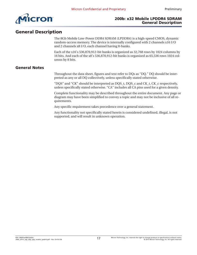
General DescriptionThe 8Gb Mobile Low-Power DDR4 SDRAM (LPDDR4) is a high-speed CMOS, dynamicrandom-access memory. The device is internally configured with 2 channels x16 I/Oand 2 channels x8 I/O, each channel having 8-banks.
Each of the x16’s 536,870,912-bit banks is organized as 32,768 rows by 1024 columns by16 bits. And each of the x8’s 536,870,912-bit banks is organized as 65,536 rows 1024 col-umns by 8 bits.
General Notes
Throughout the data sheet, figures and text refer to DQs as “DQ.” DQ should be inter-preted as any or all DQ collectively, unless specifically stated otherwise.
“DQS” and “CK” should be interpreted as DQS_t, DQS_c and CK_t, CK_c respectively,unless specifically stated otherwise. “CA” includes all CA pins used for a given density.
Complete functionality may be described throughout the entire document. Any page ordiagram may have been simplified to convey a topic and may not be inclusive of all re-quirements.
Any specific requirement takes precedence over a general statement.
Any functionality not specifically stated herein is considered undefined, illegal, is notsupported, and will result in unknown operation.
Micron Confidential and Proprietary Preliminary
200b: x32 Mobile LPDDR4 SDRAMGeneral Description
PDF: 09005aef8653a92d200b_z01m_sdp_ddp_qdp_mobile_lpddr4.pdf – Rev. B 4/16 EN 17 Micron Technology, Inc. reserves the right to change products or specifications without notice.
© 2015 Micron Technology, Inc. All rights reserved.
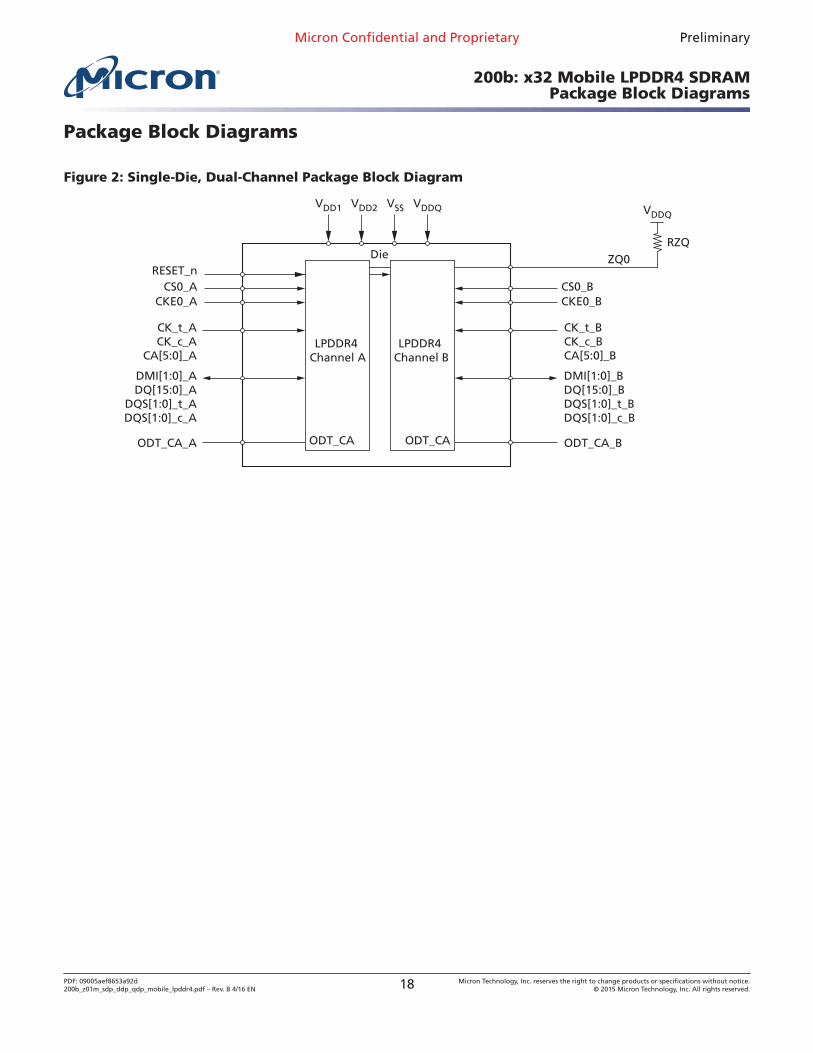
Package Block Diagrams
Figure 2: Single-Die, Dual-Channel Package Block Diagram
LPDDR4 Channel A
LPDDR4 Channel B
DieRESET_n
CS0_ACKE0_A CKE0_B
CS0_B
CK_t_ACK_c_A
CA[5:0]_A
CK_t_BCK_c_BCA[5:0]_B
DMI[1:0]_ADQ[15:0]_A
DQS[1:0]_t_ADQS[1:0]_c_A
DMI[1:0]_BDQ[15:0]_BDQS[1:0]_t_BDQS[1:0]_c_B
ODT_CA_A ODT_CA_BODT_CAODT_CA
ZQ0
VDD1 VDD2 VSS VDDQ
RZQ
VDDQ
Micron Confidential and Proprietary Preliminary
200b: x32 Mobile LPDDR4 SDRAMPackage Block Diagrams
PDF: 09005aef8653a92d200b_z01m_sdp_ddp_qdp_mobile_lpddr4.pdf – Rev. B 4/16 EN 18 Micron Technology, Inc. reserves the right to change products or specifications without notice.
© 2015 Micron Technology, Inc. All rights reserved.
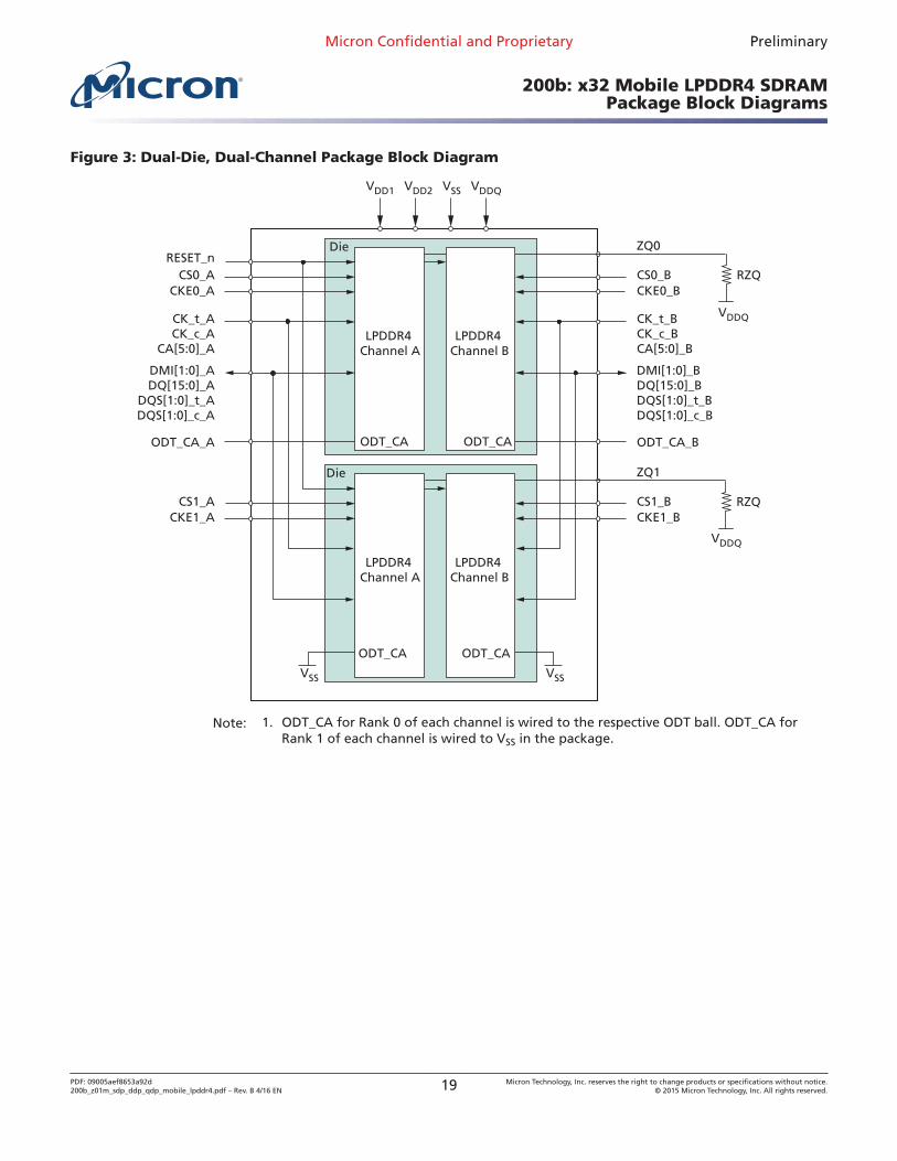
Figure 3: Dual-Die, Dual-Channel Package Block Diagram
Die
Die
LPDDR4 Channel A
VSSVSS
LPDDR4 Channel A
RESET_nCS0_A
CKE0_A
CK_t_ACK_c_A
CA[5:0]_A
DMI[1:0]_ADQ[15:0]_A
DQS[1:0]_t_ADQS[1:0]_c_A
ODT_CA_A
CS1_ACKE1_A
VDD1 VDD2 VSS VDDQ
ODT_CA
CKE0_BCS0_B
CK_t_BCK_c_BCA[5:0]_B
DMI[1:0]_BDQ[15:0]_BDQS[1:0]_t_BDQS[1:0]_c_B
ODT_CA_B
ZQ0
CKE1_BCS1_B
ZQ1
RZQ
VDDQ
RZQ
VDDQ
LPDDR4 Channel B
LPDDR4 Channel B
ODT_CA
ODT_CA ODT_CA
Note: 1. ODT_CA for Rank 0 of each channel is wired to the respective ODT ball. ODT_CA forRank 1 of each channel is wired to VSS in the package.
Micron Confidential and Proprietary Preliminary
200b: x32 Mobile LPDDR4 SDRAMPackage Block Diagrams
PDF: 09005aef8653a92d200b_z01m_sdp_ddp_qdp_mobile_lpddr4.pdf – Rev. B 4/16 EN 19 Micron Technology, Inc. reserves the right to change products or specifications without notice.
© 2015 Micron Technology, Inc. All rights reserved.
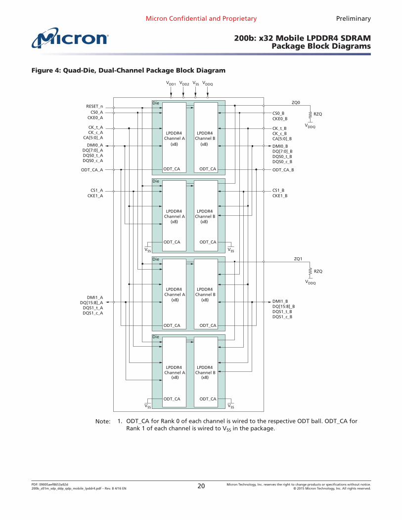
Figure 4: Quad-Die, Dual-Channel Package Block Diagram
CKE0_BCS0_B
CK_t_BCK_c_BCA[5:0]_B
DMI0_BDQ[7:0]_BDQS0_t_BDQS0_c_B
ODT_CA_B
RZQ
VDDQ
CKE1_BCS1_B
DMI1_BDQ[15:8]_BDQS1_t_BDQS1_c_B
ZQ1
ZQ0
RZQ
VDDQ
LPDDR4 Channel A
LPDDR4 Channel B
Die
(x8) (x8)
LPDDR4 Channel A
LPDDR4 Channel B
Die
LPDDR4 Channel A
LPDDR4 Channel B
Die
LPDDR4 Channel A
LPDDR4 Channel B
Die
RESET_nCS0_A
CKE0_A
CK_t_ACK_c_A
CA[5:0]_A
DMI0_ADQ[7:0]_ADQS0_t_ADQS0_c_A
ODT_CA_A
CS1_ACKE1_A
DMI1_ADQ[15:8]_A
DQS1_t_ADQS1_c_A
VDD1 VDD2 VSS VDDQ
VSS
VSS
VSS
VSS
ODT_CAODT_CA
ODT_CAODT_CA
ODT_CAODT_CA
ODT_CAODT_CA
(x8) (x8)
(x8) (x8)
(x8) (x8)
Note: 1. ODT_CA for Rank 0 of each channel is wired to the respective ODT ball. ODT_CA forRank 1 of each channel is wired to VSS in the package.
Micron Confidential and Proprietary Preliminary
200b: x32 Mobile LPDDR4 SDRAMPackage Block Diagrams
PDF: 09005aef8653a92d200b_z01m_sdp_ddp_qdp_mobile_lpddr4.pdf – Rev. B 4/16 EN 20 Micron Technology, Inc. reserves the right to change products or specifications without notice.
© 2015 Micron Technology, Inc. All rights reserved.
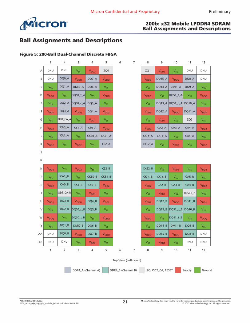
Ball Assignments and Descriptions
Figure 5: 200-Ball Dual-Channel Discrete FBGA
1
DNU
DNU
VSS
VDDQ
VSS
VDD1
VSS
VDD2
VSS
VDD2
VDD2
VSS
VDD2
VSS
VDD1
VSS
VDDQ
VSS
DNU
DNU
1
2
DNU
DQ0_A
DQ1_A
VSS
DQ2_A
DQ3_A
ODT_CA_A
CA0_A
CA1_A
VSS
VSS
CA1_B
CA0_B
ODT_CA_B
DQ3_B
DQ2_B
VSS
DQ1_B
DQ0_B
DNU
2
3
VSS
VDDQ
DMI0_A
DQS0_t_A
DQS0_c_A
VDDQ
VSS
CS1_A
VSS
VDD2
VDD2
VSS
CS1_B
VSS
VDDQ
DQS0_c_B
DQS0_t_B
DMI0_B
VDDQ
VSS
3
4
VDD2
DQ7_A
DQ6_A
VSS
DQ5_A
DQ4_A
VDD1
CS0_A
CKE0_A
VSS
VSS
CKE0_B
CS0_B
VDD1
DQ4_B
DQ5_B
VSS
DQ6_B
DQ7_B
VDD2
4
5
ZQ0
VDDQ
VSS
VDDQ
VSS
VDD2
VSS
VDD2
CKE1_A
CS2_A
CS2_B
CKE1_B
VDD2
VSS
VDD2
VSS
VDDQ
VSS
VDDQ
VSS
5
6
6
7
7
8
ZQ1
VDDQ
VSS
VDDQ
VSS
VDD2
VSS
VDD2
CK_t_A
CKE2_A
CKE2_B
CK_t_B
VDD2
VSS
VDD2
VSS
VDDQ
VSS
VDDQ
VSS
8
9
VDD2
DQ15_A
DQ14_A
VSS
DQ13_A
DQ12_A
VDD1
CA2_A
CK_c_A
VSS
VSS
CK_c_B
CA2_B
VDD1
DQ12_B
DQ13_B
VSS
DQ14_B
DQ15_B
VDD2
9
10
VSS
VDDQ
DMI1_A
DQS1_t_A
DQS1_c_A
VDDQ
VSS
CA3_A
VSS
VDD2
VDD2
VSS
CA3_B
VSS
VDDQ
DQS1_c_B
DQS1_t_B
DMI1_B
VDDQ
VSS
10
11
DNU
DQ8_A
DQ9_A
VSS
DQ10_A
DQ11_A
ZQ2
CA4_A
CA5_A
VSS
VSS
CA5_B
CA4_B
RESET_n
DQ11_B
DQ10_B
VSS
DQ9_B
DQ8_B
DNU
11
12
DNU
DNU
VSS
VDDQ
VSS
VDD1
VSS
VDD2
VSS
VDD2
VDD2
VSS
VDD2
VSS
VDD1
VSS
VDDQ
VSS
DNU
DNU
12
A
B
C
D
E
F
G
H
J
K
L
M
N
P
R
T
U
V
W
Y
AA
AB
Top View (ball down)
GroundSupplyZQ, ODT_CA, RESETDDR4_B (Channel B)DDR4_A (Channel A)
Micron Confidential and Proprietary Preliminary
200b: x32 Mobile LPDDR4 SDRAMBall Assignments and Descriptions
PDF: 09005aef8653a92d200b_z01m_sdp_ddp_qdp_mobile_lpddr4.pdf – Rev. B 4/16 EN 21 Micron Technology, Inc. reserves the right to change products or specifications without notice.
© 2015 Micron Technology, Inc. All rights reserved.
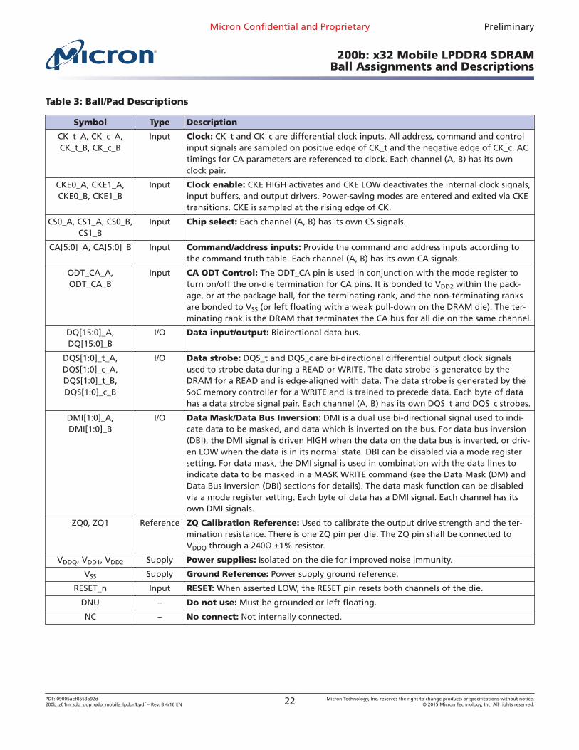
Table 3: Ball/Pad Descriptions
Symbol Type Description
CK_t_A, CK_c_A,CK_t_B, CK_c_B
Input Clock: CK_t and CK_c are differential clock inputs. All address, command and controlinput signals are sampled on positive edge of CK_t and the negative edge of CK_c. ACtimings for CA parameters are referenced to clock. Each channel (A, B) has its ownclock pair.
CKE0_A, CKE1_A,CKE0_B, CKE1_B
Input Clock enable: CKE HIGH activates and CKE LOW deactivates the internal clock signals,input buffers, and output drivers. Power-saving modes are entered and exited via CKEtransitions. CKE is sampled at the rising edge of CK.
CS0_A, CS1_A, CS0_B,CS1_B
Input Chip select: Each channel (A, B) has its own CS signals.
CA[5:0]_A, CA[5:0]_B Input Command/address inputs: Provide the command and address inputs according tothe command truth table. Each channel (A, B) has its own CA signals.
ODT_CA_A,ODT_CA_B
Input CA ODT Control: The ODT_CA pin is used in conjunction with the mode register toturn on/off the on-die termination for CA pins. It is bonded to VDD2 within the pack-age, or at the package ball, for the terminating rank, and the non-terminating ranksare bonded to VSS (or left floating with a weak pull-down on the DRAM die). The ter-minating rank is the DRAM that terminates the CA bus for all die on the same channel.
DQ[15:0]_A,DQ[15:0]_B
I/O Data input/output: Bidirectional data bus.
DQS[1:0]_t_A,DQS[1:0]_c_A,DQS[1:0]_t_B,DQS[1:0]_c_B
I/O Data strobe: DQS_t and DQS_c are bi-directional differential output clock signalsused to strobe data during a READ or WRITE. The data strobe is generated by theDRAM for a READ and is edge-aligned with data. The data strobe is generated by theSoC memory controller for a WRITE and is trained to precede data. Each byte of datahas a data strobe signal pair. Each channel (A, B) has its own DQS_t and DQS_c strobes.
DMI[1:0]_A,DMI[1:0]_B
I/O Data Mask/Data Bus Inversion: DMI is a dual use bi-directional signal used to indi-cate data to be masked, and data which is inverted on the bus. For data bus inversion(DBI), the DMI signal is driven HIGH when the data on the data bus is inverted, or driv-en LOW when the data is in its normal state. DBI can be disabled via a mode registersetting. For data mask, the DMI signal is used in combination with the data lines toindicate data to be masked in a MASK WRITE command (see the Data Mask (DM) andData Bus Inversion (DBI) sections for details). The data mask function can be disabledvia a mode register setting. Each byte of data has a DMI signal. Each channel has itsown DMI signals.
ZQ0, ZQ1 Reference ZQ Calibration Reference: Used to calibrate the output drive strength and the ter-mination resistance. There is one ZQ pin per die. The ZQ pin shall be connected toVDDQ through a 240Ω ±1% resistor.
VDDQ, VDD1, VDD2 Supply Power supplies: Isolated on the die for improved noise immunity.
VSS Supply Ground Reference: Power supply ground reference.
RESET_n Input RESET: When asserted LOW, the RESET pin resets both channels of the die.
DNU – Do not use: Must be grounded or left floating.
NC – No connect: Not internally connected.
Micron Confidential and Proprietary Preliminary
200b: x32 Mobile LPDDR4 SDRAMBall Assignments and Descriptions
PDF: 09005aef8653a92d200b_z01m_sdp_ddp_qdp_mobile_lpddr4.pdf – Rev. B 4/16 EN 22 Micron Technology, Inc. reserves the right to change products or specifications without notice.
© 2015 Micron Technology, Inc. All rights reserved.
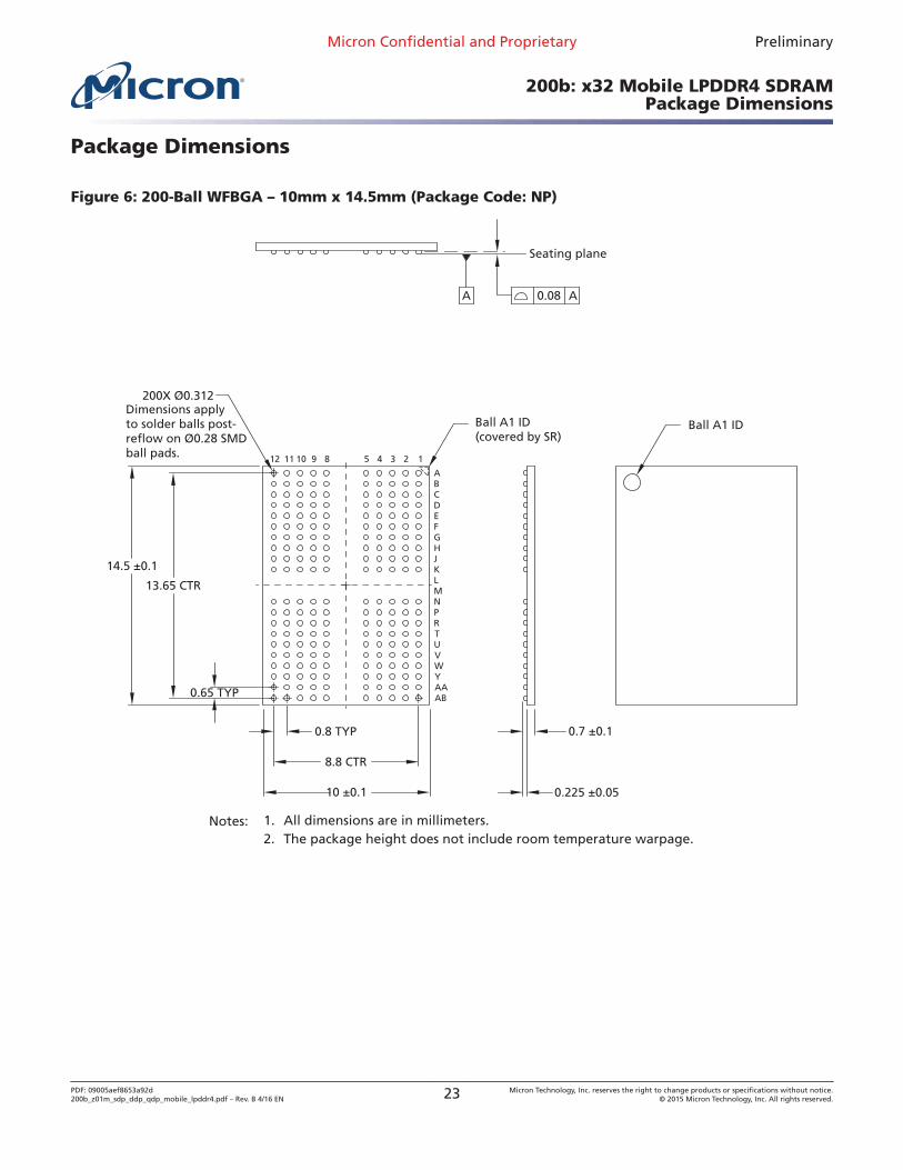
Package Dimensions
Figure 6: 200-Ball WFBGA – 10mm x 14.5mm (Package Code: NP)
Seating plane
0.08 A
Ball A1 ID(covered by SR)
Ball A1 ID
A
0.225 ±0.05
0.7 ±0.1
8.8 CTR
10 ±0.1
0.65 TYP
13.65 CTR
14.5 ±0.1
200X Ø0.312Dimensions applyto solder balls post-reflow on Ø0.28 SMDball pads.
0.8 TYP
ABCDEFGHJKLMNPRTUVWYAAAB
12 11 10 9 8 5 4 3 2 1
Notes: 1. All dimensions are in millimeters.2. The package height does not include room temperature warpage.
Micron Confidential and Proprietary Preliminary
200b: x32 Mobile LPDDR4 SDRAMPackage Dimensions
PDF: 09005aef8653a92d200b_z01m_sdp_ddp_qdp_mobile_lpddr4.pdf – Rev. B 4/16 EN 23 Micron Technology, Inc. reserves the right to change products or specifications without notice.
© 2015 Micron Technology, Inc. All rights reserved.
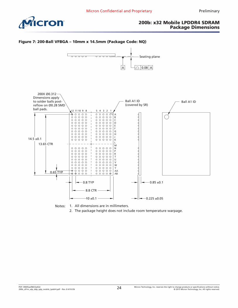
Figure 7: 200-Ball VFBGA – 10mm x 14.5mm (Package Code: NQ)
Seating plane
0.08 A
Ball A1 ID(covered by SR)
Ball A1 ID
A
0.225 ±0.05
0.85 ±0.1
8.8 CTR
10 ±0.1
0.65 TYP
13.65 CTR
14.5 ±0.1
200X Ø0.312Dimensions applyto solder balls post-reflow on Ø0.28 SMDball pads.
0.8 TYP
ABCDEFGHJKLMNPRTUVWYAAAB
12 11 10 9 8 5 4 3 2 1
Notes: 1. All dimensions are in millimeters.2. The package height does not include room temperature warpage.
Micron Confidential and Proprietary Preliminary
200b: x32 Mobile LPDDR4 SDRAMPackage Dimensions
PDF: 09005aef8653a92d200b_z01m_sdp_ddp_qdp_mobile_lpddr4.pdf – Rev. B 4/16 EN 24 Micron Technology, Inc. reserves the right to change products or specifications without notice.
© 2015 Micron Technology, Inc. All rights reserved.
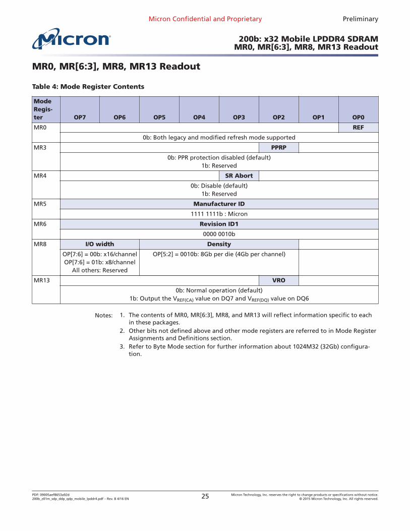
MR0, MR[6:3], MR8, MR13 Readout
Table 4: Mode Register Contents
ModeRegis-ter OP7 OP6 OP5 OP4 OP3 OP2 OP1 OP0
MR0 REF
0b: Both legacy and modified refresh mode supported
MR3 PPRP
0b: PPR protection disabled (default)1b: Reserved
MR4 SR Abort
0b: Disable (default)1b: Reserved
MR5 Manufacturer ID
1111 1111b : Micron
MR6 Revision ID1
0000 0010b
MR8 I/O width Density
OP[7:6] = 00b: x16/channelOP[7:6] = 01b: x8/channel
All others: Reserved
OP[5:2] = 0010b: 8Gb per die (4Gb per channel)
MR13 VRO
0b: Normal operation (default)1b: Output the VREF(CA) value on DQ7 and VREF(DQ) value on DQ6
Notes: 1. The contents of MR0, MR[6:3], MR8, and MR13 will reflect information specific to eachin these packages.
2. Other bits not defined above and other mode registers are referred to in Mode RegisterAssignments and Definitions section.
3. Refer to Byte Mode section for further information about 1024M32 (32Gb) configura-tion.
Micron Confidential and Proprietary Preliminary
200b: x32 Mobile LPDDR4 SDRAMMR0, MR[6:3], MR8, MR13 Readout
PDF: 09005aef8653a92d200b_z01m_sdp_ddp_qdp_mobile_lpddr4.pdf – Rev. B 4/16 EN 25 Micron Technology, Inc. reserves the right to change products or specifications without notice.
© 2015 Micron Technology, Inc. All rights reserved.
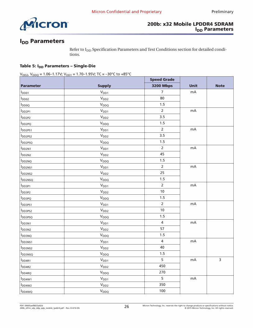
IDD ParametersRefer to IDD Specification Parameters and Test Conditions section for detailed condi-tions.
Table 5: IDD Parameters – Single-Die
VDD2, VDDQ = 1.06–1.17V; VDD1 = 1.70–1.95V; TC = –30°C to +85°C
Parameter Supply
Speed Grade
Unit Note3200 Mbps
IDD01 VDD1 7 mA
IDD02 VDD2 80
IDD0Q VDDQ 1.5
IDD2P1 VDD1 2 mA
IDD2P2 VDD2 3.5
IDD2PQ VDDQ 1.5
IDD2PS1 VDD1 2 mA
IDD2PS2 VDD2 3.5
IDD2PSQ VDDQ 1.5
IDD2N1 VDD1 2 mA
IDD2N2 VDD2 45
IDD2NQ VDDQ 1.5
IDD2NS1 VDD1 2 mA
IDD2NS2 VDD2 25
IDD2NSQ VDDQ 1.5
IDD3P1 VDD1 2 mA
IDD3P2 VDD2 10
IDD3PQ VDDQ 1.5
IDD3PS1 VDD1 2 mA
IDD3PS2 VDD2 10
IDD3PSQ VDDQ 1.5
IDD3N1 VDD1 4 mA
IDD3N2 VDD2 57
IDD3NQ VDDQ 1.5
IDD3NS1 VDD1 4 mA
IDD3NS2 VDD2 40
IDD3NSQ VDDQ 1.5
IDD4R1 VDD1 5 mA 3
IDD4R2 VDD2 450
IDD4RQ VDDQ 270
IDD4W1 VDD1 5 mA
IDD4W2 VDD2 350
IDD4WQ VDDQ 100
Micron Confidential and Proprietary Preliminary
200b: x32 Mobile LPDDR4 SDRAMIDD Parameters
PDF: 09005aef8653a92d200b_z01m_sdp_ddp_qdp_mobile_lpddr4.pdf – Rev. B 4/16 EN 26 Micron Technology, Inc. reserves the right to change products or specifications without notice.
© 2015 Micron Technology, Inc. All rights reserved.
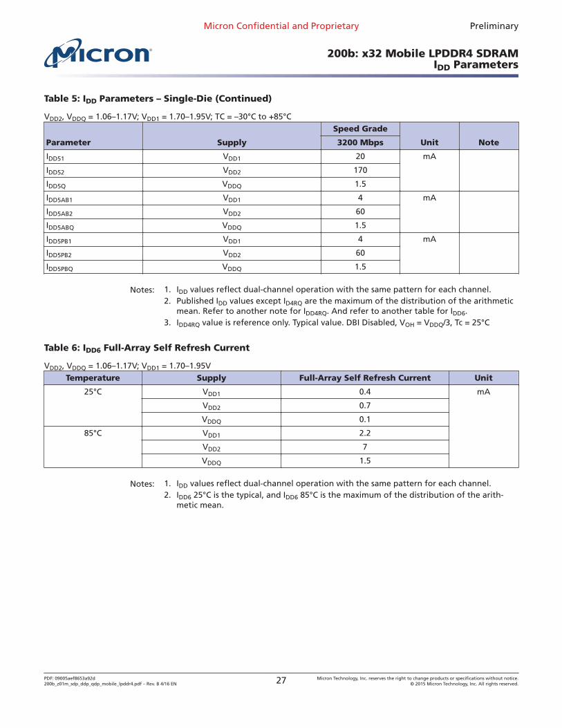
Table 5: IDD Parameters – Single-Die (Continued)
VDD2, VDDQ = 1.06–1.17V; VDD1 = 1.70–1.95V; TC = –30°C to +85°C
Parameter Supply
Speed Grade
Unit Note3200 Mbps
IDD51 VDD1 20 mA
IDD52 VDD2 170
IDD5Q VDDQ 1.5
IDD5AB1 VDD1 4 mA
IDD5AB2 VDD2 60
IDD5ABQ VDDQ 1.5
IDD5PB1 VDD1 4 mA
IDD5PB2 VDD2 60
IDD5PBQ VDDQ 1.5
Notes: 1. IDD values reflect dual-channel operation with the same pattern for each channel.2. Published IDD values except ID4RQ are the maximum of the distribution of the arithmetic
mean. Refer to another note for IDD4RQ. And refer to another table for IDD6.3. IDD4RQ value is reference only. Typical value. DBI Disabled, VOH = VDDQ/3, Tc = 25°C
Table 6: IDD6 Full-Array Self Refresh Current
VDD2, VDDQ = 1.06–1.17V; VDD1 = 1.70–1.95VTemperature Supply Full-Array Self Refresh Current Unit
25°C VDD1 0.4 mA
VDD2 0.7
VDDQ 0.1
85°C VDD1 2.2
VDD2 7
VDDQ 1.5
Notes: 1. IDD values reflect dual-channel operation with the same pattern for each channel.2. IDD6 25°C is the typical, and IDD6 85°C is the maximum of the distribution of the arith-
metic mean.
Micron Confidential and Proprietary Preliminary
200b: x32 Mobile LPDDR4 SDRAMIDD Parameters
PDF: 09005aef8653a92d200b_z01m_sdp_ddp_qdp_mobile_lpddr4.pdf – Rev. B 4/16 EN 27 Micron Technology, Inc. reserves the right to change products or specifications without notice.
© 2015 Micron Technology, Inc. All rights reserved.
Functional DescriptionThe Mobile Low-Power DDR4 SDRAM (LPDDR4) is a high-speed CMOS, dynamic ran-dom-access memory. The device is internally configured with 16 DQs and 8 banks perchannel.
LPDDR4 uses a 2-tick, single-data-rate (SDR) protocol on the CA bus to reduce thenumber of input signals in the system. The term "2-tick" means that the command/address is decoded across two transactions, such that half of the command/address iscaptured with each of two consecutive rising edges of CK. The 6-bit CA bus containscommand, address, and bank information. Some commands such as READ, WRITE,MASKED WRITE, and ACTIVATE require two consecutive 2-tick SDR commands tocomplete the instruction.
LPDDR4 uses a double-data-rate (DDR) protocol on the DQ bus to achieve high-speedoperation. The DDR interface transfers two data bits to each DQ lane in one clock cycleand is matched to a 16n-prefetch DRAM architecture. A write/read access consists of asingle 16n-bit-wide data transfer to/from the DRAM core and 16 corresponding n-bit-wide data transfers at the I/O pins.
Read and write accesses to the device are burst-oriented. Accesses start at a selectedcolumn address and continue for a programmed number of columns in a programmedsequence.
Accesses begin with the registration of an ACTIVATE command to open a row in thememory core, followed by a WRITE or READ command to access column data withinthe open row. The address and bank address (BA) bits registered by the ACTIVATE com-mand are used to select the bank and row to be opened. The address and BA bits regis-tered with the WRITE or READ command are used to select the bank and the startingcolumn address for the burst access.
Prior to normal operation, the LPDDR4 SDRAM must be initialized. Following sectionsprovide detailed information about device initialization, register definition, commanddescriptions and device operations.
Monolithic Device AddressingThe table below includes all monolithic device addressing options defined by JEDEC.Under the SDRAM Addressing heading near the beginning of this data sheet are ad-dressing details for this product data sheet.
Micron Confidential and Proprietary Preliminary
200b: x32 Mobile LPDDR4 SDRAMFunctional Description
PDF: 09005aef8653a92d200b_z01m_sdp_ddp_qdp_mobile_lpddr4.pdf – Rev. B 4/16 EN 28 Micron Technology, Inc. reserves the right to change products or specifications without notice.
© 2015 Micron Technology, Inc. All rights reserved.
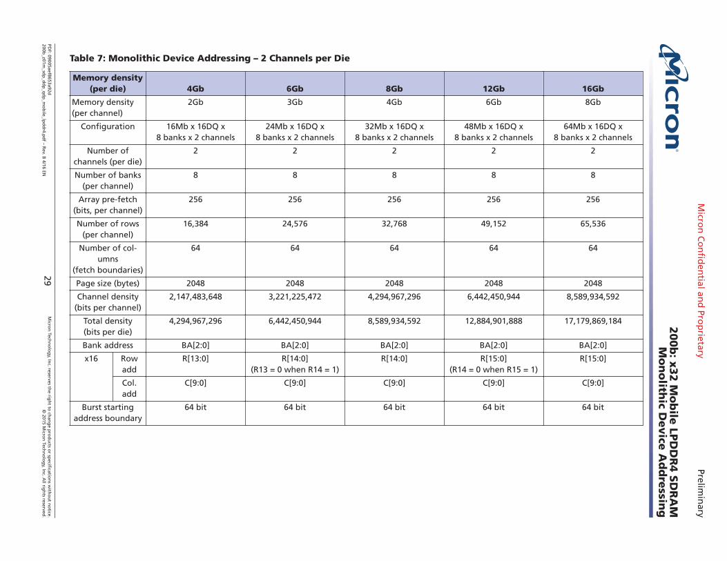
Table 7: Monolithic Device Addressing – 2 Channels per Die
Memory density(per die) 4Gb 6Gb 8Gb 12Gb 16Gb
Memory density(per channel)
2Gb 3Gb 4Gb 6Gb 8Gb
Configuration 16Mb x 16DQ x8 banks x 2 channels
24Mb x 16DQ x8 banks x 2 channels
32Mb x 16DQ x8 banks x 2 channels
48Mb x 16DQ x8 banks x 2 channels
64Mb x 16DQ x8 banks x 2 channels
Number ofchannels (per die)
2 2 2 2 2
Number of banks(per channel)
8 8 8 8 8
Array pre-fetch(bits, per channel)
256 256 256 256 256
Number of rows(per channel)
16,384 24,576 32,768 49,152 65,536
Number of col-umns
(fetch boundaries)
64 64 64 64 64
Page size (bytes) 2048 2048 2048 2048 2048
Channel density(bits per channel)
2,147,483,648 3,221,225,472 4,294,967,296 6,442,450,944 8,589,934,592
Total density(bits per die)
4,294,967,296 6,442,450,944 8,589,934,592 12,884,901,888 17,179,869,184
Bank address BA[2:0] BA[2:0] BA[2:0] BA[2:0] BA[2:0]
x16 Rowadd
R[13:0] R[14:0](R13 = 0 when R14 = 1)
R[14:0] R[15:0](R14 = 0 when R15 = 1)
R[15:0]
Col.add
C[9:0] C[9:0] C[9:0] C[9:0] C[9:0]
Burst startingaddress boundary
64 bit 64 bit 64 bit 64 bit 64 bit
Micro
n C
on
fiden
tial and
Prop
rietaryPrelim
inary
200b
: x32 M
ob
ile LP
DD
R4 S
DR
AM
Mo
no
lithic D
evice
Ad
dre
ssing
PDF: 09005aef8653a92d
200b_z01m
_sdp
_dd
p_q
dp
_mo
bile_lp
dd
r4.pd
f – Rev. B
4/16 EN29
Micro
n Tech
no
log
y, Inc. reserves th
e righ
t to ch
ang
e pro
du
cts or sp
ecification
s with
ou
t no
tice.©
2015 Micro
n Tech
no
log
y, Inc. A
ll righ
ts reserved.
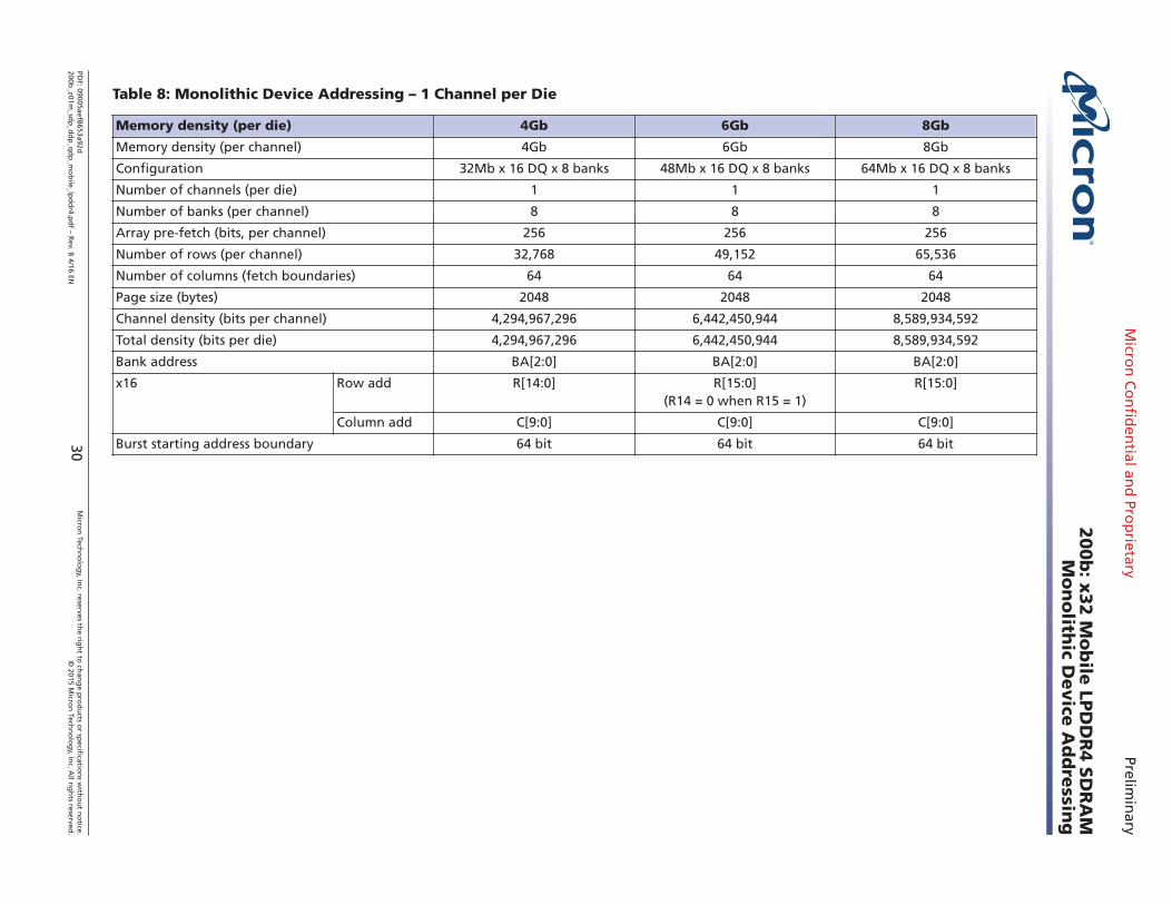
Table 8: Monolithic Device Addressing – 1 Channel per Die
Memory density (per die) 4Gb 6Gb 8Gb
Memory density (per channel) 4Gb 6Gb 8Gb
Configuration 32Mb x 16 DQ x 8 banks 48Mb x 16 DQ x 8 banks 64Mb x 16 DQ x 8 banks
Number of channels (per die) 1 1 1
Number of banks (per channel) 8 8 8
Array pre-fetch (bits, per channel) 256 256 256
Number of rows (per channel) 32,768 49,152 65,536
Number of columns (fetch boundaries) 64 64 64
Page size (bytes) 2048 2048 2048
Channel density (bits per channel) 4,294,967,296 6,442,450,944 8,589,934,592
Total density (bits per die) 4,294,967,296 6,442,450,944 8,589,934,592
Bank address BA[2:0] BA[2:0] BA[2:0]
x16 Row add R[14:0] R[15:0](R14 = 0 when R15 = 1)
R[15:0]
Column add C[9:0] C[9:0] C[9:0]
Burst starting address boundary 64 bit 64 bit 64 bit
Micro
n C
on
fiden
tial and
Prop
rietaryPrelim
inary
200b
: x32 M
ob
ile LP
DD
R4 S
DR
AM
Mo
no
lithic D
evice
Ad
dre
ssing
PDF: 09005aef8653a92d
200b_z01m
_sdp
_dd
p_q
dp
_mo
bile_lp
dd
r4.pd
f – Rev. B
4/16 EN30
Micro
n Tech
no
log
y, Inc. reserves th
e righ
t to ch
ang
e pro
du
cts or sp
ecification
s with
ou
t no
tice.©
2015 Micro
n Tech
no
log
y, Inc. A
ll righ
ts reserved.
Notes: 1. The lower two column addresses (C0–C1) are assumed to be zero and are not transmit-ted on the CA bus.
2. Row and column address values on the CA bus that are not used for a particular densityshould be at valid logic levels.
3. For non - binary memory densities, only a half of the row address space is valid. Whenthe MSB address bit is HIGH, then the MSB - 1 address bit must be LOW.
Micron Confidential and Proprietary Preliminary
200b: x32 Mobile LPDDR4 SDRAMMonolithic Device Addressing
PDF: 09005aef8653a92d200b_z01m_sdp_ddp_qdp_mobile_lpddr4.pdf – Rev. B 4/16 EN 31 Micron Technology, Inc. reserves the right to change products or specifications without notice.
© 2015 Micron Technology, Inc. All rights reserved.
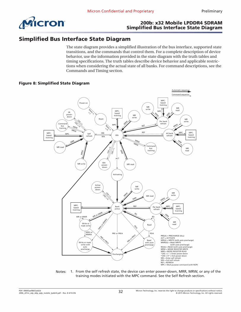
Simplified Bus Interface State DiagramThe state diagram provides a simplified illustration of the bus interface, supported statetransitions, and the commands that control them. For a complete description of devicebehavior, use the information provided in the state diagram with the truth tables andtiming specifications. The truth tables describe device behavior and applicable restric-tions when considering the actual state of all banks. For command descriptions, see theCommands and Timing section.
Figure 8: Simplified State Diagram
MRW
MRW
Automatic sequence
Command sequence
Reset
All bankrefresh
Power-on
Selfrefresh
MR write
Idle
Activating
Bankactive
Precharging
Write ormask write Read
Readwith autoprecharge
Write or maskwrite with
autoprecharge
MR read
MPC
MRWMRW
CKE = L
CKE = H
CKE
= L
CKE
= H
Reset_n= H
Reset_n= L
SRE
SRX
MRW
MR readIdle
power-down
WR or MWR RD
MRR
MRR
REF
Per bankrefresh
REF
MRWMRW
MPC
WRA orMWRA
WRA
or M
WRA
RDA
RDA
RDWR or MWR
PRE(A) = PRECHARGE (ALL)ACT = ACTIVATEWR(A) = WRITE (with auto precharge)MWR(A) = Mask WRITE (with auto precharge)RD(A) = READ (with auto precharge)MRW = MODE REGISTER WRITEMRR = MODE REGISTER READ"CKE = L" = Enter power-down"CKE = H" = Exit power-downSRE = Enter self refreshSRX = Exit self refreshREF = REFRESHMPC = Mult-purpose command (with NOP)
PRE or PREA
PRE or PREA PRE o
r PREA
ACT
MPC
MRwrite
MRwrite
MRR
MRread
REF
Per bankrefresh
MRRMR read
Commandbus
training
Commandbus
training
MPC-based
training
MPC
MPC-based
training
MPC-based
training
MPC-based
training
MPC-based
training
SRpower-down
CKE = L
CKE = H
Activepower-down
MRW
MRwrite
MRR
MRread
MRW
MRwrite
MPC MPC-based
training
MRR
MRread
MRW
MRwrite
Notes: 1. From the self refresh state, the device can enter power-down, MRR, MRW, or any of thetraining modes initiated with the MPC command. See the Self Refresh section.
Micron Confidential and Proprietary Preliminary
200b: x32 Mobile LPDDR4 SDRAMSimplified Bus Interface State Diagram
PDF: 09005aef8653a92d200b_z01m_sdp_ddp_qdp_mobile_lpddr4.pdf – Rev. B 4/16 EN 32 Micron Technology, Inc. reserves the right to change products or specifications without notice.
© 2015 Micron Technology, Inc. All rights reserved.
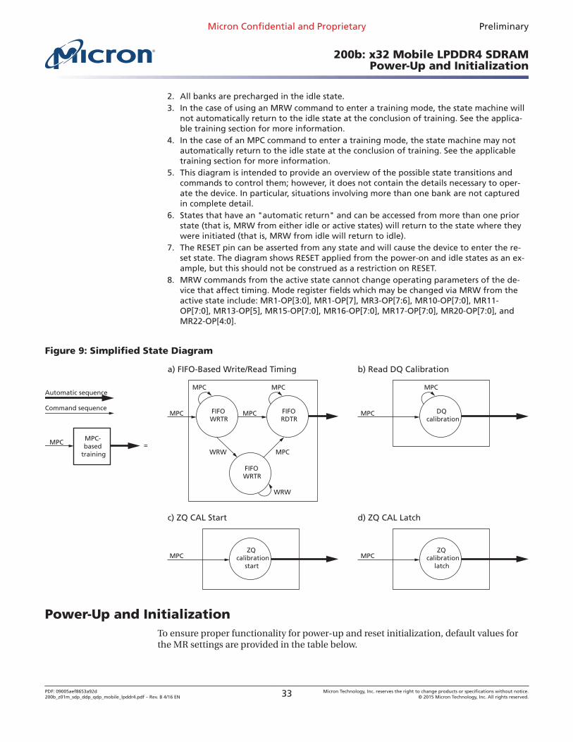
2. All banks are precharged in the idle state.3. In the case of using an MRW command to enter a training mode, the state machine will
not automatically return to the idle state at the conclusion of training. See the applica-ble training section for more information.
4. In the case of an MPC command to enter a training mode, the state machine may notautomatically return to the idle state at the conclusion of training. See the applicabletraining section for more information.
5. This diagram is intended to provide an overview of the possible state transitions andcommands to control them; however, it does not contain the details necessary to oper-ate the device. In particular, situations involving more than one bank are not capturedin complete detail.
6. States that have an "automatic return" and can be accessed from more than one priorstate (that is, MRW from either idle or active states) will return to the state where theywere initiated (that is, MRW from idle will return to idle).
7. The RESET pin can be asserted from any state and will cause the device to enter the re-set state. The diagram shows RESET applied from the power-on and idle states as an ex-ample, but this should not be construed as a restriction on RESET.
8. MRW commands from the active state cannot change operating parameters of the de-vice that affect timing. Mode register fields which may be changed via MRW from theactive state include: MR1-OP[3:0], MR1-OP[7], MR3-OP[7:6], MR10-OP[7:0], MR11-OP[7:0], MR13-OP[5], MR15-OP[7:0], MR16-OP[7:0], MR17-OP[7:0], MR20-OP[7:0], andMR22-OP[4:0].
Figure 9: Simplified State Diagram
Automatic sequence
Command sequence
MPC =
MPC MPC
MPC MPC
FIFOWRTR
FIFOWRTR
WRW
WRW
MPC
a) FIFO-Based Write/Read Timing
MPC FIFORDTR
MPCMPC
MPC-based
training
b) Read DQ Calibration
DQcalibration
MPC
c) ZQ CAL Start
ZQcalibration
start
d) ZQ CAL Latch
ZQcalibration
latch
Power-Up and InitializationTo ensure proper functionality for power-up and reset initialization, default values forthe MR settings are provided in the table below.
Micron Confidential and Proprietary Preliminary
200b: x32 Mobile LPDDR4 SDRAMPower-Up and Initialization
PDF: 09005aef8653a92d200b_z01m_sdp_ddp_qdp_mobile_lpddr4.pdf – Rev. B 4/16 EN 33 Micron Technology, Inc. reserves the right to change products or specifications without notice.
© 2015 Micron Technology, Inc. All rights reserved.
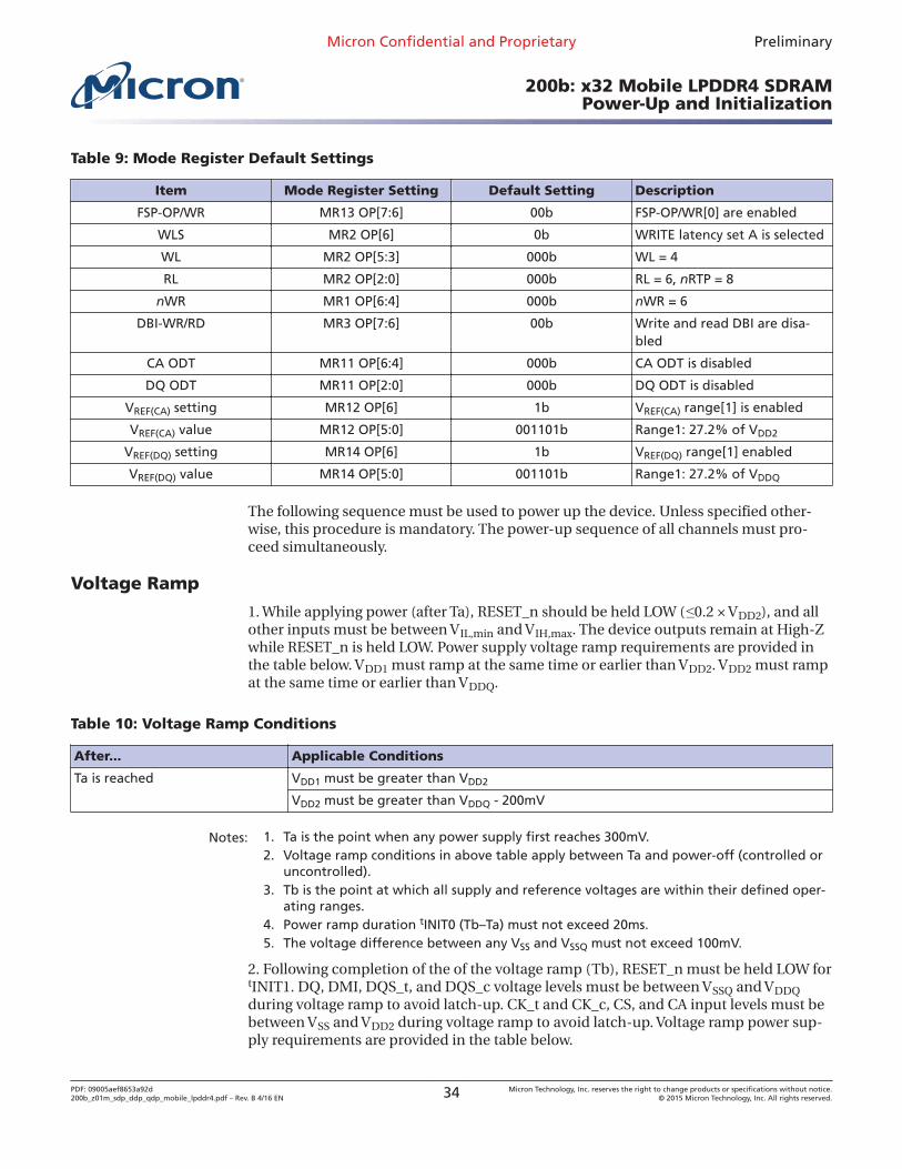
Table 9: Mode Register Default Settings
Item Mode Register Setting Default Setting Description
FSP-OP/WR MR13 OP[7:6] 00b FSP-OP/WR[0] are enabled
WLS MR2 OP[6] 0b WRITE latency set A is selected
WL MR2 OP[5:3] 000b WL = 4
RL MR2 OP[2:0] 000b RL = 6, nRTP = 8
nWR MR1 OP[6:4] 000b nWR = 6
DBI-WR/RD MR3 OP[7:6] 00b Write and read DBI are disa-bled
CA ODT MR11 OP[6:4] 000b CA ODT is disabled
DQ ODT MR11 OP[2:0] 000b DQ ODT is disabled
VREF(CA) setting MR12 OP[6] 1b VREF(CA) range[1] is enabled
VREF(CA) value MR12 OP[5:0] 001101b Range1: 27.2% of VDD2
VREF(DQ) setting MR14 OP[6] 1b VREF(DQ) range[1] enabled
VREF(DQ) value MR14 OP[5:0] 001101b Range1: 27.2% of VDDQ
The following sequence must be used to power up the device. Unless specified other-wise, this procedure is mandatory. The power-up sequence of all channels must pro-ceed simultaneously.
Voltage Ramp
1. While applying power (after Ta), RESET_n should be held LOW (≤0.2 × VDD2), and allother inputs must be between VIL,min and VIH,max. The device outputs remain at High-Zwhile RESET_n is held LOW. Power supply voltage ramp requirements are provided inthe table below. VDD1 must ramp at the same time or earlier than VDD2. VDD2 must rampat the same time or earlier than VDDQ.
Table 10: Voltage Ramp Conditions
After... Applicable Conditions
Ta is reached VDD1 must be greater than VDD2
VDD2 must be greater than VDDQ - 200mV
Notes: 1. Ta is the point when any power supply first reaches 300mV.2. Voltage ramp conditions in above table apply between Ta and power-off (controlled or
uncontrolled).3. Tb is the point at which all supply and reference voltages are within their defined oper-
ating ranges.4. Power ramp duration tINIT0 (Tb–Ta) must not exceed 20ms.5. The voltage difference between any VSS and VSSQ must not exceed 100mV.
2. Following completion of the of the voltage ramp (Tb), RESET_n must be held LOW fortINIT1. DQ, DMI, DQS_t, and DQS_c voltage levels must be between VSSQ and VDDQduring voltage ramp to avoid latch-up. CK_t and CK_c, CS, and CA input levels must bebetween VSS and VDD2 during voltage ramp to avoid latch-up. Voltage ramp power sup-ply requirements are provided in the table below.
Micron Confidential and Proprietary Preliminary
200b: x32 Mobile LPDDR4 SDRAMPower-Up and Initialization
PDF: 09005aef8653a92d200b_z01m_sdp_ddp_qdp_mobile_lpddr4.pdf – Rev. B 4/16 EN 34 Micron Technology, Inc. reserves the right to change products or specifications without notice.
© 2015 Micron Technology, Inc. All rights reserved.
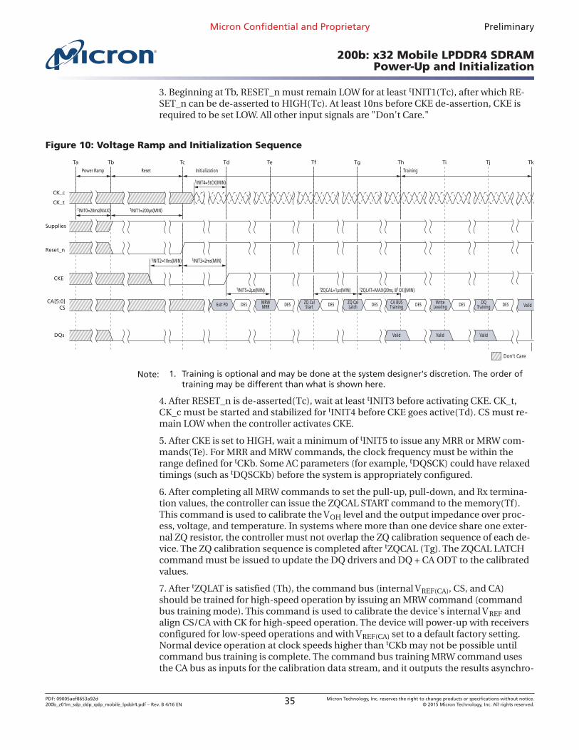
3. Beginning at Tb, RESET_n must remain LOW for at least tINIT1(Tc), after which RE-SET_n can be de-asserted to HIGH(Tc). At least 10ns before CKE de-assertion, CKE isrequired to be set LOW. All other input signals are "Don't Care."
Figure 10: Voltage Ramp and Initialization Sequence
Ta
CK_t
CK_c
Tb Tc Te Tf Tg Th Ti Tj Tk
Power Ramp Reset Initialization
tINIT0=20ms(MAX) tINIT1=200μs(MIN)
Td
DESDQTrainingDESWrite
LevelingDESCA BUSTrainingDESZQ Cal
LatchDESZQ CalStartDESMRW
MRRDESExit PD
tINIT4=5tCK(MIN)
Reset_n
Supplies
CKE
tINIT2=10ns(MIN) tINIT3=2ms(MIN)
tINIT5=2μs(MIN)
Training
tZQCAL=1μs(MIN) t
CA[5:0]CS
DQs
Don’t Care
ZQLAT=MAX(30ns, 8t CK)(MIN)
Valid
Valid ValidValid
Note: 1. Training is optional and may be done at the system designer's discretion. The order oftraining may be different than what is shown here.
4. After RESET_n is de-asserted(Tc), wait at least tINIT3 before activating CKE. CK_t,CK_c must be started and stabilized for tINIT4 before CKE goes active(Td). CS must re-main LOW when the controller activates CKE.
5. After CKE is set to HIGH, wait a minimum of tINIT5 to issue any MRR or MRW com-mands(Te). For MRR and MRW commands, the clock frequency must be within therange defined for tCKb. Some AC parameters (for example, tDQSCK) could have relaxedtimings (such as tDQSCKb) before the system is appropriately configured.
6. After completing all MRW commands to set the pull-up, pull-down, and Rx termina-tion values, the controller can issue the ZQCAL START command to the memory(Tf).This command is used to calibrate the VOH level and the output impedance over proc-ess, voltage, and temperature. In systems where more than one device share one exter-nal ZQ resistor, the controller must not overlap the ZQ calibration sequence of each de-vice. The ZQ calibration sequence is completed after tZQCAL (Tg). The ZQCAL LATCHcommand must be issued to update the DQ drivers and DQ + CA ODT to the calibratedvalues.
7. After tZQLAT is satisfied (Th), the command bus (internal VREF(CA), CS, and CA)should be trained for high-speed operation by issuing an MRW command (commandbus training mode). This command is used to calibrate the device's internal VREF andalign CS/CA with CK for high-speed operation. The device will power-up with receiversconfigured for low-speed operations and with VREF(CA) set to a default factory setting.Normal device operation at clock speeds higher than tCKb may not be possible untilcommand bus training is complete. The command bus training MRW command usesthe CA bus as inputs for the calibration data stream, and it outputs the results asynchro-
Micron Confidential and Proprietary Preliminary
200b: x32 Mobile LPDDR4 SDRAMPower-Up and Initialization
PDF: 09005aef8653a92d200b_z01m_sdp_ddp_qdp_mobile_lpddr4.pdf – Rev. B 4/16 EN 35 Micron Technology, Inc. reserves the right to change products or specifications without notice.
© 2015 Micron Technology, Inc. All rights reserved.
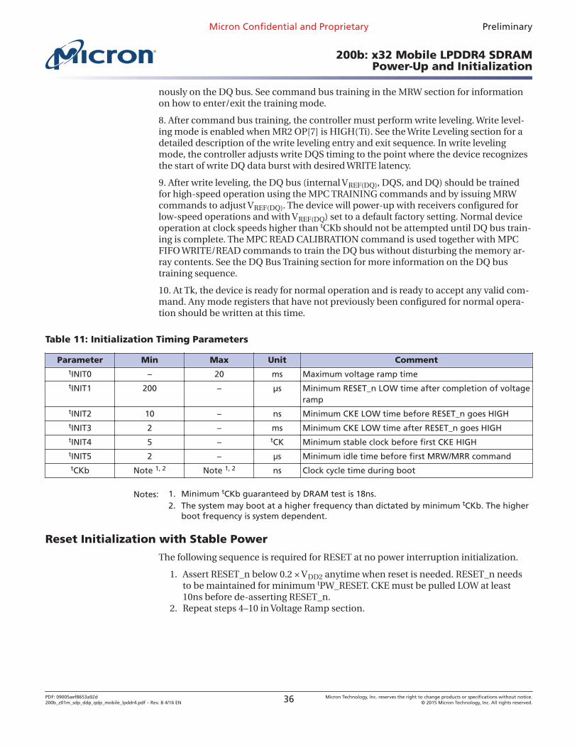
nously on the DQ bus. See command bus training in the MRW section for informationon how to enter/exit the training mode.
8. After command bus training, the controller must perform write leveling. Write level-ing mode is enabled when MR2 OP[7] is HIGH(Ti). See the Write Leveling section for adetailed description of the write leveling entry and exit sequence. In write levelingmode, the controller adjusts write DQS timing to the point where the device recognizesthe start of write DQ data burst with desired WRITE latency.
9. After write leveling, the DQ bus (internal VREF(DQ), DQS, and DQ) should be trainedfor high-speed operation using the MPC TRAINING commands and by issuing MRWcommands to adjust VREF(DQ). The device will power-up with receivers configured forlow-speed operations and with VREF(DQ) set to a default factory setting. Normal deviceoperation at clock speeds higher than tCKb should not be attempted until DQ bus train-ing is complete. The MPC READ CALIBRATION command is used together with MPCFIFO WRITE/READ commands to train the DQ bus without disturbing the memory ar-ray contents. See the DQ Bus Training section for more information on the DQ bustraining sequence.
10. At Tk, the device is ready for normal operation and is ready to accept any valid com-mand. Any mode registers that have not previously been configured for normal opera-tion should be written at this time.
Table 11: Initialization Timing Parameters
Parameter Min Max Unit CommenttINIT0 – 20 ms Maximum voltage ramp timetINIT1 200 – μs Minimum RESET_n LOW time after completion of voltage
ramptINIT2 10 – ns Minimum CKE LOW time before RESET_n goes HIGHtINIT3 2 – ms Minimum CKE LOW time after RESET_n goes HIGHtINIT4 5 – tCK Minimum stable clock before first CKE HIGHtINIT5 2 – μs Minimum idle time before first MRW/MRR commandtCKb Note 1, 2 Note 1, 2 ns Clock cycle time during boot
Notes: 1. Minimum tCKb guaranteed by DRAM test is 18ns.2. The system may boot at a higher frequency than dictated by minimum tCKb. The higher
boot frequency is system dependent.
Reset Initialization with Stable Power
The following sequence is required for RESET at no power interruption initialization.
1. Assert RESET_n below 0.2 × VDD2 anytime when reset is needed. RESET_n needsto be maintained for minimum tPW_RESET. CKE must be pulled LOW at least10ns before de-asserting RESET_n.
2. Repeat steps 4–10 in Voltage Ramp section.
Micron Confidential and Proprietary Preliminary
200b: x32 Mobile LPDDR4 SDRAMPower-Up and Initialization
PDF: 09005aef8653a92d200b_z01m_sdp_ddp_qdp_mobile_lpddr4.pdf – Rev. B 4/16 EN 36 Micron Technology, Inc. reserves the right to change products or specifications without notice.
© 2015 Micron Technology, Inc. All rights reserved.
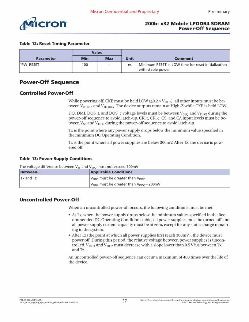
Table 12: Reset Timing Parameter
Parameter
Value
Unit CommentMin MaxtPW_RESET 100 – ns Minimum RESET_n LOW time for reset initialization
with stable power
Power-Off Sequence
Controlled Power-Off
While powering off, CKE must be held LOW (≤0.2 × VDD2); all other inputs must be be-tween VIL,min and VIH,max. The device outputs remain at High-Z while CKE is held LOW.
DQ, DMI, DQS_t, and DQS_c voltage levels must be between VSSQ and VDDQ during thepower-off sequence to avoid latch-up. CK_t, CK_c, CS, and CA input levels must be be-tween VSS and VDD2 during the power-off sequence to avoid latch-up.
Tx is the point where any power supply drops below the minimum value specified inthe minimum DC Operating Condition.
Tz is the point where all power supplies are below 300mV. After Tz, the device is pow-ered off.
Table 13: Power Supply Conditions
The voltage difference between VSS and VSSQ must not exceed 100mVBetween... Applicable Conditions
Tx and Tz VDD1 must be greater than VDD2
VDD2 must be greater than VDDQ - 200mV
Uncontrolled Power-Off
When an uncontrolled power-off occurs, the following conditions must be met.
• At Tx, when the power supply drops below the minimum values specified in the Rec-ommended DC Operating Conditions table, all power supplies must be turned off andall power supply current capacity must be at zero, except for any static charge remain-ing in the system.
• After Tz (the point at which all power supplies first reach 300mV), the device mustpower off. During this period, the relative voltage between power supplies is uncon-trolled. VDD1 and VDD2 must decrease with a slope lower than 0.5 V/μs between Txand Tz.
An uncontrolled power-off sequence can occur a maximum of 400 times over the life ofthe device.
Micron Confidential and Proprietary Preliminary
200b: x32 Mobile LPDDR4 SDRAMPower-Off Sequence
PDF: 09005aef8653a92d200b_z01m_sdp_ddp_qdp_mobile_lpddr4.pdf – Rev. B 4/16 EN 37 Micron Technology, Inc. reserves the right to change products or specifications without notice.
© 2015 Micron Technology, Inc. All rights reserved.
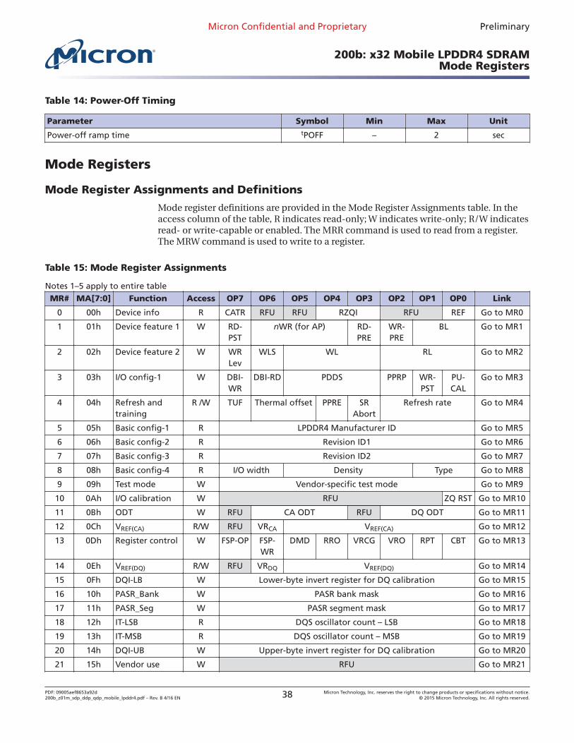
Table 14: Power-Off Timing
Parameter Symbol Min Max Unit
Power-off ramp time tPOFF – 2 sec
Mode Registers
Mode Register Assignments and Definitions
Mode register definitions are provided in the Mode Register Assignments table. In theaccess column of the table, R indicates read-only; W indicates write-only; R/W indicatesread- or write-capable or enabled. The MRR command is used to read from a register.The MRW command is used to write to a register.
Table 15: Mode Register Assignments
Notes 1–5 apply to entire tableMR# MA[7:0] Function Access OP7 OP6 OP5 OP4 OP3 OP2 OP1 OP0 Link
0 00h Device info R CATR RFU RFU RZQI RFU REF Go to MR0
1 01h Device feature 1 W RD-PST
nWR (for AP) RD-PRE
WR-PRE
BL Go to MR1
2 02h Device feature 2 W WRLev
WLS WL RL Go to MR2
3 03h I/O config-1 W DBI-WR
DBI-RD PDDS PPRP WR-PST
PU-CAL
Go to MR3
4 04h Refresh andtraining
R /W TUF Thermal offset PPRE SRAbort
Refresh rate Go to MR4
5 05h Basic config-1 R LPDDR4 Manufacturer ID Go to MR5
6 06h Basic config-2 R Revision ID1 Go to MR6
7 07h Basic config-3 R Revision ID2 Go to MR7
8 08h Basic config-4 R I/O width Density Type Go to MR8
9 09h Test mode W Vendor-specific test mode Go to MR9
10 0Ah I/O calibration W RFU ZQ RST Go to MR10
11 0Bh ODT W RFU CA ODT RFU DQ ODT Go to MR11
12 0Ch VREF(CA) R/W RFU VRCA VREF(CA) Go to MR12
13 0Dh Register control W FSP-OP FSP-WR
DMD RRO VRCG VRO RPT CBT Go to MR13
14 0Eh VREF(DQ) R/W RFU VRDQ VREF(DQ) Go to MR14
15 0Fh DQI-LB W Lower-byte invert register for DQ calibration Go to MR15
16 10h PASR_Bank W PASR bank mask Go to MR16
17 11h PASR_Seg W PASR segment mask Go to MR17
18 12h IT-LSB R DQS oscillator count – LSB Go to MR18
19 13h IT-MSB R DQS oscillator count – MSB Go to MR19
20 14h DQI-UB W Upper-byte invert register for DQ calibration Go to MR20
21 15h Vendor use W RFU Go to MR21
Micron Confidential and Proprietary Preliminary
200b: x32 Mobile LPDDR4 SDRAMMode Registers
PDF: 09005aef8653a92d200b_z01m_sdp_ddp_qdp_mobile_lpddr4.pdf – Rev. B 4/16 EN 38 Micron Technology, Inc. reserves the right to change products or specifications without notice.
© 2015 Micron Technology, Inc. All rights reserved.
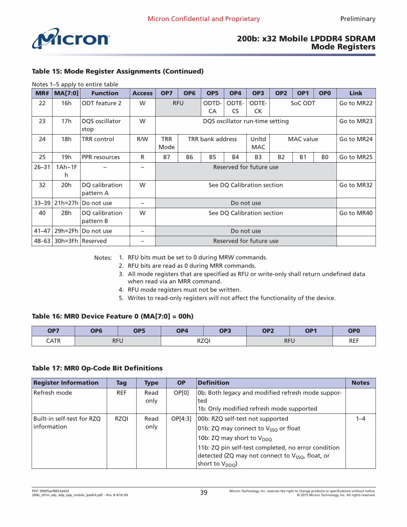
Table 15: Mode Register Assignments (Continued)
Notes 1–5 apply to entire tableMR# MA[7:0] Function Access OP7 OP6 OP5 OP4 OP3 OP2 OP1 OP0 Link
22 16h ODT feature 2 W RFU ODTD-CA
ODTE-CS
ODTE-CK
SoC ODT Go to MR22
23 17h DQS oscillatorstop
W DQS oscillator run-time setting Go to MR23
24 18h TRR control R/W TRRMode
TRR bank address UnltdMAC
MAC value Go to MR24
25 19h PPR resources R B7 B6 B5 B4 B3 B2 B1 B0 Go to MR25
26–31 1Ah~1Fh
– – Reserved for future use
32 20h DQ calibrationpattern A
W See DQ Calibration section Go to MR32
33–39 21h≈27h Do not use – Do not use
40 28h DQ calibrationpattern B
W See DQ Calibration section Go to MR40
41–47 29h≈2Fh Do not use – Do not use
48–63 30h≈3Fh Reserved – Reserved for future use
Notes: 1. RFU bits must be set to 0 during MRW commands.2. RFU bits are read as 0 during MRR commands.3. All mode registers that are specified as RFU or write-only shall return undefined data
when read via an MRR command.4. RFU mode registers must not be written.5. Writes to read-only registers will not affect the functionality of the device.
Table 16: MR0 Device Feature 0 (MA[7:0] = 00h)
OP7 OP6 OP5 OP4 OP3 OP2 OP1 OP0
CATR RFU RZQI RFU REF
Table 17: MR0 Op-Code Bit Definitions
Register Information Tag Type OP Definition Notes
Refresh mode REF Readonly
OP[0] 0b: Both legacy and modified refresh mode suppor-ted1b: Only modified refresh mode supported
Built-in self-test for RZQinformation
RZQI Readonly
OP[4:3] 00b: RZQ self-test not supported 1–4
01b: ZQ may connect to VSSQ or float
10b: ZQ may short to VDDQ
11b: ZQ pin self-test completed, no error conditiondetected (ZQ may not connect to VSSQ, float, orshort to VDDQ)
Micron Confidential and Proprietary Preliminary
200b: x32 Mobile LPDDR4 SDRAMMode Registers
PDF: 09005aef8653a92d200b_z01m_sdp_ddp_qdp_mobile_lpddr4.pdf – Rev. B 4/16 EN 39 Micron Technology, Inc. reserves the right to change products or specifications without notice.
© 2015 Micron Technology, Inc. All rights reserved.
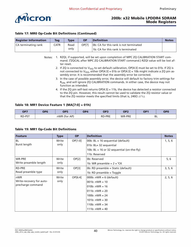
Table 17: MR0 Op-Code Bit Definitions (Continued)
Register Information Tag Type OP Definition Notes
CA terminating rank CATR Readonly
OP[7] 0b: CA for this rank is not terminated
1b: CA for this rank is terminated
Notes: 1. RZQI, if supported, will be set upon completion of MPC ZQ CALIBRATION START com-mand. (tZQCAL after MPC ZQ CALIBRATION START command.) RZQI value will be lost af-ter reset.
2. If ZQ is connected to VSSQ to set default calibration, OP[4:3] must be set to 01b. If ZQ isnot connected to VSSQ, either OP[4:3] = 01b or OP[4:3] = 10b might indicate a ZQ pin as-sembly error. It is recommended that the assembly error be corrected.
3. In the case of possible assembly error, the device will default to factory trim settings forRON, and will ignore ZQ CALIBRATION commands. In either case, the device may notfunction as intended.
4. If the ZQ pin self-test returns OP[4:3] = 11b, the device has detected a resistor connectedto the ZQ pin. However, this result cannot be used to validate the ZQ resistor value orthat the ZQ resistor meets the specified limits (that is, 240Ω
Table 18: MR1 Device Feature 1 (MA[7:0] = 01h)
OP7 OP6 OP5 OP4 OP3 OP2 OP1 OP0
RD-PST nWR (for AP) RD-PRE WR-PRE BL
Table 19: MR1 Op-Code Bit Definitions
Feature Type OP Definition Notes
BLBurst length
Writeonly
OP[1:0] 00b: BL = 16 sequential (default) 1, 5, 6
01b: BL= 32 sequential
10b: BL = 16 or 32 sequential (on-the-fly)
11b: Reserved
WR-PREWrite preamble length
Writeonly
OP[2] 0b: Reserved 5, 6
1b: WR preamble = 2 × tCK
RD-PRERead preamble type
Writeonly
OP[3] 0b: RD preamble = Static (default) 3, 5, 6
1b: RD preamble = Toggle
nWRWrite-recovery for auto-precharge command
Writeonly
OP[6:4] 000b: nWR = 6 (default) 2, 5, 6
001b: nWR = 10
010b: nWR = 16
011b: nWR = 20
100b: nWR = 24
101b: nWR = 30
110b: nWR = 34
111b: nWR = 40
Micron Confidential and Proprietary Preliminary
200b: x32 Mobile LPDDR4 SDRAMMode Registers
PDF: 09005aef8653a92d200b_z01m_sdp_ddp_qdp_mobile_lpddr4.pdf – Rev. B 4/16 EN 40 Micron Technology, Inc. reserves the right to change products or specifications without notice.
© 2015 Micron Technology, Inc. All rights reserved.
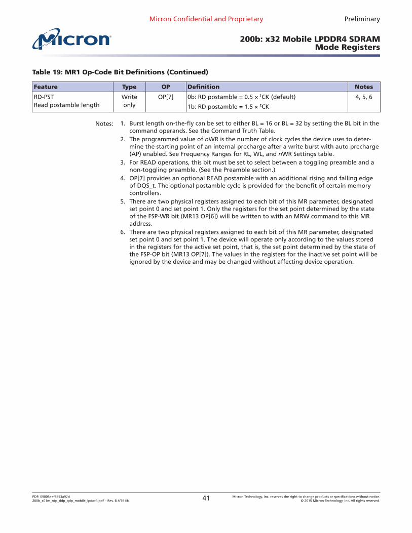
Table 19: MR1 Op-Code Bit Definitions (Continued)
Feature Type OP Definition Notes
RD-PSTRead postamble length
Writeonly
OP[7] 0b: RD postamble = 0.5 × tCK (default) 4, 5, 6
1b: RD postamble = 1.5 × tCK
Notes: 1. Burst length on-the-fly can be set to either BL = 16 or BL = 32 by setting the BL bit in thecommand operands. See the Command Truth Table.
2. The programmed value of nWR is the number of clock cycles the device uses to deter-mine the starting point of an internal precharge after a write burst with auto precharge(AP) enabled. See Frequency Ranges for RL, WL, and nWR Settings table.
3. For READ operations, this bit must be set to select between a toggling preamble and anon-toggling preamble. (See the Preamble section.)
4. OP[7] provides an optional READ postamble with an additional rising and falling edgeof DQS_t. The optional postamble cycle is provided for the benefit of certain memorycontrollers.
5. There are two physical registers assigned to each bit of this MR parameter, designatedset point 0 and set point 1. Only the registers for the set point determined by the stateof the FSP‐WR bit (MR13 OP[6]) will be written to with an MRW command to this MRaddress.
6. There are two physical registers assigned to each bit of this MR parameter, designatedset point 0 and set point 1. The device will operate only according to the values storedin the registers for the active set point, that is, the set point determined by the state ofthe FSP‐OP bit (MR13 OP[7]). The values in the registers for the inactive set point will beignored by the device and may be changed without affecting device operation.
Micron Confidential and Proprietary Preliminary
200b: x32 Mobile LPDDR4 SDRAMMode Registers
PDF: 09005aef8653a92d200b_z01m_sdp_ddp_qdp_mobile_lpddr4.pdf – Rev. B 4/16 EN 41 Micron Technology, Inc. reserves the right to change products or specifications without notice.
© 2015 Micron Technology, Inc. All rights reserved.
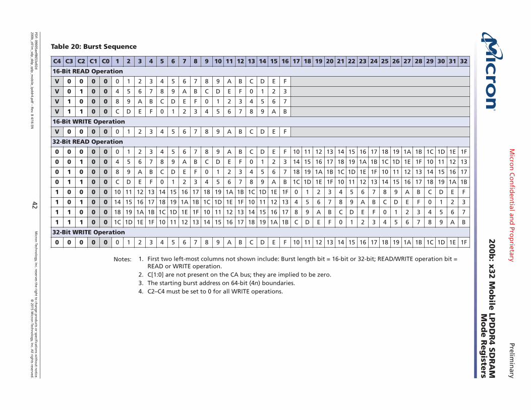
Table 20: Burst Sequence
C4 C3 C2 C1 C0 1 2 3 4 5 6 7 8 9 10 11 12 13 14 15 16 17 18 19 20 21 22 23 24 25 26 27 28 29 30 31 32
16-Bit READ Operation
V 0 0 0 0 0 1 2 3 4 5 6 7 8 9 A B C D E F
V 0 1 0 0 4 5 6 7 8 9 A B C D E F 0 1 2 3
V 1 0 0 0 8 9 A B C D E F 0 1 2 3 4 5 6 7
V 1 1 0 0 C D E F 0 1 2 3 4 5 6 7 8 9 A B
16-Bit WRITE Operation
V 0 0 0 0 0 1 2 3 4 5 6 7 8 9 A B C D E F
32-Bit READ Operation
0 0 0 0 0 0 1 2 3 4 5 6 7 8 9 A B C D E F 10 11 12 13 14 15 16 17 18 19 1A 1B 1C 1D 1E 1F
0 0 1 0 0 4 5 6 7 8 9 A B C D E F 0 1 2 3 14 15 16 17 18 19 1A 1B 1C 1D 1E 1F 10 11 12 13
0 1 0 0 0 8 9 A B C D E F 0 1 2 3 4 5 6 7 18 19 1A 1B 1C 1D 1E 1F 10 11 12 13 14 15 16 17
0 1 1 0 0 C D E F 0 1 2 3 4 5 6 7 8 9 A B 1C 1D 1E 1F 10 11 12 13 14 15 16 17 18 19 1A 1B
1 0 0 0 0 10 11 12 13 14 15 16 17 18 19 1A 1B 1C 1D 1E 1F 0 1 2 3 4 5 6 7 8 9 A B C D E F
1 0 1 0 0 14 15 16 17 18 19 1A 1B 1C 1D 1E 1F 10 11 12 13 4 5 6 7 8 9 A B C D E F 0 1 2 3
1 1 0 0 0 18 19 1A 1B 1C 1D 1E 1F 10 11 12 13 14 15 16 17 8 9 A B C D E F 0 1 2 3 4 5 6 7
1 1 1 0 0 1C 1D 1E 1F 10 11 12 13 14 15 16 17 18 19 1A 1B C D E F 0 1 2 3 4 5 6 7 8 9 A B
32-Bit WRITE Operation
0 0 0 0 0 0 1 2 3 4 5 6 7 8 9 A B C D E F 10 11 12 13 14 15 16 17 18 19 1A 1B 1C 1D 1E 1F
Notes: 1. First two left-most columns not shown include: Burst length bit = 16-bit or 32-bit; READ/WRITE operation bit =READ or WRITE operation.
2. C[1:0] are not present on the CA bus; they are implied to be zero.3. The starting burst address on 64-bit (4n) boundaries.4. C2–C4 must be set to 0 for all WRITE operations.
Micro
n C
on
fiden
tial and
Prop
rietaryPrelim
inary
200b
: x32 M
ob
ile LP
DD
R4 S
DR
AM
Mo
de R
eg
isters
PDF: 09005aef8653a92d
200b_z01m
_sdp
_dd
p_q
dp
_mo
bile_lp
dd
r4.pd
f – Rev. B
4/16 EN42
Micro
n Tech
no
log
y, Inc. reserves th
e righ
t to ch
ang
e pro
du
cts or sp
ecification
s with
ou
t no
tice.©
2015 Micro
n Tech
no
log
y, Inc. A
ll righ
ts reserved.
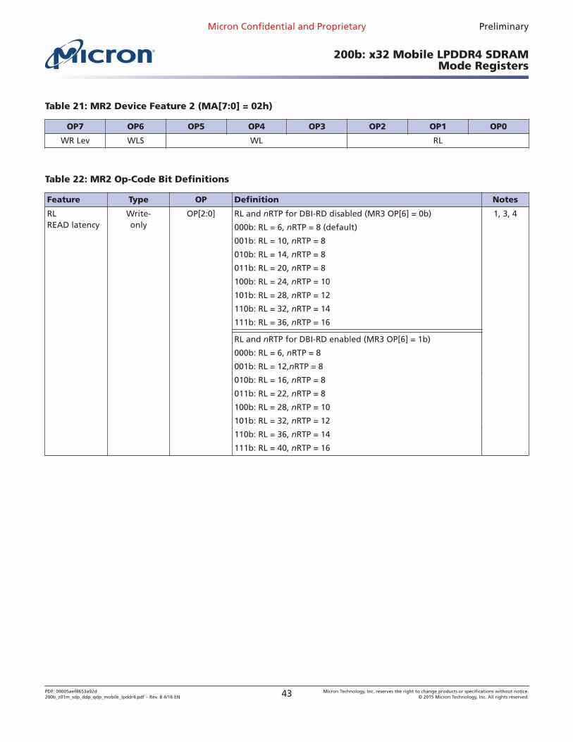
Table 21: MR2 Device Feature 2 (MA[7:0] = 02h)
OP7 OP6 OP5 OP4 OP3 OP2 OP1 OP0
WR Lev WLS WL RL
Table 22: MR2 Op-Code Bit Definitions
Feature Type OP Definition Notes
RLREAD latency
Write-only
OP[2:0] RL and nRTP for DBI-RD disabled (MR3 OP[6] = 0b) 1, 3, 4
000b: RL = 6, nRTP = 8 (default)
001b: RL = 10, nRTP = 8
010b: RL = 14, nRTP = 8
011b: RL = 20, nRTP = 8
100b: RL = 24, nRTP = 10
101b: RL = 28, nRTP = 12
110b: RL = 32, nRTP = 14
111b: RL = 36, nRTP = 16
RL and nRTP for DBI-RD enabled (MR3 OP[6] = 1b)
000b: RL = 6, nRTP = 8
001b: RL = 12,nRTP = 8
010b: RL = 16, nRTP = 8
011b: RL = 22, nRTP = 8
100b: RL = 28, nRTP = 10
101b: RL = 32, nRTP = 12
110b: RL = 36, nRTP = 14
111b: RL = 40, nRTP = 16
Micron Confidential and Proprietary Preliminary
200b: x32 Mobile LPDDR4 SDRAMMode Registers
PDF: 09005aef8653a92d200b_z01m_sdp_ddp_qdp_mobile_lpddr4.pdf – Rev. B 4/16 EN 43 Micron Technology, Inc. reserves the right to change products or specifications without notice.
© 2015 Micron Technology, Inc. All rights reserved.

Table 22: MR2 Op-Code Bit Definitions (Continued)
Feature Type OP Definition Notes
WLWRITE latency
Write-only
OP[5:3] WL Set A (MR2 OP[6] = 0b) 1, 3, 4
000b: WL = 4 (default)
001b: WL = 6
010b: WL = 8
011b: WL = 10
100b: WL = 12
101b: WL = 14
110b: WL = 16
111b: WL = 18
WL Set B (MR2 OP[6] = 1b)
000b: WL = 4
001b: WL = 8
010b: WL = 12
011b: WL = 18
100b: WL = 22
101b: WL = 26
110b: WL = 30
111b: WL = 34
WLSWRITE latencyset
Write-only
OP[6] 0b: Use WL Set A (default) 1, 3, 4
1b: Use WL Set B
WR LevWrite leveling
Write-only
OP[7] 0b: Disable write leveling (default) 2
1b: Enable write leveling
Notes: 1. See Latency Code Frequency Table for allowable frequency ranges for RL/WL/nWR.2. After an MRW command to set the write-leveling enable bit (OP[7] = 1b), the device re-
mains in the MRW state until another MRW command clears the bit (OP[7] = 0b). Noother commands are allowed until the write-leveling enable bit is cleared.
3. There are two physical registers assigned to each bit of this MR parameter, designatedset point 0 and set point 1. Only the registers for the set point determined by the stateof the FSP‐WR bit (MR13 OP[6]) will be written to with an MRW command this MR ad-dress, or read from with an MRR command to this address.
4. There are two physical registers assigned to each bit of this MR parameter, designatedset point 0 and set point 1. The device will operate only according to the values storedin the registers for the active set point, that is, the set point determined by the state ofthe FSP‐OP bit (MR13 OP[7]). The values in the registers for the inactive set point will beignored by the device and may be changed without affecting device operation.
5. nRTP is valid for BL16 only. For BL32, the SDRAM will add 8 clocks to the nRTP value be-fore starting a precharge.
Micron Confidential and Proprietary Preliminary
200b: x32 Mobile LPDDR4 SDRAMMode Registers
PDF: 09005aef8653a92d200b_z01m_sdp_ddp_qdp_mobile_lpddr4.pdf – Rev. B 4/16 EN 44 Micron Technology, Inc. reserves the right to change products or specifications without notice.
© 2015 Micron Technology, Inc. All rights reserved.
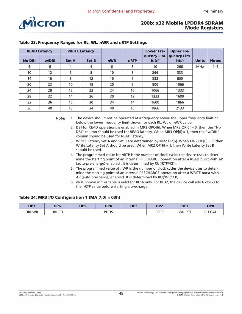
Table 23: Frequency Ranges for RL, WL, nWR and nRTP Settings
READ Latency WRITE Latency
nWR nRTP
Lower Fre-quency Lim-
it (>)
Upper Fre-quency Lim-
it(≤≤) Units NotesNo DBI w/DBI Set A Set B
6 6 4 4 6 8 10 266 MHz 1–6
10 12 6 8 10 8 266 533
14 16 8 12 16 8 533 800
20 22 10 18 20 8 800 1066
24 28 12 22 24 10 1066 1333
28 32 14 26 30 12 1333 1600
32 36 16 30 34 14 1600 1866
36 40 18 34 40 16 1866 2133
Notes: 1. The device should not be operated at a frequency above the upper frequency limit orbelow the lower frequency limit shown for each RL, WL or nWR value.
2. DBI for READ operations is enabled in MR3 OPO[6]. When MR3 OP[6] = 0, then the "NoDBI" column should be used for READ latency. When MR3 OP[6] = 1, then the "w/DBI"column should be used for READ latency.
3. WRITE Latency Set A and Set B are determined by MR2 OP[6]. When MR2 OP[6] = 0, thenWrite Latency Set A should be used. When MR2 OP[6] = 1, then Write Latency Set Bshould be used.
4. The programmed value for nRTP is the number of clock cycles the device uses to deter-mine the starting point of an internal PRECHARGE operation after a READ burst with AP(auto-pre-charge) enabled . It is determined by RU(tRTP/tCK).
5. The programmed value of nWR is the number of clock cycles the device uses to deter-mine the starting point of an internal PRECHARGE operation after a WRITE burst withAP (auto precharge) enabled. It is determined by RU(tWR/tCK).
6. nRTP shown in this table is valid for BL16 only. For BL32, the device will add 8 clocks tothe nRTP value before starting a precharge.
Table 24: MR3 I/O Configuration 1 (MA[7:0] = 03h)
OP7 OP6 OP5 OP4 OP3 OP2 OP1 OP0
DBI-WR DBI-RD PDDS PPRP WR-PST PU-CAL
Micron Confidential and Proprietary Preliminary
200b: x32 Mobile LPDDR4 SDRAMMode Registers
PDF: 09005aef8653a92d200b_z01m_sdp_ddp_qdp_mobile_lpddr4.pdf – Rev. B 4/16 EN 45 Micron Technology, Inc. reserves the right to change products or specifications without notice.
© 2015 Micron Technology, Inc. All rights reserved.
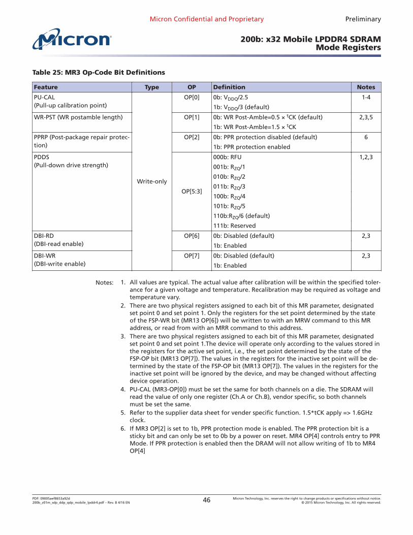
Table 25: MR3 Op-Code Bit Definitions
Feature Type OP Definition Notes
PU-CAL(Pull-up calibration point)
Write-only
OP[0] 0b: VDDQ/2.5 1-4
1b: VDDQ/3 (default)
WR-PST (WR postamble length) OP[1] 0b: WR Post-Amble=0.5 × tCK (default) 2,3,5
1b: WR Post-Amble=1.5 × tCK
PPRP (Post-package repair protec-tion)
OP[2] 0b: PPR protection disabled (default) 6
1b: PPR protection enabled
PDDS(Pull-down drive strength)
OP[5:3]
000b: RFU 1,2,3
001b: RZQ/1
010b: RZQ/2
011b: RZQ/3
100b: RZQ/4
101b: RZQ/5
110b:RZQ/6 (default)
111b: Reserved
DBI-RD(DBI-read enable)
OP[6] 0b: Disabled (default) 2,3
1b: Enabled
DBI-WR(DBI-write enable)
OP[7] 0b: Disabled (default) 2,3
1b: Enabled
Notes: 1. All values are typical. The actual value after calibration will be within the specified toler-ance for a given voltage and temperature. Recalibration may be required as voltage andtemperature vary.
2. There are two physical registers assigned to each bit of this MR parameter, designatedset point 0 and set point 1. Only the registers for the set point determined by the stateof the FSP‐WR bit (MR13 OP[6]) will be written to with an MRW command to this MRaddress, or read from with an MRR command to this address.
3. There are two physical registers assigned to each bit of this MR parameter, designatedset point 0 and set point 1.The device will operate only according to the values stored inthe registers for the active set point, i.e., the set point determined by the state of theFSP‐OP bit (MR13 OP[7]). The values in the registers for the inactive set point will be de-termined by the state of the FSP‐OP bit (MR13 OP[7]). The values in the registers for theinactive set point will be ignored by the device, and may be changed without affectingdevice operation.
4. PU‐CAL (MR3‐OP[0]) must be set the same for both channels on a die. The SDRAM willread the value of only one register (Ch.A or Ch.B), vendor specific, so both channelsmust be set the same.
5. Refer to the supplier data sheet for vender specific function. 1.5*tCK apply => 1.6GHzclock.
6. If MR3 OP[2] is set to 1b, PPR protection mode is enabled. The PPR protection bit is asticky bit and can only be set to 0b by a power on reset. MR4 OP[4] controls entry to PPRMode. If PPR protection is enabled then the DRAM will not allow writing of 1b to MR4OP[4]
Micron Confidential and Proprietary Preliminary
200b: x32 Mobile LPDDR4 SDRAMMode Registers
PDF: 09005aef8653a92d200b_z01m_sdp_ddp_qdp_mobile_lpddr4.pdf – Rev. B 4/16 EN 46 Micron Technology, Inc. reserves the right to change products or specifications without notice.
© 2015 Micron Technology, Inc. All rights reserved.
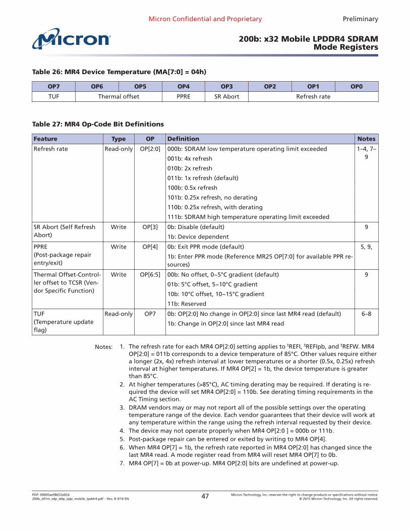
Table 26: MR4 Device Temperature (MA[7:0] = 04h)
OP7 OP6 OP5 OP4 OP3 OP2 OP1 OP0
TUF Thermal offset PPRE SR Abort Refresh rate
Table 27: MR4 Op-Code Bit Definitions
Feature Type OP Definition Notes
Refresh rate Read-only OP[2:0] 000b: SDRAM low temperature operating limit exceeded 1–4, 7–9001b: 4x refresh
010b: 2x refresh
011b: 1x refresh (default)
100b: 0.5x refresh
101b: 0.25x refresh, no derating
110b: 0.25x refresh, with derating
111b: SDRAM high temperature operating limit exceeded
SR Abort (Self RefreshAbort)
Write OP[3] 0b: Disable (default) 9
1b: Device dependent
PPRE(Post-package repairentry/exit)
Write OP[4] 0b: Exit PPR mode (default) 5, 9,
1b: Enter PPR mode (Reference MR25 OP[7:0] for available PPR re-sources)
Thermal Offset-Control-ler offset to TCSR (Ven-dor Specific Function)
Write OP[6:5] 00b: No offset, 0~5°C gradient (default) 9
01b: 5°C offset, 5~10°C gradient
10b: 10°C offset, 10~15°C gradient
11b: Reserved
TUF(Temperature updateflag)
Read-only OP7 0b: OP[2:0] No change in OP[2:0] since last MR4 read (default) 6–8
1b: Change in OP[2:0] since last MR4 read
Notes: 1. The refresh rate for each MR4 OP[2:0] setting applies to tREFI, tREFIpb, and tREFW. MR4OP[2:0] = 011b corresponds to a device temperature of 85°C. Other values require eithera longer (2x, 4x) refresh interval at lower temperatures or a shorter (0.5x, 0.25x) refreshinterval at higher temperatures. If MR4 OP[2] = 1b, the device temperature is greaterthan 85°C.
2. At higher temperatures (>85°C), AC timing derating may be required. If derating is re-quired the device will set MR4 OP[2:0] = 110b. See derating timing requirements in theAC Timing section.
3. DRAM vendors may or may not report all of the possible settings over the operatingtemperature range of the device. Each vendor guarantees that their device will work atany temperature within the range using the refresh interval requested by their device.
4. The device may not operate properly when MR4 OP[2:0 ] = 000b or 111b.5. Post‐package repair can be entered or exited by writing to MR4 OP[4].6. When MR4 OP[7] = 1b, the refresh rate reported in MR4 OP[2:0] has changed since the
last MR4 read. A mode register read from MR4 will reset MR4 OP[7] to 0b.7. MR4 OP[7] = 0b at power‐up. MR4 OP[2:0] bits are undefined at power‐up.
Micron Confidential and Proprietary Preliminary
200b: x32 Mobile LPDDR4 SDRAMMode Registers
PDF: 09005aef8653a92d200b_z01m_sdp_ddp_qdp_mobile_lpddr4.pdf – Rev. B 4/16 EN 47 Micron Technology, Inc. reserves the right to change products or specifications without notice.
© 2015 Micron Technology, Inc. All rights reserved.
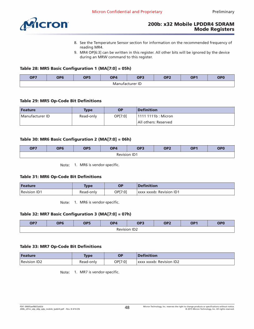
8. See the Temperature Sensor section for information on the recommended frequency ofreading MR4.
9. MR4 OP[6:3] can be written in this register. All other bits will be ignored by the deviceduring an MRW command to this register.
Table 28: MR5 Basic Configuration 1 (MA[7:0] = 05h)
OP7 OP6 OP5 OP4 OP3 OP2 OP1 OP0
Manufacturer ID
Table 29: MR5 Op-Code Bit Definitions
Feature Type OP Definition
Manufacturer ID Read-only OP[7:0] 1111 1111b : Micron
All others: Reserved
Table 30: MR6 Basic Configuration 2 (MA[7:0] = 06h)
OP7 OP6 OP5 OP4 OP3 OP2 OP1 OP0
Revision ID1
Note: 1. MR6 is vendor-specific.
Table 31: MR6 Op-Code Bit Definitions
Feature Type OP Definition
Revision ID1 Read-only OP[7:0] xxxx xxxxb: Revision ID1
Note: 1. MR6 is vendor-specific.
Table 32: MR7 Basic Configuration 3 (MA[7:0] = 07h)
OP7 OP6 OP5 OP4 OP3 OP2 OP1 OP0
Revision ID2
Table 33: MR7 Op-Code Bit Definitions
Feature Type OP Definition
Revision ID2 Read-only OP[7:0] xxxx xxxxb: Revision ID2
Note: 1. MR7 is vendor-specific.
Micron Confidential and Proprietary Preliminary
200b: x32 Mobile LPDDR4 SDRAMMode Registers
PDF: 09005aef8653a92d200b_z01m_sdp_ddp_qdp_mobile_lpddr4.pdf – Rev. B 4/16 EN 48 Micron Technology, Inc. reserves the right to change products or specifications without notice.
© 2015 Micron Technology, Inc. All rights reserved.
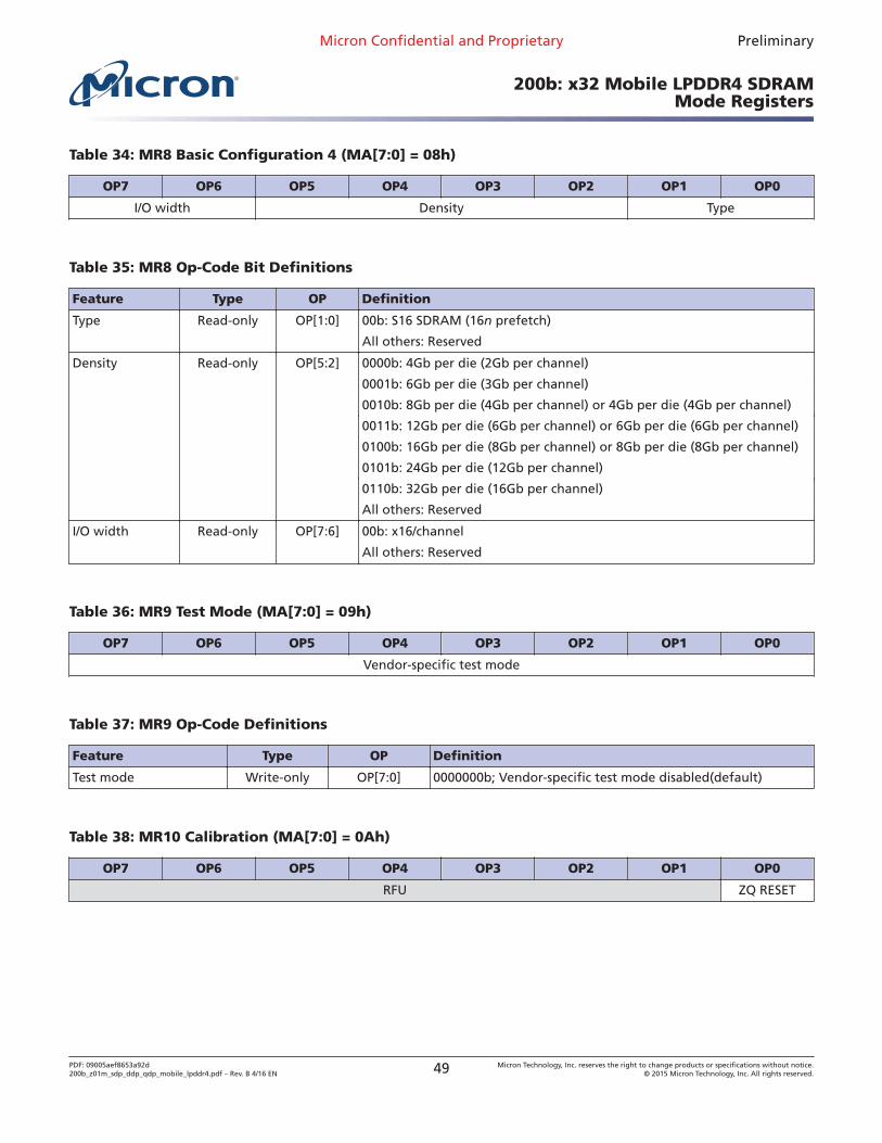
Table 34: MR8 Basic Configuration 4 (MA[7:0] = 08h)
OP7 OP6 OP5 OP4 OP3 OP2 OP1 OP0
I/O width Density Type
Table 35: MR8 Op-Code Bit Definitions
Feature Type OP Definition
Type Read-only OP[1:0] 00b: S16 SDRAM (16n prefetch)
All others: Reserved
Density Read-only OP[5:2] 0000b: 4Gb per die (2Gb per channel)
0001b: 6Gb per die (3Gb per channel)
0010b: 8Gb per die (4Gb per channel) or 4Gb per die (4Gb per channel)
0011b: 12Gb per die (6Gb per channel) or 6Gb per die (6Gb per channel)
0100b: 16Gb per die (8Gb per channel) or 8Gb per die (8Gb per channel)
0101b: 24Gb per die (12Gb per channel)
0110b: 32Gb per die (16Gb per channel)
All others: Reserved
I/O width Read-only OP[7:6] 00b: x16/channel
All others: Reserved
Table 36: MR9 Test Mode (MA[7:0] = 09h)
OP7 OP6 OP5 OP4 OP3 OP2 OP1 OP0
Vendor-specific test mode
Table 37: MR9 Op-Code Definitions
Feature Type OP Definition
Test mode Write-only OP[7:0] 0000000b; Vendor-specific test mode disabled(default)
Table 38: MR10 Calibration (MA[7:0] = 0Ah)
OP7 OP6 OP5 OP4 OP3 OP2 OP1 OP0
RFU ZQ RESET
Micron Confidential and Proprietary Preliminary
200b: x32 Mobile LPDDR4 SDRAMMode Registers
PDF: 09005aef8653a92d200b_z01m_sdp_ddp_qdp_mobile_lpddr4.pdf – Rev. B 4/16 EN 49 Micron Technology, Inc. reserves the right to change products or specifications without notice.
© 2015 Micron Technology, Inc. All rights reserved.
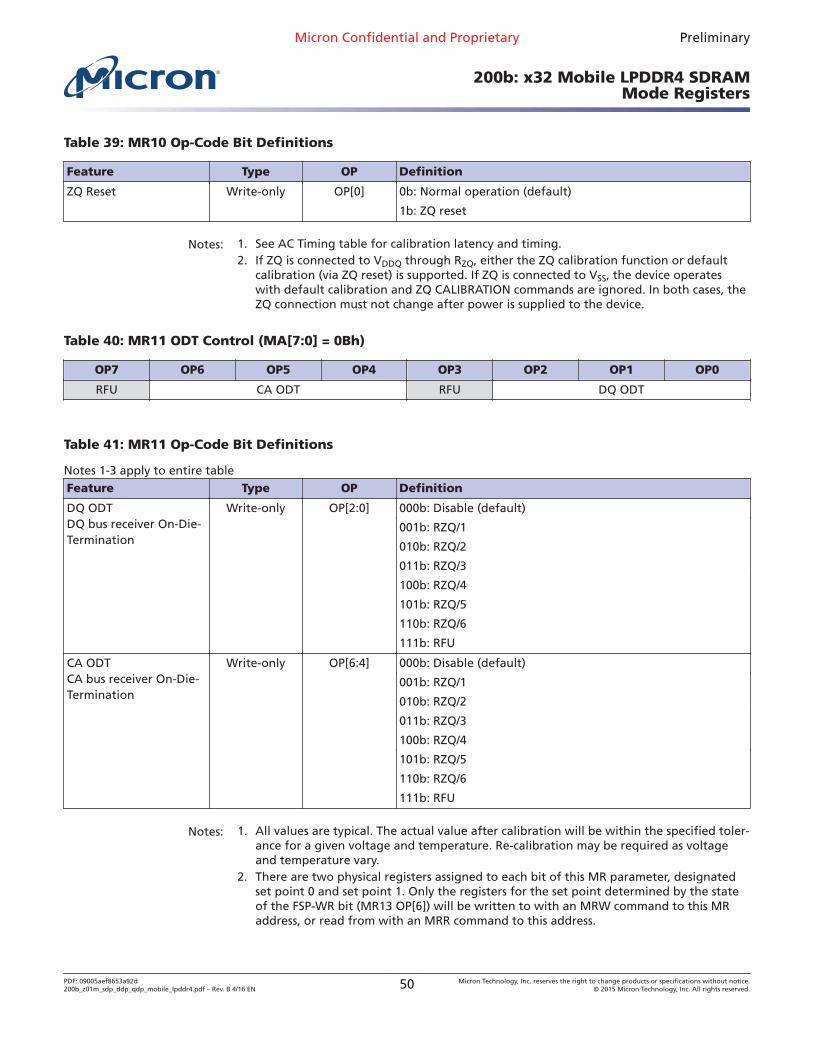
Table 39: MR10 Op-Code Bit Definitions
Feature Type OP Definition
ZQ Reset Write-only OP[0] 0b: Normal operation (default)
1b: ZQ reset
Notes: 1. See AC Timing table for calibration latency and timing.2. If ZQ is connected to VDDQ through RZQ, either the ZQ calibration function or default
calibration (via ZQ reset) is supported. If ZQ is connected to VSS, the device operateswith default calibration and ZQ CALIBRATION commands are ignored. In both cases, theZQ connection must not change after power is supplied to the device.
Table 40: MR11 ODT Control (MA[7:0] = 0Bh)
OP7 OP6 OP5 OP4 OP3 OP2 OP1 OP0
RFU CA ODT RFU DQ ODT
Table 41: MR11 Op-Code Bit Definitions
Notes 1-3 apply to entire tableFeature Type OP Definition
DQ ODTDQ bus receiver On-Die-Termination
Write-only OP[2:0] 000b: Disable (default)
001b: RZQ/1
010b: RZQ/2
011b: RZQ/3
100b: RZQ/4
101b: RZQ/5
110b: RZQ/6
111b: RFU
CA ODTCA bus receiver On-Die-Termination
Write-only OP[6:4] 000b: Disable (default)
001b: RZQ/1
010b: RZQ/2
011b: RZQ/3
100b: RZQ/4
101b: RZQ/5
110b: RZQ/6
111b: RFU
Notes: 1. All values are typical. The actual value after calibration will be within the specified toler-ance for a given voltage and temperature. Re‐calibration may be required as voltageand temperature vary.
2. There are two physical registers assigned to each bit of this MR parameter, designatedset point 0 and set point 1. Only the registers for the set point determined by the stateof the FSP‐WR bit (MR13 OP[6]) will be written to with an MRW command to this MRaddress, or read from with an MRR command to this address.
Micron Confidential and Proprietary Preliminary
200b: x32 Mobile LPDDR4 SDRAMMode Registers
PDF: 09005aef8653a92d200b_z01m_sdp_ddp_qdp_mobile_lpddr4.pdf – Rev. B 4/16 EN 50 Micron Technology, Inc. reserves the right to change products or specifications without notice.
© 2015 Micron Technology, Inc. All rights reserved.
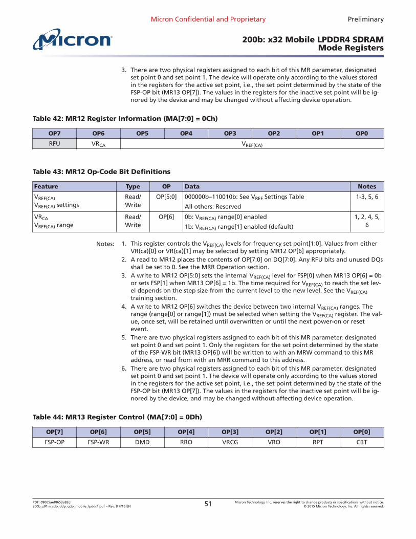
3. There are two physical registers assigned to each bit of this MR parameter, designatedset point 0 and set point 1. The device will operate only according to the values storedin the registers for the active set point, i.e., the set point determined by the state of theFSP‐OP bit (MR13 OP[7]). The values in the registers for the inactive set point will be ig-nored by the device and may be changed without affecting device operation.
Table 42: MR12 Register Information (MA[7:0] = 0Ch)
OP7 OP6 OP5 OP4 OP3 OP2 OP1 OP0
RFU VRCA VREF(CA)
Table 43: MR12 Op-Code Bit Definitions
Feature Type OP Data Notes
VREF(CA)
VREF(CA) settingsRead/Write
OP[5:0] 000000b–110010b: See VREF Settings Table 1-3, 5, 6
All others: Reserved
VRCA
VREF(CA) rangeRead/Write
OP[6] 0b: VREF(CA) range[0] enabled 1, 2, 4, 5,61b: VREF(CA) range[1] enabled (default)
Notes: 1. This register controls the VREF(CA) levels for frequency set point[1:0]. Values from eitherVR(ca)[0] or VR(ca)[1] may be selected by setting MR12 OP[6] appropriately.
2. A read to MR12 places the contents of OP[7:0] on DQ[7:0]. Any RFU bits and unused DQsshall be set to 0. See the MRR Operation section.
3. A write to MR12 OP[5:0] sets the internal VREF(CA) level for FSP[0] when MR13 OP[6] = 0bor sets FSP[1] when MR13 OP[6] = 1b. The time required for VREF(CA) to reach the set lev-el depends on the step size from the current level to the new level. See the VREF(CA)training section.
4. A write to MR12 OP[6] switches the device between two internal VREF(CA) ranges. Therange (range[0] or range[1]) must be selected when setting the VREF(CA) register. The val-ue, once set, will be retained until overwritten or until the next power‐on or resetevent.
5. There are two physical registers assigned to each bit of this MR parameter, designatedset point 0 and set point 1. Only the registers for the set point determined by the stateof the FSP‐WR bit (MR13 OP[6]) will be written to with an MRW command to this MRaddress, or read from with an MRR command to this address.
6. There are two physical registers assigned to each bit of this MR parameter, designatedset point 0 and set point 1. The device will operate only according to the values storedin the registers for the active set point, i.e., the set point determined by the state of theFSP‐OP bit (MR13 OP[7]). The values in the registers for the inactive set point will be ig-nored by the device, and may be changed without affecting device operation.
Table 44: MR13 Register Control (MA[7:0] = 0Dh)
OP[7] OP[6] OP[5] OP[4] OP[3] OP[2] OP[1] OP[0]
FSP-OP FSP-WR DMD RRO VRCG VRO RPT CBT
Micron Confidential and Proprietary Preliminary
200b: x32 Mobile LPDDR4 SDRAMMode Registers
PDF: 09005aef8653a92d200b_z01m_sdp_ddp_qdp_mobile_lpddr4.pdf – Rev. B 4/16 EN 51 Micron Technology, Inc. reserves the right to change products or specifications without notice.
© 2015 Micron Technology, Inc. All rights reserved.
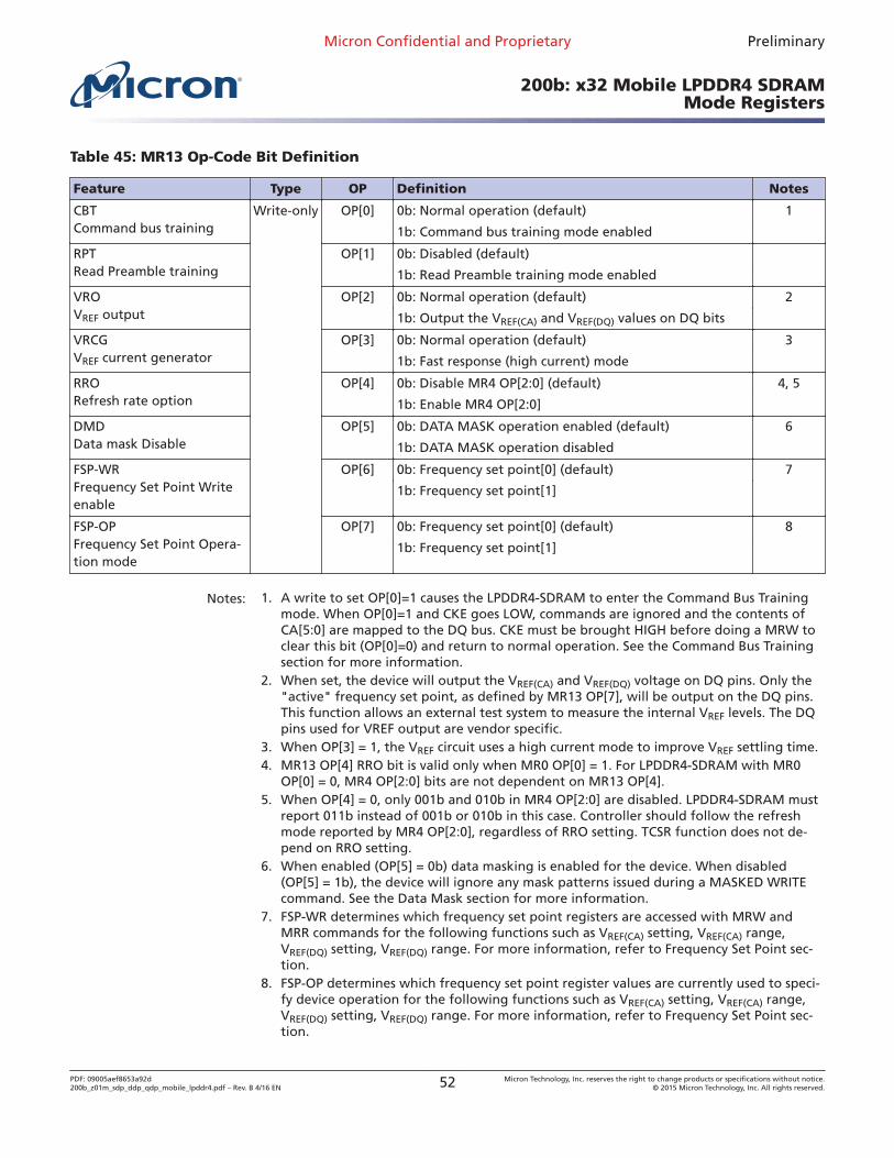
Table 45: MR13 Op-Code Bit Definition
Feature Type OP Definition Notes
CBTCommand bus training
Write-only OP[0] 0b: Normal operation (default) 1
1b: Command bus training mode enabled
RPTRead Preamble training
OP[1] 0b: Disabled (default)
1b: Read Preamble training mode enabled
VROVREF output
OP[2] 0b: Normal operation (default) 2
1b: Output the VREF(CA) and VREF(DQ) values on DQ bits
VRCGVREF current generator
OP[3] 0b: Normal operation (default) 3
1b: Fast response (high current) mode
RRORefresh rate option
OP[4] 0b: Disable MR4 OP[2:0] (default) 4, 5
1b: Enable MR4 OP[2:0]
DMDData mask Disable
OP[5] 0b: DATA MASK operation enabled (default) 6
1b: DATA MASK operation disabled
FSP-WRFrequency Set Point Writeenable
OP[6] 0b: Frequency set point[0] (default) 7
1b: Frequency set point[1]
FSP-OPFrequency Set Point Opera-tion mode
OP[7] 0b: Frequency set point[0] (default) 8
1b: Frequency set point[1]
Notes: 1. A write to set OP[0]=1 causes the LPDDR4‐SDRAM to enter the Command Bus Trainingmode. When OP[0]=1 and CKE goes LOW, commands are ignored and the contents ofCA[5:0] are mapped to the DQ bus. CKE must be brought HIGH before doing a MRW toclear this bit (OP[0]=0) and return to normal operation. See the Command Bus Trainingsection for more information.
2. When set, the device will output the VREF(CA) and VREF(DQ) voltage on DQ pins. Only the"active" frequency set point, as defined by MR13 OP[7], will be output on the DQ pins.This function allows an external test system to measure the internal VREF levels. The DQpins used for VREF output are vendor specific.
3. When OP[3] = 1, the VREF circuit uses a high current mode to improve VREF settling time.4. MR13 OP[4] RRO bit is valid only when MR0 OP[0] = 1. For LPDDR4‐SDRAM with MR0
OP[0] = 0, MR4 OP[2:0] bits are not dependent on MR13 OP[4].5. When OP[4] = 0, only 001b and 010b in MR4 OP[2:0] are disabled. LPDDR4‐SDRAM must
report 011b instead of 001b or 010b in this case. Controller should follow the refreshmode reported by MR4 OP[2:0], regardless of RRO setting. TCSR function does not de-pend on RRO setting.
6. When enabled (OP[5] = 0b) data masking is enabled for the device. When disabled(OP[5] = 1b), the device will ignore any mask patterns issued during a MASKED WRITEcommand. See the Data Mask section for more information.
7. FSP‐WR determines which frequency set point registers are accessed with MRW andMRR commands for the following functions such as VREF(CA) setting, VREF(CA) range,VREF(DQ) setting, VREF(DQ) range. For more information, refer to Frequency Set Point sec-tion.
8. FSP‐OP determines which frequency set point register values are currently used to speci-fy device operation for the following functions such as VREF(CA) setting, VREF(CA) range,VREF(DQ) setting, VREF(DQ) range. For more information, refer to Frequency Set Point sec-tion.
Micron Confidential and Proprietary Preliminary
200b: x32 Mobile LPDDR4 SDRAMMode Registers
PDF: 09005aef8653a92d200b_z01m_sdp_ddp_qdp_mobile_lpddr4.pdf – Rev. B 4/16 EN 52 Micron Technology, Inc. reserves the right to change products or specifications without notice.
© 2015 Micron Technology, Inc. All rights reserved.
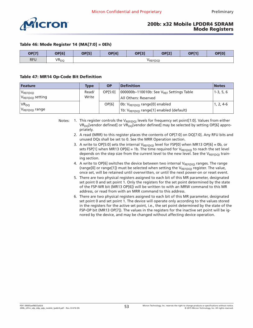
Table 46: Mode Register 14 (MA[7:0] = 0Eh)
OP[7] OP[6] OP[5] OP[4] OP[3] OP[2] OP[1] OP[0]
RFU VRDQ VREF(DQ)
Table 47: MR14 Op-Code Bit Definition
Feature Type OP Definition Notes
VREF(DQ)
VREF(DQ) settingRead/Write
OP[5:0] 000000b–110010b: See VREF Settings Table 1-3, 5, 6
All Others: Reserved
VRDQ
VREF(DQ) rangeOP[6] 0b: VREF(DQ) range[0] enabled 1, 2, 4-6
1b: VREF(DQ) range[1] enabled (default)
Notes: 1. This register controls the VREF(DQ) levels for frequency set point[1:0]. Values from eitherVRDQ[vendor defined] or VRDQ[vendor defined] may be selected by setting OP[6] appro-priately.
2. A read (MRR) to this register places the contents of OP[7:0] on DQ[7:0]. Any RFU bits andunused DQs shall be set to 0. See the MRR Operation section.
3. A write to OP[5:0] sets the internal VREF(DQ) level for FSP[0] when MR13 OP[6] = 0b, orsets FSP[1] when MR13 OP[6] = 1b. The time required for VREF(DQ) to reach the set leveldepends on the step size from the current level to the new level. See the VREF(DQ) train-ing section.
4. A write to OP[6] switches the device between two internal VREF(DQ) ranges. The range(range[0] or range[1]) must be selected when setting the VREF(DQ) register. The value,once set, will be retained until overwritten, or until the next power‐on or reset event.
5. There are two physical registers assigned to each bit of this MR parameter, designatedset point 0 and set point 1. Only the registers for the set point determined by the stateof the FSP‐WR bit (MR13 OP[6]) will be written to with an MRW command to this MRaddress, or read from with an MRR command to this address.
6. There are two physical registers assigned to each bit of this MR parameter, designatedset point 0 and set point 1. The device will operate only according to the values storedin the registers for the active set point, i.e., the set point determined by the state of theFSP‐OP bit (MR13 OP[7]). The values in the registers for the inactive set point will be ig-nored by the device, and may be changed without affecting device operation.
Micron Confidential and Proprietary Preliminary
200b: x32 Mobile LPDDR4 SDRAMMode Registers
PDF: 09005aef8653a92d200b_z01m_sdp_ddp_qdp_mobile_lpddr4.pdf – Rev. B 4/16 EN 53 Micron Technology, Inc. reserves the right to change products or specifications without notice.
© 2015 Micron Technology, Inc. All rights reserved.
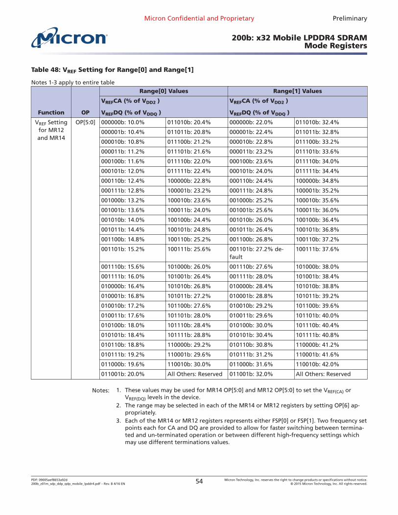
Table 48: VREF Setting for Range[0] and Range[1]
Notes 1-3 apply to entire table
Function OP
Range[0] Values Range[1] Values
VREFCA (% of VDD2 )
VREFDQ (% of VDDQ )
VREFCA (% of VDD2 )
VREFDQ (% of VDDQ )
VREF Settingfor MR12and MR14
OP[5:0] 000000b: 10.0% 011010b: 20.4% 000000b: 22.0% 011010b: 32.4%
000001b: 10.4% 011011b: 20.8% 000001b: 22.4% 011011b: 32.8%
000010b: 10.8% 011100b: 21.2% 000010b: 22.8% 011100b: 33.2%
000011b: 11.2% 011101b: 21.6% 000011b: 23.2% 011101b: 33.6%
000100b: 11.6% 011110b: 22.0% 000100b: 23.6% 011110b: 34.0%
000101b: 12.0% 011111b: 22.4% 000101b: 24.0% 011111b: 34.4%
000110b: 12.4% 100000b: 22.8% 000110b: 24.4% 100000b: 34.8%
000111b: 12.8% 100001b: 23.2% 000111b: 24.8% 100001b: 35.2%
001000b: 13.2% 100010b: 23.6% 001000b: 25.2% 100010b: 35.6%
001001b: 13.6% 100011b: 24.0% 001001b: 25.6% 100011b: 36.0%
001010b: 14.0% 100100b: 24.4% 001010b: 26.0% 100100b: 36.4%
001011b: 14.4% 100101b: 24.8% 001011b: 26.4% 100101b: 36.8%
001100b: 14.8% 100110b: 25.2% 001100b: 26.8% 100110b: 37.2%
001101b: 15.2% 100111b: 25.6% 001101b: 27.2% de-fault
100111b: 37.6%
001110b: 15.6% 101000b: 26.0% 001110b: 27.6% 101000b: 38.0%
001111b: 16.0% 101001b: 26.4% 001111b: 28.0% 101001b: 38.4%
010000b: 16.4% 101010b: 26.8% 010000b: 28.4% 101010b: 38.8%
010001b: 16.8% 101011b: 27.2% 010001b: 28.8% 101011b: 39.2%
010010b: 17.2% 101100b: 27.6% 010010b: 29.2% 101100b: 39.6%
010011b: 17.6% 101101b: 28.0% 010011b: 29.6% 101101b: 40.0%
010100b: 18.0% 101110b: 28.4% 010100b: 30.0% 101110b: 40.4%
010101b: 18.4% 101111b: 28.8% 010101b: 30.4% 101111b: 40.8%
010110b: 18.8% 110000b: 29.2% 010110b: 30.8% 110000b: 41.2%
010111b: 19.2% 110001b: 29.6% 010111b: 31.2% 110001b: 41.6%
011000b: 19.6% 110010b: 30.0% 011000b: 31.6% 110010b: 42.0%
011001b: 20.0% All Others: Reserved 011001b: 32.0% All Others: Reserved
Notes: 1. These values may be used for MR14 OP[5:0] and MR12 OP[5:0] to set the VREF(CA) orVREF(DQ) levels in the device.
2. The range may be selected in each of the MR14 or MR12 registers by setting OP[6] ap-propriately.
3. Each of the MR14 or MR12 registers represents either FSP[0] or FSP[1]. Two frequency setpoints each for CA and DQ are provided to allow for faster switching between termina-ted and un‐terminated operation or between different high‐frequency settings whichmay use different terminations values.
Micron Confidential and Proprietary Preliminary
200b: x32 Mobile LPDDR4 SDRAMMode Registers
PDF: 09005aef8653a92d200b_z01m_sdp_ddp_qdp_mobile_lpddr4.pdf – Rev. B 4/16 EN 54 Micron Technology, Inc. reserves the right to change products or specifications without notice.
© 2015 Micron Technology, Inc. All rights reserved.
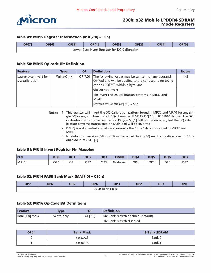
Table 49: MR15 Register Information (MA[7:0] = 0Fh)
OP[7] OP[6] OP[5] OP[4] OP[3] OP[2] OP[1] OP[0]
Lower-Byte Invert Register for DQ Calibration
Table 50: MR15 Op-code Bit Definition
Feature Type OP Definition Notes
Lower-byte invert forDQ calibration
Write-Only OP[7:0] The following values may be written for any operandOP[7:0] and will be applied to the corresponding DQ lo-cations DQ[7:0] within a byte lane
1–3
0b: Do not invert
1b: Invert the DQ calibration patterns in MR32 andMR40
Default value for OP[7:0] = 55h
Notes: 1. This register will invert the DQ Calibration pattern found in MR32 and MR40 for any sin-gle DQ or any combination of DQs. Example: If MR15 OP[7:0] = 00010101b, then the DQcalibration patterns transmitted on DQ[7,6,5,3,1] will not be inverted, but the DQ cali-bration patterns transmitted on DQ[4,2,0] will be inverted.
2. DM[0] is not inverted and always transmits the "true" data contained in MR32 andMR40.
3. No data bus inversion (DBI) function is enacted during DQ read calibration, even if DBI isenabled in MR3-OP[6].
Table 51: MR15 Invert Register Pin Mapping
PIN DQ0 DQ1 DQ2 DQ3 DMIO DQ4 DQ5 DQ6 DQ7
MR15 OP0 OP1 OP2 OP3 No-Invert OP4 OP5 OP6 OP7
Table 52: MR16 PASR Bank Mask (MA[7:0] = 010h)
OP7 OP6 OP5 OP4 OP3 OP2 OP1 OP0
PASR Bank Mask
Table 53: MR16 Op-Code Bit Definitions
Feature Type OP Definition
Bank[7:0] mask Write-only OP[7:0] 0b: Bank refresh enabled (default)
1b: Bank refresh disabled
OP[n] Bank Mask 8-Bank SDRAM
0 xxxxxxx1 Bank 0
1 xxxxxx1x Bank 1
Micron Confidential and Proprietary Preliminary
200b: x32 Mobile LPDDR4 SDRAMMode Registers
PDF: 09005aef8653a92d200b_z01m_sdp_ddp_qdp_mobile_lpddr4.pdf – Rev. B 4/16 EN 55 Micron Technology, Inc. reserves the right to change products or specifications without notice.
© 2015 Micron Technology, Inc. All rights reserved.
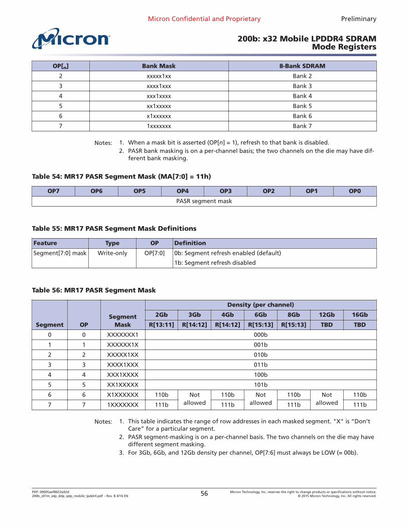
OP[n] Bank Mask 8-Bank SDRAM
2 xxxxx1xx Bank 2
3 xxxx1xxx Bank 3
4 xxx1xxxx Bank 4
5 xx1xxxxx Bank 5
6 x1xxxxxx Bank 6
7 1xxxxxxx Bank 7
Notes: 1. When a mask bit is asserted (OP[n] = 1), refresh to that bank is disabled.2. PASR bank masking is on a per-channel basis; the two channels on the die may have dif-
ferent bank masking.
Table 54: MR17 PASR Segment Mask (MA[7:0] = 11h)
OP7 OP6 OP5 OP4 OP3 OP2 OP1 OP0
PASR segment mask
Table 55: MR17 PASR Segment Mask Definitions
Feature Type OP Definition
Segment[7:0] mask Write-only OP[7:0] 0b: Segment refresh enabled (default)
1b: Segment refresh disabled
Table 56: MR17 PASR Segment Mask
Segment OPSegment
Mask
Density (per channel)
2Gb 3Gb 4Gb 6Gb 8Gb 12Gb 16Gb
R[13:11] R[14:12] R[14:12] R[15:13] R[15:13] TBD TBD
0 0 XXXXXXX1 000b
1 1 XXXXXX1X 001b
2 2 XXXXX1XX 010b
3 3 XXXX1XXX 011b
4 4 XXX1XXXX 100b
5 5 XX1XXXXX 101b
6 6 X1XXXXXX 110b Notallowed
110b Notallowed
110b Notallowed
110b
7 7 1XXXXXXX 111b 111b 111b 111b
Notes: 1. This table indicates the range of row addresses in each masked segment. "X" is “Don’tCare” for a particular segment.
2. PASR segment-masking is on a per-channel basis. The two channels on the die may havedifferent segment masking.
3. For 3Gb, 6Gb, and 12Gb density per channel, OP[7:6] must always be LOW (= 00b).
Micron Confidential and Proprietary Preliminary
200b: x32 Mobile LPDDR4 SDRAMMode Registers
PDF: 09005aef8653a92d200b_z01m_sdp_ddp_qdp_mobile_lpddr4.pdf – Rev. B 4/16 EN 56 Micron Technology, Inc. reserves the right to change products or specifications without notice.
© 2015 Micron Technology, Inc. All rights reserved.
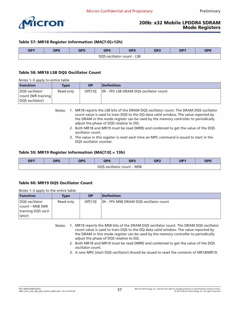
Table 57: MR18 Register Information (MA[7:0]=12h)
OP7 OP6 OP5 OP4 OP3 OP2 OP1 OP0
DQS oscillator count - LSB
Table 58: MR18 LSB DQS Oscillator Count
Notes 1–3 apply to entire tableFunction Type OP Definition
DQS oscillatorcount (WR trainingDQS oscillator)
Read-only OP[7:0] 0h - FFh LSB DRAM DQS oscillator count
Notes: 1. MR18 reports the LSB bits of the DRAM DQS oscillator count. The DRAM DQS oscillatorcount value is used to train DQS to the DQ data valid window. The value reported bythe DRAM in this mode register can be used by the memory controller to periodicallyadjust the phase of DQS relative to DQ.
2. Both MR18 and MR19 must be read (MRR) and combined to get the value of the DQSoscillator count.
3. The value in this register is reset each time an MPC command is issued to start in theDQS oscillator counter.
Table 59: MR19 Register Information (MA[7:0] = 13h)
OP7 OP6 OP5 OP4 OP3 OP2 OP1 OP0
DQS oscillator count – MSB
Table 60: MR19 DQS Oscillator Count
Notes 1–3 apply to the entire tableFunction Type OP Definition
DQS oscillatorcount – MSB (WRtraining DQS oscil-lator)
Read-only OP[7:0] 0h - FFh MSB DRAM DQS oscillator count
Notes: 1. MR19 reports the MSB bits of the DRAM DQS oscillator count. The DRAM DQS oscillatorcount value is used to train DQS to the DQ data valid window. The value reported bythe DRAM in this mode register can be used by the memory controller to periodicallyadjust the phase of DQS relative to DQ.
2. Both MR18 and MR19 must be read (MRR) and combined to get the value of the DQSoscillator count.
3. A new MPC [start DQS oscillator] should be issued to reset the contents of MR18/MR19.
Micron Confidential and Proprietary Preliminary
200b: x32 Mobile LPDDR4 SDRAMMode Registers
PDF: 09005aef8653a92d200b_z01m_sdp_ddp_qdp_mobile_lpddr4.pdf – Rev. B 4/16 EN 57 Micron Technology, Inc. reserves the right to change products or specifications without notice.
© 2015 Micron Technology, Inc. All rights reserved.
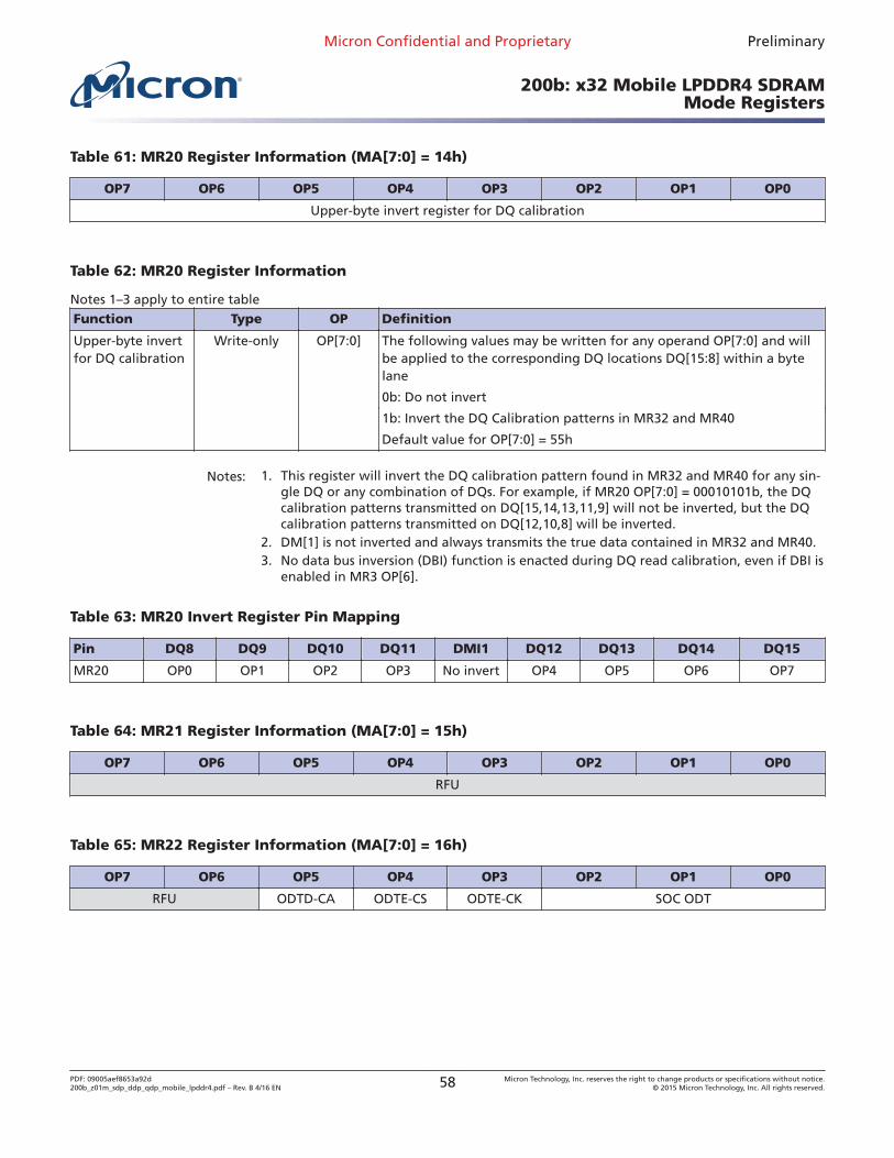
Table 61: MR20 Register Information (MA[7:0] = 14h)
OP7 OP6 OP5 OP4 OP3 OP2 OP1 OP0
Upper-byte invert register for DQ calibration
Table 62: MR20 Register Information
Notes 1–3 apply to entire tableFunction Type OP Definition
Upper-byte invertfor DQ calibration
Write-only OP[7:0] The following values may be written for any operand OP[7:0] and willbe applied to the corresponding DQ locations DQ[15:8] within a bytelane
0b: Do not invert
1b: Invert the DQ Calibration patterns in MR32 and MR40
Default value for OP[7:0] = 55h
Notes: 1. This register will invert the DQ calibration pattern found in MR32 and MR40 for any sin-gle DQ or any combination of DQs. For example, if MR20 OP[7:0] = 00010101b, the DQcalibration patterns transmitted on DQ[15,14,13,11,9] will not be inverted, but the DQcalibration patterns transmitted on DQ[12,10,8] will be inverted.
2. DM[1] is not inverted and always transmits the true data contained in MR32 and MR40.3. No data bus inversion (DBI) function is enacted during DQ read calibration, even if DBI is
enabled in MR3 OP[6].
Table 63: MR20 Invert Register Pin Mapping
Pin DQ8 DQ9 DQ10 DQ11 DMI1 DQ12 DQ13 DQ14 DQ15
MR20 OP0 OP1 OP2 OP3 No invert OP4 OP5 OP6 OP7
Table 64: MR21 Register Information (MA[7:0] = 15h)
OP7 OP6 OP5 OP4 OP3 OP2 OP1 OP0
RFU
Table 65: MR22 Register Information (MA[7:0] = 16h)
OP7 OP6 OP5 OP4 OP3 OP2 OP1 OP0
RFU ODTD-CA ODTE-CS ODTE-CK SOC ODT
Micron Confidential and Proprietary Preliminary
200b: x32 Mobile LPDDR4 SDRAMMode Registers
PDF: 09005aef8653a92d200b_z01m_sdp_ddp_qdp_mobile_lpddr4.pdf – Rev. B 4/16 EN 58 Micron Technology, Inc. reserves the right to change products or specifications without notice.
© 2015 Micron Technology, Inc. All rights reserved.
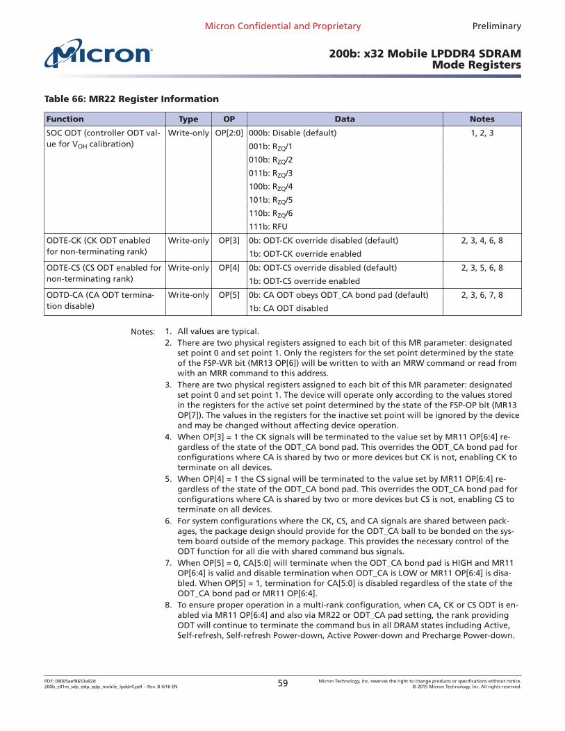
Table 66: MR22 Register Information
Function Type OP Data Notes
SOC ODT (controller ODT val-ue for VOH calibration)
Write-only OP[2:0] 000b: Disable (default) 1, 2, 3
001b: RZQ/1
010b: RZQ/2
011b: RZQ/3
100b: RZQ/4
101b: RZQ/5
110b: RZQ/6
111b: RFU
ODTE-CK (CK ODT enabledfor non-terminating rank)
Write-only OP[3] 0b: ODT-CK override disabled (default) 2, 3, 4, 6, 8
1b: ODT-CK override enabled
ODTE-CS (CS ODT enabled fornon-terminating rank)
Write-only OP[4] 0b: ODT-CS override disabled (default) 2, 3, 5, 6, 8
1b: ODT-CS override enabled
ODTD-CA (CA ODT termina-tion disable)
Write-only OP[5] 0b: CA ODT obeys ODT_CA bond pad (default) 2, 3, 6, 7, 8
1b: CA ODT disabled
Notes: 1. All values are typical.2. There are two physical registers assigned to each bit of this MR parameter: designated
set point 0 and set point 1. Only the registers for the set point determined by the stateof the FSP-WR bit (MR13 OP[6]) will be written to with an MRW command or read fromwith an MRR command to this address.
3. There are two physical registers assigned to each bit of this MR parameter: designatedset point 0 and set point 1. The device will operate only according to the values storedin the registers for the active set point determined by the state of the FSP-OP bit (MR13OP[7]). The values in the registers for the inactive set point will be ignored by the deviceand may be changed without affecting device operation.
4. When OP[3] = 1 the CK signals will be terminated to the value set by MR11 OP[6:4] re-gardless of the state of the ODT_CA bond pad. This overrides the ODT_CA bond pad forconfigurations where CA is shared by two or more devices but CK is not, enabling CK toterminate on all devices.
5. When OP[4] = 1 the CS signal will be terminated to the value set by MR11 OP[6:4] re-gardless of the state of the ODT_CA bond pad. This overrides the ODT_CA bond pad forconfigurations where CA is shared by two or more devices but CS is not, enabling CS toterminate on all devices.
6. For system configurations where the CK, CS, and CA signals are shared between pack-ages, the package design should provide for the ODT_CA ball to be bonded on the sys-tem board outside of the memory package. This provides the necessary control of theODT function for all die with shared command bus signals.
7. When OP[5] = 0, CA[5:0] will terminate when the ODT_CA bond pad is HIGH and MR11OP[6:4] is valid and disable termination when ODT_CA is LOW or MR11 OP[6:4] is disa-bled. When OP[5] = 1, termination for CA[5:0] is disabled regardless of the state of theODT_CA bond pad or MR11 OP[6:4].
8. To ensure proper operation in a multi-rank configuration, when CA, CK or CS ODT is en-abled via MR11 OP[6:4] and also via MR22 or ODT_CA pad setting, the rank providingODT will continue to terminate the command bus in all DRAM states including Active,Self-refresh, Self-refresh Power-down, Active Power-down and Precharge Power-down.
Micron Confidential and Proprietary Preliminary
200b: x32 Mobile LPDDR4 SDRAMMode Registers
PDF: 09005aef8653a92d200b_z01m_sdp_ddp_qdp_mobile_lpddr4.pdf – Rev. B 4/16 EN 59 Micron Technology, Inc. reserves the right to change products or specifications without notice.
© 2015 Micron Technology, Inc. All rights reserved.
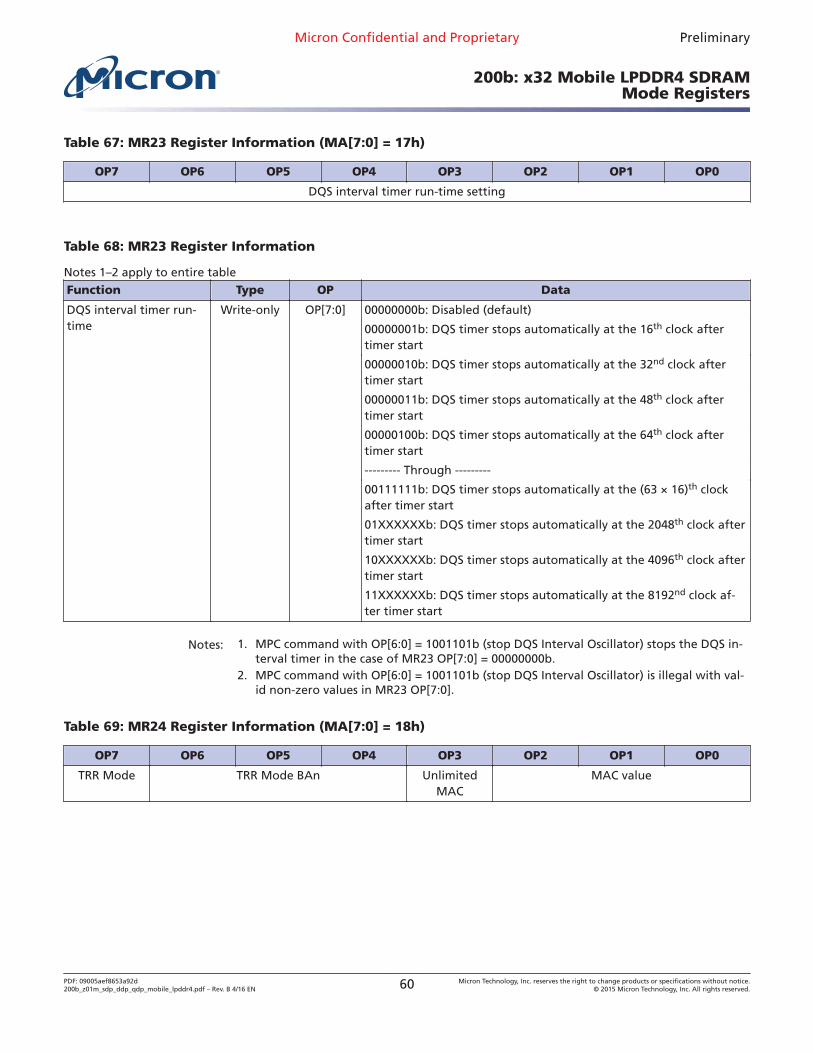
Table 67: MR23 Register Information (MA[7:0] = 17h)
OP7 OP6 OP5 OP4 OP3 OP2 OP1 OP0
DQS interval timer run-time setting
Table 68: MR23 Register Information
Notes 1–2 apply to entire tableFunction Type OP Data
DQS interval timer run-time
Write-only OP[7:0] 00000000b: Disabled (default)
00000001b: DQS timer stops automatically at the 16th clock aftertimer start
00000010b: DQS timer stops automatically at the 32nd clock aftertimer start
00000011b: DQS timer stops automatically at the 48th clock aftertimer start
00000100b: DQS timer stops automatically at the 64th clock aftertimer start
--------- Through ---------
00111111b: DQS timer stops automatically at the (63 × 16)th clockafter timer start
01XXXXXXb: DQS timer stops automatically at the 2048th clock aftertimer start
10XXXXXXb: DQS timer stops automatically at the 4096th clock aftertimer start
11XXXXXXb: DQS timer stops automatically at the 8192nd clock af-ter timer start
Notes: 1. MPC command with OP[6:0] = 1001101b (stop DQS Interval Oscillator) stops the DQS in-terval timer in the case of MR23 OP[7:0] = 00000000b.
2. MPC command with OP[6:0] = 1001101b (stop DQS Interval Oscillator) is illegal with val-id non-zero values in MR23 OP[7:0].
Table 69: MR24 Register Information (MA[7:0] = 18h)
OP7 OP6 OP5 OP4 OP3 OP2 OP1 OP0
TRR Mode TRR Mode BAn UnlimitedMAC
MAC value
Micron Confidential and Proprietary Preliminary
200b: x32 Mobile LPDDR4 SDRAMMode Registers
PDF: 09005aef8653a92d200b_z01m_sdp_ddp_qdp_mobile_lpddr4.pdf – Rev. B 4/16 EN 60 Micron Technology, Inc. reserves the right to change products or specifications without notice.
© 2015 Micron Technology, Inc. All rights reserved.
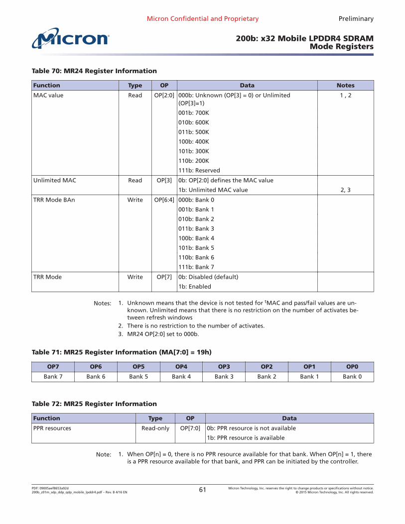
Table 70: MR24 Register Information
Function Type OP Data Notes
MAC value Read OP[2:0] 000b: Unknown (OP[3] = 0) or Unlimited(OP[3]=1)
1 , 2
001b: 700K
010b: 600K
011b: 500K
100b: 400K
101b: 300K
110b: 200K
111b: Reserved
Unlimited MAC Read OP[3] 0b: OP[2:0] defines the MAC value
1b: Unlimited MAC value 2, 3
TRR Mode BAn Write OP[6:4] 000b: Bank 0
001b: Bank 1
010b: Bank 2
011b: Bank 3
100b: Bank 4
101b: Bank 5
110b: Bank 6
111b: Bank 7
TRR Mode Write OP[7] 0b: Disabled (default)
1b: Enabled
Notes: 1. Unknown means that the device is not tested for tMAC and pass/fail values are un-known. Unlimited means that there is no restriction on the number of activates be-tween refresh windows
2. There is no restriction to the number of activates.3. MR24 OP[2:0] set to 000b.
Table 71: MR25 Register Information (MA[7:0] = 19h)
OP7 OP6 OP5 OP4 OP3 OP2 OP1 OP0
Bank 7 Bank 6 Bank 5 Bank 4 Bank 3 Bank 2 Bank 1 Bank 0
Table 72: MR25 Register Information
Function Type OP Data
PPR resources Read-only OP[7:0] 0b: PPR resource is not available
1b: PPR resource is available
Note: 1. When OP[n] = 0, there is no PPR resource available for that bank. When OP[n] = 1, thereis a PPR resource available for that bank, and PPR can be initiated by the controller.
Micron Confidential and Proprietary Preliminary
200b: x32 Mobile LPDDR4 SDRAMMode Registers
PDF: 09005aef8653a92d200b_z01m_sdp_ddp_qdp_mobile_lpddr4.pdf – Rev. B 4/16 EN 61 Micron Technology, Inc. reserves the right to change products or specifications without notice.
© 2015 Micron Technology, Inc. All rights reserved.
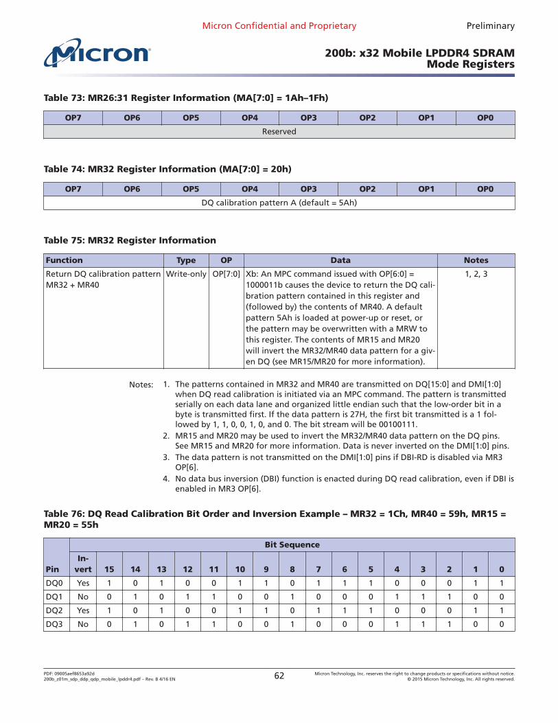
Table 73: MR26:31 Register Information (MA[7:0] = 1Ah–1Fh)
OP7 OP6 OP5 OP4 OP3 OP2 OP1 OP0
Reserved
Table 74: MR32 Register Information (MA[7:0] = 20h)
OP7 OP6 OP5 OP4 OP3 OP2 OP1 OP0
DQ calibration pattern A (default = 5Ah)
Table 75: MR32 Register Information
Function Type OP Data Notes
Return DQ calibration patternMR32 + MR40
Write-only OP[7:0] Xb: An MPC command issued with OP[6:0] =1000011b causes the device to return the DQ cali-bration pattern contained in this register and(followed by) the contents of MR40. A defaultpattern 5Ah is loaded at power-up or reset, orthe pattern may be overwritten with a MRW tothis register. The contents of MR15 and MR20will invert the MR32/MR40 data pattern for a giv-en DQ (see MR15/MR20 for more information).
1, 2, 3
Notes: 1. The patterns contained in MR32 and MR40 are transmitted on DQ[15:0] and DMI[1:0]when DQ read calibration is initiated via an MPC command. The pattern is transmittedserially on each data lane and organized little endian such that the low-order bit in abyte is transmitted first. If the data pattern is 27H, the first bit transmitted is a 1 fol-lowed by 1, 1, 0, 0, 1, 0, and 0. The bit stream will be 00100111.
2. MR15 and MR20 may be used to invert the MR32/MR40 data pattern on the DQ pins.See MR15 and MR20 for more information. Data is never inverted on the DMI[1:0] pins.
3. The data pattern is not transmitted on the DMI[1:0] pins if DBI-RD is disabled via MR3OP[6].
4. No data bus inversion (DBI) function is enacted during DQ read calibration, even if DBI isenabled in MR3 OP[6].
Table 76: DQ Read Calibration Bit Order and Inversion Example – MR32 = 1Ch, MR40 = 59h, MR15 =MR20 = 55h
Pin
Bit Sequence
In-vert 15 14 13 12 11 10 9 8 7 6 5 4 3 2 1 0
DQ0 Yes 1 0 1 0 0 1 1 0 1 1 1 0 0 0 1 1
DQ1 No 0 1 0 1 1 0 0 1 0 0 0 1 1 1 0 0
DQ2 Yes 1 0 1 0 0 1 1 0 1 1 1 0 0 0 1 1
DQ3 No 0 1 0 1 1 0 0 1 0 0 0 1 1 1 0 0
Micron Confidential and Proprietary Preliminary
200b: x32 Mobile LPDDR4 SDRAMMode Registers
PDF: 09005aef8653a92d200b_z01m_sdp_ddp_qdp_mobile_lpddr4.pdf – Rev. B 4/16 EN 62 Micron Technology, Inc. reserves the right to change products or specifications without notice.
© 2015 Micron Technology, Inc. All rights reserved.
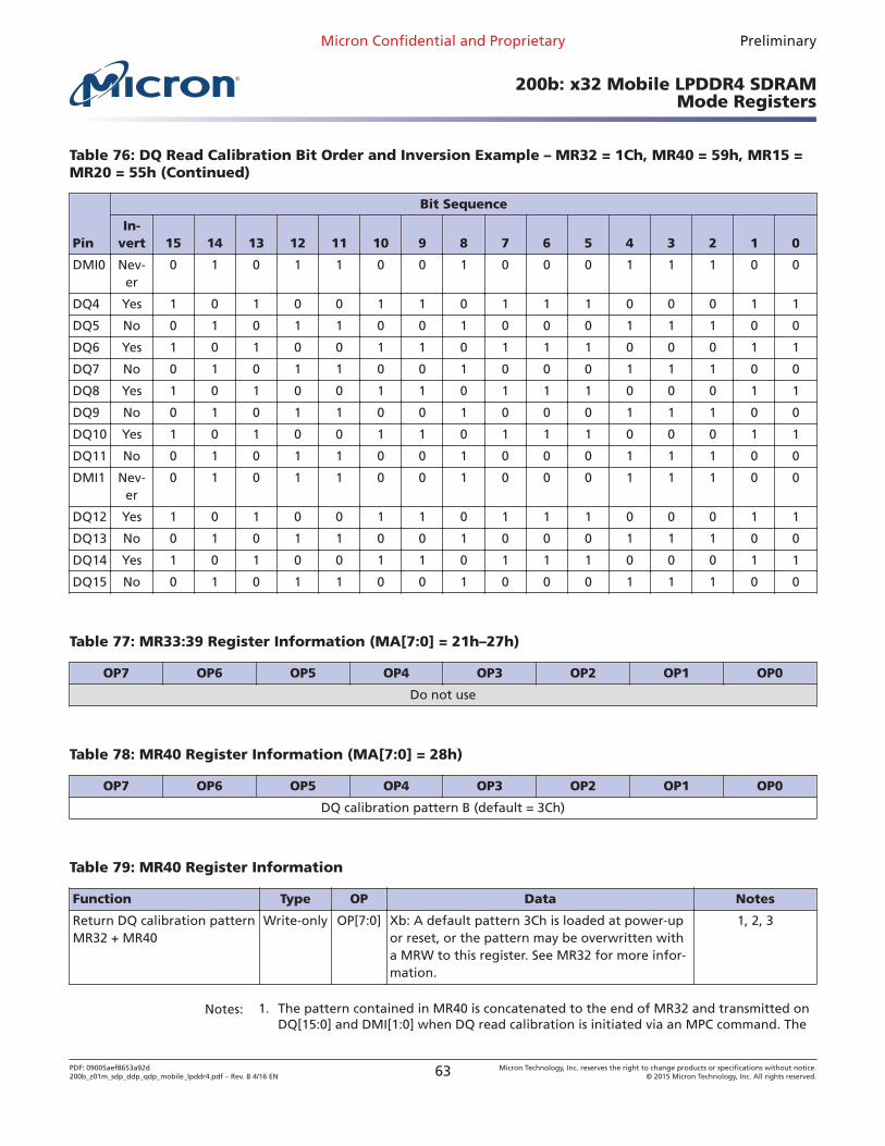
Table 76: DQ Read Calibration Bit Order and Inversion Example – MR32 = 1Ch, MR40 = 59h, MR15 =MR20 = 55h (Continued)
Pin
Bit Sequence
In-vert 15 14 13 12 11 10 9 8 7 6 5 4 3 2 1 0
DMI0 Nev-er
0 1 0 1 1 0 0 1 0 0 0 1 1 1 0 0
DQ4 Yes 1 0 1 0 0 1 1 0 1 1 1 0 0 0 1 1
DQ5 No 0 1 0 1 1 0 0 1 0 0 0 1 1 1 0 0
DQ6 Yes 1 0 1 0 0 1 1 0 1 1 1 0 0 0 1 1
DQ7 No 0 1 0 1 1 0 0 1 0 0 0 1 1 1 0 0
DQ8 Yes 1 0 1 0 0 1 1 0 1 1 1 0 0 0 1 1
DQ9 No 0 1 0 1 1 0 0 1 0 0 0 1 1 1 0 0
DQ10 Yes 1 0 1 0 0 1 1 0 1 1 1 0 0 0 1 1
DQ11 No 0 1 0 1 1 0 0 1 0 0 0 1 1 1 0 0
DMI1 Nev-er
0 1 0 1 1 0 0 1 0 0 0 1 1 1 0 0
DQ12 Yes 1 0 1 0 0 1 1 0 1 1 1 0 0 0 1 1
DQ13 No 0 1 0 1 1 0 0 1 0 0 0 1 1 1 0 0
DQ14 Yes 1 0 1 0 0 1 1 0 1 1 1 0 0 0 1 1
DQ15 No 0 1 0 1 1 0 0 1 0 0 0 1 1 1 0 0
Table 77: MR33:39 Register Information (MA[7:0] = 21h–27h)
OP7 OP6 OP5 OP4 OP3 OP2 OP1 OP0
Do not use
Table 78: MR40 Register Information (MA[7:0] = 28h)
OP7 OP6 OP5 OP4 OP3 OP2 OP1 OP0
DQ calibration pattern B (default = 3Ch)
Table 79: MR40 Register Information
Function Type OP Data Notes
Return DQ calibration patternMR32 + MR40
Write-only OP[7:0] Xb: A default pattern 3Ch is loaded at power-upor reset, or the pattern may be overwritten witha MRW to this register. See MR32 for more infor-mation.
1, 2, 3
Notes: 1. The pattern contained in MR40 is concatenated to the end of MR32 and transmitted onDQ[15:0] and DMI[1:0] when DQ read calibration is initiated via an MPC command. The
Micron Confidential and Proprietary Preliminary
200b: x32 Mobile LPDDR4 SDRAMMode Registers
PDF: 09005aef8653a92d200b_z01m_sdp_ddp_qdp_mobile_lpddr4.pdf – Rev. B 4/16 EN 63 Micron Technology, Inc. reserves the right to change products or specifications without notice.
© 2015 Micron Technology, Inc. All rights reserved.
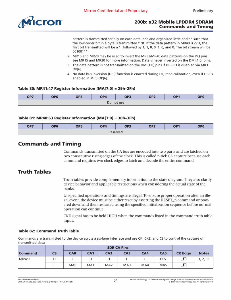
pattern is transmitted serially on each data lane and organized little endian such thatthe low-order bit in a byte is transmitted first. If the data pattern in MR40 is 27H, thefirst bit transmitted will be a 1, followed by 1, 1, 0, 0, 1, 0, and 0. The bit stream will be00100111.
2. MR15 and MR20 may be used to invert the MR32/MR40 data patterns on the DQ pins.See MR15 and MR20 for more information. Data is never inverted on the DMI[1:0] pins.
3. The data pattern is not transmitted on the DMI[1:0] pins if DBI-RD is disabled via MR3OP[6].
4. No data bus inversion (DBI) function is enacted during DQ read calibration, even if DBI isenabled in MR3 OP[6].
Table 80: MR41:47 Register Information (MA[7:0] = 29h–2Fh)
OP7 OP6 OP5 OP4 OP3 OP2 OP1 OP0
Do not use
Table 81: MR48:63 Register Information (MA[7:0] = 30h–3Fh)
OP7 OP6 OP5 OP4 OP3 OP2 OP1 OP0
Reserved
Commands and TimingCommands transmitted on the CA bus are encoded into two parts and are latched ontwo consecutive rising edges of the clock. This is called 2-tick CA capture because eachcommand requires two clock edges to latch and decode the entire command.
Truth TablesTruth tables provide complementary information to the state diagram. They also clarifydevice behavior and applicable restrictions when considering the actual state of thebanks.
Unspecified operations and timings are illegal. To ensure proper operation after an ille-gal event, the device must be either reset by asserting the RESET_n command or pow-ered down and then restarted using the specified initialization sequence before normaloperation can continue.
CKE signal has to be held HIGH when the commands listed in the command truth tableinput.
Table 82: Command Truth Table
Commands are transmitted to the device across a six-lane interface and use CK, CKE, and CS to control the capture oftransmitted data
Command CS
SDR CA Pins
CK Edge NotesCA0 CA1 CA2 CA3 CA4 CA5
MRW-1 H L H H L L OP7 1 1, 2, 11
L MA0 MA1 MA2 MA3 MA4 MA5 2
Micron Confidential and Proprietary Preliminary
200b: x32 Mobile LPDDR4 SDRAMCommands and Timing
PDF: 09005aef8653a92d200b_z01m_sdp_ddp_qdp_mobile_lpddr4.pdf – Rev. B 4/16 EN 64 Micron Technology, Inc. reserves the right to change products or specifications without notice.
© 2015 Micron Technology, Inc. All rights reserved.
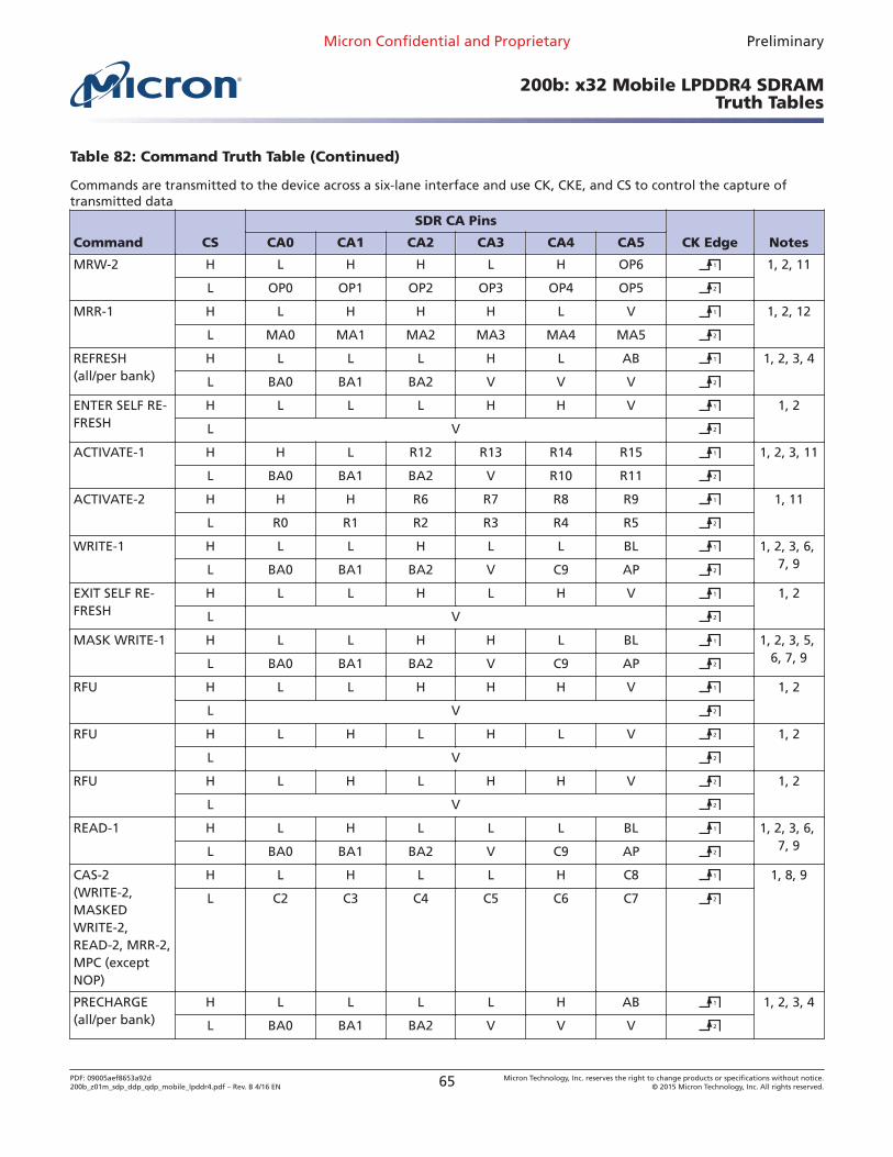
Table 82: Command Truth Table (Continued)
Commands are transmitted to the device across a six-lane interface and use CK, CKE, and CS to control the capture oftransmitted data
Command CS
SDR CA Pins
CK Edge NotesCA0 CA1 CA2 CA3 CA4 CA5
MRW-2 H L H H L H OP6 1 1, 2, 11
L OP0 OP1 OP2 OP3 OP4 OP5 2
MRR-1 H L H H H L V 1 1, 2, 12
L MA0 MA1 MA2 MA3 MA4 MA5 2
REFRESH(all/per bank)
H L L L H L AB 1 1, 2, 3, 4
L BA0 BA1 BA2 V V V 2
ENTER SELF RE-FRESH
H L L L H H V 1 1, 2
L V 2
ACTIVATE-1 H H L R12 R13 R14 R15 1 1, 2, 3, 11
L BA0 BA1 BA2 V R10 R11 2
ACTIVATE-2 H H H R6 R7 R8 R9 1 1, 11
L R0 R1 R2 R3 R4 R5 2
WRITE-1 H L L H L L BL 1 1, 2, 3, 6, 7, 9L BA0 BA1 BA2 V C9 AP 2
EXIT SELF RE-FRESH
H L L H L H V 1 1, 2
L V 2
MASK WRITE-1 H L L H H L BL 1 1, 2, 3, 5, 6, 7, 9L BA0 BA1 BA2 V C9 AP 2
RFU H L L H H H V 1 1, 2
L V 2
RFU H L H L H L V 2 1, 2
L V 2
RFU H L H L H H V 2 1, 2
L V 2
READ-1 H L H L L L BL 1 1, 2, 3, 6, 7, 9L BA0 BA1 BA2 V C9 AP 2
CAS-2(WRITE-2,MASKEDWRITE-2,READ-2, MRR-2,MPC (exceptNOP)
H L H L L H C8 1 1, 8, 9
L C2 C3 C4 C5 C6 C7 2
PRECHARGE(all/per bank)
H L L L L H AB 1 1, 2, 3, 4
L BA0 BA1 BA2 V V V 2
Micron Confidential and Proprietary Preliminary
200b: x32 Mobile LPDDR4 SDRAMTruth Tables
PDF: 09005aef8653a92d200b_z01m_sdp_ddp_qdp_mobile_lpddr4.pdf – Rev. B 4/16 EN 65 Micron Technology, Inc. reserves the right to change products or specifications without notice.
© 2015 Micron Technology, Inc. All rights reserved.
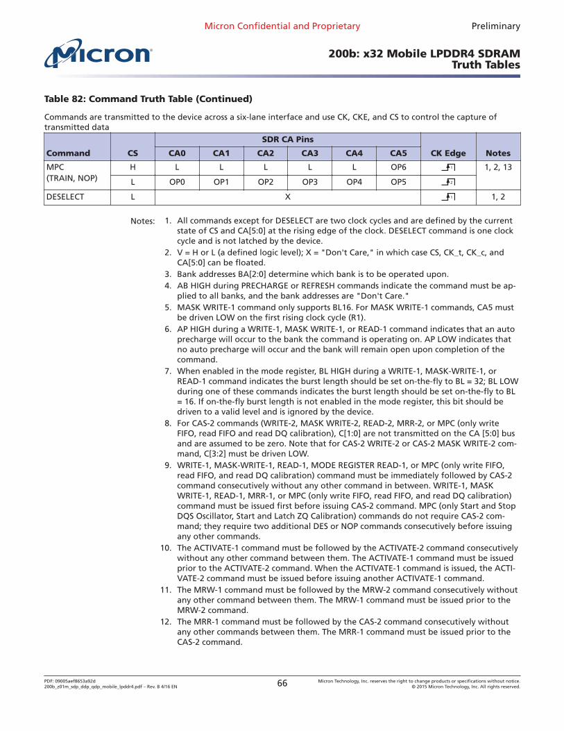
Table 82: Command Truth Table (Continued)
Commands are transmitted to the device across a six-lane interface and use CK, CKE, and CS to control the capture oftransmitted data
Command CS
SDR CA Pins
CK Edge NotesCA0 CA1 CA2 CA3 CA4 CA5
MPC(TRAIN, NOP)
H L L L L L OP6 1 1, 2, 13
L OP0 OP1 OP2 OP3 OP4 OP5 2
DESELECT L X 1 1, 2
Notes: 1. All commands except for DESELECT are two clock cycles and are defined by the currentstate of CS and CA[5:0] at the rising edge of the clock. DESELECT command is one clockcycle and is not latched by the device.
2. V = H or L (a defined logic level); X = "Don't Care," in which case CS, CK_t, CK_c, andCA[5:0] can be floated.
3. Bank addresses BA[2:0] determine which bank is to be operated upon.4. AB HIGH during PRECHARGE or REFRESH commands indicate the command must be ap-
plied to all banks, and the bank addresses are "Don't Care."5. MASK WRITE-1 command only supports BL16. For MASK WRITE-1 commands, CA5 must
be driven LOW on the first rising clock cycle (R1).6. AP HIGH during a WRITE-1, MASK WRITE-1, or READ-1 command indicates that an auto
precharge will occur to the bank the command is operating on. AP LOW indicates thatno auto precharge will occur and the bank will remain open upon completion of thecommand.
7. When enabled in the mode register, BL HIGH during a WRITE-1, MASK-WRITE-1, orREAD-1 command indicates the burst length should be set on-the-fly to BL = 32; BL LOWduring one of these commands indicates the burst length should be set on-the-fly to BL= 16. If on-the-fly burst length is not enabled in the mode register, this bit should bedriven to a valid level and is ignored by the device.
8. For CAS-2 commands (WRITE-2, MASK WRITE-2, READ-2, MRR-2, or MPC (only writeFIFO, read FIFO and read DQ calibration), C[1:0] are not transmitted on the CA [5:0] busand are assumed to be zero. Note that for CAS-2 WRITE-2 or CAS-2 MASK WRITE-2 com-mand, C[3:2] must be driven LOW.
9. WRITE-1, MASK-WRITE-1, READ-1, MODE REGISTER READ-1, or MPC (only write FIFO,read FIFO, and read DQ calibration) command must be immediately followed by CAS-2command consecutively without any other command in between. WRITE-1, MASKWRITE-1, READ-1, MRR-1, or MPC (only write FIFO, read FIFO, and read DQ calibration)command must be issued first before issuing CAS-2 command. MPC (only Start and StopDQS Oscillator, Start and Latch ZQ Calibration) commands do not require CAS-2 com-mand; they require two additional DES or NOP commands consecutively before issuingany other commands.
10. The ACTIVATE-1 command must be followed by the ACTIVATE-2 command consecutivelywithout any other command between them. The ACTIVATE-1 command must be issuedprior to the ACTIVATE-2 command. When the ACTIVATE-1 command is issued, the ACTI-VATE-2 command must be issued before issuing another ACTIVATE-1 command.
11. The MRW-1 command must be followed by the MRW-2 command consecutively withoutany other command between them. The MRW-1 command must be issued prior to theMRW-2 command.
12. The MRR-1 command must be followed by the CAS-2 command consecutively withoutany other commands between them. The MRR-1 command must be issued prior to theCAS-2 command.
Micron Confidential and Proprietary Preliminary
200b: x32 Mobile LPDDR4 SDRAMTruth Tables
PDF: 09005aef8653a92d200b_z01m_sdp_ddp_qdp_mobile_lpddr4.pdf – Rev. B 4/16 EN 66 Micron Technology, Inc. reserves the right to change products or specifications without notice.
© 2015 Micron Technology, Inc. All rights reserved.
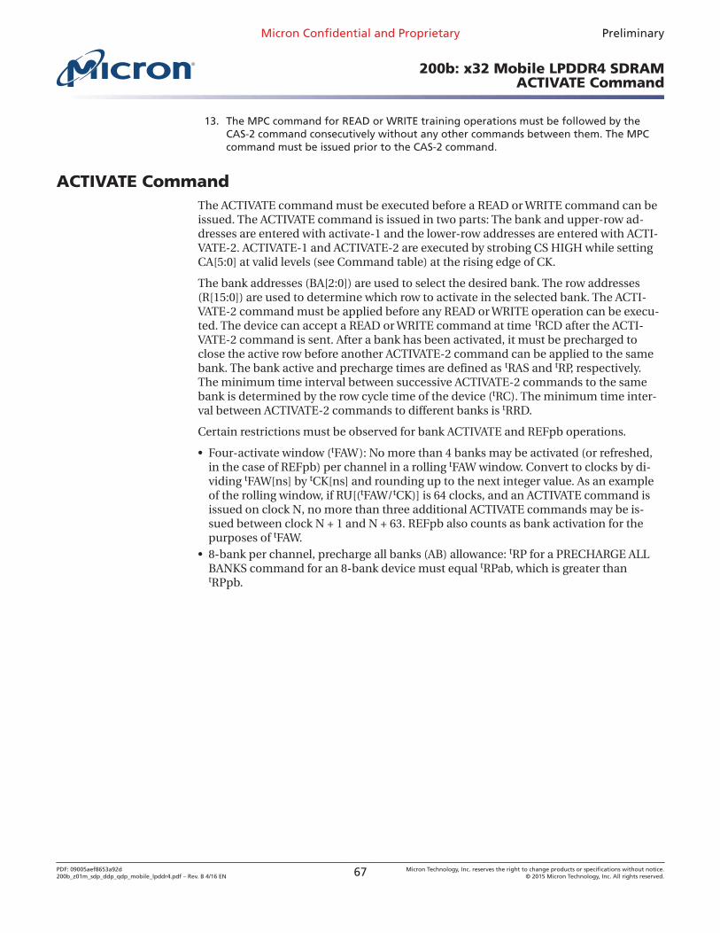
13. The MPC command for READ or WRITE training operations must be followed by theCAS-2 command consecutively without any other commands between them. The MPCcommand must be issued prior to the CAS-2 command.
ACTIVATE CommandThe ACTIVATE command must be executed before a READ or WRITE command can beissued. The ACTIVATE command is issued in two parts: The bank and upper-row ad-dresses are entered with activate-1 and the lower-row addresses are entered with ACTI-VATE-2. ACTIVATE-1 and ACTIVATE-2 are executed by strobing CS HIGH while settingCA[5:0] at valid levels (see Command table) at the rising edge of CK.
The bank addresses (BA[2:0]) are used to select the desired bank. The row addresses(R[15:0]) are used to determine which row to activate in the selected bank. The ACTI-VATE-2 command must be applied before any READ or WRITE operation can be execu-ted. The device can accept a READ or WRITE command at time tRCD after the ACTI-VATE-2 command is sent. After a bank has been activated, it must be precharged toclose the active row before another ACTIVATE-2 command can be applied to the samebank. The bank active and precharge times are defined as tRAS and tRP, respectively.The minimum time interval between successive ACTIVATE-2 commands to the samebank is determined by the row cycle time of the device (tRC). The minimum time inter-val between ACTIVATE-2 commands to different banks is tRRD.
Certain restrictions must be observed for bank ACTIVATE and REFpb operations.
• Four-activate window (tFAW): No more than 4 banks may be activated (or refreshed,in the case of REFpb) per channel in a rolling tFAW window. Convert to clocks by di-viding tFAW[ns] by tCK[ns] and rounding up to the next integer value. As an exampleof the rolling window, if RU[(tFAW/tCK)] is 64 clocks, and an ACTIVATE command isissued on clock N, no more than three additional ACTIVATE commands may be is-sued between clock N + 1 and N + 63. REFpb also counts as bank activation for thepurposes of tFAW.
• 8-bank per channel, precharge all banks (AB) allowance: tRP for a PRECHARGE ALLBANKS command for an 8-bank device must equal tRPab, which is greater thantRPpb.
Micron Confidential and Proprietary Preliminary
200b: x32 Mobile LPDDR4 SDRAMACTIVATE Command
PDF: 09005aef8653a92d200b_z01m_sdp_ddp_qdp_mobile_lpddr4.pdf – Rev. B 4/16 EN 67 Micron Technology, Inc. reserves the right to change products or specifications without notice.
© 2015 Micron Technology, Inc. All rights reserved.
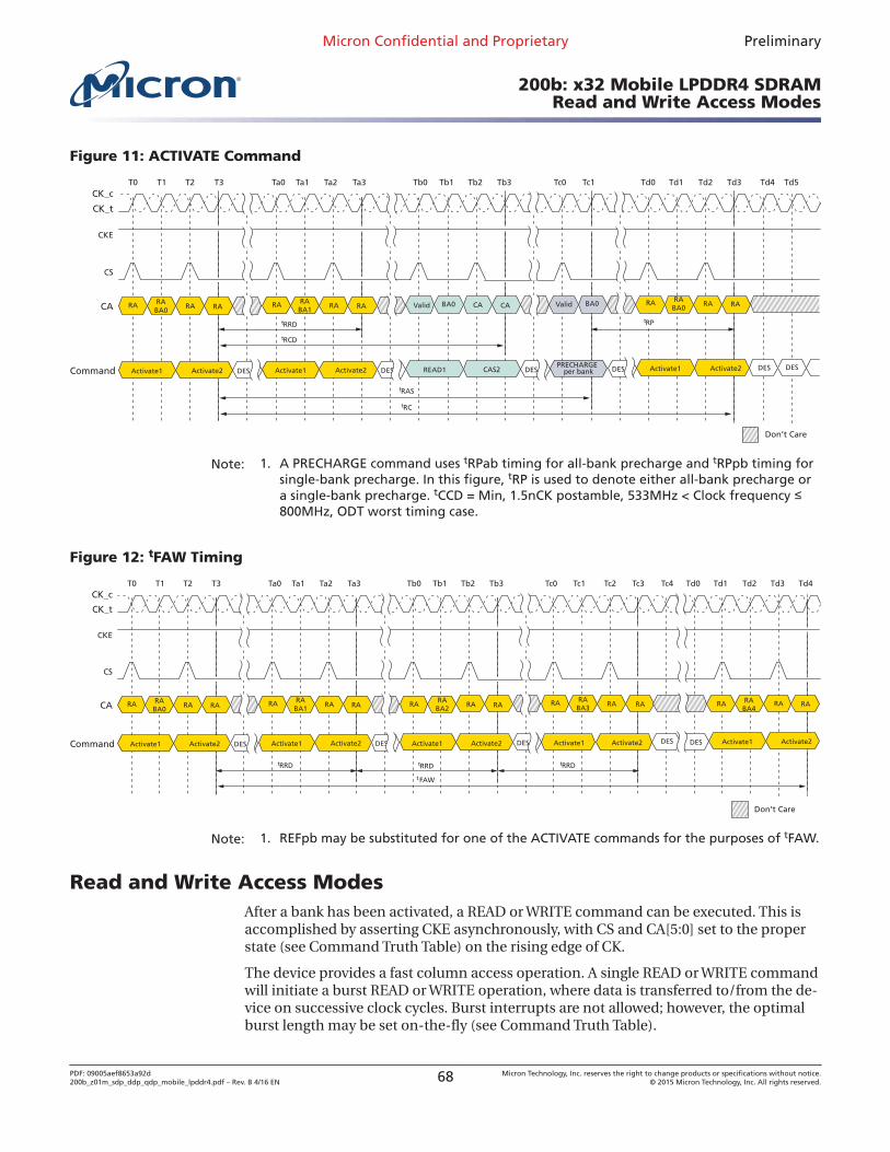
Figure 11: ACTIVATE Command
T0 T1 T2 T3 Td0 Td1 Td3Td2CK_c
CK_t
Ta1Ta0 Ta3Ta2 Td5Td4Tb1Tb0 Tb3 Tc1Tb2 Tc0
CA
Command
tRRD
tRCD
tRP
tRAS
tRC
RA RA RA
DESActivate1 Activate2
RABA0
RA RA RA
Activate1 Activate2
RABA1
DES
RA RA RA
Activate1 Activate2
RABA0CA CA
READ1 CAS2
BA0
DES DES
Valid
CS
CKE
Don’t Care
DESPRECHARGE
BA0Valid
DES per bank
Note: 1. A PRECHARGE command uses tRPab timing for all-bank precharge and tRPpb timing forsingle-bank precharge. In this figure, tRP is used to denote either all-bank precharge ora single-bank precharge. tCCD = Min, 1.5nCK postamble, 533MHz < Clock frequency ≤800MHz, ODT worst timing case.
Figure 12: tFAW Timing
T0 T1 T2 T3 Td0 Td1 Td3Td2CK_c
CK_t
Ta1Ta0 Ta3Ta2 Td4Tb1Tb0 Tb3 Tc1Tb2 Tc0 Tc3 Tc4Tc2
CA
Command
tRRD
tFAW
RA RA RA
DESActivate1 Activate2
RABA0
RA RA RA
Activate1 Activate2
RABA1
RA RA RA
Activate1 Activate2
RABA3
DESDES
RA RA RA
Activate1 Activate2
RABA4
CS
CKE
Don’t Care
tRRD tRRD
DES DES
RABA2 RA RA
Activate1 Activate2
RA
Note: 1. REFpb may be substituted for one of the ACTIVATE commands for the purposes of tFAW.
Read and Write Access ModesAfter a bank has been activated, a READ or WRITE command can be executed. This isaccomplished by asserting CKE asynchronously, with CS and CA[5:0] set to the properstate (see Command Truth Table) on the rising edge of CK.
The device provides a fast column access operation. A single READ or WRITE commandwill initiate a burst READ or WRITE operation, where data is transferred to/from the de-vice on successive clock cycles. Burst interrupts are not allowed; however, the optimalburst length may be set on-the-fly (see Command Truth Table).
Micron Confidential and Proprietary Preliminary
200b: x32 Mobile LPDDR4 SDRAMRead and Write Access Modes
PDF: 09005aef8653a92d200b_z01m_sdp_ddp_qdp_mobile_lpddr4.pdf – Rev. B 4/16 EN 68 Micron Technology, Inc. reserves the right to change products or specifications without notice.
© 2015 Micron Technology, Inc. All rights reserved.
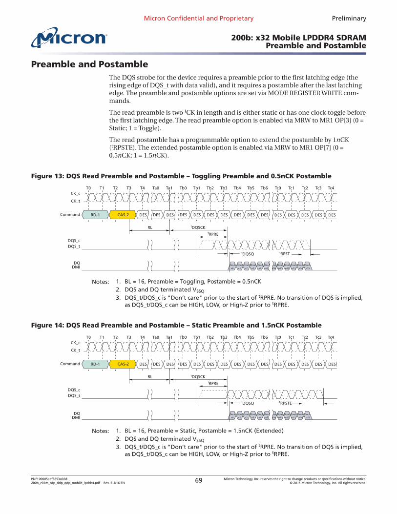
Preamble and PostambleThe DQS strobe for the device requires a preamble prior to the first latching edge (therising edge of DQS_t with data valid), and it requires a postamble after the last latchingedge. The preamble and postamble options are set via MODE REGISTER WRITE com-mands.
The read preamble is two tCK in length and is either static or has one clock toggle beforethe first latching edge. The read preamble option is enabled via MRW to MR1 OP[3] (0 =Static; 1 = Toggle).
The read postamble has a programmable option to extend the postamble by 1nCK(tRPSTE). The extended postamble option is enabled via MRW to MR1 OP[7] (0 =0.5nCK; 1 = 1.5nCK).
Figure 13: DQS Read Preamble and Postamble – Toggling Preamble and 0.5nCK Postamble
T0
CK_t
CK_cT1 T2 T3 T4 Ta0 Tc3Ta1 Tb4Tb0 Tb1 Tb2 Tb3 Tb6 Tc4Tc0 Tc1 Tc2Tb5
RD-1Command DES DES DES DES DESDES DES DES DES DES DES DESDES DES DES
tRPST
tRPRE
tDQSQ
tDQSCK
DQS_tDQS_c
RL
DMIDQ
Doutn0
Doutn15
Doutn14
Doutn13
Doutn12
Doutn11
Doutn10
Doutn5
Doutn4
Doutn3
Doutn2
Doutn1
CAS-2
Notes: 1. BL = 16, Preamble = Toggling, Postamble = 0.5nCK2. DQS and DQ terminated VSSQ
3. DQS_t/DQS_c is "Don’t care" prior to the start of tRPRE. No transition of DQS is implied,as DQS_t/DQS_c can be HIGH, LOW, or High-Z prior to tRPRE.
Figure 14: DQS Read Preamble and Postamble – Static Preamble and 1.5nCK Postamble
T0
CK_t
CK_cT1 T2 T3 T4 Ta0 Tc3Ta1 Tb4Tb0 Tb1 Tb2 Tb3 Tb6 Tc4Tc0 Tc1 Tc2Tb5
Command DES DES DES DES DESDES DES DES DES DES DES DESDES DES DES
tRPSTE
tRPRE
tDQSQ
tDQSCK
DQS_tDQS_c
RL
Doutn0
Doutn15
Doutn14
Doutn13
Doutn12
Doutn11
Doutn10
Doutn5
Doutn4
Doutn3
Doutn2
Doutn1DMI
DQ
RD-1 CAS-2
Notes: 1. BL = 16, Preamble = Static, Postamble = 1.5nCK (Extended)2. DQS and DQ terminated VSSQ
3. DQS_t/DQS_c is "Don’t care" prior to the start of tRPRE. No transition of DQS is implied,as DQS_t/DQS_c can be HIGH, LOW, or High-Z prior to tRPRE.
Micron Confidential and Proprietary Preliminary
200b: x32 Mobile LPDDR4 SDRAMPreamble and Postamble
PDF: 09005aef8653a92d200b_z01m_sdp_ddp_qdp_mobile_lpddr4.pdf – Rev. B 4/16 EN 69 Micron Technology, Inc. reserves the right to change products or specifications without notice.
© 2015 Micron Technology, Inc. All rights reserved.
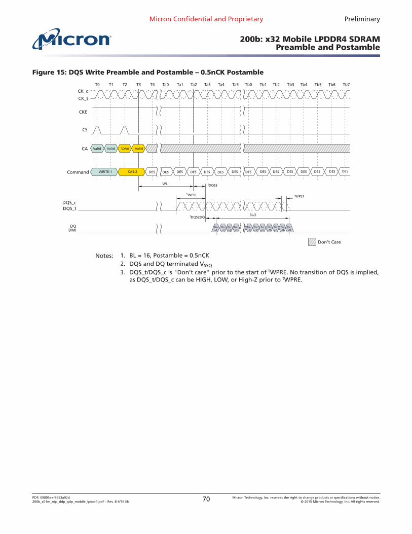
Figure 15: DQS Write Preamble and Postamble – 0.5nCK Postamble
T0 T1 T2 T3 T4 Ta0 Ta1 Ta3 Ta5Ta2 Ta4 Tb0 Tb2 Tb4Tb1 Tb3 Tb5 Tb6
CK_c
CK_t
Tb7
CA
CS
CKE
Command
WL
Valid Valid Valid Valid
CAS-2WRITE-1 DESDES DESDES DESDES DESDES
DQS_cDQS_t
Don’t Care
tWPST
tDQS2DQ
DESDES DES DESDESDES DES
tDQSS
tWPRE
Dinn0
Dinn1
Dinn2
Dinn3
Dinn8
Dinn9
Dinn14
Dinn15
Dinn13
Dinn12
BL/2
Dinn11
Dinn10DMI
DQ
Notes: 1. BL = 16, Postamble = 0.5nCK2. DQS and DQ terminated VSSQ
3. DQS_t/DQS_c is "Don’t care" prior to the start of tWPRE. No transition of DQS is implied,as DQS_t/DQS_c can be HIGH, LOW, or High-Z prior to tWPRE.
Micron Confidential and Proprietary Preliminary
200b: x32 Mobile LPDDR4 SDRAMPreamble and Postamble
PDF: 09005aef8653a92d200b_z01m_sdp_ddp_qdp_mobile_lpddr4.pdf – Rev. B 4/16 EN 70 Micron Technology, Inc. reserves the right to change products or specifications without notice.
© 2015 Micron Technology, Inc. All rights reserved.
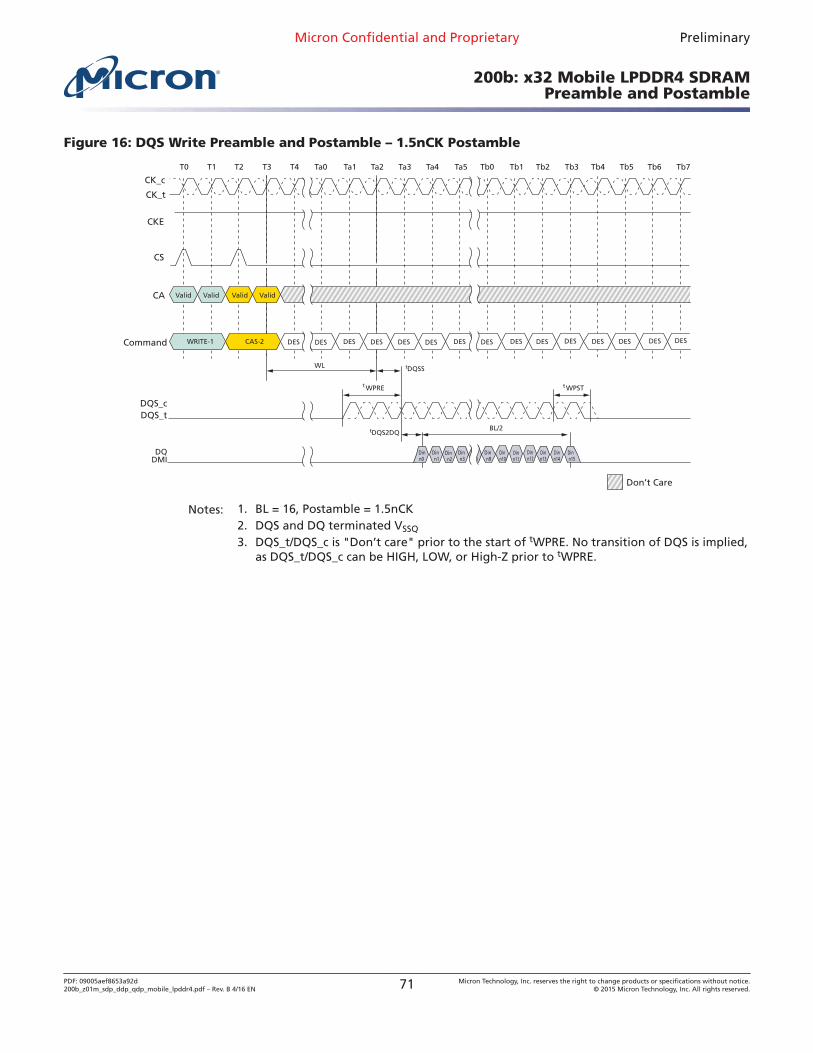
Figure 16: DQS Write Preamble and Postamble – 1.5nCK Postamble
T0 T1 T2 T3 T4 Ta0 Ta1 Ta3 Ta5Ta2 Ta4 Tb0 Tb2 Tb4Tb1 Tb3 Tb5 Tb6
CK_c
CK_t
Tb7
CA
CS
CKE
Command
WL
Valid Valid Valid Valid
CAS-2WRITE-1 DESDES DESDES DESDES DESDES
DQS_cDQS_t
Don’t Care
tWPST
tDQS2DQ
DESDES DES DESDESDES DES
tDQSS
tWPRE
Dinn0
Dinn1
Dinn2
Dinn3
Dinn8
Dinn9
Dinn14
Dinn15
Dinn13
Dinn12
BL/2
Dinn11
Dinn10DMI
DQ
Notes: 1. BL = 16, Postamble = 1.5nCK2. DQS and DQ terminated VSSQ
3. DQS_t/DQS_c is "Don’t care" prior to the start of tWPRE. No transition of DQS is implied,as DQS_t/DQS_c can be HIGH, LOW, or High-Z prior to tWPRE.
Micron Confidential and Proprietary Preliminary
200b: x32 Mobile LPDDR4 SDRAMPreamble and Postamble
PDF: 09005aef8653a92d200b_z01m_sdp_ddp_qdp_mobile_lpddr4.pdf – Rev. B 4/16 EN 71 Micron Technology, Inc. reserves the right to change products or specifications without notice.
© 2015 Micron Technology, Inc. All rights reserved.
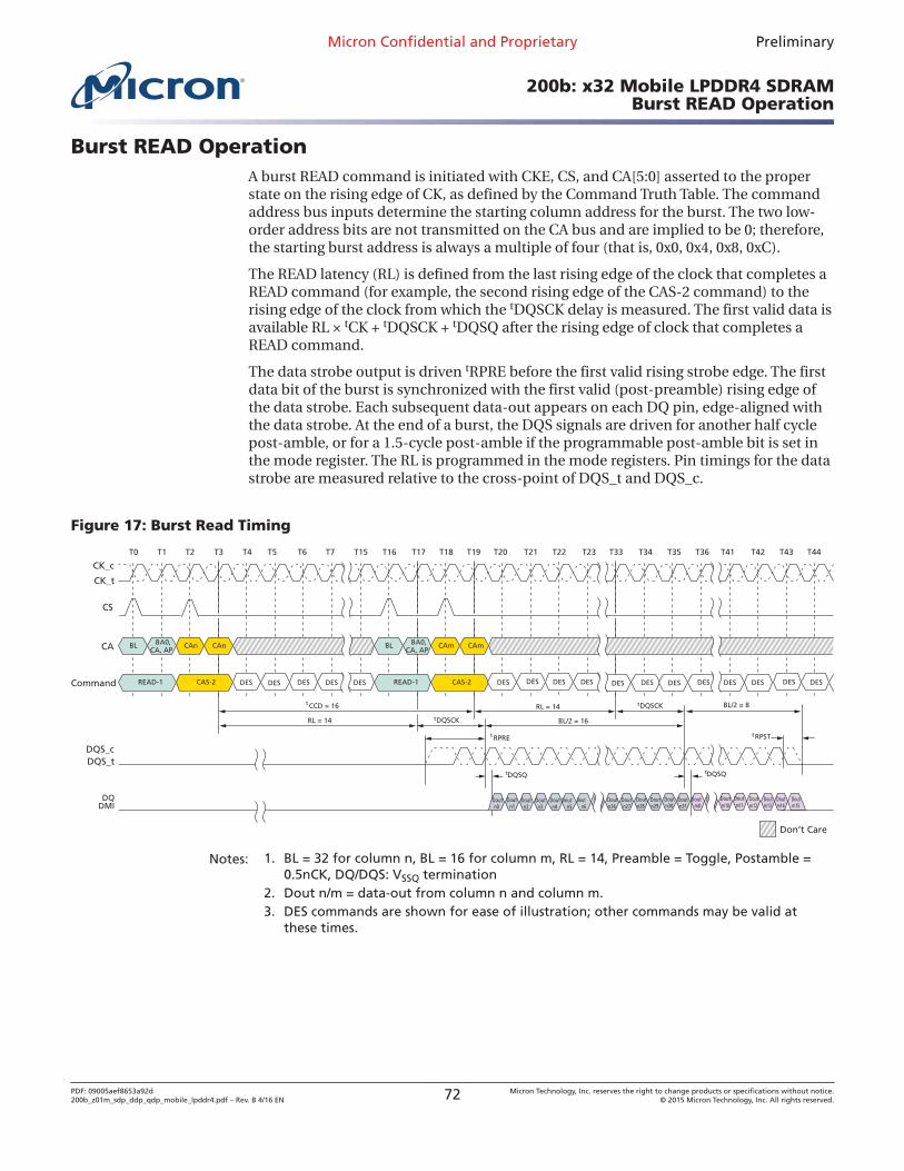
Burst READ OperationA burst READ command is initiated with CKE, CS, and CA[5:0] asserted to the properstate on the rising edge of CK, as defined by the Command Truth Table. The commandaddress bus inputs determine the starting column address for the burst. The two low-order address bits are not transmitted on the CA bus and are implied to be 0; therefore,the starting burst address is always a multiple of four (that is, 0x0, 0x4, 0x8, 0xC).
The READ latency (RL) is defined from the last rising edge of the clock that completes aREAD command (for example, the second rising edge of the CAS-2 command) to therising edge of the clock from which the tDQSCK delay is measured. The first valid data isavailable RL × tCK + tDQSCK + tDQSQ after the rising edge of clock that completes aREAD command.
The data strobe output is driven tRPRE before the first valid rising strobe edge. The firstdata bit of the burst is synchronized with the first valid (post-preamble) rising edge ofthe data strobe. Each subsequent data-out appears on each DQ pin, edge-aligned withthe data strobe. At the end of a burst, the DQS signals are driven for another half cyclepost-amble, or for a 1.5-cycle post-amble if the programmable post-amble bit is set inthe mode register. The RL is programmed in the mode registers. Pin timings for the datastrobe are measured relative to the cross-point of DQS_t and DQS_c.
Figure 17: Burst Read Timing
T0 T1 T2 T3 T4 T5 T6 T15 T17T7 T16 T18 T19 T20 T22 T33T21 T23 T34 T35
CK_c
CK_t
T36 T41 T43T42 T44
CA
CS
Command
CAnCAnBA0,CA, AP
BL
CAS-2READ-1
CAmCAmBA0,CA, AP
BL
CAS-2READ-1DESDES DESDES DES
DQS_cDQS_t
Don’t Care
t
tRPST
tDQSQ tDQSQ
DQSCK
tDQSCK
DES DESDES DES DES DES DES DESDESDES DES DES
RL = 14
RL = 14 BL/2 = 8
BL/2 = 16
tRPRE
tCCD = 16
Doutn0
Doutn1
Doutn2
Doutn3
Doutn4
Doutn5
Doutn7
Doutn6
Doutn27
Doutn26
Doutn28
Doutn29
Doutn30
Doutn31
Doutm0
Doutm1
Doutm11
Doutm10
Doutm14
Doutm15
Doutm13
Doutm12DMI
DQ
Notes: 1. BL = 32 for column n, BL = 16 for column m, RL = 14, Preamble = Toggle, Postamble =0.5nCK, DQ/DQS: VSSQ termination
2. Dout n/m = data-out from column n and column m.3. DES commands are shown for ease of illustration; other commands may be valid at
these times.
Micron Confidential and Proprietary Preliminary
200b: x32 Mobile LPDDR4 SDRAMBurst READ Operation
PDF: 09005aef8653a92d200b_z01m_sdp_ddp_qdp_mobile_lpddr4.pdf – Rev. B 4/16 EN 72 Micron Technology, Inc. reserves the right to change products or specifications without notice.
© 2015 Micron Technology, Inc. All rights reserved.
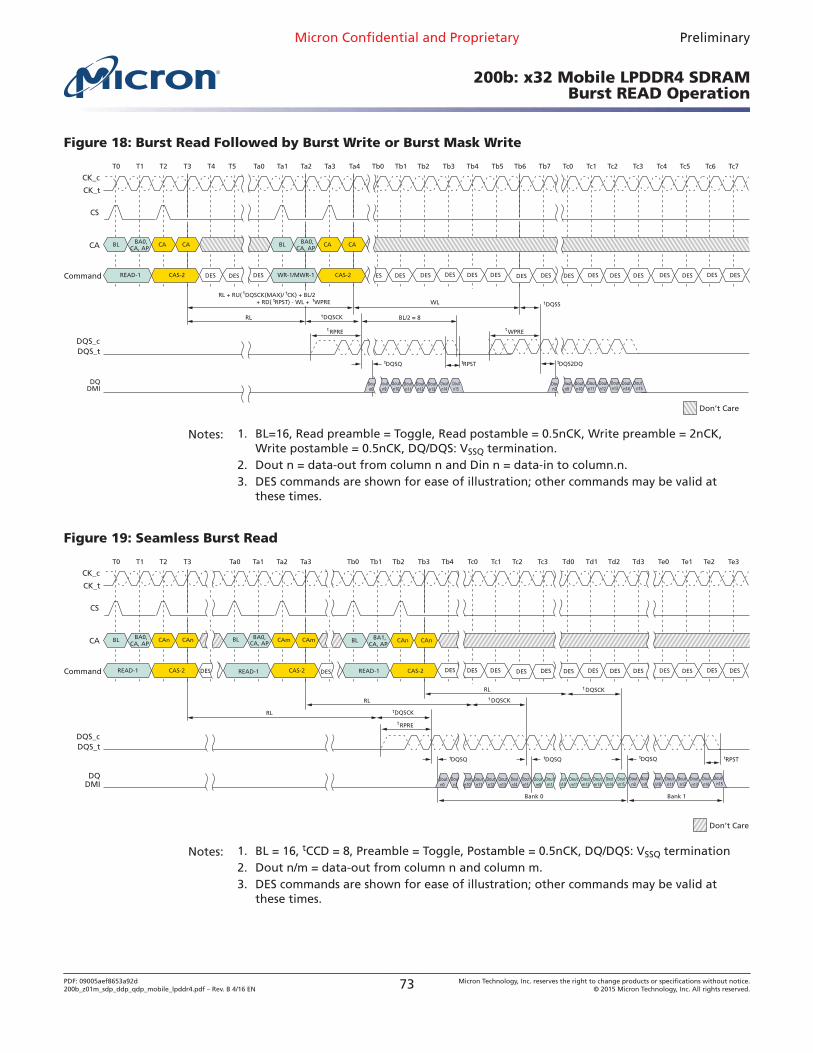
Figure 18: Burst Read Followed by Burst Write or Burst Mask Write
T0 T1 T2 T3 T4 T5 Ta0 Ta2 Ta4Ta1 Ta3 Tb0 Tb1 Tb2 Tb4 Tb6Tb3 Tb5 Tb7 Tc0
CK_c
CK_t
Tc1 Tc2 Tc4Tc3 Tc5 Tc6 Tc7
CA
CS
Command
CACABA0,CA, AP
BL
CAS-2READ-1
CACABA0,CA, AP
BL
CAS-2WR-1/MWR-1DESDES DESDES DES
DQS_cDQS_t
Don’t Care
t
tDQSQ tDQS2DQ
DQSS
t
t t
tt
DQSCK
DES DESDES DES DES DES DES DESDES DESDESDES DES DES
RL
WL
BL/2 = 8
tRPRE tWPRE
RL + RU( DQSCK(MAX)/ CK) + BL/2 + RD( RPST) - WL + WPRE
Dout Doutn0 n0
Doutn9
Doutn10
Doutn11
Doutn12
Doutn13
Doutn15
Doutn14
Doutn10
Doutn9
Doutn11
Doutn12
Doutn13
Doutn14
Doutn15
tRPST
DMIDQ
Notes: 1. BL=16, Read preamble = Toggle, Read postamble = 0.5nCK, Write preamble = 2nCK,Write postamble = 0.5nCK, DQ/DQS: VSSQ termination.
2. Dout n = data-out from column n and Din n = data-in to column.n.3. DES commands are shown for ease of illustration; other commands may be valid at
these times.
Figure 19: Seamless Burst Read
T0 T1 T2 T3 Ta0 Ta2Ta1 Ta3 Tb0 Tb1 Tb2 Tb4Tb3 Tc0
CK_c
CK_t
Tc1 Tc2 Tc3 Td0 Td1 Td2 Td3 Te0 Te1 Te2 Te3
CA
CS
Command
CAnCAnBA0,CA, AP
BL
CAS-2READ-1
CAnCAnBA1,CA, AP
BL
CAS-2READ-1
CA, APBL
READ-1
CAmCAm
CAS-2DES DES
DQS_cDQS_t
DQDMI
Don’t Care
tDQSQ
t
t
DQSCK
DESDES DES DES DES DES DESDES DESDESDES DES DES
RL
RL
tRPRE
Doutn0
Doutn1
Doutn10
Doutn11
Doutn12
Doutn13
Doutn15
Doutn14
Doutm0
Doutm1
Doutm10
Doutm11
Doutm12
Doutm13
Doutm15
Doutm14
Doutn15
Dout Dout Dout Dout Dout Dout Dout
tRPSTtDQSQ
Bank 0 Bank 1
tDQSQ
DQSCKRL
t DQSCK
BA0,
n0 n1 n10 n11 n12 n13 n14
Notes: 1. BL = 16, tCCD = 8, Preamble = Toggle, Postamble = 0.5nCK, DQ/DQS: VSSQ termination2. Dout n/m = data-out from column n and column m.3. DES commands are shown for ease of illustration; other commands may be valid at
these times.
Micron Confidential and Proprietary Preliminary
200b: x32 Mobile LPDDR4 SDRAMBurst READ Operation
PDF: 09005aef8653a92d200b_z01m_sdp_ddp_qdp_mobile_lpddr4.pdf – Rev. B 4/16 EN 73 Micron Technology, Inc. reserves the right to change products or specifications without notice.
© 2015 Micron Technology, Inc. All rights reserved.
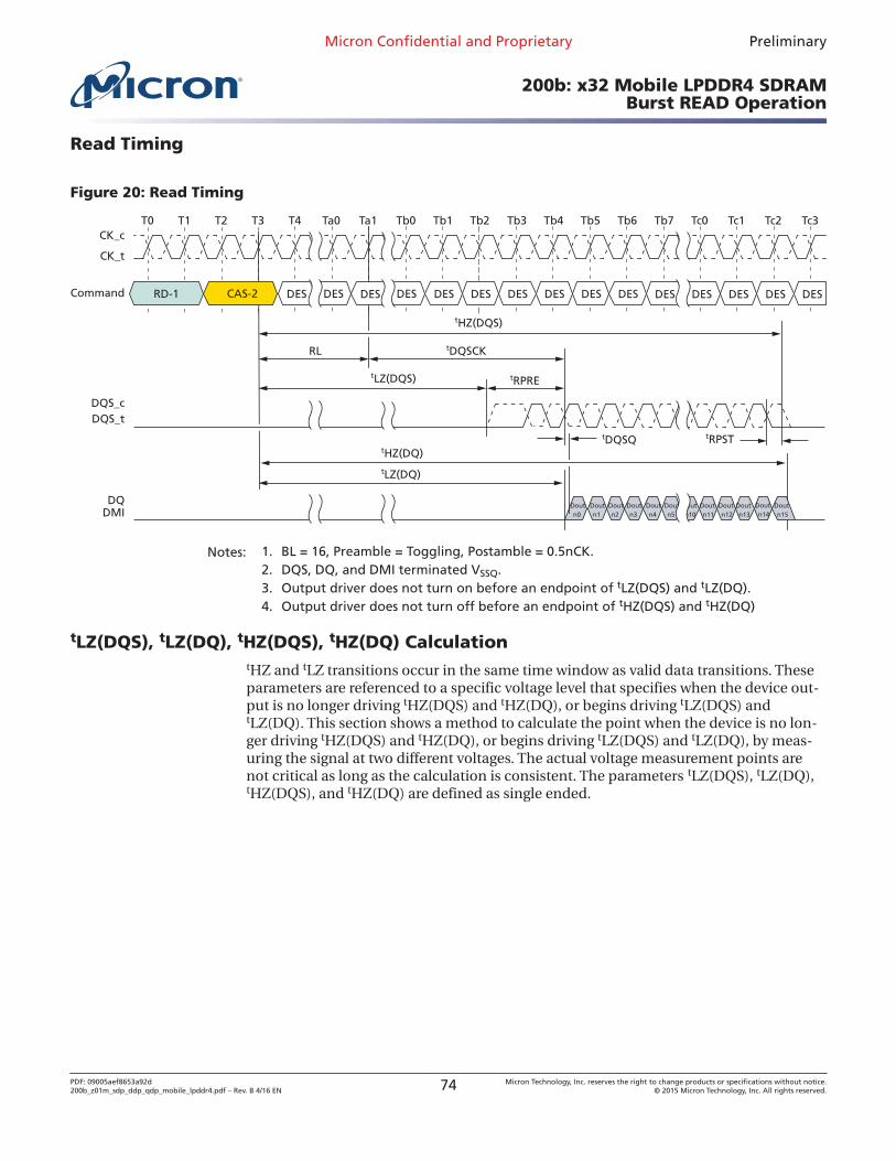
Read Timing
Figure 20: Read Timing
T0
CK_t
CK_cT1 T2 T3 T4 Ta0 Tc3Ta1 Tb4Tb0 Tb1 Tb2 Tb3 Tb6 Tb7 Tc0 Tc1 Tc2Tb5
Command DES DES DES DES DESDES DES DES DES DES DES DESDES DES DES
tRPST
tRPRE
tDQSQ
tDQSCK
tHZ(DQ)tLZ(DQ)
tHZ(DQS)
tLZ(DQS)
DQS_tDQS_c
RL
DMIDQ Dout
n0Doutn15
Doutn14
Doutn13
Doutn12
Doutn11
Doutn10
Doutn5
Doutn4
Doutn3
Doutn2
Doutn1
RD-1 CAS-2
Notes: 1. BL = 16, Preamble = Toggling, Postamble = 0.5nCK.2. DQS, DQ, and DMI terminated VSSQ.3. Output driver does not turn on before an endpoint of tLZ(DQS) and tLZ(DQ).4. Output driver does not turn off before an endpoint of tHZ(DQS) and tHZ(DQ)
tLZ(DQS), tLZ(DQ), tHZ(DQS), tHZ(DQ) CalculationtHZ and tLZ transitions occur in the same time window as valid data transitions. Theseparameters are referenced to a specific voltage level that specifies when the device out-put is no longer driving tHZ(DQS) and tHZ(DQ), or begins driving tLZ(DQS) andtLZ(DQ). This section shows a method to calculate the point when the device is no lon-ger driving tHZ(DQS) and tHZ(DQ), or begins driving tLZ(DQS) and tLZ(DQ), by meas-uring the signal at two different voltages. The actual voltage measurement points arenot critical as long as the calculation is consistent. The parameters tLZ(DQS), tLZ(DQ),tHZ(DQS), and tHZ(DQ) are defined as single ended.
Micron Confidential and Proprietary Preliminary
200b: x32 Mobile LPDDR4 SDRAMBurst READ Operation
PDF: 09005aef8653a92d200b_z01m_sdp_ddp_qdp_mobile_lpddr4.pdf – Rev. B 4/16 EN 74 Micron Technology, Inc. reserves the right to change products or specifications without notice.
© 2015 Micron Technology, Inc. All rights reserved.
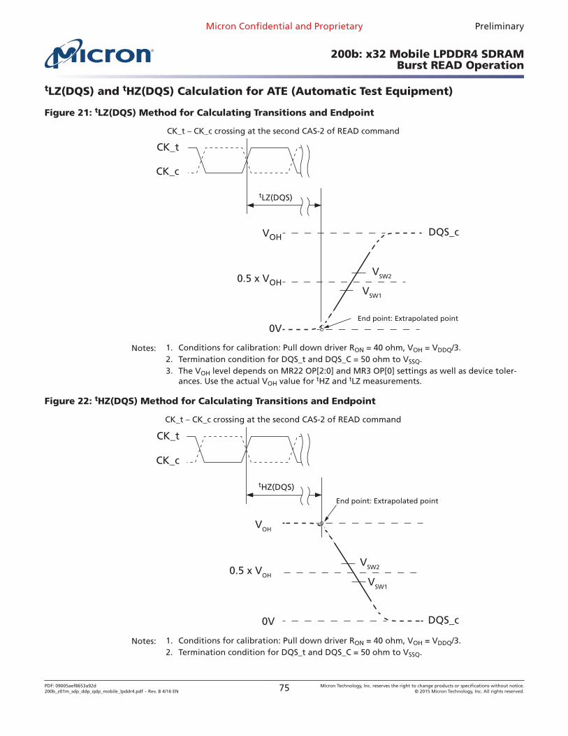
tLZ(DQS) and tHZ(DQS) Calculation for ATE (Automatic Test Equipment)
Figure 21: tLZ(DQS) Method for Calculating Transitions and Endpoint
CK_c
DQS_cVOH
VSW2
VSW1
End point: Extrapolated point
CK_t – CK_c crossing at the second CAS-2 of READ command
0V
0.5 x VOH
CK_t
tLZ(DQS)
Notes: 1. Conditions for calibration: Pull down driver RON = 40 ohm, VOH = VDDQ/3.2. Termination condition for DQS_t and DQS_C = 50 ohm to VSSQ.3. The VOH level depends on MR22 OP[2:0] and MR3 OP[0] settings as well as device toler-
ances. Use the actual VOH value for tHZ and tLZ measurements.
Figure 22: tHZ(DQS) Method for Calculating Transitions and Endpoint
CK_c
DQS_c
VSW2
VSW1
End point: Extrapolated point
CK_t – CK_c crossing at the second CAS-2 of READ command
CK_t
tHZ(DQS)
VOH
0V
0.5 x VOH
Notes: 1. Conditions for calibration: Pull down driver RON = 40 ohm, VOH = VDDQ/3.2. Termination condition for DQS_t and DQS_C = 50 ohm to VSSQ.
Micron Confidential and Proprietary Preliminary
200b: x32 Mobile LPDDR4 SDRAMBurst READ Operation
PDF: 09005aef8653a92d200b_z01m_sdp_ddp_qdp_mobile_lpddr4.pdf – Rev. B 4/16 EN 75 Micron Technology, Inc. reserves the right to change products or specifications without notice.
© 2015 Micron Technology, Inc. All rights reserved.
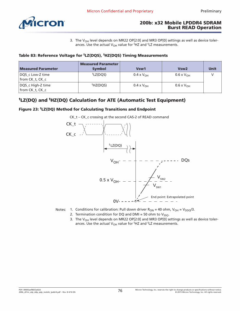
3. The VOH level depends on MR22 OP[2:0] and MR3 OP[0] settings as well as device toler-ances. Use the actual VOH value for tHZ and tLZ measurements.
Table 83: Reference Voltage for tLZ(DQS), tHZ(DQS) Timing Measurements
Measured ParameterMeasured Parameter
Symbol Vsw1 Vsw2 Unit
DQS_c Low-Z timefrom CK_t, CK_c
tLZ(DQS) 0.4 x VOH 0.6 x VOH V
DQS_c High-Z timefrom CK_t, CK_c
tHZ(DQS) 0.4 x VOH 0.6 x VOH
tLZ(DQ) and tHZ(DQ) Calculation for ATE (Automatic Test Equipment)
Figure 23: tLZ(DQ) Method for Calculating Transitions and Endpoint
CK_c
DQsVOH
VSW2
VSW1
End point: Extrapolated point
CK_t – CK_c crossing at the second CAS-2 of READ command
0V
0.5 x VOH
CK_t
t LZ(DQ)
Notes: 1. Conditions for calibration: Pull down driver RON = 40 ohm, VOH = VDDQ/3.2. Termination condition for DQ and DMI = 50 ohm to VSSQ.3. The VOH level depends on MR22 OP[2:0] and MR3 OP[0] settings as well as device toler-
ances. Use the actual VOH value for tHZ and tLZ measurements.
Micron Confidential and Proprietary Preliminary
200b: x32 Mobile LPDDR4 SDRAMBurst READ Operation
PDF: 09005aef8653a92d200b_z01m_sdp_ddp_qdp_mobile_lpddr4.pdf – Rev. B 4/16 EN 76 Micron Technology, Inc. reserves the right to change products or specifications without notice.
© 2015 Micron Technology, Inc. All rights reserved.
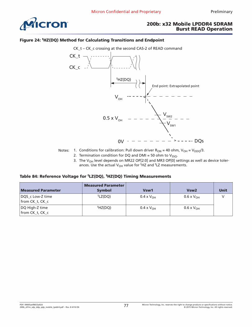
Figure 24: tHZ(DQ) Method for Calculating Transitions and Endpoint
CK_c
DQs
VSW2
VSW1
End point: Extrapolated point
CK_t – CK_c crossing at the second CAS-2 of READ command
CK_t
tHZ(DQ)
VOH
0V
0.5 x VOH
Notes: 1. Conditions for calibration: Pull down driver RON = 40 ohm, VOH = VDDQ/3.2. Termination condition for DQ and DMI = 50 ohm to VSSQ.3. The VOH level depends on MR22 OP[2:0] and MR3 OP[0] settings as well as device toler-
ances. Use the actual VOH value for tHZ and tLZ measurements.
Table 84: Reference Voltage for tLZ(DQ), tHZ(DQ) Timing Measurements
Measured ParameterMeasured Parameter
Symbol Vsw1 Vsw2 Unit
DQS_c Low-Z timefrom CK_t, CK_c
tLZ(DQ) 0.4 x VOH 0.6 x VOH V
DQ High-Z timefrom CK_t, CK_c
tHZ(DQ) 0.4 x VOH 0.6 x VOH
Micron Confidential and Proprietary Preliminary
200b: x32 Mobile LPDDR4 SDRAMBurst READ Operation
PDF: 09005aef8653a92d200b_z01m_sdp_ddp_qdp_mobile_lpddr4.pdf – Rev. B 4/16 EN 77 Micron Technology, Inc. reserves the right to change products or specifications without notice.
© 2015 Micron Technology, Inc. All rights reserved.
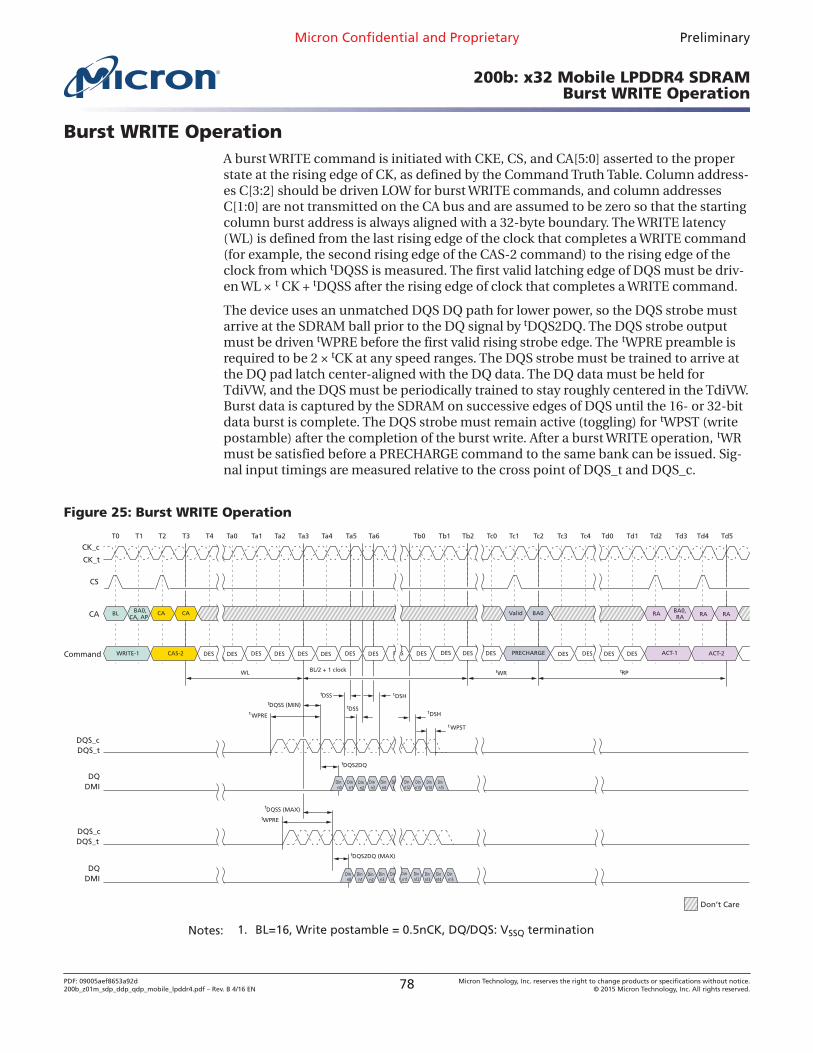
Burst WRITE OperationA burst WRITE command is initiated with CKE, CS, and CA[5:0] asserted to the properstate at the rising edge of CK, as defined by the Command Truth Table. Column address-es C[3:2] should be driven LOW for burst WRITE commands, and column addressesC[1:0] are not transmitted on the CA bus and are assumed to be zero so that the startingcolumn burst address is always aligned with a 32-byte boundary. The WRITE latency(WL) is defined from the last rising edge of the clock that completes a WRITE command(for example, the second rising edge of the CAS-2 command) to the rising edge of theclock from which tDQSS is measured. The first valid latching edge of DQS must be driv-en WL × t CK + tDQSS after the rising edge of clock that completes a WRITE command.
The device uses an unmatched DQS DQ path for lower power, so the DQS strobe mustarrive at the SDRAM ball prior to the DQ signal by tDQS2DQ. The DQS strobe outputmust be driven tWPRE before the first valid rising strobe edge. The tWPRE preamble isrequired to be 2 × tCK at any speed ranges. The DQS strobe must be trained to arrive atthe DQ pad latch center-aligned with the DQ data. The DQ data must be held forTdiVW, and the DQS must be periodically trained to stay roughly centered in the TdiVW.Burst data is captured by the SDRAM on successive edges of DQS until the 16- or 32-bitdata burst is complete. The DQS strobe must remain active (toggling) for tWPST (writepostamble) after the completion of the burst write. After a burst WRITE operation, tWRmust be satisfied before a PRECHARGE command to the same bank can be issued. Sig-nal input timings are measured relative to the cross point of DQS_t and DQS_c.
Figure 25: Burst WRITE Operation
T0 T1 T2 T3 T4 Ta0 Ta1 Ta3 Ta5Ta2 Ta4 Ta6 Tb0 Tb2 Tc1Tb1 Tc0 Tc2 Tc3
CK_c
CK_t
Tc4 Td0 Td2Td1 Td4Td3 Td5
CA
CS
Command
WL
CACABA0,CA, AP
BL BA0,RA
CAS-2WRITE-1 DESDES DESDES DESDES DESDES PRECHARGE
Valid BA0
ACT-1
RARA RA
ACT-2
DQS_cDQS_t
DMIDQ
DMIDQ
Don’t Care
tRPtWR
tWPST
tDQS2DQ
DQS_cDQS_t
tWPRE
tDQSS (MAX)
tDQS2DQ (MAX)
DESDES DESDES DES DESDES DES DES
BL/2 + 1 clock
tDSS
tDSS
tDSH
tDSH
tDQSS (MIN)tWPRE
Dinn0
Dinn1
Dinn2
Dinn3
Dinn4
Dinn5
Dinn14
Dinn15
Dinn13
Dinn12
Dinn0
Dinn1
Dinn2
Dinn3
Dinn4
Dinn11
Dinn14
Dinn15
Dinn13
Dinn12
Notes: 1. BL=16, Write postamble = 0.5nCK, DQ/DQS: VSSQ termination
Micron Confidential and Proprietary Preliminary
200b: x32 Mobile LPDDR4 SDRAMBurst WRITE Operation
PDF: 09005aef8653a92d200b_z01m_sdp_ddp_qdp_mobile_lpddr4.pdf – Rev. B 4/16 EN 78 Micron Technology, Inc. reserves the right to change products or specifications without notice.
© 2015 Micron Technology, Inc. All rights reserved.
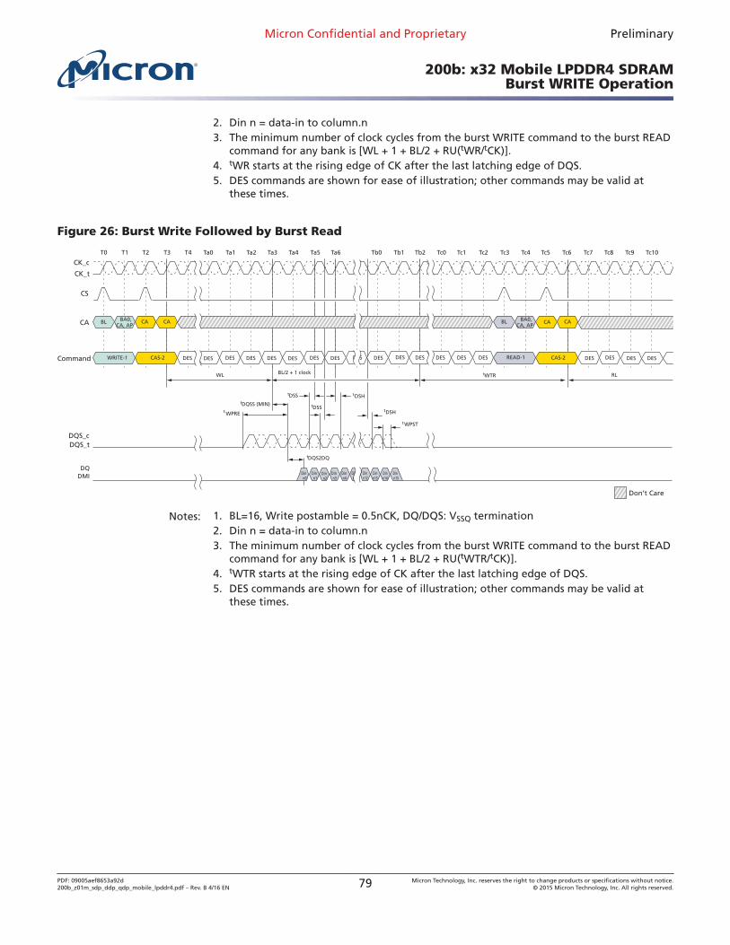
2. Din n = data-in to column.n3. The minimum number of clock cycles from the burst WRITE command to the burst READ
command for any bank is [WL + 1 + BL/2 + RU(tWR/tCK)].4. tWR starts at the rising edge of CK after the last latching edge of DQS.5. DES commands are shown for ease of illustration; other commands may be valid at
these times.
Figure 26: Burst Write Followed by Burst Read
T0 T1 T2 T3 T4 Ta0 Ta1 Ta3 Ta5Ta2 Ta4 Ta6 Tb0 Tb2 Tc1Tb1 Tc0 Tc2 Tc3
CK_c
CK_t
Tc4 Tc6Tc5 Tc7 Tc8 Tc9 Tc10
CA
CS
Command
WL
CACABA0,CA, AP
BL
CAS-2
CACA
CAS-2WRITE-1 DESDES DESDES DESDES DESDES READ-1
BL
DQS_cDQS_t
Don’t Care
RLtWTR
tWPST
tDQS2DQ
DESDES DESDES DES DES DES DESDES DES DES
BL/2 + 1 clock
tDSS
tDSS
tDSH
tDSH
tDQSS (MIN)tWPRE
Dinn0
Dinn1
Dinn2
Dinn3
Dinn4
Dinn5
Dinn14
Dinn15
Dinn13
Dinn12
BA0,CA, AP
DQDMI
Notes: 1. BL=16, Write postamble = 0.5nCK, DQ/DQS: VSSQ termination2. Din n = data-in to column.n3. The minimum number of clock cycles from the burst WRITE command to the burst READ
command for any bank is [WL + 1 + BL/2 + RU(tWTR/tCK)].4. tWTR starts at the rising edge of CK after the last latching edge of DQS.5. DES commands are shown for ease of illustration; other commands may be valid at
these times.
Micron Confidential and Proprietary Preliminary
200b: x32 Mobile LPDDR4 SDRAMBurst WRITE Operation
PDF: 09005aef8653a92d200b_z01m_sdp_ddp_qdp_mobile_lpddr4.pdf – Rev. B 4/16 EN 79 Micron Technology, Inc. reserves the right to change products or specifications without notice.
© 2015 Micron Technology, Inc. All rights reserved.
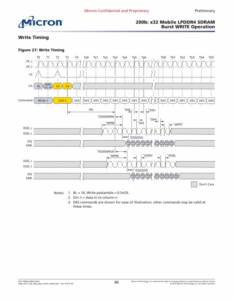
Write Timing
Figure 27: Write Timing
T0
CK_t
CK_cT1 T2 T3 T4 Ta0 Ta1 Tb0Ta2 Ta3 Ta4 Ta5 Ta6 Tb2 Tb3 Tb4 Tb5
CS
Tb1
CA BL
Command Write-1
BA0CA, AP CA
CAS-2
CA
WL
DES DES DES DES DES DESDES DES DES DES DES DES DES DES DES
t WPRE
tDQS2DQ
t WPST
DQS_t
DQS_c
Don’t Care
t WPRE
t DQSS(MIN)
t DSS
t DSS
t DSH
t DSH
t DQSH
t DQSS(MAX)
Dinn0
Dinn1
Dinn2
Dinn4
Dinn5
Din Din Din DinDinn3 n12 n13 n14 n15
t DQSL
tDQS2DQDQS_t
DQS_c
DQDMI
DQDMI
Dinn0
Dinn1
Dinn2
Dinn4
Din Din Din DinDinn3 n12
Dinn11 n13 n14 n15
Notes: 1. BL = 16, Write postamble = 0.5nCK.2. Din n = data-in to column.n3. DES commands are shown for ease of illustration; other commands may be valid at
these times.
Micron Confidential and Proprietary Preliminary
200b: x32 Mobile LPDDR4 SDRAMBurst WRITE Operation
PDF: 09005aef8653a92d200b_z01m_sdp_ddp_qdp_mobile_lpddr4.pdf – Rev. B 4/16 EN 80 Micron Technology, Inc. reserves the right to change products or specifications without notice.
© 2015 Micron Technology, Inc. All rights reserved.
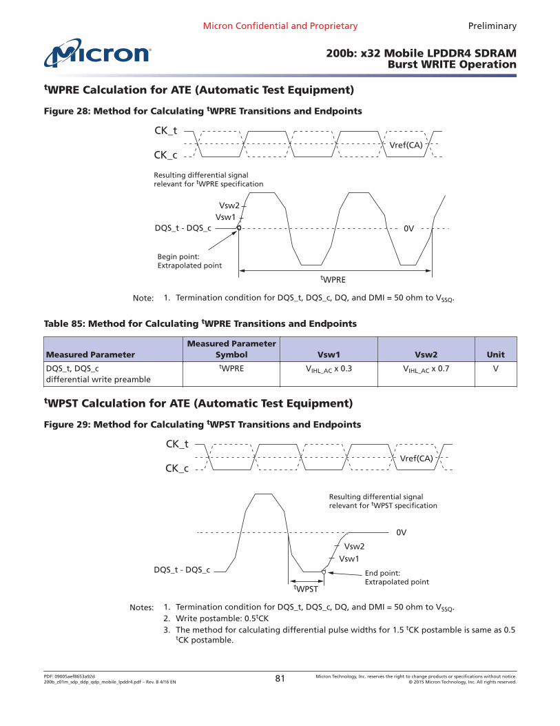
tWPRE Calculation for ATE (Automatic Test Equipment)
Figure 28: Method for Calculating tWPRE Transitions and Endpoints
CK_c
CK_tVref(CA)
Vsw2Vsw1
DQS_t - DQS_c
tWPRE
Begin point:Extrapolated point
Resulting differential signalrelevant for tWPRE specification
0V
Note: 1. Termination condition for DQS_t, DQS_c, DQ, and DMI = 50 ohm to VSSQ.
Table 85: Method for Calculating tWPRE Transitions and Endpoints
Measured ParameterMeasured Parameter
Symbol Vsw1 Vsw2 Unit
DQS_t, DQS_cdifferential write preamble
tWPRE VIHL_AC x 0.3 VIHL_AC x 0.7 V
tWPST Calculation for ATE (Automatic Test Equipment)
Figure 29: Method for Calculating tWPST Transitions and Endpoints
CK_c
CK_tVref(CA)
Vsw2Vsw1
DQS_t - DQS_c
tWPST
End point:Extrapolated point
Resulting differential signalrelevant for tWPST specification
0V
Notes: 1. Termination condition for DQS_t, DQS_c, DQ, and DMI = 50 ohm to VSSQ.2. Write postamble: 0.5tCK3. The method for calculating differential pulse widths for 1.5 tCK postamble is same as 0.5
tCK postamble.
Micron Confidential and Proprietary Preliminary
200b: x32 Mobile LPDDR4 SDRAMBurst WRITE Operation
PDF: 09005aef8653a92d200b_z01m_sdp_ddp_qdp_mobile_lpddr4.pdf – Rev. B 4/16 EN 81 Micron Technology, Inc. reserves the right to change products or specifications without notice.
© 2015 Micron Technology, Inc. All rights reserved.
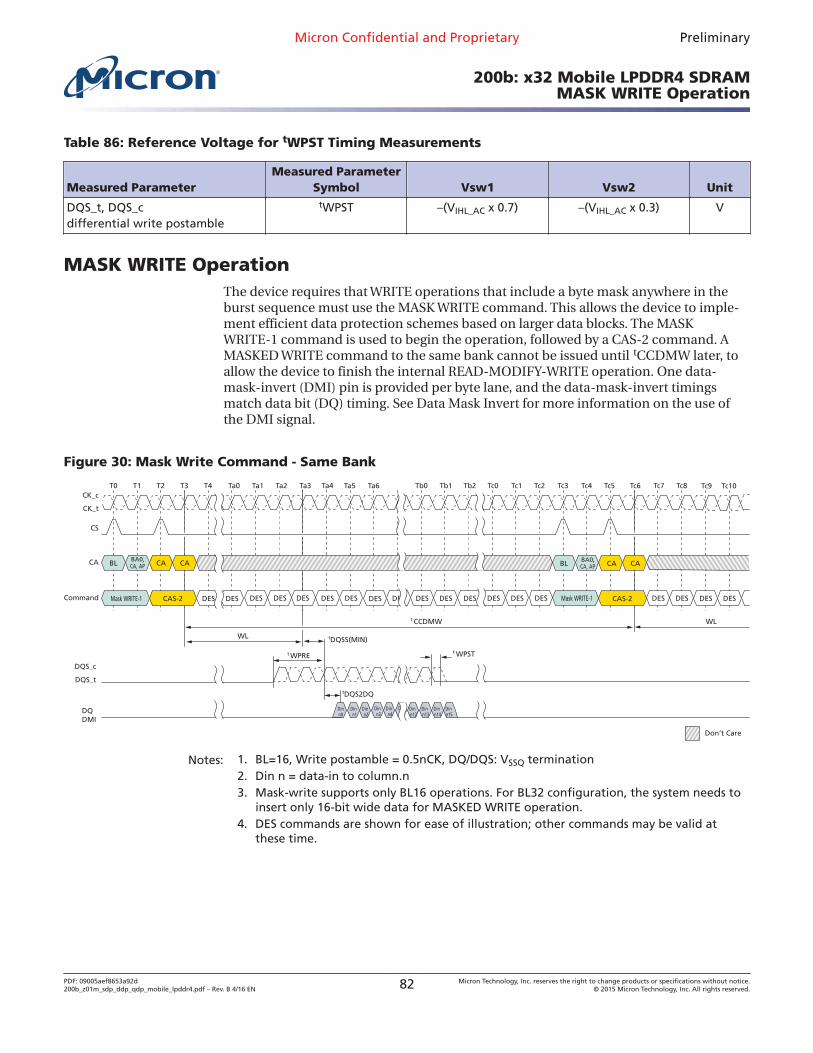
Table 86: Reference Voltage for tWPST Timing Measurements
Measured ParameterMeasured Parameter
Symbol Vsw1 Vsw2 Unit
DQS_t, DQS_cdifferential write postamble
tWPST –(VIHL_AC x 0.7) –(VIHL_AC x 0.3) V
MASK WRITE OperationThe device requires that WRITE operations that include a byte mask anywhere in theburst sequence must use the MASK WRITE command. This allows the device to imple-ment efficient data protection schemes based on larger data blocks. The MASKWRITE-1 command is used to begin the operation, followed by a CAS-2 command. AMASKED WRITE command to the same bank cannot be issued until tCCDMW later, toallow the device to finish the internal READ-MODIFY-WRITE operation. One data-mask-invert (DMI) pin is provided per byte lane, and the data-mask-invert timingsmatch data bit (DQ) timing. See Data Mask Invert for more information on the use ofthe DMI signal.
Figure 30: Mask Write Command - Same Bank
T0
CK_t
CK_cT1 T2 T3 T4 Tc1Tb1 Tc2Tb2Ta0 Ta1 Ta2 Ta3 Ta6 Tb0 Tc0 Tc4 Tc5Tc3 Tc7 Tc8Tc6
CS
Ta5Ta4
CA BL
Command Mask WRITE-1
BA0, CA
CAS-2
CA
WL
WL
DES DES
t WPRE
t CCDMW
tDQSS(MIN)
DQS_t
DQS_c
DQDMI
Don’t Care
tDQS2DQ
Dinn0
Dinn1
Dinn2
Dinn3
Dinn4
Dinn5
Dinn13
Dinn12
Dinn14
Dinn15
t WPST
DES DES DESDES DES DES DES DES DESDES DES DES DES
Tc10Tc9
DES DESCAS-2
BL BA0,CA, AP
DES DES
CA, AP CA CA
Mask WRITE-1
Notes: 1. BL=16, Write postamble = 0.5nCK, DQ/DQS: VSSQ termination2. Din n = data-in to column.n3. Mask-write supports only BL16 operations. For BL32 configuration, the system needs to
insert only 16-bit wide data for MASKED WRITE operation.4. DES commands are shown for ease of illustration; other commands may be valid at
these time.
Micron Confidential and Proprietary Preliminary
200b: x32 Mobile LPDDR4 SDRAMMASK WRITE Operation
PDF: 09005aef8653a92d200b_z01m_sdp_ddp_qdp_mobile_lpddr4.pdf – Rev. B 4/16 EN 82 Micron Technology, Inc. reserves the right to change products or specifications without notice.
© 2015 Micron Technology, Inc. All rights reserved.
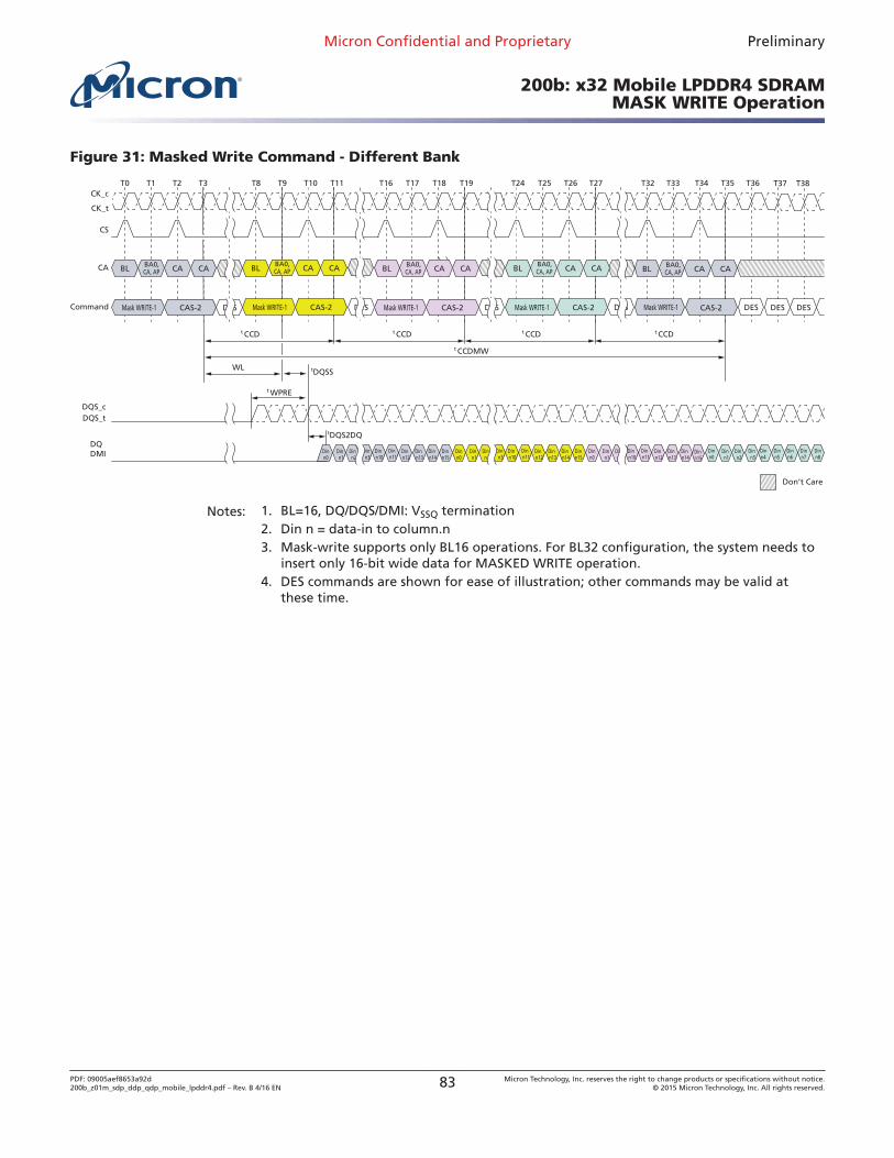
Figure 31: Masked Write Command - Different Bank
T0
CK_t
CK_cT1 T2 T3 T26T19 T27T24T8 T9 T10 T11 T17 T18 T25 T32 T33 T35 T36T34
CS
T16
CA BL
Command Mask WRITE-1
BA0, CA
CAS-2
CA
WL
DES
t WPRE
t CCD
tDQSS
DQS_tDQS_c
DQDMI
Don’t Care
tDQS2DQ
Dinn0
Dinn1
Dinn2
Dinn3
Dinn10
Dinn11
Dinn13
Dinn12
Dinn14
Dinn15
Dinn15
Dinn15
Dinn0
Dinn0
Dinn0
Dinn1
Dinn2
Dinn3
Dinn10
Dinn11
Dinn13
Dinn12
Dinn14
Dinn1
Dinn2
Dinn10
Dinn11
Dinn13
Dinn12
Dinn14
Dinn1
Dinn2
Dinn3
Dinn4
Dinn5
Dinn7
Dinn6
DES DESDES DES
T38T37
DES DESCAS-2
BL BA0,CA, APCA, AP BL
Mask WRITE-1
BA0, CA
CAS-2
CACA, AP BL
Mask WRITE-1
BA0, CA
CAS-2
CACA, AP BL
Mask WRITE-1
BA0, CA
CAS-2
CACA, AP CA CA
Mask WRITE-1
t CCD t CCDt CCD
t CCDMW
Dinn8
Notes: 1. BL=16, DQ/DQS/DMI: VSSQ termination2. Din n = data-in to column.n3. Mask-write supports only BL16 operations. For BL32 configuration, the system needs to
insert only 16-bit wide data for MASKED WRITE operation.4. DES commands are shown for ease of illustration; other commands may be valid at
these time.
Micron Confidential and Proprietary Preliminary
200b: x32 Mobile LPDDR4 SDRAMMASK WRITE Operation
PDF: 09005aef8653a92d200b_z01m_sdp_ddp_qdp_mobile_lpddr4.pdf – Rev. B 4/16 EN 83 Micron Technology, Inc. reserves the right to change products or specifications without notice.
© 2015 Micron Technology, Inc. All rights reserved.
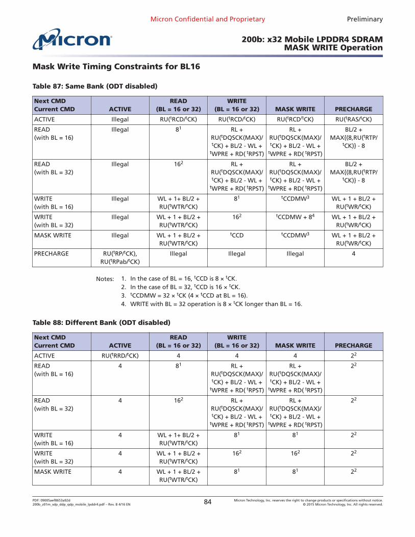
Mask Write Timing Constraints for BL16
Table 87: Same Bank (ODT disabled)
Next CMDCurrent CMD ACTIVE
READ(BL = 16 or 32)
WRITE(BL = 16 or 32) MASK WRITE PRECHARGE
ACTIVE Illegal RU(tRCD/tCK) RU(tRCD/tCK) RU(tRCD/tCK) RU(tRAS/tCK)
READ(with BL = 16)
Illegal 81 RL +RU(tDQSCK(MAX)/tCK) + BL/2 - WL +
tWPRE + RD( tRPST)
RL +RU(tDQSCK(MAX)/tCK) + BL/2 - WL +
tWPRE + RD( tRPST)
BL/2 +MAX{(8,RU(tRTP/
tCK)} - 8
READ(with BL = 32)
Illegal 162 RL +RU(tDQSCK(MAX)/tCK) + BL/2 - WL +
tWPRE + RD( tRPST)
RL +RU(tDQSCK(MAX)/tCK) + BL/2 - WL +
tWPRE + RD( tRPST)
BL/2 +MAX{(8,RU(tRTP/
tCK)} - 8
WRITE(with BL = 16)
Illegal WL + 1+ BL/2 +RU(tWTR/tCK)
81 tCCDMW3 WL + 1 + BL/2 +RU(tWR/tCK)
WRITE(with BL = 32)
Illegal WL + 1 + BL/2 +RU(tWTR/tCK)
162 tCCDMW + 84 WL + 1 + BL/2 +RU(tWR/tCK)
MASK WRITE Illegal WL + 1 + BL/2 +RU(tWTR/tCK)
tCCD tCCDMW3 WL + 1 + BL/2 +RU(tWR/tCK)
PRECHARGE RU(tRP/tCK),RU(tRPab/tCK)
Illegal Illegal Illegal 4
Notes: 1. In the case of BL = 16, tCCD is 8 × tCK.2. In the case of BL = 32, tCCD is 16 × tCK.3. tCCDMW = 32 × tCK (4 × tCCD at BL = 16).4. WRITE with BL = 32 operation is 8 × tCK longer than BL = 16.
Table 88: Different Bank (ODT disabled)
Next CMDCurrent CMD ACTIVE
READ(BL = 16 or 32)
WRITE(BL = 16 or 32) MASK WRITE PRECHARGE
ACTIVE RU(tRRD/tCK) 4 4 4 22
READ(with BL = 16)
4 81 RL +RU(tDQSCK(MAX)/tCK) + BL/2 - WL +
tWPRE + RD( tRPST)
RL +RU(tDQSCK(MAX)/tCK) + BL/2 - WL +
tWPRE + RD( tRPST)
22
READ(with BL = 32)
4 162 RL +RU(tDQSCK(MAX)/tCK) + BL/2 - WL +
tWPRE + RD( tRPST)
RL +RU(tDQSCK(MAX)/tCK) + BL/2 - WL +
tWPRE + RD( tRPST)
22
WRITE(with BL = 16)
4 WL + 1+ BL/2 +RU(tWTR/tCK)
81 81 22
WRITE(with BL = 32)
4 WL + 1 + BL/2 +RU(tWTR/tCK)
162 162 22
MASK WRITE 4 WL + 1 + BL/2 +RU(tWTR/tCK)
81 81 22
Micron Confidential and Proprietary Preliminary
200b: x32 Mobile LPDDR4 SDRAMMASK WRITE Operation
PDF: 09005aef8653a92d200b_z01m_sdp_ddp_qdp_mobile_lpddr4.pdf – Rev. B 4/16 EN 84 Micron Technology, Inc. reserves the right to change products or specifications without notice.
© 2015 Micron Technology, Inc. All rights reserved.
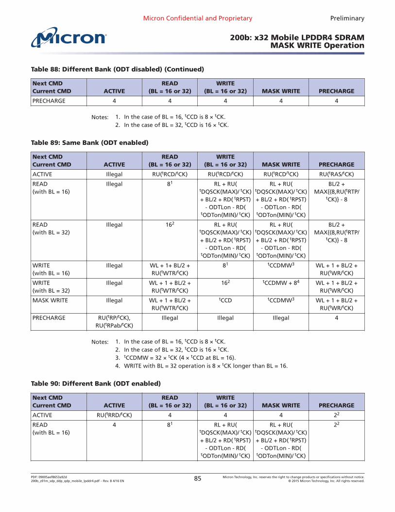
Table 88: Different Bank (ODT disabled) (Continued)
Next CMDCurrent CMD ACTIVE
READ(BL = 16 or 32)
WRITE(BL = 16 or 32) MASK WRITE PRECHARGE
PRECHARGE 4 4 4 4 4
Notes: 1. In the case of BL = 16, tCCD is 8 × tCK.2. In the case of BL = 32, tCCD is 16 × tCK.
Table 89: Same Bank (ODT enabled)
Next CMDCurrent CMD ACTIVE
READ(BL = 16 or 32)
WRITE(BL = 16 or 32) MASK WRITE PRECHARGE
ACTIVE Illegal RU(tRCD/tCK) RU(tRCD/tCK) RU(tRCD/tCK) RU(tRAS/tCK)
READ(with BL = 16)
Illegal 81 RL + RU(tDQSCK(MAX)/ tCK)+ BL/2 + RD( tRPST)
- ODTLon - RD(tODTon(MIN)/ tCK)
RL + RU(tDQSCK(MAX)/ tCK)+ BL/2 + RD( tRPST)
- ODTLon - RD(tODTon(MIN)/ tCK)
BL/2 +MAX{(8,RU(tRTP/
tCK)} - 8
READ(with BL = 32)
Illegal 162 RL + RU(tDQSCK(MAX)/ tCK)+ BL/2 + RD( tRPST)
- ODTLon - RD(tODTon(MIN)/ tCK)
RL + RU(tDQSCK(MAX)/ tCK)+ BL/2 + RD( tRPST)
- ODTLon - RD(tODTon(MIN)/ tCK)
BL/2 +MAX{(8,RU(tRTP/
tCK)} - 8
WRITE(with BL = 16)
Illegal WL + 1+ BL/2 +RU(tWTR/tCK)
81 tCCDMW3 WL + 1 + BL/2 +RU(tWR/tCK)
WRITE(with BL = 32)
Illegal WL + 1 + BL/2 +RU(tWTR/tCK)
162 tCCDMW + 84 WL + 1 + BL/2 +RU(tWR/tCK)
MASK WRITE Illegal WL + 1 + BL/2 +RU(tWTR/tCK)
tCCD tCCDMW3 WL + 1 + BL/2 +RU(tWR/tCK)
PRECHARGE RU(tRP/tCK),RU(tRPab/tCK)
Illegal Illegal Illegal 4
Notes: 1. In the case of BL = 16, tCCD is 8 × tCK.2. In the case of BL = 32, tCCD is 16 × tCK.3. tCCDMW = 32 × tCK (4 × tCCD at BL = 16).4. WRITE with BL = 32 operation is 8 × tCK longer than BL = 16.
Table 90: Different Bank (ODT enabled)
Next CMDCurrent CMD ACTIVE
READ(BL = 16 or 32)
WRITE(BL = 16 or 32) MASK WRITE PRECHARGE
ACTIVE RU(tRRD/tCK) 4 4 4 22
READ(with BL = 16)
4 81 RL + RU(tDQSCK(MAX)/ tCK)+ BL/2 + RD( tRPST)
- ODTLon - RD(tODTon(MIN)/ tCK)
RL + RU(tDQSCK(MAX)/ tCK)+ BL/2 + RD( tRPST)
- ODTLon - RD(tODTon(MIN)/ tCK)
22
Micron Confidential and Proprietary Preliminary
200b: x32 Mobile LPDDR4 SDRAMMASK WRITE Operation
PDF: 09005aef8653a92d200b_z01m_sdp_ddp_qdp_mobile_lpddr4.pdf – Rev. B 4/16 EN 85 Micron Technology, Inc. reserves the right to change products or specifications without notice.
© 2015 Micron Technology, Inc. All rights reserved.
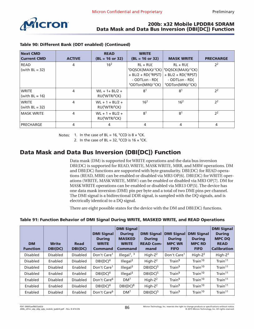
Table 90: Different Bank (ODT enabled) (Continued)
Next CMDCurrent CMD ACTIVE
READ(BL = 16 or 32)
WRITE(BL = 16 or 32) MASK WRITE PRECHARGE
READ(with BL = 32)
4 162 RL + RU(tDQSCK(MAX)/ tCK)+ BL/2 + RD( tRPST)
- ODTLon - RD(tODTon(MIN)/ tCK)
RL + RU(tDQSCK(MAX)/ tCK)+ BL/2 + RD( tRPST)
- ODTLon - RD(tODTon(MIN)/ tCK)
22
WRITE(with BL = 16)
4 WL + 1+ BL/2 +RU(tWTR/tCK)
81 81 22
WRITE(with BL = 32)
4 WL + 1 + BL/2 +RU(tWTR/tCK)
162 162 22
MASK WRITE 4 WL + 1 + BL/2 +RU(tWTR/tCK)
81 81 22
PRECHARGE 4 4 4 4 4
Notes: 1. In the case of BL = 16, tCCD is 8 × tCK.2. In the case of BL = 32, tCCD is 16 × tCK.
Data Mask and Data Bus Inversion (DBI[DC]) FunctionData mask (DM) is supported for WRITE operations and the data bus inversionDBI(DC) is supported for READ, WRITE, MASK WRITE, MRR, and MRW operations. DMand DBI(DC) functions are supported with byte granularity. DBI(DC) for READ opera-tions (READ, MRR) can be enabled or disabled via MR3 OP[6]. DBI(DC) for WRITE oper-ations (WRITE, MASK WRITE, MRW) can be enabled or disabled via MR3 OP[7]. DM forMASK WRITE operations can be enabled or disabled via MR13 OP[5]. The device hasone data mask inversion (DMI) pin per byte and a total of two DMI pins per channel.The DMI signal is a bidirectional DDR signal, is sampled with the DQ signals, and iselectrically identical to a DQ signal.
There are eight possible states for the device with the DM and DBI(DC) functions.
Table 91: Function Behavior of DMI Signal During WRITE, MASKED WRITE, and READ Operations
DMFunction
WriteDBI(DC)
ReadDBI(DC)
DMI SignalDuringWRITE
Command
DMI SignalDuring
MASKEDWRITE
Command
DMI SignalDuring
READ Com-mand
DMI SignalDuring
MPC WRFIFO
DMI SignalDuringMPC RD
FIFO
DMI SignalDuringMPC DQ
READCalibration
Disabled Disabled Disabled Don't Care1 Illegal1, 3 High-Z2 Don't Care1 High-Z2 High-Z2
Disabled Enabled Disabled DBI(DC)4 Illegal3 High-Z2 Train9 Train10 Train11
Disabled Disabled Enabled Don't Care1 Illegal3 DBI(DC)5 Train9 Train10 Train11
Disabled Enabled Enabled DBI(DC)4 Illegal3 DBI(DC)5 Train9 Train10 Train11
Enabled Disabled Disabled Don't Care6 DM7 High-Z2 Train9 Train10 Train11
Enabled Enabled Disabled DBI(DC)4 DBI(DC)8 High-Z2 Train9 Train10 Train11
Enabled Disabled Enabled Don't Care6 DM7 DBI(DC)5 Train9 Train10 Train11
Micron Confidential and Proprietary Preliminary
200b: x32 Mobile LPDDR4 SDRAMData Mask and Data Bus Inversion (DBI[DC]) Function
PDF: 09005aef8653a92d200b_z01m_sdp_ddp_qdp_mobile_lpddr4.pdf – Rev. B 4/16 EN 86 Micron Technology, Inc. reserves the right to change products or specifications without notice.
© 2015 Micron Technology, Inc. All rights reserved.
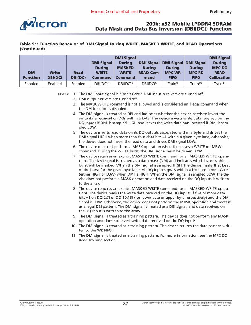
Table 91: Function Behavior of DMI Signal During WRITE, MASKED WRITE, and READ Operations(Continued)
DMFunction
WriteDBI(DC)
ReadDBI(DC)
DMI SignalDuringWRITE
Command
DMI SignalDuring
MASKEDWRITE
Command
DMI SignalDuring
READ Com-mand
DMI SignalDuring
MPC WRFIFO
DMI SignalDuringMPC RD
FIFO
DMI SignalDuringMPC DQ
READCalibration
Enabled Enabled Enabled DBI(DC)4 DBI(DC)8 DBI(DC)5 Train9 Train10 Train11
Notes: 1. The DMI input signal is "Don’t Care." DMI input receivers are turned off.2. DMI output drivers are turned off.3. The MASK WRITE command is not allowed and is considered an illegal command when
the DM function is disabled.4. The DMI signal is treated as DBI and indicates whether the device needs to invert the
write data received on DQs within a byte. The device inverts write data received on theDQ inputs if DMI is sampled HIGH and leaves the write data non-inverted if DMI is sam-pled LOW.
5. The device inverts read data on its DQ outputs associated within a byte and drives theDMI signal HIGH when more than four data bits =1 within a given byte lane; otherwise,the device does not invert the read data and drives DMI signal LOW.
6. The device does not perform a MASK operation when it receives a WRITE (or MRW)command. During the WRITE burst, the DMI signal must be driven LOW.
7. The device requires an explicit MASKED WRITE command for all MASKED WRITE opera-tions. The DMI signal is treated as a data mask (DM) and indicates which bytes within aburst will be masked. When the DMI signal is sampled HIGH, the device masks that beatof the burst for the given byte lane. All DQ input signals within a byte are "Don't Care"(either HIGH or LOW) when DMI is HIGH. When the DMI signal is sampled LOW, the de-vice does not perform a MASK operation and data received on the DQ inputs is writtento the array.
8. The device requires an explicit MASKED WRITE command for all MASKED WRITE opera-tions. The device masks the write data received on the DQ inputs if five or more databits =1 on DQ[2:7] or DQ[10:15] (for lower byte or upper byte respectively) and the DMIsignal is LOW. Otherwise, the device does not perform the MASK operation and treats itas a legal DBI pattern. The DMI signal is treated as a DBI signal, and data received onthe DQ input is written to the array.
9. The DMI signal is treated as a training pattern. The device does not perform any MASKoperation and does not invert write data received on the DQ inputs.
10. The DMI signal is treated as a training pattern. The device returns the data pattern writ-ten to the WR FIFO.
11. The DMI signal is treated as a training pattern. For more information, see the MPC DQRead Training section.
Micron Confidential and Proprietary Preliminary
200b: x32 Mobile LPDDR4 SDRAMData Mask and Data Bus Inversion (DBI[DC]) Function
PDF: 09005aef8653a92d200b_z01m_sdp_ddp_qdp_mobile_lpddr4.pdf – Rev. B 4/16 EN 87 Micron Technology, Inc. reserves the right to change products or specifications without notice.
© 2015 Micron Technology, Inc. All rights reserved.
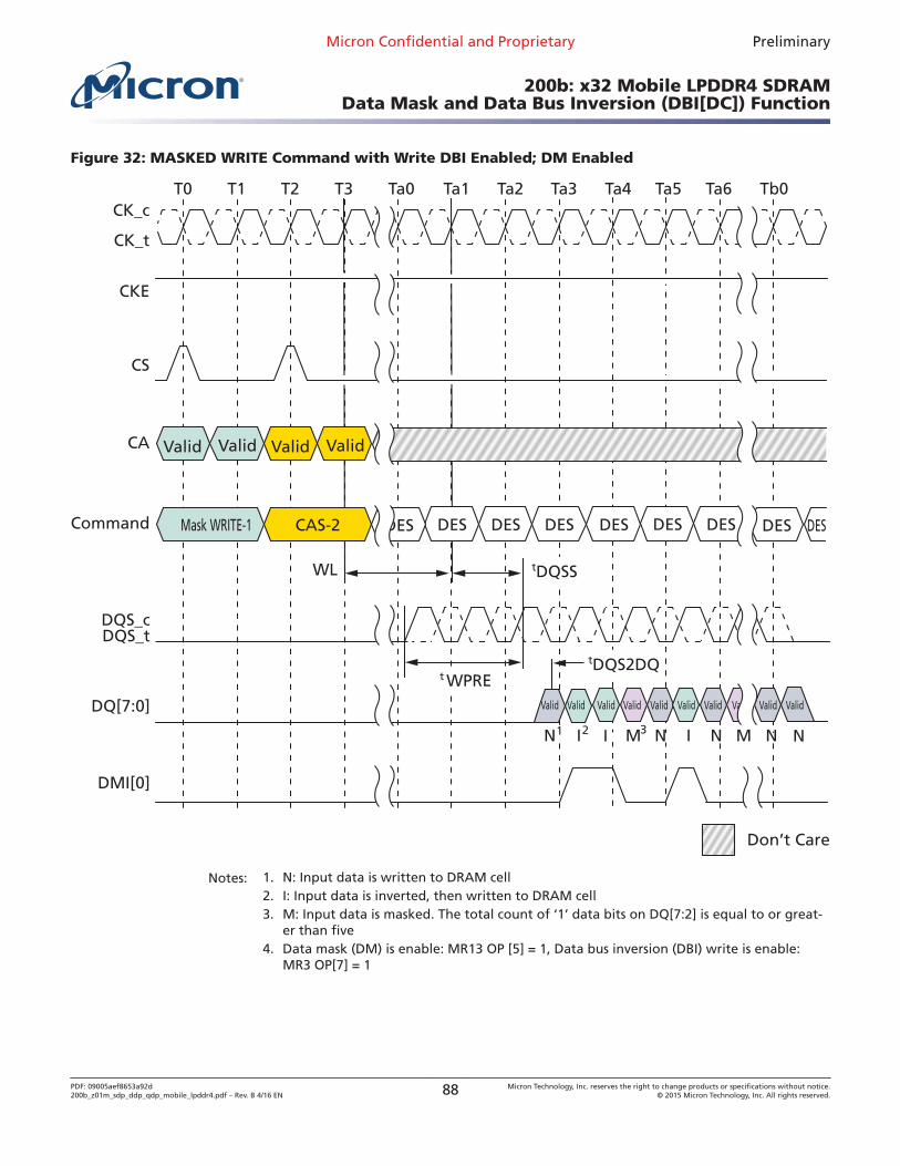
Figure 32: MASKED WRITE Command with Write DBI Enabled; DM Enabled
T0
CK_t
CK_cT1 T2 T3 Ta0 Ta1 Ta2 Ta3 Ta4 Tb0
CS
CKE
Ta6Ta5
CA Valid
Command Mask WRITE-1 CAS-2
WL
DQS_tDQS_c
DQ[7:0]
DMI[0]
Don’t Care
tDQS2DQ
Valid
N N N N N
Valid
I II
DES DESDES DES DES DES DES DES
Valid Valid Valid
tDQSS
DES
Valid Valid
M M
Valid Valid Valid Valid Valid Valid
t WPRE
1 2 3
Notes: 1. N: Input data is written to DRAM cell2. I: Input data is inverted, then written to DRAM cell3. M: Input data is masked. The total count of ‘1’ data bits on DQ[7:2] is equal to or great-
er than five4. Data mask (DM) is enable: MR13 OP [5] = 1, Data bus inversion (DBI) write is enable:
MR3 OP[7] = 1
Micron Confidential and Proprietary Preliminary
200b: x32 Mobile LPDDR4 SDRAMData Mask and Data Bus Inversion (DBI[DC]) Function
PDF: 09005aef8653a92d200b_z01m_sdp_ddp_qdp_mobile_lpddr4.pdf – Rev. B 4/16 EN 88 Micron Technology, Inc. reserves the right to change products or specifications without notice.
© 2015 Micron Technology, Inc. All rights reserved.
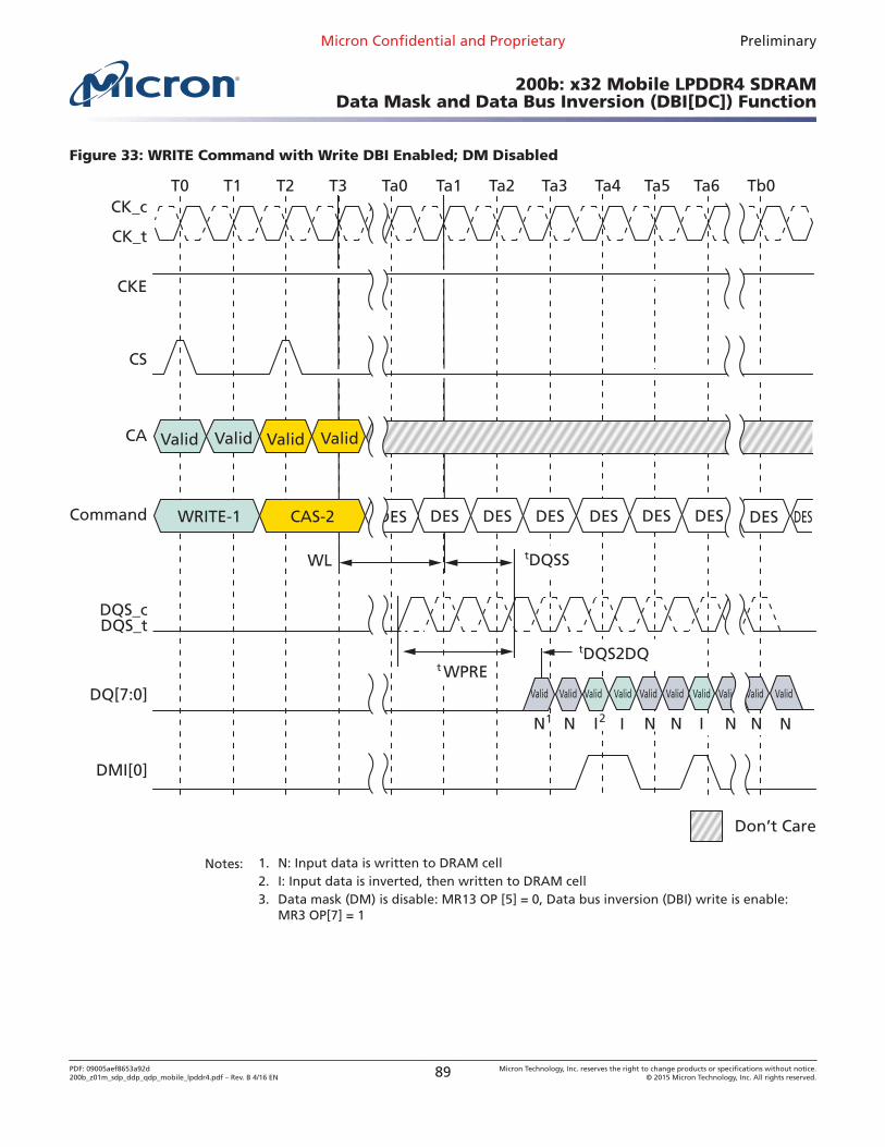
Figure 33: WRITE Command with Write DBI Enabled; DM Disabled
T0
CK_t
CK_cT1 T2 T3 Ta0 Ta1 Ta2 Ta3 Ta4 Tb0
CS
CKE
Ta6Ta5
CA Valid
Command WRITE-1 CAS-2
WL
DQS_tDQS_c
DQ[7:0]
DMI[0]
Don’t Care
tDQS2DQ
Valid
N N N N N N
Valid Valid
I II
DES DESDES DES DES DES DES DES
Valid Valid Valid
tDQSS
DES
Valid Valid Valid Valid Valid Valid Valid
t WPRE
1 2 N
Notes: 1. N: Input data is written to DRAM cell2. I: Input data is inverted, then written to DRAM cell3. Data mask (DM) is disable: MR13 OP [5] = 0, Data bus inversion (DBI) write is enable:
MR3 OP[7] = 1
Micron Confidential and Proprietary Preliminary
200b: x32 Mobile LPDDR4 SDRAMData Mask and Data Bus Inversion (DBI[DC]) Function
PDF: 09005aef8653a92d200b_z01m_sdp_ddp_qdp_mobile_lpddr4.pdf – Rev. B 4/16 EN 89 Micron Technology, Inc. reserves the right to change products or specifications without notice.
© 2015 Micron Technology, Inc. All rights reserved.
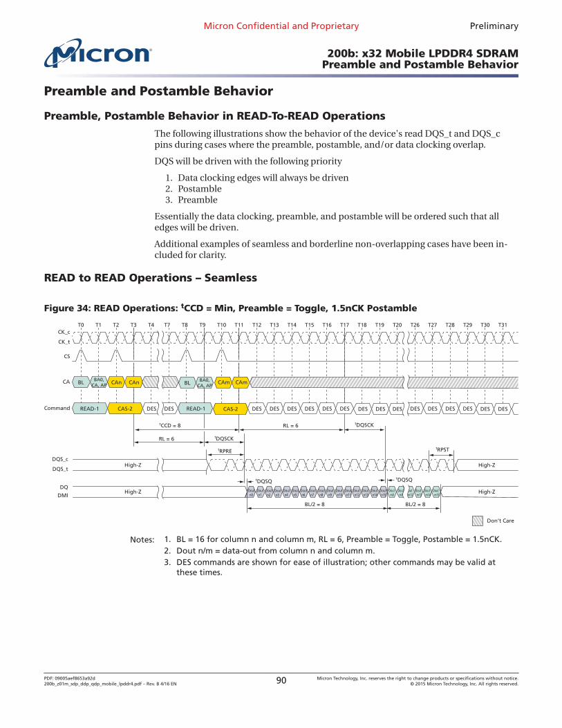
Preamble and Postamble Behavior
Preamble, Postamble Behavior in READ-To-READ Operations
The following illustrations show the behavior of the device's read DQS_t and DQS_cpins during cases where the preamble, postamble, and/or data clocking overlap.
DQS will be driven with the following priority
1. Data clocking edges will always be driven2. Postamble3. Preamble
Essentially the data clocking, preamble, and postamble will be ordered such that alledges will be driven.
Additional examples of seamless and borderline non-overlapping cases have been in-cluded for clarity.
READ to READ Operations – Seamless
Figure 34: READ Operations: tCCD = Min, Preamble = Toggle, 1.5nCK Postamble
T0
CK_t
CK_cT1 T2 T3 T4 T7 T20T8 T13T9 T10 T11 T12 T15 T16 T17 T18 T19
CS
T14
CA BL
Command READ-1
BA0,CA, AP CAn
CAS-2
CAn CAm CAm
RL = 6
RL = 6
DES DES DES DES DES DES DES DES DES DES DES
tRPRE
tDQSCK
tDQSCKtCCD = 8
tRPST
tDQSQ
DQS_t
DQS_c
Don’t Care
tDQSQ
T31T26 T27 T28 T29 T30
DES DES DES DES DES DESCAS-2
Doutn0
Doutn1
Doutn2
Doutn4
Doutn6
Doutn7
Doutn8
Doutn9
Doutn10
Doutn5
Doutn12
Doutm0
Doutn13
Doutn14
Doutn15
Doutn3
Doutm1
Doutm12
Doutm14
Doutm15
Doutm13
Doutn11
High-Z
High-Z
High-Z
BL BA0,CA, AP
READ-1
High-Z
BL/2 = 8 BL/2 = 8
DQ
DMI
Notes: 1. BL = 16 for column n and column m, RL = 6, Preamble = Toggle, Postamble = 1.5nCK.2. Dout n/m = data-out from column n and column m.3. DES commands are shown for ease of illustration; other commands may be valid at
these times.
Micron Confidential and Proprietary Preliminary
200b: x32 Mobile LPDDR4 SDRAMPreamble and Postamble Behavior
PDF: 09005aef8653a92d200b_z01m_sdp_ddp_qdp_mobile_lpddr4.pdf – Rev. B 4/16 EN 90 Micron Technology, Inc. reserves the right to change products or specifications without notice.
© 2015 Micron Technology, Inc. All rights reserved.
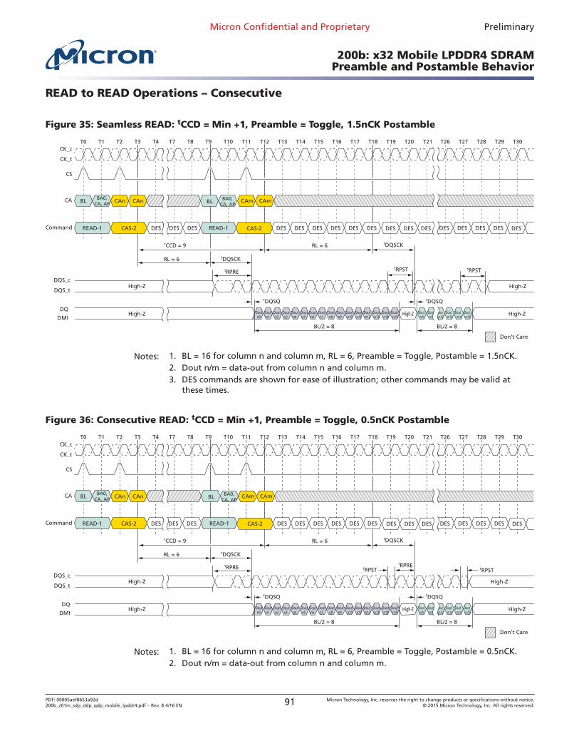
READ to READ Operations – Consecutive
Figure 35: Seamless READ: tCCD = Min +1, Preamble = Toggle, 1.5nCK Postamble
T0
CK_t
CK_cT1 T2 T3 T4 T7 T20T8 T13T9 T10 T11 T12 T15 T16 T17 T18 T19
CS
T14
CA BL
Command READ-1
BA0,CA, AP CAn
CAS-2
CAn CAm CAm
RL = 6
RL = 6
BL/2 = 8
DES DES DES DES DES DES DES DES DES DES DES
tRPRE
tDQSCK
tDQSCKtCCD = 9
tRPST
tDQSQ
DQS_t
DQS_c
Don’t Care
tDQSQ
T21 T26 T27 T28 T29 T30
DES DES DES DES DESCAS-2
Doutn0
Doutn1
Doutn2
Doutn4
Doutn6
Doutn7
Doutn8
Doutn9
Doutn10
Doutn5
Doutn12
Doutm0
Doutn13
Doutn14
Doutn15
Doutn3
Doutm1
Doutm12
Doutm14
Doutm15
Doutm13
Doutn11
High-Z
High-Z
High-Z High-Z
tRPST
BL BA0,CA, AP
READ-1
High-Z
BL/2 = 8
DES
DQ
DMI
Notes: 1. BL = 16 for column n and column m, RL = 6, Preamble = Toggle, Postamble = 1.5nCK.2. Dout n/m = data-out from column n and column m.3. DES commands are shown for ease of illustration; other commands may be valid at
these times.
Figure 36: Consecutive READ: tCCD = Min +1, Preamble = Toggle, 0.5nCK Postamble
T0
CK_t
CK_cT1 T2 T3 T4 T7 T20T8 T13T9 T10 T11 T12 T15 T16 T17 T18 T19
CS
T14
CA BL
Command READ-1
BA0,CA, AP CAn
CAS-2
CAn CAm CAm
RL = 6
RL = 6
BL/2 = 8
DES DES DES DES DES DES DES DES DES DES DES
tRPREtRPRE
tDQSCK
tDQSCKtCCD = 9
tRPST
tDQSQ
DQS_t
DQS_c
Don’t Care
tDQSQ
T21 T26 T27 T28 T29 T30
DES DES DES DES DESCAS-2
Doutn0
Doutn1
Doutn2
Doutn4
Doutn6
Doutn7
Doutn8
Doutn9
Doutn10
Doutn5
Doutn12
Doutm0
Doutn13
Doutn14
Doutn15
Doutn3
Doutm1
Doutm12
Doutm14
Doutm15
Doutm13
Doutn11
High-Z
High-Z
High-Z High-Z
tRPST
BL BA0,CA, AP
READ-1
High-Z
BL/2 = 8
DES
DQ
DMI
Notes: 1. BL = 16 for column n and column m, RL = 6, Preamble = Toggle, Postamble = 0.5nCK.2. Dout n/m = data-out from column n and column m.
Micron Confidential and Proprietary Preliminary
200b: x32 Mobile LPDDR4 SDRAMPreamble and Postamble Behavior
PDF: 09005aef8653a92d200b_z01m_sdp_ddp_qdp_mobile_lpddr4.pdf – Rev. B 4/16 EN 91 Micron Technology, Inc. reserves the right to change products or specifications without notice.
© 2015 Micron Technology, Inc. All rights reserved.
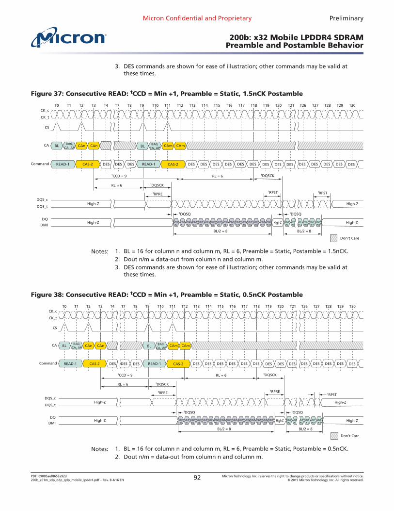
3. DES commands are shown for ease of illustration; other commands may be valid atthese times.
Figure 37: Consecutive READ: tCCD = Min +1, Preamble = Static, 1.5nCK Postamble
T0
CK_t
CK_cT1 T2 T3 T4 T7 T20T8 T13T9 T10 T11 T12 T15 T16 T17 T18 T19
CS
T14
CA BL
Command READ-1
BA0,CA, AP CAn
CAS-2
CAn CAm CAm
RL = 6
RL = 6
BL/2 = 8
DES DES DES DES DES DES DES DES DES DES DES
tRPRE
tDQSCK
tDQSCKtCCD = 9
tRPST
tDQSQ
DQS_t
DQS_c
Don’t Care
tDQSQ
T21 T26 T27 T28 T29 T30
DES DES DES DES DESCAS-2
Doutn0
Doutn1
Doutn2
Doutn4
Doutn6
Doutn7
Doutn8
Doutn9
Doutn10
Doutn5
Doutn12
Doutm0
Doutn13
Doutn14
Doutn15
Doutn3
Doutm1
Doutm12
Doutm14
Doutm15
Doutm13
Doutn11
High-Z
High-Z
High-Z High-Z
tRPST
BL BA0,CA, AP
READ-1
High-Z
BL/2 = 8
DES
DQ
DMI
Notes: 1. BL = 16 for column n and column m, RL = 6, Preamble = Static, Postamble = 1.5nCK.2. Dout n/m = data-out from column n and column m.3. DES commands are shown for ease of illustration; other commands may be valid at
these times.
Figure 38: Consecutive READ: tCCD = Min +1, Preamble = Static, 0.5nCK Postamble
T0
CK_t
CK_cT1 T2 T3 T4 T7 T20T8 T13T9 T10 T11 T12 T15 T16 T17 T18 T19
CS
T14
CA BL
Command READ-1
BA0,CA, AP CAn
CAS-2
CAn CAm CAm
RL = 6
RL = 6
BL/2 = 8
DES DES DES DES DES DES DES DES DES DES DES
tRPREtRPRE
tDQSCK
tDQSCKtCCD = 9
tRPST
tDQSQ
DQS_t
DQS_c
DQ
DMI
Don’t Care
tDQSQ
T21 T26 T27 T28 T29 T30
DES DES DES DES DESCAS-2
Doutn0
Doutn1
Doutn2
Doutn4
Doutn6
Doutn7
Doutn8
Doutn9
Doutn10
Doutn5
Doutn12
Doutm0
Doutn13
Doutn14
Doutn15
Doutn3
Doutm1
Doutm12
Doutm14
Doutm15
Doutm13
Doutn11
High-Z
High-Z
High-Z High-Z
BL BA0,CA, AP
READ-1
High-Z
BL/2 = 8
DES
Notes: 1. BL = 16 for column n and column m, RL = 6, Preamble = Static, Postamble = 0.5nCK.2. Dout n/m = data-out from column n and column m.
Micron Confidential and Proprietary Preliminary
200b: x32 Mobile LPDDR4 SDRAMPreamble and Postamble Behavior
PDF: 09005aef8653a92d200b_z01m_sdp_ddp_qdp_mobile_lpddr4.pdf – Rev. B 4/16 EN 92 Micron Technology, Inc. reserves the right to change products or specifications without notice.
© 2015 Micron Technology, Inc. All rights reserved.
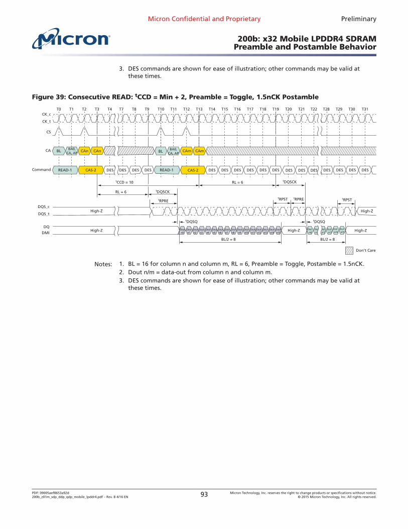
3. DES commands are shown for ease of illustration; other commands may be valid atthese times.
Figure 39: Consecutive READ: tCCD = Min + 2, Preamble = Toggle, 1.5nCK Postamble
T0
CK_t
CK_cT1 T2 T3 T4 T7 T20T8 T13T9 T10 T11 T12 T15 T16 T17 T18 T19
CS
T14
CA BL
Command READ-1
BA0,CA, AP CAn
CAS-2
CAn CAm CAm
RL = 6
RL = 6
BL/2 = 8
DES DES DES DES DES DES DES DES DES DES DES
tRPREtRPRE
tDQSCK
tDQSCKtCCD = 10
tRPST
tDQSQ
DQS_t
DQS_c
DQ
DMI
Don’t Care
tDQSQ
T21 T22 T31T28 T29 T30
DES DES DES DESCAS-2
Doutn0
Doutn1
Doutn2
Doutn4
Doutn6
Doutn7
Doutn8
Doutn9
Doutn10
Doutn5
Doutn12
Doutm0
Doutn13
Doutn14
Doutn15
Doutn3
Doutm1
Doutm12
Doutm14
Doutm15
Doutm13
Doutn11
High-Z
High-Z
High-Z High-Z
tRPST
BL BA0,CA, AP
READ-1
High-Z
BL/2 = 8
DES DES
Notes: 1. BL = 16 for column n and column m, RL = 6, Preamble = Toggle, Postamble = 1.5nCK.2. Dout n/m = data-out from column n and column m.3. DES commands are shown for ease of illustration; other commands may be valid at
these times.
Micron Confidential and Proprietary Preliminary
200b: x32 Mobile LPDDR4 SDRAMPreamble and Postamble Behavior
PDF: 09005aef8653a92d200b_z01m_sdp_ddp_qdp_mobile_lpddr4.pdf – Rev. B 4/16 EN 93 Micron Technology, Inc. reserves the right to change products or specifications without notice.
© 2015 Micron Technology, Inc. All rights reserved.
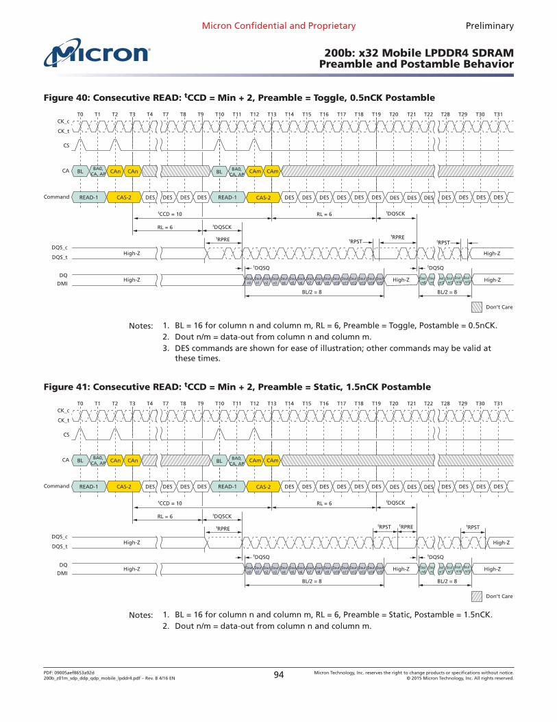
Figure 40: Consecutive READ: tCCD = Min + 2, Preamble = Toggle, 0.5nCK Postamble
T0
CK_t
CK_cT1 T2 T3 T4 T7 T20T8 T13T9 T10 T11 T12 T15 T16 T17 T18 T19
CS
T14
CA BL
Command READ-1
BA0,CA, AP CAn
CAS-2
CAn CAm CAm
RL = 6
RL = 6
BL/2 = 8
DES DES DES DES DES DES DES DES DES DES DES
tRPREtRPRE
tDQSCK
tDQSCKtCCD = 10
tRPST
tDQSQ
DQS_t
DQS_c
Don’t Care
tDQSQ
T21 T22 T31T28 T29 T30
DES DES DES DESCAS-2
Doutn0
Doutn1
Doutn2
Doutn4
Doutn6
Doutn7
Doutn8
Doutn9
Doutn10
Doutn5
Doutn12
Doutm0
Doutn13
Doutn14
Doutn15
Doutn3
Doutm1
Doutm12
Doutm14
Doutm15
Doutm13
Doutn11
High-Z
High-Z
High-Z High-Z
tRPST
BL BA0,CA, AP
READ-1
High-Z
BL/2 = 8
DES DES
DQ
DMI
Notes: 1. BL = 16 for column n and column m, RL = 6, Preamble = Toggle, Postamble = 0.5nCK.2. Dout n/m = data-out from column n and column m.3. DES commands are shown for ease of illustration; other commands may be valid at
these times.
Figure 41: Consecutive READ: tCCD = Min + 2, Preamble = Static, 1.5nCK Postamble
T0
CK_t
CK_cT1 T2 T3 T4 T7 T20T8 T13T9 T10 T11 T12 T15 T16 T17 T18 T19
CS
T14
CA BL
Command READ-1
BA0,CA, AP CAn
CAS-2
CAn CAm CAm
RL = 6
RL = 6
BL/2 = 8
DES DES DES DES DES DES DES DES DES DES DES
tRPREtRPRE
tDQSCK
tDQSCKtCCD = 10
tRPST
tDQSQ
DQS_t
DQS_c
Don’t Care
tDQSQ
T21 T22 T31T28 T29 T30
DES DES DES DESCAS-2
Doutn0
Doutn1
Doutn2
Doutn4
Doutn6
Doutn7
Doutn8
Doutn9
Doutn10
Doutn5
Doutn12
Doutm0
Doutn13
Doutn14
Doutn15
Doutn3
Doutm1
Doutm12
Doutm14
Doutm15
Doutm13
Doutn11
High-Z
High-Z
High-Z High-Z
tRPST
BL BA0,CA, AP
READ-1
High-Z
BL/2 = 8
DES DES
DQ
DMI
Notes: 1. BL = 16 for column n and column m, RL = 6, Preamble = Static, Postamble = 1.5nCK.2. Dout n/m = data-out from column n and column m.
Micron Confidential and Proprietary Preliminary
200b: x32 Mobile LPDDR4 SDRAMPreamble and Postamble Behavior
PDF: 09005aef8653a92d200b_z01m_sdp_ddp_qdp_mobile_lpddr4.pdf – Rev. B 4/16 EN 94 Micron Technology, Inc. reserves the right to change products or specifications without notice.
© 2015 Micron Technology, Inc. All rights reserved.
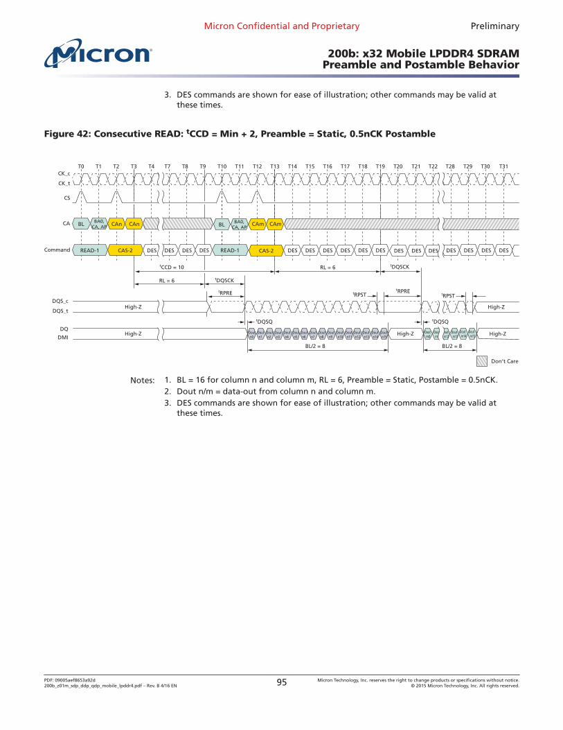
3. DES commands are shown for ease of illustration; other commands may be valid atthese times.
Figure 42: Consecutive READ: tCCD = Min + 2, Preamble = Static, 0.5nCK Postamble
T0
CK_t
CK_cT1 T2 T3 T4 T7 T20T8 T13T9 T10 T11 T12 T15 T16 T17 T18 T19
CS
T14
CA BL
Command READ-1
BA0,CA, AP CAn
CAS-2
CAn CAm CAm
RL = 6
RL = 6
BL/2 = 8
DES DES DES DES DES DES DES DES DES DES DES
tRPREtRPRE
tDQSCK
tDQSCKtCCD = 10
tRPST
tDQSQ
DQS_t
DQS_c
Don’t Care
tDQSQ
T21 T22 T31T28 T29 T30
DES DES DES DESCAS-2
Doutn0
Doutn1
Doutn2
Doutn4
Doutn6
Doutn7
Doutn8
Doutn9
Doutn10
Doutn5
Doutn12
Doutm0
Doutn13
Doutn14
Doutn15
Doutn3
Doutm1
Doutm12
Doutm14
Doutm15
Doutm13
Doutn11
High-Z
High-Z
High-Z High-Z
tRPST
BL BA0,CA, AP
READ-1
High-Z
BL/2 = 8
DES DES
DQ
DMI
Notes: 1. BL = 16 for column n and column m, RL = 6, Preamble = Static, Postamble = 0.5nCK.2. Dout n/m = data-out from column n and column m.3. DES commands are shown for ease of illustration; other commands may be valid at
these times.
Micron Confidential and Proprietary Preliminary
200b: x32 Mobile LPDDR4 SDRAMPreamble and Postamble Behavior
PDF: 09005aef8653a92d200b_z01m_sdp_ddp_qdp_mobile_lpddr4.pdf – Rev. B 4/16 EN 95 Micron Technology, Inc. reserves the right to change products or specifications without notice.
© 2015 Micron Technology, Inc. All rights reserved.
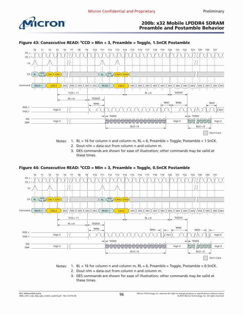
Figure 43: Consecutive READ: tCCD = Min + 3, Preamble = Toggle, 1.5nCK Postamble
T0
CK_t
CK_cT1 T2 T3 T4 T7 T20T8 T13T9 T10 T11 T12 T15 T16 T17 T18 T19
CS
T14
CA BL
Command READ-1
BA0,CA, AP CAn
CAS-2
CAn CAm CAm
RL = 6
RL = 6
BL/2 = 8
DES DES DES DES DES DES DES DES DES DES DES
tRPREtRPRE
tDQSCK
tDQSCKtCCD = 11
tRPST
DQS_t
DQS_c
Don’t Care
tDQSQ
T21 T22 T31T23 T29 T30
DES DES DESCAS-2
Doutn0
Doutn1
Doutn2
Doutn4
Doutn6
Doutn7
Doutn8
Doutn9
Doutn10
Doutn5
Doutn12
Doutn13
Doutn14
Doutn15
Doutn3
Doutn11
High-Z
High-Z
High-Z
tRPST
BL BA0,CA, AP
READ-1
High-Z
tDQSQ
Doutm0
Doutm1
Doutm12
Doutm14
Doutm15
Doutm13 High-Z
BL/2 = 8
DES DES DESDES
DQ
DMI
Notes: 1. BL = 16 for column n and column m, RL = 6, Preamble = Toggle, Postamble = 1.5nCK.2. Dout n/m = data-out from column n and column m.3. DES commands are shown for ease of illustration; other commands may be valid at
these times.
Figure 44: Consecutive READ: tCCD = Min + 3, Preamble = Toggle, 0.5nCK Postamble
T0
CK_t
CK_cT1 T2 T3 T4 T7 T20T8 T13T9 T10 T11 T12 T15 T16 T17 T18 T19
CS
T14
CA BL
Command READ-1
BA0,CA, AP CAn
CAS-2
CAn CAm CAm
RL = 6
RL = 6
BL/2 = 8
DES DES DES DES DES DES DES DES DES DES DES
tRPREtRPRE
tDQSCK
tDQSCKtCCD = 11
tRPST
DQS_t
DQS_c
Don’t Care
tDQSQ
T21 T22 T31T23 T29 T30
DES DES DESCAS-2
Doutn0
Doutn1
Doutn2
Doutn4
Doutn6
Doutn7
Doutn8
Doutn9
Doutn10
Doutn5
Doutn12
Doutn13
Doutn14
Doutn15
Doutn3
Doutn11
High-Z High-Z
tRPST
BL BA0,CA, AP
READ-1
High-Z
tDQSQ
Doutm0
Doutm1
Doutm12
Doutm14
Doutm15
Doutm13 High-Z
High-Z
BL/2 = 8
DES DES DES
High-Z
DES
DQ
DMI
Notes: 1. BL = 16 for column n and column m, RL = 6, Preamble = Toggle, Postamble = 0.5nCK.2. Dout n/m = data-out from column n and column m.3. DES commands are shown for ease of illustration; other commands may be valid at
these times.
Micron Confidential and Proprietary Preliminary
200b: x32 Mobile LPDDR4 SDRAMPreamble and Postamble Behavior
PDF: 09005aef8653a92d200b_z01m_sdp_ddp_qdp_mobile_lpddr4.pdf – Rev. B 4/16 EN 96 Micron Technology, Inc. reserves the right to change products or specifications without notice.
© 2015 Micron Technology, Inc. All rights reserved.
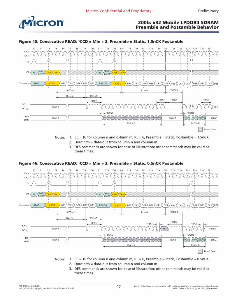
Figure 45: Consecutive READ: tCCD = Min + 3, Preamble = Static, 1.5nCK Postamble
T0
CK_t
CK_cT1 T2 T3 T4 T7 T20T8 T13T9 T10 T11 T12 T15 T16 T17 T18 T19
CS
T14
CA BL
Command READ-1
BA0,CA, AP CAn
CAS-2
CAn CAm CAm
RL = 6
RL = 6
BL/2 = 8
DES DES DES DES DES DES DES DES DES DES DES
tRPREtRPRE
tDQSCK
tDQSCKtCCD = 11
tRPST
DQS_t
DQS_c
Don’t Care
tDQSQ
T21 T22 T31T23 T29 T30
DES DES DESCAS-2
Doutn0
Doutn1
Doutn2
Doutn4
Doutn6
Doutn7
Doutn8
Doutn9
Doutn10
Doutn5
Doutn12
Doutn13
Doutn14
Doutn15
Doutn3
Doutn11
High-Z High-Z
tRPST
BL BA0,CA, AP
READ-1
High-Z
tDQSQ
Doutm0
Doutm1
Doutm12
Doutm14
Doutm15
Doutm13 High-Z
High-Z
BL/2 = 8
DES DES DESDES
DQ
DMI
Notes: 1. BL = 16 for column n and column m, RL = 6, Preamble = Static, Postamble = 1.5nCK.2. Dout n/m = data-out from column n and column m.3. DES commands are shown for ease of illustration; other commands may be valid at
these times.
Figure 46: Consecutive READ: tCCD = Min + 3, Preamble = Static, 0.5nCK Postamble
T0
CK_t
CK_cT1 T2 T3 T4 T7 T20T8 T13T9 T10 T11 T12 T15 T16 T17 T18 T19
CS
T14
CA BL
Command READ-1
BA0,CA, AP CAn
CAS-2
CAn CAm CAm
RL = 6
RL = 6
BL/2 = 8
DES DES DES DES DES DES DES DES DES DES DES
tRPREtRPRE
tDQSCK
tDQSCKtCCD = 11
tRPST
DQS_t
DQS_c
Don’t Care
tDQSQ
T21 T22 T31T23 T29 T30
DES DES DESCAS-2
Doutn0
Doutn1
Doutn2
Doutn4
Doutn6
Doutn7
Doutn8
Doutn9
Doutn10
Doutn5
Doutn12
Doutn13
Doutn14
Doutn15
Doutn3
Doutn11
High-Z High-Z
tRPST
BL BA0,CA, AP
READ-1
High-Z
tDQSQ
Doutm0
Doutm1
Doutm12
Doutm14
Doutm15
Doutm13 High-Z
High-Z
BL/2 = 8
DES DES DESDES
High-Z
DQ
DMI
Notes: 1. BL = 16 for column n and column m, RL = 6, Preamble = Static, Postamble = 0.5nCK.2. Dout n/m = data-out from column n and column m.3. DES commands are shown for ease of illustration; other commands may be valid at
these times.
Micron Confidential and Proprietary Preliminary
200b: x32 Mobile LPDDR4 SDRAMPreamble and Postamble Behavior
PDF: 09005aef8653a92d200b_z01m_sdp_ddp_qdp_mobile_lpddr4.pdf – Rev. B 4/16 EN 97 Micron Technology, Inc. reserves the right to change products or specifications without notice.
© 2015 Micron Technology, Inc. All rights reserved.
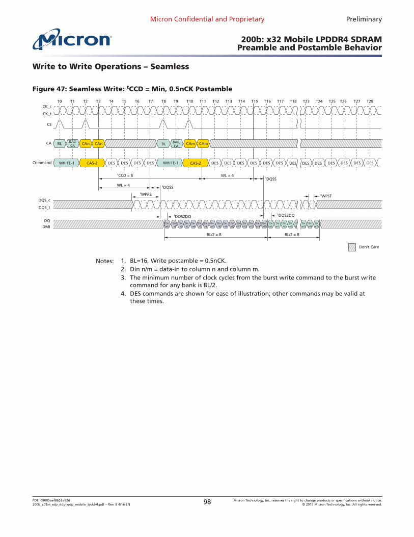
Write to Write Operations – Seamless
Figure 47: Seamless Write: tCCD = Min, 0.5nCK Postamble
T0
CK_t
CK_cT1 T2 T3 T4 T5 T24T6 T7 T8 T13T9 T10 T11 T12 T15 T16 T17 T18 T23
CS
T14
CA BL
Command WRITE-1
BA0,CA CAn
CAS-2
CAn CAm CAm
WL = 4
WL = 4
DES DES DES DES DES DES DES DES DES DES DES
tWPRE
tDQSS
tDQSStCCD = 8
tWPST
tDQS2DQ
DQS_t
DQS_c
Don’t Care
tDQS2DQ
T26T25 T27 T28
DES DES DES DESCAS-2
Dinn0
Dinn1
Dinn2
Dinn4
Dinn6
Dinn7
Dinn8
Dinn9
Dinn10
Dinn5
Dinn12
Dinm0
Dinn13
Dinn14
Dinn15
Dinn3
Dinm1
Dinm12
Dinm14
Dinm15
Dinm13
Dinm2
Dinm3
Dinn11
BL BA0,CA
WRITE-1
BL/2 = 8 BL/2 = 8
DES DES
DQ
DMI
Notes: 1. BL=16, Write postamble = 0.5nCK.2. Din n/m = data-in to column n and column m.3. The minimum number of clock cycles from the burst write command to the burst write
command for any bank is BL/2.4. DES commands are shown for ease of illustration; other commands may be valid at
these times.
Micron Confidential and Proprietary Preliminary
200b: x32 Mobile LPDDR4 SDRAMPreamble and Postamble Behavior
PDF: 09005aef8653a92d200b_z01m_sdp_ddp_qdp_mobile_lpddr4.pdf – Rev. B 4/16 EN 98 Micron Technology, Inc. reserves the right to change products or specifications without notice.
© 2015 Micron Technology, Inc. All rights reserved.
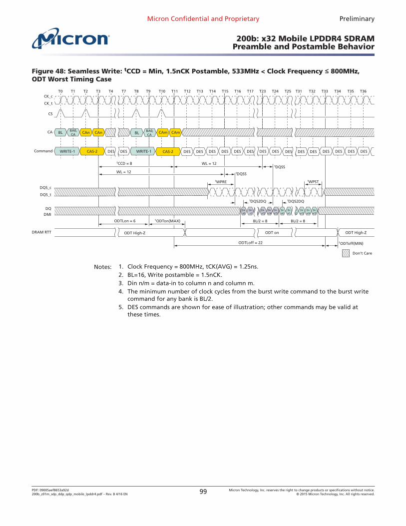
Figure 48: Seamless Write: tCCD = Min, 1.5nCK Postamble, 533MHz < Clock Frequency ≤≤ 800MHz,ODT Worst Timing Case
T0
CK_t
CK_cT1 T2 T3 T4 T24T7 T8 T13T9 T10 T11 T12 T15 T16 T17 T34T23
CS
T14
CA BL
Command WRITE-1
BA0,CA CAn
CAS-2
CAn CAm CAm
WL = 12
WL = 12
DES DES DES DESDES DES DES DES DES DES DES
tWPRE
tDQSS
tDQSStCCD = 8
tWPST
tDQS2DQ
DQS_t
DQS_c
Don’t Care
tDQS2DQ
T31T25 T32 T33 T35 T36
DES DES DES DESCAS-2
Dinn0
Dinn1
Dinn2
Dinm0
Dinn13
Dinn14
Dinn15
Dinm1
Dinm14
Dinm15
Dinm13
Dinm2
BL BA0,CA
WRITE-1
DRAM RTT
BL/2 = 8 BL/2 = 8
DES DES
ODTLon = 6
ODT High-Z ODT High-ZODT on
ODTLoff = 22
ODTon(MAX)t
ODToff(MIN)t
DQ
DMI
Notes: 1. Clock Frequency = 800MHz, tCK(AVG) = 1.25ns.2. BL=16, Write postamble = 1.5nCK.3. Din n/m = data-in to column n and column m.4. The minimum number of clock cycles from the burst write command to the burst write
command for any bank is BL/2.5. DES commands are shown for ease of illustration; other commands may be valid at
these times.
Micron Confidential and Proprietary Preliminary
200b: x32 Mobile LPDDR4 SDRAMPreamble and Postamble Behavior
PDF: 09005aef8653a92d200b_z01m_sdp_ddp_qdp_mobile_lpddr4.pdf – Rev. B 4/16 EN 99 Micron Technology, Inc. reserves the right to change products or specifications without notice.
© 2015 Micron Technology, Inc. All rights reserved.
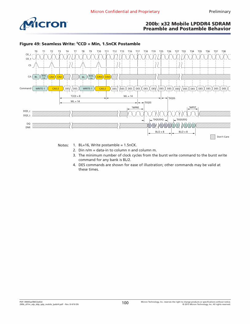
Figure 49: Seamless Write: tCCD = Min, 1.5nCK Postamble
T0
CK_t
CK_cT1 T2 T3 T4 T26T7 T8 T18T9 T10 T11 T12 T15 T16 T17 T36T25
CS
T19
CA BL
Command WRITE-1
BA0,CA CAn
CAS-2
CAn CAm CAm
WL = 14
WL = 14
DES DES DES DESDES DES DES DES DES DES DES
tWPRE
tDQSS
tDQSStCCD = 8
tWPST
tDQS2DQ
DQS_t
DQS_c
Don’t Care
tDQS2DQ
T33T27 T34 T35 T37 T38
DES DES DES DESCAS-2
Dinn0
Dinn1
Dinn2
Dinm0
Dinn13
Dinn14
Dinn15
Dinm1
Dinm14
Dinm15
Dinm13
Dinm2
BL BA0,CA
WRITE-1
BL/2 = 8 BL/2 = 8
DES DES
DQ
DMI
Notes: 1. BL=16, Write postamble = 1.5nCK.2. Din n/m = data-in to column n and column m.3. The minimum number of clock cycles from the burst write command to the burst write
command for any bank is BL/2.4. DES commands are shown for ease of illustration; other commands may be valid at
these times.
Micron Confidential and Proprietary Preliminary
200b: x32 Mobile LPDDR4 SDRAMPreamble and Postamble Behavior
PDF: 09005aef8653a92d200b_z01m_sdp_ddp_qdp_mobile_lpddr4.pdf – Rev. B 4/16 EN 100 Micron Technology, Inc. reserves the right to change products or specifications without notice.
© 2015 Micron Technology, Inc. All rights reserved.
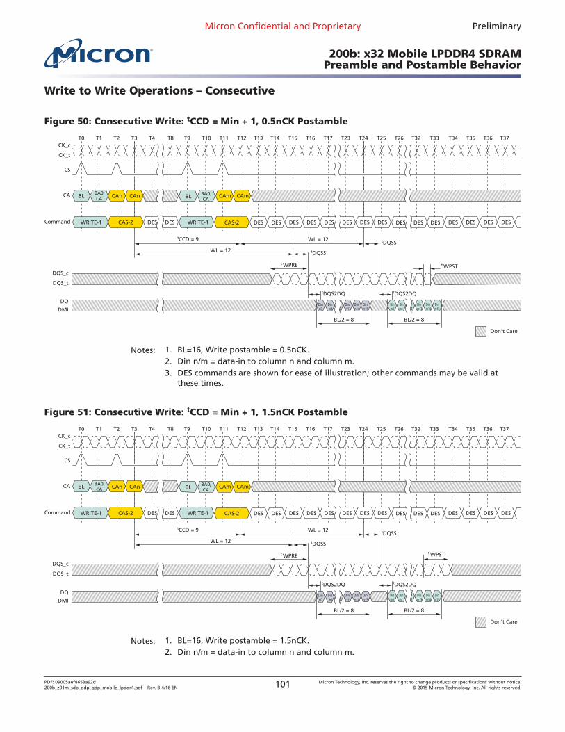
Write to Write Operations – Consecutive
Figure 50: Consecutive Write: tCCD = Min + 1, 0.5nCK Postamble
T0
CK_t
CK_cT1 T2 T3 T4 T26T23T8 T24T9 T10 T11 T12 T15 T16 T17 T36T25
CS
T14T13
CA BL
Command WRITE-1
BA0,CA CAn
CAS-2
CAn CAm CAm
WL = 12
WL = 12
DES DES DES DESDES DES DES DES DES DES DES
t WPRE
tDQSS
tDQSStCCD = 9
t WPST
DQS_t
DQS_c
Don’t Care
tDQS2DQ
T33T32 T34 T35 T37
DES DES DES DESCAS-2
Dinn0
Dinn1
Dinn2
Dinn13
Dinn14
Dinn15
BL BA0,CA
WRITE-1
BL/2 = 8
DES DES
tDQS2DQ
Dinm0
Dinm1
Dinm14
Dinm15
Dinm13
Dinm2
BL/2 = 8
DQ
DMI
Notes: 1. BL=16, Write postamble = 0.5nCK.2. Din n/m = data-in to column n and column m.3. DES commands are shown for ease of illustration; other commands may be valid at
these times.
Figure 51: Consecutive Write: tCCD = Min + 1, 1.5nCK Postamble
T0
CK_t
CK_cT1 T2 T3 T4 T26T23T8 T24T9 T10 T11 T12 T15 T16 T17 T36T25
CS
T14T13
CA BL
Command WRITE-1
BA0,CA CAn
CAS-2
CAn CAm CAm
WL = 12
WL = 12
DES DES DES DESDES DES DES DES DES DES DES
t WPRE
tDQSS
tDQSStCCD = 9
t WPST
DQS_t
DQS_c
Don’t Care
tDQS2DQ
T33T32 T34 T35 T37
DES DES DES DESCAS-2
Dinn0
Dinn1
Dinn2
Dinn13
Dinn14
Dinn15
BL BA0,CA
WRITE-1
BL/2 = 8
DES DES
tDQS2DQ
Dinm0
Dinm1
Dinm14
Dinm15
Dinm13
Dinm2
BL/2 = 8
DQ
DMI
Notes: 1. BL=16, Write postamble = 1.5nCK.2. Din n/m = data-in to column n and column m.
Micron Confidential and Proprietary Preliminary
200b: x32 Mobile LPDDR4 SDRAMPreamble and Postamble Behavior
PDF: 09005aef8653a92d200b_z01m_sdp_ddp_qdp_mobile_lpddr4.pdf – Rev. B 4/16 EN 101 Micron Technology, Inc. reserves the right to change products or specifications without notice.
© 2015 Micron Technology, Inc. All rights reserved.
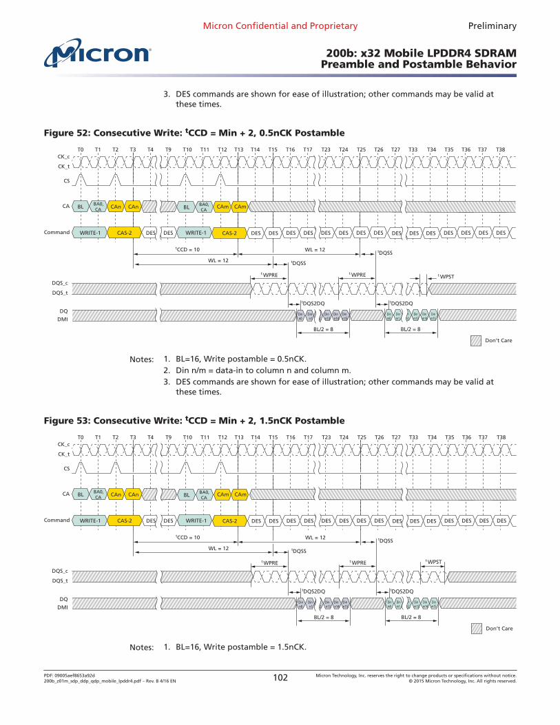
3. DES commands are shown for ease of illustration; other commands may be valid atthese times.
Figure 52: Consecutive Write: tCCD = Min + 2, 0.5nCK Postamble
T0
CK_t
CK_cT1 T2 T3 T4 T26T23 T27T24T9 T10 T11 T12 T15 T16 T17 T36T25
CS
T14T13
CA BL
Command WRITE-1
BA0,CA CAn
CAS-2
CAn CAm CAm
WL = 12
WL = 12
DES DES DES DESDES DES DES DES DES DES DES
t WPRE
tDQSS
tDQSStCCD = 10
DQS_t
DQS_c
Don’t Care
t WPRE
tDQS2DQ
T33 T38T34 T35 T37
DES DES DES DESCAS-2
Dinn0
Dinn1
Dinn2
Dinn13
Dinn14
Dinn15
BL BA0,CA
WRITE-1
BL/2 = 8
DES DES
t WPST
tDQS2DQ
Dinm0
Dinm1
Dinm14
Dinm15
Dinm13
Dinm2
BL/2 = 8
DQ
DMI
Notes: 1. BL=16, Write postamble = 0.5nCK.2. Din n/m = data-in to column n and column m.3. DES commands are shown for ease of illustration; other commands may be valid at
these times.
Figure 53: Consecutive Write: tCCD = Min + 2, 1.5nCK Postamble
T0
CK_t
CK_cT1 T2 T3 T4 T26T23 T27T24T9 T10 T11 T12 T15 T16 T17 T36T25
CS
T14T13
CA BL
Command WRITE-1
BA0,CA CAn
CAS-2
CAn CAm CAm
WL = 12
WL = 12
DES DES DES DESDES DES DES DES DES DES DES
t WPRE
tDQSS
tDQSStCCD = 10
DQS_t
DQS_c
Don’t Care
t WPRE
tDQS2DQ
T33 T38T34 T35 T37
DES DES DES DESCAS-2
Dinn0
Dinn1
Dinn2
Dinn13
Dinn14
Dinn15
BL BA0,CA
WRITE-1
BL/2 = 8
DES DES
t WPST
tDQS2DQ
Dinm0
Dinm1
Dinm14
Dinm15
Dinm13
Dinm2
BL/2 = 8
DQ
DMI
Notes: 1. BL=16, Write postamble = 1.5nCK.
Micron Confidential and Proprietary Preliminary
200b: x32 Mobile LPDDR4 SDRAMPreamble and Postamble Behavior
PDF: 09005aef8653a92d200b_z01m_sdp_ddp_qdp_mobile_lpddr4.pdf – Rev. B 4/16 EN 102 Micron Technology, Inc. reserves the right to change products or specifications without notice.
© 2015 Micron Technology, Inc. All rights reserved.
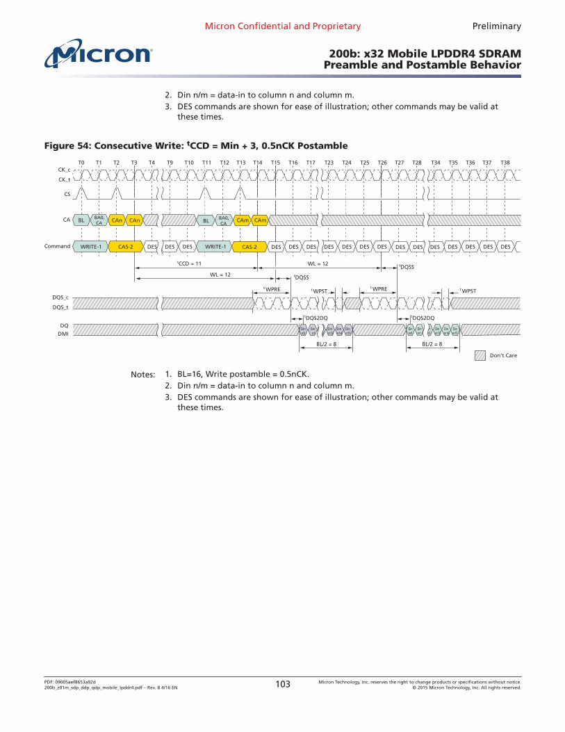
2. Din n/m = data-in to column n and column m.3. DES commands are shown for ease of illustration; other commands may be valid at
these times.
Figure 54: Consecutive Write: tCCD = Min + 3, 0.5nCK Postamble
T0
CK_t
CK_cT1 T2 T3 T4 T26T23 T27T24T9 T10 T11 T12 T15 T16 T17 T36T25
CS
T14T13
CA BL
Command WRITE-1
BA0,CA CAn
CAS-2
CAn CAm CAm
WL = 12
WL = 12
DES DES DES DES DESDES DES DES DES DES DES
t WPRE t WPRE
tDQSS
tDQSStCCD = 11
DQS_t
DQS_c
Don’t Care
tDQS2DQ
T28 T38T34 T35 T37
DES DES DES DESCAS-2
Dinn0
Dinn1
Dinn2
Dinn13
Dinn14
Dinn15
BL BA0,CA
WRITE-1
BL/2 = 8
DES DES
t WPST t WPST
tDQS2DQ
Dinm0
Dinm1
Dinm14
Dinm15
Dinm13
Dinm2
BL/2 = 8
DQ
DMI
Notes: 1. BL=16, Write postamble = 0.5nCK.2. Din n/m = data-in to column n and column m.3. DES commands are shown for ease of illustration; other commands may be valid at
these times.
Micron Confidential and Proprietary Preliminary
200b: x32 Mobile LPDDR4 SDRAMPreamble and Postamble Behavior
PDF: 09005aef8653a92d200b_z01m_sdp_ddp_qdp_mobile_lpddr4.pdf – Rev. B 4/16 EN 103 Micron Technology, Inc. reserves the right to change products or specifications without notice.
© 2015 Micron Technology, Inc. All rights reserved.
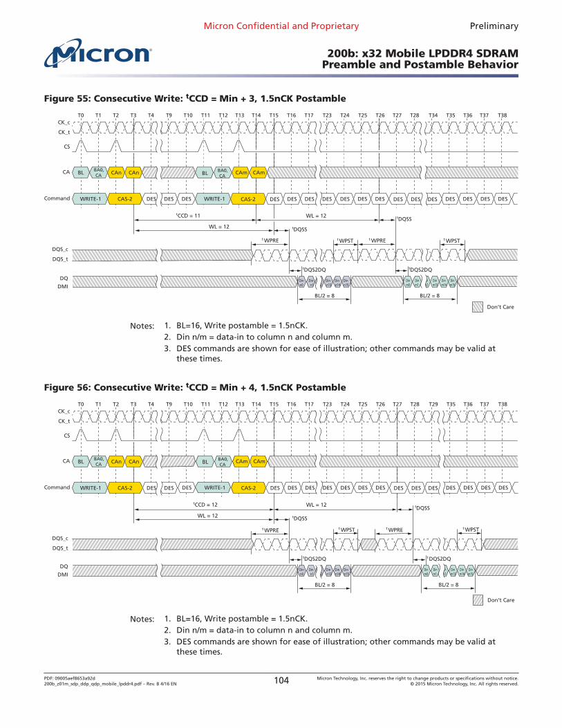
Figure 55: Consecutive Write: tCCD = Min + 3, 1.5nCK Postamble
T0
CK_t
CK_cT1 T2 T3 T4 T26T23 T27T24T9 T10 T11 T12 T15 T16 T17 T36T25
CS
T14T13
CA BL
Command WRITE-1
BA0,CA CAn
CAS-2
CAn
WL = 12
WL = 12
DES DES
t WPRE t WPRE
tDQSS
tDQSStCCD = 11
DQS_t
DQS_c
Don’t Care
tDQS2DQ
T28 T38T34 T35 T37
Dinn0
Dinn1
Dinn2
Dinn13
Dinn14
Dinn15
BL/2 = 8
t WPST
tDQS2DQ
Dinm0
Dinm1
Dinm14
Dinm15
Dinm13
Dinm2
BL/2 = 8
t WPST
CAm CAm
DES DES DESDES DES DES DES DES DES DES DES DES DESCAS-2
BL BA0,CA
WRITE-1 DES DES
DQ
DMI
Notes: 1. BL=16, Write postamble = 1.5nCK.2. Din n/m = data-in to column n and column m.3. DES commands are shown for ease of illustration; other commands may be valid at
these times.
Figure 56: Consecutive Write: tCCD = Min + 4, 1.5nCK Postamble
T0
CK_t
CK_cT1 T2 T3 T4 T26T23 T27T24T9 T10 T11 T12 T15 T16 T17 T36T25
CS
T14T13
CA BL
Command WRITE-1
BA0,CA CAn
CAS-2
CAn
WL = 12
WL = 12
DES DES
t WPRE t WPRE
tDQSS
tDQSStCCD = 12
DQS_t
DQS_c
Don’t Care
tDQS2DQ
T28 T38T29 T35 T37
Dinn0
Dinn1
Dinn2
Dinn13
Dinn14
Dinn15
BL/2 = 8
t WPST t WPST
t DQS2DQ
Dinm0
Dinm1
Dinm14
Dinm15
Dinm13
Dinm2
BL/2 = 8
CAm CAm
DES DES DESDES DES DES DES DES DES DES DES DES DESCAS-2
BL BA0,CA
WRITE-1 DES DES
DQ
DMI
Notes: 1. BL=16, Write postamble = 1.5nCK.2. Din n/m = data-in to column n and column m.3. DES commands are shown for ease of illustration; other commands may be valid at
these times.
Micron Confidential and Proprietary Preliminary
200b: x32 Mobile LPDDR4 SDRAMPreamble and Postamble Behavior
PDF: 09005aef8653a92d200b_z01m_sdp_ddp_qdp_mobile_lpddr4.pdf – Rev. B 4/16 EN 104 Micron Technology, Inc. reserves the right to change products or specifications without notice.
© 2015 Micron Technology, Inc. All rights reserved.
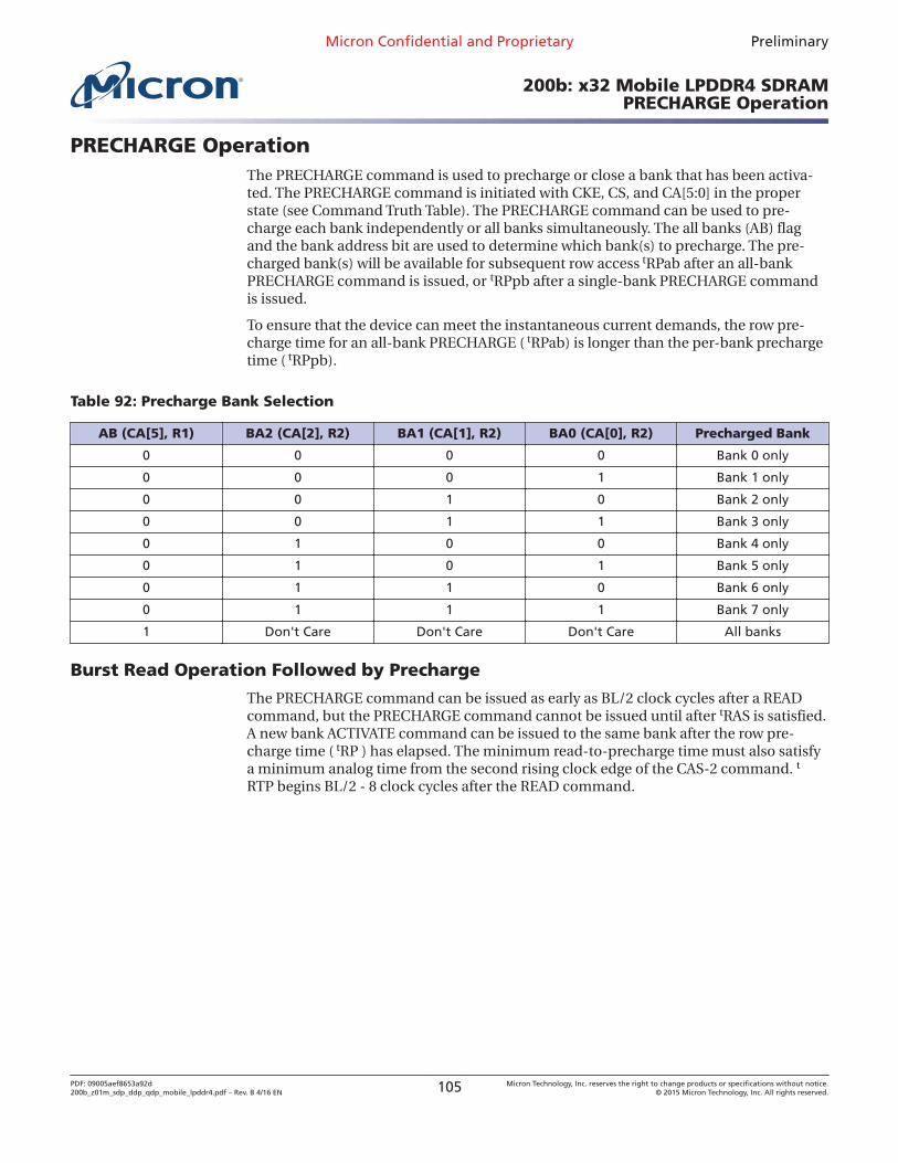
PRECHARGE OperationThe PRECHARGE command is used to precharge or close a bank that has been activa-ted. The PRECHARGE command is initiated with CKE, CS, and CA[5:0] in the properstate (see Command Truth Table). The PRECHARGE command can be used to pre-charge each bank independently or all banks simultaneously. The all banks (AB) flagand the bank address bit are used to determine which bank(s) to precharge. The pre-charged bank(s) will be available for subsequent row access tRPab after an all-bankPRECHARGE command is issued, or tRPpb after a single-bank PRECHARGE commandis issued.
To ensure that the device can meet the instantaneous current demands, the row pre-charge time for an all-bank PRECHARGE ( tRPab) is longer than the per-bank prechargetime ( tRPpb).
Table 92: Precharge Bank Selection
AB (CA[5], R1) BA2 (CA[2], R2) BA1 (CA[1], R2) BA0 (CA[0], R2) Precharged Bank
0 0 0 0 Bank 0 only
0 0 0 1 Bank 1 only
0 0 1 0 Bank 2 only
0 0 1 1 Bank 3 only
0 1 0 0 Bank 4 only
0 1 0 1 Bank 5 only
0 1 1 0 Bank 6 only
0 1 1 1 Bank 7 only
1 Don't Care Don't Care Don't Care All banks
Burst Read Operation Followed by Precharge
The PRECHARGE command can be issued as early as BL/2 clock cycles after a READcommand, but the PRECHARGE command cannot be issued until after tRAS is satisfied.A new bank ACTIVATE command can be issued to the same bank after the row pre-charge time ( tRP ) has elapsed. The minimum read-to-precharge time must also satisfya minimum analog time from the second rising clock edge of the CAS-2 command. t
RTP begins BL/2 - 8 clock cycles after the READ command.
Micron Confidential and Proprietary Preliminary
200b: x32 Mobile LPDDR4 SDRAMPRECHARGE Operation
PDF: 09005aef8653a92d200b_z01m_sdp_ddp_qdp_mobile_lpddr4.pdf – Rev. B 4/16 EN 105 Micron Technology, Inc. reserves the right to change products or specifications without notice.
© 2015 Micron Technology, Inc. All rights reserved.
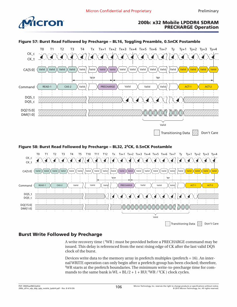
Figure 57: Burst Read Followed by Precharge – BL16, Toggling Preamble, 0.5nCK Postamble
T0 T1 T2 T3 Tx+3T4 Tx Tx+1 Tx+2 Tx+4 Tx+5 Tx+6 Ty+3Tx+7 Ty Ty+1 Ty+2 Ty+4
CA[5:0]
CK_c
CK_t
Command
Valid ValidValid Valid
READ-1
DQS_tDQS_c
DQ[15:0]DMI[1:0]
ACT-1CAS-2 Valid
Valid Valid Valid
Valid
Valid Valid ValidValid
Valid
ValidValid
Valid
tRTP
ValidValidValid
Transitioning Data
tRP
Valid
PRECHARGE ACT-2
Valid
Don’t Care
Valid
Figure 58: Burst Read Followed by Precharge – BL32, 2tCK, 0.5nCK Postamble
T0 T1 T2 T3 T12T4 T5 T10 T11 Tx+1Tx Tx+2 Tx+3 Tx+4 Tx+7Tx+5 Tx+6 Ty+3Ty Ty+1 Ty+2 Ty+4
CA[5:0]
CK_c
CK_t
Command
Valid ValidValid Valid
READ-1
DQS_tDQS_c
DQ[15:0]DMI[1:0]
ACT-1CAS-2 Valid
Valid Valid Valid
Valid
Valid Valid ValidValid
ValidValid
Valid Valid ValidValid
Valid
ValidValid
Valid
tRTP
ValidValidValid
Transitioning Data
tRP
Valid
PRECHARGE ACT-2
Valid
Don’t Care
Valid
Burst Write Followed by Precharge
A write recovery time ( tWR ) must be provided before a PRECHARGE command may beissued. This delay is referenced from the next rising edge of CK after the last valid DQSclock of the burst.
Devices write data to the memory array in prefetch multiples (prefetch = 16). An inter-nal WRITE operation can only begin after a prefetch group has been clocked; therefore,tWR starts at the prefetch boundaries. The minimum write-to-precharge time for com-mands to the same bank is WL + BL/2 + 1 + RU( tWR / tCK ) clock cycles.
Micron Confidential and Proprietary Preliminary
200b: x32 Mobile LPDDR4 SDRAMPRECHARGE Operation
PDF: 09005aef8653a92d200b_z01m_sdp_ddp_qdp_mobile_lpddr4.pdf – Rev. B 4/16 EN 106 Micron Technology, Inc. reserves the right to change products or specifications without notice.
© 2015 Micron Technology, Inc. All rights reserved.
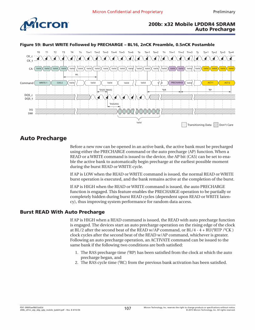
Figure 59: Burst WRITE Followed by PRECHARGE – BL16, 2nCK Preamble, 0.5nCK Postamble
T0 T1 T2 T3 T4 Tx Tx+1 Tx+3 Tx+5Tx+2 Tx+4 Tx+6 Ta Ta+2 Tn+1Ta+1 Tn Tn+2 Tn+3
CK_c
CK_t
Ty Ty+1 Ty+3Ty+2 Ty+4
CA
Command
WL
ValidValidValidValid
DQS_cDQS_t
ValidCAS-2WRITE-1
Valid
Valid
Valid Valid
Valid
Valid ValidValid
Valid
Valid Valid
Valid
Valid Valid
Valid
Valid Valid
PRECHARGE
Valid Valid
Valid
Valid Valid
ACT-1
Valid Valid ValidValid
ACT-2
Don’t CareTransitioning Data
tRP
Valid
t
t
DQSS (MAX)
DQS2DQ
tWR
DQ
DMI
Auto PrechargeBefore a new row can be opened in an active bank, the active bank must be prechargedusing either the PRECHARGE command or the auto precharge (AP) function. When aREAD or a WRITE command is issued to the device, the AP bit (CA5) can be set to ena-ble the active bank to automatically begin precharge at the earliest possible momentduring the burst READ or WRITE cycle.
If AP is LOW when the READ or WRITE command is issued, the normal READ or WRITEburst operation is executed, and the bank remains active at the completion of the burst.
If AP is HIGH when the READ or WRITE command is issued, the auto PRECHARGEfunction is engaged. This feature enables the PRECHARGE operation to be partially orcompletely hidden during burst READ cycles (dependent upon READ or WRITE laten-cy), thus improving system performance for random data access.
Burst READ With Auto Precharge
If AP is HIGH when a READ command is issued, the READ with auto precharge functionis engaged. The devices start an auto precharge operation on the rising edge of the clockat BL/2 after the second beat of the READ w/AP command, or BL/4 - 4 + RU(tRTP /tCK )clock cycles after the second beat of the READ w/AP command, whichever is greater.Following an auto precharge operation, an ACTIVATE command can be issued to thesame bank if the following two conditions are both satisfied:
1. The RAS precharge time (tRP) has been satisfied from the clock at which the autoprecharge began, and
2. The RAS cycle time (tRC) from the previous bank activation has been satisfied.
Micron Confidential and Proprietary Preliminary
200b: x32 Mobile LPDDR4 SDRAMAuto Precharge
PDF: 09005aef8653a92d200b_z01m_sdp_ddp_qdp_mobile_lpddr4.pdf – Rev. B 4/16 EN 107 Micron Technology, Inc. reserves the right to change products or specifications without notice.
© 2015 Micron Technology, Inc. All rights reserved.
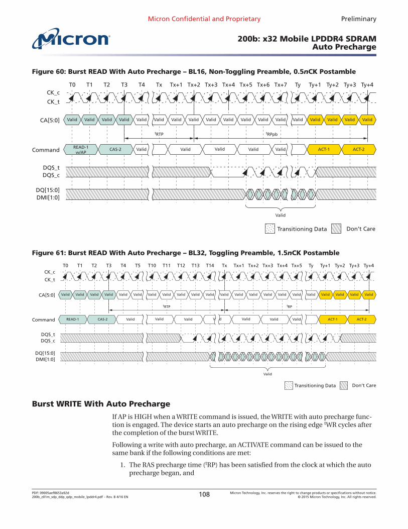
Figure 60: Burst READ With Auto Precharge – BL16, Non-Toggling Preamble, 0.5nCK Postamble
T0 T1 T2 T3 Tx+3T4 Tx Tx+1 Tx+2 Tx+4 Tx+5 Tx+6 Ty+3Tx+7 Ty Ty+1 Ty+2 Ty+4
CA[5:0]
CK_c
CK_t
Command
Valid ValidValid Valid
READ-1w/AP
DQS_tDQS_c
DQ[15:0]DMI[1:0]
ACT-1CAS-2 Valid
Valid Valid Valid
Valid
Valid Valid ValidValid
Valid
ValidValid
Valid
tRTP
ValidValidValid
Transitioning Data
tRPpb
Valid
Valid ACT-2
Valid
Don’t Care
Valid
Figure 61: Burst READ With Auto Precharge – BL32, Toggling Preamble, 1.5nCK Postamble
T0 T1 T2 T3 T12T4 T5 T10 T11 T14T13 Tx+1Tx Tx+2 Tx+3 Tx+4 Tx+5 Ty+3Ty Ty+1 Ty+2 Ty+4
CA[5:0]
CK_c
CK_t
Command
Valid ValidValid Valid
READ-1
DQS_tDQS_c
DQ[15:0]DMI[1:0]
ACT-1CAS-2 Valid
Valid Valid Valid
ValidValid
Valid Valid ValidValid
ValidValid
Valid Valid ValidValid
Valid
ValidValid
Valid
tRTP
ValidValidValid
Transitioning Data
tRP
Valid
ACT-2
Valid
Don’t Care
Valid
Burst WRITE With Auto Precharge
If AP is HIGH when a WRITE command is issued, the WRITE with auto precharge func-tion is engaged. The device starts an auto precharge on the rising edge tWR cycles afterthe completion of the burst WRITE.
Following a write with auto precharge, an ACTIVATE command can be issued to thesame bank if the following conditions are met:
1. The RAS precharge time (tRP) has been satisfied from the clock at which the autoprecharge began, and
Micron Confidential and Proprietary Preliminary
200b: x32 Mobile LPDDR4 SDRAMAuto Precharge
PDF: 09005aef8653a92d200b_z01m_sdp_ddp_qdp_mobile_lpddr4.pdf – Rev. B 4/16 EN 108 Micron Technology, Inc. reserves the right to change products or specifications without notice.
© 2015 Micron Technology, Inc. All rights reserved.
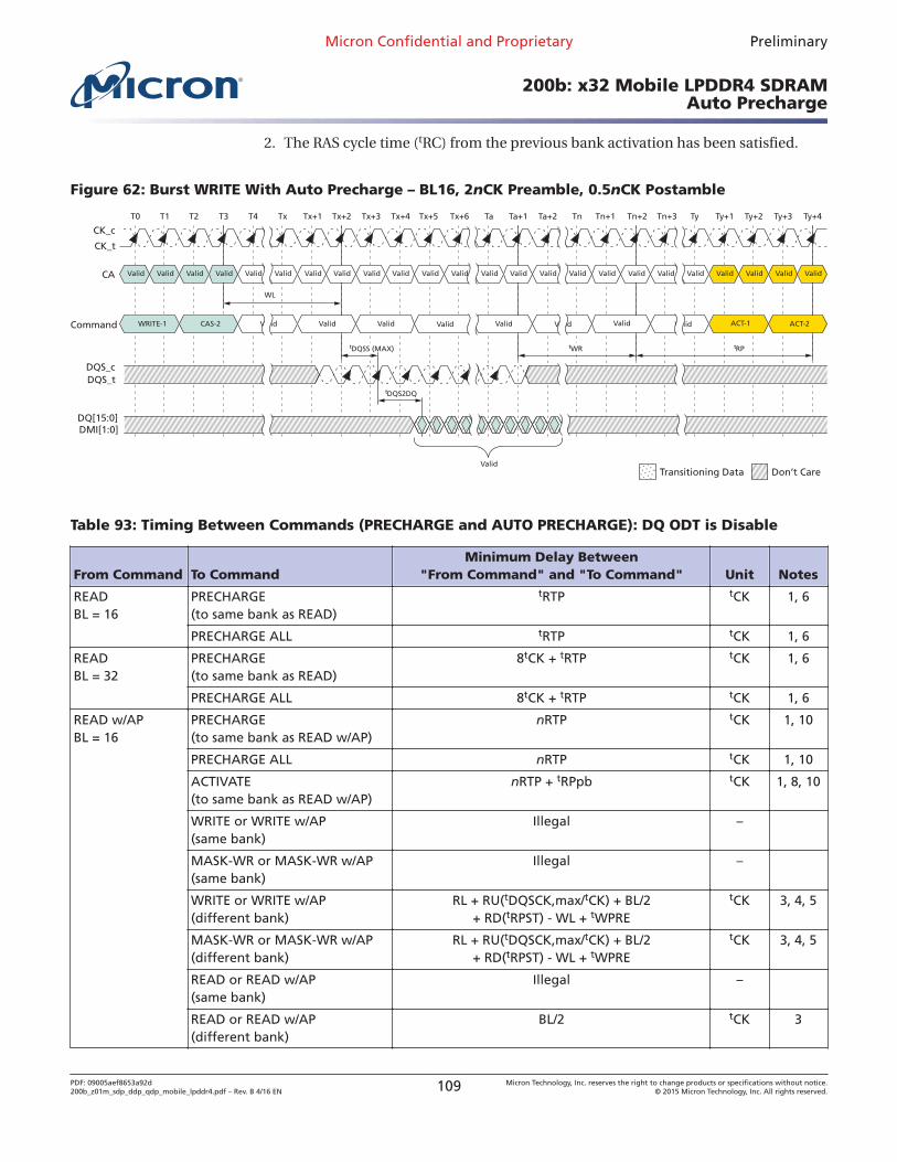
2. The RAS cycle time (tRC) from the previous bank activation has been satisfied.
Figure 62: Burst WRITE With Auto Precharge – BL16, 2nCK Preamble, 0.5nCK Postamble
T0 T1 T2 T3 T4 Tx Tx+1 Tx+3 Tx+5Tx+2 Tx+4 Tx+6 Ta Ta+2 Tn+1Ta+1 Tn Tn+2 Tn+3
CK_c
CK_t
Ty Ty+1 Ty+3Ty+2 Ty+4
CA
Command
WL
ValidValidValidValid
DQS_cDQS_t
DQ[15:0]DMI[1:0]
ValidCAS-2WRITE-1
Valid
Valid
Valid Valid
Valid
Valid ValidValid
Valid
Valid Valid
Valid
Valid Valid
Valid
Valid Valid
Valid
Valid Valid
Valid
Valid Valid
ACT-1
Valid Valid ValidValid
ACT-2
Don’t CareTransitioning Data
tRP
Valid
tDQSS (MAX)
tDQS2DQ
tWR
Table 93: Timing Between Commands (PRECHARGE and AUTO PRECHARGE): DQ ODT is Disable
From Command To CommandMinimum Delay Between
"From Command" and "To Command" Unit Notes
READBL = 16
PRECHARGE(to same bank as READ)
tRTP tCK 1, 6
PRECHARGE ALL tRTP tCK 1, 6
READBL = 32
PRECHARGE(to same bank as READ)
8tCK + tRTP tCK 1, 6
PRECHARGE ALL 8tCK + tRTP tCK 1, 6
READ w/APBL = 16
PRECHARGE(to same bank as READ w/AP)
nRTP tCK 1, 10
PRECHARGE ALL nRTP tCK 1, 10
ACTIVATE(to same bank as READ w/AP)
nRTP + tRPpb tCK 1, 8, 10
WRITE or WRITE w/AP(same bank)
Illegal –
MASK-WR or MASK-WR w/AP(same bank)
Illegal –
WRITE or WRITE w/AP(different bank)
RL + RU(tDQSCK,max/tCK) + BL/2+ RD(tRPST) - WL + tWPRE
tCK 3, 4, 5
MASK-WR or MASK-WR w/AP(different bank)
RL + RU(tDQSCK,max/tCK) + BL/2+ RD(tRPST) - WL + tWPRE
tCK 3, 4, 5
READ or READ w/AP(same bank)
Illegal –
READ or READ w/AP(different bank)
BL/2 tCK 3
Micron Confidential and Proprietary Preliminary
200b: x32 Mobile LPDDR4 SDRAMAuto Precharge
PDF: 09005aef8653a92d200b_z01m_sdp_ddp_qdp_mobile_lpddr4.pdf – Rev. B 4/16 EN 109 Micron Technology, Inc. reserves the right to change products or specifications without notice.
© 2015 Micron Technology, Inc. All rights reserved.
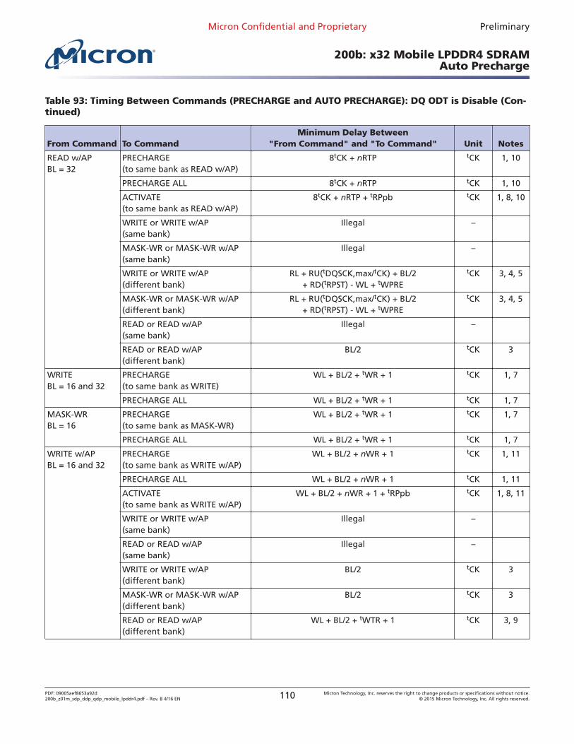
Table 93: Timing Between Commands (PRECHARGE and AUTO PRECHARGE): DQ ODT is Disable (Con-tinued)
From Command To CommandMinimum Delay Between
"From Command" and "To Command" Unit Notes
READ w/APBL = 32
PRECHARGE(to same bank as READ w/AP)
8tCK + nRTP tCK 1, 10
PRECHARGE ALL 8tCK + nRTP tCK 1, 10
ACTIVATE(to same bank as READ w/AP)
8tCK + nRTP + tRPpb tCK 1, 8, 10
WRITE or WRITE w/AP(same bank)
Illegal –
MASK-WR or MASK-WR w/AP(same bank)
Illegal –
WRITE or WRITE w/AP(different bank)
RL + RU(tDQSCK,max/tCK) + BL/2+ RD(tRPST) - WL + tWPRE
tCK 3, 4, 5
MASK-WR or MASK-WR w/AP(different bank)
RL + RU(tDQSCK,max/tCK) + BL/2+ RD(tRPST) - WL + tWPRE
tCK 3, 4, 5
READ or READ w/AP(same bank)
Illegal –
READ or READ w/AP(different bank)
BL/2 tCK 3
WRITEBL = 16 and 32
PRECHARGE(to same bank as WRITE)
WL + BL/2 + tWR + 1 tCK 1, 7
PRECHARGE ALL WL + BL/2 + tWR + 1 tCK 1, 7
MASK-WRBL = 16
PRECHARGE(to same bank as MASK-WR)
WL + BL/2 + tWR + 1 tCK 1, 7
PRECHARGE ALL WL + BL/2 + tWR + 1 tCK 1, 7
WRITE w/APBL = 16 and 32
PRECHARGE(to same bank as WRITE w/AP)
WL + BL/2 + nWR + 1 tCK 1, 11
PRECHARGE ALL WL + BL/2 + nWR + 1 tCK 1, 11
ACTIVATE(to same bank as WRITE w/AP)
WL + BL/2 + nWR + 1 + tRPpb tCK 1, 8, 11
WRITE or WRITE w/AP(same bank)
Illegal –
READ or READ w/AP(same bank)
Illegal –
WRITE or WRITE w/AP(different bank)
BL/2 tCK 3
MASK-WR or MASK-WR w/AP(different bank)
BL/2 tCK 3
READ or READ w/AP(different bank)
WL + BL/2 + tWTR + 1 tCK 3, 9
Micron Confidential and Proprietary Preliminary
200b: x32 Mobile LPDDR4 SDRAMAuto Precharge
PDF: 09005aef8653a92d200b_z01m_sdp_ddp_qdp_mobile_lpddr4.pdf – Rev. B 4/16 EN 110 Micron Technology, Inc. reserves the right to change products or specifications without notice.
© 2015 Micron Technology, Inc. All rights reserved.
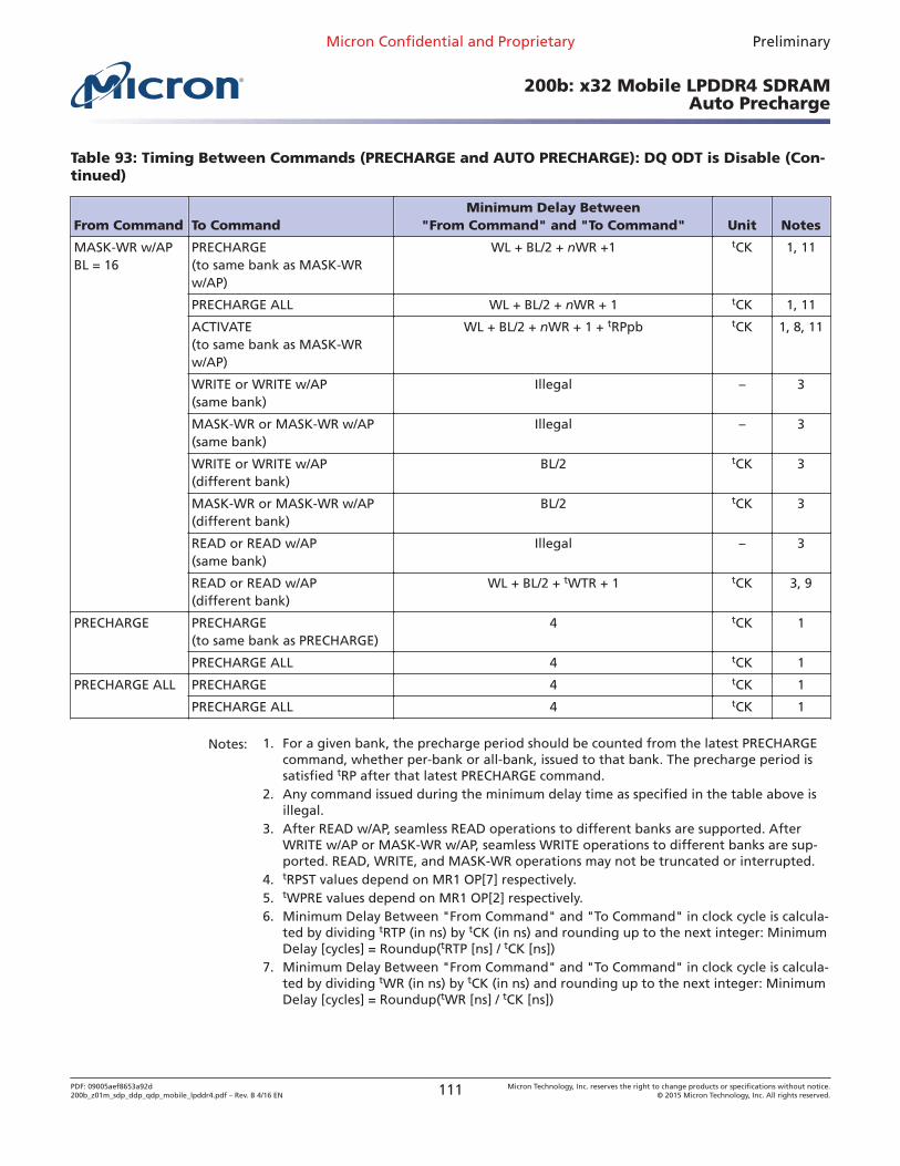
Table 93: Timing Between Commands (PRECHARGE and AUTO PRECHARGE): DQ ODT is Disable (Con-tinued)
From Command To CommandMinimum Delay Between
"From Command" and "To Command" Unit Notes
MASK-WR w/APBL = 16
PRECHARGE(to same bank as MASK-WRw/AP)
WL + BL/2 + nWR +1 tCK 1, 11
PRECHARGE ALL WL + BL/2 + nWR + 1 tCK 1, 11
ACTIVATE(to same bank as MASK-WRw/AP)
WL + BL/2 + nWR + 1 + tRPpb tCK 1, 8, 11
WRITE or WRITE w/AP(same bank)
Illegal – 3
MASK-WR or MASK-WR w/AP(same bank)
Illegal – 3
WRITE or WRITE w/AP(different bank)
BL/2 tCK 3
MASK-WR or MASK-WR w/AP(different bank)
BL/2 tCK 3
READ or READ w/AP(same bank)
Illegal – 3
READ or READ w/AP(different bank)
WL + BL/2 + tWTR + 1 tCK 3, 9
PRECHARGE PRECHARGE(to same bank as PRECHARGE)
4 tCK 1
PRECHARGE ALL 4 tCK 1
PRECHARGE ALL PRECHARGE 4 tCK 1
PRECHARGE ALL 4 tCK 1
Notes: 1. For a given bank, the precharge period should be counted from the latest PRECHARGEcommand, whether per-bank or all-bank, issued to that bank. The precharge period issatisfied tRP after that latest PRECHARGE command.
2. Any command issued during the minimum delay time as specified in the table above isillegal.
3. After READ w/AP, seamless READ operations to different banks are supported. AfterWRITE w/AP or MASK-WR w/AP, seamless WRITE operations to different banks are sup-ported. READ, WRITE, and MASK-WR operations may not be truncated or interrupted.
4. tRPST values depend on MR1 OP[7] respectively.5. tWPRE values depend on MR1 OP[2] respectively.6. Minimum Delay Between "From Command" and "To Command" in clock cycle is calcula-
ted by dividing tRTP (in ns) by tCK (in ns) and rounding up to the next integer: MinimumDelay [cycles] = Roundup(tRTP [ns] / tCK [ns])
7. Minimum Delay Between "From Command" and "To Command" in clock cycle is calcula-ted by dividing tWR (in ns) by tCK (in ns) and rounding up to the next integer: MinimumDelay [cycles] = Roundup(tWR [ns] / tCK [ns])
Micron Confidential and Proprietary Preliminary
200b: x32 Mobile LPDDR4 SDRAMAuto Precharge
PDF: 09005aef8653a92d200b_z01m_sdp_ddp_qdp_mobile_lpddr4.pdf – Rev. B 4/16 EN 111 Micron Technology, Inc. reserves the right to change products or specifications without notice.
© 2015 Micron Technology, Inc. All rights reserved.
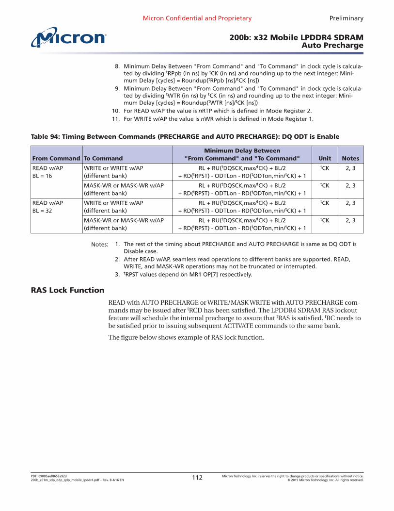
8. Minimum Delay Between "From Command" and "To Command" in clock cycle is calcula-ted by dividing tRPpb (in ns) by tCK (in ns) and rounding up to the next integer: Mini-mum Delay [cycles] = Roundup(tRPpb [ns]/tCK [ns])
9. Minimum Delay Between "From Command" and "To Command" in clock cycle is calcula-ted by dividing tWTR (in ns) by tCK (in ns) and rounding up to the next integer: Mini-mum Delay [cycles] = Roundup(tWTR [ns]/tCK [ns])
10. For READ w/AP the value is nRTP which is defined in Mode Register 2.11. For WRITE w/AP the value is nWR which is defined in Mode Register 1.
Table 94: Timing Between Commands (PRECHARGE and AUTO PRECHARGE): DQ ODT is Enable
From Command To CommandMinimum Delay Between
"From Command" and "To Command" Unit Notes
READ w/APBL = 16
WRITE or WRITE w/AP(different bank)
RL + RU(tDQSCK,max/tCK) + BL/2+ RD(tRPST) - ODTLon - RD(tODTon,min/tCK) + 1
tCK 2, 3
MASK-WR or MASK-WR w/AP(different bank)
RL + RU(tDQSCK,max/tCK) + BL/2+ RD(tRPST) - ODTLon - RD(tODTon,min/tCK) + 1
tCK 2, 3
READ w/APBL = 32
WRITE or WRITE w/AP(different bank)
RL + RU(tDQSCK,max/tCK) + BL/2+ RD(tRPST) - ODTLon - RD(tODTon,min/tCK) + 1
tCK 2, 3
MASK-WR or MASK-WR w/AP(different bank)
RL + RU(tDQSCK,max/tCK) + BL/2+ RD(tRPST) - ODTLon - RD(tODTon,min/tCK) + 1
tCK 2, 3
Notes: 1. The rest of the timing about PRECHARGE and AUTO PRECHARGE is same as DQ ODT isDisable case.
2. After READ w/AP, seamless read operations to different banks are supported. READ,WRITE, and MASK-WR operations may not be truncated or interrupted.
3. tRPST values depend on MR1 OP[7] respectively.
RAS Lock Function
READ with AUTO PRECHARGE or WRITE/MASK WRITE with AUTO PRECHARGE com-mands may be issued after tRCD has been satisfied. The LPDDR4 SDRAM RAS lockoutfeature will schedule the internal precharge to assure that tRAS is satisfied. tRC needs tobe satisfied prior to issuing subsequent ACTIVATE commands to the same bank.
The figure below shows example of RAS lock function.
Micron Confidential and Proprietary Preliminary
200b: x32 Mobile LPDDR4 SDRAMAuto Precharge
PDF: 09005aef8653a92d200b_z01m_sdp_ddp_qdp_mobile_lpddr4.pdf – Rev. B 4/16 EN 112 Micron Technology, Inc. reserves the right to change products or specifications without notice.
© 2015 Micron Technology, Inc. All rights reserved.
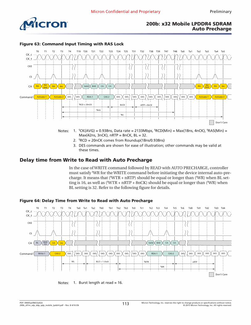
Figure 63: Command Input Timing with RAS Lock
T0 T1 T2 T3 T4 Ta0 Ta1 Ta3Ta2CK_c
CK_t
T20T19 T22 T23T21 Ta5Ta4T25T24 T32 T47 T48T31 T39T38
CA
Command
t 8nCK
tRAS
tRC
RA RA RA
DESActivate-1 Activate-2
RABA0
Valid CA CABA0
DES
RA RA RA
Activate-1 Activate-2
RABA0
RDA-1 CAS-2 DES DES DES DES DES DES DES
CS
CKE
Don’t Care
nRTP = 8nCK
DESDES DES
RCD = 20nCK
Notes: 1. tCK(AVG) = 0.938ns, Data rate = 2133Mbps, tRCD(Min) = Max(18ns, 4nCK), tRAS(Min) =Max(42ns, 3nCK), nRTP = 8nCK, BL = 32.
2. tRCD = 20nCK comes from Roundup(18ns/0.938ns)3. DES commands are shown for ease of illustration; other commands may be valid at
these times.
Delay time from Write to Read with Auto Precharge
In the case of WRITE command followed by READ with AUTO PRECHARGE, controllermust satisfy tWR for the WRITE command before initiating the device internal auto-pre-charge. It means that (tWTR + nRTP) should be equal or longer than (tWR) when BL set-ting is 16, as well as (tWTR + nRTP + 8nCK) should be equal or longer than (tWR) whenBL setting is 32. Refer to the following figure for details.
Figure 64: Delay Time from Write to Read with Auto Precharge
T0 T1 T2 T3 T4 Tc6 Td0 Td2Td1CK_c
CK_t
Ta1Ta0 Tb0 Tb1Ta2 Td4Td3Tb3Tb2 Tc1 Tc4 Tc5Tc0 Tc3Tc2
CA
Command
WL
tWR
BL CA CA
DESWrite-1 CAS-2
BA0CA Valid CA CABA0
DESRDA-1 CAS-2DES DES DESDES DES DES DES
CS
CKE
Don’t Care
nRTP
DES DESDES DES DESDES DES
BL/2 + 1 clock tWTR
Notes: 1. Burst length at read = 16.
Micron Confidential and Proprietary Preliminary
200b: x32 Mobile LPDDR4 SDRAMAuto Precharge
PDF: 09005aef8653a92d200b_z01m_sdp_ddp_qdp_mobile_lpddr4.pdf – Rev. B 4/16 EN 113 Micron Technology, Inc. reserves the right to change products or specifications without notice.
© 2015 Micron Technology, Inc. All rights reserved.
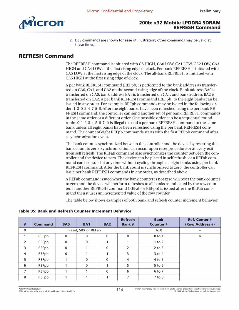
2. DES commands are shown for ease of illustration; other commands may be valid atthese times.
REFRESH CommandThe REFRESH command is initiated with CS HIGH, CA0 LOW, CA1 LOW, CA2 LOW, CA3HIGH and CA4 LOW at the first rising edge of clock. Per bank REFRESH is initiated withCA5 LOW at the first rising edge of the clock. The all-bank REFRESH is initiated withCA5 HIGH at the first rising edge of clock.
A per bank REFRESH command (REFpb) is performed to the bank address as transfer-red on CA0, CA1, and CA2 on the second rising edge of the clock. Bank address BA0 istransferred on CA0, bank address BA1 is transferred on CA1, and bank address BA2 istransferred on CA2. A per bank REFRESH command (REFpb) to the eight banks can beissued in any order. For example, REFpb commands may be issued in the following or-der: 1-3-0-2-4-7-5-6. After the eight banks have been refreshed using the per bank RE-FRESH command, the controller can send another set of per bank REFRESH commandsin the same order or a different order. One possible order can be a sequential roundrobin: 0-1-2-3-4-5-6-7. It is illegal to send a per bank REFRESH command to the samebank unless all eight banks have been refreshed using the per bank REFRESH com-mand. The count of eight REFpb commands starts with the first REFpb command aftera synchronization event.
The bank count is synchronized between the controller and the device by resetting thebank count to zero. Synchronization can occur upon reset procedure or at every exitfrom self refresh. The REFab command also synchronizes the counter between the con-troller and the device to zero. The device can be placed in self refresh, or a REFab com-mand can be issued at any time without cycling through all eight banks using per bankREFRESH command. After the bank count is synchronized to zero, the controller canissue per bank REFRESH commands in any order, as described above.
A REFab command issued when the bank counter is not zero will reset the bank counterto zero and the device will perform refreshes to all banks as indicated by the row coun-ter. If another REFRESH command (REFab or REFpb) is issued after the REFab com-mand then it uses an incremented value of the row counter.
The table below shows examples of both bank and refresh counter increment behavior.
Table 95: Bank and Refresh Counter Increment Behavior
# Command BA0 BA1 BA2RefreshBank #
BankCounter #
Ref. Conter #(Row Address #)
0 Reset, SRX or REFab To 0 –
1 REFpb 0 0 0 0 0 to 1 n
2 REFpb 0 0 1 1 1 to 2
3 REFpb 0 1 0 2 2 to 3
4 REFpb 0 1 1 3 3 to 4
5 REFpb 1 0 0 4 4 to 5
6 REFpb 1 0 1 5 5 to 6
7 REFpb 1 1 0 6 6 to 7
8 REFpb 1 1 1 7 7 to 0
Micron Confidential and Proprietary Preliminary
200b: x32 Mobile LPDDR4 SDRAMREFRESH Command
PDF: 09005aef8653a92d200b_z01m_sdp_ddp_qdp_mobile_lpddr4.pdf – Rev. B 4/16 EN 114 Micron Technology, Inc. reserves the right to change products or specifications without notice.
© 2015 Micron Technology, Inc. All rights reserved.
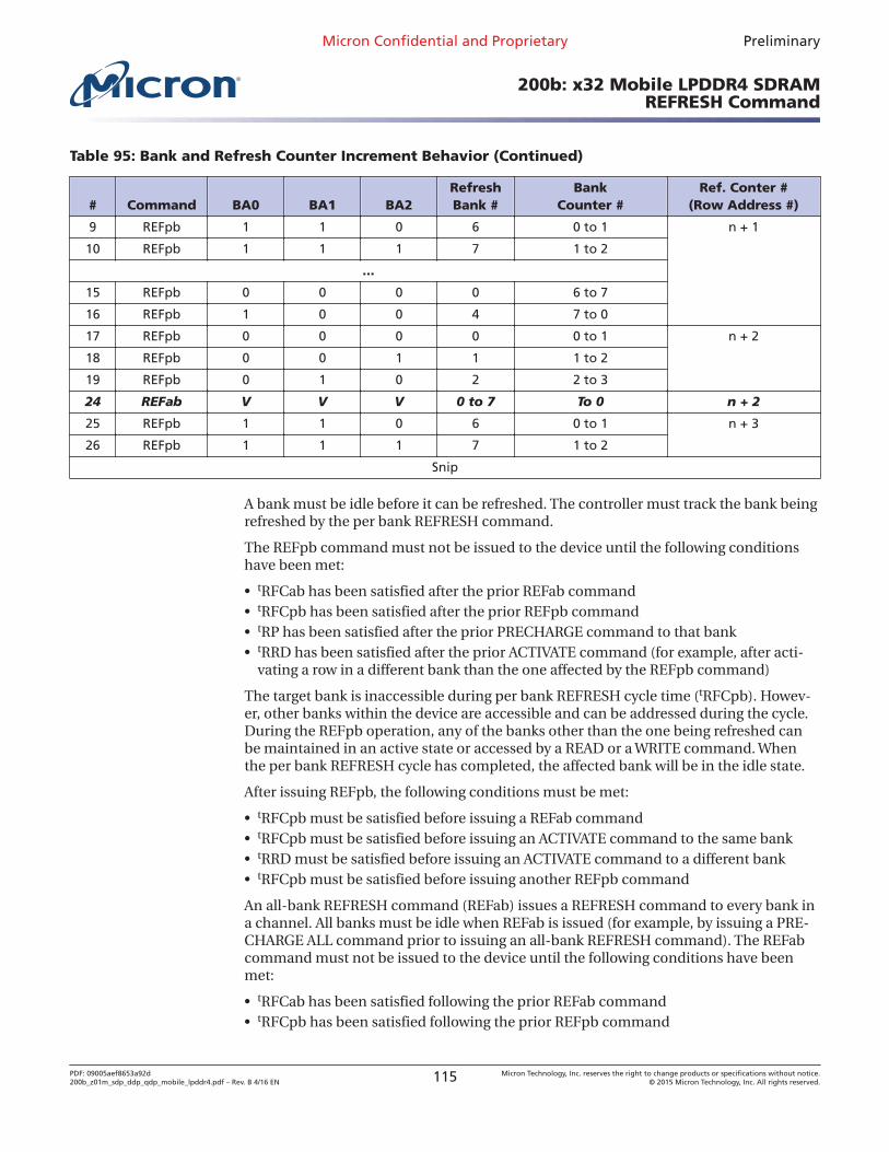
Table 95: Bank and Refresh Counter Increment Behavior (Continued)
# Command BA0 BA1 BA2RefreshBank #
BankCounter #
Ref. Conter #(Row Address #)
9 REFpb 1 1 0 6 0 to 1 n + 1
10 REFpb 1 1 1 7 1 to 2
...
15 REFpb 0 0 0 0 6 to 7
16 REFpb 1 0 0 4 7 to 0
17 REFpb 0 0 0 0 0 to 1 n + 2
18 REFpb 0 0 1 1 1 to 2
19 REFpb 0 1 0 2 2 to 3
24 REFab V V V 0 to 7 To 0 n + 2
25 REFpb 1 1 0 6 0 to 1 n + 3
26 REFpb 1 1 1 7 1 to 2
Snip
A bank must be idle before it can be refreshed. The controller must track the bank beingrefreshed by the per bank REFRESH command.
The REFpb command must not be issued to the device until the following conditionshave been met:
• tRFCab has been satisfied after the prior REFab command• tRFCpb has been satisfied after the prior REFpb command• tRP has been satisfied after the prior PRECHARGE command to that bank• tRRD has been satisfied after the prior ACTIVATE command (for example, after acti-
vating a row in a different bank than the one affected by the REFpb command)
The target bank is inaccessible during per bank REFRESH cycle time (tRFCpb). Howev-er, other banks within the device are accessible and can be addressed during the cycle.During the REFpb operation, any of the banks other than the one being refreshed canbe maintained in an active state or accessed by a READ or a WRITE command. Whenthe per bank REFRESH cycle has completed, the affected bank will be in the idle state.
After issuing REFpb, the following conditions must be met:
• tRFCpb must be satisfied before issuing a REFab command• tRFCpb must be satisfied before issuing an ACTIVATE command to the same bank• tRRD must be satisfied before issuing an ACTIVATE command to a different bank• tRFCpb must be satisfied before issuing another REFpb command
An all-bank REFRESH command (REFab) issues a REFRESH command to every bank ina channel. All banks must be idle when REFab is issued (for example, by issuing a PRE-CHARGE ALL command prior to issuing an all-bank REFRESH command). The REFabcommand must not be issued to the device until the following conditions have beenmet:
• tRFCab has been satisfied following the prior REFab command• tRFCpb has been satisfied following the prior REFpb command
Micron Confidential and Proprietary Preliminary
200b: x32 Mobile LPDDR4 SDRAMREFRESH Command
PDF: 09005aef8653a92d200b_z01m_sdp_ddp_qdp_mobile_lpddr4.pdf – Rev. B 4/16 EN 115 Micron Technology, Inc. reserves the right to change products or specifications without notice.
© 2015 Micron Technology, Inc. All rights reserved.
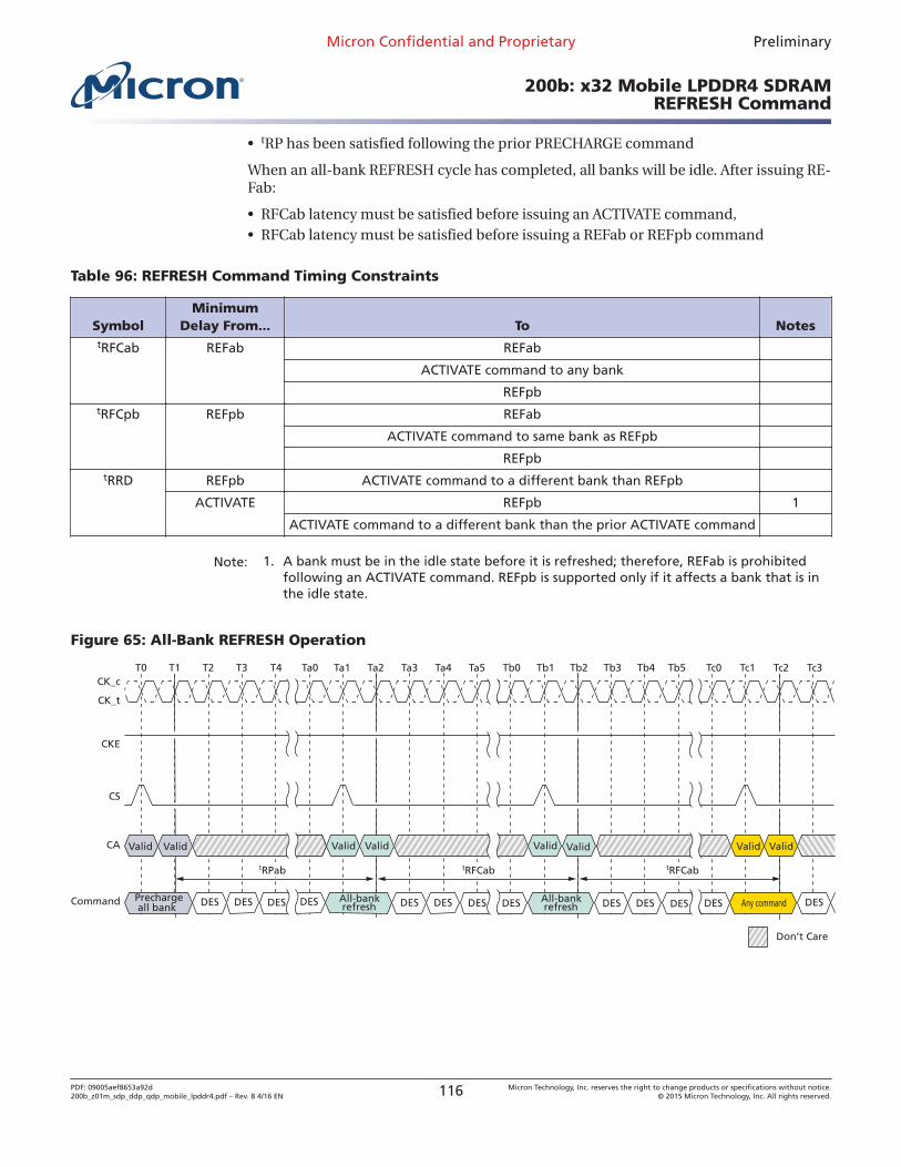
• tRP has been satisfied following the prior PRECHARGE command
When an all-bank REFRESH cycle has completed, all banks will be idle. After issuing RE-Fab:
• RFCab latency must be satisfied before issuing an ACTIVATE command,• RFCab latency must be satisfied before issuing a REFab or REFpb command
Table 96: REFRESH Command Timing Constraints
SymbolMinimum
Delay From... To NotestRFCab REFab REFab
ACTIVATE command to any bank
REFpb tRFCpb REFpb REFab
ACTIVATE command to same bank as REFpb
REFpb tRRD REFpb ACTIVATE command to a different bank than REFpb
ACTIVATE REFpb 1
ACTIVATE command to a different bank than the prior ACTIVATE command
Note: 1. A bank must be in the idle state before it is refreshed; therefore, REFab is prohibitedfollowing an ACTIVATE command. REFpb is supported only if it affects a bank that is inthe idle state.
Figure 65: All-Bank REFRESH Operation
T0 T1 T2 T3 T4 Ta0 Ta1 Ta2 Tb2Ta3 Ta4 Ta5 Tb0 Tb1 Tb4 Tb5 Tc0 Tc1 Tc2 Tc3Tb3
CK_t
CK_c
Don’t Care
CS
CKE
CA Valid
Command Precharge DESDES DES DES DESDES DES DES DESall bank
Valid Valid Valid Valid Valid
All-bankrefresh DESDES DESDES
Valid Valid
All-bankrefresh Any command
tRFCabtRFCabtRPab
Micron Confidential and Proprietary Preliminary
200b: x32 Mobile LPDDR4 SDRAMREFRESH Command
PDF: 09005aef8653a92d200b_z01m_sdp_ddp_qdp_mobile_lpddr4.pdf – Rev. B 4/16 EN 116 Micron Technology, Inc. reserves the right to change products or specifications without notice.
© 2015 Micron Technology, Inc. All rights reserved.
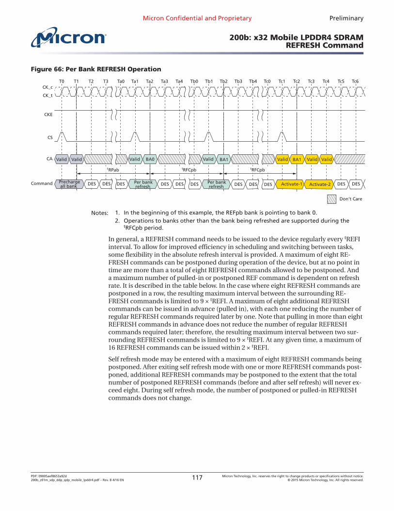
Figure 66: Per Bank REFRESH Operation
T0
CK_t
CK_cT1 T2 T3 Ta0 Ta1 Tc4Ta2 Tb2Ta3 Ta4 Tb0 Tb1 Tb4 Tc0 Tc1 Tc2 Tc3Tb3
Don’t Care
Tc5 Tc6
CS
CKE
CA Valid
Command Precharge DESDES DES DESDES DES DES DESall bank
Valid Valid BA0 Valid
Per bankrefresh
BA1
DESDES DES
Valid
Activate-1
BA1 Valid Valid
Per bankrefresh Activate-2
tRFCpbtRFCpbtRPab
Notes: 1. In the beginning of this example, the REFpb bank is pointing to bank 0.2. Operations to banks other than the bank being refreshed are supported during the
tRFCpb period.
In general, a REFRESH command needs to be issued to the device regularly every tREFIinterval. To allow for improved efficiency in scheduling and switching between tasks,some flexibility in the absolute refresh interval is provided. A maximum of eight RE-FRESH commands can be postponed during operation of the device, but at no point intime are more than a total of eight REFRESH commands allowed to be postponed. Anda maximum number of pulled-in or postponed REF command is dependent on refreshrate. It is described in the table below. In the case where eight REFRESH commands arepostponed in a row, the resulting maximum interval between the surrounding RE-FRESH commands is limited to 9 × tREFI. A maximum of eight additional REFRESHcommands can be issued in advance (pulled in), with each one reducing the number ofregular REFRESH commands required later by one. Note that pulling in more than eightREFRESH commands in advance does not reduce the number of regular REFRESHcommands required later; therefore, the resulting maximum interval between two sur-rounding REFRESH commands is limited to 9 × tREFI. At any given time, a maximum of16 REFRESH commands can be issued within 2 × tREFI.
Self refresh mode may be entered with a maximum of eight REFRESH commands beingpostponed. After exiting self refresh mode with one or more REFRESH commands post-poned, additional REFRESH commands may be postponed to the extent that the totalnumber of postponed REFRESH commands (before and after self refresh) will never ex-ceed eight. During self refresh mode, the number of postponed or pulled-in REFRESHcommands does not change.
Micron Confidential and Proprietary Preliminary
200b: x32 Mobile LPDDR4 SDRAMREFRESH Command
PDF: 09005aef8653a92d200b_z01m_sdp_ddp_qdp_mobile_lpddr4.pdf – Rev. B 4/16 EN 117 Micron Technology, Inc. reserves the right to change products or specifications without notice.
© 2015 Micron Technology, Inc. All rights reserved.
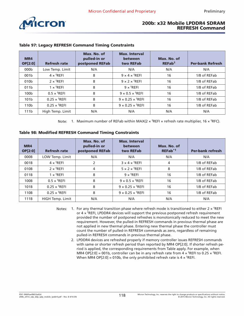
Table 97: Legacy REFRESH Command Timing Constraints
MR4OP[2:0] Refresh rate
Max. No. ofpulled-in or
postponed REFab
Max. Intervalbetween
two REFabMax. No. of
REFab1 Per-bank Refresh
000b Low Temp. Limit N/A N/A N/A N/A
001b 4 × tREFI 8 9 × 4 × tREFI 16 1/8 of REFab
010b 2 × tREFI 8 9 × 2 × tREFI 16 1/8 of REFab
011b 1 × tREFI 8 9 × tREFI 16 1/8 of REFab
100b 0.5 × tREFI 8 9 × 0.5 × tREFI 16 1/8 of REFab
101b 0.25 × tREFI 8 9 × 0.25 × tREFI 16 1/8 of REFab
110b 0.25 × tREFI 8 9 × 0.25 × tREFI 16 1/8 of REFab
111b High Temp. Limit N/A N/A N/A N/A
Note: 1. Maximum number of REFab within MAX(2 × tREFI × refresh rate multiplier, 16 × tRFC).
Table 98: Modified REFRESH Command Timing Constraints
MR4 OP[2:0] Refresh rate
Max. No. ofpulled-in or
postponed REFab
Max. Intervalbetween
two REFabMax. No. of
REFab*1 Per-bank refresh
000B LOW Temp. Limit N/A N/A N/A N/A
001B 4 × tREFI 2 3 × 4 × tREFI 4 1/8 of REFab
010B 2 × tREFI 4 5 × 2 × tREFI 8 1/8 of REFab
011B 1 × tREFI 8 9 × tREFI 16 1/8 of REFab
100B 0.5 × tREFI 8 9 × 0.5 × tREFI 16 1/8 of REFab
101B 0.25 × tREFI 8 9 × 0.25 × tREFI 16 1/8 of REFab
110B 0.25 × tREFI 8 9 × 0.25 × tREFI 16 1/8 of REFab
111B HIGH Temp. Limit N/A N/A N/A N/A
Notes: 1. For any thermal transition phase where refresh mode is transitioned to either 2 × tREFIor 4 × tREFI, LPDDR4 devices will support the previous postponed refresh requirementprovided the number of postponed refreshes is monotonically reduced to meet the newrequirement. However, the pulled-in REFRESH commands in previous thermal phase arenot applied in new thermal phase. Entering new thermal phase the controller mustcount the number of pulled-in REFRESH commands as zero, regardless of remainingpulled-in REFRESH commands in previous thermal phase.
2. LPDDR4 devices are refreshed properly if memory controller issues REFRESH commandswith same or shorter refresh period than reported by MR4 OP[2:0]. If shorter refresh pe-riod is applied, the corresponding requirements from Table apply. For example, whenMR4 OP[2:0] = 001b, controller can be in any refresh rate from 4 × tREFI to 0.25 × tREFI.When MR4 OP[2:0] = 010b, the only prohibited refresh rate is 4 × tREFI.
Micron Confidential and Proprietary Preliminary
200b: x32 Mobile LPDDR4 SDRAMREFRESH Command
PDF: 09005aef8653a92d200b_z01m_sdp_ddp_qdp_mobile_lpddr4.pdf – Rev. B 4/16 EN 118 Micron Technology, Inc. reserves the right to change products or specifications without notice.
© 2015 Micron Technology, Inc. All rights reserved.
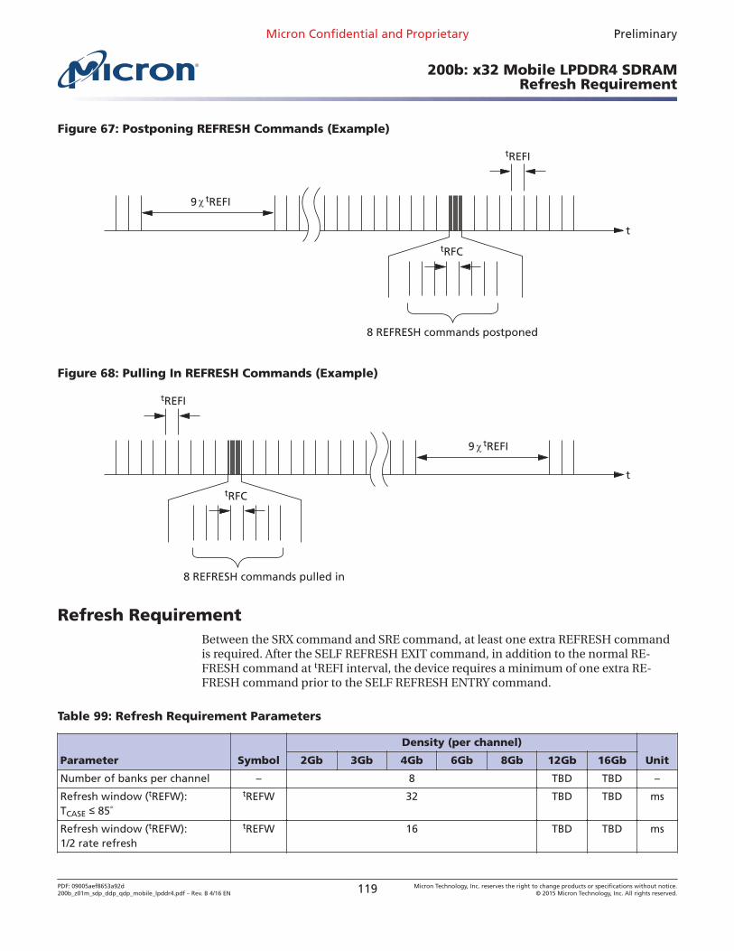
Figure 67: Postponing REFRESH Commands (Example)
9 tREFI
tREFI
8 REFRESH commands postponed
t
tRFC
Figure 68: Pulling In REFRESH Commands (Example)
9 tREFI
tREFI
8 REFRESH commands pulled in
t
tRFC
Refresh RequirementBetween the SRX command and SRE command, at least one extra REFRESH commandis required. After the SELF REFRESH EXIT command, in addition to the normal RE-FRESH command at tREFI interval, the device requires a minimum of one extra RE-FRESH command prior to the SELF REFRESH ENTRY command.
Table 99: Refresh Requirement Parameters
Parameter Symbol
Density (per channel)
Unit2Gb 3Gb 4Gb 6Gb 8Gb 12Gb 16Gb
Number of banks per channel – 8 TBD TBD –
Refresh window (tREFW):TCASE ≤ 85˚
tREFW 32 TBD TBD ms
Refresh window (tREFW):1/2 rate refresh
tREFW 16 TBD TBD ms
Micron Confidential and Proprietary Preliminary
200b: x32 Mobile LPDDR4 SDRAMRefresh Requirement
PDF: 09005aef8653a92d200b_z01m_sdp_ddp_qdp_mobile_lpddr4.pdf – Rev. B 4/16 EN 119 Micron Technology, Inc. reserves the right to change products or specifications without notice.
© 2015 Micron Technology, Inc. All rights reserved.
Table 99: Refresh Requirement Parameters (Continued)
Parameter Symbol
Density (per channel)
Unit2Gb 3Gb 4Gb 6Gb 8Gb 12Gb 16Gb
Refresh window (tREFW):1/4 rate refresh
tREFW 8 TBD TBD ms
Required number of REFRESHcommands in tREFW window
R 8192 TBD TBD –
Average refresh internal REFab tREFI 3.904 TBD TBD μs
REFpb tREFIpb 488 TBD TBD ns
REFRESH cycle time (all banks) tRFCab 130 180 280 TBD TBD ns
REFRESH cycle time (per bank) tRFCpb 60 90 140 TBD TBD ns
Notes: 1. Refresh for each channel is independent of the other channel on the die, or other chan-nels in a package. Power delivery in the user’s system should be verified to make surethe DC operating conditions are maintained when multiple channels are refreshed si-multaneously.
2. Self refresh abort feature is available for higher density devices starting with 6Gb densi-ty per channel device and tXSR_abort(min) is defined as tRFCpb + 17.5ns.
SELF REFRESH Operation
Self Refresh Entry and Exit
The SELF REFRESH command can be used to retain data in the device without externalREFRESH commands. The device has a built-in timer to accommodate SELF REFRESHoperation. Self refresh is entered by the SELF REFRESH ENTRY command defined byhaving CS HIGH, CA0 LOW, CA1 LOW, CA2 LOW, CA3 HIGH, CA4 HIGH, and CA5 valid(valid meaning that it is at a logic level HIGH or LOW) for the first rising edge, and CSLOW, CA0 valid, CA1 valid, CA2 valid, CA3 valid, CA4 valid, and CA5 valid at the secondrising edge of clock. The SELF REFRESH command is only allowed when READ DATAburst is completed and the device is in the idle state.
During self refresh mode, external clock input is needed and all input pins of the deviceare activated. The device can accept the following commands: MRR-1, CAS-2, DES, SRX,MPC, MRW-1, and MRW-2, except PASR bank/segment setting.
The device can operate in self refresh mode within the standard and elevated tempera-ture ranges. It also manages self refresh power consumption when the operating tem-perature changes: lower at low temperatures and higher at high temperatures.
For proper SELF REFRESH operation, power supply pins (VDD1, VDD2, and VDDQ) mustbe at valid levels. VDDQ can be turned off during self refresh with power-down aftertESCKE is satisfied. (Refer the figure of Power Down Entry and Exit during Self Refresh.)Prior to exiting self refresh with power-down, VDDQ must be within specified limits. Theminimum time that the device must remain in self refresh mode is tSR (MIN). Once selfrefresh exit is registered, only MRR-1, CAS-2, DES, MPC, MRW-1, and MRW-2 exceptPASR bank/segment setting are allowed until tXSR is satisfied.
The use of self refresh mode introduces the possibility that an internally timed refreshevent can be missed when self refresh exit is registered. Upon exit from self refresh, it is
Micron Confidential and Proprietary Preliminary
200b: x32 Mobile LPDDR4 SDRAMSELF REFRESH Operation
PDF: 09005aef8653a92d200b_z01m_sdp_ddp_qdp_mobile_lpddr4.pdf – Rev. B 4/16 EN 120 Micron Technology, Inc. reserves the right to change products or specifications without notice.
© 2015 Micron Technology, Inc. All rights reserved.
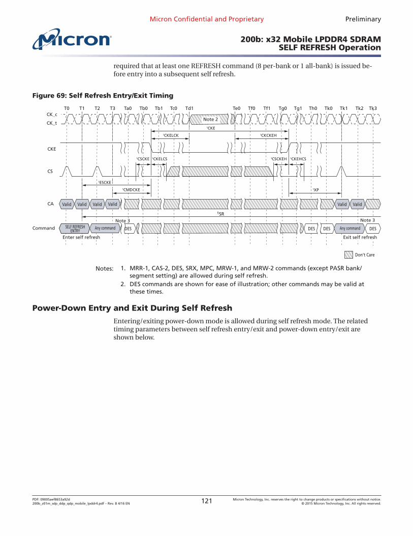
required that at least one REFRESH command (8 per-bank or 1 all-bank) is issued be-fore entry into a subsequent self refresh.
Figure 69: Self Refresh Entry/Exit Timing
T0
CK_t
CK_cT1 T2 T3
CA
Command
CS
CKE
Don’t Care
Tg0Tb0 Tk2Tb1 Tc0 Td1 Tf1Te0Ta0 Tk0 Tk1 Tk3Tf0 Tg1 Th0
MR Write-2
Valid Valid
SELF REFRESHENTRY DES DES DES
tSR
Valid
Any command DES
tCKELCK tCKCKEH
tCKE
tCSCKE
t
tCMDCKE
tCKELCS tCSCKEH tCKEHCS
Note 3
Note 2
tXP
ValidValid Valid
ESCKE
Enter self refresh Exit self refresh
Any command
Note 3
Notes: 1. MRR-1, CAS-2, DES, SRX, MPC, MRW-1, and MRW-2 commands (except PASR bank/segment setting) are allowed during self refresh.
2. DES commands are shown for ease of illustration; other commands may be valid atthese times.
Power-Down Entry and Exit During Self Refresh
Entering/exiting power-down mode is allowed during self refresh mode. The relatedtiming parameters between self refresh entry/exit and power-down entry/exit areshown below.
Micron Confidential and Proprietary Preliminary
200b: x32 Mobile LPDDR4 SDRAMSELF REFRESH Operation
PDF: 09005aef8653a92d200b_z01m_sdp_ddp_qdp_mobile_lpddr4.pdf – Rev. B 4/16 EN 121 Micron Technology, Inc. reserves the right to change products or specifications without notice.
© 2015 Micron Technology, Inc. All rights reserved.
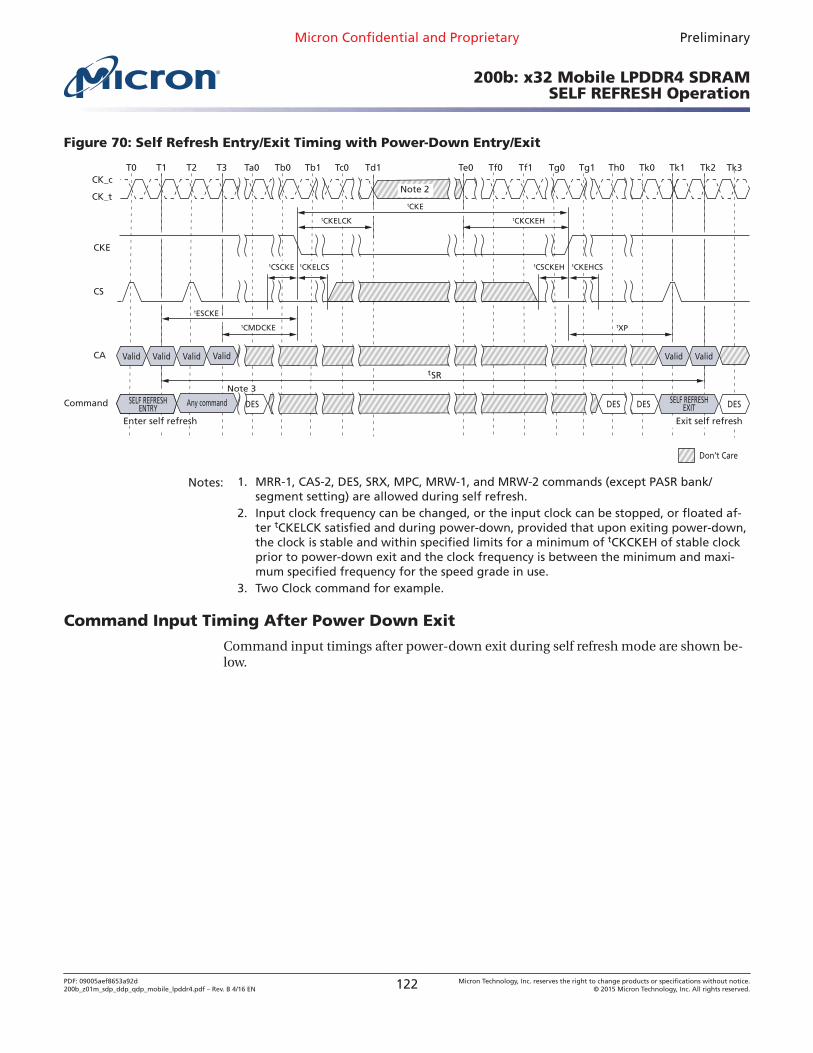
Figure 70: Self Refresh Entry/Exit Timing with Power-Down Entry/Exit
T0
CK_t
CK_cT1 T2 T3
CA
Command
CS
CKE
Don’t Care
Tg0Tb0 Tk2Tb1 Tc0 Td1 Tf1Te0Ta0 Tk0 Tk1 Tk3Tf0 Tg1 Th0
MR Write-2
Valid Valid
SELF REFRESHENTRY DES DES DES
tSR
Valid
Any command DES
tCKELCK tCKCKEH
tCKE
tCSCKE
t
tCMDCKE
tCKELCS tCSCKEH tCKEHCS
Note 3
Note 2
tXP
SELF REFRESHEXIT
ValidValid Valid
ESCKE
Enter self refresh Exit self refresh
Notes: 1. MRR-1, CAS-2, DES, SRX, MPC, MRW-1, and MRW-2 commands (except PASR bank/segment setting) are allowed during self refresh.
2. Input clock frequency can be changed, or the input clock can be stopped, or floated af-ter tCKELCK satisfied and during power-down, provided that upon exiting power-down,the clock is stable and within specified limits for a minimum of tCKCKEH of stable clockprior to power-down exit and the clock frequency is between the minimum and maxi-mum specified frequency for the speed grade in use.
3. Two Clock command for example.
Command Input Timing After Power Down Exit
Command input timings after power-down exit during self refresh mode are shown be-low.
Micron Confidential and Proprietary Preliminary
200b: x32 Mobile LPDDR4 SDRAMSELF REFRESH Operation
PDF: 09005aef8653a92d200b_z01m_sdp_ddp_qdp_mobile_lpddr4.pdf – Rev. B 4/16 EN 122 Micron Technology, Inc. reserves the right to change products or specifications without notice.
© 2015 Micron Technology, Inc. All rights reserved.
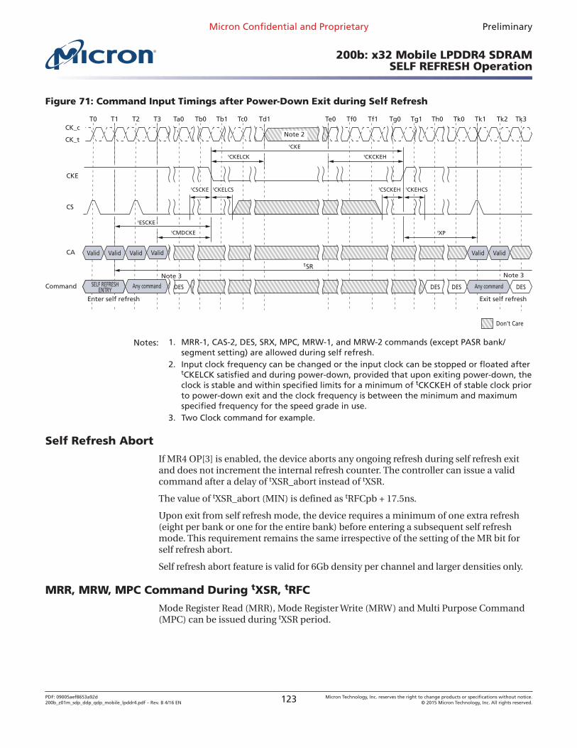
Figure 71: Command Input Timings after Power-Down Exit during Self Refresh
T0
CK_t
CK_cT1 T2 T3
CA
Command
CS
CKE
Don’t Care
Tg0Tb0 Tk2Tb1 Tc0 Td1 Tf1Te0Ta0 Tk0 Tk1 Tk3Tf0 Tg1 Th0
MR Write-2
Valid Valid
SELF REFRESHENTRY DES DES DES
tSR
Valid
Any command DES
tCKELCK tCKCKEH
tCKE
tCSCKE
t
tCMDCKE
tCKELCS tCSCKEH tCKEHCS
Note 3
Note 2
tXP
ValidValid Valid
ESCKE
Enter self refresh Exit self refresh
Any command
Note 3
Notes: 1. MRR-1, CAS-2, DES, SRX, MPC, MRW-1, and MRW-2 commands (except PASR bank/segment setting) are allowed during self refresh.
2. Input clock frequency can be changed or the input clock can be stopped or floated aftertCKELCK satisfied and during power-down, provided that upon exiting power-down, theclock is stable and within specified limits for a minimum of tCKCKEH of stable clock priorto power-down exit and the clock frequency is between the minimum and maximumspecified frequency for the speed grade in use.
3. Two Clock command for example.
Self Refresh Abort
If MR4 OP[3] is enabled, the device aborts any ongoing refresh during self refresh exitand does not increment the internal refresh counter. The controller can issue a validcommand after a delay of tXSR_abort instead of tXSR.
The value of tXSR_abort (MIN) is defined as tRFCpb + 17.5ns.
Upon exit from self refresh mode, the device requires a minimum of one extra refresh(eight per bank or one for the entire bank) before entering a subsequent self refreshmode. This requirement remains the same irrespective of the setting of the MR bit forself refresh abort.
Self refresh abort feature is valid for 6Gb density per channel and larger densities only.
MRR, MRW, MPC Command During tXSR, tRFC
Mode Register Read (MRR), Mode Register Write (MRW) and Multi Purpose Command(MPC) can be issued during tXSR period.
Micron Confidential and Proprietary Preliminary
200b: x32 Mobile LPDDR4 SDRAMSELF REFRESH Operation
PDF: 09005aef8653a92d200b_z01m_sdp_ddp_qdp_mobile_lpddr4.pdf – Rev. B 4/16 EN 123 Micron Technology, Inc. reserves the right to change products or specifications without notice.
© 2015 Micron Technology, Inc. All rights reserved.
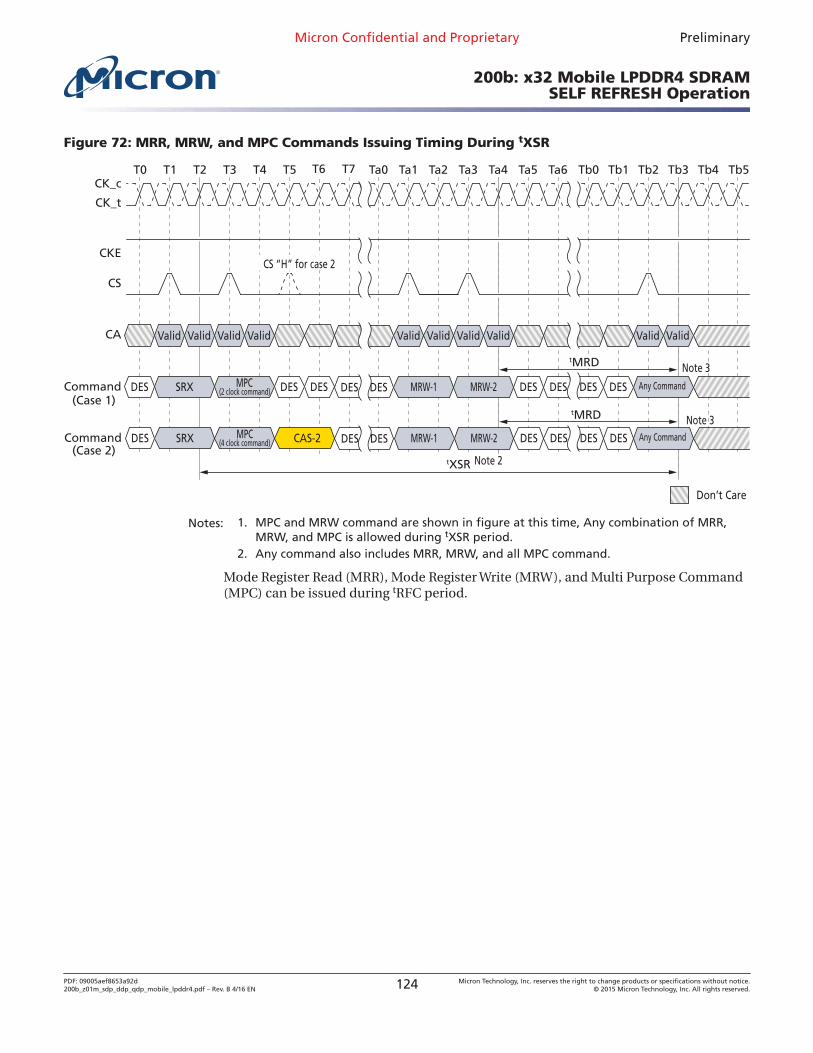
Figure 72: MRR, MRW, and MPC Commands Issuing Timing During tXSR
CK_t
CK_c
CA
CS
CKECS “H” for case 2
T0 T1 T2 T3 Ta5
Valid
T4 Tb0Ta3 Tb1 Tb4 Tb5Tb2Ta0 Ta1 Ta2 Ta4T5 T6 T7 Tb3Ta6
DES DES DES
Valid Valid Valid Valid Valid Valid Valid
DES DES DES DES
Valid Valid
MRW-1SRX MPC(2 clock command) MRW-2 Any CommandCommand
(Case 1)
(Case 2)
Don’t Care
DES DES
DES DES DES DES DESMRW-1SRX CAS-2MPC(4 clock command) MRW-2 Any CommandCommand DES DES
tMRD
tMRD
tXSR Note 2
Note 3
Note 3
Notes: 1. MPC and MRW command are shown in figure at this time, Any combination of MRR,MRW, and MPC is allowed during tXSR period.
2. Any command also includes MRR, MRW, and all MPC command.
Mode Register Read (MRR), Mode Register Write (MRW), and Multi Purpose Command(MPC) can be issued during tRFC period.
Micron Confidential and Proprietary Preliminary
200b: x32 Mobile LPDDR4 SDRAMSELF REFRESH Operation
PDF: 09005aef8653a92d200b_z01m_sdp_ddp_qdp_mobile_lpddr4.pdf – Rev. B 4/16 EN 124 Micron Technology, Inc. reserves the right to change products or specifications without notice.
© 2015 Micron Technology, Inc. All rights reserved.

Figure 73: MRR, MRW, and MPC Commands Issuing Timing During tRFC
CK_t
CK_c
CA
CS
CKECS “H” for case 2
T0 T1 T2 T3 Ta5
Valid
T4 Tb0Ta3 Tb1 Tb4 Tb5Tb2Ta0 Ta1 Ta2 Ta4T5 T6 T7 Tb3Ta6
DES DES DES
Valid Valid Valid Valid Valid Valid Valid
DES DES DES DES
Valid Valid
MRW-1REF all bank MPC(2 clock command) MRW-2 Any CommandCommand
(Case 1)
(Case 2)
Don’t Care
DES DES
DES DES DES DES DESMRW-1CAS-2MPC(4 clock command) MRW-2 Any CommandCommand DES DES
tMRD
tMRD
tRFCab
REF all bank
Note 2
Note 3
Note 3
Notes: 1. MPC and MRW command are shown in figure at this time, Any combination of MRR,MRW, and MPC is allowed during tRFCab or tRFCpb period.
2. Refresh cycle time depends on REFRESH command. In case of REF PER BANK commandissued, refresh cycle time will be tRFCpb.
3. Any command also includes MRR, MRW, and all MPC command.
Micron Confidential and Proprietary Preliminary
200b: x32 Mobile LPDDR4 SDRAMSELF REFRESH Operation
PDF: 09005aef8653a92d200b_z01m_sdp_ddp_qdp_mobile_lpddr4.pdf – Rev. B 4/16 EN 125 Micron Technology, Inc. reserves the right to change products or specifications without notice.
© 2015 Micron Technology, Inc. All rights reserved.
Power-Down Mode
Power-Down Entry and Exit
Power-down is asynchronously entered when CKE is driven LOW. CKE must not go LOWwhile the following operations are in progress:
• Mode register read• Mode register write• Read• Write• VREF(CA) range and value setting via MRW• VREF(DQ) range and value setting via MRW• Command bus training mode entering/exiting via MRW• VRCG HIGH current mode entering/exiting via MRW
CKE can go LOW while any other operations such as row activation, precharge, autoprecharge, or refresh are in progress. The power-down IDD specification will not be ap-plied until such operations are complete. Power-down entry and exit are shown below.
Entering power-down deactivates the input and output buffers, excluding CKE and RE-SET_n. To ensure that there is enough time to account for internal delay on the CKE sig-nal path, CS input is required stable LOW level and CA input level is "Don’t care" afterCKE is driven LOW, this timing period is defined as tCKELCS. Clock input is required af-ter CKE is driven LOW, this timing period is defined as tCKELCK. CKE LOW will result indeactivation of all input receivers except RESET_n after tCKELCK has expired. In power-down mode, CKE must be held LOW; all other input signals except RESET_n are "Don'tCare". CKE LOW must be maintained until tCKE(MIN) is satisfied.
VDDQ can be turned off during power-down. Prior to exiting power-down, VDDQ must bewithin its minimum/maximum operating range. No refresh operations are performedin power-down mode except self refresh power-down. The maximum duration in non-self-refresh power-down mode is only limited by the refresh requirements outlined inthe refresh command section.
The power-down state is asynchronously exited when CKE is driven HIGH. CKE HIGHmust be maintained until tCKE(MIN) is satisfied. A valid, executable command can beapplied with power-down exit latency tXP after CKE goes HIGH. Power-down exit laten-cy is defined in the AC timing parameter table.
Clock frequency change or clock stop is inhibited during tCMDCKE, tCKELCK,tCKCKEH, tXP, tMRWCKEL, and tZQCKE periods.
If power-down occurs when all banks are idle, this mode is referred to as idle power-down. if power-down occurs when there is a row active in any bank, this mode is refer-red to as active power-down. And If power-down occurs when self refresh is in progress,this mode is referred to as self refresh power-down in which the internal refresh is con-tinuing in the same way as self refresh mode.
When CA, CK and/or CS ODT is enabled via MR11 OP[6:4] and also via MR22 or CA-ODT pad setting, the rank providing ODT will continue to terminate the command busin all DRAM states including power-down.
The LPDDR4 DRAM cannot be placed in power-down state during start DQS intervaloscillator operation.
Micron Confidential and Proprietary Preliminary
200b: x32 Mobile LPDDR4 SDRAMPower-Down Mode
PDF: 09005aef8653a92d200b_z01m_sdp_ddp_qdp_mobile_lpddr4.pdf – Rev. B 4/16 EN 126 Micron Technology, Inc. reserves the right to change products or specifications without notice.
© 2015 Micron Technology, Inc. All rights reserved.
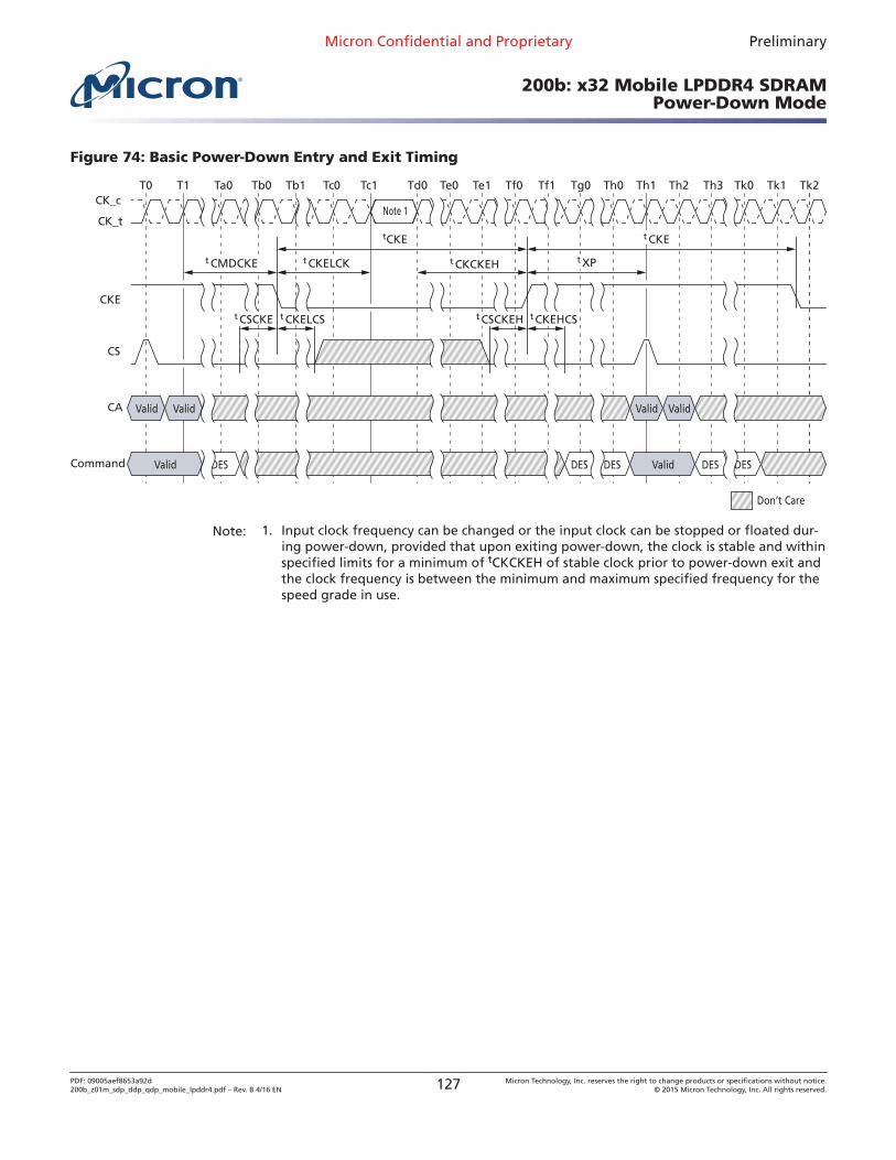
Figure 74: Basic Power-Down Entry and Exit Timing
T0
CK_t
CK_cT1 Ta0 Tb0 Th3
CA Valid
Tb1 Tc0 Th1Tc1 Te0Td0 Tf0 Tf1 Tg0 Th0
Command DES
CS
CKE
t CKCKEH
DES
Valid
Th2
Don’t Care
DES
Valid Valid
t CSCKEH
Te1
t XP
Valid DES DES
t CKEtCKE
Tk1Tk0 Tk2
Valid
t CMDCKE
t CSCKE t CKELCS
t CKELCK
Note 1
t CKEHCS
Note: 1. Input clock frequency can be changed or the input clock can be stopped or floated dur-ing power-down, provided that upon exiting power-down, the clock is stable and withinspecified limits for a minimum of tCKCKEH of stable clock prior to power-down exit andthe clock frequency is between the minimum and maximum specified frequency for thespeed grade in use.
Micron Confidential and Proprietary Preliminary
200b: x32 Mobile LPDDR4 SDRAMPower-Down Mode
PDF: 09005aef8653a92d200b_z01m_sdp_ddp_qdp_mobile_lpddr4.pdf – Rev. B 4/16 EN 127 Micron Technology, Inc. reserves the right to change products or specifications without notice.
© 2015 Micron Technology, Inc. All rights reserved.
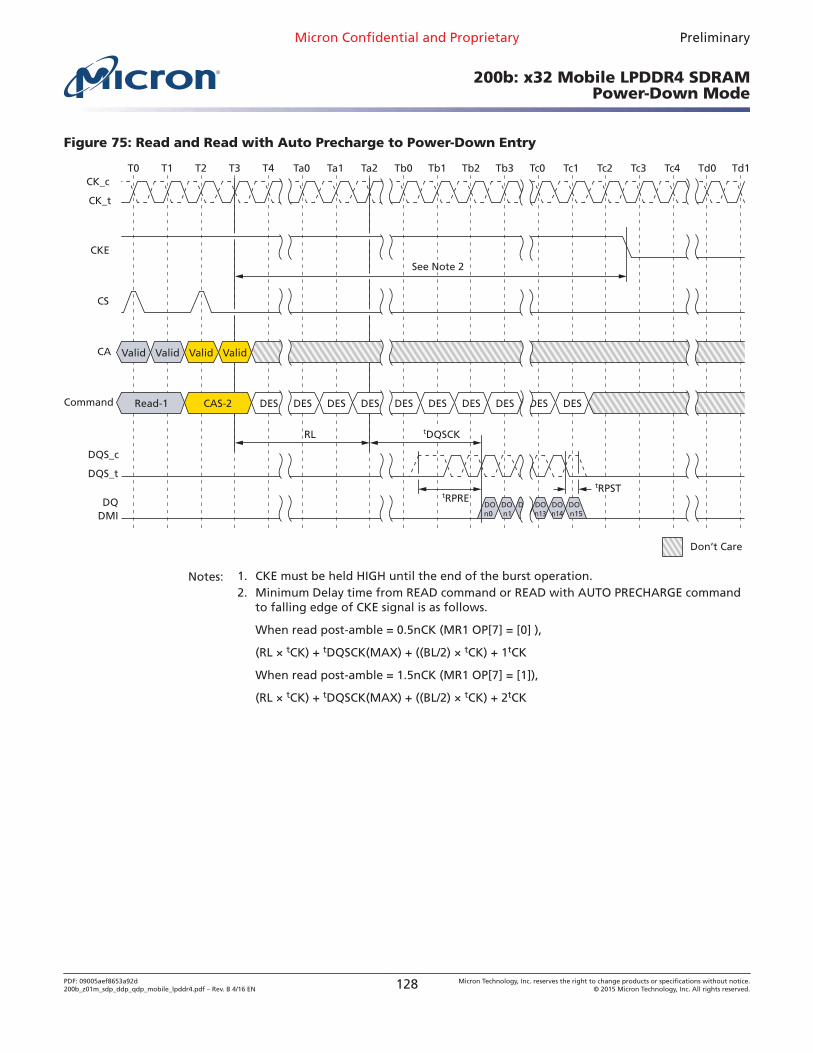
Figure 75: Read and Read with Auto Precharge to Power-Down Entry
T0
CK_t
CK_cT1 T2 T3 Tc3
CA Valid
T4 Ta0 Tc1Ta1 Tb0Ta2 Tb2 Tb3 Tc0
Command Read-1
CS
CKE
Valid
Tc2
See Note 2
Tb1 Td0Tc4 Td1
Valid
CAS-2
Valid
DOn0
DOn1
DOn2
DOn13
DOn14
DOn15
RL
tRPREtRPST
tDQSCK
DQS_t
DQS_c
DQDMI
DES DES DES DES DES DES DES DES DES DES
Don’t Care
Notes: 1. CKE must be held HIGH until the end of the burst operation.2. Minimum Delay time from READ command or READ with AUTO PRECHARGE command
to falling edge of CKE signal is as follows.
When read post-amble = 0.5nCK (MR1 OP[7] = [0] ),
(RL × tCK) + tDQSCK(MAX) + ((BL/2) × tCK) + 1tCK
When read post-amble = 1.5nCK (MR1 OP[7] = [1]),
(RL × tCK) + tDQSCK(MAX) + ((BL/2) × tCK) + 2tCK
Micron Confidential and Proprietary Preliminary
200b: x32 Mobile LPDDR4 SDRAMPower-Down Mode
PDF: 09005aef8653a92d200b_z01m_sdp_ddp_qdp_mobile_lpddr4.pdf – Rev. B 4/16 EN 128 Micron Technology, Inc. reserves the right to change products or specifications without notice.
© 2015 Micron Technology, Inc. All rights reserved.
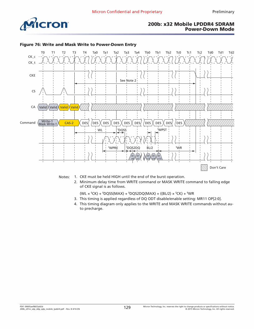
Figure 76: Write and Mask Write to Power-Down Entry
T0
CK_t
CK_cT1 T2 T3 Td0
CA Valid
T4 Ta0 Tc1Ta1 Tb0Ta2 Tb2Ta3 Ta4 Tc0
Command Write-1Mask Write-1
CS
CKE
Valid
Tc2
See Note 2
Tb1 Td2Td1
Valid
CAS-2
Valid
DIn0
DIn1
DIn2
DIn13
DIn14
DIn15
WL
DES DES DES DES DES DES DES DES DES DES
tDQSS
tWPRE tDQS2DQ BL/2 tWR
Don’t Care
tWPST
Notes: 1. CKE must be held HIGH until the end of the burst operation.2. Minimum delay time from WRITE command or MASK WRITE command to falling edge
of CKE signal is as follows.
(WL × tCK) + tDQSS(MAX) + tDQS2DQ(MAX) + ((BL/2) × tCK) + tWR3. This timing is applied regardless of DQ ODT disable/enable setting: MR11 OP[2:0].4. This timing diagram only applies to the WRITE and MASK WRITE commands without au-
to precharge.
Micron Confidential and Proprietary Preliminary
200b: x32 Mobile LPDDR4 SDRAMPower-Down Mode
PDF: 09005aef8653a92d200b_z01m_sdp_ddp_qdp_mobile_lpddr4.pdf – Rev. B 4/16 EN 129 Micron Technology, Inc. reserves the right to change products or specifications without notice.
© 2015 Micron Technology, Inc. All rights reserved.
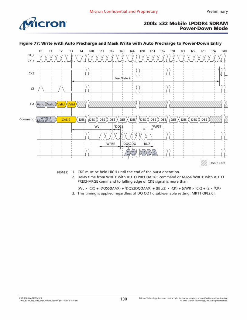
Figure 77: Write with Auto Precharge and Mask Write with Auto Precharge to Power-Down Entry
CK_t
CK_c
CA Valid
Command Write-1Mask Write-1
CS
CKE
Valid
See Note 2
Valid
CAS-2
Valid
DIn0
DIn1
DIn2
DIn13
DIn14
DIn15
WL
DES DES DES DES DES DES DES DES DES
tDQSS
tWPRE tDQS2DQ BL/2
DES DES DES DES
Don’t Care
T0 T1 T2 T3 Tc3T4 Ta0 Tc1Ta1 Tb0Ta2 Tb2Ta3 Ta4 Tc0 Tc2Tb1 Td0Tc4
tWPST
Notes: 1. CKE must be held HIGH until the end of the burst operation.2. Delay time from WRITE with AUTO PRECHARGE command or MASK WRITE with AUTO
PRECHARGE command to falling edge of CKE signal is more than
(WL × tCK) + tDQSS(MAX) + tDQS2DQ(MAX) + ((BL/2) × tCK) + (nWR × tCK) + (2 × tCK)3. This timing is applied regardless of DQ ODT disable/enable setting: MR11 OP[2:0].
Micron Confidential and Proprietary Preliminary
200b: x32 Mobile LPDDR4 SDRAMPower-Down Mode
PDF: 09005aef8653a92d200b_z01m_sdp_ddp_qdp_mobile_lpddr4.pdf – Rev. B 4/16 EN 130 Micron Technology, Inc. reserves the right to change products or specifications without notice.
© 2015 Micron Technology, Inc. All rights reserved.
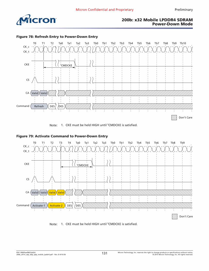
Figure 78: Refresh Entry to Power-Down Entry
T0
CK_t
CK_cT1 T2 Ta0 Tb8Ta1 Tb6Tb1Tb0 Tb3 Tb4 Tb5 Tb7Tb2 Tb10Tb9Ta2 Ta3
CA Valid
Command Refresh
CS
CKE
Valid
DES
tCMDCKE
DES
Don’t Care
Note: 1. CKE must be held HIGH until tCMDCKE is satisfied.
Figure 79: Activate Command to Power-Down Entry
T0
CK_t
CK_cT1 T2 T3 Tb6
CA Valid
T4 Tb0 Tb4Tb1 Tb9Tb2Ta1 Ta2 Ta3
Command Activate-1
CS
CKE
Valid
Tb5Ta0 Tb8Tb7
DES
tCMDCKE
Valid Valid
Activate-2 DES
Don’t Care
Note: 1. CKE must be held HIGH until tCMDCKE is satisfied.
Micron Confidential and Proprietary Preliminary
200b: x32 Mobile LPDDR4 SDRAMPower-Down Mode
PDF: 09005aef8653a92d200b_z01m_sdp_ddp_qdp_mobile_lpddr4.pdf – Rev. B 4/16 EN 131 Micron Technology, Inc. reserves the right to change products or specifications without notice.
© 2015 Micron Technology, Inc. All rights reserved.
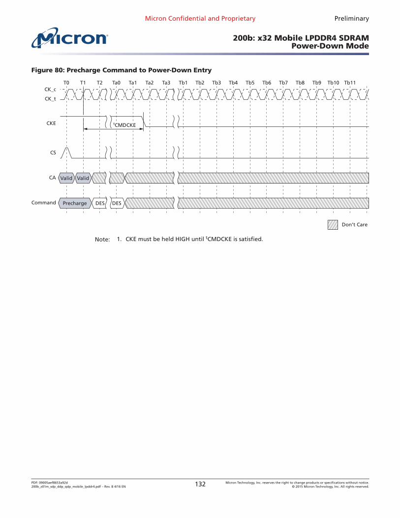
Figure 80: Precharge Command to Power-Down Entry
T0
CK_t
CK_cT1 T2 Tb1 Tb8
CA Valid
Tb2 Tb6Ta1Ta0 Ta3 Tb4 Tb5
Command Precharge
CS
CKE
Valid
Tb7Ta2 Tb10Tb9
DES
tCMDCKE
Tb11Tb3
DES
Don’t Care
Note: 1. CKE must be held HIGH until tCMDCKE is satisfied.
Micron Confidential and Proprietary Preliminary
200b: x32 Mobile LPDDR4 SDRAMPower-Down Mode
PDF: 09005aef8653a92d200b_z01m_sdp_ddp_qdp_mobile_lpddr4.pdf – Rev. B 4/16 EN 132 Micron Technology, Inc. reserves the right to change products or specifications without notice.
© 2015 Micron Technology, Inc. All rights reserved.
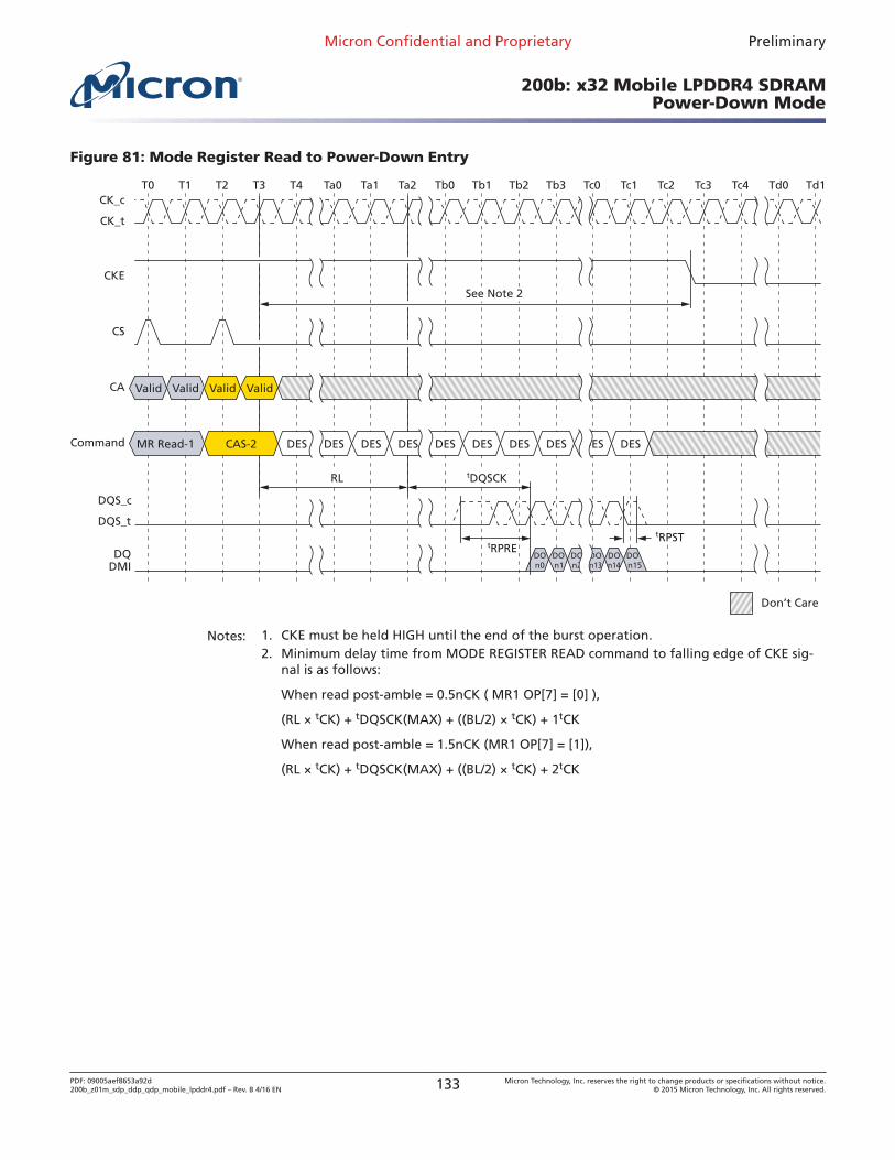
Figure 81: Mode Register Read to Power-Down Entry
T0
CK_t
CK_cT1 T2 T3 Tc3
CA Valid
T4 Ta0 Tc1Ta1 Tb0Ta2 Tb2 Tb3 Tc0
Command MR Read-1
CS
CKE
Valid
Tc2
See Note 2
Tb1 Td0Tc4 Td1
Valid
CAS-2
Valid
DOn0
DOn1
DOn2
DOn13
DOn14
DOn15
RL
tRPREtRPST
tDQSCK
DQS_t
DQS_c
DQDMI
DES DES DES DES DES DES DES DES DES DES
Don’t Care
Notes: 1. CKE must be held HIGH until the end of the burst operation.2. Minimum delay time from MODE REGISTER READ command to falling edge of CKE sig-
nal is as follows:
When read post-amble = 0.5nCK ( MR1 OP[7] = [0] ),
(RL × tCK) + tDQSCK(MAX) + ((BL/2) × tCK) + 1tCK
When read post-amble = 1.5nCK (MR1 OP[7] = [1]),
(RL × tCK) + tDQSCK(MAX) + ((BL/2) × tCK) + 2tCK
Micron Confidential and Proprietary Preliminary
200b: x32 Mobile LPDDR4 SDRAMPower-Down Mode
PDF: 09005aef8653a92d200b_z01m_sdp_ddp_qdp_mobile_lpddr4.pdf – Rev. B 4/16 EN 133 Micron Technology, Inc. reserves the right to change products or specifications without notice.
© 2015 Micron Technology, Inc. All rights reserved.
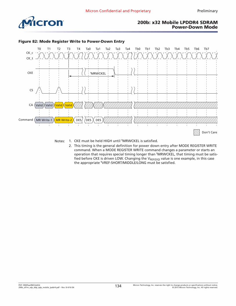
Figure 82: Mode Register Write to Power-Down Entry
T0
CK_t
CK_cT1 T2 T3 Tb1
CA Valid
T4 Tb3Ta4 Tb4 Tb7Tb5Ta1 Ta2 Ta3
Command MR Write-1
CS
CKE
Valid
Tb0Ta0 Tb6Tb2
DES
tMRWCKEL
Valid Valid
MR Write-2 DES DES
Don’t Care
Notes: 1. CKE must be held HIGH until tMRWCKEL is satisfied.2. This timing is the general definition for power down entry after MODE REGISTER WRITE
command. When a MODE REGISTER WRITE command changes a parameter or starts anoperation that requires special timing longer than tMRWCKEL, that timing must be satis-fied before CKE is driven LOW. Changing the VREF(DQ) value is one example, in this casethe appropriate tVREF-SHORT/MIDDLE/LONG must be satisfied.
Micron Confidential and Proprietary Preliminary
200b: x32 Mobile LPDDR4 SDRAMPower-Down Mode
PDF: 09005aef8653a92d200b_z01m_sdp_ddp_qdp_mobile_lpddr4.pdf – Rev. B 4/16 EN 134 Micron Technology, Inc. reserves the right to change products or specifications without notice.
© 2015 Micron Technology, Inc. All rights reserved.
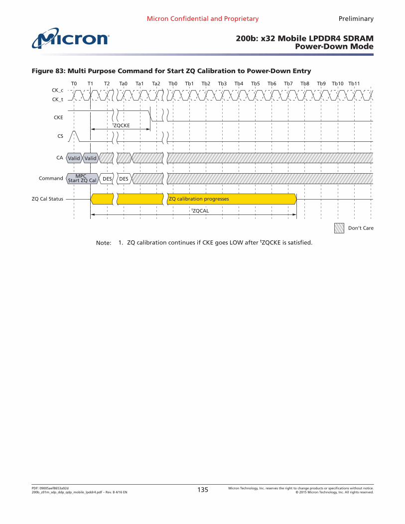
Figure 83: Multi Purpose Command for Start ZQ Calibration to Power-Down Entry
T0
CK_t
CK_cT1 T2 Tb8
CA Valid
Tb6Ta1Ta0 Tb3 Tb4 Tb5
Command MPC Start ZQ Cal
CS
CKE
Valid
Tb7Ta2 Tb10Tb9
DES
tZQCKE
Tb11
ZQ Cal Status ZQ calibration progresses
DES
Tb1Tb0 Tb2
Don’t Care
tZQCAL
Note: 1. ZQ calibration continues if CKE goes LOW after tZQCKE is satisfied.
Micron Confidential and Proprietary Preliminary
200b: x32 Mobile LPDDR4 SDRAMPower-Down Mode
PDF: 09005aef8653a92d200b_z01m_sdp_ddp_qdp_mobile_lpddr4.pdf – Rev. B 4/16 EN 135 Micron Technology, Inc. reserves the right to change products or specifications without notice.
© 2015 Micron Technology, Inc. All rights reserved.
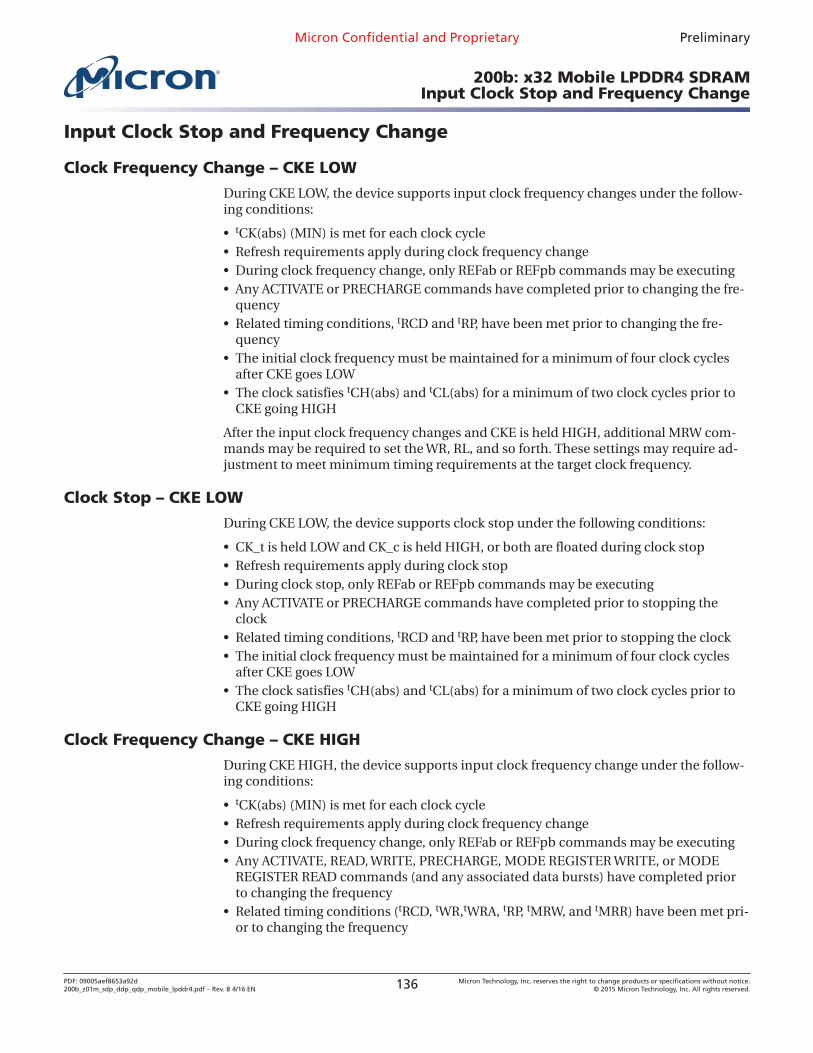
Input Clock Stop and Frequency Change
Clock Frequency Change – CKE LOW
During CKE LOW, the device supports input clock frequency changes under the follow-ing conditions:
• tCK(abs) (MIN) is met for each clock cycle• Refresh requirements apply during clock frequency change• During clock frequency change, only REFab or REFpb commands may be executing• Any ACTIVATE or PRECHARGE commands have completed prior to changing the fre-
quency• Related timing conditions, tRCD and tRP, have been met prior to changing the fre-
quency• The initial clock frequency must be maintained for a minimum of four clock cycles
after CKE goes LOW• The clock satisfies tCH(abs) and tCL(abs) for a minimum of two clock cycles prior to
CKE going HIGH
After the input clock frequency changes and CKE is held HIGH, additional MRW com-mands may be required to set the WR, RL, and so forth. These settings may require ad-justment to meet minimum timing requirements at the target clock frequency.
Clock Stop – CKE LOW
During CKE LOW, the device supports clock stop under the following conditions:
• CK_t is held LOW and CK_c is held HIGH, or both are floated during clock stop• Refresh requirements apply during clock stop• During clock stop, only REFab or REFpb commands may be executing• Any ACTIVATE or PRECHARGE commands have completed prior to stopping the
clock• Related timing conditions, tRCD and tRP, have been met prior to stopping the clock• The initial clock frequency must be maintained for a minimum of four clock cycles
after CKE goes LOW• The clock satisfies tCH(abs) and tCL(abs) for a minimum of two clock cycles prior to
CKE going HIGH
Clock Frequency Change – CKE HIGH
During CKE HIGH, the device supports input clock frequency change under the follow-ing conditions:
• tCK(abs) (MIN) is met for each clock cycle• Refresh requirements apply during clock frequency change• During clock frequency change, only REFab or REFpb commands may be executing• Any ACTIVATE, READ, WRITE, PRECHARGE, MODE REGISTER WRITE, or MODE
REGISTER READ commands (and any associated data bursts) have completed priorto changing the frequency
• Related timing conditions (tRCD, tWR,tWRA, tRP, tMRW, and tMRR) have been met pri-or to changing the frequency
Micron Confidential and Proprietary Preliminary
200b: x32 Mobile LPDDR4 SDRAMInput Clock Stop and Frequency Change
PDF: 09005aef8653a92d200b_z01m_sdp_ddp_qdp_mobile_lpddr4.pdf – Rev. B 4/16 EN 136 Micron Technology, Inc. reserves the right to change products or specifications without notice.
© 2015 Micron Technology, Inc. All rights reserved.
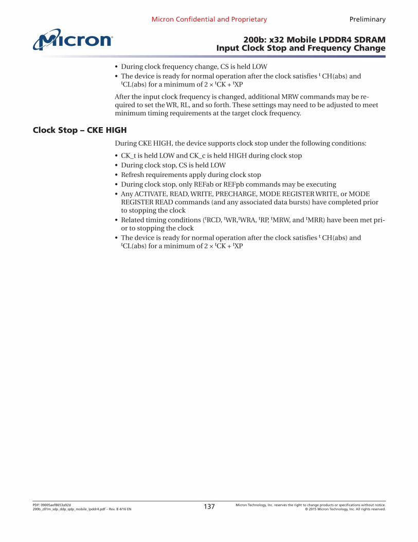
• During clock frequency change, CS is held LOW• The device is ready for normal operation after the clock satisfies t CH(abs) and
tCL(abs) for a minimum of 2 × tCK + tXP
After the input clock frequency is changed, additional MRW commands may be re-quired to set the WR, RL, and so forth. These settings may need to be adjusted to meetminimum timing requirements at the target clock frequency.
Clock Stop – CKE HIGH
During CKE HIGH, the device supports clock stop under the following conditions:
• CK_t is held LOW and CK_c is held HIGH during clock stop• During clock stop, CS is held LOW• Refresh requirements apply during clock stop• During clock stop, only REFab or REFpb commands may be executing• Any ACTIVATE, READ, WRITE, PRECHARGE, MODE REGISTER WRITE, or MODE
REGISTER READ commands (and any associated data bursts) have completed priorto stopping the clock
• Related timing conditions (tRCD, tWR,tWRA, tRP, tMRW, and tMRR) have been met pri-or to stopping the clock
• The device is ready for normal operation after the clock satisfies t CH(abs) andtCL(abs) for a minimum of 2 × tCK + tXP
Micron Confidential and Proprietary Preliminary
200b: x32 Mobile LPDDR4 SDRAMInput Clock Stop and Frequency Change
PDF: 09005aef8653a92d200b_z01m_sdp_ddp_qdp_mobile_lpddr4.pdf – Rev. B 4/16 EN 137 Micron Technology, Inc. reserves the right to change products or specifications without notice.
© 2015 Micron Technology, Inc. All rights reserved.
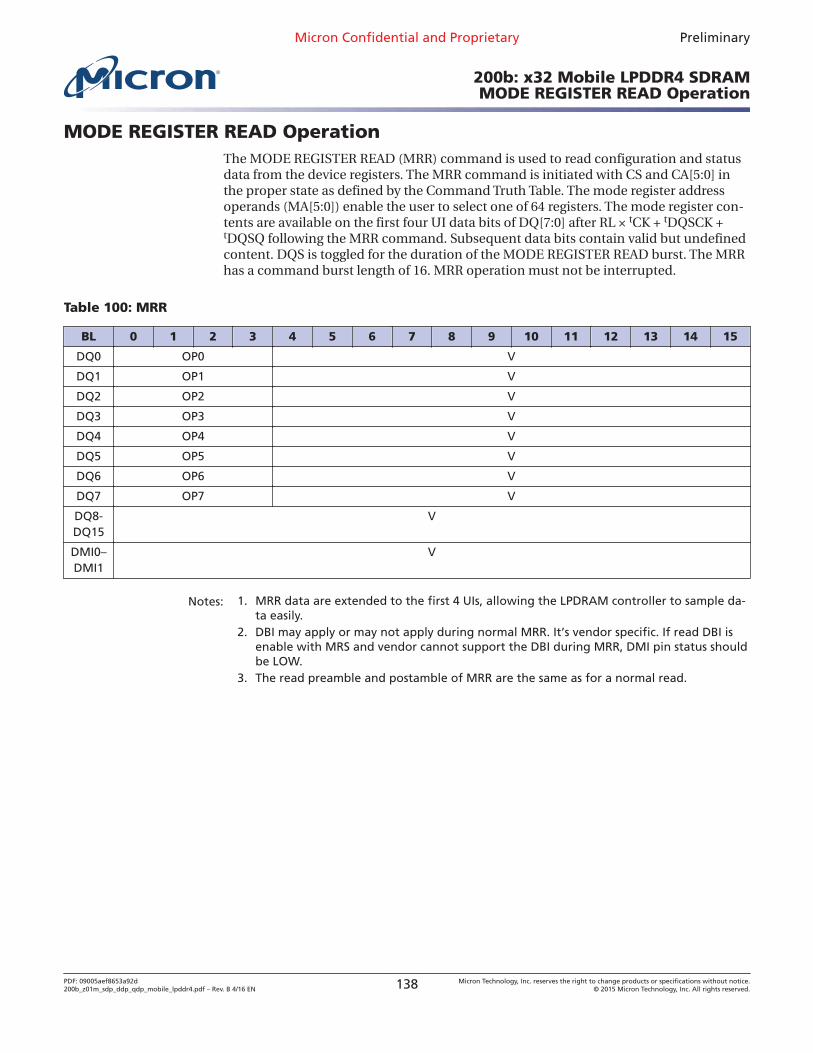
MODE REGISTER READ OperationThe MODE REGISTER READ (MRR) command is used to read configuration and statusdata from the device registers. The MRR command is initiated with CS and CA[5:0] inthe proper state as defined by the Command Truth Table. The mode register addressoperands (MA[5:0]) enable the user to select one of 64 registers. The mode register con-tents are available on the first four UI data bits of DQ[7:0] after RL × tCK + tDQSCK +tDQSQ following the MRR command. Subsequent data bits contain valid but undefinedcontent. DQS is toggled for the duration of the MODE REGISTER READ burst. The MRRhas a command burst length of 16. MRR operation must not be interrupted.
Table 100: MRR
BL 0 1 2 3 4 5 6 7 8 9 10 11 12 13 14 15
DQ0 OP0 V
DQ1 OP1 V
DQ2 OP2 V
DQ3 OP3 V
DQ4 OP4 V
DQ5 OP5 V
DQ6 OP6 V
DQ7 OP7 V
DQ8-DQ15
V
DMI0–DMI1
V
Notes: 1. MRR data are extended to the first 4 UIs, allowing the LPDRAM controller to sample da-ta easily.
2. DBI may apply or may not apply during normal MRR. It’s vendor specific. If read DBI isenable with MRS and vendor cannot support the DBI during MRR, DMI pin status shouldbe LOW.
3. The read preamble and postamble of MRR are the same as for a normal read.
Micron Confidential and Proprietary Preliminary
200b: x32 Mobile LPDDR4 SDRAMMODE REGISTER READ Operation
PDF: 09005aef8653a92d200b_z01m_sdp_ddp_qdp_mobile_lpddr4.pdf – Rev. B 4/16 EN 138 Micron Technology, Inc. reserves the right to change products or specifications without notice.
© 2015 Micron Technology, Inc. All rights reserved.
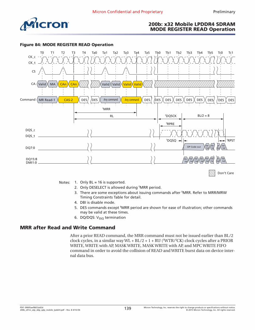
Figure 84: MODE REGISTER READ Operation
T0
CK_t
CK_cT1 T2 T3 T4 Ta0 Tc1Ta1 Tb0Ta2 Ta3 Ta4 Ta5 Tb2 Tb3 Tb4 Tb5 Tc0
CS
Tb1
CA Valid
Command MR Read-1
MA Valid Valid Valid ValidCAn
CAS-2
CAn
RL
DES DES DES DES DES DES DES DES DES DES DES
BL/2 = 8
tRPRE
tDQSCK
tRPSTtDQSQDQS_t
DQS_c
DQ7:0
DMI1:0DQ15:8
Don’t Care
Any command Any command
MRRt
Va-lidOP Code out Va-
lidVa-lid
Va-lid
Va-lid
Va-lid
Va-lid
Va-lid
Va-lid
Va-lid
Va-lid
Va-lid
Notes: 1. Only BL = 16 is supported.2. Only DESELECT is allowed during tMRR period.3. There are some exceptions about issuing commands after tMRR. Refer to MRR/MRW
Timing Constraints Table for detail.4. DBI is disable mode.5. DES commands except tMRR period are shown for ease of illustration; other commands
may be valid at these times.6. DQ/DQS: VSSQ termination
MRR after Read and Write Command
After a prior READ command, the MRR command must not be issued earlier than BL/2clock cycles, in a similar way WL + BL/2 + 1 + RU (tWTR/tCK) clock cycles after a PRIORWRITE, WRITE with AP, MASK WRITE, MASK WRITE with AP, and MPC WRITE FIFOcommand in order to avoid the collision of READ and WRITE burst data on device inter-nal data bus.
Micron Confidential and Proprietary Preliminary
200b: x32 Mobile LPDDR4 SDRAMMODE REGISTER READ Operation
PDF: 09005aef8653a92d200b_z01m_sdp_ddp_qdp_mobile_lpddr4.pdf – Rev. B 4/16 EN 139 Micron Technology, Inc. reserves the right to change products or specifications without notice.
© 2015 Micron Technology, Inc. All rights reserved.
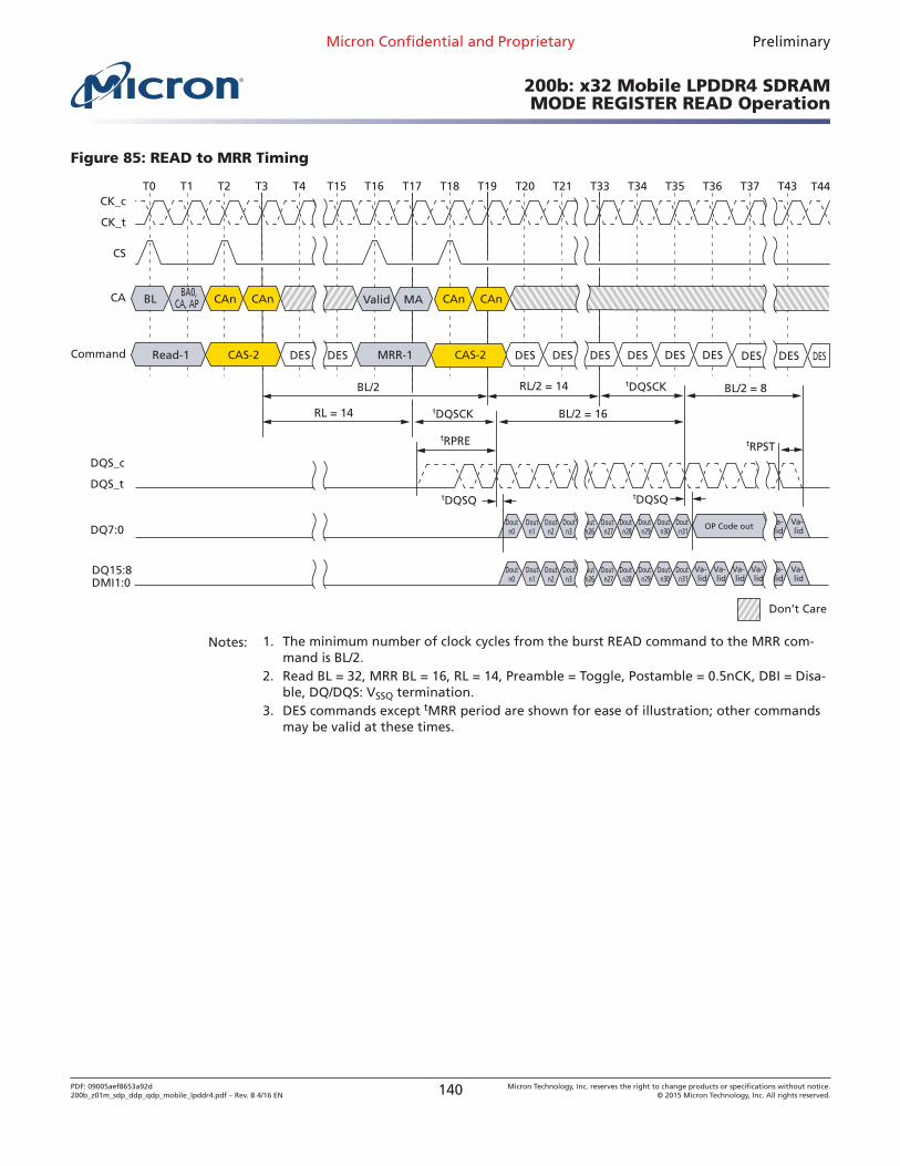
Figure 85: READ to MRR Timing
T0
CK_t
CK_cT1 T2 T3 T4 T15 T44T16 T21T17 T18 T19 T20 T34 T35 T36 T37 T43
CS
T33
CA BL
Command Read-1
BA0,CA, AP Valid MACAn
CAS-2
CAn CAn CAn
RL = 14
DES DES DES DES DES DES DES DES DES DES DES
BL/2 RL/2 = 14 BL/2 = 8
BL/2 = 16
tRPRE
tDQSCK
tDQSCK
tRPST
tDQSQDQS_t
DQS_c
DQ7:0
DMI1:0DQ15:8
Don’t Care
MRR-1 CAS-2
OP Code out Va-lid
Va-lid
Doutn0
Doutn1
Doutn2
Doutn3
Doutn26
Doutn27
Doutn28
Doutn29
Doutn30
Doutn31
tDQSQ
Va-lid
Va-lid
Va-lid
Va-lid
Va-lid
Va-lid
Doutn0
Doutn1
Doutn2
Doutn3
Doutn26
Doutn27
Doutn28
Doutn29
Doutn30
Doutn31
Notes: 1. The minimum number of clock cycles from the burst READ command to the MRR com-mand is BL/2.
2. Read BL = 32, MRR BL = 16, RL = 14, Preamble = Toggle, Postamble = 0.5nCK, DBI = Disa-ble, DQ/DQS: VSSQ termination.
3. DES commands except tMRR period are shown for ease of illustration; other commandsmay be valid at these times.
Micron Confidential and Proprietary Preliminary
200b: x32 Mobile LPDDR4 SDRAMMODE REGISTER READ Operation
PDF: 09005aef8653a92d200b_z01m_sdp_ddp_qdp_mobile_lpddr4.pdf – Rev. B 4/16 EN 140 Micron Technology, Inc. reserves the right to change products or specifications without notice.
© 2015 Micron Technology, Inc. All rights reserved.
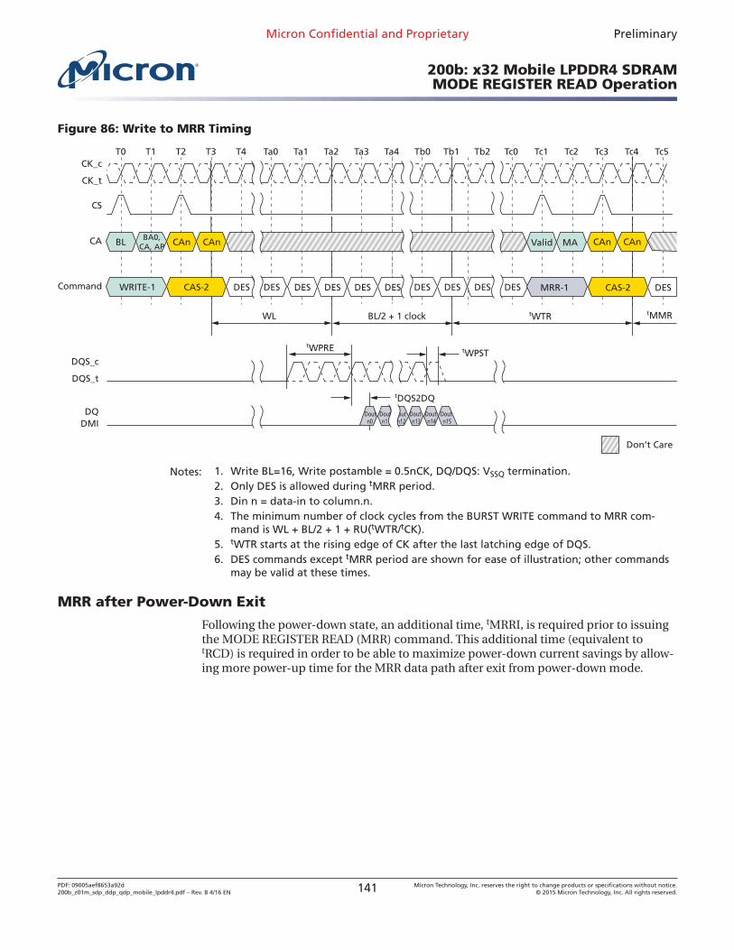
Figure 86: Write to MRR Timing
T0
CK_t
CK_cT1 T2 T3 T4 Ta0 Ta1 Tb2Ta2 Ta3 Ta4 Tb0 Tb1 Tc1 Tc2 Tc3 Tc4 Tc5
CS
Tc0
CA BL
Command WRITE-1
BA0,CA, AP Valid MACAn
CAS-2
CAn CAn CAn
BL/2 + 1 clock
DES DES DES DES DES DESDES DES DES DES DES
tWPRE tWPST
tWTR tMMR
DQS_t
DQS_c
DMIDQ
Don’t Care
WL
tDQS2DQ
MRR-1 CAS-2
Doutn0
Doutn1
Doutn12
Doutn13
Doutn14
Doutn15
Notes: 1. Write BL=16, Write postamble = 0.5nCK, DQ/DQS: VSSQ termination.2. Only DES is allowed during tMRR period.3. Din n = data-in to column.n.4. The minimum number of clock cycles from the BURST WRITE command to MRR com-
mand is WL + BL/2 + 1 + RU(tWTR/tCK).5. tWTR starts at the rising edge of CK after the last latching edge of DQS.6. DES commands except tMRR period are shown for ease of illustration; other commands
may be valid at these times.
MRR after Power-Down Exit
Following the power-down state, an additional time, tMRRI, is required prior to issuingthe MODE REGISTER READ (MRR) command. This additional time (equivalent totRCD) is required in order to be able to maximize power-down current savings by allow-ing more power-up time for the MRR data path after exit from power-down mode.
Micron Confidential and Proprietary Preliminary
200b: x32 Mobile LPDDR4 SDRAMMODE REGISTER READ Operation
PDF: 09005aef8653a92d200b_z01m_sdp_ddp_qdp_mobile_lpddr4.pdf – Rev. B 4/16 EN 141 Micron Technology, Inc. reserves the right to change products or specifications without notice.
© 2015 Micron Technology, Inc. All rights reserved.
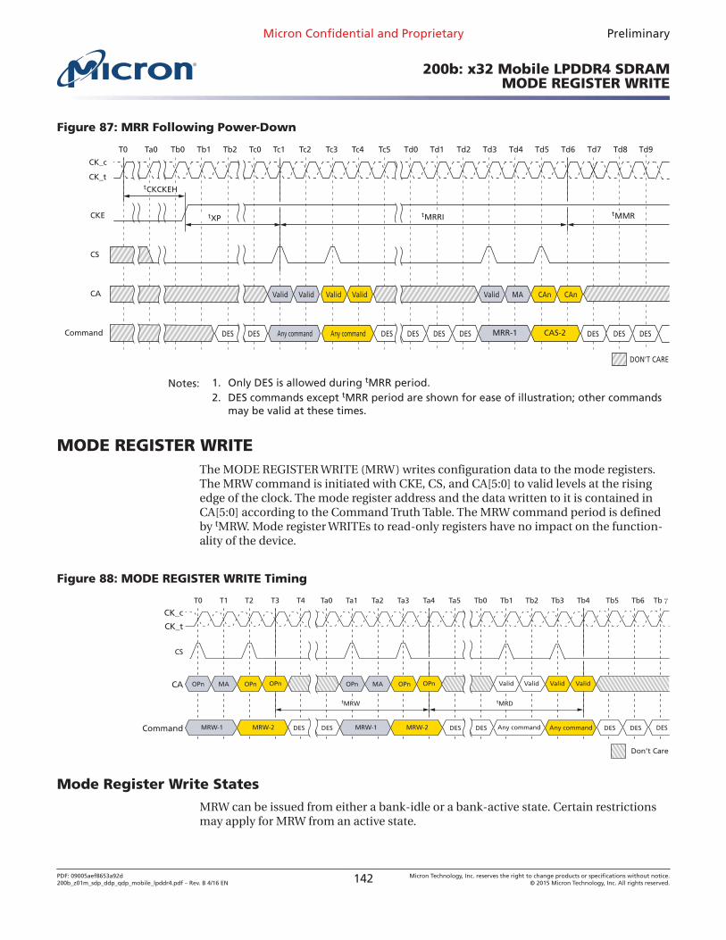
Figure 87: MRR Following Power-Down
T0
CK_t
CK_c
Ta0 Tb0 Tb1
CA
Tb2 Tc1
Command
CS
CKE
Td1
DON'T CARE
Tc0 Td7Td2Tc5 Td3 Td6Td4Tc2 Tc3 Tc4 Td0 Td5 Td8 Td9
DES
Valid Valid
DES DES DES
Valid MA
DES DES DES DES
CAn CAn
MRR-1 CAS-2DES Any command
Valid Valid
Any command
tCKCKEH
tMMRtMRRItXP
Notes: 1. Only DES is allowed during tMRR period.2. DES commands except tMRR period are shown for ease of illustration; other commands
may be valid at these times.
MODE REGISTER WRITEThe MODE REGISTER WRITE (MRW) writes configuration data to the mode registers.The MRW command is initiated with CKE, CS, and CA[5:0] to valid levels at the risingedge of the clock. The mode register address and the data written to it is contained inCA[5:0] according to the Command Truth Table. The MRW command period is definedby tMRW. Mode register WRITEs to read-only registers have no impact on the function-ality of the device.
Figure 88: MODE REGISTER WRITE Timing
T0 T1 T2 T3 T4 Ta0 Ta2Ta1
CK_c
CK_t
Ta4 Ta5Ta3 Tb0 Tb1 Tb3 Tb4Tb2 Tb6 Tb7Tb5
CA
Command
tMRW tMRD
MAOPn OPn OPn MAOPn OPn OPn
MRW-2MRW-1 MRW-1 MRW-2 Any command Any command
Valid Valid Valid Valid
CS
Don’t Care
DES DES DES DES DES DES DES
Mode Register Write States
MRW can be issued from either a bank-idle or a bank-active state. Certain restrictionsmay apply for MRW from an active state.
Micron Confidential and Proprietary Preliminary
200b: x32 Mobile LPDDR4 SDRAMMODE REGISTER WRITE
PDF: 09005aef8653a92d200b_z01m_sdp_ddp_qdp_mobile_lpddr4.pdf – Rev. B 4/16 EN 142 Micron Technology, Inc. reserves the right to change products or specifications without notice.
© 2015 Micron Technology, Inc. All rights reserved.
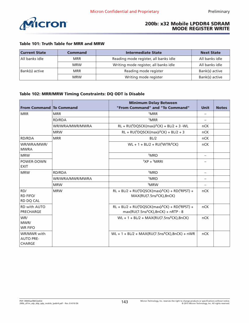
Table 101: Truth Table for MRR and MRW
Current State Command Intermediate State Next State
All banks idle MRR Reading mode register, all banks idle All banks idle
MRW Writing mode register, all banks idle All banks idle
Bank(s) active MRR Reading mode register Bank(s) active
MRW Writing mode register Bank(s) active
Table 102: MRR/MRW Timing Constraints: DQ ODT is Disable
From Command To CommandMinimum Delay Between
"From Command" and "To Command" Unit Notes
MRR MRR tMRR –
RD/RDA tMRR –
WR/WRA/MWR/MWRA RL + RU(tDQSCK(max)/tCK) + BL/2 + 3 -WL nCK
MRW RL + RU(tDQSCK(max)/tCK) + BL/2 + 3 nCK
RD/RDA MRR BL/2 nCK
WR/WRA/MWR/MWRA
WL + 1 + BL/2 + RU(tWTR/tCK) nCK
MRW tMRD –
POWER-DOWNEXIT
tXP + tMRRI –
MRW RD/RDA tMRD –
WR/WRA/MWR/MWRA tMRD –
MRW tMRW –
RD/RD FIFO/RD DQ CAL
MRW RL + BL/2 + RU(tDQSCK(max)/tCK) + RD(tRPST) +MAX(RU(7.5ns/tCK),8nCK)
nCK
RD with AUTOPRECHARGE
RL + BL/2 + RU(tDQSCK(max)/tCK) + RD(tRPST) +max(RU(7.5ns/tCK),8nCK) + nRTP - 8
nCK
WR/MWR/WR FIFO
WL + 1 + BL/2 + MAX(RU(7.5ns/tCK),8nCK) nCK
WR/MWR withAUTO PRE-CHARGE
WL + 1 + BL/2 + MAX(RU(7.5ns/tCK),8nCK) + nWR nCK
Micron Confidential and Proprietary Preliminary
200b: x32 Mobile LPDDR4 SDRAMMODE REGISTER WRITE
PDF: 09005aef8653a92d200b_z01m_sdp_ddp_qdp_mobile_lpddr4.pdf – Rev. B 4/16 EN 143 Micron Technology, Inc. reserves the right to change products or specifications without notice.
© 2015 Micron Technology, Inc. All rights reserved.
Table 103: MRR/MRW Timing Constraints: DQ ODT is Enable
From Command To CommandMinimum Delay Between
"From Command" and "To Command" Unit Notes
MRR MRR tMRR –
RD/RDA tMRR –
WR/WRA/MWR/MWRA RL + RU(tDQSCK(max)/tCK) + BL/2 + 3 - ODTLon -RD(tODTon(min)/tCK)
nCK
MRW RL + RU(tDQSCK(max)/tCK) + BL/2 + 3 nCK
RD/RDA MRR BL/2 nCK
WR/WRA/MWR/MWRA
WL + 1 + BL/2 + RU(tWTR/tCK) nCK
MRW tMRD –
POWER-DOWNEXIT
tXP + tMRRI –
MRW RD/RDA tMRD –
WR/WRA/MWR/MWRA tMRD –
MRW tMRW –
RD/RD FIFO/RD DQ CAL
MRW RL + BL/2 + RU(tDQSCK(max)/tCK) + RD(tRPST) +MAX(RU(7.5ns/tCK),8nCK)
nCK
RD with AUTOPRECHARGE
RL + BL/2 + RU(tDQSCK(max)/tCK) + RD(tRPST) +max(RU(7.5ns/tCK),8nCK) + nRTP - 8
nCK
WR/MWR/WR FIFO
WL + 1 + BL/2 + MAX(RU(7.5ns/tCK),8nCK) nCK
WR/MWR withAUTO PRE-CHARGE
WL + 1 + BL/2 + MAX(RU(7.5ns/tCK),8nCK) + nWR nCK
VREF Current Generator (VRCG)LPDDR4 SDRAM VREF current generators (VRCG) incorporate a high current mode toreduce the settling time of the internal VREF(DQ) and VREF(CA) levels during training andwhen changing frequency set points during operation. The high current mode is ena-bled by setting MR13[OP3] = 1. Only deselect commands may be issued untiltVRCG_ENABLE is satisfied. tVRCG_ENABLE timing is shown below.
Micron Confidential and Proprietary Preliminary
200b: x32 Mobile LPDDR4 SDRAMVREF Current Generator (VRCG)
PDF: 09005aef8653a92d200b_z01m_sdp_ddp_qdp_mobile_lpddr4.pdf – Rev. B 4/16 EN 144 Micron Technology, Inc. reserves the right to change products or specifications without notice.
© 2015 Micron Technology, Inc. All rights reserved.
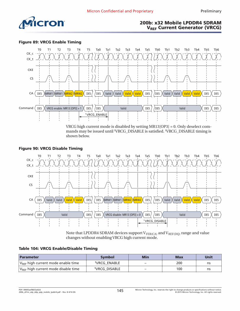
Figure 89: VRCG Enable Timing
T0
CK_t
CK_cT1 T2 T3 T4
CA MRW1 MRW2MRW1 MRW2
T5 Ta0 Ta1 Ta2 Ta3 Ta4 Ta5 Tb0 Tb1 Tb2 Tb3 Tb4 Tb5 Tb6
DES
Command DES VRCG enable: MR13 [OP3] = 1
DES
DES
DES
DES
ValidValid ValidValid DES
DESValid
t VRCG_ENABLE
DES DES DES
DES DES DES
CS
CKE
ValidValid ValidValid
Valid
VRCG high current mode is disabled by setting MR13[OP3] = 0. Only deselect com-mands may be issued until tVRCG_DISABLE is satisfied. tVRCG_DISABLE timing isshown below.
Figure 90: VRCG Disable Timing
T0
CK_t
CK_cT1 T2 T3 T4
CA
T5 Ta0 Ta1 Ta2 Ta3 Ta4 Ta5 Tb0 Tb1 Tb2 Tb3 Tb4 Tb5 Tb6
DES
Command DES
DES
DES
DES
DES
ValidValid ValidValid DES
DESValid
ValidValid ValidMRW1 MRW2MRW1 DES DES DES
DES DES DES
t VRCG_DISABLE
CS
CKE
ValidMRW2
VRCG disable: MR13 [OP3] = 0 Valid
Note that LPDDR4 SDRAM devices support VFER(CA) and VREF(DQ) range and valuechanges without enabling VRCG high current mode.
Table 104: VRCG Enable/Disable Timing
Parameter Symbol Min Max Unit
VREF high current mode enable time tVRCG_ENABLE – 200 ns
VREF high current mode disable time tVRCG_DISABLE – 100 ns
Micron Confidential and Proprietary Preliminary
200b: x32 Mobile LPDDR4 SDRAMVREF Current Generator (VRCG)
PDF: 09005aef8653a92d200b_z01m_sdp_ddp_qdp_mobile_lpddr4.pdf – Rev. B 4/16 EN 145 Micron Technology, Inc. reserves the right to change products or specifications without notice.
© 2015 Micron Technology, Inc. All rights reserved.
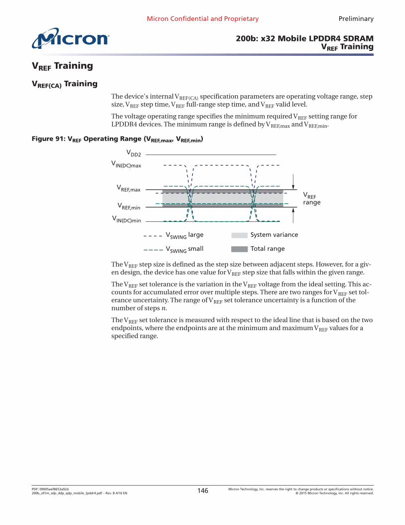
VREF Training
VREF(CA) Training
The device's internal VREF(CA) specification parameters are operating voltage range, stepsize, VREF step time, VREF full-range step time, and VREF valid level.
The voltage operating range specifies the minimum required VREF setting range forLPDDR4 devices. The minimum range is defined by VREF,max and VREF,min.
Figure 91: VREF Operating Range (VREF,max, VREF,min)
VREF,maxVREFrange
VSWING large System variance
Total rangeVSWING small
VREF,min
VIN(DC)min
VIN(DC)max
VDD2
The VREF step size is defined as the step size between adjacent steps. However, for a giv-en design, the device has one value for VREF step size that falls within the given range.
The VREF set tolerance is the variation in the VREF voltage from the ideal setting. This ac-counts for accumulated error over multiple steps. There are two ranges for VREF set tol-erance uncertainty. The range of VREF set tolerance uncertainty is a function of thenumber of steps n.
The VREF set tolerance is measured with respect to the ideal line that is based on the twoendpoints, where the endpoints are at the minimum and maximum VREF values for aspecified range.
Micron Confidential and Proprietary Preliminary
200b: x32 Mobile LPDDR4 SDRAMVREF Training
PDF: 09005aef8653a92d200b_z01m_sdp_ddp_qdp_mobile_lpddr4.pdf – Rev. B 4/16 EN 146 Micron Technology, Inc. reserves the right to change products or specifications without notice.
© 2015 Micron Technology, Inc. All rights reserved.
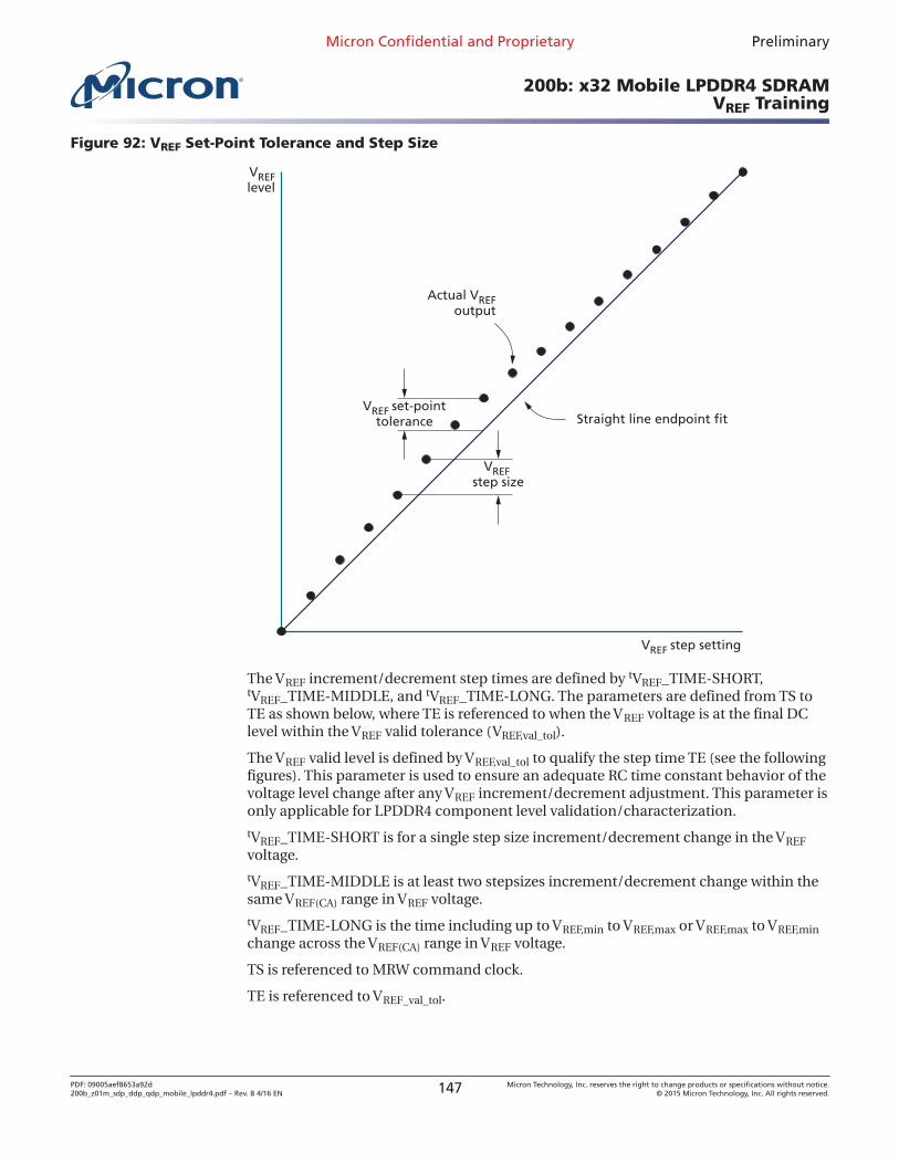
Figure 92: VREF Set-Point Tolerance and Step Size
VREFlevel
VREF step setting
Actual VREFoutput
VREF set-pointtolerance
VREF step size
Straight line endpoint fit
The VREF increment/decrement step times are defined by tVREF_TIME-SHORT,tVREF_TIME-MIDDLE, and tVREF_TIME-LONG. The parameters are defined from TS toTE as shown below, where TE is referenced to when the VREF voltage is at the final DClevel within the VREF valid tolerance (VREF,val_tol).
The VREF valid level is defined by VREF,val_tol to qualify the step time TE (see the followingfigures). This parameter is used to ensure an adequate RC time constant behavior of thevoltage level change after any VREF increment/decrement adjustment. This parameter isonly applicable for LPDDR4 component level validation/characterization.
tVREF_TIME-SHORT is for a single step size increment/decrement change in the VREFvoltage.
tVREF_TIME-MIDDLE is at least two stepsizes increment/decrement change within thesame VREF(CA) range in VREF voltage.
tVREF_TIME-LONG is the time including up to VREF,min to VREF,max or VREF,max to VREF,minchange across the VREF(CA) range in VREF voltage.
TS is referenced to MRW command clock.
TE is referenced to VREF_val_tol.
Micron Confidential and Proprietary Preliminary
200b: x32 Mobile LPDDR4 SDRAMVREF Training
PDF: 09005aef8653a92d200b_z01m_sdp_ddp_qdp_mobile_lpddr4.pdf – Rev. B 4/16 EN 147 Micron Technology, Inc. reserves the right to change products or specifications without notice.
© 2015 Micron Technology, Inc. All rights reserved.
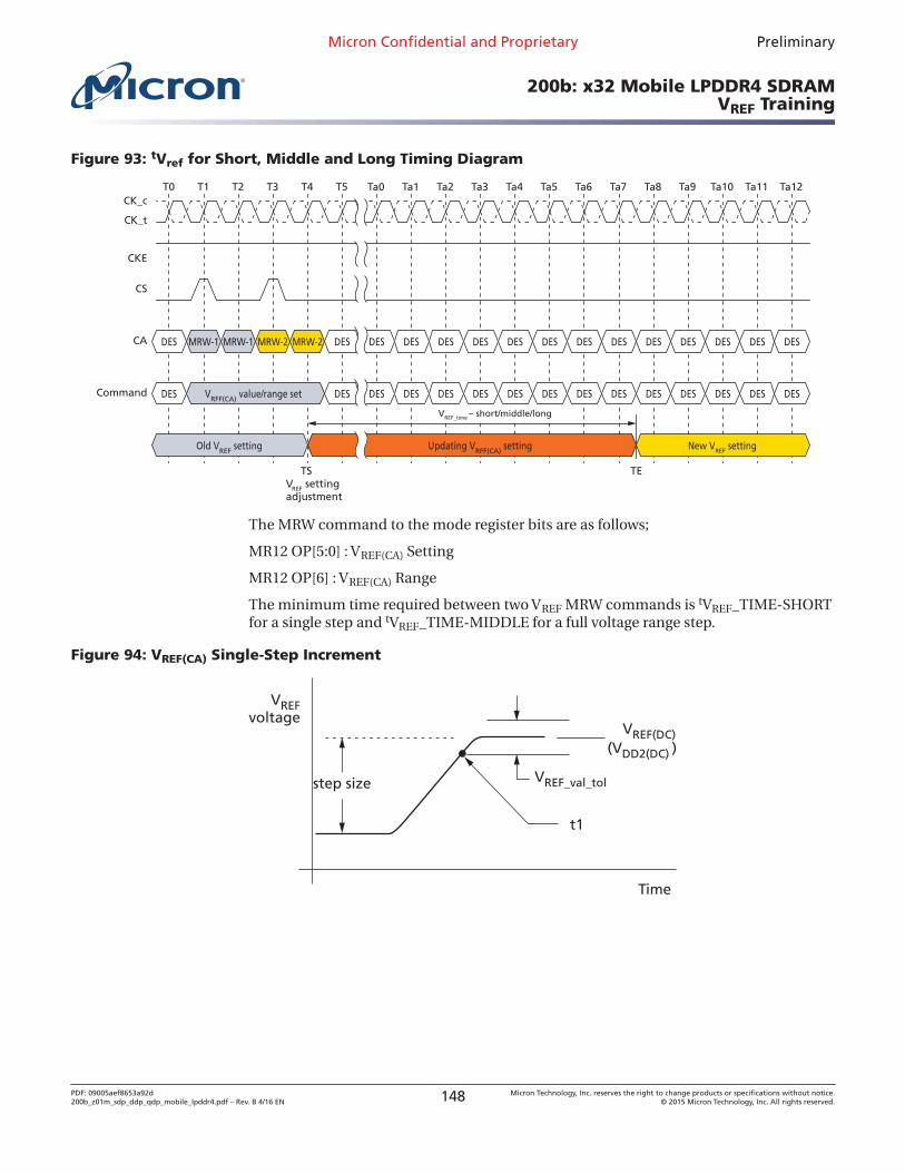
Figure 93: tVref for Short, Middle and Long Timing Diagram
T0
CK_t
CK_cT1 T2 T3 T4
CA MRW-1 MRW-2MRW-1 MRW-2
T5 Ta0 Ta1 Ta2 Ta3 Ta4 Ta5 Ta6 Ta7 Ta8 Ta9 Ta10 Ta11 Ta12
DES
Command DES VRFF(CA) value/range set
DES
DES
CS
CKE
DES DES DES DES DES DES DES DES DES DES DES DES DES
DES DES DES DES DES DES DES DES DES DES DES DES DES
Updating VRFF(CA) settingOld VREF setting New VREF setting
VREF settingadjustment
TETS
VREF_time – short/middle/long
The MRW command to the mode register bits are as follows;
MR12 OP[5:0] : VREF(CA) Setting
MR12 OP[6] : VREF(CA) Range
The minimum time required between two VREF MRW commands is tVREF_TIME-SHORTfor a single step and tVREF_TIME-MIDDLE for a full voltage range step.
Figure 94: VREF(CA) Single-Step Increment
VREFvoltage
Time
VREF(DC)(V )DD2(DC)
t1
step size VREF_val_tol
Micron Confidential and Proprietary Preliminary
200b: x32 Mobile LPDDR4 SDRAMVREF Training
PDF: 09005aef8653a92d200b_z01m_sdp_ddp_qdp_mobile_lpddr4.pdf – Rev. B 4/16 EN 148 Micron Technology, Inc. reserves the right to change products or specifications without notice.
© 2015 Micron Technology, Inc. All rights reserved.
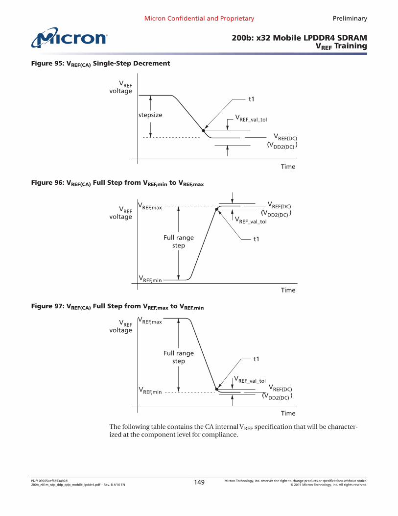
Figure 95: VREF(CA) Single-Step Decrement
VREFvoltage
Time
t1
stepsize VREF_val_tol
VREF(DC)(V )DD2(DC)
Figure 96: VREF(CA) Full Step from VREF,min to VREF,max
VREFvoltage
VREF,max
VREF,min
Time
t1Full rangestep
VREF_val_tol
VREF(DC)(V )DD2(DC)
Figure 97: VREF(CA) Full Step from VREF,max to VREF,min
VREFvoltage
VREF,max
VREF,min
Time
t1Full range
step
VREF_val_tolVREF(DC)
(V )DD2(DC)
The following table contains the CA internal VREF specification that will be character-ized at the component level for compliance.
Micron Confidential and Proprietary Preliminary
200b: x32 Mobile LPDDR4 SDRAMVREF Training
PDF: 09005aef8653a92d200b_z01m_sdp_ddp_qdp_mobile_lpddr4.pdf – Rev. B 4/16 EN 149 Micron Technology, Inc. reserves the right to change products or specifications without notice.
© 2015 Micron Technology, Inc. All rights reserved.
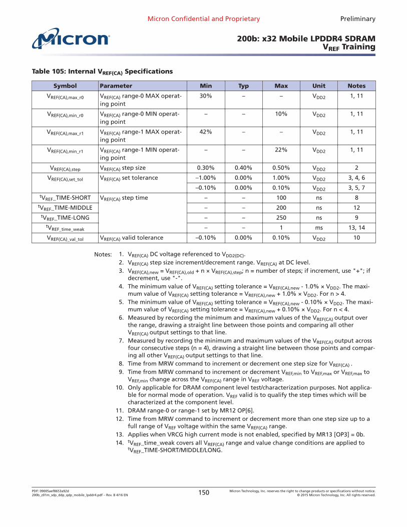
Table 105: Internal VREF(CA) Specifications
Symbol Parameter Min Typ Max Unit Notes
VREF(CA),max_r0 VREF(CA) range-0 MAX operat-ing point
30% – – VDD2 1, 11
VREF(CA),min_r0 VREF(CA) range-0 MIN operat-ing point
– – 10% VDD2 1, 11
VREF(CA),max_r1 VREF(CA) range-1 MAX operat-ing point
42% – – VDD2 1, 11
VREF(CA),min_r1 VREF(CA) range-1 MIN operat-ing point
– – 22% VDD2 1, 11
VREF(CA),step VREF(CA) step size 0.30% 0.40% 0.50% VDD2 2
VREF(CA),set_tol VREF(CA) set tolerance –1.00% 0.00% 1.00% VDD2 3, 4, 6
–0.10% 0.00% 0.10% VDD2 3, 5, 7tVREF_TIME-SHORT VREF(CA) step time – – 100 ns 8
tVREF_TIME-MIDDLE – – 200 ns 12tVREF_TIME-LONG – – 250 ns 9
tVREF_time_weak – – 1 ms 13, 14
VREF(CA)_val_tol VREF(CA) valid tolerance –0.10% 0.00% 0.10% VDD2 10
Notes: 1. VREF(CA) DC voltage referenced to VDD2(DC).2. VREF(CA) step size increment/decrement range. VREF(CA) at DC level.3. VREF(CA),new = VREF(CA),old + n × VREF(CA),step; n = number of steps; if increment, use "+"; if
decrement, use "-".4. The minimum value of VREF(CA) setting tolerance = VREF(CA),new - 1.0% × VDD2. The maxi-
mum value of VREF(CA) setting tolerance = VREF(CA),new + 1.0% × VDD2. For n > 4.5. The minimum value of VREF(CA) setting tolerance = VREF(CA),new - 0.10% × VDD2. The maxi-
mum value of VREF(CA) setting tolerance = VREF(CA),new + 0.10% × VDD2. For n < 4.6. Measured by recording the minimum and maximum values of the VREF(CA) output over
the range, drawing a straight line between those points and comparing all otherVREF(CA) output settings to that line.
7. Measured by recording the minimum and maximum values of the VREF(CA) output acrossfour consecutive steps (n = 4), drawing a straight line between those points and compar-ing all other VREF(CA) output settings to that line.
8. Time from MRW command to increment or decrement one step size for VREF(CA) .9. Time from MRW command to increment or decrement VREF,min to VREF,max or VREF,max to
VREF,min change across the VREF(CA) range in VREF voltage.10. Only applicable for DRAM component level test/characterization purposes. Not applica-
ble for normal mode of operation. VREF valid is to qualify the step times which will becharacterized at the component level.
11. DRAM range-0 or range-1 set by MR12 OP[6].12. Time from MRW command to increment or decrement more than one step size up to a
full range of VREF voltage within the same VREF(CA) range.13. Applies when VRCG high current mode is not enabled, specified by MR13 [OP3] = 0b.14. tVREF_time_weak covers all VREF(CA) range and value change conditions are applied to
tVREF_TIME-SHORT/MIDDLE/LONG.
Micron Confidential and Proprietary Preliminary
200b: x32 Mobile LPDDR4 SDRAMVREF Training
PDF: 09005aef8653a92d200b_z01m_sdp_ddp_qdp_mobile_lpddr4.pdf – Rev. B 4/16 EN 150 Micron Technology, Inc. reserves the right to change products or specifications without notice.
© 2015 Micron Technology, Inc. All rights reserved.
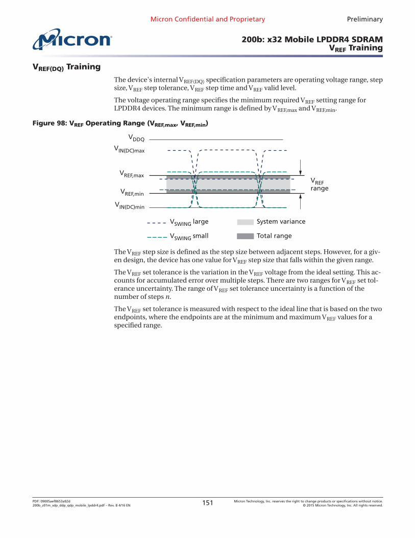
VREF(DQ) Training
The device's internal VREF(DQ) specification parameters are operating voltage range, stepsize, VREF step tolerance, VREF step time and VREF valid level.
The voltage operating range specifies the minimum required VREF setting range forLPDDR4 devices. The minimum range is defined by VREF,max and VREF,min.
Figure 98: VREF Operating Range (VREF,max, VREF,min)
VREF,maxVREFrange
VSWING large System variance
Total rangeVSWING small
VREF,min
VIN(DC)min
VIN(DC)max
VDDQ
The VREF step size is defined as the step size between adjacent steps. However, for a giv-en design, the device has one value for VREF step size that falls within the given range.
The VREF set tolerance is the variation in the VREF voltage from the ideal setting. This ac-counts for accumulated error over multiple steps. There are two ranges for VREF set tol-erance uncertainty. The range of VREF set tolerance uncertainty is a function of thenumber of steps n.
The VREF set tolerance is measured with respect to the ideal line that is based on the twoendpoints, where the endpoints are at the minimum and maximum VREF values for aspecified range.
Micron Confidential and Proprietary Preliminary
200b: x32 Mobile LPDDR4 SDRAMVREF Training
PDF: 09005aef8653a92d200b_z01m_sdp_ddp_qdp_mobile_lpddr4.pdf – Rev. B 4/16 EN 151 Micron Technology, Inc. reserves the right to change products or specifications without notice.
© 2015 Micron Technology, Inc. All rights reserved.
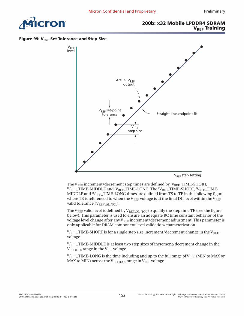
Figure 99: VREF Set Tolerance and Step Size
VREFlevel
VREF step setting
Actual VREFoutput
VREF set-pointtolerance
VREF step size
Straight line endpoint fit
The VREF increment/decrement step times are defined by tVREF_TIME-SHORT,tVREF_TIME-MIDDLE and tVREF_TIME-LONG. The tVREF_TIME-SHORT, tVREF_TIME-MIDDLE and tVREF_TIME-LONG times are defined from TS to TE in the following figurewhere TE is referenced to when the VREF voltage is at the final DC level within the VREFvalid tolerance (VREF,VAL_TOL).
The VREF valid level is defined by VREF,VAL_TOL to qualify the step time TE (see the figurebelow). This parameter is used to ensure an adequate RC time constant behavior of thevoltage level change after any VREF increment/decrement adjustment. This parameter isonly applicable for DRAM component level validation/characterization.
tVREF_TIME-SHORT is for a single step size increment/decrement change in the VREFvoltage.
tVREF_TIME-MIDDLE is at least two step sizes of increment/decrement change in theVREF(DQ) range in the VREFvoltage.
tVREF_TIME-LONG is the time including and up to the full range of VREF (MIN to MAX orMAX to MIN) across the VREF(DQ) range in VREF voltage.
Micron Confidential and Proprietary Preliminary
200b: x32 Mobile LPDDR4 SDRAMVREF Training
PDF: 09005aef8653a92d200b_z01m_sdp_ddp_qdp_mobile_lpddr4.pdf – Rev. B 4/16 EN 152 Micron Technology, Inc. reserves the right to change products or specifications without notice.
© 2015 Micron Technology, Inc. All rights reserved.
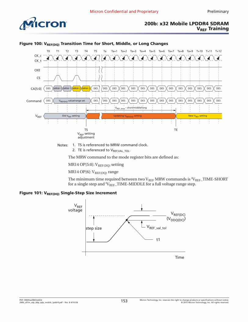
Figure 100: VREF(DQ) Transition Time for Short, Middle, or Long Changes
T0 T1 T2 T3 T4 T5 Ta Ta+1 Ta+2 Ta+3 Ta+4 Ta+5 Ta+6 Ta+7 Ta+8 Ta+9 T+10 T+11 T+12
CK_c
CK_t
CA[5:0]
Command
TSVREF settingadjustment
TE
DES
DES VREF(DQ) value/range set
VREF Old VREF setting Updating VREF(DQ) setting New VREF setting
MRW-1 DESDES DES DES DESMRW-1 MRW-2 MRW-2 DES DES DES DES DES DES DES DES
DESDES DES DES DES DES DES DES DES DES DES DES
DES
DES DES
CS
CKE
VREF_time – short/middle/long
Notes: 1. TS is referenced to MRW command clock.2. TE is referenced to VREF,VAL_TOL.
The MRW command to the mode register bits are defined as:
MR14 OP[5:0]: VREF(DQ) setting
MR14 OP[6]: VREF(DQ) range
The minimum time required between two VREF MRW commands is tVREF_TIME-SHORTfor a single step and tVREF_TIME-MIDDLE for a full voltage range step.
Figure 101: VREF(DQ) Single-Step Size Increment
VREFvoltage
Time
VREF(DC)(V )DDQ(DC)
t1
step size VREF_val_tol
Micron Confidential and Proprietary Preliminary
200b: x32 Mobile LPDDR4 SDRAMVREF Training
PDF: 09005aef8653a92d200b_z01m_sdp_ddp_qdp_mobile_lpddr4.pdf – Rev. B 4/16 EN 153 Micron Technology, Inc. reserves the right to change products or specifications without notice.
© 2015 Micron Technology, Inc. All rights reserved.
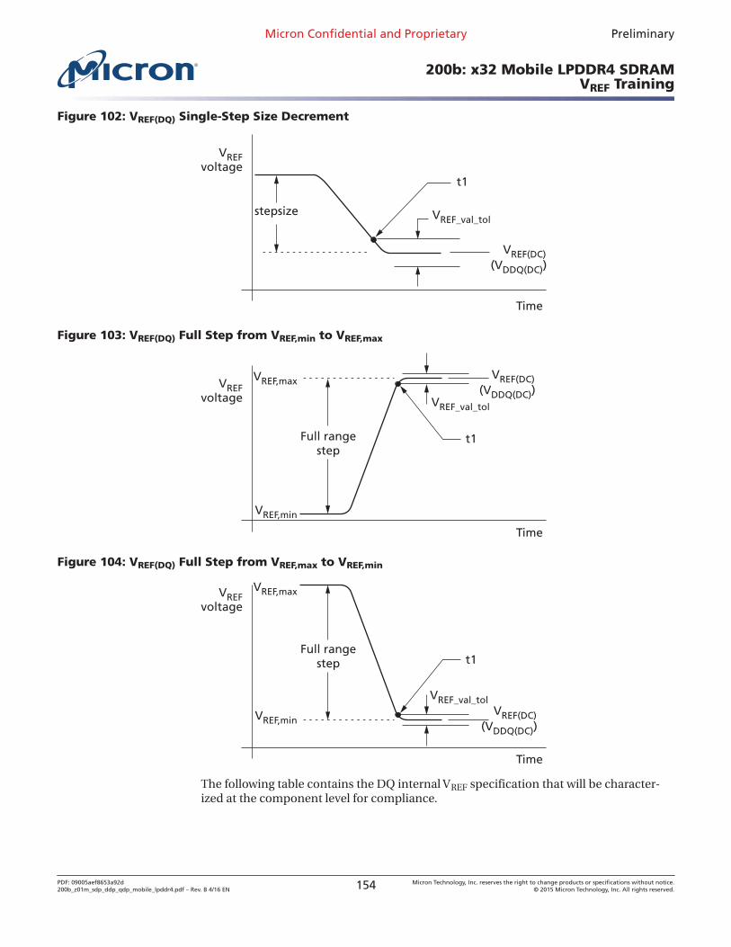
Figure 102: VREF(DQ) Single-Step Size Decrement
VREFvoltage
Time
t1
stepsize VREF_val_tol
VREF(DC)(V )DDQ(DC)
Figure 103: VREF(DQ) Full Step from VREF,min to VREF,max
VREFvoltage
VREF,max
VREF,min
Time
t1Full rangestep
VREF_val_tol
VREF(DC)(V )DDQ(DC)
Figure 104: VREF(DQ) Full Step from VREF,max to VREF,min
VREFvoltage
VREF,max
VREF,min
Time
t1Full range
step
VREF_val_tolVREF(DC)
(V )DDQ(DC)
The following table contains the DQ internal VREF specification that will be character-ized at the component level for compliance.
Micron Confidential and Proprietary Preliminary
200b: x32 Mobile LPDDR4 SDRAMVREF Training
PDF: 09005aef8653a92d200b_z01m_sdp_ddp_qdp_mobile_lpddr4.pdf – Rev. B 4/16 EN 154 Micron Technology, Inc. reserves the right to change products or specifications without notice.
© 2015 Micron Technology, Inc. All rights reserved.
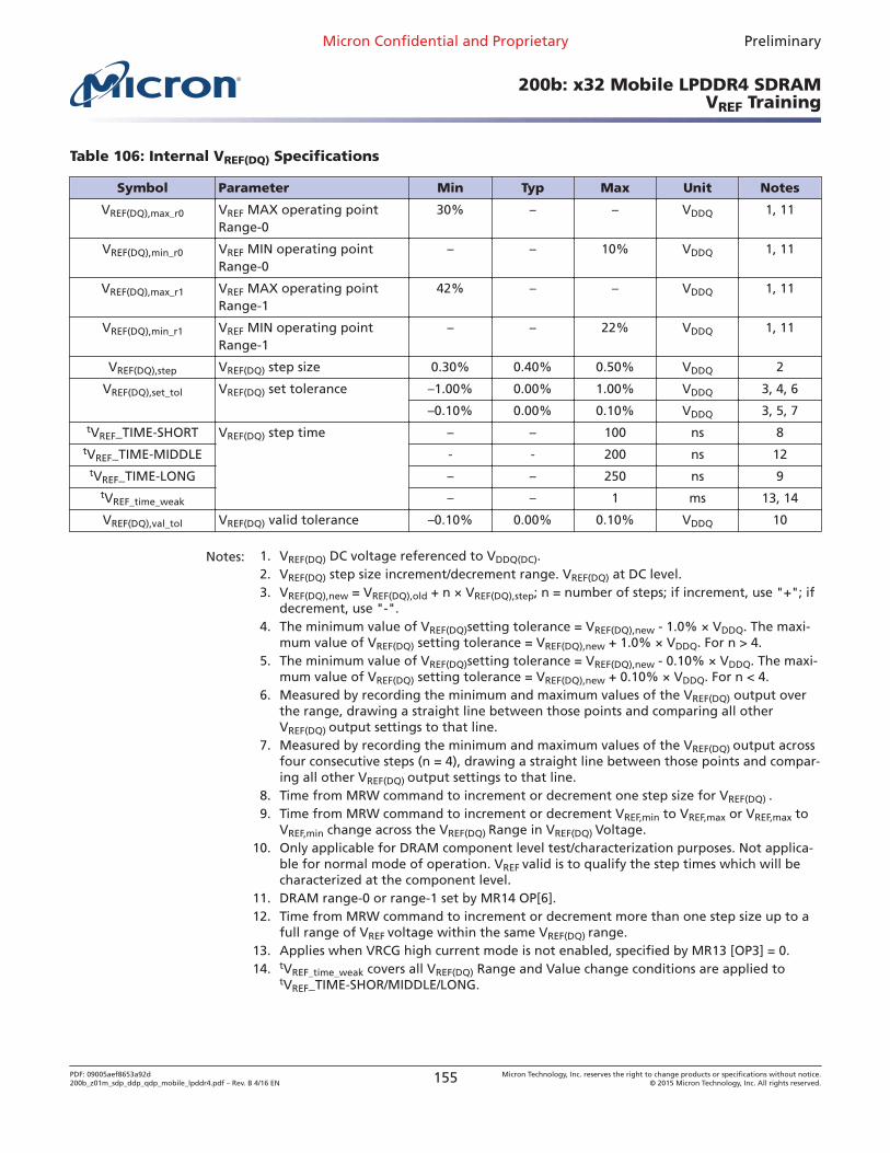
Table 106: Internal VREF(DQ) Specifications
Symbol Parameter Min Typ Max Unit Notes
VREF(DQ),max_r0 VREF MAX operating pointRange-0
30% – – VDDQ 1, 11
VREF(DQ),min_r0 VREF MIN operating pointRange-0
– – 10% VDDQ 1, 11
VREF(DQ),max_r1 VREF MAX operating pointRange-1
42% – – VDDQ 1, 11
VREF(DQ),min_r1 VREF MIN operating pointRange-1
– – 22% VDDQ 1, 11
VREF(DQ),step VREF(DQ) step size 0.30% 0.40% 0.50% VDDQ 2
VREF(DQ),set_tol VREF(DQ) set tolerance –1.00% 0.00% 1.00% VDDQ 3, 4, 6
–0.10% 0.00% 0.10% VDDQ 3, 5, 7tVREF_TIME-SHORT VREF(DQ) step time – – 100 ns 8
tVREF_TIME-MIDDLE - - 200 ns 12tVREF_TIME-LONG – – 250 ns 9
tVREF_time_weak – – 1 ms 13, 14
VREF(DQ),val_tol VREF(DQ) valid tolerance –0.10% 0.00% 0.10% VDDQ 10
Notes: 1. VREF(DQ) DC voltage referenced to VDDQ(DC).2. VREF(DQ) step size increment/decrement range. VREF(DQ) at DC level.3. VREF(DQ),new = VREF(DQ),old + n × VREF(DQ),step; n = number of steps; if increment, use "+"; if
decrement, use "-".4. The minimum value of VREF(DQ)setting tolerance = VREF(DQ),new - 1.0% × VDDQ. The maxi-
mum value of VREF(DQ) setting tolerance = VREF(DQ),new + 1.0% × VDDQ. For n > 4.5. The minimum value of VREF(DQ)setting tolerance = VREF(DQ),new - 0.10% × VDDQ. The maxi-
mum value of VREF(DQ) setting tolerance = VREF(DQ),new + 0.10% × VDDQ. For n < 4.6. Measured by recording the minimum and maximum values of the VREF(DQ) output over
the range, drawing a straight line between those points and comparing all otherVREF(DQ) output settings to that line.
7. Measured by recording the minimum and maximum values of the VREF(DQ) output acrossfour consecutive steps (n = 4), drawing a straight line between those points and compar-ing all other VREF(DQ) output settings to that line.
8. Time from MRW command to increment or decrement one step size for VREF(DQ) .9. Time from MRW command to increment or decrement VREF,min to VREF,max or VREF,max to
VREF,min change across the VREF(DQ) Range in VREF(DQ) Voltage.10. Only applicable for DRAM component level test/characterization purposes. Not applica-
ble for normal mode of operation. VREF valid is to qualify the step times which will becharacterized at the component level.
11. DRAM range-0 or range-1 set by MR14 OP[6].12. Time from MRW command to increment or decrement more than one step size up to a
full range of VREF voltage within the same VREF(DQ) range.13. Applies when VRCG high current mode is not enabled, specified by MR13 [OP3] = 0.14. tVREF_time_weak covers all VREF(DQ) Range and Value change conditions are applied to
tVREF_TIME-SHOR/MIDDLE/LONG.
Micron Confidential and Proprietary Preliminary
200b: x32 Mobile LPDDR4 SDRAMVREF Training
PDF: 09005aef8653a92d200b_z01m_sdp_ddp_qdp_mobile_lpddr4.pdf – Rev. B 4/16 EN 155 Micron Technology, Inc. reserves the right to change products or specifications without notice.
© 2015 Micron Technology, Inc. All rights reserved.
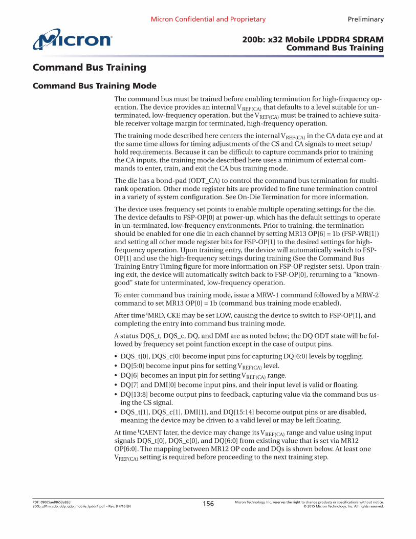
Command Bus Training
Command Bus Training Mode
The command bus must be trained before enabling termination for high-frequency op-eration. The device provides an internal VREF(CA) that defaults to a level suitable for un-terminated, low-frequency operation, but the VREF(CA) must be trained to achieve suita-ble receiver voltage margin for terminated, high-frequency operation.
The training mode described here centers the internal VREF(CA) in the CA data eye and atthe same time allows for timing adjustments of the CS and CA signals to meet setup/hold requirements. Because it can be difficult to capture commands prior to trainingthe CA inputs, the training mode described here uses a minimum of external com-mands to enter, train, and exit the CA bus training mode.
The die has a bond-pad (ODT_CA) to control the command bus termination for multi-rank operation. Other mode register bits are provided to fine tune termination controlin a variety of system configuration. See On-Die Termination for more information.
The device uses frequency set points to enable multiple operating settings for the die.The device defaults to FSP-OP[0] at power-up, which has the default settings to operatein un-terminated, low-frequency environments. Prior to training, the terminationshould be enabled for one die in each channel by setting MR13 OP[6] = 1b (FSP-WR[1])and setting all other mode register bits for FSP-OP[1] to the desired settings for high-frequency operation. Upon training entry, the device will automatically switch to FSP-OP[1] and use the high-frequency settings during training (See the Command BusTraining Entry Timing figure for more information on FSP-OP register sets). Upon train-ing exit, the device will automatically switch back to FSP-OP[0], returning to a "known-good" state for unterminated, low-frequency operation.
To enter command bus training mode, issue a MRW-1 command followed by a MRW-2command to set MR13 OP[0] = 1b (command bus training mode enabled).
After time tMRD, CKE may be set LOW, causing the device to switch to FSP-OP[1], andcompleting the entry into command bus training mode.
A status DQS_t, DQS_c, DQ, and DMI are as noted below; the DQ ODT state will be fol-lowed by frequency set point function except in the case of output pins.
• DQS_t[0], DQS_c[0] become input pins for capturing DQ[6:0] levels by toggling.• DQ[5:0] become input pins for setting VREF(CA) level.• DQ[6] becomes an input pin for setting VREF(CA) range.• DQ[7] and DMI[0] become input pins, and their input level is valid or floating.• DQ[13:8] become output pins to feedback, capturing value via the command bus us-
ing the CS signal.• DQS_t[1], DQS_c[1], DMI[1], and DQ[15:14] become output pins or are disabled,
meaning the device may be driven to a valid level or may be left floating.
At time tCAENT later, the device may change its VREF(CA) range and value using inputsignals DQS_t[0], DQS_c[0], and DQ[6:0] from existing value that is set via MR12OP[6:0]. The mapping between MR12 OP code and DQs is shown below. At least oneVREF(CA) setting is required before proceeding to the next training step.
Micron Confidential and Proprietary Preliminary
200b: x32 Mobile LPDDR4 SDRAMCommand Bus Training
PDF: 09005aef8653a92d200b_z01m_sdp_ddp_qdp_mobile_lpddr4.pdf – Rev. B 4/16 EN 156 Micron Technology, Inc. reserves the right to change products or specifications without notice.
© 2015 Micron Technology, Inc. All rights reserved.
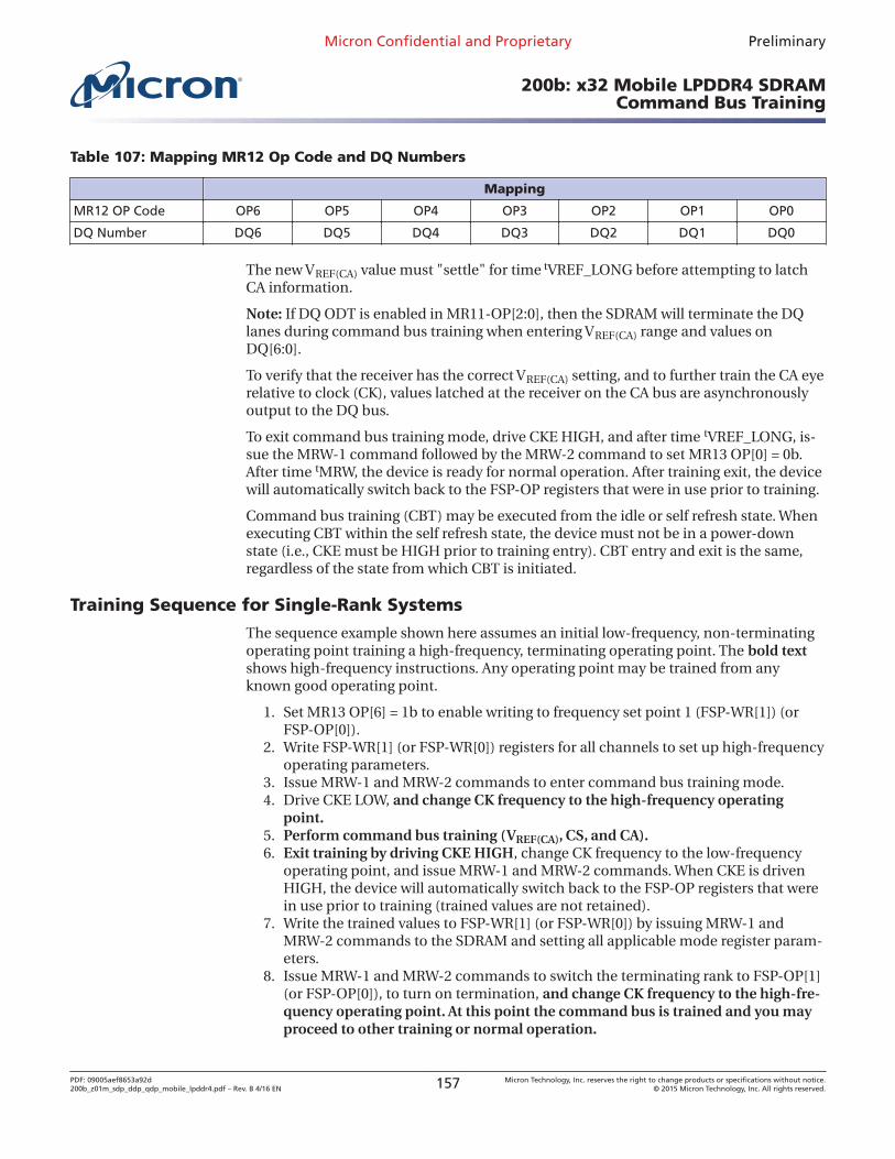
Table 107: Mapping MR12 Op Code and DQ Numbers
Mapping
MR12 OP Code OP6 OP5 OP4 OP3 OP2 OP1 OP0
DQ Number DQ6 DQ5 DQ4 DQ3 DQ2 DQ1 DQ0
The new VREF(CA) value must "settle" for time tVREF_LONG before attempting to latchCA information.
Note: If DQ ODT is enabled in MR11-OP[2:0], then the SDRAM will terminate the DQlanes during command bus training when entering VREF(CA) range and values onDQ[6:0].
To verify that the receiver has the correct VREF(CA) setting, and to further train the CA eyerelative to clock (CK), values latched at the receiver on the CA bus are asynchronouslyoutput to the DQ bus.
To exit command bus training mode, drive CKE HIGH, and after time tVREF_LONG, is-sue the MRW-1 command followed by the MRW-2 command to set MR13 OP[0] = 0b.After time tMRW, the device is ready for normal operation. After training exit, the devicewill automatically switch back to the FSP-OP registers that were in use prior to training.
Command bus training (CBT) may be executed from the idle or self refresh state. Whenexecuting CBT within the self refresh state, the device must not be in a power-downstate (i.e., CKE must be HIGH prior to training entry). CBT entry and exit is the same,regardless of the state from which CBT is initiated.
Training Sequence for Single-Rank Systems
The sequence example shown here assumes an initial low-frequency, non-terminatingoperating point training a high-frequency, terminating operating point. The bold textshows high-frequency instructions. Any operating point may be trained from anyknown good operating point.
1. Set MR13 OP[6] = 1b to enable writing to frequency set point 1 (FSP-WR[1]) (orFSP-OP[0]).
2. Write FSP-WR[1] (or FSP-WR[0]) registers for all channels to set up high-frequencyoperating parameters.
3. Issue MRW-1 and MRW-2 commands to enter command bus training mode.4. Drive CKE LOW, and change CK frequency to the high-frequency operating
point.5. Perform command bus training (VREF(CA), CS, and CA).6. Exit training by driving CKE HIGH, change CK frequency to the low-frequency
operating point, and issue MRW-1 and MRW-2 commands. When CKE is drivenHIGH, the device will automatically switch back to the FSP-OP registers that werein use prior to training (trained values are not retained).
7. Write the trained values to FSP-WR[1] (or FSP-WR[0]) by issuing MRW-1 andMRW-2 commands to the SDRAM and setting all applicable mode register param-eters.
8. Issue MRW-1 and MRW-2 commands to switch the terminating rank to FSP-OP[1](or FSP-OP[0]), to turn on termination, and change CK frequency to the high-fre-quency operating point. At this point the command bus is trained and you mayproceed to other training or normal operation.
Micron Confidential and Proprietary Preliminary
200b: x32 Mobile LPDDR4 SDRAMCommand Bus Training
PDF: 09005aef8653a92d200b_z01m_sdp_ddp_qdp_mobile_lpddr4.pdf – Rev. B 4/16 EN 157 Micron Technology, Inc. reserves the right to change products or specifications without notice.
© 2015 Micron Technology, Inc. All rights reserved.
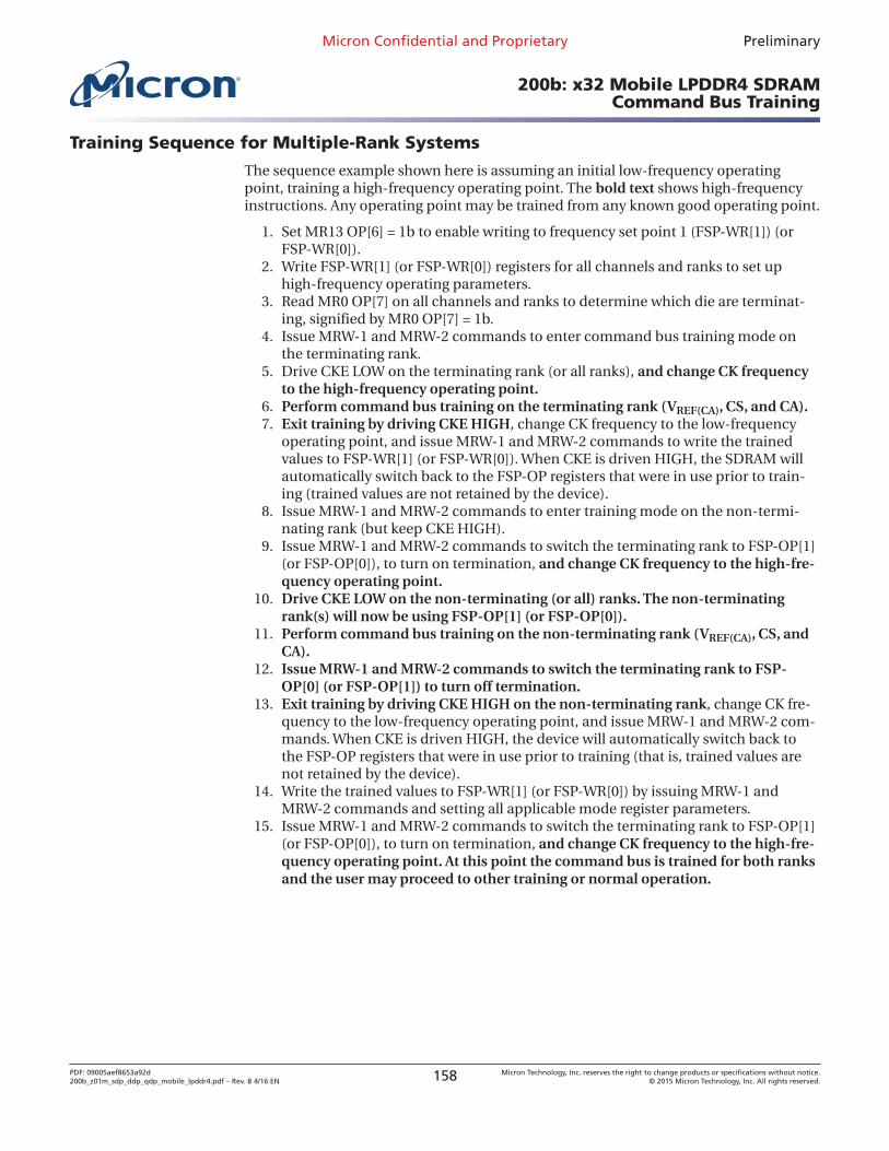
Training Sequence for Multiple-Rank Systems
The sequence example shown here is assuming an initial low-frequency operatingpoint, training a high-frequency operating point. The bold text shows high-frequencyinstructions. Any operating point may be trained from any known good operating point.
1. Set MR13 OP[6] = 1b to enable writing to frequency set point 1 (FSP-WR[1]) (orFSP-WR[0]).
2. Write FSP-WR[1] (or FSP-WR[0]) registers for all channels and ranks to set uphigh-frequency operating parameters.
3. Read MR0 OP[7] on all channels and ranks to determine which die are terminat-ing, signified by MR0 OP[7] = 1b.
4. Issue MRW-1 and MRW-2 commands to enter command bus training mode onthe terminating rank.
5. Drive CKE LOW on the terminating rank (or all ranks), and change CK frequencyto the high-frequency operating point.
6. Perform command bus training on the terminating rank (VREF(CA), CS, and CA).7. Exit training by driving CKE HIGH, change CK frequency to the low-frequency
operating point, and issue MRW-1 and MRW-2 commands to write the trainedvalues to FSP-WR[1] (or FSP-WR[0]). When CKE is driven HIGH, the SDRAM willautomatically switch back to the FSP-OP registers that were in use prior to train-ing (trained values are not retained by the device).
8. Issue MRW-1 and MRW-2 commands to enter training mode on the non-termi-nating rank (but keep CKE HIGH).
9. Issue MRW-1 and MRW-2 commands to switch the terminating rank to FSP-OP[1](or FSP-OP[0]), to turn on termination, and change CK frequency to the high-fre-quency operating point.
10. Drive CKE LOW on the non-terminating (or all) ranks. The non-terminatingrank(s) will now be using FSP-OP[1] (or FSP-OP[0]).
11. Perform command bus training on the non-terminating rank (VREF(CA), CS, andCA).
12. Issue MRW-1 and MRW-2 commands to switch the terminating rank to FSP-OP[0] (or FSP-OP[1]) to turn off termination.
13. Exit training by driving CKE HIGH on the non-terminating rank, change CK fre-quency to the low-frequency operating point, and issue MRW-1 and MRW-2 com-mands. When CKE is driven HIGH, the device will automatically switch back tothe FSP-OP registers that were in use prior to training (that is, trained values arenot retained by the device).
14. Write the trained values to FSP-WR[1] (or FSP-WR[0]) by issuing MRW-1 andMRW-2 commands and setting all applicable mode register parameters.
15. Issue MRW-1 and MRW-2 commands to switch the terminating rank to FSP-OP[1](or FSP-OP[0]), to turn on termination, and change CK frequency to the high-fre-quency operating point. At this point the command bus is trained for both ranksand the user may proceed to other training or normal operation.
Micron Confidential and Proprietary Preliminary
200b: x32 Mobile LPDDR4 SDRAMCommand Bus Training
PDF: 09005aef8653a92d200b_z01m_sdp_ddp_qdp_mobile_lpddr4.pdf – Rev. B 4/16 EN 158 Micron Technology, Inc. reserves the right to change products or specifications without notice.
© 2015 Micron Technology, Inc. All rights reserved.
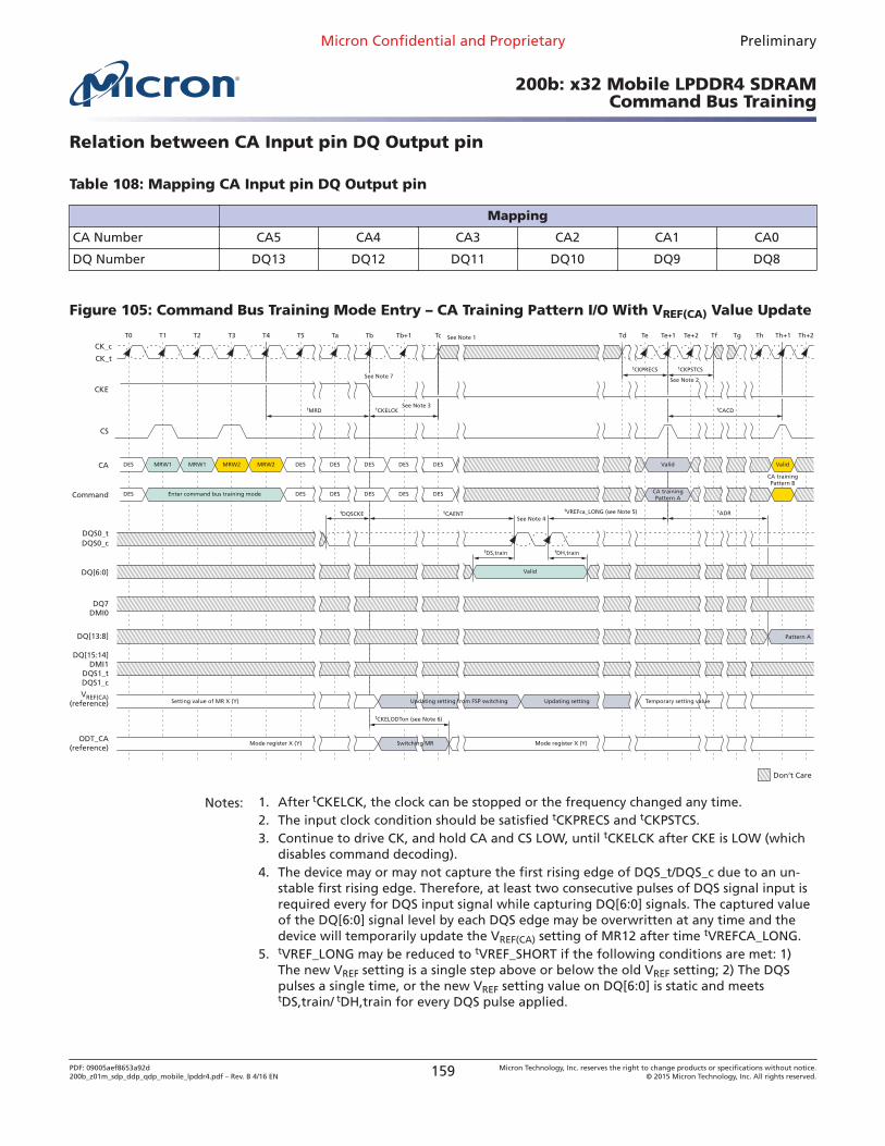
Relation between CA Input pin DQ Output pin
Table 108: Mapping CA Input pin DQ Output pin
Mapping
CA Number CA5 CA4 CA3 CA2 CA1 CA0
DQ Number DQ13 DQ12 DQ11 DQ10 DQ9 DQ8
Figure 105: Command Bus Training Mode Entry – CA Training Pattern I/O With VREF(CA) Value Update
CS
T0 T1 T2 T3 T4 T5 Ta Tb+1Tb Tc
CK_c
CK_t
Td ThTf Tg Th+2Th+1Te Te+2Te+1
CA
Command
CKE
See Note 1
tMRD
tCKPRECS tCKPSTCS
tCACD
MRW2 DES
DES
Setting value of MR X (Y) Updating setting
Mode register X (Y)
Updating setting from FSP switching
Switching MR
Temporary setting value
DES
DES
DES
DES
DES
DES
DES
DES
DES
DES
MRW2MRW1MRW1
Enter command bus training mode
DQS0_tDQS0_c
DQ[6:0]
VREF(CA)(reference)
DQ7DMI0
Valid
Don’t Care
tADRtVREFca_LONG (see Note 5)
Valid
ODT_CA(reference)
Valid
CA trainingPattern A
CA trainingPattern B
Pattern A
See Note 3
See Note 4
See Note 7
tCKELCK
tDQSCKE
tCKELODTon (see Note 6)
tCAENT
DQ[13:8]
DQ[15:14]DMI1
DQS1_tDQS1_c
See Note 2
tDS,train tDH,train
Mode register X (Y)
Notes: 1. After tCKELCK, the clock can be stopped or the frequency changed any time.2. The input clock condition should be satisfied tCKPRECS and tCKPSTCS.3. Continue to drive CK, and hold CA and CS LOW, until tCKELCK after CKE is LOW (which
disables command decoding).4. The device may or may not capture the first rising edge of DQS_t/DQS_c due to an un-
stable first rising edge. Therefore, at least two consecutive pulses of DQS signal input isrequired every for DQS input signal while capturing DQ[6:0] signals. The captured valueof the DQ[6:0] signal level by each DQS edge may be overwritten at any time and thedevice will temporarily update the VREF(CA) setting of MR12 after time tVREFCA_LONG.
5. tVREF_LONG may be reduced to tVREF_SHORT if the following conditions are met: 1)The new VREF setting is a single step above or below the old VREF setting; 2) The DQSpulses a single time, or the new VREF setting value on DQ[6:0] is static and meetstDS,train/ tDH,train for every DQS pulse applied.
Micron Confidential and Proprietary Preliminary
200b: x32 Mobile LPDDR4 SDRAMCommand Bus Training
PDF: 09005aef8653a92d200b_z01m_sdp_ddp_qdp_mobile_lpddr4.pdf – Rev. B 4/16 EN 159 Micron Technology, Inc. reserves the right to change products or specifications without notice.
© 2015 Micron Technology, Inc. All rights reserved.
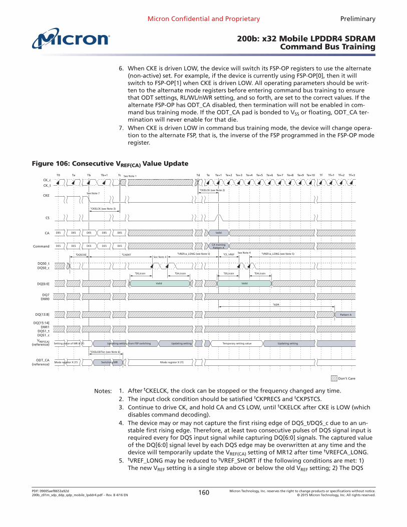
6. When CKE is driven LOW, the device will switch its FSP-OP registers to use the alternate(non-active) set. For example, if the device is currently using FSP-OP[0], then it willswitch to FSP-OP[1] when CKE is driven LOW. All operating parameters should be writ-ten to the alternate mode registers before entering command bus training to ensurethat ODT settings, RL/WL/nWR setting, and so forth, are set to the correct values. If thealternate FSP-OP has ODT_CA disabled, then termination will not be enabled in com-mand bus training mode. If the ODT_CA pad is bonded to VSS or floating, ODT_CA ter-mination will never enable for that die.
7. When CKE is driven LOW in command bus training mode, the device will change opera-tion to the alternate FSP, that is, the inverse of the FSP programmed in the FSP-OP moderegister.
Figure 106: Consecutive VREF(CA) Value Update
CS
T0 Ta Tb+1Tb Tc
CK_c
CK_t
Td Tf+2Tf Tf+1 Tf+3Te Te+2Te+1 Te+4Te+3 Te+6Te+5 Te+8Te+7 Te+10Te+9
CA
Command
CKE
See Note 1
Updating setting Updating setting
Mode register X (Y)
Updating setting from FSP switching
Switching MR
Temporary setting value
DES
DES
DES
DES
DES
DES
DES
DES
DES
DES
DQS0_tDQS0_c
DQ[6:0]
VREF(CA)(reference)
DQ7DMI0
Don’t Care
tADR
tVREFca_LONG (see Note 5) tVREFca_LONG (see Note 5)
Valid
ODT_CA(reference)
Valid
CA trainingPattern A
Pattern A
See Note 4
See Note 4
See Note 7
tCKELCK (see Note 3)
tDQSCKE
tCKELODTon (see Note 6)
tCAENT
DQ[13:8]
DQ[15:14]DMI1
DQS1_tDQS1_c
tDS,train tDH,train
Mode register X (Y)
Valid
tDS,train
tCS_VREF
tDH,train
tCKELCK (see Note 2)
Setting value of MR X (Y)
Notes: 1. After tCKELCK, the clock can be stopped or the frequency changed any time.2. The input clock condition should be satisfied tCKPRECS and tCKPSTCS.3. Continue to drive CK, and hold CA and CS LOW, until tCKELCK after CKE is LOW (which
disables command decoding).4. The device may or may not capture the first rising edge of DQS_t/DQS_c due to an un-
stable first rising edge. Therefore, at least two consecutive pulses of DQS signal input isrequired every for DQS input signal while capturing DQ[6:0] signals. The captured valueof the DQ[6:0] signal level by each DQS edge may be overwritten at any time and thedevice will temporarily update the VREF(CA) setting of MR12 after time tVREFCA_LONG.
5. tVREF_LONG may be reduced to tVREF_SHORT if the following conditions are met: 1)The new VREF setting is a single step above or below the old VREF setting; 2) The DQS
Micron Confidential and Proprietary Preliminary
200b: x32 Mobile LPDDR4 SDRAMCommand Bus Training
PDF: 09005aef8653a92d200b_z01m_sdp_ddp_qdp_mobile_lpddr4.pdf – Rev. B 4/16 EN 160 Micron Technology, Inc. reserves the right to change products or specifications without notice.
© 2015 Micron Technology, Inc. All rights reserved.
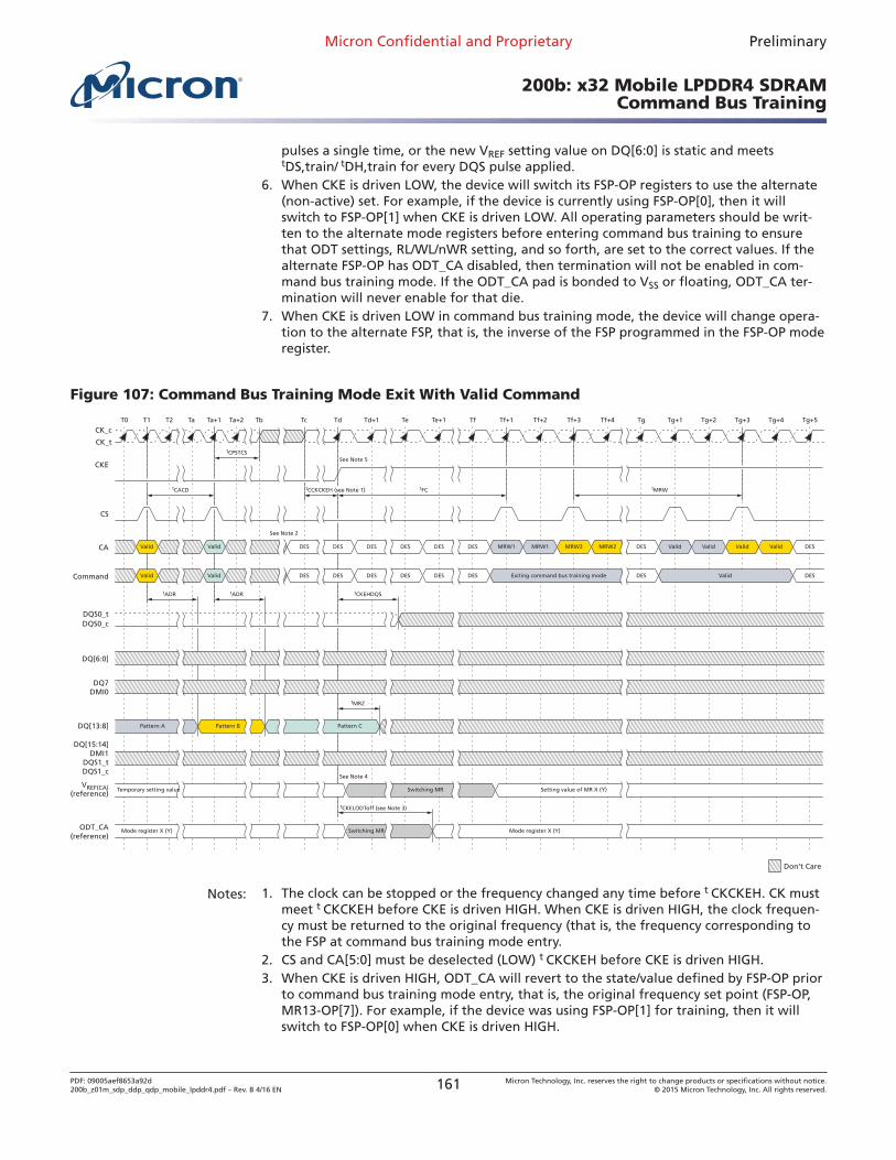
pulses a single time, or the new VREF setting value on DQ[6:0] is static and meetstDS,train/ tDH,train for every DQS pulse applied.
6. When CKE is driven LOW, the device will switch its FSP-OP registers to use the alternate(non-active) set. For example, if the device is currently using FSP-OP[0], then it willswitch to FSP-OP[1] when CKE is driven LOW. All operating parameters should be writ-ten to the alternate mode registers before entering command bus training to ensurethat ODT settings, RL/WL/nWR setting, and so forth, are set to the correct values. If thealternate FSP-OP has ODT_CA disabled, then termination will not be enabled in com-mand bus training mode. If the ODT_CA pad is bonded to VSS or floating, ODT_CA ter-mination will never enable for that die.
7. When CKE is driven LOW in command bus training mode, the device will change opera-tion to the alternate FSP, that is, the inverse of the FSP programmed in the FSP-OP moderegister.
Figure 107: Command Bus Training Mode Exit With Valid Command
T0 T1 Ta+1 Ta+2TaT2 Tb Tc Td Td+1 Te Te+1 Tf Tf+1 Tf+2 Tf+3 Tf+4 Tg Tg+1 Tg+2 Tg+3 Tg+4 Tg+5
CK_c
CK_t
CS
CA
Command
CKE
Setting value of MR X (Y)
Mode register X (Y)
Switching MR
Valid
Valid
Valid
Valid
DES
DES
Pattern CPattern BPattern A
DES
DES
DES
DES
DES
DES
DES
DES
DES
DES
DES
DES
DES
DES
MRW1 Valid Valid Valid ValidMRW1 MRW2 MRW2
Exiting command bus training mode
DQS0_tDQS0_c
DQ[6:0]
VREF(CA)(reference)
DQ7DMI0
Don’t Care
ODT_CA(reference)
See Note 5
See Note 2
tCPSTCS
tCKELODToff (see Note 3)
See Note 4
DQ[13:8]
DQ[15:14]DMI1
DQS1_tDQS1_c
Mode register X (Y)
tADR tADR tCKEHDQS
tMRZ
tCACD tCCKCKEH (see Note 1) tFC tMRW
Valid
Switching MR
Temporary setting value
Notes: 1. The clock can be stopped or the frequency changed any time before t CKCKEH. CK mustmeet t CKCKEH before CKE is driven HIGH. When CKE is driven HIGH, the clock frequen-cy must be returned to the original frequency (that is, the frequency corresponding tothe FSP at command bus training mode entry.
2. CS and CA[5:0] must be deselected (LOW) t CKCKEH before CKE is driven HIGH.3. When CKE is driven HIGH, ODT_CA will revert to the state/value defined by FSP-OP prior
to command bus training mode entry, that is, the original frequency set point (FSP-OP,MR13-OP[7]). For example, if the device was using FSP-OP[1] for training, then it willswitch to FSP-OP[0] when CKE is driven HIGH.
Micron Confidential and Proprietary Preliminary
200b: x32 Mobile LPDDR4 SDRAMCommand Bus Training
PDF: 09005aef8653a92d200b_z01m_sdp_ddp_qdp_mobile_lpddr4.pdf – Rev. B 4/16 EN 161 Micron Technology, Inc. reserves the right to change products or specifications without notice.
© 2015 Micron Technology, Inc. All rights reserved.
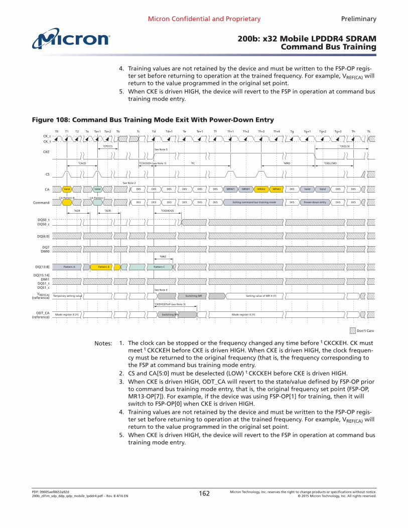
4. Training values are not retained by the device and must be written to the FSP-OP regis-ter set before returning to operation at the trained frequency. For example, VREF(CA) willreturn to the value programmed in the original set point.
5. When CKE is driven HIGH, the device will revert to the FSP in operation at command bustraining mode entry.
Figure 108: Command Bus Training Mode Exit With Power-Down Entry
T0 T1 Ta+1 Ta+2TaT2 Tb Tc Td Td+1 Te Te+1 Tf Tf+1 Tf+2 Tf+3 Tf+4 Tg Tg+1 Tg+2 Tg+3 Th Tk
CK_c
CK_t
CS
CA
Command
CKE
Setting value of MR X (Y)
Mode register X (Y)
Switching MR
Valid
CA Pattern B CA Pattern C
Valid DES
DES
Pattern CPattern BPattern A
DES
DES
DES
DES
DES
DES
DES
DES
DES DES DES
DES
DES
DES
MRW1 Valid Valid
DES DES
MRW1 MRW2 MRW2
Exiting command bus training mode
DQS0_tDQS0_c
DQ[6:0]
VREF(CA)(reference)
DQ7DMI0
Don’t Care
ODT_CA(reference)
See Note 5
See Note 2
tCPSTCS tCKELCK
tCKEHODToff (see Note 3)
See Note 4
DQ[13:8]
DQ[15:14]DMI1
DQS1_tDQS1_c
Mode register X (Y)
tADR tADR tCKEHDQS
tMRZ
tCACD tCCKCKEH (see Note 1) tFC tMRD tCKELCMD
Switching MR
Temporary setting value
Power-down entry
Notes: 1. The clock can be stopped or the frequency changed any time before t CKCKEH. CK mustmeet t CKCKEH before CKE is driven HIGH. When CKE is driven HIGH, the clock frequen-cy must be returned to the original frequency (that is, the frequency corresponding tothe FSP at command bus training mode entry.
2. CS and CA[5:0] must be deselected (LOW) t CKCKEH before CKE is driven HIGH.3. When CKE is driven HIGH, ODT_CA will revert to the state/value defined by FSP-OP prior
to command bus training mode entry, that is, the original frequency set point (FSP-OP,MR13-OP[7]). For example, if the device was using FSP-OP[1] for training, then it willswitch to FSP-OP[0] when CKE is driven HIGH.
4. Training values are not retained by the device and must be written to the FSP-OP regis-ter set before returning to operation at the trained frequency. For example, VREF(CA) willreturn to the value programmed in the original set point.
5. When CKE is driven HIGH, the device will revert to the FSP in operation at command bustraining mode entry.
Micron Confidential and Proprietary Preliminary
200b: x32 Mobile LPDDR4 SDRAMCommand Bus Training
PDF: 09005aef8653a92d200b_z01m_sdp_ddp_qdp_mobile_lpddr4.pdf – Rev. B 4/16 EN 162 Micron Technology, Inc. reserves the right to change products or specifications without notice.
© 2015 Micron Technology, Inc. All rights reserved.
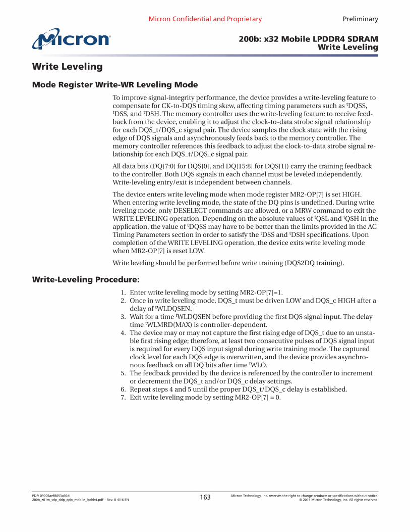
Write Leveling
Mode Register Write-WR Leveling Mode
To improve signal-integrity performance, the device provides a write-leveling feature tocompensate for CK-to-DQS timing skew, affecting timing parameters such as tDQSS,tDSS, and tDSH. The memory controller uses the write-leveling feature to receive feed-back from the device, enabling it to adjust the clock-to-data strobe signal relationshipfor each DQS_t/DQS_c signal pair. The device samples the clock state with the risingedge of DQS signals and asynchronously feeds back to the memory controller. Thememory controller references this feedback to adjust the clock-to-data strobe signal re-lationship for each DQS_t/DQS_c signal pair.
All data bits (DQ[7:0] for DQS[0], and DQ[15:8] for DQS[1]) carry the training feedbackto the controller. Both DQS signals in each channel must be leveled independently.Write-leveling entry/exit is independent between channels.
The device enters write leveling mode when mode register MR2-OP[7] is set HIGH.When entering write leveling mode, the state of the DQ pins is undefined. During writeleveling mode, only DESELECT commands are allowed, or a MRW command to exit theWRITE LEVELING operation. Depending on the absolute values of tQSL and tQSH in theapplication, the value of tDQSS may have to be better than the limits provided in the ACTiming Parameters section in order to satisfy the tDSS and tDSH specifications. Uponcompletion of the WRITE LEVELING operation, the device exits write leveling modewhen MR2-OP[7] is reset LOW.
Write leveling should be performed before write training (DQS2DQ training).
Write-Leveling Procedure:
1. Enter write leveling mode by setting MR2-OP[7]=1.2. Once in write leveling mode, DQS_t must be driven LOW and DQS_c HIGH after a
delay of tWLDQSEN.3. Wait for a time tWLDQSEN before providing the first DQS signal input. The delay
time tWLMRD(MAX) is controller-dependent.4. The device may or may not capture the first rising edge of DQS_t due to an unsta-
ble first rising edge; therefore, at least two consecutive pulses of DQS signal inputis required for every DQS input signal during write training mode. The capturedclock level for each DQS edge is overwritten, and the device provides asynchro-nous feedback on all DQ bits after time tWLO.
5. The feedback provided by the device is referenced by the controller to incrementor decrement the DQS_t and/or DQS_c delay settings.
6. Repeat steps 4 and 5 until the proper DQS_t/DQS_c delay is established.7. Exit write leveling mode by setting MR2-OP[7] = 0.
Micron Confidential and Proprietary Preliminary
200b: x32 Mobile LPDDR4 SDRAMWrite Leveling
PDF: 09005aef8653a92d200b_z01m_sdp_ddp_qdp_mobile_lpddr4.pdf – Rev. B 4/16 EN 163 Micron Technology, Inc. reserves the right to change products or specifications without notice.
© 2015 Micron Technology, Inc. All rights reserved.
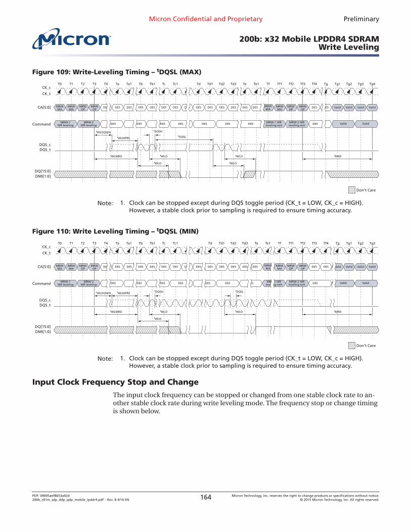
Figure 109: Write-Leveling Timing – tDQSL (MAX)
CK_c
CK_t
CA[5:0]
Command MRW-1WR leveling
DQS_cDQS_t
DQ[15:0]DMI[1:0]
DES DES
DESMRWMA
MRWMA
MRWOP
MRWOP
DES DES DES DES DES DES DES DES DES DES DES DESDES DES DES Valid
DESDES Valid Valid
Valid Valid Valid
tWLDQSENtDQSL
tWLMRD tWLO
tWLO tWLO
tWLO tMRD
tDQSH
DES DES DES DESMRW-2WR leveling
MRW-1 WRleveling exit
MRW-2 WRleveling exit
MRWMA
MRWMA
MRWOP
MRWOP
Don’t Care
T0 T1 T2 T3 T4 Ta Ta1 Tb Tb1 Tc Tc1 Td Td1 Td2 Td3 Te Te1 Tf Tf1 Tf2 Tf3 Tf4 Tg1 Tg2 Tg3 Tg4Tg
tWLWPRE
Note: 1. Clock can be stopped except during DQS toggle period (CK_t = LOW, CK_c = HIGH).However, a stable clock prior to sampling is required to ensure timing accuracy.
Figure 110: Write Leveling Timing – tDQSL (MIN)
CK_c
CK_t
CA[5:0]
Command MRW-1WR leveling
DQS_cDQS_t
DES DES
DESMRWMA
MRWMA
MRWOP
MRWOP
DES DES DES DES DES DES DES DES DES DES DES DES DESDES DES Valid
DESDES Valid Valid
Valid Valid Valid
tWLDQSEN
tWLMRD tWLO
tWLO
tWLO tMRD
tDQSH
DES DES DES DESMRW-2WR leveling
MRW1 WRleveling exit
MRW-2 WRleveling exit
MRWMA
MRWMA
MRWOP
MRWOP
tDQSL
Don’t Care
T0 T1 T2 T3 T4 Ta Ta1 Tb Tb1 Tc Tc1 Td Td1 Td2 Td3 Te Te1 Tf Tf1 Tf2 Tf3 Tf4 Tg1 Tg2 Tg3Tg
tWLWPRE
DQ[15:0]DMI[1:0]
Note: 1. Clock can be stopped except during DQS toggle period (CK_t = LOW, CK_c = HIGH).However, a stable clock prior to sampling is required to ensure timing accuracy.
Input Clock Frequency Stop and Change
The input clock frequency can be stopped or changed from one stable clock rate to an-other stable clock rate during write leveling mode. The frequency stop or change timingis shown below.
Micron Confidential and Proprietary Preliminary
200b: x32 Mobile LPDDR4 SDRAMWrite Leveling
PDF: 09005aef8653a92d200b_z01m_sdp_ddp_qdp_mobile_lpddr4.pdf – Rev. B 4/16 EN 164 Micron Technology, Inc. reserves the right to change products or specifications without notice.
© 2015 Micron Technology, Inc. All rights reserved.
Figure 111: Clock Stop and Timing During Write Leveling
T0 T1 T2 T3 T4CK_c
CK_t
CS
CKE
CA
Command MRW-1WR leveling
MRW-2WR leveling
DQS_cDQS_t
DESELECT DESELECT DESELECT DESELECT DESELECT DESELECT DESELECT DESELECT
MRWMA
MRWMA
MRWOP
MRWOP DES DES DESDESDESDES DESDESDESDESDESDESDESDESDESDES
Ta0 Ta1 Tb0 Tb1 Tb2 Tc0 Td0 Te0 Te1 Tf1Tf0Te4Te3Te2 Tf3Tf2
DES
tWLOtWLO
tWLMRD
tWLWPREtWLDQSEN
tWLO
tCKPRDQStCKPSTDQS
tDQSH tDQSL
tWLO
DQDMI
Table 109: Write Leveling Timing Parameters
Parameter Symbol Min/Max Value Units
DQS_t/DQS_c delay after write levelingmode is programmed
tWLDQSEN MIN 20 tCK
MAX –
Write preamble for write leveling tWLWPRE MIN 20 tCK
MAX –
First DQS_t/DQS_c edge after write level-ing mode is programmed
tWLMRD MIN 40 tCK
MAX –
Write leveling output delay tWLO MIN 0 ns
MAX 20
Mode register set command delay tMRD MIN MAX (14ns, 10nCK) ns
MAX –
Valid clock requirement before DQS tog-gle
tCKPRDQS MIN MAX(7.5ns, 4nCK) –
MAX –
Valid clock requirement after DQS toggle tCKPSTDQS MIN MAX(7.5ns, 4nCK) –
MAX –
Table 110: Write Leveling Setup and Hold Timing
Parameter Symbol Min/Max
Data Rate
Unit1600 2400 3200 3733 4267
Write leveling hold time tWLH MIN 150 100 75 62.5 50 ps
Write leveling setup time tWLS MIN 150 100 75 62.5 50 ps
Micron Confidential and Proprietary Preliminary
200b: x32 Mobile LPDDR4 SDRAMWrite Leveling
PDF: 09005aef8653a92d200b_z01m_sdp_ddp_qdp_mobile_lpddr4.pdf – Rev. B 4/16 EN 165 Micron Technology, Inc. reserves the right to change products or specifications without notice.
© 2015 Micron Technology, Inc. All rights reserved.
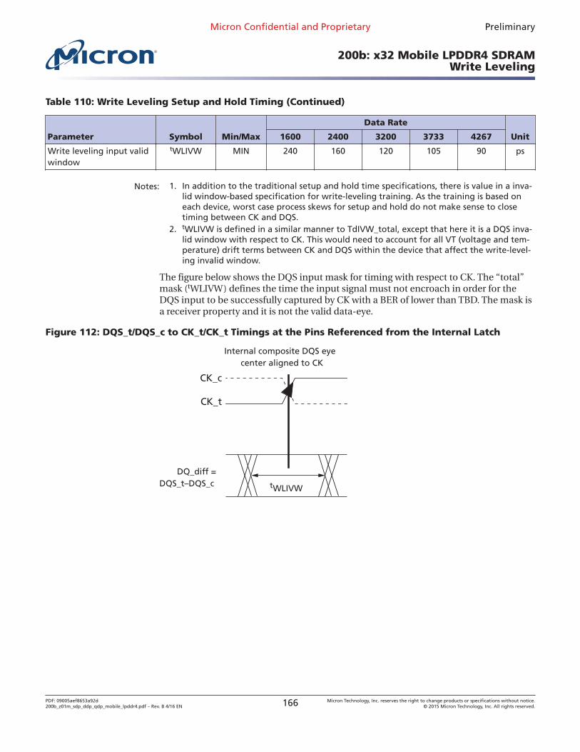
Table 110: Write Leveling Setup and Hold Timing (Continued)
Parameter Symbol Min/Max
Data Rate
Unit1600 2400 3200 3733 4267
Write leveling input validwindow
tWLIVW MIN 240 160 120 105 90 ps
Notes: 1. In addition to the traditional setup and hold time specifications, there is value in a inva-lid window-based specification for write-leveling training. As the training is based oneach device, worst case process skews for setup and hold do not make sense to closetiming between CK and DQS.
2. tWLIVW is defined in a similar manner to TdIVW_total, except that here it is a DQS inva-lid window with respect to CK. This would need to account for all VT (voltage and tem-perature) drift terms between CK and DQS within the device that affect the write-level-ing invalid window.
The figure below shows the DQS input mask for timing with respect to CK. The “total”mask (tWLIVW) defines the time the input signal must not encroach in order for theDQS input to be successfully captured by CK with a BER of lower than TBD. The mask isa receiver property and it is not the valid data-eye.
Figure 112: DQS_t/DQS_c to CK_t/CK_t Timings at the Pins Referenced from the Internal Latch
Internal composite DQS eyecenter aligned to CK
CK_t
CK_c
DQ_diff =DQS_t–DQS_c tWLIVW
Micron Confidential and Proprietary Preliminary
200b: x32 Mobile LPDDR4 SDRAMWrite Leveling
PDF: 09005aef8653a92d200b_z01m_sdp_ddp_qdp_mobile_lpddr4.pdf – Rev. B 4/16 EN 166 Micron Technology, Inc. reserves the right to change products or specifications without notice.
© 2015 Micron Technology, Inc. All rights reserved.
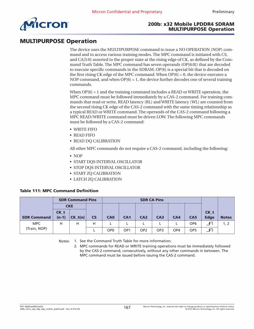
MULTIPURPOSE OperationThe device uses the MULTIPURPOSE command to issue a NO OPERATION (NOP) com-mand and to access various training modes. The MPC command is initiated with CS,and CA[5:0] asserted to the proper state at the rising edge of CK, as defined by the Com-mand Truth Table. The MPC command has seven operands (OP[6:0]) that are decodedto execute specific commands in the SDRAM. OP[6] is a special bit that is decoded onthe first rising CK edge of the MPC command. When OP[6] = 0, the device executes aNOP command, and when OP[6] = 1, the device further decodes one of several trainingcommands.
When OP[6] = 1 and the training command includes a READ or WRITE operation, theMPC command must be followed immediately by a CAS-2 command. For training com-mands that read or write, READ latency (RL) and WRITE latency (WL) are counted fromthe second rising CK edge of the CAS-2 command with the same timing relationship asa typical READ or WRITE command. The operands of the CAS-2 command following aMPC READ/WRITE command must be driven LOW. The following MPC commandsmust be followed by a CAS-2 command:
• WRITE FIFO• READ FIFO• READ DQ CALIBRATION
All other MPC commands do not require a CAS-2 command, including the following:
• NOP• START DQS INTERVAL OSCILLATOR• STOP DQS INTERVAL OSCILLATOR• START ZQ CALIBRATION• LATCH ZQ CALIBRATION
Table 111: MPC Command Definition
SDR Command
SDR Command Pins SDR CA Pins
CK_tEdge Notes
CKE
CS CA0 CA1 CA2 CA3 CA4 CA5CK_t (n-1) CK_t(n)
MPC(Train, NOP)
H H H L L L L L OP6 1 1, 2
L OP0 OP1 OP2 OP3 OP4 OP5 2
Notes: 1. See the Command Truth Table for more information.2. MPC commands for READ or WRITE training operations must be immediately followed
by the CAS-2 command, consecutively, without any other commands in between. TheMPC command must be issued before issuing the CAS-2 command.
Micron Confidential and Proprietary Preliminary
200b: x32 Mobile LPDDR4 SDRAMMULTIPURPOSE Operation
PDF: 09005aef8653a92d200b_z01m_sdp_ddp_qdp_mobile_lpddr4.pdf – Rev. B 4/16 EN 167 Micron Technology, Inc. reserves the right to change products or specifications without notice.
© 2015 Micron Technology, Inc. All rights reserved.
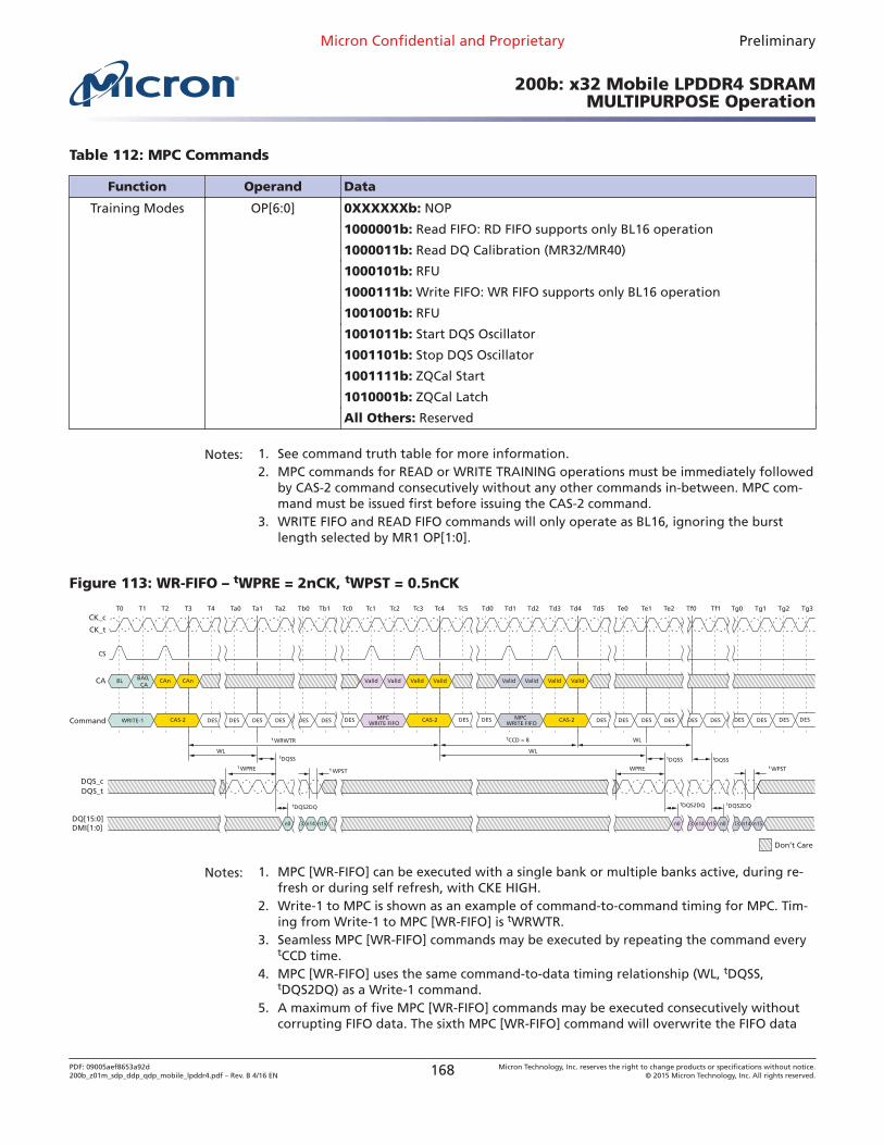
Table 112: MPC Commands
Function Operand Data
Training Modes OP[6:0] 0XXXXXXb: NOP
1000001b: Read FIFO: RD FIFO supports only BL16 operation
1000011b: Read DQ Calibration (MR32/MR40)
1000101b: RFU
1000111b: Write FIFO: WR FIFO supports only BL16 operation
1001001b: RFU
1001011b: Start DQS Oscillator
1001101b: Stop DQS Oscillator
1001111b: ZQCal Start
1010001b: ZQCal Latch
All Others: Reserved
Notes: 1. See command truth table for more information.2. MPC commands for READ or WRITE TRAINING operations must be immediately followed
by CAS-2 command consecutively without any other commands in-between. MPC com-mand must be issued first before issuing the CAS-2 command.
3. WRITE FIFO and READ FIFO commands will only operate as BL16, ignoring the burstlength selected by MR1 OP[1:0].
Figure 113: WR-FIFO – tWPRE = 2nCK, tWPST = 0.5nCK
T0 T1 T2 T3 Ta0 Ta2T4 Ta1 Tb0 Tb1 Tc0CK_c
CK_t
Tc4 Tc5Tc1 Tc2 Tc3 Td1 Td3Td0 Td2 Td5Td4 Te1 Tf1 Tg0 Tg1 Tg2 Tg3Te0 Te2 Tf0
CA
Command
CAn
DES DES
CAnBA0, CA
BL ValidValid Valid Valid ValidValid Valid Valid
t WRWTR
CAS-2 MPCWRITE FIFO
MPCWRITE FIFOWRITE-1 CAS-2 CAS-2
DQS_tDQS_c
DQ[15:0]DMI[1:0]
Don’t Care
tDQS2DQtDQS2DQ
tDQSSt WPRE t WPST
t WPST
n0 n13 n14 n15 n13 n14 n15n0 n13 n14 n15
WL
WL
WL
tCCD = 8
DES DES DES DES DES DESDES DES DES DES DES DES DES DES DES DES DES
CS
tDQSS
WPRE
tDQS2DQ
tDQSS
n0
Notes: 1. MPC [WR-FIFO] can be executed with a single bank or multiple banks active, during re-fresh or during self refresh, with CKE HIGH.
2. Write-1 to MPC is shown as an example of command-to-command timing for MPC. Tim-ing from Write-1 to MPC [WR-FIFO] is tWRWTR.
3. Seamless MPC [WR-FIFO] commands may be executed by repeating the command everytCCD time.
4. MPC [WR-FIFO] uses the same command-to-data timing relationship (WL, tDQSS,tDQS2DQ) as a Write-1 command.
5. A maximum of five MPC [WR-FIFO] commands may be executed consecutively withoutcorrupting FIFO data. The sixth MPC [WR-FIFO] command will overwrite the FIFO data
Micron Confidential and Proprietary Preliminary
200b: x32 Mobile LPDDR4 SDRAMMULTIPURPOSE Operation
PDF: 09005aef8653a92d200b_z01m_sdp_ddp_qdp_mobile_lpddr4.pdf – Rev. B 4/16 EN 168 Micron Technology, Inc. reserves the right to change products or specifications without notice.
© 2015 Micron Technology, Inc. All rights reserved.
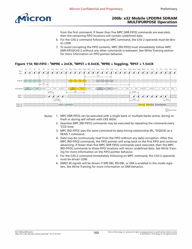
from the first command. If fewer than five MPC [WR-FIFO] commands are executed,then the remaining FIFO locations will contain undefined data.
6. For the CAS-2 command following an MPC command, the CAS-2 operands must be driv-en LOW.
7. To avoid corrupting the FIFO contents, MPC [RD-FIFO] must immediately follow MPC[WR-FIFO]/CAS-2 without any other commands in-between. See Write Training sectionfor more information on FIFO pointer behavior.
Figure 114: RD-FIFO – tWPRE = 2nCK, tWPST = 0.5nCK, tRPRE = Toggling, tRPST = 1.5nCK
T0 T1 T2 T3 Ta Ta+2T4 Ta+1 Ta+3 Tb Tb+2Tb+1 Tb+3 Tb+4 Tc+2Tb+5CK_c
CK_t
Tc+4 Tc+5 Tc+6 Tc+7Tc+3 Td+1 Td+3Td Td+2 Td+5Td+4
CA[5:0]
Command
DQS_cDQS_t
DQ[15:0]DMI[1:0]
Valid Valid
Valid ValidValidValidValid Valid
Valid
Valid Valid
Valid
Valid Valid ValidValid Valid Valid Valid Valid ValidValid Valid Valid Valid Valid Valid Valid Valid Valid Valid ValidValid
ValidValid Valid Valid Valid
Valid Valid Valid
Valid
Valid Valid
Valid
Don’t Care
tDQSS
tDQS2DQ
tDQSCK
tRPRE tRPST
CAS-2 MPCREAD FIFO
MPCWRITE FIFO
CAS-2 MPCREAD FIFO
CAS-2
Te+1 Tf+1Te Tf Tf+3Tf+2 Tf+4
D0 D1 D2 D13 D14 D15 D0 D11 D12 D13 D14 D15D0 D1 D12 D13 D14 D15
tCCD
RLWL
tWTR
Notes: 1. MPC [WR-FIFO] can be executed with a single bank or multiple banks active, during re-fresh or during self refresh with CKE HIGH.
2. Seamless MPC [RD-FIFO] commands may be executed by repeating the command everytCCD time.
3. MPC [RD-FIFO] uses the same command-to-data timing relationship (RL, tDQSCK) as aREAD-1 command.
4. Data may be continuously read from the FIFO without any data corruption. After fiveMPC [RD-FIFO] commands, the FIFO pointer will wrap back to the first FIFO and continueadvancing. If fewer than five MPC [WR-FIFO] commands were executed, then the MPC[RD-FIFO] commands to those FIFO locations will return undefined data. See Write Train-ing for more information on the FIFO pointer behavior.
5. For the CAS-2 command immediately following an MPC command, the CAS-2 operandsmust be driven LOW.
6. DMI[1:0] signals will be driven if WR-DBI, RD-DBI, or DM is enabled in the mode regis-ters. See Write Training for more information on DMI behavior.
Micron Confidential and Proprietary Preliminary
200b: x32 Mobile LPDDR4 SDRAMMULTIPURPOSE Operation
PDF: 09005aef8653a92d200b_z01m_sdp_ddp_qdp_mobile_lpddr4.pdf – Rev. B 4/16 EN 169 Micron Technology, Inc. reserves the right to change products or specifications without notice.
© 2015 Micron Technology, Inc. All rights reserved.
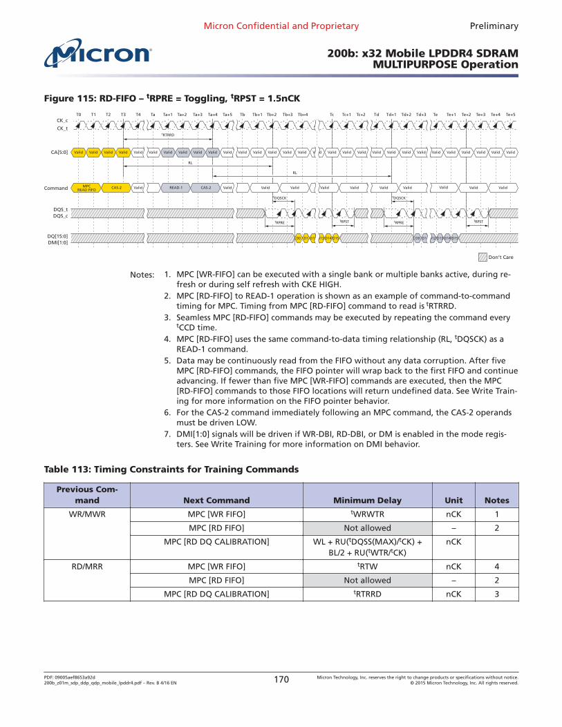
Figure 115: RD-FIFO – tRPRE = Toggling, tRPST = 1.5nCK
T0 T1 T2 T3 Ta Ta+2T4 Ta+1 Ta+3 Ta+4 Tb Tb+2Ta+5 Tb+1 Tb+3 Tb+4 Tc Tc+2Tc+1CK_c
CK_t
Td+1 TeTd Td+2 Td+3 Te+2 Te+3 Te+4 Te+5Te+1
CA[5:0]
Command
RL
RL
DQS_cDQS_t
DQ[15:0]DMI[1:0]
Valid Valid
Valid ValidValidValidValid Valid ValidValid Valid Valid Valid Valid ValidValid Valid Valid Valid Valid Valid Valid Valid Valid Valid ValidValid
ValidValid Valid Valid Valid
Valid Valid Valid Valid Valid
Valid Valid
Don’t Care
tDQSCK
tRPRE
tDQSCK
tRPRE
CAS-2 READ-1MPCREAD FIFO
CAS-2
D0 D1 D12 D13 D14 D15 D0 D1 D12 D13 D14 D15
tRTRRD
ValidValid
tRPSTtRPST
Notes: 1. MPC [WR-FIFO] can be executed with a single bank or multiple banks active, during re-fresh or during self refresh with CKE HIGH.
2. MPC [RD-FIFO] to READ-1 operation is shown as an example of command-to-commandtiming for MPC. Timing from MPC [RD-FIFO] command to read is tRTRRD.
3. Seamless MPC [RD-FIFO] commands may be executed by repeating the command everytCCD time.
4. MPC [RD-FIFO] uses the same command-to-data timing relationship (RL, tDQSCK) as aREAD-1 command.
5. Data may be continuously read from the FIFO without any data corruption. After fiveMPC [RD-FIFO] commands, the FIFO pointer will wrap back to the first FIFO and continueadvancing. If fewer than five MPC [WR-FIFO] commands are executed, then the MPC[RD-FIFO] commands to those FIFO locations will return undefined data. See Write Train-ing for more information on the FIFO pointer behavior.
6. For the CAS-2 command immediately following an MPC command, the CAS-2 operandsmust be driven LOW.
7. DMI[1:0] signals will be driven if WR-DBI, RD-DBI, or DM is enabled in the mode regis-ters. See Write Training for more information on DMI behavior.
Table 113: Timing Constraints for Training Commands
Previous Com-mand Next Command Minimum Delay Unit Notes
WR/MWR MPC [WR FIFO] tWRWTR nCK 1
MPC [RD FIFO] Not allowed – 2
MPC [RD DQ CALIBRATION] WL + RU(tDQSS(MAX)/tCK) +BL/2 + RU(tWTR/tCK)
nCK
RD/MRR MPC [WR FIFO] tRTW nCK 4
MPC [RD FIFO] Not allowed – 2
MPC [RD DQ CALIBRATION] tRTRRD nCK 3
Micron Confidential and Proprietary Preliminary
200b: x32 Mobile LPDDR4 SDRAMMULTIPURPOSE Operation
PDF: 09005aef8653a92d200b_z01m_sdp_ddp_qdp_mobile_lpddr4.pdf – Rev. B 4/16 EN 170 Micron Technology, Inc. reserves the right to change products or specifications without notice.
© 2015 Micron Technology, Inc. All rights reserved.
Table 113: Timing Constraints for Training Commands (Continued)
Previous Com-mand Next Command Minimum Delay Unit Notes
MPC [WR FIFO] WR/MWR Not allowed – 2
MPC [WR FIFO] tCCD nCK
RD/MRR Not allowed – 2
MPC [RD FIFO] WL + RU(tDQSS(MAX)/tCK) +BL/2 + RU(tWTR/tCK)
nCK
MPC [RD DQ CALIBRATION] Not allowed – 2
MPC [RD FIFO] WR/MWR tRTW nCK 4
MPC [WR FIFO] tRTW nCK 4
RD/MRR tRTRRD nCK 3
MPC [RD FIFO] tCCD nCK
MPC [RD DQ CALIBRATION] tRTRRD nCK 3
MPC [RD DQ CALI-BRATION]
WR/MWR tRTW nCK 4
MPC [WR FIFO] tRTW nCK 4
RD/MRR tRTRRD nCK 3
MPC [RD FIFO] Not allowed – 2
MPC [RD DQ CALIBRATION] tCCD nCK
Notes: 1. tWRWTR = WL + BL/2 + RU(tDQSS (MAX)/tCK) + MAX(RU(7.5ns/tCK), 8nCK).2. No commands are allowed between MPC [WR FIFO] and MPC [RD FIFO] except the MRW
commands related to training parameters.3. t RTRRD = RL + RU(tDQSCK (MAX)/tCK) + BL/2 + t RPST + 0.5 + MAX(RU(7.5ns/tCK), 8nCK).4. In case of DQ ODT disable MR11 OP[2:0] = 000b,
tRTW = RL + RU(tDQSCK (MAX)/tCK) + BL/2 - WL + tWPRE + RD(tRPST).
In case of DQ ODT enable MR11 OP[2:0] ≠ 000b,
tRTW = RL + RU(tDQSCK (MAX)/tCK) + BL/2 + tRPST - ODTLon - RD(tODTon(Min)/tCK) + 1.
Micron Confidential and Proprietary Preliminary
200b: x32 Mobile LPDDR4 SDRAMMULTIPURPOSE Operation
PDF: 09005aef8653a92d200b_z01m_sdp_ddp_qdp_mobile_lpddr4.pdf – Rev. B 4/16 EN 171 Micron Technology, Inc. reserves the right to change products or specifications without notice.
© 2015 Micron Technology, Inc. All rights reserved.
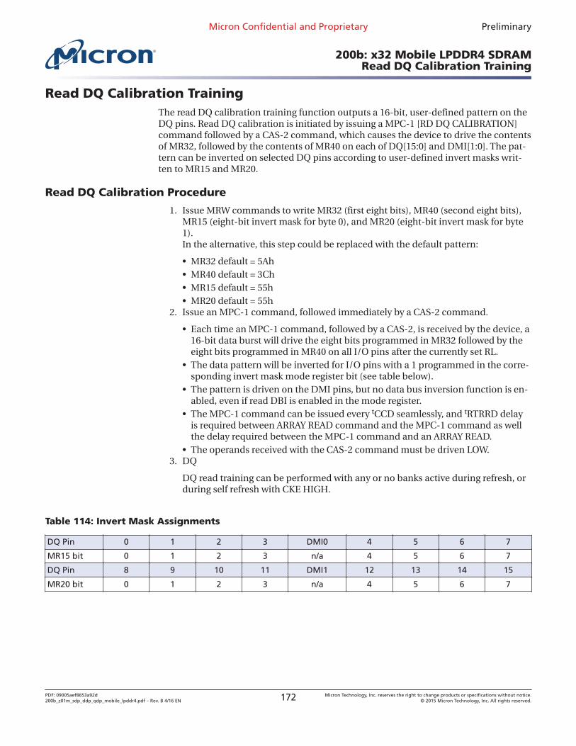
Read DQ Calibration TrainingThe read DQ calibration training function outputs a 16-bit, user-defined pattern on theDQ pins. Read DQ calibration is initiated by issuing a MPC-1 [RD DQ CALIBRATION]command followed by a CAS-2 command, which causes the device to drive the contentsof MR32, followed by the contents of MR40 on each of DQ[15:0] and DMI[1:0]. The pat-tern can be inverted on selected DQ pins according to user-defined invert masks writ-ten to MR15 and MR20.
Read DQ Calibration Procedure
1. Issue MRW commands to write MR32 (first eight bits), MR40 (second eight bits),MR15 (eight-bit invert mask for byte 0), and MR20 (eight-bit invert mask for byte1).In the alternative, this step could be replaced with the default pattern:
• MR32 default = 5Ah• MR40 default = 3Ch• MR15 default = 55h• MR20 default = 55h
2. Issue an MPC-1 command, followed immediately by a CAS-2 command.
• Each time an MPC-1 command, followed by a CAS-2, is received by the device, a16-bit data burst will drive the eight bits programmed in MR32 followed by theeight bits programmed in MR40 on all I/O pins after the currently set RL.
• The data pattern will be inverted for I/O pins with a 1 programmed in the corre-sponding invert mask mode register bit (see table below).
• The pattern is driven on the DMI pins, but no data bus inversion function is en-abled, even if read DBI is enabled in the mode register.
• The MPC-1 command can be issued every tCCD seamlessly, and tRTRRD delayis required between ARRAY READ command and the MPC-1 command as wellthe delay required between the MPC-1 command and an ARRAY READ.
• The operands received with the CAS-2 command must be driven LOW.3. DQ
DQ read training can be performed with any or no banks active during refresh, orduring self refresh with CKE HIGH.
Table 114: Invert Mask Assignments
DQ Pin 0 1 2 3 DMI0 4 5 6 7
MR15 bit 0 1 2 3 n/a 4 5 6 7
DQ Pin 8 9 10 11 DMI1 12 13 14 15
MR20 bit 0 1 2 3 n/a 4 5 6 7
Micron Confidential and Proprietary Preliminary
200b: x32 Mobile LPDDR4 SDRAMRead DQ Calibration Training
PDF: 09005aef8653a92d200b_z01m_sdp_ddp_qdp_mobile_lpddr4.pdf – Rev. B 4/16 EN 172 Micron Technology, Inc. reserves the right to change products or specifications without notice.
© 2015 Micron Technology, Inc. All rights reserved.
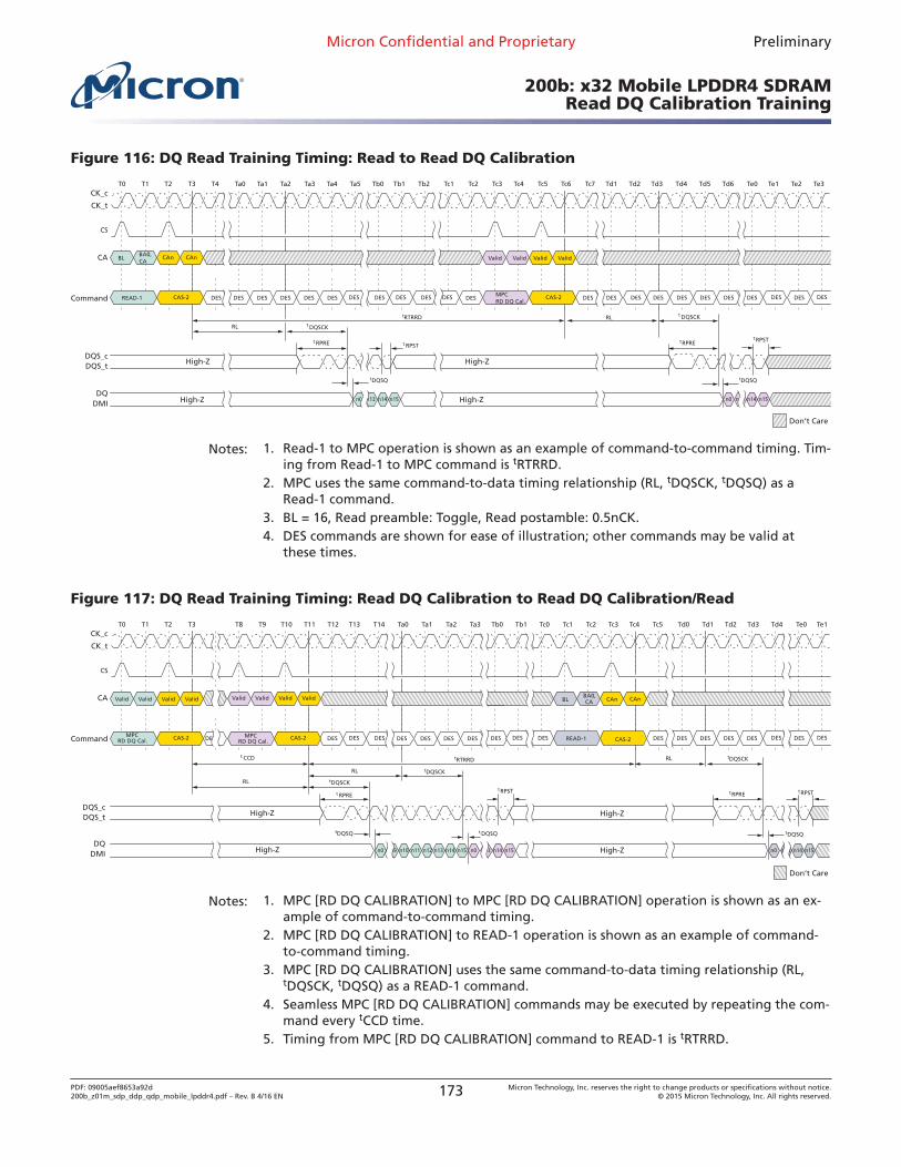
Figure 116: DQ Read Training Timing: Read to Read DQ Calibration
T0 T1 T2 T3 Ta0 Ta2T4 Ta1 Ta3 Ta5Ta4 Tb0 Tb1 Tb2CK_c
CK_t
Tc4 Tc5 Tc6 Tc7Tc1 Tc2 Tc3 Td1 Td3Td2 Td5Td4 Te1Te0Td6 Te2 Te3
CA
Command
CAn
DES DES
CAnBLBA0,CA ValidValid ValidValid
CAS-2 MPCRD DQ Cal.
READ-1 CAS-2
DQS_tDQS_c
DQDMI
Don’t Care
tDQSQ t
t
DQSQ
t DQSCK
t RPRE t RPSTtRPST
n0 n13 n14 n15n0 n13 n14 n15
RLtRTRRD
DES DES DES DES DES DES DES DES DES DES DES DES DESDES DES DES DES DES DES DES
CS
RPRE
t DQSCK
DES
RL
High-Z
High-Z
High-Z
High-Z
Notes: 1. Read-1 to MPC operation is shown as an example of command-to-command timing. Tim-ing from Read-1 to MPC command is tRTRRD.
2. MPC uses the same command-to-data timing relationship (RL, tDQSCK, tDQSQ) as aRead-1 command.
3. BL = 16, Read preamble: Toggle, Read postamble: 0.5nCK.4. DES commands are shown for ease of illustration; other commands may be valid at
these times.
Figure 117: DQ Read Training Timing: Read DQ Calibration to Read DQ Calibration/Read
T0 T1 T2 T3 T9 T11T8 T10 T12 T13 T14 Ta0CK_c
CK_t
Tb0 Tb1Ta1 Ta2 Ta3 Tc1 Tc3Tc0 Tc2 Tc5Tc4 Td1 Te0 Te1Td0 Td2 Td3 Td4
CA
Command DES
ValidValid Valid ValidValidValid Valid Valid BA0,BL CA CAn CAn
CAS-2 MPCMPCRD DQ Cal. RD DQ Cal. READ-1CAS-2 CAS-2
DQS_tDQS_c
Don’t Care
tDQSQ t
t
DQSQ
tDQSCK
tDQSCK
tDQSCK
t CCD
t RPREtRPST
tRPST
n0 n9 n10 n11
RL
RL
RL
tRTRRD
DES DES DES DESDES DES DES DES DES DES DES DES DES DES DES DES DES DES
CS
tDQSQ
RPRE
n13 n14 n15n0n12 n13 n14 n15 n13 n14 n15n0
High-Z
High-Z
High-Z
High-ZDQ
DMI
Notes: 1. MPC [RD DQ CALIBRATION] to MPC [RD DQ CALIBRATION] operation is shown as an ex-ample of command-to-command timing.
2. MPC [RD DQ CALIBRATION] to READ-1 operation is shown as an example of command-to-command timing.
3. MPC [RD DQ CALIBRATION] uses the same command-to-data timing relationship (RL,tDQSCK, tDQSQ) as a READ-1 command.
4. Seamless MPC [RD DQ CALIBRATION] commands may be executed by repeating the com-mand every tCCD time.
5. Timing from MPC [RD DQ CALIBRATION] command to READ-1 is tRTRRD.
Micron Confidential and Proprietary Preliminary
200b: x32 Mobile LPDDR4 SDRAMRead DQ Calibration Training
PDF: 09005aef8653a92d200b_z01m_sdp_ddp_qdp_mobile_lpddr4.pdf – Rev. B 4/16 EN 173 Micron Technology, Inc. reserves the right to change products or specifications without notice.
© 2015 Micron Technology, Inc. All rights reserved.
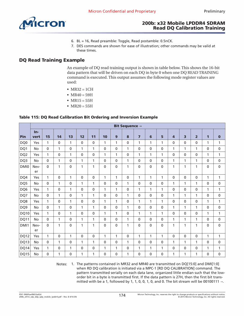
6. BL = 16, Read preamble: Toggle, Read postamble: 0.5nCK.7. DES commands are shown for ease of illustration; other commands may be valid at
these times.
DQ Read Training Example
An example of DQ read training output is shown in table below. This shows the 16-bitdata pattern that will be driven on each DQ in byte 0 when one DQ READ TRAININGcommand is executed. This output assumes the following mode register values areused:
• MR32 = 1CH• MR40 = 59H• MR15 = 55H• MR20 = 55H
Table 115: DQ Read Calibration Bit Ordering and Inversion Example
Pin
Bit Sequence →→In-
vert 15 14 13 12 11 10 9 8 7 6 5 4 3 2 1 0
DQ0 Yes 1 0 1 0 0 1 1 0 1 1 1 0 0 0 1 1
DQ1 No 0 1 0 1 1 0 0 1 0 0 0 1 1 1 0 0
DQ2 Yes 1 0 1 0 0 1 1 0 1 1 1 0 0 0 1 1
DQ3 No 0 1 0 1 1 0 0 1 0 0 0 1 1 1 0 0
DMI0 Nev-er
0 1 0 1 1 0 0 1 0 0 0 1 1 1 0 0
DQ4 Yes 1 0 1 0 0 1 1 0 1 1 1 0 0 0 1 1
DQ5 No 0 1 0 1 1 0 0 1 0 0 0 1 1 1 0 0
DQ6 Yes 1 0 1 0 0 1 1 0 1 1 1 0 0 0 1 1
DQ7 No 0 1 0 1 1 0 0 1 0 0 0 1 1 1 0 0
DQ8 Yes 1 0 1 0 0 1 1 0 1 1 1 0 0 0 1 1
DQ9 No 0 1 0 1 1 0 0 1 0 0 0 1 1 1 0 0
DQ10 Yes 1 0 1 0 0 1 1 0 1 1 1 0 0 0 1 1
DQ11 No 0 1 0 1 1 0 0 1 0 0 0 1 1 1 0 0
DMI1 Nev-er
0 1 0 1 1 0 0 1 0 0 0 1 1 1 0 0
DQ12 Yes 1 0 1 0 0 1 1 0 1 1 1 0 0 0 1 1
DQ13 No 0 1 0 1 1 0 0 1 0 0 0 1 1 1 0 0
DQ14 Yes 1 0 1 0 0 1 1 0 1 1 1 0 0 0 1 1
DQ15 No 0 1 0 1 1 0 0 1 0 0 0 1 1 1 0 0
Notes: 1. The patterns contained in MR32 and MR40 are transmitted on DQ[15:0] and DMI[1:0]when RD DQ calibration is initiated via a MPC-1 [RD DQ CALIBRATION] command. Thepattern transmitted serially on each data lane, organized little endian such that the low-order bit in a byte is transmitted first. If the data pattern is 27H, then the first bit trans-mitted with be a 1, followed by 1, 1, 0, 0, 1, 0, and 0. The bit stream will be 00100111 →.
Micron Confidential and Proprietary Preliminary
200b: x32 Mobile LPDDR4 SDRAMRead DQ Calibration Training
PDF: 09005aef8653a92d200b_z01m_sdp_ddp_qdp_mobile_lpddr4.pdf – Rev. B 4/16 EN 174 Micron Technology, Inc. reserves the right to change products or specifications without notice.
© 2015 Micron Technology, Inc. All rights reserved.
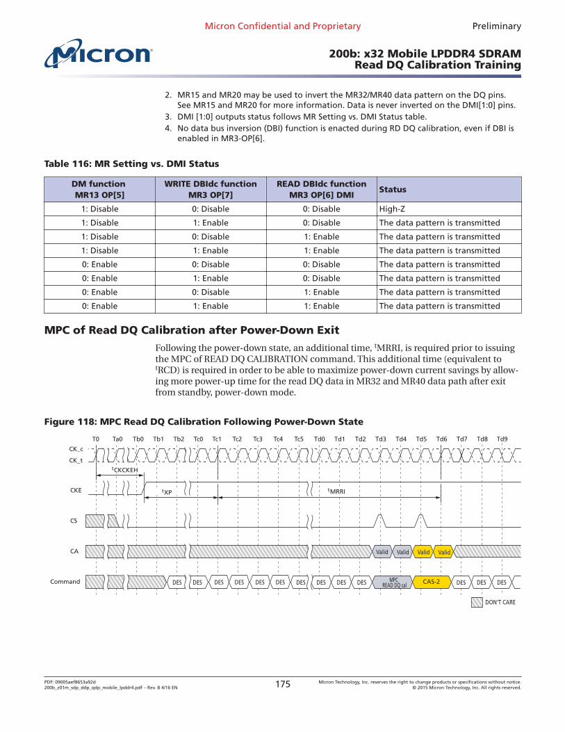
2. MR15 and MR20 may be used to invert the MR32/MR40 data pattern on the DQ pins.See MR15 and MR20 for more information. Data is never inverted on the DMI[1:0] pins.
3. DMI [1:0] outputs status follows MR Setting vs. DMI Status table.4. No data bus inversion (DBI) function is enacted during RD DQ calibration, even if DBI is
enabled in MR3-OP[6].
Table 116: MR Setting vs. DMI Status
DM function MR13 OP[5]
WRITE DBIdc functionMR3 OP[7]
READ DBIdc functionMR3 OP[6] DMI
Status
1: Disable 0: Disable 0: Disable High-Z
1: Disable 1: Enable 0: Disable The data pattern is transmitted
1: Disable 0: Disable 1: Enable The data pattern is transmitted
1: Disable 1: Enable 1: Enable The data pattern is transmitted
0: Enable 0: Disable 0: Disable The data pattern is transmitted
0: Enable 1: Enable 0: Disable The data pattern is transmitted
0: Enable 0: Disable 1: Enable The data pattern is transmitted
0: Enable 1: Enable 1: Enable The data pattern is transmitted
MPC of Read DQ Calibration after Power-Down Exit
Following the power-down state, an additional time, tMRRI, is required prior to issuingthe MPC of READ DQ CALIBRATION command. This additional time (equivalent totRCD) is required in order to be able to maximize power-down current savings by allow-ing more power-up time for the read DQ data in MR32 and MR40 data path after exitfrom standby, power-down mode.
Figure 118: MPC Read DQ Calibration Following Power-Down State
T0
CK_t
CK_c
Ta0 Tb0 Tb1
CA
Tb2 Tc1
Command
CS
CKE
Td1
DON'T CARE
Tc0 Td7Td2Tc5 Td3 Td6Td4Tc2 Tc3 Tc4 Td0 Td5 Td8 Td9
DES DES DES DESDES DES DES DES
Valid
DES DES DES DESMPCREAD DQ cal CAS-2DES
tCKCKEH
tMRRItXP
Valid Valid Valid
Micron Confidential and Proprietary Preliminary
200b: x32 Mobile LPDDR4 SDRAMRead DQ Calibration Training
PDF: 09005aef8653a92d200b_z01m_sdp_ddp_qdp_mobile_lpddr4.pdf – Rev. B 4/16 EN 175 Micron Technology, Inc. reserves the right to change products or specifications without notice.
© 2015 Micron Technology, Inc. All rights reserved.
Write TrainingThe device uses an unmatched DQS-DQ path to enable high-speed performance andsave power. As a result, the DQS strobe must be trained to arrive at the DQ latch center-aligned with the data eye. The DQ receiver is located at the DQ pad and has a shorterinternal delay than the DQS signal. The DQ receiver will latch the data present on theDQ bus when DQS reaches the latch, and write training is accomplished by delaying theDQ signals relative to DQS such that the data eye arrives at the receiver latch centeredon the DQS transition.
Two modes of training are available:
• Command-based FIFO WR/RD with user patterns• An internal DQS clock-tree oscillator, which determines the need for, and the magni-
tude of, required training
The command-based FIFO WR/RD uses the MPC command with operands to enablethis special mode of operation. When issuing the MPC command, if CA[5] is set LOW(OP[6] = 0), then the device will perform a NOP command. When CA[5] is set HIGH, theCA[4:0] pins enable training functions or are reserved for future use (RFU). MPC com-mands that initiate a read or write to the device must be followed immediately by aCAS-2 command. See the MPC Operation section for more information.
To perform write training, the controller can issue an MPC [WRITE DQ FIFO] commandwith OP[6:0] set, followed immediately by a CAS-2 command (CAS-2 operands shouldbe driven LOW) to initiate a WRITE DQ FIFO. Timings for MPC [WRITE DQ FIFO] areidentical to WRITE commands, with WL timed from the second rising clock edge of theCAS-2 command. Up to five consecutive MPC [WRITE DQ FIFO] commands with user-defined patterns may be issued to the device, which will store up to 80 values (BL16 × 5)per pin that can be read back via the MPC [READ DQ FIFO] command. (The WRITE/READ FIFO POINTER operation is described in a different section.
After writing data with the MPC [WRITE DQ FIFO] command, the data can be read backwith the MPC [READ DQ FIFO] command and results can be compared with "expected"data to determine whether further training (DQ delay) is needed. MPC [READ DQ FIFO]is initiated by issuing an MPC command, as described in the MPC Operation section,followed immediately by a CAS-2 command (CAS-2 operands must be driven LOW).Timings for the MPC [READ DQ FIFO] command are identical to READ commands,with RL timed from the second rising clock edge of the CAS-2 command.
READ DQ FIFO is nondestructive to the data captured in the FIFO; data may be readcontinuously until it is disturbed by another command, such as a READ, WRITE, or an-other MPC [WRITE DQ FIFO]. If fewer than five WRITE DQ FIFO commands are execu-ted, unwritten registers will have undefined (but valid) data when read back.
For example: If five WRITE DQ FIFO commands are executed sequentially, then a seriesof READ DQ FIFO commands will read valid data from FIFO[0], FIFO[1]….FIFO[4] andthen wrap back to FIFO[0] on the next READ DQ FIFO. However, if fewer than fiveWRITE DQ FIFO commands are executed sequentially (example = 3), then a series ofREAD DQ FIFO commands will return valid data for FIFO[0], FIFO[1], and FIFO[2], butthe next two READ DQ FIFO commands will return undefined data for FIFO[3] andFIFO[4] before wrapping back to the valid data in FIFO[0].
The READ DQ FIFO pointer and WRITE DQ FIFO pointer are reset under the followingconditions:
Micron Confidential and Proprietary Preliminary
200b: x32 Mobile LPDDR4 SDRAMWrite Training
PDF: 09005aef8653a92d200b_z01m_sdp_ddp_qdp_mobile_lpddr4.pdf – Rev. B 4/16 EN 176 Micron Technology, Inc. reserves the right to change products or specifications without notice.
© 2015 Micron Technology, Inc. All rights reserved.
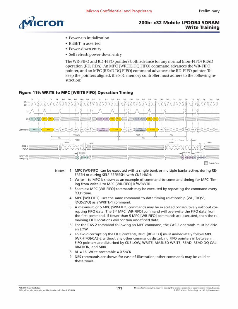
• Power-up initialization• RESET_n asserted• Power-down entry• Self refresh power-down entry
The WR-FIFO and RD-FIFO pointers both advance for any normal (non-FIFO) READoperation (RD, RDA). An MPC [WRITE DQ FIFO] command advances the WR-FIFOpointer, and an MPC [READ DQ FIFO] command advances the RD-FIFO pointer. Tokeep the pointers aligned, the SoC memory controller must adhere to the following re-striction:
Figure 119: WRITE to MPC [WRITE FIFO] Operation Timing
T0 T1 T2 T3 Ta0 Ta2T4 Ta1 Tb0 Tb1 Tc0CK_c
CK_t
Tc4 Tc5Tc1 Tc2 Tc3 Td1 Td3Td0 Td2 Td5Td4 Te1 Tf1 Tg0 Tg1 Tg2 Tg3Te0 Te2 Tf0
CA
Command
CAn
DES DES
CAnBA0, CA
BL ValidValid Valid Valid ValidValid Valid Valid
t WRWTR
CAS-2 MPCWRITE FIFO
MPCWRITE FIFOWRITE-1 CAS-2 CAS-2
DQS_tDQS_c
DQ[15:0]DMI[1:0]
Don’t Care
tDQS2DQtDQS2DQ
tDQSSt WPRE t WPST
t WPST
n0 n13 n14 n15 n13 n14 n15n0 n13 n14 n15
WL
WL
WL
tCCD = 8
DES DES DES DES DES DESDES DES DES DES DES DES DES DES DES DES DES
CS
tDQSS
WPRE
tDQS2DQ
tDQSS
n0
Notes: 1. MPC [WR-FIFO] can be executed with a single bank or multiple banks active, during RE-FRESH or during SELF REFRESH, with CKE HIGH.
2. Write-1 to MPC is shown as an example of command-to-command timing for MPC. Tim-ing from write-1 to MPC [WR-FIFO] is tWRWTR.
3. Seamless MPC [WR-FIFO] commands may be executed by repeating the command everytCCD time.
4. MPC [WR-FIFO] uses the same command-to-data timing relationship (WL, tDQSS,tDQS2DQ) as a WRITE-1 command.
5. A maximum of 5 MPC [WR-FIFO] commands may be executed consecutively without cor-rupting FIFO data. The 6th MPC [WR-FIFO] command will overwrite the FIFO data fromthe first command. If fewer than 5 MPC [WR-FIFO] commands are executed, then the re-maining FIFO locations will contain undefined data.
6. For the CAS-2 command following an MPC command, the CAS-2 operands must be driv-en LOW.
7. To avoid corrupting the FIFO contents, MPC [RD-FIFO] must immediately follow MPC[WR-FIFO]/CAS-2 without any other commands disturbing FIFO pointers in between.FIFO pointers are disturbed by CKE LOW, WRITE, MASKED WRITE, READ, READ DQ CALI-BRATION, and MRR.
8. BL = 16, Write postamble = 0.5nCK9. DES commands are shown for ease of illustration; other commands may be valid at
these times.
Micron Confidential and Proprietary Preliminary
200b: x32 Mobile LPDDR4 SDRAMWrite Training
PDF: 09005aef8653a92d200b_z01m_sdp_ddp_qdp_mobile_lpddr4.pdf – Rev. B 4/16 EN 177 Micron Technology, Inc. reserves the right to change products or specifications without notice.
© 2015 Micron Technology, Inc. All rights reserved.
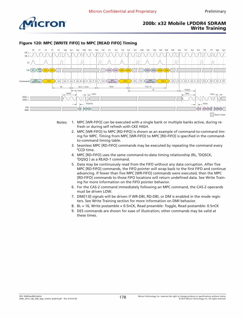
Figure 120: MPC [WRITE FIFO] to MPC [READ FIFO] Timing
T0 T1 T2 T3 Ta0 Ta2T4 Ta1 Tb0 Tb1 Tb2 Tc0CK_c
CK_t
Tc4 Tc5Tc1 Tc2 Tc3 Td1 Td3Td0 Td2 Td5Td4 Te1 Tf1 Tg0 Tg1Te0 Te2 Te3 Tf0
CA
Command
CAn
DES DES
CAnBA0, CA
BL ValidValid Valid Valid ValidValid Valid Valid
BL/2 + 1 clock
CAS-2 MPCREAD FIFO
MPCWRITE FIFO
MPCREAD FIFO
CAS-2 CAS-2
DQS_tDQS_c
DQDMI
Don’t Care
tDQS2DQ t
t
DQSQ
tDQSCKtDQSSt WPRE t WPST tRPST
n0 n13 n14 n15 n13 n14 n15n0 n13 n14 n15
RL
WL tCCD = 8tWTR
DES DES DES DES DES DESDES DES DES DES DES DES DES DES DES DES DES
CS
RPRE
n0
Notes: 1. MPC [WR-FIFO] can be executed with a single bank or multiple banks active, during re-fresh or during self refresh with CKE HIGH.
2. MPC [WR-FIFO] to MPC [RD-FIFO] is shown as an example of command-to-command tim-ing for MPC. Timing from MPC [WR-FIFO] to MPC [RD-FIFO] is specified in the command-to-command timing table.
3. Seamless MPC [RD-FIFO] commands may be executed by repeating the command everytCCD time.
4. MPC [RD-FIFO] uses the same command-to-data timing relationship (RL, tDQSCK,tDQSQ ) as a READ-1 command.
5. Data may be continuously read from the FIFO without any data corruption. After fiveMPC [RD-FIFO] commands, the FIFO pointer will wrap back to the first FIFO and continueadvancing. If fewer than five MPC [WR-FIFO] commands were executed, then the MPC[RD-FIFO] commands to those FIFO locations will return undefined data. See Write Train-ing for more information on the FIFO pointer behavior.
6. For the CAS-2 command immediately following an MPC command, the CAS-2 operandsmust be driven LOW.
7. DMI[1:0] signals will be driven if WR-DBI, RD-DBI, or DM is enabled in the mode regis-ters. See Write Training section for more information on DMI behavior.
8. BL = 16, Write postamble = 0.5nCK, Read preamble: Toggle, Read postamble: 0.5nCK9. DES commands are shown for ease of illustration; other commands may be valid at
these times.
Micron Confidential and Proprietary Preliminary
200b: x32 Mobile LPDDR4 SDRAMWrite Training
PDF: 09005aef8653a92d200b_z01m_sdp_ddp_qdp_mobile_lpddr4.pdf – Rev. B 4/16 EN 178 Micron Technology, Inc. reserves the right to change products or specifications without notice.
© 2015 Micron Technology, Inc. All rights reserved.
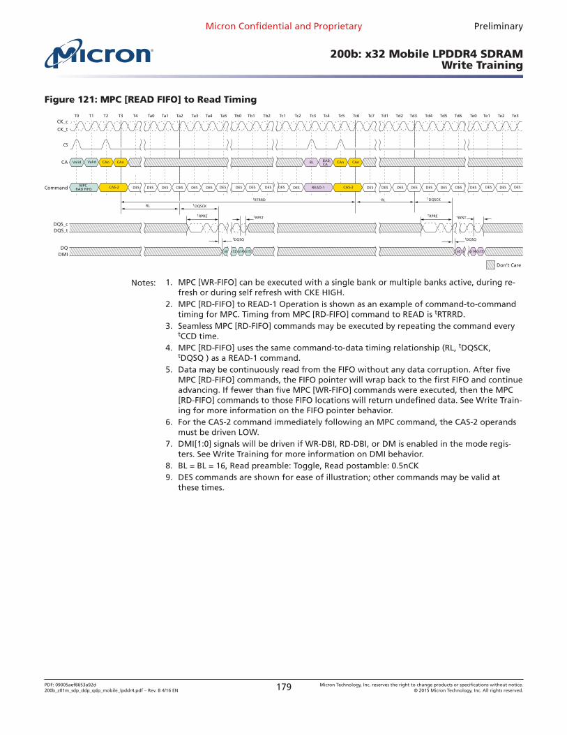
Figure 121: MPC [READ FIFO] to Read Timing
T0 T1 T2 T3 Ta0 Ta2T4 Ta1 Ta3 Ta5Ta4 Tb0 Tb1 Tb2CK_c
CK_t
Tc4 Tc5 Tc6 Tc7Tc1 Tc2 Tc3 Td1 Td3Td2 Td5Td4 Te1Te0Td6 Te2 Te3
CA
Command
CAn
DES DES
CAnValid Valid BA0,CA
BL CAn CAn
CAS-2 READ-1MPCRAD FIFO CAS-2
DQS_tDQS_c
Don’t Care
tDQSQ t
t
DQSQ
t DQSCK
t RPRE t RPST tRPST
n0 n13 n14 n15n0 n13 n14 n15
RLtRTRRD
DES DES DES DES DES DES DES DES DES DES DES DES DESDES DES DES DES DES DES DES
CS
RPRE
t DQSCK
DES
RL
DQDMI
Notes: 1. MPC [WR-FIFO] can be executed with a single bank or multiple banks active, during re-fresh or during self refresh with CKE HIGH.
2. MPC [RD-FIFO] to READ-1 Operation is shown as an example of command-to-commandtiming for MPC. Timing from MPC [RD-FIFO] command to READ is tRTRRD.
3. Seamless MPC [RD-FIFO] commands may be executed by repeating the command everytCCD time.
4. MPC [RD-FIFO] uses the same command-to-data timing relationship (RL, tDQSCK,tDQSQ ) as a READ-1 command.
5. Data may be continuously read from the FIFO without any data corruption. After fiveMPC [RD-FIFO] commands, the FIFO pointer will wrap back to the first FIFO and continueadvancing. If fewer than five MPC [WR-FIFO] commands were executed, then the MPC[RD-FIFO] commands to those FIFO locations will return undefined data. See Write Train-ing for more information on the FIFO pointer behavior.
6. For the CAS-2 command immediately following an MPC command, the CAS-2 operandsmust be driven LOW.
7. DMI[1:0] signals will be driven if WR-DBI, RD-DBI, or DM is enabled in the mode regis-ters. See Write Training for more information on DMI behavior.
8. BL = BL = 16, Read preamble: Toggle, Read postamble: 0.5nCK9. DES commands are shown for ease of illustration; other commands may be valid at
these times.
Micron Confidential and Proprietary Preliminary
200b: x32 Mobile LPDDR4 SDRAMWrite Training
PDF: 09005aef8653a92d200b_z01m_sdp_ddp_qdp_mobile_lpddr4.pdf – Rev. B 4/16 EN 179 Micron Technology, Inc. reserves the right to change products or specifications without notice.
© 2015 Micron Technology, Inc. All rights reserved.
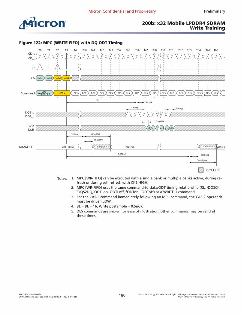
Figure 122: MPC [WRITE FIFO] with DQ ODT Timing
T0 T1 T2 T3 Ta0 Ta2T4 Ta1 Ta3 Ta5Ta4 Ta6 Ta8Ta7 Tb0 Tb1 Tb2 Tb3 Tb4 Tb5 Tb6CK_c
CK_t
CA
Command DES DES
Valid Valid Valid Valid
CAS-2MPCWRITE FIFO
DQS_tDQS_c
DRAM RTT
Don’t Care
tDQS2DQ
tDQSS
t
t
WPRE t WPST
n0 n1 n2 n13 n14 n15
WL
ODT High-Z ODT High-Z
DES DES DES DES DES DES DES DES DES DES DES DES DES
CS
ODTon(MAX)
tODTon(MIN)
tODToff(MAX)
tODToff(MIN)
Transition TransitionODT On
ODTLon
ODTLoff
DES DES
DQDMI
Notes: 1. MPC [WR-FIFO] can be executed with a single bank or multiple banks active, during re-fresh or during self refresh with CKE HIGH.
2. MPC [WR-FIFO] uses the same command-to-data/ODT timing relationship (RL, tDQSCK,tDQS2DQ, ODTLon, ODTLoff, tODTon, tODToff) as a WRITE-1 command.
3. For the CAS-2 command immediately following an MPC command, the CAS-2 operandsmust be driven LOW.
4. BL = BL = 16, Write postamble = 0.5nCK5. DES commands are shown for ease of illustration; other commands may be valid at
these times.
Micron Confidential and Proprietary Preliminary
200b: x32 Mobile LPDDR4 SDRAMWrite Training
PDF: 09005aef8653a92d200b_z01m_sdp_ddp_qdp_mobile_lpddr4.pdf – Rev. B 4/16 EN 180 Micron Technology, Inc. reserves the right to change products or specifications without notice.
© 2015 Micron Technology, Inc. All rights reserved.
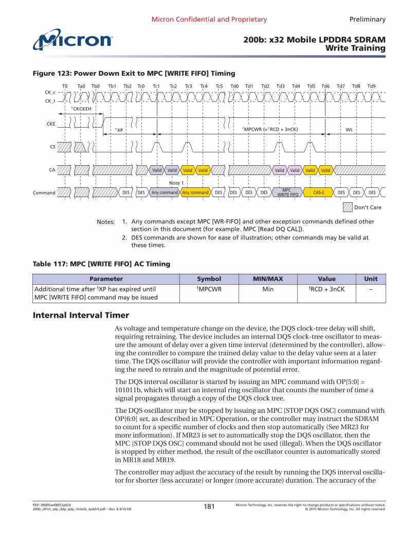
Figure 123: Power Down Exit to MPC [WRITE FIFO] Timing
T0
CK_t
CK_cTa0 Tc2 Tc3 Tc4
CA
Tc5Tc0 Tc1 Td2Td0 Td1 Td3 Td4 Td5 Td6 Td7 Td8 Td9Tb0 Tb1 Tb2
Command DESDES DESDES
Valid ValidValid Valid
DESAny command MPCWRITE FIFOAny command CAS-2
t XP
DESDES DES DES
CS
CKE
ValidValid ValidValid
Don’t Care
t tMPCWR (= RCD + 3nCK)
t CKCKEH
WL
Note 1
Notes: 1. Any commands except MPC [WR-FIFO] and other exception commands defined othersection in this document (for example. MPC [Read DQ CAL]).
2. DES commands are shown for ease of illustration; other commands may be valid atthese times.
Table 117: MPC [WRITE FIFO] AC Timing
Parameter Symbol MIN/MAX Value Unit
Additional time after tXP has expired untilMPC [WRITE FIFO] command may be issued
tMPCWR Min tRCD + 3nCK –
Internal Interval Timer
As voltage and temperature change on the device, the DQS clock-tree delay will shift,requiring retraining. The device includes an internal DQS clock-tree oscillator to meas-ure the amount of delay over a given time interval (determined by the controller), allow-ing the controller to compare the trained delay value to the delay value seen at a latertime. The DQS oscillator will provide the controller with important information regard-ing the need to retrain and the magnitude of potential error.
The DQS interval oscillator is started by issuing an MPC command with OP[5:0] =101011b, which will start an internal ring oscillator that counts the number of time asignal propagates through a copy of the DQS clock tree.
The DQS oscillator may be stopped by issuing an MPC [STOP DQS OSC] command withOP[6:0] set, as described in MPC Operation, or the controller may instruct the SDRAMto count for a specific number of clocks and then stop automatically (See MR23 formore information). If MR23 is set to automatically stop the DQS oscillator, then theMPC [STOP DQS OSC] command should not be used (illegal). When the DQS oscillatoris stopped by either method, the result of the oscillator counter is automatically storedin MR18 and MR19.
The controller may adjust the accuracy of the result by running the DQS interval oscilla-tor for shorter (less accurate) or longer (more accurate) duration. The accuracy of the
Micron Confidential and Proprietary Preliminary
200b: x32 Mobile LPDDR4 SDRAMWrite Training
PDF: 09005aef8653a92d200b_z01m_sdp_ddp_qdp_mobile_lpddr4.pdf – Rev. B 4/16 EN 181 Micron Technology, Inc. reserves the right to change products or specifications without notice.
© 2015 Micron Technology, Inc. All rights reserved.
result for a given temperature and voltage is determined by the following equation,where run time = total time between start and stop commands and DQS delay = the val-ue of the DQS clock tree delay (tDQS2DQ MIN/MAX):
DQS oscillator granularity error = 2 x (DQS delay)
run time
Additional matching error must be included, which is the difference between DQStraining circuit and the actual DQS clock tree across voltage and temperature. Thematching error is vendor specific. Therefore, the total accuracy of the DQS oscillatorcounter is given by:
DQS oscillator accuracy = 1 - granularity error - matching error
For example, if the total time between start and stop commands is 100ns, and the maxi-mum DQS clock tree delay is 800ps (tDQS2DQ MAX), then the DQS oscillator granulari-ty error is:
DQS oscillator granularity error = 2 x (0.8ns)
100ns= 1.6%
This equates to a granularity timing error of 12.8ps. Assuming a circuit matching errorof 5.5ps across voltage and temperature, the accuracy is:
DQS oscillator accuracy = 1 - 12.8 + 5.5
800= 97.7%
For example, running the DQS oscillator for a longer period improves the accuracy. Ifthe total time between start and stop commands is 500ns, and the maximum DQS clocktree delay is 800ps (tDQS2DQ MAX), then the DQS oscillator granularity error is:
DQS oscillator granularity error = 2 x (0.8ns)
500ns= 0.32%
This equates to a granularity timing error or 2.56ps. Assuming a circuit matching errorof 5.5ps across voltage and temperature, the accuracy is:
DQS oscillator accuracy = 1 - 2.56 + 5.5
800= 99.0%
The result of the DQS interval oscillator is defined as the number of DQS clock tree de-lays that can be counted within the run time, determined by the controller. The result isstored in MR18-OP[7:0] and MR19-OP[7:0].
MR18 contains the least significant bits (LSB) of the result, and MR19 contains the mostsignificant bits (MSB) of the result. MR18 and MR19 are overwritten by the SDRAMwhen a MPC [Stop DQS Osc] command is received.
The SDRAM counter will count to its maximum value (= 2^16) and stop. If the maxi-mum value is read from the mode registers, the memory controller must assume thatthe counter overflowed the register and therefore discard the result. The longest runtime for the oscillator that will not overflow the counter registers can be calculated asfollows:
Longest runtime interval = 216 x tDQS2DQ(MIN) = 216 × 0.2ns = 13.1μs
Micron Confidential and Proprietary Preliminary
200b: x32 Mobile LPDDR4 SDRAMWrite Training
PDF: 09005aef8653a92d200b_z01m_sdp_ddp_qdp_mobile_lpddr4.pdf – Rev. B 4/16 EN 182 Micron Technology, Inc. reserves the right to change products or specifications without notice.
© 2015 Micron Technology, Inc. All rights reserved.
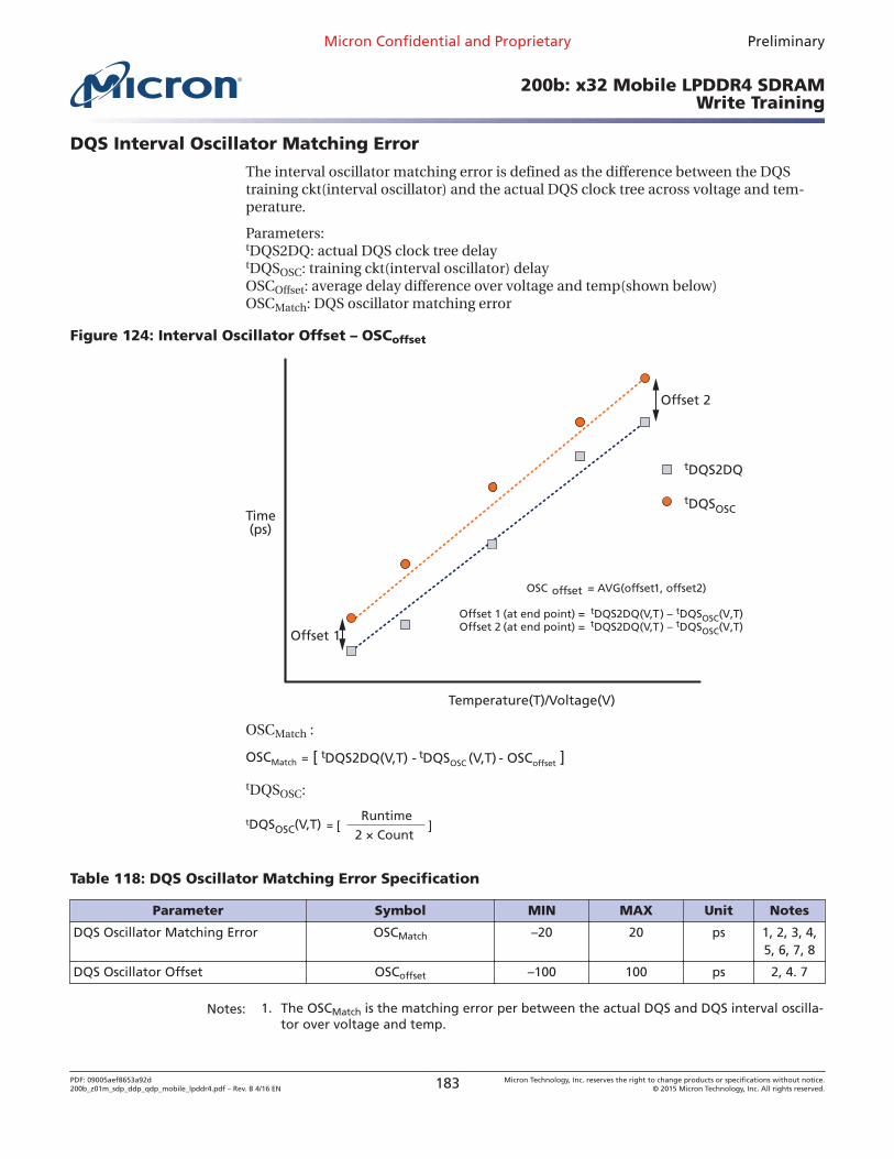
DQS Interval Oscillator Matching Error
The interval oscillator matching error is defined as the difference between the DQStraining ckt(interval oscillator) and the actual DQS clock tree across voltage and tem-perature.
Parameters:tDQS2DQ: actual DQS clock tree delaytDQSOSC: training ckt(interval oscillator) delayOSCOffset: average delay difference over voltage and temp(shown below)OSCMatch: DQS oscillator matching error
Figure 124: Interval Oscillator Offset – OSCoffset
Offset 2
Offset 1
(ps)
OSC offset = AVG(offset1, offset2)
tDQS2DQ
tDQSOSC
Offset 1 (at end point) = tDQS2DQ(V,T) – tDQSOSC(V,T)Offset 2 (at end point) = tDQS2DQ(V,T) – tDQSOSC(V,T)
Time
Temperature(T)/Voltage(V)
OSCMatch :
OSCMatch = [ tDQS2DQ(V,T) - tDQSOSC - OSCoffset ](V,T)
tDQSOSC:
tDQSOSC(V,T) = [ ]Runtime
2 × Count
Table 118: DQS Oscillator Matching Error Specification
Parameter Symbol MIN MAX Unit Notes
DQS Oscillator Matching Error OSCMatch –20 20 ps 1, 2, 3, 4,5, 6, 7, 8
DQS Oscillator Offset OSCoffset –100 100 ps 2, 4. 7
Notes: 1. The OSCMatch is the matching error per between the actual DQS and DQS interval oscilla-tor over voltage and temp.
Micron Confidential and Proprietary Preliminary
200b: x32 Mobile LPDDR4 SDRAMWrite Training
PDF: 09005aef8653a92d200b_z01m_sdp_ddp_qdp_mobile_lpddr4.pdf – Rev. B 4/16 EN 183 Micron Technology, Inc. reserves the right to change products or specifications without notice.
© 2015 Micron Technology, Inc. All rights reserved.
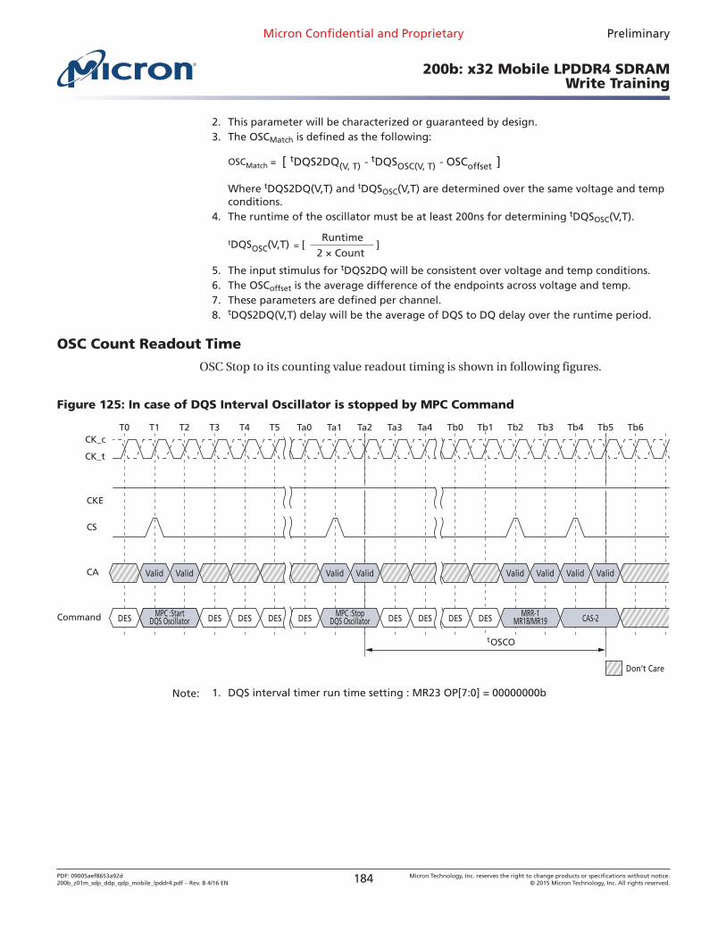
2. This parameter will be characterized or guaranteed by design.3. The OSCMatch is defined as the following:
OSCMatch = [ ]tDQS2DQ(V, T) - tDQSOSC(V, T) - OSCoffset
Where tDQS2DQ(V,T) and tDQSOSC(V,T) are determined over the same voltage and tempconditions.
4. The runtime of the oscillator must be at least 200ns for determining tDQSOSC(V,T).
tDQSOSC(V,T) = [ ]Runtime
2 × Count
5. The input stimulus for tDQS2DQ will be consistent over voltage and temp conditions.6. The OSCoffset is the average difference of the endpoints across voltage and temp.7. These parameters are defined per channel.8. tDQS2DQ(V,T) delay will be the average of DQS to DQ delay over the runtime period.
OSC Count Readout Time
OSC Stop to its counting value readout timing is shown in following figures.
Figure 125: In case of DQS Interval Oscillator is stopped by MPC Command
T0
CK_t
CK_cT1 T2 T3 Tb5
CA
T4 Tb0Ta3 Tb1 Tb4Tb2Ta0 Ta1 Ta2
Command
CS
CKE
Ta4T5 Tb3 Tb6
DES
Valid Valid
MR Write-2 DESDES
Valid Valid
MPC :StartDQS Oscillator DES DES DES
Valid Valid
DESMPC :StopDQS Oscillator CAS-2
Valid Valid
MRR-1MR18/MR19DES DES
tOSCO
Don’t Care
Note: 1. DQS interval timer run time setting : MR23 OP[7:0] = 00000000b
Micron Confidential and Proprietary Preliminary
200b: x32 Mobile LPDDR4 SDRAMWrite Training
PDF: 09005aef8653a92d200b_z01m_sdp_ddp_qdp_mobile_lpddr4.pdf – Rev. B 4/16 EN 184 Micron Technology, Inc. reserves the right to change products or specifications without notice.
© 2015 Micron Technology, Inc. All rights reserved.
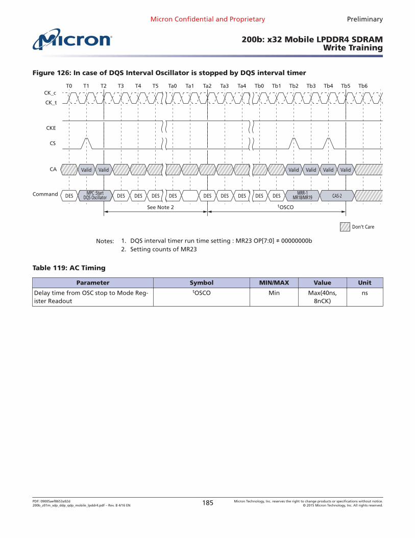
Figure 126: In case of DQS Interval Oscillator is stopped by DQS interval timer
T0
CK_t
CK_cT1 T2 T3 Tb5
CA
T4 Tb0Ta3 Tb1 Tb4Tb2Ta0 Ta1 Ta2
Command
CS
CKE
Ta4T5 Tb3 Tb6
DES DESDES DES DES DES
Valid Valid
DES MRR-1MR18/MR19DES DES
Don’t Care
tOSCOSee Note 2
MR Write-2
Valid Valid
MPC :StartDQS Oscillator CAS-2
Valid
DESDES
Valid
Notes: 1. DQS interval timer run time setting : MR23 OP[7:0] ≠ 00000000b2. Setting counts of MR23
Table 119: AC Timing
Parameter Symbol MIN/MAX Value Unit
Delay time from OSC stop to Mode Reg-ister Readout
tOSCO Min Max(40ns,8nCK)
ns
Micron Confidential and Proprietary Preliminary
200b: x32 Mobile LPDDR4 SDRAMWrite Training
PDF: 09005aef8653a92d200b_z01m_sdp_ddp_qdp_mobile_lpddr4.pdf – Rev. B 4/16 EN 185 Micron Technology, Inc. reserves the right to change products or specifications without notice.
© 2015 Micron Technology, Inc. All rights reserved.
Thermal OffsetBecause of tight thermal coupling, hot spots on an SOC can induce thermal gradientsacross the device. Because these hot spots may not be located near the thermal sensor,the temperature compensated self refresh (TCSR) circuit may not generate enough re-fresh cycles to guarantee memory retention. To address this shortcoming, the controllercan provide a thermal offset that the memory can use to adjust its TCSR circuit to en-sure reliable operation.
This thermal offset is provided through MR4 OP[6:5] to either or both channels. Thistemperature offset may modify refresh behaviour for the channel to which the offset isprovided. It will take a maximum of 200μs to have the change reflected in MR4 OP[2:0]for the channel to which the offset is provided. If the induced thermal gradient from thedevice temperature sensor location to the hot spot location of the controller is greaterthan 15°C, self refresh mode will not reliably maintain memory contents.
To accurately determine the temperature gradient between the memory thermal sensorand the induced hot spot, the memory thermal sensor location must be provided to thecontroller.
Support of the thermal offset function is optional. Please refer to the vendor data sheetto determine if this function is supported.
Temperature SensorThe device has a temperature sensor that can be read from MR4. This sensor can beused to determine the appropriate refresh rate, to determine whether AC timing de-rat-ing is required at an elevated temperature range, and to monitor the operating tempera-ture. Either the temperature sensor or the device TOPER can be used to determine if op-erating temperature requirements are being met.
The device monitors device temperature and updates MR4 according to tTSI. Upon exit-ing self refresh or power-down, the device temperature status bits shall be no older thantTSI.
When using the temperature sensor, the actual device case temperature may be higherthan the TOPER specification that applies to standard or elevated temperature ranges.For example, TCASE may be above 85°C when MR4[2:0] = b011. The device enables a 2°Ctemperature margin between the point when the device updates the MR4 value and thepoint when the controller reconfigures the system accordingly. When performing tightthermal coupling of the device to external hot spots, the maximum device temperaturemay be higher than indicated by MR4.
To ensure proper operation when using the temperature sensor, consider the following:
• TempGradient is the maximum temperature gradient experienced by the device at thetemperature of interest over a range of 2°C.
• ReadInterval is the time period between MR4 reads from the system.• TempSensorInterval (tTSI) is the maximum delay between the internal updates of
MR4.• SysRespDelay is the maximum time between a read of MR4 and a response from the
system.
In order to determine the required frequency of polling MR4, the system uses the Temp-Gradient and the maximum response time of the system in the following equation:
Micron Confidential and Proprietary Preliminary
200b: x32 Mobile LPDDR4 SDRAMThermal Offset
PDF: 09005aef8653a92d200b_z01m_sdp_ddp_qdp_mobile_lpddr4.pdf – Rev. B 4/16 EN 186 Micron Technology, Inc. reserves the right to change products or specifications without notice.
© 2015 Micron Technology, Inc. All rights reserved.
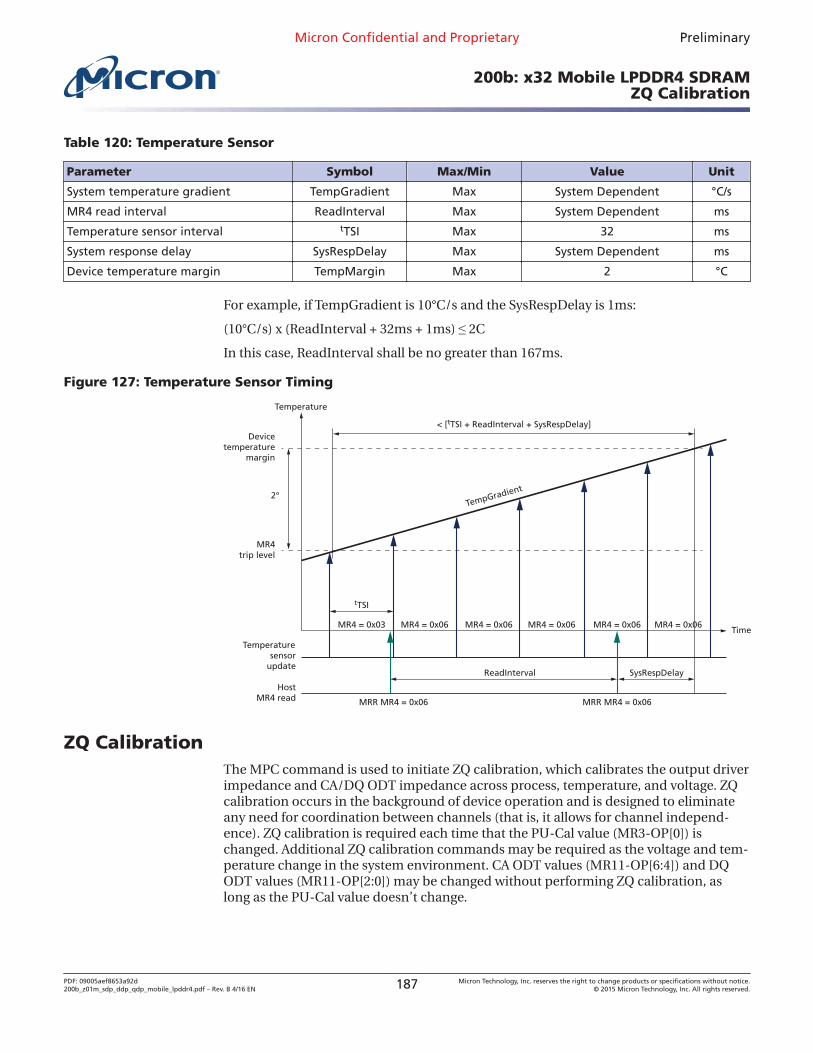
Table 120: Temperature Sensor
Parameter Symbol Max/Min Value Unit
System temperature gradient TempGradient Max System Dependent °C/s
MR4 read interval ReadInterval Max System Dependent ms
Temperature sensor interval tTSI Max 32 ms
System response delay SysRespDelay Max System Dependent ms
Device temperature margin TempMargin Max 2 °C
For example, if TempGradient is 10°C/s and the SysRespDelay is 1ms:
(10°C/s) x (ReadInterval + 32ms + 1ms) ≤ 2C
In this case, ReadInterval shall be no greater than 167ms.
Figure 127: Temperature Sensor Timing
Temperature
< [tTSI + ReadInterval + SysRespDelay]
ReadInterval
tTSI
SysRespDelay
MR4 = 0x03 MR4 = 0x06 MR4 = 0x06 MR4 = 0x06 MR4 = 0x06
MRR MR4 = 0x06MRR MR4 = 0x06
MR4 = 0x06Time
Devicetemperature
margin
Temperaturesensor
update
HostMR4 read
MR4trip level
2°TempGradient
ZQ CalibrationThe MPC command is used to initiate ZQ calibration, which calibrates the output driverimpedance and CA/DQ ODT impedance across process, temperature, and voltage. ZQcalibration occurs in the background of device operation and is designed to eliminateany need for coordination between channels (that is, it allows for channel independ-ence). ZQ calibration is required each time that the PU-Cal value (MR3-OP[0]) ischanged. Additional ZQ calibration commands may be required as the voltage and tem-perature change in the system environment. CA ODT values (MR11-OP[6:4]) and DQODT values (MR11-OP[2:0]) may be changed without performing ZQ calibration, aslong as the PU-Cal value doesn’t change.
Micron Confidential and Proprietary Preliminary
200b: x32 Mobile LPDDR4 SDRAMZQ Calibration
PDF: 09005aef8653a92d200b_z01m_sdp_ddp_qdp_mobile_lpddr4.pdf – Rev. B 4/16 EN 187 Micron Technology, Inc. reserves the right to change products or specifications without notice.
© 2015 Micron Technology, Inc. All rights reserved.
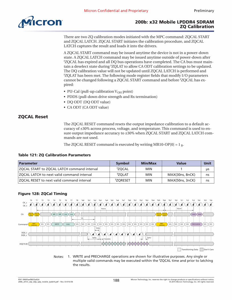
There are two ZQ calibration modes initiated with the MPC command: ZQCAL STARTand ZQCAL LATCH. ZQCAL START initiates the calibration procedure, and ZQCALLATCH captures the result and loads it into the drivers.
A ZQCAL START command may be issued anytime the device is not in a power-downstate. A ZQCAL LATCH command may be issued anytime outside of power-down aftertZQCAL has expired and all DQ bus operations have completed. The CA bus must main-tain a deselect state during tZQLAT to allow CA ODT calibration settings to be updated.The DQ calibration value will not be updated until ZQCAL LATCH is performed andtZQLAT has been met. The following mode register fields that modify I/O parameterscannot be changed following a ZQCAL START command and before tZQCAL has ex-pired:
• PU-Cal (pull-up calibration VOH point)• PDDS (pull-down drive strength and Rx termination)• DQ ODT (DQ ODT value)• CA ODT (CA ODT value)
ZQCAL Reset
The ZQCAL RESET command resets the output impedance calibration to a default ac-curacy of ±30% across process, voltage, and temperature. This command is used to en-sure output impedance accuracy to ±30% when ZQCAL START and ZQCAL LATCH com-mands are not used.
The ZQCAL RESET command is executed by writing MR10-OP[0] = 1 B.
Table 121: ZQ Calibration Parameters
Parameter Symbol Min/Max Value Unit
ZQCAL START to ZQCAL LATCH command interval tZQCAL MIN 1 μs
ZQCAL LATCH to next valid command interval tZQLAT MIN MAX(30ns, 8nCK) ns
ZQCAL RESET to next valid command interval tZQRESET MIN MAX(50ns, 3nCK) ns
Figure 128: ZQCal Timing
T0 T1 T2 T3 T5 T7T4 T6 T8 Ta0 Ta2 Ta4Ta1 Ta3 Ta5CK_c
CK_t
CA
Command
tZQCAL
WL
tZQLAT
MPCtrain/cal
MPCtrain/cal
DQS_cDQS_t
WRITE
WRZQCALstart
ZQCALstart
ZQCALlatch
ZQCALlatch
WR
CAS2
CAS CAS
DES DES DES DESDES DES DES DES DES DES DES DES DES DESDES DES DES DESDES DES DES DES
Valid
PRECHARGE
Valid
Don’t Care
DQ[15:0]
Ta6 Tc0 Tc2 Tc4Tc1 Tc3 Tc5 Tc6Ta7 Tb2 Tb4Tb3 Tb5 Tb6 Tb7Tb0 Tb1
tWPST
tDQSS
tDQS2DQ
Transitioning Data
tWPRE
Notes: 1. WRITE and PRECHARGE operations are shown for illustrative purposes. Any single ormultiple valid commands may be executed within the tZQCAL time and prior to latchingthe results.
Micron Confidential and Proprietary Preliminary
200b: x32 Mobile LPDDR4 SDRAMZQ Calibration
PDF: 09005aef8653a92d200b_z01m_sdp_ddp_qdp_mobile_lpddr4.pdf – Rev. B 4/16 EN 188 Micron Technology, Inc. reserves the right to change products or specifications without notice.
© 2015 Micron Technology, Inc. All rights reserved.
2. Before the ZQCAL LATCH command can be executed, any prior commands that utilizethe DQ bus must have completed. WRITE commands with DQ termination must be givenenough time to turn off the DQ ODT before issuing the ZQCAL LATCH command. Seethe ODT section for ODT timing.
Multichannel Considerations
The device includes a single ZQ pin and associated ZQ calibration circuitry. Calibrationvalues from this circuit will be used by both channels according to the following proto-col:
• The ZQCAL START command can be issued to either or both channels.• The ZQCAL START command can be issued when either or both channels are execut-
ing other commands, and other commands can be issued during tZQCAL.• The ZQCAL START command can be issued to both channels simultaneously.• The ZQCAL START command will begin the calibration unless a previously requested
ZQ calibration is in progress.• If the ZQCAL START command is received while a ZQ calibration is in progress, the
command will be ignored and the in-progress calibration will not be interrupted.• The ZQCAL LATCH command is required for each channel.• The ZQCAL LATCH command can be issued to both channels simultaneously.• The ZQCAL LATCH command will latch results of the most recent ZQCAL START
command provided tZQCAL has been met.• ZQCAL LATCH commands that do not meet tZQCAL will latch the results of the most
recently completed ZQ calibration.• The ZQRESET MRW commands will only reset the calibration values for the channel
issuing the command.
In compliance with complete channel independence, either channel may issue ZQCALSTART and ZQCAL LATCH commands as needed without regard to the state of the otherchannel.
ZQ External Resistor, Tolerance, and Capacitive Loading
To use the ZQ calibration function, a 240 ohm, ±1% tolerance external resistor must beconnected between the ZQ pin and VDDQ.
If the system configuration shares the CA bus to form a x32 (or wider) channel, the ZQpin of each die’s x16 channel must use a separate ZQCAL resistor.
If the system configuration has more than one rank, and if the ZQ pins of both ranks areattached to a single resistor, then the SDRAM controller must ensure that the ZQCAL'sdon’t overlap.
The total capacitive loading on the ZQ pin must be limited to 5pF. For example, if a sys-tem configuration shares a CA bus between n channels to form an n x16 wide bus, andno means are available to control the ZQCAL separately for each channel (that is, sepa-rate CS, CKE, or CK), then each x16 channel must have a separate ZQCAL resistor. For ax32, two-rank system, each x16 channel must have its own ZQCAL resistor, but theZQCAL resistor can be shared between ranks on each x16 channel. In this configuration,the CS signal can be used to ensure that the ZQCAL commands for Rank[0] and Rank[1]don’t overlap.
Micron Confidential and Proprietary Preliminary
200b: x32 Mobile LPDDR4 SDRAMZQ Calibration
PDF: 09005aef8653a92d200b_z01m_sdp_ddp_qdp_mobile_lpddr4.pdf – Rev. B 4/16 EN 189 Micron Technology, Inc. reserves the right to change products or specifications without notice.
© 2015 Micron Technology, Inc. All rights reserved.
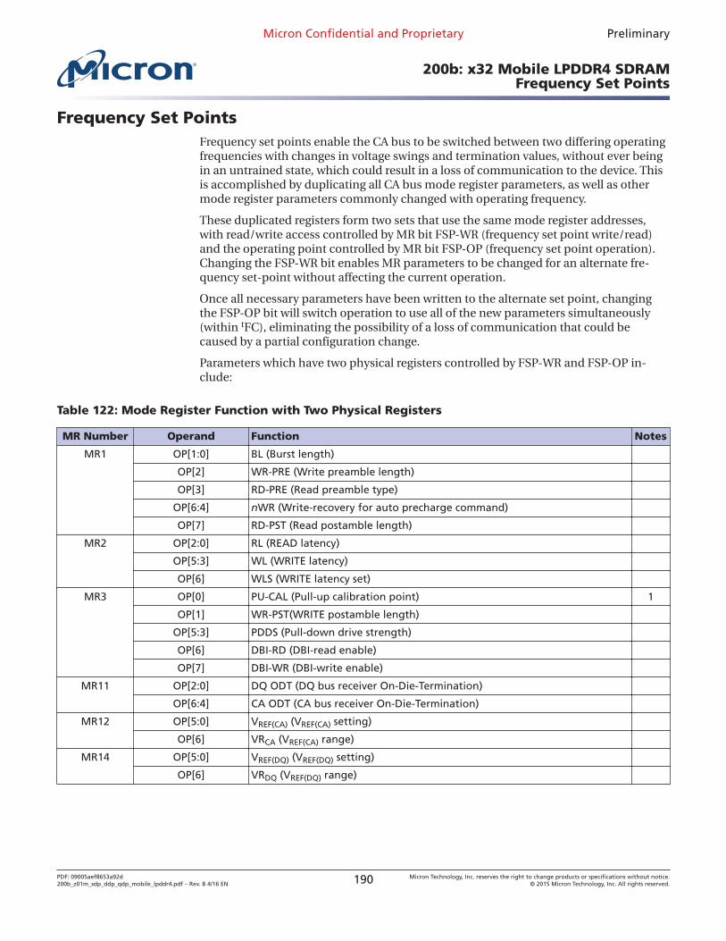
Frequency Set PointsFrequency set points enable the CA bus to be switched between two differing operatingfrequencies with changes in voltage swings and termination values, without ever beingin an untrained state, which could result in a loss of communication to the device. Thisis accomplished by duplicating all CA bus mode register parameters, as well as othermode register parameters commonly changed with operating frequency.
These duplicated registers form two sets that use the same mode register addresses,with read/write access controlled by MR bit FSP-WR (frequency set point write/read)and the operating point controlled by MR bit FSP-OP (frequency set point operation).Changing the FSP-WR bit enables MR parameters to be changed for an alternate fre-quency set-point without affecting the current operation.
Once all necessary parameters have been written to the alternate set point, changingthe FSP-OP bit will switch operation to use all of the new parameters simultaneously(within tFC), eliminating the possibility of a loss of communication that could becaused by a partial configuration change.
Parameters which have two physical registers controlled by FSP-WR and FSP-OP in-clude:
Table 122: Mode Register Function with Two Physical Registers
MR Number Operand Function Notes
MR1 OP[1:0] BL (Burst length)
OP[2] WR-PRE (Write preamble length)
OP[3] RD-PRE (Read preamble type)
OP[6:4] nWR (Write-recovery for auto precharge command)
OP[7] RD-PST (Read postamble length)
MR2 OP[2:0] RL (READ latency)
OP[5:3] WL (WRITE latency)
OP[6] WLS (WRITE latency set)
MR3 OP[0] PU-CAL (Pull-up calibration point) 1
OP[1] WR-PST(WRITE postamble length)
OP[5:3] PDDS (Pull-down drive strength)
OP[6] DBI-RD (DBI-read enable)
OP[7] DBI-WR (DBI-write enable)
MR11 OP[2:0] DQ ODT (DQ bus receiver On-Die-Termination)
OP[6:4] CA ODT (CA bus receiver On-Die-Termination)
MR12 OP[5:0] VREF(CA) (VREF(CA) setting)
OP[6] VRCA (VREF(CA) range)
MR14 OP[5:0] VREF(DQ) (VREF(DQ) setting)
OP[6] VRDQ (VREF(DQ) range)
Micron Confidential and Proprietary Preliminary
200b: x32 Mobile LPDDR4 SDRAMFrequency Set Points
PDF: 09005aef8653a92d200b_z01m_sdp_ddp_qdp_mobile_lpddr4.pdf – Rev. B 4/16 EN 190 Micron Technology, Inc. reserves the right to change products or specifications without notice.
© 2015 Micron Technology, Inc. All rights reserved.
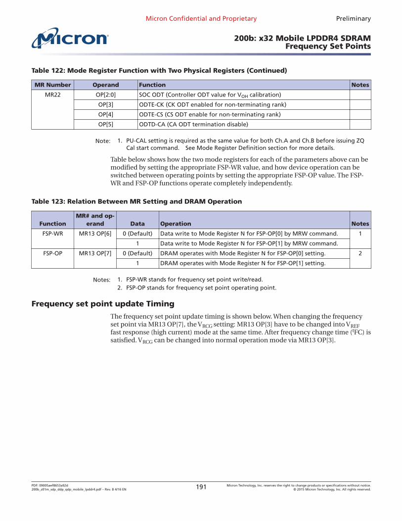
Table 122: Mode Register Function with Two Physical Registers (Continued)
MR Number Operand Function Notes
MR22 OP[2:0] SOC ODT (Controller ODT value for VOH calibration)
OP[3] ODTE-CK (CK ODT enabled for non-terminating rank)
OP[4] ODTE-CS (CS ODT enable for non-terminating rank)
OP[5] ODTD-CA (CA ODT termination disable)
Note: 1. PU-CAL setting is required as the same value for both Ch.A and Ch.B before issuing ZQCal start command. See Mode Register Definition section for more details.
Table below shows how the two mode registers for each of the parameters above can bemodified by setting the appropriate FSP-WR value, and how device operation can beswitched between operating points by setting the appropriate FSP-OP value. The FSP-WR and FSP-OP functions operate completely independently.
Table 123: Relation Between MR Setting and DRAM Operation
FunctionMR# and op-
erand Data Operation Notes
FSP-WR MR13 OP[6] 0 (Default) Data write to Mode Register N for FSP-OP[0] by MRW command. 1
1 Data write to Mode Register N for FSP-OP[1] by MRW command.
FSP-OP MR13 OP[7] 0 (Default) DRAM operates with Mode Register N for FSP-OP[0] setting. 2
1 DRAM operates with Mode Register N for FSP-OP[1] setting.
Notes: 1. FSP-WR stands for frequency set point write/read.2. FSP-OP stands for frequency set point operating point.
Frequency set point update Timing
The frequency set point update timing is shown below. When changing the frequencyset point via MR13 OP[7], the VRCG setting: MR13 OP[3] have to be changed into VREFfast response (high current) mode at the same time. After frequency change time (tFC) issatisfied. VRCG can be changed into normal operation mode via MR13 OP[3].
Micron Confidential and Proprietary Preliminary
200b: x32 Mobile LPDDR4 SDRAMFrequency Set Points
PDF: 09005aef8653a92d200b_z01m_sdp_ddp_qdp_mobile_lpddr4.pdf – Rev. B 4/16 EN 191 Micron Technology, Inc. reserves the right to change products or specifications without notice.
© 2015 Micron Technology, Inc. All rights reserved.
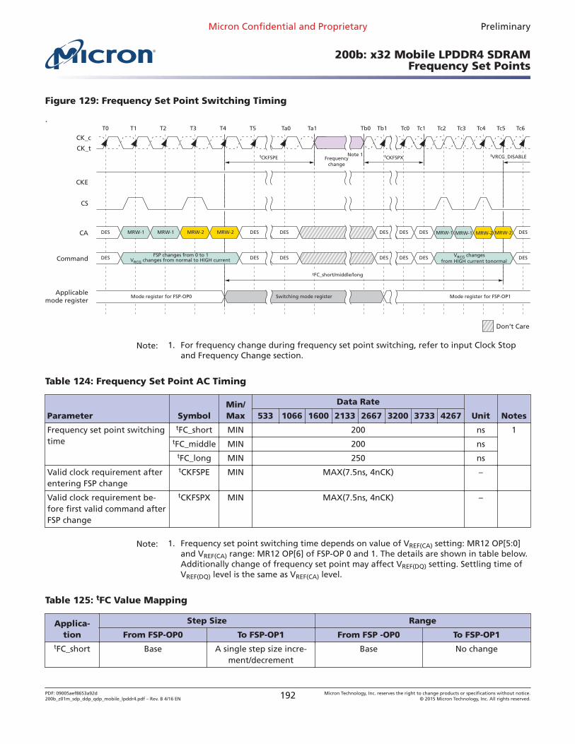
Figure 129: Frequency Set Point Switching Timing
.T0 T1 T2 T3 T4 T5 Ta0 Ta1 Tb1Tb0
CK_c
CK_t
Tc0 Tc6Tc4 Tc5Tc1 Tc3Tc2
Don’t Care
CS
CA
Command
CKE
tCKFSPE Frequencychange
tCKFSPX tVRCG_DISABLENote 1
MRW-2 DES
DES
Mode register for FSP-OP1Switching mode register
DES
DES
DES
DES
DES
DES
DES
DES
DES
DES
DES
DES
MRW-2MRW-1MRW-1
FSP changes from 0 to 1VRCG changes from normal to HIGH current
MRW-2MRW-2MRW-1MRW-1
VRCG changes from HIGH current tonormal
Applicablemode register
tFC_short/middle/long
Mode register for FSP-OP0
Note: 1. For frequency change during frequency set point switching, refer to input Clock Stopand Frequency Change section.
Table 124: Frequency Set Point AC Timing
Parameter SymbolMin/Max
Data Rate
Unit Notes533 1066 1600 2133 2667 3200 3733 4267
Frequency set point switchingtime
tFC_short MIN 200 ns 1tFC_middle MIN 200 ns
tFC_long MIN 250 ns
Valid clock requirement afterentering FSP change
tCKFSPE MIN MAX(7.5ns, 4nCK) –
Valid clock requirement be-fore first valid command afterFSP change
tCKFSPX MIN MAX(7.5ns, 4nCK) –
Note: 1. Frequency set point switching time depends on value of VREF(CA) setting: MR12 OP[5:0]and VREF(CA) range: MR12 OP[6] of FSP-OP 0 and 1. The details are shown in table below.Additionally change of frequency set point may affect VREF(DQ) setting. Settling time ofVREF(DQ) level is the same as VREF(CA) level.
Table 125: tFC Value Mapping
Applica-tion
Step Size Range
From FSP-OP0 To FSP-OP1 From FSP -OP0 To FSP-OP1tFC_short Base A single step size incre-
ment/decrementBase No change
Micron Confidential and Proprietary Preliminary
200b: x32 Mobile LPDDR4 SDRAMFrequency Set Points
PDF: 09005aef8653a92d200b_z01m_sdp_ddp_qdp_mobile_lpddr4.pdf – Rev. B 4/16 EN 192 Micron Technology, Inc. reserves the right to change products or specifications without notice.
© 2015 Micron Technology, Inc. All rights reserved.
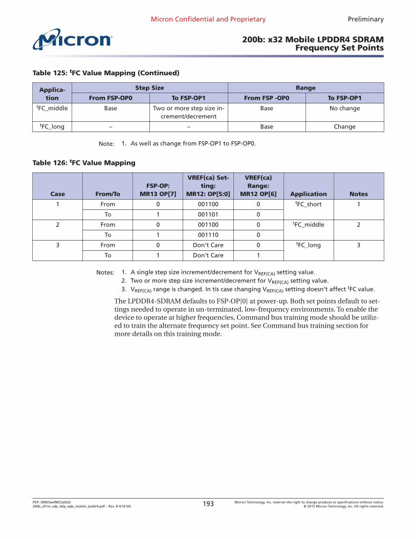
Table 125: tFC Value Mapping (Continued)
Applica-tion
Step Size Range
From FSP-OP0 To FSP-OP1 From FSP -OP0 To FSP-OP1tFC_middle Base Two or more step size in-
crement/decrementBase No change
tFC_long – – Base Change
Note: 1. As well as change from FSP-OP1 to FSP-OP0.
Table 126: tFC Value Mapping
Case From/ToFSP-OP:
MR13 OP[7]
VREF(ca) Set-ting:
MR12: OP[5:0]
VREF(ca)Range:
MR12 OP[6] Application Notes
1 From 0 001100 0 tFC_short 1
To 1 001101 0
2 From 0 001100 0 tFC_middle 2
To 1 001110 0
3 From 0 Don't Care 0 tFC_long 3
To 1 Don't Care 1
Notes: 1. A single step size increment/decrement for VREF(CA) setting value.2. Two or more step size increment/decrement for VREF(CA) setting value.3. VREF(CA) range is changed. In tis case changing VREF(CA) setting doesn’t affect tFC value.
The LPDDR4-SDRAM defaults to FSP-OP[0] at power-up. Both set points default to set-tings needed to operate in un-terminated, low-frequency environments. To enable thedevice to operate at higher frequencies, Command bus training mode should be utiliz-ed to train the alternate frequency set point. See Command bus training section formore details on this training mode.
Micron Confidential and Proprietary Preliminary
200b: x32 Mobile LPDDR4 SDRAMFrequency Set Points
PDF: 09005aef8653a92d200b_z01m_sdp_ddp_qdp_mobile_lpddr4.pdf – Rev. B 4/16 EN 193 Micron Technology, Inc. reserves the right to change products or specifications without notice.
© 2015 Micron Technology, Inc. All rights reserved.
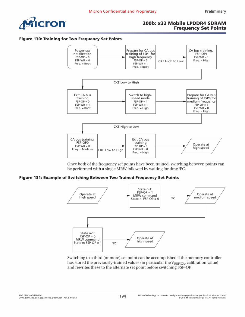
Figure 130: Training for Two Frequency Set Points
Power-up/Initialization
FSP-OP = 0FSP-WR = 0Freq. = Boot
Prepare for CA bustraining of FSP1 for
high frequencyFSP-OP = 0FSP-WR = 1Freq. = Boot
CA bus training, FSP-OP1
FSP-WR = 1Freq. = High
Exit CA bustraining
FSP-OP = 0FSP-WR = 1Freq. = Boot
Switch to high-speed mode
FSP-OP = 1FSP-WR = 1Freq. = High
Prepare for CA bustraining of FSP0 formedium frequency
FSP-OP = 1FSP-WR = 0Freq. = High
CA bus training,FSP-OP0
FSP-WR = 0Freq. = Medium
Exit CA bustraining
FSP-OP = 1FSP-WR = 0Freq. = High
Operate athigh speed
CKE Low to High
CKE Low to High
CKE High to Low
CKE High to Low
Once both of the frequency set points have been trained, switching between points canbe performed with a single MRW followed by waiting for time tFC.
Figure 131: Example of Switching Between Two Trained Frequency Set Points
State n-1:FSP-OP = 1
MRW commandState n: FSP-OP = 0
State n-1:FSP-OP = 0
MRW commandState n: FSP-OP = 1
Operate athigh speed tFC
tFC
Operate athigh speed
Operate atmedium speed
Switching to a third (or more) set point can be accomplished if the memory controllerhas stored the previously-trained values (in particular the VREF(CA) calibration value)and rewrites these to the alternate set point before switching FSP-OP.
Micron Confidential and Proprietary Preliminary
200b: x32 Mobile LPDDR4 SDRAMFrequency Set Points
PDF: 09005aef8653a92d200b_z01m_sdp_ddp_qdp_mobile_lpddr4.pdf – Rev. B 4/16 EN 194 Micron Technology, Inc. reserves the right to change products or specifications without notice.
© 2015 Micron Technology, Inc. All rights reserved.
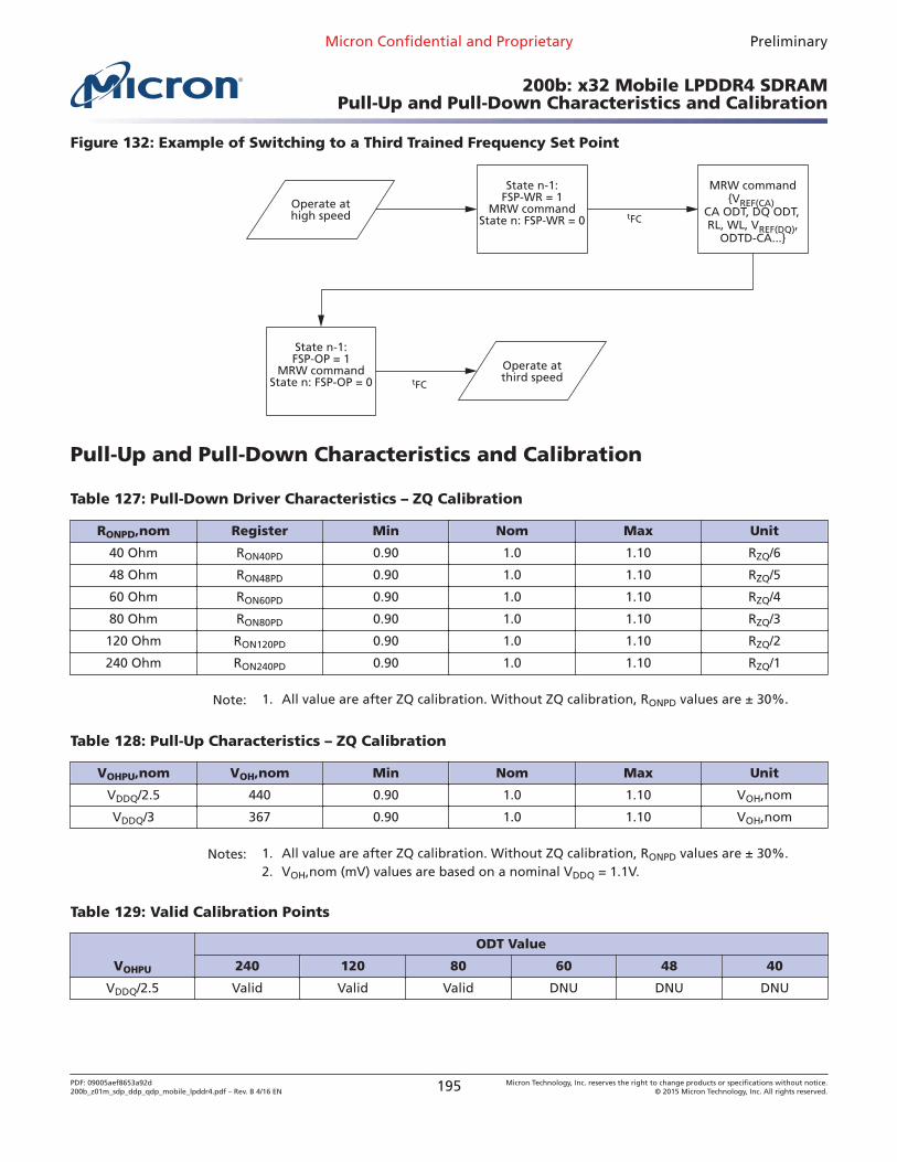
Figure 132: Example of Switching to a Third Trained Frequency Set Point
State n-1:FSP-WR = 1
MRW commandState n: FSP-WR = 0
State n-1:FSP-OP = 1
MRW commandState n: FSP-OP = 0
MRW command{VREF(CA)
CA ODT, DQ ODT,RL, WL, VREF(DQ),
ODTD-CA...}
Operate athigh speed tFC
tFC
Operate atthird speed
Pull-Up and Pull-Down Characteristics and Calibration
Table 127: Pull-Down Driver Characteristics – ZQ Calibration
RONPD,nom Register Min Nom Max Unit
40 Ohm RON40PD 0.90 1.0 1.10 RZQ/6
48 Ohm RON48PD 0.90 1.0 1.10 RZQ/5
60 Ohm RON60PD 0.90 1.0 1.10 RZQ/4
80 Ohm RON80PD 0.90 1.0 1.10 RZQ/3
120 Ohm RON120PD 0.90 1.0 1.10 RZQ/2
240 Ohm RON240PD 0.90 1.0 1.10 RZQ/1
Note: 1. All value are after ZQ calibration. Without ZQ calibration, RONPD values are ± 30%.
Table 128: Pull-Up Characteristics – ZQ Calibration
VOHPU,nom VOH,nom Min Nom Max Unit
VDDQ/2.5 440 0.90 1.0 1.10 VOH,nom
VDDQ/3 367 0.90 1.0 1.10 VOH,nom
Notes: 1. All value are after ZQ calibration. Without ZQ calibration, RONPD values are ± 30%.2. VOH,nom (mV) values are based on a nominal VDDQ = 1.1V.
Table 129: Valid Calibration Points
VOHPU
ODT Value
240 120 80 60 48 40
VDDQ/2.5 Valid Valid Valid DNU DNU DNU
Micron Confidential and Proprietary Preliminary
200b: x32 Mobile LPDDR4 SDRAMPull-Up and Pull-Down Characteristics and Calibration
PDF: 09005aef8653a92d200b_z01m_sdp_ddp_qdp_mobile_lpddr4.pdf – Rev. B 4/16 EN 195 Micron Technology, Inc. reserves the right to change products or specifications without notice.
© 2015 Micron Technology, Inc. All rights reserved.
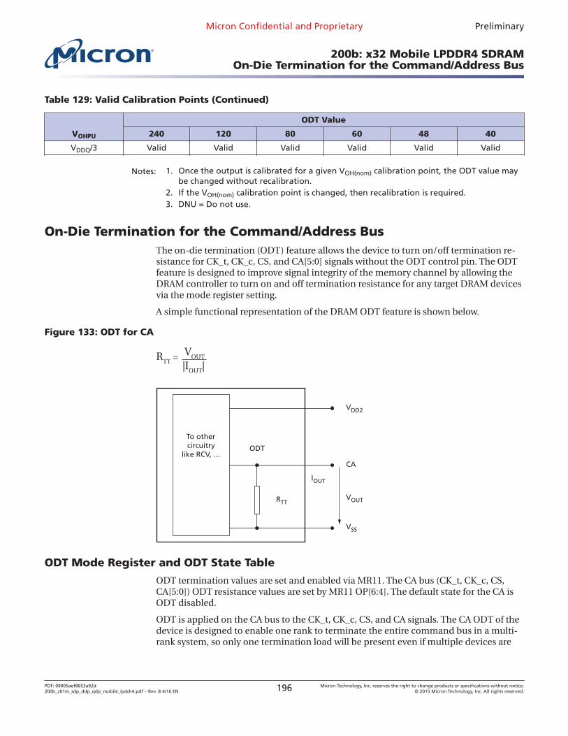
Table 129: Valid Calibration Points (Continued)
VOHPU
ODT Value
240 120 80 60 48 40
VDDQ/3 Valid Valid Valid Valid Valid Valid
Notes: 1. Once the output is calibrated for a given VOH(nom) calibration point, the ODT value maybe changed without recalibration.
2. If the VOH(nom) calibration point is changed, then recalibration is required.3. DNU = Do not use.
On-Die Termination for the Command/Address BusThe on-die termination (ODT) feature allows the device to turn on/off termination re-sistance for CK_t, CK_c, CS, and CA[5:0] signals without the ODT control pin. The ODTfeature is designed to improve signal integrity of the memory channel by allowing theDRAM controller to turn on and off termination resistance for any target DRAM devicesvia the mode register setting.
A simple functional representation of the DRAM ODT feature is shown below.
Figure 133: ODT for CA
RTT
= VOUT |I
OUT|
To othercircuitry
like RCV, ...ODT
RTT
IOUT
CA
VOUT
VSS
VDD2
ODT Mode Register and ODT State Table
ODT termination values are set and enabled via MR11. The CA bus (CK_t, CK_c, CS,CA[5:0]) ODT resistance values are set by MR11 OP[6:4]. The default state for the CA isODT disabled.
ODT is applied on the CA bus to the CK_t, CK_c, CS, and CA signals. The CA ODT of thedevice is designed to enable one rank to terminate the entire command bus in a multi-rank system, so only one termination load will be present even if multiple devices are
Micron Confidential and Proprietary Preliminary
200b: x32 Mobile LPDDR4 SDRAMOn-Die Termination for the Command/Address Bus
PDF: 09005aef8653a92d200b_z01m_sdp_ddp_qdp_mobile_lpddr4.pdf – Rev. B 4/16 EN 196 Micron Technology, Inc. reserves the right to change products or specifications without notice.
© 2015 Micron Technology, Inc. All rights reserved.
sharing the command signals. For this reason, CA ODT remains on, even when the de-vice is in the power-down or self refresh power-down state.
The die has a bond pad (ODT_CA) for multirank operations. When the ODT_CA pad isLOW, the die will not terminate the CA bus regardless of the state of the mode registerCA ODT bits (MR11 OP[6:4]). If, however, the ODT_CA bond pad is HIGH and the moderegister CA ODT bits are enabled, the die will terminate the CA bus with the ODT valuesfound in MR11 OP[6:4]. In a multirank system, the terminating rank should be trainedfirst, followed by the non-terminating rank(s).
Table 130: Command Bus ODT State
CA ODTMR11[6:4]
ODT_CABond Pad
ODTD-CAMR22 OP[5]
ODTE-CKMR22 OP[3]
ODTE-CSMR22 OP[4]
ODT Statefor CA
ODT Statefor CK
ODT Statefor CS
Disabled1 Valid2 Valid3 Valid3 Valid3 Off Off Off
Valid 3 0 Valid3 0 0 Off Off Off
Valid 3 0 Valid3 0 1 Off Off On
Valid 3 0 Valid3 1 0 Off On Off
Valid 3 0 Valid3 1 1 Off On On
Valid 3 1 0 Valid3 Valid3 On On On
Valid 3 1 1 Valid3 Valid3 Off On On
Notes: 1. Default value.2. Valid = H or L (a defined logic level)3. Valid = 0 or 1.4. The state of ODT_CA is not changed when the device enters power-down mode. This
maintains termination for alternate ranks in multirank systems.
ODT Mode Register and ODT Characteristics
Table 131: ODT DC Electrical Characteristics – up to 3200 Mbps
RZQ Ω ±1% over entire operating range after calibrationMR11 OP[6:4] RTT VOUT Min Nom Max Unit Notes
001b Ω VOL(DC) = 0.1 × VDD2 0.8 1.0 1.1 RZQ/1 1, 2
VOM(DC) = 0.33 × VDD2 0.9 1.0 1.1
VOH(DC) = 0.5 × VDD2 0.9 1.0 1.2
010b Ω VOL(DC) = 0.1 × VDD2 0.8 1.0 1.1 RZQ/2 1, 2
VOM(DC) = 0.33 × VDD2 0.9 1.0 1.1
VOH(DC) = 0.5 × VDD2 0.9 1.0 1.2
011b Ω VOL(DC) = 0.1 × VDD2 0.8 1.0 1.1 RZQ/3 1, 2
VOM(DC) = 0.33 × VDD2 0.9 1.0 1.1
VOH(DC) = 0.5 × VDD2 0.9 1.0 1.2
100b Ω VOL(DC) = 0.1 × VDD2 0.8 1.0 1.1 RZQ/4 1, 2
V OM(DC) = 0.33 × VDD2 0.9 1.0 1.1
VOH(DC) = 0.5 × VDD2 0.9 1.0 1.2
Micron Confidential and Proprietary Preliminary
200b: x32 Mobile LPDDR4 SDRAMOn-Die Termination for the Command/Address Bus
PDF: 09005aef8653a92d200b_z01m_sdp_ddp_qdp_mobile_lpddr4.pdf – Rev. B 4/16 EN 197 Micron Technology, Inc. reserves the right to change products or specifications without notice.
© 2015 Micron Technology, Inc. All rights reserved.
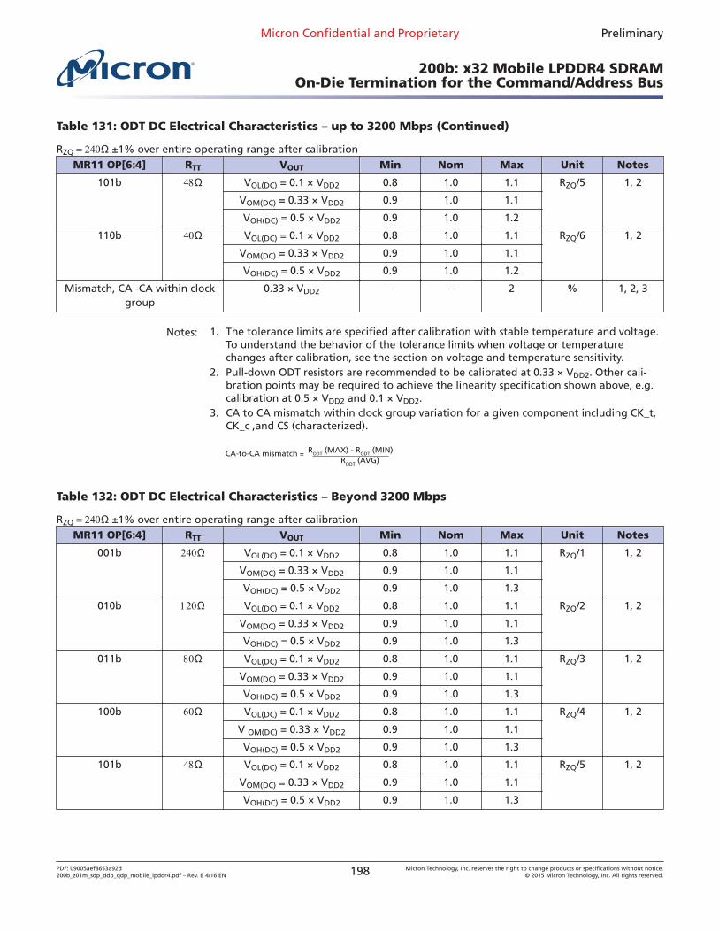
Table 131: ODT DC Electrical Characteristics – up to 3200 Mbps (Continued)
RZQ Ω ±1% over entire operating range after calibrationMR11 OP[6:4] RTT VOUT Min Nom Max Unit Notes
101b Ω VOL(DC) = 0.1 × VDD2 0.8 1.0 1.1 RZQ/5 1, 2
VOM(DC) = 0.33 × VDD2 0.9 1.0 1.1
VOH(DC) = 0.5 × VDD2 0.9 1.0 1.2
110b Ω VOL(DC) = 0.1 × VDD2 0.8 1.0 1.1 RZQ/6 1, 2
VOM(DC) = 0.33 × VDD2 0.9 1.0 1.1
VOH(DC) = 0.5 × VDD2 0.9 1.0 1.2
Mismatch, CA -CA within clockgroup
0.33 × VDD2 – – 2 % 1, 2, 3
Notes: 1. The tolerance limits are specified after calibration with stable temperature and voltage.To understand the behavior of the tolerance limits when voltage or temperaturechanges after calibration, see the section on voltage and temperature sensitivity.
2. Pull-down ODT resistors are recommended to be calibrated at 0.33 × VDD2. Other cali-bration points may be required to achieve the linearity specification shown above, e.g.calibration at 0.5 × VDD2 and 0.1 × VDD2.
3. CA to CA mismatch within clock group variation for a given component including CK_t,CK_c ,and CS (characterized).
CA-to-CA mismatch = RODT (MAX) - RODT (MIN) RODT (AVG)
Table 132: ODT DC Electrical Characteristics – Beyond 3200 Mbps
RZQ Ω ±1% over entire operating range after calibrationMR11 OP[6:4] RTT VOUT Min Nom Max Unit Notes
001b Ω VOL(DC) = 0.1 × VDD2 0.8 1.0 1.1 RZQ/1 1, 2
VOM(DC) = 0.33 × VDD2 0.9 1.0 1.1
VOH(DC) = 0.5 × VDD2 0.9 1.0 1.3
010b Ω VOL(DC) = 0.1 × VDD2 0.8 1.0 1.1 RZQ/2 1, 2
VOM(DC) = 0.33 × VDD2 0.9 1.0 1.1
VOH(DC) = 0.5 × VDD2 0.9 1.0 1.3
011b Ω VOL(DC) = 0.1 × VDD2 0.8 1.0 1.1 RZQ/3 1, 2
VOM(DC) = 0.33 × VDD2 0.9 1.0 1.1
VOH(DC) = 0.5 × VDD2 0.9 1.0 1.3
100b Ω VOL(DC) = 0.1 × VDD2 0.8 1.0 1.1 RZQ/4 1, 2
V OM(DC) = 0.33 × VDD2 0.9 1.0 1.1
VOH(DC) = 0.5 × VDD2 0.9 1.0 1.3
101b Ω VOL(DC) = 0.1 × VDD2 0.8 1.0 1.1 RZQ/5 1, 2
VOM(DC) = 0.33 × VDD2 0.9 1.0 1.1
VOH(DC) = 0.5 × VDD2 0.9 1.0 1.3
Micron Confidential and Proprietary Preliminary
200b: x32 Mobile LPDDR4 SDRAMOn-Die Termination for the Command/Address Bus
PDF: 09005aef8653a92d200b_z01m_sdp_ddp_qdp_mobile_lpddr4.pdf – Rev. B 4/16 EN 198 Micron Technology, Inc. reserves the right to change products or specifications without notice.
© 2015 Micron Technology, Inc. All rights reserved.
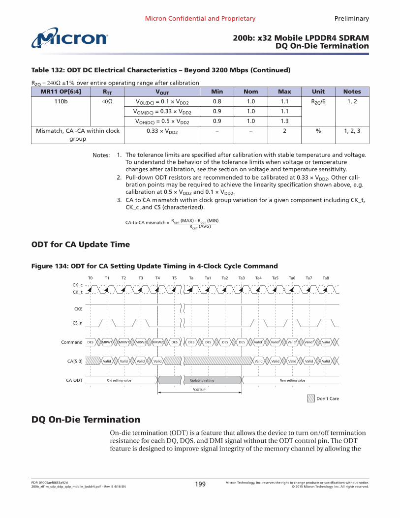
Table 132: ODT DC Electrical Characteristics – Beyond 3200 Mbps (Continued)
RZQ Ω ±1% over entire operating range after calibrationMR11 OP[6:4] RTT VOUT Min Nom Max Unit Notes
110b Ω VOL(DC) = 0.1 × VDD2 0.8 1.0 1.1 RZQ/6 1, 2
VOM(DC) = 0.33 × VDD2 0.9 1.0 1.1
VOH(DC) = 0.5 × VDD2 0.9 1.0 1.3
Mismatch, CA -CA within clockgroup
0.33 × VDD2 – – 2 % 1, 2, 3
Notes: 1. The tolerance limits are specified after calibration with stable temperature and voltage.To understand the behavior of the tolerance limits when voltage or temperaturechanges after calibration, see the section on voltage and temperature sensitivity.
2. Pull-down ODT resistors are recommended to be calibrated at 0.33 × VDD2. Other cali-bration points may be required to achieve the linearity specification shown above, e.g.calibration at 0.5 × VDD2 and 0.1 × VDD2.
3. CA to CA mismatch within clock group variation for a given component including CK_t,CK_c ,and CS (characterized).
CA-to-CA mismatch = RODT (MAX) - RODT (MIN) RODT (AVG)
ODT for CA Update Time
Figure 134: ODT for CA Setting Update Timing in 4-Clock Cycle Command
T0 T1 T2 T3 T4 T5 Ta Ta1 Ta2 Ta3 Ta4 Ta5 Ta6 Ta7 Ta8
CK_c
CK_t
Command
CS_n
CKE
CA[5:0]
tODTUP
Don’t Care
DES MRW1 MRW1 MRW2 MRW2 DES DES DES DES DES Valid1 Valid1 Valid1 Valid1 Valid
Valid Valid Valid Valid Valid Valid Valid Valid Valid
CA ODT Old setting value Updating setting New setting value
DQ On-Die TerminationOn-die termination (ODT) is a feature that allows the device to turn on/off terminationresistance for each DQ, DQS, and DMI signal without the ODT control pin. The ODTfeature is designed to improve signal integrity of the memory channel by allowing the
Micron Confidential and Proprietary Preliminary
200b: x32 Mobile LPDDR4 SDRAMDQ On-Die Termination
PDF: 09005aef8653a92d200b_z01m_sdp_ddp_qdp_mobile_lpddr4.pdf – Rev. B 4/16 EN 199 Micron Technology, Inc. reserves the right to change products or specifications without notice.
© 2015 Micron Technology, Inc. All rights reserved.
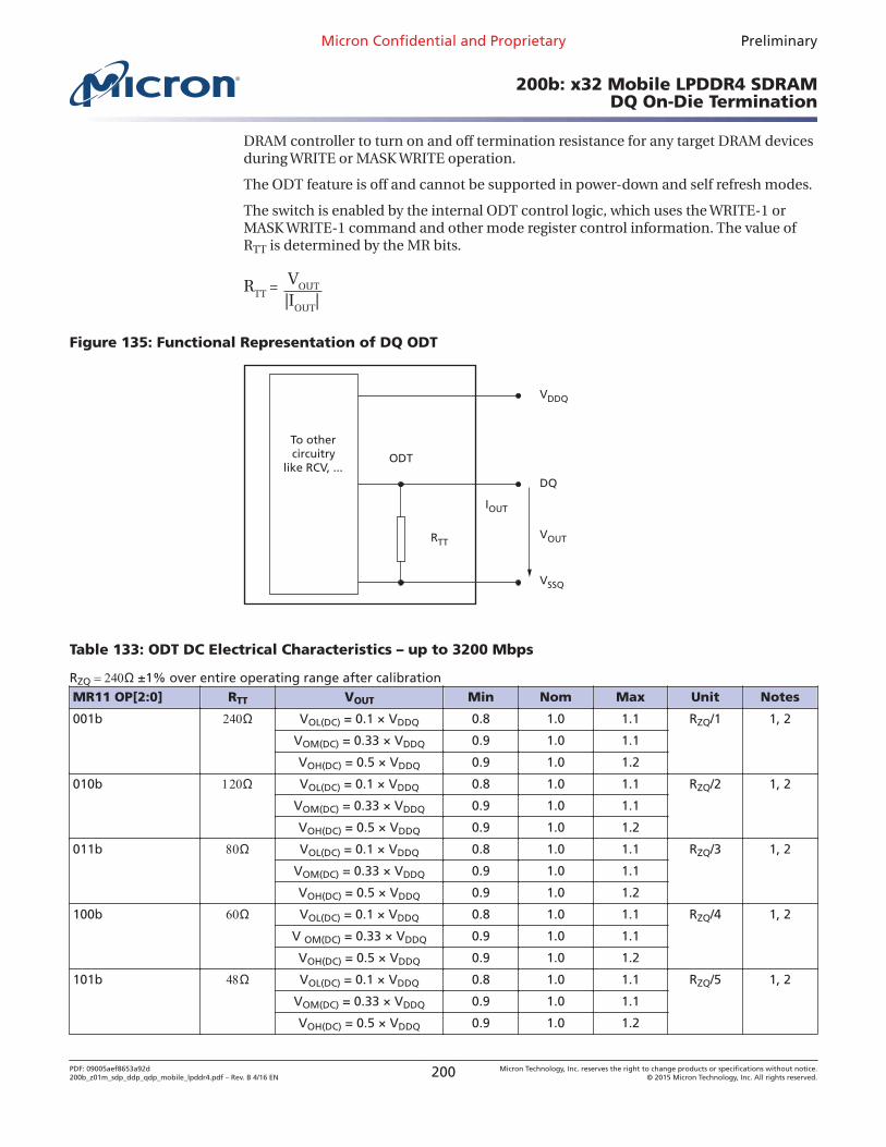
DRAM controller to turn on and off termination resistance for any target DRAM devicesduring WRITE or MASK WRITE operation.
The ODT feature is off and cannot be supported in power-down and self refresh modes.
The switch is enabled by the internal ODT control logic, which uses the WRITE-1 orMASK WRITE-1 command and other mode register control information. The value ofRTT is determined by the MR bits.
RTT
= VOUT |I
OUT|
Figure 135: Functional Representation of DQ ODT
To othercircuitry
like RCV, ...ODT
RTT
IOUT
DQ
VOUT
VSSQ
VDDQ
Table 133: ODT DC Electrical Characteristics – up to 3200 Mbps
RZQ Ω ±1% over entire operating range after calibrationMR11 OP[2:0] RTT VOUT Min Nom Max Unit Notes
001b Ω VOL(DC) = 0.1 × VDDQ 0.8 1.0 1.1 RZQ/1 1, 2
VOM(DC) = 0.33 × VDDQ 0.9 1.0 1.1
VOH(DC) = 0.5 × VDDQ 0.9 1.0 1.2
010b Ω VOL(DC) = 0.1 × VDDQ 0.8 1.0 1.1 RZQ/2 1, 2
VOM(DC) = 0.33 × VDDQ 0.9 1.0 1.1
VOH(DC) = 0.5 × VDDQ 0.9 1.0 1.2
011b Ω VOL(DC) = 0.1 × VDDQ 0.8 1.0 1.1 RZQ/3 1, 2
VOM(DC) = 0.33 × VDDQ 0.9 1.0 1.1
VOH(DC) = 0.5 × VDDQ 0.9 1.0 1.2
100b Ω VOL(DC) = 0.1 × VDDQ 0.8 1.0 1.1 RZQ/4 1, 2
V OM(DC) = 0.33 × VDDQ 0.9 1.0 1.1
VOH(DC) = 0.5 × VDDQ 0.9 1.0 1.2
101b Ω VOL(DC) = 0.1 × VDDQ 0.8 1.0 1.1 RZQ/5 1, 2
VOM(DC) = 0.33 × VDDQ 0.9 1.0 1.1
VOH(DC) = 0.5 × VDDQ 0.9 1.0 1.2
Micron Confidential and Proprietary Preliminary
200b: x32 Mobile LPDDR4 SDRAMDQ On-Die Termination
PDF: 09005aef8653a92d200b_z01m_sdp_ddp_qdp_mobile_lpddr4.pdf – Rev. B 4/16 EN 200 Micron Technology, Inc. reserves the right to change products or specifications without notice.
© 2015 Micron Technology, Inc. All rights reserved.
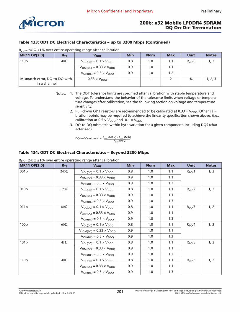
Table 133: ODT DC Electrical Characteristics – up to 3200 Mbps (Continued)
RZQ Ω ±1% over entire operating range after calibrationMR11 OP[2:0] RTT VOUT Min Nom Max Unit Notes
110b Ω VOL(DC) = 0.1 × VDDQ 0.8 1.0 1.1 RZQ/6 1, 2
VOM(DC) = 0.33 × VDDQ 0.9 1.0 1.1
VOH(DC) = 0.5 × VDDQ 0.9 1.0 1.2
Mismatch error, DQ-to-DQ with-in a channel
0.33 × VDDQ – – 2 % 1, 2, 3
Notes: 1. The ODT tolerance limits are specified after calibration with stable temperature andvoltage. To understand the behavior of the tolerance limits when voltage or tempera-ture changes after calibration, see the following section on voltage and temperaturesensitivity.
2. Pull-down ODT resistors are recommended to be calibrated at 0.33 × VDDQ. Other cali-bration points may be required to achieve the linearity specification shown above, (i.e.,calibration at 0.5 × VDDQ and -0.1 × VDDQ.
3. DQ-to-DQ mismatch within byte variation for a given component, including DQS (char-acterized).
DQ-to-DQ mismatch = RODT (MAX) - RODT (MIN) RODT (AVG)
Table 134: ODT DC Electrical Characteristics – Beyond 3200 Mbps
RZQ Ω ±1% over entire operating range after calibrationMR11 OP[2:0] RTT VOUT Min Nom Max Unit Notes
001b Ω VOL(DC) = 0.1 × VDDQ 0.8 1.0 1.1 RZQ/1 1, 2
VOM(DC) = 0.33 × VDDQ 0.9 1.0 1.1
VOH(DC) = 0.5 × VDDQ 0.9 1.0 1.3
010b Ω VOL(DC) = 0.1 × VDDQ 0.8 1.0 1.1 RZQ/2 1, 2
VOM(DC) = 0.33 × VDDQ 0.9 1.0 1.1
VOH(DC) = 0.5 × VDDQ 0.9 1.0 1.3
011b Ω VOL(DC) = 0.1 × VDDQ 0.8 1.0 1.1 RZQ/3 1, 2
VOM(DC) = 0.33 × VDDQ 0.9 1.0 1.1
VOH(DC) = 0.5 × VDDQ 0.9 1.0 1.3
100b Ω VOL(DC) = 0.1 × VDDQ 0.8 1.0 1.1 RZQ/4 1, 2
V OM(DC) = 0.33 × VDDQ 0.9 1.0 1.1
VOH(DC) = 0.5 × VDDQ 0.9 1.0 1.3
101b Ω VOL(DC) = 0.1 × VDDQ 0.8 1.0 1.1 RZQ/5 1, 2
VOM(DC) = 0.33 × VDDQ 0.9 1.0 1.1
VOH(DC) = 0.5 × VDDQ 0.9 1.0 1.3
110b Ω VOL(DC) = 0.1 × VDDQ 0.8 1.0 1.1 RZQ/6 1, 2
VOM(DC) = 0.33 × VDDQ 0.9 1.0 1.1
VOH(DC) = 0.5 × VDDQ 0.9 1.0 1.3
Micron Confidential and Proprietary Preliminary
200b: x32 Mobile LPDDR4 SDRAMDQ On-Die Termination
PDF: 09005aef8653a92d200b_z01m_sdp_ddp_qdp_mobile_lpddr4.pdf – Rev. B 4/16 EN 201 Micron Technology, Inc. reserves the right to change products or specifications without notice.
© 2015 Micron Technology, Inc. All rights reserved.
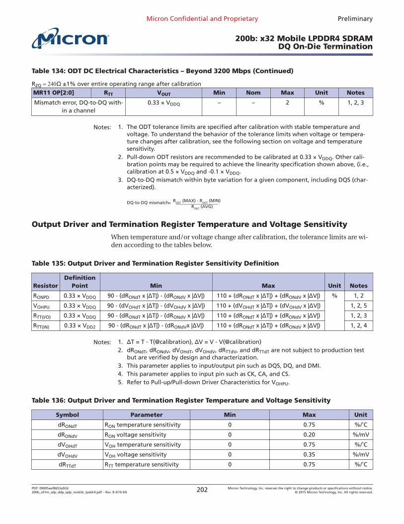
Table 134: ODT DC Electrical Characteristics – Beyond 3200 Mbps (Continued)
RZQ Ω ±1% over entire operating range after calibrationMR11 OP[2:0] RTT VOUT Min Nom Max Unit Notes
Mismatch error, DQ-to-DQ with-in a channel
0.33 × VDDQ – – 2 % 1, 2, 3
Notes: 1. The ODT tolerance limits are specified after calibration with stable temperature andvoltage. To understand the behavior of the tolerance limits when voltage or tempera-ture changes after calibration, see the following section on voltage and temperaturesensitivity.
2. Pull-down ODT resistors are recommended to be calibrated at 0.33 × VDDQ. Other cali-bration points may be required to achieve the linearity specification shown above, (i.e.,calibration at 0.5 × VDDQ and -0.1 × VDDQ.
3. DQ-to-DQ mismatch within byte variation for a given component, including DQS (char-acterized).
DQ-to-DQ mismatch = RODT (MAX) - RODT (MIN) RODT (AVG)
Output Driver and Termination Register Temperature and Voltage Sensitivity
When temperature and/or voltage change after calibration, the tolerance limits are wi-den according to the tables below.
Table 135: Output Driver and Termination Register Sensitivity Definition
ResistorDefinition
Point Min Max Unit Notes
RONPD 0.33 × VDDQ 90 - (dRONdT x |ΔT|) - (dRONdV x |ΔV|) 110 + (dRONdT x |ΔT|) + (dRONdV x |ΔV|) % 1, 2
VOHPU 0.33 × VDDQ 90 - (dVOHdT x |ΔT|) - (dVOHdV x |ΔV|) 110 + (dVOHdT x |ΔT|) + (dVOHdV x |ΔV|) 1, 2, 5
RTT(I/O) 0.33 × VDDQ 90 - (dRONdT x |ΔT|) - (dRONdV x |ΔV|) 110 + (dRONdT x |ΔT|) + (dRONdV x |ΔV|) 1, 2, 3
RTT(IN) 0.33 × VDD2 90 - (dRONdT x |ΔT|) - (dRONdVx |ΔV|) 110 + (dRONdT x |ΔT|) + (dRONdV x |ΔV|) 1, 2, 4
Notes: 1. ΔT = T - T(@calibration), ΔV = V - V(@calibration)2. dRONdT, dRONdV, dVOHdT, dVOHdV, dRTTdV, and dRTTdT are not subject to production test
but are verified by design and characterization.3. This parameter applies to input/output pin such as DQS, DQ, and DMI.4. This parameter applies to input pin such as CK, CA, and CS.5. Refer to Pull-up/Pull-down Driver Characteristics for VOHPU.
Table 136: Output Driver and Termination Register Temperature and Voltage Sensitivity
Symbol Parameter Min Max Unit
dRONdT RON temperature sensitivity 0 0.75 %/˚C
dRONdV RON voltage sensitivity 0 0.20 %/mV
dVOHdT VOH temperature sensitivity 0 0.75 %/˚C
dVOHdV VOH voltage sensitivity 0 0.35 %/mV
dRTTdT RTT temperature sensitivity 0 0.75 %/˚C
Micron Confidential and Proprietary Preliminary
200b: x32 Mobile LPDDR4 SDRAMDQ On-Die Termination
PDF: 09005aef8653a92d200b_z01m_sdp_ddp_qdp_mobile_lpddr4.pdf – Rev. B 4/16 EN 202 Micron Technology, Inc. reserves the right to change products or specifications without notice.
© 2015 Micron Technology, Inc. All rights reserved.
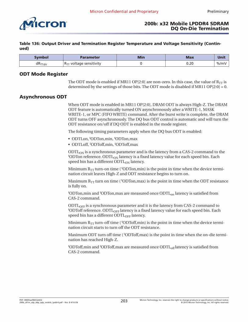
Table 136: Output Driver and Termination Register Temperature and Voltage Sensitivity (Contin-ued)
Symbol Parameter Min Max Unit
dRTTdV RTT voltage sensitivity 0 0.20 %/mV
ODT Mode Register
The ODT mode is enabled if MR11 OP[2:0] are non-zero. In this case, the value of RTT isdetermined by the settings of those bits. The ODT mode is disabled if MR11 OP[2:0] = 0.
Asynchronous ODT
When ODT mode is enabled in MR11 OP[2:0], DRAM ODT is always High-Z. The DRAMODT feature is automatically turned ON asynchronously after a WRITE-1, MASKWRITE-1, or MPC (FIFO WRITE) command. After the burst write is complete, the DRAMODT turns OFF asynchronously. The DQ bus ODT control is automatic and will turn theODT resistance on/off if DQ ODT is enabled in the mode register.
The following timing parameters apply when the DQ bus ODT is enabled:
• ODTLon, tODTon,min, tODTon,max• ODTLoff, tODToff,min, tODToff,max
ODTLON is a synchronous parameter and is the latency from a CAS-2 command to thetODTon reference. ODTLON latency is a fixed latency value for each speed bin. Eachspeed bin has a different ODTLON latency.
Minimum RTT turn-on time ( tODTon,min) is the point in time when the device termi-nation circuit leaves High-Z and ODT resistance begins to turn on.
Maximum RTT turn on time ( tODTon,max) is the point in time when the ODT resistanceis fully on.
tODTon,min and tODTon,max are measured once ODTLon latency is satisfied fromCAS-2 command.
ODTLOFF is a synchronous parameter and it is the latency from CAS-2 command totODToff reference. ODTLOFF latency is a fixed latency value for each speed bin. Eachspeed bin has a different ODTLOFF latency.
Minimum RTT turn-off time ( tODToff,min) is the point in time when the device termi-nation circuit starts to turn off the ODT resistance.
Maximum ODT turn off time ( tODToff,max) is the point in time when the on-die termi-nation has reached High-Z.
tODToff,min and tODToff,max are measured once ODTLoff latency is satisfied fromCAS-2 command.
Micron Confidential and Proprietary Preliminary
200b: x32 Mobile LPDDR4 SDRAMDQ On-Die Termination
PDF: 09005aef8653a92d200b_z01m_sdp_ddp_qdp_mobile_lpddr4.pdf – Rev. B 4/16 EN 203 Micron Technology, Inc. reserves the right to change products or specifications without notice.
© 2015 Micron Technology, Inc. All rights reserved.
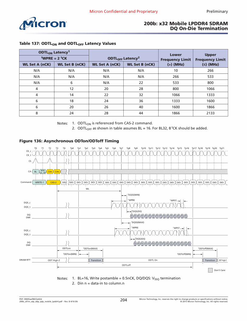
Table 137: ODTLON and ODTLOFF Latency Values
ODTLON Latency1
ODTLOFF Latency2Lower
Frequency Limit(>) (MHz)
UpperFrequency Limit
(≤≤) (MHz)
tWPRE = 2 tCK
WL Set A (nCK) WL Set B (nCK) WL Set A (nCK) WL Set B (nCK)
N/A N/A N/A N/A 10 266
N/A N/A N/A N/A 266 533
N/A 6 N/A 22 533 800
4 12 20 28 800 1066
4 14 22 32 1066 1333
6 18 24 36 1333 1600
6 20 26 40 1600 1866
8 24 28 44 1866 2133
Notes: 1. ODTLON is referenced from CAS-2 command.2. ODTLOFF as shown in table assumes BL = 16. For BL32, 8 tCK should be added.
Figure 136: Asynchronous ODTon/ODToff Timing
T0
CK_t
CK_cT1 T2 T3 T4 Ta12Ta9 Ta13Ta10Ta0 Ta1 Ta2 Ta3 Ta6 Ta7 Ta8 Ta17Ta11
CS
Ta5Ta4
CA BL
Command WRITE-1
BA0,CA, AP CAn
CAS-2
CAn
WL
DES DES DES DESDES DESDES DESDES DES DES DES DES DES DES
t WPRE
tDQSS(MIN)
DQS_t
DQS_c
DQDMI
DQDMI
Don’t Care
tDQS2DQ
Ta14 Ta19Ta15 Ta16 Ta18 Ta21Ta20
DES DES DES DES DES DES
Dinn0
Dinn1
Dinn2
Dinn13
Dinn14
Dinn15
DES DES
t WPST
Dinn3
Dinn4
Dinn5
Dinn6
Dinn7
Dinn8
Dinn9
Dinn10
Dinn11
Dinn12
t WPRE
tDQSS(MAX)
tODTon(MAX)
tODTon(MIN)
DQS_t
DQS_c
DRAM RTT
tDQS2DQ
ODT High-Z Transition ODT High-ZTransition
ODTLon
ODTLoff
ODTL On
Dinn0
Dinn1
Dinn2
Dinn13
Dinn14
Dinn15
t WPST
Dinn3
Dinn4
Dinn5
Dinn6
Dinn7
Dinn8
Dinn9
Dinn10
Dinn11
Dinn12
tODToff(MAX)
tODToff(MIN)
Notes: 1. BL=16, Write postamble = 0.5nCK, DQ/DQS: VSSQ termination2. Din n = data-in to column.n
Micron Confidential and Proprietary Preliminary
200b: x32 Mobile LPDDR4 SDRAMDQ On-Die Termination
PDF: 09005aef8653a92d200b_z01m_sdp_ddp_qdp_mobile_lpddr4.pdf – Rev. B 4/16 EN 204 Micron Technology, Inc. reserves the right to change products or specifications without notice.
© 2015 Micron Technology, Inc. All rights reserved.
3. DES commands are shown for ease of illustration; other commands may be valid atthese times.
DQ ODT During Power-Down and Self Refresh Modes
DQ bus ODT will be disabled in power-down mode. In self refresh mode, the ODT willbe turned off when CKE is LOW but will be enabled if CKE is HIGH and DQ ODT is ena-bled in the mode register.
ODT During Write Leveling Mode
If ODT is enabled in MR11 OP[2:0] in write leveling mode, the device always providesthe termination on DQS signals. DQ termination is always off in write leveling mode.
Table 138: Termination State in Write Leveling Mode
ODT State in MR11 OP[2:0] DQS TerminationDQ[15:0]/DMI[1:0]
Termination
Disabled Off Off
Enabled On Off
Micron Confidential and Proprietary Preliminary
200b: x32 Mobile LPDDR4 SDRAMDQ On-Die Termination
PDF: 09005aef8653a92d200b_z01m_sdp_ddp_qdp_mobile_lpddr4.pdf – Rev. B 4/16 EN 205 Micron Technology, Inc. reserves the right to change products or specifications without notice.
© 2015 Micron Technology, Inc. All rights reserved.
TRR Mode – Target Row RefreshThe device limits the number of times that a given row can be accessed within a refreshperiod (tREFW x 2) prior to requiring adjacent rows to be refreshed. The maximum acti-vate count (MAC) is the maximum number of activates that a single row can sustainwithin a refresh period before the adjacent rows need to be refreshed. The row receivingthe excessive actives is the target row (TRn), the adjacent rows to be refreshed are thevictim rows. When the MAC limit is reached on TRn, either the device receives all (R x 2)REFRESH commands before another row activate is issued, or the device should beplaced into targeted row refresh (TRR) mode. The TRR mode will refresh the rows adja-cent to the TRn that encountered tMAC limit.
If the device supports unlimited MAC value: MR24 OP[2:0] = 000 and MR24 OP[3] = 1,TARGET ROW REFRESH operation is not required. Even though the device allows to setMR24 OP[7] = 1: TRR mode enable, in this case the device behavior is vendor specific.For example, a certain device may ignore MRW command for entering/exiting TRRmode or a certain device may support commands related TRR mode. See vendor devicedatasheets for details about TRR mode definition at supporting unlimited MAC valuecase.
There could be a maximum of two target rows to a victim row in a bank. The cumulativevalue of the activates from the two target rows on a victim row in a bank should not ex-ceed MAC value.
MR24 fields are required to support the new TRR settings. Setting MR24 OP[7] = 1 ena-bles TRR mode and setting MR24 OP[7] = 0 disables TRR mode. MR24 OP[6:4] defineswhich bank (BAn) the target row is located in (refer to MR24 table for details).
The TRR mode must be disabled during initialization as well as any other device cali-bration modes. The TRR mode is entered from a DRAM idle state, once TRR mode hasbeen entered, no other mode register commands are allowed until TRR mode is com-pleted; however, setting MR24 OP[7] = 0 to interrupt and reissue the TRR mode is al-lowed.
When enabled, TRR mode is self-clearing. the mode will be disabled automatically afterthe completion of defined TRR flow (after the third BAn precharge has completed plustMRD). Optionally, the TRR mode can also be exited via another MRS command at thecompletion of TRR by setting MR24 OP[7] = 0. If the TRR is exited via another MRS com-mand, the value written to MR24 OP[6:4] are "Don’t Care".
TRR Mode Operation
1. The timing diagram depicts TRR mode. The following steps must be performedwhen TRR mode is enabled. This mode requires all three ACT (ACT1, ACT2, andACT3) and three corresponding PRE commands (PRE1, PRE2, and PRE3) to com-plete TRR mode. PRECHARGE All (PREA) commands issued while the device is inTRR mode will also perform precharge to BAn and counts towards PREn com-mand.
2. Prior to issuing the MRW command to enter TRR mode, the device should be inthe idle state. MRW command must be issued with MR24 OP[7] = 1 and MR24OP[6:4] defining the bank in which the targeted row is located. All other MR24 bitsshould remain unchanged.
3. No activity is to occur with the device until tMRD has been satisfied. Once tMRDhas been satisfied, the only commands allowed BAn, until TRR mode has comple-ted, are ACT and PRE.
Micron Confidential and Proprietary Preliminary
200b: x32 Mobile LPDDR4 SDRAMTRR Mode – Target Row Refresh
PDF: 09005aef8653a92d200b_z01m_sdp_ddp_qdp_mobile_lpddr4.pdf – Rev. B 4/16 EN 206 Micron Technology, Inc. reserves the right to change products or specifications without notice.
© 2015 Micron Technology, Inc. All rights reserved.
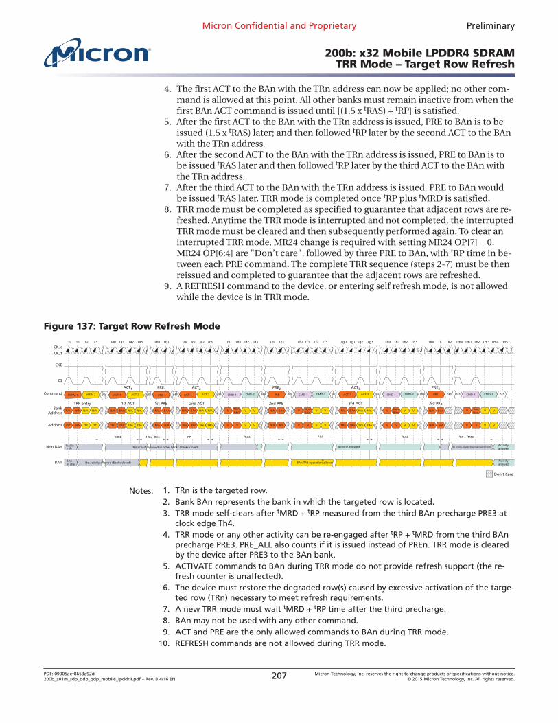
4. The first ACT to the BAn with the TRn address can now be applied; no other com-mand is allowed at this point. All other banks must remain inactive from when thefirst BAn ACT command is issued until [(1.5 x tRAS) + tRP] is satisfied.
5. After the first ACT to the BAn with the TRn address is issued, PRE to BAn is to beissued (1.5 x tRAS) later; and then followed tRP later by the second ACT to the BAnwith the TRn address.
6. After the second ACT to the BAn with the TRn address is issued, PRE to BAn is tobe issued tRAS later and then followed tRP later by the third ACT to the BAn withthe TRn address.
7. After the third ACT to the BAn with the TRn address is issued, PRE to BAn wouldbe issued tRAS later. TRR mode is completed once tRP plus tMRD is satisfied.
8. TRR mode must be completed as specified to guarantee that adjacent rows are re-freshed. Anytime the TRR mode is interrupted and not completed, the interruptedTRR mode must be cleared and then subsequently performed again. To clear aninterrupted TRR mode, MR24 change is required with setting MR24 OP[7] = 0,MR24 OP[6:4] are "Don’t care", followed by three PRE to BAn, with tRP time in be-tween each PRE command. The complete TRR sequence (steps 2-7) must be thenreissued and completed to guarantee that the adjacent rows are refreshed.
9. A REFRESH command to the device, or entering self refresh mode, is not allowedwhile the device is in TRR mode.
Figure 137: Target Row Refresh ModeT0 T1 Ta0 Ta1T3T2 Ta2 Ta3 Tc0 Tc1 Tc2 Tc3 Td0 Td1 Td2 Td3 Tf0 Tf1 Tf2 Tf3 Tg0 Tg1 Tg2 Tg3 Th0 Th1 Th2 Th3 Tm0 Tm1 Tm2 Tm3 Tm4 Tm5Tk0 Tk1 Tk2Tb0 Tb1
CK_c
CK_t
Te0 Te1
CS
BankAddress
Address
Command
CKE
Don’t Care
Non BAn
MRW-1 MRW-2 DES ACT-1 ACT-2 DES PRE DES PRE DES PRE DES DESACT-1 ACT-2 DES CMD-1 CMD-2 DES CMD-1 CMD-2 DES ACT-1 ACT-2 DES CMD-1 CMD-2 DES CMD-1 CMD-2 DES
PRE3
3rd PRE3rd ACT2nd PRE2nd ACT1st PRE
PRE2PRE1 ACT3ACT2
N/A N/A N/AN/A
OP OP OPMA
N/A N/A N/ABAn
TRn TRn TRnTRn
N/A BAn
N/A N/A
N/A N/A N/ABAn
TRn TRn TRnTRn
V V VNonBAn
V V VV
N/A BAn
N/A N/A
N/A N/A N/ABAn
TRn TRn TRnTRn
V V VNonBAn
V V VV
N/A BAn
N/A N/A
V V VNonBAn
V V VV
V V VAnyBAn
V V VV
1st ACT
ACT1
TRR entry
Non BAnin idle
Activityallowed
BAn BAnin idle No activity allowed (Banks closed)
ActivityallowedBAn TRR operation allowed
tMRD tRP t
9
tRAS tRAS RP tRAS1.5 x tMRDtRP +
No activity allowed in other banks (Banks closed) Activity allowed No activity allowed (may have bank(s) open)
Notes: 1. TRn is the targeted row.2. Bank BAn represents the bank in which the targeted row is located.3. TRR mode self-clears after tMRD + tRP measured from the third BAn precharge PRE3 at
clock edge Th4.4. TRR mode or any other activity can be re-engaged after tRP + tMRD from the third BAn
precharge PRE3. PRE_ALL also counts if it is issued instead of PREn. TRR mode is clearedby the device after PRE3 to the BAn bank.
5. ACTIVATE commands to BAn during TRR mode do not provide refresh support (the re-fresh counter is unaffected).
6. The device must restore the degraded row(s) caused by excessive activation of the targe-ted row (TRn) necessary to meet refresh requirements.
7. A new TRR mode must wait tMRD + tRP time after the third precharge.8. BAn may not be used with any other command.9. ACT and PRE are the only allowed commands to BAn during TRR mode.
10. REFRESH commands are not allowed during TRR mode.
Micron Confidential and Proprietary Preliminary
200b: x32 Mobile LPDDR4 SDRAMTRR Mode – Target Row Refresh
PDF: 09005aef8653a92d200b_z01m_sdp_ddp_qdp_mobile_lpddr4.pdf – Rev. B 4/16 EN 207 Micron Technology, Inc. reserves the right to change products or specifications without notice.
© 2015 Micron Technology, Inc. All rights reserved.
11. All timings are to be met by DRAM during TRR mode, such as tFAW. Issuing ACT1, ACT2,and ACT3 counts towards tFAW budget.
Post-Package RepairThe device has fail row address repair as an optional post-package repair (PPR) featureand it is readable through MR25 OP[7:0].
PPR provides simple and easy repair method in the system and fail row address can berepaired by the electrical programming of Electrical-fuse scheme. The device can cor-rect one row per bank with PPR.
Electrical-fuse cannot be switched back to un-fused states once it is programmed. Thecontroller should prevent unintended PPR mode entry and repair.
Failed Row Address Repair
1. Before entering PPR mode, all banks must be precharged.2. Enable PPR using MR4 OP[4] = 1 and wait tMRD.3. Issue ACT command with fail row address.4. Wait tPGM to allow the device repair target row address internally then issue PRE-
CHARGE5. Wait tPGM_EXIT after PRECHARGE, which allows the device to recognize repaired
row address RAn.6. Exit PPR mode with setting MR4 OP[4] = 0.7. The device is ready for any valid command after tPGMPST.8. In more than one fail address repair case, repeat step 2 to 7.
Once PPR mode is exited, to confirm whether the target row has correctly repaired, thehost can verify the repair by writing data into the target row and reading it back afterPPR exit with MR4 OP[4] = 0 and tPGMPST.
The following timing diagram shows PPR operation.
Micron Confidential and Proprietary Preliminary
200b: x32 Mobile LPDDR4 SDRAMPost-Package Repair
PDF: 09005aef8653a92d200b_z01m_sdp_ddp_qdp_mobile_lpddr4.pdf – Rev. B 4/16 EN 208 Micron Technology, Inc. reserves the right to change products or specifications without notice.
© 2015 Micron Technology, Inc. All rights reserved.
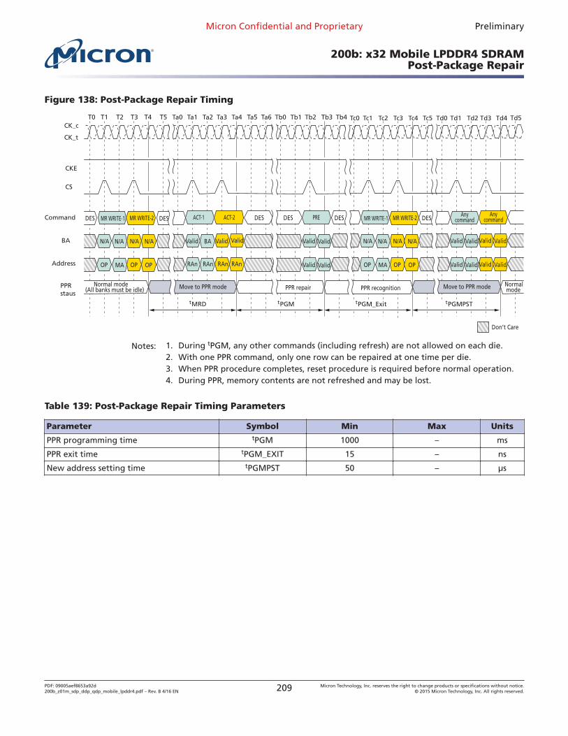
Figure 138: Post-Package Repair Timing
T0
CK_t
CK_cT1 T2 T3
PPRstaus
T4
Command
Address
CS
CKE
Ta5 Ta6
Don’t Care
T5 Tb0Ta3 Tb1 Tb4Tb2Ta0 Ta1 Ta2 Ta4 Tc5Tc3Tc0 Tc1 Tc2 Tc4 Td3Td0 Td1 Td2 Td4 Td5Tb3
DES MR WRITE-1 MR WRITE-2 DES DESDES DESDES
BA N/A N/A
OP MA
ACT-1
Valid BA
RAn RAn
PRE
ValidN/A N/A
OP OP
MR WRITE-1 MR WRITE-2
N/A N/A
OP MA
N/A N/A
OP OP
ACT-2
Valid Valid Valid
Valid Valid
Anycommand
Valid Valid
Valid Valid
Anycommand
Valid Valid
Valid ValidRAn RAn
Normal mode Normal(All banks must be idle) Move to PPR mode Move to PPR modePPR repair PPR recognition mode
tMRD tPGM tPGM_Exit tPGMPST
Notes: 1. During tPGM, any other commands (including refresh) are not allowed on each die.2. With one PPR command, only one row can be repaired at one time per die.3. When PPR procedure completes, reset procedure is required before normal operation.4. During PPR, memory contents are not refreshed and may be lost.
Table 139: Post-Package Repair Timing Parameters
Parameter Symbol Min Max Units
PPR programming time tPGM 1000 – ms
PPR exit time tPGM_EXIT 15 – ns
New address setting time tPGMPST 50 – μs
Micron Confidential and Proprietary Preliminary
200b: x32 Mobile LPDDR4 SDRAMPost-Package Repair
PDF: 09005aef8653a92d200b_z01m_sdp_ddp_qdp_mobile_lpddr4.pdf – Rev. B 4/16 EN 209 Micron Technology, Inc. reserves the right to change products or specifications without notice.
© 2015 Micron Technology, Inc. All rights reserved.
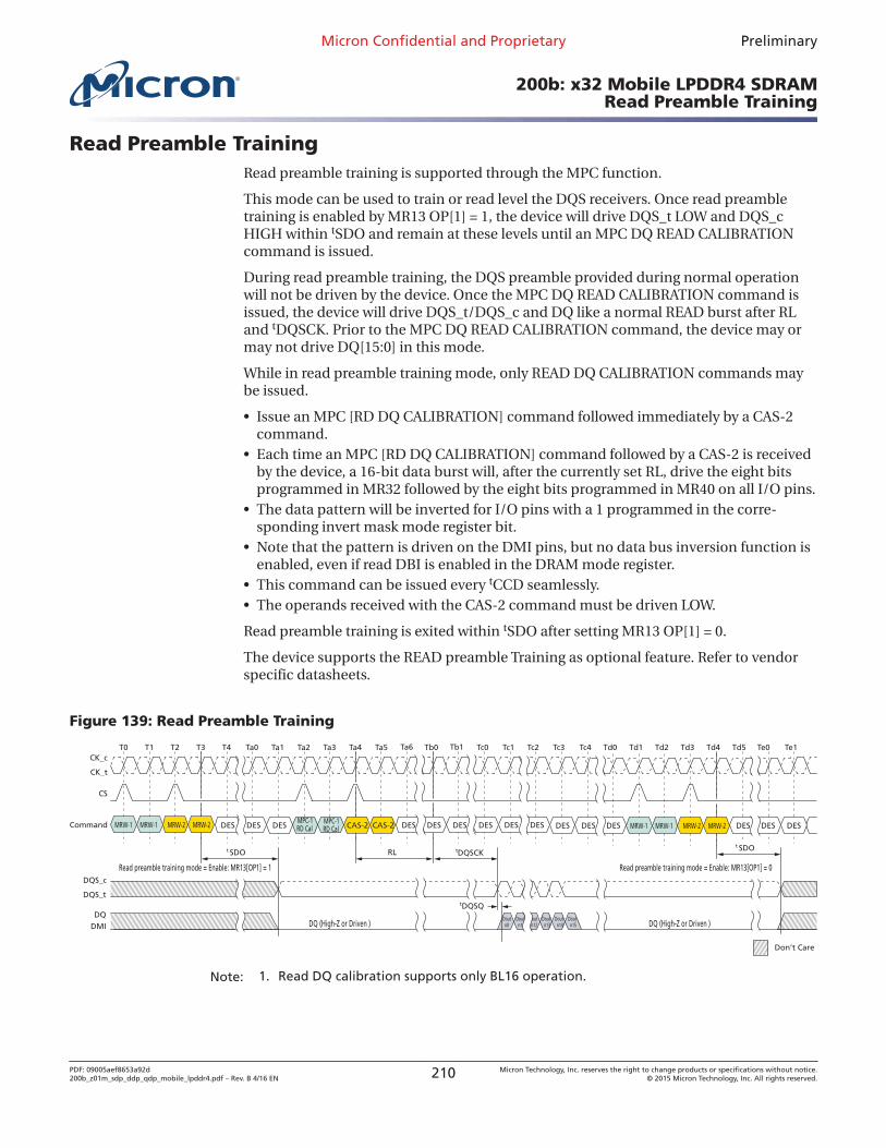
Read Preamble TrainingRead preamble training is supported through the MPC function.
This mode can be used to train or read level the DQS receivers. Once read preambletraining is enabled by MR13 OP[1] = 1, the device will drive DQS_t LOW and DQS_cHIGH within tSDO and remain at these levels until an MPC DQ READ CALIBRATIONcommand is issued.
During read preamble training, the DQS preamble provided during normal operationwill not be driven by the device. Once the MPC DQ READ CALIBRATION command isissued, the device will drive DQS_t/DQS_c and DQ like a normal READ burst after RLand tDQSCK. Prior to the MPC DQ READ CALIBRATION command, the device may ormay not drive DQ[15:0] in this mode.
While in read preamble training mode, only READ DQ CALIBRATION commands maybe issued.
• Issue an MPC [RD DQ CALIBRATION] command followed immediately by a CAS-2command.
• Each time an MPC [RD DQ CALIBRATION] command followed by a CAS-2 is receivedby the device, a 16-bit data burst will, after the currently set RL, drive the eight bitsprogrammed in MR32 followed by the eight bits programmed in MR40 on all I/O pins.
• The data pattern will be inverted for I/O pins with a 1 programmed in the corre-sponding invert mask mode register bit.
• Note that the pattern is driven on the DMI pins, but no data bus inversion function isenabled, even if read DBI is enabled in the DRAM mode register.
• This command can be issued every tCCD seamlessly.• The operands received with the CAS-2 command must be driven LOW.
Read preamble training is exited within tSDO after setting MR13 OP[1] = 0.
The device supports the READ preamble Training as optional feature. Refer to vendorspecific datasheets.
Figure 139: Read Preamble Training
T0
CK_t
CK_cT1 T2 T3 T4 Ta0 Tc1Ta1 Tb0 Tb1Ta2 Ta3 Ta4 Ta5 Ta6 Td2 Td3 Td4 Td5Tc0 Tc3 Tc4Tc2
CS
Td1Td0 Te1Te0
Command CAS-2 CAS-2
RL
DES DES DES DES DES DES DES DES DES DESDES DES
tDQSCK
tDQSQDQS_t
DQS_c
DQDMI
Don’t Care
MPC-1RD Cal
MPC-1RD Cal
SDOt SDOt
Doutn0
Doutn1
Doutn13
Doutn12
Doutn14
Doutn15
DES DESDESMRW-1 MRW-1 MRW-2 MRW-2 MRW-1 MRW-1 MRW-2 MRW-2
Read preamble training mode = Enable: MR13[OP1] = 1 Read preamble training mode = Enable: MR13[OP1] = 0
DQ (High-Z or Driven ) DQ (High-Z or Driven )
Note: 1. Read DQ calibration supports only BL16 operation.
Micron Confidential and Proprietary Preliminary
200b: x32 Mobile LPDDR4 SDRAMRead Preamble Training
PDF: 09005aef8653a92d200b_z01m_sdp_ddp_qdp_mobile_lpddr4.pdf – Rev. B 4/16 EN 210 Micron Technology, Inc. reserves the right to change products or specifications without notice.
© 2015 Micron Technology, Inc. All rights reserved.
Electrical Specifications
Absolute Maximum Ratings
Stresses greater than those listed in the table below may cause permanent damage tothe device. This is a stress rating only, and functional operation of the device at theseconditions, or any other conditions outside those indicated in the operational sectionsof this document, is not implied. Exposure to absolute maximum rating conditions forextended periods may adversely affect reliability.
Table 140: Absolute Maximum DC Ratings
Parameter Symbol Min Max Unit Notes
VDD1 supply voltage relative to VSS VDD1 –0.4 2.1 V 1
VDD2 supply voltage relative to VSS VDD2 –0.4 1.5 V 1
VDDQ supply voltage relative to VSS VDDQ –0.4 1.5 V 1
Voltage on any ball relative to VSS VIN, VOUT –0.4 1.5 V
Storage temperature TSTG –55 125 ˚C 2
Notes: 1. For information about relationships between power supplies, see the Voltage Ramp andDevice Initialization section.
2. Storage temperature is the case surface temperature on the center/top side of the de-vice. For measurement conditions, refer to the JESD51-2 standard.
AC and DC Operating ConditionsOperation or timing that is not specified is illegal. To ensure proper operation, the de-vice must be initialized properly.
Table 141: Recommended DC Operating Conditions
Symbol Min Typ Max DRAM Unit Notes
VDD1 1.7 1.8 1.95 Core 1 power V 1, 2
VDD2 1.06 1.1 1.17 Core 2 power/Input bufferpower
V 1, 2, 3
VDDQ 1.06 1.1 1.17 I/O buffer power V 2, 3
Notes: 1. VDD1 uses significantly less power than VDD2.2. The voltage range is for DC voltage only. DC voltage is the voltage supplied at the
DRAM and is inclusive of all noise up to 20 MHz at the DRAM package ball.3. The voltage noise tolerance from DC to 20 MHz exceeding a peak-to-peak tolerance of
45mV at the DRAM ball is not included in the TdIVW.
Micron Confidential and Proprietary Preliminary
200b: x32 Mobile LPDDR4 SDRAMElectrical Specifications
PDF: 09005aef8653a92d200b_z01m_sdp_ddp_qdp_mobile_lpddr4.pdf – Rev. B 4/16 EN 211 Micron Technology, Inc. reserves the right to change products or specifications without notice.
© 2015 Micron Technology, Inc. All rights reserved.
Table 142: Input Leakage Current
Parameter/Condition Symbol Min Max Unit Notes
Input leakage current IL –2 2 μA 1, 2
Notes: 1. For CK_t, CK_c, CKE, CS, CA, ODT_CA and RESET_n. Any input 0V ≤ VIN ≤ VDD2. (All otherpins not under test = 0V.
2. CA ODT is disabled for CK_t, CK_c, CS, and CA.
Table 143: Input/Output Leakage Current
Parameter/Condition Symbol Min Max Unit Notes
Input/Output leakage current IOZ –5 5 μA 1, 2
Notes: 1. For DQ, DQS_t, DQS_c and DMI. Any I/O 0V ≤ VOUT ≤ VDDQ.2. I/Os status are disabled: High Impedance and ODT off.
Table 144: Operating Temperature Range
Parameter/Condition Symbol Min Max Unit
Standard TOPER –30 85 ˚C
Elevated 85 105 ˚C
Notes: 1. Operating temperature is the case surface temperature at the center of the top side ofthe device. For measurement conditions, refer to the JESD51-2 standard.
2. When using the device in the elevated temperature range, some derating may be re-quired. See Mode Registers for vendor-specific derating.
3. Either the device case temperature rating or the temperature sensor can be used to setan appropriate refresh rate, determine the need for AC timing derating, and/or monitorthe operating temperature (see Temperature Sensor). When using the temperature sen-sor, the actual device case temperature may be higher than the TOPER rating that appliesfor the standard or elevated temperature range. For example, TCASE could be above+85˚C when the temperature sensor indicates a temperature of less than +85˚C.
Micron Confidential and Proprietary Preliminary
200b: x32 Mobile LPDDR4 SDRAMAC and DC Operating Conditions
PDF: 09005aef8653a92d200b_z01m_sdp_ddp_qdp_mobile_lpddr4.pdf – Rev. B 4/16 EN 212 Micron Technology, Inc. reserves the right to change products or specifications without notice.
© 2015 Micron Technology, Inc. All rights reserved.
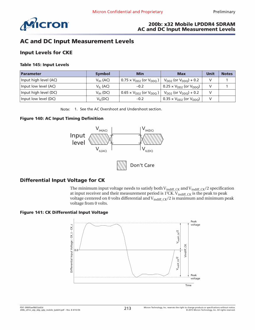
AC and DC Input Measurement Levels
Input Levels for CKE
Table 145: Input Levels
Parameter Symbol Min Max Unit Notes
Input high level (AC) VIH (AC) 0.75 × VDD2 (or VDDQ ) VDD2 (or VDDQ) + 0.2 V 1
Input low level (AC) VIL (AC) –0.2 0.25 × VDD2 (or VDDQ) V 1
Input high level (DC) VIH (DC) 0.65 × VDD2 (or VDDQ ) VDD2 (or VDDQ) + 0.2 V
Input low level (DC) VIL(DC) –0.2 0.35 × VDD2 (or VDDQ) V
Note: 1. See the AC Overshoot and Undershoot section.
Figure 140: AC Input Timing Definition
VIH(AC)
VIL(AC)
VIH(DC)
VIL(DC)
Inputlevel
Don’t Care
Differential Input Voltage for CK
The minimum input voltage needs to satisfy both Vindiff_CK and Vindiff_CK/2 specificationat input receiver and their measurement period is 1tCK. Vindiff_CK is the peak to peakvoltage centered on 0 volts differential and Vindiff_CK/2 is maximum and minimum peakvoltage from 0 volts.
Figure 141: CK Differential Input Voltage
0.0
Dif
fere
nti
al In
pu
t V
olt
age
: CK
_t -
CK
_c
Vin
dif
f_C
K/2
Time
Peakvoltage
Peakvoltage
Vin
dif
f_C
K
Vin
dif
f_C
K/2
Micron Confidential and Proprietary Preliminary
200b: x32 Mobile LPDDR4 SDRAMAC and DC Input Measurement Levels
PDF: 09005aef8653a92d200b_z01m_sdp_ddp_qdp_mobile_lpddr4.pdf – Rev. B 4/16 EN 213 Micron Technology, Inc. reserves the right to change products or specifications without notice.
© 2015 Micron Technology, Inc. All rights reserved.
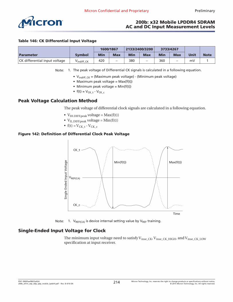
Table 146: CK Differential Input Voltage
Parameter Symbol
1600/1867 2133/2400/3200 3733/4267
Unit NoteMin Max Min Max Min Max
CK differential input voltage Vindiff_CK 420 – 380 – 360 – mV 1
Note: 1. The peak voltage of Differential CK signals is calculated in a following equation.
• Vindiff_CK = (Maximum peak voltage) - (Minimum peak voltage)• Maximum peak voltage = Max(f(t))• Minimum peak voltage = Min(f(t))• f(t) = VCK_t - VCK_c
Peak Voltage Calculation Method
The peak voltage of differential clock signals are calculated in a following equation.
• VIH.DIFF.peak voltage = Max(f(t))• VIL.DIFF.peak voltage = Min(f(t))• f(t) = VCK_t - VCK_c
Figure 142: Definition of Differential Clock Peak Voltage
Time
CK_t
VREF(CA)
Min(f(t)) Max(f(t))
CK_c
Sin
gle
En
ded
Inp
ut
Vo
ltag
e
Note: 1. VREF(CA) is device internal setting value by VREF training.
Single-Ended Input Voltage for Clock
The minimum input voltage need to satisfy Vinse_CK, Vinse_CK_HIGH, and Vinse_CK_LOWspecification at input receiver.
Micron Confidential and Proprietary Preliminary
200b: x32 Mobile LPDDR4 SDRAMAC and DC Input Measurement Levels
PDF: 09005aef8653a92d200b_z01m_sdp_ddp_qdp_mobile_lpddr4.pdf – Rev. B 4/16 EN 214 Micron Technology, Inc. reserves the right to change products or specifications without notice.
© 2015 Micron Technology, Inc. All rights reserved.
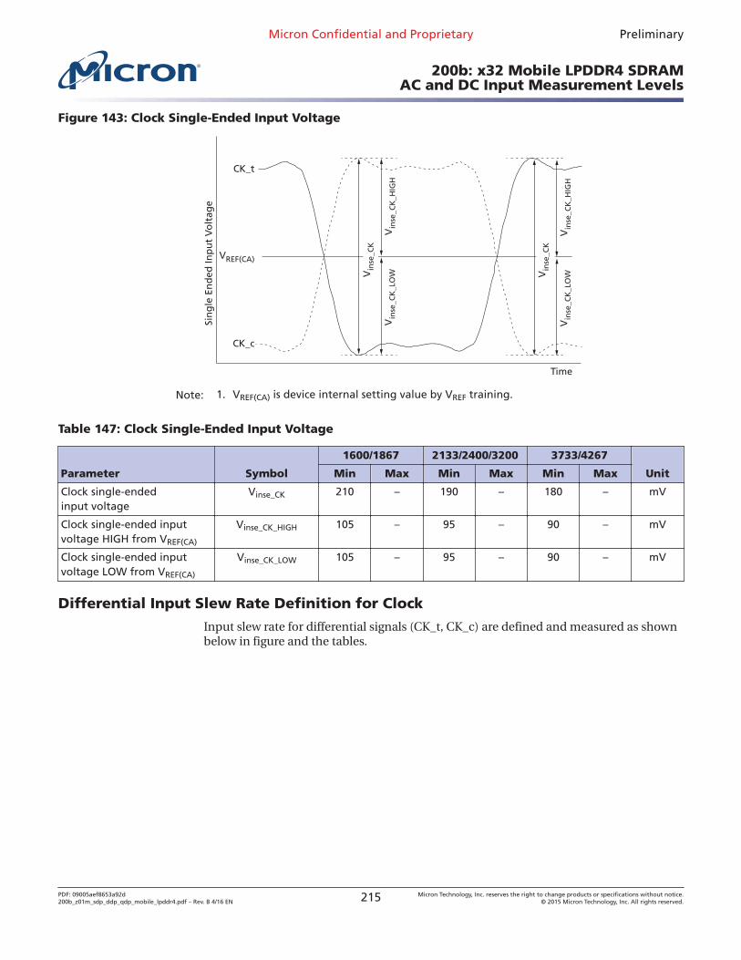
Figure 143: Clock Single-Ended Input Voltage
Time
CK_t
VREF(CA)
CK_c
Sin
gle
En
ded
Inp
ut
Vo
ltag
e
Vin
se_C
K
Vin
se_C
K_L
OW
Vin
se_C
K_H
IGH
Vin
se_C
K_L
OW
Vin
se_C
K_H
IGH
Vin
se_C
K
Note: 1. VREF(CA) is device internal setting value by VREF training.
Table 147: Clock Single-Ended Input Voltage
Parameter Symbol
1600/1867 2133/2400/3200 3733/4267
UnitMin Max Min Max Min Max
Clock single-endedinput voltage
Vinse_CK 210 – 190 – 180 – mV
Clock single-ended inputvoltage HIGH from VREF(CA)
Vinse_CK_HIGH 105 – 95 – 90 – mV
Clock single-ended inputvoltage LOW from VREF(CA)
Vinse_CK_LOW 105 – 95 – 90 – mV
Differential Input Slew Rate Definition for Clock
Input slew rate for differential signals (CK_t, CK_c) are defined and measured as shownbelow in figure and the tables.
Micron Confidential and Proprietary Preliminary
200b: x32 Mobile LPDDR4 SDRAMAC and DC Input Measurement Levels
PDF: 09005aef8653a92d200b_z01m_sdp_ddp_qdp_mobile_lpddr4.pdf – Rev. B 4/16 EN 215 Micron Technology, Inc. reserves the right to change products or specifications without notice.
© 2015 Micron Technology, Inc. All rights reserved.
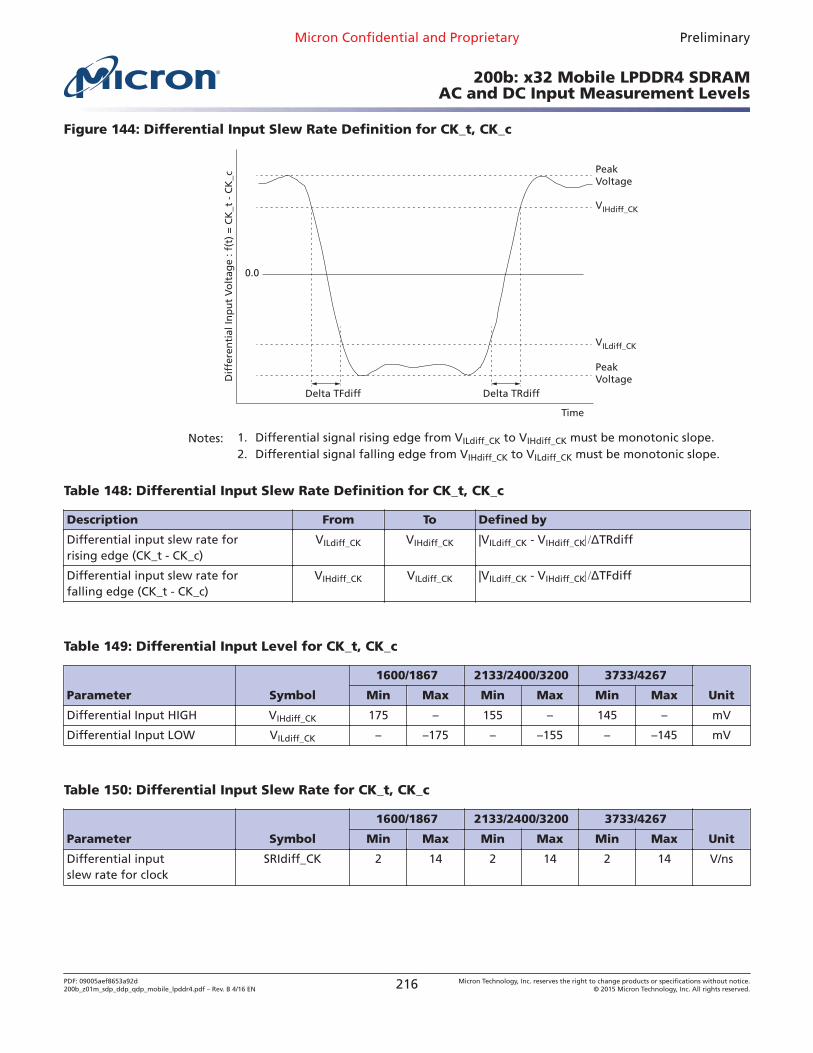
Figure 144: Differential Input Slew Rate Definition for CK_t, CK_c
Time
Dif
fere
nti
al In
pu
t V
olt
age
: f(t
) =
CK
_t -
CK
_c
PeakVoltage
PeakVoltage
VILdiff_CK
VIHdiff_CK
Delta TFdiff
0.0
Delta TRdiff
Notes: 1. Differential signal rising edge from VILdiff_CK to VIHdiff_CK must be monotonic slope.2. Differential signal falling edge from VIHdiff_CK to VILdiff_CK must be monotonic slope.
Table 148: Differential Input Slew Rate Definition for CK_t, CK_c
Description From To Defined by
Differential input slew rate forrising edge (CK_t - CK_c)
VILdiff_CK VIHdiff_CK |VILdiff_CK - VIHdiff_CKΔTRdiff
Differential input slew rate forfalling edge (CK_t - CK_c)
VIHdiff_CK VILdiff_CK |VILdiff_CK - VIHdiff_CKΔTFdiff
Table 149: Differential Input Level for CK_t, CK_c
Parameter Symbol
1600/1867 2133/2400/3200 3733/4267
UnitMin Max Min Max Min Max
Differential Input HIGH VIHdiff_CK 175 – 155 – 145 – mV
Differential Input LOW VILdiff_CK – –175 – –155 – –145 mV
Table 150: Differential Input Slew Rate for CK_t, CK_c
Parameter Symbol
1600/1867 2133/2400/3200 3733/4267
UnitMin Max Min Max Min Max
Differential inputslew rate for clock
SRIdiff_CK 2 14 2 14 2 14 V/ns
Micron Confidential and Proprietary Preliminary
200b: x32 Mobile LPDDR4 SDRAMAC and DC Input Measurement Levels
PDF: 09005aef8653a92d200b_z01m_sdp_ddp_qdp_mobile_lpddr4.pdf – Rev. B 4/16 EN 216 Micron Technology, Inc. reserves the right to change products or specifications without notice.
© 2015 Micron Technology, Inc. All rights reserved.
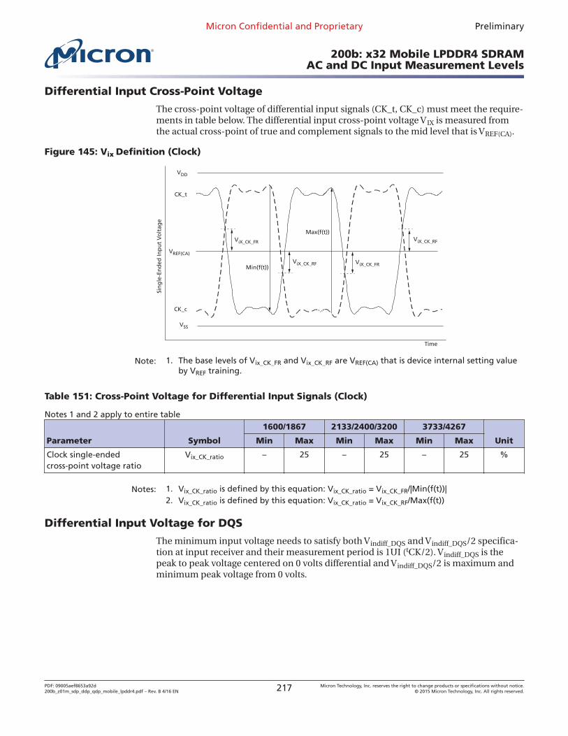
Differential Input Cross-Point Voltage
The cross-point voltage of differential input signals (CK_t, CK_c) must meet the require-ments in table below. The differential input cross-point voltage VIX is measured fromthe actual cross-point of true and complement signals to the mid level that is VREF(CA).
Figure 145: Vix Definition (Clock)Si
ng
le-E
nd
ed In
pu
t V
olt
age
Time
CK_t
VDD
ViX_CK_FR
ViX_CK_RFMin(f(t))
Max(f(t))
ViX_CK_FR
ViX_CK_RF
VSS
VREF(CA)
CK_c
Note: 1. The base levels of Vix_CK_FR and Vix_CK_RF are VREF(CA) that is device internal setting valueby VREF training.
Table 151: Cross-Point Voltage for Differential Input Signals (Clock)
Notes 1 and 2 apply to entire table
Parameter Symbol
1600/1867 2133/2400/3200 3733/4267
UnitMin Max Min Max Min Max
Clock single-endedcross-point voltage ratio
Vix_CK_ratio – 25 – 25 – 25 %
Notes: 1. Vix_CK_ratio is defined by this equation: Vix_CK_ratio = Vix_CK_FR/|Min(f(t))|2. Vix_CK_ratio is defined by this equation: Vix_CK_ratio = Vix_CK_RF/Max(f(t))
Differential Input Voltage for DQS
The minimum input voltage needs to satisfy both Vindiff_DQS and Vindiff_DQS/2 specifica-tion at input receiver and their measurement period is 1UI (tCK/2). Vindiff_DQS is thepeak to peak voltage centered on 0 volts differential and Vindiff_DQS/2 is maximum andminimum peak voltage from 0 volts.
Micron Confidential and Proprietary Preliminary
200b: x32 Mobile LPDDR4 SDRAMAC and DC Input Measurement Levels
PDF: 09005aef8653a92d200b_z01m_sdp_ddp_qdp_mobile_lpddr4.pdf – Rev. B 4/16 EN 217 Micron Technology, Inc. reserves the right to change products or specifications without notice.
© 2015 Micron Technology, Inc. All rights reserved.
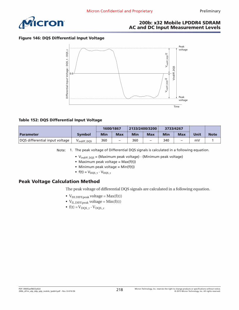
Figure 146: DQS Differential Input Voltage
0.0
Dif
fere
nti
al In
pu
t V
olt
age
: DQ
S_t
- D
QS_
c
Vin
dif
f_D
QS/2
Time
Peakvoltage
Peakvoltage
Vin
dif
f_D
QS
Vin
dif
f_D
QS/2
Table 152: DQS Differential Input Voltage
Parameter Symbol
1600/1867 2133/2400/3200 3733/4267
Unit NoteMin Max Min Max Min Max
DQS differential input voltage Vindiff_DQS 360 – 360 – 340 – mV 1
Note: 1. The peak voltage of Differential DQS signals is calculated in a following equation.
• Vindiff_DQS = (Maximum peak voltage) - (Minimum peak voltage)• Maximum peak voltage = Max(f(t))• Minimum peak voltage = Min(f(t))• f(t) = VDQS_t - VDQS_c
Peak Voltage Calculation Method
The peak voltage of differential DQS signals are calculated in a following equation.
• VIH.DIFF.peak voltage = Max(f(t))• VIL.DIFF.peak voltage = Min(f(t))• f(t) = VDQS_t - VDQS_c
Micron Confidential and Proprietary Preliminary
200b: x32 Mobile LPDDR4 SDRAMAC and DC Input Measurement Levels
PDF: 09005aef8653a92d200b_z01m_sdp_ddp_qdp_mobile_lpddr4.pdf – Rev. B 4/16 EN 218 Micron Technology, Inc. reserves the right to change products or specifications without notice.
© 2015 Micron Technology, Inc. All rights reserved.
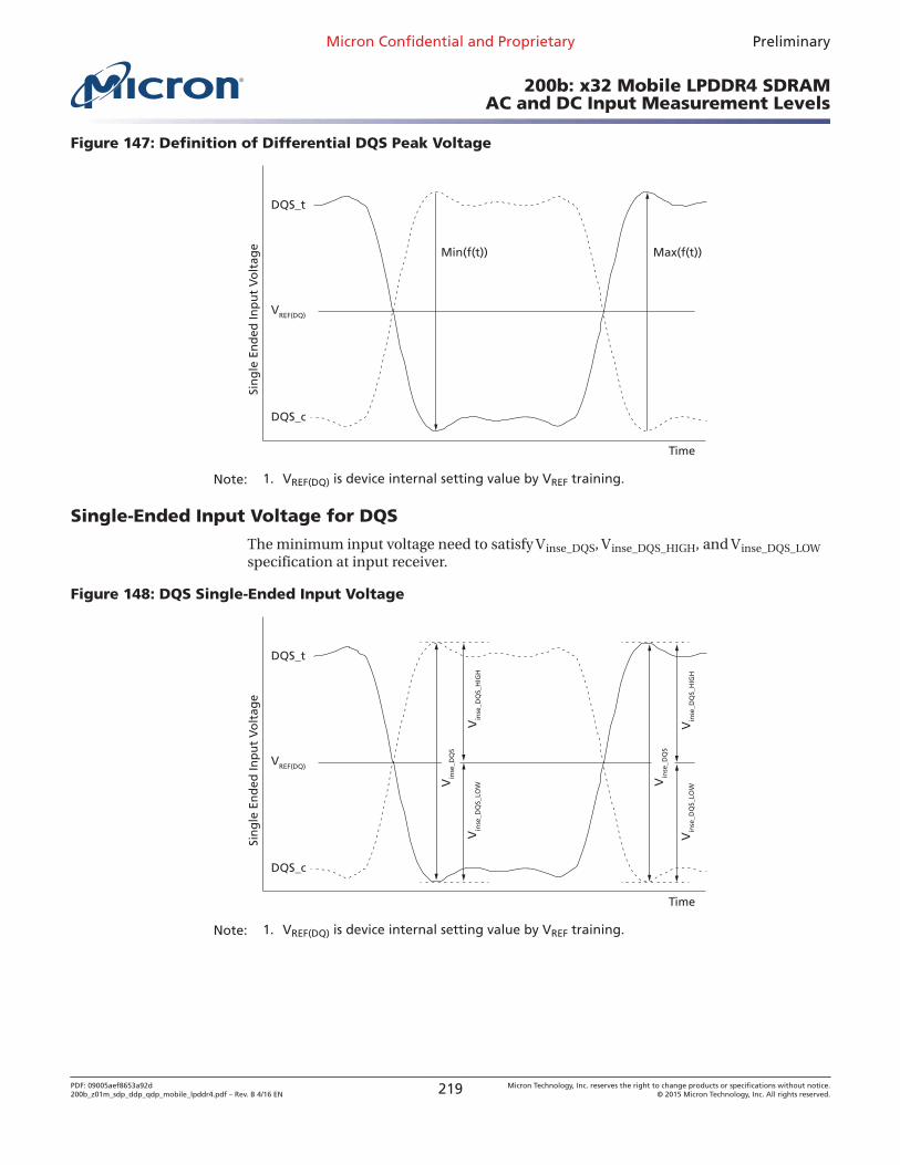
Figure 147: Definition of Differential DQS Peak Voltage
Time
DQS_t
VREF(DQ)
Min(f(t)) Max(f(t))
DQS_c
Sin
gle
En
ded
Inp
ut
Vo
ltag
e
Note: 1. VREF(DQ) is device internal setting value by VREF training.
Single-Ended Input Voltage for DQS
The minimum input voltage need to satisfy Vinse_DQS, Vinse_DQS_HIGH, and Vinse_DQS_LOWspecification at input receiver.
Figure 148: DQS Single-Ended Input Voltage
Time
DQS_t
VREF(DQ)
DQS_c
Sin
gle
En
ded
Inp
ut
Vo
ltag
e
Vin
se_D
QS
Vin
se_D
QS_
LOW
Vin
se_D
QS_
HIG
H
Vin
se_D
QS
Vin
se_D
QS_
LOW
Vin
se_D
QS_
HIG
H
Note: 1. VREF(DQ) is device internal setting value by VREF training.
Micron Confidential and Proprietary Preliminary
200b: x32 Mobile LPDDR4 SDRAMAC and DC Input Measurement Levels
PDF: 09005aef8653a92d200b_z01m_sdp_ddp_qdp_mobile_lpddr4.pdf – Rev. B 4/16 EN 219 Micron Technology, Inc. reserves the right to change products or specifications without notice.
© 2015 Micron Technology, Inc. All rights reserved.
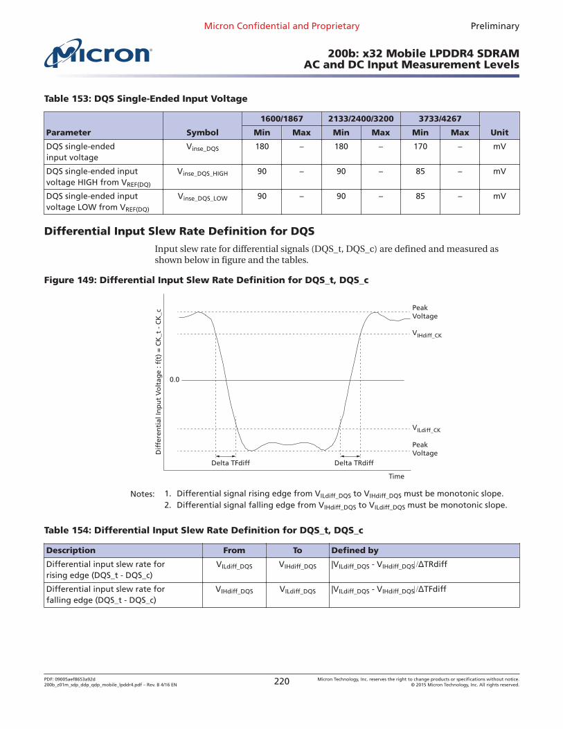
Table 153: DQS Single-Ended Input Voltage
Parameter Symbol
1600/1867 2133/2400/3200 3733/4267
UnitMin Max Min Max Min Max
DQS single-endedinput voltage
Vinse_DQS 180 – 180 – 170 – mV
DQS single-ended inputvoltage HIGH from VREF(DQ)
Vinse_DQS_HIGH 90 – 90 – 85 – mV
DQS single-ended inputvoltage LOW from VREF(DQ)
Vinse_DQS_LOW 90 – 90 – 85 – mV
Differential Input Slew Rate Definition for DQS
Input slew rate for differential signals (DQS_t, DQS_c) are defined and measured asshown below in figure and the tables.
Figure 149: Differential Input Slew Rate Definition for DQS_t, DQS_c
Time
Dif
fere
nti
al In
pu
t V
olt
age
: f(t
) =
CK
_t -
CK
_c
PeakVoltage
PeakVoltage
VILdiff_CK
VIHdiff_CK
Delta TFdiff
0.0
Delta TRdiff
Notes: 1. Differential signal rising edge from VILdiff_DQS to VIHdiff_DQS must be monotonic slope.2. Differential signal falling edge from VIHdiff_DQS to VILdiff_DQS must be monotonic slope.
Table 154: Differential Input Slew Rate Definition for DQS_t, DQS_c
Description From To Defined by
Differential input slew rate forrising edge (DQS_t - DQS_c)
VILdiff_DQS VIHdiff_DQS |VILdiff_DQS - VIHdiff_DQSΔTRdiff
Differential input slew rate forfalling edge (DQS_t - DQS_c)
VIHdiff_DQS VILdiff_DQS |VILdiff_DQS - VIHdiff_DQSΔTFdiff
Micron Confidential and Proprietary Preliminary
200b: x32 Mobile LPDDR4 SDRAMAC and DC Input Measurement Levels
PDF: 09005aef8653a92d200b_z01m_sdp_ddp_qdp_mobile_lpddr4.pdf – Rev. B 4/16 EN 220 Micron Technology, Inc. reserves the right to change products or specifications without notice.
© 2015 Micron Technology, Inc. All rights reserved.
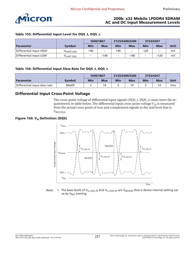
Table 155: Differential Input Level for DQS_t, DQS_c
Parameter Symbol
1600/1867 2133/2400/3200 3733/4267
UnitMin Max Min Max Min Max
Differential Input HIGH VIHdiff_DQS 140 – 140 – 120 – mV
Differential Input LOW VILdiff_DQS – –140 – –140 – –120 mV
Table 156: Differential Input Slew Rate for DQS_t, DQS_c
Parameter Symbol
1600/1867 2133/2400/3200 3733/4267
UnitMin Max Min Max Min Max
Differential input slew rate SRIdiff 2 14 2 14 2 14 V/ns
Differential Input Cross-Point Voltage
The cross-point voltage of differential input signals (DQS_t, DQS_c) must meet the re-quirements in table below. The differential input cross-point voltage VIX is measuredfrom the actual cross-point of true and complement signals to the mid level that isVREF(DQ).
Figure 150: Vix Definition (DQS)
Sin
gle
-En
ded
Inp
ut
Vo
ltag
e
Time
DQS_t
VDDQ
ViX_DQS_FR
ViX_DQS_RFMin(f(t))
Max(f(t))
ViX_DQS_FR
ViX_DQS_RF
VSSQ
VREF(DQ)
DQS_c
Note: 1. The base levels of Vix_DQS_FR and Vix_DQS_RF are VREF(DQ) that is device internal setting val-ue by VREF training.
Micron Confidential and Proprietary Preliminary
200b: x32 Mobile LPDDR4 SDRAMAC and DC Input Measurement Levels
PDF: 09005aef8653a92d200b_z01m_sdp_ddp_qdp_mobile_lpddr4.pdf – Rev. B 4/16 EN 221 Micron Technology, Inc. reserves the right to change products or specifications without notice.
© 2015 Micron Technology, Inc. All rights reserved.
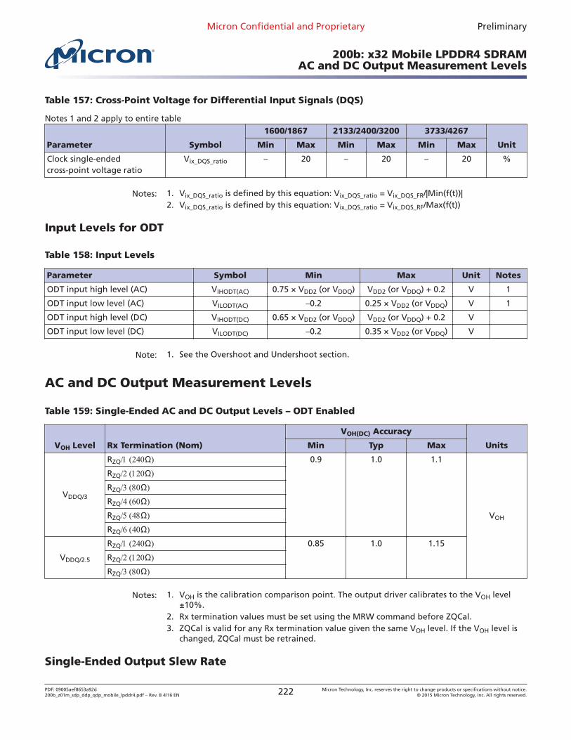
Table 157: Cross-Point Voltage for Differential Input Signals (DQS)
Notes 1 and 2 apply to entire table
Parameter Symbol
1600/1867 2133/2400/3200 3733/4267
UnitMin Max Min Max Min Max
Clock single-endedcross-point voltage ratio
Vix_DQS_ratio – 20 – 20 – 20 %
Notes: 1. Vix_DQS_ratio is defined by this equation: Vix_DQS_ratio = Vix_DQS_FR/|Min(f(t))|2. Vix_DQS_ratio is defined by this equation: Vix_DQS_ratio = Vix_DQS_RF/Max(f(t))
Input Levels for ODT
Table 158: Input Levels
Parameter Symbol Min Max Unit Notes
ODT input high level (AC) VIHODT(AC) 0.75 × VDD2 (or VDDQ) VDD2 (or VDDQ) + 0.2 V 1
ODT input low level (AC) VILODT(AC) –0.2 0.25 × VDD2 (or VDDQ) V 1
ODT input high level (DC) VIHODT(DC) 0.65 × VDD2 (or VDDQ) VDD2 (or VDDQ) + 0.2 V
ODT input low level (DC) VILODT(DC) –0.2 0.35 × VDD2 (or VDDQ) V
Note: 1. See the Overshoot and Undershoot section.
AC and DC Output Measurement Levels
Table 159: Single-Ended AC and DC Output Levels – ODT Enabled
VOH Level Rx Termination (Nom)
VOH(DC) Accuracy
UnitsMin Typ Max
VDDQ/3
RZQΩ 0.9 1.0 1.1
VOH
RZQΩ
RZQΩ
RZQΩ
RZQΩ
RZQΩ
VDDQ/2.5
RZQΩ 0.85 1.0 1.15
RZQΩ
RZQΩ
Notes: 1. VOH is the calibration comparison point. The output driver calibrates to the VOH level±10%.
2. Rx termination values must be set using the MRW command before ZQCal.3. ZQCal is valid for any Rx termination value given the same VOH level. If the VOH level is
changed, ZQCal must be retrained.
Single-Ended Output Slew Rate
Micron Confidential and Proprietary Preliminary
200b: x32 Mobile LPDDR4 SDRAMAC and DC Output Measurement Levels
PDF: 09005aef8653a92d200b_z01m_sdp_ddp_qdp_mobile_lpddr4.pdf – Rev. B 4/16 EN 222 Micron Technology, Inc. reserves the right to change products or specifications without notice.
© 2015 Micron Technology, Inc. All rights reserved.
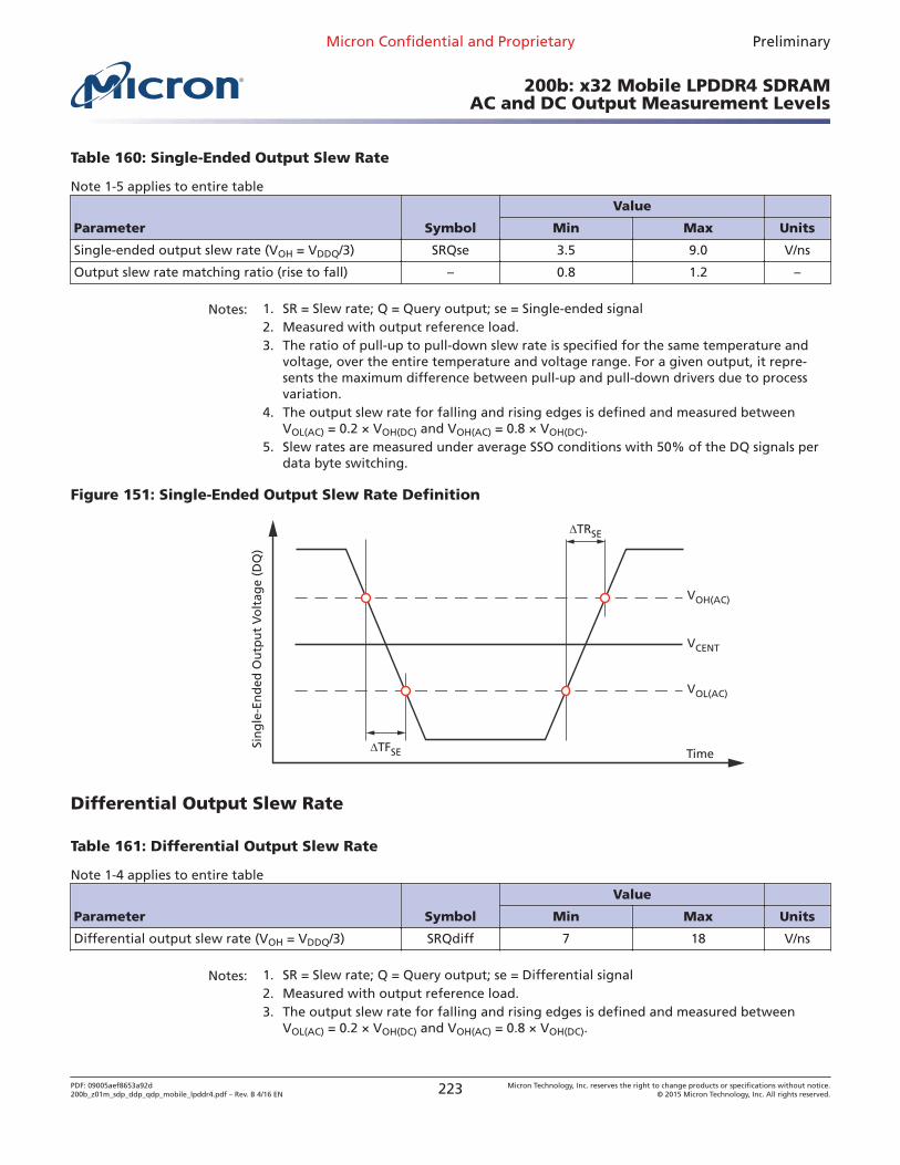
Table 160: Single-Ended Output Slew Rate
Note 1-5 applies to entire table
Parameter Symbol
Value
Min Max Units
Single-ended output slew rate (VOH = VDDQ/3) SRQse 3.5 9.0 V/ns
Output slew rate matching ratio (rise to fall) – 0.8 1.2 –
Notes: 1. SR = Slew rate; Q = Query output; se = Single-ended signal2. Measured with output reference load.3. The ratio of pull-up to pull-down slew rate is specified for the same temperature and
voltage, over the entire temperature and voltage range. For a given output, it repre-sents the maximum difference between pull-up and pull-down drivers due to processvariation.
4. The output slew rate for falling and rising edges is defined and measured betweenVOL(AC) = 0.2 × VOH(DC) and VOH(AC) = 0.8 × VOH(DC).
5. Slew rates are measured under average SSO conditions with 50% of the DQ signals perdata byte switching.
Figure 151: Single-Ended Output Slew Rate Definition
VOH(AC)
VCENT
VOL(AC)
Time
Sin
gle
-En
ded
Ou
tpu
t V
olt
age
(DQ
)
TFSE
TRSE
Differential Output Slew Rate
Table 161: Differential Output Slew Rate
Note 1-4 applies to entire table
Parameter Symbol
Value
Min Max Units
Differential output slew rate (VOH = VDDQ/3) SRQdiff 7 18 V/ns
Notes: 1. SR = Slew rate; Q = Query output; se = Differential signal2. Measured with output reference load.3. The output slew rate for falling and rising edges is defined and measured between
VOL(AC) = 0.2 × VOH(DC) and VOH(AC) = 0.8 × VOH(DC).
Micron Confidential and Proprietary Preliminary
200b: x32 Mobile LPDDR4 SDRAMAC and DC Output Measurement Levels
PDF: 09005aef8653a92d200b_z01m_sdp_ddp_qdp_mobile_lpddr4.pdf – Rev. B 4/16 EN 223 Micron Technology, Inc. reserves the right to change products or specifications without notice.
© 2015 Micron Technology, Inc. All rights reserved.
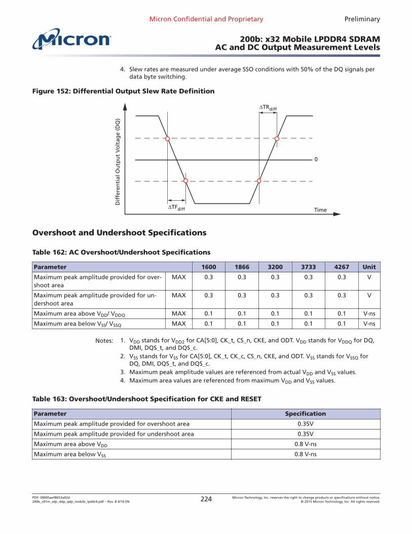
4. Slew rates are measured under average SSO conditions with 50% of the DQ signals perdata byte switching.
Figure 152: Differential Output Slew Rate Definition
0
Time
Dif
fere
nti
al O
utp
ut
Vo
ltag
e (D
Q)
TFdiff
TRdiff
Overshoot and Undershoot Specifications
Table 162: AC Overshoot/Undershoot Specifications
Parameter 1600 1866 3200 3733 4267 Unit
Maximum peak amplitude provided for over-shoot area
MAX 0.3 0.3 0.3 0.3 0.3 V
Maximum peak amplitude provided for un-dershoot area
MAX 0.3 0.3 0.3 0.3 0.3 V
Maximum area above VDD/ VDDQ MAX 0.1 0.1 0.1 0.1 0.1 V-ns
Maximum area below VSS/ VSSQ MAX 0.1 0.1 0.1 0.1 0.1 V-ns
Notes: 1. VDD stands for VDD2 for CA[5:0], CK_t, CS_n, CKE, and ODT. VDD stands for VDDQ for DQ,DMI, DQS_t, and DQS_c.
2. VSS stands for VSS for CA[5:0], CK_t, CK_c, CS_n, CKE, and ODT. VSS stands for VSSQ forDQ, DMI, DQS_t, and DQS_c.
3. Maximum peak amplitude values are referenced from actual VDD and VSS values.4. Maximum area values are referenced from maximum VDD and VSS values.
Table 163: Overshoot/Undershoot Specification for CKE and RESET
Parameter Specification
Maximum peak amplitude provided for overshoot area 0.35V
Maximum peak amplitude provided for undershoot area 0.35V
Maximum area above VDD 0.8 V-ns
Maximum area below VSS 0.8 V-ns
Micron Confidential and Proprietary Preliminary
200b: x32 Mobile LPDDR4 SDRAMAC and DC Output Measurement Levels
PDF: 09005aef8653a92d200b_z01m_sdp_ddp_qdp_mobile_lpddr4.pdf – Rev. B 4/16 EN 224 Micron Technology, Inc. reserves the right to change products or specifications without notice.
© 2015 Micron Technology, Inc. All rights reserved.
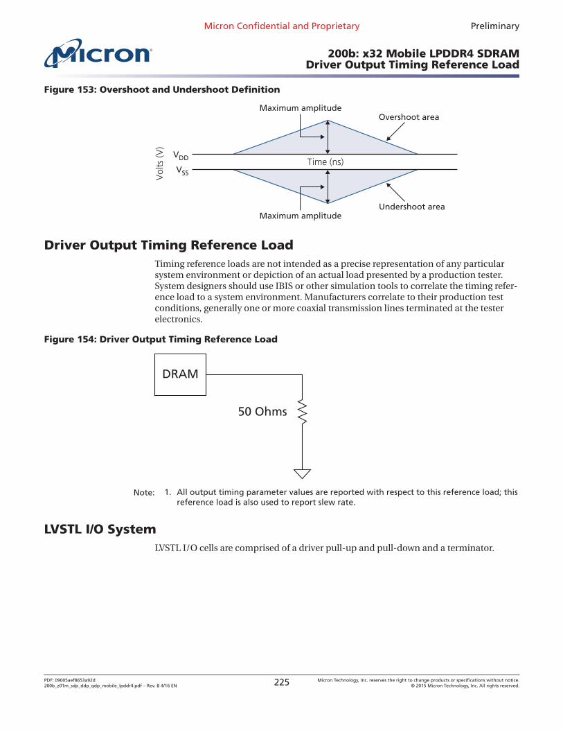
Figure 153: Overshoot and Undershoot Definition
Overshoot area
VDD
VSSVol
ts (V
)
Undershoot area
Maximum amplitude
Maximum amplitude
Time (ns)
Driver Output Timing Reference LoadTiming reference loads are not intended as a precise representation of any particularsystem environment or depiction of an actual load presented by a production tester.System designers should use IBIS or other simulation tools to correlate the timing refer-ence load to a system environment. Manufacturers correlate to their production testconditions, generally one or more coaxial transmission lines terminated at the testerelectronics.
Figure 154: Driver Output Timing Reference Load
50 Ohms
DRAM
Note: 1. All output timing parameter values are reported with respect to this reference load; thisreference load is also used to report slew rate.
LVSTL I/O SystemLVSTL I/O cells are comprised of a driver pull-up and pull-down and a terminator.
Micron Confidential and Proprietary Preliminary
200b: x32 Mobile LPDDR4 SDRAMDriver Output Timing Reference Load
PDF: 09005aef8653a92d200b_z01m_sdp_ddp_qdp_mobile_lpddr4.pdf – Rev. B 4/16 EN 225 Micron Technology, Inc. reserves the right to change products or specifications without notice.
© 2015 Micron Technology, Inc. All rights reserved.
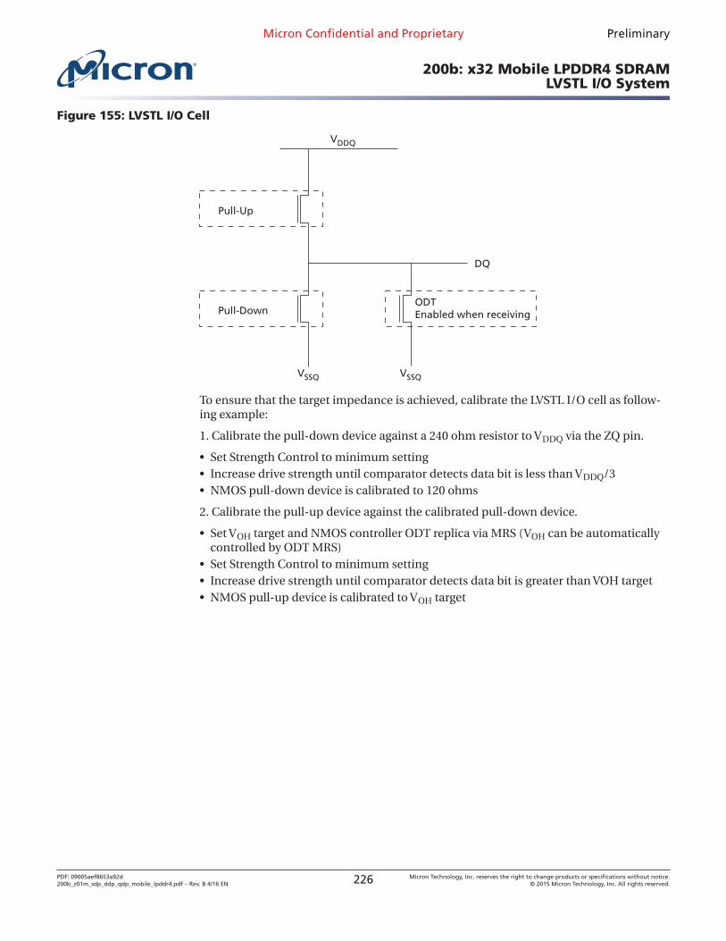
Figure 155: LVSTL I/O Cell
DQ
VSSQ
VDDQ
ODTEnabled when receiving
Pull-Up
Pull-Down
VSSQ
To ensure that the target impedance is achieved, calibrate the LVSTL I/O cell as follow-ing example:
1. Calibrate the pull-down device against a 240 ohm resistor to VDDQ via the ZQ pin.
• Set Strength Control to minimum setting• Increase drive strength until comparator detects data bit is less than VDDQ/3• NMOS pull-down device is calibrated to 120 ohms
2. Calibrate the pull-up device against the calibrated pull-down device.
• Set VOH target and NMOS controller ODT replica via MRS (VOH can be automaticallycontrolled by ODT MRS)
• Set Strength Control to minimum setting• Increase drive strength until comparator detects data bit is greater than VOH target• NMOS pull-up device is calibrated to VOH target
Micron Confidential and Proprietary Preliminary
200b: x32 Mobile LPDDR4 SDRAMLVSTL I/O System
PDF: 09005aef8653a92d200b_z01m_sdp_ddp_qdp_mobile_lpddr4.pdf – Rev. B 4/16 EN 226 Micron Technology, Inc. reserves the right to change products or specifications without notice.
© 2015 Micron Technology, Inc. All rights reserved.
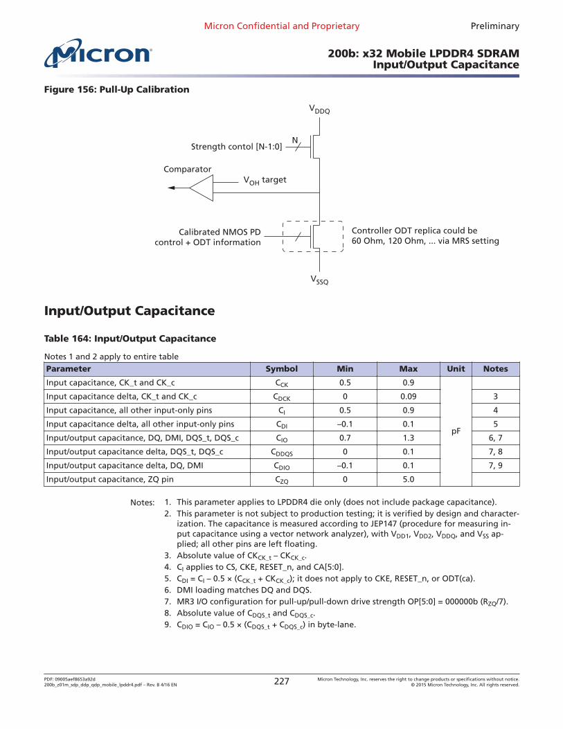
Figure 156: Pull-Up Calibration
VOH target
Calibrated NMOS PDcontrol + ODT information
Controller ODT replica could be 60 Ohm, 120 Ohm, ... via MRS setting
Strength contol [N-1:0]N
VSSQ
VDDQ
Comparator
Input/Output Capacitance
Table 164: Input/Output Capacitance
Notes 1 and 2 apply to entire tableParameter Symbol Min Max Unit Notes
Input capacitance, CK_t and CK_c CCK 0.5 0.9
pF
Input capacitance delta, CK_t and CK_c CDCK 0 0.09 3
Input capacitance, all other input-only pins CI 0.5 0.9 4
Input capacitance delta, all other input-only pins CDI –0.1 0.1 5
Input/output capacitance, DQ, DMI, DQS_t, DQS_c CIO 0.7 1.3 6, 7
Input/output capacitance delta, DQS_t, DQS_c CDDQS 0 0.1 7, 8
Input/output capacitance delta, DQ, DMI CDIO –0.1 0.1 7, 9
Input/output capacitance, ZQ pin CZQ 0 5.0
Notes: 1. This parameter applies to LPDDR4 die only (does not include package capacitance).2. This parameter is not subject to production testing; it is verified by design and character-
ization. The capacitance is measured according to JEP147 (procedure for measuring in-put capacitance using a vector network analyzer), with VDD1, VDD2, VDDQ, and VSS ap-plied; all other pins are left floating.
3. Absolute value of CKCK_t – CKCK_c.4. CI applies to CS, CKE, RESET_n, and CA[5:0].5. CDI = CI – 0.5 × (CCK_t + CKCK_c); it does not apply to CKE, RESET_n, or ODT(ca).6. DMI loading matches DQ and DQS.7. MR3 I/O configuration for pull-up/pull-down drive strength OP[5:0] = 000000b (RZQ/7).8. Absolute value of CDQS_t and CDQS_c.9. CDIO = CIO – 0.5 × (CDQS_t + CDQS_c) in byte-lane.
Micron Confidential and Proprietary Preliminary
200b: x32 Mobile LPDDR4 SDRAMInput/Output Capacitance
PDF: 09005aef8653a92d200b_z01m_sdp_ddp_qdp_mobile_lpddr4.pdf – Rev. B 4/16 EN 227 Micron Technology, Inc. reserves the right to change products or specifications without notice.
© 2015 Micron Technology, Inc. All rights reserved.
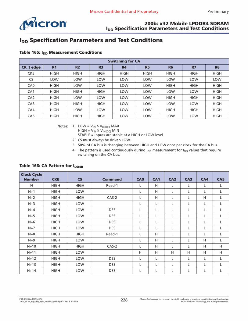
IDD Specification Parameters and Test Conditions
Table 165: IDD Measurement Conditions
Switching for CA
CK_t edge R1 R2 R3 R4 R5 R6 R7 R8
CKE HIGH HIGH HIGH HIGH HIGH HIGH HIGH HIGH
CS LOW LOW LOW LOW LOW LOW LOW LOW
CA0 HIGH LOW LOW LOW LOW HIGH HIGH HIGH
CA1 HIGH HIGH HIGH LOW LOW LOW LOW HIGH
CA2 HIGH LOW LOW LOW LOW HIGH HIGH HIGH
CA3 HIGH HIGH HIGH LOW LOW LOW LOW HIGH
CA4 HIGH LOW LOW LOW LOW HIGH HIGH HIGH
CA5 HIGH HIGH HIGH LOW LOW LOW LOW HIGH
Notes: 1. LOW = VIN ≤ VIL(DC) MAXHIGH = VIN ≥ VIH(DC) MINSTABLE = Inputs are stable at a HIGH or LOW level
2. CS must always be driven LOW.3. 50% of CA bus is changing between HIGH and LOW once per clock for the CA bus.4. The pattern is used continuously during IDD measurement for IDD values that require
switching on the CA bus.
Table 166: CA Pattern for IDD4R
Clock CycleNumber CKE CS Command CA0 CA1 CA2 CA3 CA4 CA5
N HIGH HIGH Read-1 L H L L L L
N+1 HIGH LOW L H L L L L
N+2 HIGH HIGH CAS-2 L H L L H L
N+3 HIGH LOW L L L L L L
N+4 HIGH LOW DES L L L L L L
N+5 HIGH LOW DES L L L L L L
N+6 HIGH LOW DES L L L L L L
N+7 HIGH LOW DES L L L L L L
N+8 HIGH HIGH Read-1 L H L L L L
N+9 HIGH LOW L H L L H L
N+10 HIGH HIGH CAS-2 L H L L H H
N+11 HIGH LOW H H H H H H
N+12 HIGH LOW DES L L L L L L
N+13 HIGH LOW DES L L L L L L
N+14 HIGH LOW DES L L L L L L
Micron Confidential and Proprietary Preliminary
200b: x32 Mobile LPDDR4 SDRAMIDD Specification Parameters and Test Conditions
PDF: 09005aef8653a92d200b_z01m_sdp_ddp_qdp_mobile_lpddr4.pdf – Rev. B 4/16 EN 228 Micron Technology, Inc. reserves the right to change products or specifications without notice.
© 2015 Micron Technology, Inc. All rights reserved.
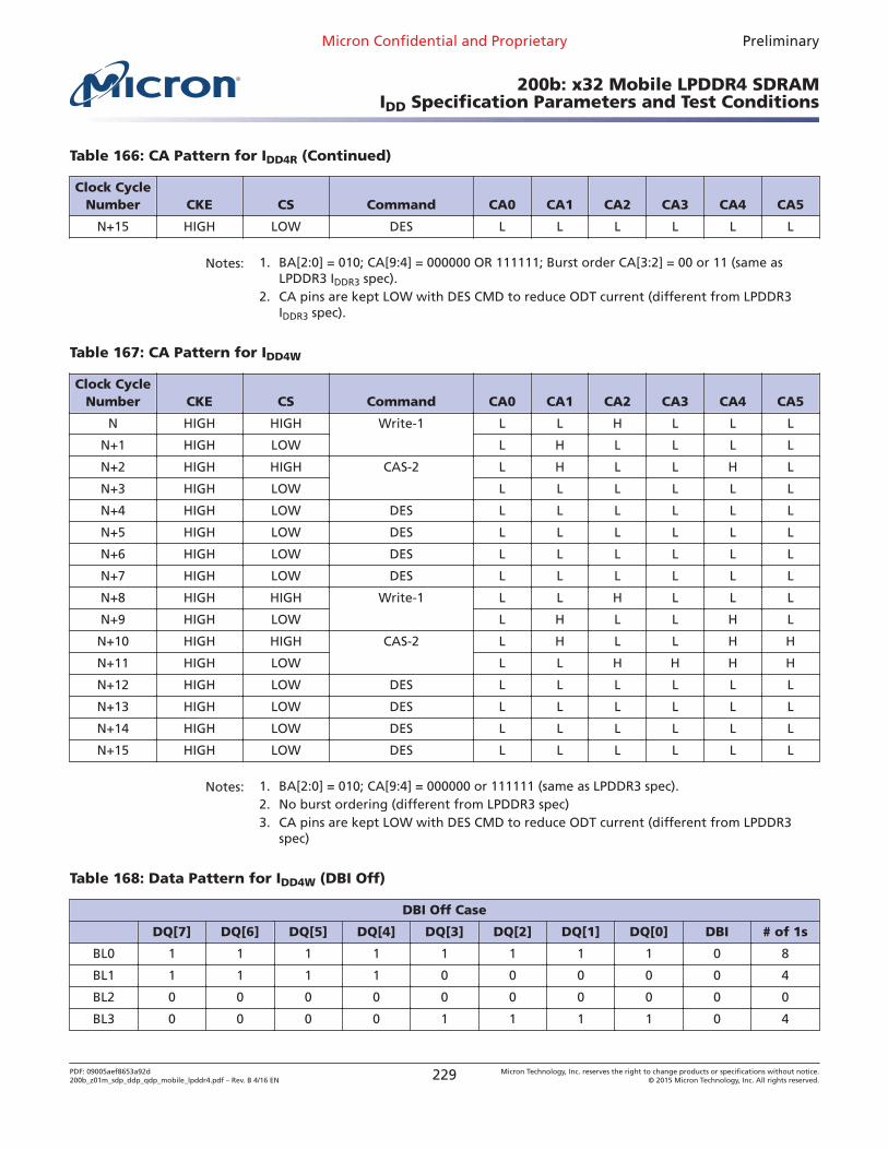
Table 166: CA Pattern for IDD4R (Continued)
Clock CycleNumber CKE CS Command CA0 CA1 CA2 CA3 CA4 CA5
N+15 HIGH LOW DES L L L L L L
Notes: 1. BA[2:0] = 010; CA[9:4] = 000000 OR 111111; Burst order CA[3:2] = 00 or 11 (same asLPDDR3 IDDR3 spec).
2. CA pins are kept LOW with DES CMD to reduce ODT current (different from LPDDR3IDDR3 spec).
Table 167: CA Pattern for IDD4W
Clock CycleNumber CKE CS Command CA0 CA1 CA2 CA3 CA4 CA5
N HIGH HIGH Write-1 L L H L L L
N+1 HIGH LOW L H L L L L
N+2 HIGH HIGH CAS-2 L H L L H L
N+3 HIGH LOW L L L L L L
N+4 HIGH LOW DES L L L L L L
N+5 HIGH LOW DES L L L L L L
N+6 HIGH LOW DES L L L L L L
N+7 HIGH LOW DES L L L L L L
N+8 HIGH HIGH Write-1 L L H L L L
N+9 HIGH LOW L H L L H L
N+10 HIGH HIGH CAS-2 L H L L H H
N+11 HIGH LOW L L H H H H
N+12 HIGH LOW DES L L L L L L
N+13 HIGH LOW DES L L L L L L
N+14 HIGH LOW DES L L L L L L
N+15 HIGH LOW DES L L L L L L
Notes: 1. BA[2:0] = 010; CA[9:4] = 000000 or 111111 (same as LPDDR3 spec).2. No burst ordering (different from LPDDR3 spec)3. CA pins are kept LOW with DES CMD to reduce ODT current (different from LPDDR3
spec)
Table 168: Data Pattern for IDD4W (DBI Off)
DBI Off Case
DQ[7] DQ[6] DQ[5] DQ[4] DQ[3] DQ[2] DQ[1] DQ[0] DBI # of 1s
BL0 1 1 1 1 1 1 1 1 0 8
BL1 1 1 1 1 0 0 0 0 0 4
BL2 0 0 0 0 0 0 0 0 0 0
BL3 0 0 0 0 1 1 1 1 0 4
Micron Confidential and Proprietary Preliminary
200b: x32 Mobile LPDDR4 SDRAMIDD Specification Parameters and Test Conditions
PDF: 09005aef8653a92d200b_z01m_sdp_ddp_qdp_mobile_lpddr4.pdf – Rev. B 4/16 EN 229 Micron Technology, Inc. reserves the right to change products or specifications without notice.
© 2015 Micron Technology, Inc. All rights reserved.
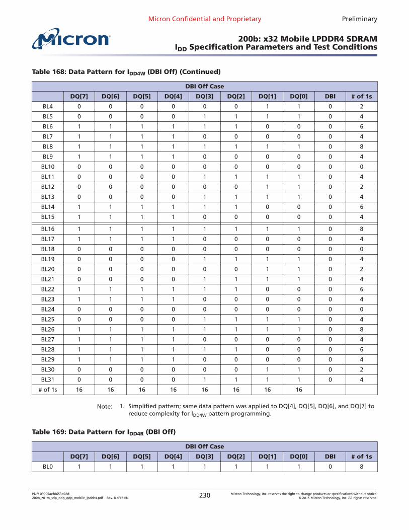
Table 168: Data Pattern for IDD4W (DBI Off) (Continued)
DBI Off Case
DQ[7] DQ[6] DQ[5] DQ[4] DQ[3] DQ[2] DQ[1] DQ[0] DBI # of 1s
BL4 0 0 0 0 0 0 1 1 0 2
BL5 0 0 0 0 1 1 1 1 0 4
BL6 1 1 1 1 1 1 0 0 0 6
BL7 1 1 1 1 0 0 0 0 0 4
BL8 1 1 1 1 1 1 1 1 0 8
BL9 1 1 1 1 0 0 0 0 0 4
BL10 0 0 0 0 0 0 0 0 0 0
BL11 0 0 0 0 1 1 1 1 0 4
BL12 0 0 0 0 0 0 1 1 0 2
BL13 0 0 0 0 1 1 1 1 0 4
BL14 1 1 1 1 1 1 0 0 0 6
BL15 1 1 1 1 0 0 0 0 0 4
BL16 1 1 1 1 1 1 1 1 0 8
BL17 1 1 1 1 0 0 0 0 0 4
BL18 0 0 0 0 0 0 0 0 0 0
BL19 0 0 0 0 1 1 1 1 0 4
BL20 0 0 0 0 0 0 1 1 0 2
BL21 0 0 0 0 1 1 1 1 0 4
BL22 1 1 1 1 1 1 0 0 0 6
BL23 1 1 1 1 0 0 0 0 0 4
BL24 0 0 0 0 0 0 0 0 0 0
BL25 0 0 0 0 1 1 1 1 0 4
BL26 1 1 1 1 1 1 1 1 0 8
BL27 1 1 1 1 0 0 0 0 0 4
BL28 1 1 1 1 1 1 0 0 0 6
BL29 1 1 1 1 0 0 0 0 0 4
BL30 0 0 0 0 0 0 1 1 0 2
BL31 0 0 0 0 1 1 1 1 0 4
# of 1s 16 16 16 16 16 16 16 16
Note: 1. Simplified pattern; same data pattern was applied to DQ[4], DQ[5], DQ[6], and DQ[7] toreduce complexity for IDD4W pattern programming.
Table 169: Data Pattern for IDD4R (DBI Off)
DBI Off Case
DQ[7] DQ[6] DQ[5] DQ[4] DQ[3] DQ[2] DQ[1] DQ[0] DBI # of 1s
BL0 1 1 1 1 1 1 1 1 0 8
Micron Confidential and Proprietary Preliminary
200b: x32 Mobile LPDDR4 SDRAMIDD Specification Parameters and Test Conditions
PDF: 09005aef8653a92d200b_z01m_sdp_ddp_qdp_mobile_lpddr4.pdf – Rev. B 4/16 EN 230 Micron Technology, Inc. reserves the right to change products or specifications without notice.
© 2015 Micron Technology, Inc. All rights reserved.
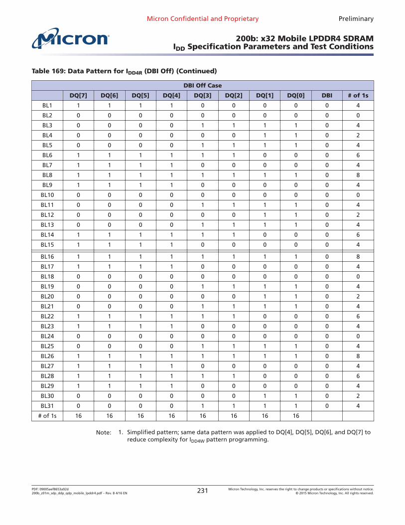
Table 169: Data Pattern for IDD4R (DBI Off) (Continued)
DBI Off Case
DQ[7] DQ[6] DQ[5] DQ[4] DQ[3] DQ[2] DQ[1] DQ[0] DBI # of 1s
BL1 1 1 1 1 0 0 0 0 0 4
BL2 0 0 0 0 0 0 0 0 0 0
BL3 0 0 0 0 1 1 1 1 0 4
BL4 0 0 0 0 0 0 1 1 0 2
BL5 0 0 0 0 1 1 1 1 0 4
BL6 1 1 1 1 1 1 0 0 0 6
BL7 1 1 1 1 0 0 0 0 0 4
BL8 1 1 1 1 1 1 1 1 0 8
BL9 1 1 1 1 0 0 0 0 0 4
BL10 0 0 0 0 0 0 0 0 0 0
BL11 0 0 0 0 1 1 1 1 0 4
BL12 0 0 0 0 0 0 1 1 0 2
BL13 0 0 0 0 1 1 1 1 0 4
BL14 1 1 1 1 1 1 0 0 0 6
BL15 1 1 1 1 0 0 0 0 0 4
BL16 1 1 1 1 1 1 1 1 0 8
BL17 1 1 1 1 0 0 0 0 0 4
BL18 0 0 0 0 0 0 0 0 0 0
BL19 0 0 0 0 1 1 1 1 0 4
BL20 0 0 0 0 0 0 1 1 0 2
BL21 0 0 0 0 1 1 1 1 0 4
BL22 1 1 1 1 1 1 0 0 0 6
BL23 1 1 1 1 0 0 0 0 0 4
BL24 0 0 0 0 0 0 0 0 0 0
BL25 0 0 0 0 1 1 1 1 0 4
BL26 1 1 1 1 1 1 1 1 0 8
BL27 1 1 1 1 0 0 0 0 0 4
BL28 1 1 1 1 1 1 0 0 0 6
BL29 1 1 1 1 0 0 0 0 0 4
BL30 0 0 0 0 0 0 1 1 0 2
BL31 0 0 0 0 1 1 1 1 0 4
# of 1s 16 16 16 16 16 16 16 16
Note: 1. Simplified pattern; same data pattern was applied to DQ[4], DQ[5], DQ[6], and DQ[7] toreduce complexity for IDD4W pattern programming.
Micron Confidential and Proprietary Preliminary
200b: x32 Mobile LPDDR4 SDRAMIDD Specification Parameters and Test Conditions
PDF: 09005aef8653a92d200b_z01m_sdp_ddp_qdp_mobile_lpddr4.pdf – Rev. B 4/16 EN 231 Micron Technology, Inc. reserves the right to change products or specifications without notice.
© 2015 Micron Technology, Inc. All rights reserved.
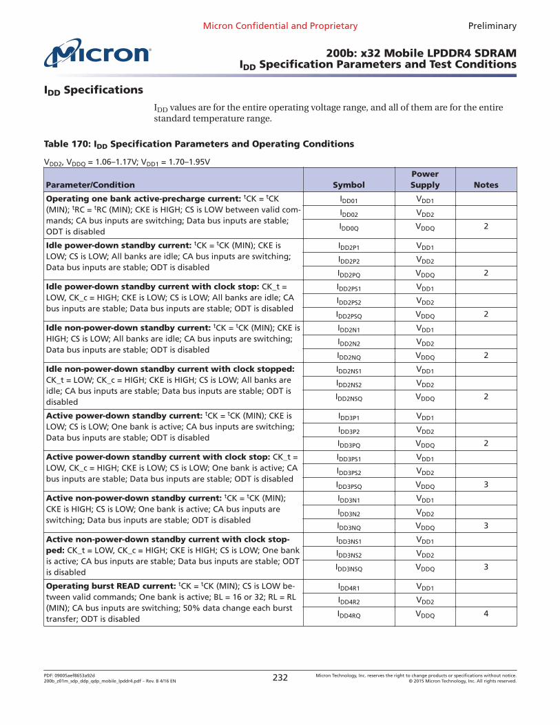
IDD Specifications
IDD values are for the entire operating voltage range, and all of them are for the entirestandard temperature range.
Table 170: IDD Specification Parameters and Operating Conditions
VDD2, VDDQ = 1.06–1.17V; VDD1 = 1.70–1.95V
Parameter/Condition SymbolPowerSupply Notes
Operating one bank active-precharge current: tCK = tCK(MIN); tRC = tRC (MIN); CKE is HIGH; CS is LOW between valid com-mands; CA bus inputs are switching; Data bus inputs are stable;ODT is disabled
IDD01 VDD1
IDD02 VDD2
IDD0Q VDDQ 2
Idle power-down standby current: tCK = tCK (MIN); CKE isLOW; CS is LOW; All banks are idle; CA bus inputs are switching;Data bus inputs are stable; ODT is disabled
IDD2P1 VDD1
IDD2P2 VDD2
IDD2PQ VDDQ 2
Idle power-down standby current with clock stop: CK_t =LOW, CK_c = HIGH; CKE is LOW; CS is LOW; All banks are idle; CAbus inputs are stable; Data bus inputs are stable; ODT is disabled
IDD2PS1 VDD1
IDD2PS2 VDD2
IDD2PSQ VDDQ 2
Idle non-power-down standby current: tCK = tCK (MIN); CKE isHIGH; CS is LOW; All banks are idle; CA bus inputs are switching;Data bus inputs are stable; ODT is disabled
IDD2N1 VDD1
IDD2N2 VDD2
IDD2NQ VDDQ 2
Idle non-power-down standby current with clock stopped:CK_t = LOW; CK_c = HIGH; CKE is HIGH; CS is LOW; All banks areidle; CA bus inputs are stable; Data bus inputs are stable; ODT isdisabled
IDD2NS1 VDD1
IDD2NS2 VDD2
IDD2NSQ VDDQ 2
Active power-down standby current: tCK = tCK (MIN); CKE isLOW; CS is LOW; One bank is active; CA bus inputs are switching;Data bus inputs are stable; ODT is disabled
IDD3P1 VDD1
IDD3P2 VDD2
IDD3PQ VDDQ 2
Active power-down standby current with clock stop: CK_t =LOW, CK_c = HIGH; CKE is LOW; CS is LOW; One bank is active; CAbus inputs are stable; Data bus inputs are stable; ODT is disabled
IDD3PS1 VDD1
IDD3PS2 VDD2
IDD3PSQ VDDQ 3
Active non-power-down standby current: tCK = tCK (MIN);CKE is HIGH; CS is LOW; One bank is active; CA bus inputs areswitching; Data bus inputs are stable; ODT is disabled
IDD3N1 VDD1
IDD3N2 VDD2
IDD3NQ VDDQ 3
Active non-power-down standby current with clock stop-ped: CK_t = LOW, CK_c = HIGH; CKE is HIGH; CS is LOW; One bankis active; CA bus inputs are stable; Data bus inputs are stable; ODTis disabled
IDD3NS1 VDD1
IDD3NS2 VDD2
IDD3NSQ VDDQ 3
Operating burst READ current: tCK = tCK (MIN); CS is LOW be-tween valid commands; One bank is active; BL = 16 or 32; RL = RL(MIN); CA bus inputs are switching; 50% data change each bursttransfer; ODT is disabled
IDD4R1 VDD1
IDD4R2 VDD2
IDD4RQ VDDQ 4
Micron Confidential and Proprietary Preliminary
200b: x32 Mobile LPDDR4 SDRAMIDD Specification Parameters and Test Conditions
PDF: 09005aef8653a92d200b_z01m_sdp_ddp_qdp_mobile_lpddr4.pdf – Rev. B 4/16 EN 232 Micron Technology, Inc. reserves the right to change products or specifications without notice.
© 2015 Micron Technology, Inc. All rights reserved.
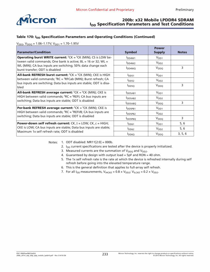
Table 170: IDD Specification Parameters and Operating Conditions (Continued)
VDD2, VDDQ = 1.06–1.17V; VDD1 = 1.70–1.95V
Parameter/Condition SymbolPowerSupply Notes
Operating burst WRITE current: tCK = tCK (MIN); CS is LOW be-tween valid commands; One bank is active; BL = 16 or 32; WL =WL (MIN); CA bus inputs are switching; 50% data change eachburst transfer; ODT is disabled
IDD4W1 VDD1
IDD4W2 VDD2
IDD4WQ VDDQ 3
All-bank REFRESH burst current: tCK = tCK (MIN); CKE is HIGHbetween valid commands; tRC = tRFCab (MIN); Burst refresh; CAbus inputs are switching; Data bus inputs are stable; ODT is disa-bled
IDD51 VDD1
IDD52 VDD2
IDD5Q VDDQ 3
All-bank REFRESH average current: tCK = tCK (MIN); CKE isHIGH between valid commands; tRC = tREFI; CA bus inputs areswitching; Data bus inputs are stable; ODT is disabled
IDD5AB1 VDD1
IDD5AB2 VDD2
IDD5ABQ VDDQ 3
Per-bank REFRESH average current: tCK = tCK (MIN); CKE isHIGH between valid commands; tRC = tREFI/8; CA bus inputs areswitching; Data bus inputs are stable; ODT is disabled
IDD5PB1 VDD1
IDD5PB2 VDD2
IDD5PBQ VDDQ 3
Power-down self refresh current: CK_t = LOW, CK_c = HIGH;CKE is LOW; CA bus inputs are stable; Data bus inputs are stable;Maximum 1x self refresh rate; ODT is disabled
IDD61 VDD1 5, 6
IDD62 VDD2 5, 6
IDD6Q VDDQ 3, 5, 6
Notes: 1. ODT disabled: MR11[2:0] = 000b.2. IDD current specifications are tested after the device is properly initialized.3. Measured currents are the summation of VDDQ and VDD2.4. Guaranteed by design with output load = 5pF and RON = 40 ohm.5. The 1x self refresh rate is the rate at which the device is refreshed internally during self
refresh before going into the elevated temperature range.6. This is the general definition that applies to full-array self refresh.7. For all IDD measurements, VIHCKE = 0.8 × VDD2; VILCKE = 0.2 × VDD2.
Micron Confidential and Proprietary Preliminary
200b: x32 Mobile LPDDR4 SDRAMIDD Specification Parameters and Test Conditions
PDF: 09005aef8653a92d200b_z01m_sdp_ddp_qdp_mobile_lpddr4.pdf – Rev. B 4/16 EN 233 Micron Technology, Inc. reserves the right to change products or specifications without notice.
© 2015 Micron Technology, Inc. All rights reserved.
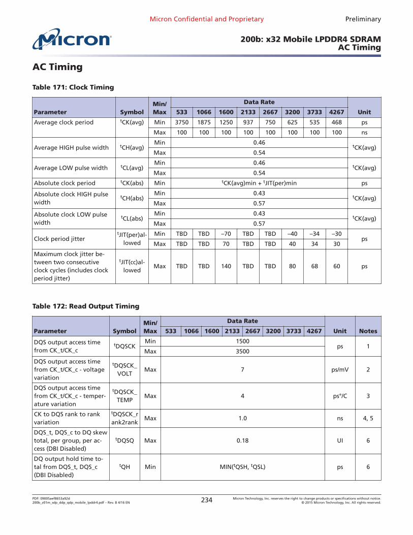
AC Timing
Table 171: Clock Timing
Parameter SymbolMin/Max
Data Rate
Unit533 1066 1600 2133 2667 3200 3733 4267
Average clock period tCK(avg) Min 3750 1875 1250 937 750 625 535 468 ps
Max 100 100 100 100 100 100 100 100 ns
Average HIGH pulse width tCH(avg)Min 0.46
tCK(avg)Max 0.54
Average LOW pulse width tCL(avg)Min 0.46
tCK(avg)Max 0.54
Absolute clock period tCK(abs) Min tCK(avg)min + tJIT(per)min ps
Absolute clock HIGH pulsewidth
tCH(abs)Min 0.43
tCK(avg)Max 0.57
Absolute clock LOW pulsewidth
tCL(abs)Min 0.43
tCK(avg)Max 0.57
Clock period jittertJIT(per)al-
lowed
Min TBD TBD –70 TBD TBD –40 –34 –30ps
Max TBD TBD 70 TBD TBD 40 34 30
Maximum clock jitter be-tween two consecutiveclock cycles (includes clockperiod jitter)
tJIT(cc)al-lowed
Max TBD TBD 140 TBD TBD 80 68 60 ps
Table 172: Read Output Timing
Parameter SymbolMin/Max
Data Rate
Unit Notes533 1066 1600 2133 2667 3200 3733 4267
DQS output access timefrom CK_t/CK_c
tDQSCKMin 1500
ps 1Max 3500
DQS output access timefrom CK_t/CK_c - voltagevariation
tDQSCK_VOLT
Max 7 ps/mV 2
DQS output access timefrom CK_t/CK_c - temper-ature variation
tDQSCK_TEMP
Max 4 ps°/C 3
CK to DQS rank to rankvariation
tDQSCK_rank2rank
Max 1.0 ns 4, 5
DQS_t, DQS_c to DQ skewtotal, per group, per ac-cess (DBI Disabled)
tDQSQ Max 0.18 UI 6
DQ output hold time to-tal from DQS_t, DQS_c(DBI Disabled)
tQH Min MIN(tQSH, tQSL) ps 6
Micron Confidential and Proprietary Preliminary
200b: x32 Mobile LPDDR4 SDRAMAC Timing
PDF: 09005aef8653a92d200b_z01m_sdp_ddp_qdp_mobile_lpddr4.pdf – Rev. B 4/16 EN 234 Micron Technology, Inc. reserves the right to change products or specifications without notice.
© 2015 Micron Technology, Inc. All rights reserved.
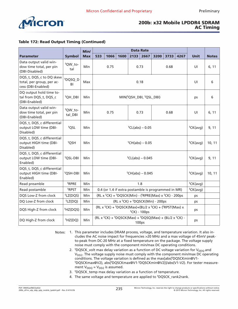
Table 172: Read Output Timing (Continued)
Parameter SymbolMin/Max
Data Rate
Unit Notes533 1066 1600 2133 2667 3200 3733 4267
Data output valid win-dow time total, per pin(DBI-Disabled)
tQW_to-tal
Min 0.75 0.73 0.68 UI 6, 11
DQS_t, DQS_c to DQ skewtotal, per group, per ac-cess (DBI-Enabled)
tDQSQ_DBI
Max 0.18 UI 6
DQ output hold time to-tal from DQS_t, DQS_c(DBI-Enabled)
tQH_DBI Min MIN(tQSH_DBI, tQSL_DBI) ps 6
Data output valid win-dow time total, per pin(DBI-Enabled)
tQW_to-tal_DBI
Min 0.75 0.73 0.68 UI 6, 11
DQS_t, DQS_c differentialoutput LOW time (DBI-Disabled)
tQSL Min tCL(abs) – 0.05 tCK(avg) 9, 11
DQS_t, DQS_c differentialoutput HIGH time (DBI-Disabled)
tQSH Min tCH(abs) – 0.05 tCK(avg) 10, 11
DQS_t, DQS_c differentialoutput LOW time (DBI-Enabled)
tQSL-DBI Min tCL(abs) – 0.045 tCK(avg) 9, 11
DQS_t, DQS_c differentialoutput HIGH time (DBI-Enabled)
tQSH-DBI Min tCH(abs) – 0.045 tCK(avg) 10, 11
Read preamble tRPRE Min 1.8 tCK(avg)
Read postamble tRPST Min 0.4 (or 1.4 if extra postamble is programmed in MR) tCK(avg)
DQS Low-Z from clock tLZ(DQS) Min (RL x tCK) + tDQSCK(Min) - (tRPRE(Max) x tCK) - 200ps ps
DQ Low-Z from clock tLZ(DQ) Min (RL x tCK) + tDQSCK(Min) - 200ps ps
DQS High-Z from clock tHZ(DQS) Min(RL x tCK) + tDQSCK(Max)+(BL/2 x tCK) + (tRPST(Max) x
tCK) - 100psps
DQ High-Z from clock tHZ(DQ) Min(RL x tCK) + tDQSCK(Max) + tDQSQ(Max) + (BL/2 x tCK) -
100psps
Notes: 1. This parameter includes DRAM process, voltage, and temperature variation. It also in-cludes the AC noise impact for frequencies >20 MHz and a max voltage of 45mV peak-to-peak from DC-20 MHz at a fixed temperature on the package. The voltage supplynoise must comply with the component min/max DC operating conditions.
2. tDQSCK_volt max delay variation as a function of DC voltage variation for VDDQ andVDD2. The voltage supply noise must comply with the component min/max DC operatingconditions. The voltage variation is defined as the max[abs(tDQSCKmin@V1-tDQSCKmax@V2), abs(tDQSCKmax@V1-tDQSCKmin@V2)]/abs(V1-V2). For tester measure-ment VDDQ = VDD2 is assumed.
3. tDQSCK_temp max delay variation as a function of temperature.4. The same voltage and temperature are applied to tDQSCK_rank2rank.
Micron Confidential and Proprietary Preliminary
200b: x32 Mobile LPDDR4 SDRAMAC Timing
PDF: 09005aef8653a92d200b_z01m_sdp_ddp_qdp_mobile_lpddr4.pdf – Rev. B 4/16 EN 235 Micron Technology, Inc. reserves the right to change products or specifications without notice.
© 2015 Micron Technology, Inc. All rights reserved.
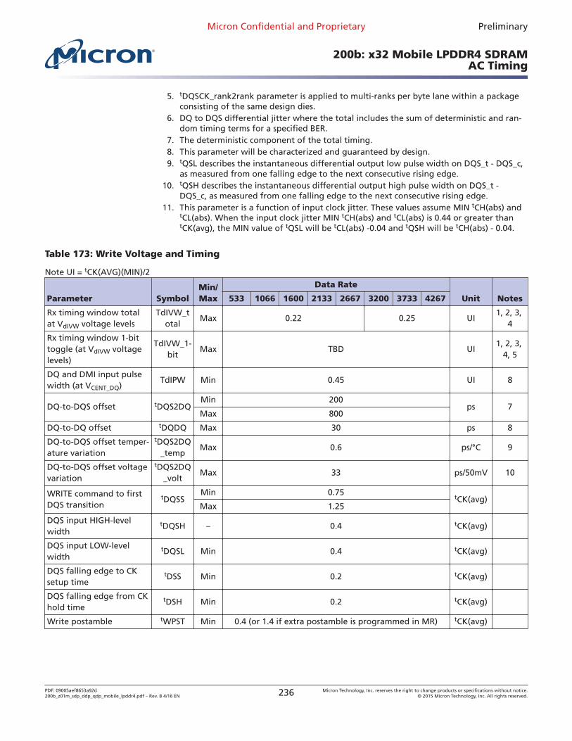
5. tDQSCK_rank2rank parameter is applied to multi-ranks per byte lane within a packageconsisting of the same design dies.
6. DQ to DQS differential jitter where the total includes the sum of deterministic and ran-dom timing terms for a specified BER.
7. The deterministic component of the total timing.8. This parameter will be characterized and guaranteed by design.9. tQSL describes the instantaneous differential output low pulse width on DQS_t - DQS_c,
as measured from one falling edge to the next consecutive rising edge.10. tQSH describes the instantaneous differential output high pulse width on DQS_t -
DQS_c, as measured from one falling edge to the next consecutive rising edge.11. This parameter is a function of input clock jitter. These values assume MIN tCH(abs) and
tCL(abs). When the input clock jitter MIN tCH(abs) and tCL(abs) is 0.44 or greater thantCK(avg), the MIN value of tQSL will be tCL(abs) -0.04 and tQSH will be tCH(abs) - 0.04.
Table 173: Write Voltage and Timing
Note UI = tCK(AVG)(MIN)/2
Parameter SymbolMin/Max
Data Rate
Unit Notes533 1066 1600 2133 2667 3200 3733 4267
Rx timing window totalat VdIVW voltage levels
TdIVW_total
Max 0.22 0.25 UI1, 2, 3,
4
Rx timing window 1-bittoggle (at VdIVW voltagelevels)
TdIVW_1-bit
Max TBD UI1, 2, 3,
4, 5
DQ and DMI input pulsewidth (at VCENT_DQ)
TdIPW Min 0.45 UI 8
DQ-to-DQS offset tDQS2DQMin 200
ps 7Max 800
DQ-to-DQ offset tDQDQ Max 30 ps 8
DQ-to-DQS offset temper-ature variation
tDQS2DQ_temp
Max 0.6 ps/°C 9
DQ-to-DQS offset voltagevariation
tDQS2DQ_volt
Max 33 ps/50mV 10
WRITE command to firstDQS transition
tDQSSMin 0.75
tCK(avg)Max 1.25
DQS input HIGH-levelwidth
tDQSH – 0.4 tCK(avg)
DQS input LOW-levelwidth
tDQSL Min 0.4 tCK(avg)
DQS falling edge to CKsetup time
tDSS Min 0.2 tCK(avg)
DQS falling edge from CKhold time
tDSH Min 0.2 tCK(avg)
Write postamble tWPST Min 0.4 (or 1.4 if extra postamble is programmed in MR) tCK(avg)
Micron Confidential and Proprietary Preliminary
200b: x32 Mobile LPDDR4 SDRAMAC Timing
PDF: 09005aef8653a92d200b_z01m_sdp_ddp_qdp_mobile_lpddr4.pdf – Rev. B 4/16 EN 236 Micron Technology, Inc. reserves the right to change products or specifications without notice.
© 2015 Micron Technology, Inc. All rights reserved.
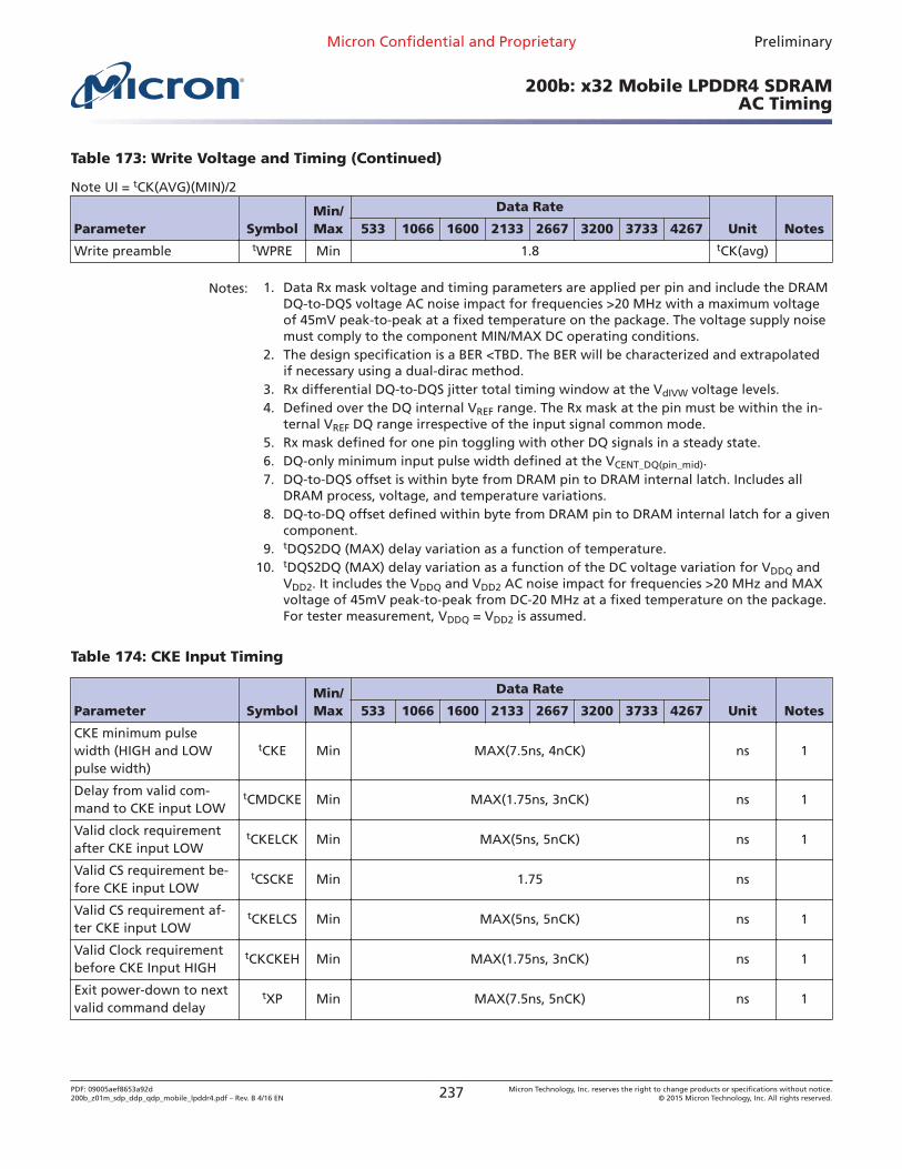
Table 173: Write Voltage and Timing (Continued)
Note UI = tCK(AVG)(MIN)/2
Parameter SymbolMin/Max
Data Rate
Unit Notes533 1066 1600 2133 2667 3200 3733 4267
Write preamble tWPRE Min 1.8 tCK(avg)
Notes: 1. Data Rx mask voltage and timing parameters are applied per pin and include the DRAMDQ-to-DQS voltage AC noise impact for frequencies >20 MHz with a maximum voltageof 45mV peak-to-peak at a fixed temperature on the package. The voltage supply noisemust comply to the component MIN/MAX DC operating conditions.
2. The design specification is a BER <TBD. The BER will be characterized and extrapolatedif necessary using a dual-dirac method.
3. Rx differential DQ-to-DQS jitter total timing window at the VdIVW voltage levels.4. Defined over the DQ internal VREF range. The Rx mask at the pin must be within the in-
ternal VREF DQ range irrespective of the input signal common mode.5. Rx mask defined for one pin toggling with other DQ signals in a steady state.6. DQ-only minimum input pulse width defined at the VCENT_DQ(pin_mid).7. DQ-to-DQS offset is within byte from DRAM pin to DRAM internal latch. Includes all
DRAM process, voltage, and temperature variations.8. DQ-to-DQ offset defined within byte from DRAM pin to DRAM internal latch for a given
component.9. tDQS2DQ (MAX) delay variation as a function of temperature.
10. tDQS2DQ (MAX) delay variation as a function of the DC voltage variation for VDDQ andVDD2. It includes the VDDQ and VDD2 AC noise impact for frequencies >20 MHz and MAXvoltage of 45mV peak-to-peak from DC-20 MHz at a fixed temperature on the package.For tester measurement, VDDQ = VDD2 is assumed.
Table 174: CKE Input Timing
Parameter SymbolMin/Max
Data Rate
Unit Notes533 1066 1600 2133 2667 3200 3733 4267
CKE minimum pulsewidth (HIGH and LOWpulse width)
tCKE Min MAX(7.5ns, 4nCK) ns 1
Delay from valid com-mand to CKE input LOW
tCMDCKE Min MAX(1.75ns, 3nCK) ns 1
Valid clock requirementafter CKE input LOW
tCKELCK Min MAX(5ns, 5nCK) ns 1
Valid CS requirement be-fore CKE input LOW
tCSCKE Min 1.75 ns
Valid CS requirement af-ter CKE input LOW
tCKELCS Min MAX(5ns, 5nCK) ns 1
Valid Clock requirementbefore CKE Input HIGH
tCKCKEH Min MAX(1.75ns, 3nCK) ns 1
Exit power-down to nextvalid command delay
tXP Min MAX(7.5ns, 5nCK) ns 1
Micron Confidential and Proprietary Preliminary
200b: x32 Mobile LPDDR4 SDRAMAC Timing
PDF: 09005aef8653a92d200b_z01m_sdp_ddp_qdp_mobile_lpddr4.pdf – Rev. B 4/16 EN 237 Micron Technology, Inc. reserves the right to change products or specifications without notice.
© 2015 Micron Technology, Inc. All rights reserved.
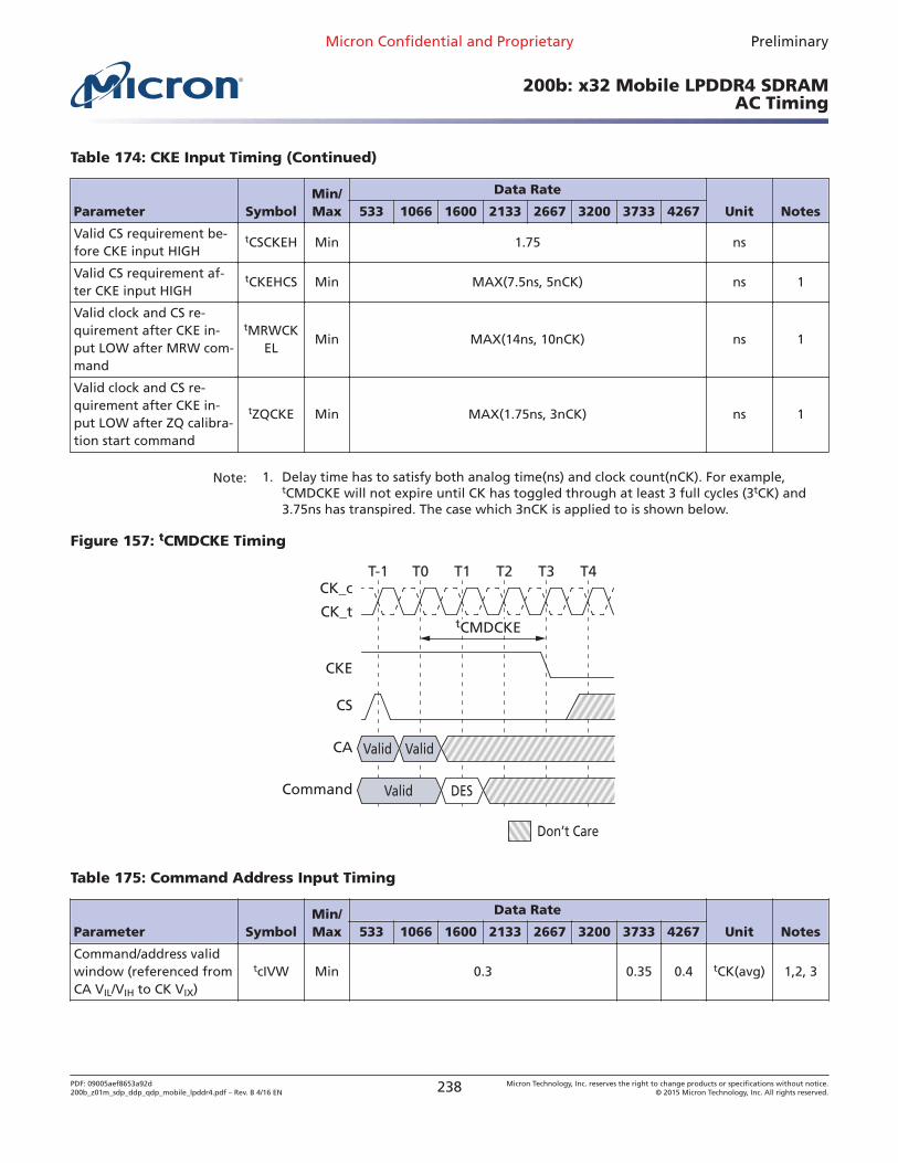
Table 174: CKE Input Timing (Continued)
Parameter SymbolMin/Max
Data Rate
Unit Notes533 1066 1600 2133 2667 3200 3733 4267
Valid CS requirement be-fore CKE input HIGH
tCSCKEH Min 1.75 ns
Valid CS requirement af-ter CKE input HIGH
tCKEHCS Min MAX(7.5ns, 5nCK) ns 1
Valid clock and CS re-quirement after CKE in-put LOW after MRW com-mand
tMRWCKEL
Min MAX(14ns, 10nCK) ns 1
Valid clock and CS re-quirement after CKE in-put LOW after ZQ calibra-tion start command
tZQCKE Min MAX(1.75ns, 3nCK) ns 1
Note: 1. Delay time has to satisfy both analog time(ns) and clock count(nCK). For example,tCMDCKE will not expire until CK has toggled through at least 3 full cycles (3tCK) and3.75ns has transpired. The case which 3nCK is applied to is shown below.
Figure 157: tCMDCKE Timing
T-1
CK_t
CK_cT0 T1 T2
CA Valid
T3 T4
Command DES
CS
CKE
Valid
Valid
tCMDCKE
Don’t Care
Table 175: Command Address Input Timing
Parameter SymbolMin/Max
Data Rate
Unit Notes533 1066 1600 2133 2667 3200 3733 4267
Command/address validwindow (referenced fromCA VIL/VIH to CK VIX)
tcIVW Min 0.3 0.35 0.4 tCK(avg) 1,2, 3
Micron Confidential and Proprietary Preliminary
200b: x32 Mobile LPDDR4 SDRAMAC Timing
PDF: 09005aef8653a92d200b_z01m_sdp_ddp_qdp_mobile_lpddr4.pdf – Rev. B 4/16 EN 238 Micron Technology, Inc. reserves the right to change products or specifications without notice.
© 2015 Micron Technology, Inc. All rights reserved.
Table 175: Command Address Input Timing (Continued)
Parameter SymbolMin/Max
Data Rate
Unit Notes533 1066 1600 2133 2667 3200 3733 4267
Address and control inputpulse width (referencedto VREF)
tcIPW Min 0.55 0.55 0.55 0.6 0.6 0.6 0.7 0.8 tCK(avg) 4
Notes: 1. CA Rx mask timing parameters at the pin including voltage and temperature drift.2. Rx differential CA to CK jitter total timing window at the VcIVW voltage levels.3. Defined over the CA internal VREF range. The Rx mask at the pin must be within the in-
ternal VREF(CA) range irrespective of the input signal common mode.4. CA only minimum input pulse width defined at the Vcent_CA(pin mid).
Table 176: Boot Timing Parameters (10–55 MHz)
Parameter SymbolMin/Max
Data Rate
Unit533 1066 1600 2133 2667 3200 3733 4267
Clock cycle time tCKbMin 18
nsMax 100
DQS output data acess timefrom CK
tDQSCKbMin 1.0
nsMax 10.0
DQS edge to output dataedge
tDQSQb Max 1.2 ns
Table 177: Mode Register Timing Parameters
Parameter SymbolMin/Max
Data Rate
Unit533 1066 1600 2133 2667 3200 3733 4267
MODE REGISTER WRITE(MRW) command period
tMRW Min MAX(10ns, 10nCK) ns
MODE REGISTER READ(MRR) command period
tMRR Min 8 tCK(avg)
Additional time after tXPhas expired until the MRRcommand may be issued
tMRRI Min tRCD(min) + 3nCK ns
Delay from MRW commandto DQS driven out
tSDO Max MAX(12nCK, 20ns) ns
Micron Confidential and Proprietary Preliminary
200b: x32 Mobile LPDDR4 SDRAMAC Timing
PDF: 09005aef8653a92d200b_z01m_sdp_ddp_qdp_mobile_lpddr4.pdf – Rev. B 4/16 EN 239 Micron Technology, Inc. reserves the right to change products or specifications without notice.
© 2015 Micron Technology, Inc. All rights reserved.
Table 178: Core Timing Parameters
Refresh rate is determined by the value in MR4 OP[2:0]
Parameter SymbolMin/Max
Data Rate
Unit Notes533 1066 1600 2133 2667 3200 3733 4267
READ latency (DBI disa-bled)
RL-A Min 6 10 14 20 24 28 32 36 tCK(avg)
READ latency (DBI ena-bled)
RL-B Min 6 12 16 22 28 32 36 40 tCK(avg)
WRITE latency (Set A) WL-A Min 4 6 8 10 12 14 16 18 tCK(avg)
WRITE latency (Set B) WL-B Min 4 8 12 18 22 26 30 34 tCK(avg)
ACTIVATE-to-ACTIVATEcommand period (samebank)
tRC Min
tRAS + tRPab(with all-bank precharge)
tRAS + tRPpb(with per-bank precharge)
ns
Minimum self refreshtime (entry to exit)
tSR Min MAX(15ns, 3nCK) ns
Self refresh exit to nextvalid command delay
tXSR Min MAX(tRFCab + 7.5ns, 2nCK) ns
CAS-to-CAS delay tCCD Min 8 tCK(avg)
CAS-to-CAS delay maskedwrite
tCCDMW MIN 32 tCK(avg)
Internal READ-to-PRE-CHARGE command delay
tRTP Min MAX(7.5ns, 8nCK) ns
RAS-to-CAS delay tRCD Min MAX(18ns, 4nCK) ns
Row precharge time (sin-gle bank)
tRPpb Min MAX(18ns, 3nCK) ns
Row precharge time (allbanks)
tRPab Min MAX(21ns, 3nCK) ns
Row active time tRASMin MAX(42ns, 3nCK) ns
Max MIN(9 × tREFI × Refresh Rate1, 70.2) μs
Write recovery time tWR Min MAX(18ns, 4nCK) ns
Write-to-read delay tWTR Min MAX(10ns, 8nCK) ns
Active bank A to activebank B
tRRD Min MAX(10ns, 4nCK) ns
Precharge-to-prechargedelay
tPPD Min 4 tCK(avg)
Four-bank activate win-dow
tFAW Min 40 ns
Delay from SRE commandto CKE input LOW
tESCKE Min MAX(1.75ns, 3nCK) – 1
Note: 1. Delay time has to satisfy both analog time(ns) and clock count (nCK). It means thattESCKE will not expire until CK has toggled through at least three full cycles (3 tCK) and1.75ns has transpired. The case which 3nCK is applied to is shown below.
Micron Confidential and Proprietary Preliminary
200b: x32 Mobile LPDDR4 SDRAMAC Timing
PDF: 09005aef8653a92d200b_z01m_sdp_ddp_qdp_mobile_lpddr4.pdf – Rev. B 4/16 EN 240 Micron Technology, Inc. reserves the right to change products or specifications without notice.
© 2015 Micron Technology, Inc. All rights reserved.
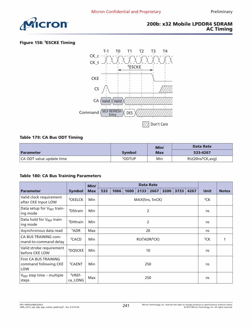
Figure 158: tESCKE Timing
T-1
CK_t
CK_cT0 T1 T2
CA Valid
T3 T4
Command DES
CS
CKE
Valid
Don’t Care
EntrySELF REFRESH
tESCKE
Table 179: CA Bus ODT Timing
Parameter SymbolMin/Max
Data Rate
533-4267
CA ODT value update time tODTUP Min RU(20ns/tCK,avg)
Table 180: CA Bus Training Parameters
Parameter SymbolMin/Max
Data Rate
Unit Notes533 1066 1600 2133 2667 3200 3733 4267
Valid clock requirementafter CKE Input LOW
tCKELCK Min MAX(5ns, 5nCK) tCK
Data setup for VREF train-ing mode
tDStrain Min 2 ns
Data hold for VREF train-ing mode
tDHtrain Min 2 ns
Asynchronous data read tADR Max 20 ns
CA BUS TRAINING com-mand-to-command delay
tCACD Min RU(tADR/tCK) tCK 1
Valid strobe requirementbefore CKE LOW
tDQSCKE Min 10 ns
First CA BUS TRAININGcommand following CKELOW
tCAENT Min 250 ns
VREF step time – multiplesteps
tVREF-ca_LONG
Max 250 ns
Micron Confidential and Proprietary Preliminary
200b: x32 Mobile LPDDR4 SDRAMAC Timing
PDF: 09005aef8653a92d200b_z01m_sdp_ddp_qdp_mobile_lpddr4.pdf – Rev. B 4/16 EN 241 Micron Technology, Inc. reserves the right to change products or specifications without notice.
© 2015 Micron Technology, Inc. All rights reserved.
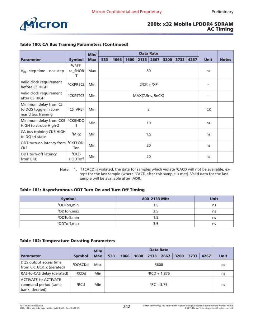
Table 180: CA Bus Training Parameters (Continued)
Parameter SymbolMin/Max
Data Rate
Unit Notes533 1066 1600 2133 2667 3200 3733 4267
VREF step time – one step
tVREF-ca_SHOR
TMax 80 ns
Valid clock requirementbefore CS HIGH
tCKPRECS Min 2tCK + tXP –
Valid clock requirementafter CS HIGH
tCKPSTCS Min MAX(7.5ns, 5nCK) –
Minimum delay from CSto DQS toggle in com-mand bus training
tCS_VREF Min 2 tCK
Minimum delay from CKEHIGH to strobe High-Z
tCKEHDQS
Min 10 ns
CA bus training CKE HIGHto DQ tri-state
tMRZ Min 1.5 ns
ODT turn-on latency fromCKE
tCKELOD-Ton
Min 20 ns
ODT turn-off latencyfrom CKE
tCKE-HODToff
Min 20 ns
Note: 1. If tCACD is violated, the data for samples which violate tCACD will not be available, ex-cept for the last sample (where tCACD after this sample is met). Valid data for the lastsample will be available after tADR.
Table 181: Asynchronous ODT Turn On and Turn Off Timing
Symbol 800–2133 MHz UnittODTon,min 1.5 nstODTon,max 3.5 nstODToff,min 1.5 nstODToff,max 3.5 ns
Table 182: Temperature Derating Parameters
Parameter SymbolMin/Max
Data Rate
Unit533 1066 1600 2133 2667 3200 3733 4267
DQS output access timefrom CK_t/CK_c (derated)
tDQSCKd Max 3600 ps
RAS-to-CAS delay (derated) tRCDd Min tRCD + 1.875 ns
ACTIVATE-to-ACTIVATEcommand period (samebank, derated)
tRCd Min tRC + 3.75 ns
Micron Confidential and Proprietary Preliminary
200b: x32 Mobile LPDDR4 SDRAMAC Timing
PDF: 09005aef8653a92d200b_z01m_sdp_ddp_qdp_mobile_lpddr4.pdf – Rev. B 4/16 EN 242 Micron Technology, Inc. reserves the right to change products or specifications without notice.
© 2015 Micron Technology, Inc. All rights reserved.
Table 182: Temperature Derating Parameters (Continued)
Parameter SymbolMin/Max
Data Rate
Unit533 1066 1600 2133 2667 3200 3733 4267
Row active time (derated) tRASd Min tRAS + 1.875 ns
Row precharge time (derat-ed)
tRPd Min tRP + 1.875 ns
Active bank A to activebank B (derated)
tRRD Min tRRD + 1.875 ns
Note: 1. Timing derating applies for the operation at 85 °C to 105 °C.
Micron Confidential and Proprietary Preliminary
200b: x32 Mobile LPDDR4 SDRAMAC Timing
PDF: 09005aef8653a92d200b_z01m_sdp_ddp_qdp_mobile_lpddr4.pdf – Rev. B 4/16 EN 243 Micron Technology, Inc. reserves the right to change products or specifications without notice.
© 2015 Micron Technology, Inc. All rights reserved.
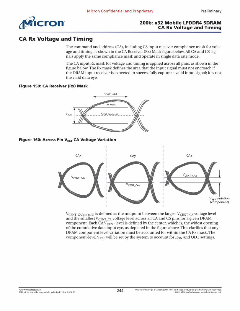
CA Rx Voltage and TimingThe command and address (CA), including CS input receiver compliance mask for volt-age and timing, is shown in the CA Receiver (Rx) Mask figure below. All CA and CS sig-nals apply the same compliance mask and operate in single data rate mode.
The CA input Rx mask for voltage and timing is applied across all pins, as shown in thefigure below. The Rx mask defines the area that the input signal must not encroach ifthe DRAM input receiver is expected to successfully capture a valid input signal; it is notthe valid data eye.
Figure 159: CA Receiver (Rx) Mask
tcIVW_total
VcIVW
Rx Mask
VCENT_CA(pin mid)
Figure 160: Across Pin VREF CA Voltage Variation
VCENT_CAx
VCENT_CAy
VCENT_CAz
CAx CAy CAz
VREF variation(component)
VCENT_CA(pin mid) is defined as the midpoint between the largest VCENT_CA voltage leveland the smallest VCENT_CA voltage level across all CA and CS pins for a given DRAMcomponent. Each CA VCENT level is defined by the center, which is, the widest openingof the cumulative data input eye, as depicted in the figure above. This clarifies that anyDRAM component level variation must be accounted for within the CA Rx mask. Thecomponent-level VREF will be set by the system to account for RON and ODT settings.
Micron Confidential and Proprietary Preliminary
200b: x32 Mobile LPDDR4 SDRAMCA Rx Voltage and Timing
PDF: 09005aef8653a92d200b_z01m_sdp_ddp_qdp_mobile_lpddr4.pdf – Rev. B 4/16 EN 244 Micron Technology, Inc. reserves the right to change products or specifications without notice.
© 2015 Micron Technology, Inc. All rights reserved.
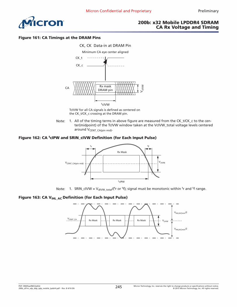
Figure 161: CA Timings at the DRAM Pins
CK, CK Data-in at DRAM Pin
Minimum CA eye center aligned
Rx maskDRAM pin
CK_c
CK_t
CA
TcIVW for all CA signals is defined as centered onthe CK_t/CK_c crossing at the DRAM pin.
VcI
VW
tcIVW
Note: 1. All of the timing terms in above figure are measured from the CK_t/CK_c to the cen-ter(midpoint) of the TcIVW window taken at the VcIVW_total voltage levels centeredaround VCENT_CA(pin mid).
Figure 162: CA tcIPW and SRIN_cIVW Definition (for Each Input Pulse)
tr tf
tcIPW
VcIVW
Rx Mask
VCENT_CA(pin mid)
Note: 1. SRIN_cIVW = VdIVW_total/(tr or tf); signal must be monotonic within tr and tf range.
Figure 163: CA VIHL_AC Definition (for Each Input Pulse)
Rx Mask Rx Mask Rx Mask
VIHL(AC)min/2
VCENT_CA VcIVW
VIHL(AC)min/2
Micron Confidential and Proprietary Preliminary
200b: x32 Mobile LPDDR4 SDRAMCA Rx Voltage and Timing
PDF: 09005aef8653a92d200b_z01m_sdp_ddp_qdp_mobile_lpddr4.pdf – Rev. B 4/16 EN 245 Micron Technology, Inc. reserves the right to change products or specifications without notice.
© 2015 Micron Technology, Inc. All rights reserved.
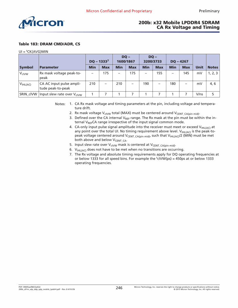
Table 183: DRAM CMD/ADR, CS
UI = tCK(AVG)MIN
Symbol Parameter
DQ – 13337DQ –
1600/1867DQ –
3200/3733 DQ – 4267
Unit NotesMin Max Min Max Min Max Min Max
VclVW Rx mask voltage peak-to-peak
– 175 – 175 – 155 – 145 mV 1, 2, 3
VIHL(AC) CA AC input pulse ampli-tude peak-to-peak
210 – 210 – 190 – 180 – mV 4, 6
SRIN_clVW Input slew rate over VclVW 1 7 1 7 1 7 1 7 V/ns 5
Notes: 1. CA Rx mask voltage and timing parameters at the pin, including voltage and tempera-ture drift.
2. Rx mask voltage VcIVW total (MAX) must be centered around VCENT_CA(pin mid).3. Defined over the CA internal VREF range. The Rx mask at the pin must be within the in-
ternal VREFCA range irrespective of the input signal common mode.4. CA-only input pulse signal amplitude into the receiver must meet or exceed VIHL(AC) at
any point over the total UI. No timing requirement above level. VIHL(AC) is the peak-to-peak voltage centered around VCENT_CA(pin mid), such that VIHL(AC)/2 (MIN) must be metboth above and below VCENT_CA.
5. Input slew rate over VcIVW mask is centered at VCENT_CA(pin mid).6. VIHL(AC) does not have to be met when no transitions are occurring.7. The Rx voltage and absolute timing requirements apply for DQ operating frequencies at
or below 1333 for all speed bins. For example the tcIVW(ps) = 450ps at or below 1333operating frequencies.
Micron Confidential and Proprietary Preliminary
200b: x32 Mobile LPDDR4 SDRAMCA Rx Voltage and Timing
PDF: 09005aef8653a92d200b_z01m_sdp_ddp_qdp_mobile_lpddr4.pdf – Rev. B 4/16 EN 246 Micron Technology, Inc. reserves the right to change products or specifications without notice.
© 2015 Micron Technology, Inc. All rights reserved.
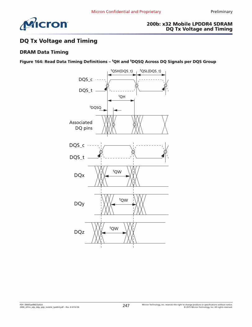
DQ Tx Voltage and Timing
DRAM Data Timing
Figure 164: Read Data Timing Definitions – tQH and tDQSQ Across DQ Signals per DQS Group
DQS_t
DQS_c
tQSH(DQS_t)
tQH
tDQSQ
tQSL(DQS_t)
AssociatedDQ pins
DQS_t
DQS_c
tQWDQx
tQWDQy
tQWDQz
Micron Confidential and Proprietary Preliminary
200b: x32 Mobile LPDDR4 SDRAMDQ Tx Voltage and Timing
PDF: 09005aef8653a92d200b_z01m_sdp_ddp_qdp_mobile_lpddr4.pdf – Rev. B 4/16 EN 247 Micron Technology, Inc. reserves the right to change products or specifications without notice.
© 2015 Micron Technology, Inc. All rights reserved.
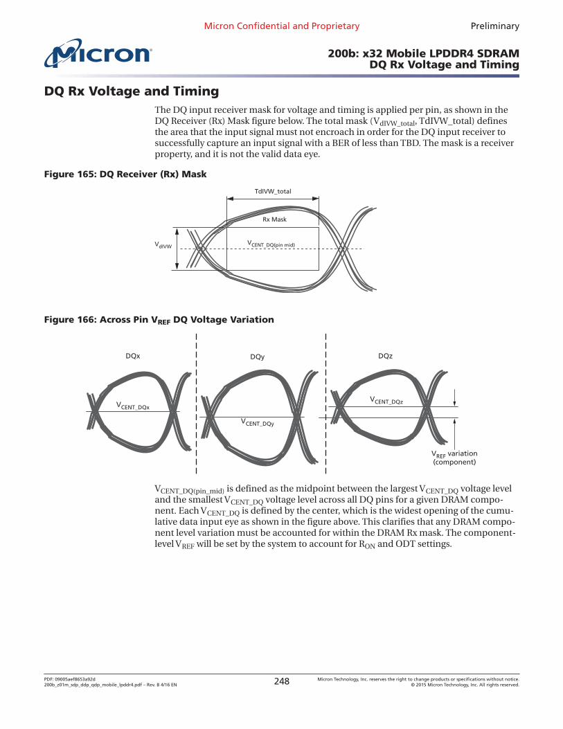
DQ Rx Voltage and TimingThe DQ input receiver mask for voltage and timing is applied per pin, as shown in theDQ Receiver (Rx) Mask figure below. The total mask (VdIVW_total, TdIVW_total) definesthe area that the input signal must not encroach in order for the DQ input receiver tosuccessfully capture an input signal with a BER of less than TBD. The mask is a receiverproperty, and it is not the valid data eye.
Figure 165: DQ Receiver (Rx) Mask
TdIVW_total
VdIVW
Rx Mask
VCENT_DQ(pin mid)
Figure 166: Across Pin VREF DQ Voltage Variation
VCENT_DQx
VCENT_DQy
VCENT_DQz
DQx DQy DQz
VREF variation(component)
VCENT_DQ(pin_mid) is defined as the midpoint between the largest VCENT_DQ voltage leveland the smallest VCENT_DQ voltage level across all DQ pins for a given DRAM compo-nent. Each VCENT_DQ is defined by the center, which is the widest opening of the cumu-lative data input eye as shown in the figure above. This clarifies that any DRAM compo-nent level variation must be accounted for within the DRAM Rx mask. The component-level VREF will be set by the system to account for RON and ODT settings.
Micron Confidential and Proprietary Preliminary
200b: x32 Mobile LPDDR4 SDRAMDQ Rx Voltage and Timing
PDF: 09005aef8653a92d200b_z01m_sdp_ddp_qdp_mobile_lpddr4.pdf – Rev. B 4/16 EN 248 Micron Technology, Inc. reserves the right to change products or specifications without notice.
© 2015 Micron Technology, Inc. All rights reserved.
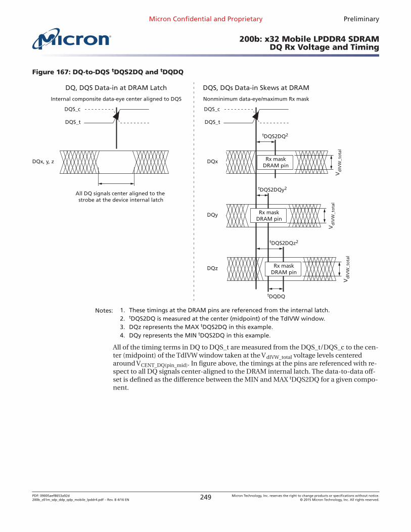
Figure 167: DQ-to-DQS tDQS2DQ and tDQDQ
DQS, DQs Data-in Skews at DRAMDQ, DQS Data-in at DRAM Latch
Internal componsite data-eye center aligned to DQS Nonminimum data-eye/maximum Rx mask
DQS_t
DQS_c
DQx, y, z DQx
DQS_t
DQS_c
Vd
IVW
_to
tal
tDQS2DQ2
All DQ signals center aligned to the strobe at the device internal latch
Rx maskDRAM pin
Vd
IVW
_to
tal
tDQS2DQy2
Rx maskDRAM pin
DQz
Vd
IVW
_to
tal
tDQS2DQz2
tDQDQ
Rx maskDRAM pin
DQy
Notes: 1. These timings at the DRAM pins are referenced from the internal latch.2. tDQS2DQ is measured at the center (midpoint) of the TdIVW window.3. DQz represents the MAX tDQS2DQ in this example.4. DQy represents the MIN tDQS2DQ in this example.
All of the timing terms in DQ to DQS_t are measured from the DQS_t/DQS_c to the cen-ter (midpoint) of the TdIVW window taken at the VdIVW_total voltage levels centeredaround VCENT_DQ(pin_mid). In figure above, the timings at the pins are referenced with re-spect to all DQ signals center-aligned to the DRAM internal latch. The data-to-data off-set is defined as the difference between the MIN and MAX tDQS2DQ for a given compo-nent.
Micron Confidential and Proprietary Preliminary
200b: x32 Mobile LPDDR4 SDRAMDQ Rx Voltage and Timing
PDF: 09005aef8653a92d200b_z01m_sdp_ddp_qdp_mobile_lpddr4.pdf – Rev. B 4/16 EN 249 Micron Technology, Inc. reserves the right to change products or specifications without notice.
© 2015 Micron Technology, Inc. All rights reserved.
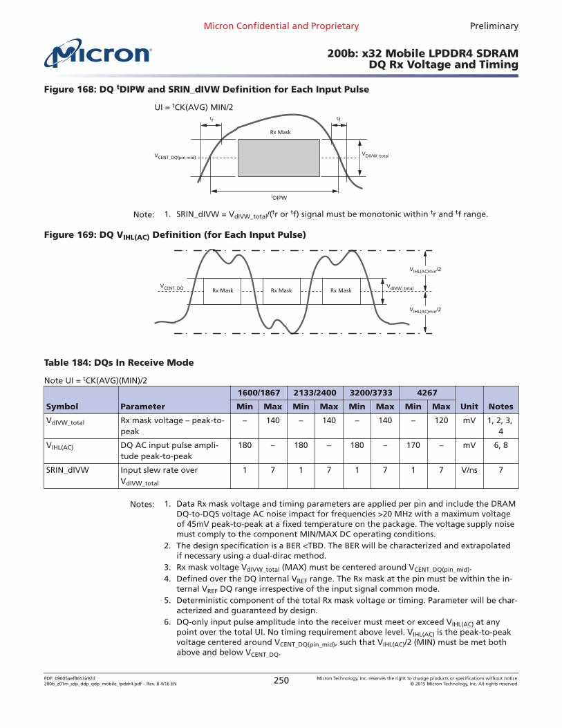
Figure 168: DQ tDIPW and SRIN_dIVW Definition for Each Input Pulse
UI = tCK(AVG) MIN/2tr tf
tDIPW
VDIVW_total
Rx Mask
VCENT_DQ(pin mid)
Note: 1. SRIN_dIVW = VdIVW_total/(tr or tf) signal must be monotonic within tr and tf range.
Figure 169: DQ VIHL(AC) Definition (for Each Input Pulse)
Rx Mask Rx Mask Rx Mask
VIHL(AC)min/2
VIHL(AC)min/2
VdIVW_totalVCENT_DQ
Table 184: DQs In Receive Mode
Note UI = tCK(AVG)(MIN)/2
Symbol Parameter
1600/1867 2133/2400 3200/3733 4267
Unit NotesMin Max Min Max Min Max Min Max
VdIVW_total Rx mask voltage – peak-to-peak
– 140 – 140 – 140 – 120 mV 1, 2, 3, 4
VIHL(AC) DQ AC input pulse ampli-tude peak-to-peak
180 – 180 – 180 – 170 – mV 6, 8
SRIN_dIVW Input slew rate overVdIVW_total
1 7 1 7 1 7 1 7 V/ns 7
Notes: 1. Data Rx mask voltage and timing parameters are applied per pin and include the DRAMDQ-to-DQS voltage AC noise impact for frequencies >20 MHz with a maximum voltageof 45mV peak-to-peak at a fixed temperature on the package. The voltage supply noisemust comply to the component MIN/MAX DC operating conditions.
2. The design specification is a BER <TBD. The BER will be characterized and extrapolatedif necessary using a dual-dirac method.
3. Rx mask voltage VdIVW_total (MAX) must be centered around VCENT_DQ(pin_mid).4. Defined over the DQ internal VREF range. The Rx mask at the pin must be within the in-
ternal VREF DQ range irrespective of the input signal common mode.5. Deterministic component of the total Rx mask voltage or timing. Parameter will be char-
acterized and guaranteed by design.6. DQ-only input pulse amplitude into the receiver must meet or exceed VIHL(AC) at any
point over the total UI. No timing requirement above level. VIHL(AC) is the peak-to-peakvoltage centered around VCENT_DQ(pin_mid), such that VIHL(AC)/2 (MIN) must be met bothabove and below VCENT_DQ.
Micron Confidential and Proprietary Preliminary
200b: x32 Mobile LPDDR4 SDRAMDQ Rx Voltage and Timing
PDF: 09005aef8653a92d200b_z01m_sdp_ddp_qdp_mobile_lpddr4.pdf – Rev. B 4/16 EN 250 Micron Technology, Inc. reserves the right to change products or specifications without notice.
© 2015 Micron Technology, Inc. All rights reserved.
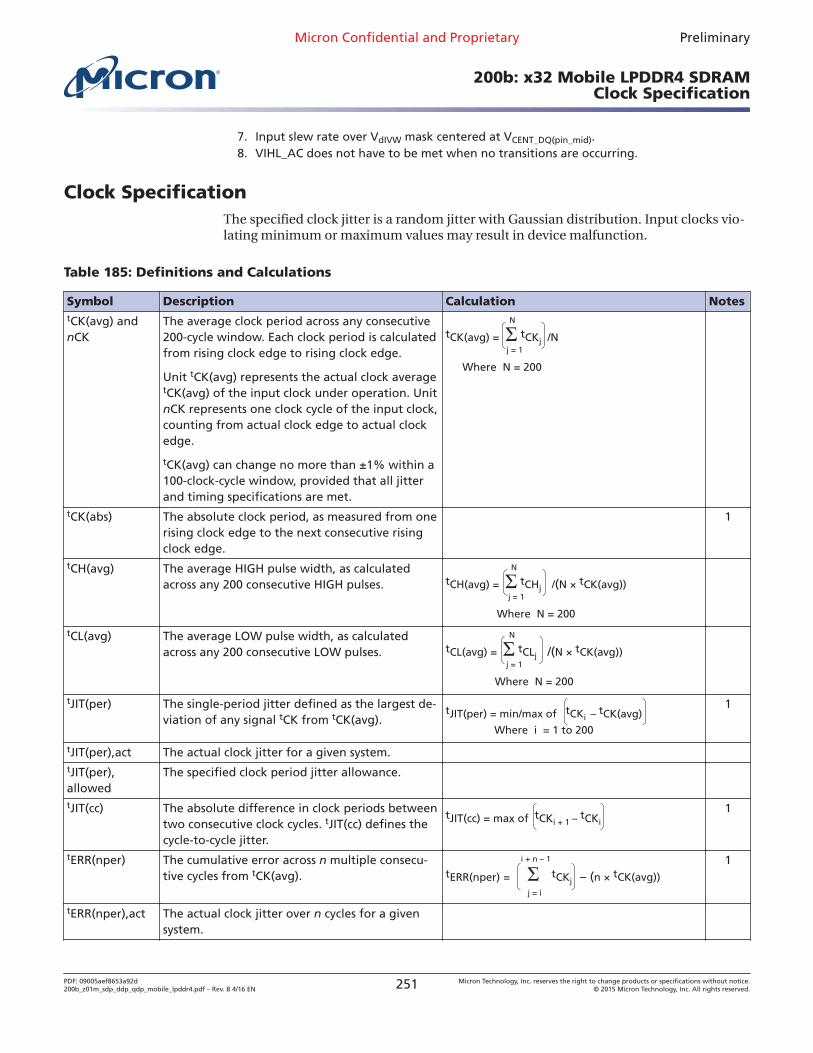
7. Input slew rate over VdIVW mask centered at VCENT_DQ(pin_mid).8. VIHL_AC does not have to be met when no transitions are occurring.
Clock SpecificationThe specified clock jitter is a random jitter with Gaussian distribution. Input clocks vio-lating minimum or maximum values may result in device malfunction.
Table 185: Definitions and Calculations
Symbol Description Calculation NotestCK(avg) andnCK
The average clock period across any consecutive200-cycle window. Each clock period is calculatedfrom rising clock edge to rising clock edge.
Unit tCK(avg) represents the actual clock averagetCK(avg) of the input clock under operation. UnitnCK represents one clock cycle of the input clock,counting from actual clock edge to actual clockedge.
tCK(avg) can change no more than ±1% within a100-clock-cycle window, provided that all jitterand timing specifications are met.
tCK(avg) = Σ tCKj /N
Where N = 200
N
j = 1
tCK(abs) The absolute clock period, as measured from onerising clock edge to the next consecutive risingclock edge.
1
tCH(avg) The average HIGH pulse width, as calculatedacross any 200 consecutive HIGH pulses. tCH(avg) = Σ tCHj /(N × tCK(avg))
Where N = 200
N
j = 1
tCL(avg) The average LOW pulse width, as calculatedacross any 200 consecutive LOW pulses. tCL(avg) = Σ tCLj /(N × tCK(avg))
Where N = 200
N
j = 1
tJIT(per) The single-period jitter defined as the largest de-viation of any signal tCK from tCK(avg).
tJIT(per) = min/max of tCKi – tCK(avg)
Where i = 1 to 200
1
tJIT(per),act The actual clock jitter for a given system. tJIT(per),allowed
The specified clock period jitter allowance.
tJIT(cc) The absolute difference in clock periods betweentwo consecutive clock cycles. tJIT(cc) defines thecycle-to-cycle jitter.
tJIT(cc) = max of tCKi + 1 – tCKi
1
tERR(nper) The cumulative error across n multiple consecu-tive cycles from tCK(avg). tERR(nper) = Σ tCKj – (n × tCK(avg))
i + n – 1
j = i
1
tERR(nper),act The actual clock jitter over n cycles for a givensystem.
Micron Confidential and Proprietary Preliminary
200b: x32 Mobile LPDDR4 SDRAMClock Specification
PDF: 09005aef8653a92d200b_z01m_sdp_ddp_qdp_mobile_lpddr4.pdf – Rev. B 4/16 EN 251 Micron Technology, Inc. reserves the right to change products or specifications without notice.
© 2015 Micron Technology, Inc. All rights reserved.
Table 185: Definitions and Calculations (Continued)
Symbol Description Calculation NotestERR(nper),allowed
The specified clock jitter allowance over n cycles.
tERR(nper),min The minimum tERR(nper). tERR(nper),min = (1 + 0.68LN(n)) × tJIT(per),min 2
tERR(nper),max The maximum tERR(nper). tERR(nper),max = (1 + 0.68LN(n)) × tJIT(per),max 2
tJIT(duty) Defined with absolute and average specificationsfor tCH and tCL, respectively.
tJIT(duty),min = MIN((tCH(abs),min – tCH(avg),min), (tCL(abs),min – tCL(avg),min)) × tCK(avg) tJIT(duty),max = MAX((tCH(abs),max – tCH(avg),max), (tCL(abs),max – tCL(avg),max)) × tCK(avg)
Notes: 1. Not subject to production testing.2. Using these equations, tERR(nper) tables can be generated for each tJIT(per),act value.
tCK(abs), tCH(abs), and tCL(abs)
These parameters are specified with their average values; however, the relationship be-tween the average timing and the absolute instantaneous timing (defined in the follow-ing table) is applicable at all times.
Table 186: tCK(abs), tCH(abs), and tCL(abs) Definitions
Parameter Symbol Minimum Unit
Absolute clock period tCK(abs) tCK(avg),min + tJIT(per),min ps1
Absolute clock HIGH pulse width tCH(abs) tCH(avg),min + tJIT(duty),min2/tCK(avg)min tCK(avg)
Absolute clock LOW pulse width tCL(abs) tCL(avg),min + tJIT(duty),min2/tCK(avg)min tCK(avg)
Notes: 1. tCK(avg),min is expressed in ps for this table.2. tJIT(duty),min is a negative value.
Clock Period JitterLPDDR4 devices can tolerate some clock period jitter without core timing parameterderating. This section describes device timing requirements with clock period jitter(tJIT(per)) in excess of the values found in the AC Timing table. Calculating cycle timederating and clock cycle derating are also described.
Clock Period Jitter Effects on Core Timing Parameters
Core timing parameters (tRCD, tRP, tRTP, tWR, tWRA, tWTR, tRC, tRAS, tRRD, tFAW) ex-tend across multiple clock cycles. Clock period jitter impacts these parameters whenmeasured in numbers of clock cycles. Within the specification limits, the device is char-acterized and verified to support tnPARAM = RU[tPARAM/tCK(avg)]. During device op-eration where clock jitter is outside specification limits, the number of clocks, ortCK(avg), may need to be increased based on the values for each core timing parameter.
Micron Confidential and Proprietary Preliminary
200b: x32 Mobile LPDDR4 SDRAMClock Period Jitter
PDF: 09005aef8653a92d200b_z01m_sdp_ddp_qdp_mobile_lpddr4.pdf – Rev. B 4/16 EN 252 Micron Technology, Inc. reserves the right to change products or specifications without notice.
© 2015 Micron Technology, Inc. All rights reserved.
Cycle Time Derating for Core Timing Parameters
For a given number of clocks (tnPARAM), when tCK(avg) and tERR(tnPARAM),act exceedtERR(tnPARAM),allowed, cycle time derating may be required for core timing parame-ters.
CycleTimeDerating = max tPARAM + tERR(tnPARAM),act – tERR(tnPARAM),allowed – tCK(avg) , 0
tnPARAM
Cycle time derating analysis should be conducted for each core timing parameter. Theamount of cycle time derating required is the maximum of the cycle time deratings de-termined for each individual core timing parameter.
Clock Cycle Derating for Core Timing Parameters
For each core timing parameter and a given number of clocks (tnPARAM), clock cyclederating should be specified with tJIT(per).
For a given number of clocks (tnPARAM), when tCK(avg) plus (tERR(tnPARAM),act) ex-ceed the supported cumulative tERR(tnPARAM),allowed, derating is required. If theequation below results in a positive value for a core timing parameter (tCORE), the re-quired clock cycle derating will be that positive value (in clocks).
ClockCycleDerating = RU tPARAM + tERR(tnPARAM),act – tERR(tnPARAM),allowed – tnPARAM
tCK(avg)
Cycle-time derating analysis should be conducted for each core timing parameter.
Clock Jitter Effects on Command/Address Timing Parameters
Command/address timing parameters (tIS, tIH, tISb, tIHb) are measured from a com-mand/address signal (CS or CA[5:0]) transition edge to its respective clock signal (CK_t/CK_c) crossing. The specification values are not affected by the tJIT(per) applied, be-cause the setup and hold times are relative to the clock signal crossing that latches thecommand/address. Regardless of clock jitter values, these values must be met.
Clock Jitter Effects on READ Timing ParameterstRPRE
When the device is operated with input clock jitter, tRPRE must be derated by thetJIT(per),act,max of the input clock that exceeds tJIT(per),allowed,max. Output derat-ings are relative to the input clock:
tRPRE(min,derated) = 0.9 – tJIT(per),act,max – tJIT(per),allowed,max
tCK(avg)
For example, if the measured jitter into a LPDDR4 device has tCK(avg) = 625ps,tJIT(per),act,min = –xx, and tJIT(per),act,max = +xx ps, then tRPRE,min,derated = 0.9 -(tJIT(per),act,max - tJIT(per),allowed,max)/tCK(avg) = 0.9 - (xx - xx)/xx = yy tCK(avg).
Micron Confidential and Proprietary Preliminary
200b: x32 Mobile LPDDR4 SDRAMClock Period Jitter
PDF: 09005aef8653a92d200b_z01m_sdp_ddp_qdp_mobile_lpddr4.pdf – Rev. B 4/16 EN 253 Micron Technology, Inc. reserves the right to change products or specifications without notice.
© 2015 Micron Technology, Inc. All rights reserved.
tLZ(DQ), tHZ(DQ), tDQSCK, tLZ(DQS), tHZ(DQS)
These parameters are measured from a specific clock edge to a data signal transition(DMn or DQm, where: n = 0,1; and m = 0–15, and specified timings must be met withrespect to that clock edge. Therefore, they are not affected by tJIT(per).
tQSH, tQSL
These parameters are affected by duty cycle jitter, represented by tCH(abs)min andtCL(abs)min. These parameters determine the absolute data-valid window at the devicepin. The absolute minimum data-valid window at the device pin = MIN {(tQSH(abs)min- tDQSQmax), (tQSL(abs)min - tDQSQmax)}. This minimum data valid window must bemet at the target frequency regardless of clock jitter.
tRPST
tRPST is affected by duty cycle jitter, represented by tCL(abs). Therefore, tRPST(abs)mincan be specified by tCL(abs)min. tRPST(abs)min = tCL(abs)min - 0.05 = tQSL(abs)min.
Clock Jitter Effects on WRITE Timing ParameterstDS, tDH
These parameters are measured from a data signal (DMIn or DQm, where n = 0, 1 and m= 0–15) transition edge to its respective data strobe signal (DQSn_t, DQSn_c: n = 0,1)crossing. The specification values are not affected by the amount of tJIT(per) applied,because the setup and hold times are relative to the data strobe signal crossing thatlatches the command/address. Regardless of clock jitter values, these values must bemet.
tDSS, tDSH
These parameters are measured from a data signal (DQS_t, DQSn_c) crossing to its re-spective clock signal (CK_t, CK_c) crossing. When the device is operated with inputclock jitter, this parameter needs to be derated by the actual tJIT(per)act of the input clockin excess of the allowed period jitter tJIT(per)allowed.
tDQSS
tDQSS is measured from a data strobe signal (DQSn_t, DQSn_c) crossing to its respec-tive clock signal (CK_t, CK_c) crossing. When the device is operated with input clock jit-ter, this parameter must be derated by the actual tJIT(per),act of the input clock in ex-cess of tJIT(per)allowed.
tDQSS(min,derated) = 0.75 - tJIT(per),act,min – tJIT(per),allowed, min
tCK(avg)
tDQSS(max,derated) = 1.25 – tJIT(per),act,max – tJIT(per),allowed, max
tCK(avg)
For example, if the measured jitter into an LPDDR4 device has tCK(avg) = 625ps,tJIT(per),act,min = -xxps, and tJIT(per),act,max = +xx ps, then:
tDQSS,(min,derated) = 0.75 - (-xx + yy)/625 = xxxx tCK(avg)
tDQSS,(max,derated) = 1.25 - (xx – yy)/625 = xxxx tCK(avg)
Micron Confidential and Proprietary Preliminary
200b: x32 Mobile LPDDR4 SDRAMClock Period Jitter
PDF: 09005aef8653a92d200b_z01m_sdp_ddp_qdp_mobile_lpddr4.pdf – Rev. B 4/16 EN 254 Micron Technology, Inc. reserves the right to change products or specifications without notice.
© 2015 Micron Technology, Inc. All rights reserved.
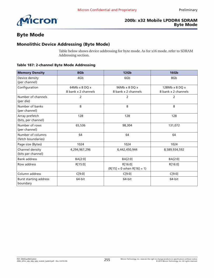
Byte Mode
Monolithic Device Addressing (Byte Mode)
Table below shows device addressing for byte mode. As for x16 mode, refer to SDRAMAddressing section.
Table 187: 2-channel Byte Mode Addressing
Memory Density 8Gb 12Gb 16Gb
Device density(per channel)
4Gb 6Gb 8Gb
Configuration 64Mb x 8 DQ x8 bank x 2 channels
96Mb x 8 DQ x8 bank x 2 channels
128Mb x 8 DQ x8 bank x 2 channels
Number of channels(per die)
2 2 2
Number of banks(per channel)
8 8 8
Array prefetch(bits, per channel)
128 128 128
Number of rows(per channel)
65,536 98,304 131,072
Number of columns(fetch boundaries)
64 64 64
Page size (Bytes) 1024 1024 1024
Channel density(bits per channel)
4,294,967,296 6,442,450,944 8,589,934,592
Bank address BA[2:0] BA[2:0] BA[2:0]
Row address R[15:0] R[16:0](R[15] = 0 when R[16] = 1)
R[16:0]
Column address C[9:0] C[9:0] C[9:0]
Burst starting addressboundary
64-bit 64-bit 64-bit
Micron Confidential and Proprietary Preliminary
200b: x32 Mobile LPDDR4 SDRAMByte Mode
PDF: 09005aef8653a92d200b_z01m_sdp_ddp_qdp_mobile_lpddr4.pdf – Rev. B 4/16 EN 255 Micron Technology, Inc. reserves the right to change products or specifications without notice.
© 2015 Micron Technology, Inc. All rights reserved.
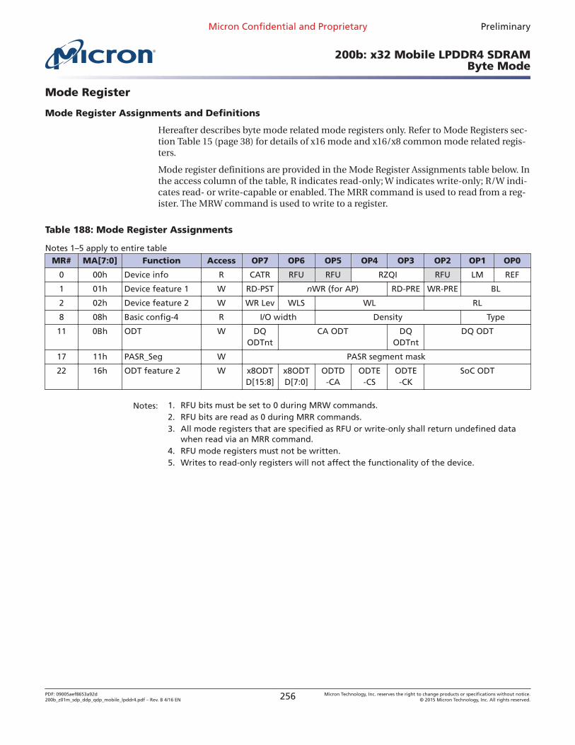
Mode Register
Mode Register Assignments and Definitions
Hereafter describes byte mode related mode registers only. Refer to Mode Registers sec-tion Table 15 (page 38) for details of x16 mode and x16/x8 common mode related regis-ters.
Mode register definitions are provided in the Mode Register Assignments table below. Inthe access column of the table, R indicates read-only; W indicates write-only; R/W indi-cates read- or write-capable or enabled. The MRR command is used to read from a reg-ister. The MRW command is used to write to a register.
Table 188: Mode Register Assignments
Notes 1–5 apply to entire tableMR# MA[7:0] Function Access OP7 OP6 OP5 OP4 OP3 OP2 OP1 OP0
0 00h Device info R CATR RFU RFU RZQI RFU LM REF
1 01h Device feature 1 W RD-PST nWR (for AP) RD-PRE WR-PRE BL
2 02h Device feature 2 W WR Lev WLS WL RL
8 08h Basic config-4 R I/O width Density Type
11 0Bh ODT W DQODTnt
CA ODT DQODTnt
DQ ODT
17 11h PASR_Seg W PASR segment mask
22 16h ODT feature 2 W x8ODTD[15:8]
x8ODTD[7:0]
ODTD-CA
ODTE-CS
ODTE-CK
SoC ODT
Notes: 1. RFU bits must be set to 0 during MRW commands.2. RFU bits are read as 0 during MRR commands.3. All mode registers that are specified as RFU or write-only shall return undefined data
when read via an MRR command.4. RFU mode registers must not be written.5. Writes to read-only registers will not affect the functionality of the device.
Micron Confidential and Proprietary Preliminary
200b: x32 Mobile LPDDR4 SDRAMByte Mode
PDF: 09005aef8653a92d200b_z01m_sdp_ddp_qdp_mobile_lpddr4.pdf – Rev. B 4/16 EN 256 Micron Technology, Inc. reserves the right to change products or specifications without notice.
© 2015 Micron Technology, Inc. All rights reserved.
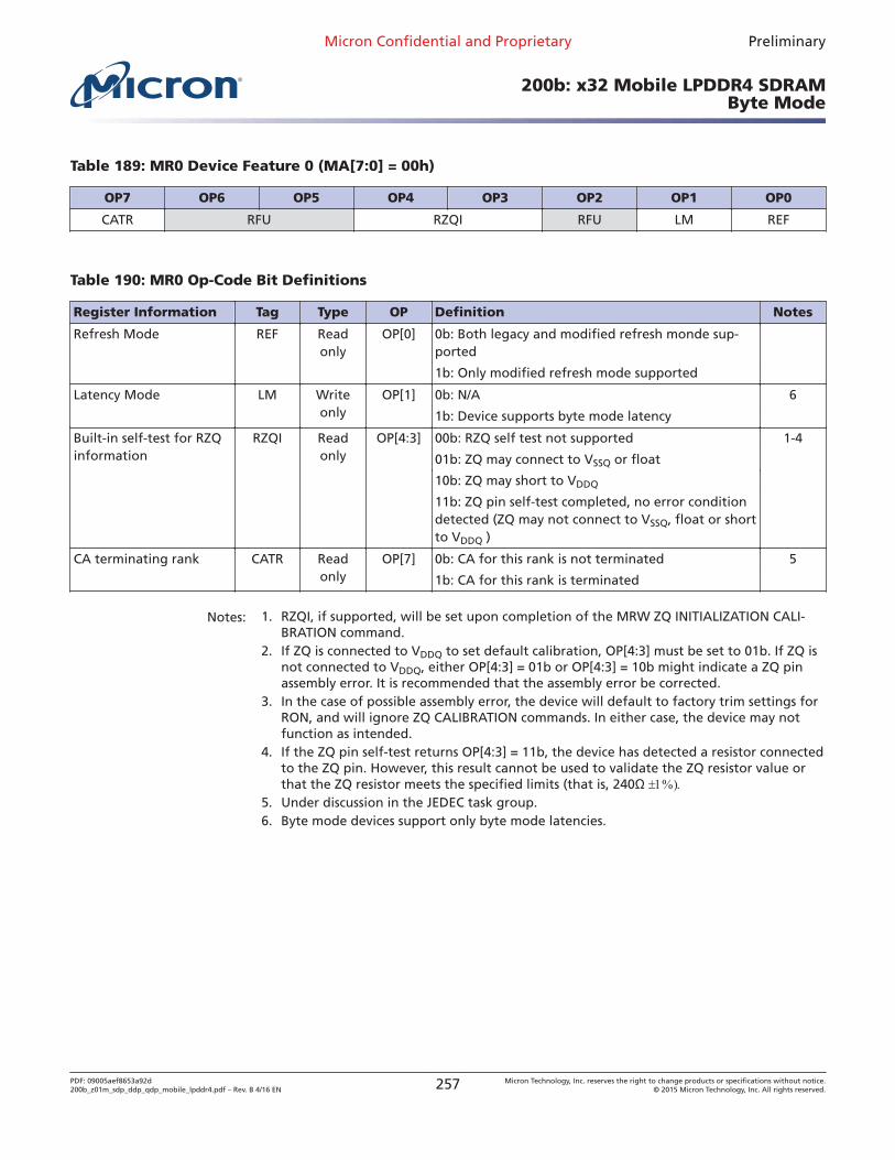
Table 189: MR0 Device Feature 0 (MA[7:0] = 00h)
OP7 OP6 OP5 OP4 OP3 OP2 OP1 OP0
CATR RFU RZQI RFU LM REF
Table 190: MR0 Op-Code Bit Definitions
Register Information Tag Type OP Definition Notes
Refresh Mode REF Readonly
OP[0] 0b: Both legacy and modified refresh monde sup-ported
1b: Only modified refresh mode supported
Latency Mode LM Writeonly
OP[1] 0b: N/A 6
1b: Device supports byte mode latency
Built-in self-test for RZQinformation
RZQI Readonly
OP[4:3] 00b: RZQ self test not supported 1-4
01b: ZQ may connect to VSSQ or float
10b: ZQ may short to VDDQ
11b: ZQ pin self-test completed, no error conditiondetected (ZQ may not connect to VSSQ, float or shortto VDDQ )
CA terminating rank CATR Readonly
OP[7] 0b: CA for this rank is not terminated 5
1b: CA for this rank is terminated
Notes: 1. RZQI, if supported, will be set upon completion of the MRW ZQ INITIALIZATION CALI-BRATION command.
2. If ZQ is connected to VDDQ to set default calibration, OP[4:3] must be set to 01b. If ZQ isnot connected to VDDQ, either OP[4:3] = 01b or OP[4:3] = 10b might indicate a ZQ pinassembly error. It is recommended that the assembly error be corrected.
3. In the case of possible assembly error, the device will default to factory trim settings forRON, and will ignore ZQ CALIBRATION commands. In either case, the device may notfunction as intended.
4. If the ZQ pin self-test returns OP[4:3] = 11b, the device has detected a resistor connectedto the ZQ pin. However, this result cannot be used to validate the ZQ resistor value orthat the ZQ resistor meets the specified limits (that is, 240Ω
5. Under discussion in the JEDEC task group.6. Byte mode devices support only byte mode latencies.
Micron Confidential and Proprietary Preliminary
200b: x32 Mobile LPDDR4 SDRAMByte Mode
PDF: 09005aef8653a92d200b_z01m_sdp_ddp_qdp_mobile_lpddr4.pdf – Rev. B 4/16 EN 257 Micron Technology, Inc. reserves the right to change products or specifications without notice.
© 2015 Micron Technology, Inc. All rights reserved.
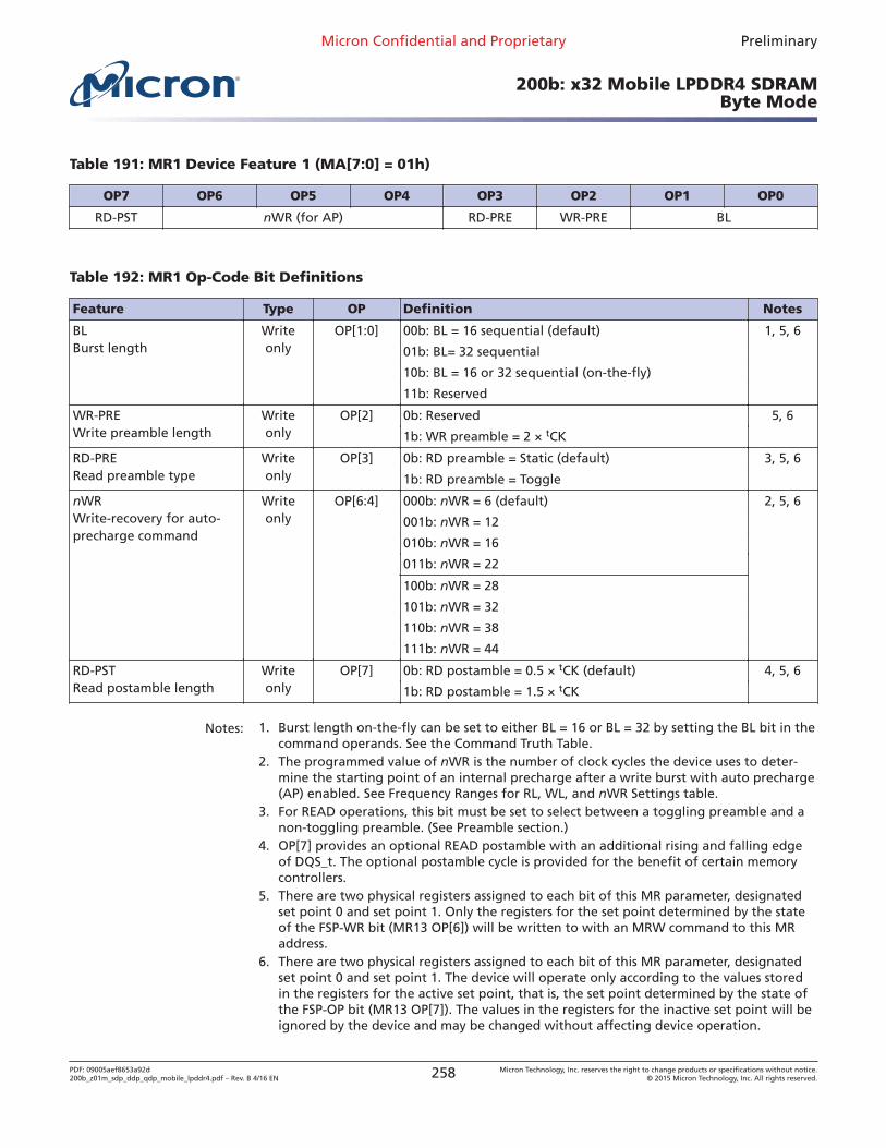
Table 191: MR1 Device Feature 1 (MA[7:0] = 01h)
OP7 OP6 OP5 OP4 OP3 OP2 OP1 OP0
RD-PST nWR (for AP) RD-PRE WR-PRE BL
Table 192: MR1 Op-Code Bit Definitions
Feature Type OP Definition Notes
BLBurst length
Writeonly
OP[1:0] 00b: BL = 16 sequential (default) 1, 5, 6
01b: BL= 32 sequential
10b: BL = 16 or 32 sequential (on-the-fly)
11b: Reserved
WR-PREWrite preamble length
Writeonly
OP[2] 0b: Reserved 5, 6
1b: WR preamble = 2 × tCK
RD-PRERead preamble type
Writeonly
OP[3] 0b: RD preamble = Static (default) 3, 5, 6
1b: RD preamble = Toggle
nWRWrite-recovery for auto-precharge command
Writeonly
OP[6:4] 000b: nWR = 6 (default) 2, 5, 6
001b: nWR = 12
010b: nWR = 16
011b: nWR = 22
100b: nWR = 28
101b: nWR = 32
110b: nWR = 38
111b: nWR = 44
RD-PSTRead postamble length
Writeonly
OP[7] 0b: RD postamble = 0.5 × tCK (default) 4, 5, 6
1b: RD postamble = 1.5 × tCK
Notes: 1. Burst length on-the-fly can be set to either BL = 16 or BL = 32 by setting the BL bit in thecommand operands. See the Command Truth Table.
2. The programmed value of nWR is the number of clock cycles the device uses to deter-mine the starting point of an internal precharge after a write burst with auto precharge(AP) enabled. See Frequency Ranges for RL, WL, and nWR Settings table.
3. For READ operations, this bit must be set to select between a toggling preamble and anon-toggling preamble. (See Preamble section.)
4. OP[7] provides an optional READ postamble with an additional rising and falling edgeof DQS_t. The optional postamble cycle is provided for the benefit of certain memorycontrollers.
5. There are two physical registers assigned to each bit of this MR parameter, designatedset point 0 and set point 1. Only the registers for the set point determined by the stateof the FSP‐WR bit (MR13 OP[6]) will be written to with an MRW command to this MRaddress.
6. There are two physical registers assigned to each bit of this MR parameter, designatedset point 0 and set point 1. The device will operate only according to the values storedin the registers for the active set point, that is, the set point determined by the state ofthe FSP‐OP bit (MR13 OP[7]). The values in the registers for the inactive set point will beignored by the device and may be changed without affecting device operation.
Micron Confidential and Proprietary Preliminary
200b: x32 Mobile LPDDR4 SDRAMByte Mode
PDF: 09005aef8653a92d200b_z01m_sdp_ddp_qdp_mobile_lpddr4.pdf – Rev. B 4/16 EN 258 Micron Technology, Inc. reserves the right to change products or specifications without notice.
© 2015 Micron Technology, Inc. All rights reserved.
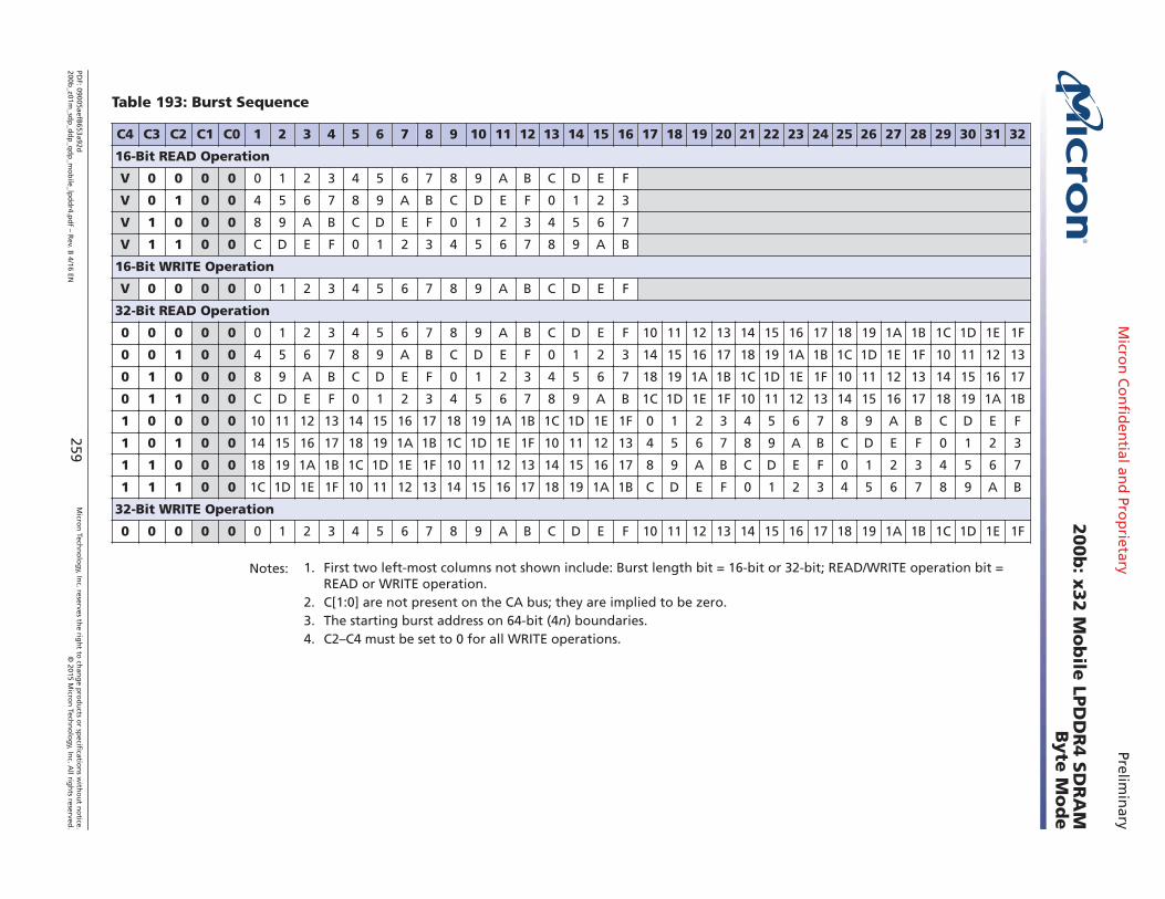
Table 193: Burst Sequence
C4 C3 C2 C1 C0 1 2 3 4 5 6 7 8 9 10 11 12 13 14 15 16 17 18 19 20 21 22 23 24 25 26 27 28 29 30 31 32
16-Bit READ Operation
V 0 0 0 0 0 1 2 3 4 5 6 7 8 9 A B C D E F
V 0 1 0 0 4 5 6 7 8 9 A B C D E F 0 1 2 3
V 1 0 0 0 8 9 A B C D E F 0 1 2 3 4 5 6 7
V 1 1 0 0 C D E F 0 1 2 3 4 5 6 7 8 9 A B
16-Bit WRITE Operation
V 0 0 0 0 0 1 2 3 4 5 6 7 8 9 A B C D E F
32-Bit READ Operation
0 0 0 0 0 0 1 2 3 4 5 6 7 8 9 A B C D E F 10 11 12 13 14 15 16 17 18 19 1A 1B 1C 1D 1E 1F
0 0 1 0 0 4 5 6 7 8 9 A B C D E F 0 1 2 3 14 15 16 17 18 19 1A 1B 1C 1D 1E 1F 10 11 12 13
0 1 0 0 0 8 9 A B C D E F 0 1 2 3 4 5 6 7 18 19 1A 1B 1C 1D 1E 1F 10 11 12 13 14 15 16 17
0 1 1 0 0 C D E F 0 1 2 3 4 5 6 7 8 9 A B 1C 1D 1E 1F 10 11 12 13 14 15 16 17 18 19 1A 1B
1 0 0 0 0 10 11 12 13 14 15 16 17 18 19 1A 1B 1C 1D 1E 1F 0 1 2 3 4 5 6 7 8 9 A B C D E F
1 0 1 0 0 14 15 16 17 18 19 1A 1B 1C 1D 1E 1F 10 11 12 13 4 5 6 7 8 9 A B C D E F 0 1 2 3
1 1 0 0 0 18 19 1A 1B 1C 1D 1E 1F 10 11 12 13 14 15 16 17 8 9 A B C D E F 0 1 2 3 4 5 6 7
1 1 1 0 0 1C 1D 1E 1F 10 11 12 13 14 15 16 17 18 19 1A 1B C D E F 0 1 2 3 4 5 6 7 8 9 A B
32-Bit WRITE Operation
0 0 0 0 0 0 1 2 3 4 5 6 7 8 9 A B C D E F 10 11 12 13 14 15 16 17 18 19 1A 1B 1C 1D 1E 1F
Notes: 1. First two left-most columns not shown include: Burst length bit = 16-bit or 32-bit; READ/WRITE operation bit =READ or WRITE operation.
2. C[1:0] are not present on the CA bus; they are implied to be zero.3. The starting burst address on 64-bit (4n) boundaries.4. C2–C4 must be set to 0 for all WRITE operations.
Micro
n C
on
fiden
tial and
Prop
rietaryPrelim
inary
200b
: x32 M
ob
ile LP
DD
R4 S
DR
AM
Byte
Mo
de
PDF: 09005aef8653a92d
200b_z01m
_sdp
_dd
p_q
dp
_mo
bile_lp
dd
r4.pd
f – Rev. B
4/16 EN259
Micro
n Tech
no
log
y, Inc. reserves th
e righ
t to ch
ang
e pro
du
cts or sp
ecification
s with
ou
t no
tice.©
2015 Micro
n Tech
no
log
y, Inc. A
ll righ
ts reserved.
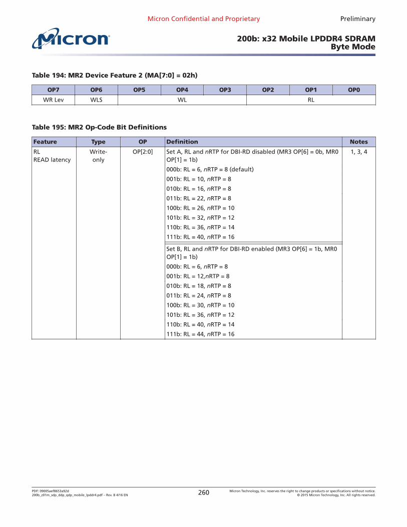
Table 194: MR2 Device Feature 2 (MA[7:0] = 02h)
OP7 OP6 OP5 OP4 OP3 OP2 OP1 OP0
WR Lev WLS WL RL
Table 195: MR2 Op-Code Bit Definitions
Feature Type OP Definition Notes
RLREAD latency
Write-only
OP[2:0] Set A, RL and nRTP for DBI-RD disabled (MR3 OP[6] = 0b, MR0OP[1] = 1b)
1, 3, 4
000b: RL = 6, nRTP = 8 (default)
001b: RL = 10, nRTP = 8
010b: RL = 16, nRTP = 8
011b: RL = 22, nRTP = 8
100b: RL = 26, nRTP = 10
101b: RL = 32, nRTP = 12
110b: RL = 36, nRTP = 14
111b: RL = 40, nRTP = 16
Set B, RL and nRTP for DBI-RD enabled (MR3 OP[6] = 1b, MR0OP[1] = 1b)
000b: RL = 6, nRTP = 8
001b: RL = 12,nRTP = 8
010b: RL = 18, nRTP = 8
011b: RL = 24, nRTP = 8
100b: RL = 30, nRTP = 10
101b: RL = 36, nRTP = 12
110b: RL = 40, nRTP = 14
111b: RL = 44, nRTP = 16
Micron Confidential and Proprietary Preliminary
200b: x32 Mobile LPDDR4 SDRAMByte Mode
PDF: 09005aef8653a92d200b_z01m_sdp_ddp_qdp_mobile_lpddr4.pdf – Rev. B 4/16 EN 260 Micron Technology, Inc. reserves the right to change products or specifications without notice.
© 2015 Micron Technology, Inc. All rights reserved.
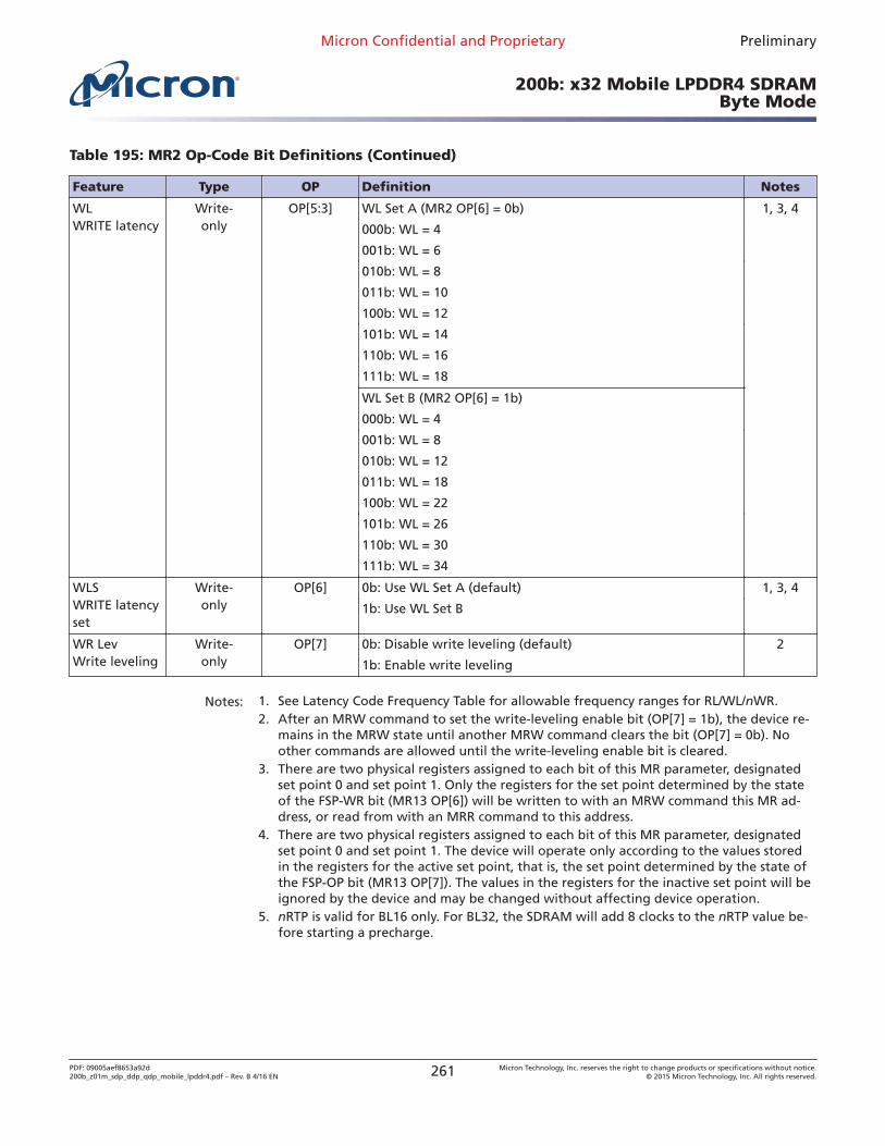
Table 195: MR2 Op-Code Bit Definitions (Continued)
Feature Type OP Definition Notes
WLWRITE latency
Write-only
OP[5:3] WL Set A (MR2 OP[6] = 0b) 1, 3, 4
000b: WL = 4
001b: WL = 6
010b: WL = 8
011b: WL = 10
100b: WL = 12
101b: WL = 14
110b: WL = 16
111b: WL = 18
WL Set B (MR2 OP[6] = 1b)
000b: WL = 4
001b: WL = 8
010b: WL = 12
011b: WL = 18
100b: WL = 22
101b: WL = 26
110b: WL = 30
111b: WL = 34
WLSWRITE latencyset
Write-only
OP[6] 0b: Use WL Set A (default) 1, 3, 4
1b: Use WL Set B
WR LevWrite leveling
Write-only
OP[7] 0b: Disable write leveling (default) 2
1b: Enable write leveling
Notes: 1. See Latency Code Frequency Table for allowable frequency ranges for RL/WL/nWR.2. After an MRW command to set the write-leveling enable bit (OP[7] = 1b), the device re-
mains in the MRW state until another MRW command clears the bit (OP[7] = 0b). Noother commands are allowed until the write-leveling enable bit is cleared.
3. There are two physical registers assigned to each bit of this MR parameter, designatedset point 0 and set point 1. Only the registers for the set point determined by the stateof the FSP‐WR bit (MR13 OP[6]) will be written to with an MRW command this MR ad-dress, or read from with an MRR command to this address.
4. There are two physical registers assigned to each bit of this MR parameter, designatedset point 0 and set point 1. The device will operate only according to the values storedin the registers for the active set point, that is, the set point determined by the state ofthe FSP‐OP bit (MR13 OP[7]). The values in the registers for the inactive set point will beignored by the device and may be changed without affecting device operation.
5. nRTP is valid for BL16 only. For BL32, the SDRAM will add 8 clocks to the nRTP value be-fore starting a precharge.
Micron Confidential and Proprietary Preliminary
200b: x32 Mobile LPDDR4 SDRAMByte Mode
PDF: 09005aef8653a92d200b_z01m_sdp_ddp_qdp_mobile_lpddr4.pdf – Rev. B 4/16 EN 261 Micron Technology, Inc. reserves the right to change products or specifications without notice.
© 2015 Micron Technology, Inc. All rights reserved.
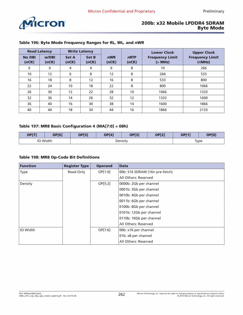
Table 196: Byte Mode Frequency Ranges for RL, WL, and nWR
Read Latency Write Latency
nWR(nCK)
nRTP(nCK)
Lower ClockFrequency Limit
(> MHz)
Upper ClockFrequency Limit
(≤≤MHz)No DBI(nCK)
w/DBI(nCK)
Set A(nCK)
Set B(nCK)
6 6 4 4 6 8 10 266
10 12 6 8 12 8 266 533
16 18 8 12 16 8 533 800
22 24 10 18 22 8 800 1066
26 30 12 22 28 10 1066 1333
32 36 14 26 32 12 1333 1600
36 40 16 30 38 14 1600 1866
40 44 18 34 44 16 1866 2133
Table 197: MR8 Basic Configuration 4 (MA[7:0] = 08h)
OP[7] OP[6] OP[5] OP[4] OP[3] OP[2] OP[1] OP[0]
IO Width Density Type
Table 198: MR8 Op-Code Bit Definitions
Function Register Type Operand Data
Type Read-Only OP[1:0] 00b: S16 SDRAM (16n pre-fetch)
All Others: Reserved
Density OP[5:2] 0000b: 2Gb per channel
0001b: 3Gb per channel
0010b: 4Gb per channel
0011b: 6Gb per channel
0100b: 8Gb per channel
0101b: 12Gb per channel
0110b: 16Gb per channel
All Others: Reserved
IO Width OP[7:6] 00b: x16 per channel
01b: x8 per channel
All Others: Reserved
Micron Confidential and Proprietary Preliminary
200b: x32 Mobile LPDDR4 SDRAMByte Mode
PDF: 09005aef8653a92d200b_z01m_sdp_ddp_qdp_mobile_lpddr4.pdf – Rev. B 4/16 EN 262 Micron Technology, Inc. reserves the right to change products or specifications without notice.
© 2015 Micron Technology, Inc. All rights reserved.
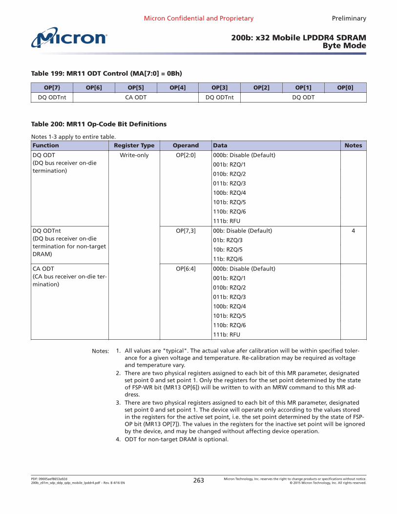
Table 199: MR11 ODT Control (MA[7:0] = 0Bh)
OP[7} OP[6] OP[5] OP[4] OP[3] OP[2] OP[1] OP[0]
DQ ODTnt CA ODT DQ ODTnt DQ ODT
Table 200: MR11 Op-Code Bit Definitions
Notes 1-3 apply to entire table.Function Register Type Operand Data Notes
DQ ODT(DQ bus receiver on-dietermination)
Write-only OP[2:0] 000b: Disable (Default)
001b: RZQ/1
010b: RZQ/2
011b: RZQ/3
100b: RZQ/4
101b: RZQ/5
110b: RZQ/6
111b: RFU
DQ ODTnt(DQ bus receiver on-dietermination for non-targetDRAM)
OP[7,3] 00b: Disable (Default) 4
01b: RZQ/3
10b: RZQ/5
11b: RZQ/6
CA ODT(CA bus receiver on-die ter-mination)
OP[6:4] 000b: Disable (Default)
001b: RZQ/1
010b: RZQ/2
011b: RZQ/3
100b: RZQ/4
101b: RZQ/5
110b: RZQ/6
111b: RFU
Notes: 1. All values are "typical". The actual value afer calibration will be within specified toler-ance for a given voltage and temperature. Re-calibration may be required as voltageand temperature vary.
2. There are two physical registers assigned to each bit of this MR parameter, designatedset point 0 and set point 1. Only the registers for the set point determined by the stateof FSP-WR bit (MR13 OP[6]) will be written to with an MRW command to this MR ad-dress.
3. There are two physical registers assigned to each bit of this MR parameter, designatedset point 0 and set point 1. The device will operate only according to the values storedin the registers for the active set point, i.e. the set point determined by the state of FSP-OP bit (MR13 OP[7]). The values in the registers for the inactive set point will be ignoredby the device, and may be changed without affecting device operation.
4. ODT for non-target DRAM is optional.
Micron Confidential and Proprietary Preliminary
200b: x32 Mobile LPDDR4 SDRAMByte Mode
PDF: 09005aef8653a92d200b_z01m_sdp_ddp_qdp_mobile_lpddr4.pdf – Rev. B 4/16 EN 263 Micron Technology, Inc. reserves the right to change products or specifications without notice.
© 2015 Micron Technology, Inc. All rights reserved.
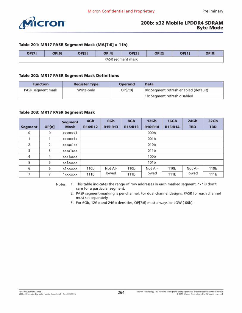
Table 201: MR17 PASR Segment Mask (MA[7:0] = 11h)
OP[7] OP[6] OP[5] OP[4] OP[3] OP[2] OP[1] OP[0]
PASR segment mask
Table 202: MR17 PASR Segment Mask Definitions
Function Register Type Operand Data
PASR segment mask Write-only OP[7:0] 0b: Segment refresh enabled (default)
1b: Segment refresh disabled
Table 203: MR17 PASR Segment Mask
Segment OP[n]Segment
Mask
4Gb 6Gb 8Gb 12Gb 16Gb 24Gb 32Gb
R14:R12 R15:R13 R15:R13 R16:R14 R16:R14 TBD TBD
0 0 xxxxxxx1 000b
1 1 xxxxxx1x 001b
2 2 xxxxx1xx 010b
3 3 xxxx1xxx 011b
4 4 xxx1xxxx 100b
5 5 xx1xxxxx 101b
6 6 x1xxxxxx 110b Not Al-lowed
110b Not Al-lowed
110b Not Al-lowed
110b
7 7 1xxxxxxx 111b 111b 111b 111b
Notes: 1. This table indicates the range of row addresses in each masked segment. "x" is don'tcare for a particular segment.
2. PASR segment-masking is per-channel. For dual channel designs, PASR for each channelmust set separately.
3. For 6Gb, 12Gb and 24Gb densities, OP[7:6} must always be LOW (-00b).
Micron Confidential and Proprietary Preliminary
200b: x32 Mobile LPDDR4 SDRAMByte Mode
PDF: 09005aef8653a92d200b_z01m_sdp_ddp_qdp_mobile_lpddr4.pdf – Rev. B 4/16 EN 264 Micron Technology, Inc. reserves the right to change products or specifications without notice.
© 2015 Micron Technology, Inc. All rights reserved.
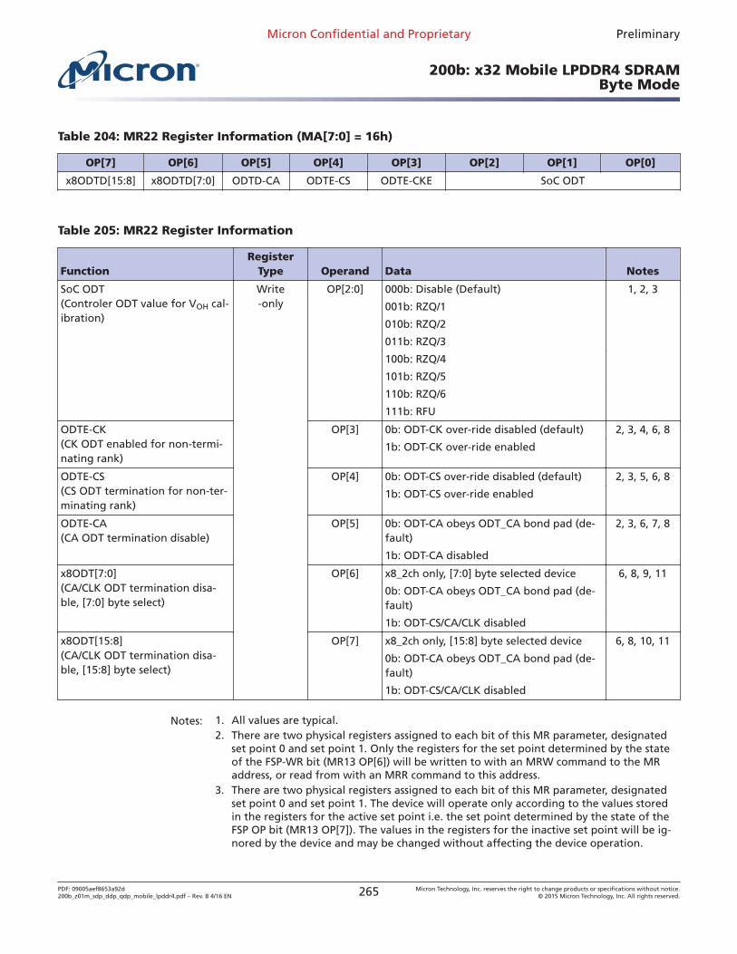
Table 204: MR22 Register Information (MA[7:0] = 16h)
OP[7] OP[6] OP[5] OP[4] OP[3] OP[2] OP[1] OP[0]
x8ODTD[15:8] x8ODTD[7:0] ODTD-CA ODTE-CS ODTE-CKE SoC ODT
Table 205: MR22 Register Information
FunctionRegister
Type Operand Data Notes
SoC ODT(Controler ODT value for VOH cal-ibration)
Write-only
OP[2:0] 000b: Disable (Default) 1, 2, 3
001b: RZQ/1
010b: RZQ/2
011b: RZQ/3
100b: RZQ/4
101b: RZQ/5
110b: RZQ/6
111b: RFU
ODTE-CK(CK ODT enabled for non-termi-nating rank)
OP[3] 0b: ODT-CK over-ride disabled (default) 2, 3, 4, 6, 8
1b: ODT-CK over-ride enabled
ODTE-CS(CS ODT termination for non-ter-minating rank)
OP[4] 0b: ODT-CS over-ride disabled (default) 2, 3, 5, 6, 8
1b: ODT-CS over-ride enabled
ODTE-CA(CA ODT termination disable)
OP[5] 0b: ODT-CA obeys ODT_CA bond pad (de-fault)
2, 3, 6, 7, 8
1b: ODT-CA disabled
x8ODT[7:0](CA/CLK ODT termination disa-ble, [7:0] byte select)
OP[6] x8_2ch only, [7:0] byte selected device 6, 8, 9, 11
0b: ODT-CA obeys ODT_CA bond pad (de-fault)
1b: ODT-CS/CA/CLK disabled
x8ODT[15:8](CA/CLK ODT termination disa-ble, [15:8] byte select)
OP[7] x8_2ch only, [15:8] byte selected device 6, 8, 10, 11
0b: ODT-CA obeys ODT_CA bond pad (de-fault)
1b: ODT-CS/CA/CLK disabled
Notes: 1. All values are typical.2. There are two physical registers assigned to each bit of this MR parameter, designated
set point 0 and set point 1. Only the registers for the set point determined by the stateof the FSP-WR bit (MR13 OP[6]) will be written to with an MRW command to the MRaddress, or read from with an MRR command to this address.
3. There are two physical registers assigned to each bit of this MR parameter, designatedset point 0 and set point 1. The device will operate only according to the values storedin the registers for the active set point i.e. the set point determined by the state of theFSP OP bit (MR13 OP[7]). The values in the registers for the inactive set point will be ig-nored by the device and may be changed without affecting the device operation.
Micron Confidential and Proprietary Preliminary
200b: x32 Mobile LPDDR4 SDRAMByte Mode
PDF: 09005aef8653a92d200b_z01m_sdp_ddp_qdp_mobile_lpddr4.pdf – Rev. B 4/16 EN 265 Micron Technology, Inc. reserves the right to change products or specifications without notice.
© 2015 Micron Technology, Inc. All rights reserved.
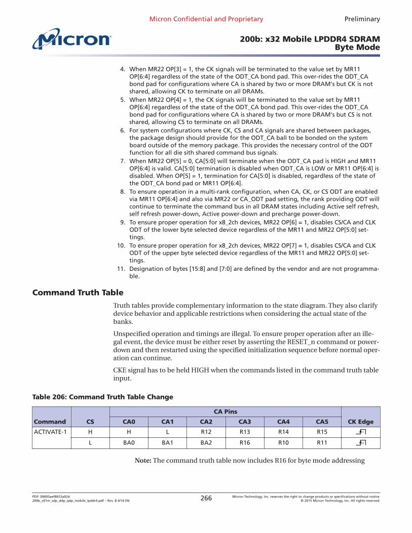
4. When MR22 OP[3] = 1, the CK signals will be terminated to the value set by MR11OP[6:4] regardless of the state of the ODT_CA bond pad. This over-rides the ODT_CAbond pad for configurations where CA is shared by two or more DRAM's but CK is notshared, allowing CK to terminate on all DRAMs.
5. When MR22 OP[4] = 1, the CK signals will be terminated to the value set by MR11OP[6:4] regardless of the state of the ODT_CA bond pad. This over-rides the ODT_CAbond pad for configurations where CA is shared by two or more DRAM's but CS is notshared, allowing CS to terminate on all DRAMs.
6. For system configurations where CK, CS and CA signals are shared between packages,the package design should provide for the ODT_CA ball to be bonded on the systemboard outside of the memory package. This provides the necessary control of the ODTfunction for all die sith shared command bus signals.
7. When MR22 OP[5] = 0, CA[5:0] will terminate when the ODT_CA pad is HIGH and MR11OP[6:4] is valid. CA[5:0] termination is disabled when ODT_CA is LOW or MR11 OP[6:4] isdisabled. When OP[5] = 1, termination for CA[5:0] is disabled, regardless of the state ofthe ODT_CA bond pad or MR11 OP[6:4].
8. To ensure operation in a multi-rank configuration, when CA, CK, or CS ODT are enabledvia MR11 OP[6:4] and also via MR22 or CA_ODT pad setting, the rank providing ODT willcontinue to terminate the command bus in all DRAM states including Active self refresh,self refresh power-down, Active power-down and precharge power-down.
9. To ensure proper operation for x8_2ch devices, MR22 OP[6] = 1, disables CS/CA and CLKODT of the lower byte selected device regardless of the MR11 and MR22 OP[5:0] set-tings.
10. To ensure proper operation for x8_2ch devices, MR22 OP[7] = 1, disables CS/CA and CLKODT of the upper byte selected device regardless of the MR11 and MR22 OP[5:0] set-tings.
11. Designation of bytes [15:8] and [7:0] are defined by the vendor and are not programma-ble.
Command Truth Table
Truth tables provide complementary information to the state diagram. They also clarifydevice behavior and applicable restrictions when considering the actual state of thebanks.
Unspecified operation and timings are illegal. To ensure proper operation after an ille-gal event, the device must be either reset by asserting the RESET_n command or power-down and then restarted using the specified initialization sequence before normal oper-ation can continue.
CKE signal has to be held HIGH when the commands listed in the command truth tableinput.
Table 206: Command Truth Table Change
Command CS
CA Pins
CK EdgeCA0 CA1 CA2 CA3 CA4 CA5
ACTIVATE-1 H H L R12 R13 R14 R15 1
L BA0 BA1 BA2 R16 R10 R11 2
Note: The command truth table now includes R16 for byte mode addressing
Micron Confidential and Proprietary Preliminary
200b: x32 Mobile LPDDR4 SDRAMByte Mode
PDF: 09005aef8653a92d200b_z01m_sdp_ddp_qdp_mobile_lpddr4.pdf – Rev. B 4/16 EN 266 Micron Technology, Inc. reserves the right to change products or specifications without notice.
© 2015 Micron Technology, Inc. All rights reserved.
Command Bus Training
The LPDDR4-SDRAM command bus must be trained before enabling termination forhigh-frequency operation. the device provides an internal VREFCA that defaults to a levelsuitable for un-terminated, low-frequency operation. The VREFCA must be trained toachieve suitable receiver voltage margin for terminated, high-frequency operation. Thetraining methodology described here centers the internal VREFCA in the CA data eye andat the same time allows for timing adjustments of the CS and CA signals to meet setup/hold requirements. Because it can be difficult to capture commands prior to trainingthe CA inputs, the training methodology described here uses a minimum of externalcommands to enter, train and exit the command bus training methodology.
Note: It is up to the system designer to determine what constitutes low-frequency andhigh-frequency based on the capabilities of the system. Low-frequency should then bedefined as an operating frequency in which the system can reliably communicate withthe device before command bus training is executed.
The byte mode device supports two command bus training (CBT) modes.
1. Mode 1: The corresponding DQ pins in this definition depends on the packageconfiguration. DQ0 becomes DQ8 in some cases, as well as DQ1 to DQ6. DQ[6:0]only used as output and the VREFCA input procedure is removed from the CBTfunction for x16 2channel. device.
2. Mode 2: TBD
Selection of which CBT mode set by MRx OP[y] (TBD).
The LPDDR4-SDRAM die has a bond pad (ODT_CA) for MULTI-RANK operation. In themulti-rank system, the terminating rank should be trained first, followed by the non-terminating rank(s). See the ODT section for more information.
Training Mode 1
The LPDDR4-SDRAM uses frequency set points (FSP) to enable multiple operating set-tings for the die. The device defaults to FSP-OP[0] at power-up, loading the default set-tings to operate in un-terminated, low-frequency environments. Prior to training, themode register settings should be configured by setting MR13 OP[6] = 1b (FSP-WR[1])and setting all other mode register bits including MR12 OP[6:0] (VREFCA range and set-ting) for FSP-OP[1] to the desired settings for high-frequency operations. Prior to enter-ing command bus training, the device will be operating from FSP-OP[x]. Upon com-mand bus training entry when CKE is driven LOW, the device will automatically switchto the alternate FSP register set (FSP OP[y]) and use the alternate register settings dur-ing training . Upon training exit when CKE is driven HIGH, the device will automaticallyswitch back to the original FSP register set (FSP-OP[x]), returning to the "known-good"state thaw was operating prior to training.
To set MRx OP[y] = 0b: CBT training mode 1
1. To enter CBT mode, issue an MRW-1 command followed by an MRW-2 commandto set MR13 OP[0] = 1b (Command bus training enabled).
2. After time tMRD, CKE may be set LOW, causing the device to switch from FSP-OP[x] to FSP-OP[y], completing entry into CBT mode. The status of DQS_t, DQS_c,DQ, and DMI are as follows
3. . After time tMRD, CKE may be set LOW, causing the device to switch from FSP-OP[x] to FSP-OP[y], and completing the entry into command bus training mode. A
Micron Confidential and Proprietary Preliminary
200b: x32 Mobile LPDDR4 SDRAMByte Mode
PDF: 09005aef8653a92d200b_z01m_sdp_ddp_qdp_mobile_lpddr4.pdf – Rev. B 4/16 EN 267 Micron Technology, Inc. reserves the right to change products or specifications without notice.
© 2015 Micron Technology, Inc. All rights reserved.
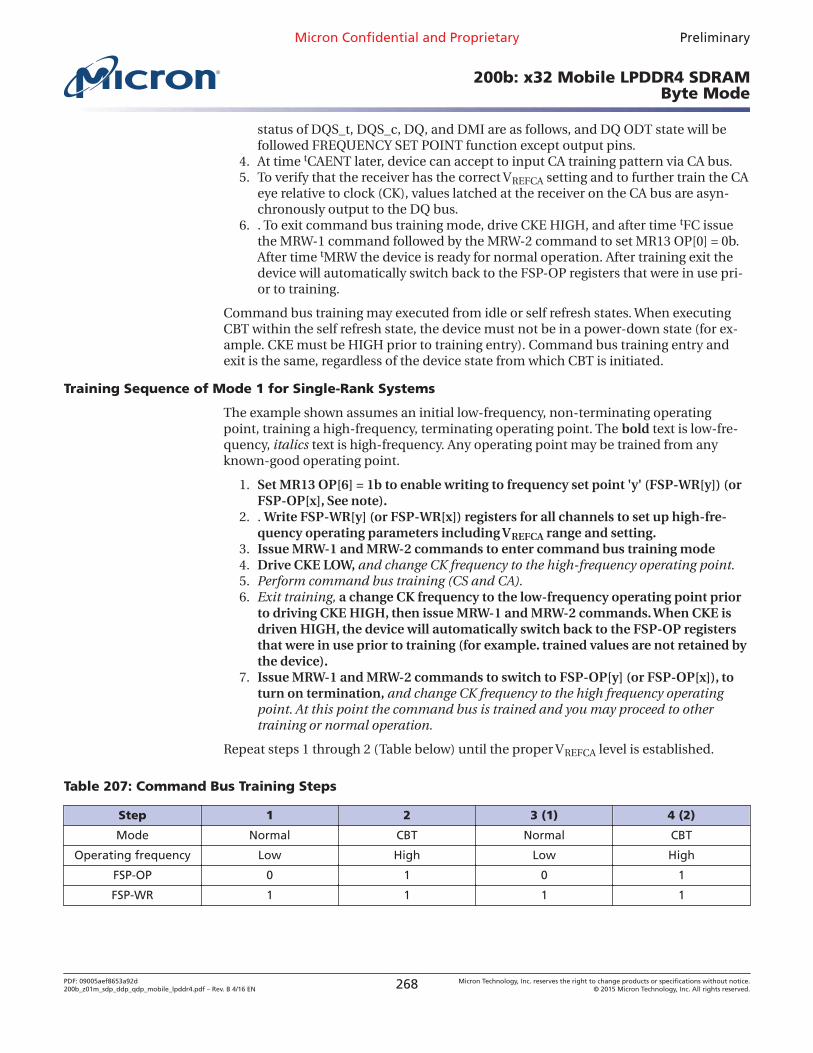
status of DQS_t, DQS_c, DQ, and DMI are as follows, and DQ ODT state will befollowed FREQUENCY SET POINT function except output pins.
4. At time tCAENT later, device can accept to input CA training pattern via CA bus.5. To verify that the receiver has the correct VREFCA setting and to further train the CA
eye relative to clock (CK), values latched at the receiver on the CA bus are asyn-chronously output to the DQ bus.
6. . To exit command bus training mode, drive CKE HIGH, and after time tFC issuethe MRW-1 command followed by the MRW-2 command to set MR13 OP[0] = 0b.After time tMRW the device is ready for normal operation. After training exit thedevice will automatically switch back to the FSP-OP registers that were in use pri-or to training.
Command bus training may executed from idle or self refresh states. When executingCBT within the self refresh state, the device must not be in a power-down state (for ex-ample. CKE must be HIGH prior to training entry). Command bus training entry andexit is the same, regardless of the device state from which CBT is initiated.
Training Sequence of Mode 1 for Single-Rank Systems
The example shown assumes an initial low-frequency, non-terminating operatingpoint, training a high-frequency, terminating operating point. The bold text is low-fre-quency, italics text is high-frequency. Any operating point may be trained from anyknown-good operating point.
1. Set MR13 OP[6] = 1b to enable writing to frequency set point 'y' (FSP-WR[y]) (orFSP-OP[x], See note).
2. . Write FSP-WR[y] (or FSP-WR[x]) registers for all channels to set up high-fre-quency operating parameters including VREFCA range and setting.
3. Issue MRW-1 and MRW-2 commands to enter command bus training mode4. Drive CKE LOW, and change CK frequency to the high-frequency operating point.5. Perform command bus training (CS and CA).6. Exit training, a change CK frequency to the low-frequency operating point prior
to driving CKE HIGH, then issue MRW-1 and MRW-2 commands. When CKE isdriven HIGH, the device will automatically switch back to the FSP-OP registersthat were in use prior to training (for example. trained values are not retained bythe device).
7. Issue MRW-1 and MRW-2 commands to switch to FSP-OP[y] (or FSP-OP[x]), toturn on termination, and change CK frequency to the high frequency operatingpoint. At this point the command bus is trained and you may proceed to othertraining or normal operation.
Repeat steps 1 through 2 (Table below) until the proper VREFCA level is established.
Table 207: Command Bus Training Steps
Step 1 2 3 (1) 4 (2)
Mode Normal CBT Normal CBT
Operating frequency Low High Low High
FSP-OP 0 1 0 1
FSP-WR 1 1 1 1
Micron Confidential and Proprietary Preliminary
200b: x32 Mobile LPDDR4 SDRAMByte Mode
PDF: 09005aef8653a92d200b_z01m_sdp_ddp_qdp_mobile_lpddr4.pdf – Rev. B 4/16 EN 268 Micron Technology, Inc. reserves the right to change products or specifications without notice.
© 2015 Micron Technology, Inc. All rights reserved.
Table 207: Command Bus Training Steps (Continued)
Step 1 2 3 (1) 4 (2)
Operation VREFCA range/value set-ting via MRW
Training pattern inputthen comparison be-
tween output data andexpected data
VREFCA range/value set-ting via MRW
Training pattern inputthen comparison be-
tween output data andexpected data.
Training Sequence of Mode 1 for Multi-Rank Systems
The a example shown here is assuming an initial low-frequency operating point, train-ing a high-frequency operating point. The bold text is low-frequency, italic text is high-frequency. Any operating point may be trained from any known-good operating point.
1. Set MR13 OP[6] = 1b to enable writing to frequency set point 'y' (FSP-WR[y]) (orFSP-WR[x].
2. Write FSP-WR[y] (or FSP-WR[x]) registers for all channels and ranks to set uphigh frequency operating parameters including VREFCA range and setting.
3. Read MR0 OP[7] on all channels and ranks to determine which die are terminat-ing, signified by MR0 OP[7] = 1b.
4. Issue MRW-1 and MRW-2 commands to enter command bus training mode onthe terminating rank.
5. Drive CKE LOW on the terminating rank (or all ranks), and change CK frequencyto the highfrequency operating point.
6. Perform command bus training on the terminating rank (CS and CA).7. Exit training by driving CKE HIGH, change CK frequency to the low-frequency oper-
ating point, and issue MRW-1 and MRW-2 commands to write the trained values toFSP-WR[y] (or FSP-WR[x]). When CKE is driven HIGH, the device will automatical-ly switch back to the FSP-OP registers that were in use prior to training.
8. Issue MRW-1 and MRW-2 command to enter training mode on the non-termi-nating rank (but keep CKE HIGH)
9. Issue MRW-1 and MRW-2 commands to switch the terminating rank to FSP-OP[y] (or FSP-OP[x]), to turn on termination, and change CK frequency to thehigh frequency operating point.
10. Drive CKE LOW on the non-terminating (or all) ranks. The non-terminatingrank(s) will now be using FSP-OP[y] (or FSP-OP[x]).
11. Perform command bus training on the non-terminating rank (CS and CA).12. Issue MRW-1 and MRW-2 commands to switch the terminating rank to FSP-OP[x]
(or FSP-OP[y]) to turn off termination.13. Exit training by driving CKE HIGH on the non-terminating rank, change CK fre-
quency to the low frequency operating point, and issue MRW-1 and MRW-2 com-mands. When CKE is driven HIGH, the device will automatically switch back tothe FSP-OP registers that were in use prior to training.
14. Write the trained values to FSP-WR[y] (or FSP-WR[x]) by issuing MRW-1 andMRW-2 commands to the device and setting all applicable mode register param-eters.
15. Issue MRW-1 and MRW-2 commands to switch the terminating rank to FSP-OP[y] (or FSP-OP[x]), to turn on termination, and change CK frequency to thehigh frequency operating point. At this point the command bus is trained for bothranks and you may proceed to other training or normal operation.
Micron Confidential and Proprietary Preliminary
200b: x32 Mobile LPDDR4 SDRAMByte Mode
PDF: 09005aef8653a92d200b_z01m_sdp_ddp_qdp_mobile_lpddr4.pdf – Rev. B 4/16 EN 269 Micron Technology, Inc. reserves the right to change products or specifications without notice.
© 2015 Micron Technology, Inc. All rights reserved.
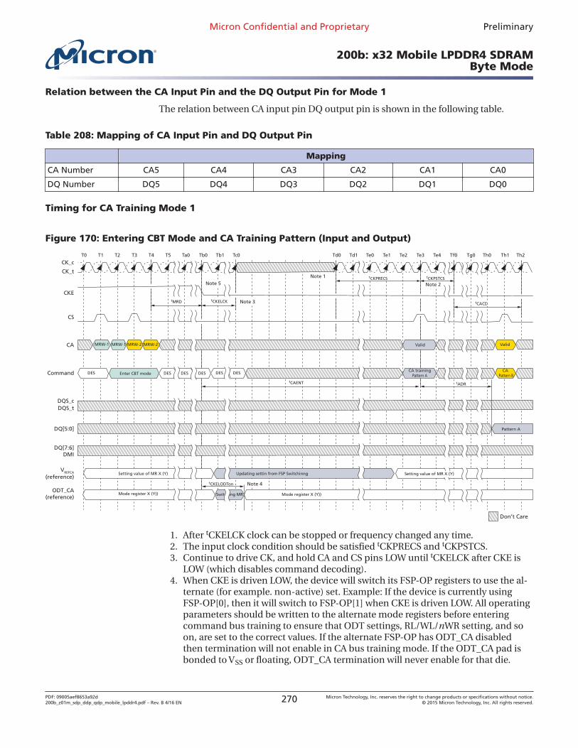
Relation between the CA Input Pin and the DQ Output Pin for Mode 1
The relation between CA input pin DQ output pin is shown in the following table.
Table 208: Mapping of CA Input Pin and DQ Output Pin
Mapping
CA Number CA5 CA4 CA3 CA2 CA1 CA0
DQ Number DQ5 DQ4 DQ3 DQ2 DQ1 DQ0
Timing for CA Training Mode 1
Figure 170: Entering CBT Mode and CA Training Pattern (Input and Output)
T0 T1 T2 T3 Tb1T4 T5 Ta0 Tb0 Tc0 Td1Td0 Te0 Te1 Te2 Te3 Tf0 Th0 Th2Te4 Tg0
CA
CK_c
CK_t
Command
MRW-1
DQS_cDQS_t
Don’t Care
MRW-1 MRW-2
DESEnter CBT mode
tMRD
CKE
CS
DES DES DES DES
DQ[5:0]
DQ[7:6]DMI
(reference)
ODT_CA(reference)
Setting value of MR X (Y)
Mode register X (Y))
MRW-2
Switching MR
Updating settin from FSP Switchinng
Mode register X (Y))
Th1
Valid
CA Pattern B
Pattern A
Valid
CA training Pattern A
tADR
DES
VREFCA
tCKPRECS tCKPSTCS
Note 2
Note 1
Note 3
Note 5
tCKELCK
tCAENT
Note 4tCKELODTon
tCACD
Setting value of MR X (Y)
1. After tCKELCK clock can be stopped or frequency changed any time.2. The input clock condition should be satisfied tCKPRECS and tCKPSTCS.3. Continue to drive CK, and hold CA and CS pins LOW until tCKELCK after CKE is
LOW (which disables command decoding).4. When CKE is driven LOW, the device will switch its FSP-OP registers to use the al-
ternate (for example. non-active) set. Example: If the device is currently usingFSP-OP[0], then it will switch to FSP-OP[1] when CKE is driven LOW. All operatingparameters should be written to the alternate mode registers before enteringcommand bus training to ensure that ODT settings, RL/WL/nWR setting, and soon, are set to the correct values. If the alternate FSP-OP has ODT_CA disabledthen termination will not enable in CA bus training mode. If the ODT_CA pad isbonded to VSS or floating, ODT_CA termination will never enable for that die.
Micron Confidential and Proprietary Preliminary
200b: x32 Mobile LPDDR4 SDRAMByte Mode
PDF: 09005aef8653a92d200b_z01m_sdp_ddp_qdp_mobile_lpddr4.pdf – Rev. B 4/16 EN 270 Micron Technology, Inc. reserves the right to change products or specifications without notice.
© 2015 Micron Technology, Inc. All rights reserved.
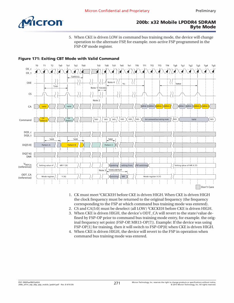
5. When CKE is driven LOW in command bus training mode, the device will changeoperation to the alternate FSP, for example. non-active FSP programmed in theFSP-OP mode register.
Figure 171: Exiting CBT Mode with Valid Command
T0 T1 T2 Ta0 Tc0Ta1 Ta2 Tb0 Td0 Tf3Tf2 Tf4 Tg0 Tg1 Tg2 Tg4Tg3 Tg5
CA
CK_c
CK_t
DQS_cDQS_t
Don’t Care
DES
CKE
CS
DES
DQ[5:0]
DQ[7:6]DMI
VREFCA(reference)
ODT_CA(reference) Mode register Y (X)
Valid
Mode register X (Y)
Setting value of MR X (Y)
MRW-1
Exit command bus training mode
tMRW
Note 1
DES
Td1 Te0 Te1 Tf0 Tf1
tCAD
CAPattern C
Pattern B Pattern C
Valid
CAPattern B
Pattern A
tADR tADR
Setting value of MR Y (X)
tCKPSTCS
Note 2
tCKCKEH
tMRZ
DES
tCKELODToff
Switching MR
DES
MRW-1 MRW-2 MRW-2 MRW-1 MRW-1 MRW-2 MRW-2
Valid DES
Updating setting from FSP switching
tFC
Note 3
DES
Note 4
DESCommand
1. CK must meet tCKCKEH before CKE is driven HIGH. When CKE is driven HIGHthe clock frequency must be returned to the original frequency (the frequencycorresponding to the FSP at which command bus training mode was entered).
2. CS and CA[5:0] must be deselect (all LOW) tCKCKEH before CKE is driven HIGH.3. When CKE is driven HIGH, the device's ODT_CA will revert to the state/value de-
fined by FSP-OP prior to command bus training mode entry, for example. the orig-inal frequency set point (FSP-OP, MR13-OP[7]). Example: If the device was usingFSP-OP[1] for training, then it will switch to FSP-OP[0] when CKE is driven HIGH.
4. When CKE is driven HIGH, the device will revert to the FSP in operation whencommand bus training mode was entered.
Micron Confidential and Proprietary Preliminary
200b: x32 Mobile LPDDR4 SDRAMByte Mode
PDF: 09005aef8653a92d200b_z01m_sdp_ddp_qdp_mobile_lpddr4.pdf – Rev. B 4/16 EN 271 Micron Technology, Inc. reserves the right to change products or specifications without notice.
© 2015 Micron Technology, Inc. All rights reserved.
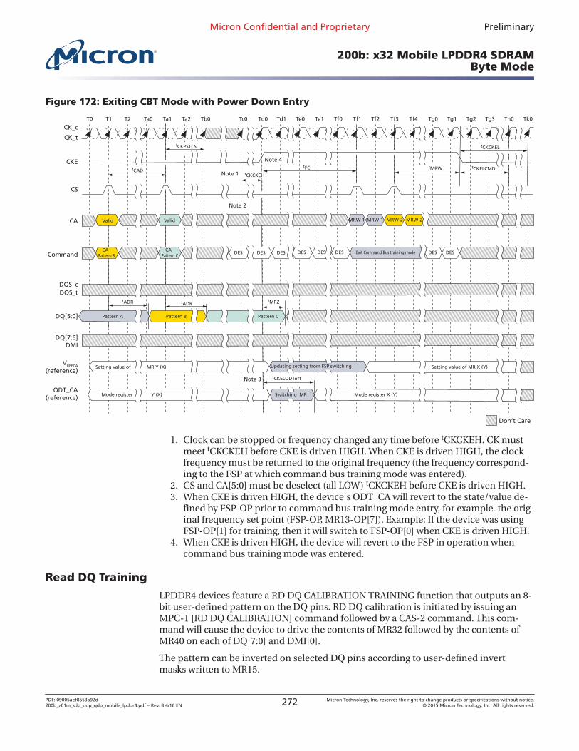
Figure 172: Exiting CBT Mode with Power Down Entry
T0 T1 T2 Ta0 Tc0Ta1 Ta2 Tb0 Td0 Tf3Tf2 Tf4 Tg0 Tg1 Tg2 Th0Tg3 Tk0
CA
CK_c
CK_t
DQS_cDQS_t
Don’t Care
DES
CKE
CS
DESDES
DQ[5:0]
DQ[7:6]DMI
(reference)
ODT_CA(reference) Mode register Y (X)
Valid
Mode register X (Y)
Setting value of MR X (Y)
MRW-1
Exit Command Bus training mode
Note 1
DES
Td1 Te0 Te1 Tf0 Tf1
tCAD
CAPattern C
Pattern B Pattern C
Valid
CAPattern B
Pattern A
tADR tADR
Setting value of MR Y (X)
tCKPSTCS
Note 2
tCKCKEH
tMRZ
DES
tCKELODToff
DES
MRW-1 MRW-2 MRW-2
DES
tFC
Note 3
Note 4
DES
tCKCKEL
tCKELCMD
VREFCA
tMRW
Command
Switching MR
Updating setting from FSP switching
1. Clock can be stopped or frequency changed any time before tCKCKEH. CK mustmeet tCKCKEH before CKE is driven HIGH. When CKE is driven HIGH, the clockfrequency must be returned to the original frequency (the frequency correspond-ing to the FSP at which command bus training mode was entered).
2. CS and CA[5:0] must be deselect (all LOW) tCKCKEH before CKE is driven HIGH.3. When CKE is driven HIGH, the device's ODT_CA will revert to the state/value de-
fined by FSP-OP prior to command bus training mode entry, for example. the orig-inal frequency set point (FSP-OP, MR13-OP[7]). Example: If the device was usingFSP-OP[1] for training, then it will switch to FSP-OP[0] when CKE is driven HIGH.
4. When CKE is driven HIGH, the device will revert to the FSP in operation whencommand bus training mode was entered.
Read DQ Training
LPDDR4 devices feature a RD DQ CALIBRATION TRAINING function that outputs an 8-bit user-defined pattern on the DQ pins. RD DQ calibration is initiated by issuing anMPC-1 [RD DQ CALIBRATION] command followed by a CAS-2 command. This com-mand will cause the device to drive the contents of MR32 followed by the contents ofMR40 on each of DQ[7:0] and DMI[0].
The pattern can be inverted on selected DQ pins according to user-defined invertmasks written to MR15.
Micron Confidential and Proprietary Preliminary
200b: x32 Mobile LPDDR4 SDRAMByte Mode
PDF: 09005aef8653a92d200b_z01m_sdp_ddp_qdp_mobile_lpddr4.pdf – Rev. B 4/16 EN 272 Micron Technology, Inc. reserves the right to change products or specifications without notice.
© 2015 Micron Technology, Inc. All rights reserved.
RD DQ Calibration Training Procedure
The procedure for executing RD DQ calibrations is:
Issue MRW commands to write MR32 (first 8 bits), MR40 (second 8 bits), MR15 (eight-bit invert mask for byte 0: DQ[7:0] and MR20 (eight-bit invert mask for byte 1: DQ[15:8].Optionally this step could be skipped to use default patterns:
• MR32 default = 5Ah• MR40 default = 3Ch• MR15 default = 55h• MR20 default = 55h
Issue an MPC-1 [RD DQ CALIBRATION] command followed immediately be a CAS-2command
• Each time an MPC-1 [RD DQ CALIBRATION] command followed by a CAS-2 is re-ceived by the device, a 16-bit data burst will, after the currently set RL, drive the eightbits programmed in MR32 followed by the eight bits programmed in MR40 on all I/Opins.
• The data pattern will be inverted for I/O pins with a 1 programmed in the corre-sponding invert mask mode register bit ( see the Invert Mask Assignments Table).
Note: The pattern is driven on the MCI pins, but no data bus inversion func-tion is enabled, even if read DBI is enabled in the device mode register.
• The MPC-1 command can be issued every tCCD seamlessly, and tRTRRD delay is re-quired between ARRAY READ command and the MPC-1 command as well the delayrequired between the MPC-1 command and an ARRAY READ.
• The operands received with the CAS-2 command must be driven LOW• DQ read training can be performed with any or no banks active, during REFRESH, or
during SREF with CKE HIGH.
Table 209: Invert Mask Assignments
Invert Mask Assignments
DQ pin 0 1 2 3 DMI0 4 5 6 7
MR15 bit 0 1 2 3 N/A 4 5 6 7
DQ pin 8 9 10 11 DMI1 12 13 14 15
MR20 bit 0 1 2 3 N/A 4 5 6 7
Notes: 1. The patterns contained in MR32 and MR40 are transmitted on the lower byte: DQ[7:0]or the upper byte: DQ[15:8] when a RD DQ calibration is initiated via an MPD-1 [RD DQCALIBRATION] command. The pattern is transmitted serially on each data land, organ-ized as little endian such that the low-order bit in the byte is transmitted first. If the da-ta pattern is 27h, the fist bit transmitted will be a 1 followed by 1, 1, 0, 0, 1, 0, and 0.The bit stream will be 00100111...
2. MR15 and MR22 may be used to invert the MR32/MR40 data patterns on the DQ pins.Refer to the MR15 description for more information. Data is never inverted on theDMI[1:0] pins.
3. The data pattern is not transmitted on the DMI[1;0] pins if DBI-RD is disabled via MR3OP[6].
4. No DATA BUS INVERSION (DBI) function is enacted during RD DQ calibrations, even ifDBI is enabled in MR3 OP[6].
Micron Confidential and Proprietary Preliminary
200b: x32 Mobile LPDDR4 SDRAMByte Mode
PDF: 09005aef8653a92d200b_z01m_sdp_ddp_qdp_mobile_lpddr4.pdf – Rev. B 4/16 EN 273 Micron Technology, Inc. reserves the right to change products or specifications without notice.
© 2015 Micron Technology, Inc. All rights reserved.
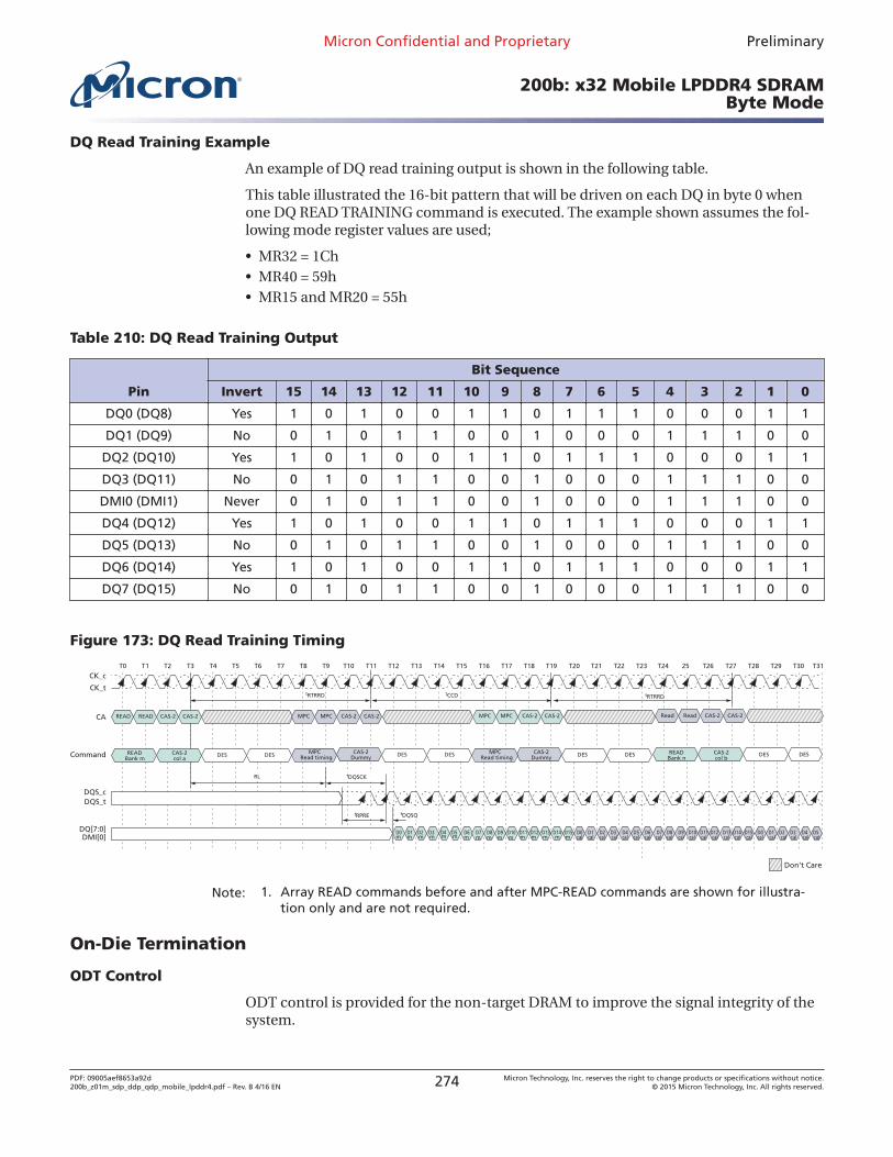
DQ Read Training Example
An example of DQ read training output is shown in the following table.
This table illustrated the 16-bit pattern that will be driven on each DQ in byte 0 whenone DQ READ TRAINING command is executed. The example shown assumes the fol-lowing mode register values are used;
• MR32 = 1Ch• MR40 = 59h• MR15 and MR20 = 55h
Table 210: DQ Read Training Output
Pin
Bit Sequence
Invert 15 14 13 12 11 10 9 8 7 6 5 4 3 2 1 0
DQ0 (DQ8) Yes 1 0 1 0 0 1 1 0 1 1 1 0 0 0 1 1
DQ1 (DQ9) No 0 1 0 1 1 0 0 1 0 0 0 1 1 1 0 0
DQ2 (DQ10) Yes 1 0 1 0 0 1 1 0 1 1 1 0 0 0 1 1
DQ3 (DQ11) No 0 1 0 1 1 0 0 1 0 0 0 1 1 1 0 0
DMI0 (DMI1) Never 0 1 0 1 1 0 0 1 0 0 0 1 1 1 0 0
DQ4 (DQ12) Yes 1 0 1 0 0 1 1 0 1 1 1 0 0 0 1 1
DQ5 (DQ13) No 0 1 0 1 1 0 0 1 0 0 0 1 1 1 0 0
DQ6 (DQ14) Yes 1 0 1 0 0 1 1 0 1 1 1 0 0 0 1 1
DQ7 (DQ15) No 0 1 0 1 1 0 0 1 0 0 0 1 1 1 0 0
Figure 173: DQ Read Training Timing
T0 T1 T2 T3 T8T4 T5 T6 T7 T9 T10 T14T11 T12 T13 T16T15 T17 T18 T19 T20 T22 T24 T2825 T26 T27 T30T29 T31T21 T23
CA
CK_c
CK_t
Command
READ READ
READBank m
DQS_cDQS_t
DQ[7:0]DMI[0]
Don’t Care
t
ValidCAS-2 MPC CAS-2MPC CAS-2CAS-2
DES DESCAS-2col a
CAS-2Dummy
MPC Read timing
MPC MPC CAS-2 Read CAS-2Read CAS-2
DES DES CAS-2Dummy
MPC Read timing DES DES READ
Bank nDES DESCAS-2
col b
t
D0m
D1m
D2m
D3m
D4m
D5m
D6m
D7m
D8m
D9m
D10m
D11m
D12m
D13m
D14m
D15m
D0cal
D1cal
D2cal
D3cal
D4cal
D5cal
D6cal
D7cal
D8cal
D9cal
D10cal
D11cal
D12cal
D13cal
D14cal
D15cal
D0cal
D1cal
D2cal
D3cal
D4cal
D5cal
tCCD tRTRRD
CAS-2
tRTRRD
tDQSQRPRE
DQSCKRL t
Note: 1. Array READ commands before and after MPC-READ commands are shown for illustra-tion only and are not required.
On-Die Termination
ODT Control
ODT control is provided for the non-target DRAM to improve the signal integrity of thesystem.
Micron Confidential and Proprietary Preliminary
200b: x32 Mobile LPDDR4 SDRAMByte Mode
PDF: 09005aef8653a92d200b_z01m_sdp_ddp_qdp_mobile_lpddr4.pdf – Rev. B 4/16 EN 274 Micron Technology, Inc. reserves the right to change products or specifications without notice.
© 2015 Micron Technology, Inc. All rights reserved.
A non-target DRAM is defines as one that receives a WRITE-1, MASK WRITE-1, READ-1,MODE REGISTER READ-1, MPC (only WRITE FIFO, READ FIFO and READ DQ CALI-BRATION) command but does not receive a corresponding CAS-2 command (WRITE-2,MASK WRITE-2, READ-2, MODE REGISTER READ-2, MPC). The controller must issuetwo DES commands in place of a CAS-2 command to the non-target DRAM.
The ODT mode for non-target DRAM is enabled if MR11 OP[7,3] is set to a non-zero val-ue. The ODT mode for non-target DRAM is disabled if MR11 OP[7,3] = 00b.
CKE must be HIGH to control ODT on the non-target rank. The DRAM may still be inthe self refresh state but CKE has to be HIGH to control ODT on the non-target rank.
WRITE-1, MASK WRITE-1, MPC (WRITE FIFO) case:
• The CAS-2 command is replaced by two DES commands for the non-target DRAM.• ODT timings (ODTon and ODTLoff) are referenced to the second of the DES com-
mands.• ODT latency values remain the same as for normal DQ ODT control as shown in ODT-
Lon and ODTLoff Latency Values table in DQ On-Die Termination section.
READ-1, MODE REGISTER READ-1, MPC (READ FIFO and READ DQ CALIBRATION)case: Refer to the table below.
• The CAS-2 command is replaced by two DES commands for the non-target DRAM.• ODT timings (ODTon and ODTLoff) are referenced to the second of the DES com-
mands.
Table 211: ODTLon_rd and ODTLoff_rd Latency Values (Non Target DRAM)
ODTLon_rd Latency ODTLoff_rd Latency 1, 2 Lower ClockFrequency Limit
(MHz)
Upper ClockFrequency Limit
(MHz)No DBI w/DBI No DBI w/DBI
Not Supported Not Supported Not Supported Not Supported 10 266
Not Supported Not Supported Not Supported Not Supported 266 533
Not Supported Not Supported Not Supported Not Supported 533 800
14 16 32 34 800 1066
18 22 36 40 1066 1333
22 26 42 46 1333 1600
26 30 46 50 1600 1866
28 32 50 54 1866 2133
Notes: 1. ODTLoff_rd assumes BL = 16, for BL32, 8tCK should be added.2. ODTLoff_rd assumes a fixed tRPST of 1.5tCK. (DRAM will assume 1.5tCK independent of
MR settings)3. ODT for non-target DRAM is optional.
Micron Confidential and Proprietary Preliminary
200b: x32 Mobile LPDDR4 SDRAMByte Mode
PDF: 09005aef8653a92d200b_z01m_sdp_ddp_qdp_mobile_lpddr4.pdf – Rev. B 4/16 EN 275 Micron Technology, Inc. reserves the right to change products or specifications without notice.
© 2015 Micron Technology, Inc. All rights reserved.
AC Timing
Table 212: Core AC Timing
Parameter SymbolMin/Max
Data Rate
Unit533 1066 1600 2133 2667 3200 3733 4267
Write recovery time tWR Min max(20ns, 4nCK) ns
Write-to-Read delay tWTR Min max(12ns, 8nCK) ns
Table 213: CBT AC Timing for Mode 1
Parameter SymbolMin/Max
Data Rate
Unit Note533 1066 1600 2133 2667 3200 3733 4267
Clock and command validafter CKE LOW
tCKEKCK Min max(7.5ns, 3nCK) tCK
Asynchronous data read tADR Max 20ns ns
CA BUS TRAINING com-mand to CA BUS TRAIN-ING command delay
tCACD Min RU(tADR/tCK) tCK 1
First CA BUS TRAININGcommand following CKELOW
tCAENT Min 250 ns
Valid clock requirementbefore CS HIGH
tCKPRECS Min 2tCK + tXP (tXP = max(7.5ns, 5nCK)) -
Valid clock requirementafter CS HIGH
tCKPSTCS Min max(7.5ns, 5nCK) -
Clock and command validbefore CKE HIGH
tCKCKEH Min 2 tCK
CA bus training CKE HIGHto DQ tri-state
tMRZ Min 1.5 ns
ODT turn-on latency fromCKE
tCKELODTon Min 20 ns
ODT turn-off latencyfrom CKE
tCKELODToff Min 20 ns
Note: 1. If tCACD is violated, the data for samples which violate tCACD will not be available ex-cept for the last sample (where tCACD after this sample is met). Valid data for the lastsample will be available after tADR.
Table 214: AC Timing Parameters for 2 channel x8 CBT Mode
Symbol Parameter Max/Min Value UnittLZDQ7H x8 CBT mode DQ[5:0] output LOW-Z time from DQ[7] HIGH Min 2 nstHZDQ7L x8 CBT mode DQ[5:0] output HIGH-Z time from DQ[7] LOW Max 10 nstDQSDQ7 x8 CBT mode VREFCA value/range strobe to DQ[7] HIGH Min 10 ns
Micron Confidential and Proprietary Preliminary
200b: x32 Mobile LPDDR4 SDRAMByte Mode
PDF: 09005aef8653a92d200b_z01m_sdp_ddp_qdp_mobile_lpddr4.pdf – Rev. B 4/16 EN 276 Micron Technology, Inc. reserves the right to change products or specifications without notice.
© 2015 Micron Technology, Inc. All rights reserved.
Table 214: AC Timing Parameters for 2 channel x8 CBT Mode (Continued)
Symbol Parameter Max/Min Value UnittDQ7DQS x8 CBT mode DQ[7] LOW to VREFCA value/range strobe Min 15 nstDQ7CS x8 CBT mode DQ[7] HIGH to CA/CA latch Min 0 ns
Micron Confidential and Proprietary Preliminary
200b: x32 Mobile LPDDR4 SDRAMByte Mode
PDF: 09005aef8653a92d200b_z01m_sdp_ddp_qdp_mobile_lpddr4.pdf – Rev. B 4/16 EN 277 Micron Technology, Inc. reserves the right to change products or specifications without notice.
© 2015 Micron Technology, Inc. All rights reserved.
Revision History
Rev. B– 4/16
• Updated IDD specifications• Deleted Low-Frequency Operation section• Added Monolithic Device Addressing (1 channel) in Monolithic Device Addressing• Updated MR8 Op-Code Bit Definitions table in Mode Registers• Updated MR17 PASR Segment Mask table in Mode Registers• Updated Refresh Requirement Parameter table in Refresh Requirement
Rev. A – 7/15
• Initial release
8000 S. Federal Way, P.O. Box 6, Boise, ID 83707-0006, Tel: 208-368-4000www.micron.com/products/support Sales inquiries: 800-932-4992
Micron and the Micron logo are trademarks of Micron Technology, Inc.All other trademarks are the property of their respective owners.
This data sheet contains initial characterization limits that are subject to change upon full characterization of production devices.
Micron Confidential and Proprietary Preliminary
200b: x32 Mobile LPDDR4 SDRAMRevision History
PDF: 09005aef8653a92d200b_z01m_sdp_ddp_qdp_mobile_lpddr4.pdf – Rev. B 4/16 EN 278 Micron Technology, Inc. reserves the right to change products or specifications without notice.
© 2015 Micron Technology, Inc. All rights reserved.