Embed Size (px)
Citation preview
MOVING TECHNOLOGY TO MARKET™
EXHIBITION GUIDE
www.spie.org/al
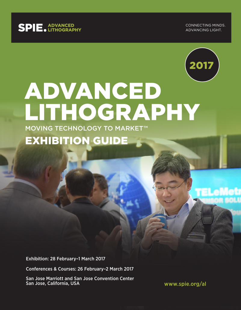
ADVANCEDLITHOGRAPHY
Exhibition: 28 February–1 March 2017
Conferences & Courses: 26 February–2 March 2017
San Jose Marriott and San Jose Convention Center San Jose, California, USA
CONNECTING MINDS. ADVANCING LIGHT.
2017

ADVANCED LITHOGRAPHY 2017THE PREMIER EVENT FOR THE SEMICONDUCTOR INDUSTRY
Exhibition: 28 February–1 March 2017
Conferences & Courses: 26 February–2 March 2017
San Jose Marriott and San Jose Convention Center San Jose, California, USA
Five Days Many Opportunities
CUTTING-EDGE RESEARCH AND COURSES
PLENARY PRESENTATIONS AND EXHIBITION
www.spie.org/al
CONNECTING MINDS. ADVANCING LIGHT.

Onsite News: www.spie.org/ALnews · #SPIElitho 1
For information about exhibiting, sponsorship, and advertising opportunities at future Advanced Lithography events, contact: SPIE Sales at [email protected]
CONTENTSSponsors . . . . . . . . . . . . . . . . . . . . . . . . . . . . . . . . . . . X
Exhibitor Index. . . . . . . . . . . . . . . . . . . . . . . . . . . . . . X
Exhibition Floor Plan. . . . . . . . . . . . . . . . . . . . . . . . . X
General Information . . . . . . . . . . . . . . . . . . . . . . . . . X
Course Daily Schedule . . . . . . . . . . . . . . . . . . . . . . . X
Exhibitor Directory . . . . . . . . . . . . . . . . . . . . . . . . . . X
Product Categories . . . . . . . . . . . . . . . . . . . . . . . . . . X
Policies . . . . . . . . . . . . . . . . . . . . . . . . . . . . . . . . . . . 1X
Corporate Members . . . . . . . . . . . . . . . . . . . . . . . . . X
Sponsored by
SPIE would like to express its deepest appreciation to the symposium chairs, conference chairs, program committees, session chairs, and authors who have so generously given their time and advice to make this symposium possible.
The symposium, like our other conferences and activities, would not be possible without the dedicated contribution of our participants and members. This program is based on commitments received up to the time of publication and is subject to change without notice.
Welcome to the ExhibitionTuesday 28 February · 10:00 AM to 5:00 PMWednesday 1 March · 10:00 AM to 4:00 PM
2 SPIE Advanced Lithography 2017 · www.spie.org/al · +1 360 676 3290 · [email protected]
Thanks to the following sponsors for their generous support of SPIE Advanced Lithography
TM
General Sponsors:JSR Micro, Inc.
Hitachi High TechnologiesMicro Lithography Inc.
Qoniac GmbHSolar-Semi
Onsite News: www.spie.org/ALnews · #SPIElitho 3
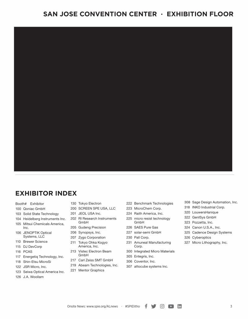
SAN JOSE CONVENTION CENTER · EXHIBITION FLOOR
201 205 207
100 104 106
323 325 327 331
222 224 226 230
301 303 305 307
200 202 206
211 213
110
217 219 221
116 118
223 225 227 231
122 126 130
103 105 111 113 115 117 121 123
Entrance
Exhibitor Service Area and Lounge
Posters ReceptionTuesday 6:00 to 8:00 pm
Lunch/Seating Area
Coffee Area
300 302 304 306 322 324 326 328
Main
Entrance
308 310 312 314 316 318 320
EXHIBITOR INDEXBooth# Exhibitor
100 QoniacGmbH
103 SolidStateTechnology
104 HeidelbergInstrumentsInc.
105 MitsuiChemicalsAmerica,Inc.
106 JENOPTIKOpticalSystems,LLC
110 BrewerScience
115 DJDevCorp
116 PCAS
117 EnergetiqTechnology,Inc.
118 Shin-EtsuMicroSi
122 JSRMicro,Inc.
123 SeiwaOpticalAmericaInc.
126 J.A.Woollam
222 BenchmarkTechnologies
223 MicroChemCorp.
224 RaithAmerica,Inc.
225 microresisttechnologyGmbH
226 SAESPureGas
227 solar-semiGmbH
230 PallCorp.
231 AmunealManufacturingCorp.
300 IntegratedMicroMaterials
305 Entegris,Inc.
306 Coventor,Inc.
307 attocubesystemsInc.
130 TokyoElectron
200 SCREENSPEUSA,LLC
201 JEOLUSAInc.
202 RIResearchInstrumentsGmbH
205 GudengPrecision
206 Synopsys,Inc.
207 ZygoCorporation
211 TokyoOhkaKogyoAmerica,Inc.
213 VistecElectronBeamGmbH
217 CarlZeissSMTGmbH
219 AbeamTechnologies,Inc.
221 MentorGraphics
308 SageDesignAutomation,Inc.
318 INKOIndustrialCorp.
320 LouwersHanique
322 GenISysGmbH
323 Pozzetta,Inc.
324 CanonU.S.A.,Inc.
325 CadenceDesignSystems
326 Cyberoptics
327 MicroLithography,Inc.

4 SPIE Advanced Lithography 2017 · www.spie.org/al · +1 360 676 3290 · [email protected]
GENERAL INFORMATION
Exhibition HoursTuesday 28 February · 10:00 am to 5:00 pmWednesday 1 March · 10:00 am to 4:00 pm
RegistrationSan Jose Convention Center
Sunday 26 February · 7:15 am to 5:00 pmMonday 27 February · 7:15 am to 4:00 pmTuesday 28 February · 7:30 am to 5:00 pmWednesday 1 March · 7:30 am to 4:00 pmThursday 2 March · 7:45 am to 4:00 pm (Thursday is conference registration only)
Coffee BreaksServed daily – 7:30 am, 10:00 am and 3:00 pm
Check individual conference listings for exact times and locations.Sponsors:
Breakfast BreadsConvention Center, Ballroom ConcourseMonday – Thursday, 7:30 am
Wednesday Sponsors:
Food and Refreshments for PurchaseConvention Center, Ballroom ConcourseMonday – Thursday, 7:30 am to 3:00 pm
Hot and cold snacks, hot entrees, deli sandwiches, salads, and pastries are available for purchase. Cash and credit cards accepted.
Exhibition Hall Concession StandTuesday – Wednesday, 11:00 am to 2:00 pm
Hot and cold snacks, hot entrees, deli sandwiches, salads, and pastries are available for purchase. Cash and credit cards accepted.
SPIE Hosted Lunches Exhibition HallTuesday – Wednesday, 11:30 am to 1:00 pm
Check individual conference listings for exact times. Complimentary tickets for these lunches will be included with full conference registrations. Exhibitors and students may purchase tickets at the Cashier Desk. Sponsors:
Desserts Exhibition Hall 1 Tuesday and Wednesday
Complimentary tickets for the dessert snacks will be included in conference attendee registration packets.
Internet OptionsWireless Access – Convention Center Upper Level ConcourseComplimentary wireless access is also available; instructions will be posted onsite.West end WiFi sponsored by
East end WiFi sponsored by
TM
SPIE Conference and Exhibition AppSearch and browse the program, special events, participants, exhibitors, courses, and more. Free Conference App available for iPhone and Android phones.
SPIE BookstoreConvention Center Lobby near Registration
Stop by the SPIE Bookstore to browse the latest SPIE Press Books, proceedings, and educational materials. While there, get a t-shirt or educational toy to bring home to the family.
Restaurant Reservations and Information Desk The San Jose Convention and Visitors Bureau operates a Restaurant Reservations and Information Desk on the street level of the Convention Center near the main entrance. The desk will be open Sunday through Thursday during core hours of the convention. For more information visit their website http://www.sanjose.org
Onsite News: www.spie.org/ALnews · #SPIElitho 5
MONEY-BACK GUARANTEEWe are confident that once you experience an SPIE course for yourself you will look to us for your future education needs. However, if for any reason you are dissatisfied, we will gladly refund your money. We just ask that you tell us what you did not like; suggestions for improvement are always welcome.
Get training.Stay competitive.Advance your career.· Direct instruction from
legends in the semi/litho industry, many of whom are pioneers in their fields
· Course topics are continually updated and aligned with current industry needs and trends
· Earn CEUs for professional continuing education requirements
· SPIE offers online courses and in-company training, www.spie.org/education
SUNDAY SC101Introduction to Microlithography: Theory, Materials, and Processing (Willson, Bowden) Sunday8:30amto5:30pm,$600/$710/$359
SC1099Chemistry and Lithography (Okoroanyanwu)Sunday8:30amto5:30pm,$700/$810/$399
SC1100Scatterometry in Profile, Overlay and Focus Process Control (Cramer, Turovets) Sunday1:30pmto5:30pm,$375/$430/$247
SC1132Computational Basis for Advanced Lithography Techniques (Lai) Sunday8:30amto12:30pm,$375/$430/$247
SC1133 Metrology Toolset Monitoring, Matching, Maintenance and Management (Solecky, Adan) Sunday8:30amto12:30pm$375/$430/$247
SC1158 Metrology of Image Placement (Starikov) Sunday1:30pmto5:30pm,$380/$435/$249
SC1172Spatial Coherence and Impact on Lithography Simulation and OPC (Kang) Sunday8:30amto12:30pm,$375/$430/$247
SC1173How and Why: The big ideas in semiconductor lithography (Mack, Petersen) Sunday8:30amto5:30pm,$685/$795/$393
NEWSC1209Data Analytics and Machine
Learning in Semiconductor Manufacturing: Applications for Physical Design, Process and Yield Optimization (Cain, Capodieci) Sunday1:30pmto5:30pm,$375/$430/$247
SC885Principles and Practical Implementation of Multiple Patterning (Dusa, Hsu) Sunday8:30amto5:30pm,$600/$710/$359
SC888EUV Lithography (Bakshi, Ahn, Naulleau) Sunday8:30amto5:30pm,$740/$850/$415
SC992 Lithography Integration for Semiconductor FEOL & BEOL Fabrication (Lin, Zhang) Sunday8:30amto5:30pm,$600/$710/$359
CONTINUING EDUCATION UNITSSPIE is accredited by the International Association for Continuing Education and Training (IACET) and is authorized to issue the IACET CEU.
WEDNESDAY SC1187Understanding Design-Patterning Interactions for EUV and DSA (Gupta, Torres, Mallik) Wednesday1:30pmto5:30pm,$375/$430/$247
THURSDAY SC616Practical Photoresist Processing (Dammel) Thursday8:30amto12:30pm,$375/$430/$247
COURSES
PRICE KEY: Member / Non Member / Student Member
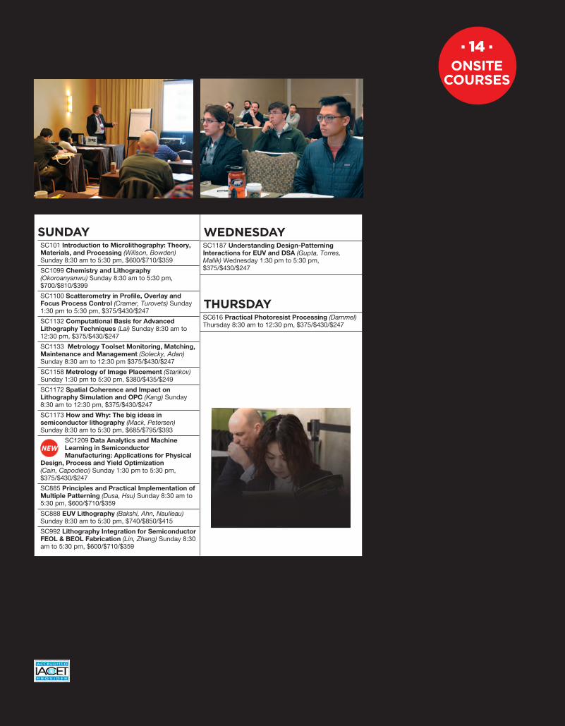
· 14 · ONSITE
COURSES
SPIE STUDENT MEMBERS RECIEVE DISCOUNTED COURSE PRICES.
SEE FULL COURSE DESCRIPTIONS AND REGISTER FOR COURSES ONSITE.
Course descriptions also available online: www.spie.org/ALCourses
6 SPIE Advanced Lithography 2017 · www.spie.org/al · +1 360 676 3290 · [email protected]
Abeam Technologies, Inc. #21922290FoothillBlvdSte2,Hayward,CA,94541UnitedStates+15104970222;[email protected];www.abeamtech.comContact:SergeyBabin,President
Amuneal Manufacturing Corp. #2314737DarrahSt,Philadelphia,PA,[email protected];www.amuneal.com
Featured Product: Magnetic Shielding Design and Fabrication
Since1965,Amunealhasbeenservinghighlytechnicalmarkets,workingwithleadersinaerospace,electronics,cryogenics,healthcare,andresearchtodevelopcost-effectivemagneticshieldingstrategiesandproductsthatoutperformthemostdemandingrequirements.Weofferanumberofstandardcomponentshieldstoourclients,however,ourcultureandcapabilitiesallowustomanufactureandinstalluniquecustomshieldsrangingfromprototypesandmodelstofull-scaleassemblies.Contact:MichaelAdolf,Director,TechnicalProducts,[email protected];StuartKoch,VP,TechnicalProducts,[email protected]
attocube systems Inc. #307
2020StuartSt,Berkeley,CA,[email protected];www.attocube.comattocubeisawell-establishedpremium-qualitymanufacturerforhighprecisionpiezopositioningdevices,opticaldisplacementsensorsandcryogenicmeasurementsystems.TheattoDRY800istheworld’sfirstcryo-opticaltableandtheperfectchoiceforlowtemperaturequantumopticsexperiments.attocube’srenownedpiezostagesenablenanometerprecisepositioningevenunderextremeenvironmentalconditionssuchascryogenictemperatures,highmagneticfieldsandhighorultra-highvacuum.
Benchmark Technologies #2227KimballLn,Lynnfield,MA,01940-2654UnitedStates+17812463303;[email protected];www.benchmarktech.comContact:AndrewZanzal,VicePresidentofSales
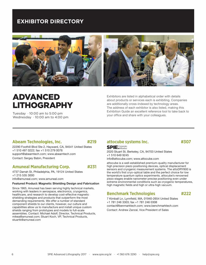
Exhibition Directory
EXHIBITOR DIRECTORY
Tuesday · 10:00 am to 5:00 pmWednesday · 10:00 am to 4:00 pm
ADVANCED LITHOGRAPHY
Exhibitorsarelistedinalphabeticalorderwithdetailsaboutproductsorserviceseachisexhibiting.Companiesareadditionallycross-indexedbytechnologyareas.Theaddressofeachexhibitorisalsolisted,makingthisExhibitionGuideanexcellentreferencetooltotakebacktoyourofficeandsharewithyourcolleagues.
Onsite News: www.spie.org/ALnews · #SPIElitho 7
EXHIBITOR DIRECTORY
SPONSOR
Brewer Science #110
2401BrewerDr,Rolla,MO,65401-7003UnitedStates+15733640300;[email protected];www.brewerscience.com
Featured Product: OptiStack® multilayer systems are designed for advanced high-volume manufacturing processes.
BrewerScienceisaglobaltechnologyleaderindevelopingandmanufacturinginnovativematerialsandprocesses,forthefabricationofsemiconductorsandmicroelectronicdevices.Today,wecontinuetoexpandourtechnologyportfoliotoincludeproductsthatenableadvancedlithography,3-Dintegration,chemicalandmechanicaldeviceprotection,nanotechnology,andthinwaferhandling.BrewerScienceispreparedforthenextgeneration.Areyou?Findoutathttp://www.brewerscience.com.Contact:AlexSmith,DirectorofSales,[email protected];BrentScott,SeniorAccountManager,[email protected]
Cadence Design Systems #3252655SeelyAve,SanJose,CA,95134-1931UnitedStates+14089431234www.cadence.com
Featured Product: Litho Physical Analyzer, Cadence CMP Predictor, Litho Electrical Analyzer, Cadence Pattern Analysis LDE
Cadenceenablesglobalelectronicdesigninnovationandplaysanessentialroleinthecreationoftoday’sintegratedcircuitsandelectronics.CustomersuseCadencesoftware,hardware,IP,andservicestodesignandverifyadvancedsemiconductors,consumerelectronics,networkingandtelecommunicationsequipment,andcomputersystems.Inparticular,Cadence®DFMsolutionsaddressbothdesignerandmanufacturerchallengesresultinginimproveddesignmanufacturabilityandreducedtimetoyield.Contact:PhilippeHurat,ProductMarketing,Director
SPONSOR
Canon U.S.A., Inc. #324
IndustrialProductsDivision,3300NFirstSt,SanJose,CA,[email protected];usa.canon.com/industrial
Featured Product: FPA-1200NZ2C
CanonUSAIndustrialProductsDivisionprovidesadvancedwafer&panelprocessequipmentforapplicationsincludingsemiconductor,AdvancedPackaging&display.Canonprovidescost-effectivewaferprocessingsolutionsincludingi-line&KrFopticallithography,nanoimprintlithography&CanonAnelvadepositionequipment.Canonalsohasavarietyofpanelbasedlithography&depositionsolutionsthatcanbeextendedtoavarietyofapplications.Contactsemi-info@cusa.canon.comformoreinfo.Contact:DougShelton,MarketingManager,[email protected]
SPONSOR
Carl Zeiss SMT GmbH #217CarlZeissPromenade10,Jena,07745Germany+493641642563;[email protected];www.zeiss.com/mask-solutions
Featured Product: ZEISS ForTune | High performance Wafer and Mask Tuning system
TheZEISSstrategicbusinessunitSemiconductorMetrologySystems(SMS)specializesinakeyprocessinsemiconductormanufacturing:thephotomask.Coreexpertiseinlightandelectronoptics,complementedbyapioneeringfemto-secondlasertechnologyformthefoundationofaproductportfoliocomprisingin-diemetrology,actinicqualification,repair,andtuningofphotomasks.Toincreaseautomationandenhancetoolcapabilities,SMSalsooffersadvancedsoftwareapplications.Contact:CarlZeissSMTGmbH,StrategicBusinessUnitSMS,[email protected]
Coventor, Inc. #3061000CentreGreenWaySte200,Cary,NC,27513UnitedStates+19198547500;[email protected];www.coventor.com
Featured Product: SEMulator3D, a process modeling platform used for fast and accurate ‘virtual fabrication”
Coventor®istheleaderinsolutionsfordevelopingsemiconductorprocesstechnology,aswellasMEMSdevices.CoventorservesaworldwidecustomerbaseofIDMs,memorysuppliers,fablessdesignhouses,independentfoundries,andR&Dorganizations.ItsSEMulator3Dmodelingplatformprovidesfastandaccurate‘virtualfabrication’ofadvancedmanufacturingprocesses,allowingengineerstounderstandmanufacturingeffectsearlyindevelopmentandreducetime-consumingandcostlywaferfabrication.Contact:CoventorSales,[email protected]
CyberOptics Corp. #3265900GoldenHillsDr,Minneapolis,MN,55416UnitedStates+17635425000;[email protected];www.cyberoptics.com
Featured Product: WaferSense and ReticleSense Auto Multi Sensor (AMS & AMSR)
CyberOptics’WaferSenseandReticleSenseAutoMultiSensors(AMS/AMSR)measureleveling,vibration,andrelativehumidity(RH)inanall-in-onewirelessreal-timedevice.ThethinandlightformfactorenablestheAMStotravelthroughvirtuallyanytool.TheAMSRcancapturemultiplemeasurementsinalllocationsofthereticleenvironment–providingyetanotherwaytoincreaseyieldandreducedowntimeinsemiconductorenvironments.Contact:AllynJackson,US&EuropeSalesLeader,[email protected]
8 SPIE Advanced Lithography 2017 · www.spie.org/al · +1 360 676 3290 · [email protected]
EXHIBITOR DIRECTORY
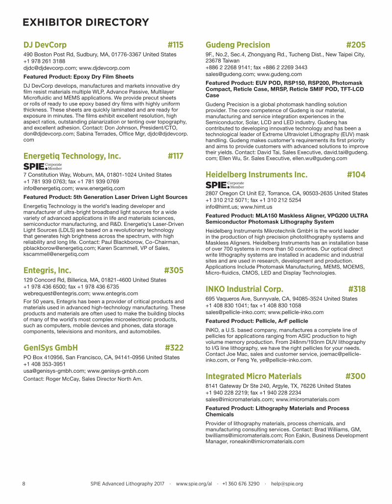
DJ DevCorp #115490BostonPostRd,Sudbury,MA,[email protected];www.djdevcorp.com
Featured Product: Epoxy Dry Film Sheets
DJDevCorpdevelops,manufacturesandmarketsinnovativedryfilmresistmaterialsmultipleWLP,AdvancePassive,MultilayerMicrofluidicandMEMSapplications.Weprovideprecutsheetsorrollsofreadytouseepoxybaseddryfilmswithhighlyuniformthickness.Thesesheetsarequicklylaminatedandarereadyforexposureinminutes.Thefilmsexhibitexcellentresolution,highaspectratios,outstandingplanarizationortentingovertopography,andexcellentadhesion.Contact:DonJohnson,President/CTO,[email protected];SabinaTerrades,OfficeMgr,[email protected]
Energetiq Technology, Inc. #117
7ConstitutionWay,Woburn,MA,01801-1024UnitedStates+17819390763;[email protected];www.energetiq.com
Featured Product: 5th Generation Laser Driven Light Sources
EnergetiqTechnologyistheworld’sleadingdeveloperandmanufacturerofultra-brightbroadbandlightsourcesforawidevarietyofadvancedapplicationsinlifeandmaterialssciences,semiconductormanufacturing,andR&D.Energetiq’sLaser-DrivenLightSources(LDLS)arebasedonarevolutionarytechnologythatgenerateshighbrightnessacrossthespectrum,withhighreliabilityandlonglife.Contact:PaulBlackborow,Co-Chairman,[email protected];KarenScammell,VPofSales,[email protected]
Entegris, Inc. #305129ConcordRd,Billerica,MA,01821-4600UnitedStates+19784366500;[email protected];www.entegris.comFor50years,Entegrishasbeenaproviderofcriticalproductsandmaterialsusedinadvancedhigh-technologymanufacturing.Theseproductsandmaterialsareoftenusedtomakethebuildingblocksofmanyoftheworld’smostcomplexmicroelectronicproducts,suchascomputers,mobiledevicesandphones,datastoragecomponents,televisionsandmonitors,andautomobiles.
GenISys GmbH #322POBox410956,SanFrancisco,CA,[email protected];www.genisys-gmbh.comContact:RogerMcCay,SalesDirectorNorthAm.
Gudeng Precision #2059F.,No.2,Sec.4,ZhongyangRd.,TuchengDist.,NewTaipeiCity,23678Taiwan+886222689141;[email protected];www.gudeng.com
Featured Product: EUV POD, RSP150, RSP200, Photomask Compact, Reticle Case, MRSP, Reticle SMIF POD, TFT-LCD Case
GudengPrecisionisaglobalphotomaskhandlingsolutionprovider.ThecorecompetenceofGudengisourmaterial,manufacturingandserviceintegrationexperiencesintheSemiconductor,Solar,LCDandLEDindustry.GudenghascontributedtodevelopinginnovativetechnologyandhasbeenatechnologicalleaderofExtremeUltravioletLithography(EUV)maskhandling.Gudengmakescustomer’srequirementsitsfirstpriorityandaimstoprovidecustomerswithadvancedsolutionstoimprovetheiryields.Contact:DavidTai,SalesExecutive,[email protected];EllenWu,Sr.SalesExecutive,[email protected]
Heidelberg Instruments Inc. #104
2807OregonCtUnitE2,Torrance,CA,90503-2635UnitedStates+13102125071;[email protected];www.himt.us
Featured Product: MLA150 Maskless Aligner, VPG200 ULTRA Semiconductor Photomask Lithography System
HeidelbergInstrumentsMikrotechnikGmbHistheworldleaderintheproductionofhighprecisionphotolithographysystemsandMasklessAligners.HeidelbergInstrumentshasaninstallationbaseofover700systemsinmorethan50countries.Ouropticaldirectwritelithographysystemsareinstalledinacademicandindustrialsitesandareusedinresearch,developmentandproduction.ApplicationsIncludePhotomaskManufacturing,MEMS,MOEMS,Micro-fluidics,CMOS,LEDandDisplayTechnologies.
INKO Industrial Corp. #318695VaquerosAve,Sunnyvale,CA,94085-3524UnitedStates+14088301041;[email protected];www.pellicle-inko.com
Featured Product: Pellicle, ArF pellicle
INKO,aU.S.basedcompany,manufacturesacompletelineofpelliclesforapplicationsrangingfromASICproductiontohighvolumememoryproduction.From248nm/193nmDUVlithographytoI/Glinelithography,wehavetherightpelliclesforyourneeds.ContactJoeMac,salesandcustomerservice,[email protected],orFengYe,[email protected].
Integrated Micro Materials #3008141GatewayDrSte240,Argyle,TX,76226UnitedStates+19402282219;[email protected];www.imicromaterials.com
Featured Product: Lithography Materials and Process Chemicals
Provideroflithographymaterials,processchemicals,andmanufacturingconsultingservices.Contact:BradWilliams,GM,[email protected];RonEakin,BusinessDevelopmentManager,[email protected]

Onsite News: www.spie.org/ALnews · #SPIElitho 9
EXHIBITOR DIRECTORY
J.A. Woollam #126645MStSte102,Lincoln,NE,68508-2243UnitedStates+14024777501;[email protected];www.jawoollam.comForallyourellipsometryneeds,frommeasuringyourthinfilmsampletotheinstallationandtrainingofyourveryownellipsometer,theJ.A.WoollamCompanyishereforyoueverystepoftheway.Contactustodaytolearnmoreaboutthevarietyofspectroscopicellipsometersweprovidetohelpyoucharacterizeyourthinfilms.Emailustodayatsales@jawoollam.comorvisitusonthewebatwww.jawoollam.com
JENOPTIK Optical Systems, LLC #106
16490InnovationDr,Jupiter,FL,33478-6428UnitedStates+15618817400;[email protected];www.jenoptik-inc.comJENOPTIKOpticalSystemsdeliversauniquerangeofcustomopticalsolutionsrangingfromprecisionassembliestowaferscalemicroopticsandinmaterialsrangingfromglasses,tocrystalsandpolymers.Competenciesincludeopticaltest,opticalpolishing,diamondturningandlithographicetchingofmaterialsforapplicationscoveringDUVtoLWIR.WecombinedesignandengineeringwithhighvolumemanufactureatUSandGlobalmanufacturingsitesinGermanyandIsrael.Contact:RayMalcom,VPSales&Marketing,[email protected];KadeidraWard,InsideSales,[email protected]
JEOL USA Inc. #201
11DearbornRd,Peabody,MA,01960-3823UnitedStates+19785355900;[email protected];www.jeolusa.comJEOL’sportfolioofinnovativesolutionsforthesemiconductorindustryincludesthewidestrangeofe-beamlithographysystemsforavarietyofnextgenerationapplicationsidealforbothuniversityandR&Dlabs.Fromadvancedhigh-endproductionmaskwriterstohigh-precision,direct-writesystems.JEOL’s50yearsofe-beamexperienceprovidescustomerswithunsurpassedtechnicalreliabilityandserviceexpertise.Contact:ZaneMarek,SEProductMgr.,[email protected]
SPONSOR
JSR Micro, Inc. #122
1280NMathildaAve,Sunnyvale,CA,94089-1213UnitedStates+14085438800;fax+14085438996www.jsrmicro.com
Featured Product: Leading-edge photoresists, developers, packaging materials and specialty chemicals.
JSRMicro,Inc.isaninnovationpartnertoitscustomersmanufacturingtheindustry’smostinnovativefamilyofphotoresists,developers,andspecialtychemicals.JSRisalsoaleaderinAdvancedCleansTechnologyandmaterialsforpackaging.OuruniqueTHBseriesofnegativetoneresistsandWPRseriesofdielectricmaterialsareidealfornextgenerationpackagingtechnologiesthatfacilitatehigherperformance.Contact:RichRennels,[email protected];JoeRitter,[email protected]
LouwersHanique #320Energieweg3A,Hapert,5527AHNetherlands+31497339696;[email protected];www.louwershanique.com
Featured Product: 3D components in glass and fused silica using “Selective Laser-induced Etching” (SLE) Technologies
LouwersHaniquehasbeenaleadingspecialistinthemanufacturingoftechnicalglassandceramiccomponentsaswellasassemblytechnologiesforawidevarietyofhigh-techindustriesforover60years.Wearespecializedinthermalformingofglassandinthemechanicalandlaserprocessingoftechnicalglassandtechnicalceramics.Ourstateoftheartequipmentandcleanroomfacilitiesallowtheprecisionmanufacturingofpartsandassemblieswithtolerancesintothe(sub)micronregion.Contact:CarelvandeBeek,SalesManager,[email protected];PaulMeyer,SeniorApplicationsandSalesEngineer,[email protected]
SPONSOR
Mentor Graphics #221
8005SWBoeckmanRd,Wilsonville,OR,97070-7777UnitedStates+15036857000;[email protected];www.mentor.comThechallengesofdevelopingadvancedlithographyflowsrequireastrongpartner.Withacompletedesign-to-manufacturingplatformforImmersionLithography,EUVandDSA,MentorGraphicsistheidealpartnerforsemiconductormanufacturingsuccess.Weofferbest-in-classtechnology,comprehensivesolutions,developmentandproductionsupport,andcontinuousinnovation.Thatiswhymorethan30fabschooseMentorastheirpartner.Getmoreinfoatwww.mentor.com.
SPONSOR
Micro Lithography, Inc. #3271257ElkoDr,Sunnyvale,CA,94089-2211UnitedStates+14087471769;fax+14087471978www.mliusa.com
Featured Product: Pellicles and Mounting Tool
MLIisfeaturingpelliclesformulatedtoyieldhighratesoftransmissionandlonglifetimesforUVexposure.Ourcompletelineofpelliclefilmsrangesfromg-/i-linetoDUV(KrF-248nmandArF-193nm).MLI’sDUVpellicleshavethelowestoutgassingmaterialsavailableinthemarkettoday.Contact:KevinDuong,CustomerServiceManager,[email protected];DianaTjin,SalesAdministrativeManager,[email protected]
micro resist technology GmbH #225KöpenickerStr325,Berlin,12555Germany+4930641670100;[email protected];www.microresist.de
Featured Product: photoresist, photopolymers, nanoimprint resists, hybrid polymers, greyscale resists, inkjet resists
Formorethan20years,microresisttechnologyGmbHhasbeendeveloping,manufacturingandsellinginnovativephotoresists,specialpolymersandancillarymaterialsformicro-andnanolithographyapplications.Duetoourhighlyspecializedproducts,weareatrustedsupplierofglobalhigh-techmarketssuchassemiconductorindustry,MEMS,optoelectronics,nanotechnologyandotheremergingtechnologies.Contact:ArneSchleunitz,ChiefTechnologyOfficer,[email protected]
10 SPIE Advanced Lithography 2017 · www.spie.org/al · +1 360 676 3290 · [email protected]
EXHIBITOR DIRECTORY
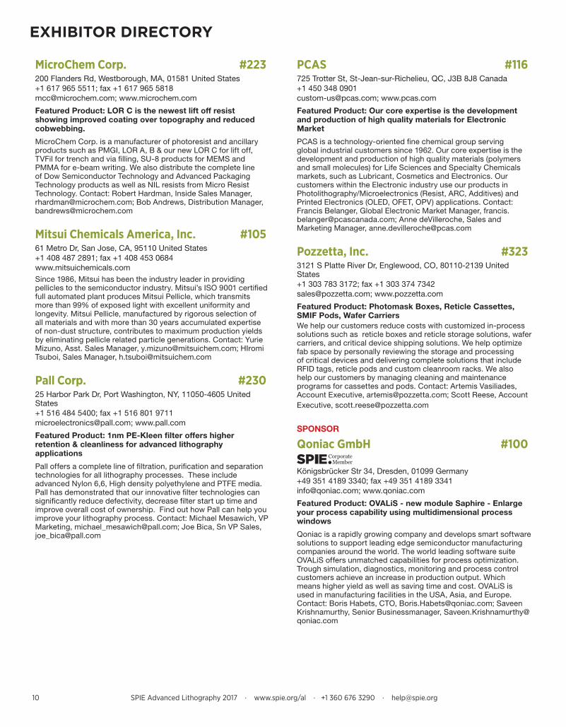
MicroChem Corp. #223200FlandersRd,Westborough,MA,01581UnitedStates+16179655511;[email protected];www.microchem.com
Featured Product: LOR C is the newest lift off resist showing improved coating over topography and reduced cobwebbing.
MicroChemCorp.isamanufacturerofphotoresistandancillaryproductssuchasPMGI,LORA,B&ournewLORCforliftoff,TVFilfortrenchandviafilling,SU-8productsforMEMSandPMMAfore-beamwriting.WealsodistributethecompletelineofDowSemiconductorTechnologyandAdvancedPackagingTechnologyproductsaswellasNILresistsfromMicroResistTechnology.Contact:RobertHardman,InsideSalesManager,[email protected];BobAndrews,DistributionManager,[email protected]
Mitsui Chemicals America, Inc. #10561MetroDr,SanJose,CA,95110UnitedStates+14084872891;fax+14084530684www.mitsuichemicals.comSince1986,Mitsuihasbeentheindustryleaderinprovidingpelliclestothesemiconductorindustry.Mitsui’sISO9001certifiedfullautomatedplantproducesMitsuiPellicle,whichtransmitsmorethan99%ofexposedlightwithexcellentuniformityandlongevity.MitsuiPellicle,manufacturedbyrigorousselectionofallmaterialsandwithmorethan30yearsaccumulatedexpertiseofnon-duststructure,contributestomaximumproductionyieldsbyeliminatingpelliclerelatedparticlegenerations.Contact:YurieMizuno,Asst.SalesManager,[email protected];HIromiTsuboi,SalesManager,[email protected]
Pall Corp. #23025HarborParkDr,PortWashington,NY,11050-4605UnitedStates+15164845400;[email protected];www.pall.com
Featured Product: 1nm PE-Kleen filter offers higher retention & cleanliness for advanced lithography applications
Palloffersacompletelineoffiltration,purificationandseparationtechnologiesforalllithographyprocesses.TheseincludeadvancedNylon6,6,HighdensitypolyethyleneandPTFEmedia.Pallhasdemonstratedthatourinnovativefiltertechnologiescansignificantlyreducedefectivity,decreasefilterstartuptimeandimproveoverallcostofownership.FindouthowPallcanhelpyouimproveyourlithographyprocess.Contact:MichaelMesawich,VPMarketing,[email protected];JoeBica,SnVPSales,[email protected]
PCAS #116725TrotterSt,St-Jean-sur-Richelieu,QC,[email protected];www.pcas.com
Featured Product: Our core expertise is the development and production of high quality materials for Electronic Market
PCASisatechnology-orientedfinechemicalgroupservingglobalindustrialcustomerssince1962.Ourcoreexpertiseisthedevelopmentandproductionofhighqualitymaterials(polymersandsmallmolecules)forLifeSciencesandSpecialtyChemicalsmarkets,suchasLubricant,CosmeticsandElectronics.OurcustomerswithintheElectronicindustryuseourproductsinPhotolithography/Microelectronics(Resist,ARC,Additives)andPrintedElectronics(OLED,OFET,OPV)applications.Contact:FrancisBelanger,GlobalElectronicMarketManager,[email protected];AnnedeVilleroche,SalesandMarketingManager,[email protected]
Pozzetta, Inc. #3233121SPlatteRiverDr,Englewood,CO,80110-2139UnitedStates+13037833172;[email protected];www.pozzetta.com
Featured Product: Photomask Boxes, Reticle Cassettes, SMIF Pods, Wafer CarriersWehelpourcustomersreducecostswithcustomizedin-processsolutionssuchasreticleboxesandreticlestoragesolutions,wafercarriers,andcriticaldeviceshippingsolutions.WehelpoptimizefabspacebypersonallyreviewingthestorageandprocessingofcriticaldevicesanddeliveringcompletesolutionsthatincludeRFIDtags,reticlepodsandcustomcleanroomracks.Wealsohelpourcustomersbymanagingcleaningandmaintenanceprogramsforcassettesandpods.Contact:ArtemisVasiliades,AccountExecutive,[email protected];ScottReese,AccountExecutive,[email protected]
SPONSOR
Qoniac GmbH #100
KönigsbrückerStr34,Dresden,01099Germany+4935141893340;[email protected];www.qoniac.com
Featured Product: OVALiS - new module Saphire - Enlarge your process capability using multidimensional process windows
Qoniacisarapidlygrowingcompanyanddevelopssmartsoftwaresolutionstosupportleadingedgesemiconductormanufacturingcompaniesaroundtheworld.TheworldleadingsoftwaresuiteOVALiSoffersunmatchedcapabilitiesforprocessoptimization.Troughsimulation,diagnostics,monitoringandprocesscontrolcustomersachieveanincreaseinproductionoutput.Whichmeanshigheryieldaswellassavingtimeandcost.OVALiSisusedinmanufacturingfacilitiesintheUSA,Asia,andEurope.Contact:BorisHabets,CTO,[email protected];SaveenKrishnamurthy,SeniorBusinessmanager,[email protected]
Onsite News: www.spie.org/ALnews · #SPIElitho 11
EXHIBITOR DIRECTORY
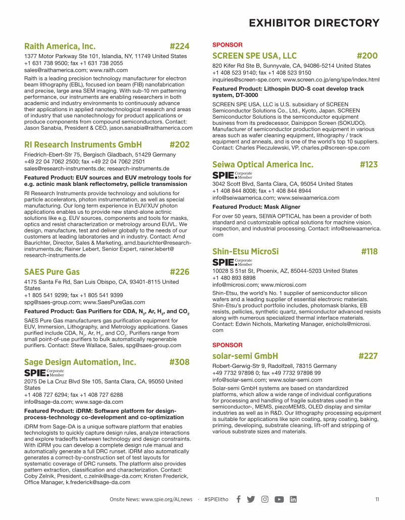
Raith America, Inc. #2241377MotorParkwaySte101,Islandia,NY,11749UnitedStates+16317389500;[email protected];www.raith.comRaithisaleadingprecisiontechnologymanufacturerforelectronbeamlithography(EBL),focusedionbeam(FIB)nanofabricationandprecise,largeareaSEMimaging.Withsub-10nmpatterningperformance,ourinstrumentsareenablingresearchersinbothacademicandindustryenvironmentstocontinuouslyadvancetheirapplicationsinappliednanotechnologicalresearchandareasofindustrythatusenanotechnologyforproductapplicationsorproducecomponentsfromcompoundsemiconductors.Contact:JasonSanabia,President&CEO,[email protected]
RI Research Instruments GmbH #202Friedrich-Ebert-Str75,BergischGladbach,51429Germany+49220470622500;[email protected];research-instruments.de
Featured Product: EUV sources and EUV metrology tools for e.g. actinic mask blank reflectometry, pellicle transmission
RIResearchInstrumentsprovidetechnologyandsolutionsforparticleaccelerators,photoninstrumentation,aswellasspecialmanufacturing.OurlongtermexperienceinEUV/XUVphotonapplicationsenablesustoprovidenewstand-aloneactinicsolutionslikee.g.EUVsources,componentsandtoolsformasks,opticsandresistcharacterizationormetrologyaroundEUVL.Wedesign,manufacture,testanddelivergloballytotheneedsofourcustomersatleadinglaboratoriesandinindustry.Contact:ArndBaurichter,Director,Sales&Marketing,[email protected];RainerLebert,SeniorExpert,[email protected]
SAES Pure Gas #2264175SantaFeRd,SanLuisObispo,CA,93401-8115UnitedStates+18055419299;[email protected];www.SaesPureGas.com
Featured Product: Gas Purifiers for CDA, N2, Ar, H2, and CO2
SAESPureGasmanufacturersgaspurificationequipmentforEUV,Immersion,Lithography,andMetrologyapplications.GasespurifiedincludeCDA,N2,Ar,H2,andCO2.Purifiersrangefromsmallpoint-of-usepurifierstobulkautomaticallyregenerablepurifiers.Contact:SteveWallace,Sales,[email protected]
Sage Design Automation, Inc. #308
2075DeLaCruzBlvdSte105,SantaClara,CA,95050UnitedStates+14087276294;[email protected];www.sage-da.com
Featured Product: iDRM: Software platform for design-process-technology co-development and co-optimization
iDRMfromSage-DAisauniquesoftwareplatformthatenablestechnologiststoquicklycapturedesignrules,analyzeinteractionsandexploretradeoffsbetweentechnologyanddesignconstraints.WithiDRMyoucandevelopacompletedesignrulemanualandautomaticallygenerateafullDRCrunset.iDRMalsoautomaticallygeneratesacorrect-by-constructionsetoftestlayoutsforsystematiccoverageofDRCrunsets.Theplatformalsoprovidespatternextraction,classificationandcharacterization.Contact:CobyZelnik,President,[email protected];KristenFrederick,OfficeManager,[email protected]
SPONSOR
SCREEN SPE USA, LLC #200820KiferRdSteB,Sunnyvale,CA,94086-5214UnitedStates+14085239140;[email protected];www.screen.co.jp/eng/spe/index.html
Featured Product: Lithospin DUO-S coat develop track system, DT-3000
SCREENSPEUSA,LLCisU.S.subsidiaryofSCREENSemiconductorSolutionsCo.,Ltd.,Kyoto,Japan.SCREENSemiconductorSolutionsisthesemiconductorequipmentbusinessfromitspredecessor,DainipponScreen(SOKUDO).Manufacturerofsemiconductorproductionequipmentinvariousareassuchaswafercleaningequipment,lithography/trackequipmentandanneals,andisoneoftheworld’stop10suppliers.Contact:CharlesPieczulewski,VP,[email protected]
Seiwa Optical America Inc. #123
3042ScottBlvd,SantaClara,CA,95054UnitedStates+14088448008;[email protected];www.seiwaamerica.com
Featured Product: Mask Aligner
Forover50years,SEIWAOPTICALhasbeenaproviderofbothstandardandcustomizableopticalsolutionsformachinevision,inspection,andindustrialprocessing.Contact:[email protected]
Shin-Etsu MicroSi #118
10028S51stSt,Phoenix,AZ,[email protected];www.microsi.comShin-Etsu,theworld’sNo.1supplierofsemiconductorsiliconwafersandaleadingsupplierofessentialelectronicmaterials.Shin-Etsu’sproductportfolioincludes,photomaskblanks,EBresists,pellicles,syntheticquartz,semiconductoradvancedresistsalongwithnumerousspecializedthermalinterfacematerials.Contact:EdwinNichols,MarketingManager,[email protected]
SPONSOR
solar-semi GmbH #227Robert-Gerwig-Str9,Radolfzell,78315Germany+497732978980;[email protected];www.solar-semi.comSolar-semiGmbHsystemsarebasedonstandardizedplatforms,whichallowawiderangeofindividualconfigurationsforprocessingandhandlingoffragilesubstratesusedinthesemiconductor-,MEMS,piezoMEMS,OLEDdisplayandsimilarindustriesaswellasinR&D.Ourlithographyprocessingequipmentissuitableforapplicationslikespincoating,spraycoating,baking,priming,developing,substratecleaning,lift-offandstrippingofvarioussubstratesizesandmaterials.

12 SPIE Advanced Lithography 2017 · www.spie.org/al · +1 360 676 3290 · [email protected]
EXHIBITOR DIRECTORY
Solid State Technology #103178618thSt,SanFrancisco,CA,94107UnitedStates+14152550390;[email protected];www.solid-state.com
Featured Product: Solid State Technology Magazine
SolidStateTechnologyreachesthelargest,mostqualifiedcommunityofdecisionmakersforsemiconductorandelectronicsmanufacturingthroughthemagazine,emailnewsletters,website,webcastsandTheConFabConference&Networkingevent.TopicsincludeAdvancedPackaging,MEMS,LEDs,DisplaysandMaterialsaswellascurrenttrendsintheindustry.Visitusherewww.solid-state.com.Contact:KerryHoffman,AssociatePublisher,[email protected]
Synopsys, Inc. #206
690EMiddlefieldRd,MountainView,CA,94043UnitedStates+16505845000;[email protected];www.synopsys.com
Featured Product: Proteus ILT, Proteus LRC, CATS, Sentaurus Lithography
Synopsysprovidesindustry-provenEDAsolutionstomeetthedemandsoftoday’sadvancedICmanufacturingprocesseswhilesettingthestandardinplatformflexibilitytoenableinnovativesolutionsfornextgenerationtechnologynodes.Synopsys’comprehensiveMaskSynthesis,MaskDataPreparation,TCADandYieldManagementtoolsprovideleading-edgeperformance,accuracy,quality,andcostofownershipforallyourproductionanddevelopmentneeds.Contact:[email protected]
SPONSOR
Tokyo Electron #1302400GroveBlvd,Austin,TX,78741-6500UnitedStates+15127508219;fax+15124241001www.tel.com
Featured Product: Coaters / developers for 100 - 450mm substrates including masks
TokyoElectron(TEL)isaleadingglobalsupplierofinnovativesemiconductorandflatpaneldisplayproductionequipment.Productlinesincludecoater/developers,thermalprocessingsystems,plasmaetchers,singlewaferdepositionsystems,surfacepreparationsystemsandotherequipmentsupportingthemanufacturingandtestingofsemiconductors.Focusedonproductivityandcostofownership,TELoffersadvancedlithographicprocessandhardwaresolutionsfor7nmnodesandbeyond.Contact:RobCrowell,ProductMarketingManager,[email protected];KatyCrist,MarketingCommunicationsManager,[email protected]
SPONSOR
Tokyo Ohka Kogyo America, Inc. #211190TopazSt,Milpitas,CA,95035-5429UnitedStates+14089569901;[email protected];www.tokamerica.com
Featured Product: EUV, DSA, Arf Immersion, ArF, KrF, i-Line, g-Line photoresists and supporting chemistries.
TOKAmericamanufacturesandmarketsultrahighpurityphotoresistsandauxiliarychemicalsusedinthefabricationofintegratedcircuits.TOKAmericaisaUSsubsidiaryofTokyoOhkaKogyoCo.,Ltd.,inKawasaki,Japan,aworldleaderinthemanufactureofphotoresists,auxiliaryliquidchemicalproducts,andprocessequipmentforthesemiconductorcircuit,semiconductorpackaging,imagesensor/MEMS,3Dpackaginganddisplaytechnologymaterialsindustry.Contact:AaronVickery,SeniorAccountManagerBusinessDevelopment,[email protected]
Vistec Electron Beam GmbH #213Ilmstr4,Jena,07743Germany+49364179980;[email protected];www.vistec-semi.com
Featured Product: Vistec SB3050 series & Vistec SB250 series - variable shaped beam systems
VistecElectronBeamGmbHprovidesleadingtechnologysolutionsforadvancedelectron-beamlithography.BasedontheVariableShapedBeam(VSB)principle,theelectron-beamlithographysystemsaremainlyutilizedforsemiconductorapplicationsandadvancedresearchassilicondirectwrite,compoundsemiconductor,maskmakingaswellasintegratedopticsandseveralnewemergingmarkets.ThecompanyislocatedinJena,Germanyandmaintainsservice&supportcentersinEurope,Taiwan&intheUS.Contact:InesStolberg,ManagerProductManagement&Marketing,[email protected];KevinGrens,BusinessDevelopmentManager,[email protected]
Zygo Corporation #207
21LaurelBrookRd,Middlefield,CT,06455-1291UnitedStates+18603478506;[email protected];www.zygo.comZYGOisaworldwidesupplierofopticalmetrologyinstruments,precisionoptics,andelectro-opticaldesignandmanufacturingservices,providingproductivityandyieldimprovementsolutionsforavarietyofindustries.ZYGOprovidesawiderangeofinspection,surfaceanalysis,andprecisiondisplacementmeasurementsolutions,aswellasprecisionoptics,opticaldesign,andopto-mechanicalassembly.ZYGOwillbeexhibitingtheirnewestlinesofmetrologysystemsandopticalcapabilities.Contact:DavidMelton,DirectorSales&Support,[email protected];MarcTricard,DivisionVPOptics,mtricard2zygo.com
Onsite News: www.spie.org/ALnews · #SPIElitho 13
PRODUCT CATEGORIES
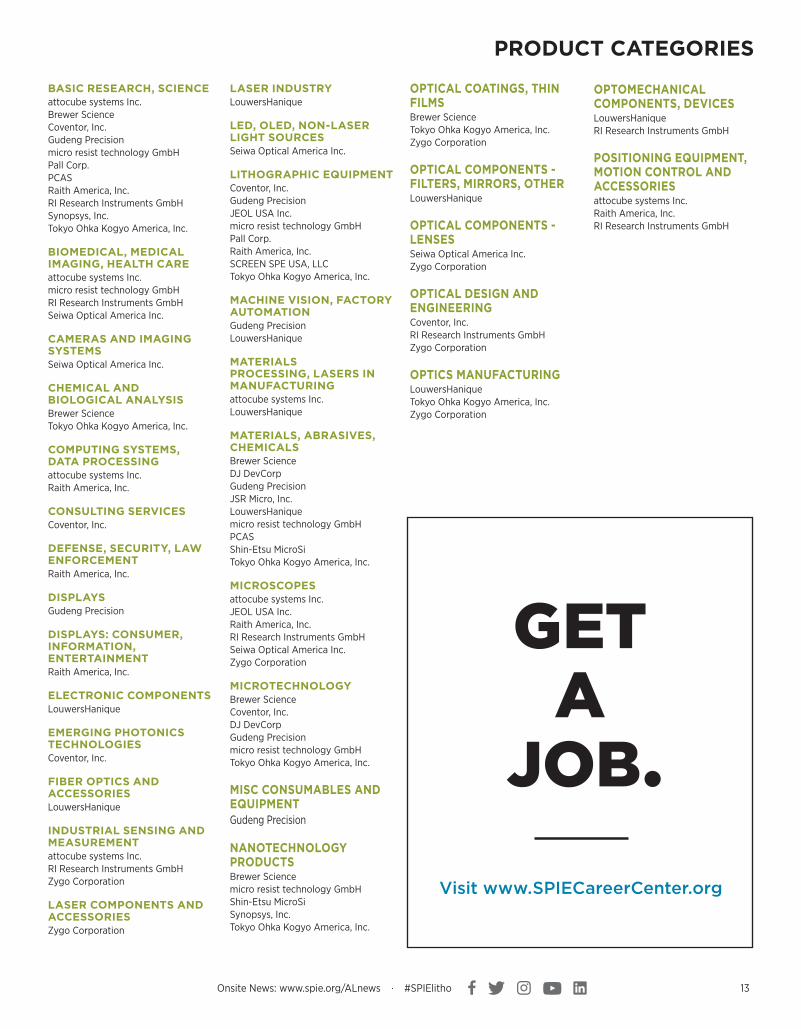
BASIC RESEARCH, SCIENCEattocube systems Inc.Brewer ScienceCoventor, Inc.Gudeng Precisionmicro resist technology GmbHPall Corp.PCASRaith America, Inc.RI Research Instruments GmbHSynopsys, Inc.Tokyo Ohka Kogyo America, Inc.
BIOMEDICAL, MEDICAL IMAGING, HEALTH CAREattocube systems Inc.micro resist technology GmbHRI Research Instruments GmbHSeiwa Optical America Inc.
CAMERAS AND IMAGING SYSTEMSSeiwa Optical America Inc.
CHEMICAL AND BIOLOGICAL ANALYSISBrewer ScienceTokyo Ohka Kogyo America, Inc.
COMPUTING SYSTEMS, DATA PROCESSINGattocube systems Inc.Raith America, Inc.
CONSULTING SERVICESCoventor, Inc.
DEFENSE, SECURITY, LAW ENFORCEMENTRaith America, Inc.
DISPLAYSGudeng Precision
DISPLAYS: CONSUMER, INFORMATION, ENTERTAINMENTRaith America, Inc.
ELECTRONIC COMPONENTSLouwersHanique
EMERGING PHOTONICS TECHNOLOGIESCoventor, Inc.
FIBER OPTICS AND ACCESSORIESLouwersHanique
INDUSTRIAL SENSING AND MEASUREMENTattocube systems Inc.RI Research Instruments GmbHZygo Corporation
LASER COMPONENTS AND ACCESSORIESZygo Corporation
LASER INDUSTRYLouwersHanique
LED, OLED, NON-LASER LIGHT SOURCESSeiwa Optical America Inc.
LITHOGRAPHIC EQUIPMENTCoventor, Inc.Gudeng PrecisionJEOL USA Inc.micro resist technology GmbHPall Corp.Raith America, Inc.SCREEN SPE USA, LLCTokyo Ohka Kogyo America, Inc.
MACHINE VISION, FACTORY AUTOMATIONGudeng PrecisionLouwersHanique
MATERIALS PROCESSING, LASERS IN MANUFACTURINGattocube systems Inc.LouwersHanique
MATERIALS, ABRASIVES, CHEMICALSBrewer ScienceDJ DevCorpGudeng PrecisionJSR Micro, Inc.LouwersHaniquemicro resist technology GmbHPCASShin-Etsu MicroSiTokyo Ohka Kogyo America, Inc.
MICROSCOPESattocube systems Inc.JEOL USA Inc.Raith America, Inc.RI Research Instruments GmbHSeiwa Optical America Inc.Zygo Corporation
MICROTECHNOLOGYBrewer ScienceCoventor, Inc.DJ DevCorpGudeng Precisionmicro resist technology GmbHTokyo Ohka Kogyo America, Inc.
MISC CONSUMABLES AND EQUIPMENTGudeng Precision
NANOTECHNOLOGY PRODUCTSBrewer Sciencemicro resist technology GmbHShin-Etsu MicroSiSynopsys, Inc.Tokyo Ohka Kogyo America, Inc.
OPTICAL COATINGS, THIN FILMSBrewer ScienceTokyo Ohka Kogyo America, Inc.Zygo Corporation
OPTICAL COMPONENTS - FILTERS, MIRRORS, OTHERLouwersHanique
OPTICAL COMPONENTS - LENSESSeiwa Optical America Inc.Zygo Corporation
OPTICAL DESIGN AND ENGINEERINGCoventor, Inc.RI Research Instruments GmbHZygo Corporation
OPTICS MANUFACTURINGLouwersHaniqueTokyo Ohka Kogyo America, Inc.Zygo Corporation
GET A
JOB•
Visit www.SPIECareerCenter.org
OPTOMECHANICAL COMPONENTS, DEVICESLouwersHaniqueRI Research Instruments GmbH
POSITIONING EQUIPMENT, MOTION CONTROL AND ACCESSORIESattocube systems Inc.Raith America, Inc.RI Research Instruments GmbH

14 SPIE Advanced Lithography 2017 · www.spie.org/al · +1 360 676 3290 · [email protected]
SPIE EVENT POLICIES
Acceptance of Policies and Registration ConditionsThe following Policies and Conditions apply to all SPIE Events. As a condition of registration, you will be required to acknowledge and accept the SPIE Registration Policies and Conditions contained herein.
IdentificationTo verify registered participants and provide a measure of security, SPIE will ask attendees to present a government-issued Photo ID at registra-tion to collect registration materials.
Individuals are not allowed to pick up badges for attendees other than themselves. Further, attendees may not have some other person par-ticipate in their place at any conference-related activity. Such other in-dividuals will be required to register on their own behalf to participate.
Access to Technical and Networking Events All technical and networking events require a conference badge for admission. Registered attendees may bring their children with them as long as everyone is badged. Registration badges for children under 18 are free and available at the SPIE registration desk onsite. Children un-der 14 years of age must be accompanied by an adult at all times, and guardians are asked to help maintain a professional, disturbance-free conference environment.
Exhibition Hall Policy Everyone who attends the exhibition must be registered and have a badge. Badges for children are free and available onsite at the registra-tion desk. Children under 14 years of age must be accompanied by an adult at all times. Guardians are asked to help maintain a professional, disturbance-free exhibition environment. For safety and insurance rea-sons, children under 18 are not allowed in the exhibition area during ex-hibition move-in and move-out.
Payment MethodRegistrants for paid elements of the event, who do not provide a method of payment, will not be able to complete their registration. Individuals with incomplete registrations will not be able to attend the conference until payment has been made. SPIE accepts VISA, MasterCard, Ameri-can Express, Discover, Diner’s Club, checks and wire transfers. Onsite registrations can also pay with Cash.
Authors/CoauthorsBy submitting an abstract, you agree to the following conditions:
• An author or coauthor (including keynote, invited, and solicited speak-ers) will register at the author registration rate, attend the meeting, and make the presentation as scheduled.
• A manuscript (minimum 6 pages, maximum 20 pages) for any accepted oral, invited, keynote, or poster presentation will be submitted for publication in the Proceedings of SPIE in the SPIE Digital Library. Some SPIE events have other requirements that the author is made aware of at the time of submission.
Granting Attendee Registration and AdmissionSPIE, or their officially designated event management, in their sole dis-cretion, reserves the right to accept or decline an individual’s registra-tion for an event. Further, SPIE, or event management, reserves the right to prohibit entry or remove any individual whether registered or not, be they attendees, exhibitors, representatives, or vendors, who in their sole opinion are not, or whose conduct is not, in keeping with the char-acter and purpose of the event. Without limiting the foregoing, SPIE and event management reserve the right to remove or refuse entry to any attendee, exhibitor, representative, or vendor who has registered or gained access under false pretenses, provided false information, or for any other reason whatsoever that they deem is cause under the cir-cumstances.
SPIE Safe Meeting and Misconduct PolicySPIE is a professional, not-for-profit society committed to providing valuable and safe conference and exhibition experiences. SPIE is dedi-cated to equal opportunity and treatment for all its members, meet-ing attendees, staff, and contractors. Attendees are expected to be respectful to other attendees, SPIE staff, and contractors. Harassment and other misconduct will not be tolerated; violators will be addressed promptly and seriously. Consequences up to and including expulsion from the event as appropriate will be implemented immediately.
The SPIE anti-harassment policy can be found at http://spie.org/policy.
Reporting of Unethical or Inappropriate BehaviorSPIE is an organization with strong values of responsibility and integrity. Our Harassment Policy, Ethics Statement, and Code of Professional Con-duct contain general guidelines for behavior and for conducting busi-ness with the highest standards of ethics.
Onsite at a SPIE meeting, contact any SPIE Staff member with concerns or questions for thorough follow-up. If you feel in immediate danger, please dial 911 for police intervention.
SPIE has established a confidential reporting system for staff and all meetings participants to raise concerns about possible unethical or in-appropriate behavior within our community. Complaints may be filed by phone at +1-888-818-6898 or at www.SPIE.ethicspoint.com and, if preferred, may be made anonymously.

Onsite News: www.spie.org/ALnews · #SPIElitho 15
Wireless Internet Service Policy At SPIE events where wireless is included with your registration, SPIE provides wireless access for attendees during the conference and exhi-bition but cannot guarantee full coverage in all locations, all of the time. Please be respectful of your time and usage so that all attendees are able to access the internet.
Excessive usage (e.g., streaming video, gaming, multiple devices) re-duces bandwidth and increases cost for all attendees. No routers may be attached to the network. Properly secure your computer before access-ing the public wireless network. Failure to do so may allow unauthorized access to your laptop as well as potentially introduce viruses to your computer and/or presentation. SPIE is not responsible for computer vi-ruses or other computer damage.
Mobile Phones and Related Devices PolicyMobile phones, tablets, laptops, pagers, and any similar electronic de-vices should be silenced during conference sessions. Please exit the conference room before answering or beginning a phone conversation.
SmokingFor the health and consideration of all attendees, smoking, including e-cigarettes, is not permitted at any event elements, such as but not limited to: plenaries, conferences, workshops, courses, poster sessions, hosted meal functions, receptions, and in the exhibit hall. Most facilities also prohibit smoking and e-cigarettes in all or specific areas. Attendees should obey any signs preventing or authorizing smoking in specified locations.
Hold HarmlessAttendee agrees to release and hold harmless SPIE from any and all claims, demands, and causes of action arising out of or relating to your participation in the event you are registering to participate in and use of any associated facilities or hotels.
Event CancellationIf for some unforeseen reason SPIE should have to cancel the event, registration fees processed will be refunded to registrants. Registrants will be responsible for cancellation of travel arrangements or housing reservations and the applicable fees.
SPIE International HeadquartersPO Box 10
Bellingham, WA 98227-0010 USA
Tel: +1 360 676 3290
Fax: +1 360 647 1445
[email protected] • www.SPIE.org
SPIE Europe Offices2 Alexandra Gate
Ffordd Pengam, Cardiff, CF24 2SA UK
Tel: +44 29 2089 4747
Fax: +44 29 2089 4750
[email protected] • www.SPIE.org
SPIE EVENT POLICIES• Only papers presented at the conference and received according to
publication guidelines and timelines will be published in the Proceed-ings of SPIE in the SPIE Digital Library (or via the requirements of that event).
Audio, Video, Digital Recording PolicyConferences, courses, and poster sessions: For copyright reasons, re-cordings of any kind are prohibited without prior written consent of the presenter or instructor. Attendees may not capture or use the materials presented in any meeting/course room or in course notes on display without written permission. Consent forms are available at Speaker Check-In. Individuals not complying with this policy will be asked to leave a given session and/or asked to surrender their recording media.
EXHIBITION HALL: For security and courtesy reasons, recordings of any kind are prohibited unless one has explicit permission from on-site com-pany representatives. Individuals not complying with this policy will be asked to surrender their recording media and to leave the exhibition hall.
Capture and Use of a Person’s ImageBy registering for an SPIE event, I grant full permission to SPIE to cap-ture, store, use, and/or reproduce my image or likeness by any audio and/or visual recording technique (including electronic/digital pho-tographs or videos), and create derivative works of these images and recordings in any SPIE media now known or later developed, for any legitimate SPIE marketing or promotional purpose.
By registering for an SPIE event, I waive any right to inspect or approve the use of the images or recordings or of any written copy. I also waive any right to royalties or other compensation arising from or related to the use of the images, recordings, or materials. By registering, I release, defend, indemnify and hold harmless SPIE from and against any claims, damages or liability arising from or related to the use of the images, re-cordings or materials, including but not limited to claims of defamation, invasion of privacy, or rights of publicity or copyright infringement, or any misuse, distortion, blurring, alteration, optical illusion or use in com-posite form that may occur or be produced in taking, processing, reduc-tion or production of the finished product, its publication or distribution.
Laser Pointer Safety Information/PolicySPIE supplies tested and safety-approved laser pointers for all confer-ence meeting rooms. For safety reasons, SPIE requests that presenters use provided laser pointers.
Use of a personal laser pointer represents user’s acceptance of liability for use of a non-SPIE-supplied laser pointer. If you choose to use your own laser pointer, it must be tested to ensure <5 mW power output. Laser pointers in Class II and IIIa (<5mW) are eye safe if power output is correct, but output must be verified because manufacturer labeling may not match actual output. Come to Speaker Check-In and test your laser pointer on our power meter. You are required to sign a waiver releasing SPIE of any liability for use of potentially non-safe, personal laser point-ers. Misuse of any laser pointer can lead to eye damage.
Unauthorized Solicitation PolicyUnauthorized solicitation in the Exhibition Hall is prohibited. Any non-exhibiting manufacturer or supplier observed to be distributing information or soliciting business in the aisles, or in another company’s booth, will be asked to leave immediately.
Unsecured Items PolicyPersonal belongings should not be left unattended in meeting rooms or public areas. Unattended items are subject to removal by security. SPIE is not responsible for items left unattended.
16 SPIE Advanced Lithography 2017 · www.spie.org/al · +1 360 676 3290 · [email protected]
THE INTERNATIONAL SOCIETY FOR OPTICS AND PHOTONICS
Through collaboration, companies large and small steer the latest innovations toward practical relevance and revenue in the global marketplace.
SPIE Corporate Membership increases your visibility, adds individual benefits, and provides significant discounts on:
SPIE exhibitions* | SPIE Digital Library subscriptionsAdvertising rates | Mailing lists | Recruitment services
*SPIE Corporate Members receive a 15% discount on exhibit space.
3SAE Technologies, Inc.4D Technology Corp.5N Plus Semiconductors, LLCABB Analytical MeasurementAbet Technologies, Inc.Abrisa TechnologiesAccess Laser Co.AccuStrata Inc.Acktar Ltd.Adimec Electronic Imaging, Inc.AdlOptica Optical Systems GmbHAdmesy B.V.AdTech Ceramics Co.AdTech Optics, Inc.AdValue Photonics, Inc.Advance Reproductions Corp.Advanced Abrasives Corp.Advanced Energy Industries, Inc.Advanced Fiber Resources
(Zhuhai) Ltd.Advanced Microoptic Systems
GmbHAdvanced Optowave Corp.Advanced Power Group Corp.AdvR, Inc.AEMtec GmbHAerotech, Inc.AFLAKELA Laser Corp.Alazar Technologies, Inc.ALIO Industries Corp.Allied Vision Technologies Inc.AllMotion, Inc.AlluxaALPAO S.A.S.Alpine Research OpticsAltechna UABAltos Photonics, Inc.American Photonics Co.AMETEK HCC Industries, Inc.AMETEK Precitech, Inc.AMETEK Taylor Hobson Inc.AMETEK Vision Research®, Inc.AMETEK, Inc.Andover Corp.Aperture Optical Sciences Inc.Applied Image, Inc.Applied Optics Ctr., a Div. of Optex
Systems, Inc.
Applied Optics, Inc.Applied Photonics Inc.Applied Physics & Electronics, Inc.Applied Surface TechnologiesApplied Technology AssociatesÄpre Instruments, LLCApril Electro-Optics Co., Ltd.Archer OpTx, Inc.Arden Photonics Ltd.Arrow Thin Films, Inc.Arroyo Instruments, LLCASA Astrosysteme GmbHAsahi Spectra USA Inc.Ascentta, Inc.asphericon, Inc.ASTRODESIGN, Inc.attocube systems Inc.Avantes, Inc.Avo Photonics, Inc.Ayase America Inc.B&W Tek, Inc.Ball Aerospace & Technologies
Corp.BaySpec, Inc.Beamtech Optronics Co., Ltd.Beijing Scitlion Technology Co.,
Ltd.Berliner Glas KGaA Herbert Kubatz
GmbH & Co.BigC Dino-Lite Digital MicroscopeBiophotonic Solutions, Inc.Blue Ridge Optics, LLCBodkin Design & Engineering, LLCBoston Applied Technologies, Inc.Boston Electronics Corp.Boston Micromachines Corp.Boulder Nonlinear SystemsBoXin Photoelectric Co., Ltd.Brandywine Photonics, LLCBreault Research Organization, Inc.Brewer Science, Inc.Bristol Instruments, Inc.Brolis Semiconductors UABBühler Inc.BWT Beijing Ltd.Calmar LaserCambridge TechnologyCanon U.S.A., Inc.Carl Zeiss, Inc.Cascade Laser Corp.
Cascade Optical Corp.CASTON Inc.CEA-LETIChangchun New Industries
Optoelectronics Technology Co., Ltd.
Chenter Industries Group Ltd.Chiral Photonics, Inc.Chroma Technology Corp.Churchill NavigationCI Systems, Inc.Cirrus Logic, Inc.Clear AlignClemson Univ.Coastal ConnectionsCoherent, Inc.Collimated Holes, Inc.ContinuumContour Metrological &
Manufacturing, Inc.CorActive High-Tech Inc.Coresix Precision Glass, Inc.Covesion Ltd.CPG Optics, Inc.CREOL, The College of Optics
and Photonics, Univ. of Central Florida
Cristal Laser S.A.CryLight Photonics, Inc.Cryslaser Inc.Crystal IS, Inc.CRYSTECH Inc.Cybel LLCDaheng New Epoch Technology,
Inc.DataRay Inc.Daylight Solutions Inc.DCM Tech, Corp.Deltronic Crystal Industries, Inc.Deposition Sciences, Inc.Diamond USA Inc.DIAS Infrared Corp.DiCon Fiberoptics, Inc.DILAS Diode Laser, Inc.DILAS Diodenlaser GmbHDiverse Optics Inc.Docter Optics, Inc.Dominar, Inc.DRS Technologies, Inc.DST CONTROL AB
Dynamic Structures Ltd.DynaVacDZD Photonics Co., Ltd.E.R. Precision Optical Corp.e2v Aerospace and Defense, Inc.e2v technologies plcEdmund Optics Inc.Electro Optical Components, Inc.Electro Optical Industries, Inc.Electro-Optical Imaging, Inc.Electro-Optics Technology, Inc.Elite Optoelectronics Co., Ltd.Elliot Scientific Ltd.EMD Performance Materials Corp.EMF Corp.Eminess Technologies, Inc.Empire Precision PlasticsEmpire West, Inc.Energetiq Technology, Inc.Enplas Microtech, Inc.EPIR Technologies, Inc.EPIX, Inc.Esterline CMC Electronics, Inc.Evaporated Coatings, Inc.EVERIX, Inc.Exalos AGExcelitas QioptiqExcelitas Technologies Corp.Excell TechnologyExciton, Inc.Fantom Materials, Inc.Feinwerkoptik Zünd AGFiber Optic Valley ABFiberCryst S.A.S.Fiberguide Industries, Inc.Fibertech Optica Inc.ficonTEC Service GmbHFirst Light Imaging S.A.S.First Sensor, Inc.FISBA AGFJW Optical Systems, Inc.Flexible Optical B.V.FLIR Systems, Inc.FluxData, Inc.FOCtek Photonics, Inc.Foreal Spectrum, Inc.Fotofab, LLCFrankfurt Laser Co.Fraunhofer UK Research Ltd.

Onsite News: www.spie.org/ALnews · #SPIElitho 17
SPIE CORPORATE MEMBERS
Fraunhofer-Institut für Photonische Mikrosysteme
Fresnel Technologies Inc.Fuzhou Alpha Optics Co., Ltd.Fuzhou Intpho Technology Co., Ltd.GAMDAN OpticsGeneral Dynamics-Global Imaging
TechnologiesGeneral Ruby & Sapphire Co.GenISys IncGentec Electro-Optics Inc.Georgia Tech Research InstituteGlass Fab, Inc.Gooch & Housego PLCGPD Optoelectronics Corp.Greenlight Optics, LLCgreenTEG AGGrintech GmbHGS Plastic OpticsGuernsey Coating Labs., Inc.Gulf Fiberoptics, Inc.Haas Laser Technologies, Inc.Hamamatsu Corp.Hangzhou Techwin Precision
Instrument Co., Ltd.Haphit IncHardin Optical Co.HC Photonics Corp.Headwall Photonics Inc.Heidelberg Instruments Inc.
Hellma USA, Inc.heracle GmbHHeraeus Tenevo LLCHIGHYAG Lasertechnologie GmbHHinds Instruments, Inc.Hindsight Imaging, Inc.Hofstadter Analytical Services, LLCHOLO/OR Ltd.HOLOEYE Photonics AGHolographix LLCHong Kong Productivity CouncilHORIBA Instruments Inc.HOYA Corp. USAHTA PhotomaskHuanic Corp.Ibsen Photonics A/Sibss Group, Inc.IDEX Corp.IDEX Health & Science LLCIDEX Optical TechnologiesII-VI EpiWorks, Inc.II-VI Inc.II-VI InfraredII-VI Laser Enterprise GmbHII-VI MarlowII-VI Optical SystemsIMECIMPERX Inc.IMRA America, Inc.
Incom, Inc.Indian Hills Community CollegeInfinite Optics Inc.Infrared Materials, Inc.Infrared Systems Development
Corp.Infratec Infrared LLCINGENERIC GmbHInnolume GmbHInnovations in Optics, Inc.Innovative Photonic SolutionsINOInPhenix, Inc.Inrad OpticsInsight Photonic Solutions, Inc.Institute for Photonics and
Advanced SensingInternational Consortium for
Advanced Manufacturing Research (ICAMR)
International Optoelectronics, LLCIntlvac Thin FilmIO Industries, Inc.IPG Photonics Corp.IRCAM GmbHIRCameras, LLCIRD GlassIRflex CorporationIris AO, Inc.IRnova AB
IRsweep GmbHIRTronix, Inc.Isomet Corp.ISP Optics Corp.Isuzu Glass, Inc.ITF Technologies Inc.ITW Opto Diode Corp.Janos Technology, LLCJENOPTIK Optical Systems GmbHJENOPTIK Optical Systems, LLCJEOL USA Inc.JSR Micro, Inc.Kappa optronics, Inc.Kapteyn-Murnane Labs., Inc.Kaufman & Robinson, Inc.Kentek Corp.Kigre, Inc.Kiyohara Optics Inc.KrellTechKugler of America Ltd.L-3 Cincinnati Electronics Labsphere, Inc.LaCroix Precision OpticsLambda Research Corp.Lambda Research Optics, Inc.Lanmark Controls Inc.Laser Components USA, Inc.Laser Focus WorldLaser Institute of America
CONNECTING MINDS. ADVANCING LIGHT.
PHOTOMASK TECHNOLOGY + EXTREME ULTRAVIOLET LITHOGRAPHYA technical meeting for mask makers, EUVL, emerging technologies, and the future of mask buisness.
Call for Paperswww.spie.org/pm2017
Monterey, California, USA Conference: 11–14 September 2017 Exhibition: 12–13 September 2017

18 SPIE Advanced Lithography 2017 · www.spie.org/al · +1 360 676 3290 · [email protected]
SPIE CORPORATE MEMBERS
Laser Light Technologies Inc.Laser Quantum Inc.Laser Safety IndustriesLaser-compact Co. Ltd.Laser-FemtoLaserline Inc.Laservision USALASORBLASOS Lasertechnik GmbHLattice Electro Optics, Inc.Lein Applied Diagnostics Ltd.LEONI Fiber Optics, Inc.LightComm Technology Co., Ltd.LightMachinery Inc.LightPath Technologies, Inc.Litron Lasers Ltd.Lockheed Martin AculightLTI Optics, LLCLumencor, Inc.Luna OptoelectronicsLuvantix SSCPLuxel Corp.M Squared Lasers Ltd.M3 Measurement SolutionsMad City Labs., Inc.Mahr-ESDIMarina Photonics, Inc.Market Tech, Inc.Marktech OptoelectronicsMarubeni America Corp.Materion Barr Precision Optics &
Thin Film CoatingsMeadowlark Optics, Inc.MegaWatt Lasers, Inc.Mentor Graphics CorpMesa Photonics, LLCMH GoPower Company LimitedMichigan Photonics ClusterMicro Laser Systems, Inc.MicroCircuit Labs., LLCMicrofine Materials Technologies
Pte Ltd.MICRONIX USA, LLCMicronor Inc.Microtech Instruments, Inc.Mightex SystemsMikro-Tasarim Elektronik San. ve
Tic. A.Ş.Mildex, Inc.Mindrum Precision, Inc.Minus K Technology Inc.Mirrorcle Technologies, Inc.MKS Instruments, Inc.ML Optic Corp.MLD Technologies, LLCMontana Photonics Industry
AllianceMONTFORT Laser GmbHMOXTEK, Inc.MPA Crystal Corp.MPB Communications Inc.Multi IR Optoelectronics Co., Ltd.Multisorb TechnologiesMWTechnologies, LdaNaked Optics Corp.
NANEO Precision IBS Coatings GmbH
nanoplus GmbHnanosystec GmbHNanotronics ImagingNantong Ruisen Optical Element
Technology Co., Ltd.National Aperture, Inc.National Institute of Standards and
TechnologyNational Metrology Ctr.Natsume Optical Corp.Navitar Inc.Necsel IP, Inc.New England Optical SystemsNew England Photoconductor
Corp.New Scale Technologies, Inc.New Source Technology, LLCNewport Corp.Newport Thin Film Lab., Inc.NiCoForm, Inc.nLIGHT Corp.Norland Products Inc.Norlase ApSNorPix Inc.Northrop Grumman Cutting Edge
OptronicsNP Photonics, Inc.nPoint, Inc.NRD Advanced Static ControlNufernNuFlare Technology, Inc.Nutfield TechnologyNüvü Caméras Inc.Ocean Optics, Inc.OEwaves, Inc.OFSOhara Corp.Ondax, Inc.Onefive GmbHOPCO Lab., Inc.Open Photonics, Inc.Optec S.p.A.Optical Filter Source, LLCOptical Support, Inc.Optics BalzersOptics Technology, Inc.Optiforms, Inc.OptiGrate Corp.Optikos Corp.Optilab LLCOptimax Systems, Inc.OptiPro SystemsOptiSource, LLCOptiwave Systems Inc.Opto-Alignment Technology, Inc.Opto-Knowledge Systems, Inc.Opto-Line International, Inc.Optonetic LLCOptores GmbHOptoSigma Corp.Optotune Switzerland AGOptowaves, Inc.OSELA Inc.
OZ Optics Ltd.Pacific Laser EquipmentPangolin Laser Systems, Inc.Pavilion Integration Corp.PCO-TECH Inc.Perkins Precision Developments,
LLCPFG Precision Optics, Inc.PHASICS Corp.Photon DesignPhoton Engineering LLCPhoton etc.Photon Manufacturing, LLCPhotonic Cleaning TechnologiesPhotonics Industries International,
Inc.PHOTONIS USA, Inc.Photop Optics Co., Ltd.Photop Suwtech, Inc.PI (Physik Instrumente) L.P.PicoQuant Photonics North
America, Inc.Pie Photonics Ltd.PIEZOCONCEPTpiezosystem jena, Inc.PIKE TechnologiesPixelteq, Inc.Polaris MotionPovolzhskiy State Univ. of
Telecommunications and Informatics
Precision Glass & OpticsPrecision Glass BendingPrecision OpticalPrinceton InstrumentsPrinceton Lightwave, Inc.Prior Scientific Inc.Prizmatix Ltd.PROMET OpticsPure PhotonicsPVP Advanced EO Systems, Inc.QD Laser, Inc.QED Technologies, Inc.Qoniac GmbHQPC Lasers/Laser Operations LLCQuantel USAQuartus Engineering Inc.Radiant Light SLRaicol Crystals Ltd.Rainbow Research Optics, Inc.Raptor Photonics Ltd.Raytheon ELCAN Optical
TechnologiesRedondo Optics, Inc.RedWave Labs Ltd.Research Electro-Optics, Inc.Reynard Corp.RICOR USA, Inc.Rochester Precision Optics, LLCRocky Mountain Instrument Co.Ross Optical IndustriesRPC Photonics, Inc.RPMC Lasers, Inc.
RSP TechnologyRubicon Technology Inc.Ruda-Cardinal, Inc.Saber 1 TechnologiesSacher Lasertechnik GmbHSafran Optics 1Sage Design Automation, Inc.Salem Distributing Co., Inc.Santa Barbara Infrared, Inc.SantierSatisloh North America Inc.Savvy Optics Corp.SCANLAB America, Inc.ScannerMAXSCD SemiConductor DevicesSCD.USA, LLCSchneider Optical Machines Inc.Schneider Optics, Inc.SCHOTT AGSCHOTT DiamondView Armor
Products, LLCSCHOTT North America, Inc.Scientific Materials Corp.Seattle Photonics Associates LLCSeiwa Optical America Inc.SemiNex Corp.SensL Technologies Ltd.Sensofar-USASensors Unlimited, a United
Technologies Co.SensUpShanghai Jiaguang Optics GroupShanghai Optics Inc.Shasta CrystalsSheaumann Laser, Inc.Shin-Etsu MicroSi, Inc.Sierra Precision OpticsSierra-Olympic Technologies, Inc.Sigmadyne, Inc.Sill Optics GmbH & Co. KGSimera Technology Group Pty Ltd.Siskiyou CorporationSlicingTechSmarAct GmbHSpecim Spectral Imaging Ltd.Spectral Devices Inc.Spectral Instruments, Inc.Spectrogon ABSpectrogon UK Ltd.Spectrogon US, Inc.Spectrum Scientific, Inc.Spectrum Thin Films Corp.Spica Technologies, Inc.SRI International SarnoffStanford Computer Optics, Inc.StellarNet, Inc.Stemmerich, Inc.STFC Rutherford Appleton Lab.Sunny Opotech North America, Inc.Sunny TechnologySutter Instrument Corp.Swamp Optics, LLCSwissLitho AG

Onsite News: www.spie.org/ALnews · #SPIElitho 19
SPIE CORPORATE MEMBERS
Sydor Optics, Inc.Synopsys, Inc.Syntec OpticsTAG Optics, Inc.tec5USA, Inc.Technical Manufacturing Corp.Technische Informationsbibliothek
(TIB)TecOptics, Inc.Tecport Optics, Inc.Teledyne Judson TechnologiesTelops Inc.Tempo Clean Room FoamTempotec Optics Co., Ltd.TeraDiode, Inc.Texas Instruments Inc.The Hong Kong Polytechnic Univ.The Univ. of AdelaideThe Univ. of ArizonaThermo Fisher Scientific Inc.Thorlabs, Inc.TJS, Inc.
TLC International World Headquarters
TOPTICA Photonics AGTOPTICA Photonics Inc.Tower Optical Corp.TRIOPTICS GmbHTRUMPF Inc.TydexULTRA TEC Mfg., Inc.Umicore Optical Materials USA, Inc.United Lens Co., Inc.Univ. of RochesterUniversal Photonics Inc.UpTek Solutions Corp.Valtech Corp.VariopticVermont Photonics Technologies
Corp.Viavi Solutions Inc.Video Scope International, Ltd.VisiMax Technologies, Inc.
Vision Components GmbHVital Materials Co., Ltd.Vixar Inc.VORTRAN Laser Technology, Inc.Wasatch Photonics, Inc.Wavelength Electronics, Inc.Wavelength Opto-Electronic (S)
Pte. Ltd.Webb Holdings LLCWINHO Optical Mfg. Co., Ltd.World Star TechWuhan National Lab. for
OptoelectronicsWZW-Optic AGXenicsXenics NVXIMEA Corp.Xonox Technology GmbH
XYALISYenista OpticsYenista Optics Inc.YSL PhotonicsZ & Z Optoelectronics Tech. Co.,
Ltd.Zemax, LLCZeta InstrumentsZeus Industrial Products, Inc.Z-LASER Optoelektronik GmbHZ-LASER-America Inc.Zurich Instruments AGZygo Corporation
COURTESY OF
SPIE ADVANCED LITHOGRAPY
PLAN YOUR WEEK
GET THE FREE SPIE CONFERENCE AND EXHIBITION APP
Find the best networking and information-gathering opportunities with this powerful planning tool. Schedule your time in the conferences…navigate the exhibition floor…make new connections.
Available for iOS and Android. Search: SPIE Conferences.

20 SPIE Advanced Lithography 2017 · www.spie.org/al · +1 360 676 3290 · [email protected]
SPIE is the international society for optics & photonics.
Membership
YOUR RESOURCE. YOUR SOCIETY.Join or Renew your SPIE Membership
· Enhance your network
· Take charge of your career
· Broaden your knowledge
• 10 SPIE Digital Library downloads
• Complimentary online SPIE Journal
• Complimentary online courses
• Networking and access to information
• Discounts on events, courses, and publications
• Career advancement and peer recognition
www.spie.org/[email protected] · +1 360 676 3290
NOMINATE A COLLEAGUE OR YOURSELF FOR SPIE SENIOR MEMBERNominations due 15 March · spie.org/seniormember
The premier semiconductor lithography event
San Jose, California, USAwww.spie.org/al2018
Mark your calendar for 25 February–1 March 2018
Plan to attendAdvanced Lithography
2018

DAILY COVERAGE OF THE OPTICS AND PHOTONICS INDUSTRY AND THE MARKETS THAT IT SERVES
smarter connectionsoptics.org
The leading source of photonics news, market trends and product applications.
Sign up to the weekly newsletter and we’ll send the news to you.
optics.org/newsletter
Where Active Science Meets Real World Application
SPIE Advanced Lithography Proceedings Available in 3-4 Weeks
in the SPIE Digital Library.
Have questions? Visit the SPIE Digital Library, SPIEDigitalLibrary.org