Embed Size (px)
Citation preview
Body of Knowledge (BOK): Gallium Nitride (GaN) Power Electronics for Space Applications
Kristen Boomer, NASA GRCLeif Scheick, JPL
Ahmad Hammoud, NASA GRC/Vantage Partners, LLC
1To be presented by Kristen T. Boomer at the 2019 NEPP Electronics Technology Workshop (ETW), NASA GSFC, Greenbelt, MD, June 17-20, 2019
Acknowledgment:This work was sponsored by:NASA Office of Safety & Mission Assurance
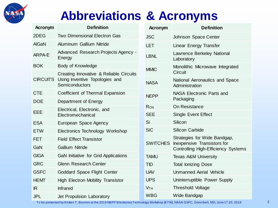
Abbreviations & Acronyms
2
Acronym Definition
2DEG Two Dimensional Electron Gas
AlGaN Aluminum Gallium Nitride
ARPA-E Advanced Research Projects Agency -Energy
BOK Body of Knowledge
CIRCUITSCreating Innovative & Reliable Circuits Using Inventive Topologies and Semiconductors
CTE Coefficient of Thermal Expansion
DOE Department of Energy
EEE Electrical, Electronic, and Electromechanical
ESA European Space Agency
ETW Electronics Technology Workshop
FET Field Effect Transistor
GaN Gallium Nitride
GIGA GaN Initiative for Grid Applications
GRC Glenn Research Center
GSFC Goddard Space Flight Center
HEMT High Electron Mobility Transistor
IR Infrared
JPL Jet Propulsion Laboratory
Acronym Definition
JSC Johnson Space Center
LET Linear Energy Transfer
LBNL Lawrence Berkeley National Laboratory
MMIC Monolithic Microwave Integrated Circuit
NASA National Aeronautics and Space Administration
NEPP NASA Electronic Parts and Packaging
RON On ResistanceSEE Single Event EffectSi SiliconSiC Silicon Carbide
SWITCHESStrategies for Wide Bandgap, Inexpensive Transistors for Controlling High-Efficiency Systems
TAMU Texas A&M UniversityTID Total Ionizing DoseUAV Unmanned Aerial VehicleUPS Uninterruptible Power SupplyVTH Threshold VoltageWBG Wide Bandgap
To be presented by Kristen T. Boomer at the 2019 NEPP Electronics Technology Workshop (ETW), NASA GSFC, Greenbelt, MD, June 17-20, 2019
Body of Knowledge Documents
• Provide a brief guidance to a technology and create a “snapshot” of the current status– Technology overview– NASA Applications– Other current work (government, industry, academia)– Challenges– Reliability– Future direction
• SiC BOK was completed in 2017 by members of NEPP Wide Bandgap (WBG) working group; GaNBOK to be released soon
3To be presented by Kristen T. Boomer at the 2019 NEPP Electronics Technology Workshop (ETW), NASA GSFC, Greenbelt, MD, June 17-20, 2019
Why WBG Devices?
• Majority of today’s electronics based on Si technology
• Approaching theoretical limit of Si technology• New operational environments• Stringent application requirements• Evolving technology: WBG semiconductors• SiC and GaN most promising candidates,
especially for power electronics
4To be presented by Kristen T. Boomer at the 2019 NEPP Electronics Technology Workshop (ETW), NASA GSFC, Greenbelt, MD, June 17-20, 2019
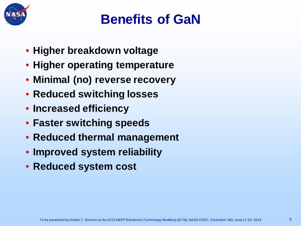
Benefits of GaN
• Higher breakdown voltage• Higher operating temperature• Minimal (no) reverse recovery• Reduced switching losses• Increased efficiency• Faster switching speeds• Reduced thermal management• Improved system reliability• Reduced system cost
5To be presented by Kristen T. Boomer at the 2019 NEPP Electronics Technology Workshop (ETW), NASA GSFC, Greenbelt, MD, June 17-20, 2019

Relative Comparison of Semiconductors
6To be presented by Kristen T. Boomer at the 2019 NEPP Electronics Technology Workshop (ETW), NASA GSFC, Greenbelt, MD, June 17-20, 2019
Property (relative to Si) Si SiC GaNThermal Conductivity 1 3.1 0.9Thermal Expansion Coefficient 1 1.6 2.2Dielectric Constant 1 0.9 0.9Electron Mobility 1 0.67 0.83Hole Mobility 1 0.08 0.42Breakdown Electric Field 1 7.34 6.67Saturation Velocity 1 2 2.2Maximum Working temperature 1 5.2 5.34
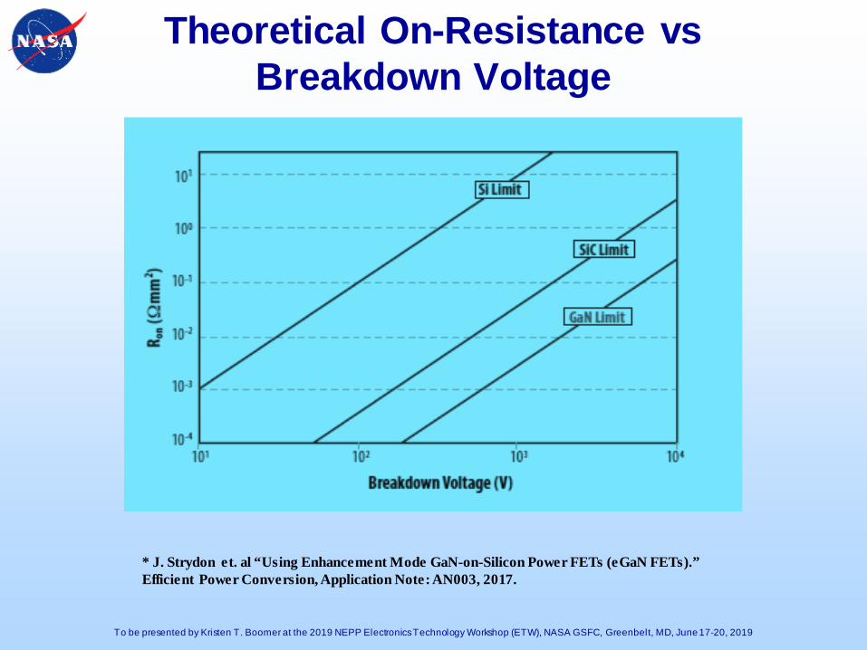
Theoretical On-Resistance vs Breakdown Voltage
To be presented by Kristen T. Boomer at the 2019 NEPP Electronics Technology Workshop (ETW), NASA GSFC, Greenbelt, MD, June 17-20, 2019
* J. Strydon et. al “Using Enhancement Mode GaN-on-Silicon Power FETs (eGaN FETs).”Efficient Power Conversion, Application Note: AN003, 2017.
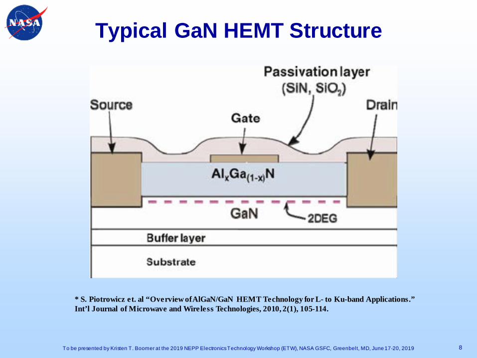
Typical GaN HEMT Structure
8To be presented by Kristen T. Boomer at the 2019 NEPP Electronics Technology Workshop (ETW), NASA GSFC, Greenbelt, MD, June 17-20, 2019
* S. Piotrowicz et. al “Overview of AlGaN/GaN HEMT Technology for L- to Ku-band Applications.” Int’l Journal of Microwave and Wireless Technologies, 2010, 2(1), 105-114.
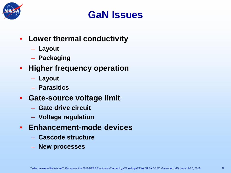
GaN Issues
• Lower thermal conductivity– Layout– Packaging
• Higher frequency operation– Layout– Parasitics
• Gate-source voltage limit– Gate drive circuit– Voltage regulation
• Enhancement-mode devices– Cascode structure– New processes
9To be presented by Kristen T. Boomer at the 2019 NEPP Electronics Technology Workshop (ETW), NASA GSFC, Greenbelt, MD, June 17-20, 2019
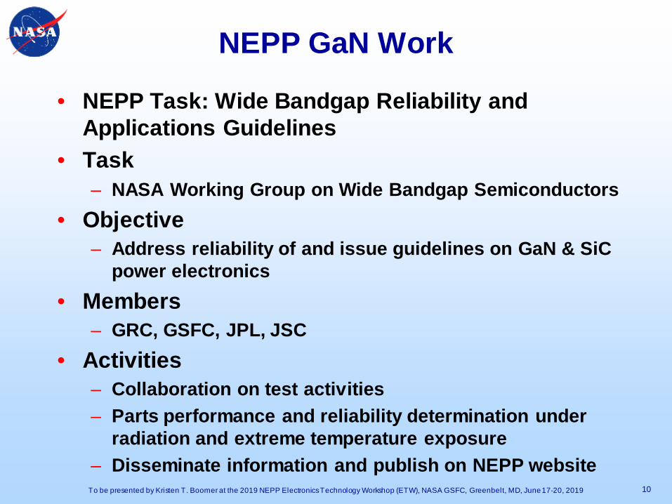
NEPP GaN Work
• NEPP Task: Wide Bandgap Reliability and Applications Guidelines
• Task– NASA Working Group on Wide Bandgap Semiconductors
• Objective– Address reliability of and issue guidelines on GaN & SiC
power electronics• Members
– GRC, GSFC, JPL, JSC• Activities
– Collaboration on test activities– Parts performance and reliability determination under
radiation and extreme temperature exposure– Disseminate information and publish on NEPP website
10To be presented by Kristen T. Boomer at the 2019 NEPP Electronics Technology Workshop (ETW), NASA GSFC, Greenbelt, MD, June 17-20, 2019
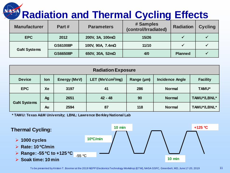
Radiation and Thermal Cycling Effects
11To be presented by Kristen T. Boomer at the 2019 NEPP Electronics Technology Workshop (ETW), NASA GSFC, Greenbelt, MD, June 17-20, 2019
Manufacturer Part # Parameters # Samples(control/Irradiated) Radiation Cycling
EPC 2012 200V, 3A, 100mΩ 15/26
GaN SystemsGS61008P 100V, 90A, 7.4mΩ 11/10
GS66508P 650V, 30A, 52mΩ 4/0 Planned
Radiation Exposure
Device Ion Energy (MeV) LET (MeV.cm2/mg) Range (μm) Incidence Angle Facility
EPC Xe 3197 41 286 Normal TAMU*
GaN SystemsAg 2651 42 - 48 90 Normal TAMU*/LBNL*
Au 2594 87 118 Normal TAMU*/LBNL*
10ºC/min
10 min
10 min
+125 ºC
-55 ºC
Thermal Cycling:
1000 cycles Rate: 10 ºC/min Range: -55 ºC to +125 ºC Soak time: 10 min
* TAMU: Texas A&M University; LBNL: Lawrence Berkley National Lab
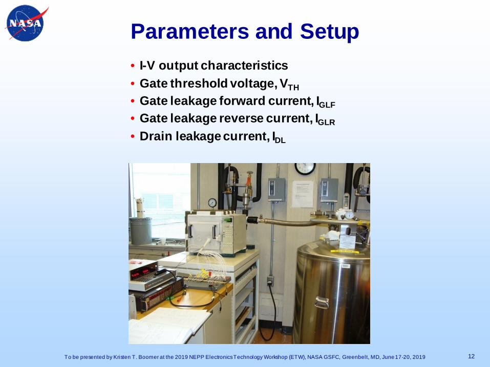
Parameters and Setup
12
• I-V output characteristics• Gate threshold voltage, VTH
• Gate leakage forward current, IGLF
• Gate leakage reverse current, IGLR
• Drain leakage current, IDL
To be presented by Kristen T. Boomer at the 2019 NEPP Electronics Technology Workshop (ETW), NASA GSFC, Greenbelt, MD, June 17-20, 2019
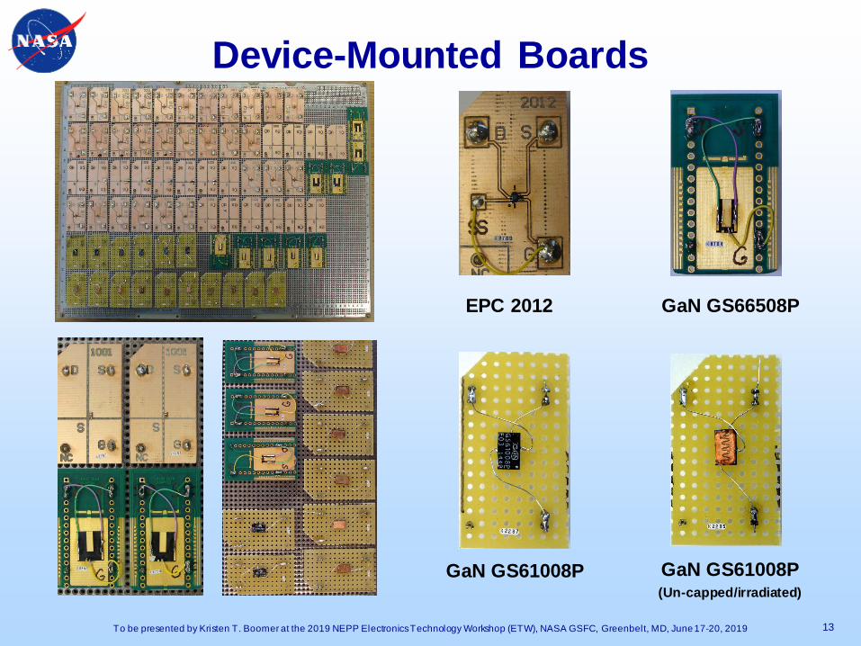
Device-Mounted Boards
13
EPC 2012
GaN GS61008P
GaN GS66508P
GaN GS61008P(Un-capped/irradiated)
To be presented by Kristen T. Boomer at the 2019 NEPP Electronics Technology Workshop (ETW), NASA GSFC, Greenbelt, MD, June 17-20, 2019
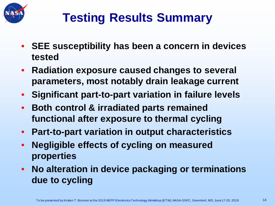
Testing Results Summary
• SEE susceptibility has been a concern in devices tested
• Radiation exposure caused changes to several parameters, most notably drain leakage current
• Significant part-to-part variation in failure levels• Both control & irradiated parts remained
functional after exposure to thermal cycling• Part-to-part variation in output characteristics• Negligible effects of cycling on measured
properties• No alteration in device packaging or terminations
due to cycling
14To be presented by Kristen T. Boomer at the 2019 NEPP Electronics Technology Workshop (ETW), NASA GSFC, Greenbelt, MD, June 17-20, 2019
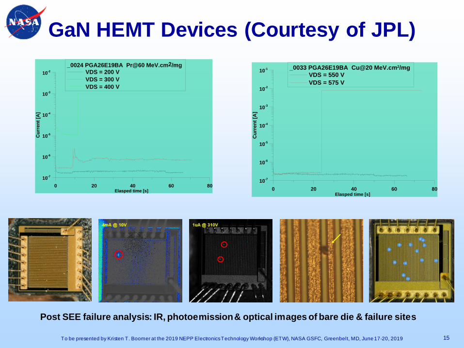
GaN HEMT Devices (Courtesy of JPL)
15
0 20 40 60 80Elasped time [s]
10-7
10-6
10-5
10-4
10-3
10-2
Cur
rent
[A]
_0024 PGA26E19BA Pr@60 MeV.cm2/mg VDS = 200 VVDS = 300 VVDS = 400 V
0 20 40 60 80Elasped time [s]
10-7
10-6
10-5
10-4
10-3
10-2
10-1
Cur
rent
[A]
_0033 PGA26E19BA Cu@20 MeV.cm2/mg VDS = 550 VVDS = 575 V
Post SEE failure analysis: IR, photoemission & optical images of bare die & failure sites
To be presented by Kristen T. Boomer at the 2019 NEPP Electronics Technology Workshop (ETW), NASA GSFC, Greenbelt, MD, June 17-20, 2019
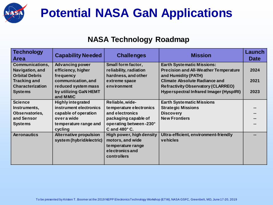
Potential NASA GaN Applications
To be presented by Kristen T. Boomer at the 2019 NEPP Electronics Technology Workshop (ETW), NASA GSFC, Greenbelt, MD, June 17-20, 2019
Technology Area Capability Needed Challenges Mission Launch
DateCommunications, Navigation, and Orbital Debris Tracking and Characterization Systems
Advancing power efficiency, higher frequency communication, and reduced system mass by utilizing GaN HEMT and MMIC
Small form factor, reliability, radiation hardness, and other extreme space environment
Earth Systematic Missions:Precision and All-Weather Temperature and Humidity (PATH)Climate Absolute Radiance and Refractivity Observatory (CLARREO)Hyperspectral Infrared Imager (HyspIRI)
2024
2021
2023
Science Instruments, Observatories, and Sensor Systems
Highly integrated instrument electronics capable of operation over a wide temperature range and cycling
Reliable, wide-temperature electronics and electronics packaging capable of operating between -230°C and 480° C.
Earth Systematic MissionsStrategic MissionsDiscoveryNew Frontiers
--------
Aeronautics Alternative propulsion system (hybrid/electric)
High power, high density motors, and wide temperature range electronics and controllers
Ultra-efficient, environment-friendly vehicles
--
NASA Technology Roadmap
Commercial Applications
17
• Motor drives• Uninterruptible power supplies (UPS)• Photovoltaic inverters• Power utilities, energy conversion, power
distribution• Automotive industry (hybrid/electric vehicle)• Industrial equipment• Consumer electronics, data & communication
networks• Down-hole drilling• Cellular base stations
To be presented by Kristen T. Boomer at the 2019 NEPP Electronics Technology Workshop (ETW), NASA GSFC, Greenbelt, MD, June 17-20, 2019
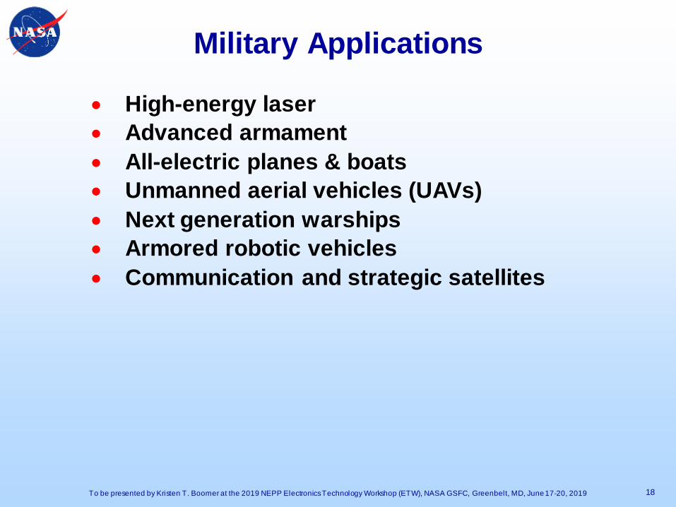
Military Applications
18
• High-energy laser• Advanced armament• All-electric planes & boats• Unmanned aerial vehicles (UAVs)• Next generation warships• Armored robotic vehicles• Communication and strategic satellites
To be presented by Kristen T. Boomer at the 2019 NEPP Electronics Technology Workshop (ETW), NASA GSFC, Greenbelt, MD, June 17-20, 2019
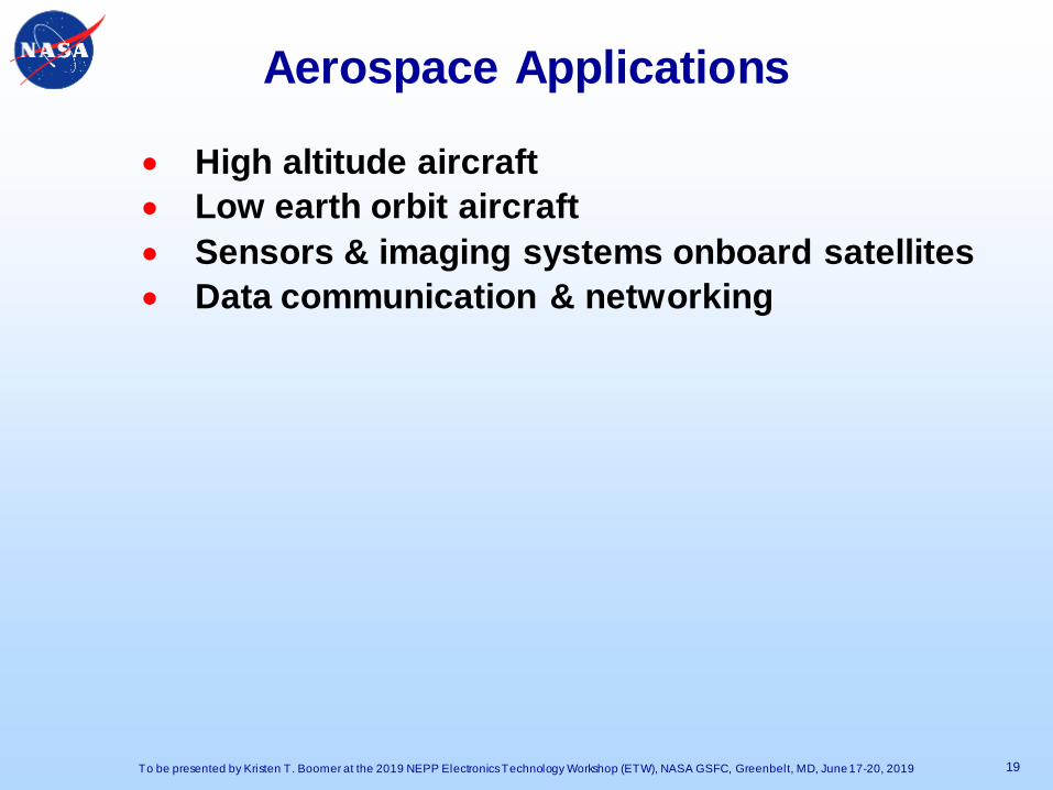
Aerospace Applications
19
• High altitude aircraft• Low earth orbit aircraft• Sensors & imaging systems onboard satellites• Data communication & networking
To be presented by Kristen T. Boomer at the 2019 NEPP Electronics Technology Workshop (ETW), NASA GSFC, Greenbelt, MD, June 17-20, 2019
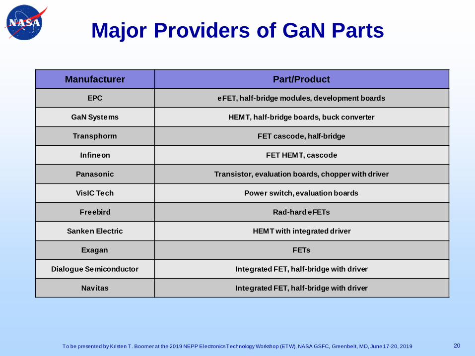
Major Providers of GaN Parts
20To be presented by Kristen T. Boomer at the 2019 NEPP Electronics Technology Workshop (ETW), NASA GSFC, Greenbelt, MD, June 17-20, 2019
Manufacturer Part/Product
EPC eFET, half-bridge modules, development boards
GaN Systems HEMT, half-bridge boards, buck converter
Transphorm FET cascode, half-bridge
Infineon FET HEMT, cascode
Panasonic Transistor, evaluation boards, chopper with driver
VisIC Tech Power switch, evaluation boards
Freebird Rad-hard eFETs
Sanken Electric HEMT with integrated driver
Exagan FETs
Dialogue Semiconductor Integrated FET, half-bridge with driver
Navitas Integrated FET, half-bridge with driver
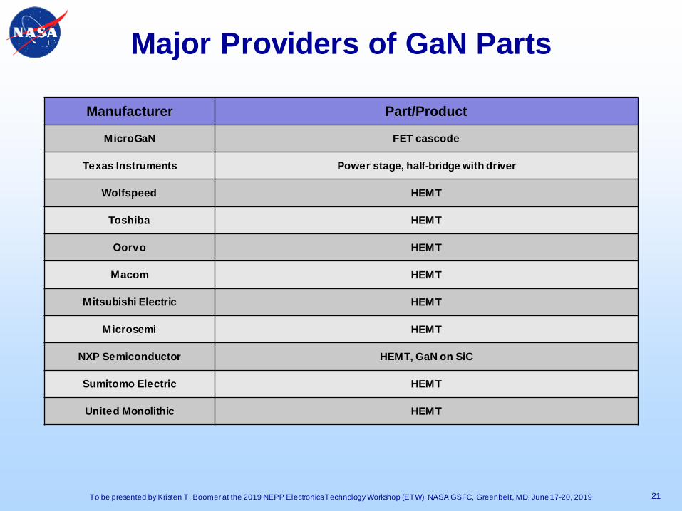
Major Providers of GaN Parts
21To be presented by Kristen T. Boomer at the 2019 NEPP Electronics Technology Workshop (ETW), NASA GSFC, Greenbelt, MD, June 17-20, 2019
Manufacturer Part/Product
MicroGaN FET cascode
Texas Instruments Power stage, half-bridge with driver
Wolfspeed HEMT
Toshiba HEMT
Oorvo HEMT
Macom HEMT
Mitsubishi Electric HEMT
Microsemi HEMT
NXP Semiconductor HEMT, GaN on SiC
Sumitomo Electric HEMT
United Monolithic HEMT
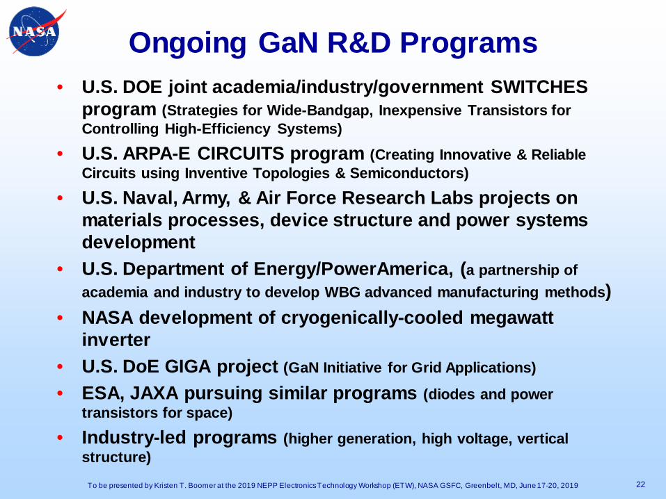
Ongoing GaN R&D Programs
22
• U.S. DOE joint academia/industry/government SWITCHES program (Strategies for Wide-Bandgap, Inexpensive Transistors for Controlling High-Efficiency Systems)
• U.S. ARPA-E CIRCUITS program (Creating Innovative & Reliable Circuits using Inventive Topologies & Semiconductors)
• U.S. Naval, Army, & Air Force Research Labs projects on materials processes, device structure and power systems development
• U.S. Department of Energy/PowerAmerica, (a partnership of academia and industry to develop WBG advanced manufacturing methods)
• NASA development of cryogenically-cooled megawatt inverter
• U.S. DoE GIGA project (GaN Initiative for Grid Applications)
• ESA, JAXA pursuing similar programs (diodes and power transistors for space)
• Industry-led programs (higher generation, high voltage, vertical structure)
To be presented by Kristen T. Boomer at the 2019 NEPP Electronics Technology Workshop (ETW), NASA GSFC, Greenbelt, MD, June 17-20, 2019
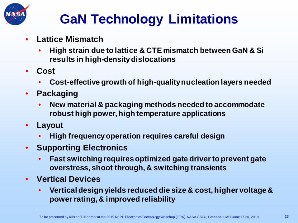
GaN Technology Limitations
23
• Lattice Mismatch• High strain due to lattice & CTE mismatch between GaN & Si
results in high-density dislocations• Cost
• Cost-effective growth of high-quality nucleation layers needed• Packaging
• New material & packaging methods needed to accommodate robust high power, high temperature applications
• Layout• High frequency operation requires careful design
• Supporting Electronics• Fast switching requires optimized gate driver to prevent gate
overstress, shoot through, & switching transients• Vertical Devices
• Vertical design yields reduced die size & cost, higher voltage & power rating, & improved reliability
To be presented by Kristen T. Boomer at the 2019 NEPP Electronics Technology Workshop (ETW), NASA GSFC, Greenbelt, MD, June 17-20, 2019
Acknowledgements• This work was performed in support of the NASA
Electronic Parts and Packaging (NEPP) Program. Part of this effort was performed at the NASA Glenn Research Center under GESS-3 Contract Number NNC12BA01B.
24To be presented by Kristen T. Boomer at the 2019 NEPP Electronics Technology Workshop (ETW), NASA GSFC, Greenbelt, MD, June 17-20, 2019