Embed Size (px)
Citation preview

241-208 CH6 1
Chapter 6
Functions of Combinational Logic
By Taweesak Reungpeerakul

241-208 CH6 2
Contents Adders Comparators Decoders Encoders Code Converters Multiplexers Demultiplexers Parity Generators

241-208 CH6 3
6.1 Basic Adders
Full AdderA B Cin SUM Cout0 0 0 0 00 0 1 1 00 1 0 1 00 1 1 0 11 0 0 1 01 0 1 0 11 1 0 0 11 1 1 1 1
Half AdderA B SUM Cout
0 0 0 00 1 1 01 0 1 01 1 0 1
SUM = AB
Cout = AB
SUM = ABCin
Cout = AB+(AB)Cin

241-208 CH6 4
Logic Symbol and Diagram
Half Adder Full Adder
B
A
∑
Cout
∑B
A
∑
Cout
∑
Cin
Cout
A
SUMB
Cin
A
SUM
B
Cout
241-208 CH6 5
Full Adder by 2 Half Adders
Half Adder Full Adder
B
A
∑
Cout
∑
A
SUM
B
Cout
SUM = ABCin
Cout = AB+(AB)Cin
B
A
∑
Cout
∑SUM
Cout
B
A
∑
Cout
∑A
B
Cin
AB
AB
241-208 CH6 6
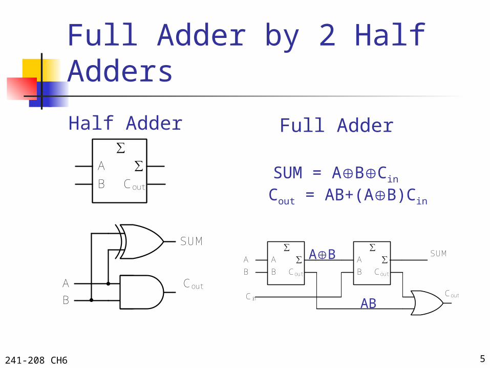
6.2 Parallel Binary Adder
A1 B1
BA
Cout ∑
BA
Cout ∑
Cin
A2 B2
S2 S1S3
A2A1
+B2B1
S3S2S1
A1 B1
BA
Cout ∑
Cin
A2 B2
S2 S1S3
BA
Cout ∑
Cin
A full adder is required for each
bit in the numbers.
Question: 4-bit numbers

241-208 CH6 7
Four Adders
A1 B1
BA
Cout ∑
Cin
A2 B2
S2 S1
C2
BA
Cout ∑
Cin
A3 B3
BA
Cout ∑
Cin
A4 B4
S4 S3C4
BA
Cout ∑
Cin
C1C3
A B Cn-1 Sn
Cn0 0 0 0
00 0 1 1
00 1 0 1
00 1 1 0
11 0 0 1
01 0 1 0
11 1 0 0
11 1 1 1
1

241-208 CH6 8
IC:4-bit Parallel Adder
Example: 74LS83A (or 74LS283)
74LS83A74LS283
Question: Show circuit diagram of A+B by using 74LS83A. A = 00001111 and B = 01011100

241-208 CH6 9
6.3 Comparators
Equality Comparing A and B: AB
If A=B, output = 0 If A≠B, output = 1
HIGH indicates equality: AB (XNOR)
A1A0 ? B1B0
A1
1 if A=BB1
A0
B0
0 if A¹B
Inequality IC: 74LS85
Question: Show circuit diagram in order to compare two 8-bit numbers by using 74LS85.
A1
A0
A2
A3
B1
B0
B2
B3
Cascading inputs
COMP
A = B
A < B
A > BA = B
A < B
A > B
0
0
3
3
A
B
Outputs

241-208 CH6 10
Two 74LS85 Cascaded Arrangement
Outputs
A1
A0
A2
A3
B1
B0
B2
B3
COMP
A = B
A < B
A > BA = B
A < B
A > B
0
0
3
3
A
A
A5
A4
A6
A7
B5
B4
B6
B7
+5.0 V
COMP
A = B
A < B
A > BA = B
A < B
A > B
0
0
3
3
A
A
LSBs MSBs

241-208 CH6 11
6.4 Decoders
A decoder is a logic circuit that detects the presence of a specific combination of bits at its input.
A1
A0
A2
A3
OUT A1
A0
A2
A3
OUT
Active HIGH decoder for 0011 Active LOW decoder for 0011

241-208 CH6 12
4-to-16 Decoder
Bin/Dec
A0
0123456789
101112131415
4-bit binaryinput
Decimaloutputs
A1
A2
A3
1
1
0
1111111111101111
1
15
1213
14
1
23
4
910
11
56
7
8
0
&
48
1
2
IC: 74HC154
A0A1A2
A3
CS1
CS2
Question: Use 74HC154 to implement the logic in order to support a 5-bit number.

241-208 CH6 13
BCD-to-Decimal Decoder BCD-to-decimal decoders accept a binary coded decimal
input and activate one of ten possible decimal digit indications.
IC: 74HC42BCD/DEC
012
3456789
12
48
74HC42
(11)(10)(9)(7)(6)(5)(4)(3)(2)
(1)
(15)(14)(13)(12)
A1
A0
A2
A3
Question: Assume the inputs to the 74HC42 decoder are the sequence 0101, 0110, 0011, and 0010. Describe the output.
Answer: All lines are HIGH except for one active output, which is LOW. The active outputs are 5, 6, 3, and 2 in that order.
Question: Write truth table of output 0.

241-208 CH6 14
BCD-to-7-Segment Decoder
IC: 74LS47 BCD Inputs (D-A) 7-segment Outputs (a
-g) Ripple Blanking Input
(RBI) Blanking Input/Ripple
Blanking Output (BI/RBO)
Lamp Test (LT) Zero Suppression
a
b
c
d
e
f
g
1
2
4
8
(16)
(4)
(13)
(12)
(11)
(10)
(9)
(15)
(14)
(1)
(2)
(6)
(7)
(3)
(5)
(8)
BCD inputs
Outputs to seven segment device
GND
VCC
BCD/7-seg
BI/RBO BI/RBO
LT
RBI
LT
RBI
74LS47

241-208 CH6 15
Illustration of Leading Zero Suppression
abcdefg BI/RBO
0 0 0 0
8 4 2 1RBI LT
0
74LS47
abcdefg BI/RBO
0 0 0 0
8 4 2 1RBI LT
0
74LS47
abcdefg BI/RBO
0 0 1 1
8 4 2 1RBI LT
0
74LS47
abcdefg BI/RBO
0 0 0 0
8 4 2 1RBI LT
1
74LS47

241-208 CH6 16
Illustration of Trailing Zero Suppression
abcdefg BI/RBO
0 1 0 1
8 4 2 1RBI LT
74LS47
1
abcdefg BI/RBO
0 1 1 1
8 4 2 1RBI LT
74LS47
abcdefg BI/RBO
0 0 0 0
8 4 2 1RBI LT
74LS47
0
abcdefg BI/RBO
0 0 0 0
8 4 2 1RBI LT
74LS47
0
241-208 CH6 17
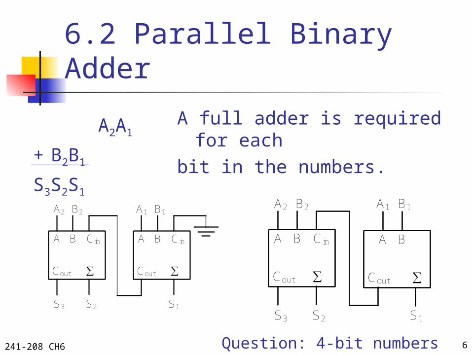
6.5 Encoders
An encoder accepts an active logic level on one of its inputs representing a digit, such as a decimal or octal digits, and converts it to a coded output, such as BCD or binary.
IC: 74HC147 16-to-4 encoder (decimal-to-BCD)
IC: 74F148 8-to-3 encoder
A1
A0
A2
A3
1
2
3
45678
9

241-208 CH6 18
Example Show how the decimal-to-BCD encoder
converts the decimal number 3 into a BCD 0011.
A1
A0
A2
A3
1
2
3
45678
9
0
0
0
00
0
0
0
1
0
0
1
1

241-208 CH6 19
74HC147
The 74HC147 is an example of an IC encoder. It has ten active-LOW inputs and converts the active input to an active-LOW BCD output.
This device offers additional flexibility with a priority encoder.
Decimal input
BCD output
1
2
4
8
(16)
(11)
(12)
(13)
(1)
(2)
(4)
(3)
(5)
(9)
(7)
(6)
(14)
(8)
1
2
3
4
5
6
7
8(10) 9
GND
VCC
HPRI/BCD
74HC147
Means highest value input has priority

241-208 CH6 20
A Simplified Keyboard Encoder
123456789
1248
987
65
321
0
4
R7 R8 R9
R4 R5 R6
R1 R2 R3
R0
BCD complement of key press
Not used by this encoder but may be used by other circuits to detect the key press.
VCC

241-208 CH6 21
6.6 Code Converters BCD-to-BIN Conversion IC: 74184
BIN-to-BCD Conversion IC: 74185

241-208 CH6 22
Code Converters (cont.) BIN-to-Gray Gray-to-BIN
MSB
LSB
MSB
LSB
B0 G0
B3
B2
B1
B0
G3
G2
G1
G0
G3
G2
G1
B3
B2
B1
Question: Show the conversion of binary 0111 to Gray and vice versa.

241-208 CH6 23
6.7 Multiplexers (MUX)
A multiplexer has several data-input lines and a single output line.
It also has data-select inputs, which permit digital data on any one of the inputs to be switched to the output line.
Another name is a data selector.
IC: 74HC157 Quad 2-input MUX
IC: 74HC151 8-input MUX
MUX
1
2
0
3
1
0Data select
Data inputs
Data outputD1
D0
D2
D3
S1
S010
Question: Which data line is selected if S1S0 = 10?

241-208 CH6 24
ICs 74HC157 Quad 2-input
MUX
74HC151 8-input MUX
241-208 CH6 25
Y1
Y2
Y3
Y4
Y5
Y6
Y7
Y0
DEMUX
AAA
0
1
2
GGG
1
2A
2B
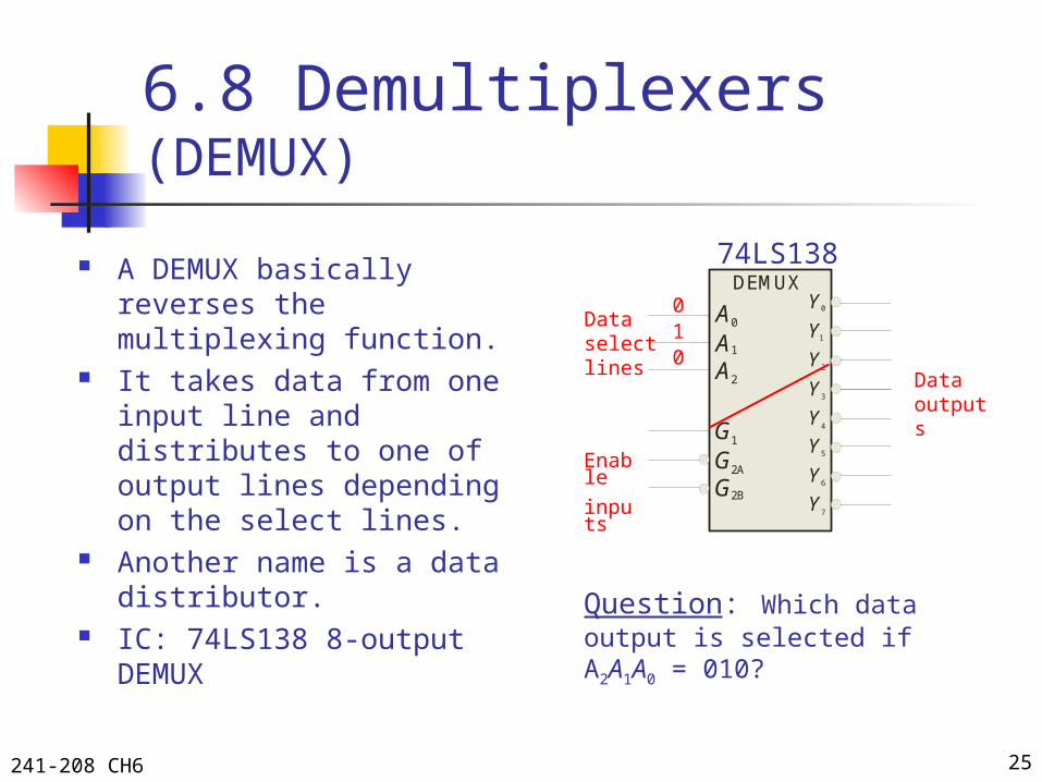
6.8 Demultiplexers (DEMUX)
A DEMUX basically reverses the multiplexing function.
It takes data from one input line and distributes to one of output lines depending on the select lines.
Another name is a data distributor.
IC: 74LS138 8-output DEMUX
10
Question: Which data output is selected if A2A1A0 = 010?
74LS138
Data select lines
Enable
inputs
Data outputs
0

241-208 CH6 26
Example (DEMUX)
Determine the outputs, given the inputs shown.
A0
Y0
Y1
Y2
Y3
Y4
Y5
Y6
Y7
A1
A2
G1
G2A
G2B
LOW
LOW
74LS138
Y1
Y2
Y3
Y4
Y5
Y6
Y7
Y0
DEMUX
AAA
0
1
2
GGG
1
2A
2B
Data select lines
Enable
inputs
Data outputs

241-208 CH6 27
6.9 Parity Generators/Checkers
One method of error detections is to use parity.
A parity bit is attached to a group of data in order to make the total number of 1s either even or odd.
11010011data with odd parity =data with even parity = 01010011
The data is 1010011. Show the parity bit for the data with odd and even parity.

241-208 CH6 28
6.9 Parity Generators/Checkers (cont.)
IC: 74LS280 9-bit parity generator/checker
(8 bits+1 parity bit)
Checker:# of 1s on inputs ∑ Even ∑ Odd0,2,4,6,8 H L1,3,5,7,9 L H
Generator: To generate even parity, the parity bit is taken from the odd parity output. To generate odd parity, the output is taken from the even parity output.
(5)(6)
(13)
(1)
(11)
(12)
(2)
(10)
(9)
(8)
F
G
D
E
H
C
B
A
(4)I
74LS280
Data inputs
Even Odd


![WATERQUALITYSTANDARDS · IAC10/7/20 EnvironmentalProtection[567] Ch61,p.5 3. Thedistancetotheupstreamlimitsofanestablishedrecreationalarea,suchaspublicbeaches, andstate,county,andlocalparks](https://img.pdfslide.net/doc/110x75/6120c1ed3da6874dd54e814a/waterqualitystandards-iac10720-environmentalprotection567-ch61p5-3-thedistancetotheupstreamlimitsofanestablishedrecreationalareasuchaspublicbeaches.jpg)