Embed Size (px)
Citation preview
2003 Microchip Technology Inc. Preliminary DS21822C-page 1
25AA256/25LC256
Device Selection Table
Features
• Max. clock 10 MHz
• Low-power CMOS technology- Max. Write Current: 5 mA at 5.5V, 10 MHz
- Read Current: 5 mA at 5.5V, 10 MHz- Standby Current: 1 µA at 5.5V
• 32,768 x 8-bit organization
• 64 byte page• Self-timed ERASE and WRITE cycles (5 ms
max.)• Block write protection
- Protect none, 1/4, 1/2 or all of array
• Built-in write protection- Power-on/off data protection circuitry- Write enable latch
- Write-protect pin• Sequential read• High reliability
- Endurance: 1,000,000 erase/write cycles- Data retention: > 200 years- ESD protection: > 4000V
• Temperature ranges supported;
• Standard and Pb-free packages available
Pin Function Table
Description
The Microchip Technology Inc. 25AA256/25LC256(25XX256*) are 256k-bit Serial Electrically ErasablePROMs. The memory is accessed via a simple SerialPeripheral Interface™ (SPI™) compatible serial bus.The bus signals required are a clock input (SCK) plusseparate data in (SI) and data out (SO) lines. Access tothe device is controlled through a Chip Select (CS)input.
Communication to the device can be paused via thehold pin (HOLD). While the device is paused,transitions on its inputs will be ignored, with theexception of Chip Select, allowing the host to servicehigher priority interrupts.
The 25XX256 is available in standard packagesincluding 8-lead PDIP and SOIC, and advancedpackaging including 8-lead DFN and 8-lead TSSOP.Pb-free (Pure Sn) finish is also available.
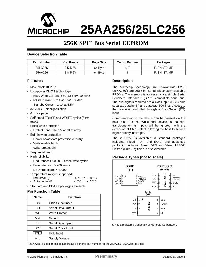
Package Types (not to scale)
Part Number VCC Range Page Size Temp. Ranges Packages
25LC256 2.5-5.5V 64 Byte I, E P, SN, ST, MF
25AA256 1.8-5.5V 64 Byte I P, SN, ST, MF
- Industrial (I): -40°C to +85°C- Automotive (E): -40°C to +125°C
Name Function
CS Chip Select Input
SO Serial Data Output
WP Write-Protect
VSS Ground
SI Serial Data Input
SCK Serial Clock Input
HOLD Hold Input
VCC Supply Voltage
25LC
256
CS
SO
WP
VSS
12
3
4
87
6
5
VCC
HOLD
SCK
SI
PDIP/SOIC(P, SN)
TSSOP
CSSOWPVSS
1234
8765
VCCHOLDSCKSI
(ST)
DFN
CS
SO
WP
VSS
HOLD
SCK
SI
25LC
256
5
6
7
8
4
3
2
1 VCC
(MF)
256K SPI™ Bus Serial EEPROM
SPI is a registered trademark of Motorola Corporation.
* 25XX256 is used in this document as a generic part number for the 25AA256, 25LC256 devices.
25AA256/25LC256
DS21822C-page 2 Preliminary 2003 Microchip Technology Inc.
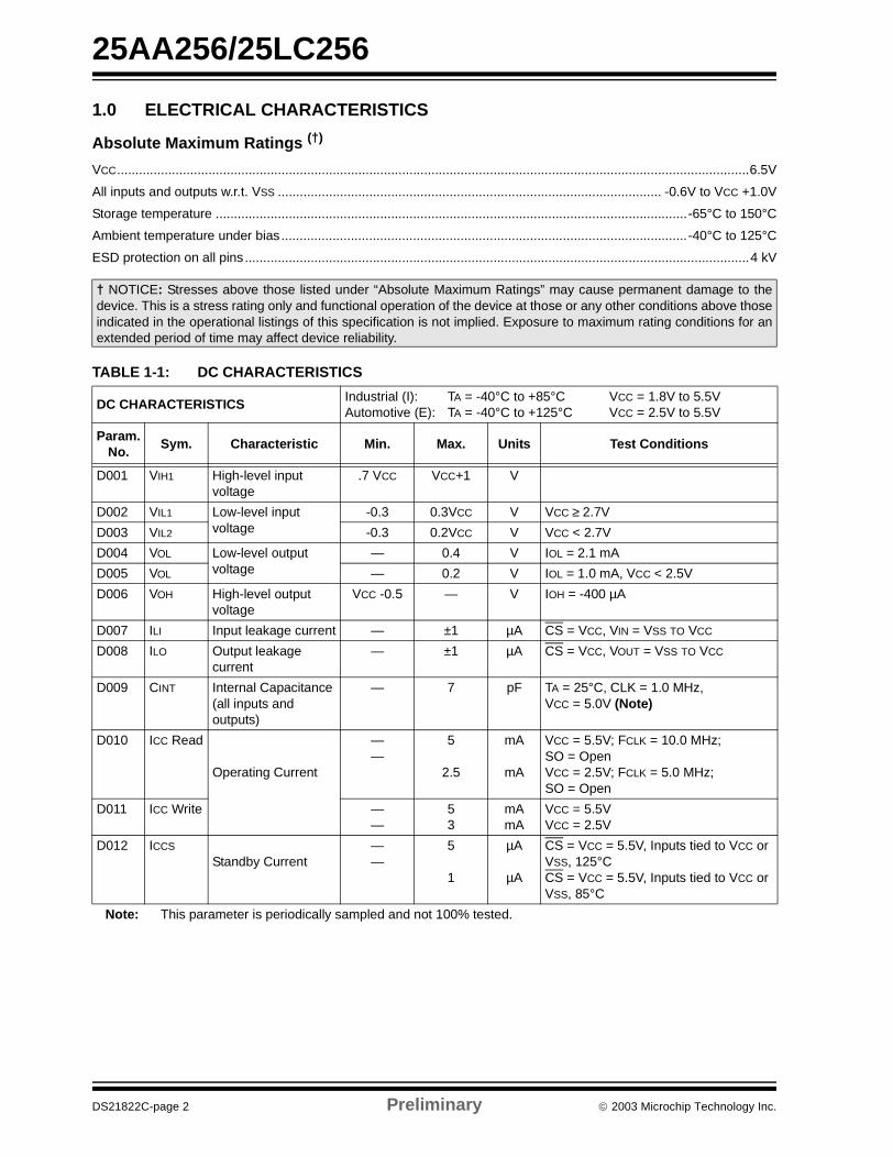
1.0 ELECTRICAL CHARACTERISTICS
Absolute Maximum Ratings (†)
VCC.............................................................................................................................................................................6.5V
All inputs and outputs w.r.t. VSS ......................................................................................................... -0.6V to VCC +1.0V
Storage temperature .................................................................................................................................-65°C to 150°C
Ambient temperature under bias ...............................................................................................................-40°C to 125°C
ESD protection on all pins ..........................................................................................................................................4 kV
TABLE 1-1: DC CHARACTERISTICS
† NOTICE: Stresses above those listed under “Absolute Maximum Ratings” may cause permanent damage to thedevice. This is a stress rating only and functional operation of the device at those or any other conditions above thoseindicated in the operational listings of this specification is not implied. Exposure to maximum rating conditions for anextended period of time may affect device reliability.
DC CHARACTERISTICSIndustrial (I): TA = -40°C to +85°C VCC = 1.8V to 5.5VAutomotive (E): TA = -40°C to +125°C VCC = 2.5V to 5.5V
Param.No.
Sym. Characteristic Min. Max. Units Test Conditions
D001 VIH1 High-level input voltage
.7 VCC VCC+1 V
D002 VIL1 Low-level inputvoltage
-0.3 0.3VCC V VCC ≥ 2.7V
D003 VIL2 -0.3 0.2VCC V VCC < 2.7V
D004 VOL Low-level outputvoltage
— 0.4 V IOL = 2.1 mA
D005 VOL — 0.2 V IOL = 1.0 mA, VCC < 2.5V
D006 VOH High-level outputvoltage
VCC -0.5 — V IOH = -400 µA
D007 ILI Input leakage current — ±1 µA CS = VCC, VIN = VSS TO VCC
D008 ILO Output leakage current
— ±1 µA CS = VCC, VOUT = VSS TO VCC
D009 CINT Internal Capacitance(all inputs and outputs)
— 7 pF TA = 25°C, CLK = 1.0 MHz,VCC = 5.0V (Note)
D010 ICC Read
Operating Current
——
5
2.5
mA
mA
VCC = 5.5V; FCLK = 10.0 MHz; SO = OpenVCC = 2.5V; FCLK = 5.0 MHz; SO = Open
D011 ICC Write ——
53
mAmA
VCC = 5.5VVCC = 2.5V
D012 ICCS
Standby Current——
5
1
µA
µA
CS = VCC = 5.5V, Inputs tied to VCC or VSS, 125°CCS = VCC = 5.5V, Inputs tied to VCC or VSS, 85°C
Note: This parameter is periodically sampled and not 100% tested.
2003 Microchip Technology Inc. Preliminary DS21822C-page 3
25AA256/25LC256
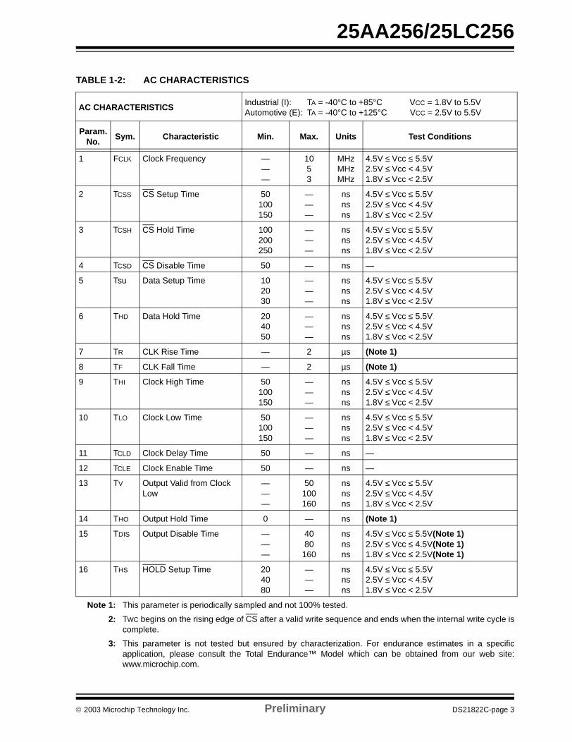
TABLE 1-2: AC CHARACTERISTICS
AC CHARACTERISTICSIndustrial (I): TA = -40°C to +85°C VCC = 1.8V to 5.5VAutomotive (E): TA = -40°C to +125°C VCC = 2.5V to 5.5V
Param.No.
Sym. Characteristic Min. Max. Units Test Conditions
1 FCLK Clock Frequency ———
1053
MHzMHzMHz
4.5V ≤ Vcc ≤ 5.5V2.5V ≤ Vcc < 4.5V1.8V ≤ Vcc < 2.5V
2 TCSS CS Setup Time 50100150
———
nsnsns
4.5V ≤ Vcc ≤ 5.5V2.5V ≤ Vcc < 4.5V1.8V ≤ Vcc < 2.5V
3 TCSH CS Hold Time 100200250
———
nsnsns
4.5V ≤ Vcc ≤ 5.5V2.5V ≤ Vcc < 4.5V1.8V ≤ Vcc < 2.5V
4 TCSD CS Disable Time 50 — ns —
5 Tsu Data Setup Time 102030
———
nsnsns
4.5V ≤ Vcc ≤ 5.5V2.5V ≤ Vcc < 4.5V1.8V ≤ Vcc < 2.5V
6 THD Data Hold Time 204050
———
nsnsns
4.5V ≤ Vcc ≤ 5.5V2.5V ≤ Vcc < 4.5V1.8V ≤ Vcc < 2.5V
7 TR CLK Rise Time — 2 µs (Note 1)
8 TF CLK Fall Time — 2 µs (Note 1)
9 THI Clock High Time 50100150
———
nsnsns
4.5V ≤ Vcc ≤ 5.5V2.5V ≤ Vcc < 4.5V1.8V ≤ Vcc < 2.5V
10 TLO Clock Low Time 50100150
———
nsnsns
4.5V ≤ Vcc ≤ 5.5V2.5V ≤ Vcc < 4.5V1.8V ≤ Vcc < 2.5V
11 TCLD Clock Delay Time 50 — ns —
12 TCLE Clock Enable Time 50 — ns —
13 TV Output Valid from Clock Low
———
50100160
nsnsns
4.5V ≤ Vcc ≤ 5.5V2.5V ≤ Vcc < 4.5V1.8V ≤ Vcc < 2.5V
14 THO Output Hold Time 0 — ns (Note 1)
15 TDIS Output Disable Time ———
4080
160
nsnsns
4.5V ≤ Vcc ≤ 5.5V(Note 1)2.5V ≤ Vcc ≤ 4.5V(Note 1)1.8V ≤ Vcc ≤ 2.5V(Note 1)
16 THS HOLD Setup Time 204080
———
nsnsns
4.5V ≤ Vcc ≤ 5.5V2.5V ≤ Vcc < 4.5V1.8V ≤ Vcc < 2.5V
Note 1: This parameter is periodically sampled and not 100% tested.
2: TWC begins on the rising edge of CS after a valid write sequence and ends when the internal write cycle iscomplete.
3: This parameter is not tested but ensured by characterization. For endurance estimates in a specificapplication, please consult the Total Endurance™ Model which can be obtained from our web site:www.microchip.com.
25AA256/25LC256
DS21822C-page 4 Preliminary 2003 Microchip Technology Inc.
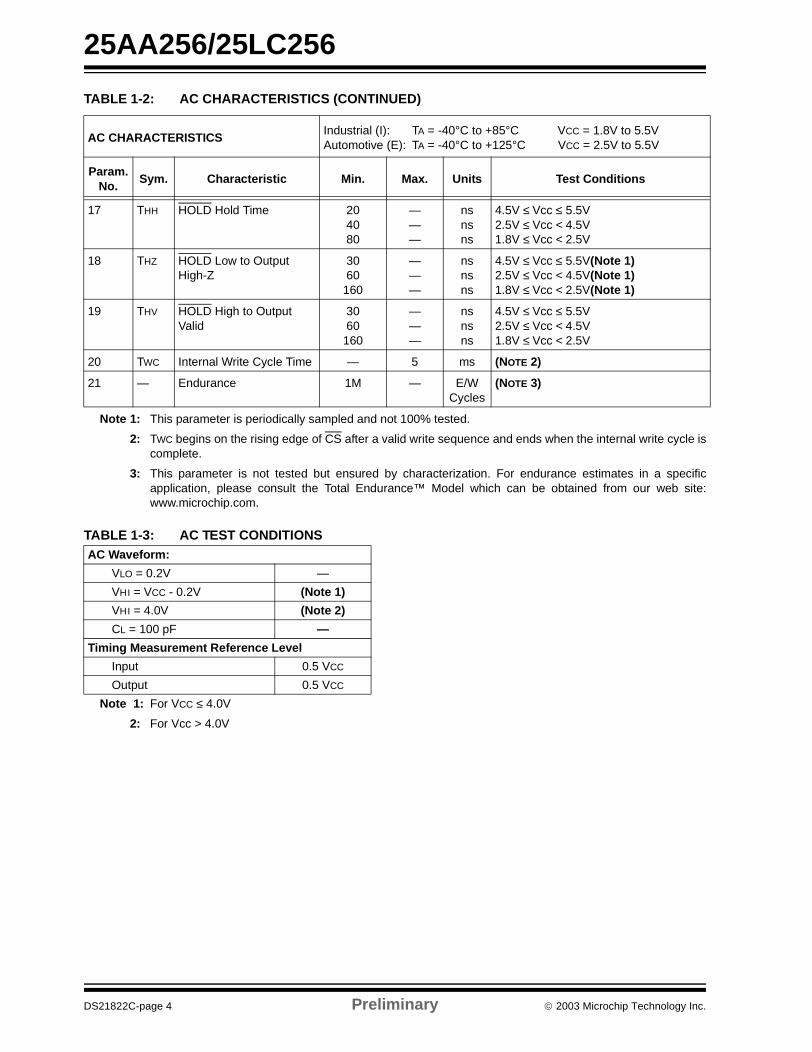
TABLE 1-3: AC TEST CONDITIONS
17 THH HOLD Hold Time 204080
———
nsnsns
4.5V ≤ Vcc ≤ 5.5V2.5V ≤ Vcc < 4.5V1.8V ≤ Vcc < 2.5V
18 THZ HOLD Low to Output High-Z
3060
160
———
nsnsns
4.5V ≤ Vcc ≤ 5.5V(Note 1)2.5V ≤ Vcc < 4.5V(Note 1)1.8V ≤ Vcc < 2.5V(Note 1)
19 THV HOLD High to Output Valid
3060
160
———
nsnsns
4.5V ≤ Vcc ≤ 5.5V2.5V ≤ Vcc < 4.5V1.8V ≤ Vcc < 2.5V
20 TWC Internal Write Cycle Time — 5 ms (NOTE 2)
21 — Endurance 1M — E/W Cycles
(NOTE 3)
TABLE 1-2: AC CHARACTERISTICS (CONTINUED)
AC CHARACTERISTICSIndustrial (I): TA = -40°C to +85°C VCC = 1.8V to 5.5VAutomotive (E): TA = -40°C to +125°C VCC = 2.5V to 5.5V
Param.No.
Sym. Characteristic Min. Max. Units Test Conditions
Note 1: This parameter is periodically sampled and not 100% tested.
2: TWC begins on the rising edge of CS after a valid write sequence and ends when the internal write cycle iscomplete.
3: This parameter is not tested but ensured by characterization. For endurance estimates in a specificapplication, please consult the Total Endurance™ Model which can be obtained from our web site:www.microchip.com.
AC Waveform:
VLO = 0.2V —
VHI = VCC - 0.2V (Note 1)
VHI = 4.0V (Note 2)
CL = 100 pF —
Timing Measurement Reference Level
Input 0.5 VCC
Output 0.5 VCC
Note 1: For VCC ≤ 4.0V
2: For Vcc > 4.0V
2003 Microchip Technology Inc. Preliminary DS21822C-page 5
25AA256/25LC256
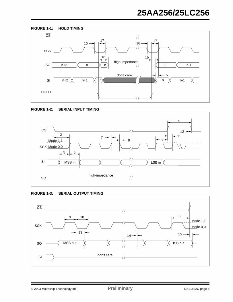
FIGURE 1-1: HOLD TIMING
FIGURE 1-2: SERIAL INPUT TIMING
FIGURE 1-3: SERIAL OUTPUT TIMING
CS
SCK
SO
SI
HOLD
1716 16
17
1918
don’t care 5
high-impedancen+2 n+1 n n-1n
n+2 n+1 n n n-1
CS
SCK
SI
SO
65
87 11
3
LSB inMSB in
high-impedance
12
Mode 1,1
Mode 0,0
2
4
CS
SCK
SO
109
13
MSB out ISB out
3
15
don’t careSI
Mode 1,1
Mode 0,0
14
25AA256/25LC256
DS21822C-page 6 Preliminary 2003 Microchip Technology Inc.
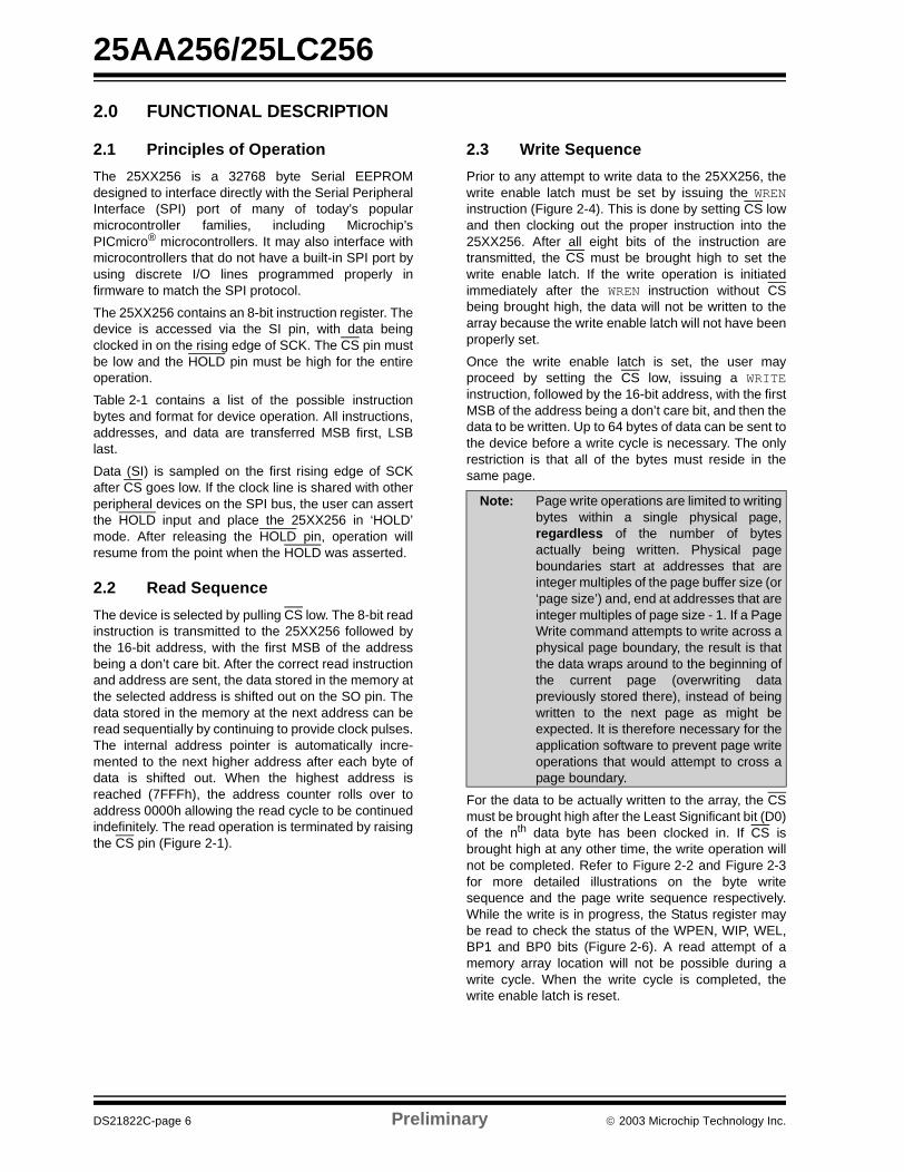
2.0 FUNCTIONAL DESCRIPTION
2.1 Principles of Operation
The 25XX256 is a 32768 byte Serial EEPROMdesigned to interface directly with the Serial PeripheralInterface (SPI) port of many of today’s popularmicrocontroller families, including Microchip’sPICmicro® microcontrollers. It may also interface withmicrocontrollers that do not have a built-in SPI port byusing discrete I/O lines programmed properly infirmware to match the SPI protocol.
The 25XX256 contains an 8-bit instruction register. Thedevice is accessed via the SI pin, with data beingclocked in on the rising edge of SCK. The CS pin mustbe low and the HOLD pin must be high for the entireoperation.
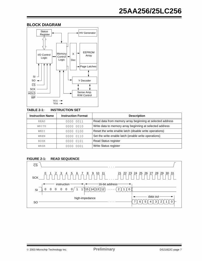
Table 2-1 contains a list of the possible instructionbytes and format for device operation. All instructions,addresses, and data are transferred MSB first, LSBlast.
Data (SI) is sampled on the first rising edge of SCKafter CS goes low. If the clock line is shared with otherperipheral devices on the SPI bus, the user can assertthe HOLD input and place the 25XX256 in ‘HOLD’mode. After releasing the HOLD pin, operation willresume from the point when the HOLD was asserted.
2.2 Read Sequence
The device is selected by pulling CS low. The 8-bit readinstruction is transmitted to the 25XX256 followed bythe 16-bit address, with the first MSB of the addressbeing a don’t care bit. After the correct read instructionand address are sent, the data stored in the memory atthe selected address is shifted out on the SO pin. Thedata stored in the memory at the next address can beread sequentially by continuing to provide clock pulses.The internal address pointer is automatically incre-mented to the next higher address after each byte ofdata is shifted out. When the highest address isreached (7FFFh), the address counter rolls over toaddress 0000h allowing the read cycle to be continuedindefinitely. The read operation is terminated by raisingthe CS pin (Figure 2-1).
2.3 Write Sequence
Prior to any attempt to write data to the 25XX256, thewrite enable latch must be set by issuing the WRENinstruction (Figure 2-4). This is done by setting CS lowand then clocking out the proper instruction into the25XX256. After all eight bits of the instruction aretransmitted, the CS must be brought high to set thewrite enable latch. If the write operation is initiatedimmediately after the WREN instruction without CSbeing brought high, the data will not be written to thearray because the write enable latch will not have beenproperly set.
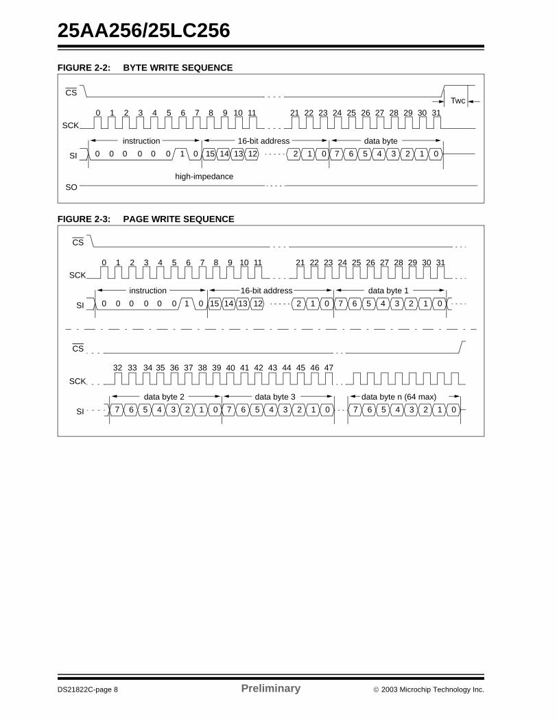
Once the write enable latch is set, the user mayproceed by setting the CS low, issuing a WRITEinstruction, followed by the 16-bit address, with the firstMSB of the address being a don’t care bit, and then thedata to be written. Up to 64 bytes of data can be sent tothe device before a write cycle is necessary. The onlyrestriction is that all of the bytes must reside in thesame page.
For the data to be actually written to the array, the CSmust be brought high after the Least Significant bit (D0)of the nth data byte has been clocked in. If CS isbrought high at any other time, the write operation willnot be completed. Refer to Figure 2-2 and Figure 2-3for more detailed illustrations on the byte writesequence and the page write sequence respectively.While the write is in progress, the Status register maybe read to check the status of the WPEN, WIP, WEL,BP1 and BP0 bits (Figure 2-6). A read attempt of amemory array location will not be possible during awrite cycle. When the write cycle is completed, thewrite enable latch is reset.
Note: Page write operations are limited to writingbytes within a single physical page,regardless of the number of bytesactually being written. Physical pageboundaries start at addresses that areinteger multiples of the page buffer size (or‘page size’) and, end at addresses that areinteger multiples of page size - 1. If a PageWrite command attempts to write across aphysical page boundary, the result is thatthe data wraps around to the beginning ofthe current page (overwriting datapreviously stored there), instead of beingwritten to the next page as might beexpected. It is therefore necessary for theapplication software to prevent page writeoperations that would attempt to cross apage boundary.
2003 Microchip Technology Inc. Preliminary DS21822C-page 7
25AA256/25LC256
BLOCK DIAGRAM
FIGURE 2-1: READ SEQUENCE
SI
SO
SCK
CS
HOLD
WP
StatusRegister
I/O Control MemoryControlLogic
X
Dec
HV Generator
EEPROMArray
Page Latches
Y Decoder
Sense Amp.R/W Control
Logic
VCCVSS
TABLE 2-1: INSTRUCTION SET
Instruction Name Instruction Format Description
READ 0000 0011 Read data from memory array beginning at selected address
WRITE 0000 0010 Write data to memory array beginning at selected address
WRDI 0000 0100 Reset the write enable latch (disable write operations)
WREN 0000 0110 Set the write enable latch (enable write operations)
RDSR 0000 0101 Read Status register
WRSR 0000 0001 Write Status register
SO
SI
SCK
CS
0 2 3 4 5 6 7 8 9 10 11 21 22 23 24 25 26 27 28 29 30 311
0 100000 1 15 14 13 12 2 1 0
7 6 5 4 3 2 1 0
instruction 16-bit address
data outhigh-impedance
25AA256/25LC256
DS21822C-page 8 Preliminary 2003 Microchip Technology Inc.
FIGURE 2-2: BYTE WRITE SEQUENCE
FIGURE 2-3: PAGE WRITE SEQUENCE
SO
SI
CS
9 10 11 21 22 23 24 25 26 27 28 29 30 31
0 000000 1 15 14 13 12 2 1 0 7 6 5 4 3 2 1 0
instruction 16-bit address data byte
high-impedance
SCK
0 2 3 4 5 6 71 8
Twc
SI
CS
9 10 11 21 22 23 24 25 26 27 28 29 30 31
0 000000 1 15 14 13 12 2 1 0 7 6 5 4 3 2 1 0
instruction 16-bit address data byte 1
SCK
0 2 3 4 5 6 71 8
SI
CS
41 42 43 46 47
7 6 5 4 3 2 1 0
data byte n (64 max)
SCK
32 34 35 36 37 38 3933 40
7 6 5 4 3 2 1 0
data byte 3
7 6 5 4 3 2 1 0
data byte 2
44 45
2003 Microchip Technology Inc. Preliminary DS21822C-page 9
25AA256/25LC256
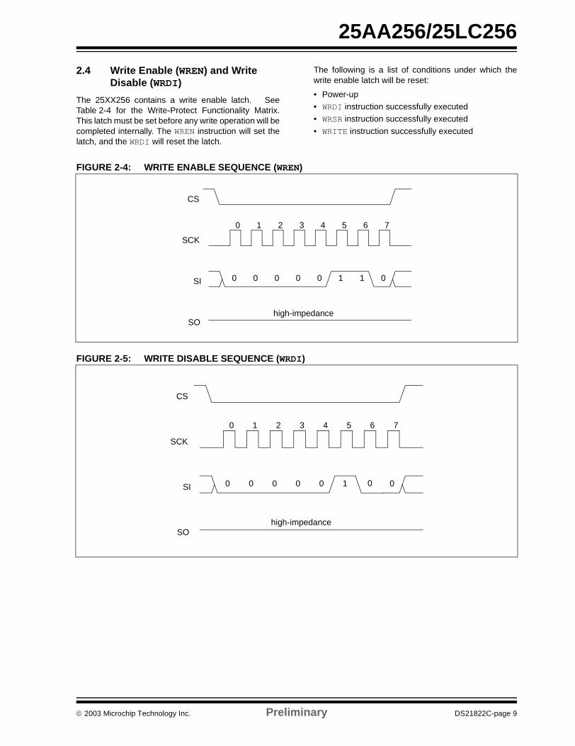
2.4 Write Enable (WREN) and Write Disable (WRDI)
The 25XX256 contains a write enable latch. SeeTable 2-4 for the Write-Protect Functionality Matrix.This latch must be set before any write operation will becompleted internally. The WREN instruction will set thelatch, and the WRDI will reset the latch.
The following is a list of conditions under which thewrite enable latch will be reset:
• Power-up• WRDI instruction successfully executed• WRSR instruction successfully executed
• WRITE instruction successfully executed
FIGURE 2-4: WRITE ENABLE SEQUENCE (WREN)
FIGURE 2-5: WRITE DISABLE SEQUENCE (WRDI)
SCK
0 2 3 4 5 6 71
SI
high-impedanceSO
CS
0 10 0 0 0 01
SCK
0 2 3 4 5 6 71
SI
high-impedanceSO
CS
0 10 0 0 0 010
25AA256/25LC256
DS21822C-page 10 Preliminary 2003 Microchip Technology Inc.
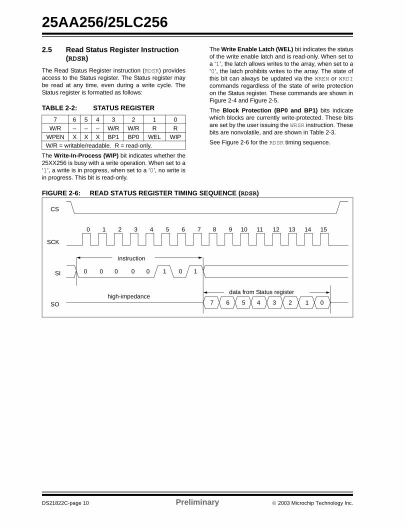
2.5 Read Status Register Instruction (RDSR)
The Read Status Register instruction (RDSR) providesaccess to the Status register. The Status register maybe read at any time, even during a write cycle. TheStatus register is formatted as follows:
TABLE 2-2: STATUS REGISTER
The Write-In-Process (WIP) bit indicates whether the25XX256 is busy with a write operation. When set to a‘1’, a write is in progress, when set to a ‘0’, no write isin progress. This bit is read-only.
The Write Enable Latch (WEL) bit indicates the statusof the write enable latch and is read-only. When set toa ‘1’, the latch allows writes to the array, when set to a‘0’, the latch prohibits writes to the array. The state ofthis bit can always be updated via the WREN or WRDIcommands regardless of the state of write protectionon the Status register. These commands are shown inFigure 2-4 and Figure 2-5.
The Block Protection (BP0 and BP1) bits indicatewhich blocks are currently write-protected. These bitsare set by the user issuing the WRSR instruction. Thesebits are nonvolatile, and are shown in Table 2-3.
See Figure 2-6 for the RDSR timing sequence.
FIGURE 2-6: READ STATUS REGISTER TIMING SEQUENCE (RDSR)
7 6 5 4 3 2 1 0
W/R – – – W/R W/R R RWPEN X X X BP1 BP0 WEL WIPW/R = writable/readable. R = read-only.
SO
SI
CS
9 10 11 12 13 14 15
1 100000 0
7 6 5 4 2 1 0
instruction
data from Status registerhigh-impedance
SCK
0 2 3 4 5 6 71 8
3
2003 Microchip Technology Inc. Preliminary DS21822C-page 11
25AA256/25LC256
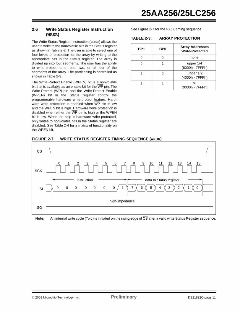
2.6 Write Status Register Instruction (WRSR)
The Write Status Register instruction (WRSR) allows theuser to write to the nonvolatile bits in the Status registeras shown in Table 2-2. The user is able to select one offour levels of protection for the array by writing to theappropriate bits in the Status register. The array isdivided up into four segments. The user has the abilityto write-protect none, one, two, or all four of thesegments of the array. The partitioning is controlled asshown in Table 2-3.
The Write-Protect Enable (WPEN) bit is a nonvolatilebit that is available as an enable bit for the WP pin. TheWrite-Protect (WP) pin and the Write-Protect Enable(WPEN) bit in the Status register control theprogrammable hardware write-protect feature. Hard-ware write protection is enabled when WP pin is lowand the WPEN bit is high. Hardware write protection isdisabled when either the WP pin is high or the WPENbit is low. When the chip is hardware write-protected,only writes to nonvolatile bits in the Status register aredisabled. See Table 2-4 for a matrix of functionality onthe WPEN bit.
See Figure 2-7 for the WRSR timing sequence.
TABLE 2-3: ARRAY PROTECTION
FIGURE 2-7: WRITE STATUS REGISTER TIMING SEQUENCE (WRSR)
BP1 BP0Array AddressesWrite-Protected
0 0 none
0 1 upper 1/4(6000h - 7FFFh)
1 0 upper 1/2(4000h - 7FFFh)
1 1 all(0000h - 7FFFh)
SO
SI
CS
9 10 11 12 13 14 15
0 100000 0 7 6 5 4 2 1 0
instruction data to Status register
high-impedance
SCK
0 2 3 4 5 6 71 8
3
Note: An internal write cycle (TWC) is initiated on the rising edge of CS after a valid write Status Register sequence.
25AA256/25LC256
DS21822C-page 12 Preliminary 2003 Microchip Technology Inc.
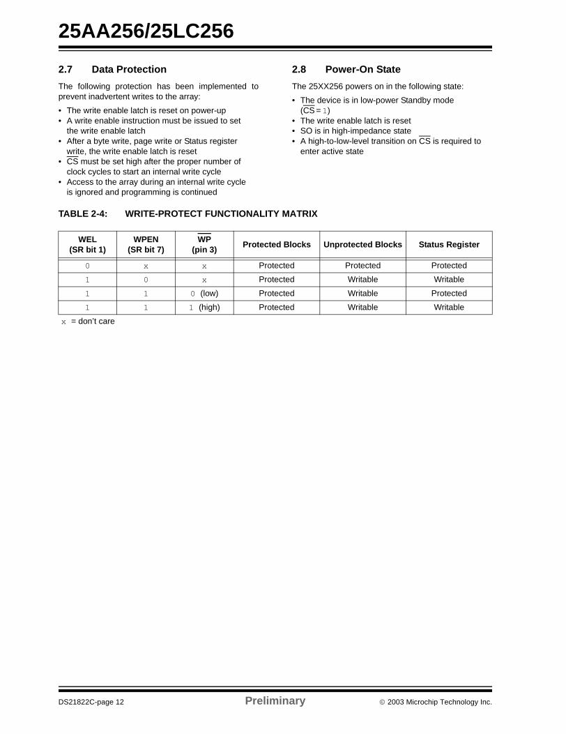
2.7 Data Protection
The following protection has been implemented toprevent inadvertent writes to the array:
• The write enable latch is reset on power-up• A write enable instruction must be issued to set
the write enable latch• After a byte write, page write or Status register
write, the write enable latch is reset• CS must be set high after the proper number of
clock cycles to start an internal write cycle• Access to the array during an internal write cycle
is ignored and programming is continued
2.8 Power-On State
The 25XX256 powers on in the following state:
• The device is in low-power Standby mode (CS =1)
• The write enable latch is reset• SO is in high-impedance state• A high-to-low-level transition on CS is required to
enter active state
TABLE 2-4: WRITE-PROTECT FUNCTIONALITY MATRIX
WEL(SR bit 1)
WPEN(SR bit 7)
WP(pin 3)
Protected Blocks Unprotected Blocks Status Register
0 x x Protected Protected Protected
1 0 x Protected Writable Writable
1 1 0 (low) Protected Writable Protected
1 1 1 (high) Protected Writable Writable
x = don’t care
2003 Microchip Technology Inc. Preliminary DS21822C-page 13
25AA256/25LC256
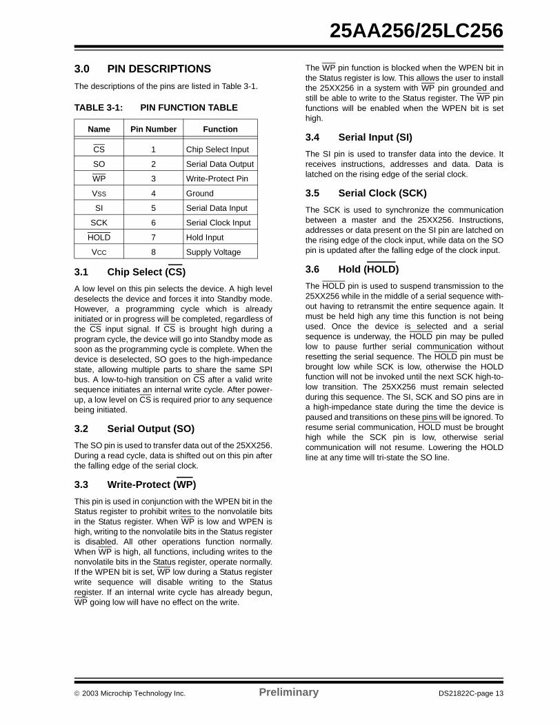
3.0 PIN DESCRIPTIONS
The descriptions of the pins are listed in Table 3-1.
TABLE 3-1: PIN FUNCTION TABLE
3.1 Chip Select (CS)
A low level on this pin selects the device. A high leveldeselects the device and forces it into Standby mode.However, a programming cycle which is alreadyinitiated or in progress will be completed, regardless ofthe CS input signal. If CS is brought high during aprogram cycle, the device will go into Standby mode assoon as the programming cycle is complete. When thedevice is deselected, SO goes to the high-impedancestate, allowing multiple parts to share the same SPIbus. A low-to-high transition on CS after a valid writesequence initiates an internal write cycle. After power-up, a low level on CS is required prior to any sequencebeing initiated.
3.2 Serial Output (SO)
The SO pin is used to transfer data out of the 25XX256.During a read cycle, data is shifted out on this pin afterthe falling edge of the serial clock.
3.3 Write-Protect (WP)
This pin is used in conjunction with the WPEN bit in theStatus register to prohibit writes to the nonvolatile bitsin the Status register. When WP is low and WPEN ishigh, writing to the nonvolatile bits in the Status registeris disabled. All other operations function normally.When WP is high, all functions, including writes to thenonvolatile bits in the Status register, operate normally.If the WPEN bit is set, WP low during a Status registerwrite sequence will disable writing to the Statusregister. If an internal write cycle has already begun,WP going low will have no effect on the write.
The WP pin function is blocked when the WPEN bit inthe Status register is low. This allows the user to installthe 25XX256 in a system with WP pin grounded andstill be able to write to the Status register. The WP pinfunctions will be enabled when the WPEN bit is sethigh.
3.4 Serial Input (SI)
The SI pin is used to transfer data into the device. Itreceives instructions, addresses and data. Data islatched on the rising edge of the serial clock.
3.5 Serial Clock (SCK)
The SCK is used to synchronize the communicationbetween a master and the 25XX256. Instructions,addresses or data present on the SI pin are latched onthe rising edge of the clock input, while data on the SOpin is updated after the falling edge of the clock input.
3.6 Hold (HOLD)
The HOLD pin is used to suspend transmission to the25XX256 while in the middle of a serial sequence with-out having to retransmit the entire sequence again. Itmust be held high any time this function is not beingused. Once the device is selected and a serialsequence is underway, the HOLD pin may be pulledlow to pause further serial communication withoutresetting the serial sequence. The HOLD pin must bebrought low while SCK is low, otherwise the HOLDfunction will not be invoked until the next SCK high-to-low transition. The 25XX256 must remain selectedduring this sequence. The SI, SCK and SO pins are ina high-impedance state during the time the device ispaused and transitions on these pins will be ignored. Toresume serial communication, HOLD must be broughthigh while the SCK pin is low, otherwise serialcommunication will not resume. Lowering the HOLDline at any time will tri-state the SO line.
Name Pin Number Function
CS 1 Chip Select Input
SO 2 Serial Data Output
WP 3 Write-Protect Pin
VSS 4 Ground
SI 5 Serial Data Input
SCK 6 Serial Clock Input
HOLD 7 Hold Input
VCC 8 Supply Voltage
25AA256/25LC256
DS21822C-page 14 Preliminary 2003 Microchip Technology Inc.
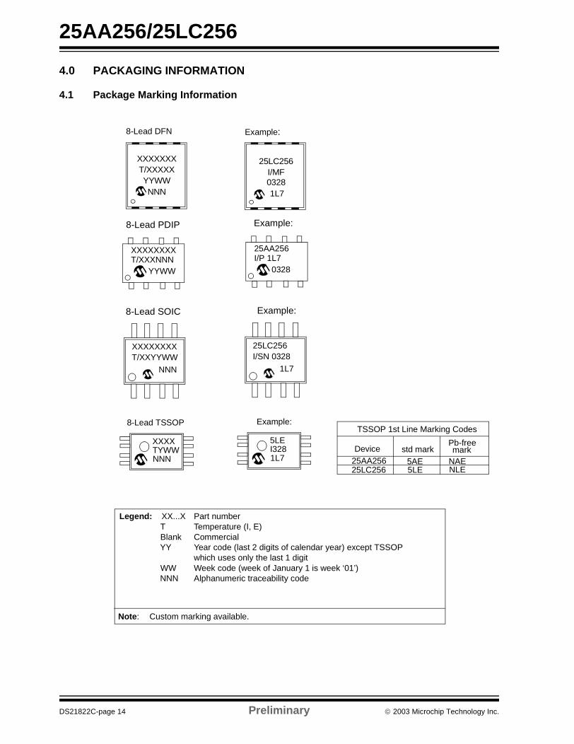
4.0 PACKAGING INFORMATION
4.1 Package Marking Information
Legend: XX...X Part numberT Temperature (I, E)Blank CommercialYY Year code (last 2 digits of calendar year) except TSSOP which uses only the last 1 digitWW Week code (week of January 1 is week ‘01’)NNN Alphanumeric traceability code
Note: Custom marking available.
T/XXXNNNXXXXXXXX
YYWW
8-Lead PDIP
8-Lead SOIC
T/XXYYWWXXXXXXXX
NNN
XXXXTYWW
8-Lead TSSOP
NNN
I/P 1L725AA256
0328
Example:
Example:
I/SN 032825LC256
1L7
1L7
5LEI328
Example:TSSOP 1st Line Marking Codes
Device25AA256
std markPb-freemark
5AE NAE
8-Lead DFN Example:
XXXXXXXT/XXXXXYYWW
25LC256I/MF03281L7NNN
25LC256 5LE NLE
2003 Microchip Technology Inc. Preliminary DS21822C-page 15
25AA256/25LC256
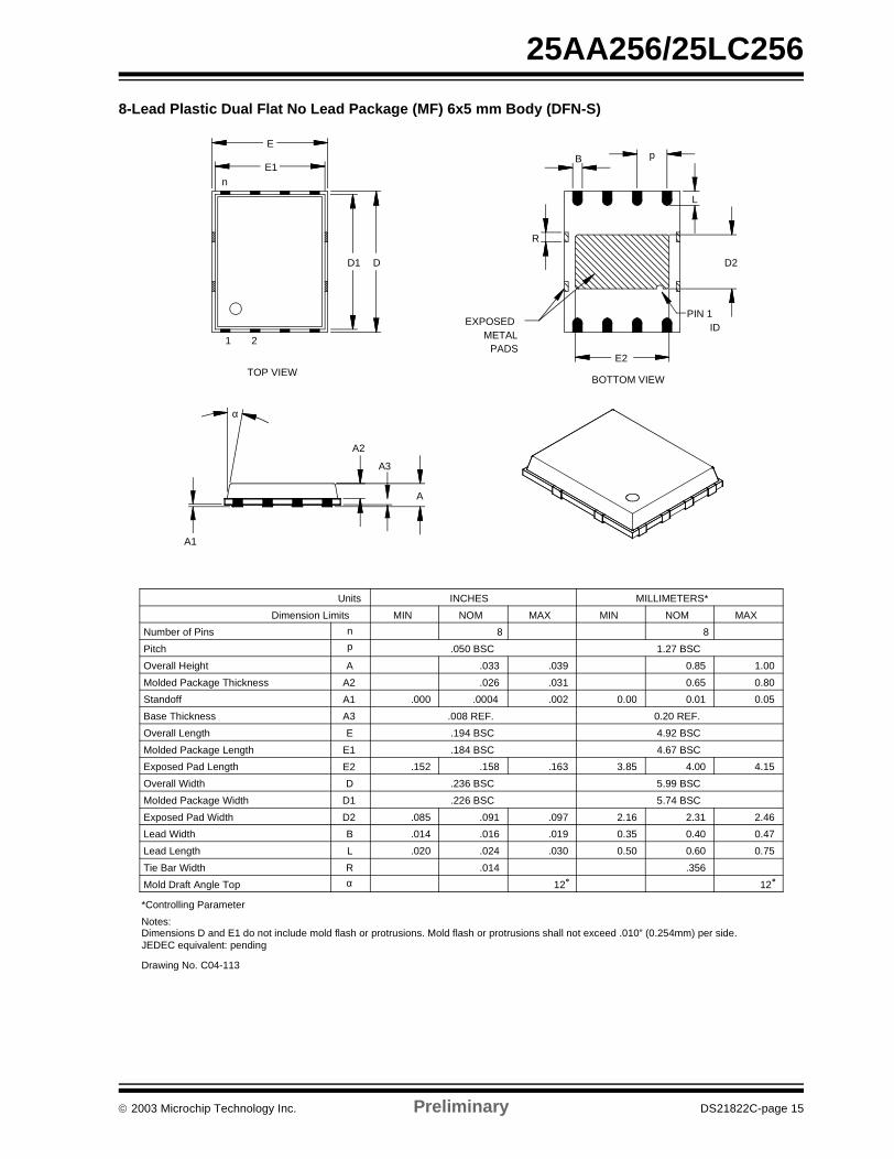
8-Lead Plastic Dual Flat No Lead Package (MF) 6x5 mm Body (DFN-S)
NOM
.050 BSC
INCHES
.194 BSC
.184 BSC
.226 BSC
.236 BSC
.008 REF.
DOverall Width
JEDEC equivalent: pending
Notes:
Drawing No. C04-113
Molded Package Width
Lead Width
*Controlling Parameter
Mold Draft Angle Top
Tie Bar Width
Lead Length
R
α
B
L
D1
.014
.020
Dimension Limits
Molded Package Thickness
Pitch
Overall Height
Overall Length
Molded Package Length
Base Thickness
Standoff
Number of Pins
A3
E1
E
A2
A1
A
.000
Units
n
p
MIN
TOP VIEW
1 2
A2
A
5.99 BSC
.019
12
.030
.014
.016
.024
0.35
0.50
.356
0.40
0.60
5.74 BSC
12
0.47
0.75
MILLIMETERS*
.039
.002
.031.026
.0004
.033
0.00
8
MAX MIN
1.27 BSC
0.20 REF.
4.92 BSC
4.67 BSC
0.85
0.01
0.65 0.80
0.05
1.00
MAXNOM
8
BOTTOM VIEW
n
E
E1
PIN 1
pB
Exposed Pad Length E2
Exposed Pad Width D2 .085 .091 .097 2.16 2.31 2.46
.152 .158 .163 3.85 4.00 4.15
EXPOSEDMETAL
PADS
D2
E2
A1
A3
α
L
ID
D1 D
R
Dimensions D and E1 do not include mold flash or protrusions. Mold flash or protrusions shall not exceed .010” (0.254mm) per side.
25AA256/25LC256
DS21822C-page 16 Preliminary 2003 Microchip Technology Inc.
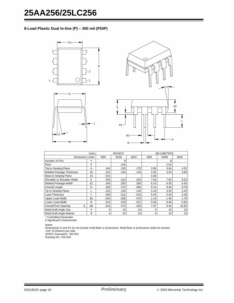
8-Lead Plastic Dual In-line (P) – 300 mil (PDIP)
B1
B
A1
A
L
A2
p
α
E
eB
β
c
E1
n
D
1
2
Units INCHES* MILLIMETERSDimension Limits MIN NOM MAX MIN NOM MAX
Number of Pins n 8 8Pitch p .100 2.54Top to Seating Plane A .140 .155 .170 3.56 3.94 4.32Molded Package Thickness A2 .115 .130 .145 2.92 3.30 3.68Base to Seating Plane A1 .015 0.38Shoulder to Shoulder Width E .300 .313 .325 7.62 7.94 8.26Molded Package Width E1 .240 .250 .260 6.10 6.35 6.60Overall Length D .360 .373 .385 9.14 9.46 9.78Tip to Seating Plane L .125 .130 .135 3.18 3.30 3.43Lead Thickness c .008 .012 .015 0.20 0.29 0.38Upper Lead Width B1 .045 .058 .070 1.14 1.46 1.78Lower Lead Width B .014 .018 .022 0.36 0.46 0.56Overall Row Spacing § eB .310 .370 .430 7.87 9.40 10.92Mold Draft Angle Top α 5 10 15 5 10 15Mold Draft Angle Bottom β 5 10 15 5 10 15* Controlling Parameter
Notes:Dimensions D and E1 do not include mold flash or protrusions. Mold flash or protrusions shall not exceed
JEDEC Equivalent: MS-001Drawing No. C04-018
.010” (0.254mm) per side.
§ Significant Characteristic
2003 Microchip Technology Inc. Preliminary DS21822C-page 17
25AA256/25LC256
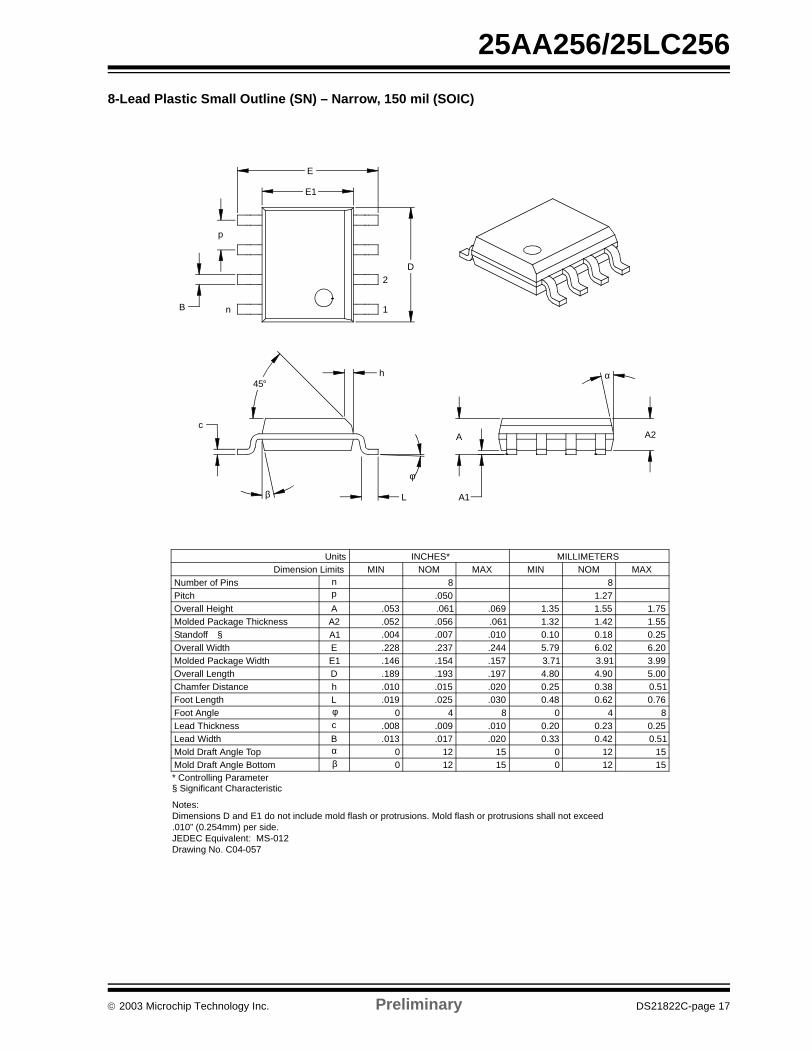
8-Lead Plastic Small Outline (SN) – Narrow, 150 mil (SOIC)
Foot Angle φ 0 4 8 0 4 8
1512015120βMold Draft Angle Bottom1512015120αMold Draft Angle Top
0.510.420.33.020.017.013BLead Width0.250.230.20.010.009.008cLead Thickness
0.760.620.48.030.025.019LFoot Length0.510.380.25.020.015.010hChamfer Distance5.004.904.80.197.193.189DOverall Length3.993.913.71.157.154.146E1Molded Package Width6.206.025.79.244.237.228EOverall Width0.250.180.10.010.007.004A1Standoff §1.551.421.32.061.056.052A2Molded Package Thickness1.751.551.35.069.061.053AOverall Height
1.27.050pPitch88nNumber of Pins
MAXNOMMINMAXNOMMINDimension LimitsMILLIMETERSINCHES*Units
2
1
D
n
p
B
E
E1
h
Lβ
c
45°
φ
A2
α
A
A1
* Controlling Parameter
Notes:Dimensions D and E1 do not include mold flash or protrusions. Mold flash or protrusions shall not exceed .010” (0.254mm) per side.JEDEC Equivalent: MS-012Drawing No. C04-057
§ Significant Characteristic
25AA256/25LC256
DS21822C-page 18 Preliminary 2003 Microchip Technology Inc.
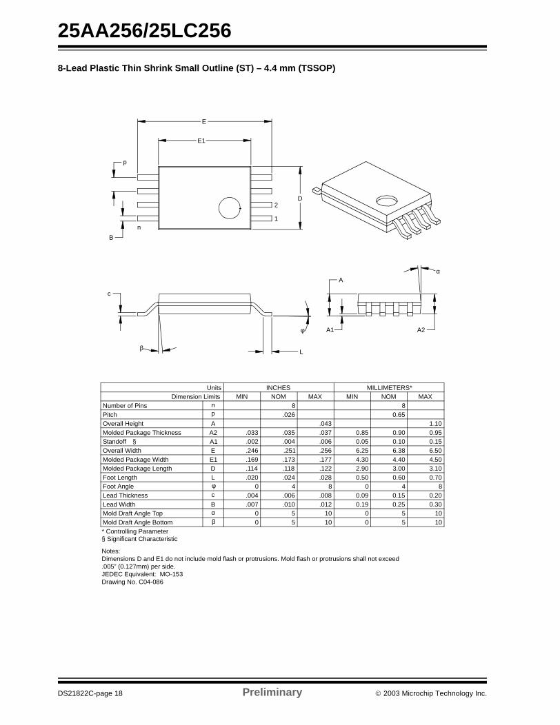
8-Lead Plastic Thin Shrink Small Outline (ST) – 4.4 mm (TSSOP)
10501050βMold Draft Angle Bottom10501050αMold Draft Angle Top
0.300.250.19.012.010.007BLead Width0.200.150.09.008.006.004cLead Thickness
0.700.600.50.028.024.020LFoot Length3.103.002.90.122.118.114DMolded Package Length4.504.404.30.177.173.169E1Molded Package Width6.506.386.25.256.251.246EOverall Width0.150.100.05.006.004.002A1Standoff §0.950.900.85.037.035.033A2Molded Package Thickness1.10.043AOverall Height
0.65.026pPitch88nNumber of Pins
MAXNOMMINMAXNOMMINDimension LimitsMILLIMETERS*INCHESUnits
α
A2
A
A1
L
c
β
φ
1
2D
n
p
B
E
E1
Foot Angle φ 0 4 8 0 4 8
* Controlling Parameter
Notes:Dimensions D and E1 do not include mold flash or protrusions. Mold flash or protrusions shall not exceed .005” (0.127mm) per side.JEDEC Equivalent: MO-153Drawing No. C04-086
§ Significant Characteristic
2003 Microchip Technology Inc. Preliminary DS21822C-page 19
25AA256/25LC256
APPENDIX A: REVISION HISTORY
Revision C
Corrections to Section 1.0, Electrical Characteristics.

25AA256/25LC256
DS21822C-page 20 Preliminary 2003 Microchip Technology Inc.
NOTES:
2003 Microchip Technology Inc. Preliminary DS21822C-page 21
25AA256/25LC256
ON-LINE SUPPORT
Microchip provides on-line support on the MicrochipWorld Wide Web site.
The web site is used by Microchip as a means to makefiles and information easily available to customers. Toview the site, the user must have access to the Internetand a web browser, such as Netscape® or Microsoft®
Internet Explorer. Files are also available for FTPdownload from our FTP site.
Connecting to the Microchip Internet Web Site
The Microchip web site is available at the followingURL:
www.microchip.com
The file transfer site is available by using an FTPservice to connect to:
ftp://ftp.microchip.com
The web site and file transfer site provide a variety ofservices. Users may download files for the latestDevelopment Tools, Data Sheets, Application Notes,User's Guides, Articles and Sample Programs. Avariety of Microchip specific business information isalso available, including listings of Microchip salesoffices, distributors and factory representatives. Otherdata available for consideration is:
• Latest Microchip Press Releases• Technical Support Section with Frequently Asked
Questions • Design Tips
• Device Errata• Job Postings• Microchip Consultant Program Member Listing
• Links to other useful web sites related to Microchip Products
• Conferences for products, Development Systems, technical information and more
• Listing of seminars and events
SYSTEMS INFORMATION AND UPGRADE HOT LINE
The Systems Information and Upgrade Line providessystem users a listing of the latest versions of all ofMicrochip's development systems software products.Plus, this line provides information on how customerscan receive the most current upgrade kits.The Hot LineNumbers are:
1-800-755-2345 for U.S. and most of Canada, and
1-480-792-7302 for the rest of the world.
042003

25AA256/25LC256
DS21822C-page 22 Preliminary 2003 Microchip Technology Inc.
READER RESPONSE
It is our intention to provide you with the best documentation possible to ensure successful use of your Microchip prod-uct. If you wish to provide your comments on organization, clarity, subject matter, and ways in which our documentationcan better serve you, please FAX your comments to the Technical Publications Manager at (480) 792-4150.
Please list the following information, and use this outline to provide us with your comments about this document.
To: Technical Publications Manager
RE: Reader Response
Total Pages Sent ________
From: Name
Company
Address
City / State / ZIP / Country
Telephone: (_______) _________ - _________
Application (optional):
Would you like a reply? Y N
Device: Literature Number:
Questions:
FAX: (______) _________ - _________
DS21822C25AA256/25LC256
1. What are the best features of this document?
2. How does this document meet your hardware and software development needs?
3. Do you find the organization of this document easy to follow? If not, why?
4. What additions to the document do you think would enhance the structure and subject?
5. What deletions from the document could be made without affecting the overall usefulness?
6. Is there any incorrect or misleading information (what and where)?
7. How would you improve this document?
2003 Microchip Technology Inc. Preliminary DS21822C-page 23
25AA256/25LC256
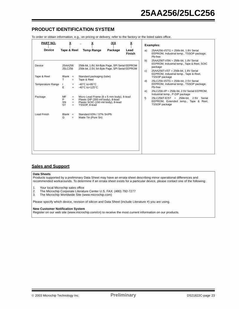
PRODUCT IDENTIFICATION SYSTEM
To order or obtain information, e.g., on pricing or delivery, refer to the factory or the listed sales office.
Sales and Support
PART NO. X /XX X
Lead PackageTape & ReelDevice
Device 25AA25625LC256
256k-bit, 1.8V, 64-Byte Page, SPI Serial EEPROM256k-bit, 2.5V, 64-Byte Page, SPI Serial EEPROM
Tape & Reel Blank = T =
Standard packaging (tube)Tape & Reel
Temperature Range I =E =
-40°C to+85°C-40°C to+125°C
Package MF =P =SN =ST =
Micro Lead Frame (6 x 5 mm body), 8-leadPlastic DIP (300 mil body), 8-leadPlastic SOIC (150 mil body), 8-leadTSSOP, 8-lead
Lead Finish Blank =G =
Standard 63% / 37% Sn/PbMatte Tin (Pure Sn)
Examples:
a) 25AA256-I/STG = 256k-bit, 1.8V Serial EEPROM, Industrial temp., TSSOP package, Pb-free
b) 25AA256T-I/SN = 256k-bit, 1.8V Serial EEPROM, Industrial temp., Tape & Reel, SOIC package
c) 25AA256T-I/ST = 256k-bit, 1.8V Serial EEPROM, Industrial temp., Tape & Reel, TSSOP package
d) 25LC256-I/STG = 256k-bit, 2.5V Serial EEPROM, Industrial temp., TSSOP package, Pb-free
e) 25LC256-I/P = 256k-bit, 2.5V Serial EEPROM, Industrial temp., P-DIP package
f) 25LC256T-E/ST = 256k-bit, 2.5V SerialEEPROM, Extended temp., Tape & Reel,TSSOP package
–
Finish
Data SheetsProducts supported by a preliminary Data Sheet may have an errata sheet describing minor operational differences and recommended workarounds. To determine if an errata sheet exists for a particular device, please contact one of the following:
1. Your local Microchip sales office2. The Microchip Corporate Literature Center U.S. FAX: (480) 792-72773. The Microchip Worldwide Site (www.microchip.com)
Please specify which device, revision of silicon and Data Sheet (include Literature #) you are using.
New Customer Notification SystemRegister on our web site (www.microchip.com/cn) to receive the most current information on our products.
X
Temp Range
25AA256/25LC256
DS21822C-page 24 Preliminary 2003 Microchip Technology Inc.
NOTES:
2003 Microchip Technology Inc. Preliminary DS21822C-page 25
Information contained in this publication regarding deviceapplications and the like is intended through suggestion onlyand may be superseded by updates. It is your responsibility toensure that your application meets with your specifications.No representation or warranty is given and no liability isassumed by Microchip Technology Incorporated with respectto the accuracy or use of such information, or infringement ofpatents or other intellectual property rights arising from suchuse or otherwise. Use of Microchip’s products as critical com-ponents in life support systems is not authorized except withexpress written approval by Microchip. No licenses are con-veyed, implicitly or otherwise, under any intellectual propertyrights.
Trademarks
The Microchip name and logo, the Microchip logo, Accuron,dsPIC, KEELOQ, MPLAB, PIC, PICmicro, PICSTART, PRO MATE and PowerSmart are registered trademarks ofMicrochip Technology Incorporated in the U.S.A. and othercountries.
AmpLab, FilterLab, microID, MXDEV, MXLAB, PICMASTER,SEEVAL and The Embedded Control Solutions Company areregistered trademarks of Microchip Technology Incorporatedin the U.S.A.
Application Maestro, dsPICDEM, dsPICDEM.net, ECAN,ECONOMONITOR, FanSense, FlexROM, fuzzyLAB, In-Circuit Serial Programming, ICSP, ICEPIC, microPort,Migratable Memory, MPASM, MPLIB, MPLINK, MPSIM,PICkit, PICDEM, PICDEM.net, PowerCal, PowerInfo,PowerMate, PowerTool, rfLAB, rfPIC, Select Mode,SmartSensor, SmartShunt, SmartTel and Total Endurance aretrademarks of Microchip Technology Incorporated in theU.S.A. and other countries.
Serialized Quick Turn Programming (SQTP) is a service markof Microchip Technology Incorporated in the U.S.A.
All other trademarks mentioned herein are property of theirrespective companies.
© 2003, Microchip Technology Incorporated, Printed in theU.S.A., All Rights Reserved.
Printed on recycled paper.
Note the following details of the code protection feature on Microchip devices:
• Microchip products meet the specification contained in their particular Microchip Data Sheet.
• Microchip believes that its family of products is one of the most secure families of its kind on the market today, when used in the intended manner and under normal conditions.
• There are dishonest and possibly illegal methods used to breach the code protection feature. All of these methods, to our knowledge, require using the Microchip products in a manner outside the operating specifications contained in Microchip's Data Sheets. Most likely, the person doing so is engaged in theft of intellectual property.
• Microchip is willing to work with the customer who is concerned about the integrity of their code.
• Neither Microchip nor any other semiconductor manufacturer can guarantee the security of their code. Code protection does not mean that we are guaranteeing the product as “unbreakable.”
Code protection is constantly evolving. We at Microchip are committed to continuously improving the code protection features of ourproducts. Attempts to break microchip’s code protection feature may be a violation of the Digital Millennium Copyright Act. If such actsallow unauthorized access to your software or other copyrighted work, you may have a right to sue for relief under that Act.
Microchip received QS-9000 quality system certification for its worldwide headquarters, design and wafer fabrication facilities in Chandler and Tempe, Arizona in July 1999 and Mountain View, California in March 2002. The Company’s quality system processes and procedures are QS-9000 compliant for its PICmicro® 8-bit MCUs, KEELOQ® code hopping devices, Serial EEPROMs, microperipherals, non-volatile memory and analog products. In addition, Microchip’s quality system for the design and manufacture of development systems is ISO 9001 certified.
DS21822C-page 26 Preliminary 2003 Microchip Technology Inc.
AMERICASCorporate Office2355 West Chandler Blvd.Chandler, AZ 85224-6199Tel: 480-792-7200 Fax: 480-792-7277Technical Support: 480-792-7627Web Address: http://www.microchip.com
Atlanta3780 Mansell Road, Suite 130Alpharetta, GA 30022Tel: 770-640-0034 Fax: 770-640-0307
Boston2 Lan Drive, Suite 120Westford, MA 01886Tel: 978-692-3848 Fax: 978-692-3821
Chicago333 Pierce Road, Suite 180Itasca, IL 60143Tel: 630-285-0071 Fax: 630-285-0075
Dallas4570 Westgrove Drive, Suite 160Addison, TX 75001Tel: 972-818-7423 Fax: 972-818-2924
DetroitTri-Atria Office Building 32255 Northwestern Highway, Suite 190Farmington Hills, MI 48334Tel: 248-538-2250Fax: 248-538-2260
Kokomo2767 S. Albright Road Kokomo, IN 46902Tel: 765-864-8360Fax: 765-864-8387
Los Angeles18201 Von Karman, Suite 1090Irvine, CA 92612Tel: 949-263-1888 Fax: 949-263-1338
Phoenix2355 West Chandler Blvd.Chandler, AZ 85224-6199Tel: 480-792-7966 Fax: 480-792-4338
San Jose2107 North First Street, Suite 590San Jose, CA 95131Tel: 408-436-7950 Fax: 408-436-7955
Toronto6285 Northam Drive, Suite 108Mississauga, Ontario L4V 1X5, CanadaTel: 905-673-0699 Fax: 905-673-6509
ASIA/PACIFICAustraliaSuite 22, 41 Rawson StreetEpping 2121, NSWAustraliaTel: 61-2-9868-6733 Fax: 61-2-9868-6755China - BeijingUnit 915Bei Hai Wan Tai Bldg.No. 6 Chaoyangmen Beidajie Beijing, 100027, No. ChinaTel: 86-10-85282100 Fax: 86-10-85282104China - ChengduRm. 2401-2402, 24th Floor, Ming Xing Financial TowerNo. 88 TIDU StreetChengdu 610016, ChinaTel: 86-28-86766200 Fax: 86-28-86766599China - FuzhouUnit 28F, World Trade PlazaNo. 71 Wusi RoadFuzhou 350001, ChinaTel: 86-591-7503506 Fax: 86-591-7503521China - Hong Kong SARUnit 901-6, Tower 2, Metroplaza223 Hing Fong RoadKwai Fong, N.T., Hong KongTel: 852-2401-1200 Fax: 852-2401-3431China - ShanghaiRoom 701, Bldg. BFar East International PlazaNo. 317 Xian Xia RoadShanghai, 200051Tel: 86-21-6275-5700 Fax: 86-21-6275-5060China - ShenzhenRm. 1812, 18/F, Building A, United PlazaNo. 5022 Binhe Road, Futian DistrictShenzhen 518033, ChinaTel: 86-755-82901380 Fax: 86-755-8295-1393China - ShundeRoom 401, Hongjian BuildingNo. 2 Fengxiangnan Road, Ronggui TownShunde City, Guangdong 528303, ChinaTel: 86-765-8395507 Fax: 86-765-8395571China - QingdaoRm. B505A, Fullhope Plaza,No. 12 Hong Kong Central Rd.Qingdao 266071, ChinaTel: 86-532-5027355 Fax: 86-532-5027205IndiaDivyasree Chambers1 Floor, Wing A (A3/A4)No. 11, O’Shaugnessey RoadBangalore, 560 025, IndiaTel: 91-80-2290061 Fax: 91-80-2290062JapanBenex S-1 6F3-18-20, ShinyokohamaKohoku-Ku, Yokohama-shiKanagawa, 222-0033, JapanTel: 81-45-471- 6166 Fax: 81-45-471-6122
Korea168-1, Youngbo Bldg. 3 FloorSamsung-Dong, Kangnam-KuSeoul, Korea 135-882Tel: 82-2-554-7200 Fax: 82-2-558-5932 or 82-2-558-5934Singapore200 Middle Road#07-02 Prime CentreSingapore, 188980Tel: 65-6334-8870 Fax: 65-6334-8850TaiwanKaohsiung Branch30F - 1 No. 8Min Chuan 2nd RoadKaohsiung 806, TaiwanTel: 886-7-536-4818Fax: 886-7-536-4803TaiwanTaiwan Branch11F-3, No. 207Tung Hua North RoadTaipei, 105, TaiwanTel: 886-2-2717-7175 Fax: 886-2-2545-0139
EUROPEAustriaDurisolstrasse 2A-4600 WelsAustriaTel: 43-7242-2244-399Fax: 43-7242-2244-393DenmarkRegus Business CentreLautrup hoj 1-3Ballerup DK-2750 DenmarkTel: 45-4420-9895 Fax: 45-4420-9910FranceParc d’Activite du Moulin de Massy43 Rue du Saule TrapuBatiment A - ler Etage91300 Massy, FranceTel: 33-1-69-53-63-20 Fax: 33-1-69-30-90-79GermanySteinheilstrasse 10D-85737 Ismaning, GermanyTel: 49-89-627-144-0 Fax: 49-89-627-144-44ItalyVia Quasimodo, 1220025 Legnano (MI)Milan, Italy Tel: 39-0331-742611 Fax: 39-0331-466781NetherlandsP. A. De Biesbosch 14NL-5152 SC Drunen, NetherlandsTel: 31-416-690399 Fax: 31-416-690340United Kingdom505 Eskdale RoadWinnersh TriangleWokingham Berkshire, England RG41 5TUTel: 44-118-921-5869Fax: 44-118-921-5820
07/28/03
WORLDWIDE SALES AND SERVICE
Mouser Electronics
Authorized Distributor
Click to View Pricing, Inventory, Delivery & Lifecycle Information: Microchip:
25LC256-E/MF 25LC256-E/ST 25LC256-E/SN 25AA256-I/P 25AA256T-I/SN 25AA256T-I/ST 25AA256-I/MF
25AA256T-I/MF 25AA256-I/ST 25AA256-I/SN 25LC256T-E/ST 25LC256T-E/SN 25LC256-I/P 25LC256-I/MF
25LC256-I/SN 25LC256-E/P 25LC256T-I/SN 25LC256T-I/MF 25LC256T-I/ST 25LC256T-E/MF 25LC256-I/ST


![[XLS] · Web view3" графическая 160*32 точек, 256K FLASH, порты COM1/COM2, без батареи TP04G-AS2 3" графическая 128*64 точек, 256K FLASH,](https://img.pdfslide.net/doc/110x75/5b3b701e7f8b9ace408ca5e5/xls-web-view3-16032-256k-flash-.jpg)