Embed Size (px)
Citation preview

Support Note No. 289, Rev. A
Scanning Capacitance Microscopy (SCM)
© Digital Instruments Veec112 Robin Hill Rd. Santa Barbara, CA 93117(805)967-1400
Rev.
Rev. A
289.1 Introduction
This support note describes scanning capacitance microscopy (SCM) for the imaging of two-dimensional carrier profiles in semiconductor devices and materials. It includes specific directions for obtaining SCM images with the Digital Instruments, Veeco SCM application module.
SCM enables AFM users to measure small capacitance variations on semiconductor samples with a high spatial resolution (< 15 nm). A user applies a selectable AC and DC bias between the sample and the conductive tip, with the tip being on virtual ground. The tip and sample form a small metal-insulator-semiconductor (MIS) capacitor, whose capacitance value monitors using a high-frequency resonant circuit while the tip scans in contact mode. In this way, you obtain an image of the sample’s topography and capacitance variation simultaneously, enabling the direct correlation of a sample location with its electrical properties. An important application of SCM is to measure the two-dimensional distribution of electrical carriers inside semiconductor devices. This support includes:
• SCM Instrumentation: Section 289.2
• Safety Precautions: Section 289.3
• Theory of Operation: Section 289.4
• Installation/Setup of the SCM: Section 289.5
• SCM Imaging/Collecting Data: Section 289.6
• Sweeping: Section 289.7
• Sample Preparation for SCM: Section 289.8
• Troubleshooting: Section 289.9
o Metrology, 2000 289-1
Document Revision History: Support Note 289
Date Sections Ref. DCR Approval
01/31/00 Preliminary Release 0332 K. Slater
Scanning Capacitance Microscopy (SCM) Support Note No. 289
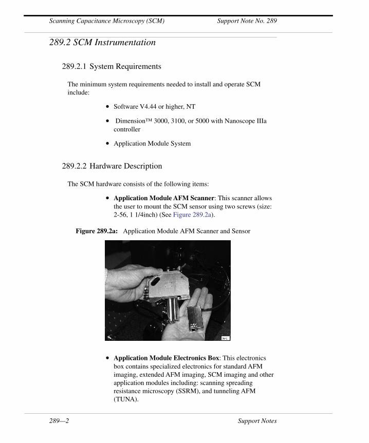
289.2 SCM Instrumentation
289.2.1 System Requirements
The minimum system requirements needed to install and operate SCM include:
• Software V4.44 or higher, NT
• Dimension™ 3000, 3100, or 5000 with Nanoscope IIIa controller
• Application Module System
289.2.2 Hardware Description
The SCM hardware consists of the following items:
• Application Module AFM Scanner: This scanner allows the user to mount the SCM sensor using two screws (size: 2-56, 1 1/4inch) (See Figure 289.2a).
Figure 289.2a: Application Module AFM Scanner and Sensor
• Application Module Electronics Box: This electronics box contains specialized electronics for standard AFM imaging, extended AFM imaging, SCM imaging and other application modules including: scanning spreading resistance microscopy (SSRM), and tunneling AFM (TUNA).
289—2 Support Notes

Support Note No.289 Scanning Capacitance Microscopy (SCM)
SCM Instrumentation continued...
• SCM Sensor: You may mount the SCM sensor on the application module AFM scanner using two screws. The SCM sensor contains the resonance circuit necessary for capacitance imaging. It connects to the application module electronics box using the subminiature D-15 connector (See Figure 289.2b).
Figure 289.2b: Mounting of the Sensor on the Application Module AFM Scanner
• The SCM Tip Holder: Provides electrical connection from the tip to the SCM sensor, while maintaining standard features for contact mode and tapping mode imaging (See Figure 289.2c).
Figure 289.2c: SCM Tip Holder
Note: Using the application module AFM scanner and electronics box, you can operate other application modules such as SSRM and TUNA, provided that you have the corresponding sensor and tip holder.
Support Notes 289—3
Scanning Capacitance Microscopy (SCM) Support Note No. 289
289.3 Safety Precautions
This chapter details the safety requirements involved in the installation of the SCM. Specifically, these safety requirements include all safety precautions, non-physical conditions, and equipment safety applications. Training and compliance with all safety requirements is essential during installation and operation of the Nanoscope SPM.
Figure 289.3a: Safety Symbols Key
WARNING: Service and adjustments should be performed only by qualified personnel who are aware of the hazards involved.
ATTENTION: Toute réparation ou étalonnage doit être effectué par des personnes qualifiées et conscientes des dangers qui peuvent y être associés.
WARNUNG: Service- und Einstellarbeiten sollten nur von qualifizierten Personen, die sich der auftretenden Gefahren bewußt sind, durchgeführt werden.
WARNING: Follow company and government safety regulations. Keep unauthorized personnel out of the area when working on equipment.
ATTENTION: Il est impératif de suivre les prérogatives imposées tant au niveau gouvernmental qu’au niveau des entreprises. Les personnes non autorisées ne peuvent rester près du système lorsque celui-ci fonctionne.
WARNUNG: Befolgen Sie die gesetzlichen Sicherheitsbestimmungen Ihres Landes. Halten Sie nicht authorisierte Personen während des Betriebs fern vom Gerät
289—4 Support Notes
Support Note No.289 Scanning Capacitance Microscopy (SCM)
Safety Precautions continued...
WARNING: Voltages supplied to and within certain areas of the system are potentially dangerous and can cause injury to personnel. Power down everything and unplug from sources of power before doing ANY electrical servicing. (Digital Instruments personnel, only.)
ATTENTION: Les tensions utilisées dans le système sont potentiellement dangeureuses et peuvent blesser les Utilisateurs. Avant toute intervention électrique, ne pas oublier de débrancher le système. (Réservé au personnel de Digital Instruments, Veeco seulement.)
WARNUNG: Die elektrischen Spannungen, die dem System zugeführt werden, sowie Spannungen im System selbst sind potentiell gefährlich und können zu Verletzungen von Personen führen. Bevor elektrische Servicearbeiten irgendwelcher Art durchgeführt werden ist das System auszuschalten und vom Netz zu trennen (Nur Digital Instruments, Veeco Personal).
Support Notes 289—5
Scanning Capacitance Microscopy (SCM) Support Note No. 289
289.4 Theory of Operation
Electrical properties of semiconductors, such as the number of free electrical carriers, may be changed dramatically through doping.The electrical properties of doped semiconductor regions have a huge impact on the operation of semiconductor devices such as integrated circuits, diode lasers, MOS and bipolar transistors, semiconductor memories. There is a need to profile the number of carriers in semiconductors. Other SPM-based techniques such as Kelvin probe microscopy, scanning tunneling microscopy (STM) and electric field microscopy (EFM) have been applied to carrier concentration in semiconductor structures and devices through capacitance measurements.
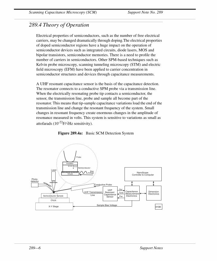
A UHF resonant capacitance sensor is the basis of the capacitance detection. The resonator connects to a conductive SPM probe via a transmission line. When the electrically resonating probe tip contacts a semiconductor, the sensor, the transmission line, probe and sample all become part of the resonator. This means that tip-sample capacitance variations load the end of the transmission line and change the resonant frequency of the system. Small changes in resonant frequency create enormous changes in the amplitude of resonance measured in volts. This system is sensitive to variations as small as
attofarads (10-22F/√Hz sensitivity).
Figure 289.4a: Basic SCM Detection System
NanoScopeController & Computer
UHFResonant
CapacitanceSensor
CapacitanceMeasurementElectronics
DimensionElectronics
Conductive Probe
Chuck
X-Y Stage Sample Bias Voltage
UHF TransmissionOut
Tune
PwrLine
Laser
Photo-detector
Semiconductor Sample
Chuck
Semiconductor
BiasVoltage
Probe
Insulatore e e
3108
289—6 Support Notes
Support Note No.289 Scanning Capacitance Microscopy (SCM)
Theory of Operation continued...
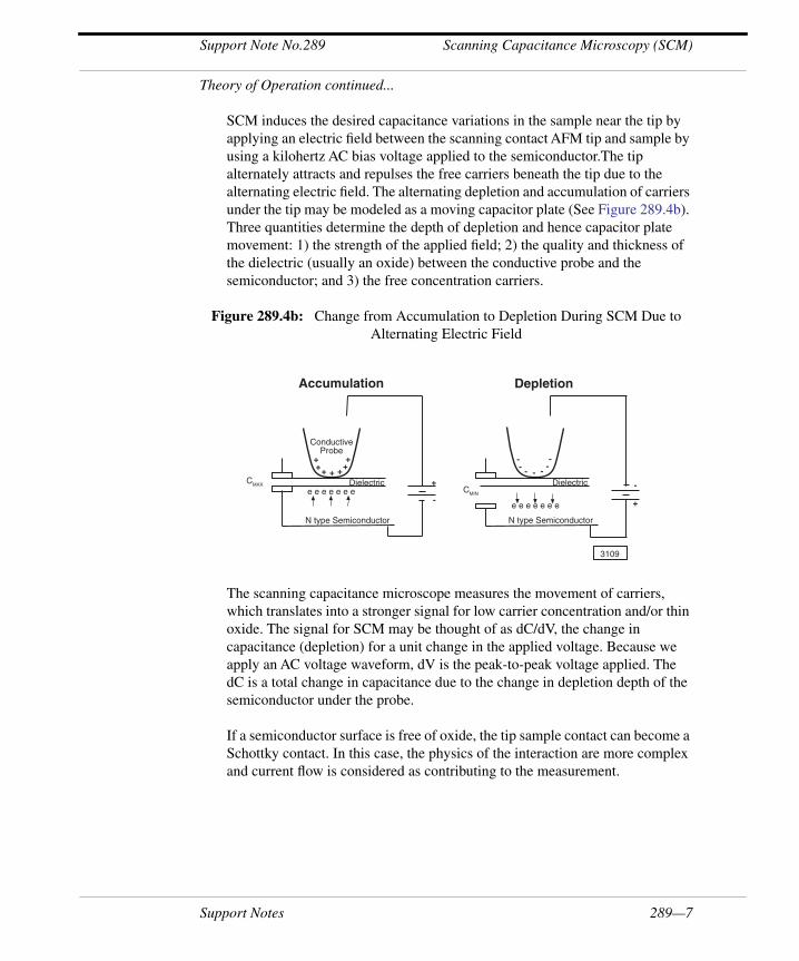
SCM induces the desired capacitance variations in the sample near the tip by applying an electric field between the scanning contact AFM tip and sample by using a kilohertz AC bias voltage applied to the semiconductor.The tip alternately attracts and repulses the free carriers beneath the tip due to the alternating electric field. The alternating depletion and accumulation of carriers under the tip may be modeled as a moving capacitor plate (See Figure 289.4b). Three quantities determine the depth of depletion and hence capacitor plate movement: 1) the strength of the applied field; 2) the quality and thickness of the dielectric (usually an oxide) between the conductive probe and the semiconductor; and 3) the free concentration carriers.
Figure 289.4b: Change from Accumulation to Depletion During SCM Due to Alternating Electric Field
The scanning capacitance microscope measures the movement of carriers, which translates into a stronger signal for low carrier concentration and/or thin oxide. The signal for SCM may be thought of as dC/dV, the change in capacitance (depletion) for a unit change in the applied voltage. Because we apply an AC voltage waveform, dV is the peak-to-peak voltage applied. The dC is a total change in capacitance due to the change in depletion depth of the semiconductor under the probe.
If a semiconductor surface is free of oxide, the tip sample contact can become a Schottky contact. In this case, the physics of the interaction are more complex and current flow is considered as contributing to the measurement.
-- - - - -
-
+
-Dielectric
e e e e e e e
CMIN
N type Semiconductor
Depletion
+++ + ++
+
+
-
ConductiveProbe
Dielectrice e e e e e e
CMAX
N type Semiconductor
Accumulation
3109
Support Notes 289—7
Scanning Capacitance Microscopy (SCM) Support Note No. 289
Theory of Operation continued...
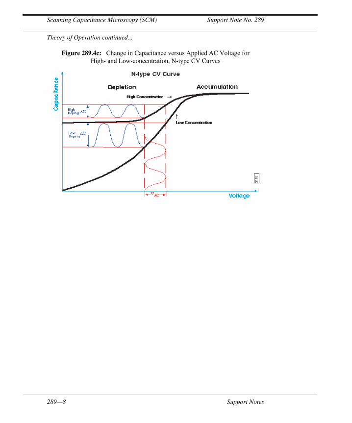
Figure 289.4c: Change in Capacitance versus Applied AC Voltage forHigh- and Low-concentration, N-type CV Curves
3110
289—8 Support Notes
Support Note No.289 Scanning Capacitance Microscopy (SCM)
Theory of Operation continued...
289.4.1 Capacitance-Voltage Relationship in Semiconductors
Capacitance-voltage has been used for more than 35 years to measure important material characteristics in semiconductors. Figure 289.4c shows a typical high frequency capacitance-verses-voltage (CV) relationship for high and low concentration N-type material. For P-type material, the CV curve’s polarity inverts. At positive voltages applied to the gate (or in our case a conductive probe) the carriers in the material (electrons for N-type) attract to the surface and accumulate there. In accumulation, the capacitor plates for the semiconductor are very close together and the total capacitance of the system is the capacitance of the dielectric. As the voltage on the gate swings negative, the electrons move away from the gate depleting the material of carriers. This increases the spacing between the semiconductor capacitor plates and lowers the capacitance. The lower concentration material depletes faster and hence the capacitance decreases faster with voltage. Therefore, the slope of the CV curve (or dC/dV) is larger for the low concentration. The SCM is a slope detector of the CV relationship.
The relationship between capacitance and voltage for a semiconductor is typically plotted on a C-V curve as shown in Figure 289.4c. For SCM imaging, apply a constant amplitude sine wave voltage to the sample (dV). This constructs an image of the amplitude of the capacitance modulation (dC). Adjust the DC bias to the sample, thereby moving the point around which the AC bias applies.
289.4.2 Closed Loop Feedback (Constant Depletion SCM)
Apply a feedback loop to the dC/dV curve. The amplitude of the applied AC voltage (dV) varies, while the feedback loop maintains a constant amplitude of modulation in the capacitance signal (dC). This constructs an image showing the voltage amplitude (dV) required to maintain the chosen dC modulation. The intent of this mode of operation is to scan across the sample with a constant depletion depth.
Support Notes 289—9

Scanning Capacitance Microscopy (SCM) Support Note No. 289
289.5 Installation/Setup of the SCM
Installation of the Dimension system for SCM differs from a standard Dimension system only in the installation of the SCM module on the AFM scanner head. For other installation issues, see your Dimension manual.
289.5.1 Installation of the SCM Module
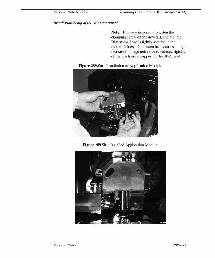
1. Remove the head by completing the following:
a. Unplug the Dimension head’s 21-pin connector.
b. Retract the clamping screw on the right hand side of the dovetail mount by turning it clockwise.
c. Gently remove the head.
2. Place the SCM sensor flush on the flat part of the piezo guard, and tighten it down using the two #2-56 screws. Be careful not to overtighten (See Figure 289.5a and Figure 289.5b).
Note: The screws and a matching screwdriver are included in the application module kit.
3. Install the Dimension head on the dovetail mount by completing the following (See Figure 289.5a):
a. Tighten the clamping screw by turning it counter-clockwise until the head is secure.
b. Plug the head’s 21-pin connector and the SCM module’s 15-pin connector into the receptacles on the front of the microscope’s electronics box.
WARNING: When installing the Dimension head, carefully check the clearance between the sample/ stage and the tip/ scanner to prevent the tip/ scanner from crashing into the sample/ stage. If it appears that the tip/ scanner may crash when fully inserted, remove the Dimension head completely and execute the Motor/ Withdraw command. You may also select Stage/ Focus Surface and use the trackball to obtain sufficient clearance and avoid a crash.
289—10 Support Notes
Support Note No.289 Scanning Capacitance Microscopy (SCM)
Installation/Setup of the SCM continued...
Note: It is very important to fasten the clamping screw on the dovetail, and that the Dimension head is tightly secured in the mount. A loose Dimension head causes a large increase in image noise due to reduced rigidity of the mechanical support of the SPM head.
Figure 289.5a: Installation of Application Module
Figure 289.5b: Installed Application Module
Support Notes 289—11
Scanning Capacitance Microscopy (SCM) Support Note No. 289
Installation/ Setup of the SCM continued...
289.5.2 Select Desired Microscope
Prior to engaging with the SCM, a user must first adjust the modes of the SCM software according to desired imaging. To ensure optimal imaging, complete the following steps:
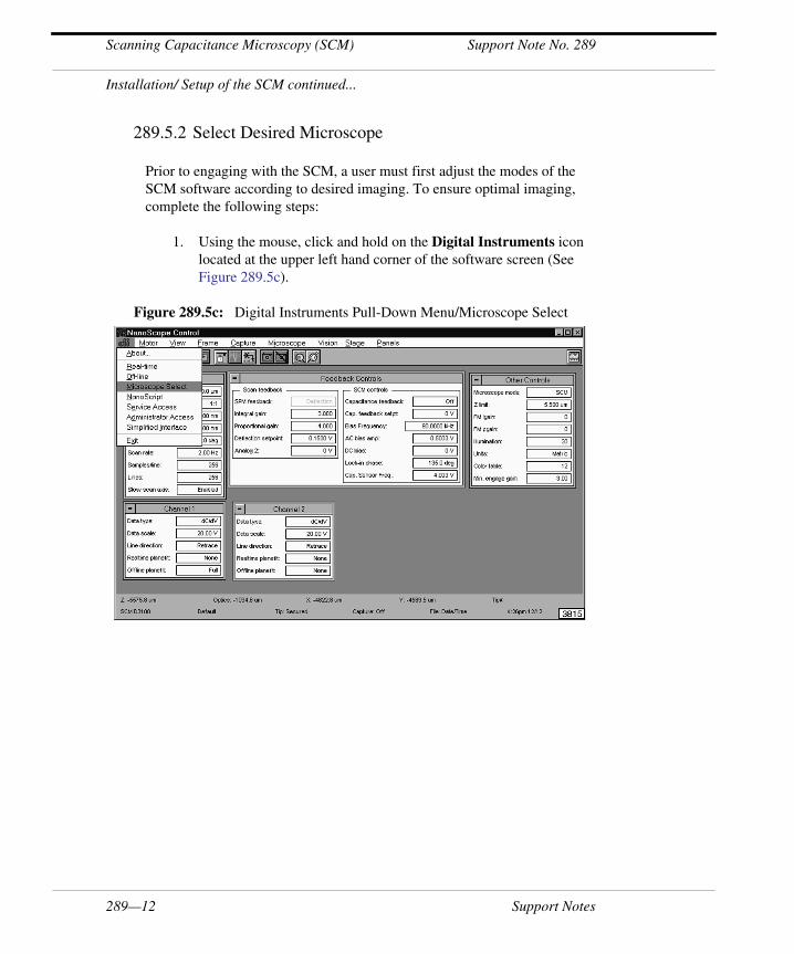
1. Using the mouse, click and hold on the Digital Instruments icon located at the upper left hand corner of the software screen (See Figure 289.5c).
Figure 289.5c: Digital Instruments Pull-Down Menu/Microscope Select
289—12 Support Notes

Support Note No.289 Scanning Capacitance Microscopy (SCM)
Installation/Setup of the SCM continued...
2. Double-click on Microscope Select to open the Microscope Select panel. Select the SCM D3100 option (See Figure 289.5d).
Figure 289.5d: Microscope Select Panel
Support Notes 289—13
Scanning Capacitance Microscopy (SCM) Support Note No. 289
Installation/Setup of the SCM continued...
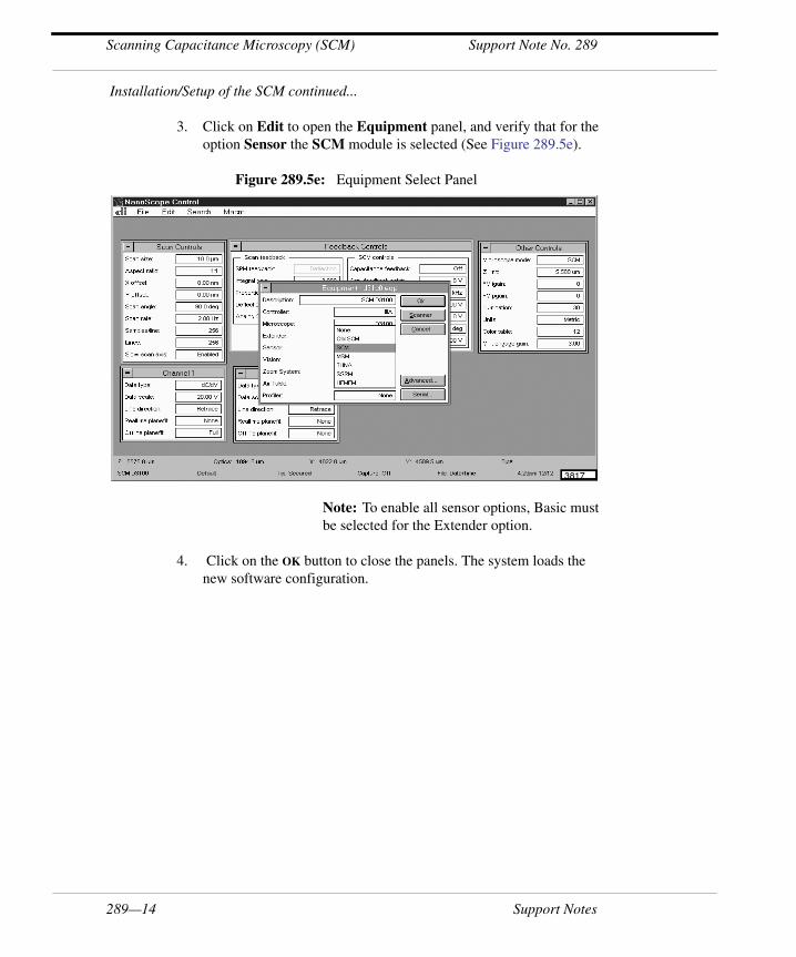
3. Click on Edit to open the Equipment panel, and verify that for the option Sensor the SCM module is selected (See Figure 289.5e).
Figure 289.5e: Equipment Select Panel
Note: To enable all sensor options, Basic must be selected for the Extender option.
4. Click on the OK button to close the panels. The system loads the new software configuration.
289—14 Support Notes

Support Note No.289 Scanning Capacitance Microscopy (SCM)
Installation/Setup of the SCM continued...
5. In the Other Controls panel (See Figure 289.5f) select SCM.
Figure 289.5f: Other Controls Panel
Note: The Feedback Controls panel displays all SCM control parameters as shown in Figure 289.5g.
Figure 289.5g: Feedback Controls Panel
Support Notes 289—15
Scanning Capacitance Microscopy (SCM) Support Note No. 289
Installation/Setup of SCM continued...
289.5.3 SCM Controls Panel
You may perform SCM measurements in both open loop mode and closed loop mode. Table 289.5a gives an overview of the different parameters related to open loop and closed loop SCM imaging.
Note: Deselect parameters from the panel by selecting the expansion key located in the top left hand corner of the Feedback Control panel. A pop-down menu appears allowing the user to select or deselect the different parameters.
Table 289.5a: SCM Control Parameters
Capacitance Feedback Turns closed loop SCM mode on or off.
Cap. Feedback SetpointSelects the dC/dV setpoint for closed loop
mode. Not used in open loop mode.
Bias FrequencyFrequency of the AC bias applied to chuck/
sample
AC Bias Ampl. Selectable AC bias to chuck/sample
DC Bias Ampl. Selectable DC bias to chuck/sample
Lock-In PhaseSelects the phase at which the SCM lock-in is
operated
Cap. Sensor Freq. Selects the capacitance sensor tuning voltage
289—16 Support Notes
Support Note No.289 Scanning Capacitance Microscopy (SCM)
289.6 SCM Imaging/Collecting Data
289.6.1 Sample Mounting
When we use the sample chuck in SCM to apply the DC and AC bias to the sample, the sample must make good electrical contact to the sample chuck. Electrically connect the sample by mounting it to a standard sample disk or stage using conducting epoxy or silver paint. Ensure the connection is good; a poor connection introduces noise and results in voltage loss. Specific instructions for preparing a cross-section surface are given in Section 289.8.
289.6.2 Tip Mounting
Selection
SCM uses an electrically conductive tip. Standard SCM tips include PtIr-coated tips and CoCr coated Si tips (MESP). Alternative tips are diamond coated tips (DCT-ESP) or uncoated Si tips (TESP). It is also possible to deposit custom coatings on standard Si cantilevers. In this case, make sure that any deposited metal you use adheres strongly to the Si cantilever. When selecting a tip for SCM, always bear in mind that SCM operates in the contact mode.
Mounting
The tip may be mounted as described in Chapter 5 of your SPM’s Instruction Manual. After mounting the tip onto the cantilever holder, plug the cantilever holder wire into the SCM sensor. Gently use your fingers or a pair of tweezers for this operation.
Note: Assure that the probe does not move or fall out of the spring clip holder. Be careful not to move the clip too far up so that it touches the sample prior to the tip upon engaging.
Support Notes 289—17
Scanning Capacitance Microscopy (SCM) Support Note No. 289
SCM Imaging/Collecting Data continued...
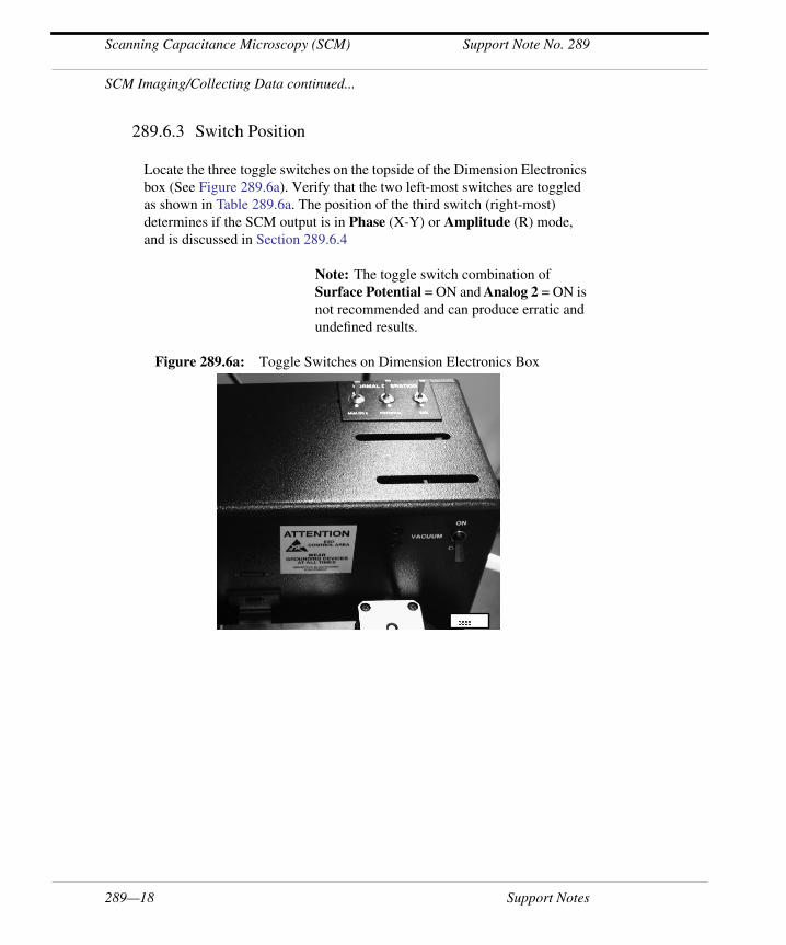
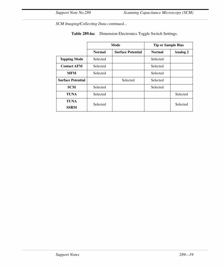
289.6.3 Switch Position
Locate the three toggle switches on the topside of the Dimension Electronics box (See Figure 289.6a). Verify that the two left-most switches are toggled as shown in Table 289.6a. The position of the third switch (right-most) determines if the SCM output is in Phase (X-Y) or Amplitude (R) mode, and is discussed in Section 289.6.4
Note: The toggle switch combination of Surface Potential = ON and Analog 2 = ON is not recommended and can produce erratic and undefined results.
Figure 289.6a: Toggle Switches on Dimension Electronics Box
289—18 Support Notes
Support Note No.289 Scanning Capacitance Microscopy (SCM)
SCM Imaging/Collecting Data continued...
Table 289.6a: Dimension Electronics Toggle Switch Settings.
Mode Tip or Sample Bias
Normal Surface Potential Normal Analog 2
Tapping Mode Selected Selected
Contact AFM Selected Selected
MFM Selected Selected
Surface Potential Selected Selected
SCM Selected Selected
TUNA Selected Selected
TUNA
SSRMSelected Selected
Support Notes 289—19
Scanning Capacitance Microscopy (SCM) Support Note No. 289
SCM Imaging/Collecting Data continued...
289.6.4 Imaging in Open Loop (dC/dV)
1. If you are not already operating in Real-time mode, select DI/ Real-time.
2. In the Other Controls panel, select SCM as the Microscope mode.
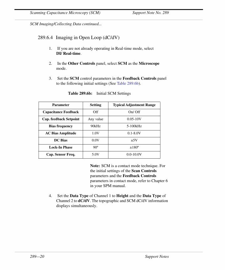
3. Set the SCM control parameters in the Feedback Controls panel to the following initial settings (See Table 289.6b).
Table 289.6b: Initial SCM Settings
Note: SCM is a contact mode technique. For the initial settings of the Scan Controls parameters and the Feedback Controls parameters in contact mode, refer to Chapter 6 in your SPM manual.
4. Set the Data Type of Channel 1 to Height and the Data Type of Channel 2 to dC/dV. The topographic and SCM dC/dV information displays simultaneously.
Parameter Setting Typical Adjustment Range
Capacitance Feedback Off On/ Off
Cap. feedback Setpoint Any value 0.05-10V
Bias frequency 90kHz 5-100kHz
AC Bias Amplitude 1.0V 0.1-8.0V
DC Bias 0.0V ±5V
Lock-In Phase 90º ±180º
Cap. Sensor Freq. 5.0V 0.0-10.0V
289—20 Support Notes
Support Note No.289 Scanning Capacitance Microscopy (SCM)
SCM Imaging/Collecting Data continued...
5. Once the parameters are set, click on the ENGAGE command and start the measurement.
Note: It will probably be necessary to make adjustments to a number of parameters (Integral Gain, Proportional Gain, Deflection Setpoint, etc.) before the image is optimized.
6. To minimize wear of the tip and sample decrease the contact forces between the tip and the sample as much as possible. This may be completed in one of the following ways:
a. Obtain a force plot and adjust the setpoint to a level just above the pull-off value, thus minimizing the force (See Chapter 11 of your SPM Manual).
b. Click on the Scope Mode command and observe the Height trace while reducing the setpoint. This reduces the force applied to the sample until the tip eventually lifts off the sample surface. You may go back to contact by slightly increasing the setpoint until you obtain a focused image.
7. While scanning, it will probably be necessary to make adjustments to a number of parameters in the Feedback Controls panel before the SCM image is optimized. Adjust parameters within the ranges shown in Table 289.6b. As parameters are adjusted, differences in the image become more apparent, leading to a better understanding of SCM. Tune some of the parameters, in particular the Cap. Sensor Frequency and the Lock-In Phase, using the sweeping features presented in Section 289.7.1.
Support Notes 289—21
Scanning Capacitance Microscopy (SCM) Support Note No. 289
SCM Imaging/Collecting Data continued...
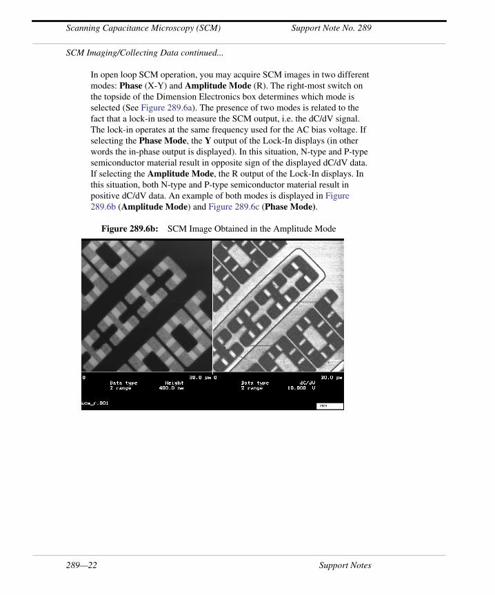
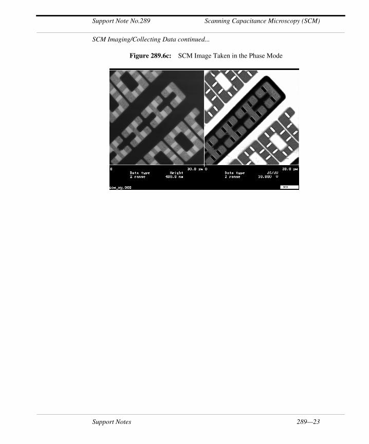
In open loop SCM operation, you may acquire SCM images in two different modes: Phase (X-Y) and Amplitude Mode (R). The right-most switch on the topside of the Dimension Electronics box determines which mode is selected (See Figure 289.6a). The presence of two modes is related to the fact that a lock-in used to measure the SCM output, i.e. the dC/dV signal. The lock-in operates at the same frequency used for the AC bias voltage. If selecting the Phase Mode, the Y output of the Lock-In displays (in other words the in-phase output is displayed). In this situation, N-type and P-type semiconductor material result in opposite sign of the displayed dC/dV data. If selecting the Amplitude Mode, the R output of the Lock-In displays. In this situation, both N-type and P-type semiconductor material result in positive dC/dV data. An example of both modes is displayed in Figure 289.6b (Amplitude Mode) and Figure 289.6c (Phase Mode).
Figure 289.6b: SCM Image Obtained in the Amplitude Mode
289—22 Support Notes
Support Note No.289 Scanning Capacitance Microscopy (SCM)
SCM Imaging/Collecting Data continued...
Figure 289.6c: SCM Image Taken in the Phase Mode
Support Notes 289—23
Scanning Capacitance Microscopy (SCM) Support Note No. 289
SCM Procedure for Imaging/ Collecting Data continued...
289.6.5 Imaging In Closed Loop
1. Complete 1 -7 of Section 289.6.4 to obtain a good SCM image in Open Loop mode.
2. Switch the right-most switch on the Dimension Electronics box into the Amplitude (R) position (See Figure 289.6a).
3. Set the Data Type of Channel 2 to Feedback Bias.
4. Switch the Cap. Feedback in the SCM Control parameters On. Set the Cap. Feedback Setpoint to the initial value of 0.2 V.
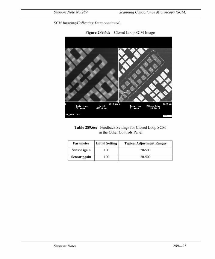
5. The proportional and integral gain of the capacitance feedback loop are in the Other Controls panel. Adjust the gains, in combination with the Cap. Feedback Setpoint, as indicated in Table 289.6c to improve the image quality. Depending upon the sample’s capacitance properties, optimize the image within the range of values shown in Table 289.6b and Table 289.6c.
Note: An example of closed loop SCM operation is shown in Figure 289.6c. The lowly doped areas result in a low signal, while the highly doped areas result in a high signal. In closed loop mode, N-type and P-type semiconductor material result in the same polarity of output signal.
289—24 Support Notes
Support Note No.289 Scanning Capacitance Microscopy (SCM)
SCM Imaging/Collecting Data continued...
Figure 289.6d: Closed Loop SCM Image
Table 289.6c: Feedback Settings for Closed Loop SCM in the Other Controls Panel
Parameter Initial Setting Typical Adjustment Ranges
Sensor igain 100 20-500
Sensor pgain 100 20-500
Support Notes 289—25
Scanning Capacitance Microscopy (SCM) Support Note No. 289
289.7 Sweeping
The NanoScope software permits the user to sweep or ramp various signals in a specific location. Typically we place the SCM tip at the center of the image, where the ramping curve performs and captures. By applying an X or Y offset you may move the tip to other locations.
There are two ways of performing sweeps or ramps of various signals in SCM: the Sweep Generic command, and the Force Curve command (See Section 289.7.1 and Section 289.7.3).
289.7.1 Sweeping Using the Sweep Generic Command
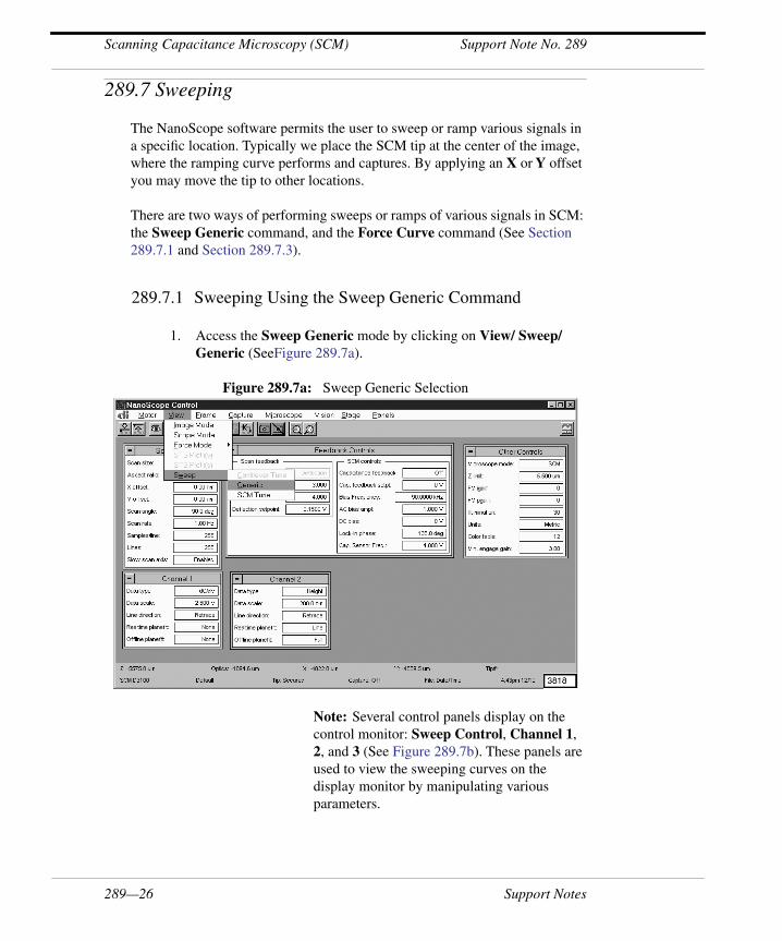
1. Access the Sweep Generic mode by clicking on View/ Sweep/ Generic (SeeFigure 289.7a).
Figure 289.7a: Sweep Generic Selection
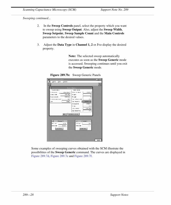
Note: Several control panels display on the control monitor: Sweep Control, Channel 1, 2, and 3 (See Figure 289.7b). These panels are used to view the sweeping curves on the display monitor by manipulating various parameters.
289—26 Support Notes

Support Note No.289 Scanning Capacitance Microscopy (SCM)
Sweeping continued...
Note: The Sweep Control panel displays a number of Graph Control parameters and the standard set of Main Control parameters (including the standard feedback parameters and the SCM control parameters). The Graph Control parameters are summarized in Table 289.7a.
Table 289.7a: Graph Control Parameters in the Sweep Generic Mode
Sweep Output
Selects the property which is being swept. The properties shown depend on the selected microscope mode (SCM, SSRM, etc.). In SCM the following properties may be swept: Cap. Feedback Set-point, Bias frequency, AC Bias Amplitude, DC Bias Lock-In
Phase, Cap. Sensor Frequency.
Sweep Width Selects the range of the sweeping.
Sweep Setpoint Sets the midpoint of the sweep.
Sweep Sample Count
Selects the number of data points used during one sweep.
Units May be switched from Metric to Volts.
Support Notes 289—27
Scanning Capacitance Microscopy (SCM) Support Note No. 289
Sweeping continued...
2. In the Sweep Controls panel, select the property which you want to sweep using Sweep Output. Also, adjust the Sweep Width, Sweep Setpoint, Sweep Sample Count and the Main Controls parameters to the desired values.
3. Adjust the Data Type in Channel 1, 2 or 3 to display the desired property.
Note: The selected sweep automatically executes as soon as the Sweep Generic mode is accessed. Sweeping continues until you exit the Sweep Generic mode.
Figure 289.7b: Sweep Generic Panels
Some examples of sweeping curves obtained with the SCM illustrate the possibilities of the Sweep Generic command. The curves are displayed in Figure 289.7d, Figure 289.7e and Figure 289.7f.
289—28 Support Notes
Support Note No.289 Scanning Capacitance Microscopy (SCM)
Sweeping continued...
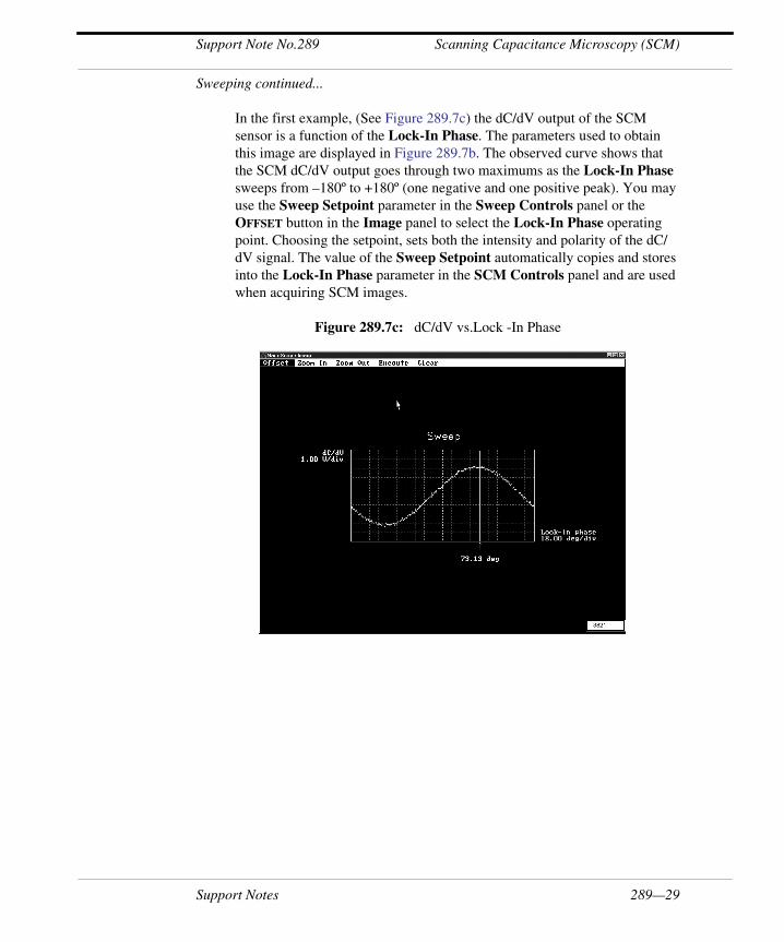
In the first example, (See Figure 289.7c) the dC/dV output of the SCM sensor is a function of the Lock-In Phase. The parameters used to obtain this image are displayed in Figure 289.7b. The observed curve shows that the SCM dC/dV output goes through two maximums as the Lock-In Phase sweeps from –180º to +180º (one negative and one positive peak). You may use the Sweep Setpoint parameter in the Sweep Controls panel or the OFFSET button in the Image panel to select the Lock-In Phase operating point. Choosing the setpoint, sets both the intensity and polarity of the dC/dV signal. The value of the Sweep Setpoint automatically copies and stores into the Lock-In Phase parameter in the SCM Controls panel and are used when acquiring SCM images.
Figure 289.7c: dC/dV vs.Lock -In Phase
Support Notes 289—29
Scanning Capacitance Microscopy (SCM) Support Note No. 289
Sweeping continued...
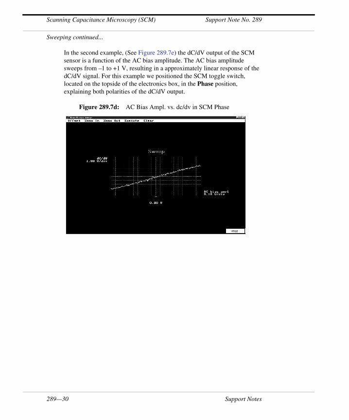
In the second example, (See Figure 289.7e) the dC/dV output of the SCM sensor is a function of the AC bias amplitude. The AC bias amplitude sweeps from –1 to +1 V, resulting in a approximately linear response of the dC/dV signal. For this example we positioned the SCM toggle switch, located on the topside of the electronics box, in the Phase position, explaining both polarities of the dC/dV output.
Figure 289.7d: AC Bias Ampl. vs. dc/dv in SCM Phase
289—30 Support Notes
Support Note No.289 Scanning Capacitance Microscopy (SCM)
Sweeping continued...
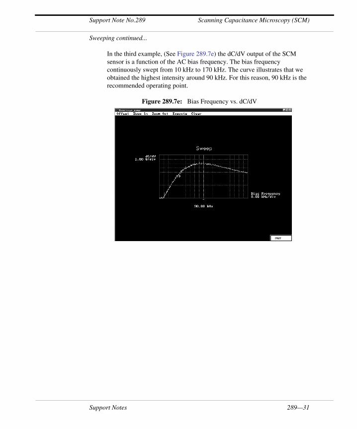
In the third example, (See Figure 289.7e) the dC/dV output of the SCM sensor is a function of the AC bias frequency. The bias frequency continuously swept from 10 kHz to 170 kHz. The curve illustrates that we obtained the highest intensity around 90 kHz. For this reason, 90 kHz is the recommended operating point.
Figure 289.7e: Bias Frequency vs. dC/dV
Support Notes 289—31
Scanning Capacitance Microscopy (SCM) Support Note No. 289
Sweeping continued...
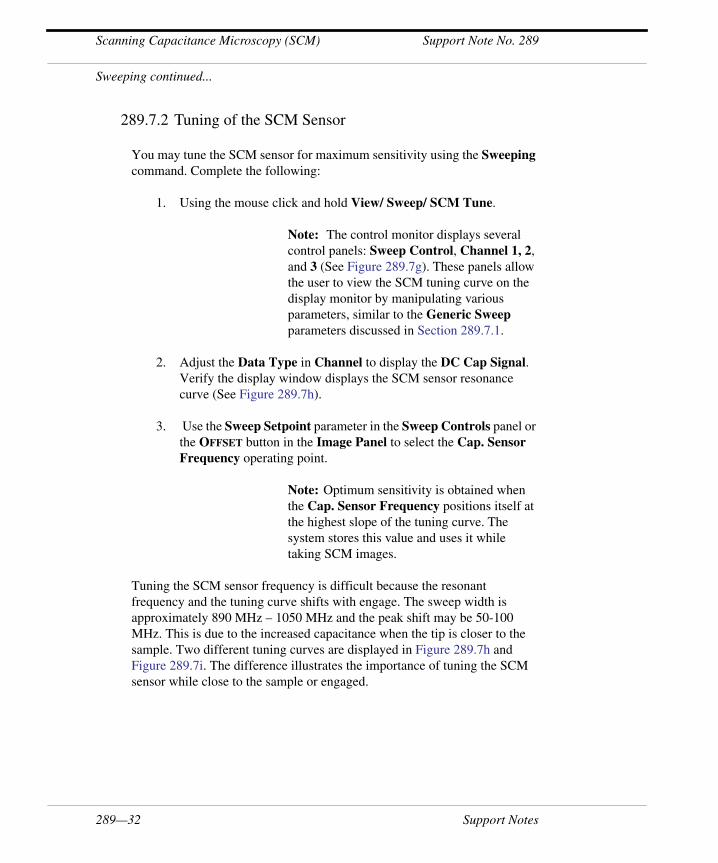
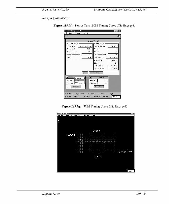
289.7.2 Tuning of the SCM Sensor
You may tune the SCM sensor for maximum sensitivity using the Sweeping command. Complete the following:
1. Using the mouse click and hold View/ Sweep/ SCM Tune.
Note: The control monitor displays several control panels: Sweep Control, Channel 1, 2, and 3 (See Figure 289.7g). These panels allow the user to view the SCM tuning curve on the display monitor by manipulating various parameters, similar to the Generic Sweep parameters discussed in Section 289.7.1.
2. Adjust the Data Type in Channel to display the DC Cap Signal. Verify the display window displays the SCM sensor resonance curve (See Figure 289.7h).
3. Use the Sweep Setpoint parameter in the Sweep Controls panel or the OFFSET button in the Image Panel to select the Cap. Sensor Frequency operating point.
Note: Optimum sensitivity is obtained when the Cap. Sensor Frequency positions itself at the highest slope of the tuning curve. The system stores this value and uses it while taking SCM images.
Tuning the SCM sensor frequency is difficult because the resonant frequency and the tuning curve shifts with engage. The sweep width is approximately 890 MHz – 1050 MHz and the peak shift may be 50-100 MHz. This is due to the increased capacitance when the tip is closer to the sample. Two different tuning curves are displayed in Figure 289.7h and Figure 289.7i. The difference illustrates the importance of tuning the SCM sensor while close to the sample or engaged.
289—32 Support Notes
Support Note No.289 Scanning Capacitance Microscopy (SCM)
Sweeping continued...
Figure 289.7f: Sensor Tune SCM Tuning Curve (Tip Engaged)
Figure 289.7g: SCM Tuning Curve (Tip Engaged)
Support Notes 289—33

Scanning Capacitance Microscopy (SCM) Support Note No. 289
Sweeping continued...
Figure 289.7h: SCM Tuning Curve (Tip Withdrawn)
289.7.3 Ramping Using Force Curve Command: dC/dV – V Spectra
The second method of performing ramps of various SCM signals uses the Force Curve command. A typical application is the measurement of dC/dV –V spectra.
1. Go to View/ Force Mode/ Calibrate.
Note: The command screen appears displaying the different ramping panels (See Figure 289.7j).You may use these panels to view the ramping curves on the display monitor by manipulating various parameters.
Note: The Main Controls panel shows a number of Ramp Control parameters and a set of Display parameters. The Ramp Control parameters are summarized in Table 289.7b, while the Display parameters are summarized in Table 289.7c.
289—34 Support Notes

Support Note No.289 Scanning Capacitance Microscopy (SCM)
Sweeping continued...
Table 289.7b: Ramp Control Parameters in the Main Controls Panel
Note: Scan Rate, Forward Velocity and Reverse Velocity are interdependent. Changing one of the velocities affects the overall scan rate of the others and vice versa.
Ramp Channel
Selects the property which is being ramped. The properties shown depend on the selected microscope mode (SCM, SSRM, etc.). In SCM the following properties may be
ramped: Z (for standard force curve measurements), DC Bias and Cap. Sensor Frequency.
Ramp Begin/ Ramp End
Defines the beginning and ending of a ramp.
Scan rateAll ramps are begin-end-begin cycles, and the scan rate
refers to one complete cycle.
Forward veloc-ity & Reverse
Velocity
Defines the ramp value from beginning to end, or end to beginning.
X and Y Offset Moves the tip to a different location.
Number of Samples
Determines the number of samples per ramp (minimum 16, maximum 64,000).
Average CountAllows several ramps to be averaged (minimum 1,
maximum 1024).
Support Notes 289—35

Scanning Capacitance Microscopy (SCM) Support Note No. 289
Sweeping continued...
Table 289.7c: Display Parameters in the Main Controls Panel
Figure 289.7i: Ramping Panels
2. In the Ramp Controls, select the property which you want to ramp using Ramp Channel.
3. Adjust the other parameters in the Ramp Controls and Display section of the Main Controls panel to the desired values (See Figure 289.7m).
Units Metric or Volts
Feedback Type
Ensures that the deflection feedback is ON during ramping.
Ramp- Enables feedback after each ramp cycle (start-end- feedback).
Cycle- Enables feedback after each ramp cycle (start-end-start-feedback).
Pixel- Enables feedback after every sample point of the ramp. This might be useful for extremely
slow ramps with few sample points.
Feedback Counts Select 50 for proper feedback.
Feedback Value Select to 0V
289—36 Support Notes
Support Note No.289 Scanning Capacitance Microscopy (SCM)
Sweeping continued...
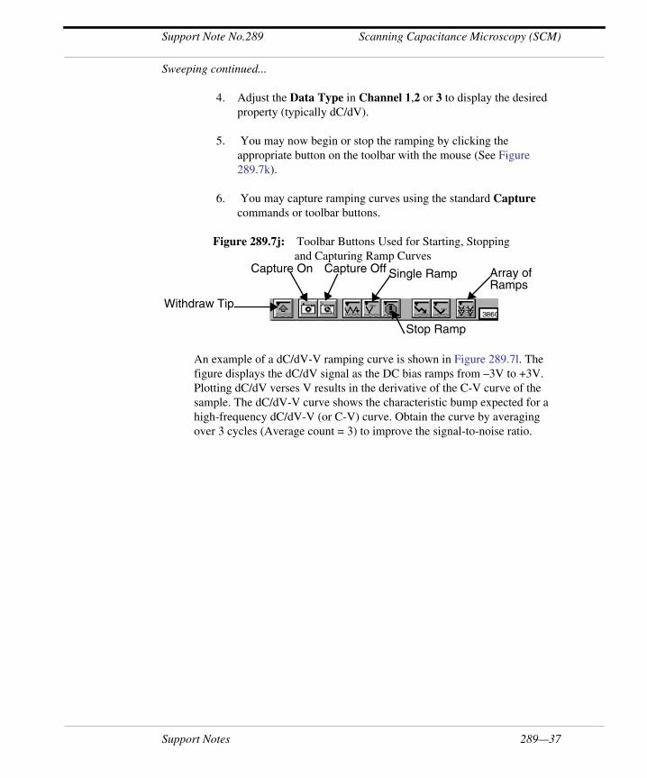
4. Adjust the Data Type in Channel 1,2 or 3 to display the desired property (typically dC/dV).
5. You may now begin or stop the ramping by clicking the appropriate button on the toolbar with the mouse (See Figure 289.7k).
6. You may capture ramping curves using the standard Capture commands or toolbar buttons.
Figure 289.7j: Toolbar Buttons Used for Starting, Stopping and Capturing Ramp Curves
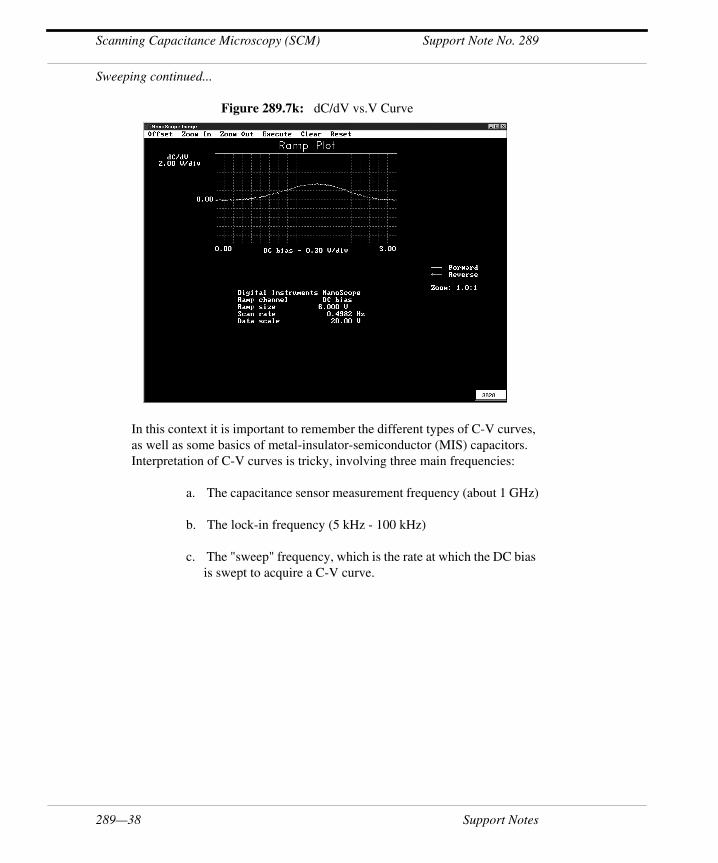
An example of a dC/dV-V ramping curve is shown in Figure 289.7l. The figure displays the dC/dV signal as the DC bias ramps from –3V to +3V. Plotting dC/dV verses V results in the derivative of the C-V curve of the sample. The dC/dV-V curve shows the characteristic bump expected for a high-frequency dC/dV-V (or C-V) curve. Obtain the curve by averaging over 3 cycles (Average count = 3) to improve the signal-to-noise ratio.
Withdraw Tip
Capture On Capture Off Single Ramp
Stop Ramp
Array ofRamps
Support Notes 289—37
Scanning Capacitance Microscopy (SCM) Support Note No. 289
Sweeping continued...
Figure 289.7k: dC/dV vs.V Curve
In this context it is important to remember the different types of C-V curves, as well as some basics of metal-insulator-semiconductor (MIS) capacitors. Interpretation of C-V curves is tricky, involving three main frequencies:
a. The capacitance sensor measurement frequency (about 1 GHz)
b. The lock-in frequency (5 kHz - 100 kHz)
c. The "sweep" frequency, which is the rate at which the DC bias is swept to acquire a C-V curve.
289—38 Support Notes
Support Note No.289 Scanning Capacitance Microscopy (SCM)
Sweeping continued...
In general, a signal is termed high-frequency (or low-frequency) if its period is shorter (or longer) than the delay time associated with the generation of minority carriers, e.g., to fill an inversion layer. There are three relevant type of C-V curves:
Low-frequency C-V curves
All frequencies (a,b,c) are slow enough that minority-carrier generation can bring the carrier distribution to the long-time configuration, i.e., all three frequencies are low. In a low-frequency C-V curve, the capacitance in the inversion region is high, comparable to the accumulation capacitance. The capacitance in the inversion region is high because minority-carrier generation screens the potential variations across the buried depletion layer, effectively shorting it out as a resistor would so the equivalent circuit looks similar to the one for accumulation. Only the oxide capacitance is relevant. It is impossible to measure low-frequency C-V curves at room temperature using the SCM since the minority-carrier generation rate is too low to modify the inversion layer population in 1 ns.
High-frequency C-V curves
Here the excitation frequency (a) is high; and therefore minority carriers cannot screen the buried depletion layer. The other frequencies (b, c) should be low so that the inversion layer has time to develop as the tip-sample potential is changed. If (b) is not low, the slope measured is not appropriate to this type of curve, since the inversion layer population is not able to follow the lock-in dither voltage. SCM data generally corresponds to high-frequency C-V curves.
Support Notes 289—39

Scanning Capacitance Microscopy (SCM) Support Note No. 289
Sweeping continued...
Deep-depletion C-V curves
In this case all three frequencies are high, so the inversion layer population goes unchanged by minority-carrier generation. In this case, potentials at all three frequencies can drop across the depletion layer, therefore: (1) the depletion-layer capacitance (in series with the oxide capacitance) is sensed in the inversion region; (2) the measured C-V- curve slope dC/dV appropriately reflects the changing depletion-layer width with sweep voltage; (3) the sweep voltage modulates the depletion-layer width so the bottom edge moves deeper, sampling different doped regions. This is the origin of the pulsed C-V measurements used for device characterization which are used to infer the depth profile of dopants in a fabricated MOS capacitor.
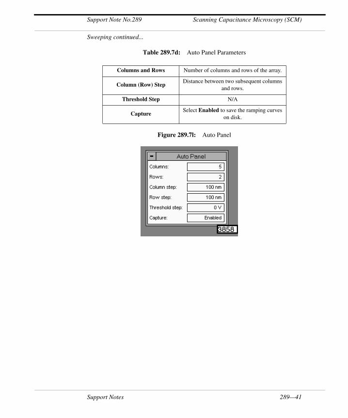
The ramping software also has some extra features useful for specific experiments. Using the Auto Panel (See Figure 289.7m) you can perform ramps in an array of points on the sample surface. The probe moves from one position to the next, while the force-feedback is maintained. In each point of the array, a ramp is executed and captured. For each ramping curve the system uses the same set of control parameters. Table 289.7d gives an overview of the different parameters associated to this operation.
289—40 Support Notes
Support Note No.289 Scanning Capacitance Microscopy (SCM)
Sweeping continued...
Table 289.7d: Auto Panel Parameters
Figure 289.7l: Auto Panel
Columns and Rows Number of columns and rows of the array.
Column (Row) StepDistance between two subsequent columns
and rows.
Threshold Step N/A
CaptureSelect Enabled to save the ramping curves
on disk.
Support Notes 289—41

Scanning Capacitance Microscopy (SCM) Support Note No. 289
Sweeping continued...
A second set of parameters allows for a more detailed control of the ramping curves. This set of parameters is in the Scan Mode panel (See Figure 289.7m). Table 289.7e displays the different parameters and their function. The features include the possibility to limit the output signal (dC/dV in SCM) to user-defined values by using the Trigger Mode. The Scan Mode panel also offers two parameters which may be used to independently delay times at the end of the start-end ramp, or at the end of a complete start-end-start cycle. The Scan Mode panel also displays a number of parameters which are only related to the measurement of force curves (Start mode, End mode, Z step size, Auto Offset). These parameters are described in Chapter 11 – Force Imaging of your SPM Instruction Manual.
Figure 289.7m: Scan Mode Panel
Table 289.7e: Scan Mode Parameters
Trigger ModeThis turns the Trigger Mode on and off. For dC/dV-V
curves select Absolute tomturn the trigger on.
Trigger ChannelFor dC/dV-V curves select dC/dV for triggering of
the capacitance signal.
Trigger Threshold This sets the trigger value.
Trigger Direction Select between negative and positive slope.
Ramp Delay This adds a delay time following each start-end ramp.
Reverse DelayThis adds a delay time following each complete start-
end-start cycle.
289—42 Support Notes
Support Note No.289 Scanning Capacitance Microscopy (SCM)
289.8 Sample Preparation for SCM
For 2-D carrier profiling the region of interest (often subsurface) must be accessible to the profiling instrument. Therefore, a cross-section through the sample to expose this region is required. Cross-section preparation of semiconductors usually involves cleaving and/or polishing. The most important criteria for the cross-sectional surface are: low roughness, no surface damage and cleanliness. This section provides a quick overview of possible sample preparation techniques, which the microscopist may employ using a diamond saw, a lapper and some silver epoxy. A sputtering chamber is often required. In general, standard electron microscopy techniques for sample preparation work well for SCM, however, the surface finish required is more exacting. The following technique may be carried out and a sample prepared within a few hours with a little practice.
289.8.1 Equipment and Supplies
Capital Sample Preparation Equipment
• N2 Dry Box
• Hot Plate
• Nikon Optihot-100 with 10 or 20X wide field eye pieces
• 5,20 and 50X Brightfield/ Darkfield/ Differential Interference Contrast (BD, DIC plan Apo) objectives
• 100 or 150X plan Apo BD objective
• Stereo zoom scope (Nikon SMZ-2 + ringlight and stand)
• Buehler ecomet 3 or 4 polisher
• UV Light source (Thorlabs phone number 201-579-7227, mode; l number UV 75)
Support Notes 289—43
Scanning Capacitance Microscopy (SCM) Support Note No. 289
Sample Preparation for SCM continued...
Consumables
• X section holder (Allied Hightech PN 69-30000)
• Glass slides
• Epoxy (Epoxy bond 110 Allied PN 71-10000)
• Silver epoxy (Dynaloy PN 325 A/B Hanover, NJ)
• Silver paint (Ted Pella #16035)
• Replication tape (Ted Pella #44841)
• Diamond Lapping Films: 0.1, 0.5, 1, 6 and 15m Buehler PN 15-7691,6795,6801,6807,6815
• Diamond suspensions for Texmet 0.1,0.25 m Buehler PN 40-6528,6529
• Texmet 1000 polish pad Buehler PN 40-7618
289.8.2 Cross Section Sample Preparation
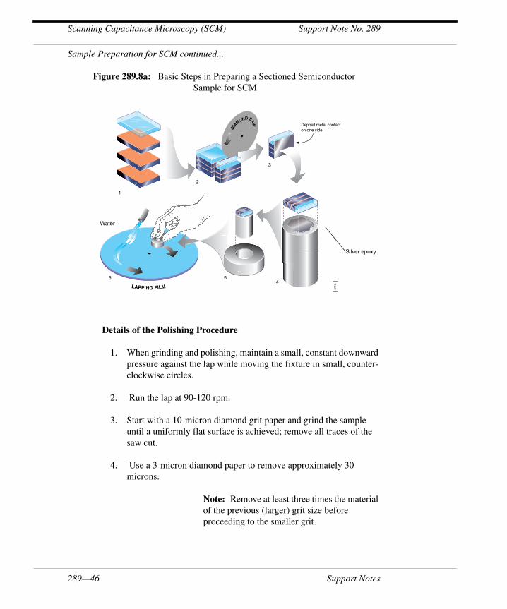
The different steps in the cross section preparation used for SCM are schematically represented in Figure 289.8a. The principal steps are as follows:
1. Cement the semiconductors into a stacked “sandwich” using G1 epoxy or equivalent.
a. Press the pieces together to remove all air bubbles.
b. Epoxy the glass plates can be epoxied to the bottom and top of the sandwich to protect the semiconductors within and provide strength.
c. Allow the epoxied stack to heat cure thoroughly.
2. Use a diamond saw to remove a slice of the semiconductor sandwich approximately 0.5 mm thick.
Sample Preparation for SCM continued...
289—44 Support Notes
Support Note No.289 Scanning Capacitance Microscopy (SCM)
3. To ensure optimal electrical contact, sputter the semiconductor stack with gold on its underside where it will contact the puck and/or stage of the microscope.
Note: It is best to leave this side unpolished before sputtering.
4. Using the silver epoxy or a low temperature wax, attach the coated side of the sample to the underside of a polishing fixture. Spread the coating evenly to leave a broad contact area.
5. In turn, insert the fixture into a separate ring to keep the ring perpendicular to the lap.
Note: Other equivalent fixtures are available from different polishing equipment suppliers.
6. Polish the top (imaging) side of the semiconductor sandwich. Verify that the sample is ground and polished flat to an RMS roughness of < 0.2 nm to produce a superior image.
7. Complete UV treatment and cleaning. The insulating properties of the silicon oxide film improves by UV irradiation.
a. Place the sample on a hot plate at about 200-300ºC for 20 minutes of which 1 minute of high-intensity UV irradiation. A UV light source from Torr labs can be used for this purpose.
Note: This preparation step results in a surface which shows no Fermi-level pinning and only a moderate density of surface electronic states.
Support Notes 289—45
Scanning Capacitance Microscopy (SCM) Support Note No. 289
Sample Preparation for SCM continued...
Figure 289.8a: Basic Steps in Preparing a Sectioned Semiconductor Sample for SCM
Details of the Polishing Procedure
1. When grinding and polishing, maintain a small, constant downward pressure against the lap while moving the fixture in small, counter-clockwise circles.
2. Run the lap at 90-120 rpm.
3. Start with a 10-micron diamond grit paper and grind the sample until a uniformly flat surface is achieved; remove all traces of the saw cut.
4. Use a 3-micron diamond paper to remove approximately 30 microns.
Note: Remove at least three times the material of the previous (larger) grit size before proceeding to the smaller grit.
LAPPING FILM
1
2
3
456
Deposit metal contacton one sideD
IA
MOND SAW
311
3
Silver epoxy
Water
289—46 Support Notes

Support Note No.289 Scanning Capacitance Microscopy (SCM)
Sample Preparation for SCM continued...
Diamond lapping films come in different sizes and are used to incrementally achieve a finer and finer grind. Generally, diamond paper is used in 5-minute sessions, proceeding in the following order:
• 10-micron: Use to remove saw marks and flatten sample.
• 3-micron: 5 min.
• 1-micron: 5 min.
• 0.5-micron: As needed.
• 0.1-micron: As needed.
5. Remove the surface damage left by the diamond paper process by using a colloidal diamond slurry. To avoid contamination, use a new polish pad dedicated to one grit (e.g., napless cloth). The following grinding order gives good results:
• 1-micron: 5 min.
• 0.5-micron: 10 min.
• 0.25-micron: 20 min.
• 0.1-micron: As needed.
• 0.05-micron: As needed.
6. Use 0.05-micron colloidal silica to do the final cleaning and polishing of the sample surface by applying for 15-30 seconds, followed by running clean water for at least 30 seconds.
7. Clean the sample surface with a swab and soapy running water, then wipe or blow dry.
Support Notes 289—47
Scanning Capacitance Microscopy (SCM) Support Note No. 289
Sample Preparation for SCM continued...
8. If a powered lap is unavailable, polish and grind the sample on a stationary flat lap by moving the fixture and ring in small figure-eight motions while periodically rotating the fixture within the ring to ensure even abrasion.
Note: Be certain to keep the fixture and lap wetted, and always clean completely before switching to a smaller grit.
Note: The most important tools in polishing are patience and a good optical microscope for inspection of the sample surface—e.g., bright field (BF), dark field (DF) and differential interference contrast (DIC) combined objectives in sizes of 5X, 20X and 50X.
9. When grinding and polishing are complete, clean the sample thoroughly using water and wipe or blow dry.
289—48 Support Notes
Support Note No.289 Scanning Capacitance Microscopy (SCM)
Sample Preparation for SCM continued...
289.8.3 Sample Cleaning Procedure
Just as topographic imaging can be adversely affected by contamination on the surface of the sample, an electrical measurement technique such as scanning capacitance can be fundamentally changed by the presence of water layers, ionic residue or charges trapped in the oxide. After time, the images obtained from samples may change relative to what was imaged in final tests at the factory. After failure modes such as broken tips and incorrect measurement parameters are ruled out, additional problem concern the samples themselves.
The SCM applies a local field between the tip and sample and measures the response of carriers to that field. Local charge may create fields which counteract the applied field, thus nulling the capacitive effect. This is seen in SCM as a loss of contrast or variation in the expected sample response. Due to the geometry of the tip / dielectric / silicon of the samples, a local packet of charge can produce a localized effect equivalent to many volts of applied field either pinning the carriers at the surface or depleting the surface of free carriers. Each of these charge effects destroy contrast in the SCM. It is necessary to remove this charge.
Another source of lost (and unrecoverable) contrast are trapped and mobile charges. These are charges in the dielectric material (in this case oxide). The trapped charge can be due to charge pumped into the oxide by applying a voltage sufficient to flow current (i.e., ± 8 V). Some of the charge (both positive and negative) may remain trapped and create local fields. Mobile charge refers to predominately sodium and potassium ions from contamination (usually from your fingers) which may diffuse into the oxide. These sources of charge are not removable and may only be avoided by reducing the amount of handling and voltage stress applied to the material. Regular cleaning and careful handling can mitigate further deterioration of the samples.
WARNING: Do not use your fingers. Only handle samples with clean tweezers. Preferable storage is in a sample box and inside a nitrogen or desiccated dry box. This is particularly true for humid climates. Much of the cleaning effect will provide a hydrophobic (water fearing) surface on the oxide. This effect lasts longer if the sample is kept dry.
Support Notes 289—49
Scanning Capacitance Microscopy (SCM) Support Note No. 289
Sample Preparation for SCM continued...
For cleaning, there are several preferred methods, used separately or in combination, to achieve the best results. You may find that one or the other works best. To complete the basic cleaning process:
Replicating Tape After UV Light Baking
Cover the sample with a spray of clean acetone and set a square of acetate replicating tape over the surface. Replicating tape, commonly used in electron microscopy, partially dissolves in the acetone and then dries and adheres tightly to the sample surface. When you peel the tape back, the tape holds on to whatever was on the surface of the sample. The tape may also be left on the sample as a protective coating.
CAUTION: Clean samples with solvents only in a well ventilated area. Dispose of all wipes and swabs properly.
The second method requires a bit more sophistication and treats the surface with a passivation associated with the alkali solution in a common chem-mechanical polishing compound.
Silica
1. Wipe the sample with either an acetone or alcohol to remove oils.
Next apply colloidal silica suspension1 to the sample surface and rub it around with a Q-tip.
2. Rinse this off with deionized water.
3. Use a few drops of soap2 and another Q-tip to clean the surface of the silica particles.
1. The Silica solution I use is from Allied Hi Tech products, Rancho Dominuez, CA. It is standard 0.05 um colloidal silica suspension, non-crystallizing (the blue stuff). Every shop that sells polish equipment and supplies will have an equivalent product.
2. Joy® soap seems to be the domestic product of choice if you don't have the micro clean variety from a scientific supply store.
289—50 Support Notes

Support Note No.289 Scanning Capacitance Microscopy (SCM)
Sample Preparation for SCM continued...
4. Rinse the sample again in deionized water and blow dry from one edge with clean filtered air or nitrogen.
Note: This method may be more effective against the charge layer on surface.
Support Notes 289—51

Scanning Capacitance Microscopy (SCM) Support Note No. 289
289.9 Troubleshooting
Problem: The microscope will not engage
Solution: Check that the spring clip or the wire on the cantilever holder does not touch the sample before the tip when trying to engage. If so, pull the clip back a bit.
Problem: No SCM signal is received
Solution: If no SCM signal is received, although you expect the sample to be suited for SCM measurements, check the following steps:
1. Are you using a metal coated tip? If not, replace your current tip with a metal coated tip.
2. Are you using an SCM cantilever holder, and is is the wire plugged in? If not, use a SCM cantilever holder, and assure that the wire is plugged in.
3. Have you selected the advised options in the Equipment Select menu? If not, adjust the parameters in the Equipment Select panel.
4. Are you applying an AC Bias? Is the DC Bias within the recommended range? If not, apply an AC Bias and adjust the range of your current DC Bias.
5. Is your sample appropriate for SCM? There are many possible problems here. Try a Digital Instruments, Veeco practice sample.
6. Is the sensor plugged in? If not, plug in the sensor.
7. Are the toggle switches on the topside of the electronics box in the advised position? If not, switch the toggle switches to the advised position.
289—52 Support Notes