Embed Size (px)
Citation preview

Drain Extended MOS DevOptim
Ankur Gupta1, Mayank ShrA. N. Chand
1CEN, EE Department, Indian Institute Indian Institute of Science Bangalore, Indi
Neubiberg, M
Abstract This paper explores drain extended MOS
design guidelines for an area scaled, ESD radio frequency power amplifier (RF PAsystem-on-chip applications in 28nm Simultaneous improvement of device-circand ESD robustness is discussed for the firsdesign optimization a 45% increase in gpower-added efficiency of RF PA at improvements in ESD robustness experimentally.
Introduction Advanced system-on-chip (SoC) concepts
all the functionalities on the same Si Diepower radio frequency power amplifiers (RFmanagement modules [1]-[2]. State-of-the-arPA is realized by discrete III-V deviceintegration of these device types on Si substTherefore, for CMOS based advanced Ssolution has to be explored. Drain e(DeNMOS) device is a potential candapplications in advance CMOS nodes [4]-[5for implementation of an integrated RF PA node CMOS is low breakdown voltage, seESD stress and nonlinear device characteridiscloses DeMOS device design guidelines integrated high performance RF PA with arobustness.
Experiments and ResulDeNMOS device (Fig. 1) was fabricated
technology node, using process and designfor low power devices. Total fabricated electdevice was 1.6mm. In order to study deviceRF PA application, the RF circuit was mboard. Schematic of the PA circuit is shownwith the biasing and matching networks. A cused at the DC supplies in order to de-cougenerated by the circuit from DC. Figphotograph of the fabricated PA circuit prloss laminate. Small signal s-parameter meconducted on die, to design the matching andfor the RF PA (Fig. 3). The DeNMOS dbiased slightly above the threshold voltage inthe PA in class-AB mode. Output power
vice Design for Integrated RF PA in 28mized FoM and ESD Robustness
rivastava2, Maryam Shojaei Baghini1, Dinesh K
dorkar1, Harald Gossner3 and V. Ramgopal Rao1
of Technology Bombay, India (email: [email protected] (email: [email protected]), 3Intel Corp., Platfo
Munich, Germany (email: [email protected])
(DeMOS) device robust integrated
A) for advanced node CMOS.
cuit performance st time. By device gain and 25% in
1GHz, and 5× are reported
push to integrate e including high F PA) and power rt high power RF s [3]. However, trate is not trivial. SoC, a Si based extended NMOS didate for such 5]. The challenge into a sub-65nm
ensitivity towards istics. This paper for designing an
an excellent ESD
lts in 28nm CMOS
n rules developed trical width of the e’s suitability for
mounted on a test n in Fig. 2a along capacitor ladder is uple the RF noise . 2b shows the repared on a low easurements were d biasing network
device’s gate was n order to operate r of the PA was
measured for a 50Ω load, as shownthe standard DeNMOS device off23.9dBm at 1-dB compressioncorresponds to a power density ofMeasured RF gain of the PA circuefficiency is 46% and power ad40.2% at 1-dB compression point. R
Fig. 1: Cross-sectional view of the DeNMCMOS node. Figure depicts a single finger sin a two finger configuration on silicon withfingers.
Fig. 2: (a) RF PA circuit, which is used aperformance of the advance CMOS node DeNthis work. (b) Board level implementation odesign and RF PA performance analysis. A l0.8mm (TanD = 0.0004), dielectric constan70µm was used for board level implementatdie to PCB were made using 25µm gold wiconductive epoxy for proper thermal transpcan be a serious issue to the structure [6].
STIN+P+
P-Body
GateSBodyLG LOV
P-WellDeep N-Well
8nm CMOS with
Kumar Sharma1, 1
.in), 2Department of ESE, orm Engineering Group,
n in Fig. 4. RF PA using fers an output power of
n point (P1-dB), which f 0.16 W/mm, at 1 GHz. uit is 10.8dB, peak drain-dded-efficiency (PAE) is RF distortion produced by
MOS device fabricated in 28nm
structure; however, it is realizedh sharing of N-well between two
as a vehicle to analyze RF PANMOS devices manufactured inof RF PA for device-circuit co-low loss laminate of thickness =
nt = 2.2 and copper cladding ofion. Electrical connections fromire. Die is pasted using thermalort as junction temperature rise
STIN+
Drain
DL
N-Well
3.5.1 IEDM14-63978-1-4799-8001-7/14/$31.00 ©2014 IEEE
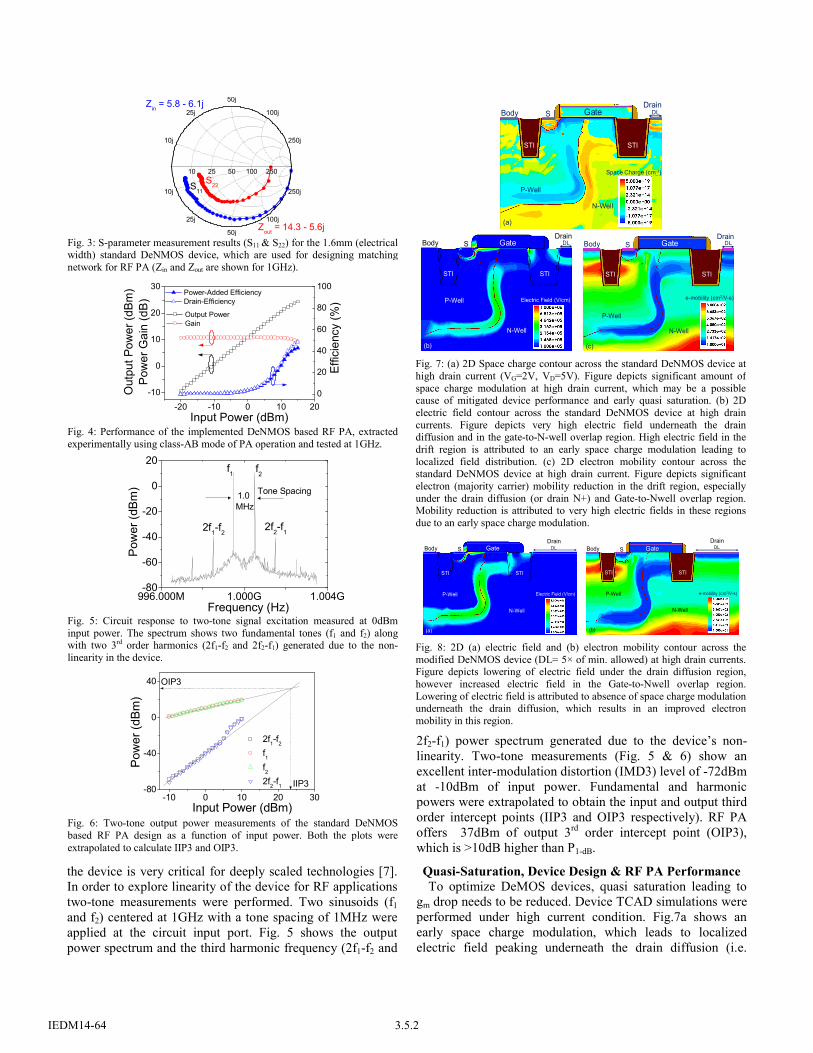
the device is very critical for deeply scaled technologies [7]. In order to explore linearity of the device for RF applications two-tone measurements were performed. Two sinusoids (f1 and f2) centered at 1GHz with a tone spacing of 1MHz were applied at the circuit input port. Fig. 5 shows the output power spectrum and the third harmonic frequency (2f1-f2 and
2f2-f1) power spectrum generated due to the device’s non-linearity. Two-tone measurements (Fig. 5 & 6) show an excellent inter-modulation distortion (IMD3) level of -72dBm at -10dBm of input power. Fundamental and harmonic powers were extrapolated to obtain the input and output third order intercept points (IIP3 and OIP3 respectively). RF PA offers 37dBm of output 3rd order intercept point (OIP3), which is >10dB higher than P1-dB.
Quasi-Saturation, Device Design & RF PA Performance To optimize DeMOS devices, quasi saturation leading to
gm drop needs to be reduced. Device TCAD simulations were performed under high current condition. Fig.7a shows an early space charge modulation, which leads to localized electric field peaking underneath the drain diffusion (i.e.
Fig. 3: S-parameter measurement results (S11 & S22) for the 1.6mm (electricalwidth) standard DeNMOS device, which are used for designing matchingnetwork for RF PA (Zin and Zout are shown for 1GHz).
-20 -10 0 10 20
-10
0
10
20
30
Out
put P
ower
(dB
m)
Pow
er G
ain
(dB
)
Input Power (dBm)
Output Power Gain
0
20
40
60
80
100 Power-Added Efficiency Drain-Efficiency
Effi
cien
cy (%
)
Fig. 4: Performance of the implemented DeNMOS based RF PA, extractedexperimentally using class-AB mode of PA operation and tested at 1GHz.
996.000M 1.000G 1.004G-80
-60
-40
-20
0
20
1.0 MHz
2f2-f12f1-f2
f1
Pow
er (d
Bm
)
Frequency (Hz)
f2
Tone Spacing
Fig. 5: Circuit response to two-tone signal excitation measured at 0dBm input power. The spectrum shows two fundamental tones (f1 and f2) along with two 3rd order harmonics (2f1-f2 and 2f2-f1) generated due to the non-linearity in the device.
-10 0 10 20 30-80
-40
0
40
Pow
er (d
Bm
)
Input Power (dBm)
2f1-f2
f1 f2 2f2-f1 IIP3
OIP3
Fig. 6: Two-tone output power measurements of the standard DeNMOSbased RF PA design as a function of input power. Both the plots wereextrapolated to calculate IIP3 and OIP3.
10 25 50 100 250
10j
10j
25j
25j
50j
50j
100j
100j
250j
250j
Zout = 14.3 - 5.6j
S22S11
Zin = 5.8 - 6.1j
(a)
Fig. 7: (a) 2D Space charge contour across the standard DeNMOS device athigh drain current (VG=2V, VD=5V). Figure depicts significant amount ofspace charge modulation at high drain current, which may be a possiblecause of mitigated device performance and early quasi saturation. (b) 2Delectric field contour across the standard DeNMOS device at high draincurrents. Figure depicts very high electric field underneath the draindiffusion and in the gate-to-N-well overlap region. High electric field in thedrift region is attributed to an early space charge modulation leading tolocalized field distribution. (c) 2D electron mobility contour across thestandard DeNMOS device at high drain current. Figure depicts significantelectron (majority carrier) mobility reduction in the drift region, especiallyunder the drain diffusion (or drain N+) and Gate-to-Nwell overlap region.Mobility reduction is attributed to very high electric fields in these regionsdue to an early space charge modulation.
Fig. 8: 2D (a) electric field and (b) electron mobility contour across themodified DeNMOS device (DL= 5× of min. allowed) at high drain currents.Figure depicts lowering of electric field under the drain diffusion region,however increased electric field in the Gate-to-Nwell overlap region.Lowering of electric field is attributed to absence of space charge modulationunderneath the drain diffusion, which results in an improved electronmobility in this region.
Space Charge (cm-3)
DrainGateSBody
STI STI
DL
P-Well
N-Well
(a)
Electric Field (V/cm)
DrainGateSBody
STI STI
DL
P-Well
N-Well
(b)
e-mobility (cm2/V-s)
DrainGateSBody
STI STI
DL
P-Well
N-Well
(c)
Electric Field (V/cm)
DrainGateSBody
STI STI
P-Well
N-Well
(a)
DL
e-mobility (cm2/V-s)
DrainGateSBody
STI STI
P-Well
N-Well
(b)
DL
3.5.2IEDM14-64
drain N+) and within the gate-to-Nwell overlap region (Fig.7b). Increased electric field results in significant mobility reduction across these regions (Fig.7c). As the charge modulation takes place when mobile carriers exceed the background doping, reducing the current density in critical regions should mitigate space charge modulation. Increasing the drain N+, drain diffusion length (DL) successfully reduces current density and mitigates electric field peaking and electron mobility reduction (Fig. 8). This has resulted in an improved device with increased ON-current, lower on-resistance, increased trans-conductance and load line swing when compared to the standard device. The RF PA performance (Fig. 9-11), shows 45% improvement in RF gain and 25% improvement in PAE. Fig. 10b shows 40% reduction in the on-resistance of the DeNMOS device by drain engineering.
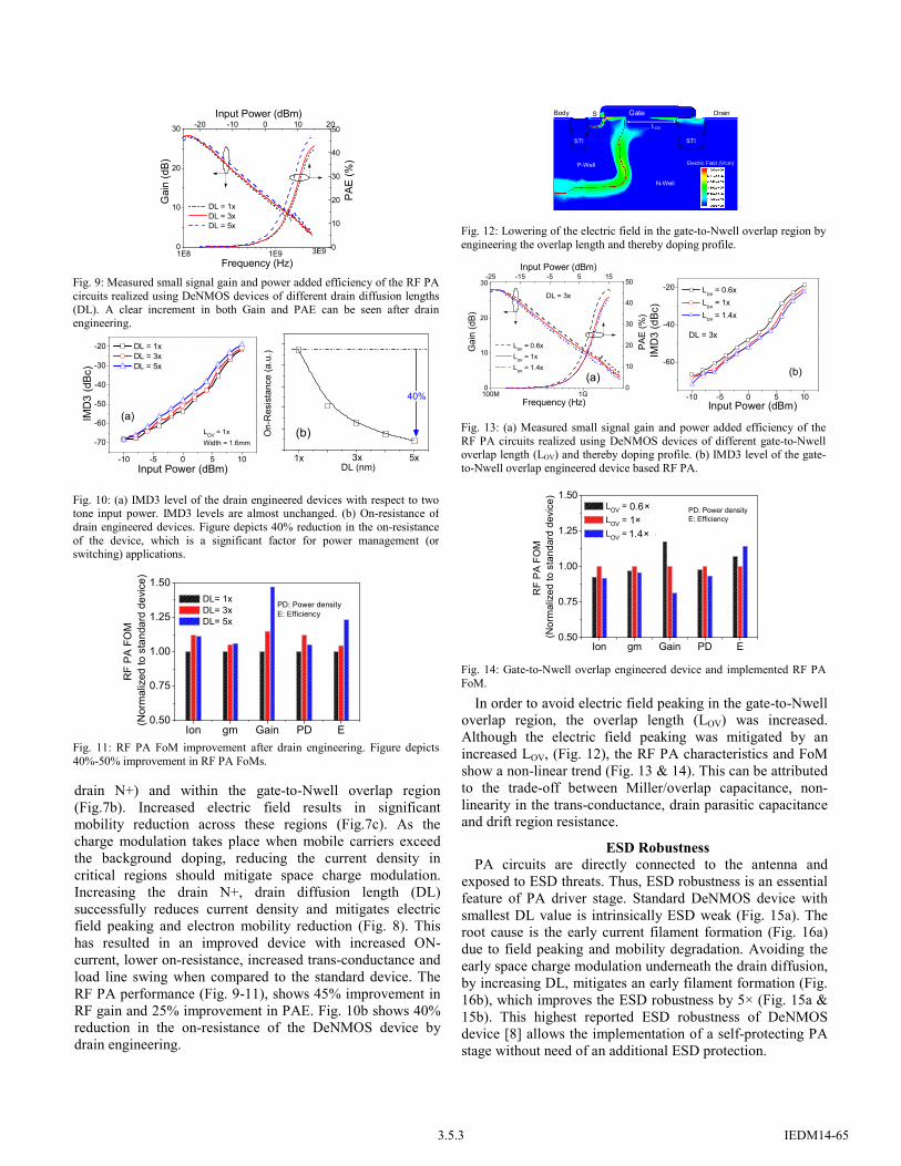
In order to avoid electric field peaking in the gate-to-Nwell overlap region, the overlap length (LOV) was increased. Although the electric field peaking was mitigated by an increased LOV, (Fig. 12), the RF PA characteristics and FoM show a non-linear trend (Fig. 13 & 14). This can be attributed to the trade-off between Miller/overlap capacitance, non-linearity in the trans-conductance, drain parasitic capacitance and drift region resistance.
ESD Robustness PA circuits are directly connected to the antenna and
exposed to ESD threats. Thus, ESD robustness is an essential feature of PA driver stage. Standard DeNMOS device with smallest DL value is intrinsically ESD weak (Fig. 15a). The root cause is the early current filament formation (Fig. 16a) due to field peaking and mobility degradation. Avoiding the early space charge modulation underneath the drain diffusion, by increasing DL, mitigates an early filament formation (Fig. 16b), which improves the ESD robustness by 5× (Fig. 15a & 15b). This highest reported ESD robustness of DeNMOS device [8] allows the implementation of a self-protecting PA stage without need of an additional ESD protection.
1E8 1E90
10
20
30
Gai
n (d
B)
Frequency (Hz)
DL = 1x DL = 3x DL = 5x
3E9
-20 -10 0 10 20
0
10
20
30
40
50
PA
E (%
)
Input Power (dBm)
Fig. 9: Measured small signal gain and power added efficiency of the RF PAcircuits realized using DeNMOS devices of different drain diffusion lengths(DL). A clear increment in both Gain and PAE can be seen after drainengineering.
-10 -5 0 5 10
-70
-60
-50
-40
-30
-20
IMD
3 (d
Bc)
Input Power (dBm)
DL = 1x DL = 3x DL = 5x
LOV = 1xWidth = 1.6mm
(a)
50 100 150 200 250
On-
Res
ista
nce
(a.u
.)
DL (nm)
40%
1x 3x 5x
(b)
Fig. 10: (a) IMD3 level of the drain engineered devices with respect to two tone input power. IMD3 levels are almost unchanged. (b) On-resistance of drain engineered devices. Figure depicts 40% reduction in the on-resistance of the device, which is a significant factor for power management (orswitching) applications.
Ion gm Gain PD E0.50
0.75
1.00
1.25
1.50
RF
PA F
OM
(N
orm
aliz
ed to
sta
ndar
d de
vice
)
DL= 1x DL= 3x DL= 5x
PD: Power densityE: Efficiency
Fig. 11: RF PA FoM improvement after drain engineering. Figure depicts40%-50% improvement in RF PA FoMs.
Fig. 12: Lowering of the electric field in the gate-to-Nwell overlap region byengineering the overlap length and thereby doping profile.
100M 1G0
10
20
30
Gai
n (d
B)
Frequency (Hz)
Lov = 0.6x Lov = 1x Lov = 1.4x
DL = 3x
-25 -15 -5 5 15
0
10
20
30
40
50
Input Power (dBm)
PA
E (%
)
(a)-10 -5 0 5 10
-60
-40
-20
IMD
3 (d
Bc)
Input Power (dBm)
Lov = 0.6x Lov = 1x Lov = 1.4x
DL = 3x
(b)
Fig. 13: (a) Measured small signal gain and power added efficiency of theRF PA circuits realized using DeNMOS devices of different gate-to-Nwelloverlap length (LOV) and thereby doping profile. (b) IMD3 level of the gate-to-Nwell overlap engineered device based RF PA.
Fig. 14: Gate-to-Nwell overlap engineered device and implemented RF PAFoM.
Electric Field (V/cm)
DrainGateSBody
STI STI
P-Well
N-Well
LOV
Ion gm Gain PD E0.50
0.75
1.00
1.25
1.50
RF
PA
FO
M
(Nor
mal
ized
to s
tand
ard
devi
ce)
LOV = 170nm LOV = 280nm LOV = 400nm
PD: Power densityE: Efficiency
0.6×1×1.4×
3.5.3 IEDM14-65
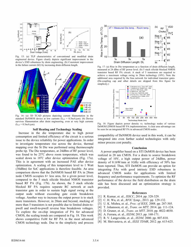
Self Heating and Technology Increase in the die temperature due
consumption and limited efficiency of the cissue to the device reliability for power applto investigate temperature rise across the mapping over the Si Die was performed usiprobe tip. The Die temperature, at 24dBm ofwas found to be 25oC above room temperascaled down to 18oC after device optimizThis is in agreement with an increased Poptimization. A scaling of this temperature(30dBm) for SoC applications is therefore comparison shows that the DeNMOS basednode CMOS occupies 6× less area, for a gicompared to the 5 stack silicide blocked Nbased RF PA (Fig. 17b). As shown, the blocked RF PA requires separate RC ntransistor gate in order to sustain high sigoutput node without exceeding gate ovoltage. Another way to increase the output more transistors. However, in 28nm and beymore than 5 transistors is not possible due topwell and nwell-to-pwell reverse bias breaTo explore the on-chip integration of PCMOS, the scaling trends are compared in Fshows competitive FoM for RF PA in theCMOS technology node. Due to the simpli
0 2000
1
2
3
4
It2 (m
A/μ
m)
4x
(b)
Fig. 15: (a) TLP characteristics of conventional engineered device. Figure clearly depicts significant device’s ESD robustness by drain engineering. (b) Conin the failure current (It2) by increasing drain diffusion l
Fig. 16: (a) 3D TCAD pictures depicting current standard DeNMOS device at low currents (ITLP = 0.5survives filamentation after drain engineering, even a(ITLP = 0.5mA/µm).
0 2 4 6 8 10 12 14 160.0
0.5
1.0
1.5
2.0
2.5
3.0
3.5
I TLP
(mA
/μm
)
Drain Voltage (Volts)
STIN+
P-Body
Gate Drain
1x
N-Well
STI N+
P-Body
Gate Drain
10x
N-Well
Current Density
N-Well
(a)
Z X
Y
(b)
Z
X
Y
Scaling to high power
ircuit is a serious lications. In order device, thermal ing thermocouple f RF power level, ature, which was
zation (Fig. 17a). PAE after device e level to 1 Watt feasible. An area
d RF PA in 28nm iven power level, NMOS transistor
5 stack silicide network at each gnal swing at the xide breakdown power is to stack yond, stacking of
o limited drain-to-akdown voltages.
PA for advanced Fig. 18. This work e most advanced icity and process
compatibility of DeNMOS device uintegrated into even further scaledminor process cost penalty.
ConclusiA power amplifier based on a STI
realized in 28 nm CMOS. For a drvoltage of 10V, a high output pdensity of 0.16W/mm at 1GHz witbeen reported. Thus, STI DeMOS cintegrating PAs with good intrinadvanced CMOS nodes for apfrequency and performance requiremperformance of the device the fieldside has been discussed and an provided.
Referenc[1] R. Kumar, et. al., ISSCC, 2014. [2] C. H. Wu, et. al., RFIC Symp., 2[3] U. K. Mishra, et. al., Proc. of IE[4] T. Johansson, et. al., Trans. on M[5] D. Gruner, et. al., Trans. on MT[6] A. Ferrara, et. al., IEDM, 2013. [7] R. V. Langevelde, et. al., IEDM[8] M. Shrivastava, et. al., IEEE TD
0 400 600 800 1000
Width = 9μm Width = 450μm Width = 1.6mm Fitting
DL (a.u.)x 8x 12x 16x 20x
and modified drainimprovement in the
nsistent improvementlength.
filamentation in the5mA/µm). (b) Device at very high currents
Current Density
0 1 2 3 4 515
20
25
30
x
dT = Measured Die temp. - Room
Ris
e in
Die
Tem
p.: d
T (o C
)
Drain Diffusion Length: DLx
(a)
Fig. 17: (a) Rise in Die temperature as a funmeasured at 24 dBm of RF power level. (b) transistor based RF PA circuit. A stack oachieve a maximum voltage swing in 28nmadditional area required by the bias network(De-coupling cap and other details are simplicity.)
0 50 100 150 200 2500.0
0.5
1.0
1.5
O. Bengtsson et al., Tra L. Vestling et al., EUMW J. Ko et al., RFIC Symp D. Muller et al., TED, 2 E. Chen et al., RAWCO H. M. Hsu et al., Trans T. Johansson et al., Eu This work (2014)
Pow
er D
ensi
ty (W
/mm
) x F
requ
ency
(GH
z)
Technology Node
28nm CMOS (This work)
Fig. 18: Figure depicts power density vs.DeMOS/LDMOS based RF PA implementatibe seen for an integrated RF PA in advanced
used in this work, it can be d technologies with only
ion I DeMOS device has been rain to source breakdown
power of 24dBm, power th efficiency of 50% has can provide an option for nsic ESD robustness in pplications with limited ments. To optimize the RF d distribution on the drain
optimization strategy is
ces pp. 328-329.
2013. pp. 129-132. EEE, 2008. pp. 287-305. MTT, 2014. pp. 111-124.
TT, 2010. pp. 4022-4030. pp. 168-171.
M, 2000. pp. 807-810. DMR, 2012. pp. 615-625.
5 6x
temp.
L
)
nction of drain diffusion length, 5 stack silicide blocked NMOS f 5 transistors are required to m technology (10V). Note the
k for individual transistor gates. skipped from this figure for
0 300 350 400
ans. MTT, 2003W Conf., 1999p., 2005007
ON, 2000. MTT, 2002
uMIC, 2013
(nm) technology nodes of various ions. A clear area advantage can CMOS nodes.
3.5.4IEDM14-66