Embed Size (px)
Citation preview

Basic Electrical Properties of MOS, BiCMOS Devices
CHAPTER OBJECTIVES
In this chapter, you will be introduced to
Operation and characteristics of MOSFET• • Threshold voltage of MOSFET
Leakage currents in MOSFET• • Transconductance, output conductance and figure of merit of MOSFET• Pass transistor logic
nMOS inverter and its characteristics• CMOS • inverter and its characteristicsBiCMOS inverters•
• Latch up in CMOS devices
2.1 INTRODUCTION OF MOSFET
The rapid strides of the semiconductor industry in recent years are due to its ability to incorpo-rate more and more devices operating at higher and higher speeds in an IC. Metal Oxide Field Effect Transistor (MOSFET) circuits occupy less silicon area and consume less power than their bipolar counterparts (BJT) making them ideal choice for VLSI circuits. The MOSFET was the subject of a patent in 1933, but did not reach commercial maturity until about thirty years later. The delay was principally due to a lack of understanding of the importance of the oxide/semiconductor interface, and to the time taken to develop suitable fabrication procedures, notably for the growth of the thin gate oxide.
22CHAPTER

Basic Electrical Properties of MOS, BiCMOS Devices 47
Referring to Fig. 2.2,
MOSFET’s are made from crystalline semiconductor that forms the host structure called • the substrate or bulk of the device. Substrate for nMOS is p-type silicon whereas for the pMOS devices it is n-type silicon. The thin oxide of the transistor electrically isolates the gate from the semiconductor • underneath. The gate oxide is made of oxidized silicon forming non-crystalline, amor-phous SiO2. The gate oxide thickness is typically from near 15 Å to 100 Å. Drain and source regions are made from crystalline silicon by implanting a dopant with • opposite polarity to that of the substrate. In pMOS, boran impurities are doped and in nMOS phosphorous impurities are doped. The gate is fabricated using polysilicon or metal. Since drain and drain dopants are made of opposite polarity to the substrate (bulk) they form pn junction diodes that are reverse biased in normal operation of the device. This is shown in the Fig. 2.3.The gate is the control terminal and the source provides the electrons (nMOS) or holes • (pMOS) that are collected by the drain.The distance from drain to source is a geometrical parameter called channel length • (L) where the conduction takes place. Another geometrical parameter of the device is transistor channel width (W ). These two parameters are set by the circuit engineer. Other parameters such as oxide thickness, threshold voltage and doping levels depend • on the fabrication process and cannot be changed by the design. They are technology parameters.Complementary Metal Oxide Semiconductor (CMOS) logic circuits have both nMOS and • pMOS devices which will be discussed later in this chapter.
Fig. 2.3 Cross-sectional view of nMOSFET and pMOSFET.
2.1.2 Understanding Enhancement Mode MOSFET Operation: A Descriptive Approach
Transistor terminals must have proper voltage polarity to operate correctly. In MOSFETs, the terminal voltages are usually referred with respect to the source. The same convention will be followed in this chapter, i.e., the model equations will be developed with respect to VGS, VDS, and VSB. The positive convention current in nMOS (pMOS) device is from drain (source) to the source (drain) and is referred as IDS or ID. When a positive (negative) voltage is applied to the drain terminal; the drain current depends on the voltage applied to the gate control terminal.

Basic Electrical Properties of MOS, BiCMOS Devices 49
2.1.2.3 Threshold Voltage
Since the drain and source are at the same voltage the channel carrier distribution is • uniform along the device. The voltage at which the surface of the semiconductor gets inverted to the opposite polarity is known as Threshold voltage. In nMOS transistor, the surface will be inverted to n-type (remember in nMOS bulk is p-type silicon) and for pMOS transistor the surface will be inverted to p-type (remember in pMOS bulk is n-type silicon). At the threshold voltage condition, the concentration of electrons (holes) accumulated near the surface in a nMOS (pMOS) is equal to the doping concentration of the bulk doping concentration. Threshold voltage for nMOS is always positive and threshold voltage for pMOS is always negative. An nMOS (pMOS) transistor has a conducting channel when the gate-source voltage is • greater than (less than) threshold voltage, i.e., VGS > Vtn (VGS < Vtp).
Let us discuss in detail about the threshold voltage of an nMOSFET.In a MOSFET since all terminal voltages are applied with respect to the source the thresh-
old voltage is also measured with respect to source.
The threshold voltage of a MOSFET is defined as the value of gate to source voltage which is sufficient to produce a surface inversion layer when VDS = 0 V.
orThe voltage at which the surface of the semiconductor gets inverted to the opposite polar-
ity is known as threshold voltage.
VSB is applied to the MOSFET and is always positive or greater than zero. VSB is applied to keep the pn junctions in the MOSFET reverse biased so that no substrate current flows in the device into the bulk/substrate. For a MOSFET the surface is inverted (channel is formed) when the surface potential is Ψs = 2φB + VSB. The formula for threshold voltage is given by
V VqN
Cth FB BA si B SB
ox= + 2
2 2φ
φ+
∈ +( V ) (2.1)
VFB = flat band voltage equal to φmsφms = work function difference between gate and substrateNA = substrate doping concentrationφB = energy difference between the Fermi level and intrinsic Fermi level in the semicon-
ductor (silicon here) or Fermi voltageCox = oxide capacitance per unit area given by ∈ox /tox where tox is the thickness of the
oxide.
The surface gets inverted when the surface potential Ψs = 2φB + VSB in case of a MOSFETVth is a function of several components, most of which are material constants such as the differ-
ence in work function between gate and substrate material, the oxide thickness, the Fermi voltage. Apart from them the parameters shown below will also show their effect on the threshold voltage.
50 VLSI Design
If in the fabrication process some charges (sodium ions through human sweat, etc.) are • trapped in the gate oxide, threshold voltage is altered as they show their reaction to the volt-age applied to the gate. For example, if some positive ions are fixed in the oxide, the amount of positive charge required near the gate terminal to invert the surface decreases, hence threshold voltage decreases.
If Qf is the charge in the oxide, the amount of extra voltage to be applied to the gate to neutralize these charges is given by – (Qf /Cox).Once the MOSFET is fabricated and if the threshold voltage has to be adjusted (increase • or decrease) the only solution is to implant the dopants near the surface. This is known as threshold voltage adjustment implant and is given by VII = qDI/Cox. qDI is the charge implanted in the channel per unit area.The final expression with the above two effects included is given by•
V VqN V
CQC
qDCth FB B
A si SB
ox
f
ox
I
ox= + +
∈ +− +2
2 2φ
φ( )B (2.2)
Body effect parameter (γ)
Equation (2.2) shows that when VSB = 0 the threshold voltage reduces for the MOSFET reduces to that for the corresponding MOS capacitor. The effect of VSB on the threshold voltage can be expressed through the relation
∆V V V Vth th tho B SB B= − = ( )γ φ + − φ2 2 (2.3)
ΔVth = change in threshold voltage due to the application of substrate bias. γ is called the body effect parameter given by
γ =2qN
CA si
ox
∈ (2.4)
From the above equation, we see that the body effect which is change in Vth due to sub-strate bias is more pronounced in MOSFETs with higher NA and tox.
For a typical long channel nMOSFET when the channel forms in the nMOS (pMOS) tran-sistor, a positive (negative) drain voltage with respect to the source creates a horizontal elec-tric field, moving the electrons from source towards the drain forming a positive (negative) drain current. If the horizontal electric field is of same order or smaller than the vertical one, the inversion channel remains almost uniform along the device length. This happens when
VDS < (VGS – Vtn) for nMOS transistor VDS > (VGS – Vtp) for pMOS transistor (2.5)
The above threshold current in MOSFETs is primarily drift current. The inversion layer behaves as a resistance and as VDS is increased initially from 0 V, the drain current IDS increases linearly.
Note: Threshold voltage is generally denoted by Vt. If it is for nMOSFET we denote as Vtn and if it is for pMOSFET, we denote by Vtp.

Basic Electrical Properties of MOS, BiCMOS Devices 51
In this condition, the vertical electric field dominates the horizontal one. The transistor is in its linear region and is known as ohmic or non-saturated region. This is shown in Fig. 2.5(a).
2.1.2.4 Saturation RegionUltimately when VDS = VDsat, the voltage across the oxide near the drain end is no longer suf-ficient to support the channel (inversion layer), i.e., the horizontal electric field becomes stron-ger than the vertical electric field at the drain end. The conducting channel retracts from the drain and no longer “touches” this terminal. When this happens the inversion channel is said to be “pinched off ” and the device is in the saturation region. This is shown in Fig. 2.5(b).In this region the pinch off point moves towards the source as VDS increases. The voltage at the pinch off point remains VDsat. The extra voltage VDS – VDsat is now dropped in the deple-tion region. The electrons which reach the pinch off point are swept across to the drain by the electric field in the depletion region. The current in the saturation region remains almost fixed as the voltage across the inversion layer is fixed at VDsat. A small increase in the current is observed due to the shift of pinch off point towards the source end, which effectively reduces the channel length of the MOSFET from L to L′ as shown in Fig. 2.5(c).
The conditions for pinch off is
VDS ≥ (VGS – Vtn) for nMOS transistor
VDS ≤ (VGS – Vtp) for pMOS transistor. (2.6)
Fig. 2.5 Various regions of operation of MOSFET (a) ohmic region (b) onset of saturation region (c) saturation region.
52 VLSI Design
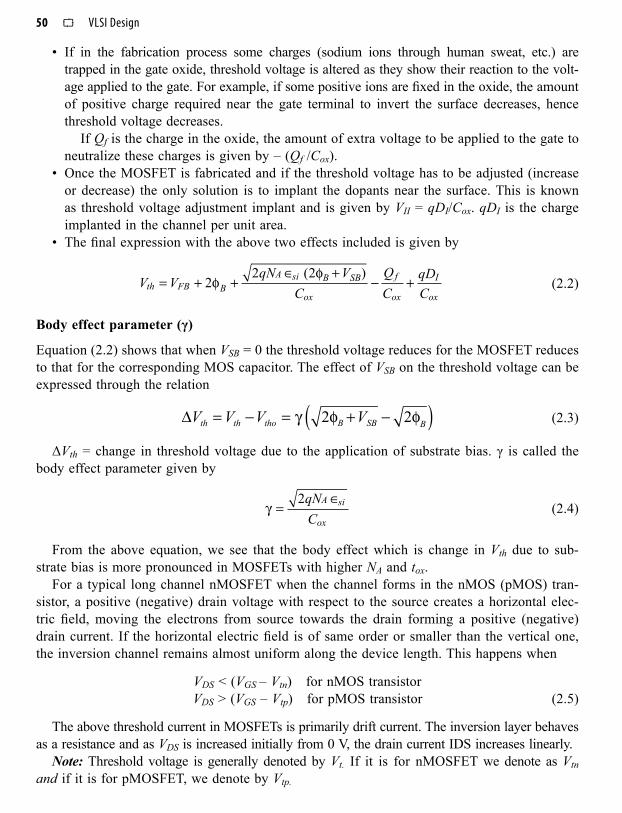
The behaviour of MOS transistor in different operation regions is best understood by analy-sis of its current voltage characteristics. The following chart in Fig. 2.6 shows the behaviour of an nMOSFET whose channel length L is 10 µm.
Fig. 2.6 I-V characteristics of long channel nMOSFET for various VGS values.
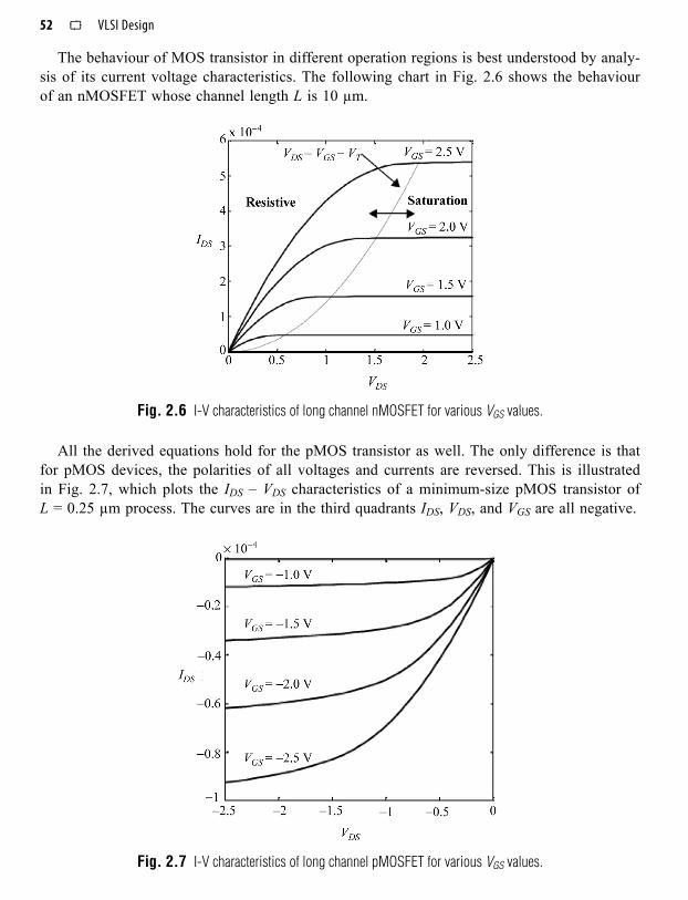
All the derived equations hold for the pMOS transistor as well. The only difference is that for pMOS devices, the polarities of all voltages and currents are reversed. This is illustrated in Fig. 2.7, which plots the IDS – VDS characteristics of a minimum-size pMOS transistor of L = 0.25 µm process. The curves are in the third quadrants IDS, VDS, and VGS are all negative.
Fig. 2.7 I-V characteristics of long channel pMOSFET for various VGS values.

Basic Electrical Properties of MOS, BiCMOS Devices 53
The mobility of holes in silicon is typically lower than that of the electrons. This means that pMOS transistors provide less current than nMOS transistors of comparable size and hence are slower.
2.1.2.5 Current Equations of MOSFET in Various Regions of OperationLet us discuss a first order (ideal Shockley) model relating the current and voltage for an nMOSFET in ohmic or nonsaturated regions.
In a• cut-off region (VGS < Vtn) there is no channel and almost zero current flows from drain to source. In other regions, the gate attracts carriers (electrons) to form the channel. The electrons drift • (drift current means current under the influence of the electric field) from source to drain at a rate proportional to the electric field between these regions. Thus, we can compute the currents if we know the amount of charge in the channel and the rate at which it flows.
We know that the charge on capacitor’s plate is Q = CV. Thus, the charge in the channel Qchannel is
Qchannel = Cg (VGC – Vtn) (2.7)
Cg is capacitance of gate to the channel; VGC – Vtn is the amount of voltage attracting charge to the channel beyond threshold voltage.
If the source is at VS and drain is at VD, the average is
V V VC
S= + D
2 (2.8)
Let us do a small calculation, i.e., adding and subtracting VS
V V V V V V VC
S S S DS
DS= + − + = +2 2
(2.9)
Therefore, the mean difference between gate and channel potentials is VGC = (VGS + VGD)/2
V V V V V V
V V V
V V
GC G C G SDS
G SDS
GSDS
= − = − +
= − −
= −
22 9
2
2
from ( . )
(2.10)
We can model the gate as a parallel plate capacitor with capacitance proportional to area over thickness. If the gate has length L and width W and oxide thickness is tox , the capacitance is given by
C WLtg oxox
= ε (2.11)
where εox = 3.9 εo for silicon dioxide and εo is the permittivity of free space which is 8.85 × 10⁻⁴ F/cm.

54 VLSI Design
Consider the Fig. 2.8 given below.
Each carrier in the channel (here electrons) is accelerated to an average velocity propor-tional to the lateral electric field, i.e., lateral electric field between the source and the drain. The constant of proportionality µ is known as mobility of the carriers. As electrons are carriers here, we write µ as µn
v = µnE (2.12)
The electric field E is the voltage difference between drain and source VDS divided by the channel length.
E VLDS= (2.13)
The time required for the carriers (electrons) to cross the channel is the channel length divided by the carrier velocity.
t = L / v (2.14)
Therefore, the current between drain and source VDS is the total amount of charge in the channel divided by the time required to cross the channel
I QtDS = channel (2.15)
I QL vDS = channel
/ (2.16)
We know Qchannel = Cg (VGC – Vtn) and substituting the value of VGC in the equation, and substituting the values of we obtain L and v from equations 2.11 and 2.13 we obtain the below expression for IDS
I C WL
V V V VDS n ox GS tn DS DS= − −( )µ 2 (2.17a)
Fig. 2.8 MOSFET.

Basic Electrical Properties of MOS, BiCMOS Devices 55
The equation can be rewritten as
I V V V V C WLDS GS tn DS DS n ox= − −( )β β µ2 where = (2.17b)
Equation 2.17(a) describes the linear region of operation for VGS > Vtn but VDS is very small. IDS increases almost linearly with VDS just like an ideal resistor. The geometry and tech-nology parameters are sometimes merged into a single factor. This symbol is not the same as symbol used for ratio of collector to base current in a bipolar transistor.
When VDS is further increased, at the value of VDS = VGS – Vtn the drain current begins to become constant. This voltage is known as saturation voltage VDsat. At this point the IR drop in the device equals the effective gate to channel voltage at the drain. If VDS is further increased beyond VDsat, IDS becomes constant. The channel pinches off from drain towards source with the increase of VDS beyond VDsat. Substituting the value of VDsat = VGS – Vtn in equation 2.17(b).
I V V V V
V V
DS GS tn Dsat Dsat
GS tn
= − −( )= −( )
β
β2
22
(2.18)
It is sometimes convenient to define IDsat as the current of the transistor that is fully ON, i.e., VGS = VDS = VDD (supply voltage)
I V VDS DD tn= −( )β2
2 (2.19)
SUMMARY: Shockley 1st order transistor models
I
V VV V V V V V
V V
DS
GS t
GS tn DS DS DS Dsat
GS t
=
<− −( ) <
−
0
2
2
cutoff
β
β
linear
nn DS DsatV V( ) ≥
2 saturation
(2.20)
2.1.3 Understanding the Depletion Mode MOSFET Operation
Depletion mode MOSFET is normally continuous ON device. The depletion mode MOSFET has a narrow n-channel buried between the source and drain near the surface (in case of nMOSFET), i.e., n-types dopants are implanted near the surface. Free electrons are available in the channel area. With VDS = 0 a negative gate voltage attracts holes from the bulk into the channel near the surface. The recombination of induced holes with the existing electrons (from the buried channel) causes depletion of majority carriers. This action is responsible for its name as depletion mode MOSFET. If the gate voltage is made more negative majority carriers can be virtually depleted and channel is eliminated. The device is off in this condition. Under these circumstances drain
56 VLSI Design
current is zero. The least negative value of VGS for which channel is depleted is known as thresh-old voltage Vth of the MOSFET.
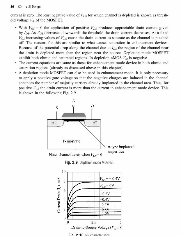
With • VGS = 0 the application of positive VDS produces appreciable drain current given by IDS. As VGS decreases downwards the threshold the drain current decreases. At a fixed VGS increasing values of VDS cause the drain current to saturate as the channel is pinched off. The reasons for this are similar to what causes saturation in enhancement devices. Because of the potential drop along the channel due to IDS the region of the channel near the drain is depleted more than the region near the source. Depletion mode MOSFET exhibit both ohmic and saturated regions. In depletion nMOS Vtn is negative.The current equations are same as those for enhancement mode device in both ohmic and • saturation regions (already as discussed above in this chapter).A depletion mode MOSFET can also be used in enhancement mode. It is only necessary • to apply a positive gate voltage so that the negative charges are induced in the channel enhances the number of majority carriers already implanted in the channel area. Thus, for positive VGS the drain current is more than the current in enhancement mode device. This is shown in the following Fig. 2.9.
Fig. 2.9 Depletion mode MOSFET.
Fig. 2.10 I-V characteristics.

Basic Electrical Properties of MOS, BiCMOS Devices 57
Help Desk
What is channel length modulation?When the drain voltage exceeds VDsat the pinch off point (also called as velocity
saturation point) moves from the drain towards the source and a depletion layer exists between this point and the drain. This movement is referred as channel length modula-tion. Considering channel length modulation, the drain current is given by the relation
I V V VD GS tn DS= −( ) +β λ2
12 ( ) (2.21)
where λ is channel length modulation parameter.
When the channel is pinched off near the drain end, there is no physical channel between the pinch off point and drain end. But the current remains constant. How does it happen?
Although there are no inversion charges at the drain end of the channel at the pinch off point, the drain region is electrically active. Carriers drift from the source and move under the effect of the horizontal electric field. Once they arrive at the pinch off point of the channel they travel from that point to the drain driven by the high electric field of the depletion region. This is drift current in the device which is almost constant.
Write down the importance of threshold voltage in a MOSFET and how is it dependent on oxide thickness, and doping concentration of the substrate.
The threshold voltage of a MOSFET is usually defined as the gate voltage where an inversion layer forms at the interface between the insulating layer (oxide) and the substrate (body) of the transistor. It is given by
V VqN
Cth FB BA si B
ox= + +
∈2
2 2φ
φ( + )VSB (2.22)
Threshold voltage depends on the choice of oxide and on oxide thickness. Using the formulas above, Vtn is directly proportional to γ, and tox, which is the parameter for oxide thickness. Thus, the thinner the oxide, the lower the threshold voltage.
The threshold voltage increases with the increase in the NA since the potential drop across oxide and surface both increase.
What is subthreshold leakage current?Subthreshold leakage or subthreshold conduction or subthreshold drain cur-
rent is the current that flows between the source and drain of a MOSFET when the transistor is in the subthreshold region, i.e., for gate-to-source voltages below the threshold voltage.
58 VLSI Design
2.1.4 Leakage Current Problem in the MOSFET
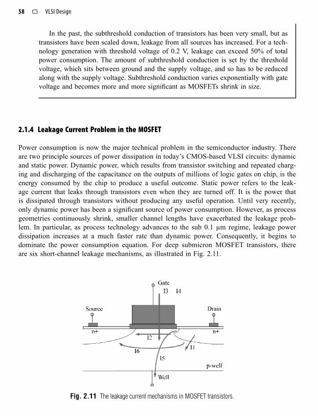
Power consumption is now the major technical problem in the semiconductor industry. There are two principle sources of power dissipation in today’s CMOS-based VLSI circuits: dynamic and static power. Dynamic power, which results from transistor switching and repeated charg-ing and discharging of the capacitance on the outputs of millions of logic gates on chip, is the energy consumed by the chip to produce a useful outcome. Static power refers to the leak-age current that leaks through transistors even when they are turned off. It is the power that is dissipated through transistors without producing any useful operation. Until very recently, only dynamic power has been a significant source of power consumption. However, as process geometries continuously shrink, smaller channel lengths have exacerbated the leakage prob-lem. In particular, as process technology advances to the sub 0.1 µm regime, leakage power dissipation increases at a much faster rate than dynamic power. Consequently, it begins to dominate the power consumption equation. For deep submicron MOSFET transistors, there are six short-channel leakage mechanisms, as illustrated in Fig. 2.11.
In the past, the subthreshold conduction of transistors has been very small, but as transistors have been scaled down, leakage from all sources has increased. For a tech-nology generation with threshold voltage of 0.2 V, leakage can exceed 50% of total power consumption. The amount of subthreshold conduction is set by the threshold voltage, which sits between ground and the supply voltage, and so has to be reduced along with the supply voltage. Subthreshold conduction varies exponentially with gate voltage and becomes more and more significant as MOSFETs shrink in size.
Fig. 2.11 The leakage current mechanisms in MOSFET transistors.

Basic Electrical Properties of MOS, BiCMOS Devices 59
I1 is the reverse-bias p–n junction leakage. • I2 is the subthreshold leakage or the weak inversion current across the device. • I3 is the gate leakage or the tunnelling current through the gate oxide insulation. • I4 is the gate current due to hot-carrier injection.• I5 is gate-induced drain leakage (GIDL). • I6 is the channel punch through current. •
Among these currents, I2, I5, and I6 are off state leakage mechanisms since they only exist when the transistor is in off state. I1, I3, and I4 can occur on both on and off states.
The leakage currents are influenced by threshold voltage, channel dimensions (physical), channel/surface doping profile, drain/source junction depth, gate oxide thickness, and VDD.Currently, the two principle components of static power consumption are the subthreshold leakage I2 and gate leakage I3.
Most of the operations of modern VLSI chips can be classified into two modes: active and standby. During the active mode of circuit operation, the total power dissipation includes both the dynamic and static portions. While in the standby mode, the power dissipation is due to only the standby leakage current. Dynamic power dissipation consists of two components. One is the switching power due to the charging and discharging of load capacitance. The other is short-circuiting power due to the non-zero rise and fall time of input waveforms. The static power of a CMOS circuit is only determined by the leakage current through each transistor. In other words, dynamic power is related to the circuit switching activity. In contrast, static power is proportional to the total number of transistors in the circuit regardless of their switch-ing activities. In general, dynamic power dissipation is expressed as Pdyn = αfCVDD
2, where α is the circuit switching activity, f is the operation frequency, C is the load capacitance, and VDD is the supply voltage. In the past several decades, as CMOS devices scaled down, supply voltage VDD also been trimmed down to keep the power consumption under control (since the power usage has quadratic dependence on VDD, according to the equation).
Accordingly, the transistor threshold voltage has to be commensurately scaled to maintain a high drive current and achieve performance improvement. However, this threshold voltage scaling also results in a substantial increase in subthreshold leakage current. Consequently, leakage power becomes a significant component of the total power consumption in both the active and standby modes of operation. To suppress the power consumption in deep-sub micrometre circuits, it is nec-essary to reduce the leakage power in both the active and standby modes of operation. The reduc-tion in leakage current can be achieved using both process-level and circuit-level techniques.
At the process level, leakage reduction can be achieved by controlling the dimensions (length, oxide thickness, and junction depth) and doping profile in transistors. At the circuit level, threshold voltage and the leakage current of transistors can be effectively controlled by controlling the voltages of different device terminals (drain, source, gate, and body or sub-strate). In practice, several circuit design techniques have been suggested for leakage reduction in digital circuits (logic and memory), such as transistor stacking, multiple Vth, dynamic Vth.
If care is not taken, leakage power can lead to dramatic effects that may cause a circuit to fail to function properly. Large leakage current can increase the standby power dissipation to an unacceptable level or it can lead to excessive heating, which consequently requires complicated

60 VLSI Design
and expensive cooling and packaging techniques. In the beginning, only leading edge micro-processors were affected by this leakage current problem, but now leakage current has become a critical design parameter for all the nanometre chips. In summary, for modern VLSI chip design, the issue of controlling leakage current has moved from backstage to centre stage.
2.1.5 A.C. Properties: Transconductance, Output Conductance and Figure of Merit of a MOSFET
DefinitionsThe incremental resistances, transconductance and capacitances govern the a.c. properties of the MOSFET.
The transconductance gm is defined by
g IVm
DS
GS= ∂
∂ at constant VDS (2.23)
The small signal conductance or output conductance gd is given by
g IVd
DS
DS= ∂
∂ at constant VGS (2.24)
Linear region parameters and their importance in circuit performanceWhen the MOSFET is biased in linear region where VDS is small the conductance gd is obtained by differentiating equation 2.24 with respect to VDS
We know that I C WL
V V V VDS n ox GS tn DS DS= − −( )µ 2 (2.25)
Therefore, g C WL
V V Vdn ox
GS tn DS= − −( )µ and in linear region VDS << (VGS – Vtn) the above
equation simplifies to
g C WL
V V Vdn ox
GS tn DS= − −( )µ (2.26)
Present day VLSI circuits are MOSFET based as already discussed. The performance of the circuit depends on switching speed which in turn depends upon the parameter known as ON resistance given by
R Rg
LC W V VON channel
d n ox GS tn= = =
−( )1
µ (2.27)
To decrease the RON the width of the transistor has to be increased but that increases the area of the chip in return.
The transconductance defined above in equation 2.23 is obtained by differentiating with respect to VGS.
g C WL
V Vmn
DS DS= =µ βox (2.28)
62 VLSI Design
preferred for this application since the larger electron mobility implies faster switching than pMOSFETs. The basic nMOSFET pass transistor circuit is shown in the Fig. 2.12. The switch is controlled by VGS. If VGS = 0 then the transistor is off and there is no connection between the input and output. Placing a high voltage VG = VDD drives the nMOSFET active and current flows. For a logic 1 transfer, we use an input voltage Vin = VDD.
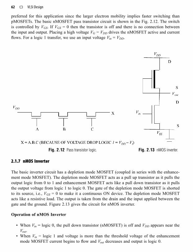
2.1.7 nMOS Inverter
The basic inverter circuit has a depletion mode MOSFET (coupled in series with the enhance-ment mode MOSFET). The depletion mode MOSFET acts as a pull up transistor as it pulls the output logic from 0 to 1 and enhancement MOSFET acts like a pull down transistor as it pulls the output voltage from logic 1 to logic 0. The gate of the depletion mode MOSFET is shorted to its source, i.e., VGS = 0 to make it a continuous ON device. The depletion mode MOSFET acts like a resistive load. The output is taken from the drain and the input applied between the gate and the ground. Figure 2.13 gives the circuit for nMOS inverter.
Operation of nMOS Inverter
When • Vin = logic 0, the pull down transistor (nMOSFET) is off and VDD appears near the Vout. When • Vin = logic 1 and voltage is more than the threshold voltage of the enhancement mode MOSFET current begins to flow and Vout decreases and output is logic 0.
Fig. 2.13 nMOS inverter.Fig. 2.12 Pass transistor logic.

Basic Electrical Properties of MOS, BiCMOS Devices 63
To obtain the transfer characteristics of the inverter, we superimpose the • VGS = 0 deple-tion mode characteristics curve on the family of curves for enhancement mode device. The points of intersection of the curves gives points on the transfer characteristics and is shown in the Fig. 2.14.The point at which • Vin = Vout is denoted by Vinv or switching threshold. The transfer characteristics (Fig. 2.15) and • Vinv can be shifted by changing the ratio of pull up to pull down impedances Zp.u / Zp.d. (impedance Z is denoted by ratio of length to width ratio of the transistor).Dissipation is high since rail to rail current flows when • Vin = Logical 1.Switching of output from 1 to 0 begins when • Vin exceeds Vtn of pull down device.When switching the output from 1 to 0, the pull up device is non-saturated initially and • pull down device moves to saturation.
Fig. 2.14 Derivation of nMOS inverter transfer characteristics.
Fig. 2.15 nMOS inverter transfer characteristics.

Basic Electrical Properties of MOS, BiCMOS Devices 65
We have
1 12 2
ZV
ZV V
p utd
p dinv tn
. .−( ) = −( ) (2.36)
V V VZ Z
inv tntd
p u p d= −
. ./ (2.37)
If we substitute the typical values in the above equation,
Vtn = 0.2VDD; Vtd = –0.6VDD; Vinv = 0.5VDD for equal marginsWe get,
Z Zp u p d. . // = 4 1 = 4/1
An inverter driven directly from the output of another should have • Z Zp u p d. . // = 4 1 ratio of ≥ 4/1.Similarly an inverter driven through one or more pass transistors as shown in the • Fig. 2.17 should have Z Zp u p d. . // = 4 1 ratio of ≥ 8/1 (Derivation is not given here)
Fig. 2.17 Pull up to pull down ratios for inverting logic by pass transistors.
2.1.8 CMOS Technology
Complementary metal oxide semiconductor (CMOS) is a major class of integrated circuits. CMOS technology is used in microprocessors, microcontrollers, static RAM, and other digital logic circuits. CMOS technology is also used for a wide variety of analog circuits such as image sensors, data converters, and highly integrated transceivers for many types of communications. In CMOS technology circuits, both n-type and p-type transistors are used to realize logic functions.
Two important characteristics of CMOS devices are high noise immunity and low static power consumption. Significant power is only drawn when the transistors in the CMOS device are switching between on and off states. Consequently, CMOS devices do not produce as much waste heat as other forms of logic, for example, transistor-transistor logic (TTL) or nMOS logic, which uses all n-channel devices without p-channel devices. These features allow inte-grating many more CMOS gates on an IC than in nMOS or Bipolar technology resulting in much better performance. The following Fig. 2.18 shows the CMOS logic circuit.

Basic Electrical Properties of MOS, BiCMOS Devices 67
Only transistor is ON connecting the output terminal Vout to one of the power rails, and there is no current in the circuit since the other transistor is off, thus eliminating a DC path between the rails. A capacitor load CL is shown in Fig. 2.19 and it is unavoidable in any cir-cuit. The capacitance is from transistor node and wiring capacitances.
Fig. 2.20 Transfer characteristics of CMOS inverter.
The nature and the form of the voltage-transfer characteristic (VTC) can be graphically deduced by superimposing the current characteristics of the nMOS and the pMOS devices.Such a graph is shown in the Fig. 2.20. Figure 2.21 shows current versus Vin in the CMOS inverter.
Fig. 2.21 CMOS inverter—current versus Vin.
Basic Electrical Properties of MOS, BiCMOS Devices 71
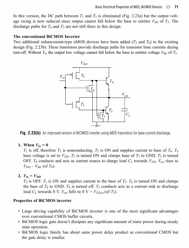
In this version, the DC path between T1 and T3 is eliminated (Fig. 2.23a) but the output volt-age swing is now reduced since output cannot fall below the base to emitter VBE of T3. The discharge paths for T4 and T3 are not still there in this design.
The conventional BiCMOS InverterTwo additional enhancement-type nMOS devices have been added (T5 and T6) to the existing design (Fig. 2.23b). These transistors provide discharge paths for transistor base currents during turn-off. Without T5, the output low voltage cannot fall below the base to emitter voltage VBE of T3.
Fig. 2.23(b) An improved version of BiCMOS inverter using MOS transistors for base current discharge.
1. When Vin = 0T1 is off, therefore T3 is nonconducting. T2 is ON and supplies current to base of T4. T4 base voltage is set to VDD. T5 is turned ON and clamps base of T3 to GND. T3 is turned OFF. T4 conducts and acts as current source to charge load CL towards VDD. Vout rises to VDD – VBE (of T4).
2. Vin = VDDT2 is OFF. T1 is ON and supplies current to the base of T3. T6 is turned ON and clamps the base of T4 to GND. T4 is turned off. T3 conducts acts as a current sink to discharge load CL towards 0 V. Vout falls to 0 V + VCEsat (of T3).
Properties of BiCMOS inverter
Large driving capability of BiCMOS inverter is one of the most significant advantages • over conventional CMOS buffer circuits.BiCMOS logic gate doesn’t dissipate any significant amount of static power during steady • state operation.BiCMOS logic family has about same power delay product as conventional CMOS but • the gate delay is smaller.
72 VLSI Design
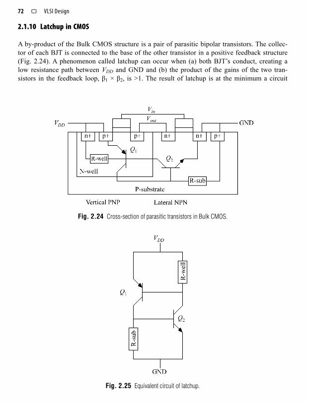
2.1.10 Latchup in CMOS
A by-product of the Bulk CMOS structure is a pair of parasitic bipolar transistors. The collec-tor of each BJT is connected to the base of the other transistor in a positive feedback structure (Fig. 2.24). A phenomenon called latchup can occur when (a) both BJT’s conduct, creating a low resistance path between VDD and GND and (b) the product of the gains of the two tran-sistors in the feedback loop, β1 × β2, is >1. The result of latchup is at the minimum a circuit
Fig. 2.24 Cross-section of parasitic transistors in Bulk CMOS.
Fig. 2.25 Equivalent circuit of latchup.

Basic Electrical Properties of MOS, BiCMOS Devices 73
malfunction, and in the worst case, the destruction of the device. The equivalent circuit is given in Fig. 2.25.
Latchup may begin when Vout drops below GND due to a noise spike or an improper circuit hookup (Vout is the base of the lateral NPN Q2). If sufficient current flows through R-sub to turn on Q2 (I R-sub > 0.7 V), this will draw current through R-well. If the voltage drop across R-well is high enough, Q1 will also turn on, and a self-sustaining low resistance path between the power rails is formed. If the gains are such that β1 × β2 > 1, latchup may occur. Once latchup has begun, the only way to stop it is to reduce the current below a critical level, usu-ally by removing power from the circuit.
Preventing latchup
1. Fab/Design Approaches
Reduce the gain product β1 × β2. Moving n-well and n+ source/drain farther apart increases width of the base of Q2 and
reduces gain β2 > also reduces circuit density. Buried n+ layer in well reduces gain of Q1.
2. Reduce the well and substrate resistances, producing lower voltage drops
Higher substrate doping level reduces R-sub. Reduce R-well by making low resistance contact to GND. Guard rings around p- and/or n-well, with frequent contacts to the rings, reduces the
parasitic resistances (Fig. 2.26).
Fig. 2.26 Guard rings for eliminating latchup.
Summary
1. Metal Oxide Field Effect Transistor (MOSFET) circuits occupy less silicon area and consume less power than their bipolar counterparts (BJT) making them ideal choice for VLSI circuits.

Basic Electrical Properties of MOS, BiCMOS Devices 77
We assumed that the transistor was in saturation, so we must check the result to see if that is true. For saturation,
VGS < VDS + Vtn
1.5 V < 1.355 V + 0.6 V
So the transistor is in saturation, and our assumption and answers are correct.
3. Repeat the above example, finding ID and VDS if VG = 1.8 V.Assume a transistor saturated state and
ID = (100 µA)(3)(1.8 – 0.6)2= 432 µA
VDS = 5 – (432 µA)(15 kΩ)= –1.48 V
This value for VDS is clearly not reasonable since there are no negative poten-tials in the circuit. Also, the bias check gives
VGS > VDS + Vtn
1.8V > –1.48 V + 0.6 V
The initial saturated state assumption was wrong, so we repeat the analysis using the ohmic state assumption:
ID = Kn (W/L) [2(VGS – Vth) VDS – VDS2]
= (100 µA) (3) [2(1.8 – 0.6) VDS – VDS2]
= 300 µA [2.4 VDS – VDS2]
This equation has two unknowns, so another equation must be found. We will use the KVL statement,
VDD = IDR + VDS
ID = (VDD – VDS)/R= (5 – VDS)/15 kΩ
The two equations can be equated to their ID solution, giving
(5 – VDS)/15 kΩ = 300 µA (2.4 VDS – VDS 2)
After some algebra, this reduces to
VDS2 – 2.622VDS + 1.11 = 0

78 VLSI Design
The two quadratic solutions are
VDS = 0.531 V, 2.09 V
The valid solution is VDS = 0.531 V, since this satisfies the nonsaturation condi-tion that was used in its solution:
VGS > VDS + Vtn
1.8 V > 0.531 V + 0.6 VID = (VDD – VDS)/15 kΩ
= (5 V – 0.531 V)/15 kΩ= 298 µA