Embed Size (px)
DESCRIPTION
Microcontoller ppt
Citation preview
N. Senthil Kumar,M. Saravanan & S. Jeevananthan
© Oxford University Press 2013
A Complete 8085 based system
© Oxford University Press 2013
• In the previous chapters-dealt -basic architecture, instruction set, programming -interfacing of peripherals.
• The individual peripherals-LEDs, seven segment displays, ADCs, DACs, Stepper motor, LCD displays and timers - interfacing with 8085
Introduction
© Oxford University Press 2013
• to build-complete system-memory and peripherals have to be interfaced with the processor-simultaneously.
• All these devices - work in synchronism with the processor without affecting each other. This chapter - the nuances of the interfacing all these devices to -complete system -execute the program in the desired manner.
Introduction contd..
© Oxford University Press 2013
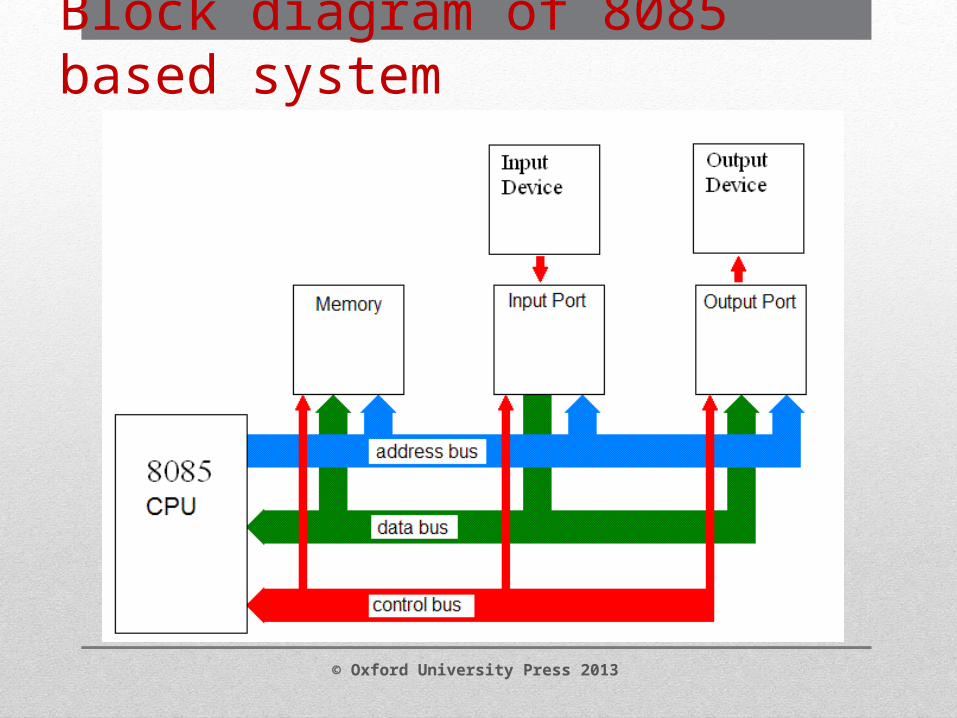
Block diagram of 8085 based system
© Oxford University Press 2013

• The system consists -8085 processor chip, memory chips, input device and an output device.
• The connecting wires between these parts are called as buses. • There are three different buses in the system - the address bus, the
data bus and control bus.
System Overview
© Oxford University Press 2013
• The address bus -transfer address from the processor to the memory and I/O ports.
• The CPU can select any one of the memory location or the I/O device by sending the corresponding address on these address lines.
• the 8085 processor - 16 address lines-can address 216 bytes or 64Kbytes of different addresses or memory locations
System Overview
© Oxford University Press 2013
• The 8085 processor used only 8 bit addresses for the I/O ports.• only 28 ports or 256 ports alone can be addressed. • The lower order address bus and the higher order bus contents -
same during the I/O port access in the 8085 address bus. • the CPU alone can send addresses to select the peripherals or
memory. So, the address bus is unidirectional -from CPU to the peripherals.
System Overview
© Oxford University Press 2013
• The data bus -transfer data between peripherals and the CPU. • The data bus is bidirectional as the data can flow in two directions. • All parts of -system transfer data through - data bus under -control
of the CPU. • The CPU -ensure that only one peripheral or memory chip transfers
data on the data bus. • The devices which are not using data bus must float its own data
bus.
System Overview
© Oxford University Press 2013
• This means that these devices must have their data bus in the high impedance state.
• In this state, the devices can neither source nor sink current. • So, the data bus will not be affected even though the device is
physically connected to it.
System Overview
© Oxford University Press 2013
• The control bus consists - various control signals from the processor to - peripherals and memory.
• These control signals - responsible for selecting the direction of data transfer.
• The memory and I/O selection -done by a proper control signal.• The peripherals - obey the control signals -by the processor.
System Overview
© Oxford University Press 2013
• Some -control signals are from - peripherals to the CPU. • An example -is the Ready signal. • This is -signal given out by a slow peripheral to the CPU.• If signal - low, then the processor will wait until the ready signal is
made high by the peripheral.
System Overview
© Oxford University Press 2013
• sequence of instructions or - is stored as binary numbers or codes in - successive memory locations.
• memory in a system must be at least of two types.• The ROM must be present -because the startup code, which is
executed when the power is on, must be resident in the memory permanently -so ROM is necessary.
System Overview
© Oxford University Press 2013
• Any system -has some programs stored permanently in ROMs -called Firmware.
• to store the temporary data during - program execution, Random Access memory or Read/ Write memory - RAM is necessary.
• So-system must have at least one ROM chip and a RAM chip. • The addressing of the memory locations -important and selection
of address for the ROM and RAM chips -important.
System Overview
© Oxford University Press 2013
• Memory in any microprocessor-based system is organized as a linear address space.
• In 8085, the memory is organized -starting address of 0000H to FFFFH.
• Program is organized as modules. Programmers write programs in different modules or different subroutines with specific functions.
• to organize the programs is -to write different subroutines or modules and then call them from the main program.
• So, any microprocessor based system - use the memory organization similar to that given in figure.
Address Map of a general 8085 system
© Oxford University Press 2013
Memory Organization in a microprocessor system
© Oxford University Press 2013
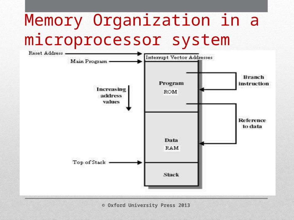
• the RESET -hardware signal applied to the microprocessor system for it to power on properly.
• Every system must be powered on with this signal.• Upon applying the Reset signal, the hardware resets itself and
makes the CPU execute the instructions present at predefined locations.
• The user must take control of the processor execution and so, must store the start-up program in the memory.
Memory Organization - Description
© Oxford University Press 2013
• This program must be stored in the ROM, so that it can be executed every time the processor is powered on.
• Therefore, at the reset address of the processor, an instruction to jump to the user start-up program is placed.
• The first few addresses are reserved for storing interrupt vector addresses.
• So all these locations contain jump instructions. • A ROM chip is used for storing the interrupt vector addresses and
the main program.
Memory Organization – Description contd..
© Oxford University Press 2013
• Some locations in the address map are reserved for the RAM chip. In addition to data, the RAM should be used for storing return addresses during interrupt and subroutine calls.
• Therefore, some amount of RAM should be allocated for the stack. • It can be seen that the system does not require all the possible 64
KB of memory. • The amount of memory is decided by the designers, depending
upon the application of the system
Memory Organization – Description contd..
© Oxford University Press 2013
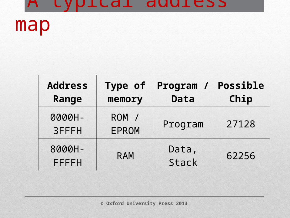
A typical address map
Address Range
Type of memory
Program / Data
Possible Chip
0000H- 3FFFH
ROM / EPROM
Program 27128
8000H-FFFFH
RAM Data, Stack 62256
© Oxford University Press 2013
A general 8085 based system
© Oxford University Press 2013
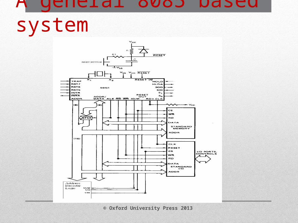
• The 8085 based system consists of standard memory and a standard I/O port interfaced to the 8085 processor.
• The 8085 processor operates - single power supply of +5V and Ground applied between Vcc and Vss.
• The 8085 processor has - internal clock generator. • It is enough to connect a crystal between the pins X1 and X2.
General microcomputer system using 8085
© Oxford University Press 2013
• The lower order address bus and data bus are multiplexed inside -processor.
• to access the address bus and data bus separately by the external devices, these buses –demultiplexed by connecting a latch to the multiplexed address and data bus.
• The Address Latch Enable (ALE) -signal given out by the processor to tell the latch that the address is sent out by the processor and is used to store the address in to the latch.
General microcomputer system using 8085
© Oxford University Press 2013
• RESET signal -be applied to the processor whenever the processor is switched on.
• So, a power on reset circuitry as shown -figure must be connected to the active low RESET input pin of the processor.
• The capacitor voltage at the power on -zero. So, an active low reset signal -to the processor.
• The reset signal should be applied - so that the reset action will be completed by the processor. The typical values of R and C are 75Kohms and 1micorfarads respectively.
General microcomputer system using 8085
© Oxford University Press 2013
• During normal operation, the capacitor -charged to the Vcc supply voltage and so the reset signal will not be applied to the processor.
• A bush button connected to the RC network is –reset signal manually.
• The R1 value is selected comparatively low when the reset push button is pressed, the capacitor will be discharged and an active low signal will be applied to RESET input.
General microcomputer system using 8085
© Oxford University Press 2013
• The control signals IO/M and RD and WR will be used for data transfer between peripherals and processor.
• The peripheral addressed by the processor is selected by -address decoder.
• The higher order address lines are used by - address decoder - select the desired chip of memory or I/O ports.
General microcomputer system using 8085
© Oxford University Press 2013
• The Address decoding is done –by higher order address lines A14 and A15 and control signal IO/M.
• The decoder IC 74139 can be used here. • 74139 - dual 2-4 decoder. The inputs -address lines A14 and A15.
The four outputs - active low outputs. • The enable input E -Gate input G1 and is an active low signal. So,
this chip -enabled when the IO/M signal is low for memory accesses.
General microcomputer system using 8085
© Oxford University Press 2013
• For the address map - the Y0 output -as the active low chip select for ROM.
• The outputs Y2 and Y3 must be combined using an AND gate to form the chip select for the RAM chip. The circuit diagram for this is given in figure 8.4
General microcomputer system using 8085
© Oxford University Press 2013
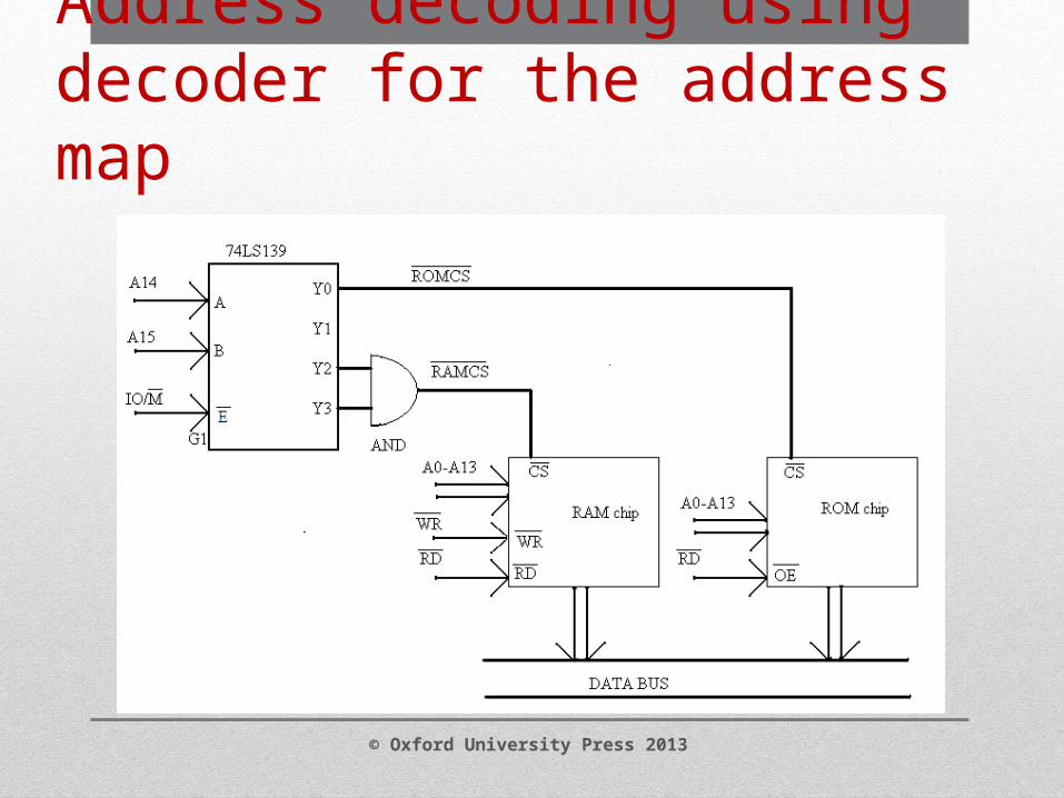
Address decoding using decoder for the address map
© Oxford University Press 2013
• A 8085 based system needs at least two I/O ports. One port -for an input device and another port for output device.
• The commonly used input device -keyboard matrix -the output device -multiplexed seven segment display.
• These two can be interfaced -processor using a single support chip -by Intel, the keyboard and display controller IC 8279. So, the system needs one 8279 chip.
General microcomputer system using 8085
© Oxford University Press 2013
• the system needs to interfacing of digital input and output ports. This is -supported by Intel’s programmable peripheral interface chip- IC8255.
• timing of events- -important issue in -microcomputer system -necessitates the use of a timer IC such as IC8253
• So, as an example three slave ICs 8279, 8255 and 8253 are considered for interfacing with 8085.
General microcomputer system using 8085
© Oxford University Press 2013
• To start -interfacing design, it is necessary to fix the address map for - devices to be interfaced.
• The address map assumed -three devices. Processor 8085 uses only 8 bits for I/O accesses.
• So, here 8-bit addresses -for the peripheral devices and The MSB 2 bits are selected to be different for the different chips.
• 8279 uses - two addresses whereas 8255 and 8253 - four addresses. The details of these interfacing -chapter 7.
General microcomputer system using 8085
© Oxford University Press 2013
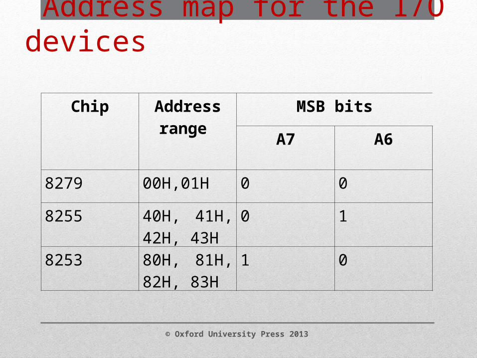
Address map for the I/O devices
Chip Address range
MSB bits
A7 A6
8279 00H,01H 0 0
8255 40H, 41H, 42H, 43H
0 1
8253 80H, 81H, 82H, 83H
1 0
© Oxford University Press 2013
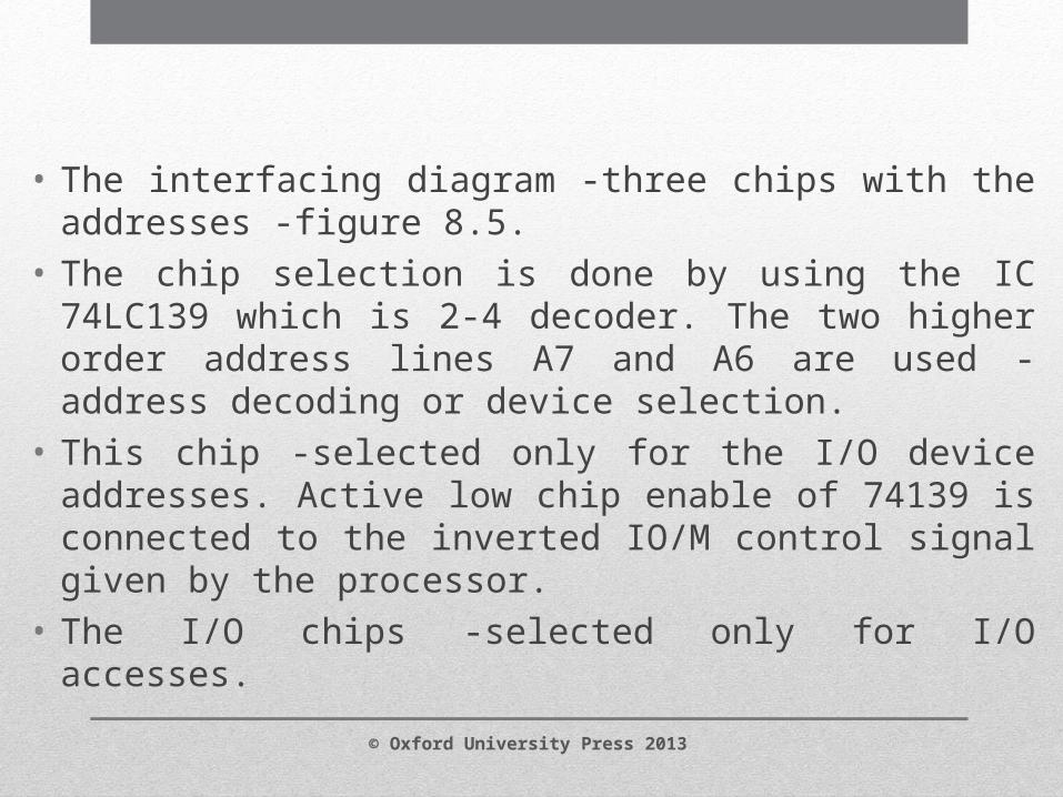
• The interfacing diagram -three chips with the addresses -figure 8.5. • The chip selection is done by using the IC 74LC139 which is 2-4
decoder. The two higher order address lines A7 and A6 are used -address decoding or device selection.
• This chip -selected only for the I/O device addresses. Active low chip enable of 74139 is connected to the inverted IO/M control signal given by the processor.
• The I/O chips -selected only for I/O accesses.
© Oxford University Press 2013
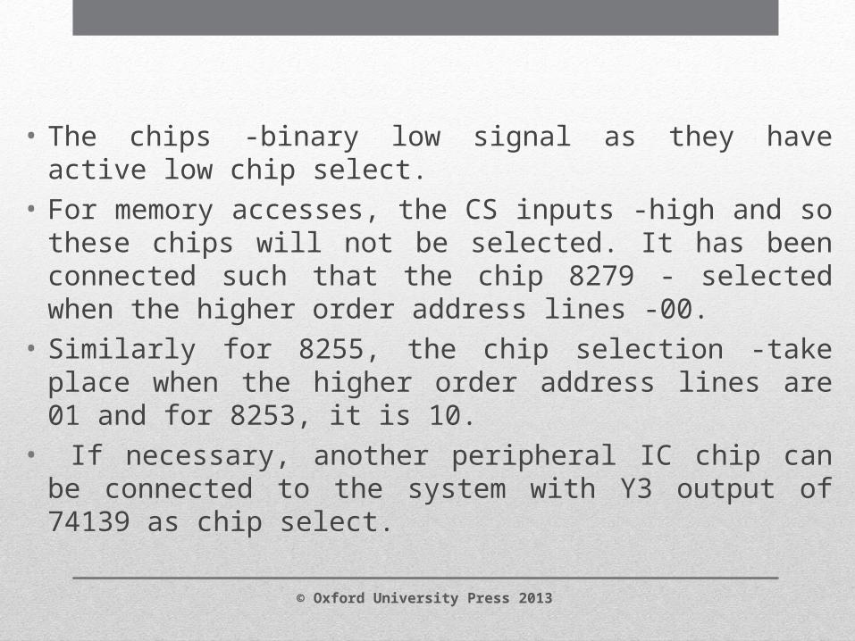
• The chips -binary low signal as they have active low chip select. • For memory accesses, the CS inputs -high and so these chips will
not be selected. It has been connected such that the chip 8279 - selected when the higher order address lines -00.
• Similarly for 8255, the chip selection -take place when the higher order address lines are 01 and for 8253, it is 10.
• If necessary, another peripheral IC chip can be connected to the system with Y3 output of 74139 as chip select.
© Oxford University Press 2013
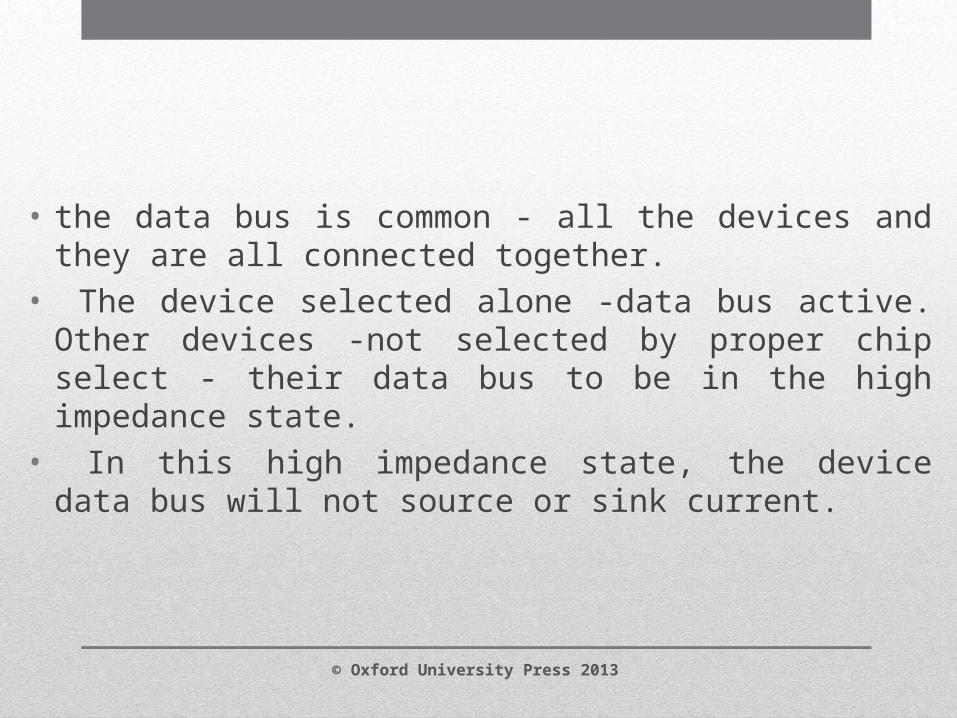
• the data bus is common - all the devices and they are all connected together.
• The device selected alone -data bus active. Other devices -not selected by proper chip select - their data bus to be in the high impedance state.
• In this high impedance state, the device data bus will not source or sink current.
© Oxford University Press 2013
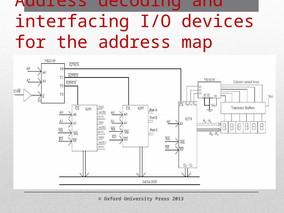
Address decoding and interfacing I/O devices for the address map
© Oxford University Press 2013
• To this -additional devices -ADC, DAC, LEDs, switches and LCD displays -connected
• Also more number of memory chips can be interfaced -adjusting the address map
© Oxford University Press 2013
• Intel supplies -additional support slave ICs -• These slave ICs - improve the functionality of the microprocessor
system and programming requirements. • These devices are popular -used not only with 8085, but with lot of
other microprocessors. Intel’s 16-bit processors - support interfacing these devices.
• The table 8.3 gives -basic functions of these support chips. operation, interfacing and programming can be obtained -datasheet of these chips.
Other supporting devices
© Oxford University Press 2013
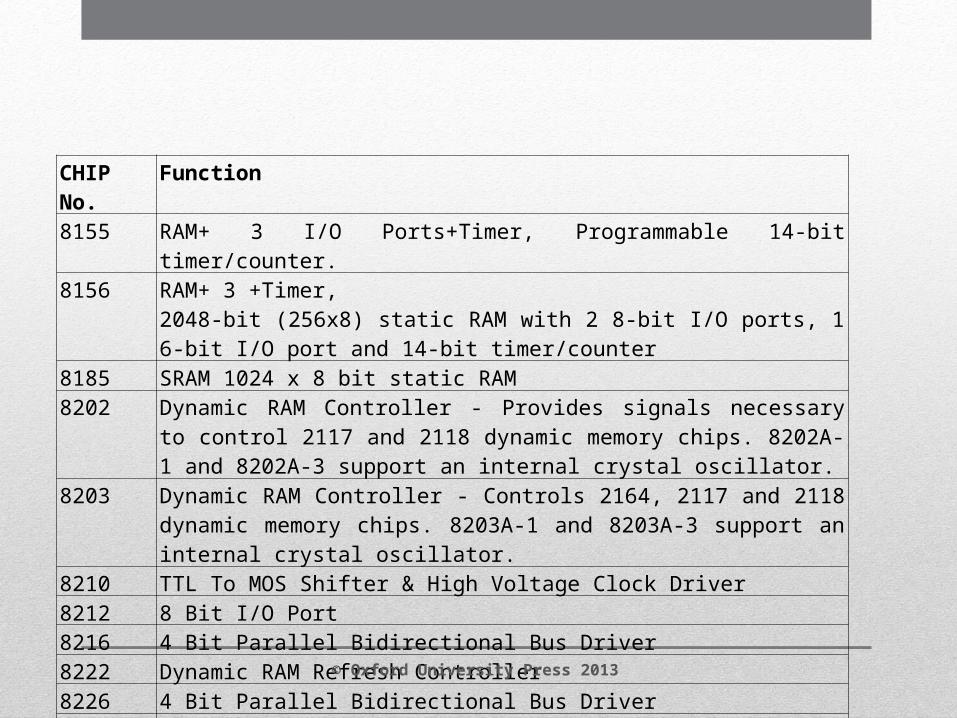
Intel’s Supporting Devices
CHIP No. Function
8155 RAM+ 3 I/O Ports+Timer, Programmable 14-bit timer/counter.8156 RAM+ 3 +Timer,
2048-bit (256x8) static RAM with 2 8-bit I/O ports, 1 6-bit I/O port and 14-bit timer/counter
8185 SRAM 1024 x 8 bit static RAM8202 Dynamic RAM Controller - Provides signals necessary to control 2117 and
2118 dynamic memory chips. 8202A-1 and 8202A-3 support an internal crystal oscillator.
8203 Dynamic RAM Controller - Controls 2164, 2117 and 2118 dynamic memory chips. 8203A-1 and 8203A-3 support an internal crystal oscillator.
8210 TTL To MOS Shifter & High Voltage Clock Driver
8212 8 Bit I/O Port8216 4 Bit Parallel Bidirectional Bus Driver8222 Dynamic RAM Refresh Controller
8226 4 Bit Parallel Bidirectional Bus Driver8231 Arithmetic Processing Unit
© Oxford University Press 2013
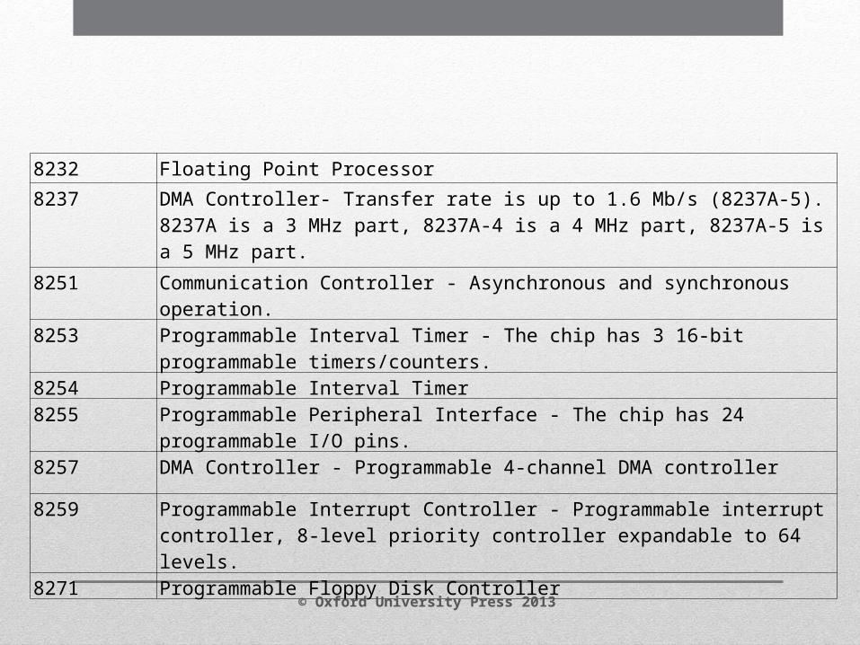
8232 Floating Point Processor
8237 DMA Controller- Transfer rate is up to 1.6 Mb/s (8237A-5).8237A is a 3 MHz part, 8237A-4 is a 4 MHz part, 8237A-5 is a 5 MHz part.
8251 Communication Controller - Asynchronous and synchronous operation.
8253 Programmable Interval Timer - The chip has 3 16-bit programmable timers/counters.
8254 Programmable Interval Timer
8255 Programmable Peripheral Interface - The chip has 24 programmable I/O pins.
8257 DMA Controller - Programmable 4-channel DMA controller
8259 Programmable Interrupt Controller - Programmable interrupt controller, 8-level priority controller expandable to 64 levels.
8271 Programmable Floppy Disk Controller
© Oxford University Press 2013
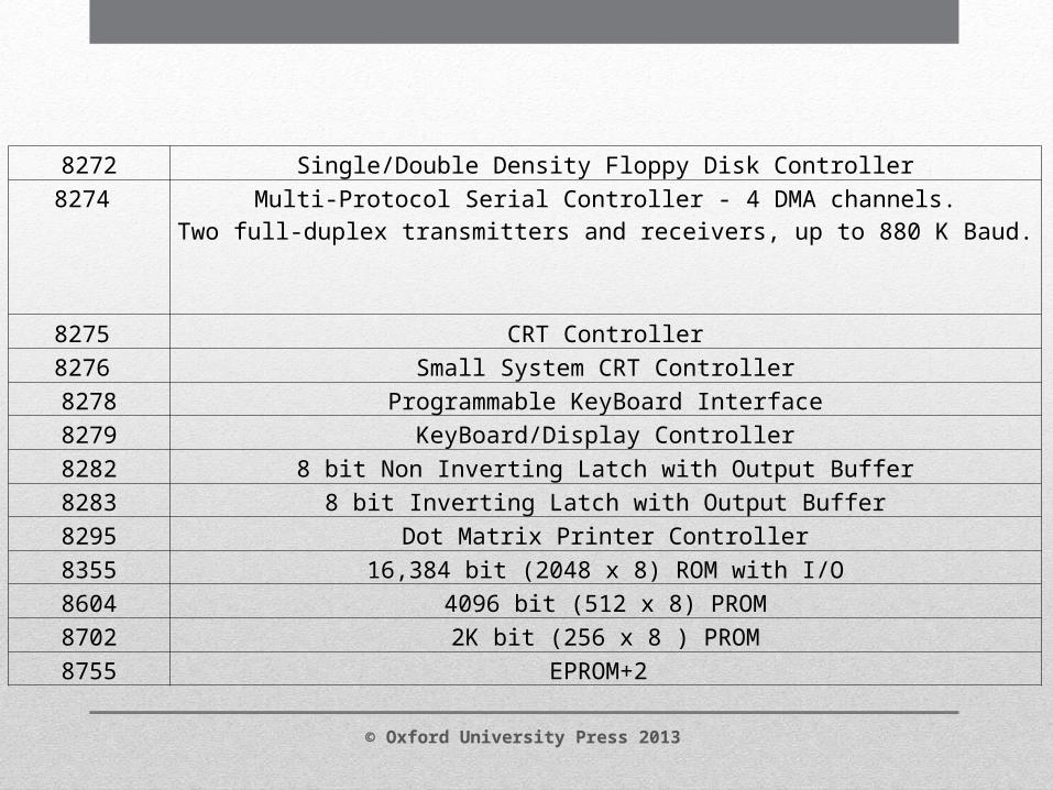
8272 Single/Double Density Floppy Disk Controller
8274 Multi-Protocol Serial Controller - 4 DMA channels.Two full-duplex transmitters and receivers, up to 880 K Baud.
8275 CRT Controller
8276 Small System CRT Controller
8278 Programmable KeyBoard Interface
8279 KeyBoard/Display Controller
8282 8 bit Non Inverting Latch with Output Buffer
8283 8 bit Inverting Latch with Output Buffer
8295 Dot Matrix Printer Controller
8355 16,384 bit (2048 x 8) ROM with I/O
8604 4096 bit (512 x 8) PROM
8702 2K bit (256 x 8 ) PROM
8755 EPROM+2
© Oxford University Press 2013
• The 8085 processor - at least one ROM and one RAM chip -complete microcomputer system.
• The system -at least one input device and one output device.• The address map -memory used and the I/O devices used must be
finalized before designing the address decoder.• The decoder chips such as 74138, 74139 can be used for address
decoding - microcomputer system. • The decoder -consider whether the chip select signals are active
low or active high.• The data bus is common and connected to all the devices in the
system.
Summary
© Oxford University Press 2013